U PD72120 Users Manual Dec86
uPD72120_Users_Manual_Dec86 uPD72120_Users_Manual_Dec86
User Manual: manual pdf -FilePursuit
Open the PDF directly: View PDF ![]() .
.
Page Count: 118 [warning: Documents this large are best viewed by clicking the View PDF Link!]
" "
NEe
Electronics
Inc.
NEe
ADVANCE
PRODUCT
INFORMATION
December
1886
pPD72120
Advanced Graphics Display Controller
User's Manual
The information contained in this
document
is being iIIued
in
adYance
of
the
produCtiOn cycle
for
the
device. The
parameters
for
the
device may change before final production
or
NEe
Electronics Inc
.•
~
It
its
own
discretion.
may
withdraw the ctevice prior
to
production.
The information in this document is subject
to
change without
notice.
NEe
Electronics Inc. assumes
no
responsibility
for
any errors
or
omissions that may appear
in
this document. Devices sold
by
NEe
ElectroniCS Inc.
are covered
by
the warranty and patent indemnification provisions appearing in
NEe
illectronics
Inc~
Terms and
Conditions of Sale only.
NEe
Electronics Inc. makes
no
warranty. express, ltatutory, implied,
or
by
desCription.
regarding the information
.t
forth herein
or
regarding
the
freedom
of
the
deSCribed devices from patent
infringement. NEC Electronics Inc. makes
no
warranty
of
merchantability
or
fitness
for
any purpose.
NEe
Electronics Inc. makes
no
commitment
to
update
or
to
keep current
the
information contained in this document.
No
pert
of
this document may
be
copied
or
reproduced in any form
or
by
any means
without
the
prior written
~nsent
of
NEC Electronics Inc.

..
Advanced
Graphic Display Controller
Preliminary Product Informat:ion
1.
OVerview
•••••••••••••••••••••••••••••••••••••••••••••••••••••••••
Features
•••••••••••••••••••••••••••••••••••••••••••••••••••••••
Pin
Configurations
•••••••••••••••••••••••••••••••••••••••••••••
Pin Configuration
(Flat
package)
••••••••••••••••••••••••••
Pin Configuration
(PLCC
package)
••••••••••••••••••••••••••
Block
Diagram
••••••••••••••••••••••••••••••••••••••••••••••••••
Pin
Functions
••••••••••••••••••••••••••••••••••••••••••••••••••
Clock Pins
••••••••••••••••••••••••••••••••••••••••••••••••
system
Bus
Control Pins
•••••••••••••••••••••••••••••••••••
Dis~ay
Memo~
Control Pins
•••••••••••••••••••••••••••••••
Video
Timing
Signal Helated Pins
••••••••••••••••••••••••••
Display Signal Belated Pins
•••••••••••••••••••••••••••••••
Power
SUpply
and
Ground
Pins
••••••••••••••••••••••••••••••
SmlTery
••••••••••••••••••••••••••••••••••••••••••••••••••••••••
2.
Function Description
•••••••••••••••••••••••••••••••••••••••••••••
2.1
Features
••••••••••••••••••••••••••••••••••••••••••••••••••••••••
High
Speed
Graphics
Drawing
••••••••••••••••••••••••••••••••••••
Video
Timing
Signal Generation
•••••••••••••••••••••••••••••••••
Large capacity Display
Memo~
COntrol
••••••••••••••••••••••••••
CPtJ
Interface
••••••••••••••••••••••••••••••••••••••••••••••••••
2 .2 Corrmand/Paranete r
Exchange
Between
the
CPU
and A(;x'
••••••••••••
2.3 Beset and Abort Operation
••••••••••••••••••••••••••••••••••••••
3.
A~
C>}?eration
•••••••••••••••••••••••••••••••••••••••••••••••••••
3.1
How
to
Use
the
Internal
~ister
••••••••••••••••••••••••••••••••
3.2
AGDC
Control
~isters
••••••••••••••••••••••••••••••••••••••••••
S'm'ltlS (
Status)
••••••••••••••••••••••••••••••••••••••••••••••••
BANK
(Bank)
••••••••••••••••••••••••••••••••••••••••••••••••••••
C'l'RI., (Control)
•••••••••••••••••••••••••••••••••••••••••••••••••
3.3 Display
~lated
~isters
•••••••••••••••••••••••••••••••••••••••
DI~Y
FLAGS
(Display Flags)
••••••••••••••••••••••••••••••••••
DISPLAT
PITCH
(Display Pitch)
••••••••••••••••••••••••••••••••••
AC
(Address Control)
•••••••••••••••••••••••••••••••••••••••••••
DAD
(Display Address)
••••••••••••••••••••••••••••••••••••••••••
~
(~rd
Count)
••••••••••••••••••••••••••••••••••••••••••••••••
GCSRX
(Graphics Cursor X Coordinate)
•••••••••••••••••••••••••••
CRS
(OJrsor
()Ut
Select)
••••••••••••••••••••••••••••••••••••••••
i
1-1
1-1
1-2
1-3
1-4
1-5
1~
l~
1-6
1-8
1-9
1-9
1-9
1-10
2-1
2-1
2-1
2-3
2-3
2-3
2-5
2-9
3-1
3-1
3-3
3-3
3-5
3~
3-7
3-6
3-14
3-15
3-16
3-17
3-18
3-19
Advanced
Graphic Display
Controller
CE
(CUrsor
D~lay
Enable)
•••••••••••••••••••••••••••••••••••••
OCSRYS
(Graphics Cursor Y COOrdinate
Start)
••••••••••••••••••••
G:RSl'E (Graphics CUrsor Y OX>rdinate
End)
••••••••••••••••••••••
BS,
BBP,
BH, BO,
BFP
•••••••••••••••••••••••••••••••••••••••••••
VS,
VBP,
LlF,
VFP
••••••••••••••••••••••••••••••••••••••••••••••
3.4
Inter.nal
Register
~le
•••••••••••••••••••••••••••••••••••••••••
3-20
3-21
3-22
3-23
3-24
3-25
4.
Drawing
Operations
•••••••••••••••••••••••••••••••••••••••••••••••
4-1
4.1
Drawing
Functions
•••••••••••••••••••••••••••••••••••••••••••••••
4-1
4.2
~
of
DRAW
Commands
••••••••••••••••••••••••••••••••••••••••••
SUmma~
of
Operation Flags
•••••••••••••••••••••••••••••••••••••
4.3
Detailed
Description
of
DRAW
Commands
•••••••••••••••••••••••••••
4.3.1
Register Operation
COmmands
•••••••••••••••••••••••••••••
4.3.2
Graphics
Drawing
Commands
•••••••••••••••••••••••••••••••
4.3.3
Paint
Commands
••••••••••••••••••••••••••••••••••••••••••
4.3.4
CDPY
Commands
•••••••••••••••••••••••••••••••••••••••••••
4.3.
5
PUT/~T
COrmands
4.4
How
to
Use
the
Flag
Bits
••••••••••••••••••••••••••••••••••••••••
••••••••••••••••••••••••••••••••••••••••
4.5
Painting
Pattern
~ferenoe
Examples
•••••••••••••••••••••••••••••
4.6
Inter-plane
Data Transfers
••••••••••••••••••••••••••••••••••••••
4.7 Drawing
~lated
~isters
•••••••••••••••••••••••••••••••••••••••
4.8 Parameters Corresponding
to
DFAW
Commands
•••••••••••••••••••••••
ii
4-1
4-4
4-9
4-9
4-10
4-20
4-25
4-30
4-32
4-43
4-46
4-47
4-55
Advanced
Graphic
Display
COntrolle
r
Section
1
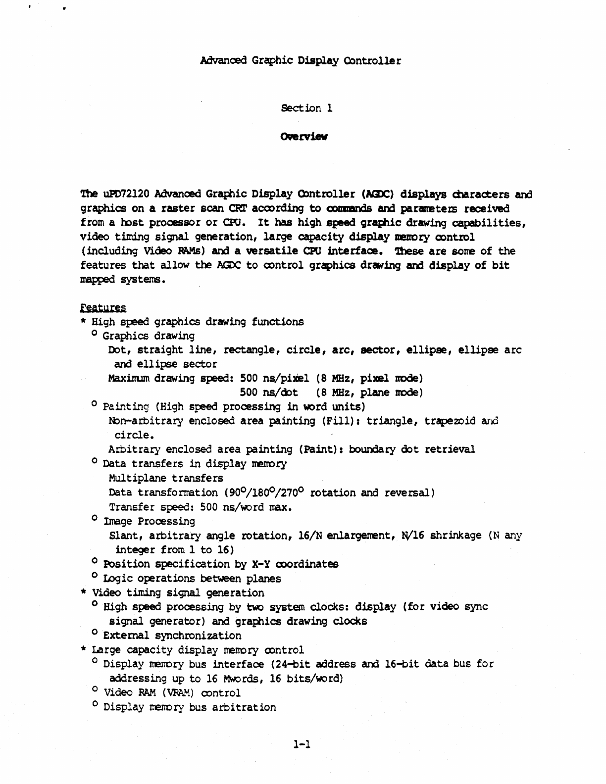
'n1e
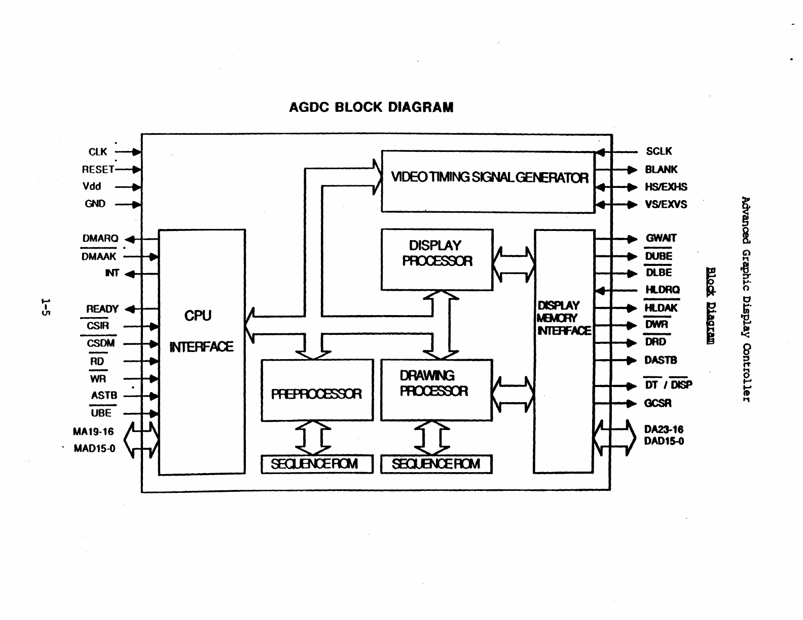
uP072120 Advanced
Gratilic
Display
Olntroller
(HDC)
displays
characters
and
graphics
on
a
raster
scan
CRr
aC(X)rding
to
coummds and pararretez:s received
from a h:>st processor
or
CPO.
It
has
high
speed
graPlic
drawing
capabilities,
video
timing
signal
generation,
large
capacity
display
IDeDDtY
ex>ntml
(including
Video
RAMs)
and a
versatile
CPO
interface.
'!hese
are
sene
of
the
features
that
allow
the
ACZX:,
to
ex>ntrol
graphics
dr_ing
and
display
of
bit
~
systems.
Features
* High
speed
graphics
drawing
functions
o
Graphics
drawing
!:bt,
straight
line,
rectangle,
circle,
are,
sector,
ellipse,
ellipse
arc
and
ellipse
sector
Maxirrum
drawing speed:
500
ns/piXel
(8
MHz,
pixel
node)
500
ns/d:>t
(8
MHz,
plane DDde)
o
Painting
(High speed
processing
in
word
units)
N:>n-arbitrary
enclosed
area
painting
(Fill):
triangle,
trapezoid
and
circle.
Arbitrary
enclosed
area
painting
(Paint):
boundary
&:>t
retrieval
o
Data
transfers
in
display
menory
Multiplane
transfers
Data
transfomation
(90°/180°/270°
rotation
and
reversal)
Transfer
speed:
500
ns/word
max.
° Image
Processing
Slant,
arbitrary
angle
rotation,
16/N
enlargenent,
W16
shrinkage
(N
any
integer
from 1
to
16)
o
Position
specification
by
X-Y
coordinates
o
IDgic
operations
between
planes
*
Video
timing
signal
generation
o High
speed
processing by two system
clocks:
display
(fo
r
video
sync
signal
generator)
and
gratilics
drawing
clocks
o
External
synchronization
* Large capacity
display
memo~
control
o
Display
menory bus
interface
(24-bit
address
and
16-bit
data
bus
fo
r
addressing
up
to
16
Mwords,
16
bits/word)
° Video
RAM
(VPAM)
oontrol
o
Display
memory
bus
arbitration
1-1
Advanced
Gr~hic
Display
Controller
*
IiJst
Processor
(CPU)
Interface
o System
bus
interface
-
-2o-bit
address
bus,
8
or
16
bit
data
bus
o
SYStem
ueItOry <->
display
nenory
data
transfer
with
extemal
IJ.1A
Controller
From
system
merrory
to
display
DeltCry (PU!')
From
display
uencry
to
system
meItDry
tCET)
o
Sigh
speed
pipeline
processing
with
preprocessor
before
drawing
processor
o
CPO
DerlDry
or
I/O
mapping
of
internal
registers
and
display
menory -
efficient
~stem
interface
* 8
MHz
System
Clock
*
CHJS
Technoloqy
*
Single
+5
V
Power
SJpply
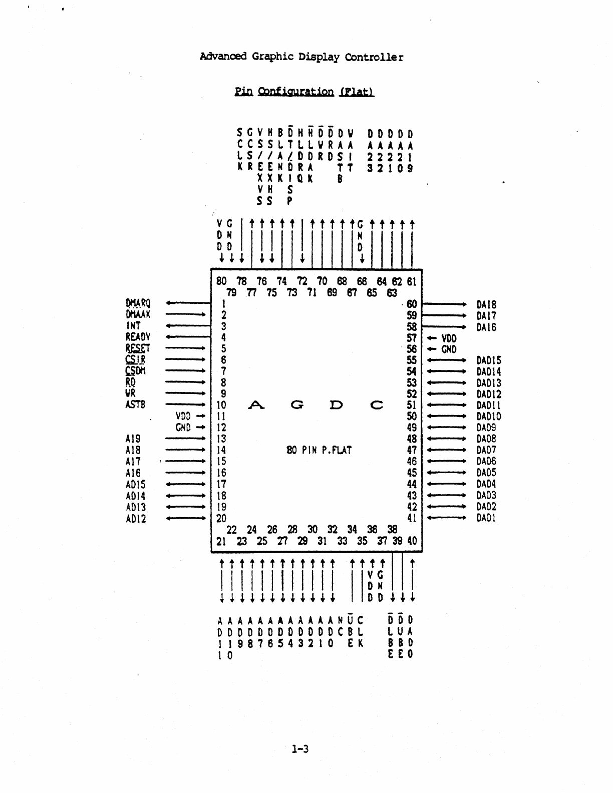
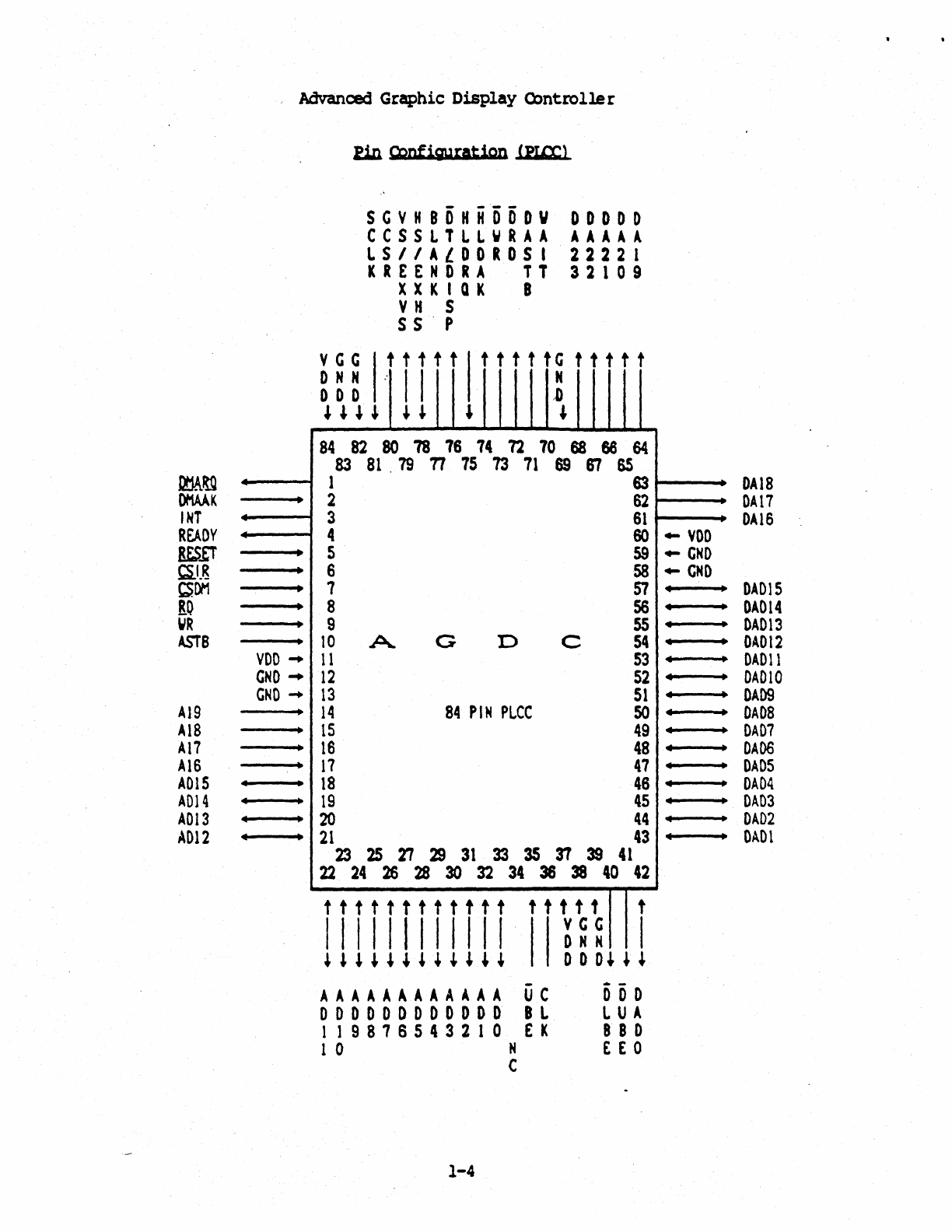
* SO-pin
flat
package (uPD72l2DG)
or
84-pin
PICe
(uPD72l2OL)
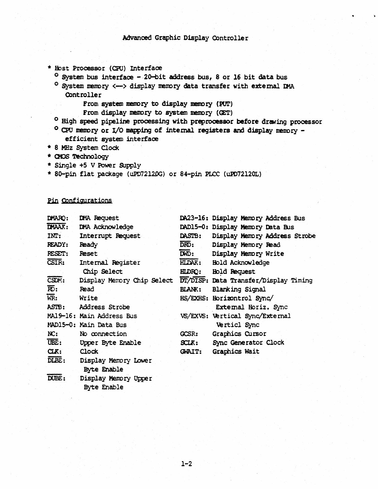
Ein
Configurations
~:
II1A
lequest
IJt\AAK:
II-1A
Acknowledge
INT:
Interrupt
~est
R'.ADY:
leady
RESET:
~set
CSIR:
Internal
~ister
Chip
Select
CS5M:
Display
Menory
Chip
select
R):
Read
WR:
Write
ASl'B: Address Strobe
MAl9-l6:
Main Address
Bus
l-1AD1S-o:
flain
Data
Bus
NC:
R:>
ex>nnection
USE:
Oppe r
Byte
Enable
CI.K:
Clock
DfBE:
-
DUBE:
Display
Memory
Lower
Byte
Enable
Display
Memory
Upper
Byte
Enable
W3-l6:
Display
Ment>ry
Address. Bus
IW>l5-o:
Display
Mem:>ry
Data
Bls
D.l\Sm:
Display
Memory
Address Strobe
~:
Display
MeIIOry
lead
'00:
Display
MenDry
Write
~:
9;)ld
Acknowle:lge
BLD~:
9;)ld
~est
DT/I5ISP:
D:lta
Transfer/Display
Timing
~:
Blanking
Signal
HS/EXHS:
9;)ri2Dntrol
Sync!
.
Exte
mal
Ii:>
r
iz.
Sync
VS/EXVS:
~rtical
Sync/External
va
rticl
Sync
GCSR:
Gratilics
CUrsor
s:LK: Sync Generator
Clock
~T:
Graphics
wait
1-2
~~
Ot1AAK
INT
READV
Jt£S£T
CSJ]
C.SDM
RO
WR
ASTB
A19
Al8
At7
Ale
AOtS
•
AOl4
..
ADt3
•
A012
•
Advanced Graphic
Display
Controlle
r
~
•
•
~
•
..
•
VOO
....
GND
....
..
•
•
•
II
•
II
II
E1D.
Cbnfiguration
(Plat)
SCVHBDHHODOV
CCSSl.TLLWRAA
LSIIAI.DORDS
I
K R £ £
NOR
A T T
XXKICk
B
V H S
SSP
00000
A A A A A
22221
3 2 1 0 9
vc
ttttt
tttftcttttt
~
~
II
~
~
~
~
,~~
~
80
78
76
74
72
70
88
68 64
82
61
79
T1
75
73
71
69 67
as
63
1 -60
2
59
3
58
4
51
5
56
6
55
7
54
8
53
9
52
10
A.
G D C
51
11
50
12
49
13
48
14
80
PIN
P.f'l.AT
47
15
46
16
45
17
44
18
43
19
42
20
41
22
24
26
28
30 32
34
38
38
21
23
25 27
29
31
33
35
37
39
40
, t t t t , t t t t t t t t t t t
I I I I I I I I I I I I
VG
I
o N
+ + + + + + + +
~
+
~
~
o 0
~ ~
+
A A A A A A A A A A A A N U C D D 0
o 0 0 0
DOD
0
DOD
0 C 8 L L U A
1 1
987
654
3 2 1 0 £ K B B 0
1 0 E E 0
1-3
OAI8
OAl7
DAI6
..
VOD
..
eND
•
~
DADtS
• Ii
OAD14
4
~
DADI3
• Ii
DAD12
• Ii
DADlt
4
Ii
DADlO
•
II
OAD9
•
II
DADa
•
II
DAD7
• •
DADS
• •
DADS
• •
OAD4
•
II
DAD3
• •
OA02
• •
DADl
fljAtQ
DMAAK
tNT
READY
&ES.ET
CSJ.&
CS~
&0
WR
AST8
A19
AlB
A17
AIS
AOlS
A014
AOl3
AD12
Advanced
Graphic
Display
Q)ntrolle
r
tin
Q:mfiguration
(PTa'l
sevHsDHiiooov
00000
CCSSLTLLWRAA
AAA.AA.
LSI
I
A.
l 0 0 R 0 S I
222
2 1
K R E £ N D
RAT
T
321
0 9
XXKIQK
B
V H S
ss·p
vee
ttttt
tttttcttttt
~~~
:
II
~
~
~ ~ ~ ~
~,
,
84
82 80
18
76
74 72
70
68
66 64
83
81
79
77
75 73
71
69 67
6S
1
631---
..
----..
2
62
1-----.
3
61~--"
4
~
~voo
----..
5
59
~
eND
----..
6
58
~
eND
----..
7
57
..
•
----..
8
~
~.--~
•
-----..
9 M
~
..
--~
•
----..
10
A.
G D C
54
~.-~
•
VDD
-.
11
53
+-.-~
•
eND
-.
12
52
+-.-~
•
•
eND....
13
51
~
..
-~
•
14
84
PIN
PLCC
50
~
..
-~
•
----..
15
49
~
..
-~
•
----..
16
48
....
-
....
•
----+.
11
47
~.-~
•
• •
18
46
~.-
....
•
• •
19
45
....
-~
I
•
..
•
20
44
..
4-
....
•
..
•
21
43
"'4-~
23
2S
2'7
29
31
33
35
37
39
41
22
24
26 28
30
32
34
36 38
40 42
t t t t t t t t t t t t t t t t f t
II
t
II1III111
~
~
~
I
~~~~,+".~,.
DOD'~~
AAAAA.AA.AAAAA
UC
DOD
o
DOD
0
DOD
0
DOD
B L L U A
1 1
987
654
321
0 £ k B B 0
ION
£ E 0
C
1-4
OAI8
DA17
DAIS
OADIS
DAD14
OAD13
OAD12
DAD1!
DADI0
OAD9
DADS
DAD?
DADS
DADS
DAD4
DAD3
DAD2
DADI
f-t
eLK
RESET
Vdd
GND
OMARa
OMAAK
NT
J,
READ'
CSIR
CSOM
RD
WR
ASTI
UBE
MA19-1
.
MAD15
CPU
INTERFACE
AGDC BLOCK DIAGRAM
VIDEO
TIMING
SGW.GBERA~
DISPLAY
~
DISPlAY
t.IMRf
NTEFFACE
00AVVN2
~
~
SClK
BLANK
HSIEXHS
VSlEXVS
I
GWNT
~
DUDE
G)
t1
DlBE
E t
....
HlDRQ
0
I c
HLDAK
In·
-
~
own
~
DAD
g
DASTB
~
--
a
OT
I
DISP
....
to
GCSR
..,
0m.18
DAD15-0
Advanced
Gr~hic
DisplayOont~ller
i.in
Functions
Clock
Pins
I TeDninal I
I/O
I
Active
I
Name
I I
level
I
I
System
Bus
Cbntrol
Pins
I Terminal
I
Narre
I/O
I
Active
I
level
I MADlS-o I
I/O
I
I I I
I MAl9-16 I
I·
I
Function
I Clock
sut¢ied
to
the
circuits
other
than
the
I
the
sync
signal
generator
and
display
processor.
I
'1'he
drawing
processor
am
preprocessor
speed
I depend on
this
clock
frequency.
I Clock
supplied
to
the
sync
signal
generator
and I
I
the
display
processor.
'.this
clock
frequency
is
I
I
determined
by
the
eRr
timing
requirenents
-
i.e.,
I
I
b:>rizontal
sync
frequency,
the
nUll'ber
of
dots
per
I .
I
line,
etc.
I
Function
I/O
bus
to
the
cro
ex>nsisting
of
nultiplexed
16-
I
bit
address
and a
bidirectional
data
bus.
I upper
four
address
bits
of
the
20-bit
address.
+
ASTB
I I
I
E I
Latches
the
address
on
MAl9-16
and
l-1AD1S-O
on
the
I
falling
edge.
USE
I I
I
I
I
I
I
I
I
L I
'lbgether
with
JW)()
defines.
the
data
acoess
fotltBt
I
as
shown
below.
tlBE
smuld
be
tied
high
when
I oonnected
to
an
8-bit
CPO.
I
~
tlBE
Di.tA
ACa!ss
Fonna
t
I 0 0 Even
address
word
I 0 1 Even
address
byte
I 1 0
~d
address
byte
I 1 1
Odd
address
byte
1-6
Advanced
Graphic
Display
Controller
System Bus
Control
pins
(oontinued)
'n!rmina.l I I/O I
Active
Function
Name
I I
level
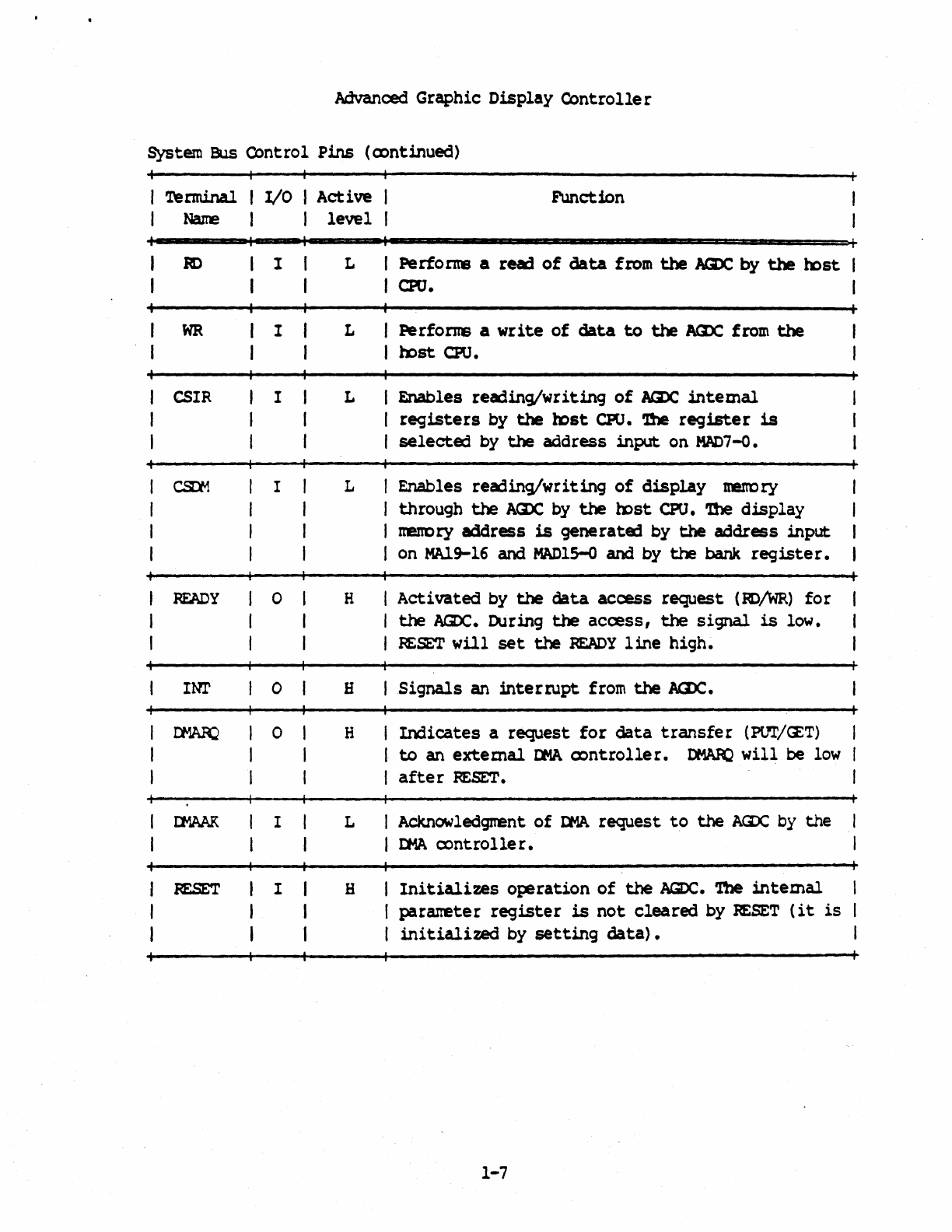
RD
I L I
PerfOnt8
a read
of
data
from
the
NZY:, by
the
~st
I
CPO.
WR
I L
Perforns
a
write
of
data
to
the
ACDC
from
the
mst
CPU.
CSIR I L I Enables
reading/writing
of
laX:.
intemal
I
registers
by
the
mst
CPO.
'Dle
register
is
I
selected
by
the
address
input
on
MNl7-o.
CSl1
I L I Enables
reading/writing
of
display
uenory
I
through
the
Ar:D:
by·
the
mst
CPU.
'l'he
display
I rrerrcry
address
is
generated
by
the
address
input
I on
MAl9-16
and
MADl5-0
and by
the
bank
register.
RFADY
0 H I
Activated
by
the
data
access
request
(R>/WR)
for
I
the
AaX:.. During
the
access,
the
signal.
is
low.
I
~$T
will
set
the
READY
line
high.
IN!' 0 H
Signals
an
interrupt
from
the
AaX:..
~
0 H
Indicates
a
request
for
data
transfer
(PUT/GET)
to
an
extemal
~
ex>ntroller.
DMARO
will
be
low
afte
r
RESET.
Il1AAK
I L I Acknowledgnent
of
tt-1A
request
to
the
AGX
by
the
I
DMA
controller.
!£SET I H I
Initializes
operation
of
the
AGOC..
The
intemal
I
paraneter
register
is
not
cleared
by
H:SET
(it
is
I
initialized
by
setting
data).
1-7
Advanced
Graphic
Display
Controller
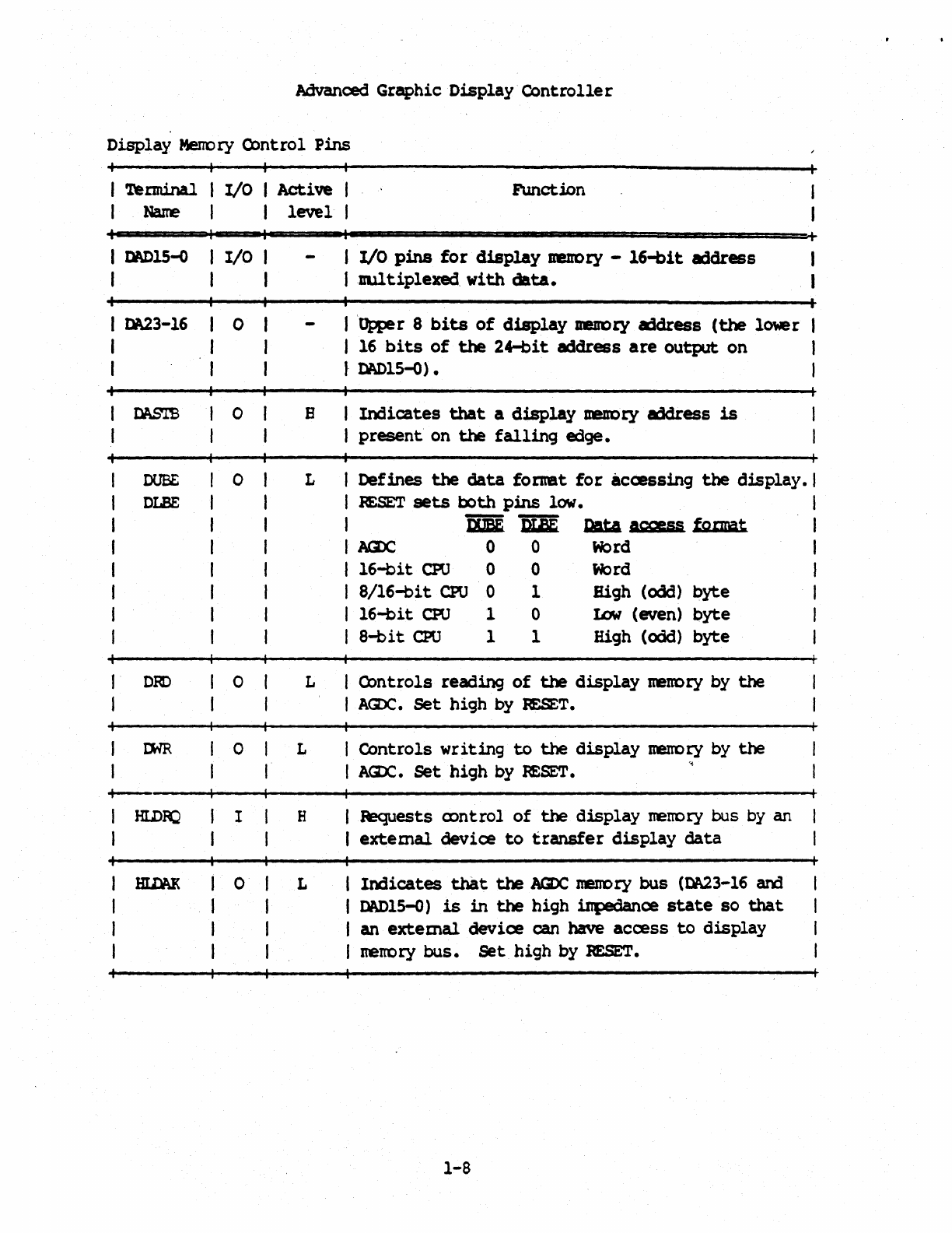
Display
MeIrory
O:>ntrol
Pins
I
'1eminal
I
I/O
I
Active
I
I
Name
I I
level
I
Function
I
J:W)lS~
I
I/O
I
I I I
I
DA23-16
I
I
DUBE
DLBE
DR)
o
o
0
o
o
I
I/O
pins
for
display
DeDDty -
16-bit
mdress
luultiplexed.
with
data.
I 'Opper 8
bits
of
display
DeDOty
Iddress
(the
lower
I 16
bits
of
the
24-bit
address
are
output
on
I
IW>lS-o).
B I
Indicates
that
a
display
DeltDty
address
is
I
present
on
the
falling
edge.
L I Defines
the
data
fornat
for
accessing
the
display.
I
I
:RESET
sets
Ix>th
pins
low.
I
iiii
iim
JatI.
eme
ss
fQgnat
I /IGX:, 0 0
Word
I
16-bit
CPO
0 0
Word
I
8/16-bit
CPU
0 1 High
(odd)
byte
I
16-bit
CPO
1 0 Low
(even)
byte
I
8-bit
CPU
1 1 High
(odd)
byte
L I
O:>n
trols
reading
of
the
display
meoo
ry
by
the
I
AG:X:,.
Set
high
by
m:sET.
L I
Controls
writing
to
the
display
nenory
by
the
"
I AGX,.
Set
high
by
RESET.
+-------~---+------~------------------------------------~
HIDKJ
I H
o L
I
aequests
control
of
the
display
menory bus by an
I
extemal
device
to
transfer
display
data
I
Indicates
that
the
NZX:,
mem:>ry
bus
(W3-16
arx1
I [w)15-0)
is
in
the
high
iJrpedanoe
state
so
that
I an
extemal
device
can have
access
to
display
I nenory
bus.
Set
high
by
RESET.
1-8
Advanced Graphic
Display
Centrolle
r
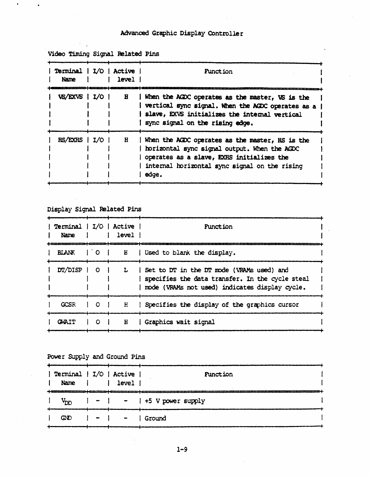
Video Timing Signal.
~latec1
Pins
I 'l'enninal I
I/o
I Active I
I
Name
I f
level
I
Function
vs/EXVS
I I/O I
I I
I I
I I
HS/EXHS
I
I/O
I
I I
I I
I I
I I
B I
When
the
laX;
operates
as
the
master,
VS
is
the
I
vertical
sync
signal.
When
the
NZJC
oparates
as
a
I
slave,
EXVS
initializes
the
intemal
vertical
I sync signal. on
the
rising
edge.
H I
When
the
AaX;
oparatee
as
the
master,
as
is
the
I
mrizontal
sync
signal
output.
When
the
AGDC
I
operates
as
a
slave,
EXHS
initialias
the
I
intemal
mrimntal
sync
signal
on
the
rising
I edge.
Display
Signal
Related
Pins
I 'l'e
rminal
I
I/O
I
Active
I
Name
I I
level
Function
+,======~~==*======+=====-==========-======================+
B.I.Mi(
I'
0
M/DISP I 0
I
I
GCSR
0
GlAIT 0
H
Used
to
blank
the
display.
L
Set
to
M
in
the
DT
nDde
(VPAMs
used)
aM
specifies
the
data
transfer.
In
the
cycle
steal
I
ItDde
(VPAMs
not
used)
indicates
display
Cjcle.
E I
Specifies
the
display
of
the
graphics
cursor
H I
Graphics
wait
signal
Power SUpply and Ground
Pins
J
Terminal
I
I/O
I
Active
I
Name
I I
level
+
I -
I -
Function
I
+5
V
powe
r
supply
I Ground
1-9
Advanced.
Graphic
Display
Controlle
r
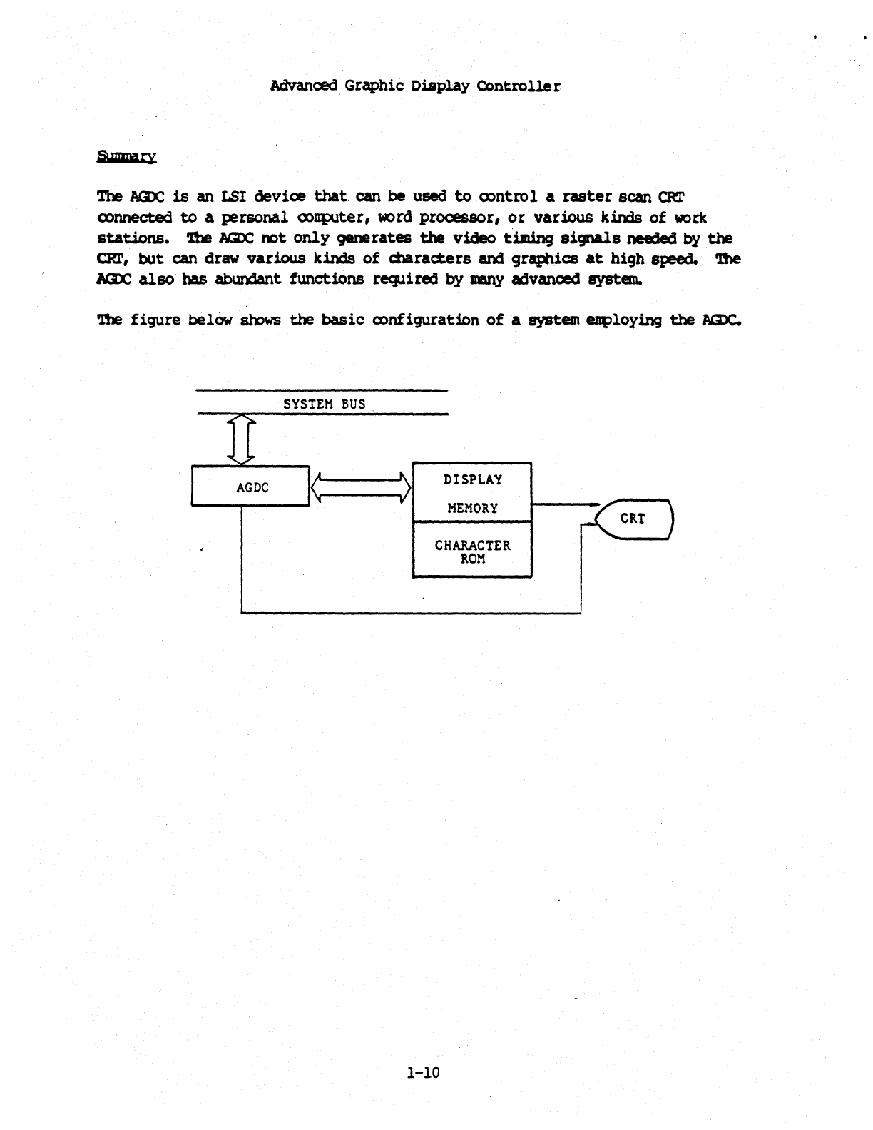
The
AGX.
is
an LSI device
that
can
be
used
to
(X)ntro
1 a
raster
scan
CRT
(X)nnecteQ
to
a personal
(X)lIp-lter,
word
processor,
or
various kinds
of
work
stations.
'1'be
AGOC,
not
only
generates
the
video t'iming
signals
needed
by
the
CRr,
but
can
draw
various kinds
of
maracters
and gratXUcs
at
high speed. '!be
lax:
also
bas
abundant
functions
required
by
many
advanced
system.
'!be
figure
below
sb:>ws
the
basic
ex>nfiguration
of
a system euploying
the
AGX.
SYSTEM
BUS
......
_..,..----'
<~>
DISPLAY
MEMORY
CHARACTER
ROM
1-10
Advanced Graphic Display
Centrolle
r
section
2
2.1
Features
High
Speed
Graphics Drawing
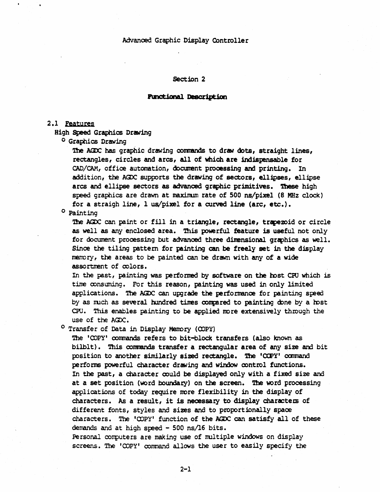
o Graphics Drawing
'!be
AaX
has
graphic
drawing
oormands
to
draw
oots,
straight
lines,
rectangles,
circles
and
arcs,
all
of
which
are
indispensable
for
CAD/CAM,
office
autonation,
cX>current
processing
am
printing.
In
addition,
the
At;zX;
supports
the
drawing
of
sectors,
ellipses,
ellipse
arcs
and
ellipse
sectors
as advanced
graphic
primitives.
'1hese
high
speed
graphics
are
drawn
at
maxirtum
rate
of
SOO
ns/pixel
(8
MHz
clock)
for
a
straigh
line,
1
us/pixel
for
a curved
line
(are,
etc.).
o
Painting
'!be
AaX,
can
paint
or
fill
in
a
triangle,
rectangle,
trapezoid
or
circle
as
well
as
any
enclosed
area.
'!his
powerful
feature
is
useful
not
only
for
docunent
processing
but
advanced
three
dinensional
graphics
as
well.
Since
the
tiling
pattern
for
painting
can
be
freely
set
in
the
display
merrory,
the
areas
to
be
painted
can
be
drawn
with
any
of
a wide
assortnent
of
oolors.
In
the
past,
painting
was
perfomed
by
software
on
the
mst
au
which
is
time oonsuming. For
this
reason,
painting
was
used
in
only
limited
applications.
The
AaX:,
can upgrade
the
performance
for
painting
sp?eO
by as nuch as
several
hundred
tines
oonpared
to
painting
c:bne
by a
mst
CPU.
This
enables
painting
to
be
applied
nore
extensively
through
the
use
of
the
AGDC.
o
Transfer
of
Data
in
Display
Merrory
(CDPY)
'!be
'cx)PY'
oorrmands
refers
to
bit-block
transfers
(also
known
as
bilblt).
'!his
CX)rmands
transfer
a
rectangular
area
of
any
size
arxl
bit
position
to
another
similarly
siEd
rectangle.
1be
'CCPY'
canmand
performs powerful
character
drawing and
window
oontrol
functions.
In
the
past,
a
character
oould be
displayed
only
with
a
fixed
size
and
at
a
set
p:>sition (word
boundaty)
on
the
screen.
1be
word
processing
applications
of
today
require
!rore
flexibility
in
the
display
of
characters.
As
a
result,
it
is
neoessaty
to
display
charactecs
of
different
fonts,
styles
and
sizes
and
to
proportionally
space
characters.
The
'CDPY'
function
of
the
AGX
can
satisfy
all
of
these
demands
and
at
high
s~ed
-500 ns/16
bits.
Personal computers
are
making use
of
multiple
windows
on
display
screens.
The
'ropy'
oorrrnand
allows
the
user
to
easily
specify
the
2-1
Advanced
Graphic
Display
Q:)ntrolle r
nUJtbe
r,
shape
and
size
of
IEUltiple
windows.
Purthe
r,
the
'Qpy'
oanmand
of
the
ND:
can perform
various
logical
operations
between source
an::1
destination
planes.
o
Image
Prooessing
'!be
NZ1:.
is
able
to
do
mre
than
just
copy
data.
It
can
slant
oopy,
arbitrary
angle
rotation
CDPY,
16/n
enlargeuent
cx>py
or
n/16
shrink
CX)py
(n
any'
integer
from 1
to
16).
ihese
copies
transfer
data
from a
rectangular
source
area
to
a non-rec::tangW.ar
destination.
n.
slant
Q)PY
can be used
for
drawing
italic
cbaractem.
'!be
atbitraty
angle
rotation
oopy
is
useful
for
doctment
preparation
beca1se
it
can
rotate
characters,
graphics,
imsges,
etc.
1be
enlarge and
shrink
oopies
are
effective
for
editing
and
patching
doclments.
'lbese
AGX:,
ootrltBOOs
relieve
the
mst
CPO
of
what
was
a
software
intensive
function.
'!be
laX:,
can
quickly
acoorrplish
these
image
processing
tasks
and
for
a lower
cost.
o
Position
Specification
by
X-Y
Q)ordinates
'nle
graphics
drawing and oopy
paranetem
can be
given
as
X-Y
ooordinates
thereby
relieving
the
mst
CPU
of
the
address
calculation
requirenents.
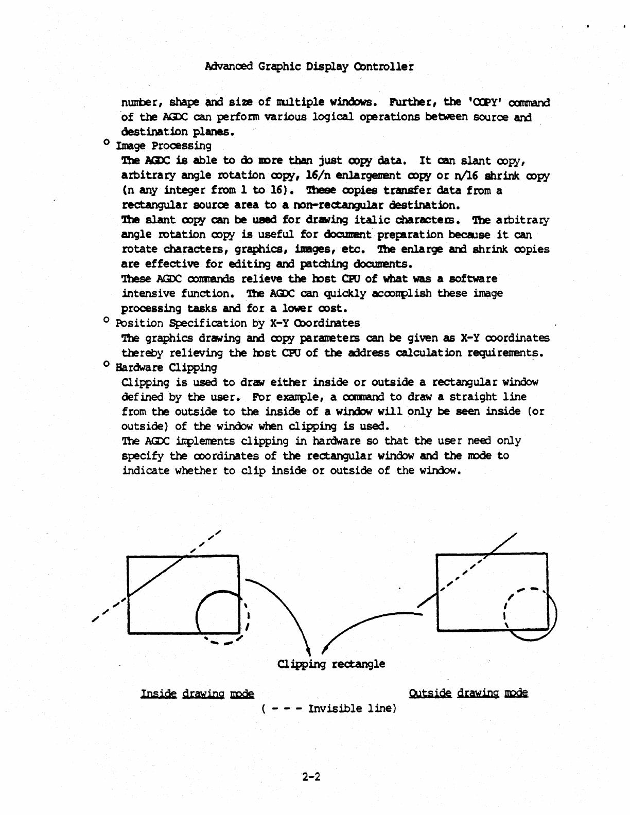
o Hardware
Clipping
Clipping
is
used
to
draw
either
inside
or
outside
a
rectangular
window
defined
by
the
user.
For
exanple,
a
cxm.nand
to
draw a
straight
line
from
the
outside
to
the
inside
of
a wirWw
wlllonly
be
seen
inside
(or
outside)
of
the
window
when
clipping
is
used.
'!be Aax:. inplements
clipping
in
hardware so
that
the
user
need only
specify
the
cx>ordinates
of
the
rectangular
winoow
and
the
mde
to
indicate
whether
to
clip
inside
or
outside
of
the
window.
Clipping
rectangle
Inside
drawing
~
( - - -
Invisible
line)
2-2
I
,
,
\
~
-,
OUtside
drawing
~
Advanced Graphic
Display
Controlle
r
Video Timing
Signal.
Generation
o High
Speed
Processing
by
Dual System
Clocks
Dual system
clocks
can
be
input
to
the
NZX':.
-
the
drawing
clock and
the
display
clock.
In
a
graphics
system,
the
display
rate
depends
on
the
resolution
of
the
CRr,
the
clock
frequency
of
the
display
mntrolle
r
depends on
the
display
rate.
In
the
past,
only
a
single
clock
was
used
for
the
display
a>ntroller.
It
was
often
necessary
to
limit
the
clock
to
5
MHz
even
trough
the
capacity
of
the
display
ex>ntrolle r
was
8
MHz.
'lberefore,
the
AaX:,
was
designed
to
have
the
display
clock
independent
of
the
drawing clock
so
that
drawing can
be
perforned
at
the
highest
tx>ssible
speed.
o
External
Sync
Inplt
In
systems
that
incx>rporate a
separate
circuit
to
generate
the
video
timing
signals
and use an
Aczx,
only
to
draw
gra];ilics,
or
in
systems
that
use
JIUltiple
AGDCs
to
achieve
higher
perfoanance,
it
is
necessar:y
to
synchronize
the
ACD:.
with
the
extemal
Circuitry
or
the
AiD:
with
other
AGDCs.
'1berefore,
the
1Q.X,
has
extemal
sync
input
capability
to
synchronize
its
operatlons
with
other
A£J)Cs
or
with
extemal
circuitry.
Large
capacity
Display
Menory
Control
o
~isplay
Mem:ay
Bus
Interface
With
its
24-bit
addressing
and
16-bit
data,
16
Mwords
of
16
bits/word
display
nerrory can
be
cx>nfigured
with
the
ACDC.
'!his
neans
that
up
to
64
planes
of
2048 x 2048
dots
can
be
cx>nnected.
o
Video
MM
(VRAM)
Q)ntrol
VPAMs
are
dual-p:>rted
DRAMs
with
intemal
line
buffer
shift
registers
(i.e.,
uPD41264). '!be
VMMs
provide
a
sep!lrate
port
for
display
data
so
that
when
drawing, JIel'Il)ry
access
tine
is
greatly
reduC2d. As a
result,
nost
of
the
entire
rreItDry
cycle
can
be
used
as
the
drawing
cycle
to
inprove system
throughput.
'nle
AGDC
supplies
the
signals
neEded
to
oontrol
VRAMs.
o
DisplayMemo~
Bus
Ar.bitration
In
a
basic
system,
the
display
ment>ry
is
accessed
by
the
AQ)C
only.
However,
in
a
nore
advanced system,
the
display
menory
may
be
accessed
by
other
processors.
In
other
words, a
local
bus
is
established
between
the
display
nen:cry and
the
Ja)C
or
other
processors.
In
this
case,
it
is
necessary
for
the
AaX:,
to
periodically
provide
refresh
am
display
cx>ntrol and
thus
act
as
the
local
bus
master.
Other
processors
on
the
.
display
nenory bus
(i.e.,
an
inage
processor)
are
slaves
ard
nust
request
use
of
the
bus from
the
AQJC.
'nle
Amc
oontrols
the
display
nerrory bus and can
grant
the
use
of
the
bus
to
other
processors.
'nle
ACXI:,
inoorporates
display
I11!rrory
bus
arbitration
logic
enabling
higher
performance
systens
to
be
oonstructed
for
a lower
oost.
2-3
Advanced
Gr~hic
Display
Cont~ller
CPU
interface
.
o Systen
MeIIO
ry
Bus
Inte
rface
o
CPO
Mapping
of
Internal
Registers
and
Display
Melrory
'!he Jta:£ system nenory
bus
interface
to
the
mst
CPO
is
indepen3ent
of
the
display
JleDDry
bus.
'!be
width
of
the
a:idress
mich
the
CPU
can
inPolt
to
the
AaX:.
is
20
bits
am
the
data
width
is
8
or
16
bits.
'!be
2o-bit
address
is
used
when
the
display
plraneters,
drawing
lBraneters
and
oonmmds
are
set
and
the
CPU
accesses
the
display
neDD
ry
directly.
ihe
intemal
AGX:,
registers
and
the
display
JDeDDry
can
be mapped
in
the
CPU
rrenory
or
I/O
space.
'1bi.s Allows
the
CPO
to
efficiently
execute
special
drawing
p~cessing
directly
in
the
display
JDeDDIy.
!be
mapping
of
AGX:,
registers
in
the
CPU
uerroty
space
provides
for
quick
access
of
inforrration
to
and from
the
Aa:C.
o System
Mem:>ry
<-> Display Menory
Data
Transfer
As
described
above,
it
is
p>ssible
to
map
,the
display
neuory
in
the
CPU
nenory
space.
It
is
also
possible
to
execute
PUlICE'!'
c:annands -
to
transfer
the
data
between
the
system uenory and
the
display
neIIOty
at
high
speed
th~ugh
the
use
of
an
exte
mal
IJt1A
oontrolle
r •
Pt1l'
is
the
oonrnand
to
transfer
data
from'
the
system
nem:>ry
to
the
display
nenory.
CET
is
the
comnand
to
transfer
data
from
the
display
nenory
to
the
system menory.
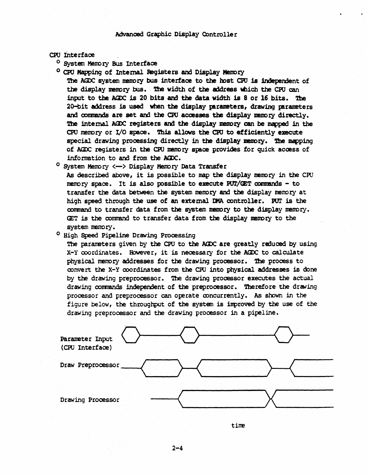
o High Speed
Pipeline
Drawing
P~cessing
The
paraneters
given by
the
CPU
to
the
ACJX;
are
greatly
reduced by using
X-y
ooordinates.
However,
it
is
necessary
for
the
Aa>C
to
calculate
physical
nenory
addresses
for
the
drawing
processor.
'!be
process
to
oonvert
the
X-Y (X)()rdinates from
the
CPU
into
physical
addresses
is
done
by
the
drawing
preprocessor.
'!be drawing
processor
executes
the
actual
drawing
ooImBnds
independent
of
the
preprocessor.
'1herefore
the
drcwing
processor and
preprocessor
can
oJ:erate
ooncurrently.
As srown
in
the
figure
below,
the
throughput
of
the
system
is
improved by
the
use
of
the
drawing
preprocessor
and
the
drawing
processor
in
a
pipeline.
Paranete
r
Input
(CPU
Interface)
~~p~ro~sor
__
~<
___
~~~
______
~)~~~<
____
_
Drawing Processor
tine
2-4
Advanced Graphic Display
Controller
2.2
Q:mmond/Pargete r Exc;hange
Between
.tl:&
a!l
.IDd
~
It
is
necessary
for
the
CPU
to
set
various parametem
and
ooammds
to
operate
the
drawing
and
display
oontrol
functions
of
the
AaX..
'lb
set
these
plraneters
and
Q)nm:mds,
the
CPO
writes
them
directly
to
the
NZJC
intemal
registers.
'nle
internal
registers
of
the
ND:
can
be
classified
into
registers
the
CPU
can
read and
write
directly
and
registers
in
which
reaiing
or
writing
is
prohibited.
'nle
registers
which can
be
read
and
written
are
assigned
unique
addresses.
'1tley
are
mapped
in
the
CPU
nent>ry
or
I/O
Splce and
referred
to
as
the
'(X)rrmand/paraneter
table'.
'lbese
registers
are
selected
by
the
lower 8
bits
(OOB
-
FFH)
of
the
address
input
on
MADO
-
MNJ7
to
the
AaX:,
when
CSIR
is
low. '!be
data
to
be
read
or
written
can be
sent
through
the
data
bus
in
the
sane
address
cycle
providing
high speed
comrcand
or
parameter exchange.
The
Ar:D::.
inoorporates
a
preprocessor
for
drawing
preprocessing
and
a drawing
processor
for
the
actual
drawing. '!be drawing
preprocessor
calculates
the
effective
(physical)
address
from
X-Y
cx>ordinates
(logical
address) given
by
the
CPU
and
generates
the
parameters
of
the
micro-level
CX>des
intetpretErl
by
the
drawing
processor.
'!be drawing
preprocessor
decodes
CXI'IItlaMs
and performs
the
drawing
preprocessing
necessary
to
execute
ex>nmmds
in
the
cx>mmmd/
paraneter'table.
It
is
not
necessary
to
write
all
the
paraneters
in
the
oorrm:md/parameter
table.
Cnl.y
the
required
paranetets
for
the
particular
command
need be
written.
Of
the
addresses
OOH
-
FFH
in
the
intemal
register
space,
80H
-
FFH
are
not
presently
used. These
are
reserved
for
future
use.
'!be
register
addresses
OOH-7FH
can be grouped
into
four
categories
as
shown
in
the
following
table.
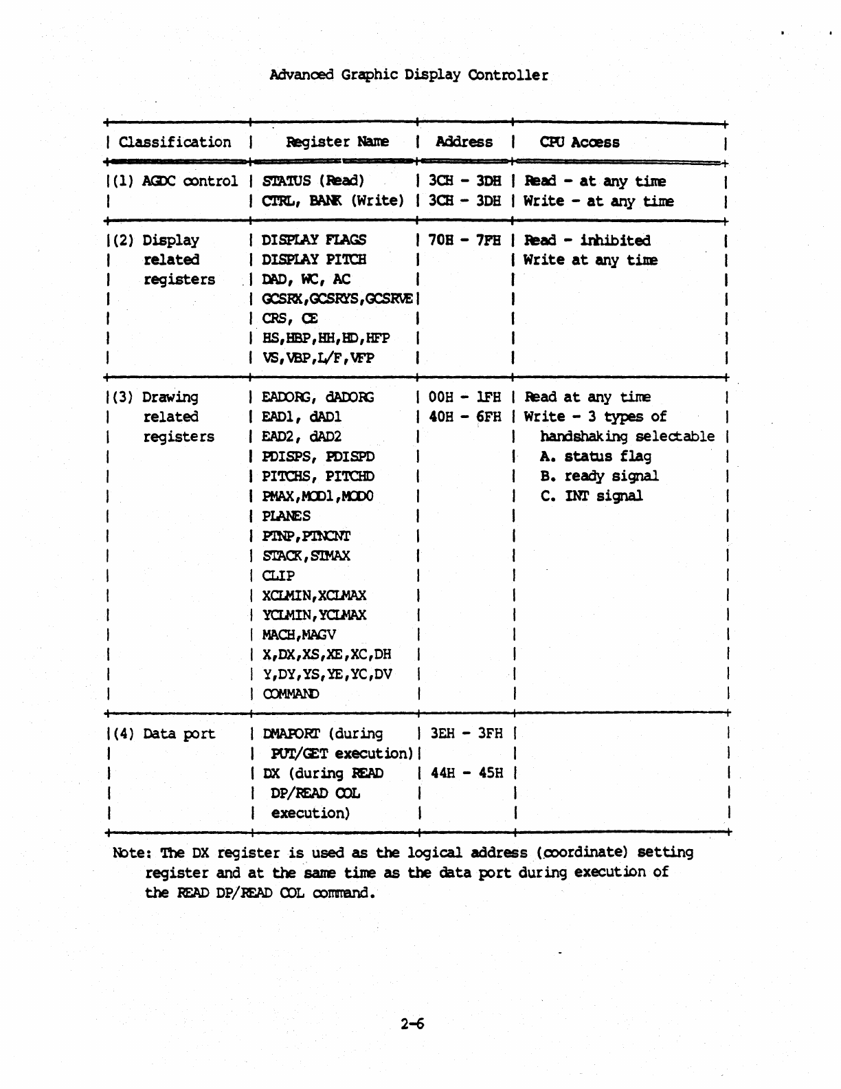
2-5
Advanced Graphic
Display
Controller
I
Classification
Register
Name
Address
CPO
Access
1(1)
1GX:,
oontrol
I
STA'lUS
(Read) I 301 -
30B
I
Read
-
at
any
tine
I I
Cl'RL,
IWt{
(Wr
ite)
I
3aI
-
3DB
I
Write
-
at
any
tine
I (2)
Display
I
DISPLAY
FIAGS
I 708 -
7PH
I R!ad -
inhibited
I
related
I
DISPIAY
PI'lCB I I
Write
at
any time
I
registers
. I
IW>,
le,
AC
I r
I I
OCSRK,GCSRlS
,GCSRVE
I I
I I
CRS,
CE
I I
I I
BS,HBP
,HH,BD,HFP
I I
I I
VS,VBP,I/F,VFP
I I
I (3) Drawing I FAro:£(;, dAIX)R:; I
OOB
-
lFB
Raad
at
any
tim:
related
I tADl,
dADl
I
40B
-
6FH
I
Write
- 3 types
of
registers
I
EAD2,
dAD2
I
hanlshaking
selectable
I PDISPS,
PDISPD
J A.
status
flag
I PI'1':HS,
PlroID
J B. ready
signal
I
PMAX,
MDl
,ftD)()
I C. IN.I'
signal
I
PIANES
I
I
PmP,
P.LN:NI'
I
J
STACK,
S'IMAX
I
I CLIP I
I
XCIlUN,XCI.MAX
I
f
YCl.MIN,
YCIl-W{
I
I
MACH
,l-lAGV
I
I
X,DX,XS,XE,XC,DH
I
I y,DY,yS,YE,yC,OV I
I
CDMMAID
I
I (4)
Data
port
I IlWORr
(during
3EH
-
3FH
I
I I
PUl'/CET
execution)
I I
I I
OX
(during
W.AD
I
44H
-
4sH
I
I I DP/lEAD
CX>L
I I
J I
execution)
I I
N:>te:
The
OX
register
is
used
as
the
logical
address
(.CX)()rdinate)
setting
register
and
at
the
same time
as
the
data
port
during
execution
of
the
READ
OP/WAD
CDL
oorme.nd.
2-6
I
I
I .
I
I
Advanced Graphic Display
Controller
1be
'registers
in
the
first
classification
-srA'lUS,
Cl'RL
and
BAR(
-
are
assigned
address
3CH
-
3DH.
'l!le
oontents
of
the
STA'lUS
register
can
be
reeD
at
any
tine.
'!be
Cl'R[,
and
BARt
registers
can
be
written
to
by
the
CPU
at
any ,
tine.
'!be
registers
in
the
seCX)m
group -
display
related
registem
-
are
assigned
addresses
in
the
range
70B
-7Fa. '!he CDntents
of
these
registers
cannot be
read.
Data
can be
written
to
these
registem
at
any
tine.
Ibweve~,
writing
to
these
registers
can
disturb
the
CRl'
display.
To
prevent
this,
the
display
can
be blanked
while
writing
to
these
registers.
First
set
the
S)
bit
in
the
DISPIAY FlAGS
register
(address 70B-7lB)
to
'1'.
Sea:>nd,
write
the
data
into
the
display
related
register
group.
'!bird,
set
the
SJ
bit
from
'1'
back
to
'0' •
Follow
these
procedures
to
write
data
(SYH:
parametets) such
as
SS,
HBP,
HE,
HO,
HFP,
VS,
VBP
and
!IF
on
the
registers
at
"address
7EH
-
7FB:
1.
Set
the
SYN:
bit
in
the
DISPIAY
FIAGS
register
(70H
-7lH)
to
'1'
2.
Write,
in
the
order
listed,
SS,
BBP,
HH, HO,
BFP,
VS,
VBP,
I/F
AN)
VFP
(address
7EH
-7FH).
3.
Set
the
SYNC
bit
to
'0'
The
registers
in
the
drawing
related
group
are
assigna:i
addresses
from
OOH
to
lFE and
40H
to
6FH.
The
preprocessor
resides
in
this
register
group. '!he
read/write
option
of
these
registers
are:
-aead
The
CPU
can read
the
contents
of
these
reg
is
te
IS
at
any
tine.
The
preprocessor
stops
for
one
clock
while
the
contents
of
a
register
are
read.
-Write
One
of
three
writing
procedures can be used:
1.
Check
the
STA'IUS
register
PPBSY
flag
(~dress
3CH)
2.
Use
the
READY
signal.
3.
Use
the
IN!'
pin
to
signal
an
interrupt.
to
the
au
The method
described
by (1)
is
the
general
nettOO.
'!he
contents
of
the
status
flag
are
read
to
check
that
the
preprocessor
is
not
in
operation.
If
the
preprocessor
is
not
busy,
then
data
can be
written
to
the
CCIt1lti1!ld/plrarreter
table.
In
the
method
described
by
(2),
the
au
is
tied
to
the
A(])c's
READY
line.
If
the
preprocessor
is
busy,
the
CPU
cannot
write
the
data
until
the
preprocessor
is
finished
and
the
READY
line
goes
high.
This procedure
enables
the
exmmand/pararreter
data
to
be
sent
at
a
higher
speed.
2-7
Advanced Graphic
Display
Controlle
r
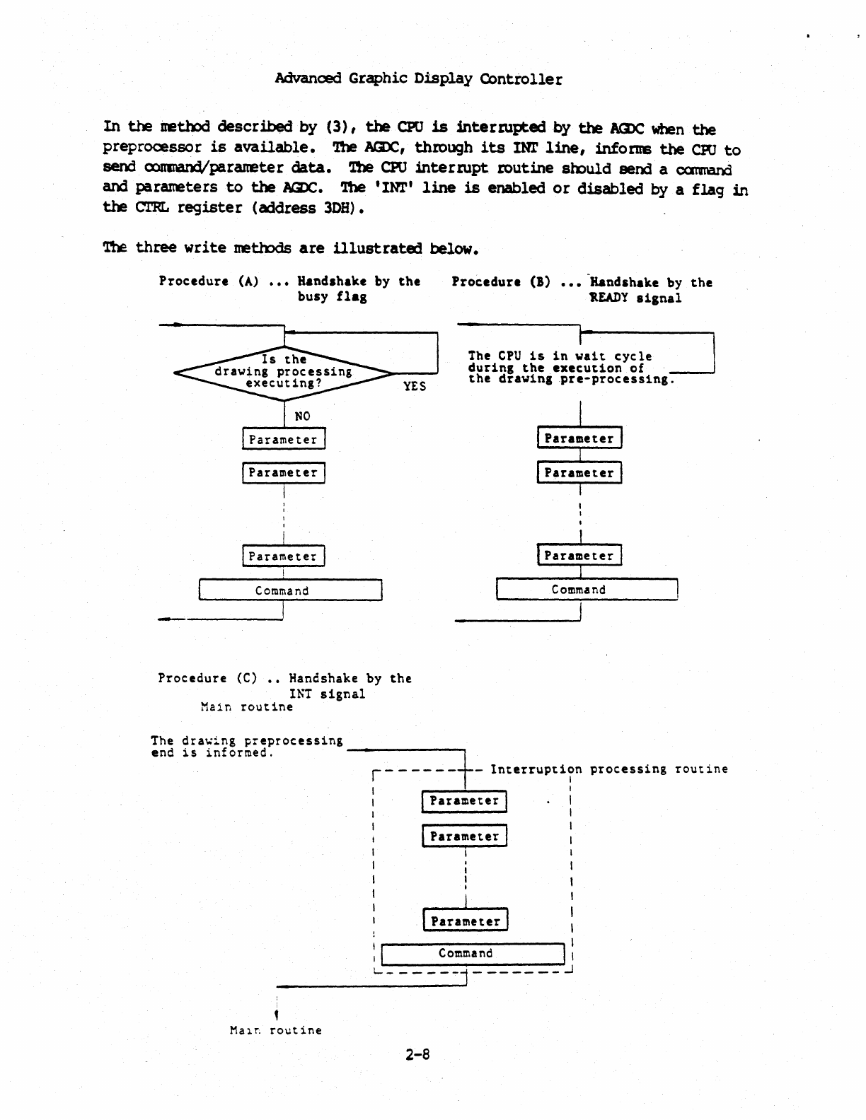
In
the
netb:>d
described
by
(3),
the
CPO
is
interNpted
,by
the
&CDC
when
the
preprocessor
is
available.
'!be
AaX:.,
through
its
IN!'
line,
inforns
the
au
to
send
cxmnand/paraneter
data.
The
CPU
interrupt
routine
srould
send a
CXIr1rt\aOO
and parameters
to
the
NZlC.
'!be'
INl"
line
is
enabled
or
disabled
by
a
flag
in
the
CTRL
register
(address
3OB).
'!be
three
write
meth:>ds
are
lllustrated
below.
Procedure
(A)
•••
Handshake by
the
busy
flag
Procedure
(I)
•••
-Handshake by
the
llEADY
Signal
I
Parameter
I
I
I
para~eter
I
I
YES
The
CPU
is
in
wait
cycle
during
the
execution
of
the
draw1nlpre-process1ng.
Command
Procedure
(C)
••
Handshake by
the
IN!
signal
Main
routine
!he
dra~ing
preprocessing
end
is
informed.
-------,t
r - - - - - - -
Interrupti?n
pl'ocessing
rout
ine
I I
I I
Parameter
I :
I
Parametel'
I :
I
I
Parameter
I
: I
Command
I :
_----L--------------'1 - - - - - - -
.J
MalT;
routine
2-8
Advanced Graphic
Display
Controlle
r
'nle
data
port
register,
~Rr,
is
at
address
3Ea
-3F8. '!he drawing
processor
uses
this
register
during
execution
of
the
drawing
preprocessing.
'1berefore,
to
read/write
this
register,
follow
the
uetb:>d
for
reading
or
writing
the
drawing
prep~ssor.
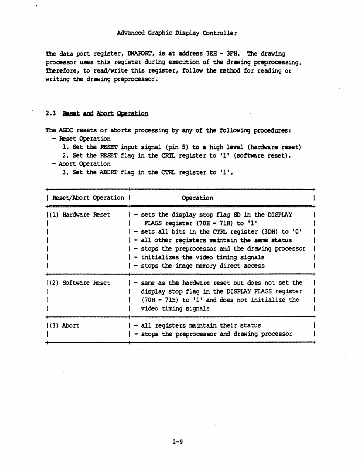
2.3
BIBt
ADd.
6tQ.G Qgeratioo
The
AfZX:,
resets
0 r
abo
rts
processing
by any
of
the
following
procedures:
-Reset Operation
1.
Set
the
RESET
input
signal
(pin
5)
to
a high
level
(hamware
reset)
2.
Set
the
~SET
flag
in
the
am:,
register
to
'1'
(sofbBre
reset).
-Abort
Operation
3.
Set
the
~RI'.
flag
in
the
CTR[.,
register
to
'1'.
Reset/Abort
Operation
1(1)
Hardware
~set
I
I
I
I
I
I
1(2)
Software
~set
1
I
I
I
(3)
Abort
I
Operation
-
sets
the
display
stop
flag
S)
in
the
DISPIAY
FIAGS
register
(70R -
71B)
to
'1'
-
sets
all
bits
in
the
~
register
(3DH)
to
'0'
-
all
other
registers
maintain
the
same
status
-
stops
the
preprocessor
and
the
drawing
processor
-
initializes
the
video timing
signals
-
stops
the
l.nege nenory
direct
access
-
same
as
the
hardware
reset
but
Cbes
not
set
the
display
stop
flag
in
the
DISPIAY
FLAGS
register
(70H -71H)
to
'1'
and Cbes
not
initialize
the
video timing
signals
I -
all
registers
mintain
their
status
I -
stops
the
preprocessor
and drawing
processor

Advanced
Graphic Display
Controller
2-10
Advanced
Graphic Display Controller
Section
3
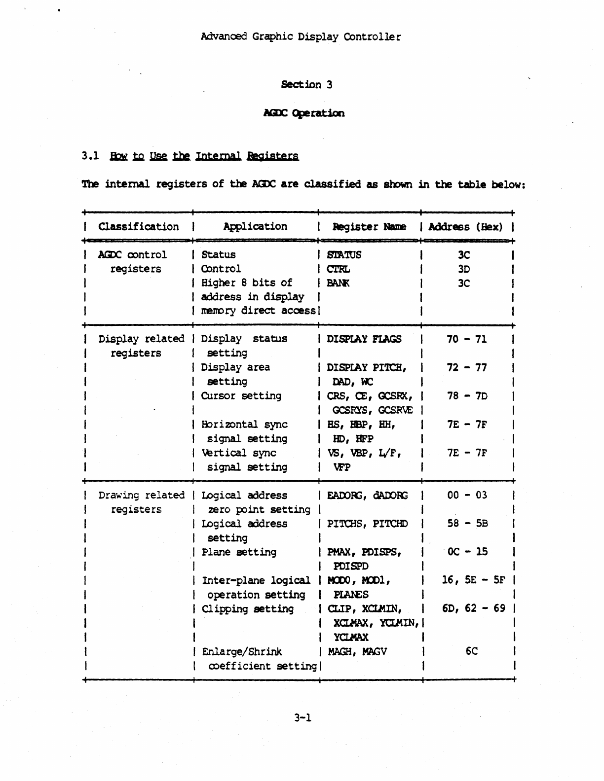
3.1
B14
m
12K
tbl
Intemal
Resisters
The
internal
registers
of
the
laX:
are
classified
as
smwn
in
the
table
below:
Classification
ItfZ'£
c:x>ntrol
registers
Display
related
registers
Dra~'ing
related
registers
AWlication Register
Nue
I Address (Hex)
~t~
I
~~S
I Q)ntrol I
CTRL
I Higher 8
bits
of I
BAR<
I address
in
dis,play I
I
memory
direct
access I
I Display
status
DISPIAY
FlAGS
I
setting
I Display area
DISPIAY
PI'lCH,
I
setting
Dt\D,
lC
I Cursor
setting
CRS,
CE,
GCSRX,
I
GCS~,
GCSRVE
I B:>rizontal sync BS,
BBP,
HH,
I
signal
setting
HO,
BFP
I
~rtical
sync
VS,
VBP,
L/F,
I
signal
setting
VFP
IDgical address I
EAIX)R:2,
dAlX)R:;
zero point
setting
I
wgical
address I
PITCHS,
PITCHD
setting
I
Plane
setting
I
PMAX,
PDISPS,
I
PDISPD
Inter-plane
logical
I KDO,
KDl,
operation
setting
I
PWES
Cl
ipping
setting
I
CLIP,
XCU'lIN,
I
XQIU\X,
YQlt1IN,
I
YCI.HAX
Enlarge/Shr ink I
MAGS,
MAGV
coefficient
setting
I
3-1
3C
3D
3C
70
-
71
72
-
77
78
-
7D
7E
-
7F
7E
-
7F
00 -03
58
-
5B
OC
-
lS
16,
SE
-
SF
6D,
62
-
69
6C
Advanced
Graphic
Display
Controlle
r
Classification
AJ;plication
Register
NIUIe
I Address (Hex)
Drawing
related
Painting
pattem
I PlNP, PnCN.r 18-lA,6G-61
registers
setting
(
mntinued)
JaY:,
work
area
set
sma,
S'l'MAX
le-lE,SC-50
Pbysical
address
IADl,
EAD2
04-06,OS-oA
(word
addr)
value
setting
Physical
address
dADl,
dAD2
07,
OB
(mt
addr.)
value
setting
IDgical
address
(X
*
X,
DX
, XS,
D,
40
-
S5
coord.)
value
set
XC,
DB
IDgica.l
address
(Y
Y,
DY,
YS,
YE,
42
-
57
cx>ord.)
value
set
!C,
DV
Conrnand
CD1MAN)
6E
-
6F
I
Data
port
I Data
port
during
IIJWORl'
3E
-
3F
I
execution
of
Pt1l'/GET
I
I
Data
port
during
IOX*
44
-
45
I
execution
of
READ
I
I
OP/H:.AD
CXL
I
*:
'!be
DX
register
is
used as
the
logical
address
(X
coordinate)
value
setting
register
and
at
the
saIre
tine
as
the
data
port
during
the
execution
of
a
m'AD
OP/READ
CXlL
oonrrand.
3-2
Advanced
Graphic
Dis~ay
Controller
3.2-
~
Qlntrol
Registers
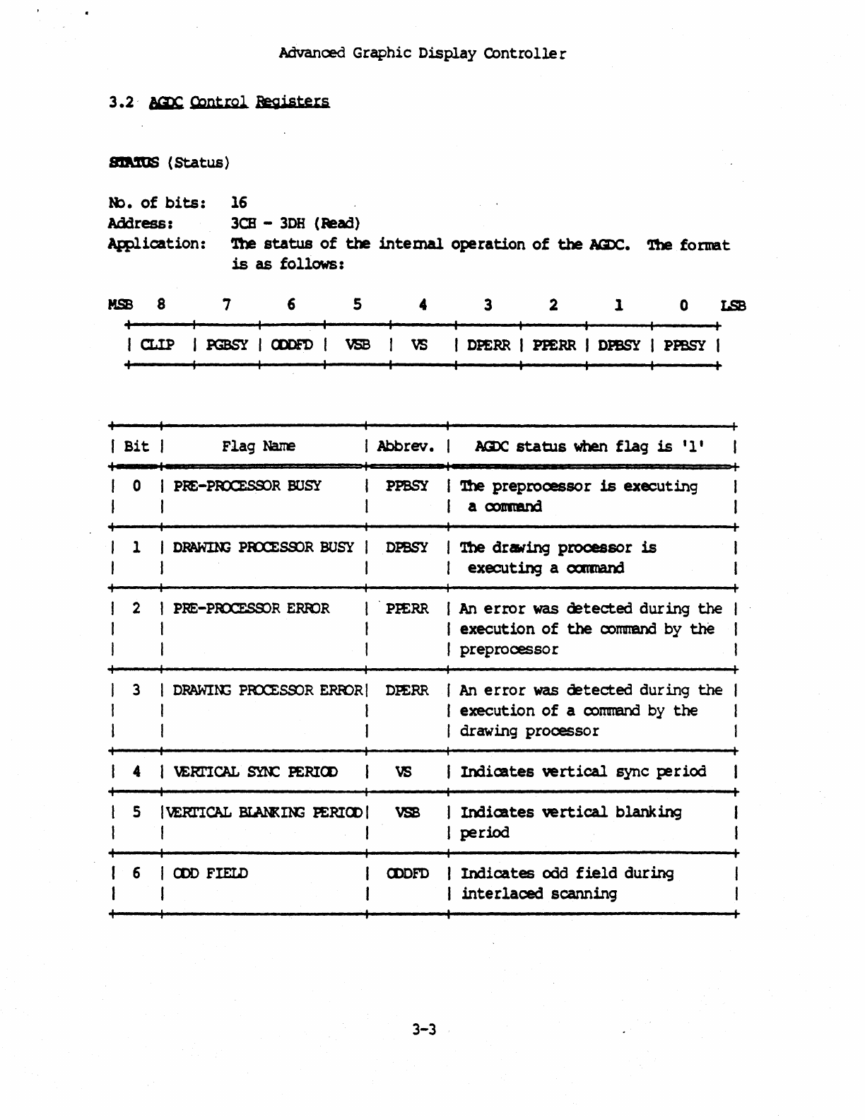
BJUUS
(Status)
H:>.
of
bits:
16
Address:
3CB
-
30B
(Read)
ARUication:
'lhe
status
of
the
intemal
operation
of
the
1aX:,.
'!be format
is
as
follows:
MSB
8 7 6 5 4 3 2 1 o
LSB
I
CUP
I
PGBSY
I cmFD I
VSB
vs
I
DPERR
I
PPERR
I
DPBSY
I
PPBSY
I
I
Bit
Flag
Narre
I Abbrev. AmC
status
when
flag
is
'l'
0 I PF£-PR:Q8&)R
BOSY
PPBSY
I
1M
preprocessor
is
executing
I I a
COJIItIU'X3
1 I
DRAWm:;
PRXESS:>R
BUSY
I
OPBSY
I
1be
drwing
processor
is
I I I
executing
a
CX'IIIDal'd
2 I
PRE-PlO:!ES&:>R
ERR:>R
PI£RR I
An
error
was
detected
during
the
I I
execution
of
the
oomnand
by
the
I I preprooesso r
3 I
OPAWIN3
PRX'ESSOR
ERK>RI
DI£RR I
An
error
was
detected
during
the
I I I
execution
of
a
co~
by
the
I I I drawing
processor
4 I
VERI'ICAL
sm: PERIa>
VS
Indicates
vertical
sync
period
5 I
VERl'ICAL
BIAtl{nt;
PERICD
I
VSB
I
Indicates
vertical
blanking
I I I period
6 I
CDD
FIEID
CDDFD
Indicates
odd
field
during
I
interlaced
scanning
3-3
Advanced
Gr~hic
Dis~ay
Controller
Status
(cx:>ntinued)
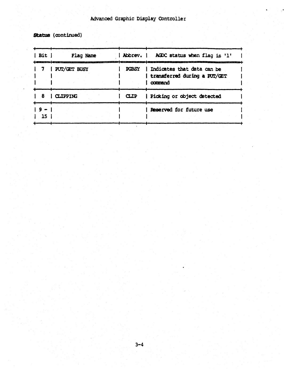
1
Bit
J
Flag
Name
7 I PUr/GET
BUSY
I
I
8 1 CUPPIK;
19-1
I lS I
I
Abbrev.
NZX:.
status
when
flag
is
'1'
PGBSY
I
Indicates
that
data
can
be
I
transferra:i
during a
POT/CZT
I
CDIIIBnd
CUP
I
Picking
or
object
detected
3-4
I Reserved
for
future
use
I
, .
..
(Bank)
1t>.
of
bits:
Address:
AWlication:
Advanced Graphic
Display
Control
Ie
r
8
3CB
(Write)
'!be
CPU
interface on
the
AaX: acmDDdates
2o-bit
addresses.
'!be
~
can address 32
!bytes
of
display
meuDty (24
bits).
When
the
CPO
addresses
display
Jl8Dl)ty
directly,
the
lower 16
bits
provided
by
the
CPO
(bits
0 - 15)
is
CDlbJ.ned
with
the
upper
8
bits
(bits
16-23)
of
the
IW«
register
to
form
the
2..oit
display
JDeltDty address.
3-5
Advanced Graphic Display
Controlle
r
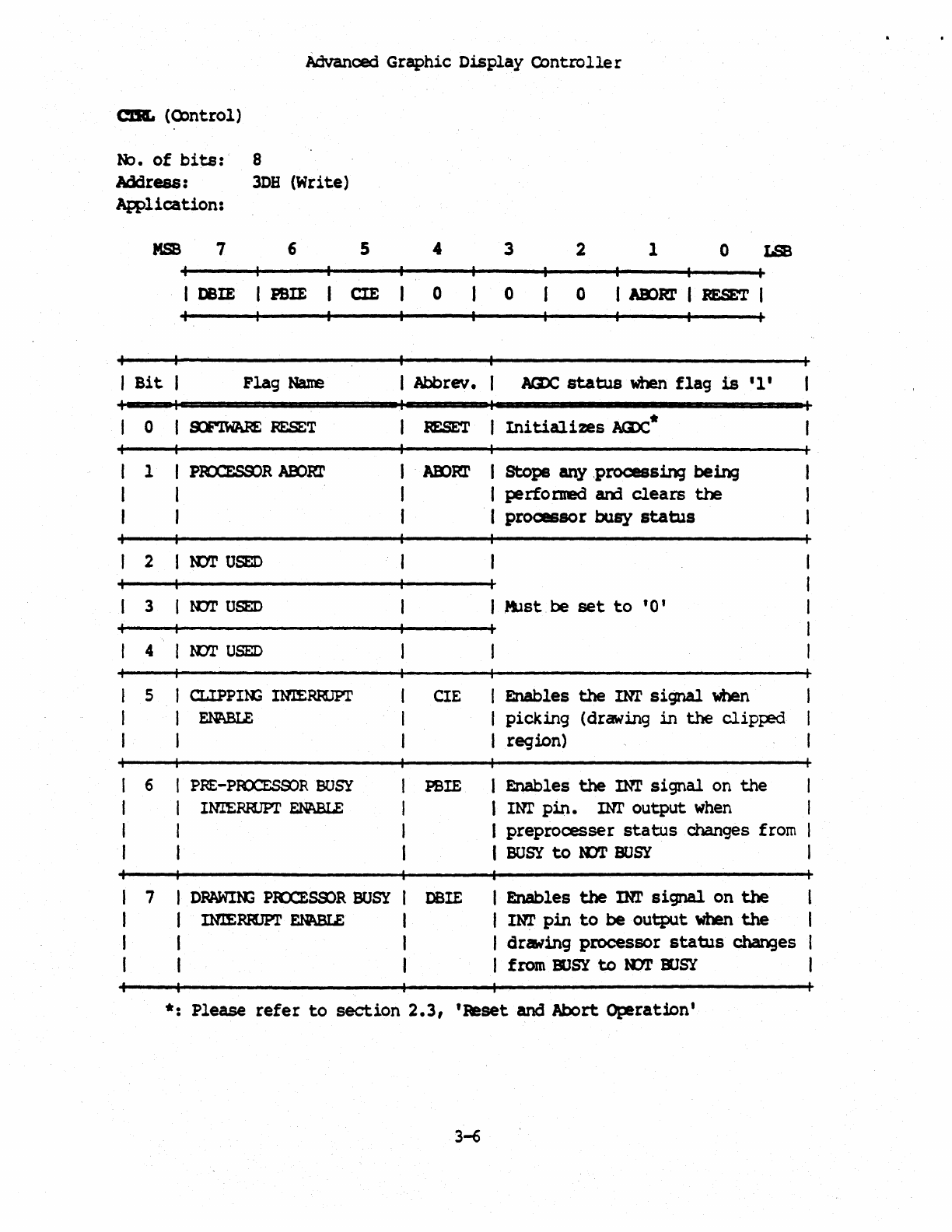
am. (OJntrol)
N::>.
of
bits:·
8
Address:
3DB
(Write)
AWlication:
MSB
7 6 5 3 2 1 o
LSB
I
DBlE
I PSIE
em
o o o I
ABlR1'
I
RESET
I
I
Bit
I
Flag
Na%re
I
Abbrev.
laX:.
status
when
flag
is
'1'
o I
s:FlWARE
RESET
1 I
P~R
AB:>Rl'
I
I
2 I N:n'
USED
3 I
N:Yr
USED
4 I
KYl'
USED
5 J CLIPPIt{'; INlERRJPr
I
EN1\BLE
I
6
PRE-PRXESOOR
BUSY
INrERRJPL'
EN1\BLE
Initializes
~*
AEDRl'
I Stope any ,processing
being
I performed
am
clears
the
I
processor
busy
status
I MJst
be
set
to
'0'
CIE I Enables
the
INI'
signal
trilen
I
picking
(drawing
in
the
clip~
I region)
PBIE I
Enables
the
INI'
signal
on
the
I IN!'
pin.
IN!'
output
when
I
preprocesser
status
changes from I
I
BUSY
to
RJI'
BUSY
I
7 I
DRAWIN:;
PRX:ESSOR
BUSY
I
OBIE
I Enables
the
IN!'
signal
on
the
I
Im'
pin
to
be
output
when
the
I INlERRJPr
EN1\BLE
I
I I
I I I drlWing
processor
status
chan3es
I from
BOSY
to
lCl'
ElJSY
*:
Please
refer
to
section
2.3,
'Reset
and Abort
Operation'
3-6
Advanced Graphic Display
Controlle
r
,
3.3
D!§glay
Belated
legiste
r
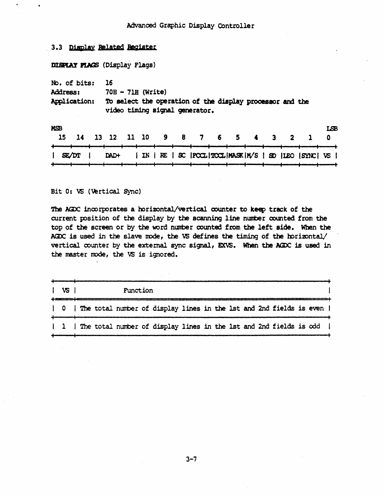
DISRAY
PUtGS
(Display
Flags>
~.
of
bits:
16
Address:
70B
-7lB (Write)
Application:
'1b
select
the
operation
of
the
display
processor
am
the
video
timing
signal
generator.
MSB
IS
14
13
12
11
10
9 8 7 6 5 4 3 2 1
LSB
o
I
SF/M
I IN
RE
s:
IPO:LI'ltCLIMASKlrvs
I
S)
IIEO
Ism:
I
VS
Bit
0:
VS
(vertical
Sync)
The
laX,
inoorporates
a
horizontal/vertical
CX)Ul\ter
to
keep
track
of
the
current
position
of
the
display
by
the
scanning
line
nlmber
ex>unted
from
the
'top
of
the
screen
or
by
the
word nurrber oounted from
the
left
side.
When
the
Aax:.
is
used
in
the
slave
node,
the
VS
defines
the
timing
of
the
h::>ri2Dntal/
vertical
oounter
by
the
external
sync
signal,
EKVS.
When
the
AGX:,
is
used
in
the
master
node,
the
VS
is
ignored.
vs
Function
+ o I
The
total
nurrber
of
display
lines
in
the
1st
and 2nd
fields
is
even
1 I
The
total
nurrber
of
display
lines
in
the
1st
and 2nd
fields
is
odd
3-7
Advanced
Graphic
Display
Controlle
r
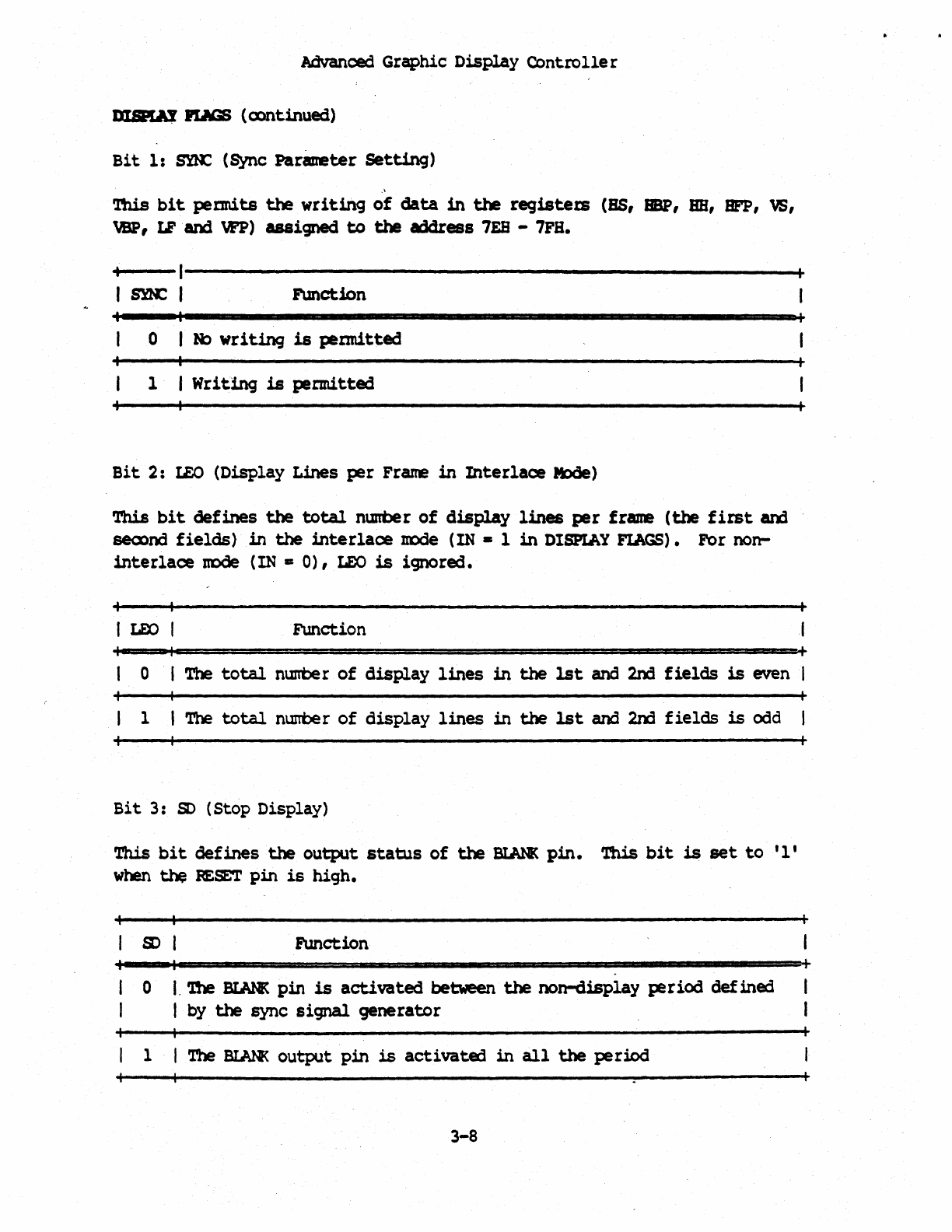
IJISIIAl
IUIGS
(CX)Ot1nued)
Bit
1:
sm: (Sync
Par_ter
Setting)
,\
'Ibis
bit
permits
the
writing
of
data
in
the
registem
(SS,
BBP,
RB,
BFP,
VS,
VBP,
LF
'and
VPP)
assigned
to
the
address
7EB
-
7FH.
+----1----------------------------------------------------+
I~I
Function
o
l!b
writing
is
pennitted
1 I Writ.ing
is
permitted
Bit
2:
LEO
(Display
Lines
per
Frame
in
Interlace
It>de)
This
bit
defines
the
total
nurrber
of
display
lines
per
frame
(the
first
arx1
seoond
fields)
in
the
interlace
DDde
(IN • 1
in
DISPIAY FlAGS). For non-
interlace
node
(IN
=
0),
LEO
is
ignored.
I
LEX>
I Function
o I The
total
nurrbe r
of
display
lines
in
the
1st
and 2nd
fields
is
even
1 I
The
total
nurrbe r
of
display
lines
in
the
1st
and 200
fields
is
cx1d
Bit
3:
SO
(Stop Display)
This
bit
defines
the
output
status
of
the
BlANK
pin.
'1'his
bit
is
set
to
'1'
when
the
~SET
pin
is
high.
Function
o
I.
'lb!
BlANK
pin
is
activated
between
the
non-display
period
defined
I
by
the
sync signal.
generator
1 I The BI.MI<
output
pin
is
activated
in
all
the
period
3-8
Advanced Graphic
Display
Controller
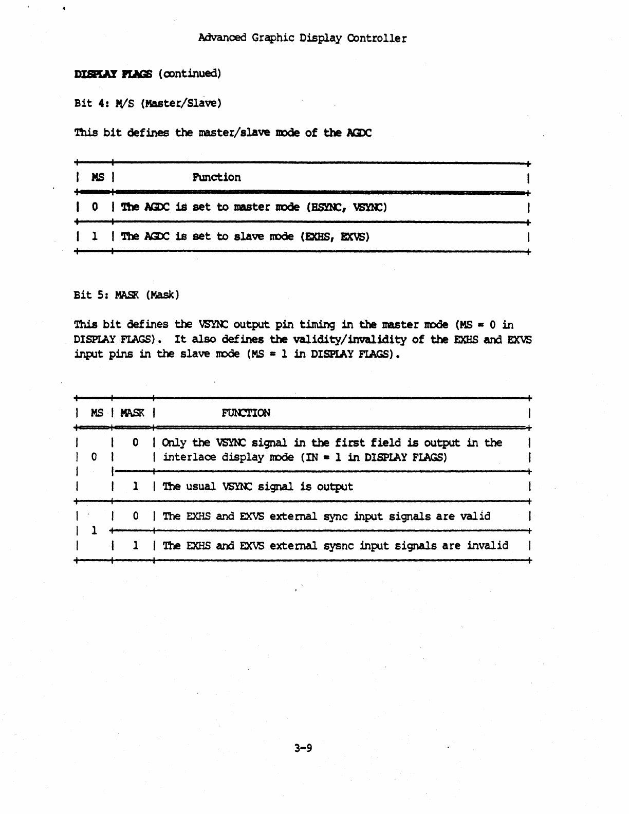
DUHAY
JUGS
(continued)
Bit
4:
MIS
(Master/Slave)
'l'his
bit
defines
the
master/slave
DDde
of
the
AGX
MS
Fwlction
o I
1be
NZJ;
is
set
to
master
DDde
(BSnC,
VEMC)
1 I
'nle
AGr,
is
set
to
slave
node
(EXHS,
EXVS)
Bit
5:
MASK
(Mask)
This
bit
defines
the
VSlR;
output
pin
timing
in
the
master
DOde
(MS
&:
0
in
DISPIAY
FIAGS).
It
also
defines
the
validity/invalidity
of
the
EXHS
and
EXVS
input
pins
in
the
slave
node
(MS
II:
1
in
DISPLAY
FIAGS).
MS
I
MASK
I +
o I Only
the
VSYN:
signal
in
the
first
field
is
output
in
the
o I
interlaoe
display
node
(m
• 1
in
DISPIAY
FIAGS)
1 I
The
usual
vsm:
signal
is
output
o I The
EXHS
and
EXVS
external
sync
input
signals
are
valid
1
+I----~----------------------------------------------~
1
The
EXHS
and
EXVS
extemal
sysnc
input
signals
are
invalid
3-9
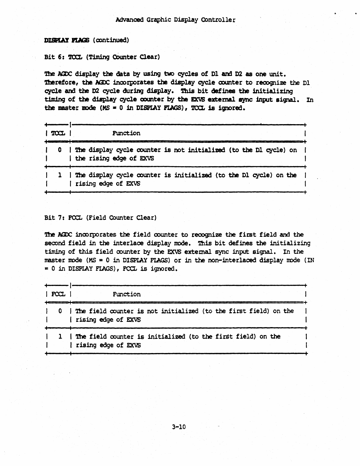
Advanced Graphic
Display
Controlle
r
DISL\Y
lUGS
(amtinued)
Bit
6:
'la:L
(Timing cOunter
Clear)
'l!le NZX:,
display
the
data
by
using two
cycles
of
Dl
and
D2
as
one
unit.
1mrefore,
the
lOX.
incorporates
the
display
cycle
oounter
to
recognize
the
Dl
cycle
and
the
D2
cycle
during
display.
1hls
bit
defines
the
initializing
timing
of
the
d1splay
cycle
counter
by
the
EXVS
extemal
sync
input
signal.
In
the
master
lOde
(MS
• 0
in
DISPlAY
FLAGS),
'ltXL
is
ignored.
+----I------------------------------------------~--------+
I
ro::L
I
Function
o I '!be
display
cycle
counter
is
not
initialized
(to
the
Dl
cycle)
on
I
the
rising
edge
of
EXVS
1 I
'1lle
display
cycle
oounter
is
initialized
(to
the
D1
cycle)
on
the
I
rising
edge
of
EXVS
Bit
7:
FCCL
(Field
CoW'lter
Clear)
'!be
IG:/:,
inoorporates
the
field
oounter
to
recognize
the
first
field
and
the
Sealnd
field
in
the
interlace
display
m:>de.
'!bis
bit
defines
the
initializing
timing
of
this
field
oounter
by
the
EXVS
extema!
sync
input
signal.
In
the
master
node
(MS
= 0
in
DISPIAY
FlAGS)
or
in
the
non-interlaced
display
IrOde
(IN
cOin
DISPIAY
FIAGS),
FCCL
is
ignored.
FCCL
Function
+===~c===================================================,+
o I
'1lle
field
oounter
is
not
initialized
(to
the
first
field)
on
the
I
rising
edge
of
EXVS
1 I '!be
field
oounter
is
initialized
(to
the
firSt
field)
on
the
I
rising
edge
of
EXVS
3-10
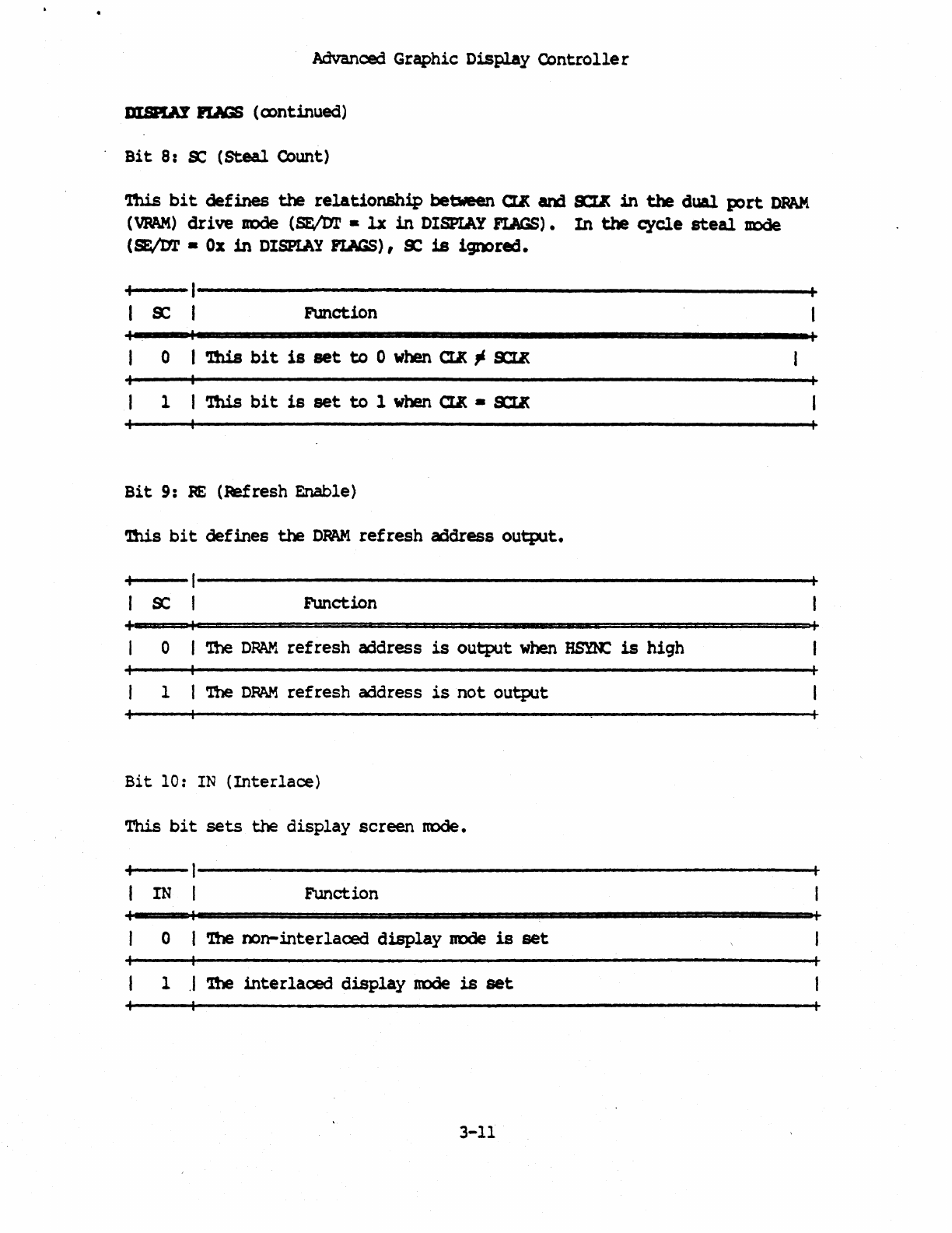
Advanced Graphic
Display
Controlle
r
IJISEI!AY
PLAGS
(oontinued)
Bit
8:
s:
(Steal
Count)
'lhi.s
bit
defines
the
relationship
between
Ql(
and
s:ut
in
the
dual
port
DPAM
(VRAM)
drive
node
(SE/M'
•
lx
in
DISPIAY FlAGS).
In
the
cycle
steal
IIDde
(SE/M'
•
Ox
in
DISPlAY
FlAGS), s:
is
ignored.
Function
o I
'!his
bit
is
set
to
0
when
Ql(
Jl
s::tJt
1 I rus
bit
is
set
to
1
when
aK
• s::tJt
Bit
9:
RE
(Refresh Enable)
1his
bit
defines
the
DRAM
refresh
address
output.
Function
o I
The
DRAM
refresh
address
is
output
when
HSYNC
is
high
1
The
D~
refresh
address
is
not
output
Bit
10:
IN
(Interlace)
This
bit
sets
the
display
screen
mode.
IN Function
o I '!he
non-interlaaad
display
JIDde
is
set
1
.I
'1be
interlaced
display
node
is
set
3-11
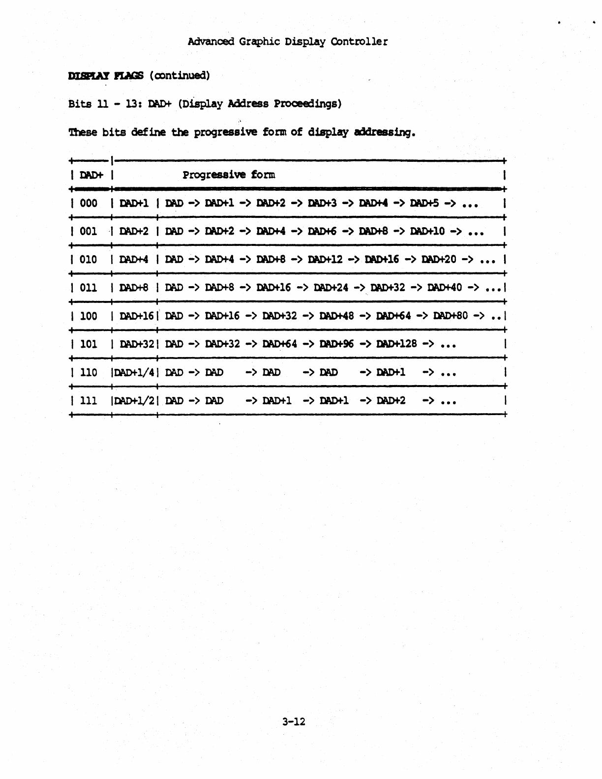
Advanced Graphic
Display
Controller
DImAY
PLAGS
(a>nt1nued)
Bits
11 -13:
~
(Display
Address Proceedings)
'1bese
bits
define
the
progressive
form
of
display
addressing
•
.----I------------------------------------------------~
I
Da\D+
I
Progressive
form
I 000 I
Dt\O+l
I
tN)
->
DPDt-l
->
Da\Of-2
->
Dt\D+3
->
DAD+4
->
IW>+5
->
•••
I
001
·1
DAD+2
I
Dt\D
->
DJ\I)f-2
->
DAD+4
->
1W>+6
-> IW>t8 ->
IW>+lO
->
•••
1
010
I
DAD+4
I
DAD
->
Dt\Df-4
->
IW>t8 ->
IW>t12
->
tw>+16
->
IW>t-20
->
•••
1011 I IW>t8 I
DAD
->
DAD+8
->
DAD+16
->
DAD+24
->,DAD+32
->
DAD+40
->
••• 1
1100 I
DAD+16f
DAD
->
Dt\Df-16
->
DAD+32
->
DAD+48
->
1W>+64
->
DAD+80
->
••
1
I
101
I
DAD+321
DAD
->
DAD+32
->
DAD*64
->
DAD+96
->
DAD+128
->
•••
I
110
1DAD+1/41
DAD
->
DAD
->
DAD
->
DAD
->
DAD+1
->
•••
I
111
1rw>+-l/21
DAD
->
DAD
->
Dt\D+1
->
IW>t-1
->
IW>+2
->
•••
3-12
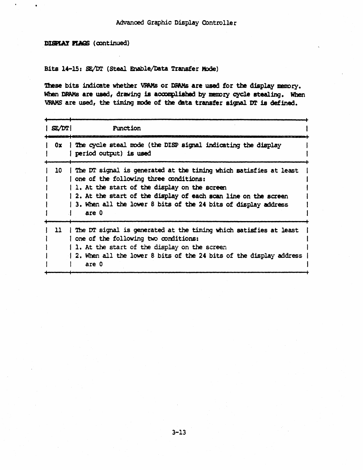
Advanced Graphic
Display
Controlle
r
IWHAY
lUGS
(alntinued)
Bits
14-15:
SE'/DT
(Steal
Enable/Data
Transfer
Jb:ie)
ibese
bits
indicate
whether
VMMs
or
DMMs
are
used
for
the
display
DBl'Dry.
When
DMMs
are
used,
drawing
is
accxmpliahed
by
1lleDl)J:Y
cycle
stealing.
When
VPAMS
are
used,
the
timing
node
of
the
data
transfer
8ignall71'
is
defined.
I
SE'/DTI
Function
Ox
I
1be
cycle
steal
Jll)de
(the
DISP
signal.
indicating
the
display
I
period
outplt)
is
used
10 I
The
M'
signal
is
generated
at
the
timing
which
satisfies
at
least
I one
of
the
following
three
mndi
tions:
I
1.
At
the
start
of
the
display
on
the
screen
I
2.
At
the
start
of
the
display
of
each
scan
line
on
the
screen
I
3.
When
all
the
lower 8
bits
of
the
24
bits
of
display
address
I
are
0
11 I '!be
M'
signal
is
generated
at
the
timing
which
satisf
ies
at
least
I one
of
the
following
b«>
oomitions:
I
1.
At
the
start
of
the
display
on
the
screen
I
2.
When
all
the
lower 8
bits
of
the
24
bits
of
the
display
address
I
are
0
3-13
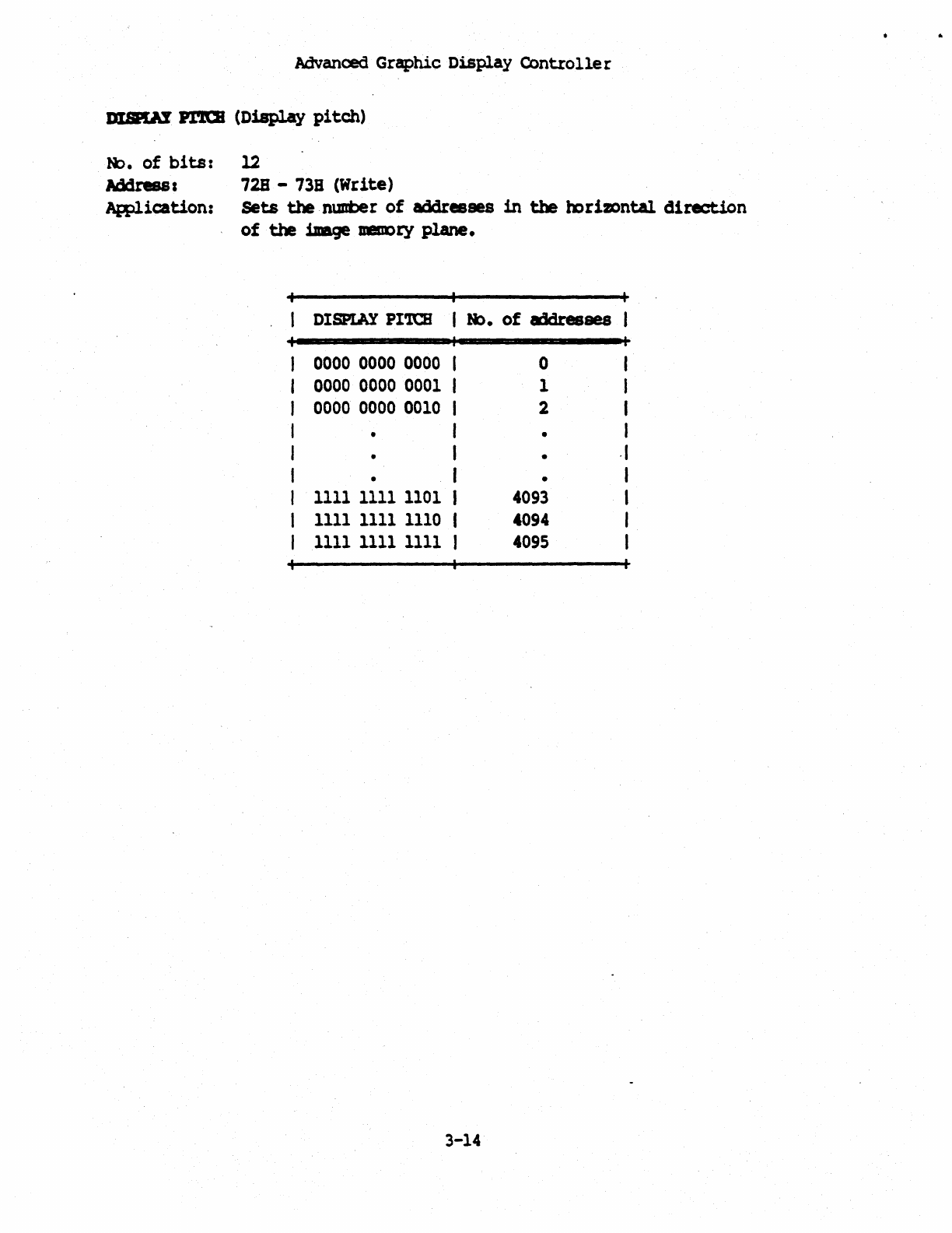
Advanced Graphic
Display
Controlle
r
DISlU.Y Pl'.laI (Display
pitch)
!t>.
of
bits:
Address a
Application:
12
728 -738 (Write)
Sets
theJlUllber
of
addresses
in
the
mrimntal.
direction
of
the
image
JDI!III)ry
plane.
DISPIAY
PI'laI
I
R:>.
of
Iddresaes
0000 0000
0000
I 0 I
0000 0000 0001
I 1 I
0000
0000
0010
I 2 I
• I • I
• I •
·1
• I • I
1111 1111
1101
I
4093
I
1111 1111
1110
I
4094
I
1111
1111
1111
I
4095
I
3-14
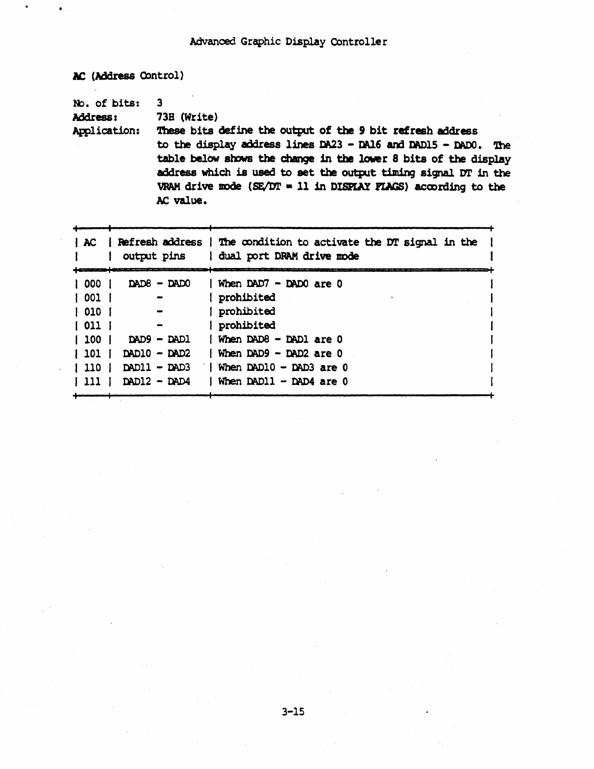
Advanced Graphic
Display
Controller
Ie
(Address
Olntrol)
~.
of
bits:
3
Address:
73B
(Write)
Application:
'Dlese
bits
define
the
output
of
the
9
bit
refresh
address
to
the
display
address
lines
Dt\23 -Dt\l6
and
Dt\D15
-
Jli\DO.
'!he
table
belOw
sh:Jws
the
change
in
the
lower
8
bits
of
the
display
address which
is
used
to
set
the
output
timing
signal
In'
in
the
VRAM
drive
lOde
(SF/M'
• 11
in
DISHAY
FIAGS)
ACQ)raing
to
the
AI:, value.
I
AC
I
Refresh
address
I '!be
a>ndition
to
activate
the
M'
signal.
in
the
I I
outplt
pins
I
dual
port
DPAM
drive
IIDde
I
000
I
I 001 f
I 010 I
I
011
I
I
100
I
I
101
I
I
110
I
I
111
I
Dr\D9
-
DADl
IY\DIO
-
Dt\D2
IW>11
-
Dt\D3
Df\D12
-
IW>4
I
When
DMfl
-
Dt\DO
are
0
I
prohibited
I
prohibited
I
prohibited
I
When
IW)8
-
IWll
are
0
I
When
DAD9
-
DAD2
are
0
- I
When
IY\DIO
-
Dt\03
are
0
I
When
IY\Dll -
MD4
are
0
3-15
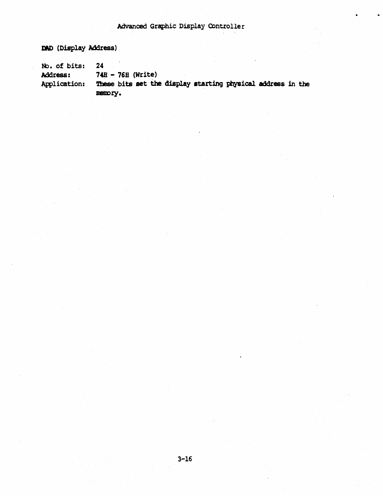
Advanced Graphic
Display
Controlle
r
JW)
(Display
Address)
R:>.
of
bits:
24
Address:
7411
-768 (Write)
AR;>lication:
'1bese
bits
set
the
display
starting
PtYsical
address
in
the
DBrDry.
3-16
..
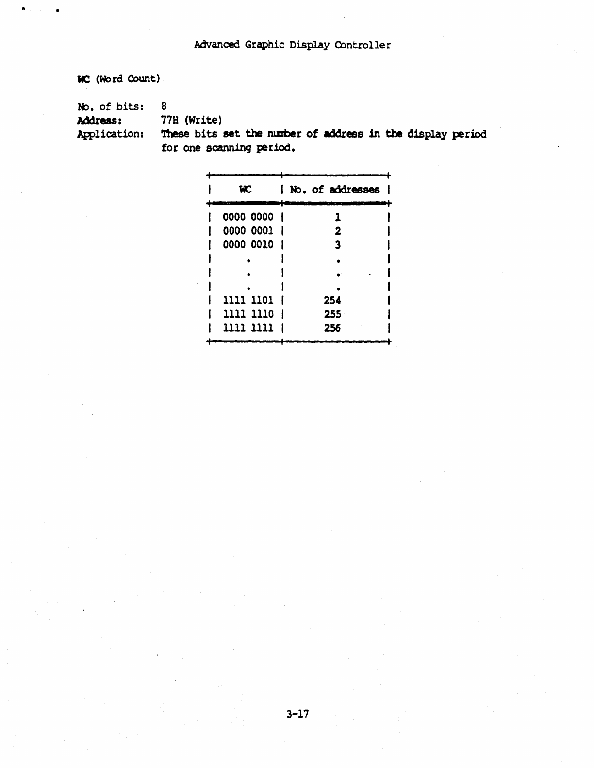
• •
Advanced Graphic
Display
Controlle
r
Il:
(Word
Count)
li:).
of
bits:
8
Address:
77H
(Write)
J.t:p1ication:
These
bits
set
the
ntmber
of
address
in
the
display
period
for
one scanning
period.
w:
I R>.
of
addresses
0000 0000
1
0000
0001
2
0000
0010
3
• •
•
• •
1111
1101
254
1111
1110
255
1111 1111
256
3-17
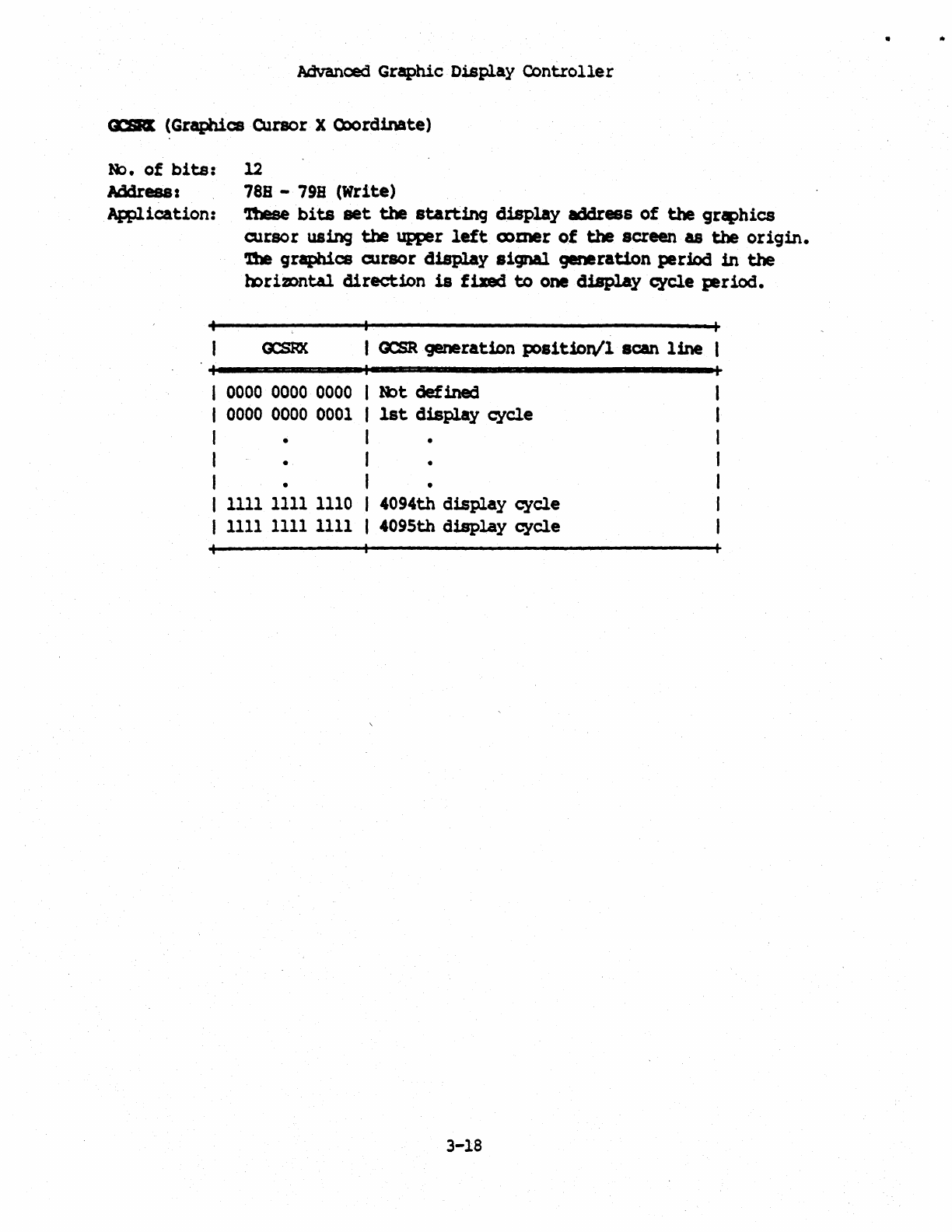
Advanced Graphic
Display
Controller
~
(Graphics Cursor X OX>rdinate)
R>.
of
bits:
12
Address I
ARllication:
78S
-
79B
(Write)
'ltlese
bits
set
the
starting
display
address
of
the graphics
cursor using the upper
left
c»mer
of
the
screen
as
the
origin.
-n.
graphics
cursor
d1splay
signal
generation
period
in
the
b:>rimntal
direction
is
fixed
to
one
d1splay
cycle
J;eriod.
I
0000
0000 0000
I
0000
0000
0001
I •
I •
I •
I
1111
1111
1110
I
1111 1111
1111
I
OCSR
generation
pos1t1orV1 scan
line
I
R>t
defined
I
1st
display
cycle
I •
I •
I •
I 4094th
display
cycle
I 4095th
display
cycle
3-18
•
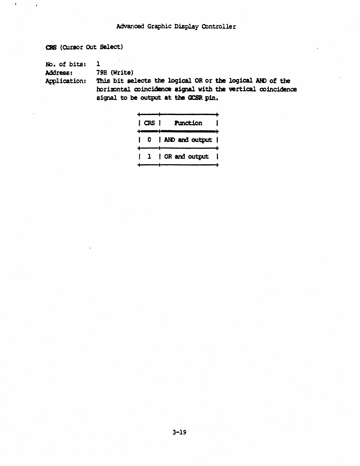
Advanced Graphic
Display
Controlle
r
.
cas
(CUrsor
OUt
Select)
~.
of
bits:
Address:
Application:
1
79B
(Write)
nus
bit
selects
the
logical
OR
or
the
logical
AM>
of
the
hori2Dntal
(X)incidenoe
signal
with
the
vertical
coincidence
signal.
to
be
output
at
the
crSR
pin.
I
OS
I Function
o I
Ali)
and
output
I
1 I
OR
and
output
3-19
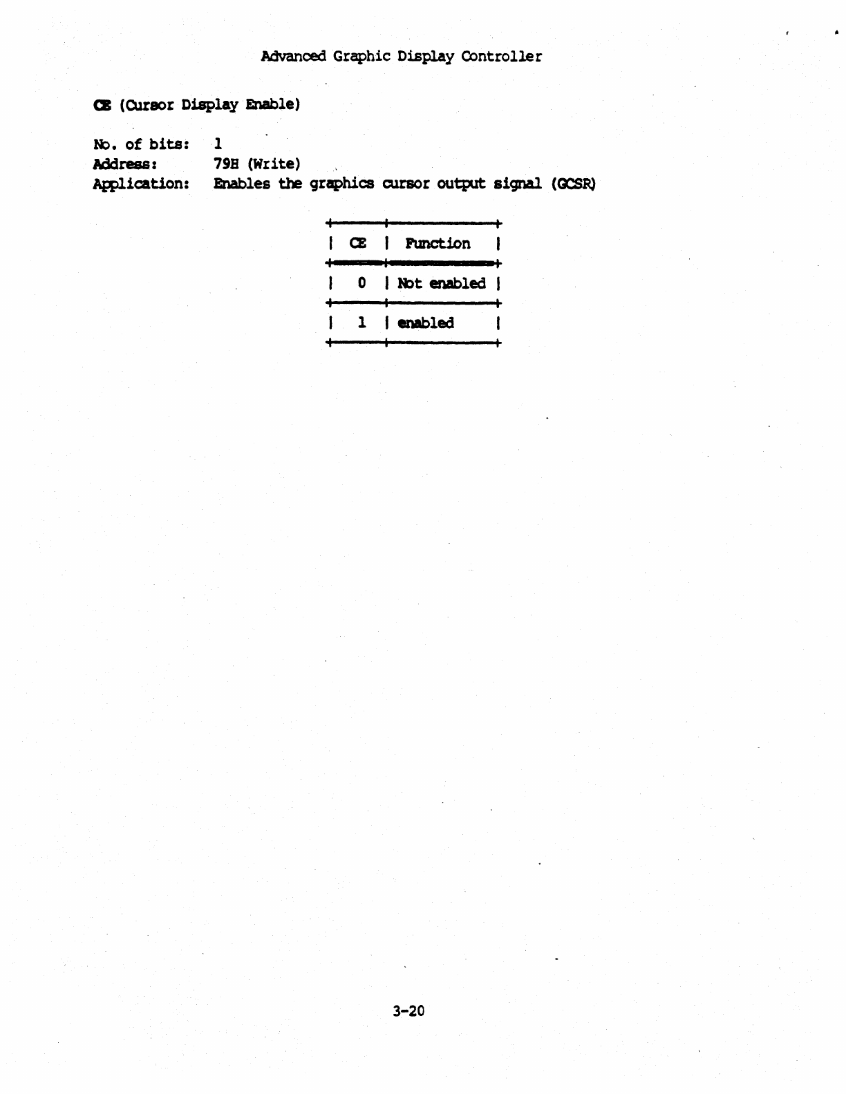
Advanced Graphic
Display
Controller
cz
(cursor
Display
Enable)
R>.
of
bits:
1
Address:
79B
(Write)
Application: Enables
the
graphics
cursor
output
signal
(~R)
CE
Plmction
o I
tbt
enabled
I
1 I
enabled
3-20
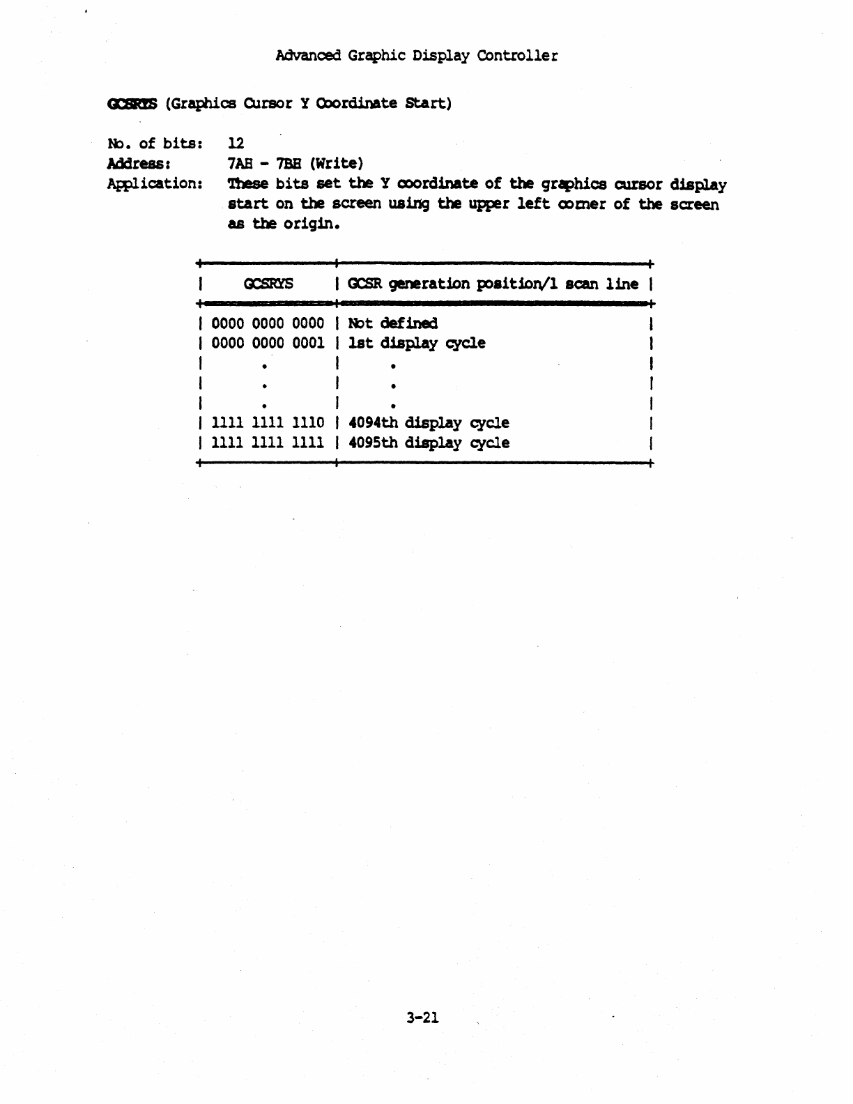
Advanced Graphic
Display
Controlle
r
Q&dS
(Graphics CUrsor Y Coordinate
start)
Rl.
of
bits:
Address:
~ication:
l2
7AB
-
7BB
(Write)
'lbese
bits
set
the
Y CX)()rdinate
of
the
graphics
cursor
display
start
on
the
screen using
the
upper
left
tomer
of
the
screen
as
the
origin.
I
OCSR
generation
poait1on/l
scan
line
I
0000
0000 0000
I
Nbt
defined
I
0000
0000
0001
I
1st
dis~y
~e
I • I •
I • I •
I • I •
I
1111
1111
1110
I 4094th display cycle
I
1111
1111 1111
I 409Sth
d~lay
cycle
3-21
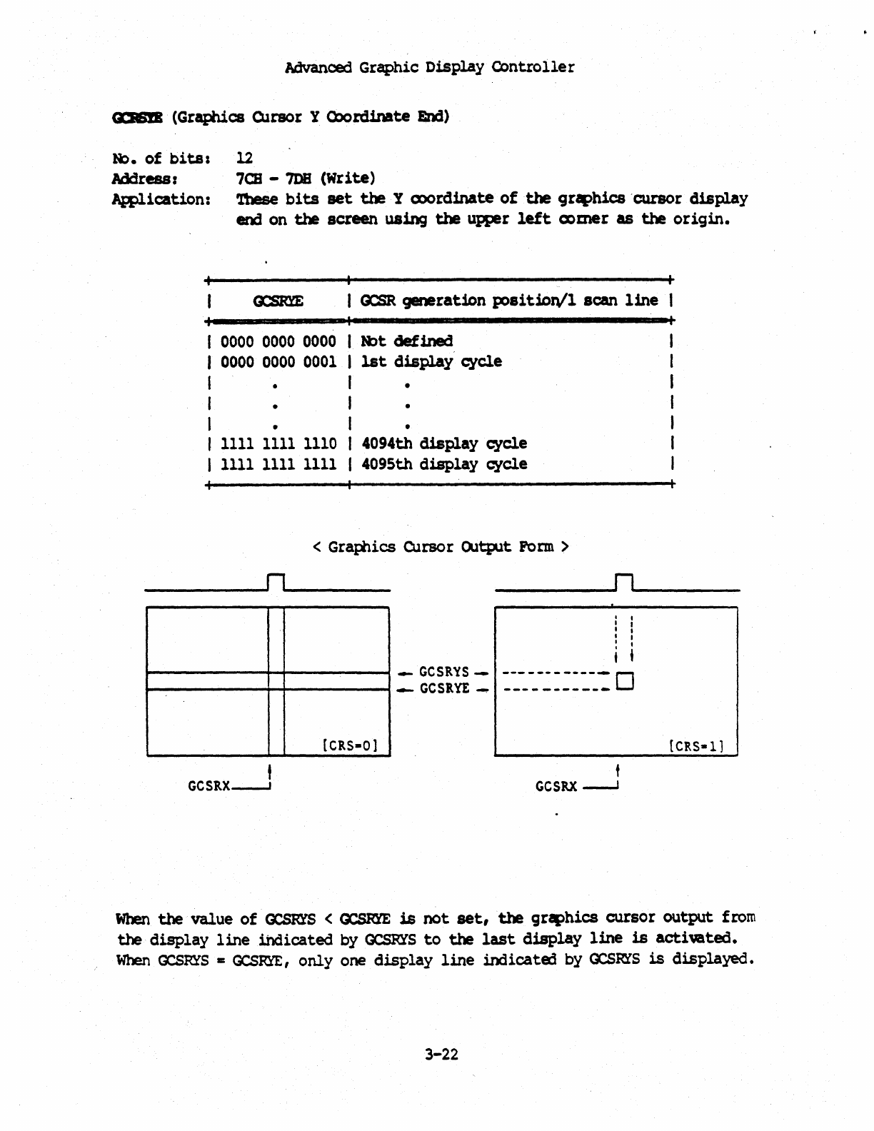
Advanced Graphic
Display
Controller
\U6iB
(Graphics CUrsor Y
Q)ordinate
End)
N:>.
of
bits:
12
Address:
7CB
-
7DB
(Write)
~ication:
1\lese
bits
set
the
Y Q)()rdinate
of
the
graphics
"cursor
display
end
on
the
screen using
the
upper
left
comer
as
the
origin.
I
OCSR
generation positiDn,ll scan
line
I 0000 0000 0000 I
NOt
defined
I 0000 0000 0001 I
1st
display'
cycle
I
r.
I • I •
I • I •
, 1111 1111 1110 I 4094th
display
cycle
I 1111 1111 1111 I 409Sth
d~lay
cycle
<
Gratilics
Cursor
Oltput
Form
>
__________
~rl~
______
__
__
________
~r1~
______
__
t
GCSRX----J
[CRS-01
_
GCSRYS-
-
GCS1YE_
t I
I I
I I
I I
t I
i t
---
-
--
------ 0
---
..
----
-_
....
t
GCSRX
-...J
{CRS-l]
When
the
value
of
GCSRYS
< cx:sRm
is
not
set,the
graphics cursor output
from
the
display
line
indicated
by
GCSRYS
to
the
last
display
line
is
activated.
When
OCSRYS
=
GCSRYE,
only
one
display
line
indicate::1
by
OCSRfS
is
displayed.
3-22
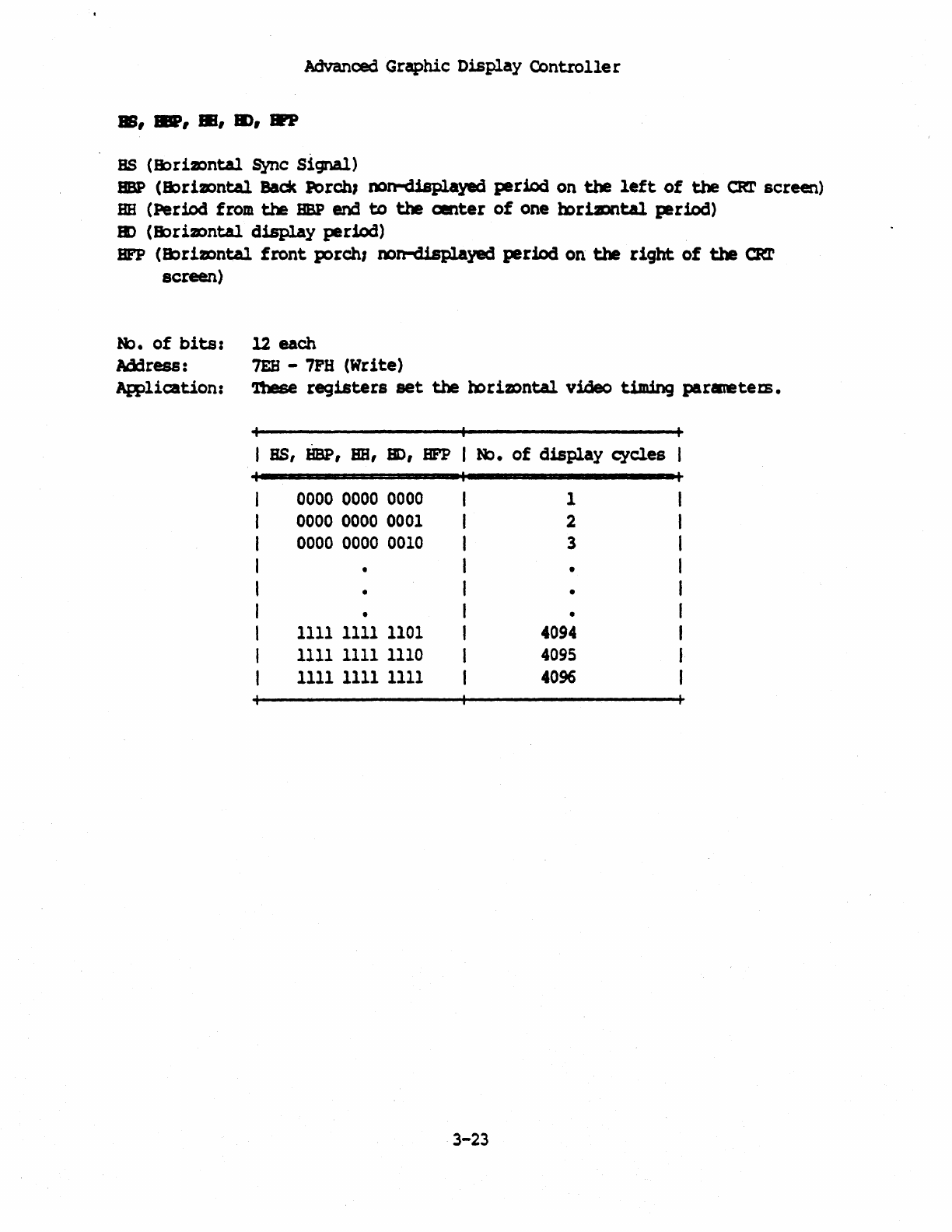
Advanced Graphic
Display
Control1e r
III,
&',
III,
Ill,
IPP
as
(Jl:)rimntal
Sync signal)
BBP
(Jt)ri2DntAl Back Porch, non-Qisplayed
period
on
the
left
of
the
CRT
screen)
BB
(Period from
the
BBP
end
to
the
center
of
one
mri2Dntal
period)
8)
(Jt)riJDntal
a1spl.ay
period)
BFP
(8:)rimntal
front
porchl non-displayec1
period
on
the
right
of
the
CRr
screen)
Ml.
of
bits:
12 each
Adlress:
7EB
-
7FH
(Write)
Application:
'l!lese
registers
set
the
blr
i20ntal
video
timing
parsrete
rs.
I
BS,
HBP,
BB,
11),
BFP
I Ml.
of
display
cycles
0000
0000
0000
1
0000
0000 0001
2
0000
0000
0010
3
• •
• •
• •
1111
1111 1101
4094
1111
1111
1110
4095
1111
1111
1111
4096
3-23
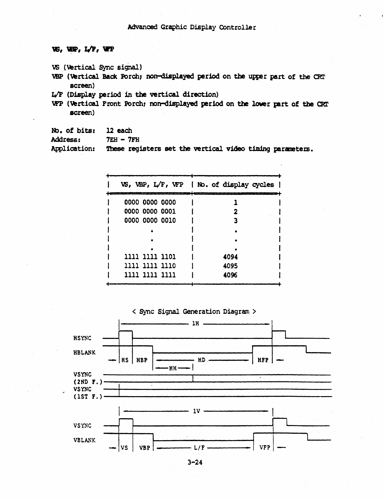
Advanced
Graphic Display Controller
.,
~,
LIP,
WP
VS
(Vertical
Sync
si;na.r)
VBP
(vartical
Back
Porch; non-displayec1
period
on
the
uR2r
part
of
the
CRI'
screen)
I/F
(Display
period
in
the
vertical
direction)
VFP
(vartical
Front Porch; oon-displayed period on
the
lower
plrt
of
the
em'
screen)
R>.
of
bits:
12
each
Address:
7EH
-
7FH
~ication:
'lhese
registers
set
the
vertical
video
timing
parauetem.
vs,
VBP,
WF,
VFP
I R>.
of
display
cycles
0000
0000
0000
1
0000
0000
0001
2
0000
0000
0010
3
• •
• •
• •
1111
1111
1101
4094
1111
1111
1110
4095
1111
1111 1111
4096
<
Sync
Signal
Generation
Diagram
>
HSYNC
L
1M
n
-
HBLANK
I
-
H5
HBP
HD,
HFP
-
-HH-I
VSYNC
(2ND
F.)
VSYNC
(151
F.)
I
1V
I
VSY'NC
1.i
I
vnE
VBLANK
VBpl
L/F
3-24
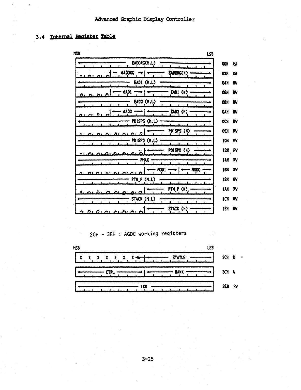
Advanced Graphic
Display
Controlle
r
3.4
Int;'mal
Register
!t'Iblt.
OON
IV
•
02H
IV
•
04"
IV
08H
IV
•
08H
tv
OAH
IV
OCH
IV
O£H
IV
IOH
IV
12H
IV
14H
R'J
ISH
IV
ISH
IV
lAM
IN
101
RV
1£H
R'J
20H
-
3BH
AGOe
working
registers
MSB
LS8
I X I X X X X X X
~
I'
SiATUS
-I
3CK
R 4
I
I '
em
. I •
BANK
·1
301
V
I I
I '
III
·1
3tH
RW
I
3-25
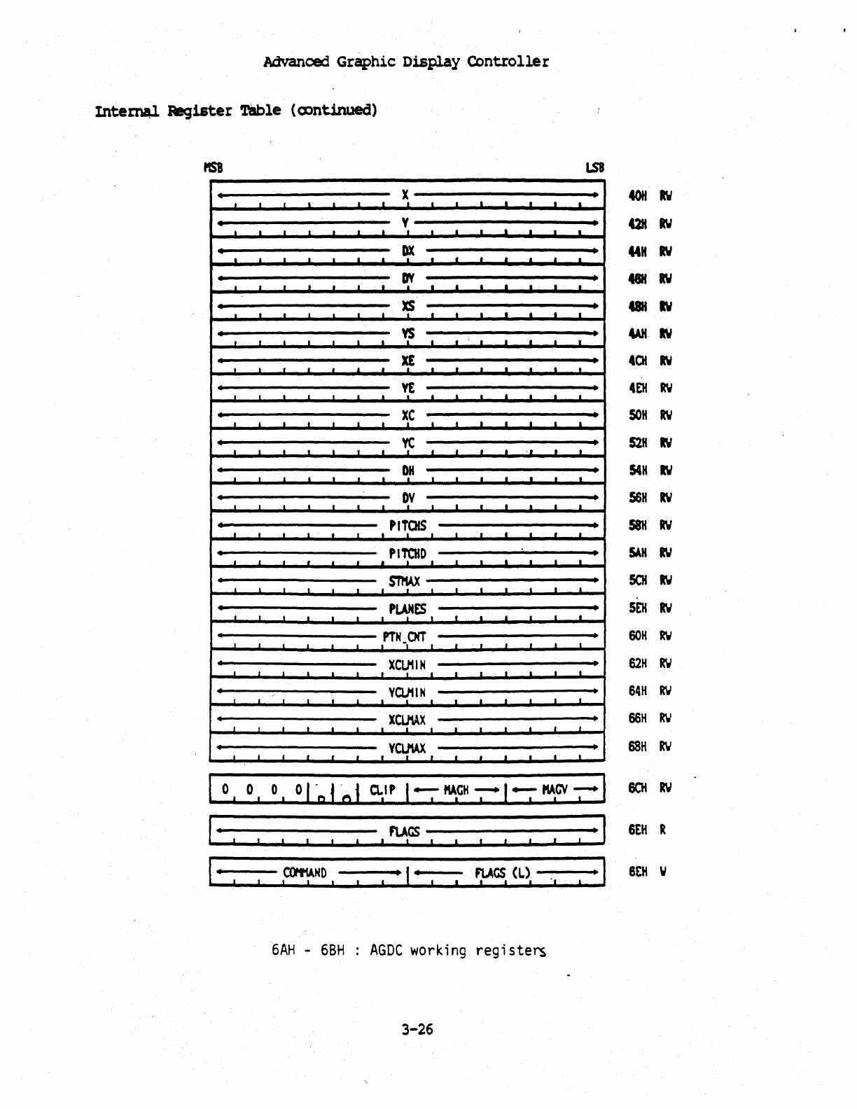
Advanced
Graphic
Display
Controlle
r
Inte~
Register
Table
(CX)ntinued)
LSI
• X •
40H
IV
I I I I I I · . I , • · • • •
• y •
• I I
~
· · · , · · • • • • ·
42H
IV
•
~
•
I I I ~ I I • • · · · , • I
44H
IV
•
~
•
I I • I ,
.-
I • • • • I 1 •
48H
RW
•
~
•
.1
I · , , , , • · · · • • •
48H
IV
•
~
•
, I
.1
1 , I I • • · · • I ·
4AH
IV
• ¥ •
.,
I
..
1 I I • • · · · · ...l I
401
IV
•
V!-
•
..1 1 · , • · · · · • • ,
4£H
IV
•
~C
•
..1 I .1
~
• I • • • • • • • 1
SOH
IV
•
~
•
• I • • · · · · I · · . , • •
52H
IV
•
~H
•
I I I • I · · · · · · • • I
54H
IV
•
~v
•
..1 1
.1
J I I I I I • • 1 • •
56H
IV
• •
PI~OIS
I •
I •
.~
• I , · I , •
58H
IV
• • PI1?D I •
· .
..
• · • I I I I I •
SAM
IV
•
I~
•
..1 I I I I I , · · I I I
5CH
IV
• I
P~ES.
•
I , I • · I • · · I I •
5£K
ltv
•
,PTN_,OO
• •
..1
I 1 I , , I I I J I
SOH
RW
• I
XCl!1IN
• •
...L
I I I , · I · · I I •
62H
ltv
• •
VCLt'IN
• •
.1 , , I • I I , I I
64H
R'W
•
XCU1AX
•
66H
RW
.1
, I I I I , • I I I I • I I
• •
vClt'AX
t •
.1
I I f • I · , · • I I
68H
R'e'
I
0 0 0 o
109
f
"Q
1
Q.IP
1--;-
~CH
~
1--;-
~cv
~
I
6CH
IV
I
I·
FLAGS
-I
6EH
R
1
I·
Cl)t1AND
. I ·
FLAGS
(L)
·1
6tH
v
I I I I I
'I
6AH
-
6BH
AGDC
working
registers
3-26
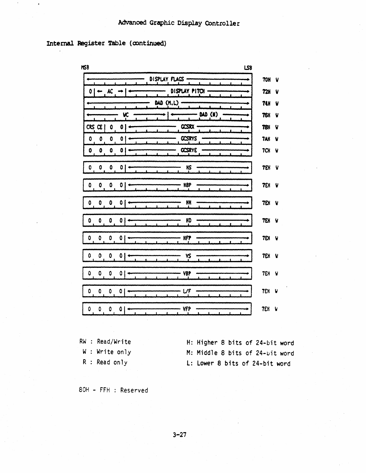
Advanced Graphic
Display
Controlle
r
Internal
Register
Table (Q)ntinued)
ttS8
lS8
• •
DI~LA~
~cs
.
I • t • I • I I •
•
10H
V
12M
V
01",.4(."'1-
• • I I i .
~
I
1
~
I I
c~
at
o t o I- I
o.
o~
0
01'
I
o t
O.
0.
01"
.
0 0 0 o I •
0 0 0 o I •
0 0 0 o I ·
0 0 0 o I •
0 0 0 o I ·
0 0 0 o I ·
0 0 0 o I ·
0 0 0 o I ·
0 0 0 o I ·
RW
Read/Wri
te
W
Write
only
R
Read
only
I
•
·
·
·
BOH
-
FFH
Reserved
I
DI~~
PI!?
I •
I , • ,
~
(,".1.).
• i • . I • •
1tH
"
1SH
"
1811
"
7AR
"
7CH
W
•
I
.
II I I I
,OAD
.(1) t •
I • ·
I
I
•
.
a:s.ax
, •
• I • •
I
a:srts.~
•
• , • I
-'
ccs.av£
, II
I • I I
HS
TEH
V
I
HSP
7EH
"
HH
7EH
"
HD
Hf?
7£11
W
,
VS
TEN
"
•
vap
7EM
\II
,
LlF
7EH
\t'
•
VFP
7EH
V
H:
Higher 8
bits
of
24-bit
word
M:
Middle
8
bits
of
24-uit
word
l:
Lower
8
bits
of 24-bit
word
3-27

Advanced
Graphic Display Controller
3-28
Advanced
Graphic Display
Controller
Section
4
4.1
Drawing
Functions
'!'be NZX:,
is
an
LSI
device
that
can perform
graphics
drawing
am
(X)pying
at
high
.
speed.
1!le
mst
system
specifies
the
drawing
plraneters
and
cxmnands
by
writing
to
specific
internal
AGlC
registem.
Q'lly
the
parsetem
that
are
needed
to
perform
the
drawing a:mnand
are
written.
When
the
DRAW
a:mnand
is
written,
the
~
starts
the
drawing
process.
'!bis
section
describes
the
variations
of
the
DRAW
a:mnand and
the
tBraneters
requi
red
fo
reach
oonmand.
The
DRAW
cx>nmand
is
set
in
the
cx:MMAID
register
at
address
6EH
-6FH. The
type
of
drawing
is
selected
according
to
the
op!ration
code
written
to
6FB.
~rious
ootrbinations
are
selected
by
the
flags
set
in
the
register
at
6EH.
The
DRAW
conmands
can roughly
be
classified
as
follows:
1.
Data
read
oormand
2.
Graphics drawing cxmnands
-Dot drawing
-
Straight
line
drawing
-
CUrve
drawing
3.
Paint
col'tllands
-N:>n-arbi
trary
area
paint
-
Arbitrary
area
paint
4.
Copy
conmands
-
Siuple
oopy
-
900
rotation
copy
-
Arbitrary
angle
rotation
oopy
-Enlarge/Shrink
cx>py
s.
PUT/GET
oonmands
-
PUT
-
GET
-
90
0
rotation
GET
4-1
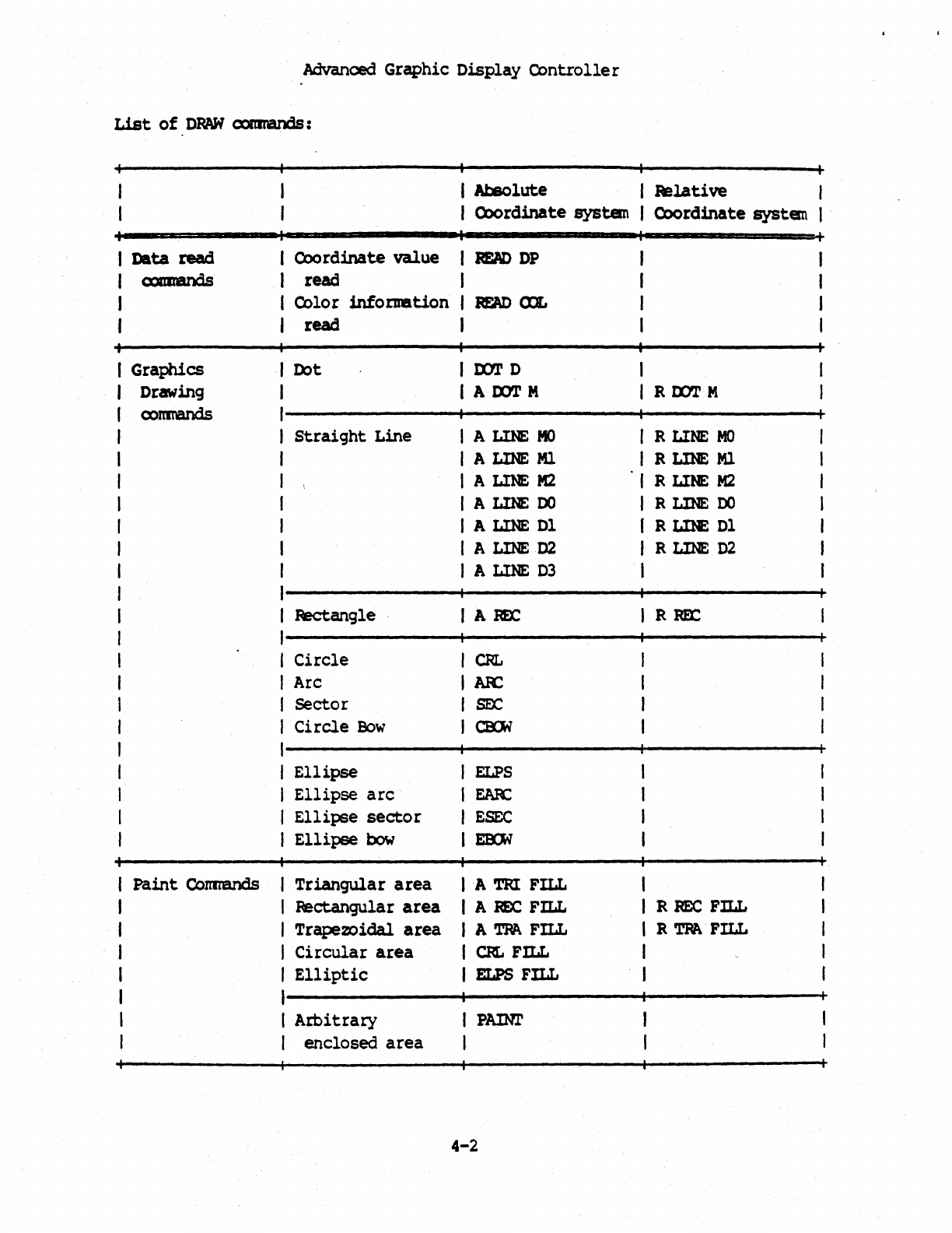
4-2
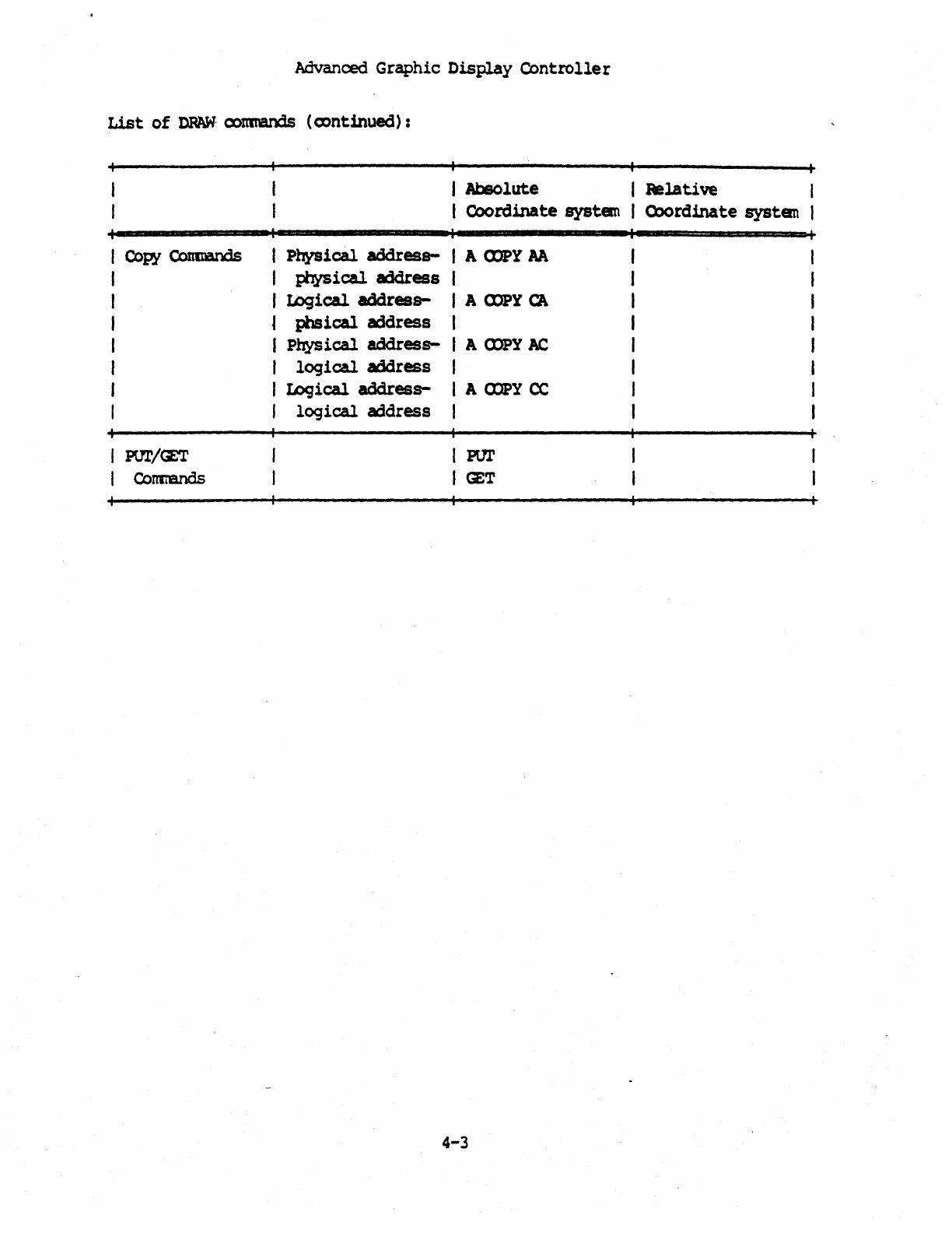
Advanced Graphic
Display
Controlle
r
List
of
DPAW·
oonm:mds ( ex>ntinued) :
I
Copy
Conmands
I
I
I
I
I
I
I
I Pm'/CET
I Cormands
I Absolute I
BelaU
ve I
I
Coordinate
systan
I Q)ord1nate
systan
I
I
Physical
address-
I A
CDPY
AA
I J;ttysical address I
I
IDgical
address- I A
CDPY
CA
I
phsical
address I
I
Physical
address-
I A
CDPY
AC
I
logical
address I
I
IDgical
address-
I A
CDPY
CC
I
logical
address I
I ror
I
GET
4-3
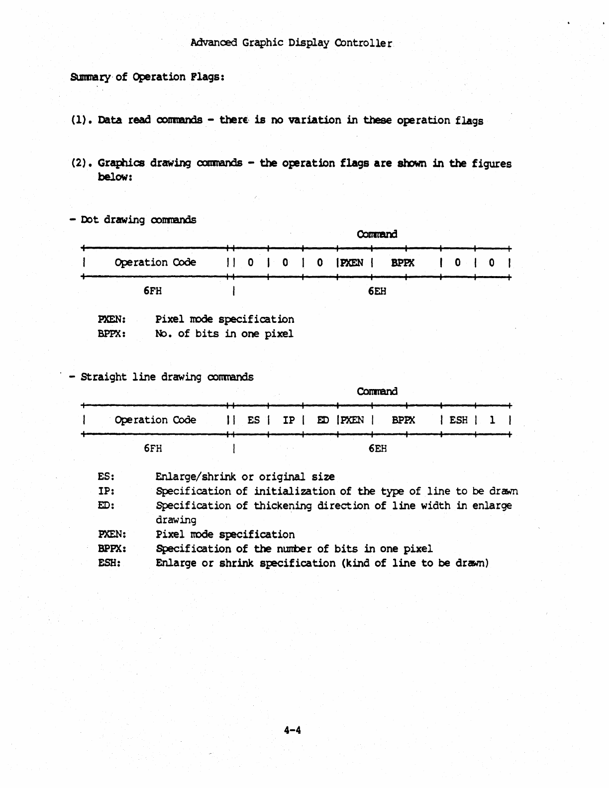
Advanced
Graphic Disp[ay
Controller
SUmmary'of
Operation
Flags:
(1).
Data
read
coummds
-ther£·
is
no
variation
in
these
operation
flags
(2).
Graphics drawing cxmnands -
the
operation
flags
are
sl'¥7tm
in
the
figures
below:
-
~t
drawing
ooImBnCis
II
Operation
Code
II
0 o o I
PXEN
I
8PPJC
o o
II
6FH
6EH
PXEN:
Pixel
node
specification
BPPX:
NJ.
of
bits
in
one
pixel
-
Straight
line
drawing
oomnands
II
Ope
ration
Code
II
ES
IP
ED
I
PXEN
I
BPPA
ESH
1
I I
6FH
6EH
ES:
Enlarge/shrink
or
original
size
IP:
Specification
of
initialization
of
the
type
of
line
to
be
drawn
ED:
Specification
of
thickening
direction
of
line
width
in
enlarge
drawing
PXEN:
Pixel
node
speCification
BPPX:
Specification
of
the
nUJtber
of
bits
in
one
pixel
ESH:
Enlarge
or
shrink
specification
(kind
of
line
to
be drawn)
4-4
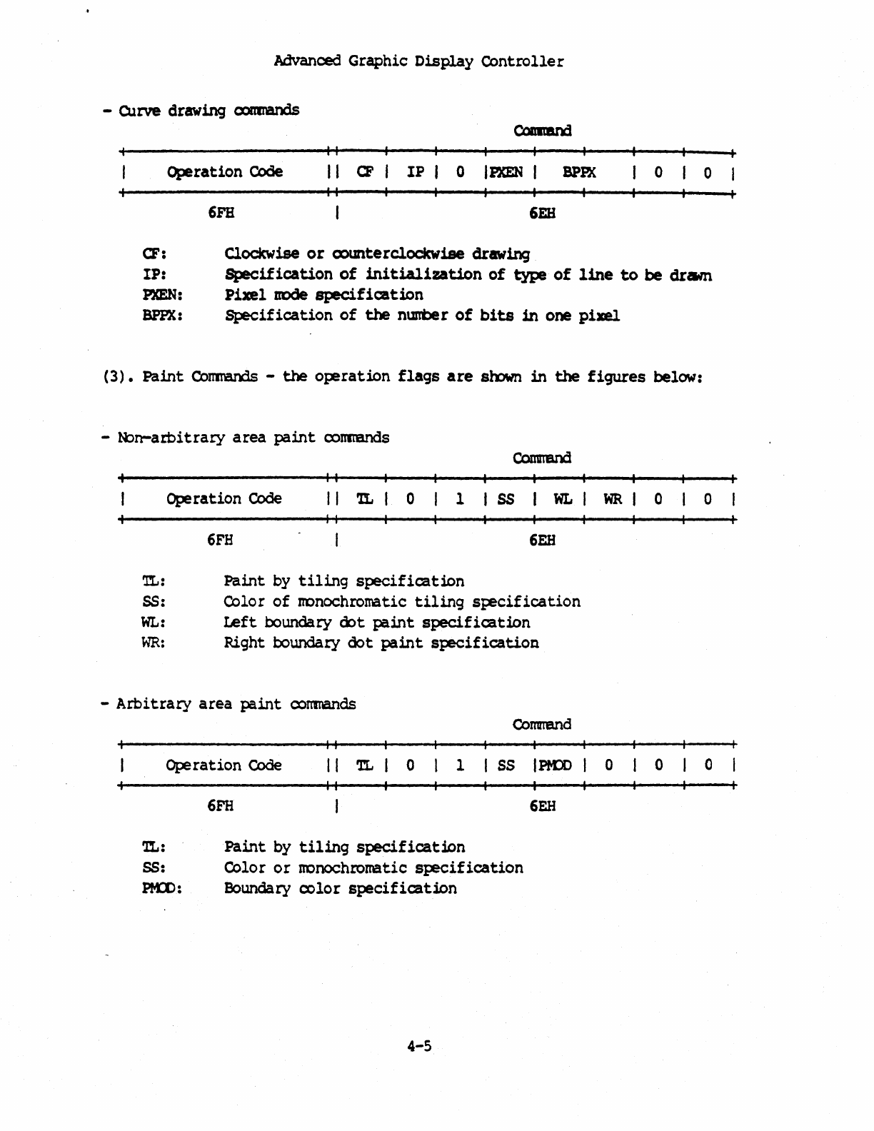
Advanced
Graphic
Display
Contrelle
r
-CUrve
drawing
cxmmands
II
Operat:ion Code
II
CF
IP
o I
FJCEN
I
SPPA
o o
II
6FB
6E1i
G':
Clockwise
or
Q')unterclockwise
drawing
IP:
Specification
of
initialization
of
type
of
line
to
be
dram
PXEN:
Pixel
node
specification
BPPX:
Specification
of
the
nunb! r
of
bits
in
one
pixel
(3).
Paint:
ColIltiUXls
-
the
oparation
flags
are
srown
in
the
figures
below:
-
~n-aIbitrary
area
paint
ooImBnds
II
Operation
Code
II
'XL
o 1
SSIWLIWR
o o
It
6FH
6EH
'lL:
Paint
by
tiling
specification
ss:
Color
of
nonochromatic
tiling
s{:ecification
WL:
IA!ft
boundary
tbt
paint
specificat:ion
WR:
Right
boundary
dot
paint
st:eCification
-
Arbitrary
area
paint
oonmands
Comrrend
t I
Operation
Code
II
'l'L o 1 S5
IPIDD
I 0 o o
II
6FH
6EH
'IL:
Paint
by
tiling
specificat:ion
ss:
Color
or
nonochromatic
specification
PM:D:
Boundary
oolor
specification
4-5
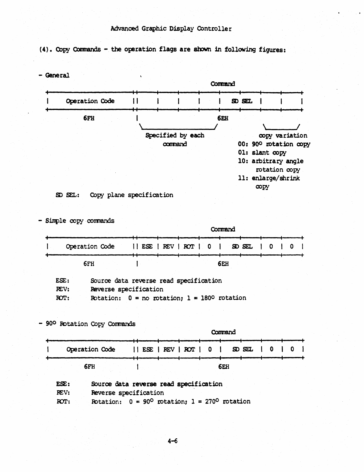
Advanced Graphic
Display
Controlle
r
(4).
CoFi
CCmnands
-
the
operation
flags
are
sbJwn
in
following
figures:
-
General
Operation
Code
6Fa
, I
II
II
I
6EH
,
_________________
1
Specified
by
each
cxmnand
S)
SEL:
Copy
plane
specification
-Sirtple oopy·
ex>rmands
a:>p.{ va
ration
00:
9oo
mtation
CDp.{
01:
slant
cx>py
10:
arbitrary
angle
rotation
ooF.{
11:
enlarge/shrink
oopy
Comrrand
II
Operation
Code
I I
ESE
I
REV
I
KY.I'
o o o
II
6FH
6EH
ESE:
Source
data
reve
rse
read
specif
ication
H:V:
Reverse
specification
lOT: R>tation: 0 = no
lOtation7
1 = 1800
rotation
-
90
0 R:>tation Copy
Conrcands
II
Operation
Code
I I
ESE
I
REV
I
R)T
o
S)
SEL
o o
II
6FH
6EH
ESE:
Source
data
reverse
read
s~fication
~V:
Pieverse
specification
lOT:
R>tation:
0 =
90
0 lOtation7 1 = 2700
rotation
4-6
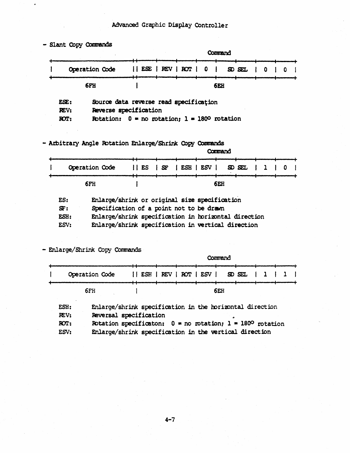
Advanced
Graphic
Display
Controller
-
Slant
Copy
Camands
II
Operation
Code
IIESEIm:vIImIO
I r
6PH
6EH
ESE:
Q)urce
data
reverse read
specification
EV:
Reverse
specification
101':
Rltation:
o·
no
mtation;
1 • 1800
rotation
-
Atbitrary
Angle
ltltation
Enlarge/Shrink
Copy
Coummds
camand
II
Operation
Code
J I ES
SF
I
ESH
I
ESV
I
SO
BEL
II
6FH
6EH
ES:
Enlarge/shrink
or
original
size
specification
SF:
Specification
of
a
point
not
to
be
drawn
o
1
ESE:
Enlarge/shrink
specification
in
mri2Dntal
direction
ESV:
Enlarge/shrink
specification
in
vertical
direction
-
Enlarge/Shrink
Copy
Conmands
Operation
Code
6FH
II
I I
ESH
I
REV
I :Ear I
ESV
I
S)
BEL
II
6EH
1
ESE:
Enlarge/shrink
specification
in
the
mri2Dntal
direction
~V:
Reversal
specification
,.
o
o
1
tar:
lCtation
specific:aton:
0 = no
rotation;
1 • 1800
rotation
ESV:
Enlarge/shrink
specification
in
the
vertical
direction
4-7
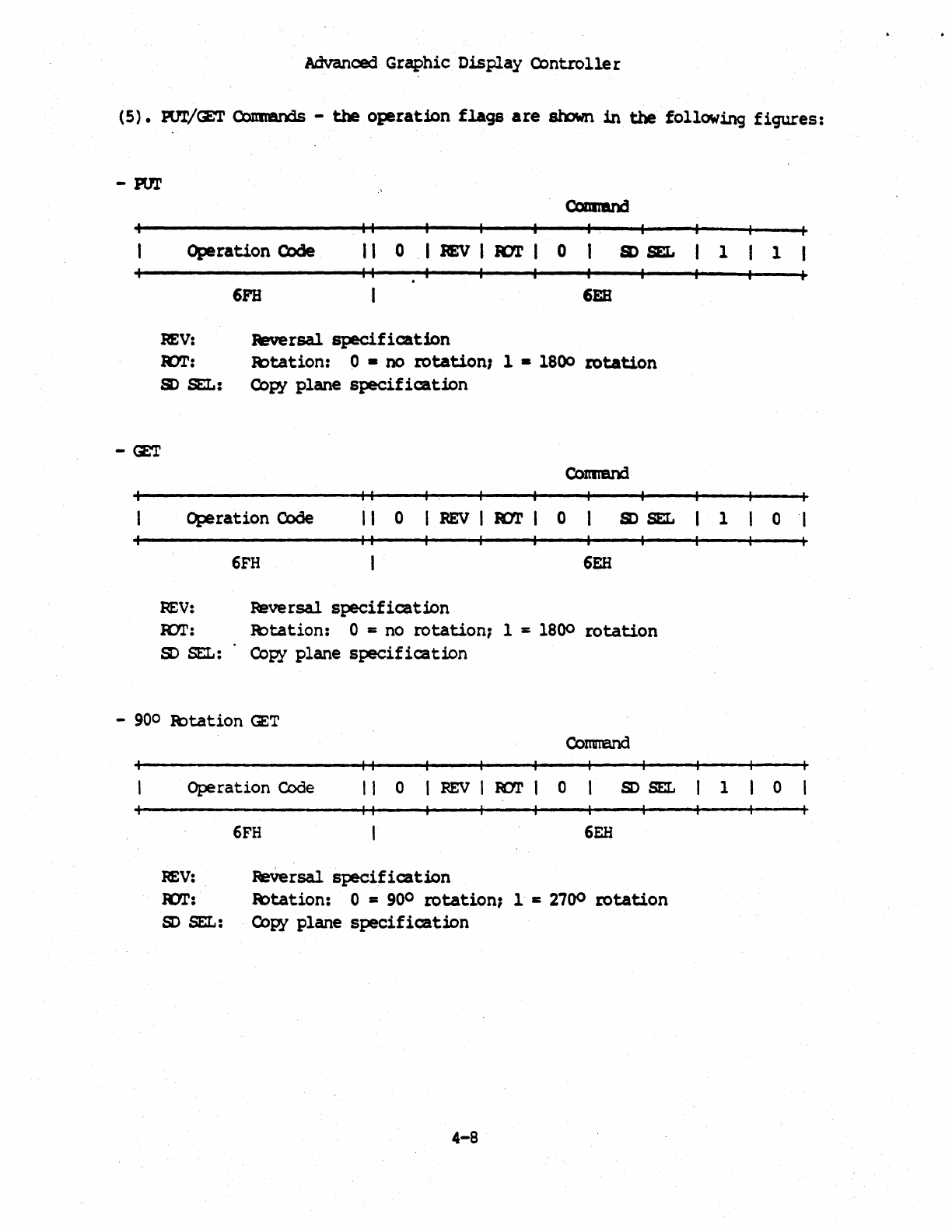
Advanced·
Graphic
Display
Controlle
r
(5).
PUl'/CET
COImBnds
-
the
operation
flags
are
smwn
in
the
follOWing
figures:
-Pm'
II
I .
Operation
Code
110
I
REV
I
R7l'1
0 S>
BEL
1 1
II
6PH
6£8
REV:
Reversal
specification
R:1I':
a.">tation:
o·
no
rotation;
1 • 1800
rotation
S>
BEL:
Q)py
plane
specification
-
CET
II
I .
Operation
Code
110
IREVIR7.l'1 0 1
II
6FH
6EH
EV:
Reversal
specification
R7I': a.">tation: 0 = no
rotation
1 1
=:
1800
rotation
s:>
SEL:
Copy
plane
specification
-900 R::>tation
GET
Comrrand
II
Operation
Code
IIOIREVIKYl'
o 1 o
I I
6FH
6EH
REV:
~versal
specification
R:1.I':
it>tation:
0 =
90
0
rotationl
1
II:
27()o
rotation
SO
SE:L:
Copy
plane
specification
4-8
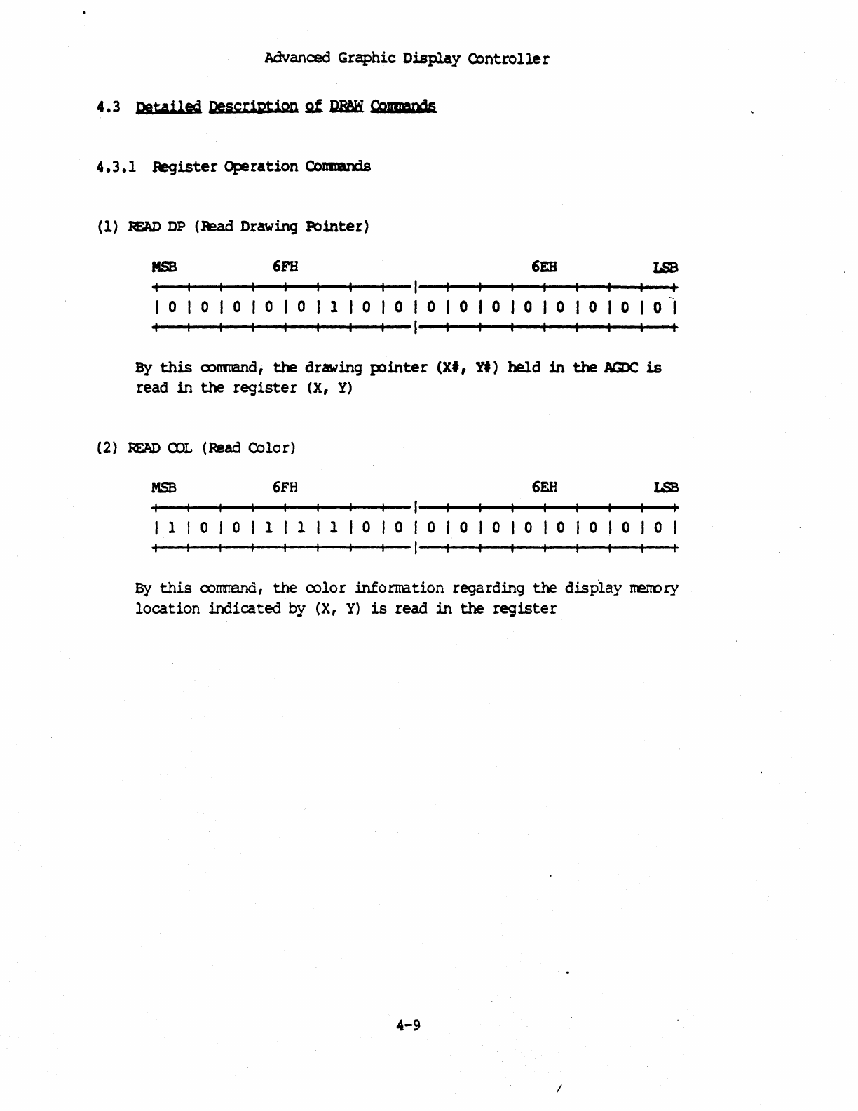
Advanced
Graphic
Display
Controller
4.3
Detailed
Description
gf
Im6Ii
CPJmMds
4.3.1
aegister
Operation Coummds
(1)
~
DP
(lead
Drawing
Pointer)
MSB
6FB
6EB
LSB
.1
I--~~--~-+--~-+--+--+
00000110101010101010101010··,
+--+--+--+--~-+--~~--I--~~--~~--~~~~~
By
this
oorme.nd,
the
drawing
pointer
(XI,
YI)
held
in
the
NDC
is
read
in
the
register
(X,
Y)
(2)
~
CDL (Read Color)
MSB
6FH
6EH
LSB
100
1 1 1 I 0
100
0 0 0 I 0 I 0 0 0
By
this
cormand,
the
color
information
regarding
the
display
nenory
location
indicated
by
(X,
Y)
is
read
in
the
register
4-9
I
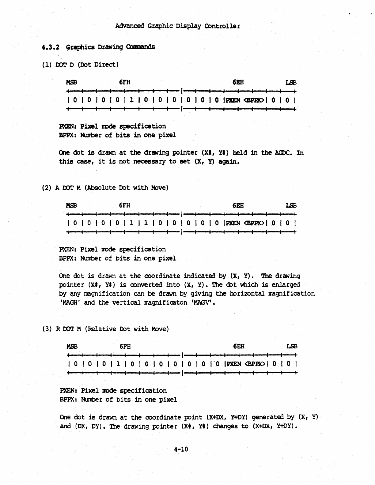
Advanced
Graphic
Display
Controlle
r
4.3.2
(1)
IX1I'
D (Ik>t
Direct)
MSB
6FH
6EH
LSB
o 0 0 0 1 0 0 0 0 I 0 I 0
IP.KEN
<BPP.K>I
0 I 0 I
PXE:N:
Pixel
!rOde
specification
BPPX:
ttmber
of
"bits
in
one
pixel
Ckle
d::>t
is
drawn
at
the
drawing
pointer
(xt,
yt)
held
in
the
ACDC.
In
this
case,
it
is
not
necessary
to
set
(X, Y)
again.
(2)
A ror M
(Absolute
D:>t
with
f.k:>ve)
MSB
6FH
6EH
LSB
o 0 0 0 1 1 0 0 0 0 0
IPXEN
<BPPDIO 0
PXEN:
Pixel
node
specification
BPPX:
NJrrber
of
bits
in
one
pixel
One
oot
is
drawn
at
the
ex>ordinate
indicated
by
(X,
Y).
The
drawing
IX>inter (XI, YI)
is
oonverted
:into (X,
Y).
'!he
d:>t
which
is
enlarged
by
any
nagnification
can
be
drawn by
giving
the
lx>rizontal
magnification
'MAGH
t and
the
vertical
magnificaton
'MAGV'.
(3) R
IXY!'
M
(Relative
Ibt
with
ftbve)
MSB
6FH
6EH
LSB
o 0 0 1 0 0 0 0 0 0
"0
IP.XEN
<BPP.K>I
0 I 0
PXEN:
Pixel
node
specification
BPPX:
Nurrt>er
of
bits
in
one
pixel
I .
<Ale
oot
is
drawn
at
the
cxx>rdinate p:>int
(X+DX,
Y+DY)
generate:1
by
(X,
Y)
and
(DX,
DY).
The
drawing
pointer
(XI,
YI) changes
to
(X-tDX,
Y+DY).
4-10
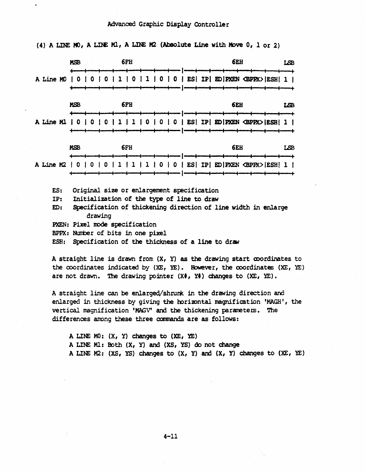
Advanced
Graphic
Display
Controlle
r
(4)
A LINE
1«),
A
LItE
Ml, A LINE
M2
(Absolute Line
with
It>ve
0,
1
or
2)
MSB
6FH
6EH
LSB
I f
A
Line
MO
0 0 0 1 0 1 0 0 I
ESI
IPI
EDIPXEN
<BPPJC>
IEBBr
1 I
I
MSB
6FB
6EB
LSB
I
A
Line
Ml
0 0 0 1 1 0 0 0 I Est
IPI
EDIPXEN
<BPro
IE881
1 I
I
MSB
6FH
6EH
LSB
I
A
Line
M2
0 0 0 1 I 1 I 1 0 0 I
ESI
IPI
EDIPXEN
<BPP.A>IESHI
1 I
I
ES:
Original
size
or
enlargerrent
specification
IP:
Initialization
of
the
type
of
line
to
draw
ED:
Specification
of
thickening
direction
of
line
width
in
enlarge
drawing
PXEN:
Pixel
node
specification
BPPX:
Nurtber
of,
bits
in
one
pixel
ESH:
Specification
of
the
thickness
of
a
line
to
draw
A
straight
line
is
drawn from (X,
Y)
as
the
drawing
start
(X)()rdinates
to
the
ooordinates
indicated
by
(XE, YE).
However,
the
coordinates
(XE,
l:E)
are
not
drawn.
The
drawing
pointer
(XI,
YI) changes
to
(XE, YE).
A
straight
line
can
be
enlarged/shrunk
in
the
drawing
direction
and
enlarged
in
thickness
by
giving
the
b:>ri2Dntal
magnification
'MAGH
I,
the
vertical
magnification
'MAGV'
and
the
thickening
paraneters.
The
differences
anong
these
three
carrnands
are
as
follows:
A
LINE
MO:
(X,
Y)
changes
to
(XE,
YE)
A
LINE
Ml: Both (X,
Y)
and
(XS,
YS)
do
not
change
A
LINE
M2:
(XS,
YS)
changes
to
(X,
Y)
arx1
(X,
Y)
changes
to
(XE,
~)
4-11
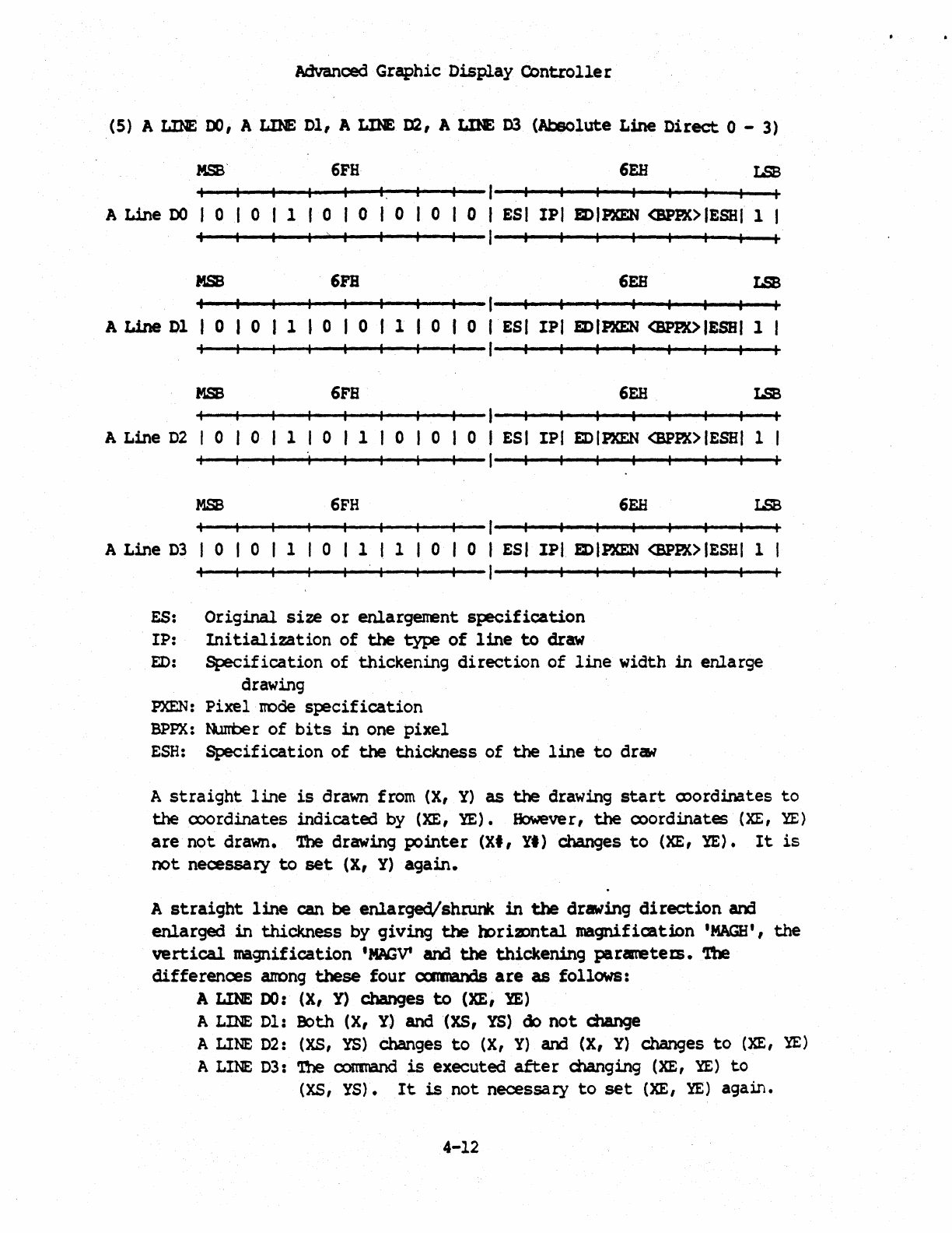
Advanced
Graphic
Display
Controlle
r
(5) A
LINE
DO,
A
LINE
D1, A
LINE
D2, A
LIE
D3
(Absolute
Line
Direct
0 - 3)
6FH
6EH
LSB
+-~--~~--~--~~--+--I--~~--~~--~~~~~
A Line
DO
0 0 1 I 0 I 0 0 0 0 I ESI
IPI
EDIPXEN
<&PEt>
IEBBI
1 I
I ) I I
MSB
6PH
6EH
LSB
+-~--~~--~--~~--+--I--~~~~--~~--+--+--~
A
Line
D1
0 0 1 I 0 I 0 1 0 0 I ESI
IPI
mlPXEN
<BPPX>IESBI
1 I
I
MSB
6FB
6EH
LSB
+-~--~~--~--~~--+--I--~~--~~--~~~~~
A
Line
D2
0 0 1 0 1 0 0 0 I ESI
IPI
EDIPXEN
<BPPA>
IEBBI 1 I
I
MSB
6FH
6EH
+-~--~~--~--~~--+--I--~~--~--~~--+--+--*
A
Line
D3
0 0 1 0 1 1 0 0 I ESI
IPI
EDIPXEN
<BPPA>
IESBI 1 I
I I
ES:
Original
size
or
enlargenent
specification
IP:
Initialization
of
the
type
of
line
to
draw
ED:
Specification
of
thickening
direction
of
line
width
in
enlarge
drawing
PXEN:
Pixel
node
specification
BPPX:
N-uri:>er
of
bits
in
one
pixel
ESH:
Specification
of
the
thickness
of
the
line
to
draw
A
straight
line
is
drawn from (X,
Y)
as
the
drawing
start
(l)ordinates
to
the
ooordinates
indicated
by (XE,
IE).
However,
the
coordinates
(XE,
~)
are
not
drawn.
The
drawing
pointer
(xt,
yt)
changes
to
(XE,
YE).
It
is
not
necessary
to
set
(X,
Y)
again.
A
straight
line
am
be
enlarqed/shnmk
in
the
drawing
direction
an.]
enlarged
in
thickness
by
giving
the
mriz:mtal
magnification
'MAGS',
the
vertical.
magnification
'MAGV'
aoo
the
thickening
parsneter:s.
The
differenoes
anong these
four
oarmands
are
as
follows:
A
LINE
DO:
(X,
Y)
changes
to
(XE,
IE)
A LINE D1:
Both
(X,
y,)
and(XS,
YS)
00
not
dlanqe
A
LINE
D2: (XS,
YS)
changes
to
(X,
Y)
and (X,
Y)
changes
to
(XE,
l'E)
A
LINE
D3: '!be
CX>ItIlIandis
executed
after
dlanging
(XE,
IE)
to
(XS,
YS).
It
is
not
necessary
to
set
(XE,
YE)
again.
4-12
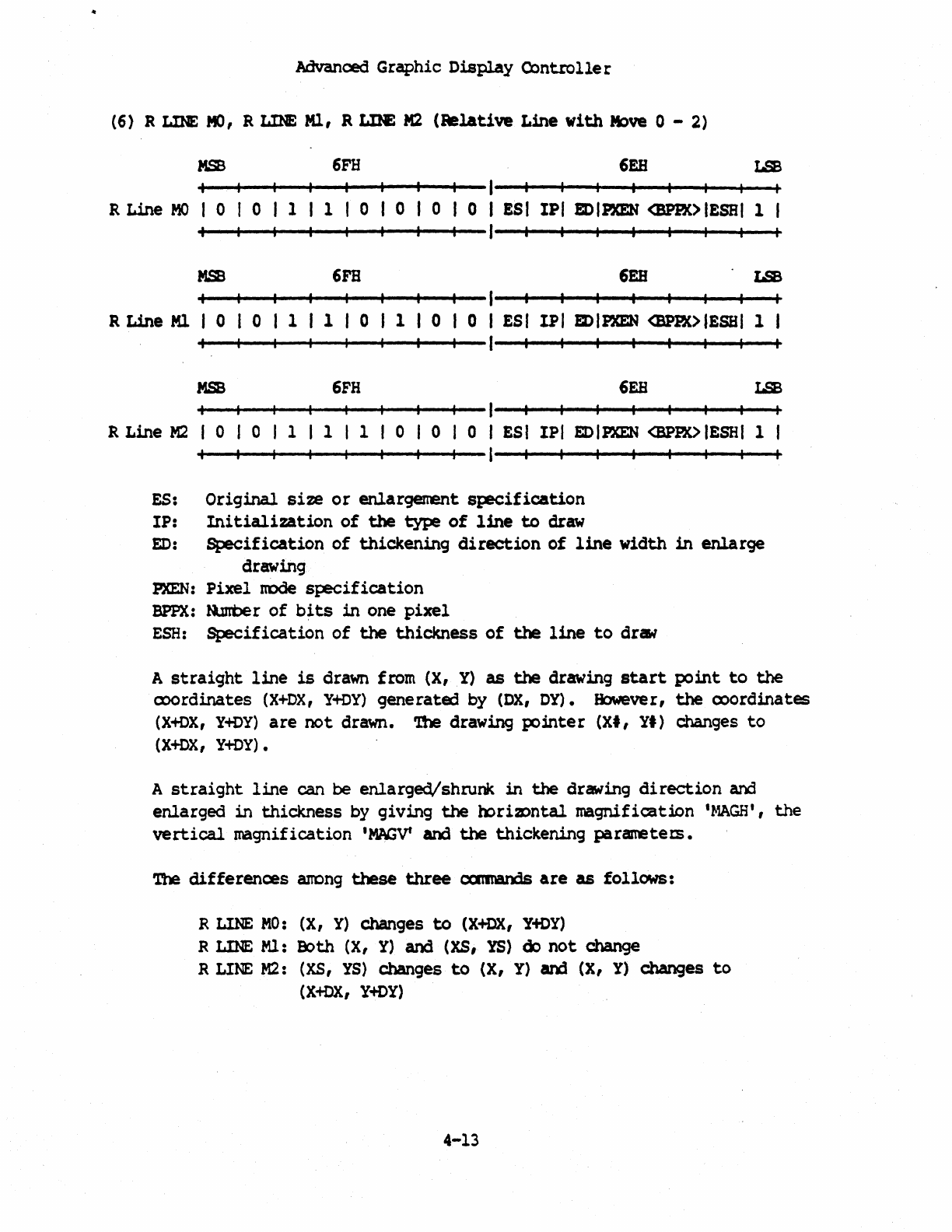
Advanced
Graphic
Display
Controlle
r
(6)
R
LINE
11),
R
LINE
Ml,
R
Ln£
M2
(Relative
Line
with
)t)ve 0 -
2)
MSB
6FH
6EH
LSB
I
R
Line
MO
0 0 1 1 0 0 0 0 I
ESI
IPI
EDIPJCEN
<BPBt>
IESHI
1 I
I
MSB
6FB
6EB
LSB
I
R
Line
Ml
0 0 1 1 0 1 0 0 I
ESI
IPI
mlPXEN
<BPPA>IESBI
1 J
I
MSB
6FH
6EB
LSB
I
R
Line
M2
0 0 1 1 1 0 0 0 I
ESI
IPI
EDIPXEN
<BPPA>
IESHI
1 I
I
ES:
Original
size
or
enlargement
specification
IP:
Initialization
of
the
type
of
line
to
draw
ED:
Specification
of
thickening
direction
of
line
width
in
enlarge
drawing
PXEN:
Pixel
node
specification
BPPX:
9.JJrber
of
bits
in
one
pixel
ESH:
Specification
of
the
thickness
of
the
line
to
draw
A
straight
line
is
drawn from
(X,Y)
as
the
drawing
start
PJint
to
the
cx>ordinates
(X+DX,
Y+DY)
9enerate:!
by
(OX,
DY).
However,
the
(X)ordinates
(X+DX,
Y+DY)
are
not
drawn. '!be drawing p:>inter
(XI,
YI) changes
to
(X+DX,
Y+DY).
A
straight
line
can be
enlarged/shrunk
in
the
drawing
direction
and
enlarged
in
thickness
by
giving
the
oorimntal
magnification
'l-1AGH',
the
vertical
magnification
'MAGV'
and
the
thickening
paraneteIS.
The
differences
anong
these
three
cxmnands
are
as
follows:
R
LINE
MO:
(X,
Y)
changes
to
(X+DX,
Y+DY)
R
LINE
Ml:
Both (X,
Y)
and
(XS,
YS)
Q:)
not
change
R
LINE
M2:
(XS,
YS)
changes
to
(X,
Y)
arx1
(X,
Y)
changes
to
(X+OX,
Y+DY)
4-13
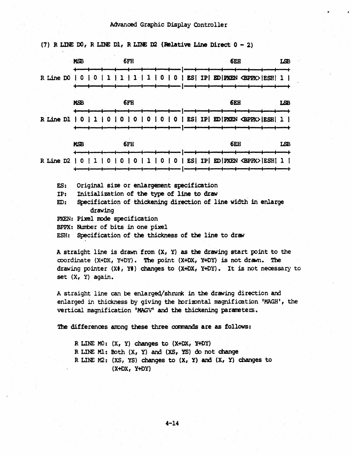
Advanced Graphic
Display
Controlle
r
(7) R
LINE
DO,
R
LINE
D1,
R
Ln£
D2
(Relative
Line
Direct
0 - 2)
MSB
6FH
6EH
LSB
+-~--~~--~--~~--+--I--~~--~--~~--+--+--~
R
Line
DO
0 0 1 1 1 1 0 0 I
ESf
IPI
£[)IPX£N
<B:PPA>
IESSI
1 I
I
MSB
6FB
6EH
LSB
+-~--~~~~--~~--+--I--~~--~--~-P--~-+--+
R
Line
D1
0 1 0 I 0 I 0 I 0 0 0 I
ESI
IPI
EDIPXEN
<aPE{>
IESBI
1 I
I
MSB
6FH
6EH
LSB
+-~--~~--~--~-'--+--I--~~--~--~-P--+--+--*
R
Line
D2
0 1 0 0 0 1 0 0 I
ESI
IPI
EDIPXEN<BPPA>IESHI
1 I
I
ES:
Original
size
or
enlargement
specification
IP:
Initialization
of
the
type
of
line
to
draw
ED:
Specification
of
thickening
direction
of
line
width
in
enlarge
drawing
PXEN:
Pixel
JrDde
specif
ica
tion
BPPX:
tlmbe
r
of
bits
in
one
pixel
ESH:
Specification
of
the
thickness
of
the
line
to
draw
A
straight
line
is
drawn from (X,
Y)
as
the
drawing
start
p:>int
to
the
a:>ordinate
(X+DX,
Y+DY).
The
point
(X+OX,
Y-tDY)
is
not
dram.
The
drawing p:>inter (XI, YI) changes
to
(X-t{)X,
Y+DY).
It
is
not
necssary
to
set
(X,
Y)
again.
A
straight
line
can be
enlarged/shrurit
in
the
drawing
direction
and
enlarged
in
thickness
by
giving
the
oori20ntal
magnification
'MAGE',
the
vertical
magnification
'MAGV'
and
the
thickening
parartetets.
'!be
differences
anong
these
three
cx:mnands
are
as
follows:
R
LINE
MO:
(X,
Y)
changes
to
(X+DX,
y-tDY)
R
LINE
Ml: Both (X,
Y)
and
(XS,
YS)
00
not
change
R
LINE
M2:
(XS,
YS)
changes
to
(X,
Y)
and
(X,
Y)
changes
to
(X+DX,
Y-tDY)
4-14
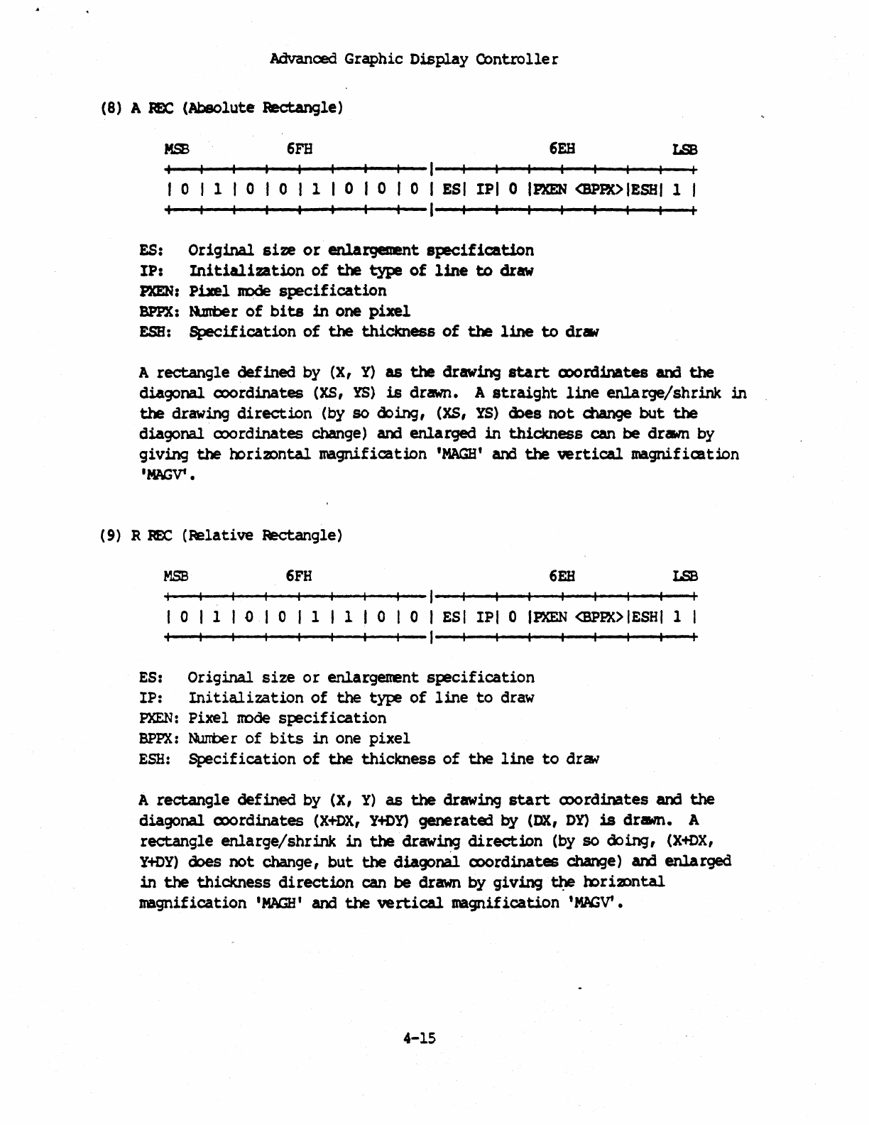
Advanced
Graphic
Display
Controlle
r
(8) A
~
(Absolute
Rectangle)
MSB
6FH
6EB
LSB
+--+--~~--~~~~--~-I--~~~~--~~--+--+--~
o 1 0 0 1 0 0 0 I ESI IPI 0
IPXEN
<BPPDIESHI 1 I
+--+--~~--~~~~--~-I--~~~~--~-P--+--+--~
ES:
Original
size
or
enlargement
specification
IP:
Initialization
of
the
type
of
line
to
araw
PXEN:
Pixel
JIDde
specification
BPPX:
Rmber
of
bits
in
one
pixel
EBB:
Specification
of
the
thickness
of
the
line
to
drat
A
rectangle
defined
by
(X,
Y)
as
the
drawing
start
Q)Ordinates
and
the
diagonal
c:xx>rdinates (XS,
YS)
is
drawn. A
straight
line
enlarge/shrink
in
the
drawing
direction
(by
so
doing,
(XS,
YS)
mes
not
d1anqe
but
the
diagonal
(X)()rdinates change) and
enlarged
in
thickness
can
be
drawn
by
giving
the
oori20ntal
magnification
'MAGS'
and
the
vertical
magnification
'MAGvt
•
(9)
R:ROC
(Ielative
Rectangle)
6FH
6EH
+-~--~~--~--~~--+--I--~~~~--~~--+-~--~
o 1 I
~
I
OIl
0 0 I
ESI
IPI 0
IP.XEN
<BPP.K>IESHI
1
+--+--~~--~--~~--+--I--~~~~--~~--+-~--~
ES:
Original
size
or
enlargement
specification
IP:
Initialization
of
the
type
of
line
to
draw
PXEN:
Pixel
node
specification
BPPX:
N.mt>er
of
bits
in
one
pixel
ESH:
Specification
of
the
thickness
of
the
line
to
draw
A
rectangle
defined
by
(X,
Y)
as
the
drawing
start
Q)()rdinates and
the
diagonal
CX)()rdinates
(X+DX,
Y+Dy)
generated
by
(OX,
Dy)
is
drawn. A
rectangle
enlarge/shrink
in
the
drawing
direction
(by
so
doing,
(X-tDX,
Y+DY)
does
not
change,
but
the
diagonal
ax>rdinates
change)
am
enlarged
in
the
thickness
direction
can
be
drawn
by
giving
~
mri2Dntal
magnification
'MAGS'
and
the
vertical
magnification
'MGV'.
4-15
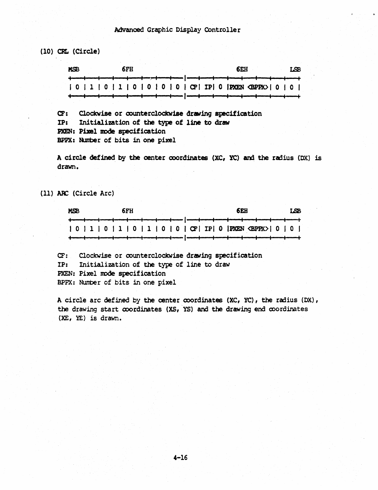
Advanced
Graphic
Dis~y
Controller
(10)
em.
(Circle)
MSB
6FB
6EH
LSB
+-~--~~--~--~I-_.~t~I--+--I--~~--~--~~--+--+--~
o 1 0 1 0 0 0 0 I
CPI
IPI
0
IPIEN
<BPPK>I
0 I 0 I
+-~--~~~~--~-+--+--I--~~--~~--~~~~-*
CF: Clockwise
or
counterclockwise
dr_ing
specification
IP:
Initialization
of
the
type
of
line
to
draw
PXEN:
Pixel
IIDde
specification
BPPX:
R.mber
of
bits
in
one
pixel
A
circle
defined
by
the
center
(X)()rdinates (XC,
te)
am
the
radius
(OX)
is
drawn.
(11)
~
(Circle
Arc)
MSB
6FH
6EB
LSB
+-~--~~--~--~-+--+--I--~~--~--~~--+--+--~
o 1 0 1 0 1 0 0 I
eFl
IPI 0
IP.XEN
<BPPK>I
0 0
+--+--~~--~--~~--+--l--~~--~--~~--+--+--~
CF: Clockwise
or
oounterclockwise drawing
specification
IP:
Initialization
of
the
type
of
line
to
draw
PXEN:
Pixel
node
specif
ication
BPPX:
Nunt>er
of
bits
in
one
pixel
A
circle
arc
defined
by
the
center
cx>ordinates (XC, YC),
the
radius
(DX),
the
drawing
start
Q)()rdinates (XS,
'ys)
and
the
drawing end cx>ordinates
(XE,
YE)
is
drawn.
4-16
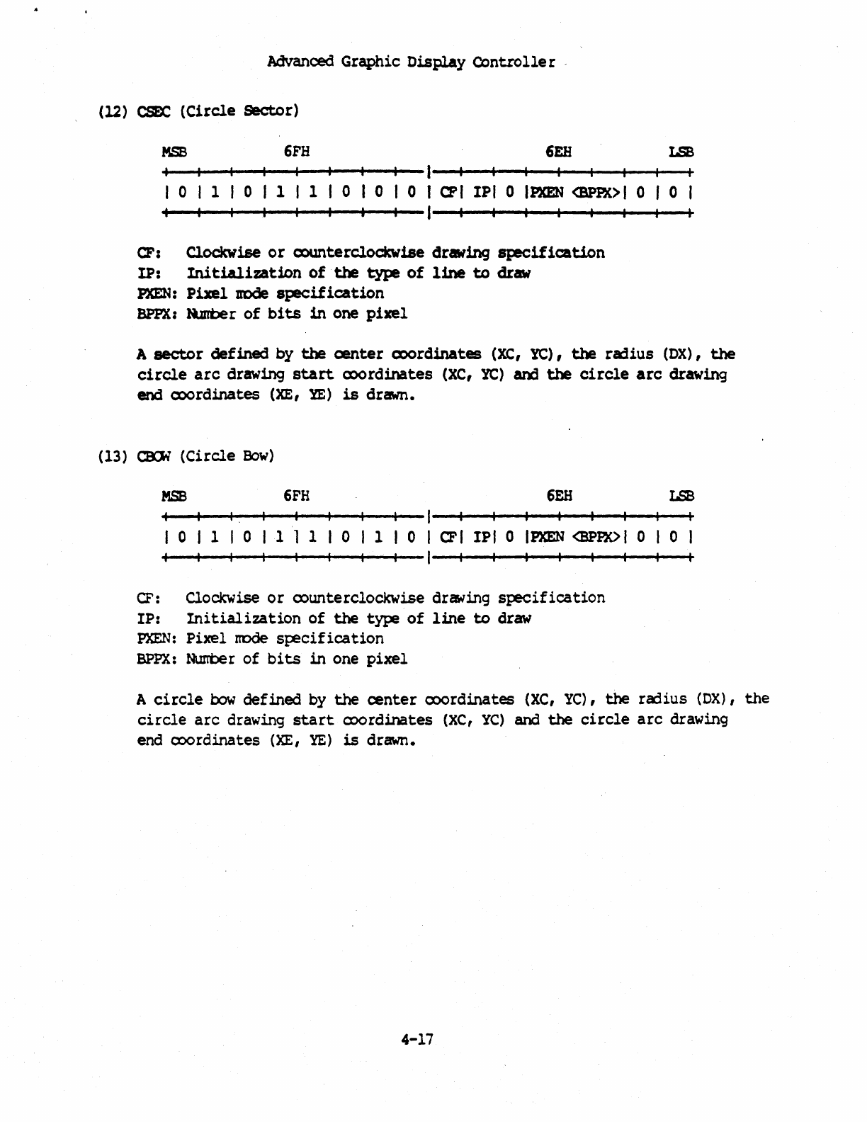
Advanced
Graphic
Display
Controlle
r '
(12)
CE
(Circle
Sector)
MSB
6FH
6EH
LSB
+--+--~~--~~~~--p--I--~~~~--~-P--+--+--~
o 1 0 1 1 0 I 0 I 0 I
CPI
IPI 0
IP.X!N
<BPP.K>I
0 0
+-~--~~--~--~-r--+--I--~~--*-~--~~--~~
CF:
Clockwise
or
c::ounterclockwise drawing
spK:ification
IP:
Initialization
of
the
type
of
line
to
draw
PXEN:
Pixel
JrOde
specification
BPPX:
IUrber
of
bits
in
one
pixel
A
sector
defined
by
the
center
Q)()rdinAtes
(XC,
YC),
the
raiius
(DX),
the
circle
arc
drawing
start
cx>ordinates
(XC,
YC)
and
the
circle
arc
drawing
end cx>ordinates
(XE,
lE)
is
drawn.
(13)
CB::W
(Circle
Bow)
MSB
6FH
6EH
LSB
I,
I--~~~~--~-+--+--+--~
o 1 0 1 1 1 0 1 0 I
eFl
IPf 0
IPXEN
<BPP.K>I
0 0
+--+--~~--~--~~--+--I--~~~~--~-+--+--+--~
CF: Clockwise
or
counterclockwise
drawing
specification
IP:
Initialization
of
the
type
of
line
to
draw
PXEN:
Pixel mode
specification
BPPX:
Nurrber
of
bits
in
one
pixel
A
circle
bow
defined
by
the
center
ooordinates
(XC,
Ye),
the
radius
(OX),
the
circle
arc
drawing
start
ex>ordinates
(XC,
YC)
and
the
circle
arc
drawing
end
ooordinates
(XE,
YE)
is
dr~.
4-17
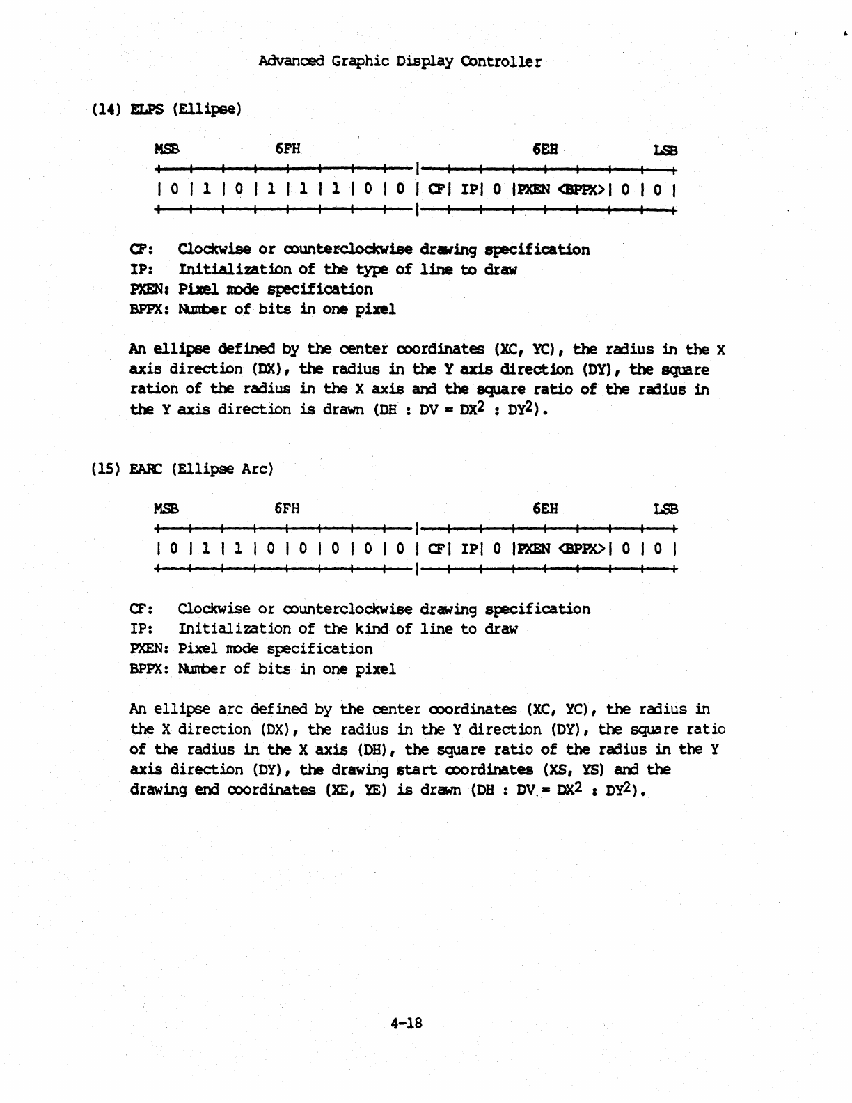
Advanced
Graphic
Display
Controlle
r
(14)
ELPS
(Ellipse)
MSB
6FH
6EB
LSB
+--*--~~--~--~~--+--I--~~~~--~-+--+-~--~
o 1 0 1 1 1 0 0 I
CPI
IPf 0
IP.XEN
<BPf.K>1
0 I 0 I
+-~--~~~~--~-+--+--I--~~~~--~~--+--*--~
0':
Clockwise
or
ex>unterclockw1se drawing
specification
IP:
Initialization
of
the
type
of
line
to
draw
PXEN:
Pixel. node
specification
BPPX:
N.mber
of
bits
in
one
pixel
An
ellipse
defined
by
the
center
ccordinates
(XC,
YC),
the
ra:!ius
in
the
X
axis
direction
(OX),
the
radius
in
the
Y
axis
direction
(DY),
the
square
ration
of
the
radius
in
the
X
axis
and
the
square
ratio
of
the
ra:1ius
in
the
Y
axis
direction
is
drawn
(DB:
DV.
DX2
:
Dy2).
(15)
EAR:
(Ellipse
Arc)
6FH
6EH
LSB
+-~--~~--~--~~--+--I--~~~~--~~--+-~--~
o 1 1 0 0 0 0 0 I
CFI
IPI 0
IP.XBN
<BPP.K>I
0 J 0 I
+-~--~~--~--~~--+--I--~~~~--~~--+-~--~
CF:
Clockwise
or
ex>unterclockwise drawing
specification
IP:
Initialization
of
the
kind
of
line
to
draw
PXEN:
Pixel
node
specification
BPPX:
Nunber
of
bits
in
one
pixel
An
ellipse
arc
defined
by
the
center
<x>ordinates
(XC,
YC),
the
raiius
in
the X
direction
(DX),
the
radius
in
the
Y
direction
(OY),
the
~re
ratio
of
the
radius
in
the
X
axis
(DB)
I
the
square
ratio
of
the
radius
in
the
y
axis
direction
(OY)
I
the
drawing
start
CDOrdinates (XS ,
YS)
~
the
drawing end (X)()rdinates
(XE
,
tE)
is
drawn
(DB:
DV
.•
OX2
:
Dy2).
4-18
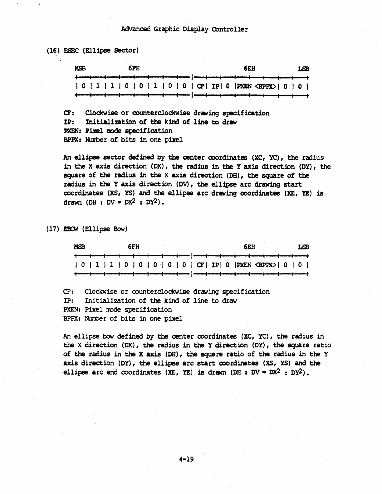
Advanced
Graphic
~isplay
Controlle
r
(16)
ESE)C
(Ellipse
Sector)
MSB
6FH
6EH
LSB
~-*--~~--~--~-P--+--I--~~~~--~~
__
~-+
__
~
o 1 1 0 0 1 0 0 I
CPI
IPI 0
IP.XEN
<BPP.X>I
0
lor
+--'--~~--~--~-P--+--I--~~~~--~~--+--+--~
CF: Clockwise
or
(X)UI'lterclockw!se drawing
specification
!P:
Initialization
of
the
kind
of
line
to
draw
~.:
Pixel
IIDde
specification
BPPX:
R.utbe
r
of
bits
in
one
pixel
An
ellipse
sector
defined
by
the
center
Q)Ordinates
(XC,
te),
the
radius
in
the
X
axis
direction
(OX),
the
radius
in
the
y
axis
direction
(DY),
the
square
of
the
radius
in
the
X
axis
direction
(DB), the
square
of
the
radius
in
the
Y
axis
direction
(DV),
the
ellipse
arc
drawing
start
ex>ordinates
(XS,
YS) and
the
ellipse
arc
drawing cx>ordinates (leE,
!E)
is
drawn
(DB
:
DV
=
DX2
:
Dy2).
(17)
£9:1\7
(Ellipse
Bow)
MSB
6FH
6EH
LSB
+--+--~~--~--~~--+--I--~~~~--~~--+-~--*
o 1 1 0 0 0 0 0 I
CFI
IPI 0
IPKEN
<BPP.K>I
0 0
+--+--~~--~~~~--+--I--~~~~--~~--+-~--~
CF: Clockwise
or
rounterciockwise
drawing
s~ification
IP:
Ini
tialization
of
the
kirxl
of
line
to
draw
P.XEN:
Pixel
mode
specification
BPPX:
Nunt>e
r
of
bits
in
one
pixel
An
ellipse
bow
defined
by
the
center
ooord:inates
(XC,
YC),
the
radius
in
the
X
direction
(OX),
the
radius
in
the
Y
direction
(OY),
the
square
ratio
of
the
radius
in
the
X
axis
(DB),
the
square
ratio
of
the
radius
in
the
Y
axis
direction
(OY),
the
ellipse
arc
start
CXX)rdinates (XS,
YS)
and
the
ellipse
arc
end cx:>ordinates
(XE,
'm)
is
drawn
(DH
: OV.:
OX2
:
Dy2).
4-19
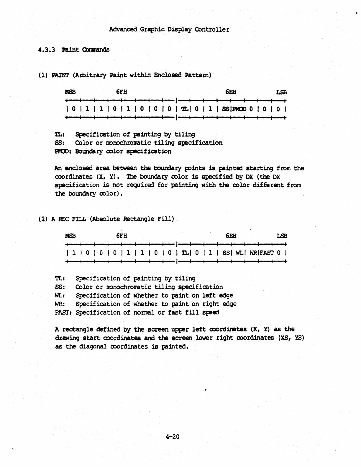
Advanced Graphic
Display
Contro11e r
4.3.3
Paint
Conman:3s
(1) PAIllr (A1:bitrary
Paint
within
Enclosed
Pattem)
MSB
6FH
6EB
LSB
+--+--~~--~--~-P--+--I--~~~~--~~--+--+
__
~
'1
0 1 1 0 1 0 0 I 0 I
TLI
0 I 1 I
SSIPtm
0 I 0 0
+-~--~~~~--~-+--+--I--~~--~~--~~~~~
'It.:
Specification
of
painting
by
Wing
SS:
Color
or
uooochrotratic
tiling
specification
PKD:
Boundary
oolor
specification
An
enclosed
area
between
the
boumaty
p:>ints
is
painted
starting
from
the
(X)()rdinates (X,
Y).
1be
boundary
a:>lor
is
specified
by
OX
(the
OX
specification
is
not
required
for
painting
with
the
a:>lor
different
from
the
boundary
oolor).
(2) A
ROC
FILL (Absolute :Rectangle
Fill)
,
MSB
6FH
6EH
LSB
+--+--~~--~--~~--+--I--~~--~--~-P--+--+--~
1 0 0 0 1 1 0 0 I
TLI
0 I 1 I
sst
WLI
WRfFAST
0
+--+--~~--~--~~--+--.
I--~~--~--~-P--+--+--~
TL:
Specification
of
painting
by
tiling
ss: Color
or
rronochromatic
tiling
specification
WL:
Specification
of
whether
to
paint
on
left
edge
WR:
Bt:ecification
of
whether
to
paint
on
right
edge
FAST:
Specification
of
nornal
or
fast
fill
sp!ej
A
rectangle
defined
by
the
screen
upp!r
left
CDOrdinates
(X,
Y)
as
the
drawing
start
cx>ordinates
and
the
screen
lower
right
Q)()rdinates
(XS,
YS)
as
the
dia~nal
coordinates
is
painted.
4-20
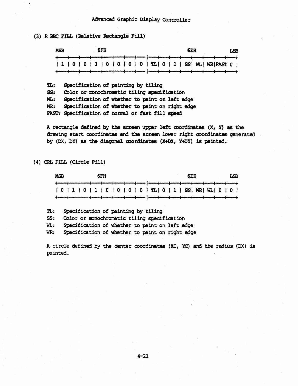
Advanced
Graphic
Display
Contro1le
r
(3) R
~
FILL
(Relative
Rectangle
Fill)
MSB
6FH 6EB
LSB
+--+--+--+--~~--~~--I--~~--~~--~~~~~
1 0 I 0 I 1 I 0 I 0 1 0 I 0 1
!LI
0 1 1 I
SSI
WLI
WRIFAST
0 I
+--+--+--+--'-~--'-~--I--~~--~~--~~~~~
~:
Specification
of
painting
by
tiling
ss:
Q)lor
or
uonochromltic
tiling
specification
WL:
Specification
of
whether
to
paint
on
left
edge
WR:
Specification
of
whether
to
paint
on
right
edge
FAST:
Specification
of
nornal
or
fast
fill
speed
A
rectangle
defined
by
the
screen
upper
left
CX)()rdinates (X, Y)
as
the
drawing
start
coordinates
and
the
screen lower
right
cx>ordinates generatED
by
(OX,
DY)
as
the
diacpnal
ax>rdinates
(X+OX,
Y-tDY)
is
painted.
(4)
CRL
FILL
(Circle
Fill)
MSB
6FH
6EH
LSB
+--+--+-~--+-~I-,
~--+--I--~~--~~--~~~~~
o 1 0 1 0 0 0 0 I
TLI
0 I 1 I
SSl
WRI
WoL(
0 0
+--+--+-~--+-~--+--+--I--~~--~~--~~~~~
TL:
Specification
of
painting
by
tiling
ss:
Color
or
rronochronatic
tiling
specification
WL:
Specification
of
whether
to
paint
on
left
edge
WR:
Specification
of
whether
to
paint
on
right
edge
A
circle
defined
by
the
center
coordinates
(XC,
YC)
anl
the
radius
(DX)
is
painted.
4-21
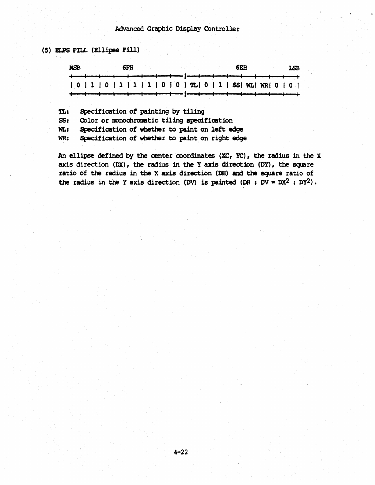
Advanced
Graphic
Display
Controlle
r
(5)
ELPS
FILL
(Ellipse
Pill)
MSB
6FB
6EH
LSB
+--+--+--+--+--+--+--+--I--~~--~~~~~~~~
o 1 0 1 I 1 I 1 0 0 I
'lL1
0 I 1 I
sst
WLI
WRI
0 I 0 I
+--+--+--+--+--+--+--+--I--~~--~~--~~~~~
'!L:
Specification
of
painting
by
tiling
SS: Color
or
DDnochromtic
tiling
specification
WL:
Specification
of
whether
to
paint
on
left
edge
WR:
Specification
of
whether
to
paint
on
right
edge
An
ellipse
defined
by
the
center
coordinates
(XC,
l'C),
the
radius
in
the
X
axis
direction
(DX),
the
radius
in
the
Y
axis
c3irection
(Dy),
the
square
ratio
of
the
radius
in
the
X
axis
direction
(DB)
am
the
square
ratio
of
the
radius
in
the
Y
axis
direction
(DV)
is
painted
(DB
:
DV.
Dx2 :
Dy2).
4-22
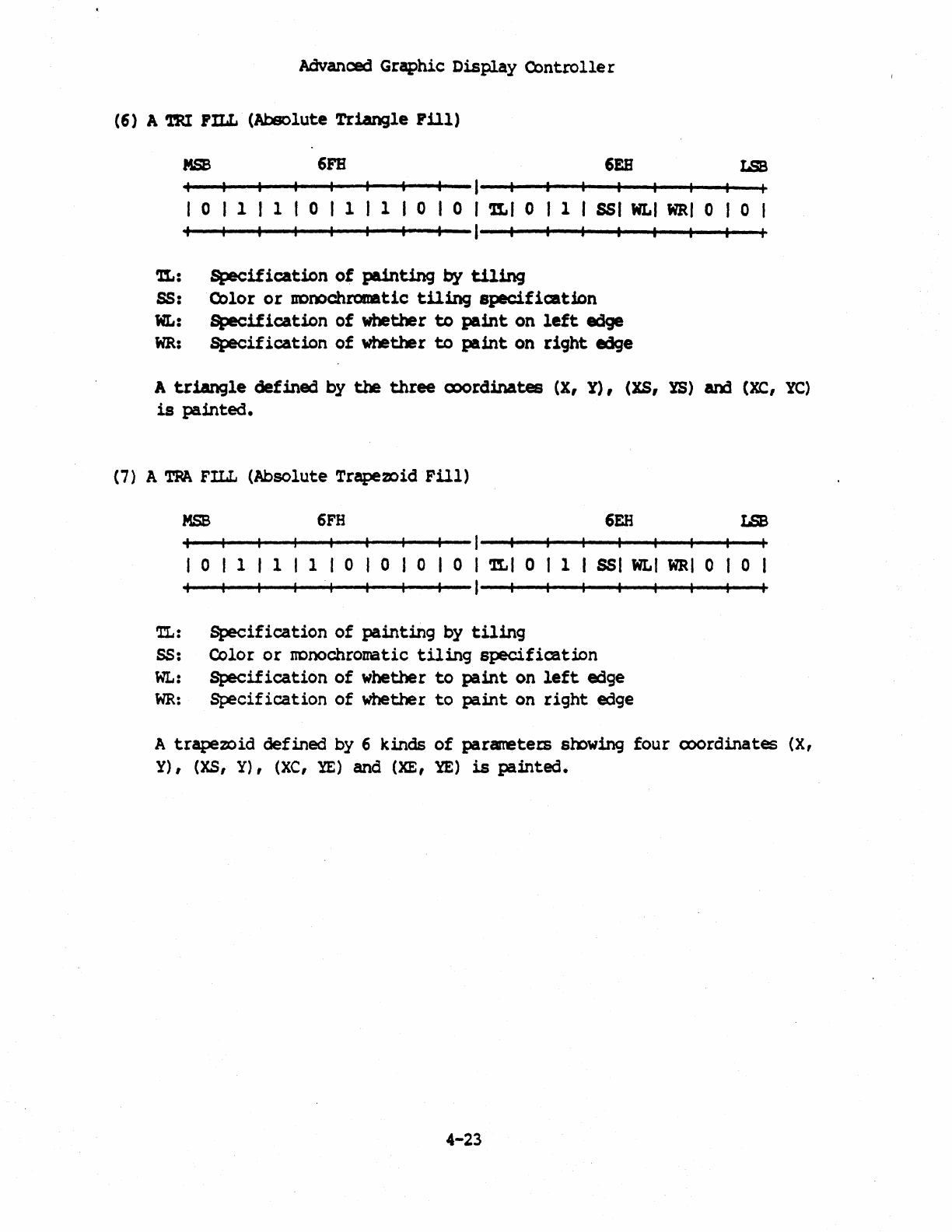
Advanced
Graphic
Display
Controlle
r
(6) A 'l'RI PnaL
(Absolute
Triangle
P111)
MSB
6FB
6EB
LSB
+--+--+-~--+-~--~~--I
I
Oil
I 1 0 1 1 I 0 I 0 I
~I
0 I 1 I
SSI
WLI
WRI
0 I 0 I
+--+--+--+--+--+--+--+--I--~~--~~--~~~~~
'I'L:
Specification
of
painting
by
tiling
ss:
Q)lor
or
uo1))chromatic
tiling
specification
WL:
6\leCification
of
whether
to
paint
on
left
edge
WR:
6\leCification
of
whether
to
paint
on
right
edge
A
triangle
defined
by
the
three
cx>ordinates
(X,
Y), (XS,
!S)
am
(XC,
YC)
is
painted.
(7)
A
TPA
FILL (Absolute
Trapemid
Fill)
MSB
6FH
6EH
LSB
+--+--+--+--+--+--+--+--I--~~--~~--~~~~~
o 1 1 1 0 0 0 0 I
'I'Ll
0 I 1 I
sst
WoLI
WoRI
0 I 0 I
I
I--~~--~~--+-~--+--+
TL:
Specification
of
painting
by
tiling
ss: Color
or
nonochromatic
tiling
specification
WL:
Specification
of
whether
to
paint
on
left
edge
WR:
Specification
of
whether
to
paint
on
right
edge
A
trapemid
defined
by
6
kinds
of
parametem
soowing
four
cx>ordinates
(X,
Y),
(XS,
Y),
(XC,
~)
and (XE,
YE)
is
painted.
4-23
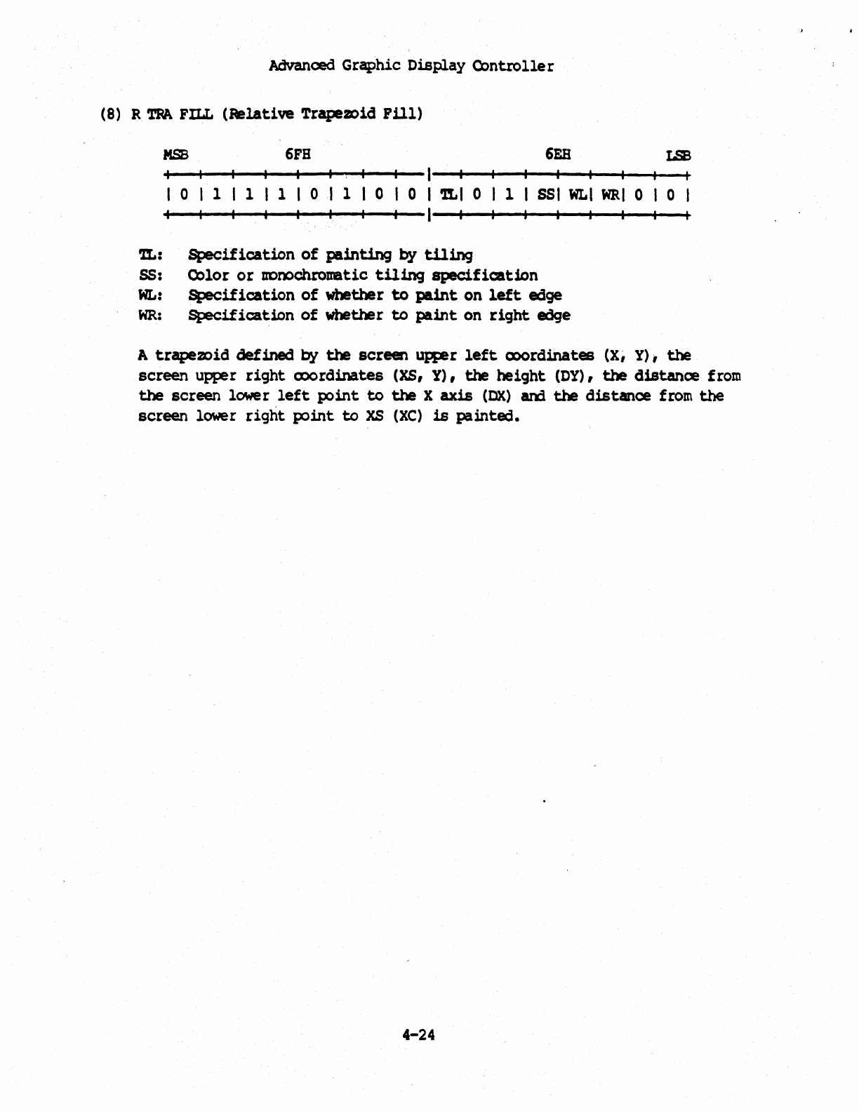
Advanced
Graphic
Display
Controlle
r
(8) R
TPA
FILL
(Relative
'l'rapefDid
Fill)
MSB
6FH
6EH
LSB
+--+--+--+--~~~+--+--I--~~--~~--~~~~-*
o 1 1 1 0 1 I 0 I 0 I
'I'Ll
0 I 1 I
SSI
WLI
WRI
0 I 0
+--+--+--+--+-~--+-~--I--~~--~~--~~~~~
TL:
Specification
of
painting
by
tiling
ss:
Color
or
uonochromatic
tiling
specification
WL:
Specification
of
whether
to
paint
on
left
edge
WR:
Specification
of
whether
to
paint
on
right
edge
A
trapemid
defined
by
the
screen
uR2r
left
cx>ordinates (Xi
Y),
the
screen upper
right
(X)()rdinates (XS,
Y),
the
height
(DY),
the
distance
from
the
screen
lower
left
point
to
the
X
axis
(OX)
am
the
distance
from
the
screen lower
right
point
to
XS
(XC)
is
painted.
4-24
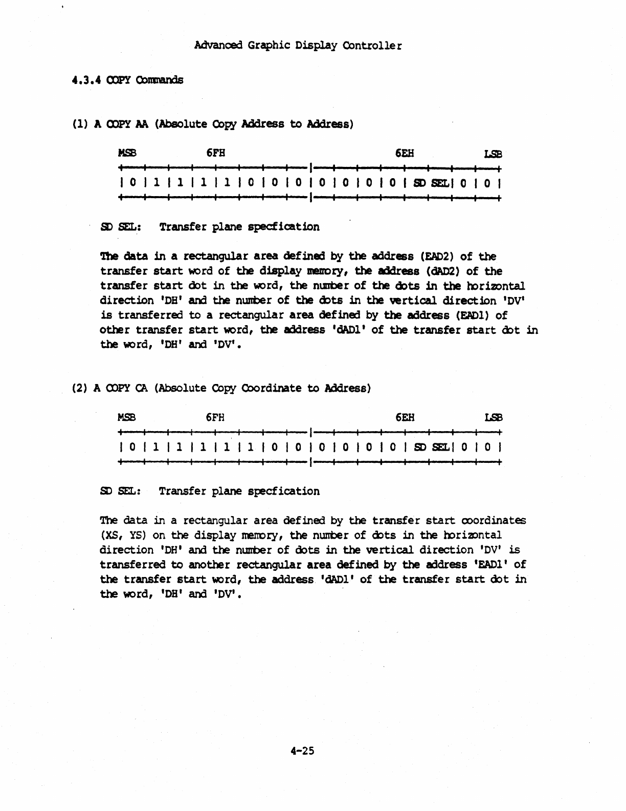
Advanced
Graphic
Display
Cantrolle
r
4.3.4
CXlPY
Q)ltINll'¥1s
(1) A
CXlPY
AA
(Absolute
Copy
Address
to
Address)
MSB
6FB
6EH
LSB
o 1 1 1 1 0 0 0 0 I 0 I 0 I 0 I
SO
SELl
0 I 0 I
~
BEL:
Transfer
plane
specfication
'!be
data
in
a
rectangular
area
defined
by
the
address
(EAD2)
of
the
transfer
start
word
of
the
display
mezrory,
the
address (cWl2)
of
the
transfer
start
dot
in
the
word,
the
nUllber
of
the
cbts
in
the
b::>ri2'Dntal
direction
'DB'
and
the
nunber
of
the
cbts
in
the
vertical.
direction
'DV'
is
transferred
to
a
rectangular
area
defined
by
the
address
(FADl)
of
other
transfer
start
word,
the
address 'c:Wll'
of
the
transfer
start
Cbt
in
the
word, 'DB' and 'DV'.
(2) A
cx)PY
CA
(Absolute
Copy
Coordinate
to
Address)
MSB
6FH
6EH
LSB
+--+--~~--~--~~--+--I--~~~~--~~--+-~--~
o 1
III
1 1 0 0 I 0 I 0 I 0 I 0 I
SO
SELl
0 0
+--+--~~--~--~~--+--I--~~--~--~~--+-~--~
so
BEL:
Transfer
plane
specfication
The
data
in
a
rectangular
area
defined
by
the
transfer
start
(X)ordinates
(XS,
YS)
on
the
display
nerrory,
the
nunDer
of
cbts
in
the
rori2Pntal
direction
'DH'
and
the
n&.mt>er
of
dots
in
the
vertical
direction
'DV'
is
transferred
to
another rectangular
area
defined
by
the
aldress
'EADl'
of
the
transfer
start
word,
the
address
'd1\Dl'
of
the
transfer
start
dot
in
the
word, 'DB' and 'DV'.
4-25
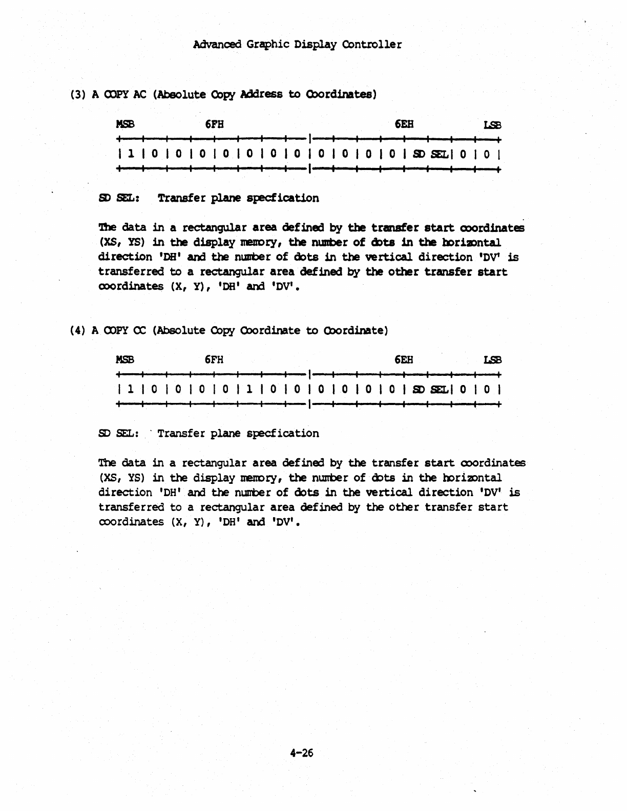
Advanced
Graphic
Display
Controller
(3)
A
CDPY
AC
(Absolute
Copy
Address
to
Q)ordinates)
MSB
6FB
6EB
1 0 0 0 0 0 0 0 0 0 0 I 0 I
SO
SELl
0 I 0
SD
SEL:
Transfer
plane
sp!Cfication
b
data
in
a rectangular
area
defined
by
the
transfer
start
Q)()rd.inates
(XS, YS)
in
the
display
neuory,
the
nusrber
of
~ts
in
the
mrimntal
direction
'DB'
and
the
nUDber
of
dots
in
the
vertical
direction
'DV'
is
transferred
to
a
rectangular
area
defined
by
the
other
transfer
start
(X)()rdinates (X,
Y),
'OB' and 'DV'.
(4)
A
OJPY
ex:
(Absolute Copy
())ordinate
to
Q)ordinate)
MSB
6FH
6EB
LSB
1 0 0 0 0 1 0 0 0 0 I 0 I 0 I
SO
SELl
0 0
so
BEL:
.
Transfer
plane
specfication
'!be
data
in
a
rectangular
area
defined
by
the
transfer
start
cx>ordinates
(XS,
YS)
in
the
display
nenory,
the
nwrber
of
(bts
in
the
mri2Dntal
direction
'DH'
and
the
nUlI'ber
of
dots
in
the
vertical
direction
'DV'
is
transferred
to
a
rectangular
area
defined
by
the
other
transfer
start
ooordinates
(X,
Y),
'DB'
and 'DV'.
4-26
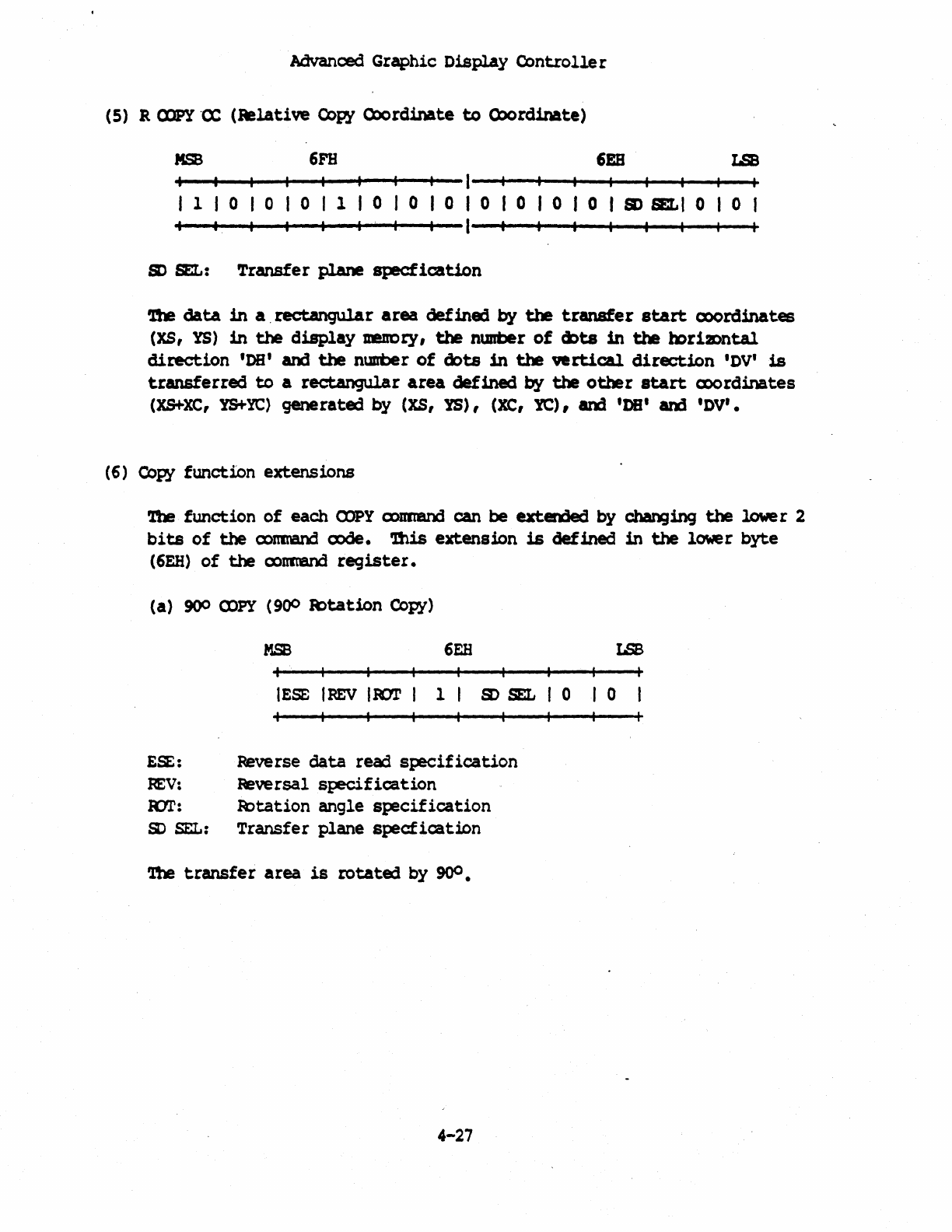
Advanced
Graphic
Display
Controlle
r
(5)
R Q)PY'OC
(Relati
\Ie
Copy
Q)ordinate
to
Q:)ordinate)
MSB
6FH
6£8
+--+--+--+--~~--~~--I--~~--~~--~~~~-*
I 1 I 0 I 0 I 0 I 1 I 0 I 0 I 0 I 0 I 0 I 0 I 0 I
SO
SELl
0 I 0 I
+--+--+-~--~~--~~--l--~~--~~--~~~~-+
so
BEL:
Transfer
plane
specfication
The
data
in
a.
rect:angul.ar
area
defined
by
the
transfer
start
(X)()rdinates
(XS, YS)
in
the
display
meucry,
the
nunber
of
cbts
in
the
bori2Dntal
direction
'DB' and
the
DUllber
of
cX>ts
in
the
ftrt1cal
direction
'DV'
is
transferred
to
a rect.angul.ar
area
defined
by
the
other
start
cx>ordinates
(XS+XC,
YS+YC)
generated
by
(xs,
YS),
(XC, 1'C),
am
'DB'
am
'DV·.
(6)
Copy
function
extensions
The
function
of
each
OOPY
ammand can be extended
by
changing
the
lower
2
bits
of
the
ooll1liUld
code.
ibis
extension
is
defined
in
the
lower
byte
(6EH)
of
the
oomend
register.
(a)
9()0
(X)PY
(9oo
a>tation
Copy)
MSB
6EH
LSB
lESE
IREV
lIar
I 1
&>
SEL
I 0 0
ESE: Reverse
data
read
specification
REV:
Reversal
specification
ROT:
~tation
angle
specification
S)
SEt:
Transfer
plane
specfication
'!be
transfer
area
is
rotated
by
9()0.
4-27
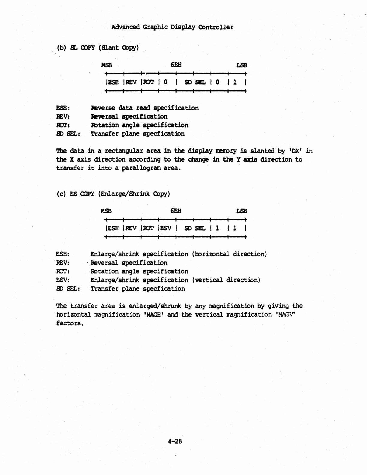
Advanced
Graphic
Display
Q:)ntrolle
r
(b)
SL
CDPY
(Slant
Copy)
ESE:
REV:
101':
S> SEL:
MSB
6EB
I .
I.
lESE
I
REV
1R11'
I 0
S)
BEL
0
Jeverse
data
read
specification
Reversal
specification
R:>tation
angle
specification
Transfer
plane
specfication
LSB
1
'!'he
data
in
a
rectmlgular
area
in
the
display
DlmDty
is
slante3
by
'DX'
in
the
X
axis
direction
accx>rding
to
the
change
in
the
y
axis
direction
to
transfer
it
into
a
parallogrmn
area.
(c)
ES
CDPY
(Enlarqe/Shrink
Copy)
EBB:
.
REV:
ESV:
S>
BEL:
MSB
6EH
LSB
IESH
IREV
1K1l'
IESV
I
s>
SEL
1 1
Enlarge/shrink
specification
(horizontal
direction)
,
Reversal
specification
~tation
angle
specification
Enlarge/shrink
specification
(vertical
direction)
Transfer
plane
specfication
The
transfer
area
is
enlarged/shrunk
by
any
magnification
by
giving
the
h:>rizontal.
magnification
'MAGS'
aOO
the
vertical
magnification
1M1(;V'
factors.
4-28
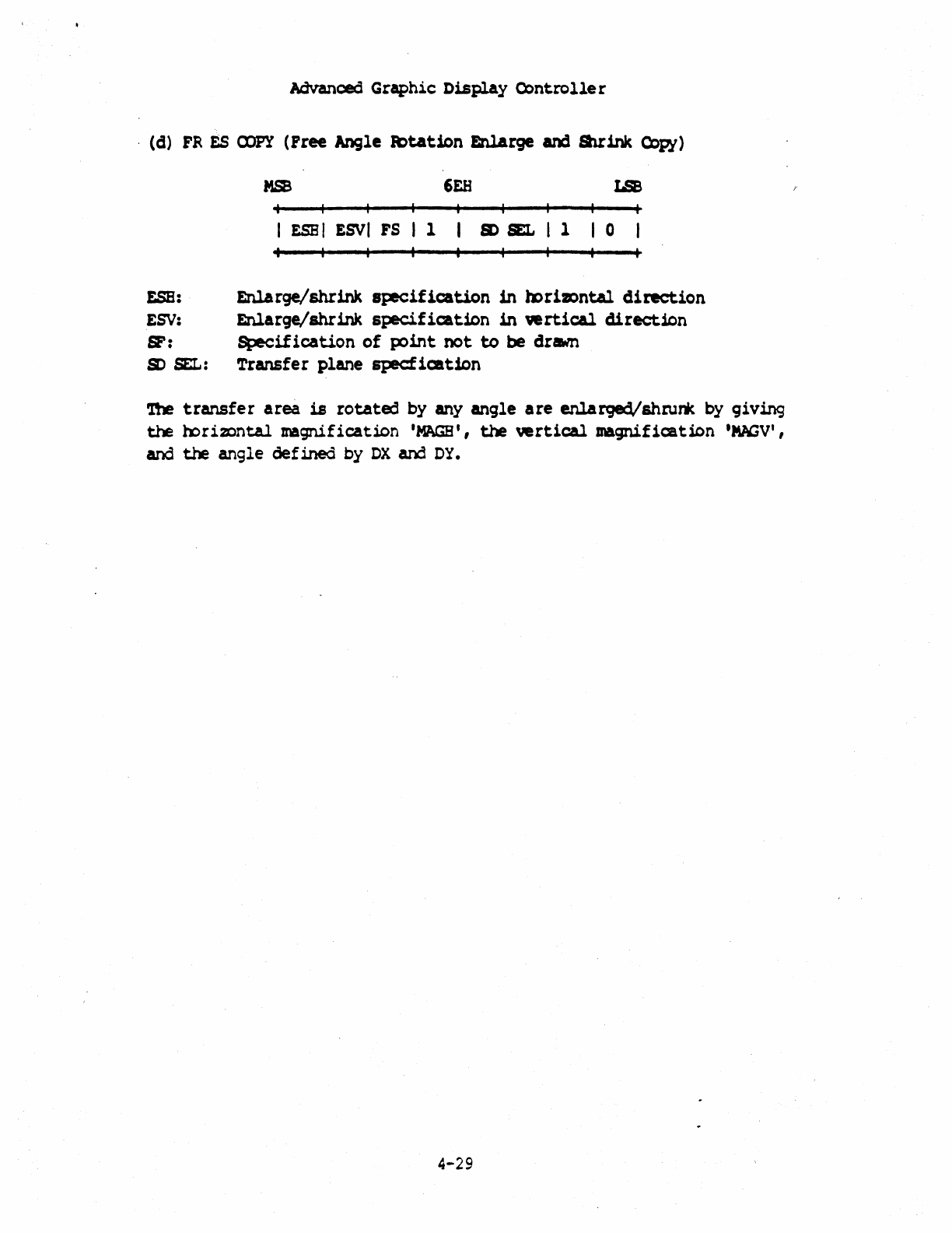
Advanced Graphic
Display
Controlle
r
.
(a)
FR
ts
C'JJP'i
(Free
Angle It>tAtion
Enlarge
ana
Slrink
Copy)
MSB
6EH
IS
I
ESE
I
ESVI
FS
I 1
s)
BEL
I 1 0
EBB:
Enlarge/shrink
specification
in
mrilDntal
direction
ESV:
Enlarge/shrink
specification
in
vertical
direction
SF:
~ification
of
point
not
to
be
dram
s)
BEL:
Transfer
plane
specfication
'!be
transfer
area
is
rotated
by
any
angle
are
enlarged/shrurK
by
giving
the
rori20ntal
magnification
'MAGS',
the
vertical
magnification
'MAGV',
and
the
angle
def
ined
by
DX
and
DY.
4-29
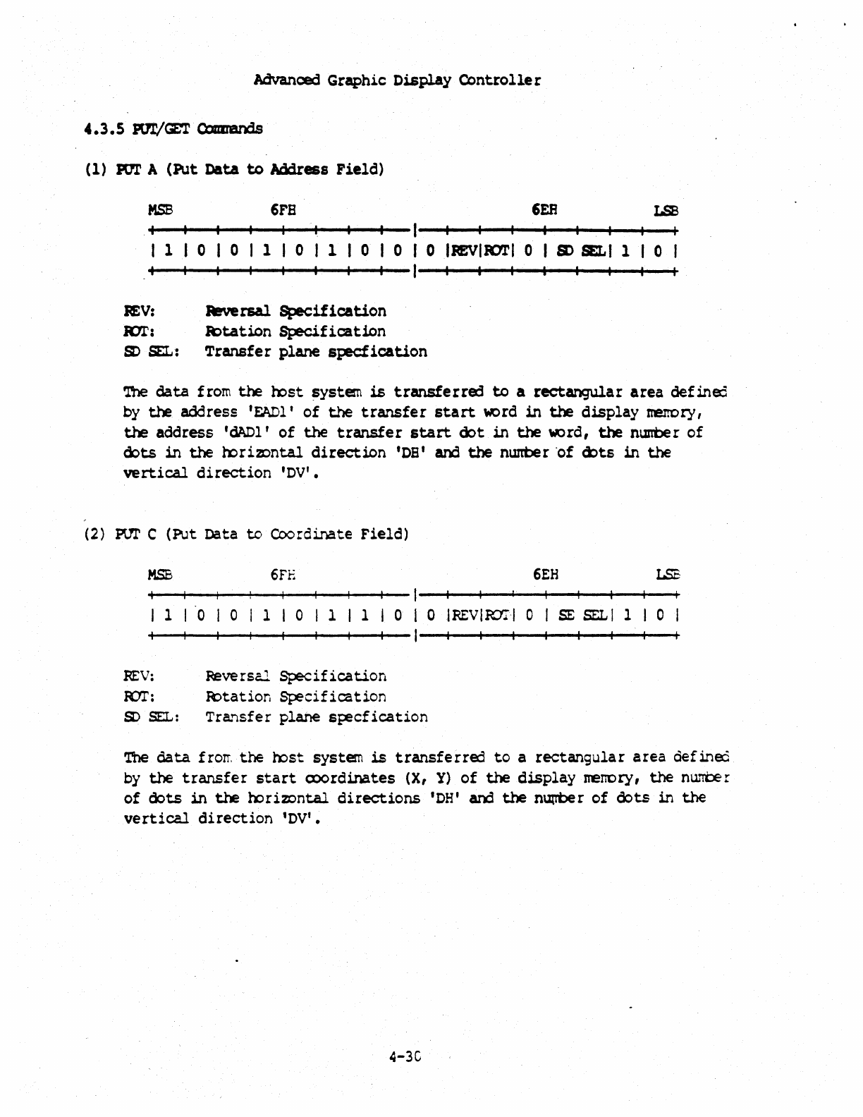
Advanced
Graphic
Display
Controlle
r
4.3.5
IVr/CET Q:mre.nds
(1)
Pm' A
(Put
Data
to
Address
Field)
MSB
6FB
6EB
LSB
.1
I--~-+--+--+--~~--~~
1 0 0 1 0 1 0 0 I 0 I
REV
I
JOT
I 0 I
SO
SELl
1 I 0 I
+-~--~~~~--~-P--+--I--~~~~--~~--+--+--~
EV:
Reversal
Specification
K1r:
It>tation
Specification
s)
BEL:
Transfer
plane
st:eCfication
~
data
from
the
rost
system
is
transferre:1
to
a
rectangular
area
define:
by
the
address
'EAD1'
of
the
transfer
start
word
in
the
display
mernory,
the
address 'cW)1'
of
the
transfer
start
dot
in
the
word,
the
nun'ber
of
cX>ts
in
the
rori2Ontal
direction
'DB' and
the
nwrber ·of
ci::>ts
in
the
vertical
direction
'OV'.
(2)
PUT
C
(Put
Data
to
Coordinate
Field)
MSB
6FE
6EH
1 0 0 1 0 1 1 0 0 I
REV
I
IDT·I
0 I
SE
SEL
I 1 0
REV:
Reversal
Specification
~:
~tation
Specification
SO
SEL:
Tra~sfer
plane
specfication
The
data
frorr,
the
mst
system
is
transferred
to
a
rectangular
area
defin~
by
the
transfer
start
ex>ordinates
(X,
Y)
of
the
display nenory,
the
nlli10e
r
of
oots
in
the
l'x:>rimntal
directions
'OH' and
the
nUfl'ber
of
dots
in
the
vertical
direction
'OV'.
4-3C
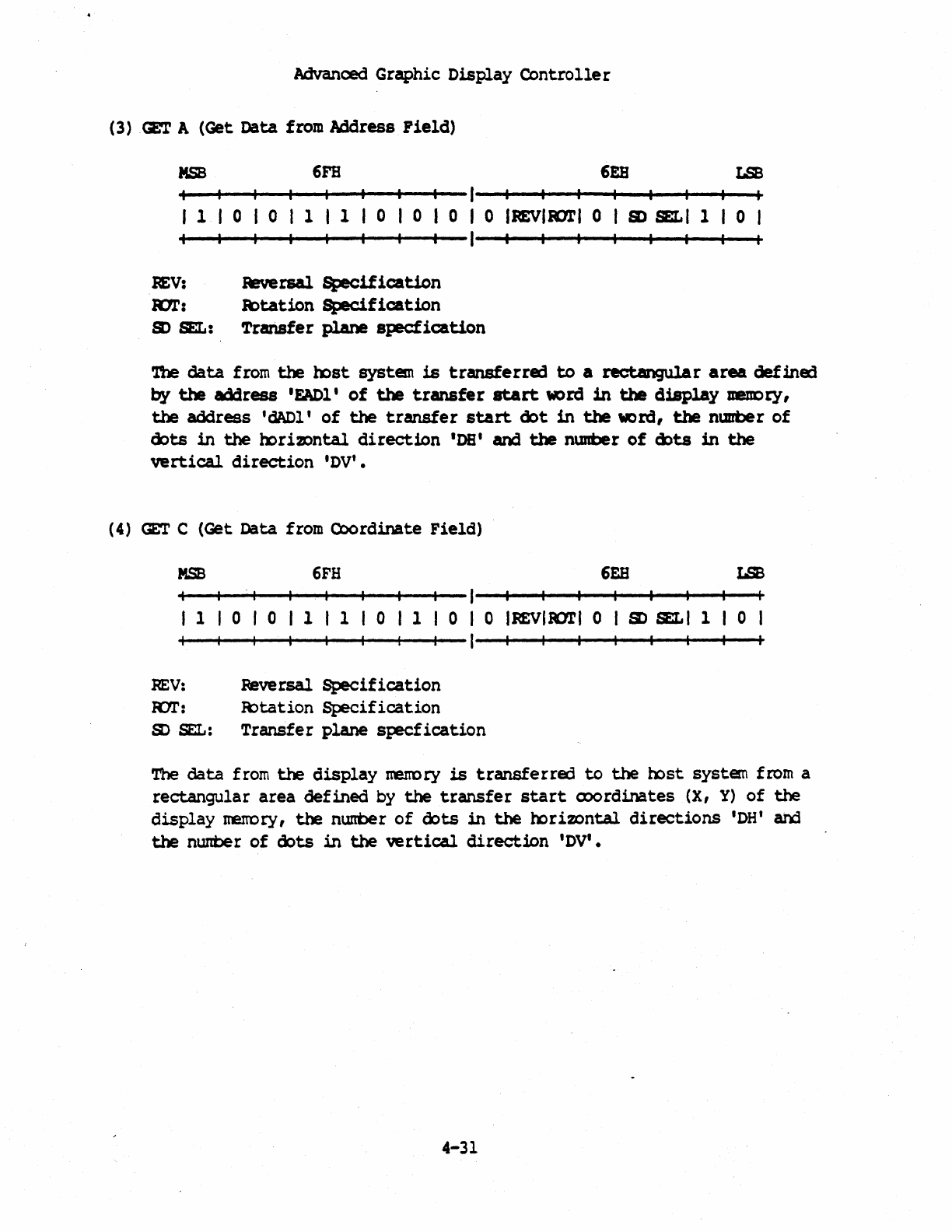
Advanced
Graphic
Dis~ay
Controller
(3)
GET
A
(Get
Data
from Address
Field)
MSB
6FB
6EB
LSB
I 1 I 0 I 0 1 1 0 0 0 0
IREVliOTl
0 I
SO
SELl
1 I 0
REV:
Reversal
Specification
R:7l':
R)tation
Specification
s)
SEL:
Transfer
plane
specfication
'!be
data
from
the
mst
system
is
transferred
to
a
rectangular
area
def1ned
by
the
address
'FADl'
of
the
transfer
start
word
in
the
display
meucry,
the
address
'dADl'
of
the
transfer
start
oot
in
the
we
I'd,
the
nuube r
of
oots
in
the
horiz:>ntal
direction
'DB' and
the
nunber
of
ebts
in
the
vertical
direction
'DV'.
(4)
GET
C
(Get
Data
from
Coordinate
Field)
MSB
6FH
6EB
LSB
-r
1 0 0 1 1 0 1 0 0
IREVIRDTI
0 I
SO
SELl
1 0
REV:
Peversal
Specification
IUI':
lC:>tation
Specification
SO
BEL:
Transfer
plane
specfication
The
data
from
the
display
menory
is
transferred
to
the
b:>st system from a
rectangular
area
defined
by
the
transfer
start
cx>ordinates
(X,
Y)
of
the
display
nerrory,
the
nwrber
of
oots
in
the
horizontal
directions
'DH'
arxl
the
nun:ber
of
cbts
in
the
vertical
direction
IDV'.
4-31
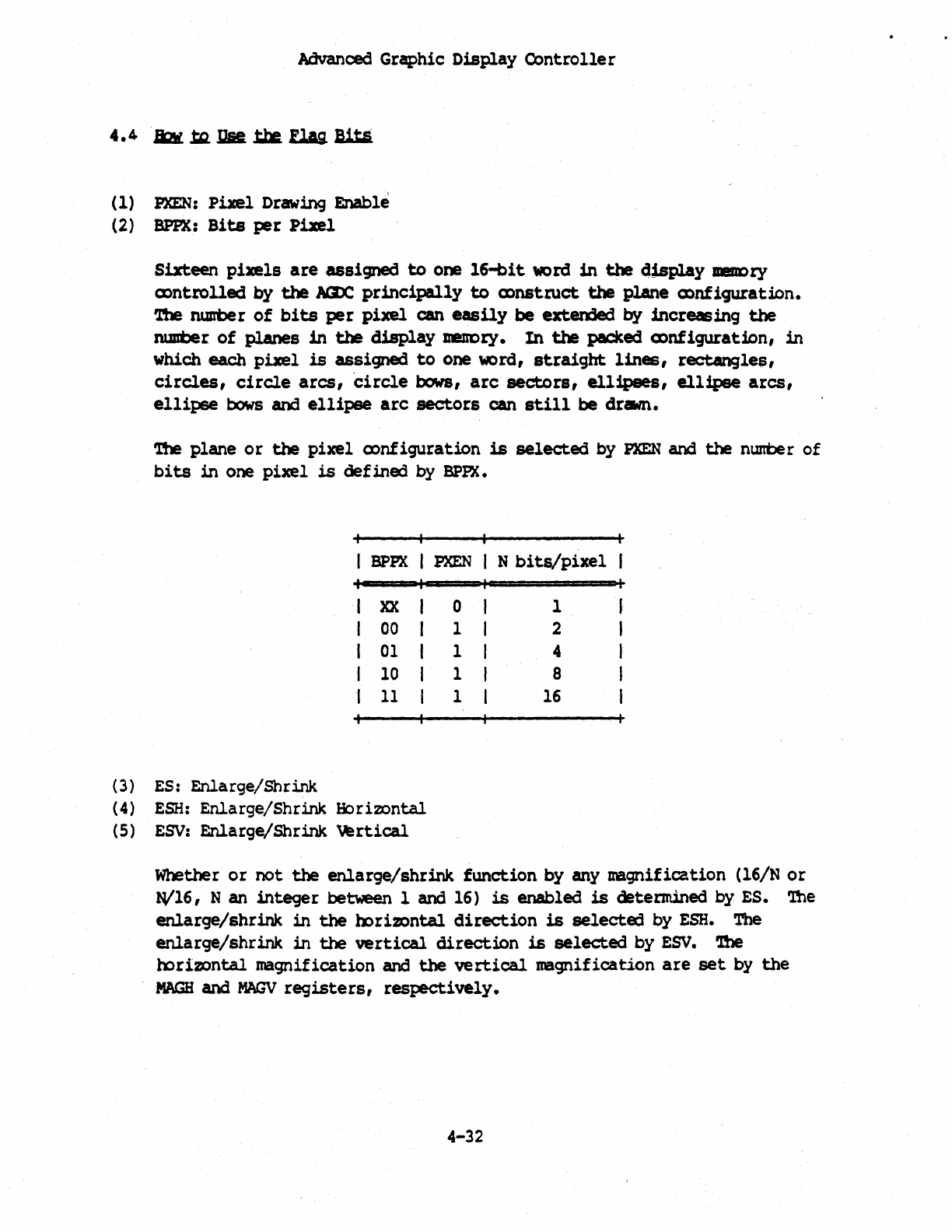
Advanced
Graphic
Display
Controller
(l)
PXEN:
Pixel
Drawing
Enable
(2)
BPPX:
Bits
per
Pixel
Sixteen
pixels
are
assignecl
to
one
16-bit
word
in
the
41splay IlleDDry
(X)ntrolled by
the
AaX;
principally
to
mnsttuct
the
plane
mnfiguration.
1'be
ru.urDer
of
bits
per
pixel
can
easily
be exten3ed
by
increasing
the
ru.urDer
of
planes
in
the
display
JreUDry.
In
the
packed (X)nfiguratiDn,
in
which
each
pixel
is
assigned
to
one
word,
straight
lines,
rectangles,
circles,
circle
arcs,
'circle
bows,
arc
sectors,
ellipses,
ellipse
arcs,
ellipse
bows
and
ellipse
arc
sectors
can
stUl
be
drawn.
'l!le
plane
or
the
pixel
oonfiguration
is
selected
by
PXEN
and
the
nunber
of
bits
in
one
pixel
is
defined
by
BPPA.
I
BPPX
I
PXEN
I N
bits/pixel
I
XX
00
01
10
11
(3) ES: Enlarge/Shrink
(4)
ESH:
Enlarge/Shrink
Horizontal
(5)
ESV:
Enlarge/Shrink
~rtical
0 1
1 2
1 4
1 8
1
16
Whether
or
not
the
enlarge/shrink
function
by any
magnification
(16/N
or
Wl6,
N an
integer
between 1
and
16)
is
enabled
is
determined by ES. 'Ihe
enlarge/shrink
in
the
mrimntal
direction
is
selected
by
ESH.
The
enlarge/shrink
in
the
vertical
direction
is
selected
by
ESV.
'nle
horizontal
magnification
and
the
vertical
magnification
are
set
by
the
MAGH
and
MAGV
registers,
respectively.
4-32
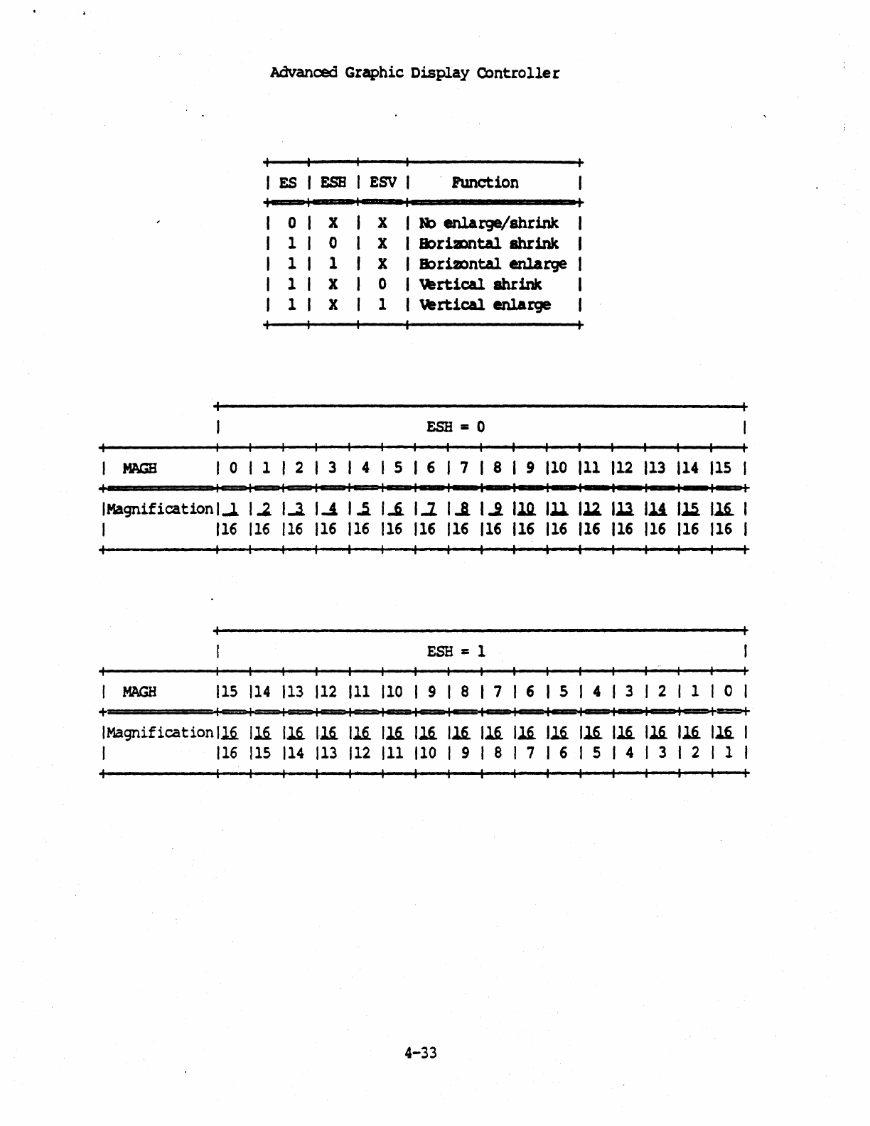
Advanced Graphic
Display
Controlle
r
I
ES
I
EBB
1
ESV
I Function
o I X I X I R;)
enlarge/shrink
1 1 0 I X I
It)rimntal
shrink
1 I 1 I X I
8:)rimntal
enlarge
1 I X I 0 I
~rtical
shrink
1 I X 1 1 I
vertical
enlarge
ESH
= 0
IMagnificationl..l 1
~
1....3.
1-4
1..5.
1..6.
1..2.
I..&.
l...i
1lQ.
III
In
III
Jli
I~
III
I
1
116
116
116
116
116 116
116
116
116
116
116
116
116
116 116
116
I
ESH
= 1 I
..
MAGS
115
114
113
112
III
110
I 9 1 8 I 7 1 6 I 5 1 4 I 3 1 2 I 1 I 0 I
+==~==~=*~+=~~~~~c=~=*c=+=~-=~~~~~=*~~=+
I Magnif
ication
112.
IJ&
lli
lli
116.
lli
116.
116.
lli
lli
1M
116.
I~
lli
1l6.
Il§. I
1
116
115 114 113
112
III
110
I 9 I 8 1 7 I 6 I 5 I 4 I 3 I 2 I 1 I
4-33
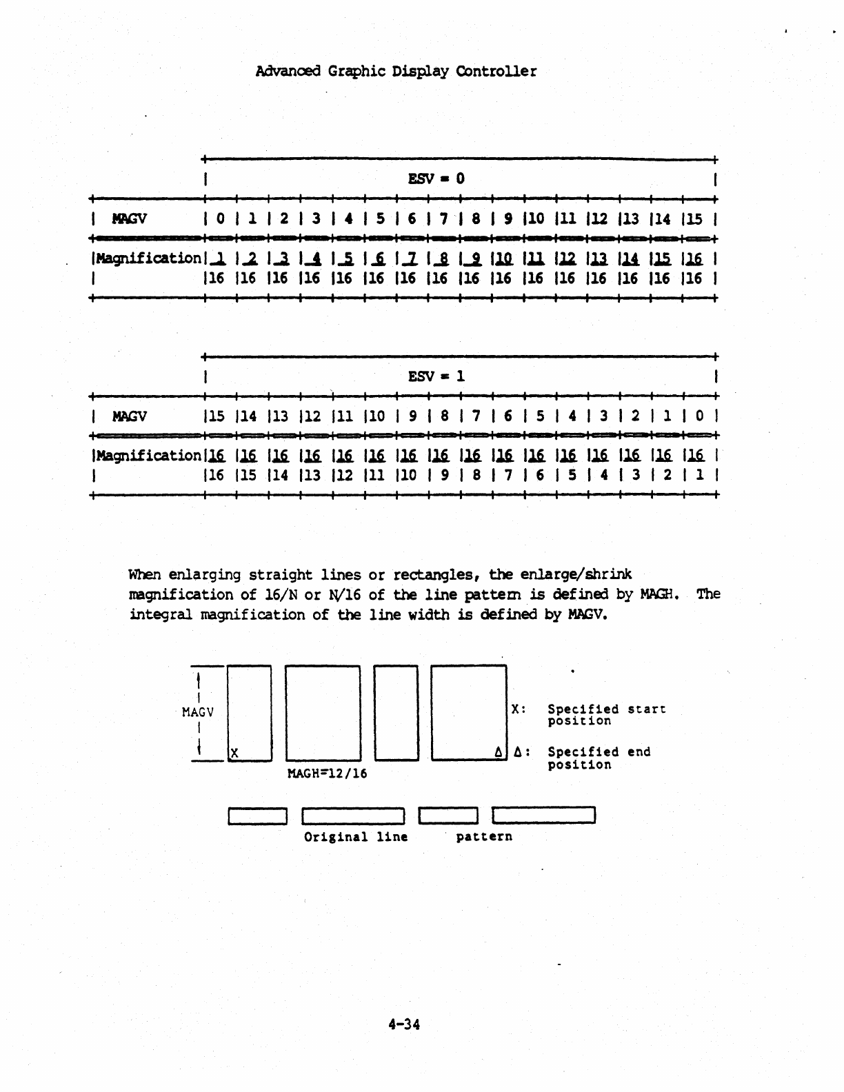
Advanced
Graphic
Display
Controller
~
I 0 I 1 I 2 I 3 I 4 I 5 I 6 I 7 I 8 I 9
110
III
112
113
114
115
I
+
IMagnification I
~
1...1
I..J.
I..J I
~
l.i
J.l
1.1
1..1
IlJI.
III
1l2.
III
1M
Il.S.
1l6.
I
I
116
116
116
116 116 116
116
116 116
116
116 116 116
116
116 116
I
ESV.
1
~
115
114
113
112
III
110
I 9 I 8 I 7 I 6 I 5 I 4 1 3 I 2 I 1 0
IMagnif
ication
Il&.
1l6.
116.
116.
116. 116.
lli
116.
lli
lli
lli
116.
116.
116.
1l6.
1l6.
I
1
116
115
114
113 112
III
110
I 9 I 8 I 7 I 6 I 5 I 4 I 3 I 2 I 1 I
When
enlarging
straight
lines
or
rectangles,
the
enlarge/shrink
magnification
of
l6/N
or
W16
of
the
line
pattem
.
is
defined
by
MAGH.
The
integral
magnification
of
the
line
width
is
defined
by
MN3V.
1
I
MAG
V
I
t
x.
X:
MAGH=12/l6
Specified
start
position
Specified
end
position
_________ 1 I I
I~
______
~
Original
line
.
pattern
4-34
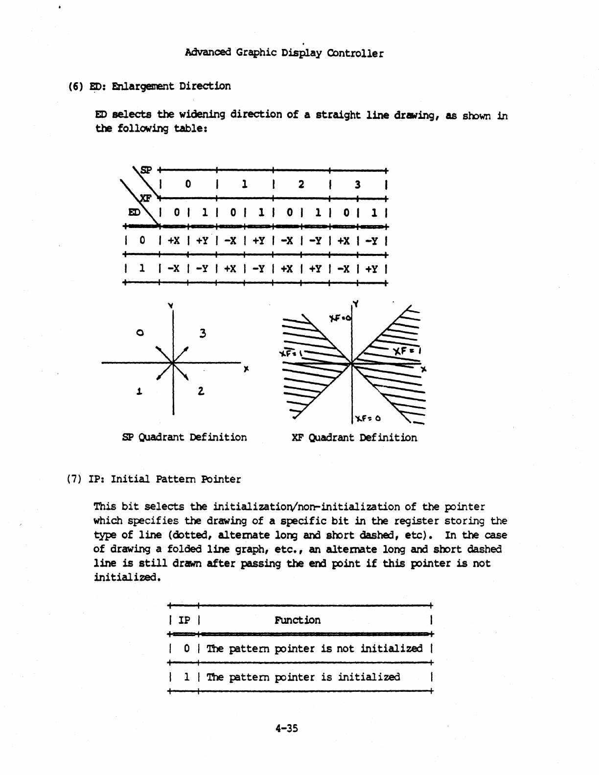
Advanced
Graphic
Display
Controlle
r
(6)
E;D:
Enlargement
Direction
ED
selects
the
widening
direction
of
a
straight
line
drawing,
as
soown
:1.n
the
following
table:
o 1 2 3
o 1 o 1 o 1 o 1
o I
+x
I
+y'
I -x I
+Y
I -x I -Y I
+X
I
-Y
I
o 3
1
2.
~hO~~
SP
Quadrant
Definition
XF
Quadrant
Definition
(7)
IP:
Initial
Pattern
Pointer
This
bit
selects
the
initialization/non-initialization
of
the
p::>inter
which
specifies
the
drawing
of
a
specific
bit
in
the
register
storing
the
type
of
line
(dotted,
altemate
long
and
srort
dashed,
etc).
In
the
case
of
drawing a
folded
line
graph,
etc.,
an
alternate
long
and
srort
dashed
line
is
still
drawn
after
passing
the
erd
point
if
this
pointer
is
not
initialized.
IP
Function
o I
The
pattern
pointer
is
not
initialized
1
The
pattern
pointer
is
initialized
4-35
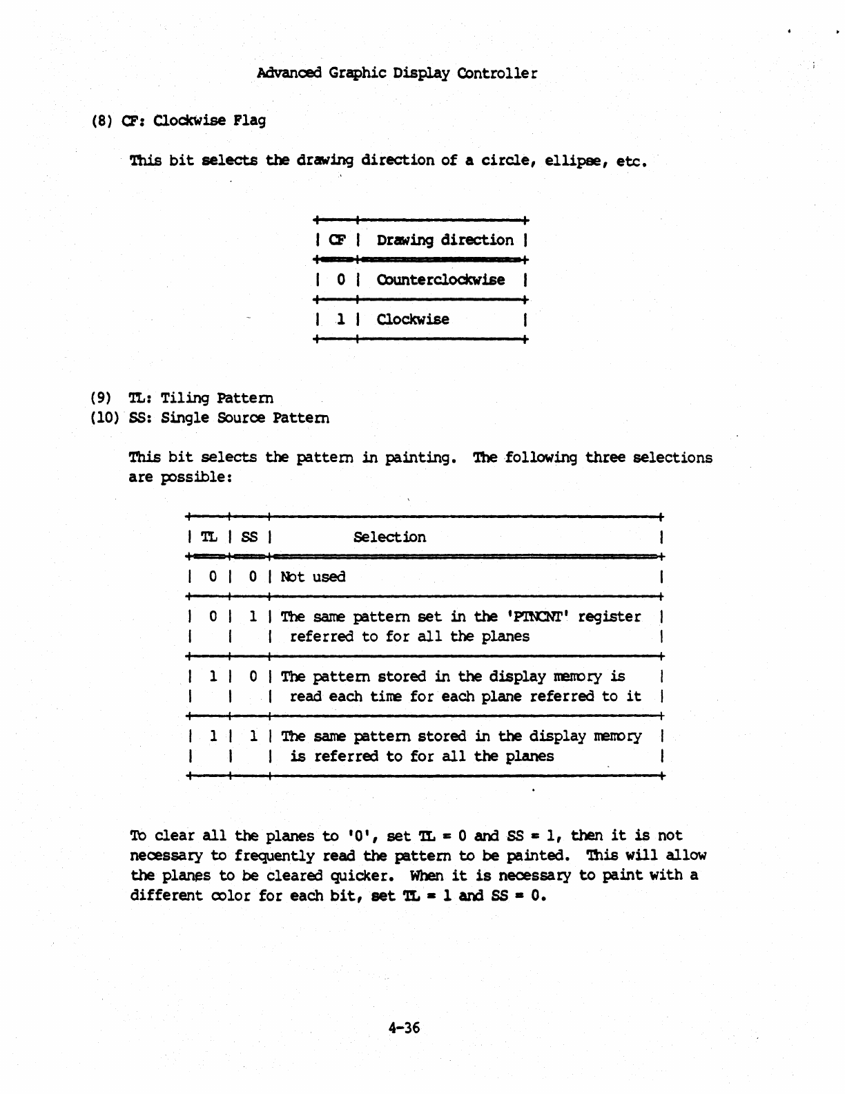
Advanced
Graphic
Dis~y
Controller
(8)
CF:
ClockWise
Flag
'Ibis
bit
selects
the
drawing
direction
of
a
circle,
ellipse,
etc.
I
CF
I Drawing
direction
I
o
Oounter~ise
1 Clockwise
(9)
TL:
Tiling
Pattem
(10) SS:
Single
Source
Pattem
This
bit
selects
the
pattern
in
painting.
'!be -following
three
selections
are
p:>ssible:
TL
SS
Selection
0 0 I
~t
used
0 I I
The
same
pattem
set
in
the
• P.IN:Nr I
register
I
referred
to
for
all
the
planes
I 0 I
The
pattern
stored
in
the
display
menory
is
I
read
each
tine
for
each
plane
referred
to
it
I 1
The
same
pattem
stored
in
the
display
rrerrory
is
referred
to
for
all
the
planes
To
clear
all
the
planes
to
• 0 I,
set
TL
I:
0
andSS
I:
1,
then
it
is
not
necessary
to
frequently
read
the
p:lttern
to
be
painted.
'!his
will
allow
the
planes
to
be
cleared
quicker.
When
it
is
necessary
to
paint
with
a
different
oolor
for
each
bit,
set
TL
• 1
aoo
SS
•
o.
4-36
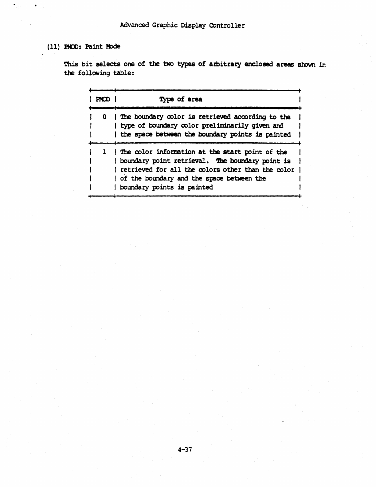
Advanced
Graphic Display
Controller
(11)
IKD:
Paint
ftt>de
This
bit
selects
one
of
the
two
types
of
amitraty
enclosed areas slxNn
in
the
following
table:
I Pta> I
~
of
area
o I 'Ibe
boundary
oolor
is
retrieved
according
to
the
I
type
of
boundaty
color
preliminarily
qiven
and
I
the
space between
the
boundary
points
is
painted
1 I '!be
color
info
mat
ion
at
the
start
point
of
the
I
boundary
plint
retrieval.
'!be
bowmlY
point
is
I
retrieved
for
all
the
mlors
other
than
the
color
I
of
the
boundary and
the
space between
the
I boWldary p:>ints
is
pa:lnted
4-37
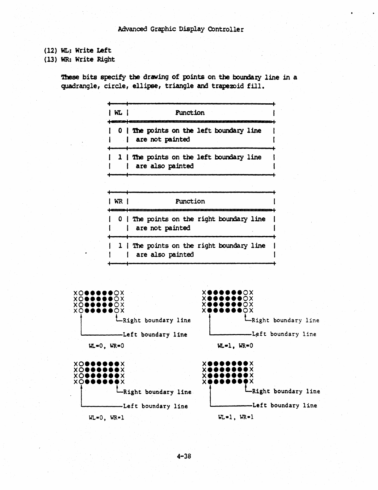
Advanced
Graphic Display Controller
(12)
WL.:
Write
Left
(13)
WR:
Write
Right
'Dlese
bits
specify
the
drawing
of
1X>1nts
on
the
boundaty
line
in
a
quadrangle,
circle,
ellipse,
triangle
and trape7X)id
fill.
I
WI.
I
Function
o I '!he
points
on
the
left
boundary
line
I
are
not
painted
1 I
1b!
plints
on
the
left
boundary
line
I
are
also
painted
I
WRI
Function
o I The
plints
on
the
right
boundary
line
I
are
not
painted
1
'l1le
points
on
the
right
boundary
line
are also
painted
xo
•••••
ox
XO
•••••
ox
XO
•••••
ox
xo
•••••
ox
t
L-Right
boundaTY
line
~Left
boundary
line
t.lI,.-O,
wa-o
xo
••••••
x
XO
••••••
X
XO
••••••
X
XO
••••••
X
t .
L-Right
boundary
line
~Left
boundary
line
WL-O
t WR-l
4-38
x
••••••
ox
X
••••••
OX
X
••••••
OX
X
••••••
OX
t
L-Right
boundary
line
~L~ft boundary
line
WL-l,
WR-O
x
•••••••
x
X
•••••••
X
X
•••••••
X
X
•••••••
X
t L-R1ght boundary
line
~Left
boundary
line
WL-l t
WR-l
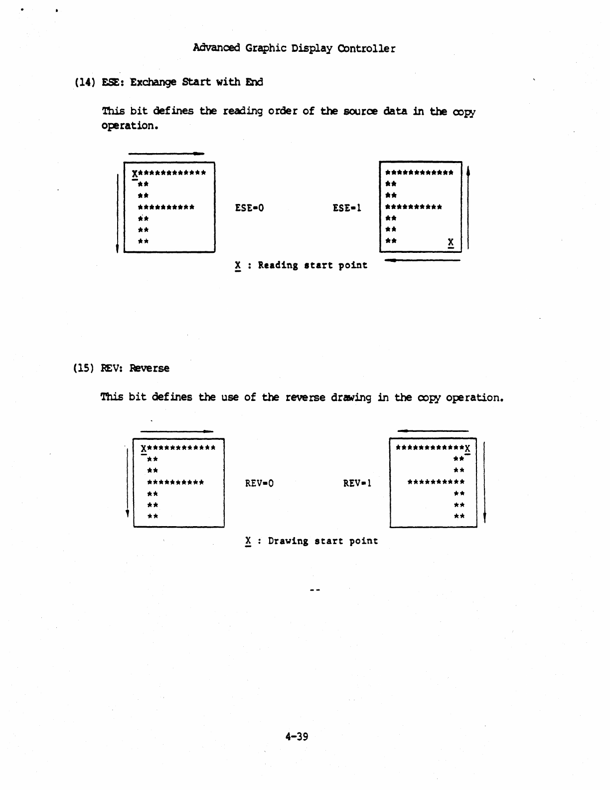
Advanced
Gr~hic
Dis~ay
Controller
(14) ESE: ExcJlange
Start
with
End
This
bit
defines
the
reading
order
of
the
source
data
in
the
oopy
operation.
•
x············
-
..
••
••••••••••
••
••
••
(15)
REV:
Reverse
ESt-O
X Reading
start
point
.***.******.
• •
• *
**
•••• * •••
*.
* •
**
•
x
This
bit
defines
the
use
of
the
reverse
drawing
in
the
ooF.i
operation
•
,
x···*****····
-
..
••
••••••••••
••
••
**
REV-O
REV-l
X Drawing
start
point
4-39
•
············X
..
-
• •
•
•••••••••
**
**
**
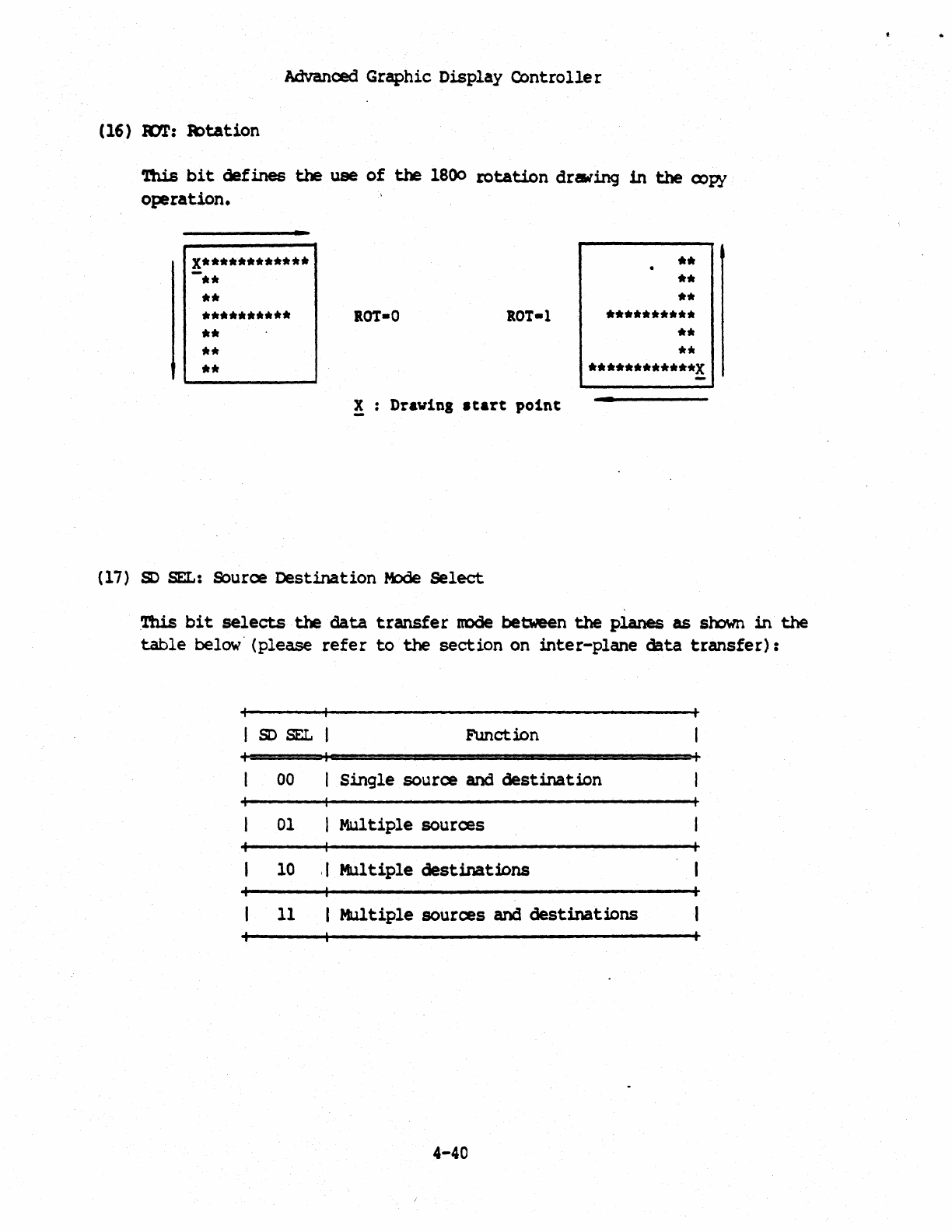
~ced
Graphic Display
Controller
(16) K7l':
It>tation
'l'his
bit
defines
the
use
of
the
1800
rotation
draring
in
the
oopy
operation.
•
x************
-.*
.*
****
•••
*
••
••
••
••
X Drawing
start
point
(17)
&>
BEL:
Source
Destination
Mode
Select
**
**
**
***.******
**
**
*******·****x
-
This
bit
selects
the
data
transfer
node between
the
planes
as
sOOwn
in
the
table
below·
(please
refer
to
the
section
on
inter-plane
data
transfer):
so
BEL
Function
00
Single
source
and
destination
01
Multiple
sources
10
,I
Multiple
destinations
11
Multiple
sources
and
destinations
4-40
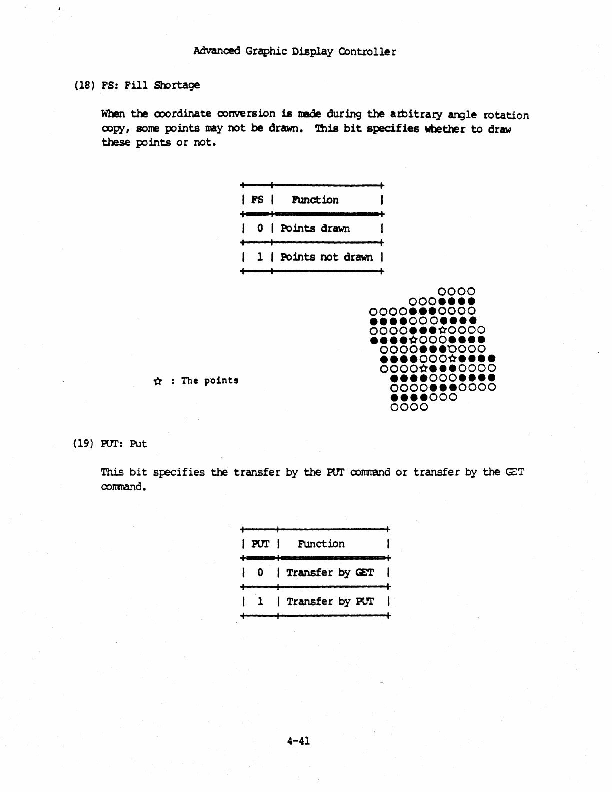
Advanced Graphic
Display
Controlle
r
(18 ) FS:
Fill
Sll:>
rtage
When
the
ex>ordinate oonversion
is
made during
the
amitraty
angle
rotation
cx>py,
some
p'ints
may
not
be
drawn.
'!bis
bit
specifies
whether
to
draw
these
p:>ints
or
not.
tt
The
points
(19)
PUT:
Put
I FS I
fUnction
o I
Points
drawn
1 I
Points
not
drawn I
0000
000
••••
0000
•••
0000
••••
000
••••
OOOO
•••
~oOOO
••••
tlOOO
••••
0000
•••
'0000
••••
ooott
••••
OOOo~
•••
OOOO
••••
000
••••
0000
•••
0000
••••
000
0000
This
bit
specifies
the
transfer
by
the
PUr
cx>mmand
or
transfer
by
the
GET
conmand.
I PUr I Function
o I
Transfer
by
CE'l'
1 Transfe r
by
PUT
4-41
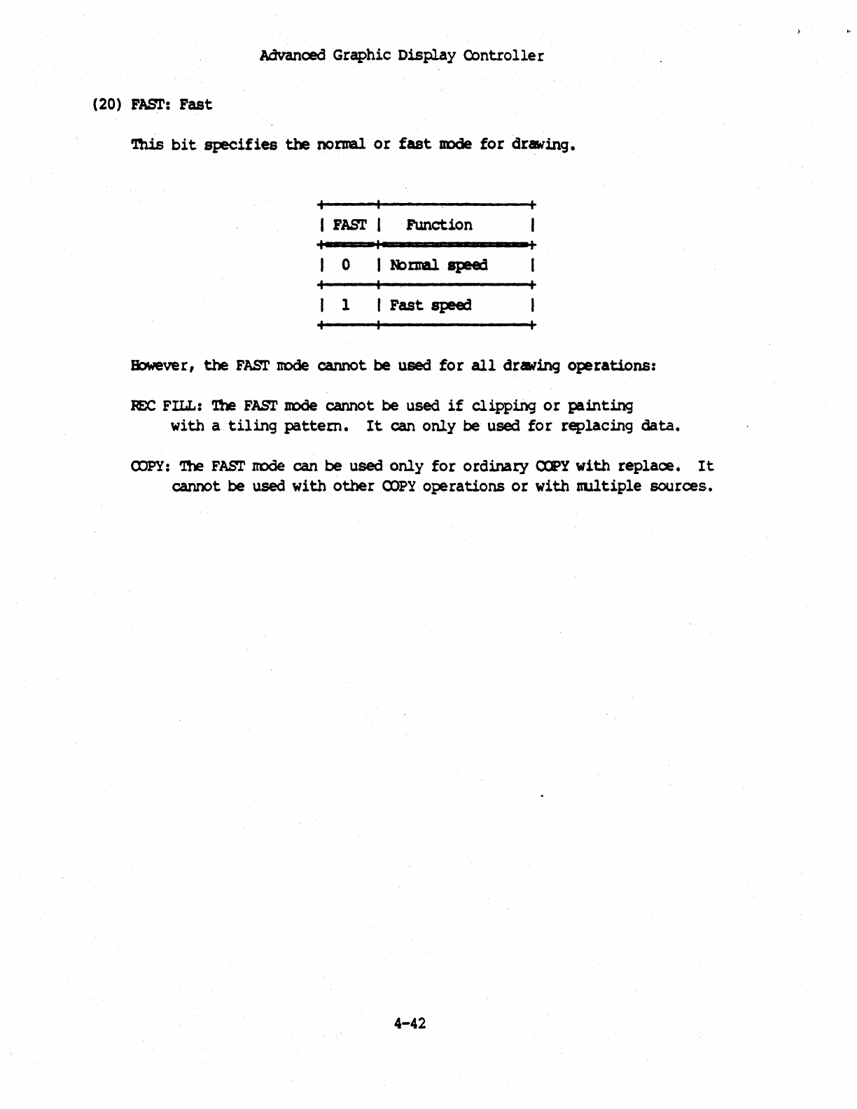
Advanced
Graphic
Display
Controller
(20)
FAST:
Fast
'lhls
bit
specifies
the
norual
or
fast
UDde
for
drawing.
I FASr I
Function
o I
R>mal
speed
1 r
Fast
speed
However,
the
FAm node cannot be used
for
all
drawing operations:
H:C
FILL:
1be
FAm
m:>de
cannot
be
used
if
clipping
or
painting
with
a
tiling
pattem.
It
can
only
be used
for
replacing
data.
COPY:
'nle
FASr
node
can
be
used
only
for
ordinaty
CXPY
with
replace.
It
cannot
be
used
with
other
<X>PY
operations
or
with
ltUltiple
sources.
4-42
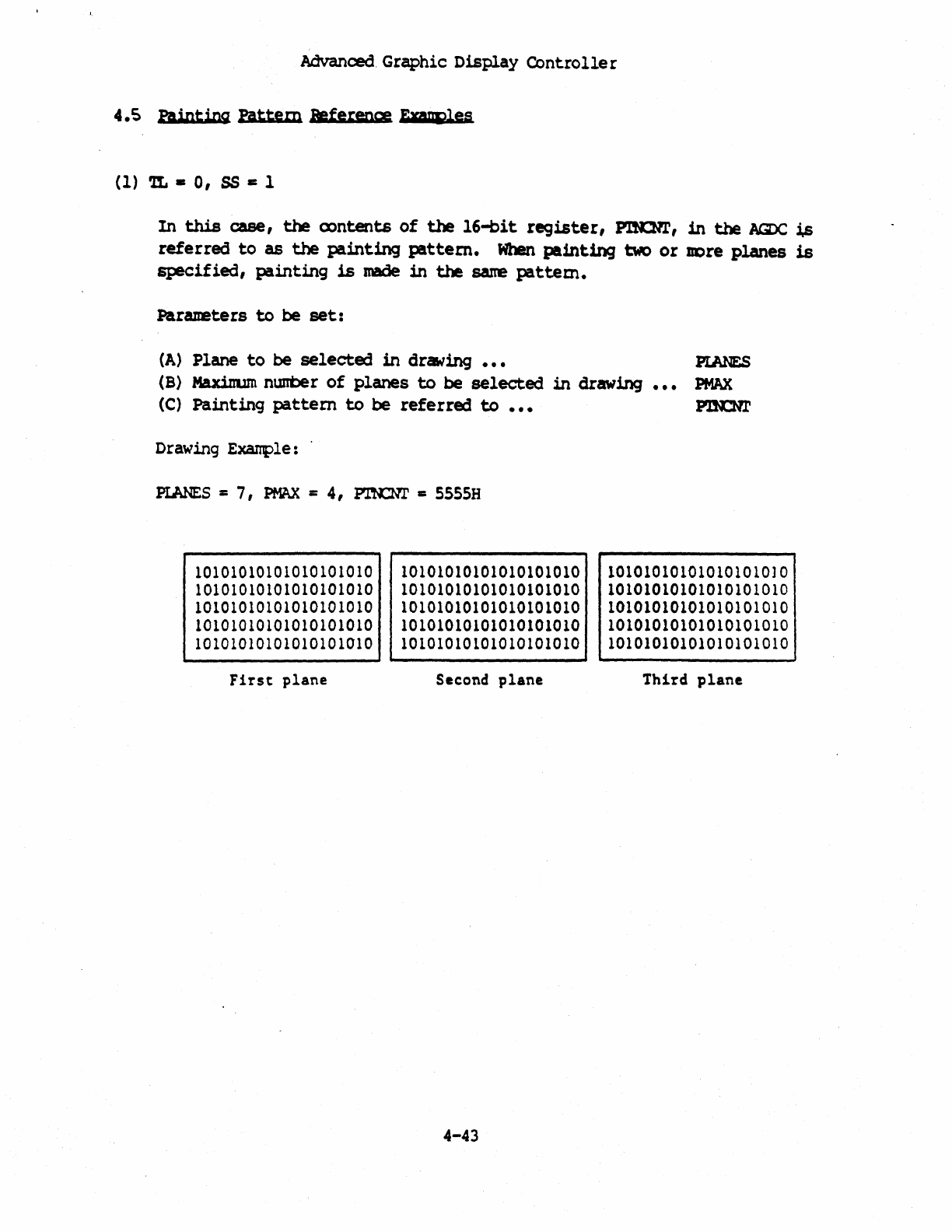
AdvanoedGraphic
Display
Controller
4.
S PAinting
Pattern
Referencz
Enpes
(1)
'1L
•
0,
SS
c 1
In
this
case,
the
oontents
of
the
16-bit
register,
1'lK:m',
in
the
AaX:,
1s
referred
to
as
the
painting
pattern.
When
painting
two
or
DDre
planes
is
specified,
painting
is
made
in
the
sane
pattem.
Parameters
to
be
set:
(A)
Plane
to
be
selected
in
drawing
•••
PLANES
(8)
Maxinum
nunber
of
planes
to
be
selected
in
drawing...
PMAX
(C)
Painting
pattern
to
be
referred
to
•••
P.LN::m'
Drawing ExaIri'le: .
PLANES
= 7,
PMAX
= 4,
PTNCNT
=
SSSSH
10101010101010101010
10101010101010101010
10101010101010101010
10101010101010101010
10101010101010101010
First
plane
10101010101010101010
10101010101010101010
10101010101010101010
10101010101010101010
10101010101010101010
Second
plane
4-43
101010101010101010]0
10101010101010101010
10101010101010101010
10101010101010101010
10101010101010101010
Third
plane
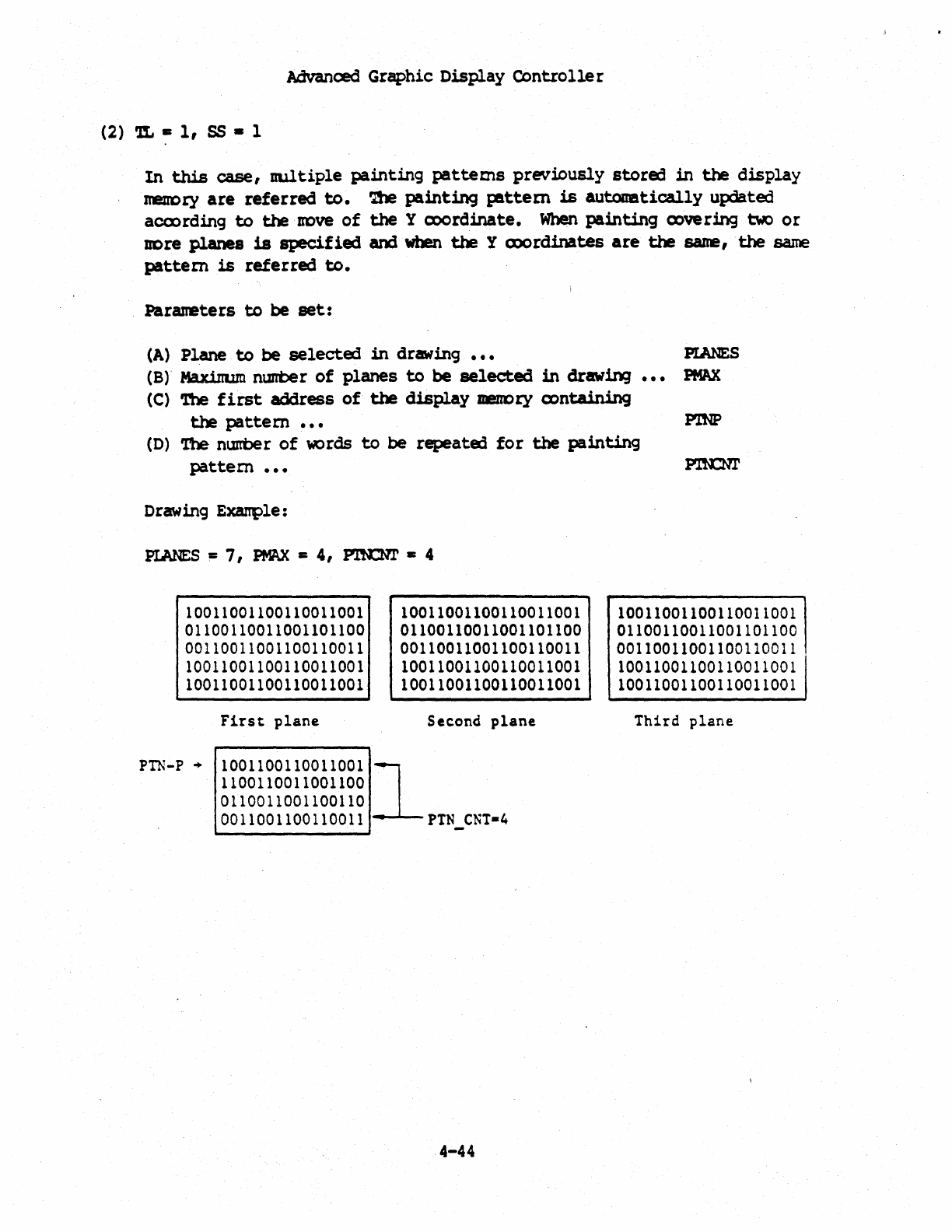
Advanced
Graphic
Display
Controller
(2)
it,
-=
1,
SS
• 1
In
this
case,
uultiple
painting
pattems
previously
stored
in
the
display
nem:>t)!
are
referred
to.
'lbe
painting
pattem
is
automatically
updated
accx>rding
to
the
rove
of
the
Y CX)()rdinate.
When
painting
mvering
two
or
IIt)re
planes
is
specified
and
when
the
Y (X)()rdinates
are
the
same,
the
same
pattern
is
referred
to.
.
Pararreters
to
be
set:
(A)
Plane
to
be
selected
in
drawing
•••
PIANES
(Sr
Maxinum nunt>er
of
planes
to
be
selected
in
drawin:J
•••
PMAX
(C)
The
first
address
of
the
display
DenOty
a>ntaining
the
pattern
•••
(D)
'Ihe nunber
of
words
to
be
repeated
for
the
painting
pattern
•••
Drawing Exanple:
10011001100110011001
01100110011001101100
00110011001100110011
10011001100110011001
10011001100110011001
First
plane
10011001100110011001
01100110011001101100
00110011001100110011
10011001100110011001
10011001100110011001
Second
plane
p~-p
..
1001100110011001 l
1100110011001100
0110011001100110
0011001100110011
PTN
CNT-4
4-44
10011001100110011001
01100110011001101100
00110011001100110011
10011001100110011001
10011001100110011001
Third
plane
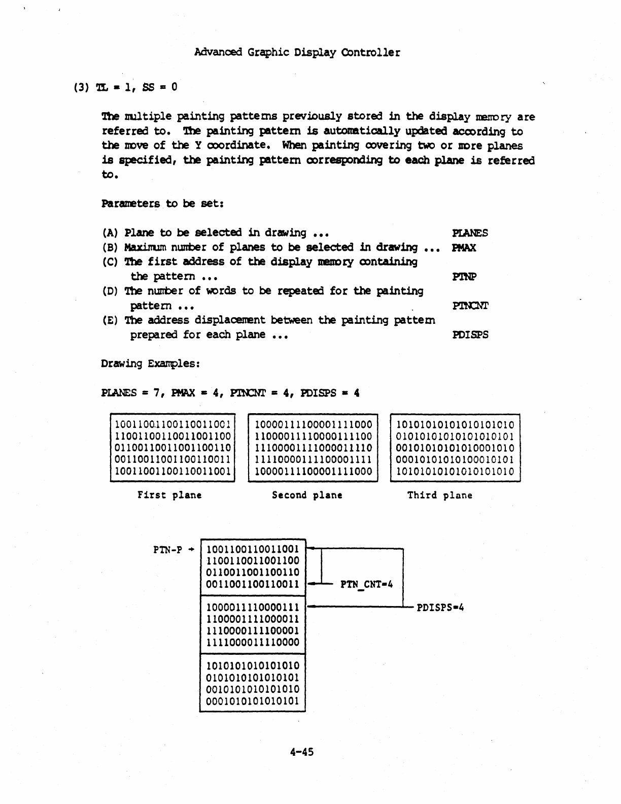
Advanced Graphic
Dis~ay
Controller
(3)
~
•
1,
SS
= 0
~
nultiple
painting
pattems
previously
stored
in
the
display
IteII'Ory
are
referred
to.
'!be
painting
pattem
is
automltically
updated acmrd1ng
to
the
DDve
of
the
Y CX)()rdinate.
When
painting
oovering
two
or
DOre
planes
is
specified,
the
painting
pattem
oorresponding
to
each
plane
is
referred
to.
Parameters
to
be
set:
(A)
Plane
to
be
selected
in
drawing...
PIANES
(B)
Maxinum
nunber
of
planes
to
be
selected
in
drawing
•••
PMAX
(C)
i!le
first
address
of
the
display
1tImDty oontaining
the
pattern...
PlNP
(D) '!be
nurrt>er
of
words
to
be repeated
for
the
painting
pattern...
PIN:Nr
(E)
'!be address
displacenent
between
the
painting
pattem
prepared
for
each plane
•••
PDISPS
Drawing
Exanples:
PLANES
=
7,
PK\X
I:
4,
PIN:Nr
=
4,
PDISPS
• 4
l00110QI100110011001
11001100110011001100
01100110011001100110
00110011001100110011
10011001100110011001
10000111100001111000
11000011110000111100
11100001111000011110
11110000111100001111
10000111100001111000
First
plane
Second
plane
PTN-P
+ 1001100110011001
1100110011001100
0110011001100110
0011001100110011
I~.......
PTN
CNT-4
-
1000011110000111
1100001111000011
1110000111100001
1111000011110000
1010101010101010
0101010101010101
0010101010101010
0001010101010101
4-45
10101010101010101010
01010101010101010101
00101010101010001010
00010101010100010101
10101010101010101010
Third
plane
PDISPS-4
Advanced Graphic
Display
OJntrolle
r
4.6
Inter-plane
DAtA
Transfers
Up
to
16
plan
••
transferrable
continuously
r---
.
r16
kinds
of
logical
opera-
tion
by
MODO.
~I
.0
f o
Source
L16
kinds
of
logical
opera-
tion
by
MODO
and
MODI.
Destination
Source
~
•
L----
16
kinds
of
logical
opera-
tion
by
MODI.
Destination
(1)
Single
Source
and
Destination
(2)
Multiple
Source
Up
to
16
planes
Up
to
16
planes
transferrable
transferrable
continuously
continuousl
1 1
~
,,----,""""'--
01
'-------'
1 0
Source
,0
litO
L 16
kinds
of
logical
opera-
tion
by
MODO
and
MODI.
Destination
Source
1...
16
kinds
of
logical
opera-
tion
by
MODO
and
MODI.
Destination
(3)
Multiple
Destination
(4)
Multiple
Source
and
Destination
4-46
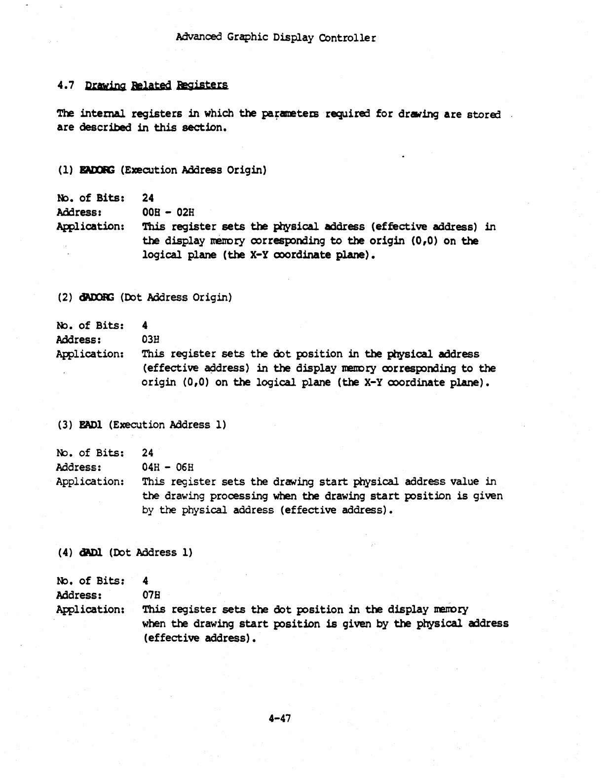
Advanced
Graphic
Dis~ay
Controller
4.7
Drawing
Belated
Begiste
rs
'!'he
internal
registers
in
which
the
pa~ametetB
requi~
for
drawing
are
storEd
.
are
described
in
this
section.
(1)
&\l'XlIG
(Execution
Address
Origin)
~.
of
Bits:
24
Address:
OOB
-
02H
Application:
This
register
sets
the
physical
address
(effective
address)
in
the
display
nenory
oorresponding
to
the
origin
(0,0)
on
the
logical
plane
(the
X-Y CX)()rdinate
plane).
(2)
CWllIC
(Ibt
Address
Origin)
N:>.
of
Bits:
Address:
4
03H
AWlication:
This
register
sets
the
oot
~sition
in
the
physical
address
(effective
a¢idress)
in
the
display
nem:>ry
oorresJ:X)nding
to
the
origin
(0,0)
on
the
logical
plane
(the
X-Y
coordinate
plane).
(3)
BADl
(Execution Address 1)
~.
of
Bits:
24
Address:
04H
-
06H
Application:
This
register
sets
the
drawing
start
physical
address
value
in
the
drawing
processing
when
the
drawing
start
position
is
given
by
the
physical
address
(effective
address).
(4)
cWll
(Ibt
Address
1)
N::).
of
Bits:
4
Address:
078
Application:
This
register
sets
the
dot
position
in
the
display
BeIIDty
when
the
drawing
start
position
18
given
by
the
plTjsical
address
(effective
address).
4-47
Advanced Graphic
Display
Controller
(5)
BADZ
(Execution Address
2)
!i).
of
Bits:
24
Address:
OSB
-
OAB
Application:
This
register
sets
the
drawing
start
physical
address
in
the
drawing
processor
when
the
drawing
start
~sition
is
given
by
the
physical
address
(effective
address).
(6)
dMJ2
(D:>t Address 2)
R:>.
of
Bits:
4
Address:
OBB
Application:
This
register
sets
the
dot
position
in
the
display
DeDl;)ry
when
the
drawing
start
position
is
given
by
the
physical
a:1dress
(effective
address).
(7)
PDISPS
(Plane Displaoenent Source)
N:>.
of
Bits:
Address:
Application:
24
OeB
-
OEB
This
reg
iste
r
sets
the
nlU1"be
r
of
words which OCCUP.i one
meno
ry
plane
in
the
case
of
display
nenory oonfigured
with
two
or
JIOre
planes.
In
the
case
of
execution
of
the
COpy
conmand,
the
nUl"Cber
of
words ~r source
plane
is
set.
In
the
case
of
execution
of
the
PAINr
ool1'll'IBIld,
the
nurreer
of
words
~r
plane
oontaining
the
painting
J;8ttem
(tiling
J;8ttem)
is
set.
(
8)
PDISPD
(Plane Displacerrent
Destination)
~.
of
Bits:
Address:
Application:
24
lOB -128
This
register
sets
the
nurrber
of
words
whi~
occupy one menory
plane
in
the
case
of
display
IIeIl'Ory
oonfigured
with
two
or
nore
planes.
In
the
case
of
execution
of
drawing
oomrrands,
the
niurber
of
words
per
plane
for
gralilics
drawing
is,
set.
In
the
case
of
execution
of
CDPYoonmmds,
the
nurrber
of
words
per
destination
plane
is
set.
In
the
case
of
execution
of
painting
oonrnands,
the
nunt>er
of
words
per
painting
plane
is
set.
4-48
Advanced
Graphic
Display
Controller
(9)
HLU
(Plane Maxinum)
N:>.
of
Bits:
Address:
Awlication:
16
14B
-
lSa
'lhls
register
sets
selects
the
nutrber
of
planes
(up
to
16)
in
the
display
uenc
ry
to
be drawn,
as
sOOwn
in
the
following
table:
I 0000 0000 0000 0001
I 0000 0000 0000 0010
I 0000 0000 0000 0100
I •
I •
I
I
0100
0000 0000 0000
I 1000 0000 0000 0000
I
Plane
to
be drawn
ttltil
1st
plane
J
unw 2nd
plane
I
tlltil
lrd
plane
I
• I
• I
• I
Until
15th
plane
I
Until
16th
plane
I
(10) lIDO (Drawing
Mode
0)
N:>.
of
Bits:
4
Address:
16H
Application:
This
registers
defines
the
type
of
logical
operation
perforned
during
drawing
processing.
When
the
bit
in
PIANES
oorrestx'nding
to
the
merrory
plane
is
0
during
drawing
processing,
the
logical
o~ration
defined
by
KDO
is
executed.
(11)
JD)l
(Drawing
ltxle
1)
NJ.
of
Bits:
Address:
Application:
4
16H
This
registers
defines
the
type
of
logical
operation
perfomed
during
drawing
processing.
When
the
bit
in
PLANES
cx>rresp>nding
to
the
nerroIy
plane
is
1
during
dra'Wing
processing,
the
logical
operation
defined
by
r«DO
is
executed.
4-49
Advanced Graphic
Display
COntrelle r
(12)
PJ!W
(Pattem
Pointer)
!b.
of
Bits:
24
Address:
18B
-lAB
Awlication:
This
registers
sets
the
first
Pr¥sical
address
in
the
display
ueuoty
area
Q)ntainin9
the
painting
(tiling)
plttem.
(13)
sma:
(Stack
Pointer)
~.
of
Bits:
24
Address:
·lea
-lEB
~ication:
1bis
registers
sets
the
fitst
P"zysical
address
in
the
display
nenory
area
to
save
data
such
as
ax>minates,
etc.,
during
the
retrieval
of
the
boundary
lX)int
in
the
atbitrary
enclosed
area
painting.
It
may
be
mnsidered
as
the
working
area
of
the
ACDC
in
the
execution
of
the
PAmI'
CX)nmmd.
(14)
X,
Y,
Ill,
DY,
IS,
!S,
D,
D,
Je,
!C,
DB,
DV
~.
of
Bits:
Address:
Application:
16
each
40H
-57H,
respectively
This
is
the
group
of
registez:s used
to
set
the
paranetem
required
for
the
execution
of
various
drawing cxmnands.
8::>weve
r,
the
DX
registe
rs
is
also
used
as
the
data
p:>rt
to
output
data
read
by
the
ArD:
during
execution
of
the
READ
CDL
oomtand.
(15)
PI'lCBS
(Pitch
Source)
~.
of
Bits:
Address:
~ication:
16
S8H
-
59B
This
register
sets
the
nurrber
of
addresses
in
the
horizontal.
direction
of
the
source
plane
in
the
display
JIelIDty
during
execution.
of
the
ropy
CX)mmand.
4-50
Advanced
Graphic
Display
Controller
(16 ) PI"1tBJ (Pi.tch
Destination)
R:>.
of
Bits:
Address:
Application:
16
5AB
-
SBB
'Ibis
registers
set
the
n\lli)er
of
addresses
in
the
mrimntal
direction
of
the
drawing
plane
in
the
display
DenDry
during
execution
of
paint
cxmIl1lI1ds.
(17)
~
(Store
Maxinum)
R,).
of
Bits:
Address:
AWlication:
16
SCE
-
SDH
This
register
set
the
size
of
the
display
DeDDty
area
used
to
save
data
such
as
(X)()rdinates,
etc.,
during
retrieval
of
the
boundary
point
in
the
atbitraty
enclosed
area
painting.
It
may
be
(X)nsidered
as
the
working
area
size
of
the
JaY:,
during
execution
of
the
PAINr
(X)mnand.
(18)
PlA!BS (Plane
Select)
No.
of
Bits:
Address:
Application:
16
SEH
-
5FH
This
register
selects
the
type
of
logical
operation
in
the
drawing
processing.
Each
bit
in
the
PIANES
registers
directly
corresp:>nds
to
a
plane.
For
the
plane
in
which
the
logical
operation
defined
by
register
KDO
is
to
be
executed,
the
corresp:>nding
bit
in
PlANES
nust
be
o.
For
the
plane
in
which
the
logical
operation
defined
by
register
l«Dl
is
to
be
executed,
the
corresp:>ming
bit
in
PII\NES
nust
be
1.
4-51
Advanced Graphic
Display
Contrelle
r
(19)
PJK:Hl'
(Pattern
CoWlt)
!t>.
of
Bits:
16
Address:
60B
-
61B
Application:
'Ibis
register
is
set
in
the
two
ways
listed
below
acau:aing
to
the
painting
pattern
in
the
execution
of
the
painting
ocmnand:
1.
In
the
case
of
painting
by
using
the
painting
pattem
previously
generated
in
the
display
DmDty
('lL
•
1),
the
range
of
words from
the
address
specified
by
the
register
PlNP
to
be
referred
to
as
the
painting
plttem
is
defined
by
the
nUDber
of
words.
2.
When
the
16-bit
data
in
the
register
Pl!CNl'
is
used
as
the
painting
pattern
(TL
•
0),
the
actual
painting
plttem
is
defined.
(20)
Ja"IN,
lCUIIH,
mlPaX,
~
(X/Y Clipping
Minim.mv'MaxiDum)
R:>.
of
Bits:
Address:
Application:
16
each
62H
-69B,
res~ctively
These
registers
define
the
rectangular
clipping
area
to
be
referred
to
during
the
drawing
processing.
XCIJUN
Clipping
Area
- - -
YCllt1AX
- - - Yru1IN
XCllt1AX
4-52
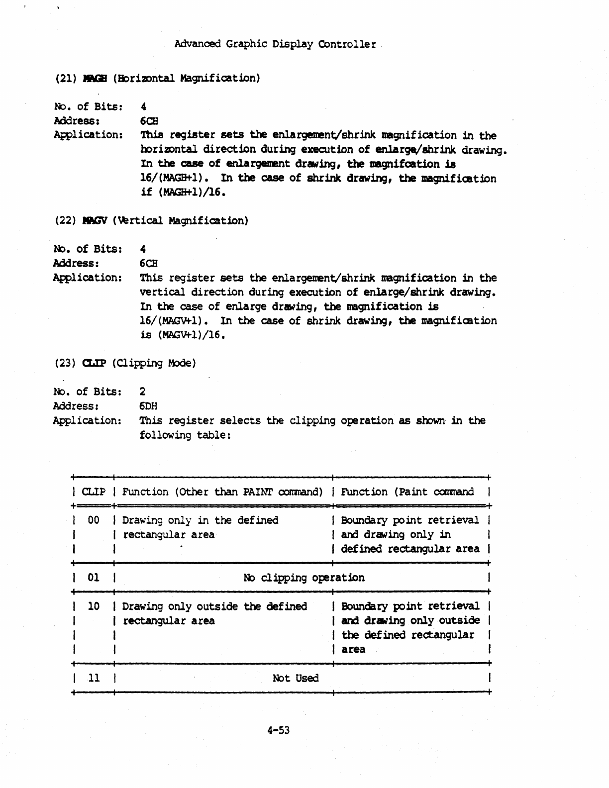
Advanced
Gr~hic
Display
Controller
(21)
IWII
(It>ri2Dntal
Magnification)
1'«:>.
of
Bits:
Address:
Application:
4
6CB
'Ibis
register
sets
the
enl.argenent/shrink
magnification
in
the
b:>ri2Dntal
direction
during
execution
of
enlarge/shrink
drawing.
In
the
case
of
enlargeuent
drawing, the magn1fcation
is
16/(MAGB+l).
In
the
case
of
shrink
drawing,
the
magnification
if
(MAGH+l)/16.
(22)
I.WN
(~rtical
Magnification)
No.
of
Bits:
Address:
Application:
4
6CB
This
register
sets
the
enlargenent/shrink
magnification
in
the
vertical
direction
during
execution
of
enlarge/shrink
drawing.
In
the
case
of
enlarge
drawing,
the
uagnification
is
16/(MACM-l).
In
the
case
of
shrink
drawing,
the
magnification
is
(MAGW1)/16.
(23) CLIP
(Cl
ipping
M:>de)
t«>.
of
Bits:
Address:
Application:
CLIP
+ +
00
01
2
6DH
This
register
selects
the
clipping
op!
ration
as
soown
in
the
following
table:
Function
(Other
than
PAIN!' conrnand)
Function
(Paint
ccmrand
Drawing
only
in
the
def
ined
I Boundary
point
retrieval
rectangular
area
I
aOO
drawing
only
in
I
defined
rectangular
area
ftl>
clipping
o~ration
10
I Drawing
only
outside
the
defined
I Boundary
point
retrieval
I
rectangular
area
I and
draiing
only
outside
I I
the
defined
rectangular
I I
area
11
t«>t
Used
4-53
+
Advanced Graphic
Dis~ay
COntroller
(24)
FLAGS,
aJIWI)
(Flags~
~)
~.
of
Bits:
Address:
Application:
16
6EH
-6Fa
'lhis
is
the
register
used
to
write
the
coummd
to
be executed
by
the
1GX,.
It
CDnsists
of
the
o~ration
(X)de (6Fa)
arx:i
the
operation
flags
(6£8).
When
the
operation
axle
is
written
to
the
oonmand
register,
N:D:.,
begins
prooess~.
4-54
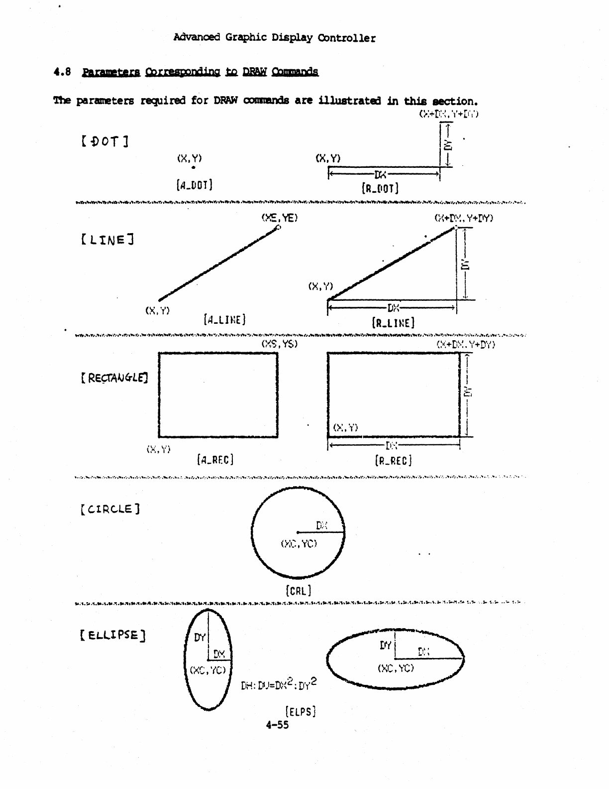
Advanced Graphic
Display
Q)ntrolle
r
The parameters
required
for
DPAW
axmands
are
illustrated
in
this
section.
(i:-!-[i:-:,
'l'+[t'I'j
[
1>
OT
]
(X,Y)
•
(A_DOT]
[LINe]
(X,
'T')
[
Re~AAJ6-LEJ
(CIRc..lE]
[ E.L.lI
PSE]
fI
<x,y)
If
t+IE---Di\-----+tl
[R_[IOT]
(~.YE)
[CRl]
'.J 2
D
!-I'
r~
I-D"'I~.
Dl'r'
t
••
L,.,,-
('
•
(ELPS)
4-55
Q
I
J
T
i
I
is
!
I
(')...
'''1
tJ
I
,....."_., _'I', ,
____
.-LL
I,j------[t:-.:-----
........
!
[Po_REC
J
(XC,
'r'C)
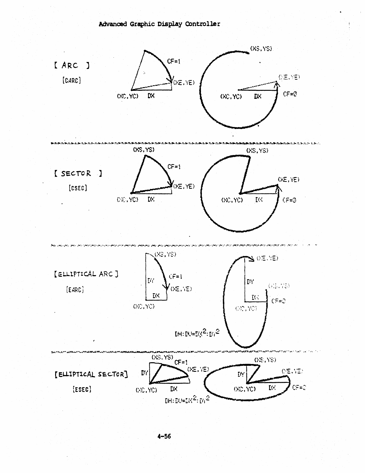
Advanced
Graphic
Display
Cantrolle
r
[ ARC
~
'F=l
,
0'
f
.t-
••
-
~\?<~.;C)
)
[CARe]
(XC.
'rtC)
D'x
(XS,ys)
[
SEcroR)
[CSEC)
;
()tE,
'iE)
c·:(:.
'r'C)
r eu-1PTlcAL ARC]
[EHRC]
DX
c:-·;C,
'r'C)
2
Ij
[
oU.
T"II
I=r("
. r,'
...
'"
J~.Lr'
....
,;.
.j.,tt
[eLLIPTIc.Al
scc...To~1
D'([:S)XE'
'tEl
[ESEC]
<:~:c
,
YC)
DX
.....
f
,_~"",,.2.
-t.·2
DH.
l.",,'-J.,.'t\ •
II
\
4-56
.......
-..-
(XS,
\'$)
(XC,yc)
DX
CF=0
GvS.
'y'S)
~\;···!::··"=··t
~
,
~
.,
....
_.
''-'
, ;
~.
f
IDY
;
......
.
4rl
:,.;
.
.:
..
,.:
..
:
if.'
.
-'
\ CF=J
• I
.,......
'.'.-
....
'
..
t":'.
J
il
.•.
:
I
(
.-
'-'.
W':-
=.;.
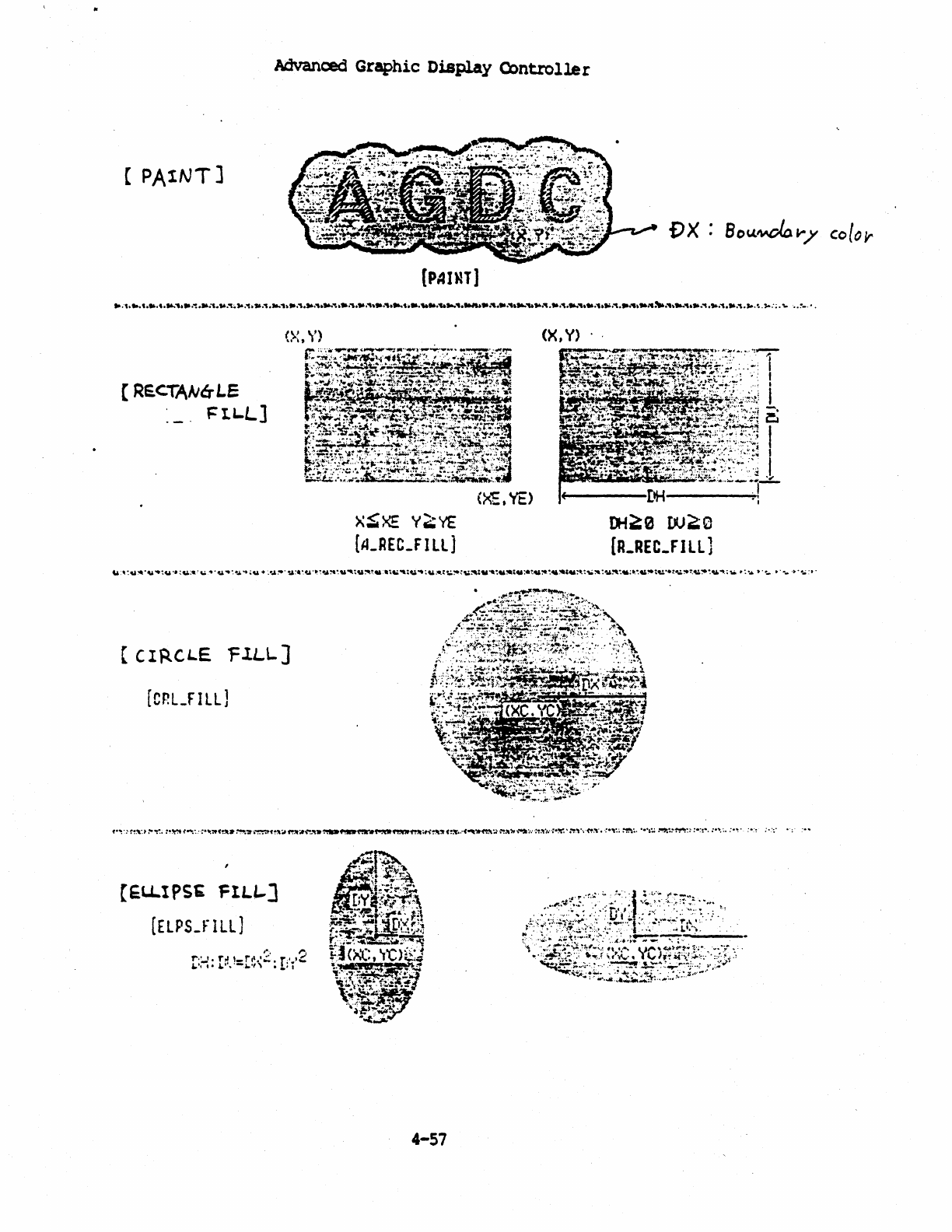
Advanced
Graphic
Display
Controlle
r
(
PAINT]
[
REC,TAAllrLE
~lL.L]
(CIRCLE
f~LL]
(EU-IPS;:
rILL..]
[ElPS_fILl]
(PAINT]
X~XE
y~YE
[ILREC_F
I
II
J
<x'E.
'fE)
(X,
y)
..
DX
.
Bou.~",,)'
co(o.,.
J)i~0
W~C
[R_REC_FIll)
;'.~;:;';;~"1t·~"fI!'.]~·!:,'''''''~:~.-.i:~;~i~~f~}'.
i~t~~
4-57
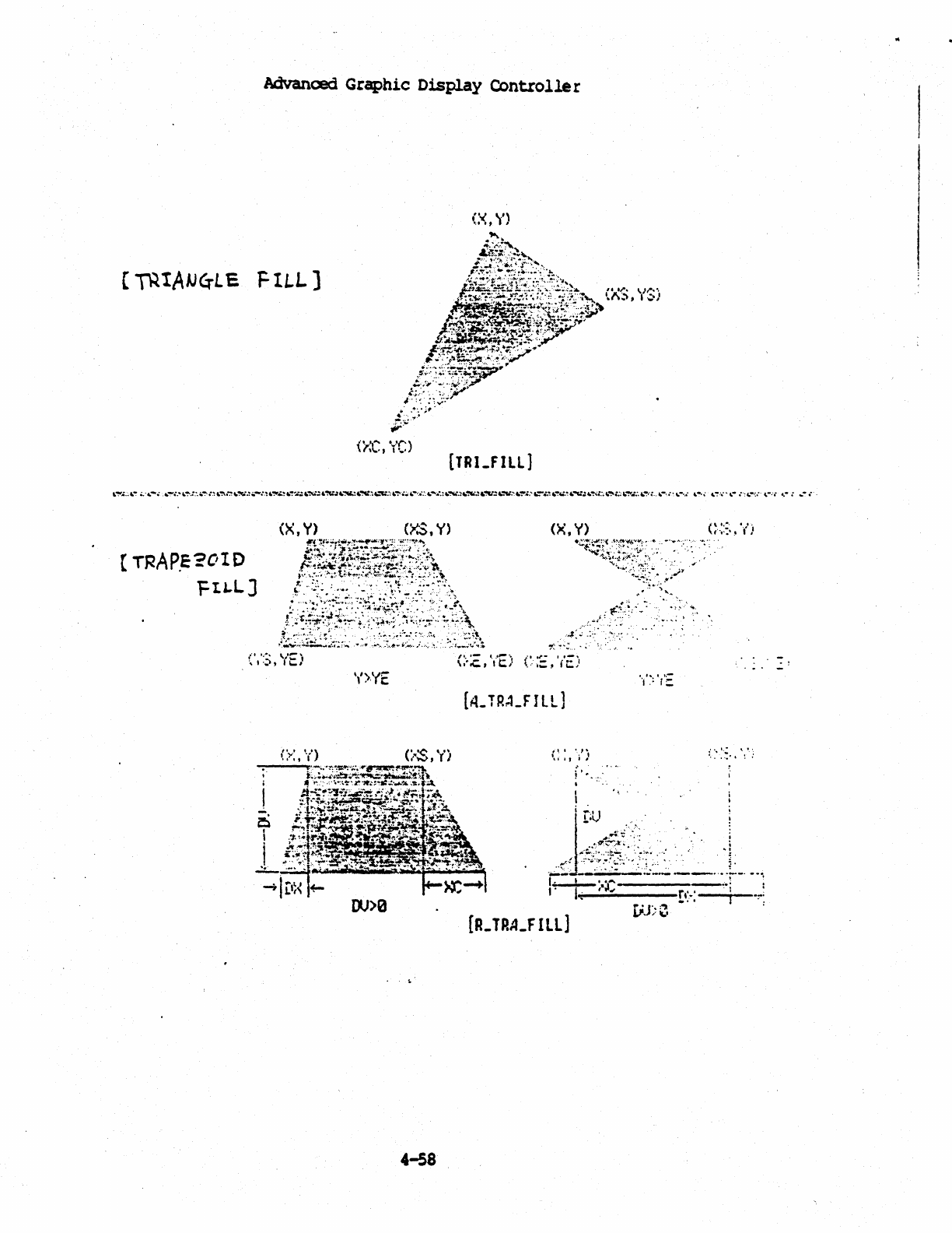
Advanced
Graphic
Display
Controlle
r
(
~
IAIJ4-L
E
FILL]
[ TRAP.E:OID
'F
t1.L J
zS
!
(X,
y)
c,<,
\')
Iti~f.rf~~l~
(~~.
YS)
/;~·S~~"I;:+l~.~..."
l1';}fJ;~~?
.:
.•....
;#.
tJ:··
[TRI_FIllJ
("'.$,
y)
c-s,
'0
~
.
4-58
(X,Y)
,....
t"
~
.
.,
"I,
1#
.
I
I
.;
.....
"
...
J
i
[.l)
"'
~
/
.:;~~:::
..
;:.,..
-j
..-.--
--._-_
..
-.-
.---_
....
:---
.....
I~·.·I""
~·.I;
t· L ,
..
~
it:.;
j
[;J>C
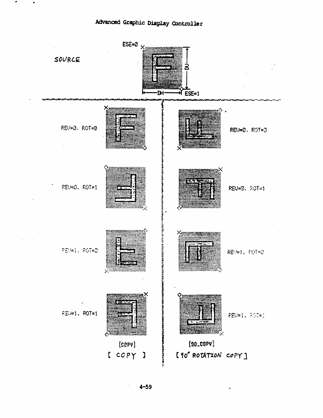
..
..
Advanced Graphic
Display
Contrelle
r
F::Ell=G.
F:OT
=9
REU=0,
ROT=l
[
[COpy]
coPY
REU=Z.
E:OT:.:1
(SO_COpy]
]
['O~
RoTATXON
COPY']
4-59
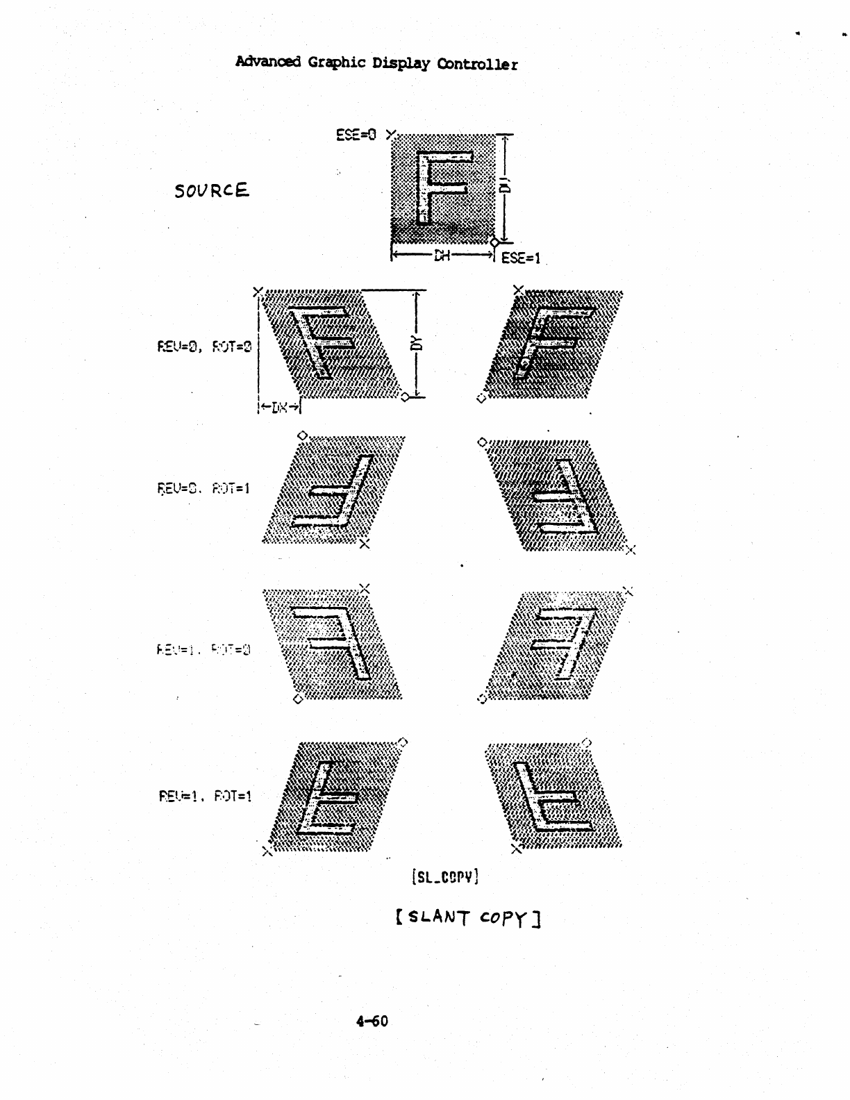
Advanced Graphic
Display
Controller
SOVRcE.
F:EU=0,
;=::)T=1
REt.i:"!.
F,',)T=1
[SLANT
copy
J
4-60
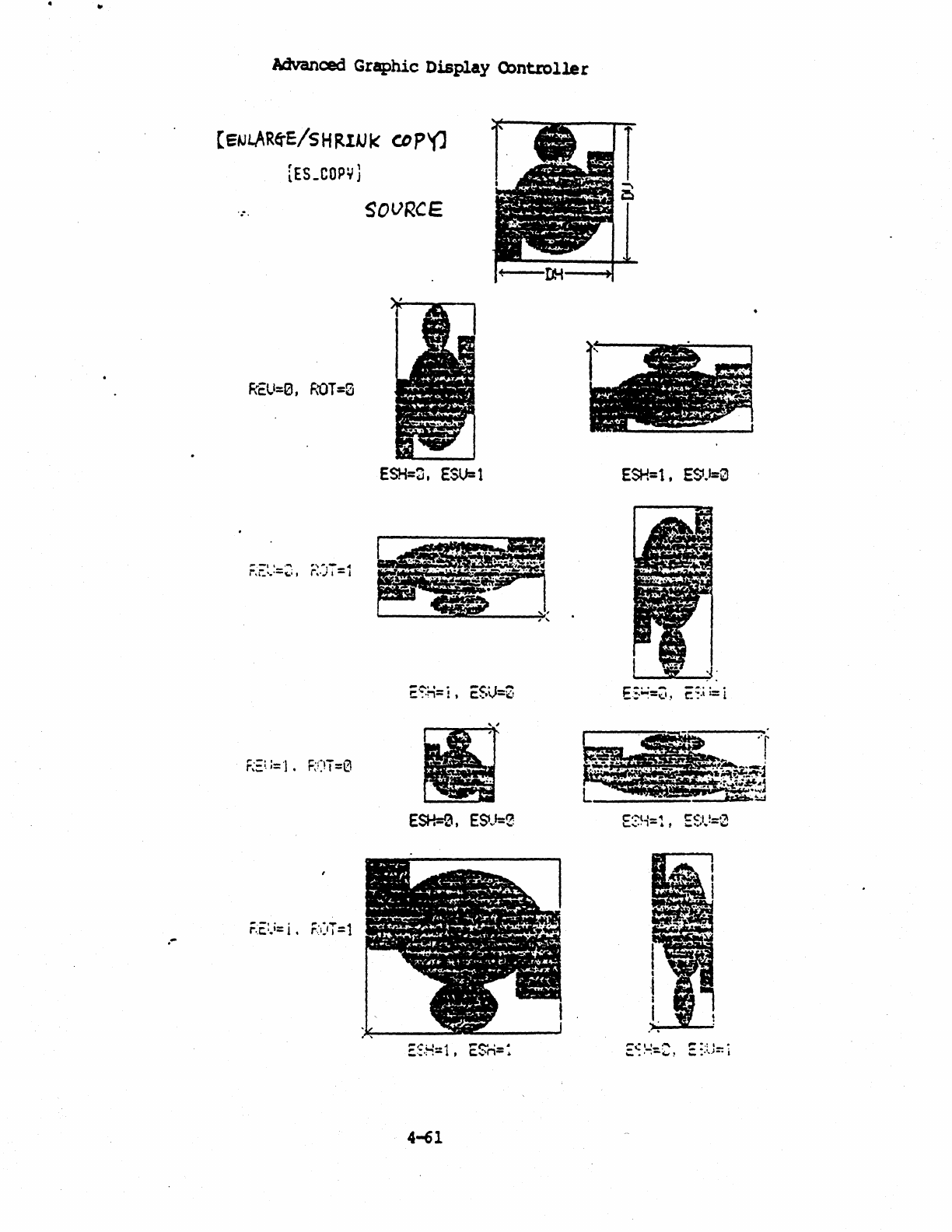
.,.
Advanced
Graphic
Display
O:>ntroller
relJL.AR~E/SHRIlJk
CDP,(]
rES_COP"]
SOVRCE
ESH=~.
ESU=
1
ESH=0,
ESIJ=2
4-61
ESH=l.
ES1.i=0
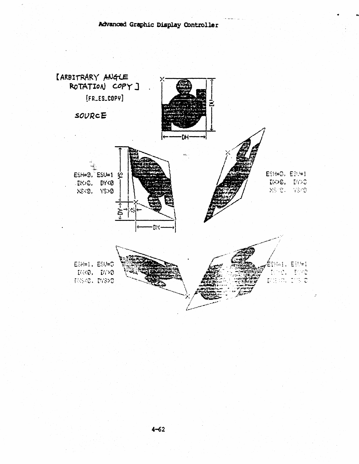
Advanced Graphic
Display
Controlle
r
[ARBIIRARY
!rfJqi..S
koTATION
ccpy
J
[FR_ES_COPY1
SOVRcE
ESH=21,-ES;U=l
-
n\t>G,
DY<0
>\s<0,
1'~S)0
4-62
..
,.
"-
:.
1;.-
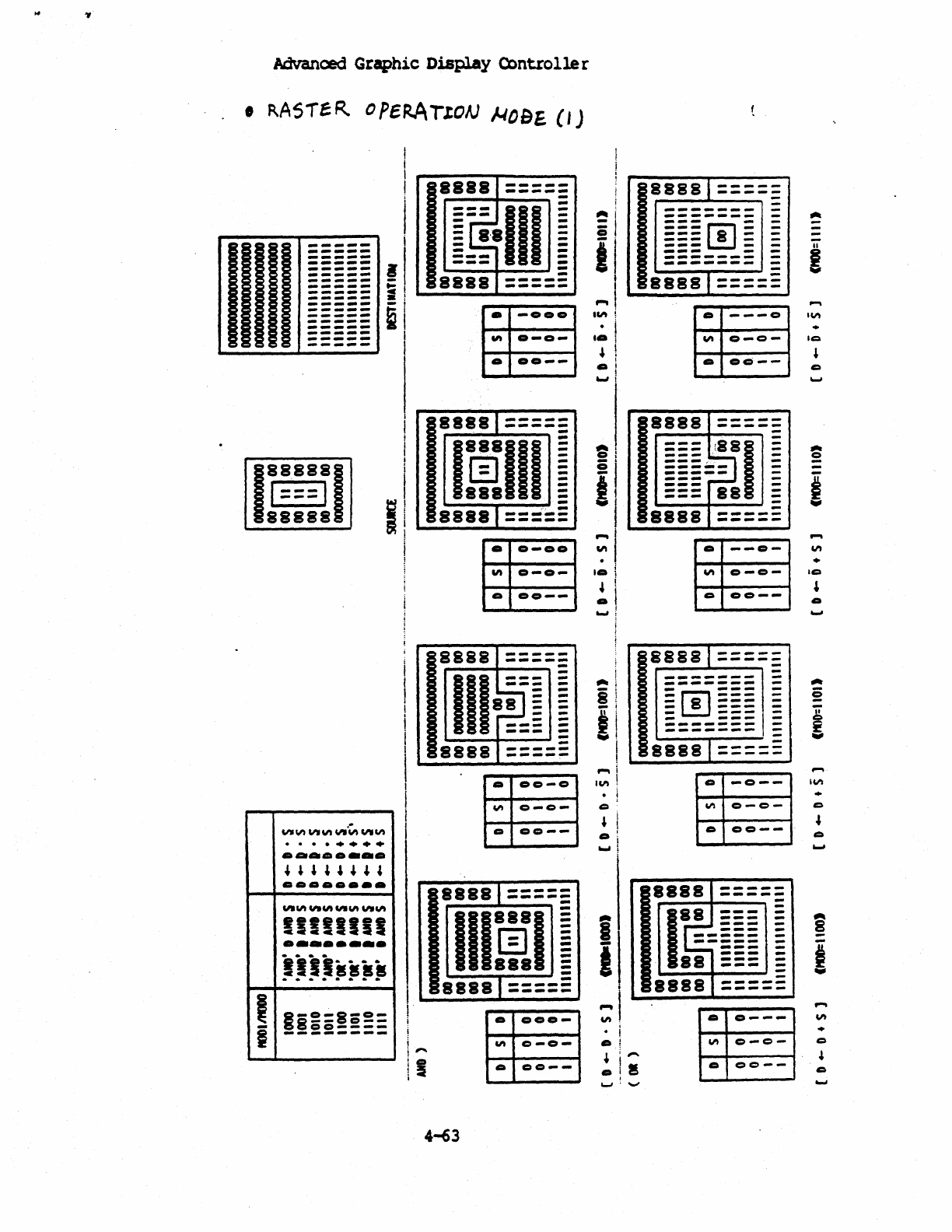
Advanced
Graphic
Display
Controlle
r
•
RAs,eR.
OPE.AATl.OIJ
).iDeE.
(I)
I
-----
-----
-----
-~---
-----
-----
-----
-----
-----
-----
-----
-----
-----
-----
-----
-----
-----
-----
I
I
I
I
i
,I
=1
al
mi
I
I
1
888881
1===1
88888
""'loll
VII,,",
w·~
"'''"'
. .
••••••
•
aUllla
• _
••
~"""~
a.a
•••••
"'''''''''''''''"'w'"''
!!I!!IIS
..
-
.....
~~-~~;;;
,
1-
0-8-0-
i
-§~§=!==
8888
-----
-----
-
-
1::
8
111
-
-
-
-
-
-
-
-
-
-
-
8888
-----
-----
•
-000
'"
0-0-
•
0.--
88881=====
Iffilll
~
8888T=====
•
0-00
'"
0-0-
•
00--
8888
-----
-----
-
-
Ills:]
-
-
-
-
-
-
-
-
-
-
-
-
8888
-----
-----
•
00-0
'"
0-0-
•
00--
88881====:
Illffil
~
88881=====
•
00.-
'"
0-0-
-
! •
00--
4-63
--
-
i
....
.'"
••
••
....
.'"
i
I
88881====:
------- -
------- -
===[!]=
=
---
8 - -
---
--
---
--
---
--
------- -
-------
-
88881=====
•
---0
""'
0-0-
•
oc--
8888
-----
-----
---
'881
---
,!,
---
===-."-
-----
-
---
===
88
-
8888
-----
-----
•
--0-
'""
0-0-
•
00--
88881====:
-------
-------
--
=[!]===
=
- 8
---
-
--
....
~-
-
----
-
------
------- -
------- -
88881=====
• -0--
VI
0-0-
•
00--
8888
-----
-----
-
rs
===
-
-
---
-
-----
-
------
-
---
88
:=:
-
-
8888
-----
-----
•
0---
""'
0-0-
•
00--
ii
I
IQ
2
-
-
Vt
•
IQ
•
•
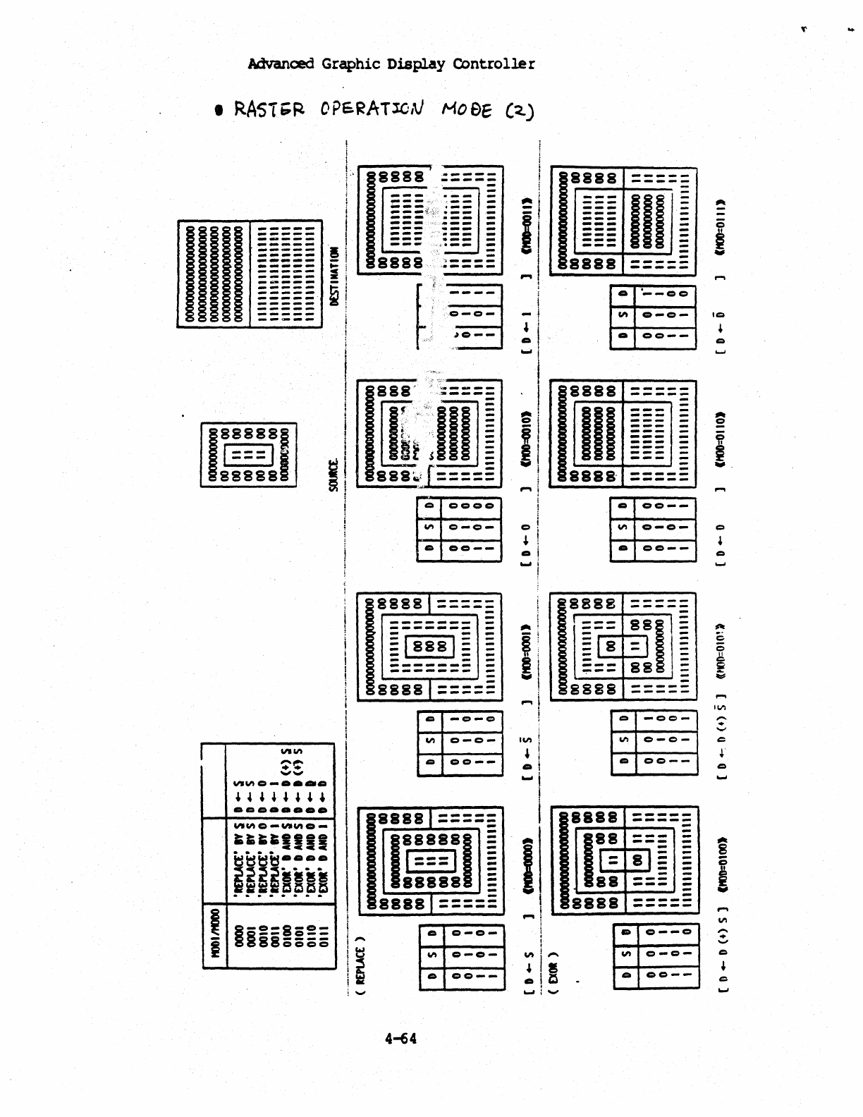
I
Advanced Graphic
Display
Cantrolle
r
•
RAS1';~
OP6.~ATlO,.J
MOSE
C<..)
I
i
-----
-----
------
_
...
---
----~
-------
.......... -
=====
-----
_
.....
_--
-----
-----
-----
-----
-----
-----
-_
...
_-
!
i
I
I:,
I
j
I
8\
-I
~!
!!i
~I
i
i
I
!
I
I
I
!
I
I
51
i
"'",.
~¢"
--
"'",.0-0_.0
4
~
,
~
, , , ,
0000_0
••
",,",,o-w,",,o-
=lD,.,.
••••
ecce
itltltl
........
:5~§
...
•
.
~~.
~~~~
1-
0-8-0-
§--
0--
88SSee
-
8888
8888
-----
-----
-
-
~-
..
--
'.----
~
....•...
••
;'~
.....
-
..
---
0-0-
;
.~o--
ti~unl
8g8~i
====:
0
0000
""
0-0-
0
00--
88881=====
-
-------
-------
-
§1
888
1§
-
-
-------
-
-------
-
-
8888l=====
0
-0-0
VI
0-0-
a
00--
88881====:
r
SS88
1 §
1===1
E
88888
E
88881=====
a
0-0-
""
0-0-
a
00--
4~4
I
o
...,
....
•
...,
I
....
...,
-
8888
-----
-----
-
-
---
III
---
---
---
---
---
-
---
---
---
-
8888
-----
-----
•
'--00
'""
0-0-
0
00--
8888
-----
-----
-
III
--- -
--- =
---
-
--- =
---
---
-
--- =
---
--- -
888a
_
...
_--
-----
0
00--
VI
0-0-
0
oc--
8888
--~--
-----
---
881
1§
---
-
§18
-I
=
;8
I~
-
--- -
8888
-------
-----
0
-oe-
VI
c-e-
0
oe--
8888
-----
-----
-
-
r8
---
--- =
-
1=
81E
-
-
-
88
---
---
-
-
-
8888
-----
-----
lID
0--0
VI
0-0-
0
cc--
IC
-
IVI
-
.
-
~.
....
VI
-
•
-
C
c
....,
,.-t<j~".""".,
'?
;7:
oj
pPD72120
..
--------------------~--------------------------------------------------------------------------------------
..
~
.......
"
-;)
\-
NEe
N\EC
Electronics
Inc.
CORPORATE
HEADQUARTERS
401
Ellis
Strllt
PO
8017241
Mountain
View.
CA
94039
TEL
415·960-6000
TWX
910·l79·698S
.,.
NEC
lleCtrOftiCllnc./Pnntad
In
U.SA
,.f
I
.'
~
•.
it'
C::':/t
..
For
Ut.,.ture
call
Toll
F,..:
1-100-832-3531
1-I00-I32·3532 (In California)
NO
pa"
Of
ttll' ooeument
may
be oopieG or r-.procIucect
in
any form or
by
any
!MIInt
witftou1
the
~"Of
wnften
COftM"\!
0'
NEe
EleCttOftiCIlne The IntormetlOl'lln Ihil ctocumentlS
~
to
Cf\ente
WIthout
nota.
EMvIClllIOICI
by
NEC
EleCtronlCl
Inc
a,.
~
by
the
..
rranty
ano
patent
InctemniftGItlOfl
ptO¥.-iOnt
appMnng
In
NEC
EIec:tronICl
Inc
Term.
ana
Concs.:
IO~
$
of
Silt
Oftly.
NEC
EiectrontcIlnc.
INk.
newarfMty
.•
~.
"Mory.
implied.
or
by
OIeCnptlon. reproins;
tnt
informatiOn
...
torltl
herein or
,.,arcsine
the tr.eoom of
...
o.crtbeCI
.,..,IC..
trom
petent
tn~t
NEC
Elec:trorliCS
Inc
ma
••
no
wartWlty
of
marct\&lltabllity or
fitneu
tor
any pyrpoee
NEC
EteCtrOfttCIlnc .
...,...
no
~Irty
for
.~)'
errora
tnat
may
appeer
in
Ihil
oocumen"
NEC
ElaCtrorttGI
Inc.
ma
••
no
commitment
to
upoate
Of
to
keep
cu".."t
tnt
intonNttOn
contll'"
1ft tnil
aocument
NECEl.(lOO85e
STOCf(NO.~
'\'
...
