Zynq UltraScale+ MPSoC Embedded Design Methodology Guide (UG1228) Ug1228 Ultrafast
User Manual:
Open the PDF directly: View PDF ![]() .
.
Page Count: 217 [warning: Documents this large are best viewed by clicking the View PDF Link!]
- Zynq UltraScale+ MPSoC Embedded Design Methodology Guide
- Revision History
- Table of Contents
- Ch. 1: Introduction
- Ch. 2: Processing System
- Ch. 3: System Software Considerations
- Ch. 4: Power Considerations
- Ch. 5: Programmable Logic
- Ch. 6: Memory
- Ch. 7: Resource Isolation and Partitioning
- Ch. 8: Security
- Ch. 9: Multimedia
- Ch. 10: Peripherals
- Appx. A: Additional Resources and Legal Notices

Zynq UltraScale+ MPSoC
Embedded Design
Methodology Guide
UG1228 (v1.0) March 31, 2017

Zynq UltraScale+ MPSoC Embedded Design Methodology Guide 3
UG1228 (v1.0) March 31, 2017 www.xilinx.com
Table of Contents
Revision History . . . . . . . . . . . . . . . . . . . . . . . . . . . . . . . . . . . . . . . . . . . . . . . . . . . . . . . . . . . . . . . . . . . . 2
Chapter 1: Introduction
Block Diagram . . . . . . . . . . . . . . . . . . . . . . . . . . . . . . . . . . . . . . . . . . . . . . . . . . . . . . . . . . . . . . . . . . . . 7
Vector Methodology . . . . . . . . . . . . . . . . . . . . . . . . . . . . . . . . . . . . . . . . . . . . . . . . . . . . . . . . . . . . . . . 9
Accessing Documentation and Training . . . . . . . . . . . . . . . . . . . . . . . . . . . . . . . . . . . . . . . . . . . . . . . 11
Chapter 2: Processing System
Defining Your Processing Needs . . . . . . . . . . . . . . . . . . . . . . . . . . . . . . . . . . . . . . . . . . . . . . . . . . . . . 13
Processing System Methodology . . . . . . . . . . . . . . . . . . . . . . . . . . . . . . . . . . . . . . . . . . . . . . . . . . . . 14
Heterogeneous Computing Concepts . . . . . . . . . . . . . . . . . . . . . . . . . . . . . . . . . . . . . . . . . . . . . . . . . 18
Application Processing Unit (APU) . . . . . . . . . . . . . . . . . . . . . . . . . . . . . . . . . . . . . . . . . . . . . . . . . . . 20
APU Virtualization Support . . . . . . . . . . . . . . . . . . . . . . . . . . . . . . . . . . . . . . . . . . . . . . . . . . . . . . . . . 23
Real-Time Processing Unit (RPU) . . . . . . . . . . . . . . . . . . . . . . . . . . . . . . . . . . . . . . . . . . . . . . . . . . . . 27
Interconnect . . . . . . . . . . . . . . . . . . . . . . . . . . . . . . . . . . . . . . . . . . . . . . . . . . . . . . . . . . . . . . . . . . . . . 29
Interrupts . . . . . . . . . . . . . . . . . . . . . . . . . . . . . . . . . . . . . . . . . . . . . . . . . . . . . . . . . . . . . . . . . . . . . . . 37
Workload Acceleration Using the PL . . . . . . . . . . . . . . . . . . . . . . . . . . . . . . . . . . . . . . . . . . . . . . . . . 42
General-Purpose Computing Acceleration. . . . . . . . . . . . . . . . . . . . . . . . . . . . . . . . . . . . . . . . . . . . . 44
Chapter 3: System Software Considerations
Defining Your System Software Needs. . . . . . . . . . . . . . . . . . . . . . . . . . . . . . . . . . . . . . . . . . . . . . . . 46
System Software Methodology. . . . . . . . . . . . . . . . . . . . . . . . . . . . . . . . . . . . . . . . . . . . . . . . . . . . . . 47
Boot Process Software. . . . . . . . . . . . . . . . . . . . . . . . . . . . . . . . . . . . . . . . . . . . . . . . . . . . . . . . . . . . . 53
System Software Stacks. . . . . . . . . . . . . . . . . . . . . . . . . . . . . . . . . . . . . . . . . . . . . . . . . . . . . . . . . . . . 58
OpenAMP Framework . . . . . . . . . . . . . . . . . . . . . . . . . . . . . . . . . . . . . . . . . . . . . . . . . . . . . . . . . . . . . 64
Xen Hypervisor . . . . . . . . . . . . . . . . . . . . . . . . . . . . . . . . . . . . . . . . . . . . . . . . . . . . . . . . . . . . . . . . . . . 67
PMU Software . . . . . . . . . . . . . . . . . . . . . . . . . . . . . . . . . . . . . . . . . . . . . . . . . . . . . . . . . . . . . . . . . . . 70
Software Development Tools . . . . . . . . . . . . . . . . . . . . . . . . . . . . . . . . . . . . . . . . . . . . . . . . . . . . . . . 72
Developer Flow . . . . . . . . . . . . . . . . . . . . . . . . . . . . . . . . . . . . . . . . . . . . . . . . . . . . . . . . . . . . . . . . . . 75
Chapter 4: Power Considerations
Defining Your Power Needs . . . . . . . . . . . . . . . . . . . . . . . . . . . . . . . . . . . . . . . . . . . . . . . . . . . . . . . . 80
Power Tuning Methodology . . . . . . . . . . . . . . . . . . . . . . . . . . . . . . . . . . . . . . . . . . . . . . . . . . . . . . . . 81

Zynq UltraScale+ MPSoC Embedded Design Methodology Guide 4
UG1228 (v1.0) March 31, 2017 www.xilinx.com
Four Major Power Domains . . . . . . . . . . . . . . . . . . . . . . . . . . . . . . . . . . . . . . . . . . . . . . . . . . . . . . . . 86
Power Islands and Power Gating . . . . . . . . . . . . . . . . . . . . . . . . . . . . . . . . . . . . . . . . . . . . . . . . . . . . 92
Platform Management Unit . . . . . . . . . . . . . . . . . . . . . . . . . . . . . . . . . . . . . . . . . . . . . . . . . . . . . . . . 93
Power Management Software Architecture . . . . . . . . . . . . . . . . . . . . . . . . . . . . . . . . . . . . . . . . . . . 95
Xilinx Power Estimator . . . . . . . . . . . . . . . . . . . . . . . . . . . . . . . . . . . . . . . . . . . . . . . . . . . . . . . . . . . . 96
Chapter 5: Programmable Logic
Defining Your PL Needs . . . . . . . . . . . . . . . . . . . . . . . . . . . . . . . . . . . . . . . . . . . . . . . . . . . . . . . . . . . . 97
PL Methodology . . . . . . . . . . . . . . . . . . . . . . . . . . . . . . . . . . . . . . . . . . . . . . . . . . . . . . . . . . . . . . . . . . 98
Logic . . . . . . . . . . . . . . . . . . . . . . . . . . . . . . . . . . . . . . . . . . . . . . . . . . . . . . . . . . . . . . . . . . . . . . . . . . 104
Integrated IP Support . . . . . . . . . . . . . . . . . . . . . . . . . . . . . . . . . . . . . . . . . . . . . . . . . . . . . . . . . . . . 108
Configuration and Partial Reconfiguration . . . . . . . . . . . . . . . . . . . . . . . . . . . . . . . . . . . . . . . . . . . 110
Power Reduction Features . . . . . . . . . . . . . . . . . . . . . . . . . . . . . . . . . . . . . . . . . . . . . . . . . . . . . . . . 111
Chapter 6: Memory
Memory Introduction . . . . . . . . . . . . . . . . . . . . . . . . . . . . . . . . . . . . . . . . . . . . . . . . . . . . . . . . . . . . 113
Defining Your Memory Needs. . . . . . . . . . . . . . . . . . . . . . . . . . . . . . . . . . . . . . . . . . . . . . . . . . . . . . 113
Memory Methodology. . . . . . . . . . . . . . . . . . . . . . . . . . . . . . . . . . . . . . . . . . . . . . . . . . . . . . . . . . . . 114
Built-In Memory Blocks . . . . . . . . . . . . . . . . . . . . . . . . . . . . . . . . . . . . . . . . . . . . . . . . . . . . . . . . . . . 116
PS DDR Memory and Controller . . . . . . . . . . . . . . . . . . . . . . . . . . . . . . . . . . . . . . . . . . . . . . . . . . . . 118
Global System Memory Map. . . . . . . . . . . . . . . . . . . . . . . . . . . . . . . . . . . . . . . . . . . . . . . . . . . . . . . 119
PS DMA Controllers . . . . . . . . . . . . . . . . . . . . . . . . . . . . . . . . . . . . . . . . . . . . . . . . . . . . . . . . . . . . . . 121
External Memory with the PL . . . . . . . . . . . . . . . . . . . . . . . . . . . . . . . . . . . . . . . . . . . . . . . . . . . . . . 125
Chapter 7: Resource Isolation and Partitioning
Defining Your Resource Isolation and Partitioning Needs . . . . . . . . . . . . . . . . . . . . . . . . . . . . . . . 127
Resource Isolation and Partitioning Methodology . . . . . . . . . . . . . . . . . . . . . . . . . . . . . . . . . . . . . 128
ARM TrustZone . . . . . . . . . . . . . . . . . . . . . . . . . . . . . . . . . . . . . . . . . . . . . . . . . . . . . . . . . . . . . . . . . 135
System Memory Management Unit . . . . . . . . . . . . . . . . . . . . . . . . . . . . . . . . . . . . . . . . . . . . . . . . . 139
Xilinx Memory Protection Unit . . . . . . . . . . . . . . . . . . . . . . . . . . . . . . . . . . . . . . . . . . . . . . . . . . . . . 142
Xilinx Peripheral Protection Unit . . . . . . . . . . . . . . . . . . . . . . . . . . . . . . . . . . . . . . . . . . . . . . . . . . . 145
Xen Hypervisor . . . . . . . . . . . . . . . . . . . . . . . . . . . . . . . . . . . . . . . . . . . . . . . . . . . . . . . . . . . . . . . . . . 149
Chapter 8: Security
Defining Your Security Needs . . . . . . . . . . . . . . . . . . . . . . . . . . . . . . . . . . . . . . . . . . . . . . . . . . . . . . 150
Security Methodology . . . . . . . . . . . . . . . . . . . . . . . . . . . . . . . . . . . . . . . . . . . . . . . . . . . . . . . . . . . . 151
Security Features Overview . . . . . . . . . . . . . . . . . . . . . . . . . . . . . . . . . . . . . . . . . . . . . . . . . . . . . . . 153
Configuration Security and Secure Boot. . . . . . . . . . . . . . . . . . . . . . . . . . . . . . . . . . . . . . . . . . . . . . 155
Device and Data Security. . . . . . . . . . . . . . . . . . . . . . . . . . . . . . . . . . . . . . . . . . . . . . . . . . . . . . . . . . 159
Protection Against DPA Attacks . . . . . . . . . . . . . . . . . . . . . . . . . . . . . . . . . . . . . . . . . . . . . . . . . . . . 162

Zynq UltraScale+ MPSoC Embedded Design Methodology Guide 5
UG1228 (v1.0) March 31, 2017 www.xilinx.com
CSU Hardware Accelerators . . . . . . . . . . . . . . . . . . . . . . . . . . . . . . . . . . . . . . . . . . . . . . . . . . . . . . . 163
Functional Safety . . . . . . . . . . . . . . . . . . . . . . . . . . . . . . . . . . . . . . . . . . . . . . . . . . . . . . . . . . . . . . . . 163
Chapter 9: Multimedia
Defining Your Multimedia Needs . . . . . . . . . . . . . . . . . . . . . . . . . . . . . . . . . . . . . . . . . . . . . . . . . . . 165
Multimedia Methodology . . . . . . . . . . . . . . . . . . . . . . . . . . . . . . . . . . . . . . . . . . . . . . . . . . . . . . . . . 166
DisplayPort . . . . . . . . . . . . . . . . . . . . . . . . . . . . . . . . . . . . . . . . . . . . . . . . . . . . . . . . . . . . . . . . . . . . . 167
GPU . . . . . . . . . . . . . . . . . . . . . . . . . . . . . . . . . . . . . . . . . . . . . . . . . . . . . . . . . . . . . . . . . . . . . . . . . . . 173
VCU . . . . . . . . . . . . . . . . . . . . . . . . . . . . . . . . . . . . . . . . . . . . . . . . . . . . . . . . . . . . . . . . . . . . . . . . . . . 181
Chapter 10: Peripherals
Defining Your Peripherals Needs . . . . . . . . . . . . . . . . . . . . . . . . . . . . . . . . . . . . . . . . . . . . . . . . . . . 187
Peripherals Methodology . . . . . . . . . . . . . . . . . . . . . . . . . . . . . . . . . . . . . . . . . . . . . . . . . . . . . . . . . 188
GPIO . . . . . . . . . . . . . . . . . . . . . . . . . . . . . . . . . . . . . . . . . . . . . . . . . . . . . . . . . . . . . . . . . . . . . . . . . . 191
I2C . . . . . . . . . . . . . . . . . . . . . . . . . . . . . . . . . . . . . . . . . . . . . . . . . . . . . . . . . . . . . . . . . . . . . . . . . . . . 194
SPI . . . . . . . . . . . . . . . . . . . . . . . . . . . . . . . . . . . . . . . . . . . . . . . . . . . . . . . . . . . . . . . . . . . . . . . . . . . . 195
UART . . . . . . . . . . . . . . . . . . . . . . . . . . . . . . . . . . . . . . . . . . . . . . . . . . . . . . . . . . . . . . . . . . . . . . . . . . 196
CAN Controller . . . . . . . . . . . . . . . . . . . . . . . . . . . . . . . . . . . . . . . . . . . . . . . . . . . . . . . . . . . . . . . . . . 197
NAND . . . . . . . . . . . . . . . . . . . . . . . . . . . . . . . . . . . . . . . . . . . . . . . . . . . . . . . . . . . . . . . . . . . . . . . . . 201
SD/SDIO/eMMC . . . . . . . . . . . . . . . . . . . . . . . . . . . . . . . . . . . . . . . . . . . . . . . . . . . . . . . . . . . . . . . . . 202
Quad-SPI . . . . . . . . . . . . . . . . . . . . . . . . . . . . . . . . . . . . . . . . . . . . . . . . . . . . . . . . . . . . . . . . . . . . . . . 203
Gigabit Ethernet Controller . . . . . . . . . . . . . . . . . . . . . . . . . . . . . . . . . . . . . . . . . . . . . . . . . . . . . . . . 206
USB . . . . . . . . . . . . . . . . . . . . . . . . . . . . . . . . . . . . . . . . . . . . . . . . . . . . . . . . . . . . . . . . . . . . . . . . . . . 209
PCI Express . . . . . . . . . . . . . . . . . . . . . . . . . . . . . . . . . . . . . . . . . . . . . . . . . . . . . . . . . . . . . . . . . . . . . 211
SATA . . . . . . . . . . . . . . . . . . . . . . . . . . . . . . . . . . . . . . . . . . . . . . . . . . . . . . . . . . . . . . . . . . . . . . . . . . 213
DisplayPort . . . . . . . . . . . . . . . . . . . . . . . . . . . . . . . . . . . . . . . . . . . . . . . . . . . . . . . . . . . . . . . . . . . . . 214
Appendix A: Additional Resources and Legal Notices
Xilinx Resources . . . . . . . . . . . . . . . . . . . . . . . . . . . . . . . . . . . . . . . . . . . . . . . . . . . . . . . . . . . . . . . . . 215
Solution Centers. . . . . . . . . . . . . . . . . . . . . . . . . . . . . . . . . . . . . . . . . . . . . . . . . . . . . . . . . . . . . . . . . 215
Documentation Navigator and Design Hubs . . . . . . . . . . . . . . . . . . . . . . . . . . . . . . . . . . . . . . . . . . 215
References . . . . . . . . . . . . . . . . . . . . . . . . . . . . . . . . . . . . . . . . . . . . . . . . . . . . . . . . . . . . . . . . . . . . . 216
Please Read: Important Legal Notices . . . . . . . . . . . . . . . . . . . . . . . . . . . . . . . . . . . . . . . . . . . . . . . 217

Zynq UltraScale+ MPSoC Embedded Design Methodology Guide 6
UG1228 (v1.0) March 31, 2017 www.xilinx.com
Chapter 1
Introduction
The Zynq® UltraScale+™ MPSoC platform offers designers the first truly all-programmable,
heterogeneous, multiprocessing system-on-chip (SoC) device. Smart systems are increasing
in complexity with applications in the automotive industry, large database deployments,
and even space exploration, pushing the requirements of each new generation of SoC to its
limits. Requirements for increased power control, real-time applications, intensive graphical
capabilities, and processing power demand a platform with maximum flexibility. The Zynq
UltraScale+ MPSoC platform provides leading edge features that modern systems
designers demand.
Built on the next-generation 16 nm FinFET process node from Taiwan Semiconductor
Manufacturing Company (TSMC), the Zynq UltraScale+ MPSoC contains a scalable 32 or
64-bit multiprocessor CPU, dedicated hardened engines for real-time graphics and video
processing, advanced high-speed peripherals, and programmable logic. The platform
delivers maximum scalability through either dual or quad-core APU devices, offloading of
critical applications like graphics and video pipelining to dedicated processing blocks, and
the ability to turn blocks on and off through efficient power domains and gated power
islands. With a wide range of interconnect options, digital signal processing (DSP) blocks,
and programmable logic choices, the Zynq UltraScale+ MPSoC has the flexibility to fit a
diverse set of user application requirements.
This guide can be viewed as a toolbox for making decisions for a user design with respect
to the UltraScale+ MPSoC feature set. Please review the recommendations and trade-offs
carefully when determining what works best for your product. This guide is organized
around the Vector Methodology (described in Vector Methodology) to provide an initial
diagrammatic view of system design requirements mapped against the Zynq UltraScale+
MPSoC primary features. The Vector Methodology does not ensure maximum use of the
capabilities of the platform, but rather provides a graphical representation of the trade-offs
and solutions a user can make when building their product on the platform. This can result
in the de-prioritization of certain platform features within the context of the overall
solution. Using the Vector Methodology allows designers to accurately target other team
members, such as Hardware Designers, Architects, and Software Engineers, to the relevant
sections of the methodology applicable to their roles.

Zynq UltraScale+ MPSoC Embedded Design Methodology Guide 7
UG1228 (v1.0) March 31, 2017 www.xilinx.com
Chapter 1: Introduction
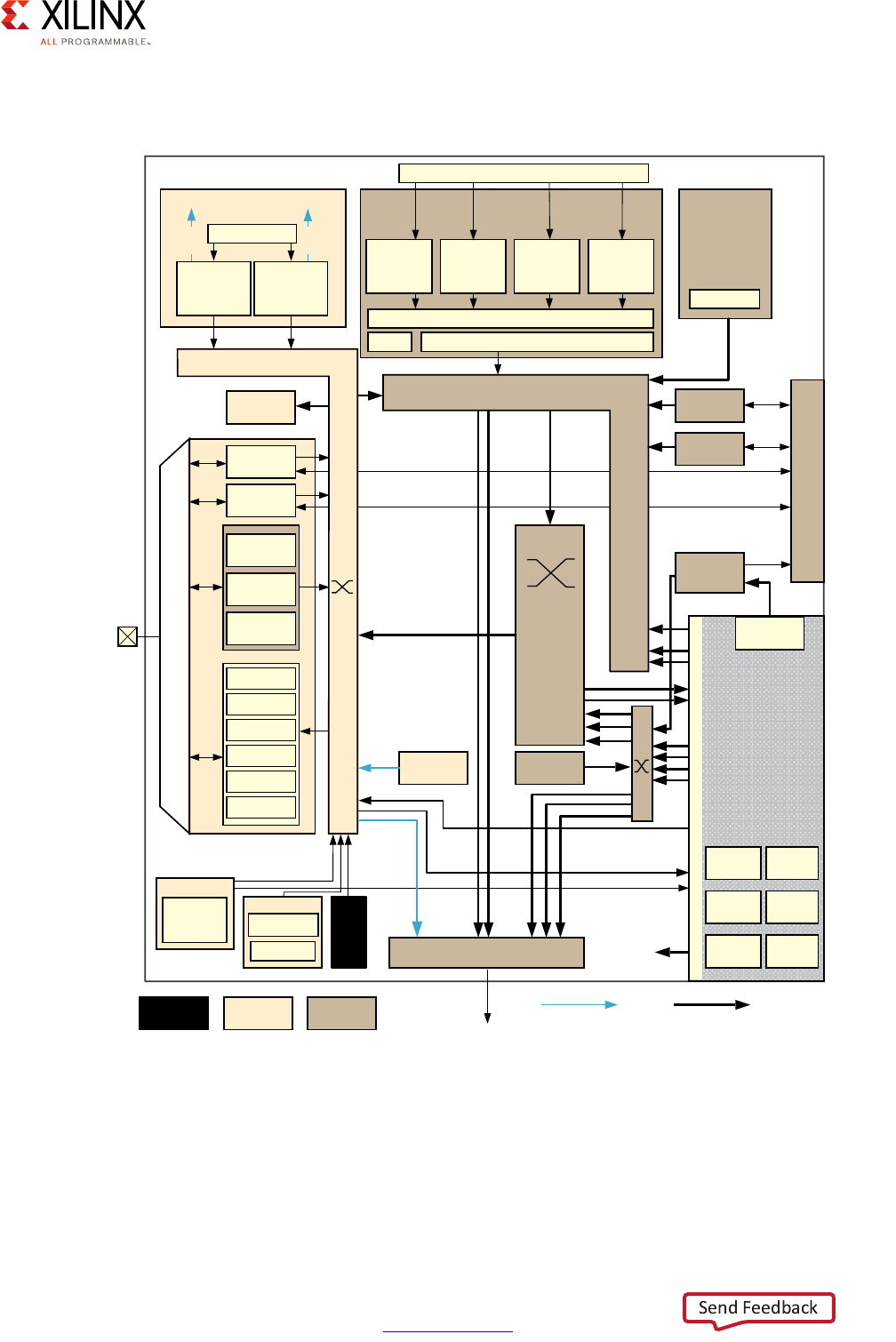
Block Diagram
A Zynq UltraScale+ MPSoC device consists of two major underlying processing system (PS)
and programmable logic (PL) blocks in two isolated power domains.
PS acts as one standalone MPSoC device and is able to boot and support all the features
shown in Figure 1-1, page 8 without powering on the PL. Each of the individual embedded
blocks are covered in this manual.
The Zynq UltraScale+ MPSoC device has four different power domains:
•Low-power domain (LPD)
• Full-power domain (FPD)
• PL power domain (PLPD)
• Battery power domain (BPD)
Each power domain can be individually isolated. The platform management unit (PMU) on
the LPD facilitates the isolation of each of the power domains. Since each power domain
can be individually isolated, functional isolation (an important aspect of safety and security
applications) is possible. Additionally, the isolation can be automatically turned on when
Zynq UltraScale+ MPSoC Embedded Design Methodology Guide 8
UG1228 (v1.0) March 31, 2017 www.xilinx.com
Chapter 1: Introduction
one of the power supplies of the corresponding power domain unintentionally powers
down.
X-Ref Target - Figure 1-1
Figure 1-1: Block Diagram
RPU
256 KB
OCM
LPD-DMA
CSU
PMU
Processing System
Cortex-R5
32 KB I/D
128 KB TCM
Cortex-R5
32 KB I/D
128 KB TCM
4 x 1GE
APU
Cortex-A53
32 KB I/D
Cortex-A53
32 KB I/D
Cortex-A53
32 KB I/D
Cortex-A53
32 KB I/D
GIC
SCU
ACP 1 MB L2
GPU
Mali-400 MP2
64 KB L2
2 x USB 3.0
NAND x8
ONFI 3.1
2 x SD3.0/
eMMC4.51
Quad-SPI
x 8
2 x SPI
2 x CAN
2 x I2C
2 x UART
GPIOs
SYSMON
MIO
Central
Switch
FPD-DMA
VCU
H.264/H.265
PCIe
Gen4
DisplayPort
v1.2 x1, x2
2 x SATA
v3.0
PCIe Gen2
x1, x2, or x4
SHA3
AES-GCM
RSA
Processor
System BPU
DDRC (DDR4/3/3L, LPDDR3/4)
Programmable
Logic
128 KB RAM
PL_LPD HP
GIC
LLLP
LLLP
RGMII
ULPI
PS-GTR
SMMU/CCI
GFC
USB 3.0
SGMII
Low Power Switch
To ACP
Low Power Full Power
Battery
Power
32-bit/64-bit
64-bit
MS
128-bit
MS
UG1085_c1_01_091715
LPD_PL HPCHPM
GTY
Quad
GTH
Quad
Interlaken 100G
Ethernet
ACE
DisplayPort
Video and
Audio Interface

Zynq UltraScale+ MPSoC Embedded Design Methodology Guide 9
UG1228 (v1.0) March 31, 2017 www.xilinx.com
Chapter 1: Introduction
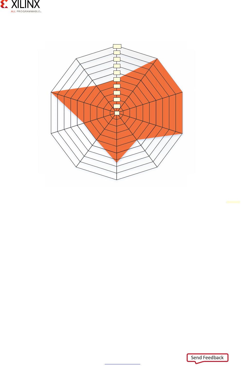
Vector Methodology
The Vector Methodology, as applied to the Zynq UltraScale+ MPSoC device, is described by
the following diagram:
In this diagram, each line radiating out from the center point represents a functional
domain of the Zynq UltraScale+ MPSoC platform. The center point represents zero
requirements/need for that functional domain, while the end of each line represents a high
level of requirements/need/complexity. Taking this diagram as a starting point, a Systems
Architect, working with a FAE or Sales Engineer, can plot the degree to which a specific
functional domain applies to their design and link those points together to get a general
sense of the problem set they are trying to address.
Consider the following Advanced Driver Assistance System (ADAS) example:
X-Ref Target - Figure 1-2
Figure 1-2: Vector Methodology Diagram
Power
Processing System
Programmable Logic
Real-Time Processing
Security
Multimedia
Memory
Peripherals
System Software
Configurations
Resource Isolation
and Partitioning
X18044-032917
Zynq UltraScale+ MPSoC Embedded Design Methodology Guide 10
UG1228 (v1.0) March 31, 2017 www.xilinx.com
Chapter 1: Introduction
In this example, we can see that the system software configurations, real-time processing,
programmable logic, and processing system are all at the maximum value. This translates
into a likely greater emphasis on specific chapters within this guide that explain the parts of
the MPSoC that a designer needs to focus on, and their pros/cons and limitations for every
one of those four vectors. With average need for power, security, multimedia, peripherals,
and resource isolation and partitioning needs, you can then appropriately scale back the
efforts to use in these areas. This allows more freedom to focus efforts on vectors that are
more critical to the product. Therefore, use of this guide allows you to translate your level
of requirements into a set of design choices and vary the degree of effort and the resources
put into optimizing certain parts of their UltraScale+ MPSoC-based designs.
Note: Although the diagram is meant as flexible tool for gauging the relevance of this guide's
different chapters, that is NOT to say that any vectors should be skipped. Be sure to read the entire
methodology guide before you make final design decisions.
X-Ref Target - Figure 1-3
Figure 1-3: Vector Methodology Example: Advanced Driver Assistance System
Power
Processing System
Programmable Logic
m
P
r
og
ra
Real-Time Processing
Security
Multimedia
Memory
Peripherals
System Software
Configurations
Resource Isolation
and Partitioning
Advanced Driver Assistance System (ADAS) Design Example
y
ste
m
P
R
e
Multimedia
l
s
re
s
Re
so
an
d
P
rocessin
g
Sy
y
Securit
y
o
ur
ce
I
so
la
ti
on
d Partitioning
y
M
emo
ry
g
70
80
90
100
60
50
40
30
20
10
0
X18043-032917

Zynq UltraScale+ MPSoC Embedded Design Methodology Guide 11
UG1228 (v1.0) March 31, 2017 www.xilinx.com
Chapter 1: Introduction
Accessing Documentation and Training
Access to the right information at the right time is critical for timely design closure and
overall design success. Reference guides, user guides, tutorials, and videos get you up to
speed as quickly as possible with Xilinx tools. This section lists some of the sources for
documentation and training.
Using the Documentation Navigator
The Xilinx Documentation Navigator ships as part of the Xilinx tools. It provides an
environment to access and manage the entire set of Xilinx software and hardware
documentation, training, and support materials. Documentation Navigator allows you to
view current and past Xilinx documentation. The documentation display can be filtered
based on release, document type, or design task. When coupled with a search capability,
you can quickly find the right information.
Documentation Navigator scans the Xilinx website to detect and provide documentation
updates. The Update Catalog feature alerts you to available updates, and gives details
about the documents that are involved. Xilinx recommends that you always update the
catalog when alerted to keep it current. You can establish and manage local documentation
catalogs with specified documents.
The Documentation Navigator has a tab called the Design Hub View. Design hubs are
collections of documentation related by design activity, such as Zynq UltraScale+ MPSoC
Design Overview, PetaLinux Tools, and the Xilinx Software Development Kit (SDK).
Documents and videos are organized in each hub in order to simplify the learning curve for
that area. Each hub contains an Embedded Processor Design section, a Design Resources
section, and a list of support resources. For new users, the Embedded Processor Design
section (shown in Figure 1-4) provides a good place to start.
Zynq UltraScale+ MPSoC Embedded Design Methodology Guide 13
UG1228 (v1.0) March 31, 2017 www.xilinx.com
Chapter 2
Processing System
The Zynq® UltraScale+™ MPSoC device gives system designers considerable power and
flexibility in the way the on-board processing capabilities can be used. In addition to the
configurability of the application processing unit (APU) and the real-time processing unit
(RPU), the Zynq UltraScale+ MPSoC device provides several dedicated processing blocks for
taking care of different types of tasks. This chapter covers the processing system
capabilities of the Zynq UltraScale+ MPSoC device, their interconnection and the
recommendations for their use.
Defining Your Processing Needs
Modern-day embedded designs often combine a complex mix of workloads, constraints
and external dependencies. Finding the best fit between each of your application's
processing needs within the many processing blocks of the Zynq UltraScale+ MPSoC device
is crucial to ensuring overall product success. The next section will start introducing you to
the core concepts behind each of the processing blocks of the Zynq UltraScale+ MPSoC
device while each block and important component will be discussed in greater detail later
in this chapter.
Meanwhile, you can start thinking about the following questions with regards to your
design:
1. What are the critical needs for your application? For each part:
a. Is it continuously processing time-sensitive data?
b. Is it real-time or mission critical?
c. Does it relate to multimedia? Or, rather, is it a general-purpose computing workload?
d. Does it require acceleration beyond the processing system's performance?
2. What type of interaction is required between system components? For each set of
components:
a. Do they need to exchange data?
b. If so, how much and at what frequency?
c. Do they need to notify each other of key events?

Zynq UltraScale+ MPSoC Embedded Design Methodology Guide 14
UG1228 (v1.0) March 31, 2017 www.xilinx.com
Chapter 2: Processing System
3. What type of interaction is required with the external world? For each part:
a. What kind of memory needs does it have?
b. Is it triggered by or does it respond to interrupts?
c. Does it need to utilize peripheral I/O?
4. Which components in your design are power sensitive?
Processing System Methodology
Given the flexibility of the Zynq UltraScale+ MPSoC device, care must be taken in
thoroughly analyzing its processing capabilities before mapping your design to any given
part. To that end, the following diagram provides a simplified view of the full system
diagram presented in this guide's introduction that highlights the main processing blocks of
the Zynq UltraScale+ MPSoC device and their interconnection through the interconnect,
with the blocks capable of conducting some form of customizable processing highlighted in
green.
Note: Figure 2-1 does NOT attempt to precisely represent the internal blocks of the Zynq
UltraScale+ MPSoC device. Instead, it is primarily a conceptual view for the purposes of the present
explanation.
X-Ref Target - Figure 2-1
Figure 2-1: Overall Processing-Capable Blocks
RPU PMU LPD
Peripherals
Inter-Processor
Communication
Framework
(OpenAMP)
APU GPU*
CSU
PL
FPD
Peripherals
Full Power Domain
Low Power Domain
Programmable Logic Power Domain
PL
Peripherals Accelerators
Accele
r
a
t
o
r
s
* GPU support is OS-specific
X18660-032917
Zynq UltraScale+ MPSoC Embedded Design Methodology Guide 15
UG1228 (v1.0) March 31, 2017 www.xilinx.com
Chapter 2: Processing System
In the following sections we will cover the various highlighted blocks in detail along with
their related interrupt capabilities, the interconnect, and the main inter processor
communication mechanism of the Zynq UltraScale+ MPSoC device. There interconnect is
made up of several different types of blocks, for instance, each warranting its own separate
discussion. For the purposes of the present explanation, we will focus on the high-level
capabilities of each part of the system.
Looking at any given type of processing need found in your design, what you can control -
as hinted to by the questions in the previous section - is:
• Processing location
• Interconnect between processing locations
• Interaction with external world:
°Memory
°Interrupts
°Peripheral I/O
In terms of processing location, there are typical candidate blocks for certain types of
workloads:
These are general guidelines and your design might call for a different approach. Another
way to help you decide on where to locate a certain processing load is to follow this
decision tree:
Table 2-1: Workload Candidates by Processing Block
Block Optimized For: Ideal For:
APU • High-level OS support such as Linux
• Hypervisor-based computing
• Symmetric Multi-Processing and Supervised
Asymmetric Multi-Processing
•HMI/UX
• Business logic
• Network/Cloud interaction
RPU • Deterministic Operation
• Low-Latency Memory Accesses
• Deterministic response time
software
• Safety-critical software
• Standards-compliant software
stack (ex: radio)
PL • Accelerating Applications • Acceleration / Parallelization
• Hardware-assisted effects,
transformations, filtering,
processing, encoding/decoding …
GPU • 2D and 3D Graphics Acceleration under Linux •Display
•Multimedia
Zynq UltraScale+ MPSoC Embedded Design Methodology Guide 16
UG1228 (v1.0) March 31, 2017 www.xilinx.com
Chapter 2: Processing System
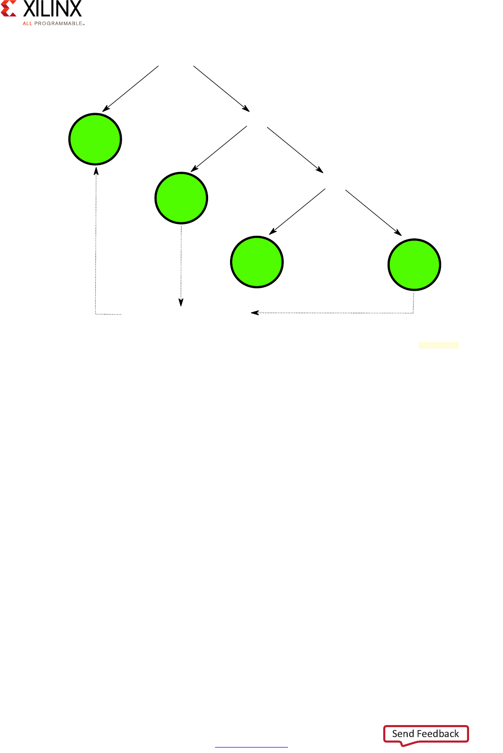
The answers to the questions in the above diagram for each of your system's components
should be fairly straight forward. If you have continuous data streams or requests that need
to be constantly processed within certain time limits, chances are the programmable logic
(PL) is the best location to put the majority of your system's components involved in
processing those data streams or requests. If a workload doesn't fit that description but still
needs to respond deterministically (i.e. in real-time) to external events or if it's mission
critical then the RPU is probably a very good candidate. If it still doesn't fit that description
then it's probably a general-purpose computing problem that should either be taken care of
by the graphics processing unit (GPU) in case of graphics or the APU for everything else.
Still, even if on a first pass you determine that certain pieces of software should be handled
by the RPU or the APU, there might be further optimization opportunities for moving those
to the PL. If, for instance, the functionality to be achieved can be described as a fixed list of
mathematical equations, such as an FFT, and/or a known set of states or state machines,
especially if they can be run in parallel, it's probably a good candidate for embedding as
part of the PL.
One way to gauge whether moving certain functionality into the PL is beneficial is obviously
manual testing and prototyping. Xilinx, however, provides you with an even more effective
way of identifying and handling optimization candidates for the PL. Indeed, the SDSoC™
and Xilinx® SDK development tools can profile your application code and, in the case of
SDSoC, enable you to offload code sections to the PL for performance testing at the click of
a button. SDSoC will automatically compile the necessary logic into the PL, assign the
X-Ref Target - Figure 2-2
Figure 2-2: Processing Location Decision Tree
Is it continuously processing time-sensitive data?
PL
Yes No
Is it real-time or mission critical?
Yes No
RPU
Is it multimedia?
Yes No
GPU* APU
Can it be optimized to PL?
Yes
* GPU support is OS-specific
X18706-032117

Zynq UltraScale+ MPSoC Embedded Design Methodology Guide 17
UG1228 (v1.0) March 31, 2017 www.xilinx.com
Chapter 2: Processing System
necessary data movers and software drivers to enable the rest of your APU- or RPU-bound
software to transparently use the accelerated software portions. SDSoC therefore helps
streamline the software acceleration process by greatly simplifying all steps involved. The
use of SDSoC vs. manual offloading is therefore a trade off between ease of implementation
and hand-crafted performance tuning.
An additional aspect to keep in mind is the top clock speeds of the processing blocks:
• APU – Up to 1.5 GHz
• RPU – Up to 600 MHz
• GPU – Up to 667 MHz
Note: Keep in mind that those are top speeds. While each block can run at a maximum at those
speeds, it's very unlikely to be running at those speeds all the time nor will it necessarily make sense
for your design.
With its ARM® Cortex®-A53 processors, the APU is the fastest general purpose computing
resource on the Zynq UltraScale+ MPSoC device. At first glance it might therefore seem to
be the best candidate for workloads requiring maximum computing power, especially since
you can have up to four Cortex-A53 processors on the Zynq UltraScale+ MPSoC device.
Maximum frequency however does not necessarily mean best fit for function. The APU's
Cortex-A53 processors, for instance, are not as well suited to real-time workloads as the
RPU's ARM® Cortex®-R5 processor. Among many other factors, there's therefore a trade
off between performance and determinism in choosing between the APU and the RPU.
Once the most likely candidate blocks for housing a given functionality have been
identified, you still need to identify the best way to move data between blocks through the
interconnect and how each processing location interacts with the various processing
resources internal to the system as well as interfaces and resources within the outside
world. The interconnect and interrupt processing are discussed in detail later in this chapter.
For all aspects related to peripheral I/O, refer to Chapter 10, Peripherals. For information
regarding the Memory, refer to Chapter 6, Memory. For more information regarding the
PL's capabilities, including its built-in accelerators, refer to Chapter 5, Programmable Logic.
Note that while the present guidelines might prescribe a given recommended processing
block, it's entirely possible that after reviewing the entire set of content related to a given
part of your design that an alternate, better-suited configuration might become evident to
best fit your specific product needs. The decision tree presented earlier, for example,
recommended using the RPU for your real-time software. Your design might, instead, call
for running a real-time operating system (RTOS) on the APU with the Cortex-R5 processors
being run bare-metal. Another example is network communications. The above
recommendations categorize network communication as being best slated for the APU. Yet,
the PL contains integrated blocks for 100G Ethernet and PCIe which, together, can be used
to efficiently accomplish network-related tasks that would typically be designated for the
APU. The Xilinx White Paper Unleash the Unparalleled Power and Flexibility of Zynq
UltraScale+ MPSoCs (WP470) [Ref 10] describes the flexibility of the Zynq UltraScale+
MPSoC outlines such an example use-case for a data center application. It also covers two
Zynq UltraScale+ MPSoC Embedded Design Methodology Guide 18
UG1228 (v1.0) March 31, 2017 www.xilinx.com
Chapter 2: Processing System
more example uses-cases, namely a central Advanced Driver Assistance System (ADAS)
module and software-defined radio (SDR), which are likely to help you get a better
understanding of how to partition your design's processing.
Yet another important aspect to keep in mind when determining where to conduct any
given part of your design's processing is power management. The architecture of the Zynq
UltraScale+ MPSoC device allows fine-grained control over power management. The power
domains illustrated in Figure 2-1, page 14 are part of this power management as is detailed
in Chapter 4, Power Considerations. Whenever you decide to run a given workload on a
given Zynq UltraScale+ MPSoC device block, keep in mind how this choice relates to your
power management needs. If, for example, a key algorithm runs on the APU and yet you
would like to have the APU be powered down during certain periods of time then you might
want to move that algorithm to either the PL or the RPU. The APU might be the most
powerful block in the system, as was explained earlier, but it also happens to be the one
that can consume the most power.
Heterogeneous Computing Concepts
Understanding the processing capabilities of the Zynq UltraScale+ MPSoC device and the
surrounding functionality calls on several key concepts not typically used outside the field
of heterogeneous computing. This is therefore a quick introduction to some terminology
you will find being used throughout this guide and the rest of the Zynq UltraScale+ MPSoC
device documentation.
The Zynq UltraScale+ MPSoC device includes two main layers of multi-processing
components (i.e. processors working in parallel to each other.) At the first layer, there are
the main processing blocks:
•APU
•RPU
•PL
•GPU
At the second layer, there are the processing units within those blocks:
• Dual or Quad Cortex-A53 cores within the APU
• Dual Cortex-R5 processor cores within the RPU
• PL-optimized applications and/or MicroBlaze™ processor instances within the PL
• Graphics processing pipelines in the GPU
The relationship between the main components of the Zynq UltraScale+ MPSoC device is
generally considered “asymmetrical.” That is, each of the APU, RPU, PL, and GPU have

Zynq UltraScale+ MPSoC Embedded Design Methodology Guide 19
UG1228 (v1.0) March 31, 2017 www.xilinx.com
Chapter 2: Processing System
different capabilities and constraints, they do not necessarily share a common OS, nor can
a workload be seamlessly moved between those blocks. Instead, designers who want to use
one of these components for a certain workload must tailor that workload specifically for
that component. This is what is called Asymmetric Multi-Processing (AMP).
Within the APU, the relationship between the Cortex-A53 processors can take four different
forms.
• If all the Cortex-A53 processor cores are used to run a single common OS such as Linux,
which is another recommended configuration, then they are said to have a
“symmetrical” relationship to one another. In this case, the common OS, Linux, can
dispatch and move workloads -- effectively OS processes -- between processors
transparently. From a software development point of view the OS API boundaries
guarantee that the software will operate just the same no matter which Cortex-A53
processor it runs on. This type of operation is known as Symmetric Multi-Processing
(SMP).
• If the Cortex-A53 processors are still operated independently, but a hypervisor such as
the open source Xen or various commercial offerings is used to coordinate their
combined operation, they would be considered as having a “supervised” asymmetrical
relationship to each other. That is, the hypervisor acts as a supervisor between the
Cortex-A53 processors and ensures there is a commonly-agreed upon arbitrator
between the independent software stacks running in parallel on the Cortex-A53
processors. Supervised AMP mode for the APU is one of the recommended
configurations in Chapter 3, System Software Considerations for certain types of
applications.
• The APU hardware should also permit a hybrid configuration. A hypervisor can be used
to segment the Cortex-A53 processors in supervised AMP mode while a subset of those
cores can be managed collectively by a single OS image in SMP mode. This however is
an advanced configuration that is neither provided nor supported by Xilinx.
• If the Cortex-A53 processors are operated independently, each running different
system software without a common OS or hypervisor between them, they too would be
considered as having an asymmetrical relationship to one another. More specifically,
they would be said to be running in “unsupervised” AMP mode, indicating that there is
no single software coordinating the operation of the Cortex-A53 processors. Note,
however, that due to the complexities of a supervised AMP configuration on the
Cortex-A53 processors, this is neither a recommended nor a Xilinx-supported
configuration for the APU, as is explained in Chapter 3, System Software
Considerations.
Finally, the APU hardware should also permit a hybrid configuration. A hypervisor can be
used to segment the Cortex-A53 processors in supervised AMP mode while a subset of
those cores can be managed collectively by a single OS image in SMP mode. This however
is an advanced configuration that is neither provided nor supported by Xilinx.
Zynq UltraScale+ MPSoC Embedded Design Methodology Guide 20
UG1228 (v1.0) March 31, 2017 www.xilinx.com
Chapter 2: Processing System
Overall, because the Zynq UltraScale+ MPSoC device combines many different types of
processors and processor cores in a single device, it is referred to as providing
“heterogeneous” computing. Being such a type of device, the Zynq UltraScale+ MPSoC
device enables the many processors and processor sets to relate to the other blocks or
processors within the same block in the various ways just described.
The following is a quick recap of the previous explanation:
• SMP: When processing cores within the APU are managed by a single OS
• AMP: When processing blocks operate independently of one another
°Supervised: When there's a hypervisor coordinating AMP blocks
°Unsupervised: When there isn't a single arbiter between AMP blocks
• Heterogeneous computing: combining different processor types in the same device
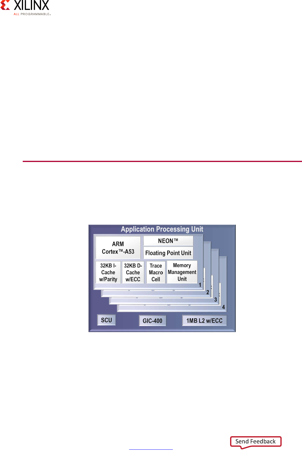
Application Processing Unit (APU)
The APU on the Zynq UltraScale+ MPSoC device includes Dual or Quad Cortex-A53
processors, depending on the specific Zynq UltraScale+ MPSoC device model you are
using.
Each of the Cortex-A53 processor cores provides, among many other features:
• ARMv8-A architecture support
• 64 or 32 bit operation
• Up to 1.5GHz performance
• Independent Memory Management Unit (MMU)
X-Ref Target - Figure 2-3
Figure 2-3: Application Processing Unit (APU) Block Diagram
Zynq UltraScale+ MPSoC Embedded Design Methodology Guide 21
UG1228 (v1.0) March 31, 2017 www.xilinx.com
Chapter 2: Processing System
• Dedicated L1 cache
• Individual power gating
• ARM TrustZone support
• VFPv4 FPU Implementation
• NEON and Crypto API support
Note: Refer to the Zynq UltraScale+ MPSoC device datasheet and Zynq UltraScale+ MPSoC Technical
Reference Manual (UG1085) [Ref 7] for the full list of features.
The Cortex-A53 processors therefore provide the same high-end general-purpose
computing capabilities required to run high-end general purpose applications and OSes as
other computing platforms as discussed in Chapter 3, System Software Considerations.
Note that while the Cortex-A53 processors are mostly independent, some of the APU's
resources, including its Global Interrupt Controller (GIC) covered below, must be managed
coherently for all Cortex-A53 processors in order for the APU to operate correctly.
Here is a more detailed view of the APU:
X-Ref Target - Figure 2-4
Figure 2-4: Detailed APU Block Diagram
APU
GIC
Cortex-A53 MPCore
Cortex-A53
FPU/NEON/Crypto
32K L1
ICache
32K L1
DCache
Debug/
Timers
Cortex-A53
FPU/NEON/Crypto
32K L1
ICache
32K L1
DCache
Debug/
Timers
Cortex-A53
FPU/NEON/Crypto
32K L1
ICache
32K L1
DCache
Debug/
Timers
Cortex-A53
FPU/NEON/Crypto
32K L1
ICache
32K L1
DCache
Debug/
Timers
Snoop Control Unit (SCU)
L2 Cache 1MB
IRQ/vIRQ
FIQ/vFIQ
Timers
Interrupts
System Counter
(in LPD) FPD Core Switch CoreSight
SPI Interrupts
64-bit counter
APB, TS
ATB
32-bit AXI
128-bit ACP
CCI
128-bit ACE
;

Zynq UltraScale+ MPSoC Embedded Design Methodology Guide 22
UG1228 (v1.0) March 31, 2017 www.xilinx.com
Chapter 2: Processing System
For more information regarding the software operation of the APU, refer to Chapter 3,
System Software Considerations and Zynq UltraScale+ MPSoC: Software Developers Guide
(UG1137) [Ref 5]. The rest of this section will focus on the APU's processing capabilities.
SMP on the APU
Xilinx provides an open source Linux that contains a kernel that is SMP aware and can be
further configured to the developer's needs. The kernel configuration allows the developer
to specify the number of CPU cores that can be used for the OS' SMP feature. Selecting a
number below the amount of available cores, and deploying with an underlying hypervisor
will keep one or more cores free for other applications such as custom bare-metal
applications created through the Xilinx SDK.
Unsupervised AMP on the APU
Unsupervised AMP on the APU implies handing control over to the first processor, which in
turn boots specific OS and runs workloads on other processors. In this working mode,
resource sharing is left for the developer to implement. As was mentioned earlier, due to
subtle complexities of implementation, this is neither a Xilinx recommended nor supported
use case of the Zynq UltraScale+ MPSoC device.
Supervised AMP on the APU
A hypervisor can be used on the APU for deploying different OSes or bare-metal workloads
on the available cores. Depending on the hypervisor itself and specific customer needs, it
can typically be used to manage resource sharing in a way that is either transparent (full
virtualization) or semi-transparent (paravirtualization) to the guests it runs. Virtualization
support is the subject of the next section.
64 or 32 Bit Operations
The Cortex-A53 processor is compatible with the ARMv8 specification which means it has
the capacity to operate in 64 bit (AArch64) and 32 bit (AArch32) execution modes. The
limitations of each mode are the same as those inherent the ARM architecture. The AArch32
execution mode on the Zynq® UltraScale+™ MPSoC is compatible with the Zynq 7000
device family and the ARMv7 specification, and has been extended to support some of
ARMv8 features like SIMD and the cryptographic extension. The choice of using either
execution mode generally depends on the software meant to run on the device.

Zynq UltraScale+ MPSoC Embedded Design Methodology Guide 23
UG1228 (v1.0) March 31, 2017 www.xilinx.com
Chapter 2: Processing System
In hypervisor mode, the choice of whether to use AArch32 and AArch64 is dictated by what
execution state is used by the hypervisor.
• A 64 bit hypervisor can run an operating system kernel running in AArch64 or AArch32
mode. Note that an OS kernel running as AArch32 can only run applications in AArch32
execution mode, even if said kernel is running within a hypervisor in AArch64 mode.
• A 32 bit hypervisor is limited to AArch32 OSes and applications.
APU Virtualization Support
The Zynq UltraScale+ MPSoC device supports hardware virtualization through 4 key
components. Several are already being used by system software designed for the Zynq
UltraScale+ MPSoC device, such as the Xen hypervisor. Understanding those capabilities
will enable you to more effectively design your system around the Zynq UltraScale+ MPSoC
device.
Cortex-A53 Processor Virtualization
Support for virtualization on the APU is typically implemented through one of the Exception
Levels (ELs) defined in the ARMv8 architecture specification of the Cortex-A53 processor.
There are 4 ELs supported by ARMv8 and EL2 can be used by supported hypervisors to
isolate the hypervisor context from the guest OSes. The Cortex-A53 processor's ELs are
discussed in detail as part of the ARM TrustZone section in Chapter 7, Resource Isolation
and Partitioning.
Zynq UltraScale+ MPSoC Embedded Design Methodology Guide 24
UG1228 (v1.0) March 31, 2017 www.xilinx.com
Chapter 2: Processing System
Interrupt Virtualization
Interrupt virtualization is discussed in APU Interrupt Virtualization, page 39.
X-Ref Target - Figure 2-5
Figure 2-5: TrustZone's Exception Levels
Non-secure State
App1
AArch64 or
AArch32(1)
App2
AArch64 or
AArch32(1)
App1
AArch64 or
AArch32(1)
App2
AArch64 or
AArch32(1)
Supervisor (Guest OS1)
AArch64 or AArch32(2)
Supervisor (Guest OS2)
AArch64 or AArch32(2)
Hypervisor Mode
AArch64 or AArch32
EL0
EL1
EL2
SVC
HVC
SMC
Secure Monitor Mode
Supervisor (Secure OS)
AArch64 or AArch32
Trusted App1
AArch64 or
AArch32(1)
Trusted App2
AArch64 or
AArch32(1)
EL3
Secure State
X15288-032917
Zynq UltraScale+ MPSoC Embedded Design Methodology Guide 25
UG1228 (v1.0) March 31, 2017 www.xilinx.com
Chapter 2: Processing System
System MMU for I/O Virtualization
The System MMU (SMMU) simplifies the virtualization of addresses for I/O and hypervisor
use by automating address translation based on software-managed tables. The following
figure illustrates one example of the SMMU's virtualization of addresses:
The SMMU can operate in two stages, as illustrated above as "S1," "S2," or "S1/S2:”
•Stage 1:
This stage operates like a traditional single-stage CPU MMU. It takes Virtual Addresses
(VAs) and translates them to Intermediate Physical Addresses (IPAs).
•Stage 2:
In a hypervisor environment, this stage simplifies the hypervisor's design by enabling
guest OSes to directly configure DMA capable devices in the system without having to
interface with the hypervisor for those requests. In this stage, it takes IPAs and converts
to Physical Addresses (PAs).
X-Ref Target - Figure 2-6
Figure 2-6: Example Use of the SMMU
Cache Coherent Interconnect
Memory
Device1 Device2
Interconnect
Device3 Device<n>
Interconnect
SMMU S2 SMMU S1/2 SMMU S1/2
CPU0 CPU1-3
MMU S1/2
L1 Cache
MMU S1/2
L1 Cache
GPU
MMU S1
Cache
Coherent Interconnect
L2 Cache
X15290-092916
Zynq UltraScale+ MPSoC Embedded Design Methodology Guide 26
UG1228 (v1.0) March 31, 2017 www.xilinx.com
Chapter 2: Processing System
The following figure illustrates the SMMU's virtualization of addresses in a hypervisor
environment:
The SMMU has the following key components that interface with the Zynq UltraScale+
MPSoC device Interconnect described in the next section:
• Translation Buffer Unit (TBU): For translating addresses
• Translation Control Unit (TCU): For controlling and managing address translation
Chapter 7, Resource Isolation and Partitioning discusses this topic further.
Peripheral Virtualization
In general, the SMMU can be used by the hypervisor to allow guests to exclusively own a
DMA-capable device. In system designs that wish to share a single hardware device across
multiple guest OSes, a technique called paravirtualization is used. This requires new device
drivers for all OSes that want to share the device. The throughput of a shared device is
accordingly less than an exclusively-owned device, as mapped by the SMMU.
X-Ref Target - Figure 2-7
Figure 2-7: SMMU Address Translation Stages
B2
A0A1
Guest OS0
B0B1
Guest OS0
Hypervisor
CPU
MMU
Memory
Accessing
Devices
System Memory
SystemMMU
B2
Guest OSm
4GB
B2
B2
0
4GB
Stoge 1 Address Translation
Under control
of Guest OS
A2
A2
Guest OSm
4GB
A2
A2
0
Stage 1 Address Translation
Intermediate Physical
Address (IPA) Space
Virtual Address
(VA) Space
4GB
B2
4GB
A2
B2
A2
Stage 2 Address Translation
Physical Address
(PA) Space
0
0
X15291-032917
Zynq UltraScale+ MPSoC Embedded Design Methodology Guide 27
UG1228 (v1.0) March 31, 2017 www.xilinx.com
Chapter 2: Processing System
Timer Virtualization
The ARM processor includes generic hardware timers for various tasks. One timer calculates
the global passing of time for the system. This generic timer is associated with a counter
incremented at a rate which depends on the system setting or the CPU frequency. Each CPU
core contains a physical counter which contains the system counter value. Each CPU core
also has a virtual counter that indicates virtual time. This virtual counter is saved and
paused when a virtual machine gets interrupted and the control returns to the hypervisor.
Access to the counter values can be controlled by the OS depending on the execution
levels.
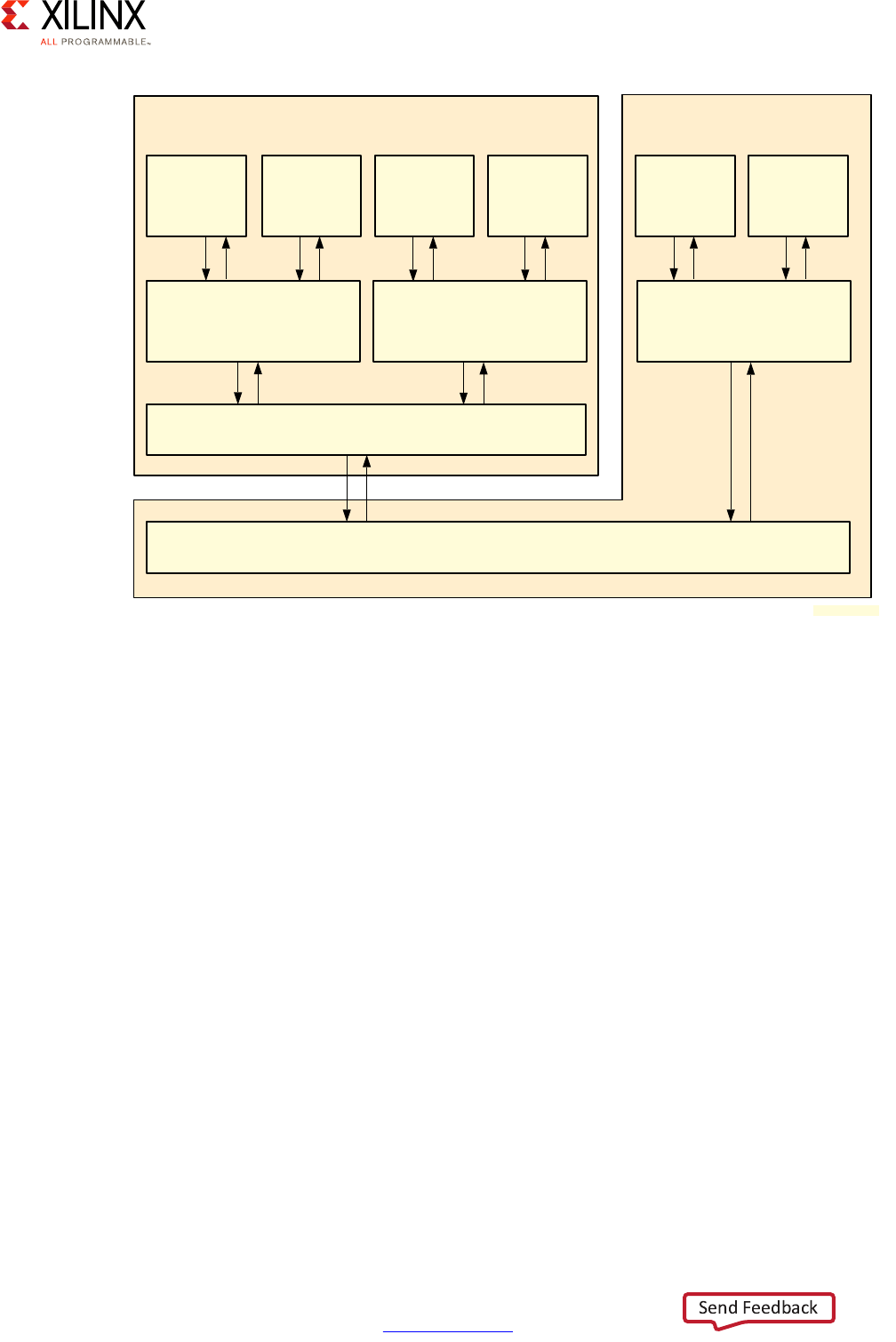
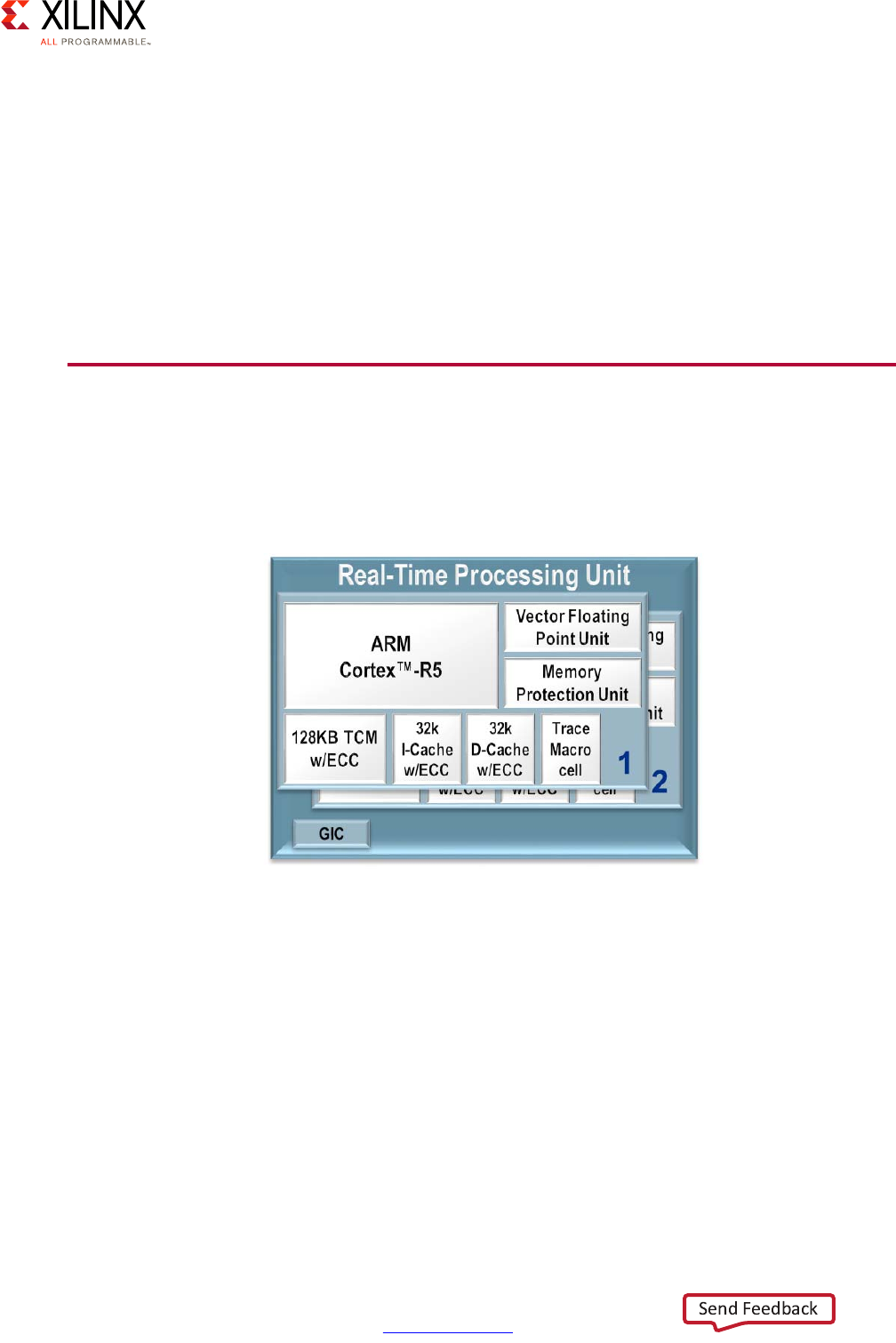
Real-Time Processing Unit (RPU)
The Zynq® UltraScale+™ MPSoC comes equipped with two Cortex-R5 processors which are
typically used for operations requiring deterministic low-latency operations and
response-time critical applications:
Each Cortex-R5 processor provides, among other features:
• ARMv7-R architecture support
•32-bit operation
• Up to 600MHz performance
• Dedicated L1 cache
• 128KB of Tightly-Coupled Memory (TCM) with error-correcting code (ECC)
• Single and double-precision FPU
X-Ref Target - Figure 2-8
Figure 2-8: Real-Time Processing Unit (RPU) Block Diagram
Zynq UltraScale+ MPSoC Embedded Design Methodology Guide 28
UG1228 (v1.0) March 31, 2017 www.xilinx.com
Chapter 2: Processing System
Note that like the case of the APU, while the Cortex-R5 processors can be operated
independently, some of the resources of the RPU, including the Global Interrupt Controller
discussed further below, must be managed coherently for both Cortex-R5 processors in
order for the RPU to operate correctly.
The Cortex-R5 processors can be set to operate in two different modes depending on your
needs:
• Split Mode / Unsupervised AMP:
Also known as the Performance Mode, this is the default mode of the Cortex-R5
processors. In this mode, each core operates independently, except for the interrupt
controller as was just explained. In split mode, one core may be running an RTOS while
another could be running bare-metal, or both could be running different RTOSes. Unlike
the APU, all such configurations in this mode would be considered as unsupervised AMP
as the Cortex-R5 processor cannot support a hypervisor. Communication between the
Cortex-R5 processors could be done by simply passing interrupts and sharing memory
with Xilinx bare-metal libraries or enabling a range of advanced features by means of
advanced features available in OpenAMP framework. Refer to the Zynq UltraScale+
MPSoC OpenAMP: Getting Started Guide (UG1186) [Ref 8] for more information.
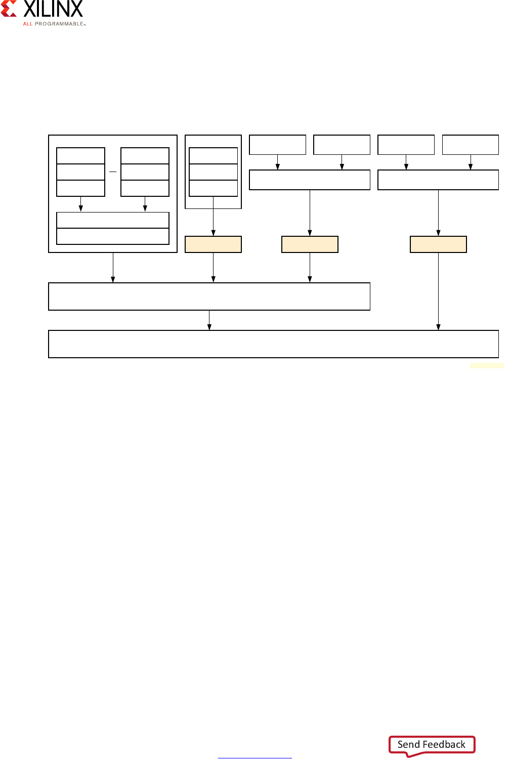
•Lock-Step Mode:
Also known as the Safety Mode, in this mode of operation the Cortex-R5 processors acts
as a single CPU with regards to the rest of the system. Internally, however, the cores are
processing the same instruction in parallel; delayed by 1 ½ clock cycles to allow
detection of single event upsets. Should output from the two cores differ, the
comparison and synchronization logic would detect and signal the error for a
subsequent, custom response. For example tampering could cause the lock-step cores
to get out of sync and, in response to this, you could decide to shut down or lock out the
system. The following diagram illustrates the operation of the RPU in this mode:
X-Ref Target - Figure 2-9
Figure 2-9: Lock-Step of the Cortex-R5 Processors
TCMs Associated
with CPU1
TCM A
TCM B
TCMs Associated
with CPU0
TCM A
TCM B
ShimShim
GIC
Cortex-R5
CPU0
Cortex-R5
CPU1
Caches Associated
with CPU0
D-Cache
I-Cache
Comparison and Synchronization Logic
X15295-092916

Zynq UltraScale+ MPSoC Embedded Design Methodology Guide 29
UG1228 (v1.0) March 31, 2017 www.xilinx.com
Chapter 2: Processing System
If your application is mission critical or if you require functional safety with detection of
single event upsets, then lock-step mode is likely preferable. If, on the other hand, you
would like to benefit from the full performance made possibly by having two Cortex-R5
processors available for your application, the default split mode is best.
As is explained in Chapter 4, Power Considerations, the Cortex-R5 processor are part of
what is known as a “power island” and can be gated together. They cannot, however, be
power gated individually.
The RPU is discussed in more detail in the Real-Time chapter.
Interconnect
The Zynq UltraScale+ MPSoC device's Interconnect is at the heart of its heterogeneous
architecture. It links together all of the processing blocks together and enables them to
interface with the outside world through access peripherals, devices and memory. It's
therefore fundamental to understand its functionality in order to best tune your system.
The Zynq UltraScale+ MPSoC device's interconnect is based on ARM's Advanced eXtensible
Interface (AXI) defined as part of ARM's Advanced Microcontroller Bus Architecture (AMBA)
4.0 specification, and incorporates many other related ARM technologies such as Cache
Coherent Interconnect (CCI-400) and CoreLink NIC-400 Network Interconnect. ARM
describes those technologies in great detail in the corresponding specifications and
documentation it makes available. For the purposes of the present discussion, however, a
brief introduction to the relevant core concepts will prove helpful in determining how to
tweak the Zynq UltraScale+ MPSoC device's interconnect to your needs.
AXI Interfaces
The primary mechanism for linking any pair of blocks within the Zynq UltraScale+ MPSoC
device is an AXI interface. At its most basic level, an AXI interface is specified as linking an
AXI Master to one or more AXI Slaves. The master issues the requests that the slave(s) needs
to fulfill. Each AXI interface consists of five different channels:
• Read Address Channel
• Write Address Channel
• Read Data Channel
• Write Data Channel
• Write Response Channel
Zynq UltraScale+ MPSoC Embedded Design Methodology Guide 30
UG1228 (v1.0) March 31, 2017 www.xilinx.com
Chapter 2: Processing System
The following figures summarize the interaction between master and slave.
Each Zynq UltraScale+ MPSoC device block can contain many interface masters and slaves.
Given the number of components in the Zynq UltraScale+ MPSoC device and the complex
relationships between them, masters and slaves are rarely connected directly. Instead,
several switches are located at strategic points in the Zynq UltraScale+ MPSoC device to
enable the various blocks to connect to one another while keeping with the Zynq
UltraScale+ MPSoC device's emphasis on power management, security, isolation, and
overall flexibility.
X-Ref Target - Figure 2-10
Figure 2-10: AXI Master and Slave Interaction, Read Channels
X-Ref Target - Figure 2-11
Figure 2-11: AXI Master and Slave Interaction, Write Channels
Master
interface
Read address channel
Address
and
control
Read data channel
Read
data
Read
data
Read
data
Read
data
Slave
interface
X12076
Master
interface
Write address channel
Address
and
control
Write data channel
Write
data
Write
data
Write
data
Write
data
Write
response
Write response channel
Slave
interface
X12077

Zynq UltraScale+ MPSoC Embedded Design Methodology Guide 31
UG1228 (v1.0) March 31, 2017 www.xilinx.com
Chapter 2: Processing System
Traffic Priority and Coherency
There is significant parallel traffic occurring at any point in time in the Zynq UltraScale+
MPSoC device. Different processing blocks and resources have however different priorities
while still many parties on the interconnect are accessing the memory simultaneously.
There must therefore be a way to prioritize traffic and, at the same time, preserve the
coherency of traffic going to the memory.
With regards to traffic, not all of it coming in and out of the interconnect switches is given
the same level of priority. Instead, AXI traffic within the Zynq UltraScale+ MPSoC device's
interconnect falls under one of three categories:
• Low Latency (High Priority)
This type of traffic generally needs to be prioritized over other types of traffic. Such is
the case for traffic between the APU and RPU, and the memory.
• High Throughput (Best Effort)
This type of traffic can tolerate higher latencies, but must have very high throughput.
Such is the case of GPU and the PL.
• Isochronous (Video class)
This type of traffic is mostly tolerant of long latencies, except at some critical moments.
Such is the case of video/image data in general. When timeouts are about to expire, this
class of traffic is given the highest priority.
Zynq UltraScale+ MPSoC Embedded Design Methodology Guide 32
UG1228 (v1.0) March 31, 2017 www.xilinx.com
Chapter 2: Processing System
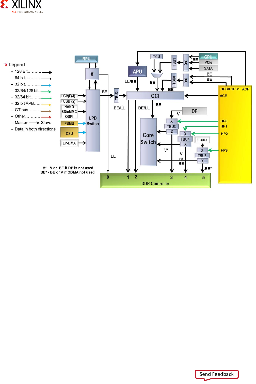
The following diagram provides a simplified view of the Zynq UltraScale+ MPSoC device's
interconnect along with the traffic classes:
The default traffic classes are illustrated as “LL” for Low Latency, “BE” for Best Effort, and “V”
for Video. Many of the blocks in this diagram have already been covered earlier in this
chapter or have been introduced earlier in this section. Note that the TBU and TCU blocks
are part of the SMMU discussed in the previous section. This diagram therefore also shows
the tight relationship between the SMMU and the interconnect.
Apart from the switches, the other key component of the Zynq UltraScale+ MPSoC device's
interconnect is the Cache-Coherent Interconnect (CCI) which ensures that memory
transactions are coherent no matter which parts of the Zynq UltraScale+ MPSoC device are
involved.
X-Ref Target - Figure 2-12
Figure 2-12: Simplified View of Interconnect with Traffic Classes
Zynq UltraScale+ MPSoC Embedded Design Methodology Guide 33
UG1228 (v1.0) March 31, 2017 www.xilinx.com
Chapter 2: Processing System
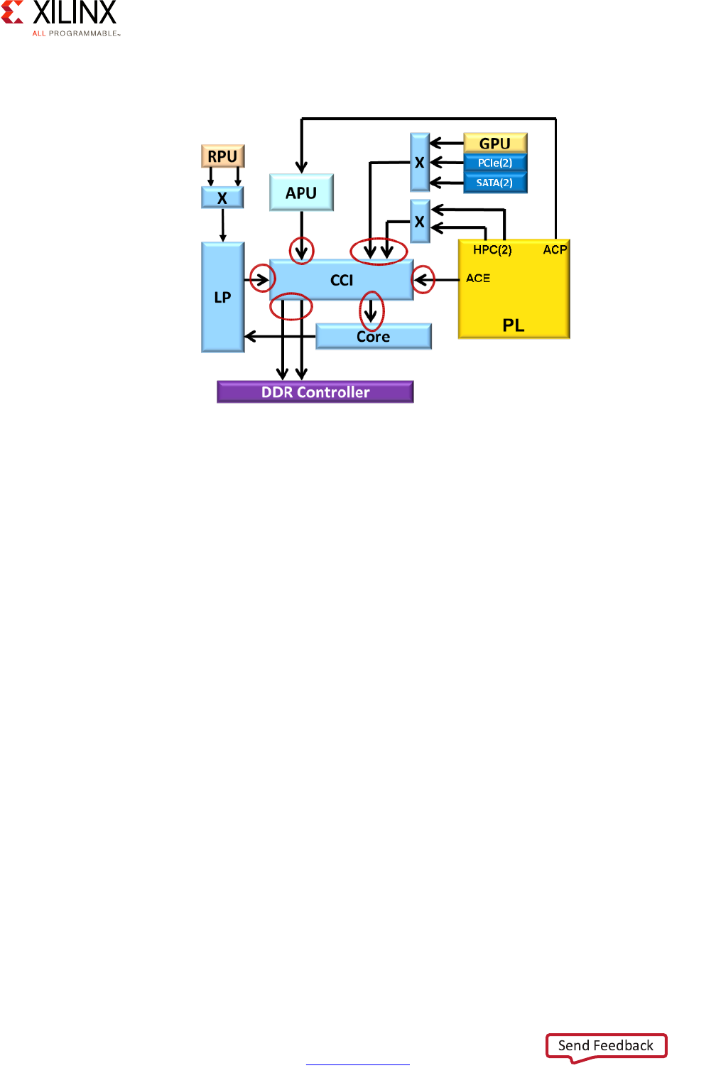
The following diagram highlights the CCI's role:
Detailed View
In addition to the components presented earlier in this section, the Zynq UltraScale+
MPSoC device's interconnect also contains a few additional submodules worth knowing
about:
• AXI Timeout Blocks:
Prevents masters from hanging due to unresponsive slaves
• AXI Isolation Blocks (AIBs):
Manages power-down transitions across system blocks
•XMPU/XPPU:
Enforces isolation between master and slave blocks -- discussed in Chapter 7, Resource
Isolation and Partitioning.
• AXI Trace Macrocell (ATMs):
Retrieves AXI traces for CoreSight using the Advanced Trace Bus (ATB)
• AXI Performance Monitor (APMs):
Captures AXI performance metrics
X-Ref Target - Figure 2-13
Figure 2-13: Role of the CCI
Zynq UltraScale+ MPSoC Embedded Design Methodology Guide 34
UG1228 (v1.0) March 31, 2017 www.xilinx.com
Chapter 2: Processing System
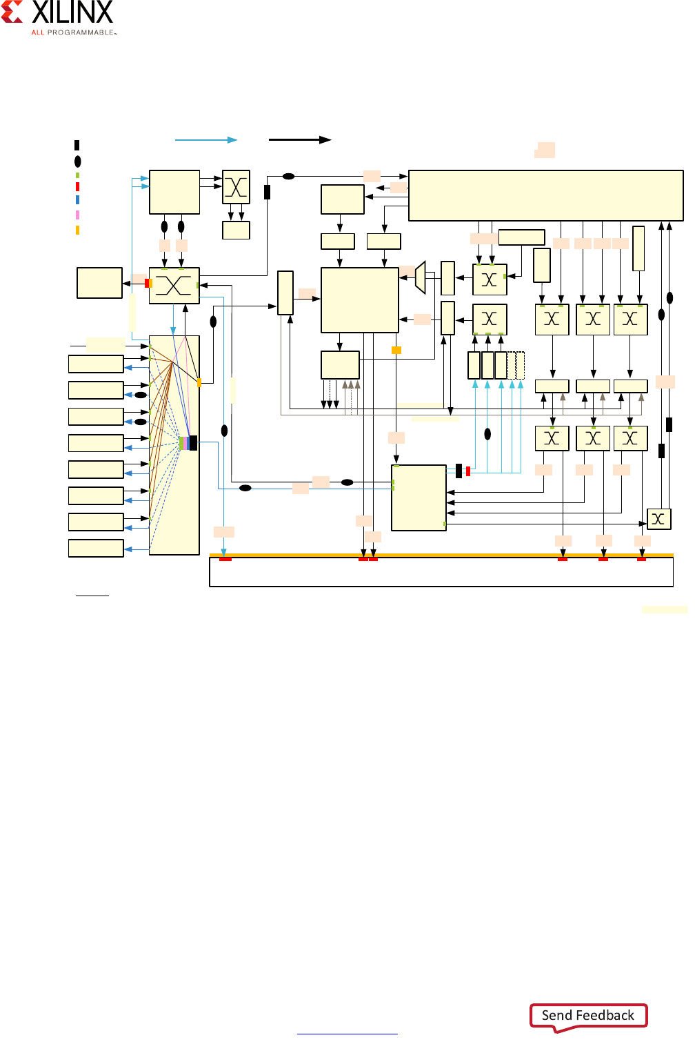
The following diagram captures the detailed view of the Zynq UltraScale+ MPSoC device's
interconnect based on the previous explanations:
Quality of Service (QoS)
Another very important aspect of the interconnect that is illustrated in the previous
diagram is Quality of Service (QoS). There are two parts of the system participating in QoS,
the interconnect switches and the CCI.
Switch-based QoS
If you look closely at the diagram, you will notice that most switches include QoS-400
capabilities. QoS-400 is an ARM addition to the CoreLink NIC-400 standard mentioned
earlier that is used by the Zynq UltraScale+ MPSoC device for its switch interconnect. A
QoS-400 regulator is assigned to most AXI masters in the interconnect.
Note: A QoS-400 “regulator” is the term used in ARM documentation to describe the blocks
associated with AXI masters to control their behavior.
X-Ref Target - Figure 2-14
Figure 2-14: Detailed View of the Zynq UltraScale+ MPSoC Device Interconnect
8
16
16
16
OCM
RPU
USB1
IOU
LPD-DMA
CS-DAP
CSU
Slaves
GIC
APU
ADB ADB
CCI-400
TBU2
TCU
Programmable Logic (PL)
Display
Port
TBU0TBU1
FPD-DMA
PCIe
GPU
SATA
GIC/TCU
Slaves
TBU3 TBU4 TBU5
Core
Switch
DDR Subsystem
2 x 64-bit
S_AXI_LPD
USB0
OCM
AXI Stream
XMPU
XPPU
ATM
PMU
AXI Stream
M_AXI_HPM0_LPD
S_AXI_LPD
S_AXI_ACP_FPD
S_AXI_ACE_FPD
QoS-400
AXI Isolation Block
AXI Timeout Block
ATM+APM
S_AXI_HPC[0:1]_FPD S_AXI_HP[0:3]_FPD
AIB ATB
AIB
AIB
AIB
AIB
ATB
AIB
AIB
AIB
AIB
AIB
ATB
ATB
AIB
M_AXI_
HPM0/1
_FPD
AIB
AIB
ATB
64-bit
MS128-bit
MS
Acronyms
ADB: AMBA Domain Bridge; TCU: Translation Control Unit; TBU: Translation Buffer Unit
16 16 1616
16 16
8
16
8
8
32
32
32
32
32
28
16
ATB
16
16
14,8
8
8
8
8
S3
S2
S1
S0
S4
S3
M0M1
M2
DVM
S5S4S2S1S0
16
The following markings designate the read/write capability of the bus.
Where an example value of 16 designates 16 reads and 16 writes.
Two values (for example 14,8) designates 14 reads and 8 writes. 14,8
X15277-100116
CoreSight
Zynq UltraScale+ MPSoC Embedded Design Methodology Guide 35
UG1228 (v1.0) March 31, 2017 www.xilinx.com
Chapter 2: Processing System
This regulator allows limiting the following for each AXI master:
• Maximum number of outstanding transactions possible at any one time
• Command issue rate
CCI-based QoS
The CCI-400 used in the Zynq UltraScale+ MPSoC device has a QoS Virtual Network (QVN)
feature that is used to avoid the head-of-line blocking (HOLB) effect from occurring during
memory accesses from requests generated by two different traffic priority classes. The
following figure illustrates this scenario:
In this case, one traffic going through the CCI is tagged as Low-Latency while the other is
tagged as Best Effort. HOLB would occur if the lower priority traffic, namely Best Effort,
would "hold the line" (i.e. a DDR port) from the higher priority traffic, namely Low Latency.
The QVN uses different queues and tokens to arbitrate the traffic between the two DDR
ports and avoid the delay caused by HOLB.
This is helpful in the case of the APU as it isn't confined to using a single preassigned DDR
port and is instead switching constantly between the two DDR ports attached to the
CCI-400 to which the APU is itself attached; see the diagram from the previous section.
Since the APU's traffic is generally Low-Latency and most other traffic sharing the CCI with
it is Best Effort, the use of QVN as just explained ensures the APU gets the appropriate QoS
for its memory accesses.
X-Ref Target - Figure 2-15
Figure 2-15: CCI-based QoS
CCI-400
LL Traffic BE Traffic
DDR Controller
Port 1 Port 2
X15889-101816

Zynq UltraScale+ MPSoC Embedded Design Methodology Guide 36
UG1228 (v1.0) March 31, 2017 www.xilinx.com
Chapter 2: Processing System
Customizing QoS
In the vast majority of cases there is no need to modify the QoS setup used by default in the
Zynq UltraScale+ MPSoC device. However, if you are having issues and would like to
possibly tweak some of the QoS-400 regulators, for instance, start by using the built-in data
collection capabilities made possible by the APMs and ATMs mentioned earlier. Xilinx
Software Development Kit (SDK) User Guide: System Performance Analysis (UG1145) [Ref 11]
helps you use the performance monitoring capabilities of the freely-available Xilinx
Software Development Kit (SDK) to model traffic and retrieve live runtime information from
the Zynq UltraScale+ MPSoC device. You can also do the same with the SDSoC
Development Environment. This is a unique feature of Xilinx enabling you not just to
retrieve information from the APU but from the rest of the interconnect connecting all the
Zynq UltraScale+ MPSoC device's internal blocks.
With the data from these tools, and review of the full interconnect diagram shown earlier,
you can identify hot paths in your system and adjust its configuration as necessary. This is
typically done by identifying which traffic from which AXI masters is being negatively
impacted by traffic from lower priority masters. You can then throttle the less important AXI
masters by tweaking their corresponding QoS-400 regulators. If the traffic from the APU
and the RPU is less important than that of the PL, for example, you can configure the APU's
and RPU's regulators to favor traffic from the PL instead. To effectively pull this off, however,
you must make sure that you have a solid understanding of the traffic flow within the Zynq
UltraScale+ MPSoC device.
Only pursue this if the default settings don't work for your design.
PL Interfaces
One aspect of the Zynq UltraScale+ MPSoC device interconnect that is under the designer's
full control are the connections between the PL and the rest of the system. As can be seen
in the main interconnect diagram presented earlier and as will be discussed in Chapter 5,
Programmable Logic, there are several paths from the PL to the interconnect and therefore
the rest of the system. The explanations found in Chapter 5 build on the explanations
provided earlier in this section.

Zynq UltraScale+ MPSoC Embedded Design Methodology Guide 37
UG1228 (v1.0) March 31, 2017 www.xilinx.com
Chapter 2: Processing System
Additional Information
For additional information regarding the interconnect, refer to the corresponding chapter
in Zynq UltraScale+ MPSoC Technical Reference Manual (UG1085) [Ref 7], as well as the
official ARM documentation regarding:
• AMBA 4.0–the core AXI standard
• NIC-400–the switch interconnect
• CCI-400–the cache coherent interconnect
• QoS-400–the QoS addition to NIC-400
Interrupts
With its highly integrated, heterogeneous design the Zynq UltraScale+ MPSoC device
comprises a large number of interrupt sources and several ways of handling them. Most of
the integrated peripherals, for instance, trigger interrupts to notify processors of important
events; this includes Ethernet, USB, GPU, DisplayPort, DMA, UART, SPI, SD, etc. The PL can
also trigger 16 different interrupts.
Additionally, the Zynq UltraScale+ MPSoC device includes configurable Inter-Processor
Interrupts (IPIs) that can be used to enable the independent processing blocks to
communicate with each other.
There are two interrupt controllers in on the Zynq UltraScale+ MPSoC device, one for the
APU and one for the RPU. The APU's interrupt controller implements the ARM Global
Interrupt Controller version 2 (GICv2) specification while the RPU's interrupt controller is
based on the ARM GICv1 specification. A key benefit of the former is enabling interrupt
virtualization on the APU.
Zynq UltraScale+ MPSoC Embedded Design Methodology Guide 38
UG1228 (v1.0) March 31, 2017 www.xilinx.com
Chapter 2: Processing System
The following diagram illustrates the Zynq UltraScale+ MPSoC device's interrupt routing:
The block marked GIC-400 is the APU's GICv2 interrupt controller while the block marked
GIC (PL390) is the RPU's GICv1 interrupt controller.
APU Interrupt Controller
Each Cortex-A53 processor has four interrupt lines as input:
• nIRQ are normal priority interrupts
• nFIQ are high-priority or Fast Interrupts
• nVIRQ are normal priority virtual interrupts, for virtualization support on the APU
• nVFIQ are high priority virtual interrupts, for virtualization support on the APU
X-Ref Target - Figure 2-16
Figure 2-16: Zynq UltraScale+ MPSoC Device Interrupt Routing
Cortex-A53 MPCore
CPU0 CPUn
CPU0 I/F
VCPU0 I/F CPU0 I/F
VCPUn I/F
Distributor
RPU Cores
CPU0 CPU1
GIC (PL390)
CPU0 I/F CPU1 I/F
Distributor
niRQ0/nFIQ0
nViRQ/nVFIQ
niRQ0/nFIQ0 niRQ1/nFIQ1
Interrupt Source Blocks
(e.g., VCU, GPU,
DisplayPort)
PCIe
Top Level IPI
PCIe Inbound
To Interconnect
To PMU
To PL
To PMU
To PMU
MSI
Legacy IRQ/FiQ per CPU From PL
APU
GIC-400
X15327-092816
Zynq UltraScale+ MPSoC Embedded Design Methodology Guide 39
UG1228 (v1.0) March 31, 2017 www.xilinx.com
Chapter 2: Processing System
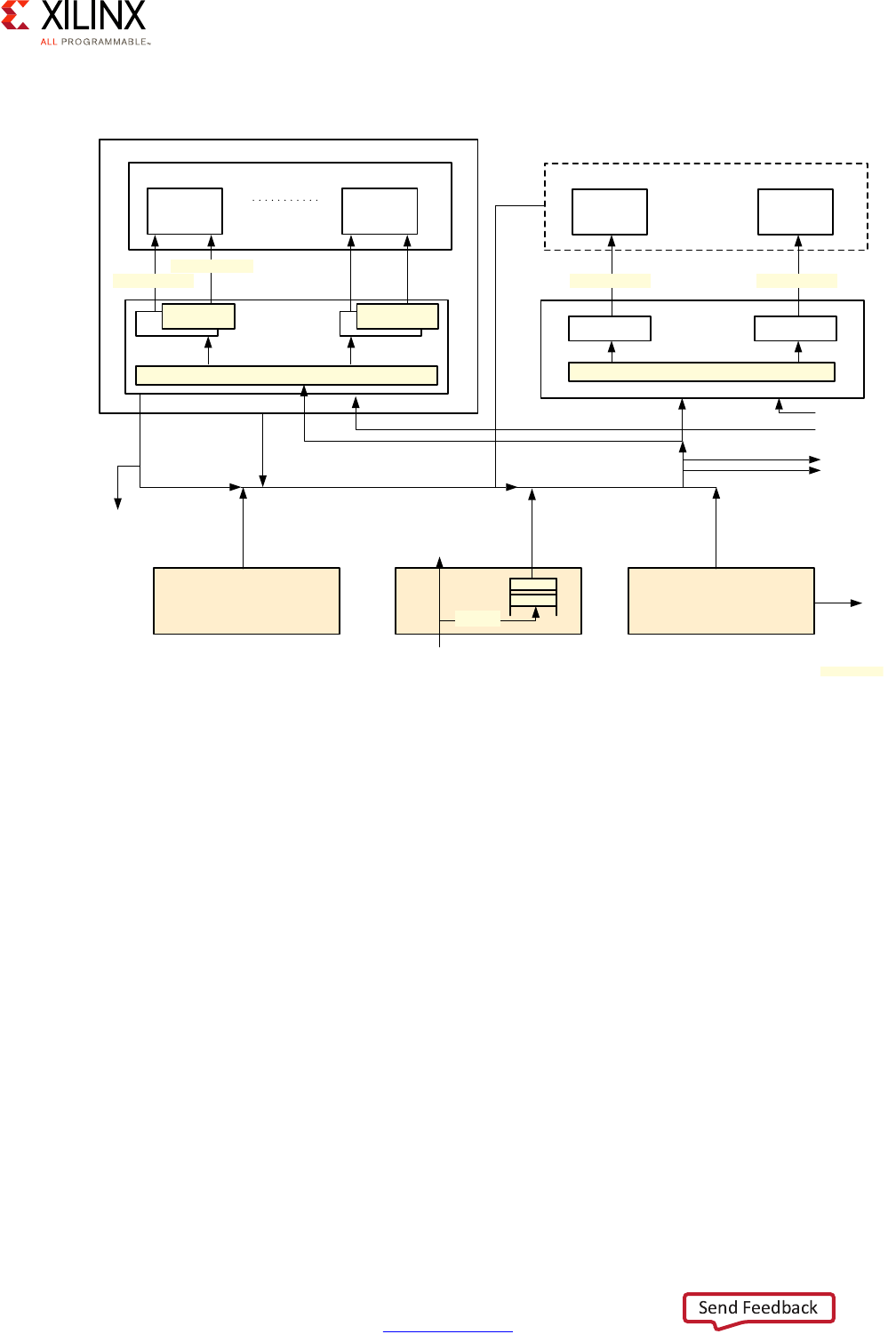
The APU's interrupt controller handling of the Cortex-A53 processors' interrupts is
illustrated in the following figure:
The interrupt controller is separated into 2 parts. The distributor is responsible for
registering the inbound interrupts and prioritizing them before distributing them to the
right target CPU. The second part of the interrupt controller interfaces with each CPU's
interrupt lines to trigger the actual interrupt on the relevant Cortex-A53 processor.
The interrupt controller handles 3 types of interrupts:
• 16 Software Generated Interrupts (SGI) for sending interrupts between cores
• 7 Private Peripherals Interrupt (PPI) are targeted to a single Cortex CPU core
• 92 Shared Peripherals interrupts (SPI) shared between all APU and RPU cores
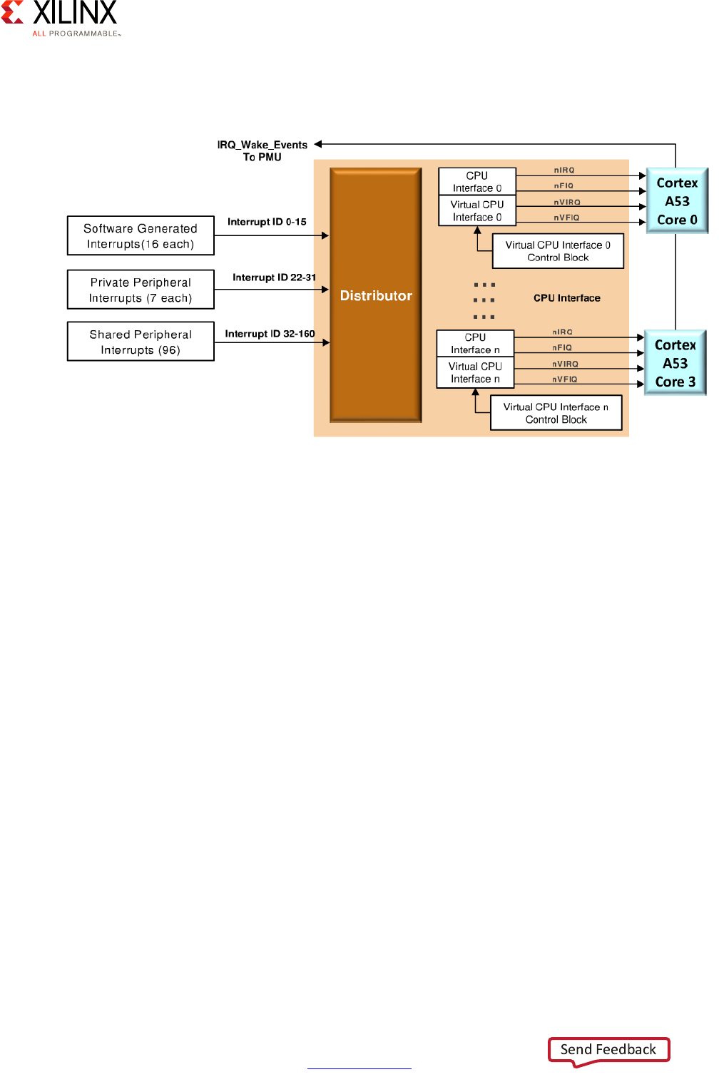
APU Interrupt Virtualization
When an interrupt is received while the APU is running a hypervisor, the hypervisor will
interface with the APU's interrupt controller to generate virtual interrupts for the guest
OSes as illustrated below. Those interrupt will be delivered directly to the guest OS which
will handle and clear them. The hypervisor can handle and clear interrupts locally if the
interrupt isn't meant to reach guests.
X-Ref Target - Figure 2-17
Figure 2-17: APU Interrupt Controller
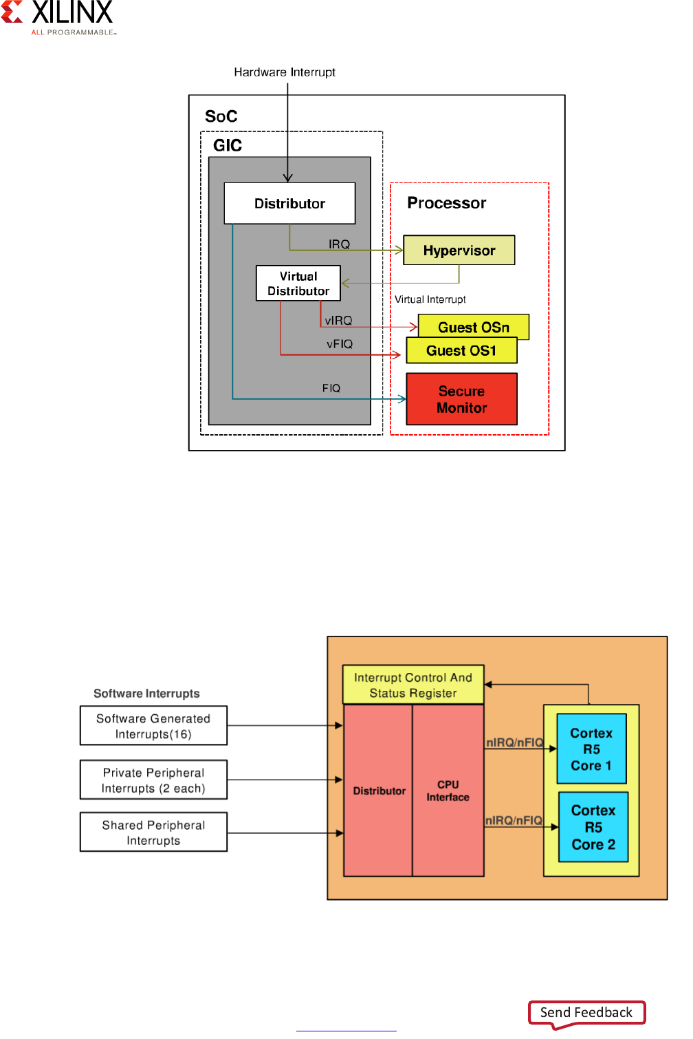
Zynq UltraScale+ MPSoC Embedded Design Methodology Guide 40
UG1228 (v1.0) March 31, 2017 www.xilinx.com
Chapter 2: Processing System
RPU Interrupt Controller
The RPU's GICv1 interrupt is attached to the Cortex-R5 processors as shown below. It's
similar to the APU's interrupt controller but doesn't support virtual interrupts. It also
handles fewer interrupts for each of the previously-mentioned types (i.e. SGI, PPI, SPI).
X-Ref Target - Figure 2-18
Figure 2-18: APU Interrupt Virtualization
X-Ref Target - Figure 2-19
Figure 2-19: RPU Interrupt Controller
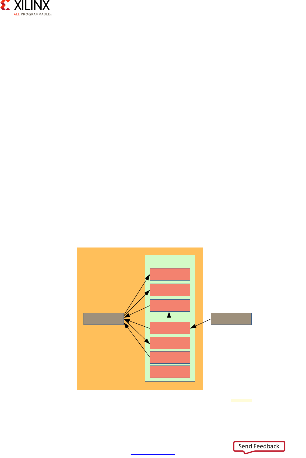
Zynq UltraScale+ MPSoC Embedded Design Methodology Guide 41
UG1228 (v1.0) March 31, 2017 www.xilinx.com
Chapter 2: Processing System
Secure State and Interrupts
As will be explained in Chapter 7, Resource Isolation and Partitioning, all of the Zynq
UltraScale+ MPSoC device's blocks connected through the interconnect are categorized as
either secure or non-secure, per the ARM TrustZone specification. While the details will be
covered in Chapter 7, note that the interrupt controllers of both the APU or the RPU do not
distinguish between the party triggering an interrupt as either being secure or non-secure.
By convention, FIQs on the APU are sent to the secure monitor but this is a software choice,
not a hardware requirement.
Inter-Processor Interrupts
Inter-Processor Interrupts (IPIs) are the underpinning of communication between
processing blocks in the Zynq UltraScale+ MPSoC device, providing a channel to interrupt
a remote processor and carry and can carry a certain amount of payload. One of the main
uses of IPI, for instance, is power management. If the full power domain is powered down,
an IPI can be sent to the PMU to request that it be powered back on.
There are 11 IPI channels among which 4 are reserved for communication with the Platform
Management Unit (PMU). Each IPI channel, except some reserved to communication with
the PMU, have two 32 byte buffers and 6 registers that are used for communication
between the source and target. The first buffer is used by the master to store the request
and the second one is used by the target to store the response. The figure below illustrates
how the registers are manipulated by the master to trigger an IPI and by the target to
acknowledge and reply to the interrupt.
X-Ref Target - Figure 2-20
Figure 2-20: Inter-Processor Interrupt Channel Registers
Enable
Trigger
Observation
Status/Clear
Disable
Mask
Req/Resp buffers
Master A Master B
IPI Channel
X18707-032117
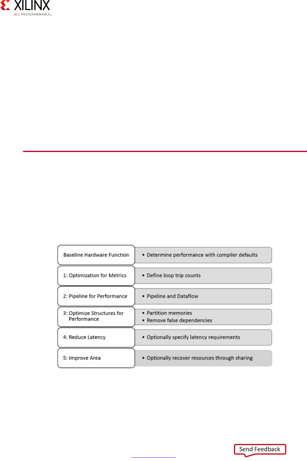
Zynq UltraScale+ MPSoC Embedded Design Methodology Guide 42
UG1228 (v1.0) March 31, 2017 www.xilinx.com
Chapter 2: Processing System
OpenAMP
Using IPIs directly for cross-block communication within the Zynq UltraScale+ MPSoC
device can be tedious. Xilinx therefore provides the OpenAMP framework, discussed in
greater detail in Chapter 3, System Software Considerations, to facilitate the development
of AMP systems in a heterogeneous environment. OpenAMP is built on IPIs and exposes
two key components to allow CPU cores to communicate:
• Remoteproc: for starting and managing the life cycle of remote CPUs
• RPMsg: for communicating between remote CPUs.
Refer to Chapter 3, System Software Considerations for more information about OpenAMP
and its usage.
Workload Acceleration Using the PL
As mentioned in Processing System Methodology, page 14, the Zynq UltraScale+ MPSoC
device's PL can be used to offload processing through hand coding, or by way of using
either the Vivado® HLS or the Xilinx SDSoC development environments. This, therefore,
enables system designers to easily move software to the PL for performance acceleration.
The process to offloading processing to the PL using SDSoC can be summarized as follows:
X-Ref Target - Figure 2-21
Figure 2-21: PL Offloading Process Summary
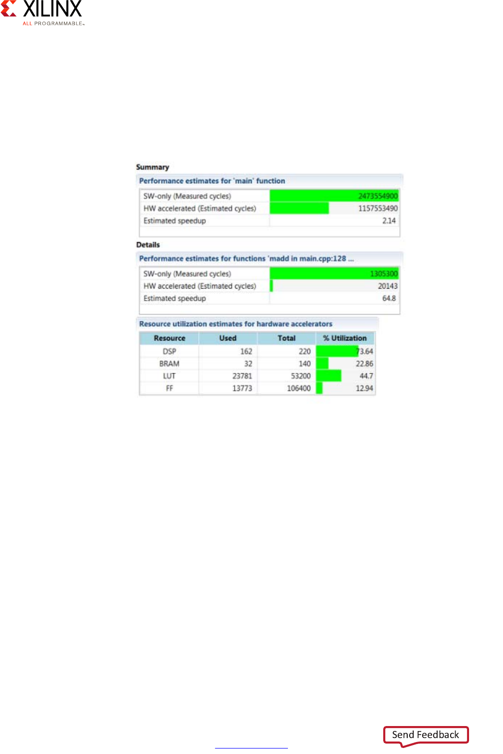
Zynq UltraScale+ MPSoC Embedded Design Methodology Guide 43
UG1228 (v1.0) March 31, 2017 www.xilinx.com
Chapter 2: Processing System
SDSoC has several features which allow developers to analyze the performance of an
application running on MPSoC hardware. It allows developers to identify repetitive
segments of code by generating a complete report on the code. That report identifies if the
code built in the environment can be improved by offloading to the PL and gives an
estimation of how it would improve the performance of the system along with how much it
would cost in terms of PL resources. The screen capture below is an example of the type of
information the SDSoC environment can give.
The C/C++ code can then be converted into a block placed inside the ZU's PL. This step is
done using the Vivado HLS (for High-Level Synthesis) compiler.
After synthesis, a report about selection of the Data Movers by the synthesis environment
is available to the developer. SDSoC automatically chooses your data movers and drivers,
but these can be easily overridden by user control if desired. It is also possible to generate
calling wrappers to allow applications running on the APU or the RPU to call into IP blocks
generated in Verilog or VHDL in the PL section of the board. This technique skips the HLS
compilation just described.
X-Ref Target - Figure 2-22
Figure 2-22: Example PL Acceleration Output by SDSoC
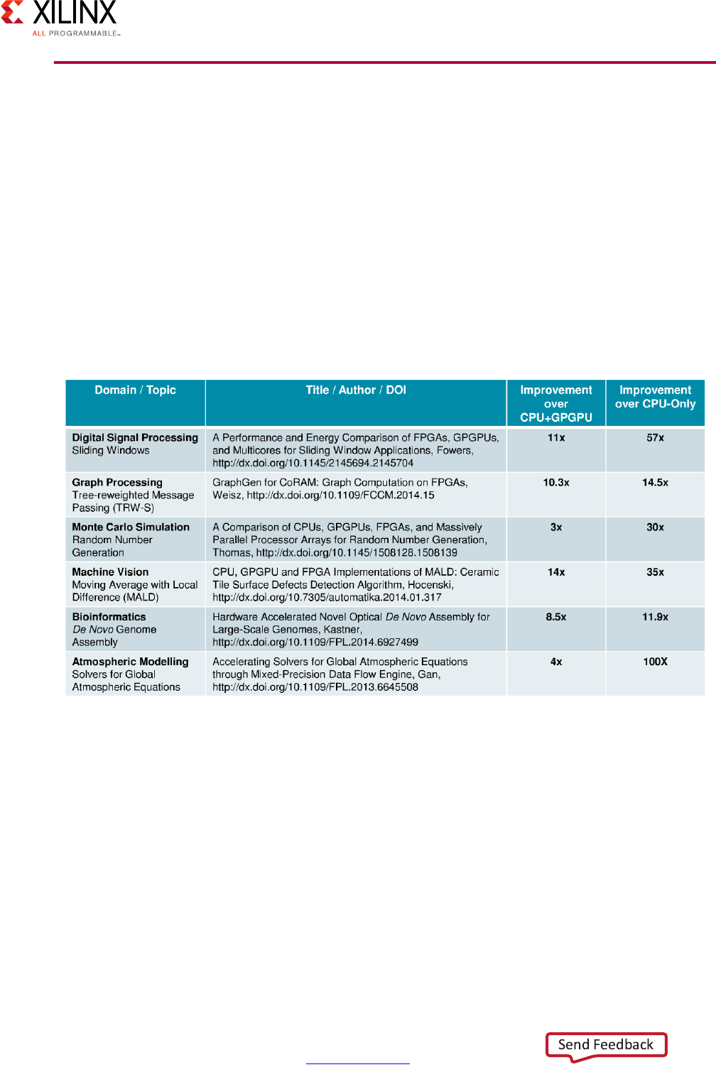
Zynq UltraScale+ MPSoC Embedded Design Methodology Guide 44
UG1228 (v1.0) March 31, 2017 www.xilinx.com
Chapter 2: Processing System
General-Purpose Computing Acceleration
Aside from the targeted work of either manually or automatically offloading workloads to
the PL covered in the previous section, there are several commonly-used techniques and
technologies for accelerating general-purpose computing. These include the use of OpenCL
libraries and general-purpose computing on graphics processing units that support GPGPU.
The Zynq UltraScale+ MPSoC device's PL offloading capabilities just discussed offer a
compelling computational acceleration path when compared to other industry techniques.
The MALI-400 GPU used in the Zynq UltraScale+ MPSoC device is architectured exclusively
for graphics acceleration and isn't suitable for GPGPU.
The following table shows independently-published results where optimization through
FPGA beats the combination of a general-purpose GPU and CPU:
Finally, the table below provides the general reasons why using the PL (i.e. FPGA) might give
better results than using the GPGPU for acceleration:
X-Ref Target - Figure 2-23
Figure 2-23: FPGA vs. CPU+GPGPU and CPU-Only Optimizations
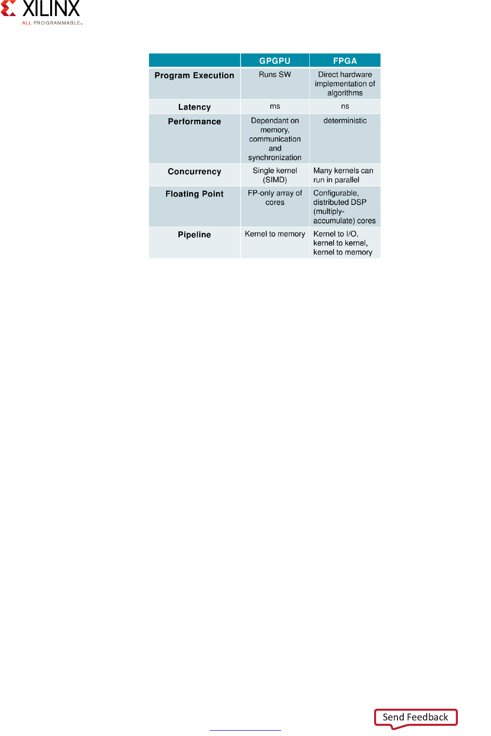
Zynq UltraScale+ MPSoC Embedded Design Methodology Guide 45
UG1228 (v1.0) March 31, 2017 www.xilinx.com
Chapter 2: Processing System
In sum, if you are looking for accelerating software, we strongly encourage you to explore
the PL's offloading capabilities. Apart from the SDSoC tool mentioned earlier, another tool
you might want to consider is the Xilinx SDAccel™ Development Environment. SDAccel is
tailored for OpenCL, C and C++ acceleration on FPGA.
X-Ref Target - Figure 2-24
Figure 2-24: FPGA Acceleration Benefits Compared to GPGPU

Zynq UltraScale+ MPSoC Embedded Design Methodology Guide 46
UG1228 (v1.0) March 31, 2017 www.xilinx.com
Chapter 3
System Software Considerations
Software across the Zynq® UltraScale+™ MPSoC permeates virtually all areas of the device.
Software can exist as Bare Metal applications, middleware, firmware, drivers, high level
operating systems (HLOS), libraries, high level applications, graphics applications,
communication protocols, and so forth. Depending on your specific Zynq US+ MPSoC
application, the software components across the silicon can be included or excluded,
enable specific hardware features, affect speed and efficiency of the device, and in general
provide the overriding execution environment you desire. In short, your particular software
footprint is the glue for your system.
Defining Your System Software Needs
Given the software flexibility afforded by the Zynq UltraScale+ MPSoC device and yet its
importance to unlocking the Zynq UltraScale+ MPSoC device's full potential, designers
must ensure that they have a strong understanding of the software options available for use
with the Zynq UltraScale+ MPSoC device's various parts. This chapter guides you through
the software choices available for the Zynq UltraScale+ MPSoC device along with the
relevant recommendations.
Answering the following questions will help you define your design's needs with regards to
the Zynq UltraScale+ MPSoC device:
1. Would you prefer running bare metal or using an OS?
2. If you'd prefer bare metal, what are the specific reasons behind this choice?
3. Do you need real-time capabilities?
4. Do you have any boot time constraints? If so, how firm are those?
5. What is your preferred build or development environment?
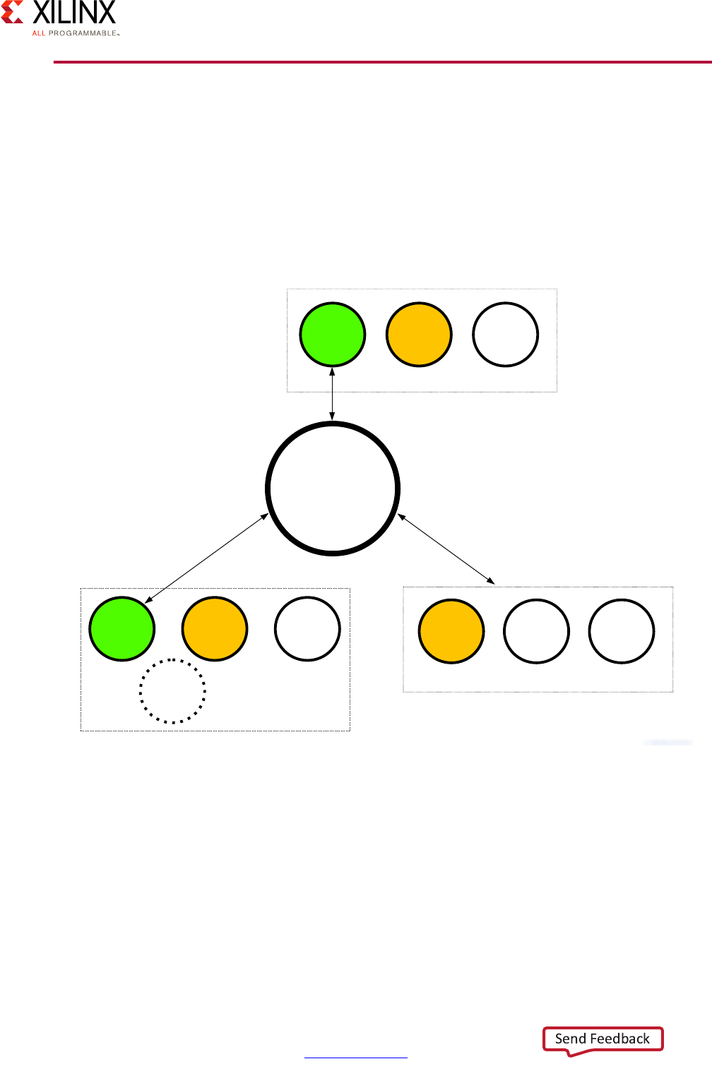
Zynq UltraScale+ MPSoC Embedded Design Methodology Guide 47
UG1228 (v1.0) March 31, 2017 www.xilinx.com
Chapter 3: System Software Considerations
System Software Methodology
Note: The Zynq UltraScale+ MPSoC platform can run a wide range of independent software
stacks simultaneously on multiple processing blocks in the system. The following diagram is
a simplified conceptual view of the full system diagram presented in this guide's
introduction that highlights the processing blocks, with blocks in green being most flexible
for running any kind of software. Yellow and white blocks have decreasing levels of
flexibility, in that order.This diagram does NOT attempt to precisely represent the internal blocks
of the Zynq UltraScale+ MPSoC device. Instead, it is primarily a conceptual view for the purposes of
the present explanation.
X-Ref Target - Figure 3-1
Figure 3-1: Simplified Software View of the Zynq UltraScale+ MPSoC Device
RPU PMU
LPD
Peripherals
Inter-Processor
Communication
Framework
(OpenAMP)
APU GPU*
CSU
PL
FPD
Peripherals
Full Power Domain
Low Power Domain
Programmable Logic Power Domain
PL
Peripherals Accelerators
A
cce
l
erators
* GPU support is OS-specific
X18660-032917

Zynq UltraScale+ MPSoC Embedded Design Methodology Guide 48
UG1228 (v1.0) March 31, 2017 www.xilinx.com
Chapter 3: System Software Considerations
The application processing unit (APU) and real-time processor unit (RPU), comprising
general-purpose ARM A53s and ARM R5s, can be made to run any software that typically
runs on embedded processors. The graphics processing unit (GPU), platform management
unit (PMU) and processing logic (PL), being built with specific functionality in mind, are
more constrained in terms of what can be done with them software-wise. The GPU's
functionality is typically accessible through the graphic and multimedia libraries and drivers
made available by Xilinx. Xilinx provides a default firmware for the PMU and, while custom
PMU firmware versions can be created, it's strongly recommended to use that default
firmware as-is. The PL can also be made to run software in two ways: 1) by optimizing parts
of software into hardware, or 2) by running MicroBlaze™ processor soft-core instances.
Note that as in the case in Figure 3-1, page 47, the configuration security unit (CSU) block
is illustrated with a dotted line because it is programmed from factory and therefore not
customizable in any way.
Power management is central to the Zynq UltraScale+ MPSoC device's architecture and it's
therefore an important aspect to keep in mind when deciding the software components to
use on each block. As is explained in Chapter 2, Processing System, the Zynq UltraScale+
MPSoC device has several power domains that can be controlled at runtime. If, for instance,
you choose to run Linux on the APU, that OS becomes unavailable while the Full Power
Domain is powered off.
This chapter covers the APU and RPU's software capabilities in detail. It also introduces the
software available for using the GPU and the functioning of the default PMU firmware. For
more information regarding graphics, including the GPU, refer to Chapter 9, Multimedia,
and for more information regarding power management, including the PMU, refer to
Chapter 4, Power Considerations. The PL's hardware offloading capabilities are covered in
Chapter 2, Processing System. Refer to the general Xilinx® MicroBlaze documentation for
information regarding using MicroBlaze soft-cores in Xilinx PL.
Application Processing Unit Software
The APU is the Zynq UltraScale+ MPSoC device's main general-purpose processing block.
With up to four A53s running at up to 1.5GHz, it is capable of delivering significant
computing power and supporting powerful software abstractions.
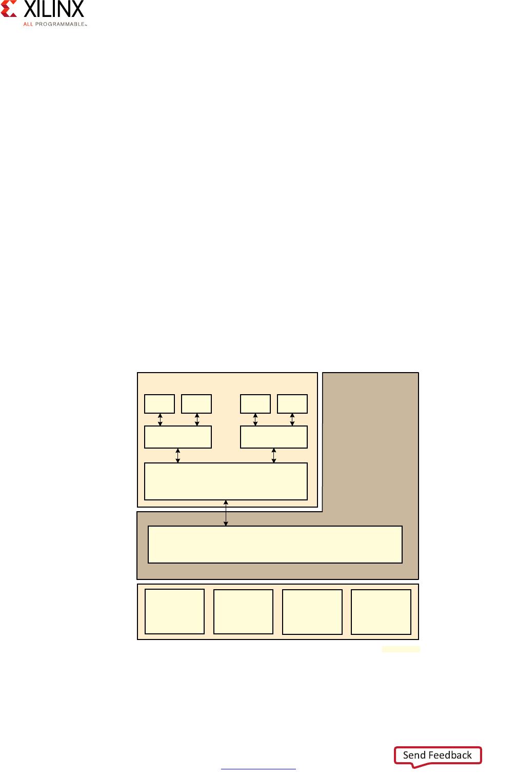
Zynq UltraScale+ MPSoC Embedded Design Methodology Guide 49
UG1228 (v1.0) March 31, 2017 www.xilinx.com
Chapter 3: System Software Considerations
The following software and software configurations are available on the APU:
• Bare metal operation, either directly on the A53s or as a guest on the Xen Hypervisor.
Note: While useful on a single A53, this is not scalable across multiple A53s.
• Full-fledged SMP Linux, either directly on the A53s or as a guest on the Xen Hypervisor.
• FreeRTOS, either directly on the A53s or as a guest on the Xen Hypervisor.
Note: While useful on a single A53, this is not scalable across multiple A53s.
• Xen Hypervisor for either hosting guest Linux instances or running Linux instances on
some A53s.
• ARM Trusted Firmware (ATF) for supporting the TrustZone capabilities of the A53, as
discussed in Chapter 7, Resource Isolation and Partitioning.
• Xilinx Open Asymmetric Multi Processing (OpenAMP), the framework enabling
communication between software running across different Zynq UltraScale+ MPSoC
device blocks.
• Relevant Drivers, Services, and Libraries for any of the above.
Here is an example configuration of the APU that enables running many of the packages
previously mentioned.
X-Ref Target - Figure 3-2
Figure 3-2: Example APU Software Stack
Non-secure world
Xen Hypervisor
Guest OS Guest OS
App1 App2 App1 App2
Secure world
ARM Trusted Firmware (ATF)
A53
Core 0
A53
Core 1
A53
Core 2
A53
Core 3
X18930-032117

Zynq UltraScale+ MPSoC Embedded Design Methodology Guide 50
UG1228 (v1.0) March 31, 2017 www.xilinx.com
Chapter 3: System Software Considerations
In this case, the APU is simultaneously running the ARM Trusted Firmware (ATF) along with
the Xen hypervisor and two separate guest OSes. The APU is therefore segregated in two
important ways. First, there is a secure and non-secure environment, which is made possible
by the ARMv8 TrustZone feature that will be covered in Chapter 7, Resource Isolation and
Partitioning. Second, there are two distinct guest OSes running side by side, as made
possible by the Xen hypervisor.
Bare Metal Use of the APU
If you are approaching the Zynq UltraScale+ MPSoC device and at first feel that it would be
preferable to use it bare metal (that is, without using any OS or hypervisor) in its entirety, it's
strongly recommended that you carefully analyze the reasons behind this inclination,
especially with regards to the APU. While APU supports running bare metal, only one A53
can be used for this use case, therefore making the other 3 A53s unusable. So, you should
carefully weigh this before architecting your system. The reason behind this is that Bare
Metal does not support SMP operation. This is not so much a hardware limitation, as both
Xen and Linux are capable of managing the APU's many A53s, but rather a matter of the
significance of the effort and the complexity of the software involved.
Hence, if you are interested in using the APU bare metal or are undecided:
1. RPU provides the best real-time interrupt response on a processor with 600 DMIPS.
2. Running bare-metal on the APU can provide real-time response that is adequate for a
large number of designs, but at the expense of difficulty to utilize all APU processor
cores.
Running bare-metal on a hypervisor alongside other operating systems has also been
shown to meet key product requirements where a very fast and tightly-distributed real-time
is not necessary.If your concern is hard real-time response times then the follow-up
question you need to answer is whether or not the real-time code needs to be tightly tied
to Linux. If the real-time code is fairly standalone then chances are the RPU is a much better
candidate for running it. If there is a dependency between the real-time code and Linux,
we'd still recommend you first look at running the real-time portions on the RPU and use
the OpenAMP framework to communicate back to a Linux instance running on the APU
when needed. Ultimately, if even using OpenAMP does not solve your problem then you
might want to consider one of Linux's real-time variants, available from third parties, on the
APU or the use of a suitably performing hypervisor to host bare-metal and/or RTOS
alongside Linux on the APU.
If your application does not require the strictest real-time performance, then execution of
bare-metal applications on top of Xen hypervisor has proven to be viable. Xen can enable
you to have full control over the software running on the A53s without actually requiring
you to run Linux as a guest. You can therefore run bare metal code on separate A53s with
Xen.
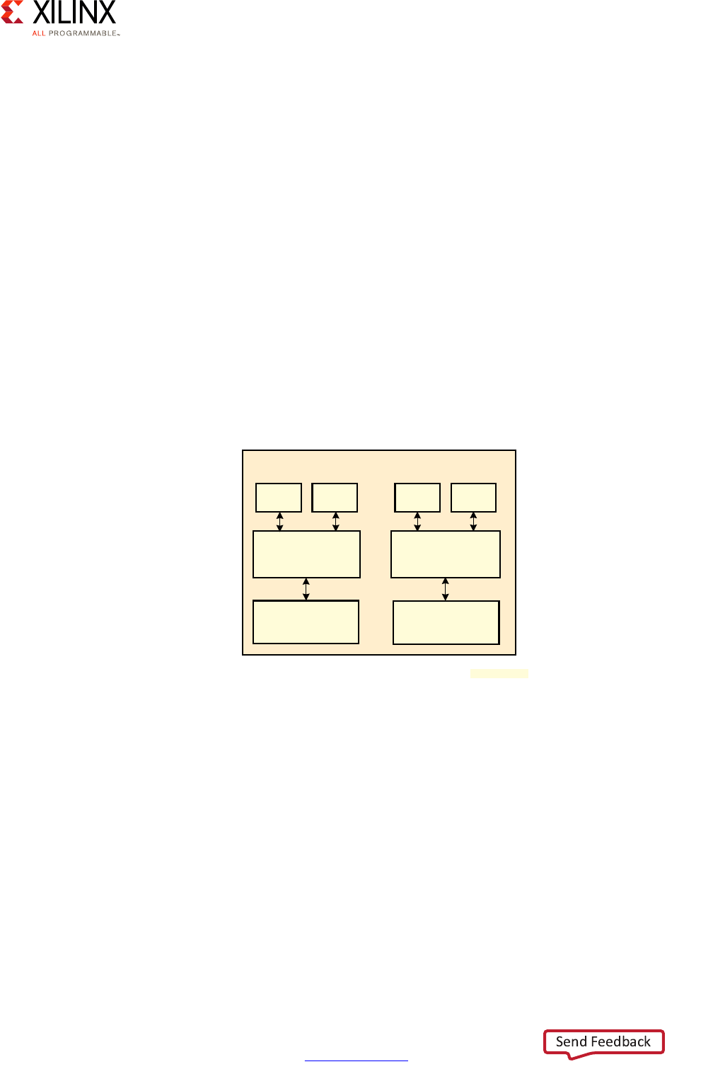
Zynq UltraScale+ MPSoC Embedded Design Methodology Guide 51
UG1228 (v1.0) March 31, 2017 www.xilinx.com
Chapter 3: System Software Considerations
Real-Time Processing Unit (RPU) Software
The Zynq UltraScale+ MPSoC device's inclusion of the RPU as a fully independent block
alongside the APU opens the way for designers to collocate both real-time and general
purpose computing workloads on the same system without having to compromise on
either. By providing a dedicated real-time processing environment, the RPU's two R5s free
the designer from attempting to achieve near-real-time performance with the APU's
general purpose A53s. While the A53s run industry-standard, general purpose high-level
functionality and operating systems, the RPU can simultaneously run:
• Bare metal applications
• FreeRTOS and other commercially available RTOS.
• The OpenAMP framework enabling communication with other processing blocks
• Relevant Drivers, Services, and Libraries for any of the above
Note that the RPU's R5 can either be run in split or in lock-step mode. In split mode, each
R5 can run its own software stack as is illustrated here:
As explained in Chapter 2, Processing System, in lock-step mode one of the R5s shadows
the other R5's operation and an error can be triggered if their outputs differ. When run in
lock-step, the available Tightly Coupled Memory (TCM) combines to make 256 KB available
to the RPU.
The R5s can be made to boot independently from the FSBL at startup or they can be
operated as slaves to the APU. In slave mode, OpenAMP is used on the APU to load and
reset the R5s with a designated workload at runtime.
X-Ref Target - Figure 3-3
Figure 3-3: Example RPU Software Stack
RPU
R5 Core 0
Baremetal
RTOS
Baremetal
RTOS
App1 App2 App1 App2
R5 Core 1
;
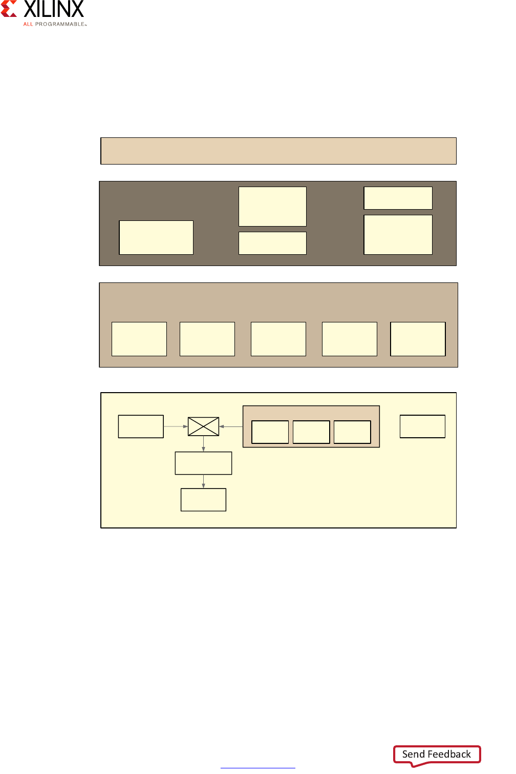
Zynq UltraScale+ MPSoC Embedded Design Methodology Guide 52
UG1228 (v1.0) March 31, 2017 www.xilinx.com
Chapter 3: System Software Considerations
Graphics Processing Unit Software
The Zynq UltraScale+ MPSoC device uses the industry-standard ARM Mali-400 MP2
graphics processing unit (GPU) for 2D and 3D graphics. The following figure shows the
system components involved in the use of the GPU with a Linux-based software stack.
Applications using the GPU sit on top of middleware that include a display server (e.g.
Wayland), graphics libraries (such as OpenGL ES 1.1), Mali common libraries, Gstreamer, and
Video codecs. Layered between the middleware and the actual GPU hardware components
are the Linux kernel drivers. These drivers handle buffering frames, DRAM, Mali graphics,
video, and display.
X-Ref Target - Figure 3-4
Figure 3-4: GPU Software Stack on Linux
Graphics Application
Display Server
Ex: XII, Wayland Mali common
Libraries
Video Codecs
Graphic Libraries
Ex: Open GLES1,
Open GLES 2,
Open VG
Gstreamer
Frame Buffer
Driver
Display
Drivers
Video Drivers
Ex: V4L2
Mali Graphic
Drivers
DRM
APU
Linux Kernel Drivers
DDR Controller
Memory
GPO PPO PP1 Display Port
ARM MALI GPU
Cache Coherent
Interconnect
X14822-
032917

Zynq UltraScale+ MPSoC Embedded Design Methodology Guide 53
UG1228 (v1.0) March 31, 2017 www.xilinx.com
Chapter 3: System Software Considerations
Boot Process Software
Depending on your system's requirements, boot time behavior and performance may or
may not be critical to your application. Either way, it's important to understand how your
system boots, especially since some operations can only be conducted during boot.
The following blocks can all be involved in the boot process:
•PMU
•CSU
•APU
•RPU
•PL
The following software and binary components may be used by some of those blocks:
• PMU firmware
•CSU boot ROM
• First-Stage Boot Loader (FSBL)
•U-Boot
• ARM Trusted Firmware (ATF)
• PL Bitstream
In short, there are three main stages to the boot process:
•Pre-configuration stage: The PMU primarily controls the pre-configuration stage that
executes the PMU ROM to set up the system. The PMU handles all of the processes
related to reset and wake-up.
•Configuration stage: This stage is responsible for loading the first-stage boot loader
(FSBL) code into the on-chip RAM (OCM). It supports both secure and non-secure boot
modes. The FSBL can be loaded onto the APU or the RPU.
•Post-configuration stage: After FSBL execution starts, the Zynq UltraScale+ MPSoC
device enters the post configuration stage.
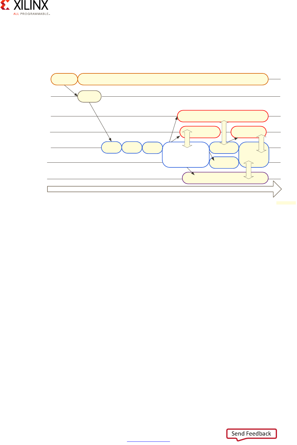
Zynq UltraScale+ MPSoC Embedded Design Methodology Guide 54
UG1228 (v1.0) March 31, 2017 www.xilinx.com
Chapter 3: System Software Considerations
Boot Process Basics
The following figure shows a simplified view of the boot process with the relevant blocks
and software:
In the boot flow image above, software systems within the PMU, CSU, and APU all work to
bring up the system. The following actions are done:
• The PMU passes control to the CSU, which checks to determine if authentication is
required.
• The CSU loads the FSBL into the on-chip memory (OCM).
• The FSBL is then executed on the APU; alternatively it can also be executed on the RPU.
• The FSBL then starts the customer’s application software or a second stage boot loader
such as U-Boot.
The following figure shows another perspective to the boot process. The PMU controls all
the power and reset sequences. The PMU releases the CSU first so that it can perform
internal checks and initializations that are usually not exposed to the user. Control goes to
either the RPU or the APU based on configuration of the boot image that starts executing
the FSBL. The FSBL loads all other components in the system such as the RTOS on the RPU,
the PL Bit Stream, ATF and U-Boot, Linux, Hypervisors, and so forth to bring up the entire
system.
X-Ref Target - Figure 3-5
Figure 3-5: Sample Boot Process
Time
Release
CSU
Power
Monitoring
Load
FSBL
AMP
Firmware
U-Boot
Linux
PMU
CSU
BootROM
RPU0
APU0 FSBL
AMP
Firmware
RPU1
AMP
Firmware
APU1,
APU2,
APU3,
...
Linux
Linux
AMP
Firmware
MB (PL)
RPMsg*
AMP Firmware
*RMPsg is provided in the Xilinx OpenAMP Library
RPMsg*
RPMsg*
RPMsg*
ATF
;
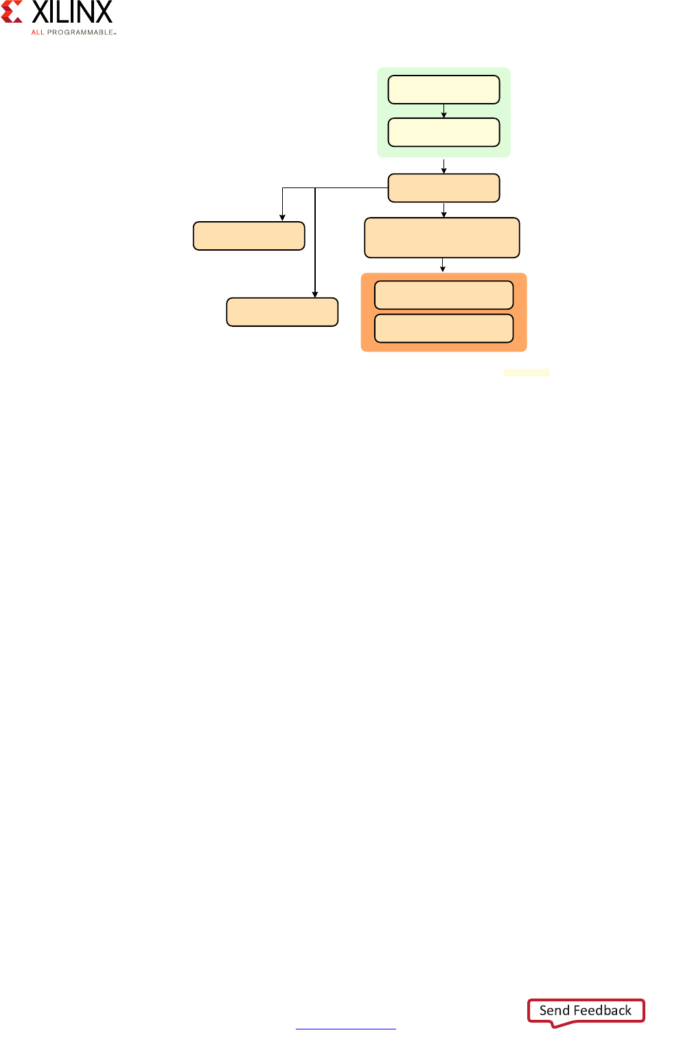
Zynq UltraScale+ MPSoC Embedded Design Methodology Guide 55
UG1228 (v1.0) March 31, 2017 www.xilinx.com
Chapter 3: System Software Considerations
Note that the PMU firmware, the CSU boot ROM and the FSBL are required in order to
ensure fundamental capabilities such as hardware root of trust, warm restart, and isolation
between subsystems. The use of the ATF also goes hand-in-hand with the use of Linux.
Secure Boot
There are two modes of booting the Zynq UltraScale+ MPSoC device: secure and
non-secure. The earlier timing diagram essentially illustrated the non-secure booting
process. Here's a more complete boot example showing secure booting:
X-Ref Target - Figure 3-6
Figure 3-6: Alternative View of Boot Process
Platform
Management ROM
Configuration
Security ROM
First Stage
Boot Loader
Loads ARM Trusted Firmware,
Loads U-Boot for Hypervisor
and non-secure OS
Loads Hypervisor on APU
Uboot loads Linux Kernel
on APU
Load RTOS on RPU
Load PL bitstream
X18661-032917
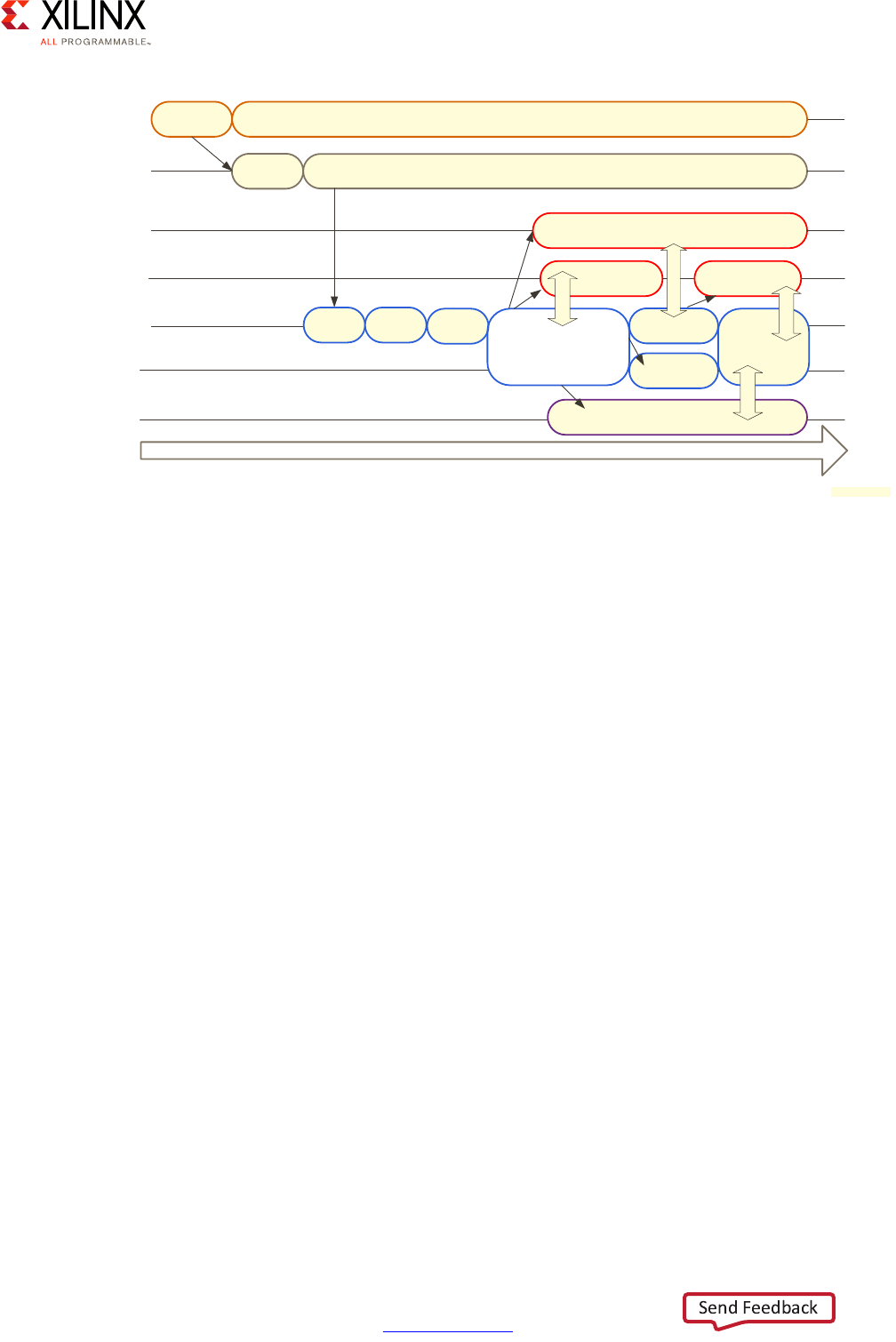
Zynq UltraScale+ MPSoC Embedded Design Methodology Guide 56
UG1228 (v1.0) March 31, 2017 www.xilinx.com
Chapter 3: System Software Considerations
In this case, the CSU does a bit more work, including the following:
• Performs an authentication check and proceeds only if the authentication check passes.
Checks the image for any encrypted partitions.
• If the CSU detects partitions are encrypted, the CSU performs decryption and loads the
FSBL into the OCM.
This example also illustrates how the Linux instance running on the APU uses OpenAMP to
kick-start software on the RPU as well as on a MicroBlaze running in the PL.
Boot Time Performance
As mentioned earlier, some operations can only be conducted during boot time. Hence,
understanding whether you have boot time constraints will help guide your customization
of the boot process. Do you have a standard to follow, say for example PCIe, CAN-FD or
Ethernet AVB, that requires your system to come online within a prescribed time limit? In
those cases, you can use partial reconfiguration where you load a core part of the bitstream
quickly during boot up and then load the rest at a later time.
X-Ref Target - Figure 3-7
Figure 3-7: Secure Boot Process
Time
Release
CSU
Power
Monitoring
Load
FSBL
Tamper
Monitoring
AMP
Firmware
U-Boot
Linux
PMU
CSU
BootROM
RPU0
APU0 FSBL
AMP
Firmware
RPU1
AMP
Firmware
APU1,
APU2,
APU3,
...
Linux
Linux
AMP
Firmware
MB (PL)
RPMsg*
AMP Firmware
*RMPsg is provided in the Xilinx OpenAMP Library
RPMsg*
RPMsg*
RPMsg*
ATF
X18662-032117

Zynq UltraScale+ MPSoC Embedded Design Methodology Guide 57
UG1228 (v1.0) March 31, 2017 www.xilinx.com
Chapter 3: System Software Considerations
Boot Devices
The Zynq UltraScale+ MPSoC device's CSU boot ROM supports the following primary boot
devices:
•Quad SPI
•NAND
• SD/MMC
• eMMC
While the CSU does not directly support booting from SATA, Ethernet, or PCI Express. A
secondary boot from these devices is possible using minimal FSBL.
Generally, your choices depend on your needs:
• If you are looking for speed, then SPI flash is the preferred choice.
• If you are looking for capacity, then eMMC is probably a better choice for systems that
do not want to burden the host with file management of Flash.
• If you have a complex storage configuration, then NAND will provide you more
flexibility. This choice is ideal for systems that require finer control of Flash for
performance reasons and have a powerful processor to run Flash management
software.
Another aspect that you might also want to keep in mind with storage is the pin count
involved in supporting the different storage devices.
Some additional notes regarding the supported boot devices:
• QSPI (Serial Flash) primary boot mode supports 4-byte addressing.
• NAND supports Open NAND Flash Interface (ONFI) version 3.1.
• SD Card supports version 3.0 of the SD Specification.
• eMMC supports embedded Multimedia card standard version 4.51.
• NOR (Parallel Flash) is not supported.
• PS JTAG is available.
• PL JTAG is limited to FSBL.
• Split JTAG Mode is limited to FSBL.
Zynq UltraScale+ MPSoC Embedded Design Methodology Guide 58
UG1228 (v1.0) March 31, 2017 www.xilinx.com
Chapter 3: System Software Considerations
Additional Resources Regarding Booting
For more information about the booting process and the details of secure vs. non-secure
booting, refer to the following:
•Zynq UltraScale+ MPSoC Technical Reference Manual (UG1085) [Ref 7]:
° Boot and Configuration
° Security
•Zynq UltraScale+ MPSoC: Software Developers Guide (UG1137) [Ref 5]:
°Programming View of Zynq UltraScale+ MPSoC Devices
°System Boot and Configuration
°Security Features
System Software Stacks
The software stacks that can be used on the APU and RPU were listed in System Software
Methodology, page 47. Let's take a closer look at some of those stacks and the relevant
recommendations about their use.
RPU Bare Metal Software Stack
The RPU Bare Metal Software Stack is composed of several layers:
• On the bottom of the stack is the Cortex R5 Standalone board support package (BSP)
Processor Layer. This layer contains a standalone BSP with processor boot code, cache,
exception handling, memory, system timer configuration, and processor function
initialization.
• On top of the Cortex R5 Standalone BSP Processor layer lies multiple single-threaded
device drivers for various hardware components including peripheral drivers as well as
the Coresight Debug driver to support debugging on the system.
• The next layer up consists of multiple libraries available to support application software
development including C library, file system library, memory, flash, secure key, power
management library and lwIP network stack library. This layer also includes an
OpenAMP library for using the Zynq UltraScale+ MPSoC device's OpenAMP framework,
described in OpenAMP Framework, page 64.
• On top of the stack can be user applications, custom libraries, and services as needed.
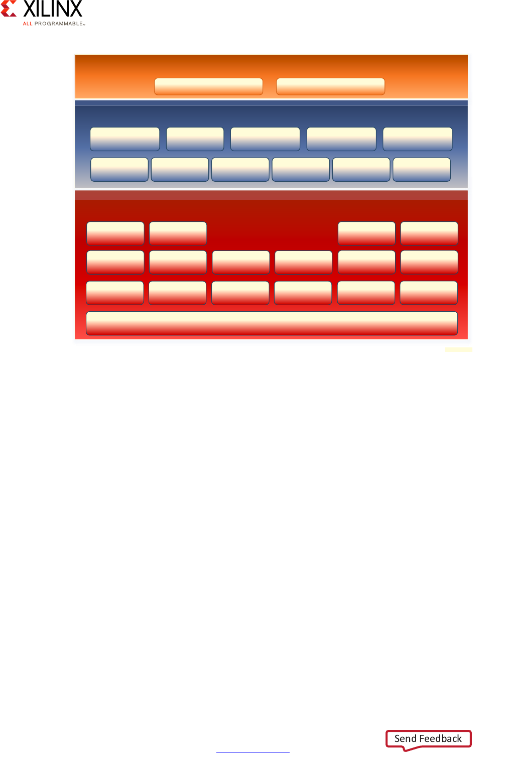
Zynq UltraScale+ MPSoC Embedded Design Methodology Guide 59
UG1228 (v1.0) March 31, 2017 www.xilinx.com
Chapter 3: System Software Considerations
While running the RPU's R5s bare metal does gives you full control over their capabilities, it
does also mean that you must manually schedule tasks, coordinate key communication
between your software components, manually managing cross-software locking, and
possibly manually take care of several other capabilities typically taken care by an OS kernel.
Running one or both of the R5s bare metal is likely best suited for applications where the
processing being done can be viewed as a limited number of well-defined or
well-synchronized tasks. If you ever see the functionality to be conducted by the R5s to
potentially expand beyond your initial plans, however, it might be best to consider using
some form of OS on the R5s. Indeed, it's not uncommon for designs that begin as single
while(1) loops to end up requiring the development of what eventually ends up being
capable OS.
X-Ref Target - Figure 3-8
Figure 3-8: RPU Bare Metal Software Stack
Standalone Kernel and Drivers
Standard USB
Drivers SysMon Driver
CoreSight
Debug Driver
EMAC Ethernet
Driver
RTC Driver Interrupt
Controller Driver
CAN Driver AXI Performance
Monitor Driver
NAND Driver QSPI Driver
SPI, I2C, UART
Drivers ZDMA Driver
GPIO Driver IPI Driver
SD Card Driver TTC Driver
Cortex R5 Standalone BSP Processor Layer
Libraries
Standard ‘C’ Library
(libXil)
Secure Key
(xilskey)
lwIP Networking
(lwip141)
Memory File System
(xilmfs)
FAT file system
(xilffs)
Serial Flash
(xilisf)
Secure
(xilsecure) RSA (xilrsa) Power Mgr API
(xilpm)
OpenAMP
(xilopenamp)
Parallel Flash
(xilflash)
Applications
Template Applications Customer Applications
;
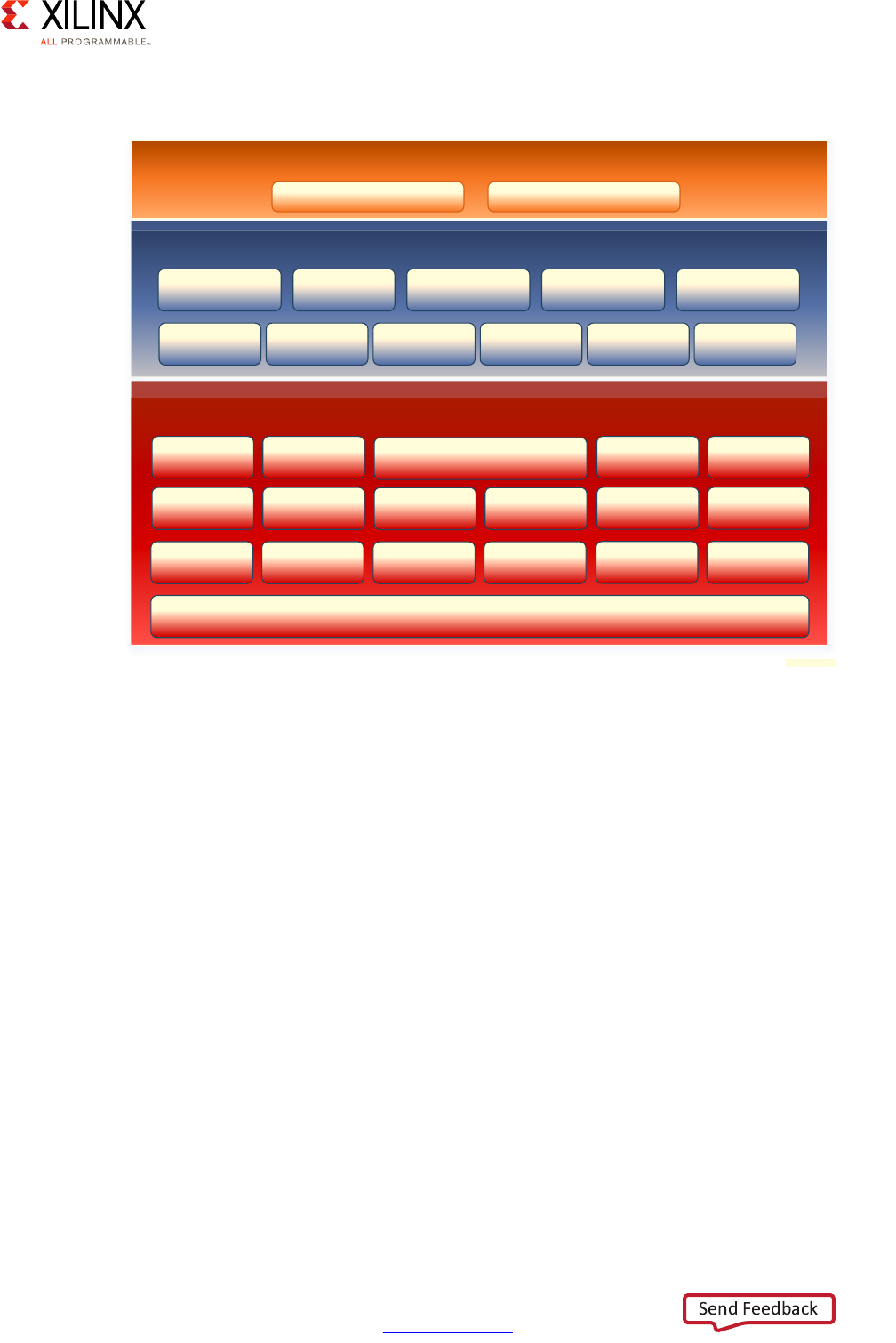
Zynq UltraScale+ MPSoC Embedded Design Methodology Guide 60
UG1228 (v1.0) March 31, 2017 www.xilinx.com
Chapter 3: System Software Considerations
RPU FreeRTOS Software Stack
APU Bare Metal Stack
The RPU FreeRTOS Software Stack is identical to the RPU Bare Metal Software Stack which
was just presented with one exception: the existence of the FreeRTOS kernel component,
which is in the bottom layer. By using FreeRTOS instead of running the RPU bare metal, you
are benefiting from an industry-standard real-time OS that will allow you to grow your
application over time without the concern of having to managing core OS functionality
yourself. On the flip side, your team will need to become accustomed to FreeRTOS and its
APIs if those aren't already familiar.
The APU's Bare Metal Software Stack consists of several layers similar to the software stacks
presented thus far:
• On the bottom of the stack is the Cortex-A53 standalone BSP, one for 32-bit mode and
one for 64-bit mode. The 32-bit mode is compatible with ARMv7-A whereas the one for
64-bit mode is compatible with ARMv8-A architecture. Each standalone BSP contains
processor boot-code, cache, exception handling, memory, system timer configuration,
and processor-specific function initialization.
X-Ref Target - Figure 3-9
Figure 3-9: FreeRTOS Software Stack
FreeRTOS Kernel and Drivers
Standard USB
Drivers SysMon Driver
CoreSight
Debug Driver
EMAC Ethernet
Driver
RTC Driver Interrupt
Controller Driver
CAN Driver AXI Performance
Monitor Driver
NAND Driver QSPI Driver
SPI, I2C, UART
Drivers ZDMA Driver
GPIO Driver IPI Driver
SD Card Driver TTC Driver
FreeRTOS 8.2.1
Cortex R5 Standalone BSP Processor Layer
Libraries
Standard ‘C’ Library
(libXil)
Secure Key
(xilskey)
lwIP Networking
(lwip141)
Memory File System
(xilmfs)
FAT file system
(xilffs)
Serial Flash
(xilisf)
Secure
(xilsecure) RSA (xilrsa) Power Mgr API
(xilpm)
OpenAMP
(xilopenamp)
Parallel Flash
(xilflash)
Applications
Template Applications Customer Applications
;
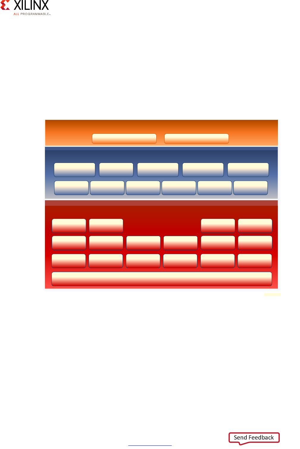
Zynq UltraScale+ MPSoC Embedded Design Methodology Guide 61
UG1228 (v1.0) March 31, 2017 www.xilinx.com
Chapter 3: System Software Considerations
• On top of the Cortex-A53 standalone BSP layer lies multiple device drivers for various
hardware components including peripheral drivers as well as the Coresight Debug
driver to support debugging on the system.
• The next layer up consists of multiple libraries available to support application software
development including standard C library, file system library, memory, flash, secure key,
power management libraries and lwIP network stack library. This layer also includes an
OpenAMP library for using the Zynq UltraScale+ MPSoC device's OpenAMP framework,
described in OpenAMP Framework, page 64.
• On top of the stack can be user applications, custom libraries, and services as needed.
The caveats regarding the bare metal use of the APU were described in Bare Metal Use of
the APU, page 50. Xilinx suggests that you review the real-time or interrupt response
requirements for your bare-metal applications to confirm whether that application can be
hosted on Xen hypervisor, which leaves additional system resources for other tasks.
X-Ref Target - Figure 3-10
Figure 3-10: APU Bare Metal Stack
Standalone Kernel and Drivers
Standard USB
Drivers SysMon Driver
CoreSight
Debug Driver
EMAC Ethernet
Driver
RTC Driver Interrupt
Controller Driver
CAN Driver AXI Performance
Monitor Driver
NAND Driver QSPI Driver
SPI, I2C, UART
Drivers ZDMA Driver
GPIO Driver IPI Driver
SD Card Driver TTC Driver
Cortex A53 Standalone BSP Processor Layer
Libraries
Standard ‘C’ Library
(libXil)
Secure Key
(xilskey)
lwIP Networking
(lwip141)
Memory File System
(xilmfs)
FAT file system
(xilffs)
Serial Flash
(xilisf)
Secure
(xilsecure) RSA (xilrsa) Power Mgr API
(xilpm)
OpenAMP
(xilopenamp)
Parallel Flash
(xilflash)
Applications
Template Applications Customer Applications
;
Zynq UltraScale+ MPSoC Embedded Design Methodology Guide 62
UG1228 (v1.0) March 31, 2017 www.xilinx.com
Chapter 3: System Software Considerations
APU Linux Software Stack
Running Linux on the APU is the preferred way of operating the Zynq UltraScale+ MPSoC
device. The APU Linux Software Stack delivered as a part of the PetaLinux tools also consists
of several layers, many of which are part of the standard Linux software ecosystem:
• On the bottom of the stack is the Linux Core Kernel and Services as well as the
Cortex-A53 BSP Processor Layer. These components provide processor boot code,
cache, exception handling, memory, system timer configuration, and processor-specific
functions initialization.
• On top of this bottom layer lie multiple device drivers, peripherals drivers, and several
Linux drivers and system services at the kernel level including resource management,
file systems, IO management, power management, network and multimedia stack
layers, graphics, video drivers, and network stacks.
• The next layer up contains multiple libraries to support application software
development standard C lib, file system lib, memory, flash, secure key, power
management lib, multimedia libraries OpenGL, EGL, DRM library, Display server, Audio
Server, OpenMAX and many other middleware libraries. This layer also includes an
OpenAMP library for using the Zynq UltraScale+ MPSoC device's OpenAMP framework,
described in OpenAMP Framework, page 64.
• On top of the stack can be user applications, custom libraries, and services as needed.
X-Ref Target - Figure 3-11
Figure 3-11: APU Linux Software Stack
Linux Kernel and Drivers
File System
Manager
RPmsg &
Remoteproc
Linux TCP/IP
Network Stack
Graphics
Driver
Ethernet
Driver
USB
Drivers
V4I2 ARM Arch
Support
SATA
Driver
Video Codec
Driver
SPI, I2C, UART
Drivers
PCIe
Driver
Display
Driver
ALSA Audio
Driver
SD Card
Driver
Flash
Drivers
Linux Core Kernel and Services
Libraries
EGL DRM Library Display Server Audio Server OpenAMP
Library Power Mgr API
Applications
Template Applications Customer Applications
OpenGL FBdev Other Middleware Libraries RSA Secure
Library OpenMAX
FileSystem
Services
File System
DRM KMS SMP
Support
Cortex A53 BSP Processor Layer
;

Zynq UltraScale+ MPSoC Embedded Design Methodology Guide 63
UG1228 (v1.0) March 31, 2017 www.xilinx.com
Chapter 3: System Software Considerations
Linux has been used in embedded systems, servers and desktops for more than 20 years
and has a very rich and active ecosystem surrounding it. It is therefore a solid foundation
for many custom and general-purpose applications, and is especially well-suited to enable
you to unlock the full potential of the APU's multi-core design. If your team is already
familiar with Linux then this will probably be the most natural path to follow. If, on the other
hand, Linux is unfamiliar territory then we recommend you start your efforts with Xilinx's
own PetaLinux. As was mentioned earlier, PetaLinux represents a low barrier-to-entry Linux
version for your embedded needs.
A potential flip side to using Linux can be its distributed development model that makes it
such that there isn't a single authoritative entity that provides all definitive information
about its uses, as can be the case of more traditional embedded OSes. Hence, if you aren't
familiar with Linux, researching information about specific aspects of the system may
require filtering out information which isn't relevant to your use-case. Then again, Linux has
been used successfully by so many teams for so many embedded projects that the latter is
likely not that much of an impediment.
A more tangible technical limitation of using Linux is that, by default, its kernel does not
provide hard-real-time capabilities. There are a few well-known real-time extensions to
Linux, namely PREEMPT_RT and Xenomai, but neither are fully part of the Linux kernel at the
time of this writing. Hence, if you intend to use such extensions, you will need to put some
effort into adding the relevant patches to your Linux kernel. As was discussed earlier,
however, if you have any real-time needs then you should first and foremost look at the
RPU and its capabilities.
The Linux variants supported by Xilinx will be discussed in more detail later in this chapter.
You can also find more information about using Linux in the Zynq UltraScale+ MPSoC:
Software Developers Guide (UG1137) [Ref 5].
When using Linux on the APU, there are a few more software stacks that must be discussed
in greater detail, namely with regards to graphics. Refer to Chapter 9, Multimedia for more
information about the following stacks in the context of Linux:
• Linux DisplayPort Stack
• Linux GPU Software Stack
• Linux Video Codec Driver Stack
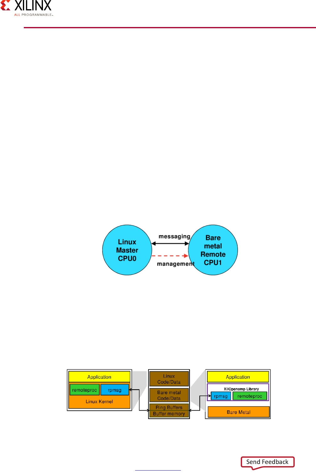
Zynq UltraScale+ MPSoC Embedded Design Methodology Guide 64
UG1228 (v1.0) March 31, 2017 www.xilinx.com
Chapter 3: System Software Considerations
OpenAMP Framework
The Open Asymmetric Multiprocessing (OpenAMP) is a layered, modular framework that
provides a common API and methodology for interconnecting software components within
Asymmetric Multi Processing (AMP) systems like the Zynq UltraScale+ MPSoC device. It
enables software applications running within such a heterogeneous multiprocessor system,
where different core instances can run different operating systems (e.g. HLOS, Bare Metal,
or real-time operating systems such as FreeRTOS), to communicate and coordinate. More
specifically, OpenAMP is a generic abstract framework that allows powering on, loading
firmware, powering off, and sharing of information (communicating) between the
heterogeneous processors that make up the system.
In AMP systems, it is common for the master processor to bring up software on remote
cores as driven by demand. The cores then communicate using Inter Processor
Communication (IPC) allowing the master processor to offload work to the other
processors.
The following figure illustrates a very simple AMP topology. In this example, Linux runs as
the master processor in the APU and the RPU runs a Bare Metal application as the remote
processor. Linux is responsible for loading and starting the remote processor.
OpenAMP consists of two key components:
•Remoteproc: A managing framework that controls the Life Cycle Management (LCM) of
the remote processors from the master processor.
•RPMsg: A messaging framework that, through an API, allows Inter Process
Communications (IPC) between software running on the independent cores in the AMP
system.
X-Ref Target - Figure 3-12
Figure 3-12: Simple AMP Topology
X-Ref Target - Figure 3-13
Figure 3-13: Remoteproc and RPMsg
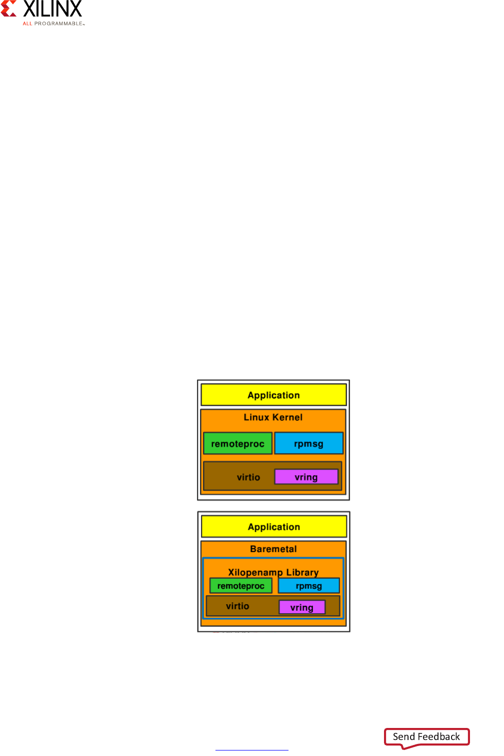
Zynq UltraScale+ MPSoC Embedded Design Methodology Guide 65
UG1228 (v1.0) March 31, 2017 www.xilinx.com
Chapter 3: System Software Considerations
Remoteproc
Remoteproc is implemented through a device driver and directed through an API. The API
can have Remoteproc instruct the master processor to load code and data into a remote
processor's memory, start the remote processor, manage a communication channel
between itself and a remote processor, and shutdown a remote processor.
From the remote processor's perspective, the call on the master processor to the API can
initialize the Remoteproc system on the remote processor, manage a communication
channel between the remote processor and the master processor, and shutdown the
Remoteproc system on the remote processor.
RPMsg
RPMsg is a messaging bus between processors where each processor is a device on the bus.
Processors have channels that are communication links between each other and are created
when the remote processor is started. The channels are identified by a name with a source
and destination address.
RPMsg uses Virtual I/O (Virtio) Component. Virtio provides Virtual I/O services to support
communication between the master processor and the remote processors.
Following is an illustration showing how Virtio fits in the OpenAMP layers:
Virtio uses vring, which is a transport abstraction for I/O operations used by Virtio. Vring
implements a ring buffer.
X-Ref Target - Figure 3-14
Figure 3-14: RPMsg with Virtio
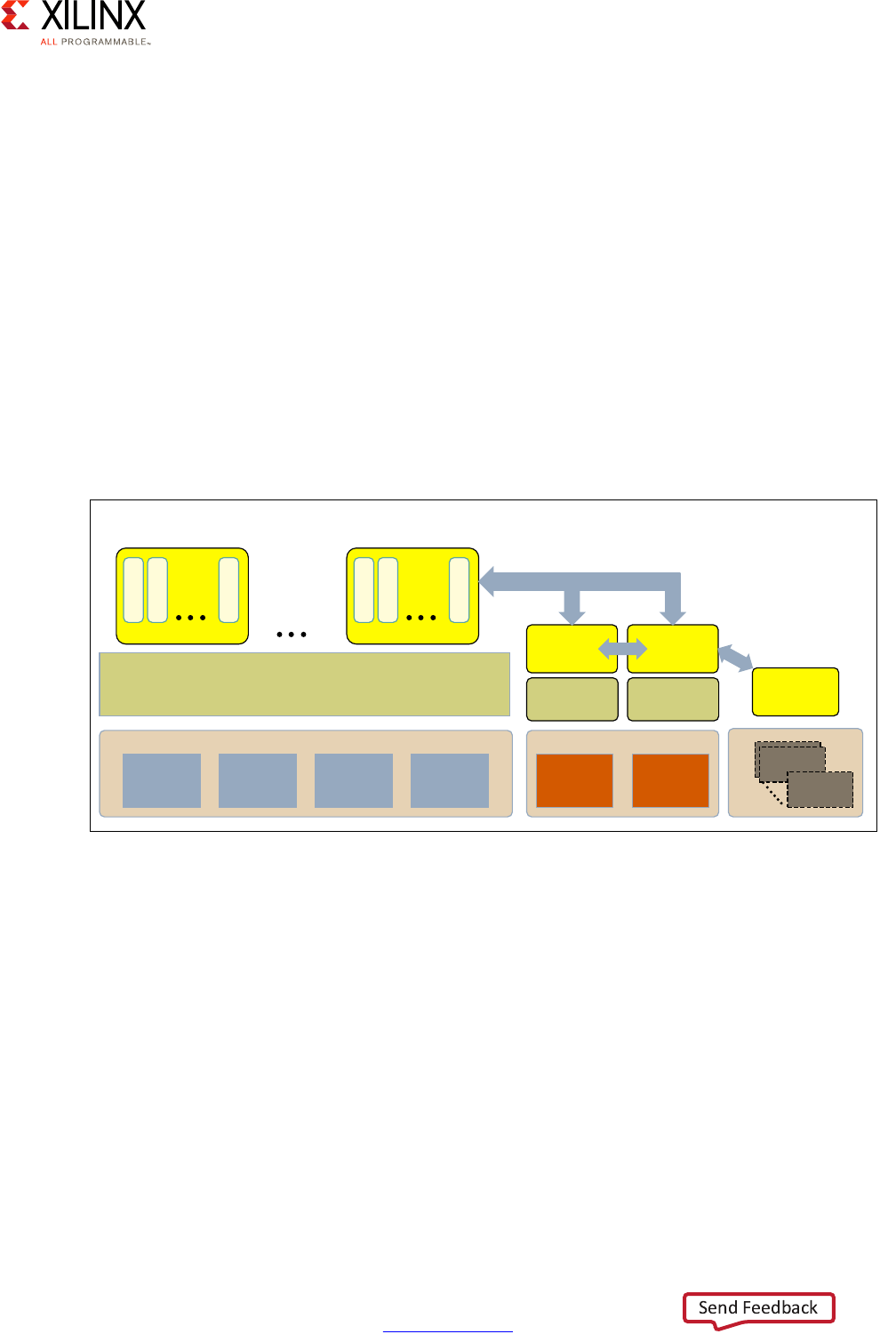
Zynq UltraScale+ MPSoC Embedded Design Methodology Guide 66
UG1228 (v1.0) March 31, 2017 www.xilinx.com
Chapter 3: System Software Considerations
API
The OpenAMP API is implemented on both the master processor and on the remote
processors. The API directs the RPMsg to do the following:
• Send messages to a default endpoint of a channel
• Send complex messages that allow for explicit source and destination addresses and
blocking options
• Create and destroy channels and channel endpoints
• Receive data
• Recognize and use buffer size during data transfers
Here's an example use of the APIs between OpenAMP-enabled cores on the Zynq
UltraScale+ MPSoC device:
Additional Resources
For more information about OpenAMP, refer to the Zynq UltraScale+ MPSoC OpenAMP:
Getting Started Guide (UG1186) [Ref 8].
X-Ref Target - Figure 3-15
Figure 3-15: Hybrid Example with SMP and AMP Using OpenAMP Framework
$38
$50
&RUWH[$
$50
&RUWH[$
$50
&RUWH[$
$50
&RUWH[$
/LQX[.HUQHOLQ603PRGH 5726
.HUQHO
%DUH0HWDO
$SSOLFDWLRQ
$SSOLFDWLRQ
7KUHDG
7KUHDG
7KUHDGQ
;
538
$50
&RUWH[5
$50
&RUWH[5
3/
0LFUR%OD]H
0LFUR%OD]H
5726
.HUQHO
%DUH0HWDO
$SSOLFDWLRQ
%DUH0HWDO
$SSOLFDWLRQ
$SSOLFDWLRQQ
7KUHDG
7KUHDG
7KUHDGQ
RPMsg
RPMsg
Open AMP
(APIs for loading/ Unloading
firmware, Message Passing)
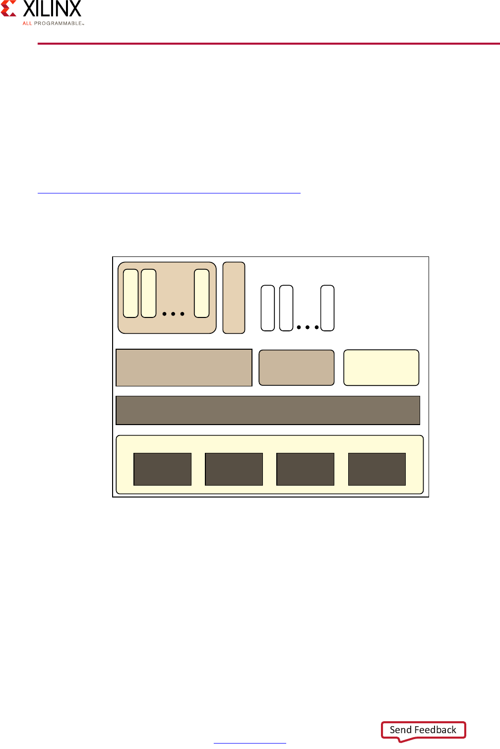
Zynq UltraScale+ MPSoC Embedded Design Methodology Guide 67
UG1228 (v1.0) March 31, 2017 www.xilinx.com
Chapter 3: System Software Considerations
Xen Hypervisor
Xilinx has ported the Xen open source hypervisor to the Xilinx Zynq UltraScale+ MPSoC
device and provides the ability to run multiple operating systems on the same computing
platform. Xen, which runs directly on the hardware, is responsible for managing CPU,
memory, and interrupts while multiple OSes can run on top of the hypervisor. These OS are
called domains; they are also sometimes called virtual machines (VMs).
Note: For additional information on the Xen Hypervisor, see Xen Project Software Overview at
https://wiki.xen.org/wiki/Xen_Project_Software_Overview.
The following figure shows an example Xen Hypervisor architecture on the Zynq
UltraScale+ MPSoC device:
The Xen hypervisor controls one domain, which is called domain 0 (or dom0), and one or
more guest domains (or domU). The control domain has special privileges, such as:
• Capability to access the hardware directly
• Ability to handle access to the I/O functions of the system
• Interaction with other virtual machines.
X-Ref Target - Figure 3-16
Figure 3-16: Xen Hypervisor Architecture
Hypervisor
APU
ARM
Cortex-A53
ARM
Cortex-A53
ARM
Cortex-A53
ARM
Cortex-A53
Linux Kernel in
SMP mode
RTOS
Kernel
Baremetal
Application
Application 1
Thread 1
Thread 2
Thread n
Application n
Task 1
Task 2
Task n
X14840-081015

Zynq UltraScale+ MPSoC Embedded Design Methodology Guide 68
UG1228 (v1.0) March 31, 2017 www.xilinx.com
Chapter 3: System Software Considerations
It also exposes a control interface to the outside world, through which the system is
controlled. Each guest domain runs its own OS and application. Guest domains are
completely isolated from the hardware.
The hypervisor is started by the bootloader; refer to Boot Process Software, page 53 for
details. Running multiple OSes using Xen hypervisor involves setting up the host OS and
adding one or more guest OS. In the case of the Zynq UltraScale+ MPSoC device, Xen can
also run bare metal applications without a guest OS.
Performance Tuning Considerations
As discussed earlier, depending on your specific real-time and interrupt response
requirements, the use of the Xen hypervisor might be appropriate for your system design
configurations. Still, every design is different and your needs may require some additional
attention to certain aspects of Xen's use. Here are some performance tuning tips for
optimizing Xen on the Zynq UltraScale+ MPSoC device.
Interrupt Response Time
Interrupt response time is the time it takes for an interrupt generated at the hardware level
to trigger the execution of the corresponding code in the OS running on that hardware.
Interrupt response times differ when comparing a native OS and a guest OS. Performance
factors for native OSes involve operations taking place at the processor's exception Level 3
(per ARMv8 architecture), the OS interrupt handler, and the timer and measurement
accuracy that is used to test the actual response time. For a guest OS, performance factors
for interrupt response times are much more complex as they must account for a number of
influential factors including hypervisor interrupt handling and routing routines, hypervisor
timer resolution, and guest OS configuration.
If, after conducting your measurements, you find that interrupt response times of guest
OSes need fine tuning for your application, you might consider the following optimizations,
which leverage relatively straightforward configuration or design changes:
• Xen hypervisor scheduler selection and configuration
• Guest OS to physical CPU assignment
• Guest OS: Device polling as compared to interrupt driven decisions
Additional optimization techniques are possible, but these are beyond the scope of this
document.

Zynq UltraScale+ MPSoC Embedded Design Methodology Guide 69
UG1228 (v1.0) March 31, 2017 www.xilinx.com
Chapter 3: System Software Considerations
Boot Time
Boot time is the measurement of time required by the Xen hypervisor and Xen Dom0 to get
to the point where it is ready to boot the first guest OS. Boot time depends on the
execution time of FSBL, ARM Trusted Firmware, and U-Boot. Further dependencies exist on
the boot device and secure boot flow (e.g. Xen Hypervisor start-up and Dom0 start-up).
If you find that boot time is an issue for your use case, you can consider several things that
do not require modification of the hypervisor itself:
• Dom0 configuration (smaller, faster)
• Boot device selection (applies to systems without hypervisors)
• Secure boot parameters (applies to systems without hypervisors)
I/O Throughput of Pass Through Devices
The Zynq UltraScale+ MPSoC includes an IOMMU (ARM SMMU-400) which, when
supported by a hypervisor such as Xen, allows a guest OS to use its native DMA-capable
device driver, and the device to directly pass data through to the guest without intervening
layers of emulation or virtualization.
The I/O throughput in such a configuration is dependent on the performance of the device
driver as deployed on the same OS with some small penalty to perform the second stage
address translation provided by the SMMU.
I/O Throughput of Paravirtualized Shared Devices
Xen hypervisor supports an infrastructure for paravirtualized devices which enables two key
features:
• Devices that are owned and controlled by Xen Dom0 can be effectively shared among
multiple guest OSes.
• Guest OSes can communicate between themselves using virtual devices that present
themselves to each OS as UARTs or network interfaces.
The I/O throughput in this kind of configuration is dependent on the following factors:
• Performance of the native Linux device driver (used by Dom0)
• IO Device Bandwidth required by other guest OSes
• Performance of the Xen-bus infrastructure
• Workload of Xen Dom0 and Xen DomU(s)
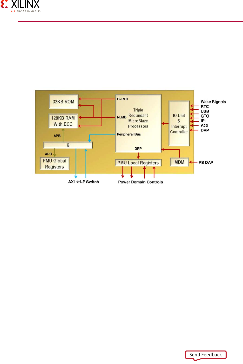
Zynq UltraScale+ MPSoC Embedded Design Methodology Guide 70
UG1228 (v1.0) March 31, 2017 www.xilinx.com
Chapter 3: System Software Considerations
PMU Software
The Platform Management Unit (PMU) has many roles, including participating in the boot
process, providing power management APIs and handling various system errors. This
section covers some of the software development aspects related to the PMU. More details
about the power management specifics are described in Platform Management Unit,
page 93. The PMU functional block diagram is as follows:
Memory
The PMU uses the following memory types:
• RAM has error-correcting code (ECC) memory for data and has optional user/firmware
code.
• PMU ROM has a default Interrupt Service Handler (ISR), which is used in Hook Mode for
interrupt handling.
• PMU Memory (ROM and RAM) handles Power Management functions (e.g. Power Up,
Power Down, IPI, Reset Requests.)
• PMU has a user-code area in a Xilinx-provided framework that gets loaded into the
PMU RAM.
Note that the amount of memory available for extending the PMU's functionality is very
limited. Doing power management in Linux, such as frequency scaling, affects the size of the
PMU firmware. Hence, you need to carefully assess your power management needs in order
to ensure that the required functionality will fit in the PMU's memory.
X-Ref Target - Figure 3-17
Figure 3-17: PMU Block Diagram
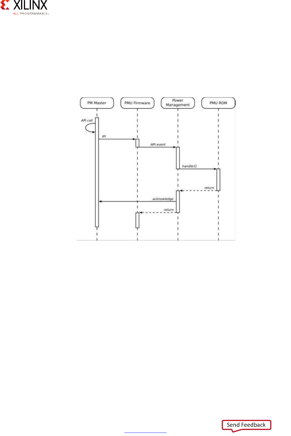
Zynq UltraScale+ MPSoC Embedded Design Methodology Guide 71
UG1228 (v1.0) March 31, 2017 www.xilinx.com
Chapter 3: System Software Considerations
Power Management Framework
The power management software framework supports multiple power reduction modes
(called Power Domains) that are targeted for various hardware and use applications that
have robust and custom power needs. The framework is provided as source code and thus
is customizable. The following figure illustrates how a typical framework call propagates
through the system:
The framework consists of different API layers viewed left to right in the previous figure. To
see how the framework supports power actions, consider a master power unit such as a
Core A53 unit interrupting the PMU via an Inter-Processor Interrupt (IPI) to perform some
power action such as shutting down a power island. The PMU Firmware receives the IPI and
then generates an API event that results in a handler call to ROM where the default
Interrupt Service Routine (ISR) resides and would perform the power action. After the action
is handled (e.g. the power island is shut down), the code returns and acknowledge signals
work their way back through the framework completing the request.
The PMU Framework run-time software supports enabling the system power-down modes,
manages the power-down modes and wakes up the system as needed, maintains the proper
system power state, and acts as a delegate to both the APU and RPU when they are in a
sleep state and need to be woke up.
Within the framework, the PMU is the Power Management Server. The server provides an
API to all masters, controls the external power management ICs and all power domain
X-Ref Target - Figure 3-18
Figure 3-18: Power Management Cell Sequence
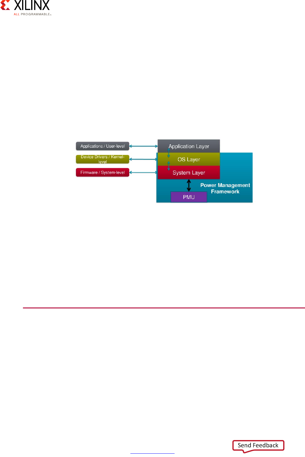
Zynq UltraScale+ MPSoC Embedded Design Methodology Guide 72
UG1228 (v1.0) March 31, 2017 www.xilinx.com
Chapter 3: System Software Considerations
switches, finalizes subsystem suspension, and can wake up suspended subsystems as
needed.
Processing units (APU and RPU) are Power Management Masters. The masters can request
various device power switching from the Power Management Server, initiate and perform
subsystem suspension, perform subsystem resume when told to wake up, and respond to
requests from the PMU.
The following figure shows the software layers within and on top of the PMU Framework.
These layers allow for different levels of power management access for applications and
low-level firmware. Complex processing unit software stacks will use all layers, while
simpler units (e.g. Bare Metal) use just the system level API:
All the work through the framework and the layers is facilitated through the power
management API, which manages the following:
• System level functions for suspending Processing Units
• System level functions for managing Power Management Slaves
• Miscellaneous system level functions
• Direct control system functions (reads and writes)
Software Development Tools
Xilinx provides a wide range of software development tools to enable you to effectively
leverage every aspect of the Zynq UltraScale+ MPSoC device to your design's benefit. This
section overviews these tools and how they fit into the Zynq UltraScale+ MPSoC device's
rich software capabilities.
X-Ref Target - Figure 3-19
Figure 3-19: Power Management Framework

Zynq UltraScale+ MPSoC Embedded Design Methodology Guide 73
UG1228 (v1.0) March 31, 2017 www.xilinx.com
Chapter 3: System Software Considerations
Development Environments and Kits
The following diagram shows the primary development environments you can use to
develop solutions designed to run on the Zynq UltraScale+ MPSoC devices.
Vivado Design Suite
This integrated development environment (IDE) is industry's first SOC-strength design suite
suited for designing hardware solutions. Vivado® includes a High Level Synthesis (HLS)
compiler that is used to convert C-based algorithms to hardware IP (Vivado HLS) and a
block-based IP integration tool that lets you integrate IP from a large Xilinx IP library. For
system verification, Vivado includes the Vivado Logic Simulator, a mixed-language
simulation tool that includes a logic analyzer for system debugging on the target
environment (Vivado Logic Analyzer). You can even extend Vivado functionality through the
tool command language (Tcl), which is the underlying scripting language used throughout
Vivado.
PetaLinux
PetaLinux is a full Embedded Linux System Development Kit. The Kit includes the Linux OS
and a complete configuration, build, and deployment environment for Xilinx silicon; Linux
OS configuration; command-line tools; development templates (application, device driver,
and library); debug agents; GCC tools; an integrated QuickEMUlator (QEMU) emulator; and
Xilinx BSP packages.
X-Ref Target - Figure 3-20
Figure 3-20: Xilinx Development Environments for the Zynq UltraScale+ MPSoC Device

Zynq UltraScale+ MPSoC Embedded Design Methodology Guide 74
UG1228 (v1.0) March 31, 2017 www.xilinx.com
Chapter 3: System Software Considerations
PetaLinux pulls together components such as the Linux kernel, U-Boot, project-specific
components, and project-specific libraries. Components are not necessarily C code but can
be a series of instructions for accomplishing something in a PetaLinux project. PetaLinux
configuration utilities allow you to enable or disable specific components.
Because everything is component-based in PetaLinux, modularity becomes a key strength
for designing using this kit. With libraries of different components, a developer can easily
design for variations by iterating on previous designs.
PetaLinux uses make in the background to build a project.
As mentioned earlier, if you are just looking for a basic scheduler or operating system for
operating the APU's A53s but aren't very familiar with Linux, PetaLinux is likely a great
starting point.
Xilinx Software Development Kit
The Xilinx Software Development Kit (SDK) is also an Integrated Design Environment (IDE)
for creating embedded applications on any Xilinx processor including the MicroBlaze soft
processor. It supports complete development and debugging of software and can be
included with the Vivado Design Suite as well as function as a stand-alone interface. The
SDK is based on the popular Eclipse IDE.
SDK interfaces with the Vivado hardware design environment such that Vivado can export
the designed hardware to the SDK to automatically create the software environment
required for that design, including BSP packages and drivers.
The SDK is bundled with an editor, compilers, build tools, flash memory management,
debugging and profiling tools. SDK supports JTAG debugging through a single JTAG cable.
SDSoC Development Environment
The SDSoC™ Development Environment provides a familiar embedded C/C++/OpenCL
application development experience that includes an Eclipse IDE and a comprehensive
design environment for heterogeneous Zynq UltraScale+ MPSoC deployment. The
development environment uses a C/C++/OpenCL full-system optimizing compiler, delivers
system level profiling, includes automated software acceleration in Programmable Logic
(PL), includes automated system connectivity generation, and includes libraries to speed up
programming. The SDSoC development environment also enables end user and third party
platform developers to rapidly define, integrate, and verify system level solutions and
enable their end customers with a customized programming environment.
Zynq UltraScale+ MPSoC Embedded Design Methodology Guide 75
UG1228 (v1.0) March 31, 2017 www.xilinx.com
Chapter 3: System Software Considerations
The development environment does the following:
• Includes an easy-to-use Eclipse IDE to develop a full Zynq All Programmable SoC and
MPSoC system with embedded C/C++/OpenCL applications
• Accelerates functions in PL
• Supports bare metal, Linux, and FreeRTOS as target operating systems
• Provides Xilinx libraries as part of Vivado HLS and provides optional hardware
optimized libraries available from Alliance Members
You can learn more about the SDSoC Development System at
https://www.xilinx.com/products/design-tools/software-zone/sdsoc.html.
Developer Flow
Developers are not limited to one environment when creating software solutions. On the
contrary, multiple environments are used to create single images. For example, an
executable flash image for the Zynq UltraScale+ MPSoC can be created by multiple tools:
• The Vivado IP integrator and Processor Configuration Wizard (PCW) configure the PS
subsystem and the .bit file component.
• The SDK is used to create the BSPs, PMU Firmware, FSBL, and application images, and
includes the bootgen utility for creating the combined images.
• PetaLinux is used to create the Open Source software images such as U-Boot, ATF,
Linux, device tree blobs, and so forth.
The following are two design flows that show multiple development environments and
tools. The first example is for developing a Bare Metal image and employs both Vivado and
the SDK.
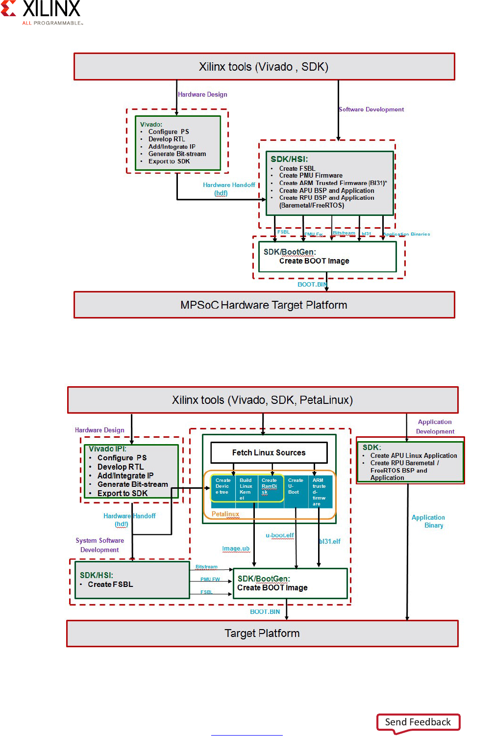
Zynq UltraScale+ MPSoC Embedded Design Methodology Guide 76
UG1228 (v1.0) March 31, 2017 www.xilinx.com
Chapter 3: System Software Considerations
This next example uses all three development environments to produce a Linux image:
X-Ref Target - Figure 3-21
Figure 3-21: Bare Metal Image Generation
X-Ref Target - Figure 3-22
Figure 3-22: Linux Image Generation

Zynq UltraScale+ MPSoC Embedded Design Methodology Guide 77
UG1228 (v1.0) March 31, 2017 www.xilinx.com
Chapter 3: System Software Considerations
Yocto Project Development
If your team is already familiar with Linux and you would like to take full control of your
Linux enablement then Yocto is an appropriate choice than PetaLinux. Yocto recipes for the
Zynq UltraScale+ MPSoC device for use with the Yocto Project tools and development
environment are available on Xilinx's git servers.
Yocto features include:
• Provides a recent Linux Kernel along with a set of system commands and libraries
suitable for the embedded environment.
• Makes available system components such as X11, GTK+, Qt, Clutter, and SDL (among
others) so you can create a rich user experience on devices that have display hardware.
For devices that do not have a display or where you wish to use alternative UI
frameworks, these components need not be installed.
• Creates a focused and stable core compatible with the OpenEmbedded project with
which you can easily and reliably build and develop Linux software.
• Supports a wide range of hardware and device emulation through the quick emulator
(QEMU).
The following figure illustrates the Yocto Project development environment:
Note that as of 2016.4 the PetaLinux development environment presented earlier has a full
Yocto back end.
X-Ref Target - Figure 3-23
Figure 3-23: Yocto Project Development Environment
User Configuration
Metadata
(.bb+patches)
Machine(BSP)
Configuration
Policy Configuration
Source
Fetching
Patch
Application
Configuration /
Compile /
Autoreconf as
needed
Output
Analysis for
package
splitting plus
Package
relationships
.rpm
Generation
.deb
Generation
.ipk
Generation
QA
Tests
image
Generation
Images
Application
Development
SDK
Package Feeds
Source Mirror(s)
Upstream
Project
Releases
Local
Projects
SCMs
(optional)
Upstram Source
Metadata/Inputs
Build System
Output Packages
Process steps (Tasks)
Output Image Data
SDK
Generation
X14841-020717

Zynq UltraScale+ MPSoC Embedded Design Methodology Guide 78
UG1228 (v1.0) March 31, 2017 www.xilinx.com
Chapter 3: System Software Considerations
More information about using Yocto with the Zynq UltraScale+ MPSoC device can be found
in the Zynq UltraScale+ MPSoC: Software Developers Guide (UG1137) [Ref 5].
Multimedia Development Tools
The following is available for multimedia development:
• Developers can use the PetaLinux toolchain to compile user mode libraries and kernel
mode drivers for display, audio, GPU, and the video Codec.
• Developers can use the GDB debugger or the SDK debugging tool to debug application
code in multimedia applications.
• Within the SDK, System Performance Analysis (SPA) can be used to profile a multimedia
design.
• The SDSoC development environment can generate IP given C/C++ logic and leverage
the Vivado Design Suite to generate an FPGA bitstream for an application-specific
image processing system on a chip. Refer to the SDSoC Environment User Guide: An
Introduction to the SDSoC Environment (UG1028) [Ref 9] for a demonstration.
• ARM Mali developer tools help with graphics application development.
Debugging
Debugging provides functional verification of a system, software evaluation, can detect
difficult and costly design errors early in the design process, can simulate conditions not
easily reproduced in the silicon, and can emulate the ARM A53 and R5 Cores as well as the
PS peripherals.
As mentioned earlier in this section, the IDEs provide several debugging tools and methods.
Along with debuggers that are bundled with the IDEs, other debugging tools exist:
• The Xilinx SDK supports the Xilinx System Debugger (XSDB). XSDB supports all the
common debug features such as setting breakpoints or watchpoints, stepping through
program execution, viewing the program variables and stack, and viewing the contents
of the memory in the system. It can also simultaneously debug programs running on
different processors (in a multiprocessor system), all from within the same debug
environment. For example, System Debugger can display both the cores in the APU and
multiple MicroBlaze soft-processors in the same debug session, through a single JTAG
cable.
The XSDB uses the same Xilinx hardware server that the Vivado Logic Analyzer uses as
the underlying debug engine. This is very important as it enables you to conduct
heterogeneous debugging or, in other words, debug software and hardware
simultaneously.

Zynq UltraScale+ MPSoC Embedded Design Methodology Guide 79
UG1228 (v1.0) March 31, 2017 www.xilinx.com
Chapter 3: System Software Considerations
To debug an application using XSDB, you must use an Executable Linkable Format (ELF)
file compiled for debugging in order to get debug symbols. You must also create a
debug session, including the executable name, processor target to run, and other
information. After launching the debugger, you can switch to debug perspective in the
GUI. This helps you to manage debugging and running the program.
• PetaLinux employs QEMU, Oprofile, and GDB, the GNU Debugger, as debug tools.
• Yocto Project debug tools include Perf, Ftrace, Oprofile, Sysprof, and Blktrace.
• ARM's DS-5 Development Studio employs the DS-5 Debugger. This debugger assists in
device bring-up through application debug. You can use the DS-5 Debugger to develop
code on an RTL simulator, virtual platform, and hardware.
• Some commercial Linux distributions support tools for debug.
• Zynq UltraScale+ MPSoC also supports Built-in Startup Tests (BIST), which include both
memory (MBIST) and logic (LBIST) tests.
Zynq UltraScale+ MPSoC Embedded Design Methodology Guide 80
UG1228 (v1.0) March 31, 2017 www.xilinx.com
Chapter 4
Power Considerations
Today's technology marketplace demands increasingly complex solutions and computing
functionality. Increased complexity and functionality necessitate increased power
requirements to function optimally. This puts the burden of enabling power reduction on
the system designers, architects, and engineers. This chapter covers the power
management capabilities of the Zynq® UltraScale+™ device and the recommendations
related to their usage.
Defining Your Power Needs
The Zynq UltraScale+ device has a very rich set of power management capabilities that can
be tuned to match specific power management needs. It is therefore important to take a
step back and critically analyze your system's specific design requirements in order to best
translate them into design decisions as applied to the Zynq UltraScale+ device.
Specifically, answering the following questions will help mapping your system's power
management needs to the Zynq UltraScale+ device:
1. Does the system need to do processing at all times?
2. Which parts of the Zynq UltraScale+ device can be left turned off?
3. Are there specific resume time requirements in the design?
4. Can part of your system's processing be offloaded to the Programmable Logic (PL)?

Zynq UltraScale+ MPSoC Embedded Design Methodology Guide 81
UG1228 (v1.0) March 31, 2017 www.xilinx.com
Chapter 4: Power Considerations
Power Tuning Methodology
There are five main techniques to tune your system's power management on the Zynq
UltraScale+ device:
1. Feature Disabling
2. Dynamic Power Management
3. Frequency Scaling
4. Clock Gating
5. Use of PL Acceleration
The first four techniques are common to the field of embedded systems power
management, with the Zynq UltraScale+ device providing its own specific capabilities in
these areas. In addition to these techniques, the Zynq UltraScale+ MPSoC device also
enables designers to move software tasks to programmable logic via C to HDL tools. This
offloading of software tasks to co-processors has demonstrated not only higher
performance processing, but also higher performance per watt.
To effectively tune the Zynq UltraScale+ device, we must first cover its power management
basics. The Zynq UltraScale+ MPSoC device is composed of four power domains for
efficient power management, as shown in Figure 4-1, page 82. Each power domain receives
power from external power regulators. If individual power domain control is not required,
power rails can be shared between domains.
The processing system has three main power domains: the battery-power domain, the
low-power domain, and the full-power domain. Within the low-power domain and the
full-power domain, there are additional IP power-gating options.
An additional fourth power domain is the programmable logic (PL). Power management
control is done through the platform management unit (PMU), a triple-redundant
microcontroller enabling reliable power management control.
Zynq UltraScale+ MPSoC Embedded Design Methodology Guide 82
UG1228 (v1.0) March 31, 2017 www.xilinx.com
Chapter 4: Power Considerations
Generally speaking, the higher your needs are on the power vector, the more time you
should spend studying the power management capabilities of the Zynq UltraScale+ MPSoC
device, contrast those to your designs requirements, and fine tune your implementation
accordingly. See Vector Methodology, page 9 for more information about design vectors
and how to use them.
Feature Disabling
The Zynq UltraScale+ device is feature rich and your design might not require all its
features. A first step in tuning the Zynq UltraScale+ device for your power needs is to go
through the Zynq UltraScale+ device capabilities and determine which ones are not needed
for your design. Then, you should consider the explanations in the rest of this chapter and
the related Zynq UltraScale+ device technical documentation to understand how to disable
or minimize the powering on of blocks that you do not need.
Say, for instance, that you do not need the real-time processing capabilities offered by the
R5 processors. In that case, you can configure the Zynq UltraScale+ device to disable those
processors. The same goes for the A53; you can disable those selectively. In addition to
computational blocks, you can also disable peripheral blocks such as the USB capabilities.
The higher you consider your needs to be on the power vector, the more time and care you
should spend on trimming as many features as possible from the Zynq UltraScale+ device
and disabling them using its power management capabilities.
The following sections describe power domains and power islands in detail.
X-Ref Target - Figure 4-1Zy
Figure 4-1: Zynq UltraScale+ MPSoC Power Domains
Text
Full-Power
Domain
Text
Text
Low-Power
Domain
PL Domain
Application
Processing Unit
Real-Time
Processing Unit
T
ext
n
Programmable Logic
Te
xt
DDR
Controller
Graphics Processing
Unit
High-Speed
Connectivity
Te
xt
Security &
Configuration
Unit
Platform
Management
Unit
System
Monitor
General
Connectivity
Text
Battery
Power Domain
T
Te
t
xt
BBRAM RTC
Processing System
;

Zynq UltraScale+ MPSoC Embedded Design Methodology Guide 83
UG1228 (v1.0) March 31, 2017 www.xilinx.com
Chapter 4: Power Considerations
Dynamic Power Management
After you have identified unwanted features to be disabled, the next step is to identify
which parts of the Zynq UltraScale+ device can be periodically turned off in your design. In
the most simplistic scenario of dynamic power management, no part of the Zynq
UltraScale+ device would be entirely turned off at any point in time in your design. In that
case, you might want to skip to the frequency scaling and clock discussions below. In most
cases, however, there are usually opportunities for periodically shutting down of some
components and waking them up on demand.
In one example, your design might only need the programmable logic to be active at all
times, whereas the auxiliary processor unit (APU) is only required to be on every so often. In
that case, you need to carefully consider the capabilities of the Zynq UltraScale+ device and
understand how to keep the PL on at all time, and only wake the APU when necessary.
There are many more examples. Perhaps you are able to shut the PL every so often. Perhaps
your needs are a bit more complex. For instance, say that you need the PL to be on at all
times, and, in addition to the need for temporarily waking up the APU, you also need the
real-time processor unit (RPU) to be active every given period of time.
The rest of this chapter describes how to gate the Zynq UltraScale+ device' capabilities as a
function of the dynamic power management requirements for each part of your design.
Once you have determined that you can periodically power off parts of the Zynq
UltraScale+ device, you also must consider the time it takes for these parts to wake up and
resume their operations. Bringing back a full-fledged OS such as Linux, for instance, on the
A53 is likely going to take significantly longer than bringing back the PL on-line. It is
possible that the resume time of the OS and application on the A53 might be too long for
your design and you might therefore need to move part of your logic to the PL in order to
achieve the desired response times on wakeup.
Determining resume times ahead of time can be a complex task and you might need to
prototype some parts of the basic functionality of your design in order to quantify
approximate resume times. If you are running Linux on the A53, for instance, it is likely that
the Linux resume time will be dependent on your specific software configuration and the
drivers you are using. So although Linux can be made to resume within a few hundred
milliseconds, its exact resume time cannot be predicted ahead of time for all Zynq
UltraScale+ device-based designs.
In some specific cases, careful resume time analysis might lead to the conclusion that your
design might not afford the use of dynamic power management. In those cases, you might
want to look at frequency scaling and clock gating as other means to optimize your power
management.

Zynq UltraScale+ MPSoC Embedded Design Methodology Guide 84
UG1228 (v1.0) March 31, 2017 www.xilinx.com
Chapter 4: Power Considerations
Frequency Scaling
After you have identified the parts of the Zynq UltraScale+ device that can be turned off
permanently or periodically, there are likely opportunities to further reduce the power
consumption of active parts by using frequency scaling. Although your design might
require the A53s to be active during certain periods, there might be opportunities within
those periods to further diminish the power consumption of the A53s by reducing their
speed while their full processing capabilities are not necessary.
The processing system provides power/performance scaling using two main levels of
processing systems: the APUs and the RPUs, each with its own power management
capabilities. Typically, the frequency scaling of the APU is controlled by the Linux CPU
governors.
When you scale down the processing components' frequencies, you trade better power
performance for a decrease in performance. If your design doesn't allow for such a trade off,
then the likely only remaining options to consider for your design are feature disabling (see
Feature Disabling, page 82) and clock gating, described next.
For more information about frequency scaling, see this link in the Zynq UltraScale+ MPSoC
Technical Reference Manual (UG1085) [Ref 7].
Clock Gating
Another Zynq UltraScale+ device capability at your disposal for power tuning is clock
gating. This allows disabling the clock to certain components, thereby reducing their
dynamic power usage. So while their static power usage remains unchanged—in other
words, they remain powered on—they no longer receive clock signals.
Several components of the Zynq UltraScale+ device can be clock-gated. This includes
processor cores, processor peripherals, and PL soft and hard cores.
For more information about clock gating, see this link in the Zynq UltraScale+ MPSoC
Technical Reference Manual (UG1085) [Ref 7].
Use of PL Acceleration
Unlike ASSPs, the Zynq UltraScale+ MPSoC has the unique ability to move software tasks to
the programmable logic, enabling dramatic software acceleration and higher performance
per watt. The latest generation programmable logic provides its own power reduction and
management capabilities via next-generation lower power hard IP and enhanced
performance soft IP.
The features open up entire new avenues for tuning the power usage of your embedded
systems. Indeed, unlike many of the other tuning approaches discussed above, this unique
feature of the Zynq UltraScale+ device is the only avenue that increases your system's
overall performance while still reducing your power consumption. Therefore, Xilinx strongly
Zynq UltraScale+ MPSoC Embedded Design Methodology Guide 85
UG1228 (v1.0) March 31, 2017 www.xilinx.com
Chapter 4: Power Considerations
recommends that you review your system's goals and determine which capabilities can be
implemented in the PL.
Hardware Considerations
Some of the power management features of the Zynq UltraScale+ device require board
support. Being able to power down the Full Power Domain, for example, depends on board
level support. Regulators need to be wired up correctly, through GPIO or PMBUS for
example, so that software can control them. Depending on the desired flexibility, there
might be some constraints in what power rails can be combined, thereby imposing
trade-offs with regards to simplicity of the supply design and BOM cost. Hence, care must
be given during board design to take into account the desired run-time PM features.
Software Considerations
Xilinx provides a software power management framework to support power reduction
modes. This framework is built on top of industry standards to support power modes and
submodes and is controlled through the Platform Management Unit (PMU). This power
management framework enables any system software to control power management,
including bare metal operation, traditional Linux power management as well as custom
proprietary software stacks. Example code demonstrating the use of these modes via Linux
is available.
Summary
The following table summarizes the impact each tunable capability has on performance,
power, and PL footprint.
Ultimately, power tuning typically involves making trade-offs between power consumption,
performance and available functionality.
Capacity Performance Power PL Footprint
Feature Disabling Y Y N
Dynamic Power
Management Y Y N
Frequency Scaling Y Y N
Clock Gating N Y N
Use of PL Acceleration Y Y Y
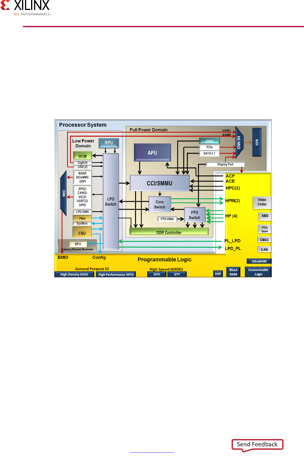
Zynq UltraScale+ MPSoC Embedded Design Methodology Guide 86
UG1228 (v1.0) March 31, 2017 www.xilinx.com
Chapter 4: Power Considerations
Four Major Power Domains
The Zynq UltraScale+ device's four major power domains were introduced earlier at a fairly
high level. The following diagram further details the components that make up these
domains. In the lower left corner is the Battery Power Domain, the upper left corner is the
Low Power Domain including the Real-Time Processing Unit (RPU). The upper right is the
Full Power Domain which includes the Application Processor Unit (APU). Finally, along the
bottom is the Programmable Logic (PL) Power Domain:
Processing System (PS) Power Domains
The Processing System (PS) operates in three power consumption modes: Battery Power
Mode, Low Power Mode, and Full Power Mode.
Battery Power Mode is the lowest power mode and simplest. It's used to keep alive a
Real-Time Clock and the battery backed RAM. Power consumption ranges from 180
nanowatts when you're powering the battery backed RAM to only 3 microwatts when the
Real-Time Clock is enabled.
Low Power Mode is associated with the Real-Time Processor Unit, or RPU. Depending on
activity level power consumption can range anywhere from approximately 20 milliwatts to
220 milliwatts.
X-Ref Target - Figure 4-2
Figure 4-2: Zynq UltraScale+ Device: Four Major Power Domains

Zynq UltraScale+ MPSoC Embedded Design Methodology Guide 87
UG1228 (v1.0) March 31, 2017 www.xilinx.com
Chapter 4: Power Considerations
The Full Power Mode is associated with the Application Processor Unit being enabled.
Depending on activity power consumption can range up to a few watts. Switching from the
Lower Power Mode to the Full Power Mode typically involves either booting or resuming the
OS, generally Linux, running on the APU.
From the feature disabling and dynamic power management perspective, the above
diagram should help you understand your trade offs in terms of processing capabilities vs
power consumption with regards to the PS power domains. Note that each mode layered on
top of another assumes the lower mode is active. In other words, being in the Full Power
Mode assumes that both the Lower Power Mode and the Battery Power Mode are active.
To illustrate processing capabilities vs power consumption trade offs, let's say the activation
of the full power mode for a specific task does not match your power budget for that
specific task. In that case, it might be worth considering moving the associated
functionality into the PL instead. If, on the other hand, the consumption is within your
accepted power budget then understanding your power consumption within the Full Power
Mode will enable you to better characterize your system's overall power usage.
Alternatively, if the consumption of the Full Power Mode is too high and yet you still need
that mode to be active, it might be worth considering using a combination of frequency
scaling and clock gating to further tune your system's power consumption.
From a resume time requirements perspective, you will need to consider how much time it
takes for switching between power modes. If, for example, your resume time is critical and
must be as minimal as possible and you need to switch from battery power mode to full
power mode to process important input, you will want to make sure that such switching
time matches your needs. Say you are running Linux on the APU, for instance, and a
user-space process is the proposed method for dealing with specific input. In that case,
you'll want to make sure that the time delta between the external event and the resumption
of said user-space process fits your requirements.
X-Ref Target - Figure 4-3
Figure 4-3: Processing System: Multiple Power Modes
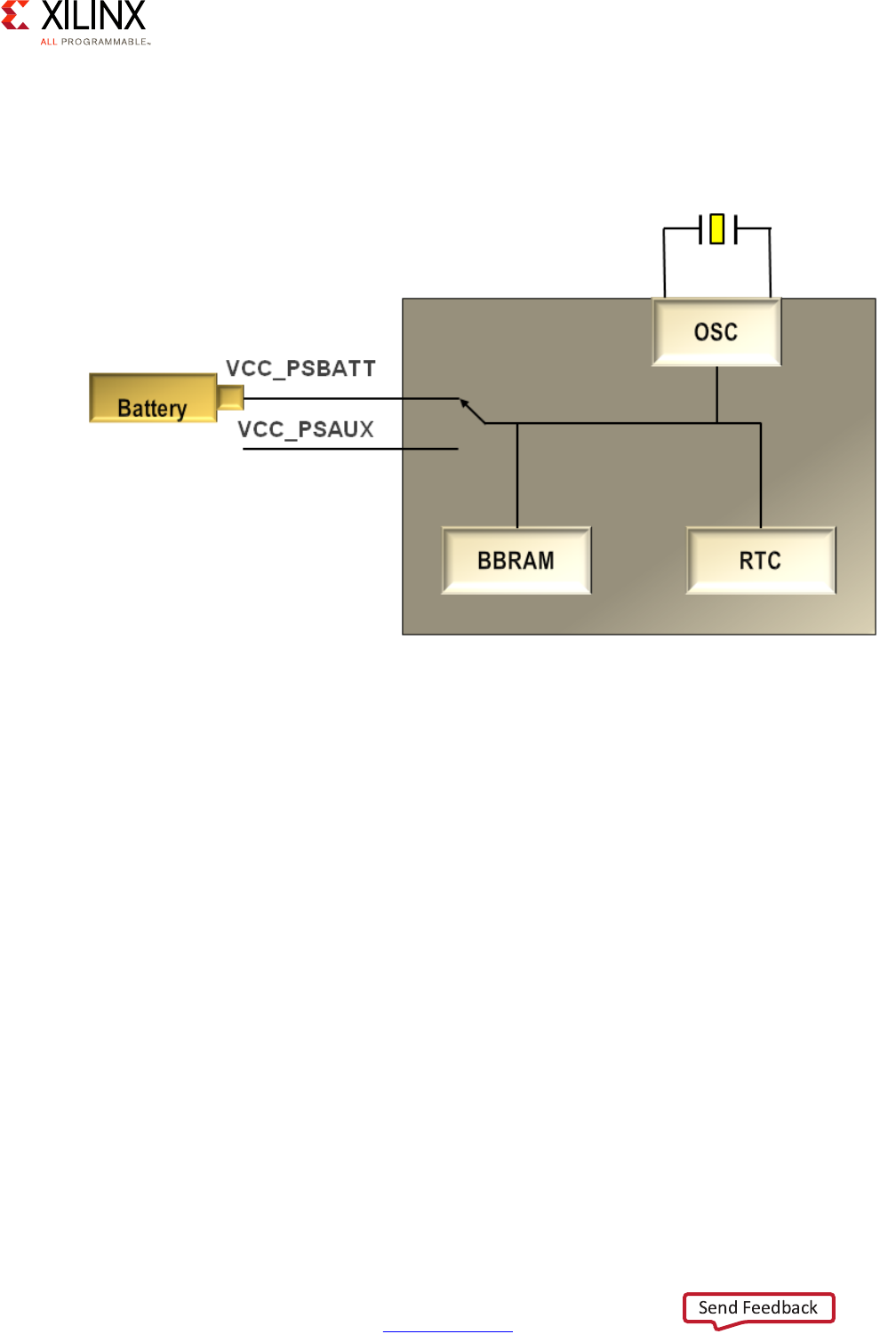
Zynq UltraScale+ MPSoC Embedded Design Methodology Guide 88
UG1228 (v1.0) March 31, 2017 www.xilinx.com
Chapter 4: Power Considerations
Battery Power Domain
The battery powered domain consists of the battery backed RAM for storing the encryption
key and real-time clock.
The battery backed RAM has the 256-bit device key optionally used for data decryption.
The real-time clock consists of a 40-bit timer and is a countdown-timer used when the rest
of the system is in sleep mode. It can be set (up to 40-bits) and will generate a periodic
interrupt to check the status of the system at a relatively low frequency (relative to the rest
of the clocks in the system). Typically a 32 kilohertz 'Watch' style crystal oscillator is hooked
up to it.
Typically the Zynq UltraScale+ device's battery power domain is always on, otherwise the
RTC would need to be reprogrammed the next time this power domain is enabled (i.e.
power is applied).
X-Ref Target - Figure 4-4
Figure 4-4: Battery Power Domain

Zynq UltraScale+ MPSoC Embedded Design Methodology Guide 89
UG1228 (v1.0) March 31, 2017 www.xilinx.com
Chapter 4: Power Considerations
Low Power Domain
The low power domain (LPD) consists of the real-time processor unit (RPU) with the R5
processors, the static on-chip memory (OCM), the platform management unit (PMU), the
configuration and security unit (CSU), and the low-speed peripherals:
X-Ref Target - Figure 4-5
Figure 4-5: Low Power Domain
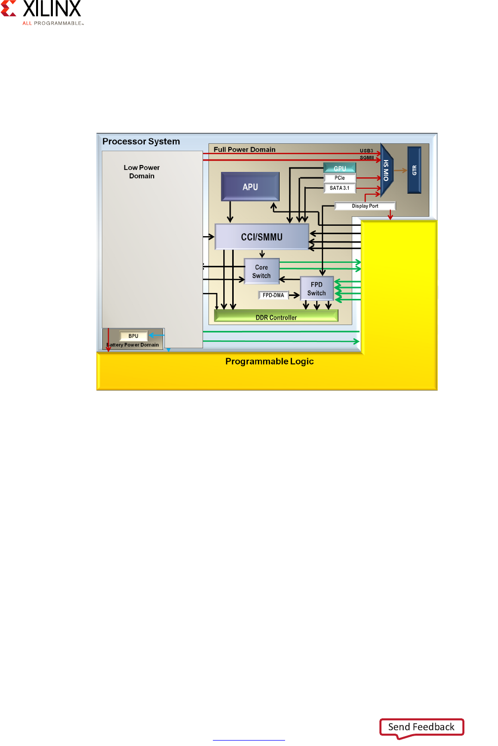
Zynq UltraScale+ MPSoC Embedded Design Methodology Guide 90
UG1228 (v1.0) March 31, 2017 www.xilinx.com
Chapter 4: Power Considerations
Full Power Domain
The full-power domain (FPD) consists of the APU with the A53 processors, the GPU, the
double data rate (DDR) memory controller and the high performance peripherals including
the PCI Express, USB 3.0, Display Port and SATA.
For clarity, note that this power domain cannot be enabled without the lower-power
domain being enabled, as the latter contains the PMU required for all power management
operations required for the former.
X-Ref Target - Figure 4-6
Figure 4-6: Full Power Domain
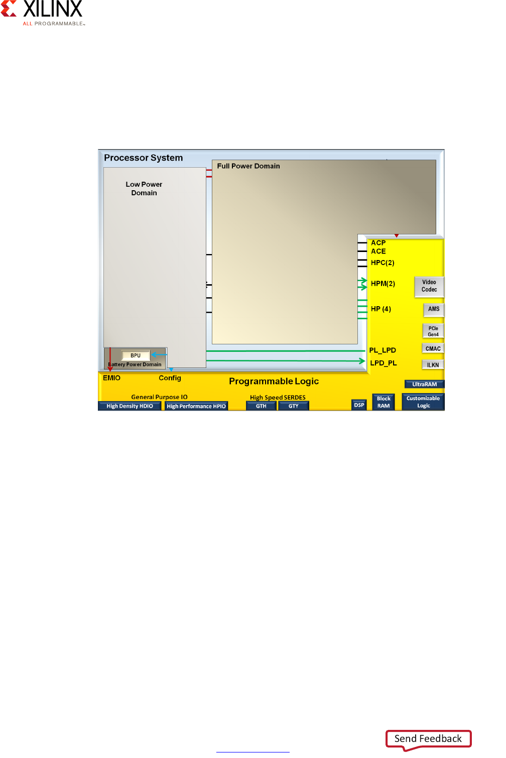
Zynq UltraScale+ MPSoC Embedded Design Methodology Guide 91
UG1228 (v1.0) March 31, 2017 www.xilinx.com
Chapter 4: Power Considerations
PL Power Domain
The Programmable Logic Power Domain consists of logic cells, block RAMs, digital signal
processing (DSP) blocks, AMS, Input/Output and high speed serial interfaces. Some
versions of the platform include the Video Codec, PCI Express Gen-4, UltraRAM, CMAC, and
Interlaken.
X-Ref Target - Figure 4-7
Figure 4-7: PL Power Domain

Zynq UltraScale+ MPSoC Embedded Design Methodology Guide 92
UG1228 (v1.0) March 31, 2017 www.xilinx.com
Chapter 4: Power Considerations
Power Islands and Power Gating
Within the low power and full power domains there are multiple power islands. This allows
for localized power gating within the device which does not require external power rails and
regulators.
Devices that can be gated include:
•Low Power Domain
°The R5s can be gated as a pair.
°The TCMs and OCM are broken into four banks each that can be individually gated
or held in retention mode.
°The USBs can each be individually gated.
• Full Power Domain
°Each of the A53s can be individually gated.
°L2 cache
°GPU - each pixel processors can be individually gated while the geometry processor
and L2 cache can be clock gated together.
Note that Power-Islands are initially powered up unless disabled by e-fuse. After power-on
via user code the PMU can quickly power-down appropriate islands.
Both in terms of feature disabling and in terms of dynamic power management, it is worth
spending some time considering the available power islands and when or whether they are
needed in your design. If, for instance, your system has neither a user interface nor USB
connectivity, you probably want to turn off the USB and GPU power islands at startup by
instructing the PMU to do so. You can also use clock gating to reduce the power usage of
some of the peripherals as needed.

Zynq UltraScale+ MPSoC Embedded Design Methodology Guide 93
UG1228 (v1.0) March 31, 2017 www.xilinx.com
Chapter 4: Power Considerations
Platform Management Unit
The Platform Management Unit (PMU) is responsible for two major functions:
• Power Management
• Safety Management
It includes a dedicated Boot ROM that handles power up, power down and reset requests.
The PMU also supports Inter-Processor Interrupts (IPI) for communication between the
system processors.
The PMU processor is connected to 128 kilobytes of RAM with error-correcting code (ECC)
that is used for data and firmware as well as storage of the Xilinx provided framework code.
The PMU provides global registers including power, isolation, reset, Logic Clear, Error
Capture and System Power State registers which will be used by the Xilinx® Power
Management Firmware.
The PMU includes its own local registers, as well as a dedicated Interrupt Controller.
Interfaces exist to and from the PMU, the Processing System I/O and the Programmable
Logic (PL).
The higher you feel your power requirements are, the more time you should spend studying
the PMU and its capabilities.
X-Ref Target - Figure 4-8
Figure 4-8: Platform Management Unit Block Diagram

Zynq UltraScale+ MPSoC Embedded Design Methodology Guide 94
UG1228 (v1.0) March 31, 2017 www.xilinx.com
Chapter 4: Power Considerations
Functions at Power On
After power on, the PMU performs the following sequence of events before handing off to
the Configuration Setup Unit (CSU):
• Provides power integrity check using the system monitor (SysMon) assuring proper
operation of the CSU and the rest of the LP domain.
• Initializes the PLLs
• Triggers and runs the Memory Built in Self Test (MBIST)
• Captures and signals errors which can be read through JTAG
• Powers down any Power Islands and other IP disabled via eFuse
• Releases Reset to CSU
Xilinx PMU Firmware
The PMU Firmware provided by Xilinx extends what's already in the ROM and provides
additional functionality for customers. The firmware is a framework provided for power and
safety management functions and is available as source code for easy customization and
extension.
The firmware uses IPI to communicate with other on-chip masters. It handles safety
features, including error handling and RAM scrubbing.
The PMU Boot ROM (PBR) offers two interrupt handling modes:
•Hook Mode
• Complete Replacement Mode
With the first mode PMU Interrupts can go directly to the ROM and then are handled by the
Interrupt Service Routines (ISR) within the ROM.
In the second mode, Complete Replacement Mode, the interrupt handler in the ROM is
replaced by code that is residing in the RAM. The PMU Firmware is implemented using that
latter mode.
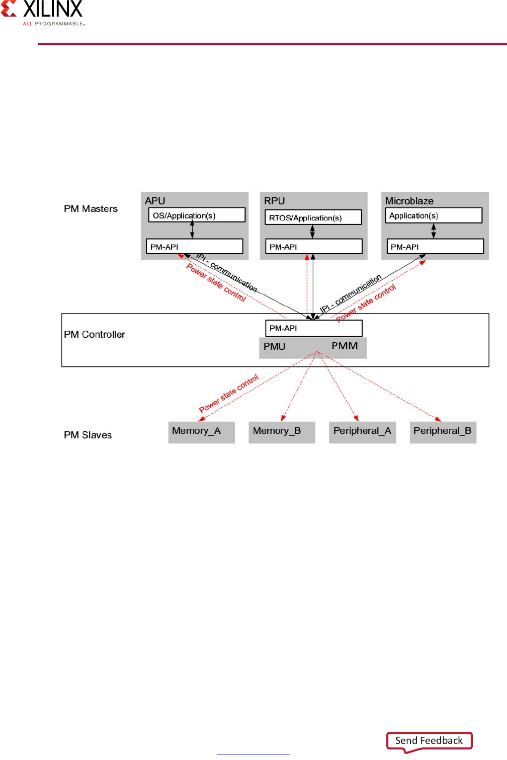
Zynq UltraScale+ MPSoC Embedded Design Methodology Guide 95
UG1228 (v1.0) March 31, 2017 www.xilinx.com
Chapter 4: Power Considerations
Power Management Software Architecture
To enable multiple processing units to cooperate in terms of power management, the
software framework for the Zynq UltraScale+ MPSoC device provides an implementation of
the power management API for managing heterogeneous multiprocessing systems. The
following figure illustrates the API-based power management software architecture.
The PMU Run-Time Software Functions include:
• Enabling system power-down modes
• Managing the system during the power-down modes and wakes up the system based
on various triggering mechanisms
• Maintaining the System Power State at all time
• Acting as a delegate to the Application and Real-time processors during their sleep
state and initiates their power up and restart after their wake-up request
Refer to the Embedded Energy Management Interface (EEMI) API User Guide (UG1200) [Ref 6]
for additional details regarding the use of the various APIs available for power
management.
X-Ref Target - Figure 4-9
Figure 4-9: Power Management Software Architecture
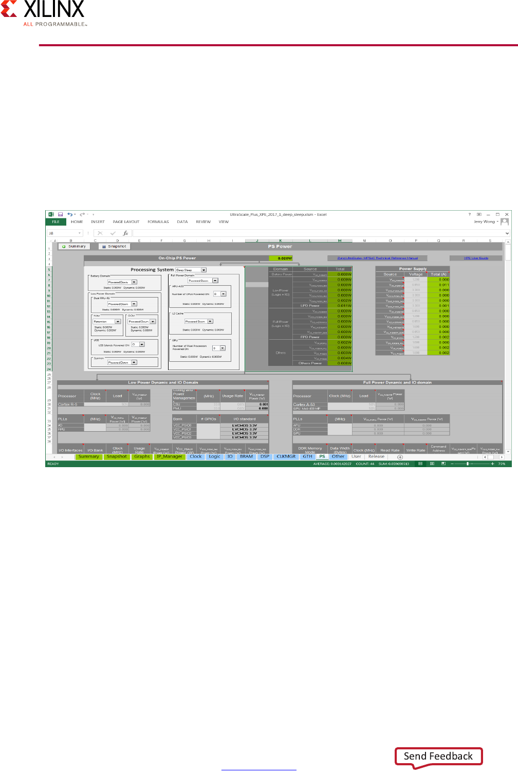
Zynq UltraScale+ MPSoC Embedded Design Methodology Guide 96
UG1228 (v1.0) March 31, 2017 www.xilinx.com
Chapter 4: Power Considerations
Xilinx Power Estimator
Xilinx provides a publicly available tool to rapidly estimate power consumption for a target
device. This tool provides the ability to select the device type, packaging, silicon
speedgrade, temperature grade and an optional estimate for typical or "maximum" silicon.
The tool provides the ability to select what processor cores are active, what their utilization
level is, what memory type is planned and its utilization, and what peripherals are in use.
Similarly, for the programmable logic selection of what IP blocks are used, their clock
frequencies and utilization can be made.
Refer to the Xilinx Power Estimator User Guide (UG440) [Ref 1] for more information.
X-Ref Target - Figure 4-10
Figure 4-10: Xilinx Power Estimator
Zynq UltraScale+ MPSoC Embedded Design Methodology Guide 97
UG1228 (v1.0) March 31, 2017 www.xilinx.com
Chapter 5
Programmable Logic
All Zynq® UltraScale+™ MPSoC devices integrate Programmable Logic, including several
interfaces that allow for communication between the Processing System (PS) and the
programmable logic (PL). The scope of this chapter is to focus on all considerations on
designing with the interfaces between PS and PL. Design considerations that govern
interaction between various features of the PL are is not in the scope of this chapter.
However, it is very important for the designer to understand thoroughly the various
features of the PL. These are covered comprehensively in UltraFast Design Methodology
Guide for the Vivado Design Suite (UG949) [Ref 4].
Defining Your PL Needs
Understanding your PL needs is a fundamental part of your system design. The size of the
PL and the features available vary depending on the device chosen. Hence, first, it is
important to understand the needs from a system perspective and select the right kind of
device. The various devices and their PL capabilities are shown in the device tables on the
Xilinx All Programmable Heterogeneous MPSoC web site [Ref 18]. Defining the needs
upfront also enables the system designer to make the right kind of choices on how to set up
communication between the PS and PL. .
This chapter assumes that you have knowledge in designing with programmable logic in
FPGAs. Specifically, it is assumed that you already know how to select a properly-sized part
to take into account the amount of logic required for any custom and off-the-shelf IP
needed by your design.
TRAINING: For further reference, Xilinx provides a comprehensive set of documentation, training and
tutorials to get started. Training information is available at https://www.xilinx.com/training.html.
You can start with the Hardware Developer Zone, located at
https://www.xilinx.com/products/design-tools/hardware-zone.html.
Zynq UltraScale+ MPSoC Embedded Design Methodology Guide 98
UG1228 (v1.0) March 31, 2017 www.xilinx.com
Chapter 5: Programmable Logic
The following questions will help in defining your needs with regards to PS-PL interaction:
• Do you need to transfer data between the PS and the PL?
• Do you have performance requirements (throughput and latency) on moving data to
and from memory attached to PS?
• Do you need to route interrupts between the PS and the PL?
• Is boot time and/or PL configuration critical?
• Does your IP in the PL need to be notified of resets?
• Do you need to receive clocks from the PS in the PL?
• Do you need to generate clocks in the PL to clock PS?
PL Methodology
As a reminder of the role of the PL in the overall system architecture, the following figure
illustrates the PL and its features, along with the communication interfaces between the PL
and the PS.
X-Ref Target - Figure 5-1
Figure 5-1: Zynq UltraScale+ MPSoC Programmable Logic
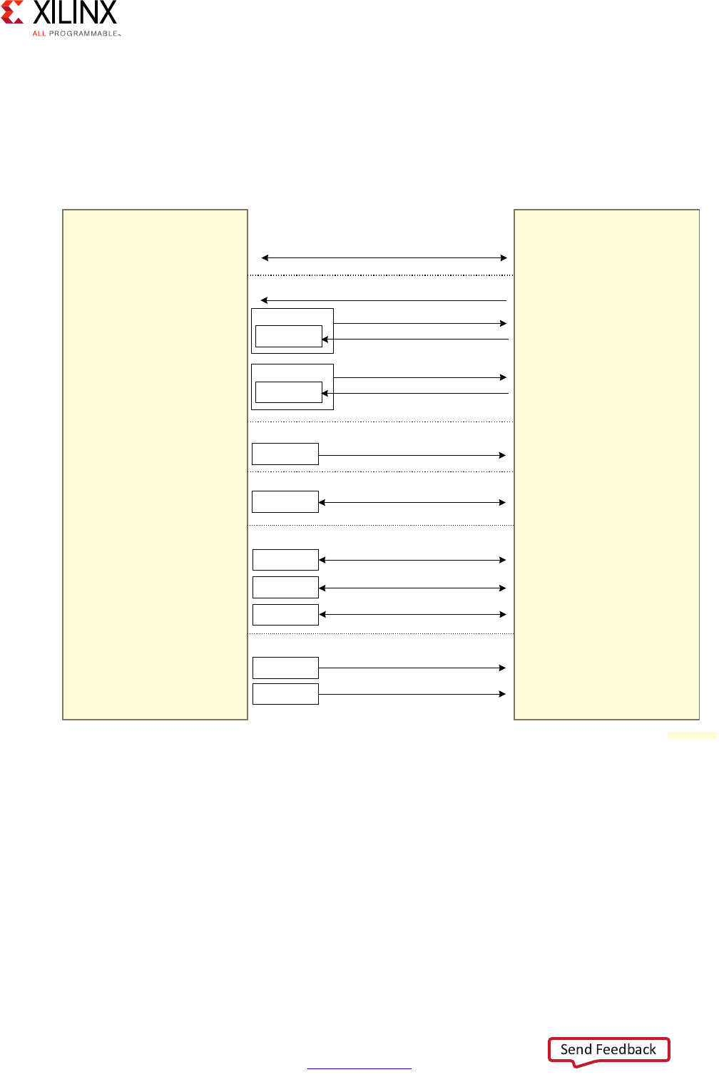
Zynq UltraScale+ MPSoC Embedded Design Methodology Guide 99
UG1228 (v1.0) March 31, 2017 www.xilinx.com
Chapter 5: Programmable Logic
As described above, the focus of the present PL methodology is on the interaction between
the PS and PL. To aid in illustrating it, a simplistic, yet accurate diagram is shown in
Figure 5-2.
Note: This diagram does NOT attempt to precisely represent the internal blocks of the Zynq
UltraScale+ device. Instead, it is primarily a conceptual view for the purposes of the present
explanation.
There are several types of connections to and from the PL area of the device as shown. Each
connection has important characteristics that could influence design. The connection types
are:
•AXI interfaces
•Interrupts
•Clocks
• EMIO, including resets (as GPIO through EMIO)
X-Ref Target - Figure 5-2
Figure 5-2: Zynq UltraScale+ MPSoC PS-PL Interface
Processing
System
Programmable
Logic
AXI Interfaces
There are several AXI Interfaces, see Fig 5-3 for details
Interrupts
FPD
APU
LPD
RPU
16 Shared Peripheral Interrupts
64 Peripheral Interrupts
4 IPI + 4 FIQ + 4 IRQ
100 Peripherals Interrupts
4 IPI + 2 nFIQ + 2 nIRQ
Clocks
LPD
4 Clocks
EMIO
96 EMIO bits (Use GPIO for Resets)
LPD
DisplayPort
Dedicated Stream
Dedicated Connections
PMU
Several Signals
GigEth
Dedicated Stream
DMA
FPD-DMA
Flow Control
LPD-DMA
Flow Control
(DMA transfers are done over AXI interfaces)
;
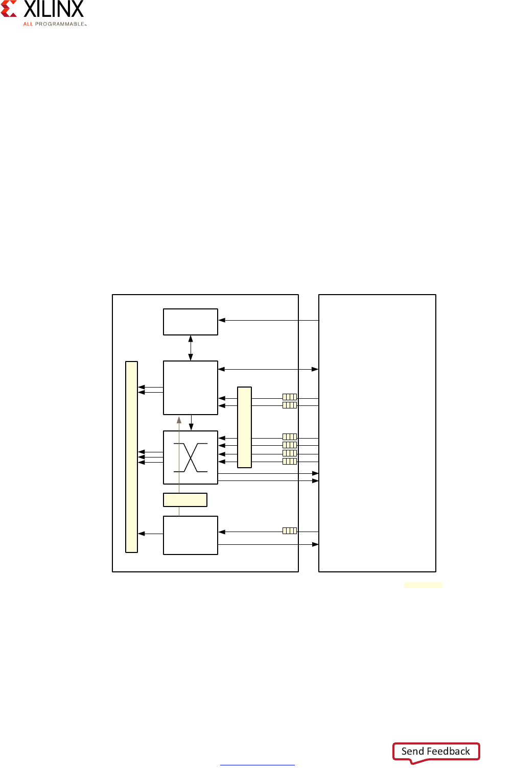
Zynq UltraScale+ MPSoC Embedded Design Methodology Guide 100
UG1228 (v1.0) March 31, 2017 www.xilinx.com
Chapter 5: Programmable Logic
• Dedicated streams
•PMU
•DMA
The following subsections describe each of these in detail.
AXI Interfaces
As covered in Chapter 2, Processing System, the core mechanism for cross-component
communication in the Zynq UltraScale+ MPSoC device is the ARM AXI interconnect. As
shown above, there are several AXI links between the PS and the PL. The choice of the AXI
link you use between the PS and PL is one of the most important choices to make when
designing your application around the Zynq UltraScale+ MPSoC device. For a better
understanding of the available choices, the following figure provides a detailed view of the
AXI interfaces shared between the PS and the PL.
X-Ref Target - Figure 5-3
Figure 5-3: Detailed PL/PS Communications AXI Interfaces
PS
S_AXI_ACP_FPD
APU
CCI
Memory Subsystem
LP
PL
S_AXI_ACE_FPD
S_AXI_HPC0_FPD
S_AXI_HPC1_FPD
S_AXI_HP0_FPD
S_AXI_HP1_FPD
S_AXI_HP2_FPD
S_AXI_HP3_FPD
SMMU
M_AXI_HPM0_FPD
M_AXI_HPM1_FPD
S_AXI_LPD
M_AXI_HPM0_LPD
SMMU
X15278-100116

Zynq UltraScale+ MPSoC Embedded Design Methodology Guide 101
UG1228 (v1.0) March 31, 2017 www.xilinx.com
Chapter 5: Programmable Logic
High Performance AXI Masters
The high-performance AXI4 ports provide access from the PL to the double data rate (DDR).
There are six such ports (2 S_AXI_HPCn_FPD and 4 S_AXI_HPn_FPD) outbound from the PL,
and they are configurable to 128, 64 or 32 bits. Two of those ports are connected the Cache
Coherent Interconnect (CCI), mentioned below, and four are connected directly to the DDR
interface for memory access.
Inbound AXI Slaves
A single, up to 128-bit wide, low-latency slave interface (M_AXI_HPM0_LPD) provides
communication between the PS and the PL from the LPD. Two inbound slave interfaces
(M_AXI_HPM0_FPD and M_AXI_HPM1_FPD) allow communication to the PL from the FPD.
Accelerator Coherency Port (ACP)
There is a 128-bit wide AXI slave interface (S_AXI_ACP_FPD) that provides connectivity
between the APU L2 cache controller and potential accelerator functions in the PL. This
slave interface shares a coherent view of the CPU L2 cache through a snooping process,
where the PL keep the CPU cache up to date. Given that coherency from the PL to the CPU
is not maintained by default, this interface is ideal for acceleration features in the PL that
rely on data already loading into the CPU cache.
AXI Coherency Extension
The AXI coherency extension (ACE) is a 128-bit AXI slave interface (S_AXI_ACE_FPD) that
provides connectivity between the APU and potential accelerator functions in the PL. Unlike
the ACP, this slave shares coherent access to the CCI. The ACE snoops access to the CCI and
the PL side, thus, providing two-way coherency in hardware. The PL includes one such
master interface to the PS.
For more information about PL/PS communication, see this link in the Zynq UltraScale+
MPSoC Technical Reference Manual (UG1085) [Ref 7].
For more information about software and hardware coherency, see this link in the Zynq
UltraScale+ MPSoC: Software Developers Guide (UG1137) [Ref 5].
Choosing Appropriate AXI Interfaces
The designer has to make some trade-offs on utilizing/assigning interfaces. Several choices
affect the decision. First, the direction of the pins (some are bi-directional, some are
uni-directional and can be from or to the PL). Some interfaces provide coherency, some
provide protection (being in low-power domain (LPD) for safety, and some provide
performance benefits (latency and throughput). The following table summarizes the
available AXI interfaces based on direction and required feature.
Zynq UltraScale+ MPSoC Embedded Design Methodology Guide 102
UG1228 (v1.0) March 31, 2017 www.xilinx.com
Chapter 5: Programmable Logic
If, for instance, you need an outbound link from the PL that will survive even if the FPD is
down, the S_AXI_LPD is likely a good choice. On the other hand, if you need a
fully-coherent bi-directional link between the PS and the PL then S_AXI_ACE_FPD is likely
a better choice.
It is imperative to take the appropriate time to weigh the pros and cons of using the
available links as the rest of your architecture is likely to grown based on that choice. In
short, it will likely become very expensive to change your mind later on.
Interrupts
Serving and receiving interrupts from the PL is likely another important part of your design.
While table 35-6 in the Zynq UltraScale+ MPSoC Technical Reference Manual (UG1085)
[Ref 7] provides a full list of interrupts coming into and leaving the PL, the methodology
diagram presented earlier provides a good summary of the available interrupts. Namely:
• Inbound interrupts to PL:
°100 LPD peripherals
°64 FPD peripherals
• Outbound interrupts from PL:
°16 shared peripheral interrupts to the PS
°4 Inter-Processor interrupts, 4 FIQs and 4 IRQs to the APU
°4 Inter-Processor interrupts, 2 nFIQs and 2 nIRQs to the RPU
You can use any of the inbound interrupts to trigger behavior in your PL IP, and you can
trigger interrupts in the PS by asserting any of the outbound interrupts available. Which
multimediayou choose will invariable be application-dependent.
Bi-Directional From PL To PL
Coherent S_AXI_ACE_FPD S_AXI_HPC0_FPD,
S_AXI_HPC1_FPD
N/A
Belongs to LPD N/A S_AXI_LPD M_AXI_HPM0_LPD
Performance N/A S_AXI_ACP_FPD N/A
General-purpose,
non-coherent
N/A S_AXI_HP0_FPD,
S_AXI_HP1_FPD,
S_AXI_HP3_FPD,
S_AXI_HP4_FPD,
M_AXI_HPM0_FPD,
M_AXI_HPM1_FPD

Zynq UltraScale+ MPSoC Embedded Design Methodology Guide 103
UG1228 (v1.0) March 31, 2017 www.xilinx.com
Chapter 5: Programmable Logic
Clocks
If you need to receive a clock signal from the PS, you can use any of the four clocks sent by
the boundary of the PL. Note that these clocks are operated independently and that there
is no guaranteed timing relationship between their signals. As such, your PL IP should not
depend on implicit synchronization between the clocks incoming from the PS.
EMIO
As described in Chapter 10, Peripherals, the EMIO mechanism is a way to map LPD
peripheral output pins to the PL. EMIO can also be used as a easy way to bi-directionally link
the LPD to the PL. It can, for instance, be used to generate resets from the PS for use by the
PL by mapping LPD GPIO output to PL functionality. Note that there are no dedicated resets
between the PS and the PL.
Dedicated Streams
Some functionality, such as the Gigabit Ethernet controllers in the LPD and DisplayPort in
the FPD, have dedicated streams connected to and from the PL. The Gigabit Ethernet
controller is discussed in the Peripherals Chapter. The DisplayPort is discussed in the
Multimedia Chapter. For specific details about how those peripherals interact with the PL,
refer for the Zynq UltraScale+ MPSoC Technical Reference Manual (UG1085) [Ref 7].
PMU
The PMU and the PL share several signals:
• 32 bits of General Purpose Input (GPI) and General Purpose Output (GPO)
• AIB request and ack signals for both LPD and FPD
• 4 error outputs from the PL provided as inputs to the PMU
• 47 outputs from the PS indicating error to the PL
These can be useful to you if you need your PL IP to tightly coordinate with the PMU for
mission-critical applications.
DMA
Both the FPD-DMA and the LPD-DMA can provide flow control signals in the PL. Refer to
Chapter 6, Memory for more information about the DMA controllers.
Zynq UltraScale+ MPSoC Embedded Design Methodology Guide 104
UG1228 (v1.0) March 31, 2017 www.xilinx.com
Chapter 5: Programmable Logic
Logic
This section refers to the features of PL which are made of look-up tables (LUTs) and Flip
Flops. Designers can implement custom RTL and use Xilinx® Tools to program them. In
order to connect them to the PS, the designer must implement AXI interfaces on all logic
that is required to communicate with the PS for data transfers. If there is more than one
interface that requires to communicate the PS, the designer should instantiate AXI
Interconnect IP to allow multiple masters to talk to multiple slaves. Inclusion of AXI
Interconnect will add to the amount of logic being used for connectivity. Planning ahead
will ensure optimal use of logic resources.
This section overviews the available tools, methodologies, and libraries that allow you to
design with the logic resources in the PL.
Note: For general information on Xilinx Tools that help you design all aspects of your device, see the
Developer Zone.
Vivado Design Suite
The Vivado® Design Suite integrated development environment (IDE) is industry's first
SOC-strength design suite suited for designing hardware solutions. It includes the
following:
•Vivado HLS: A High Level Synthesis compiler that converts C-based algorithms to
hardware IP.
•Vivado IP integrator: A block-based IP Integration tool that integrates IP from a large
Xilinx IP library.
•Vivado Logic Analyzer: A "Mixed Language Simulation Tool" that includes a logic
analyzer for system debugging on the target environment (Vivado Logic Analyzer).
•TCL: A tool command language that is the underlying scripting language used
throughout Vivado.
•Xilinx Software Development Kit (SDK): Another IDE for creating embedded
applications on any Xilinx microprocessors, including the MicroBlaze™ soft-core
microprocessor. You can use the Xilinx SDK to produce the applications run by your
FPGA. The Xilinx SDK can be optionally installed as part of your Vivado Design Suite
installation. For information about the Xilinx SDK, see the Xilinx Software Development
Kit web page [Ref 14].
Because Vivado is a complete IDE, it allows end-to-end development of all the logic you
need in your FPGA including support to create the encrypted bitstream used to configure
PL. Vivado provides acceleration for high level design, verification, and implementation.
Several Vivado editions exist (HL System, HL Design, and HL Webpack™). To find out more
about Vivado, see the Vivado Design Suite web page [Ref 15].

Zynq UltraScale+ MPSoC Embedded Design Methodology Guide 105
UG1228 (v1.0) March 31, 2017 www.xilinx.com
Chapter 5: Programmable Logic
Isolation Design Flow
The Xilinx Isolation Design Flow (IDF) was developed to allow independent functions to
operate in a partitioned manner on a single FPGA. Irrevocable physical separation of
functions and data, for example, is critical in a solution that uses the red/black concept,
which needs to be sure sensitive (red) and non-sensitive (black) data or functions never
infringe upon one another.
The IDF is a methodology based on existing implementation tool flows. Additional time
spent floorplanning the design is done using existing constraint tools (PlanAhead / Vivado
GUI). Verification of work products (pinout and routed design) are done with a separate and
independent tool (either IVT or VIV for the ISE® Design Suite or Vivado, respectively).
Using IDF, you can be sure that all the IP implemented in the programmable logic (PL) is
partitioned such that resource isolation and security needs are met. Xilinx provides several
reference designs that showcase IDF. You can get information on IDF at the Isolation Design
Flow web page [Ref 16].
Developing a safe and secure single chip solution containing multiple isolated functions in
a single FPGA is made possible through this Xilinx partition technology. Special attributes
such as SCC_ISOLATED and the features it enables are necessary to provide controls to
achieve the isolation needed to meet certifying agency requirements. To better understand
the details of the IDF, the designer should have a solid understanding of the standard
partition design flow. Many of the terms and processes in the partition flow are utilized in
the IDF. Areas that are different supersede the partition design flow and are identified in
Xilinx-supplied application notes:
Note: The Isolation Design Flow for Xilinx 7 Series FPGAs or Zynq-7000 AP SoCs (Vivado Tools)
application note presents the IDF using the Vivado Design Suite. Even though the application note is
for the Zynq 7000 AP SoCs, the concepts apply to the Zynq UltraScale+ MPSoCs.
In the IDF Methodology, the concept is to create isolated areas within the FPGA. The
following figure shows an example design.
Zynq UltraScale+ MPSoC Embedded Design Methodology Guide 106
UG1228 (v1.0) March 31, 2017 www.xilinx.com
Chapter 5: Programmable Logic
This example FPGA has an I/O Band, a Compare logical block, an advanced encryption
standard core (AES), and a redundant AES (AES_R). Each area is logically separate and
"partitioned" off from the other. Only controlled and trusted communication can occur
between each logical block.
You can achieve a secure or safety-critical solution while using FPGA design techniques and
coding styles with only moderate modifications to the traditional FPGA development flow.
IDF development requires you to consider floorplanning much earlier in the design process
to ensure that proper isolation is achieved in logic, routing, and I/O buffers (IOBs).
Additionally, the development flow is partition-based (i.e. each function a user desires to
isolate must be at its own level of hierarchy).
At this point, you can take one of two approaches:
• If you want to ensure unwanted optimization of redundancy does not occur, you must
synthesize each isolated function and implement them independently of the other
partitions. After you implement each partition, the design is merged into a flattened
FPGA design for device configuration.
• If you want to use other techniques to prevent such optimization, you can synthesize
the full design while being careful to maintain at least one level of hierarchy such that
IDF constraints can be applied to each partition that requires isolation.
While this flow requires you to break away from traditional FPGA development flows, the
partition approach does have certain advantages. If an isolated partition requires a change
late in the design cycle, only that specific function is modified while the remaining
partitions remain unchanged.
X-Ref Target - Figure 5-4
Figure 5-4: Isolation Design
COMPARE
AES
AES_R
I
N
O
U
T
led
push_
button
reset
data_pins
clk
key_pins
key_addr
key_sel
mode
I
N
O
U
T
X1086_01_113012
AES_R
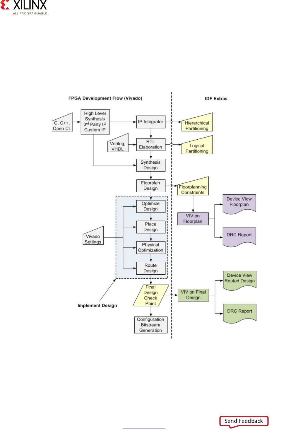
Zynq UltraScale+ MPSoC Embedded Design Methodology Guide 107
UG1228 (v1.0) March 31, 2017 www.xilinx.com
Chapter 5: Programmable Logic
Note: All logic should belong to an isolated partition except for global clocks, resets, and IOBs.
Figure 5-5 shows the typical FPGA design flow with the extra IDF steps considered to the
right. You must be sure to consider both hierarchical and logical partitioning. Both these
considerations ensure that your functions are separated and cannot corrupt one another.
You can use the IDF verification tools (VIV) to help with floorplanning constraints and
verification of the design.
X-Ref Target - Figure 5-5
Figure 5-5: Isolation Design Flow
Zynq UltraScale+ MPSoC Embedded Design Methodology Guide 108
UG1228 (v1.0) March 31, 2017 www.xilinx.com
Chapter 5: Programmable Logic
Xilinx Intellectual Property
Xilinx and its Partners have a rich library of Intellectual Property (IP), which is rigorously
tested, from which you can draw to develop your FPGA. The library consists of categories
that cover IP such as the following:
• Interface and Interconnect
• Communications
• IP Utility
•DSP and Math
•Memory and Controllers
• Device Family
•Embedded
• Audio and Video Imaging
• Market-Specific IP
You can browse the IP library at
https://www.xilinx.com/products/intellectual-property.html.
As mentioned in Vivado Design Suite, page 104, the Vivado IP integrator enables rapid
connection of IP that is enabled by a common user interface that is AXI-based. This tool can
reduce the design effort by months. Included in the IP Library are IP Subsystems that
integrate multiple IP into one solution.
Integrated IP Support
The PL includes integrated blocks for PCI Express, Interlaken, 100G Ethernet, System
Monitor, and the Video Codec Unit. The use of any of these will highly depend on your
application use case. The following subsections provide a brief introduction to these PL
peripherals.
For more information on the peripheral support for these devices, see this link in the Zynq
UltraScale+ MPSoC Technical Reference Manual (UG1085) [Ref 7].
PCI Express
The FPGA implements transaction layer, data link layer, and physical layer functions to
provide complete PCI Express endpoint and root-port functionality with minimal FPGA logic
utilization.

Zynq UltraScale+ MPSoC Embedded Design Methodology Guide 109
UG1228 (v1.0) March 31, 2017 www.xilinx.com
Chapter 5: Programmable Logic
These functions provide the basis to build a compatible Root Complex that allows custom
chip-to-chip communication using the PCI Express protocol and to also attach ASSP
Endpoint devices to the MPSoC (e.g. Ethernet controllers or Fibre Channel HBAs).
Depending on your system design requirements, you can configure this block to operate on
1, 2, 4, 8, or 16 lanes at up to 2.5 Gb/s, 5.0 Gb/s, 8.0 Gb/s, or 16 Gb/s data rates.
Interlaken
Interlaken IP is optimized for high-bandwidth and reliable packet transfers. The IP provides
chip-to-chip interconnect protocol that enables lane logic and protocol logic. The protocol
logic can be scaled up to 150 Gb/s. You can configure the logic up to 12 lanes using
12.5 Gb/s or 1 to 6 lanes up to 25.78125 Gb/s. With multiple Interlaken blocks, certain
UltraScale architecture-based devices enable easy, reliable Interlaken switches and bridges.
100G Ethernet
IEEE Std 802.3ba-compliant Ethernet integrated blocks provide low latency 100 Gb/s
Ethernet ports with a wide range of user customized solutions and statistics gathering. Zynq
UltraScale+ MPSoC 100G Ethernet blocks contain a Reed-Solomon forward error correction
(RS-FEC) block, which is compliant to IEEE Std 802.3bj, that you can use with the Ethernet
block or in stand-alone user applications.
System Monitor
As described in Chapter 8, Security, the system monitor block is used to enhance the overall
safety, security, and reliability of the system by monitoring the physical environment using
on-chip power supply and temperature sensors. You can use the System Monitor to monitor
voltage, measure current, measure sensor output, and in an external multiplexer mode used
when there is a shortage of IO ports connecting required external analog signals.
The System Monitor in the PL uses a 10-bit, 1 mega-sample-per-second (MSPS) ADC to
digitize the sensor outputs. The measurements are stored in registers and are accessed
using the advanced peripheral bus (APB) interface by the processes and the PMU in the PS.
Note that the System Monitor in the PL can be used as a general-purpose A/D converter.
Video Codec Unit
The Zynq® UltraScale+™ MPSoC video codec unit (VCU) available in the “EV” series
provides multi-standard video encoding and decoding, including support for the
high-efficiency video coding (HEVC) H.265 and advanced video coding (AVC) H.264
standards. The VCU is an integrated block in the PL of selected Zynq UltraScale+ MPSoCs
with no direct connections to the PS. The VCU operation is register programmable.
For more information on the VCU, see the "VCU" section in Chapter 9, Multimedia.
Zynq UltraScale+ MPSoC Embedded Design Methodology Guide 110
UG1228 (v1.0) March 31, 2017 www.xilinx.com
Chapter 5: Programmable Logic
Configuration and Partial Reconfiguration
As is explained in Chapter 3, System Software Considerations and Chapter 8, Security, the
PL is configured by the FSBL at startup by way of using the PCAP of the CSU. Sometimes it
might be desirable to have the PL only partially loaded by the FSBL during boot. It then
becomes necessary to proceed to partially reconfigure the PL later during the lifetime of
the system.
In essence, partial reconfiguration is the ability to dynamically modify blocks of logic by
downloading partial bitstreams while the remaining logic continues to operate without
interruption. To accomplish this, you must implement multiple configurations that
ultimately result in full bitstreams for each configuration, and partial bitstreams for each
module involved in partial reconfiguration. The number of configurations required varies by
the number of modules that need to be implemented.
For more information about partial reconfiguration, see the following:
•The Vivado Design Suite Tutorial: Partial Reconfiguration (UG947) [Ref 3]
• The Partial Reconfiguration web page [Ref 17]
• All configurations use the same top-level, or static, placement and routing results.
These static results are exported from the initial configuration, and imported by all
subsequent configurations using checkpoints.
FPGA technology provides the flexibility of on-site programming and re-programming
without going through re-fabrication with a modified design. Partial Reconfiguration takes
this flexibility one step further, allowing the modification of an operating FPGA design by
loading a partial configuration file, usually a partial .bit file. After a full .bit file configures
the FPGA, partial .bit files can be downloaded to modify reconfigurable regions in the FPGA
without compromising the integrity of the applications running on those parts of the device
that are not being reconfigured.
X-Ref Target - Figure 5-6
Figure 5-6: Partial Reconfiguration
FPGA
Reconfig
Block “A”
A4.bit
A3.bit
A2.bit
A1.bit
X12001
Zynq UltraScale+ MPSoC Embedded Design Methodology Guide 111
UG1228 (v1.0) March 31, 2017 www.xilinx.com
Chapter 5: Programmable Logic
The concept behind partial reconfiguration is to create all the bitstreams (full or partial) for
everything you want to be able to load up in the field. Ideally, you should know what
devices you will want to configure while the Zynq UltraScale+ MPSoC is running in the field.
Power Reduction Features
Power savings resulting from smaller 20 nm and 16 nm technology exist in the
Programmable Logic (PL). While optimal voltage tuning is the key enabler in
performance/watt ratios, Xilinx has also made numerous enhancements to architectural
blocks that were first delivered at 20 nm. Xilinx also introduced several brand new
technologies at 16 nm, such as UltraRAM, new PCI Express Gen4, and new types of I/O
banks.
Total power for each unique design is composed of four sources, which include Static,
Dynamic, Transceiver, and I/O power. The mix and match of these contributions depends on
the resources actually utilized, frequency, temperature and load. In comparing the Xilinx
28nm products and the UltraScale+ Architecture based FPGAs, power is lowered for all
power sources. Consequently, you can either lower your FPGA power budget by up to 50%
or with the same power budget, you now can deliver higher system performance based on
the same FPGA power budget.
These strides have been attained through several innovations in the UltraScale+
Architecture based FPGAs. For example, Xilinx has re-architected the transceivers to lower
power by 50% as compared to its previous generation. Multi-mode IO mode is still available
in the UltraScale+ Architecture based FPGA to offer significant power saving in
high-performance memory and LVDS interfaces. Features such as fine grained clock gating
works seamlessly with the Vivado IDE to provide significant dynamic power reduction in
logic. Block RAM also has many power saving features. The following figure summarizes
the built-in power optimizations of the Zynq UltraScale+ MPSoC device.
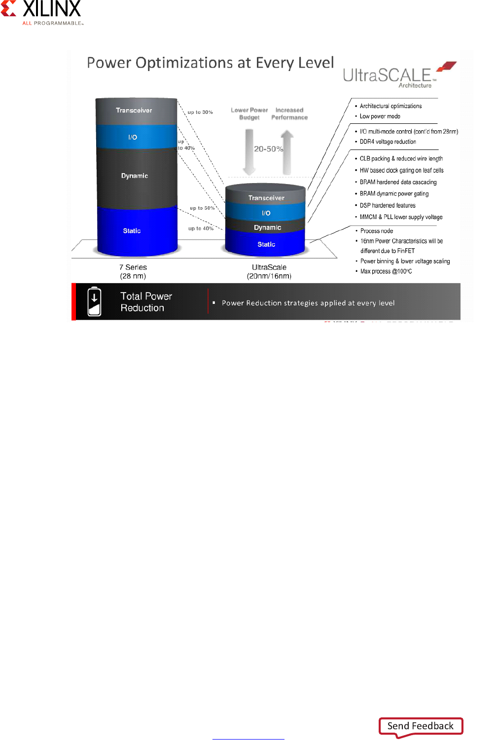
Zynq UltraScale+ MPSoC Embedded Design Methodology Guide 113
UG1228 (v1.0) March 31, 2017 www.xilinx.com
Chapter 6
Memory
Memory Introduction
More so than with typical general-purpose computing processors, the unique
heterogeneous computing capabilities of the Zynq® UltraScale+™ MPSoC device make
proper memory configuration and use essential to its operation. The Zynq UltraScale+
MPSoC device includes several on-chip memory components, a number of control
mechanisms for memory accesses, and fast and efficient external memory interfaces. This
chapter covers the memory-related aspects of the Zynq UltraScale+ MPSoC device and the
recommendations for their use.
Defining Your Memory Needs
Identifying the memory needs of your application and how they relate to the Zynq
UltraScale+ MPSoC device is an important part of your design. As this chapter describes,
there are quite a few ways to configure and use memory on the Zynq UltraScale+ MPSoC
device. To best help guide your design with regards to memory needs around the Zynq
UltraScale+ MPSoC device, it is assumed that you’ve at least gone through the Processing
System methodology covered in Chapter 2, Processing System. More specifically, you
should have a general idea of how keys parts of your design are subdivided among the main
processing blocks of the Zynq UltraScale+ MPSoC device as covered in Chapter 2.
With that in mind, the following questions will help you prepare for customizing the
memory capabilities of the Zynq UltraScale+ MPSoC device to your needs:
• How much memory does each of your designs parts need at any point in time?
• What are those parts’ dynamic memory bandwidth needs, compared to one another?
• Do you need to partition your processing to securely isolate processing blocks?
• Does any of the data you manage need to be securely stored at all times?
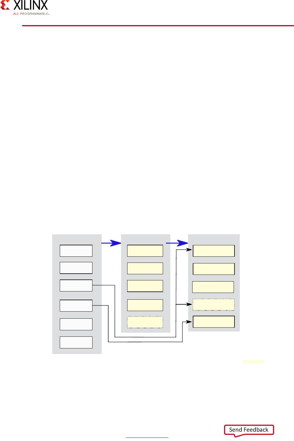
Zynq UltraScale+ MPSoC Embedded Design Methodology Guide 114
UG1228 (v1.0) March 31, 2017 www.xilinx.com
Chapter 6: Memory
Memory Methodology
There are several types of memory blocks in the Zynq UltraScale+ MPSoC device and
various paths between the Zynq UltraScale+ MPSoC device’s processing blocks and
memory. The architecture diagram presented in Chapter 1, Introduction provides the full
view of the system along with the memory components involved. For the purposes of the
present discussion, we’re going to use a simplified conceptual view of the Zynq UltraScale+
MPSoC device to better highlight the main parts related to memory and their relationships.
Note: This illustration does NOT attempt to precisely represent the Zynq UltraScale+ MPSoC
device’s internals. Instead, it’s primarily a conceptual view for the purposes of the present
explanation.
Specifically, we’re going to classify components participating in memory interaction as
falling in one of three broad categories:
• Users: Blocks that in one way or another access memory, no matter where it’s located.
• Arbitrators: Blocks which filter or condition memory accesses as they pass through.
• Providers: Blocks that provide actual memory storage.
The following diagram illustrates the relevant Zynq UltraScale+ MPSoC device blocks as
being part of one of those categories with the blue arrows illustrating the typical flow
followed by memory references:
Note: Note that this illustration does NOT attempt to precisely represent the Zynq UltraScale+
MPSoC device’s internals. Instead, it’s primarily a conceptual view for the purposes of the present
explanation.
X-Ref Target - Figure 6-1
Figure 6-1: Categories of Memory-Relevant Zynq UltraScale+ MPSoC Device Blocks
APU
GPU
RPU
Peripherals
DMA
PL
XMPU
Switch QoS
CCI
DDRC
ExternalMemory
OCM
PL
TCM
Users Arbitrators Providers
PL
Peripherals
X18700-032917

Zynq UltraScale+ MPSoC Embedded Design Methodology Guide 115
UG1228 (v1.0) March 31, 2017 www.xilinx.com
Chapter 6: Memory
In short, a user must generally go through one or, more likely, many Arbitrators before
actually reaching memory Providers. There are some exceptions. The RPU includes
Tightly-Coupled Memory (TCM) which is directly accessible to the R5s in the RPU through
a low-latency link. Also, the processing logic (PL) can be programmed to arbitrate access to
external memory and also provide memory usable either internally from other parts of the
PL or, less frequently, by the rest of the system.
Memory operations and accesses are heavily conditioned by the Zynq UltraScale+ MPSoC
device’s Interconnect, as described in Chapter 2, Processing System. Refer to that chapter
for more information regarding the role of Switch Quality of Service (QoS), Cache Coherent
Interconnect (CCI), and how to tweak the interconnects QoS to your needs if required. The
Xilinx memory protection unit (XMPU) is effectively a security block for filtering memory
accesses and is described in greater detail in Chapter 7, Resource Isolation and Partitioning.
For most applications, the on-chip memory (OCM), which is 256KB is size, and the R5s’ twin
TCMs, which are 128KB in size for each R5, are likely to be insufficient to build a
fully-functional system. Instead, external memory is likely always going to be part of your
design. Deciding on the size of the external memory to use for your design is therefore one
of the key decisions your team will need to make. Additionally, another key question that
you will need to answer is whether or not you need more bandwidth than offered by the
default DDR controller (DDRC). The vast majority of applications will be well-served by the
DDRC’s maximum bandwidth of 19,200MB/s. It is useful to understand how your application
uses this bandwidth and your options in case you need more.
As a rule of thumb, if your application requires around 60% or less of the DDRC’s maximum
bandwidth then the Zynq UltraScale+ MPSoC device will work for you as-is with regards to
memory. If your bandwidth is anywhere between 60 and 80% of that bandwidth, then you
should probably use the System Performance Monitoring (SPM) tool available in the Xilinx®
Software Development Kit (SDK) to model your memory usage on the Zynq UltraScale+
MPSoC device to get a better idea of how the system behaves under your workloads. The
SDK was mentioned in Customizing QoS, page 36 and is further discussed in Chapter 3,
System Software Considerations. As you approach 90% bandwidth, however, you are likelier
to need an additional external memory controller. Such a controller can be implemented in
the PL, thereby making the PL an Arbitrator of memory accesses as illustrated in the
previous diagram. While most applications will not require such a configuration, the need
for an additional memory controller is more likely to occur in systems involving video
processing or UltraHD.
External memory needs are also driven by size and ECC considerations.
Zynq UltraScale+ MPSoC Embedded Design Methodology Guide 116
UG1228 (v1.0) March 31, 2017 www.xilinx.com
Chapter 6: Memory
Built-In Memory Blocks
The Zynq UltraScale+ MPSoC device includes several built-in memory and memory-capable
blocks for use in different scenarios. This section will cover those blocks and their typical
uses.
On-Chip Memory
The On-Chip Memory (OCM) in the Processing System (PS) is 256 KB in size. OCM cannot be
accessed through the DDR controller. There are interfaces to the OCM from the PL and the
PS. The latter can access the OCM both from the Full-Power Domain (FPD) and the
low-power domain (LPD).
One reason to use the OCM memory over the DDR is to achieve greater performance since
the OCM’s latency is several cycles less than what the DDR controller can deliver, and it has
a higher bandwidth than the DDR. Strategic use of the OCM can therefore be useful in
circumstances where memory access speeds are essential, limited in size as it may be. One
way to optimize your use of the OCM for performance is to use strictly for storing data, not
code. You can then run the code from external memory or, in the unlikely case where you
aren’t using external memory or would prefer using external memory for other uses, you
can also use eXecute-In-Place (XIP) strategies to have the code run straight from, say,
Quad-SPI (QSPI)-based storage.
Another reason to use OCM instead of external memory is security. Since the OCM is
built-into the Zynq UltraScale+ MPSoC device, there’s no way for an attacker to readily
snoop data in transit between the various processing blocks and the OCM. Hence, the OCM
is a perfect location for securely-storing important transient data such as cryptographic
keys and sensitive information. If the objects to be stored are too large for the OCM, they
can be encrypted using temporary keys stored in the OCM and the encrypted objects sent
to external memory for storage. In that case the encrypted objects stored in the external
memory remain secured since the keys necessary to access them are confined to the OCM.
In general, software running on the application processing unit (APU) and real-time
processor unit (RPU) can access the OCM for their own use. In addition, there are other
specific scenarios where OCM is used. The First-Stage Boot Loader (FSBL), for instance,
loads the code for booting the PS into the OCM during boot process configuration stage,
whether the system is booted in secure more or not. The OCM is also used to program the
non-volatile flash memory through JTAG. In JTAG boot mode the routines responsible of
programming the flash memory are loaded in the OCM and take over the flashing process.

Zynq UltraScale+ MPSoC Embedded Design Methodology Guide 117
UG1228 (v1.0) March 31, 2017 www.xilinx.com
Chapter 6: Memory
Programmable Logic Memory
The PL can be configured to provide three different types of memory blocks. While the
amount of memory available inside the PL is limited, that memory requires less power and
is faster to access than external memory. It is also crucial for hardware design in the PL.
Hence, the configuration of some of the PL’s memory capabilities for general purpose use
by the Zynq UltraScale+ MPSoC device’s processing blocks should be a last resort.
The three types of memory in the PL have different characteristics and they can all be
instantiated within an FPGA design using the Xilinx development tools.
BRAM
Block RAM (BRAM) memory is a type of memory that has been available on previous Xilinx
FPGA processors. BRAM makes a small amount of memory usable by PL components. It
comes in 36 KB blocks and Zynq UltraScale+ MPSoC device devices can include up to 35 MB
worth of BRAM across the PL depending on the device type. BRAM units can be used as two
independent 18 Kb blocks or a single 36 Kb block. It can be configured to use two ports or
a single port. Multiple BRAM blocks can also be chained together to be used as a single
unit.
UltraRAM
UltraRAM is an FPGA RAM for Zynq UltraScale+ MPSoC device devices. Each UltraRAM
block is 288KB and there’s a maximum of 128 MB of UltraRAM available on the Zynq
UltraScale+ MPSoC device. UltraRAM is more dense than BRAM and using it requires less
space in the FPGA fabric. Increased density in the case of UltraRAM also leads to lower
power usage over BRAM.
LUTRAM
LUTRAM, or Distributed RAM, is present in limited quantity on the Zynq® UltraScale+™
MPSoC. Distributed RAM are memory blocks built out of LUT primitives in the PL.
Distributed RAM can be used by the PL designers when the need for memory is lower or if
the BRAM’s latency is not desired.
Tightly-Coupled Memory
Tightly-Coupled Memory (TCM) is 4 banks of 64 KB of memory attached to the real-time
processor (RPU) Cortex R5 processor cores. The TCM allows the RPU to have priority access
to memory that has deterministic performance and low-latency access.
As explained in Chapter 2, Processing System, the R5 processors can be set to function in
either Split or Lock-Step mode. The default mode of operation is Split mode. In this mode,
each Cortex-R5 processor contains two 64-bit wide 64 KB memory banks respectively called
ATCM and BTCM ports, for a total of 128 KB of memory. The division of the TCM into two
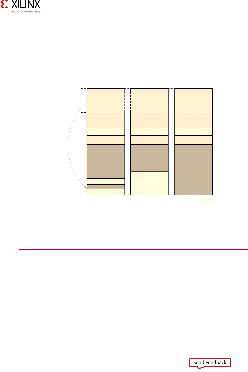
Zynq UltraScale+ MPSoC Embedded Design Methodology Guide 118
UG1228 (v1.0) March 31, 2017 www.xilinx.com
Chapter 6: Memory
parts allows the memory banks to be concurrently accessed by the R5 CPUs or by the AXI
interface. In Lock-Step mode, the TCMs can be combined into a single 256KB area. To allow
communication between the RPU and the rest of the PS, the TCM memory is also mapped
into the global system address map that is accessible by an APU or any other AXI master
that can access that map. The figure below illustrates the different ways in which the TCM
memory can be accessed.
Note: The global system address map is discussed in Global System Memory Map, page 119.
While the TCM is mapped inside the APU address space, the RPU always goes through a
direct low-latency path to access the TCM and does not go through any of the memory
arbitrators outlined earlier in this chapter.
PS DDR Memory and Controller
The Zynq® UltraScale+™ MPSoC PS DDR subsystem is connected to the rest of the system
through the Interconnect described in Chapter 2, Processing System using six AXI
interfaces. The DDR subsystem supports multiple memory standards (DDR3, DDR3L,
LPDDR3, DDR4, LPDDR4) and both UDIMMs and RDIMMs. The total DRAM capacity
supported is 32GB.
X-Ref Target - Figure 6-2
Figure 6-2: TCM Address Space as Seen by RPU and APU
Global Address Map
TCMs (256 KB)
LLPP + RPU-GIC
DRAM
BTCM (64 KB)
ATCM (64 KB)
0xFFFF-FFFF RPU Split View
Global Address Map
TCMs (256 KB)
LLPP + RPU-GIC
DRAM
BTCM (128 KB)
ATCM (128 KB)
RPU Lock-step View
Global Address Map
TCMs (256 KB)
APU-GIC
DRAM
APU View
GIC BaseAddr
Top of DRAM
TCMs alias
0x0000-0000
0xFFE0-0000
X15298-092916
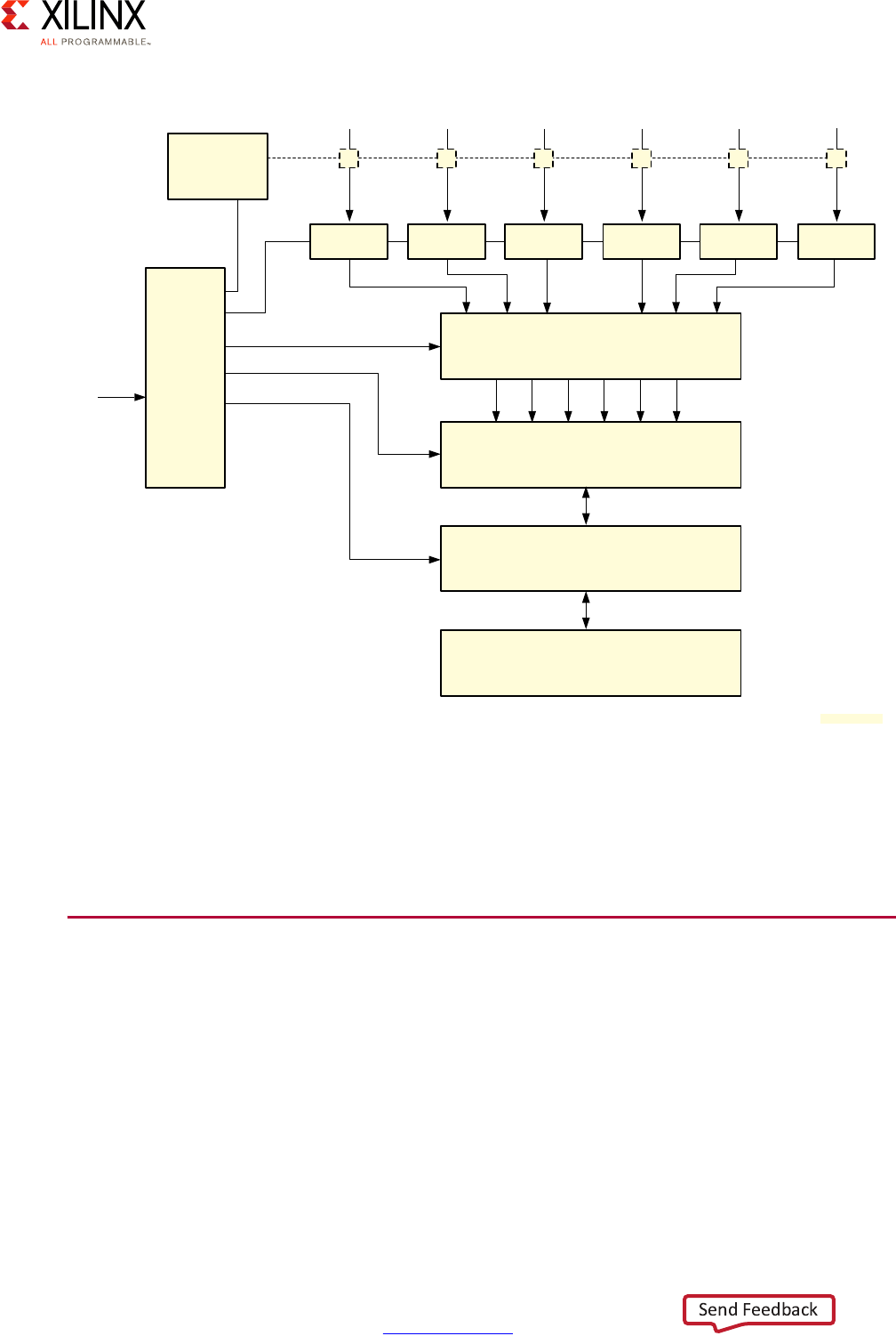
Zynq UltraScale+ MPSoC Embedded Design Methodology Guide 119
UG1228 (v1.0) March 31, 2017 www.xilinx.com
Chapter 6: Memory
Refer to Chapter 2, Processing System for more information on how the interconnect
operates and how to customize QoS. The “QoS Controller” illustrated above implements the
policies configured using the switch-based QoS and the CCI-based QoS described in the
corresponding sections of the that chapter.
Global System Memory Map
The Zynq UltraScale+ MPSoC device’s global system address map space spans 1TB and is
tailored to serve several types of AXI masters. The RPU’s R5s for instances are 32-bit
processors whereas the APU’s A53s are 64-bit or 32-bit processors. At a basic level, the A53s
in 64-bit mode can therefore address a lot more memory than the R5s. The 32-bit
processors can address up to 4GB whereas 64-bit processors can theoretically go up to
16EB; in practice though ARMv8-A only supports up to 48 bits of addressing. The system
memory map accommodates both types of AXI masters and is configurable to support 32,
36, or 40 bit system addresses.
X-Ref Target - Figure 6-3
Figure 6-3: DDR Subsystem Block Diagram
AXI
Performance
Monitor
XMPU0
From
RPU
XMPU1
From
CCI-400
XMPU2
From
CCI-400
XMPU3 XMPU4
From
AFI3/AFI4
2x2 Switch
XMPU5
From AFI5
FPD-DMA
2x2 Switch
QoS Controller
AXI to
APB
Bridge
DDR Memory Controller
DDR multiPHY
DDR3, LPDDR3, DDR4, LPDDR4
Standard DDR Memory Interface
From Top
Switch
From
AFI2/Display Port
2x2 Switch
X15348-092816
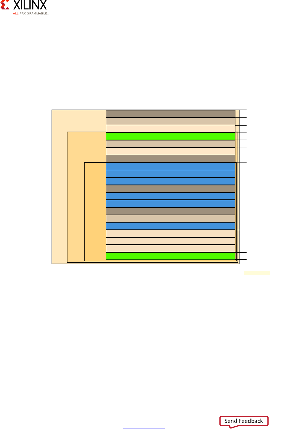
Zynq UltraScale+ MPSoC Embedded Design Methodology Guide 120
UG1228 (v1.0) March 31, 2017 www.xilinx.com
Chapter 6: Memory
Page table translation requires the memory management hardware to walk through page
tables to translate addresses between translation stages. The wider the address space, the
more tables to walk. With 4KB pages, for example, a 40-bit wide address requires walking
through 4 tables, a 36-bit address requires 3, and a 32-bit address requires 2. Hence, even
on processors capable of dealing with wider address spaces, there’s a benefit in using fewer
address bits in order to speed up memory accesses.
The Zynq UltraScale+ MPSoC device’s system address as shown below supports 32-bit
masters as well as optimized 36-bit access for 64-bit capable masters.
Note: That is 16 ExaBytes, or 16*1,024 PetaBytes, or 16*1,024*1,1024 TeraBytes.
By mapping essential system components, including the DDR, to the lower 32-bit
addressable space accessible to 32-bit capable masters, the Zynq UltraScale+ MPSoC
device ensures that those masters can use the majority of the on-chip peripherals and
capabilities. The 36-bit address space beyond that provides 64-bit masters with quick
access to the resources they are likely to most frequently need, including additional DDR.
Finally, the 40-bit address space ensures that 64-bit masters have extended access to the
Zynq UltraScale+ MPSoC device’s capabilities. 64-bit masters include APU, PCIe, SATA,
DisplayPort, full-power domain direct memory access (FPD-DMA), USB, gigabit Ethernet
MAC (GEM), SD, NAND, QSPI, configuration security unit (CSU) DMA, and low-power
domain direct memory access (LPD-DMA) interconnects.
X-Ref Target - Figure 6-4
Figure 6-4: Zynq UltraScale+ MPSoC Device System Address Map
FooDDR - 2GB
FooLPD-PL - 512 MB
FooHPM0 - 256MB
FooHPM1 - 256MB
QSPI - 512MB
FooLower PCIe - 256MB
FooReserved - 128MB
CoreSight STM 4MB per master ID - 16MB
RPU Low Latency Peripheral Port - 1MB
Reserved - 63MB
FPS Slaves Includes FPS Top Slaves - 16MB
LPS Slaves Includes LPS Top Slaves - 28MB
CSU/PMU/TCM/OCM - 4MB
Reserved - 12GB
FooPL - 8GB
FooPCIe - 8 GB
DDR - 32GB
PL - 448GB
PCIe - 256 GB
Foo
Reserved - 256GB
32-bit
Address
Space
36-bit
Address
Space
40-bit
Address
Space
0GB
2GB
3GB
4GB
16GB
24GB
32GB
64GB
512GB
768GB
1TB
X18701-032117

Zynq UltraScale+ MPSoC Embedded Design Methodology Guide 121
UG1228 (v1.0) March 31, 2017 www.xilinx.com
Chapter 6: Memory
PS DMA Controllers
As with most modern-day SoCs, the most efficient way for transferring large amounts of
data across the Zynq UltraScale+ MPSoC device is to use DMA controllers, thereby avoiding
active involvement on the part of the various CPU cores. The Zynq UltraScale+ MPSoC
device includes two general purpose DMA controllers and several peripheral-specific DMA
engines. The former support memory-to-memory, memory-to-I/O, I/O-to-memory and
I/O-to-I/O transfers. The latter is discussed in more detail in Chapter 10, Peripherals. Xilinx
also offers several PL DMA cores in the IP catalog.
One general-purpose controller is located in the full-power domain (the FPD-DMA) and the
other is located in the low-power domain (LPD-DMA). Both general-purpose DMA
controllers are identical and manage 8 independent DMA channels sharing a common
buffer internally for maximum AXI bandwidth use. They both support QoS, TrustZone,
OverFetch and unaligned transfers. Both can also fire interrupts for notifications, and
support two transfer modes: simple DMA and scatter-gather DMA.
One difference between the controllers is the size of their common buffer. The FPD-DMA is
connected to a 128 bit AXI bus and uses a 4K internal common buffer and the LPD-DMA is
connected to a 64 bit AXI bus and uses a 2K common buffer. The common buffer is
managed automatically by the controller but the programmer can have some leverage on
each channel buffer usage by tweaking each channel’s rate-controller and read-issuing
registers.
The other difference between the controllers is that the LPD-DMA is I/O coherent while the
FPD-DMA isn’t. The LPD-DMA transfers are I/O coherent because they go through the CCI
while the FPD-DMA ones go directly to the DDR without going through the CCI. FPD-DMA
transfers therefore need software support in order to ensure coherency.
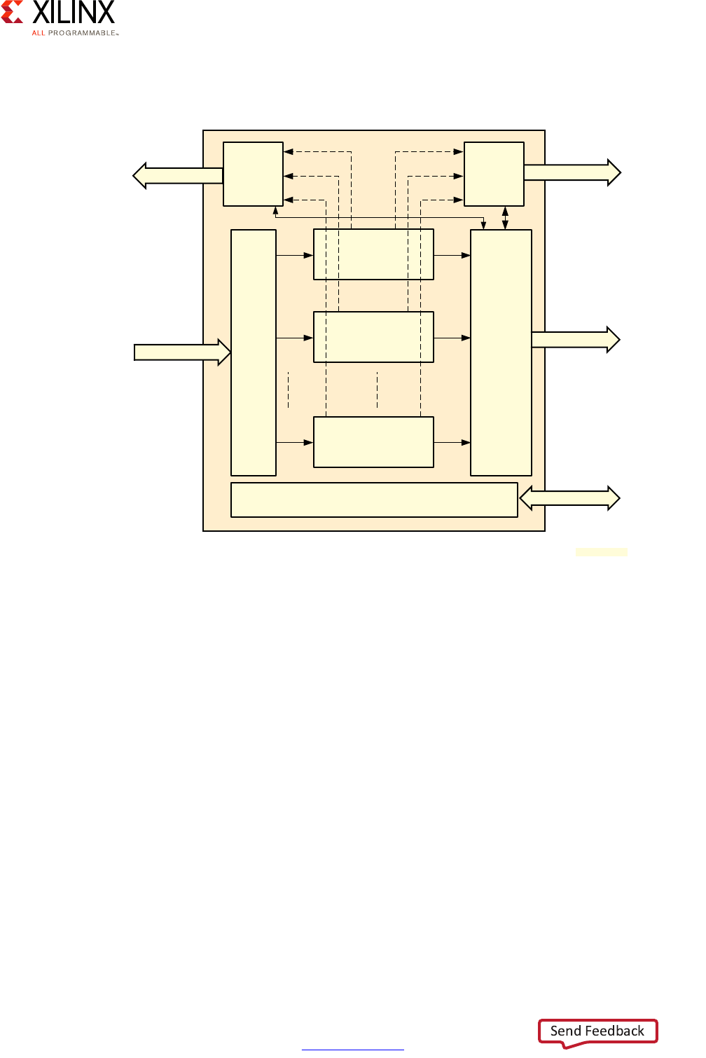
Zynq UltraScale+ MPSoC Embedded Design Methodology Guide 122
UG1228 (v1.0) March 31, 2017 www.xilinx.com
Chapter 6: Memory
The following diagram illustrates the internals of each of the general purpose DMA
controllers:
Simple DMA
In Simple DMA mode, transfer commands are issued to the controller as a single
instruction. This programming model for DMA requests can be summarized like this:
1. Data transfer source address destination address are programmed in a DMA channel
register.
2. The source’s size and destination buffers are programmed in the same channel register.
3. Interrupts are enabled in the channel if needed.
4. DMA transfer is started.
If interrupts are enabled, an interrupt will be generated when the DMA controller is done
reading the memory and another one will be generated once it is done writing to the
destination.
If a requested DMA read goes beyond the boundary of a memory page, the DMA controller
can optionally be instructed to fetch the data remaining up until that boundary. This is the
X-Ref Target - Figure 6-5
Figure 6-5: DMA Block Diagram
DMA
Channel 1
DMA
Channel 7
MUX
Common
Buffer
Read
Arbiter
Write
Arbiter
APB Registers APB
DMA
Channel 0
RDATA
AXI RD CMD AXI WR CMD
WDATA
X15366-092516

Zynq UltraScale+ MPSoC Embedded Design Methodology Guide 123
UG1228 (v1.0) March 31, 2017 www.xilinx.com
Chapter 6: Memory
OverFetch feature. When this feature is disabled, requests for incomplete memory pages
are completed using multiple single byte reads.
The simple DMA mode also has two sub-modes:
• Read-only: In read-only mode, the DMA channel reads the data from the memory but
does not write it anywhere. This can be used to scrub the memory to correct potential
error-correcting code (ECC) errors.
• Write-only: In write-only mode, the DMA channel writes preloaded data from the DMA
channel registers to the memory. It’s a convenient way to quickly initialize a block of
memory.
Scatter-Gather DMA
Scatter-Gather DMA is a more complex mode of operation where the data source and data
destination are specified in formatted Buffer Descriptors (BDs). The DMA controller
supports three different descriptor formats, which can suit different needs:
• Linear: Linear BDs are stored as a linear array. Each 128 bit descriptor includes the
source address and destination address for a DMA transfer.
• Linked-List: Linked-List BDs are 256 bits wide and include the same information as the
linear descriptors, but they also include the next BD’s address, which can be located
anywhere in the memory.
• Hybrid: In hybrid mode the two types of BDs can be mixed. An interesting way to use
the two patterns together would be to use the linked-list BD only at the boundary of a
memory page while using linear BD in the rest of the page.
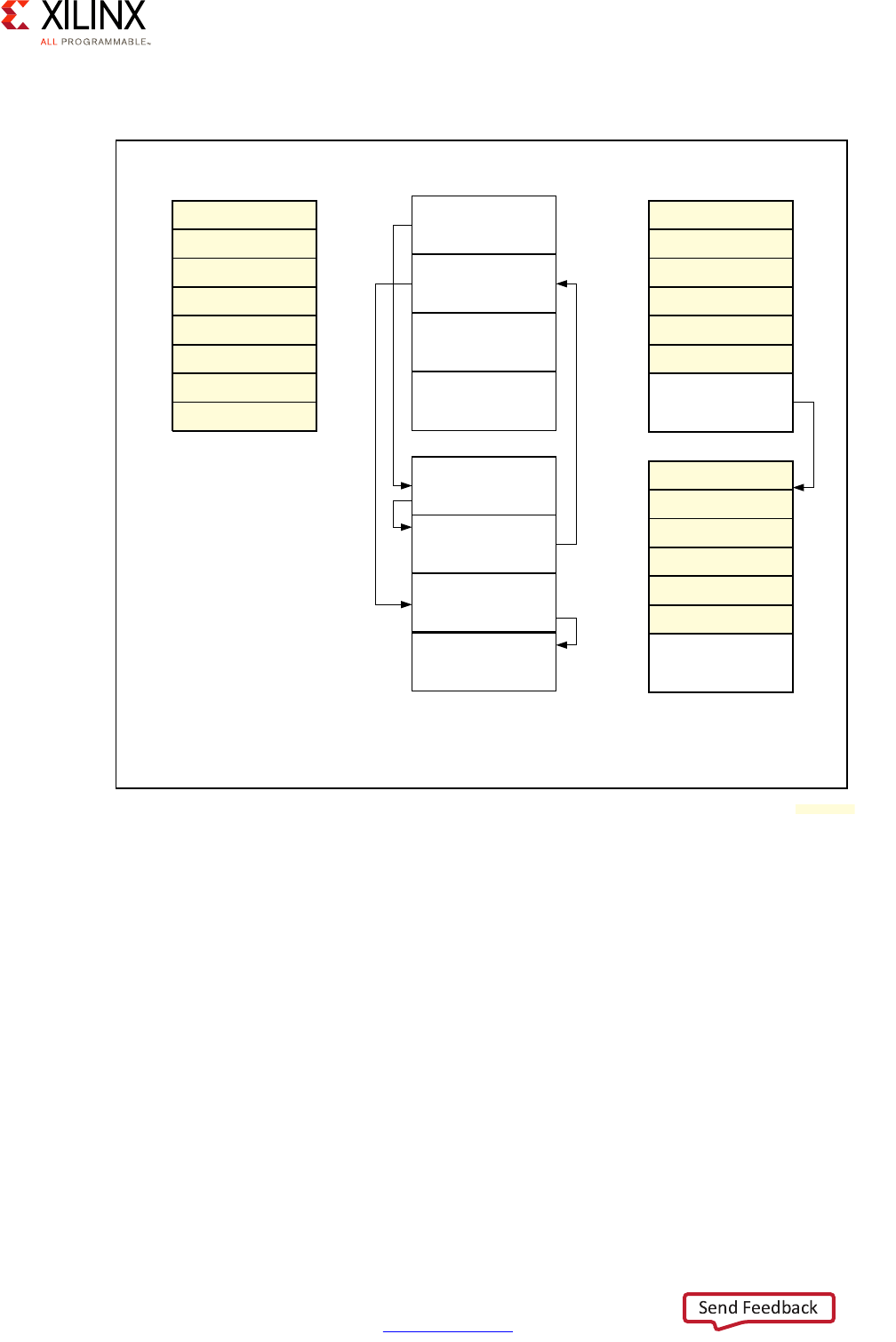
Zynq UltraScale+ MPSoC Embedded Design Methodology Guide 124
UG1228 (v1.0) March 31, 2017 www.xilinx.com
Chapter 6: Memory
The following figure illustrated these three formats.
Scatter-Gather DMA also supports interrupts. The number of generated interrupts is
maintained using a special accounting register. The register is incremented for each
descriptor handled by the DMA controller. Applications can consult the register to learn the
DMA transfer status and reset the register when needed.
Peripheral DMA
As mentioned earlier, the high-speed peripherals on the Zynq® UltraScale+™ MPSoC come
with their own DMA controllers. The characteristics of each peripheral DMA is specific to
each peripheral and will therefore be discussed in Chapter 10, Peripherals. The table below
summarizes the DMA-related information for each of the high-speed peripherals.
X-Ref Target - Figure 6-6
Figure 6-6: Supported Scatter-Gather Use Cases
Dscr0
Dscr1
Dscr2
Dscr3
Dscr4
Dscr5
Dscr6
Dscr7
Dscr0
Dscr1
Dscr2
Dscr3
Dscr4
Dscr5
Dscr6
Next Addr
Dscr3
Next Addr
Dscr0
Next Addr
Dscr7
Dscr8
Dscr13
Next Addr
Dscr5
Next Addr
Dscr4
Next Addr
Dscr2
Next Addr
Dscr1
Next Addr
Linear Descriptor Mode Linked-List Descriptor Mode Hybrid Descriptor Mode
128-bit Descriptor
Descriptor Element
Type = 0
256-bit Descriptor
Descriptor Element
Type = 1
128 and 256-bit Descriptor
Descriptor Element Type = 0 and 1
Linked-List Descriptor is Only
Used on Page Boundary
X15368-092516
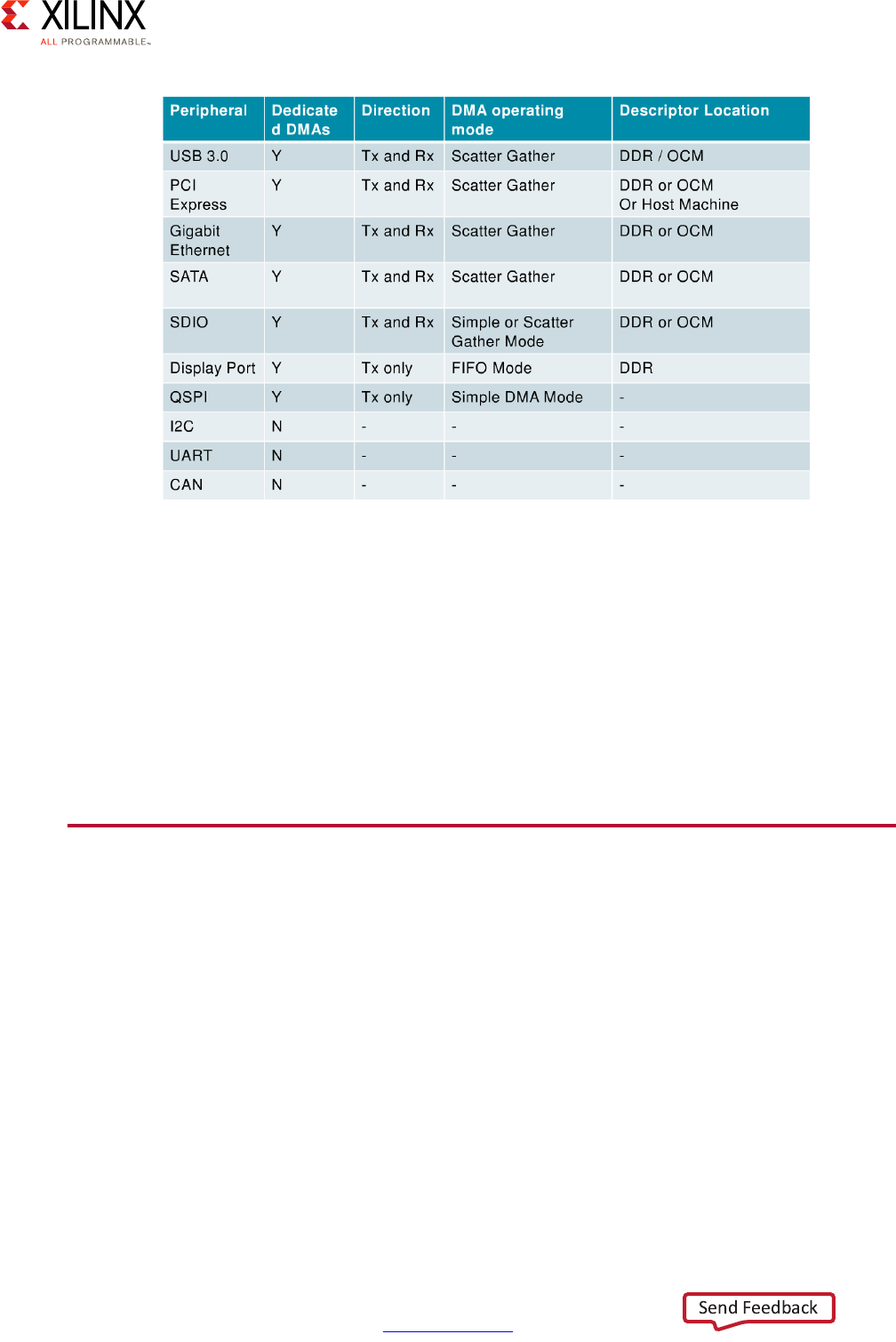
Zynq UltraScale+ MPSoC Embedded Design Methodology Guide 125
UG1228 (v1.0) March 31, 2017 www.xilinx.com
Chapter 6: Memory
Use and Programming
Typically, the OSes and/or drivers running on any of the processing units, which are
discussed in Chapter 2, Processing System, program and interface the various DMA
controllers. Hence, analyzing how to best use the DMAs and partition their resources
should likely be part of your overall software design. Furthermore, keep in mind that the
DMA controllers are AXI masters like many other components on the AXI bus. Prioritizing
DMA traffic is therefore possible using the same techniques discussed for tweaking QoS in
Chapter 2.
External Memory with the PL
As outlined earlier, it’s possible to use the Zynq UltraScale+ MPSoC device’s PL to interface
with external DDR memory. This is possible using a special IP block generator provided by
Xilinx. The Memory Interface Generator (MIG) generates the required blocks to be
integrated in the FPGA PL fabric. The MIG can generate interfaces for several types of
dynamic RAM:
• DDR3/DDR4
•QDR II+
•QDR-IV
•RLDRAM
X-Ref Target - Figure 6-7
Figure 6-7: Peripherals DMA Support
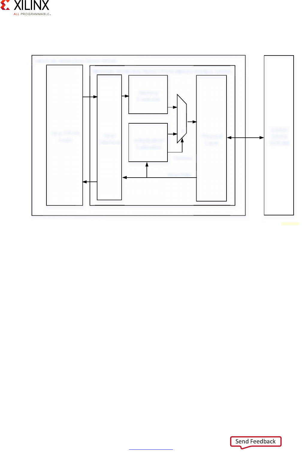
Zynq UltraScale+ MPSoC Embedded Design Methodology Guide 126
UG1228 (v1.0) March 31, 2017 www.xilinx.com
Chapter 6: Memory
In the case of DDR3 and DDR4, the MIG generates a structure similar to the one illustrated
here:
The Physical Layer (PHY) handles the low-level signals required by the DDR memory to
work. It deals with calibration and generates the precisely timed signals needed to read and
write to memory. It also deals with RAM initialization on power-up. The Memory Controller
(MC) handles the write/read transaction requests from the user interface and routes them
to the physical layer. It also handles the memory ECC feature if necessary.
The MIG can thus allow developers to access additional external memory through the PL
block. This can be used to enable the PL to use memory independently of the rest of the
system or it can be adapted to allow the external memory to be shared with other
components. The Video Codec Unit (VCU) built into the PL, for instance, can be made to use
the extra memory made available by a soft DDR controller. Another use of extending the
memory through the PL is, as was explained earlier, for achieving even higher external
memory access bandwidth than the Zynq UltraScale+ MPSoC device’s maximum
19,200MB/s available through its PS DDR controller.
X-Ref Target - Figure 6-8
Figure 6-8: Typical Blocks Generated by Memory Interface Generator
User FPGA
Logic
A
User
Interface
Memory
Controller
Initialization/
Calibration
Physical
Layer
DDR3/
DDR4
SDRAM
UltraScale Architecture-Based FPGAs
UltraScale Architecture-Based FPGAs Memory Interface Solution
CalDone
Read Data
1
0
;
Zynq UltraScale+ MPSoC Embedded Design Methodology Guide 127
UG1228 (v1.0) March 31, 2017 www.xilinx.com
Chapter 7
Resource Isolation and Partitioning
As a heterogeneous computing device, the Zynq® UltraScale+™ MPSoC device contains
several processing blocks, peripherals and memory types. The ability to group these
resources together, and partition and isolate those groups from one another is a key feature
of the Zynq UltraScale+ MPSoC device. This enables designers to create independent
subsystems that have access to the hardware resources they require while remaining
protected from one another and therefore immune from inter-subsystem attacks.
Furthermore, the Zynq UltraScale+ MPSoC device's processing blocks provide several
intra-subsystem security mechanisms to enable partitioning and isolation within any
designated subsystem. This chapter covers the Zynq UltraScale+ MPSoC device's resource
isolation and partitioning mechanisms along with the recommendations for their use.
Defining Your Resource Isolation and Partitioning
Needs
The first step in defining your resource isolation and partitioning needs is understanding
the Zynq UltraScale+ MPSoC device's core components, their interrelation and their typical
uses. This chapter therefore assumes that you have at least first read Chapter 2, Processing
System, Chapter 3, System Software Considerations, and Chapter 6, Memory. As we will see
shortly, the Zynq UltraScale+ MPSoC device's resource isolation and partitioning
capabilities are very flexible. The guiding principle to their use should be a clear definition
of independent yet co-existing divisions within your design that can be more or less clearly
identified as co-existing subsystems with complementary functionality that may or may not
need to be fully or partially isolated or protected from one another.
To help you in this task, we suggest you start by answering the following questions:
• What are the main workload divisions in your design between the main Zynq
UltraScale+ MPSoC device components as identified in Chapter 2, Processing System?
In other words, what do you envision running on the application processing unit (APU)
vs. the real-time processing unit (RPU) vs. processing logic (PL)?
• Can those separate workloads be grouped into distinct, clearly-identifiable
subsystems? Or, alternatively, can you identify distinct subsystems within your design
based on the Zynq UltraScale+ MPSoC device's heterogeneous computing capabilities?

Zynq UltraScale+ MPSoC Embedded Design Methodology Guide 128
UG1228 (v1.0) March 31, 2017 www.xilinx.com
Chapter 7: Resource Isolation and Partitioning
• Do you need to simultaneously host distinct execution environments (i.e. subsystems)
in parallel on the Zynq UltraScale+ MPSoC device while still enforcing strong isolation
between them? For example, would you like to:
°Isolate run-time environments on the APU?
°Isolate the work done on the APU from that done on the RPU?
• Do you need to restrict or control access to certain peripherals and/or memory based
on which subsystem they belong to in your design? For example, would you like to
ensure that:
°Only the APU has access to the DisplayPort?
°Only the RPU has access to the controller area network (CAN bus)?
°Certain sections of RAM are only available to the RPU?
Resource Isolation and Partitioning Methodology
Understanding the Zynq UltraScale+ MPSoC device's resource isolation and partitioning
capabilities and how best to use them involves covering several system components. As
with other chapters, this methodology section will present you key concepts required to
understand the in-depth explanations outlined in later sections. In doing so, this will help
you better understand if and how you can divide your design into independent, protectable
subsystems, even if the answers to the previous section's questions were unclear to you at
first.
The resources and blocks of the Zynq UltraScale+ MPSoC device were presented earlier in
this guide in several different ways. For the present discussion, we will group the Zynq
UltraScale+ MPSoC device parts relevant to resource isolation and partitioning under three
broad categories as you can see in the following diagram.
Note: The categories and accompanying diagrams below do NOT attempt to precisely represent the
internal blocks of the Zynq UltraScale+ MPSoC device. Instead, they are primarily a conceptual view
for the purposes of the present explanation.
Zynq UltraScale+ MPSoC Embedded Design Methodology Guide 129
UG1228 (v1.0) March 31, 2017 www.xilinx.com
Chapter 7: Resource Isolation and Partitioning
The three categories illustrated above can be described as:
• Processing blocks and general-purpose direct memory access (DMA)
Includes all blocks that initiate and control most accesses, transfers and communication
around the Zynq UltraScale+ MPSoC device.
• Peripherals
Includes all peripherals from all power domains; mainly Low-Power Domain (LPD) and
Full-Power Domain (FPD), as well all peripherals built into the PL.
•Memory
Includes all memory blocks within and accessible by the Zynq UltraScale+ MPSoC
device.
The arrows indicate the typical direction by which access is initiated. The various processing
blocks and general-purpose DMAs are generally interfacing with peripherals or memory to
carry out their designated workloads. Peripherals on the other hand most often need to
interface with memory for I/O purposes. Memory banks do not themselves initiate any
communication.
More specifically, the arrows indicate the direction of the AXI traffic. Recall that, as
described in Chapter 2, Processing System, the Zynq UltraScale+ MPSoC device's internal
interconnect is based on several ARM standards, the core concept of which are endpoints
called AXI masters and AXI slaves; the AXI masters initiating read and write requests while
AXI slaves respond to those requests. Hence the arrow from the processing blocks and
X-Ref Target - Figure 7-1
Figure 7-1: Basic View of Zynq UltraScale+ MPSoC Device Resources and their Interactions
P
er
iph
era
l
s
P
rocess
i
n
g
Bl
oc
ks
&
G
eneral-Pur
p
ose DMA
M
emor
y
* GPU support is OS-specific
TCM
D
DRC
Memory
y
OC
M
F
PD
Peripherals
PL
Peripherals
LPD
Peripherals
RPU
PL
GPDMA
APU
GP
U
*
PL
/
M
IG
X18702-032917
Zynq UltraScale+ MPSoC Embedded Design Methodology Guide 130
UG1228 (v1.0) March 31, 2017 www.xilinx.com
Chapter 7: Resource Isolation and Partitioning
general-purpose DMA to the peripherals indicates that the traffic is initiated by the former's
AXI masters to the latter's AXI slaves. Typically, this type of access allows a processing block
to access a peripheral's control registers and/or request specific operations from the
peripheral. As is discussed in Chapter 10, Peripherals, most Zynq UltraScale+ MPSoC device
peripherals also have DMA-capable AXI masters for enabling those peripherals, once
programmed accordingly by the processing blocks, to interact with memory to transfer data
to or from the peripheral. This is illustrated by the arrow going from the peripherals to the
memory.
Note that the GP DMA block included with the processing blocks encompasses the
low-power domain general-purpose DMA controller as well as the full-power domain
general-purpose DMA controller covered in Chapter 6, Memory. Both are actually
programmable through their AXI slave ports as an LPD peripheral and an FPD peripheral
respectively. Again, this diagram's purpose is to help contextualize the Zynq UltraScale+
MPSoC device's capabilities. Refer to Chapter 2, Processing System for the complete
interconnect diagram.
Within the Zynq UltraScale+ MPSoC device, the three main boundaries illustrated above are
protected by three complementary protection mechanisms as is illustrated below:
X-Ref Target - Figure 7-2
Figure 7-2: Zynq UltraScale+ MPSoC Device Resources and Protection Mechanisms
XMPU
XMPU
XPPU
SMMU
SMMU
P
er
iph
era
ls
P
rocess
i
n
g
Bl
oc
ks
&
G
eneral-Pur
p
ose DM
A
Memor
y
SMMU
FPD
P
er
iph
era
ls
LPD
P
er
iph
era
ls
PL
P
er
iph
era
ls
GPDMA
XMPU
RPU
PL
G
P
U
*
APU
XPPU
* GPU support is OS-specific
T
CM
OCM
PL
/
MI
G
D
DR
C
M
emor
y
X18704-032917
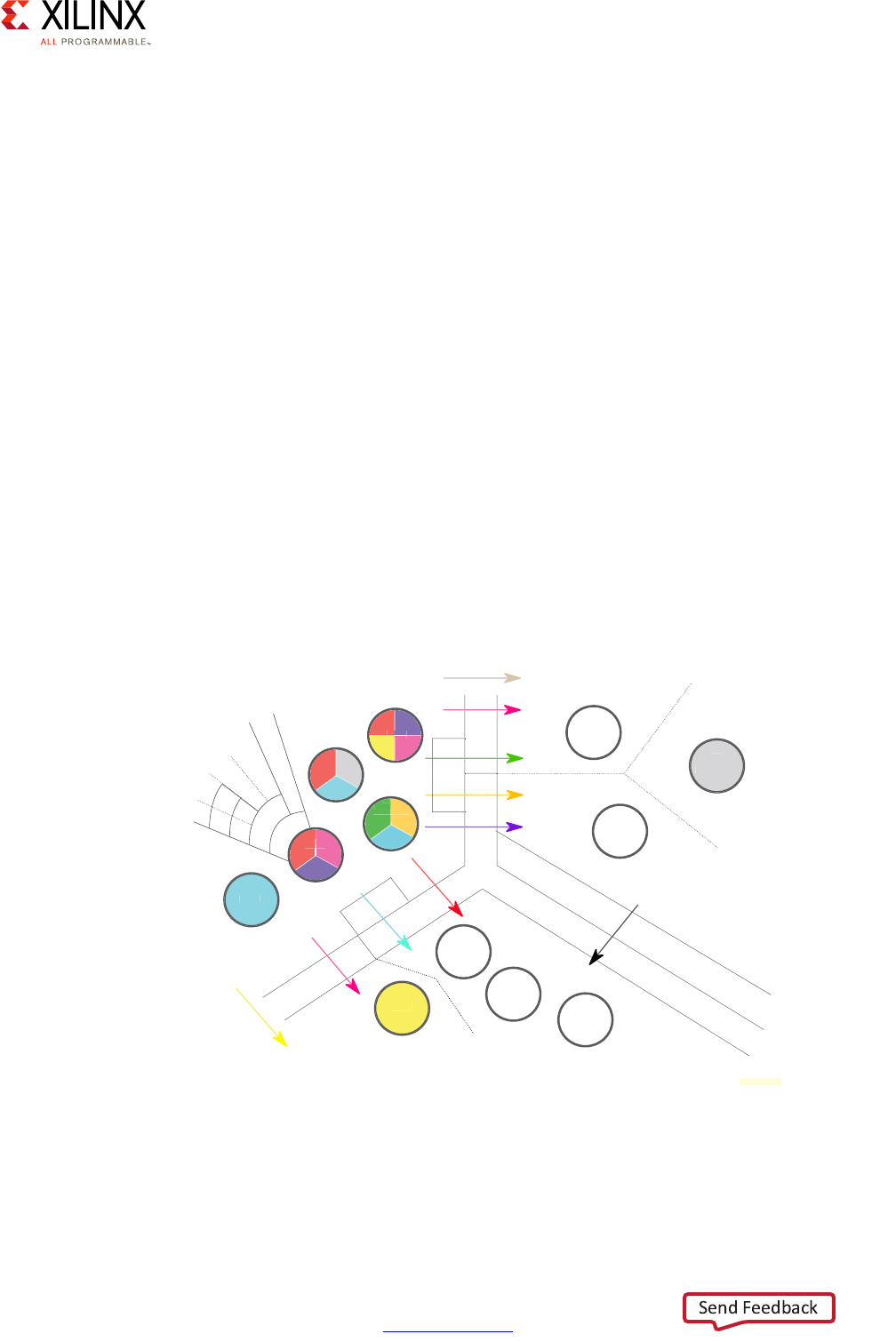
Zynq UltraScale+ MPSoC Embedded Design Methodology Guide 131
UG1228 (v1.0) March 31, 2017 www.xilinx.com
Chapter 7: Resource Isolation and Partitioning
The System Memory Management Unit (SMMU), the Xilinx® Memory Protection Unit
(XMPU) and the Xilinx Peripheral Protection Unit (XPPU) fulfill complementary roles in
enabling system designers to isolate and partition resources. Namely:
• The SMMU, described in Chapter 2, Processing System, allows DMA capable devices to
reference virtual addresses. These virtual addresses can be mapped by the SMMU
directly to the virtualized physical addresses expected by a hypervisor guest, or to real
physical addresses utilized by an operating system running natively on the APU.
• The XMPU, which is covered in greater detail in Xilinx Memory Protection Unit,
page 142, enables the filtering of access to memory and FPD peripherals based in part
on the ID of the AXI master which makes the access request.
• The XPPU, which is covered in Xilinx Peripheral Protection Unit, page 145, enables the
filtering of access to LPD peripherals based in part on the ID of the AXI master which
makes the access request.
As illustrated above, there can be several combinations of those three protection
mechanisms and they are not used in all paths between processing blocks, peripherals and
memory. The interconnect diagram presented in Chapter 2, Processing System provides the
full details of the involvement of the protection mechanisms along the paths between the
various Zynq UltraScale+ MPSoC device blocks. The following diagram provides a summary
of those interactions for the present discussion's purposes:
In the above diagram, like-colored arrows are used by or for similarly-colored components.
Take the RPU for example. It contains a pink quadrant that indicates that it uses the pink
arrow, through the XPPU, to access LPD peripherals. To get to the yellow TCM, however, the
X-Ref Target - Figure 7-3
Figure 7-3: Detailed Isolation and Partitioning Paths
XMPU
XMPU
XPPU
SMMU
SMMU
P
er
iph
era
l
s
P
rocess
i
n
g
Bl
oc
k
s
&
G
eneral-Pur
p
ose DMA
Memor
y
O
CM
T
C
M
D
DRC
M
emor
y
MM
SMMU
F
PD
P
er
iph
era
ls
LPD
P
er
iph
era
ls
PL
P
er
iph
era
ls
D
DMA
D
GPD
XMPU
U
RPU
RP
PU
RP
PU
P
PL
L
P
TrustZone
Secure
Non-Secure
Linux
nu
Apps
App
P
1
P2
P3
P4
GPU
*
Xen
P
PU
AP
XPPU
* GPU support is OS-specific
PL/MIG
X18703-032917

Zynq UltraScale+ MPSoC Embedded Design Methodology Guide 132
UG1228 (v1.0) March 31, 2017 www.xilinx.com
Chapter 7: Resource Isolation and Partitioning
RPU's yellow quadrant indicates that is uses the yellow arrow, without passing through any
of the SMMU, XMPU or XPPU. That is because the TCM is collocated within the RPU even
though it's accessible to the rest of the system through the global memory map described
in Chapter 6, Memory. The APU's access to the TCM, on the other hand, follows a similar
path as the APU's access to the LPD peripherals, using a pink arrow through the XPPU.
Without going into every possible path in detail, there are some important observations to
make while looking at this diagram; bearing in mind that, as before, the arrows indicate the
direction of AXI traffic, from AXI masters to AXI slaves.
First and foremost, notice how the XMPU and the XPPU are present in the path of the
majority of interactions. The only exceptions to this are interactions between internal
components of the same subsystem: the TCM being part of the RPU and the PL peripherals
being part of the PL. Save for those exceptions, all interactions, even within a given power
domain, are subject to whatever rules are set up in the XMPU and the XPPU. While the APU
and the FPD peripherals are all part of the full-power domain, for instance, all interactions
between the two go through the XMPU. Similarly, despite the RPU and LPD peripherals both
being part of the lower-power domain, their interactions all go through the XPPU. In short,
by properly configuring the XMPU and the XPPU you can essentially control all interactions
occurring in the system at any time.
Second, notice the role of the SMMU. It's involved in all cases where the general purpose
DMAs are used or if the peripherals need to interact with the memory. As explained earlier,
and as detailed in Chapter 2, Processing System, the SMMU enables two stage address
translation for the DMA-capable devices when used by native (i.e. non-virtualized) OSes as
well as address virtualization for I/O and hypervisor use. When the SMMU is used in a
non-virtualized environment, it ensures that devices can only access addresses designated
for them. In a virtualized scenario, the SMMU additionally ensures that device addresses are
correctly mapped to the memory space used by a guest OS running on the APU. In other
words, a guest OS does not explicitly program a peripheral DMA with an actual physical
address. Instead, the fact that all peripherals accesses go through the SSMU before
reaching memory ensures the proper translation between the address provided by the
guest OS and the one used by the peripheral.
Third, note that the APU further provides additional mechanisms for isolating and
partitioning the software running on it. At the lowest level, TrustZone allows partitioning
the APU between secure and non-secure execution environments. As we will see below, the
secure/non-secure state is communicated across AXI transactions and can be used by the
XMPU/XPPU to discriminate requests accordingly. Also, as discussed in Chapter 3, System
Software Considerations chapter, the A53 cores within the APU can further be subdivided
between different guests using a hypervisor such Xen. Alternatively, as also covered in
Chapter 3, the A53 cores can be directly managed in symmetric multiprocessing (SMP)
mode using an OS such as Linux. Whether a hypervisor is used or not, any high-level OS
would then typically rely on the A53s' memory management unit (MMU) to isolate and
protect processes against each other and the OS against the user-space processes.
Zynq UltraScale+ MPSoC Embedded Design Methodology Guide 133
UG1228 (v1.0) March 31, 2017 www.xilinx.com
Chapter 7: Resource Isolation and Partitioning
Finally, note that the rules for the PL and its peripherals are to an extent configurable. When
accessing memory, for instance, the PL may or may not go through the SMMU depending
on the AXI port being used from the PL side. Also, the peripherals within the PL aren't
available from components outside the PL by default. You must configure the PL IP to that
effect and can, therefore, add any AXI filtering rules in the IP that you deem appropriate. An
example of this will be given shortly.
By combining these mechanisms together, you can effectively subdivide your design into
independent subsystems as explained earlier. The following diagram illustrates such an
example subdivided design:
In this illustration of the use of the Zynq UltraScale+ MPSoC device's protection
mechanisms, the design is divided amongst three independent subsystems. Each of the
subsystems contains a separate processing block that acts as the primary processing agent
within that block for interacting with that subsystem's peripherals. Note that both
subsystems A and B contain peripherals belonging to power domains other than the one to
which belongs that subsystem's processing block(s). The APU in subsystem A, for instance,
belongs to the full power domain. Still, using the XPPU, we are able to carve out exclusive
access for the APU for peripherals belong to the low power domain, namely USB, eMMC
and Ethernet. The same occurs in subsystem B where the RPU, belonging to the low power
domain, has exclusive access over the SATA interface that belongs to the full power domain.
Therefore the use of power domains as presented in Chapter 4, Power Considerations does
not interfere with the Zynq UltraScale+ MPSoC device's resource isolation and partitioning
capabilities.
In this example, subsystem A's peripherals are off-limits to subsystem B and vice-versa.
Subsystem A can't, for instance, access the SATA interface reserved to subsystem B.
X-Ref Target - Figure 7-4
Figure 7-4: Example Subsystem Isolation and Partitioning
Subsystem A
APU
GP
U
Processing
Peripherals
Low-Power
Domain
Full-Power
Domain
US
B
eMM
C
PC
I
e
Di
sp
l
a
y
Po
r
t
E
th
e
r
-
n
et
Subsystem B
RPU
Processing
Peripherals
Low-Power
Domain
Full-Power
Domain
O
CM
C
AN
S
AT
A
G
PI
O
Subsystem C
PL
P
er
iph
era
l
s
PL
X18705-032117

Zynq UltraScale+ MPSoC Embedded Design Methodology Guide 134
UG1228 (v1.0) March 31, 2017 www.xilinx.com
Chapter 7: Resource Isolation and Partitioning
Conversely, subsystem B can't access the Display Port which is reserved to subsystem A.
These enforcements happen at the level of the interconnect whose configurations can be
set as read-only immediately at boot time. This architecture therefore presents very high
barriers to adversaries who might seek to gain unwanted access to system resources. There
are no means for software running on the APU, for instance, to modify these rules at
runtime. For all intents and purposes, the Zynq UltraScale+ MPSoC device's isolation and
partitioning capabilities enable you to divide subsystem A and subsystem B as if they were
physically separate devices.
A similar level of protection is given to subsystem A and B from subsystem C. The protection
of subsystem C from subsystems A and B is, however, a bit different. In the PL's case there
is no XMPU or XPPU leading into the PL block. Instead, the PL IP can be configured to filter
incoming traffic to the PL's AXI slave ports based on the AXI master's ID. In other words, as
the designer, you can block any AXI traffic coming into a given PL AXI slave port based on
the identity of the AXI block making the request. You can, for instance, make a certain AXI
slave port on the PL respond exclusively to the APU. Any requests on that AXI slave coming
from the RPU would therefore be refused. In short, by customizing the PL's IP, you can
effectively implement the same, if not more stringent, controls than those afforded by the
XMPU and the XPPU to the other components of the Zynq UltraScale+ MPSoC device.
There exists many more example scenarios as the one outlined above. Deciding whether
your design needs to be subdivided in such a fashion and how to go about doing that is
going to be specific to your requirements and specifications. There are no specific
established rules to follow, except, as we suggested earlier, that you take the time to clearly
identify the subdivisions in your system and understand how to use the Zynq UltraScale+
MPSoC device's capabilities to achieve the underlying design goals.
Still, integrating the Zynq UltraScale+ MPSoC device's resource isolation and partitioning
capabilities into your design will certainly contribute to its increased security. By
familiarizing your team with these capabilities early, you will be able to continuously tweak
them as required. Should you decide not to use these capabilities, you can always revisit
that decision later. Bear in mind, however, that trying to retrofit security constraints is often
increasingly difficult as a system's implementation progresses. Hence, if security is one of
your requirements or likely to be considered one during your project's lifetime, we strongly
recommend you consider further investigating the material covered by this chapter in
earnest.

Zynq UltraScale+ MPSoC Embedded Design Methodology Guide 135
UG1228 (v1.0) March 31, 2017 www.xilinx.com
Chapter 7: Resource Isolation and Partitioning
ARM TrustZone
ARM's TrustZone technology and the concepts underlying it are an important part of
several of the Zynq UltraScale+ MPSoC device's features. As was alluded to earlier, the
XMPU and XPPU, for instance, can filter access based on the secure state defined in ARM
TrustZone. For a number of reasons, unfortunately, TrustZone can be a difficult topic to
approach, even for experienced teams. Having a solid understanding of TrustZone and how
it fits in the Zynq UltraScale+ MPSoC device's overall functionality with regards to your
design is nonetheless important. This section's aim is to help guide you with regards to
TrustZone, its uses within the Zynq UltraScale+ MPSoC device and how you can customize
your design around it.
TrustZone Basics
To understand what TrustZone does, we must take a step back and look at how modern-day
processors separate privileges. In most modern processor designs, the are typically at least
two modes of operation: privileged and unprivileged. The privileged mode is used by OSes
whereas the unprivileged mode is used by regular applications. Processors typically have
operands and registers that can only be used in the privileged mode, thereby granting an
OS greater control over the system over the processor's configuration. Such separation is
further enforced by the processors' MMUs thereby ensuring that OSes are protected from
unauthorized accesses by unprivileged applications.
This separation scheme between privileged and unprivileged mode is found across process
architectures and is sometimes referred as "kernel-space vs. user-space" in the software
world. In other circumstances, the OS can be referred to as running in "ring 0"; an allusion
to the fact that there might be several privilege "rings" with the OS being the innermost
ring. Whereas the concepts can have different names, such division had historically been
sufficient for most applications.
Recently, however, general-purpose processors, such as the ARM architecture, have
increasingly been used in applications where even the general-purpose OSes they are
running can't be trusted for isolating certain software workloads from the rest of the
system. Indeed, modern-day OSes have become very complex and it is not uncommon to
have security fixes be issued for them on a regular basis. Yet, increasingly, designs require
secure functionality, such as for securing user credentials or decrypting DRM-encoded
media, to coexist with general-purpose OSes on the same processor.
The purpose of ARM's TrustZone technology is to address this need by defining yet another
privilege level underneath that of the general-purpose OS being run on the processor. With
TrustZone, the OS running on the ARM processor no longer has the highest set of
privileges. Instead, there is another software level that has even more privileges than the
OS, thereby enabling important operations to be conducted outside the context of the OS
or its applications in a secure fashion. Using TrustZone, these operations and the entire
secure context, in fact, are transparent to the OS. In other words, the general-purpose OS

Zynq UltraScale+ MPSoC Embedded Design Methodology Guide 136
UG1228 (v1.0) March 31, 2017 www.xilinx.com
Chapter 7: Resource Isolation and Partitioning
running on a TrustZone-capable ARM processor actually thinks it has full control over the
processor, very much as if TrustZone wasn't there. While, still, TrustZone continues to
operate and offer its services as required.
Much like the OS has access to special processor functionality and registers, and the ability
to configuration memory protection mechanisms to protect itself from regular applications,
so too does the additional privilege level defined by TrustZone have access to special
features of ARM processors to ensure that it can provide an isolated secure context. This
means that the state of the processor, including register values, as seen by the non-secure
world (i.e. the regular OS and its applications) must be preserved when entering secure
state and restored when returning back to non-secure state. This also means that once the
non-secure state has been saved, the processor can be made to run an entirely separate, yet
secure stack from the non-secure, general-purpose OS and its applications. That secure
stack is invisible to the latter.
To communicate with the secure software stack, a general-purpose OS running on
TrustZone will typically have a driver, or a set of drivers, for calling into the secure context
using interrupts. Applications use those drivers as if they were communicating with any
regular device. The OS itself simply uses the available processor capabilities to trigger
interrupts when requested to do so by the drivers. The only difference is that those
interrupts are caught by the TrustZone security context instead of being caught by the OS'
interrupt service routines as would typically occur. Those interrupts are then serviced by the
secure context in whichever way the software operating there has been programmed to do.
Exception Levels
TrustZone as implemented on the APU's ARMv8 A53s builds on the basic concepts we just
explained and defines 4 privilege levels, each being called a separate exception level (EL), as
illustrated in the following figure.
Zynq UltraScale+ MPSoC Embedded Design Methodology Guide 137
UG1228 (v1.0) March 31, 2017 www.xilinx.com
Chapter 7: Resource Isolation and Partitioning
First and foremost, notice how TrustZone enables the existence of a separate secure stack in
parallel to the main non-secure stack running on the A53s. For instance, in the non-secure
side Xen could be used as the hypervisor running at EL2 while Linux guest OS instances are
hosted by Xen at EL1, the latter themselves running applications at EL0. Yet, when EL3 is
entered, the software running there, and referred to above as secure monitor mode, could
spawn into a separate secure stack that also has a secure OS running at EL1 and secure
applications running at EL0.
Those software layers within the secure side are protected against each other in exactly the
same way as the software layers on the non-secure side are. In other words, the secure
applications running at EL0 can be protected from each other, and precluded from directly
accessing EL1 OS resources, in the same way that regular Linux applications running in the
non-secure context are protected from each other, and precluded from directly accessing
Linux kernel resources hosted in EL1.
Security Profile and Transaction Tagging
In addition to the APU being divided between secure and non-secure states, the Zynq
UltraScale+ MPSoC devices and configuration registers on the AXI interconnect follow the
same convention as TrustZone on the APU and can be secure, non-secure, both, or
configurable to be either. This is very important because all AXI memory transactions on the
interconnect are tagged as either being secure or non-secure. This state reflects whether
the origin of the transaction was secure or not, and can be used by the AXI slaves, as well as
the XMPU and the XPPU as mentioned above, to discriminate against non-matching parties.
X-Ref Target - Figure 7-5
Figure 7-5: TrustZone Exception Levels
Non-secure State
App1
AArch64 or
AArch32(1)
App2
AArch64 or
AArch32(1)
App1
AArch64 or
AArch32(1)
App2
AArch64 or
AArch32(1)
Supervisor (Guest OS1)
AArch64 or AArch32(2)
Supervisor (Guest OS2)
AArch64 or AArch32(2)
Hypervisor Mode
AArch64 or AArch32
EL0
EL1
EL2
SVC
HVC
SMC
Secure Monitor Mode
Supervisor (Secure OS)
AArch64 or AArch32
Trusted App1
AArch64 or
AArch32(1)
Trusted App2
AArch64 or
AArch32(1)
EL3
Secure State
X15288-032917

Zynq UltraScale+ MPSoC Embedded Design Methodology Guide 138
UG1228 (v1.0) March 31, 2017 www.xilinx.com
Chapter 7: Resource Isolation and Partitioning
Several key system components are secure AXI slaves. This includes the Platform
Management Unit (PMU), the Configuration Security Unit (CSU), as well as the System-Level
Control Registers (SLCRs). Hence, initiating communication with these components can only
be done by secure AXI masters. In the same way, some system components are secure AXI
masters. This includes the PMU and the CSU. Hence, the PMU and the CSU can initiated
secure AXI transactions between themselves at all times.
Also, all APU memory transactions initiated by an A53 operating in secure context will be
marked as secure on the AXI bus. This too is important to keep in mind as some key system
operations can only be conducted by secure code running on the APU. An A53 running in
secure context can therefore communicate with the PMU or the CSU while an A53 running
in non-secure context can't.
While in principle secure masters can access non-secure slaves, XMPU and XPPU
configurations can preclude non-secure slaves from being accessible from secure masters.
Refer to table 16-10 of the Zynq UltraScale+ MPSoC Technical Reference Manual (UG1085)
[Ref 7] for the full list of TrustZone profiles.
ARM Trusted Firmware
The Xilinx FSBL always boots the APU in secure mode and can be made to run the ARM
Trusted Firmware (ATF) as the Secure Monitor illustrated above running at EL3. The ATF was
introduced in Chapter 3, System Software Considerations and is part of the boot-time chain
of trust.
Among other things, the ATF is responsible for preserving and restoring the non-secure
context when switching to the secure context. It's also responsible for part of the
power-management since the PMU, which is responsible for power management, is a
secure AXI slave and will therefore not accept any commands issued by a hypervisor or
non-secure OS running on the APU. Power-management requests made by non-secure
OSes, such as Linux, are therefore proxied through the ATF to interact with the PMU.
Given its role in maintaining internal processor state within the A53s as well as mediating
between the APU and key system functionality and providing fundamental system security,
it's highly likely that your design will need to use ATF. This is especially true if you're running
Linux as was mentioned in Chapter 3, System Software Considerations.
Note: Xilinx does not support any configuration where an OS runs without an underlying ATF.
Trusted Execution Environment
While the ATF is crucial for operating the A53s, it doesn't in of itself provide the necessary
functionality and APIs for hosting custom secure applications such as those illustrated
above as running in secure mode at EL0 on to top right hand side of the diagram. That role
is typically filled by the component labeled as "Supervisor (secure OS)," which is known in
ARM literature as a Trusted Execution Environment (TEE).

Zynq UltraScale+ MPSoC Embedded Design Methodology Guide 139
UG1228 (v1.0) March 31, 2017 www.xilinx.com
Chapter 7: Resource Isolation and Partitioning
A TEE is not provided as part of the Xilinx system software stack. However, it is worth
describing here. The TEE is a separate software component from the ATF and whereas ARM
provides a reference open source ATF implementation, it relies on 3rd party partners for
providing TEEs. There are therefore several TEEs on the market and you will need to make a
determination as to whether you need one and, if so, which one you want to use. There is
at least one open-source TEE that support the Zynq UltraScale+ MPSoC device, the Open
Portable Trusted Execution Environment (OP-TEE) hosted at op-tee.org.
Each TEE defines its own API for writing secure applications and provides different means
and APIs for non-secure OSes and applications to communicate with it across the required
non-secure/secure context switches. When choosing a TEE, it's important to look at the APIs
and mechanisms it provides to make sure that they are appropriate for your project.
Feature Summary
Now that we've covered TrustZone's basics, its core functionality and the main supporting
software, the following feature highlight should be easier to appreciate:
• Critical devices such as the PMU, the CSU and the SCLRs are always secure, preventing
unauthorized access and modification of the security system itself.
• You can program devices to be either secure or non-secure.
• You can program memories, such as on-chip memory (OCM) and double data rate
(DDR), on a per-region basis to be secure or non-secure.
• The APU always boots in secure mode.
• The RPUs do not support the TrustZone technology, but you can configure each RPU to
emit transactions to the AXI bus as either a secure or non-secure master via the SCLRs.
For More Information
You can find out more about TrustZone in ARM's technical reference manual, and you can
more details about TrustZone's use and configuration in the Zynq UltraScale+ MPSoC
device at this link in the Zynq UltraScale+ MPSoC Technical Reference Manual (UG1085)
[Ref 7].
System Memory Management Unit
The purpose of the System Memory Management Unit (SMMU) is to complement the APU
cores' MMUs by ensuring that memory accesses generated by any component (i.e. AXI
master) programmed by software running on the APU are coherent with the mappings used
on the APU itself. Within the Zynq UltraScale+ MPSoC device, the SMMU is used to ensure
that all DMA accesses are properly translated to ensure isolation.
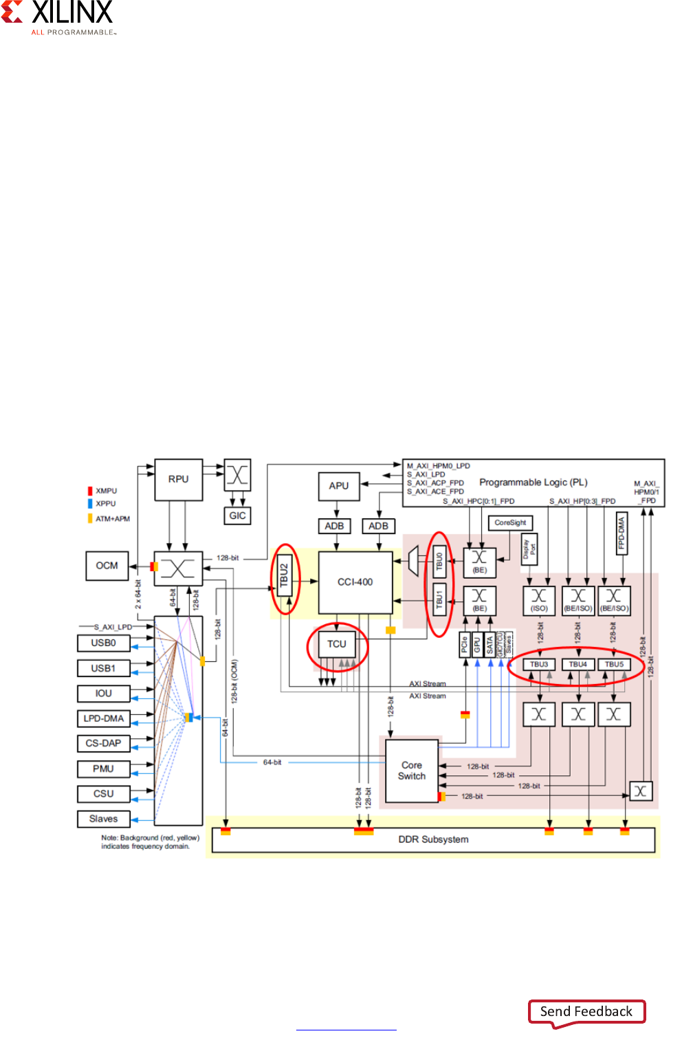
Zynq UltraScale+ MPSoC Embedded Design Methodology Guide 140
UG1228 (v1.0) March 31, 2017 www.xilinx.com
Chapter 7: Resource Isolation and Partitioning
This includes the DMA accesses from:
• LPD and FPD peripherals
• Software configurable DMA channels (i.e. general-purpose DMAs)
• Custom DMA-capable IP in Programmable Logic (PL)
The SMMU therefore helps protect the system against incorrectly programmed or malicious
devices corrupting the system memory or causing a system failure.
The SMMU's key components are:
• Translation Buffer Unit (TBU): Contains a translation look-aside buffer (TLB) that caches
page tables. The SMMU implements a TBU for each connected master. This helps
isolate devices in a virtual environment attempting to access common memory.
• Translation Control Unit (TCU): Controls and manages the address translations.
The following figure shows where the SMMU components are located across the
interconnect:
X-Ref Target - Figure 7-6
Figure 7-6: SMMU Component Locations in Interconnect
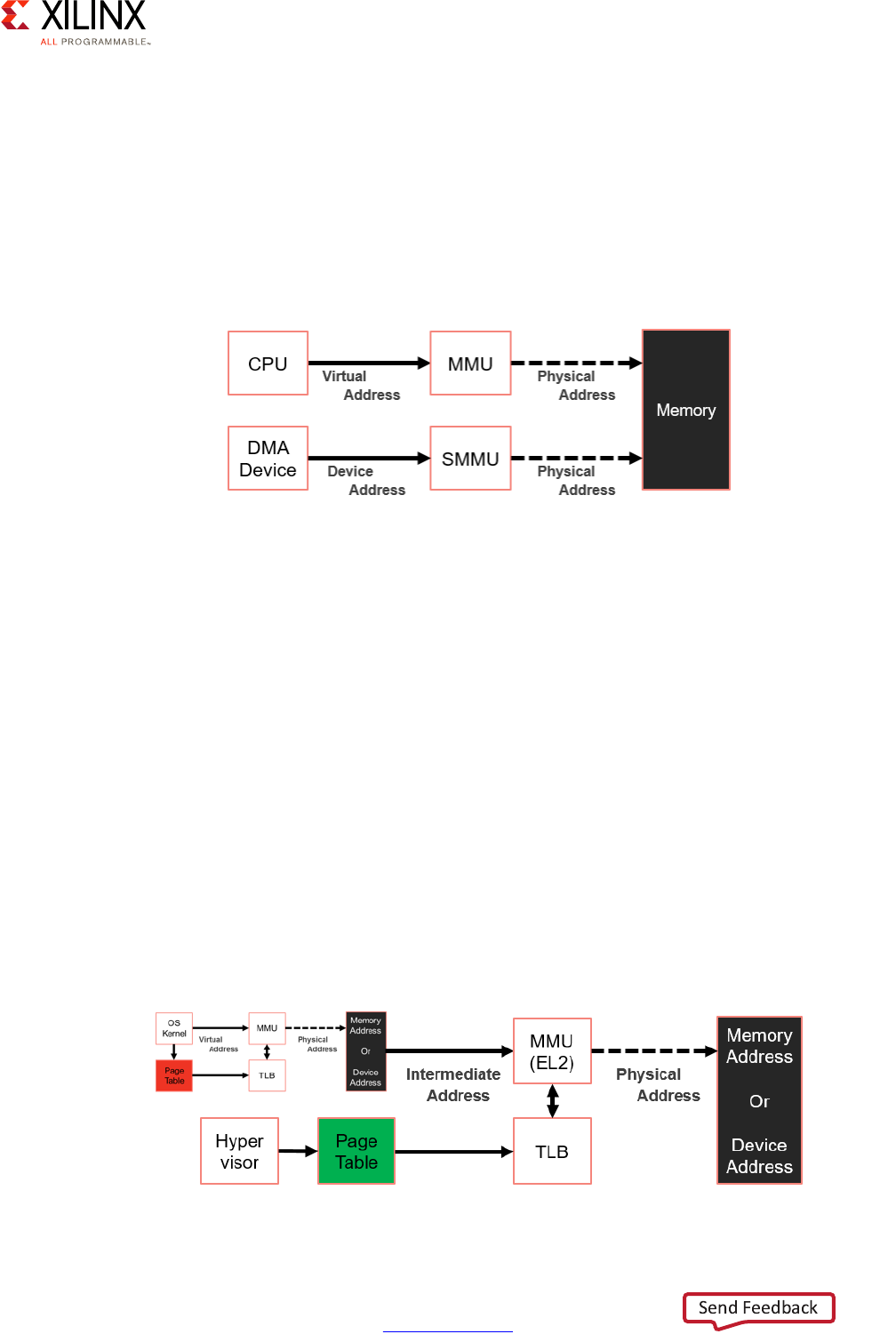
Zynq UltraScale+ MPSoC Embedded Design Methodology Guide 141
UG1228 (v1.0) March 31, 2017 www.xilinx.com
Chapter 7: Resource Isolation and Partitioning
Address Translation in Native Scenarios
For systems that are native (non-virtualized), the SMMU can provide address translation for
peripherals. This translation results in device isolation that prevents DMA attacks by
restricting DMA-capable peripherals to a pre-assigned physical space. Without this
memory isolation, peripherals could corrupt system memory. The following figure
illustrates how the SMMU is used in a native environment to allow the OS running natively
on the APU to control what memory any device (i.e. peripheral) DMA master can access:
Note that there is no requirement to use the SMMU in a native environment. However, using
it will certainly increase your system's security.
Global Isolation in Virtualized Scenarios
For systems that are virtualized, the SMMU is especially useful as it ensures that DMA
accesses requested by guest OSes are isolated from one another. This therefore prevents
malfunction, faults, or hacks in one domain from impacting other domains, thereby
providing system integrity in a virtualized environment. To that end the SMMU provides
capabilities for setting up appropriate translation regimes and context (I/O Virtualization).
The SMMU supports address translation regimes that require a two-stage translation
process in a virtualized environment in which a hypervisor is managing multiple guest OSes
and where the OSes are running multiple applications possibly attempting to access the
same system resources. The following figure illustrates how this translation occurs
independently from the guest OSes.
X-Ref Target - Figure 7-7
Figure 7-7: SSMU Usage in Native (Non-Virtualized) Configuration
X-Ref Target - Figure 7-8
Figure 7-8: SMMU Usage in Virtualized Configuration
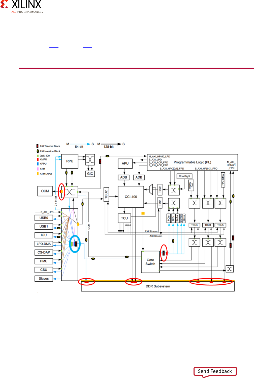
Zynq UltraScale+ MPSoC Embedded Design Methodology Guide 142
UG1228 (v1.0) March 31, 2017 www.xilinx.com
Chapter 7: Resource Isolation and Partitioning
Additional Information
Refer back to Chapter 2, Processing System for additional information about the SSMU as
well as this link and this link in the Zynq UltraScale+ MPSoC Technical Reference Manual
(UG1085) [Ref 7].
Xilinx Memory Protection Unit
As introduced earlier, the XMPU provides memory partitioning and protection against
inter-system threats. Specifically, it allows you to primarily protect FPD peripherals and
memory by restricting access to their regions by a given set of masters. There are in fact 6
XMPUs across the Zynq UltraScale+ MPSoC device as highlighted in red in the following
figure:
Each XMPU consists of the following features:
• 16 configurable regions for filtering
• Slave AXI port for receiving access requests
• Master AXI port with poison output
X-Ref Target - Figure 7-9
Figure 7-9: XMPU Locations in Zynq UltraScale+ MPSoC Device

Zynq UltraScale+ MPSoC Embedded Design Methodology Guide 143
UG1228 (v1.0) March 31, 2017 www.xilinx.com
Chapter 7: Resource Isolation and Partitioning
• APB slave for the programming the XMPU
• Level sensitive, asynchronous interrupt output
• AXI clock (same for master and slave ports) and advanced peripheral bus (APB) clock
In short, each XMPU relies on its configuration to identify whether or not an access is
permitted. When an access is not allowed, several steps are taken including the use of
"poison," which is described below.
XMPU Regions
Each XMPU has 16 regions (numbered from 0 to 15) with each region defined by start and
end addresses. You can enable or disable each region independently of the other regions. If
you disable a region, it is not used for protection checking. Two region address alignments
exist: 1 MB and 4 KB. While regions can overlap, the higher region number has higher
priority (that is, region 0 has lowest priority).
If you have not enabled any regions or a request does not match any region, the XMPU
takes a default action (allow the request or poison it) as specified in the XMPU control
register.
Protection Checking Operation
Each time an incoming read or write request is made by an AXI master to an AXI slave
protected by an XMPU, the request is checked against each of that XMPU's enabled regions.
The following two basic checks are made:
• Check if the address of the transaction is within the region
• Check whether the master ID of the incoming transaction is allowed
If both these checks prove true, then the region configuration is checked with regards to
secure state, and read and write permissions as follows:
• If the region is configured as requiring a secure master, then only a secure request can
access this region. Once this check passes, the read and write permissions are
independently checked to determine whether or not the transactions are allowed. Refer
to ARM TrustZone, page 135 for more information about secure masters.
• If the region is secure but the transaction is non-secure, then the check fails.
• If the region is configured as non-secure and the transaction is non-secure, then read
and write permissions are independently checked to determine whether or not the
transaction is allowed.

Zynq UltraScale+ MPSoC Embedded Design Methodology Guide 144
UG1228 (v1.0) March 31, 2017 www.xilinx.com
Chapter 7: Resource Isolation and Partitioning
XMPU Error Handling
As described earlier, AXI transactions, be they read or write operations, going through an
XMPU can fail either because of permission or security violations. When such an error
occurs, the XMPU poisons the request, records the address and master ID of the first
transaction that failed the check, flags the violation, and, optionally generates an interrupt.
For security violations, additional logging occurs to indicate that the error was a security
violation.
There are two ways to poison a request:
1. An AXI slave can be signaled to return zeroed data or ignore writes if a Poison Attribute
is set in the request. Note that only the DDR memory controller and the OCM support
the Poison Attribute.
2. Incoming read requests can be changed by the XMPU to point to a preprogrammed
Poison Address. The content at the Poison Address is essentially a "honeypot" or, in
other words, fake data fed to the requesting master. This type of poisoning does not
require special support in the slave targeted by the invalid request.
Configuration
Each XMPU has a set of registers that can be used to configure it. One very important XMPU
register is the LOCK register which can be set to read/write, the default, or read-only. Once
set, this register precludes any further changes to an XMPU's configuration without
resetting the entire system. Hence, this allows you to lock down XMPU configurations once
you've configured them as required by your design.
There are two ways to configure the XMPUs:
1. Using the Processor Configuration Wizard (PCW) part of the Vivado® Design Suite to
generate the first-stage boot loader (FSBL).
2. At runtime, through a secure AXI master.
Either way, if the LOCK register is set, the configuration becomes immutable until the next
reboot.
To ensure that your system is always properly configured and secured, we recommend you
use the PCW to configure the XMPUs at boot time in locked mode through the FSBL.
Otherwise you have to be very carefully at runtime not to end up in a situation where
resources become unavailable due to erroneous XMPU configuration.
With regards to the specific regions and rights to use for each region to configure in each
XMPU, this will depend on your design. As highlighted in Defining Your Resource Isolation
and Partitioning Needs, page 127, deciding on how to partition your design using the Zynq
UltraScale+ MPSoC device's capabilities is specific to your design's features and
requirements.

Zynq UltraScale+ MPSoC Embedded Design Methodology Guide 145
UG1228 (v1.0) March 31, 2017 www.xilinx.com
Chapter 7: Resource Isolation and Partitioning
For more information regarding the XMPU, refer to this link in the Zynq UltraScale+ MPSoC
Technical Reference Manual (UG1085) [Ref 7].
Xilinx Peripheral Protection Unit
The Xilinx Peripheral Protection Unit (XPPU) provides LPD peripheral isolation and Inter
Processor Interrupt (IPI) protection. Like the XMPU, the XPPU helps protect against
inter-system threats. In comparison with the XMPU, the XPPU uses finer grained address
matching, provides many more address apertures, and fits the different needs of
peripherals, IPI, and Quad-SPI flash memory. Also, unlike the XMPUs, there is only a single
XPPU in the entire system.
XPPU Overview
The XPPU provides the following features:
• Provides per-master access control for a specified set of address apertures
• Controls access on a per-peripheral or per-message buffer basis
• Supports up to 20 simultaneous sets of masters
• Supports up to 128 x 32B apertures, 256 x 64 KB apertures, 16 x 1 MB apertures, and 1
x 512 MB aperture.
• Provides support for 64 KB and 1 MB peripheral apertures, and 32B message apertures
• Provides support for a single 512 MB aperture for linear Quad-SPI flash memory
permission checking.
• Provides error handling (and optional interrupt generation) for disallowed transactions
As in the case of the XMPU, the XPPU sits between the AXI masters and AXI slaves and
provides memory access control for AXI read and AXI write transactions.
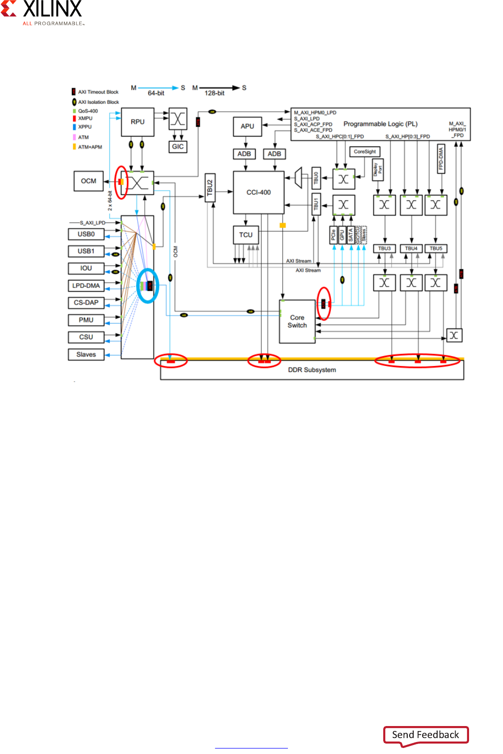
Zynq UltraScale+ MPSoC Embedded Design Methodology Guide 146
UG1228 (v1.0) March 31, 2017 www.xilinx.com
Chapter 7: Resource Isolation and Partitioning
The following figure shows XPPU placement in blue:
The XPPU uses two data structures to control access:
• The Master ID List:
You can program part of this list. The list specifies the masters that are allowed to access
peripherals. Essentially, the list is the pool of potential masters. The first nine masters
are predefined while the remaining 11 are programmable and should be set up before
the XPPU is enabled.
• The Aperture Permission List:
This list defines the set of accessible address apertures and identifies the masters that
can access each aperture. As previously mentioned, the XPPU supports up to 128 x 32B
apertures, 256 x 64 KB apertures, 16 x 1 MB apertures, and 1 x 512 MB aperture (slaves).
A RAM stores the permission settings set up by the software. This RAM is on the system
address map and is accessible just like regular software programmable registers.
X-Ref Target - Figure 7-10
Figure 7-10: XPPU Location in the Zynq UltraScale+ MPSoC Device
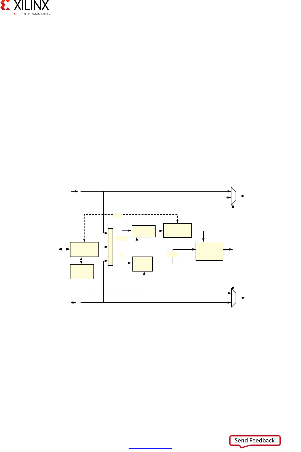
Zynq UltraScale+ MPSoC Embedded Design Methodology Guide 147
UG1228 (v1.0) March 31, 2017 www.xilinx.com
Chapter 7: Resource Isolation and Partitioning
XPPU Operation
The XPPU can be thought of as a 1x1 AXI switch with fine grained access controls. For every
read and write transaction, the XPPU determines if the transaction is allowed. If the
transaction is allowed, it proceeds normally. If the transaction is not allowed, it invalidates
the transaction by poisoning it, much like an XMPU.
For an AXI master to successfully access an AXI slave through the XPPU, the following two
conditions should be met:
• The AXI master's ID must be in the master ID list (for example, the mth entry)
• The AXI slave's entry from the aperture permission list must have a corresponding bit
set in the permission field (that is, PERM[m] == 1).
The above conditions are general rules. Additional checks are added and are detailed
below.
This block-level diagram summarizes the XPPU's operation:
In the previous figure, AXI read transactions arrive near the top of the figure while AXI write
transactions arrive near the bottom. Buried within these transactions are master IDs,
permissions, etc. that are used by the XPPU to determine if the read or write requests are
valid and allowable. The Advanced Peripheral Bus (APB) Interface allows you to program the
XPPU prior to enabling it. The Permission RAM holds permission criteria.
Because the XPPU is a look-up based peripheral protection unit, it uses tables (i.e. master ID
and aperture permission) to determine exactly which master is attempting to read or write
which peripheral. You can find more details about the tables and how they are used in the
Zynq UltraScale+ MPSoC Technical Reference Manual (UG1085) [Ref 7].
X-Ref Target - Figure 7-11
Figure 7-11: XPPU Operation
APB
Interface
AXI
ARADDR
ARID ARADDR
AXI
AWADDR
AWID
AWADDR
APB
Register
File
Permission
RAM
Address
Decode
ADDR
ID
Permission
Check
Match
Data
Aperture
Info
poison
poison
ID
Lookup
X15344-091616

Zynq UltraScale+ MPSoC Embedded Design Methodology Guide 148
UG1228 (v1.0) March 31, 2017 www.xilinx.com
Chapter 7: Resource Isolation and Partitioning
XPPU Permission Checking
Permission checking determines if a read or write transaction is allowed. Basically, the check
is performed by taking the matched master ID lookup and the entry from the aperture
permission list. The incoming AXI master ID (with a mask applied) should be listed in the
master ID list and should also be listed as an allowed master in the aperture permission list.
Furthermore, the incoming secure state should meet the aperture's secure state setting. The
result is further qualified with a parity check on the selected entry from the aperture
permission list if the parity check is enabled.
If all of the above checks pass, then the transaction is allowed. Otherwise, one of the
following errors might have occurred:
• Master ID list parity error
• Master ID list read only error
• Master ID list miss error
• Aperture permission list parity error
• Transaction TrustZone error
• Transaction permission error
You can find more details on XPPU permission checking and how the above errors are
handled in the Zynq UltraScale+ MPSoC Technical Reference Manual (UG1085) [Ref 7].
Transaction Poisoning
As observed in the XPPU functional block diagram presented earlier, if a read or write AXI
transaction does not pass checks, the transaction is poisoned. Poisoning a read transaction
results in all zeros being read, while poisoning a write transaction results in an ignored write
action. The system contains a sink module that takes the poisoned transaction, returns an
error response, and optionally records the lower 12 bits of the transaction address. This can
cause either a data abort or an interrupt to the processor.
XPPU Protection
The XPPU itself is protected in two ways. The master ID list and the aperture permission list
can:
• only be written by secure masters
• be locked from further writes by using the XPPU's own configuration capabilities to
protect the XPPU itself from further writes by setting appropriate entries in the master
ID list and aperture permission list.

Zynq UltraScale+ MPSoC Embedded Design Methodology Guide 149
UG1228 (v1.0) March 31, 2017 www.xilinx.com
Chapter 7: Resource Isolation and Partitioning
Configuration
As in the case of the XMPUs, there are two ways to configure the XPPU:
1. Using the Processor Configuration Wizard (PCW) part of the Vivado Design Suite to
generate the first-stage boot loader (FSBL).
2. At runtime, through a secure AXI master.
Similarly to the XMPU, we recommend you use the PCW to configure the XPPU at boot time
in the FSBL and protect it from further modification to ensure that your system is always
properly configured and secured. Otherwise you have to be very carefully at runtime not to
end up in a situation where resources become unavailable due to erroneous XPPU
configuration.
With regards to the specific regions and rights to use for each region to configure in each
XPPU, this will depend on your design as in the case of the XMPU.
For more information regarding the XPPU, refer to this link in the Zynq UltraScale+ MPSoC
Technical Reference Manual (UG1085) [Ref 7].
Xen Hypervisor
The Xen Hypervisor and its use with the Zynq UltraScale+ MPSoC device were introduced in
Chapter 3, System Software Considerations. Here we will detail a few aspects related to
hypervisors, specifically Xen, with regards to the resource isolation and partitioning
features presented in this chapter.
As outlined earlier, a Hypervisor such as Xen enables you to partition the virtual A53 CPUs
among different guest OSes or between some guest OSes and bare-metal applications.
Referring back to the discussion of TrustZone, note that Xen operates in the non-secure
context and that the ATF operated underneath Xen. Hence all memory accesses initiated by
Xen and the guests it hosts will be issued as non-secure AXI transactions on the AXI
interconnect. The configuration of the XMPU and the XPPU should therefore take into
account the software partitioning you are enforcing with Xen as part of your software
architecture for the APU.
Zynq UltraScale+ MPSoC Embedded Design Methodology Guide 150
UG1228 (v1.0) March 31, 2017 www.xilinx.com
Chapter 8
Security
Security is increasingly at the forefront of any embedded design. The Zynq® UltraScale+™
device provides designers with a comprehensive set of features and capabilities to meet
some of the most demanding modern-day security threats and challenges. This chapter
explains the security philosophy underpinning the Zynq UltraScale+ device's features and
how to use its capabilities to meet your design's security needs.
Defining Your Security Needs
Security is a very vast field and while most practicing designers and engineers recognize its
importance, conducting a thorough security analysis on a projected design requires a fair
level of expertise on the topic. Indeed, the aspects to be addressed are often not limited to
technical vulnerabilities. Instead, your analysis may include such topics such as company
reputation, financial liability, mission-critical safety, and, in some circumstances, matters of
national security.
It would therefore be misleading to provide you with a fixed set of questions to help guide
you through your design's security assessment. Instead, we strongly encourage you to work
with a security expert in your team to understand the threat model surrounding your
design. You should consider the following:
• What is the value of the Intellectual Property you are trying to protect?
• In what environment will the system be deployed? For example, is it unattended and
easily accessible, or is it behind guns, gates and guards?
• Who do you think your adversary is and what are their capabilities?
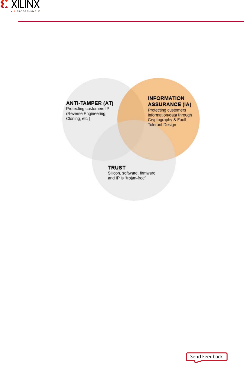
Zynq UltraScale+ MPSoC Embedded Design Methodology Guide 151
UG1228 (v1.0) March 31, 2017 www.xilinx.com
Chapter 8: Security
Security Methodology
As was just mentioned, security is a very broad topic. From the point of view of a system
design based on the Zynq UltraScale+ device, we encourage to look at your design from the
three perspectives illustrated in Figure 8-1.
•Anti-Tamper (AT): AT is sometimes called "physical security". AT protects customers IP
from being reverse engineered, cloned, stolen, modified, or otherwise used in a fashion
that does not conform to your system's design goals. If you place value on your own IP,
then AT is important to your security strategy.
•Information Assurance (IA): Protects information and data being processed through
industry standard cryptography and fault tolerant design methodologies.
•Trust (Supply Chain Security): Ensures the silicon, software, firmware, and IP is
"trojan-free".
As you can see from Figure 8-1, all three disciplines overlap and intersect each other, hence
the need to analyze security in a holistic fashion. In addition to involving several disciplines,
security is also a multi-layered affair. While you might at first feel that you are most
interested in specific aspects, Figure 8-2 illustrates how security layers are built on top of
each other.
X-Ref Target - Figure 8-1
Figure 8-1: Basic Security Disciplines
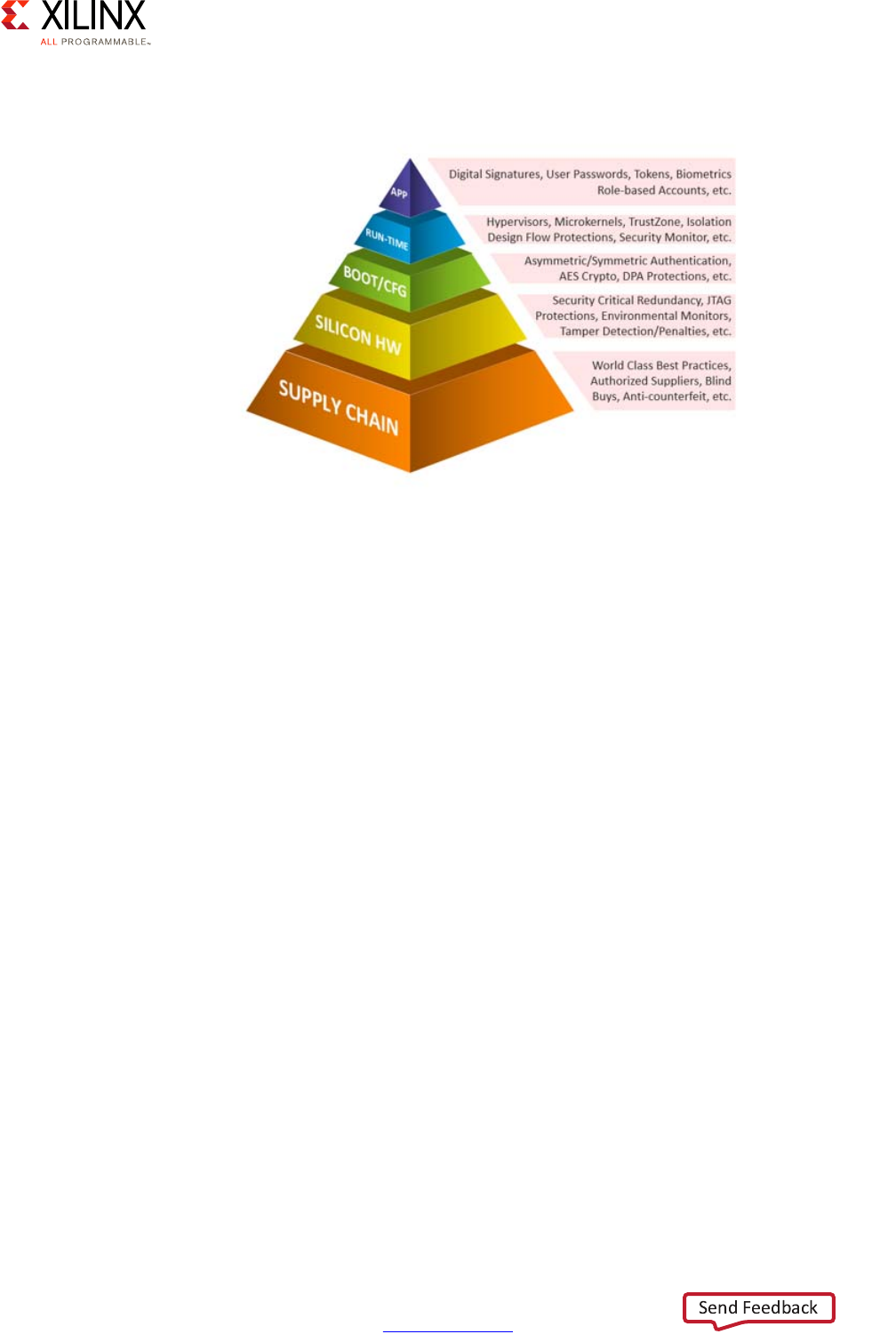
Zynq UltraScale+ MPSoC Embedded Design Methodology Guide 152
UG1228 (v1.0) March 31, 2017 www.xilinx.com
Chapter 8: Security
As you can see, trust in the supply chain, such as making sure you are using best practices
and authoritative suppliers, is the cornerstone of your security architecture. This base
ensures devices do nothing except what they are intended to do. This is taken care of by
Xilinx.
Moving up the pyramid, security features are in place to protect the silicon itself from
attacks such as physical tampering, by way of varying and/or measuring temperature,
voltage or otherwise, or abuse of legitimate device functionality like JTAG. This is also taken
care of by Xilinx.
Moving further up, the boot and configuration processes are protected through the
application of information assurance tenets: Confidentiality, Authentication, and
Integrity.Xilinx provides designers with the capabilities to do this, but it is up to you to use
them properly.
Even further up are software levels higher in the stack such as Hypervisor protections,
TrustZone, and monitors. Again, Xilinx provides capabilities that must be used
appropriately.
Finally, signatures, passwords established by the user can protect applications at the very
top. At this level, the responsibility is mainly with system designers to do things correctly.
Effectively, security has a life cycle that goes from the supply chain to the device that is
running in the field.
X-Ref Target - Figure 8-2
Figure 8-2: Security Pyramid
Zynq UltraScale+ MPSoC Embedded Design Methodology Guide 153
UG1228 (v1.0) March 31, 2017 www.xilinx.com
Chapter 8: Security
Organizations and forums exist that can keep you abreast of security efforts across the
industry. Xilinx holds its own annual Xilinx Security Working Group (XSWG) event in North
America and Europe that brings together Xilinx aerospace, defense and commercial
customers, academic representatives, Xilinx Alliance Members and government agencies to
discuss the latest security topics. These topics include supply chain protections, device
security, secure boot, and runtime security.
Note that whereas this chapter's title explicitly mentions "security", various topics related to
security are discussed in other chapters as well:
•Chapter 2, Processing System introduces the interconnect through which the majority
of cross-component communication occurs within the Zynq UltraScale+ device.
•Chapter 7, Resource Isolation and Partitioning discusses various runtime
security-related mechanisms such as TrustZone, the Xilinx® Memory Protection Unit
(XMPU) and the Xilinx Peripheral Protection Unit (XPPU).
•Chapter 5, Programmable Logic covers the Isolation Design Flow (IDF), a fault-tolerant
design methodology, to be used to segregate IP functionality found in the
programmable logic (PL).
Security Features Overview
As security is a constant "arms race", Xilinx works hard to stay ahead of threats by
continuously adding security features and features, and enhancing existing ones. Figure 8-3
summarizes the built-in security features across the Xilinx product lines with the two
right-most columns listing UltraScale+ features.
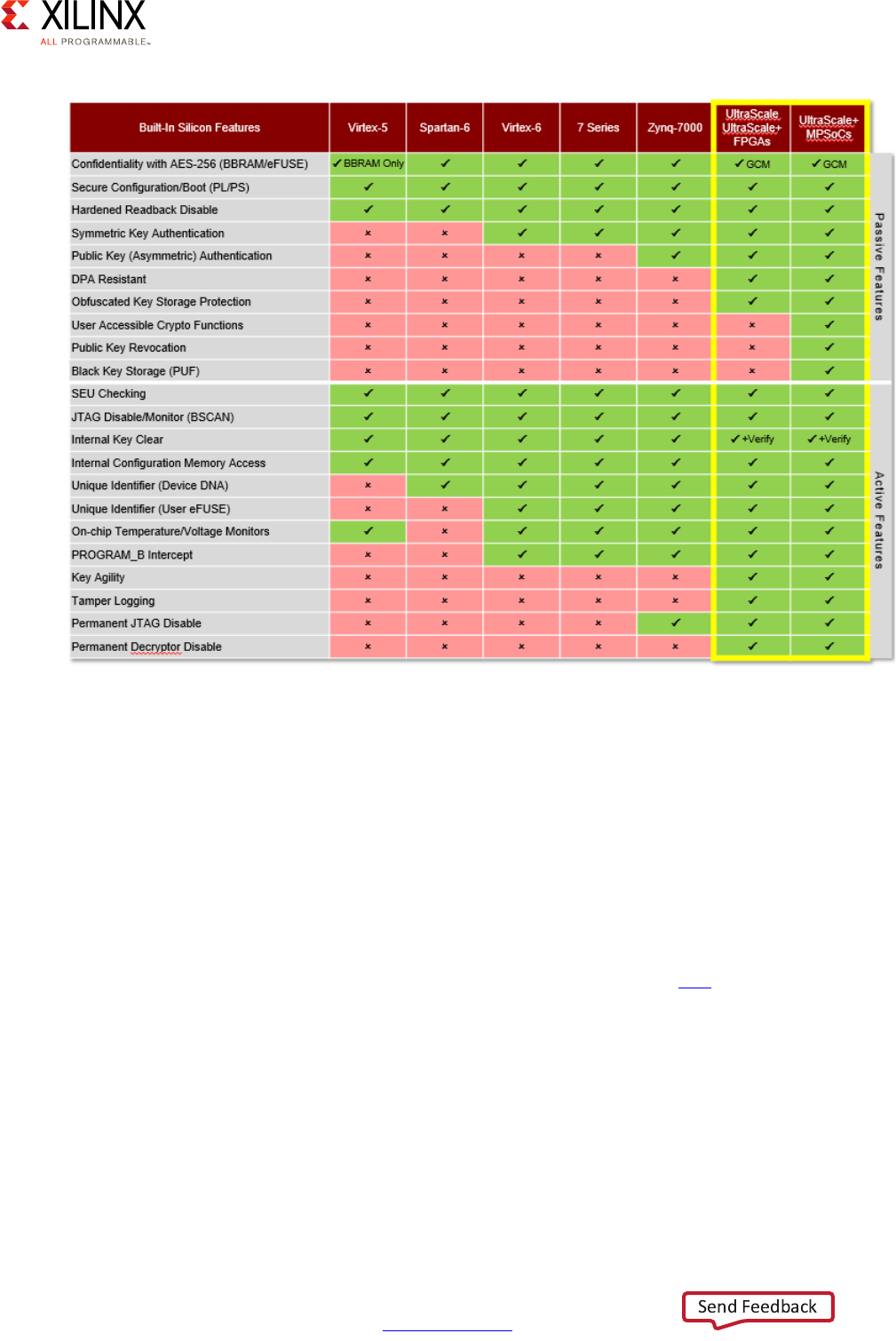
Zynq UltraScale+ MPSoC Embedded Design Methodology Guide 154
UG1228 (v1.0) March 31, 2017 www.xilinx.com
Chapter 8: Security
Security features are categorized into two groups: passive features and active features.
Passive security features are built into the device and do not require the designer to do
anything extra in their design. For example, secure configuration/boot and authentication
fall into this group. Active security features require the designer to deliberately activate
some of the Zynq UltraScale+ device's capabilities at design or at run time. An example of
an active security feature is when the device has been configured to monitor a specific
voltage and temperature operating range.
Understanding the Zynq UltraScale+ device's features and knowing what types of attacks
for which they are in place will help you decide which features are right for your
implementation. You can find more information on security at this link in the Zynq
UltraScale+ MPSoC Technical Reference Manual (UG1085) [Ref 7].
X-Ref Target - Figure 8-3
Figure 8-3: Xilinx Security Features
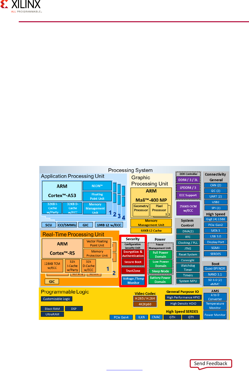
Zynq UltraScale+ MPSoC Embedded Design Methodology Guide 155
UG1228 (v1.0) March 31, 2017 www.xilinx.com
Chapter 8: Security
Configuration Security and Secure Boot
With the chain of trust secured from the manufacturer to the customer, one the first
priorities for system designers to understand is the securing of an SoC's boot process.
Indeed, it's crucial for on-chip logic and firmware to ensure that the chain of software
loaded at startup is properly signed with authorized keys found on the device at boot time,
ensuring what is commonly known as hardware root of trust. Alternatively, it's possible to
boot unsigned images, but if that's the best avenue for your system's design then security
is probably not an issue to begin with in your case. During early development, it can be
customary to operate with unsigned images, say by loading them through JTAG.
In the case of the Zynq UltraScale+ device, secure boot is facilitated by the Platform
Management Unit (PMU) and the Configuration Security Unit (CSU). In addition to being
part of the boot process, the CSU is also responsible for many other security-related
functions in the Zynq UltraScale+ device, as we will see shortly. The CSU ensures hardware
root of trust by enabling the use of RSA for Asymmetric Authentication followed by
AES-GCM for confidentiality (encryption/decryption). The following figure shows the CSUs
in the overall system block diagram for the Zynq UltraScale+ MPSoC device.
X-Ref Target - Figure 8-4
Figure 8-4: Configuration Security Unit
Zynq UltraScale+ MPSoC Embedded Design Methodology Guide 156
UG1228 (v1.0) March 31, 2017 www.xilinx.com
Chapter 8: Security
Figure 8-5 shows the responsibilities of the PMU and CSU at boot time.
Boot flow consists of three stages:
•Pre-Configuration: Once it is determined that the system needs to boot ("power-on
reset" or POR), the PMU executes the PMU ROM setup. The PMU handles all reset and
wake-up processes.
•Configuration: The CSU takes over and ensures that the FSBL gets loaded into the
on-chip memory (OCM). During configuration, the FSBL image is authenticated (if the
hardware root of trust is enabled), and decrypted, and loaded into the OCM for either
the application processing unit (APU) or real-time processing unit (RPU) to use.
•Post-Configuration: Once the FSBL begins to execute, the CSU goes into a monitoring,
tamper-resistant state.
As explained in the System Software Considerations Chapter, the Zynq UltraScale+ device
supports booting from Quad-SPI, NAND, SD, and eMMC external devices. Using such
storage devices, the CSU is able to guarantee hardware root of trust. Secondary boot is
available from SATA, Ethernet and PCIe. It is also possible using a minimal FSBL, but the
responsibility to ensure secure booting from such devices is left to the system designer.
When the boot ROM executes, it looks for a valid image to load. A valid image is determined
through an image identification string. These techniques allow for an external device to
X-Ref Target - Figure 8-5
Figure 8-5: High Level Boot Flow
Test I/F Lockdown
Zeroize PMU Registers
Run LBIST*
SHA3/384 Integrity
Check of PMU ROM
Release Reset to PMU
Zeroize Registers
LPD/FPD*
Zeroize PMU RAM
Voltage Checks
(LPD, AUX, I/O)
Zeroize memories on CSU,
LPD and FPD
SHA3/384 Integrity Check
of CSU ROM
Release Reset to CSU
Enforces HW Root of Trust when enabled
Enforces Security “State”
Validate Integrity of User Public Key
Public Key Revocation
FSBL and PMU FW*
Authentication/Decryption*
Zeroize storage elements after processing
(including fallback)
Release Reset to RPU/APU
HW PMU CSU
CSU Tamper Monitoring
Load FSBL and
PMU FW1
PMU Release
CSU
HW Release
PMU
Power
Valid
NOTE:
1. Authentication with optional decryption.
Power Monitoring
X18922-032917
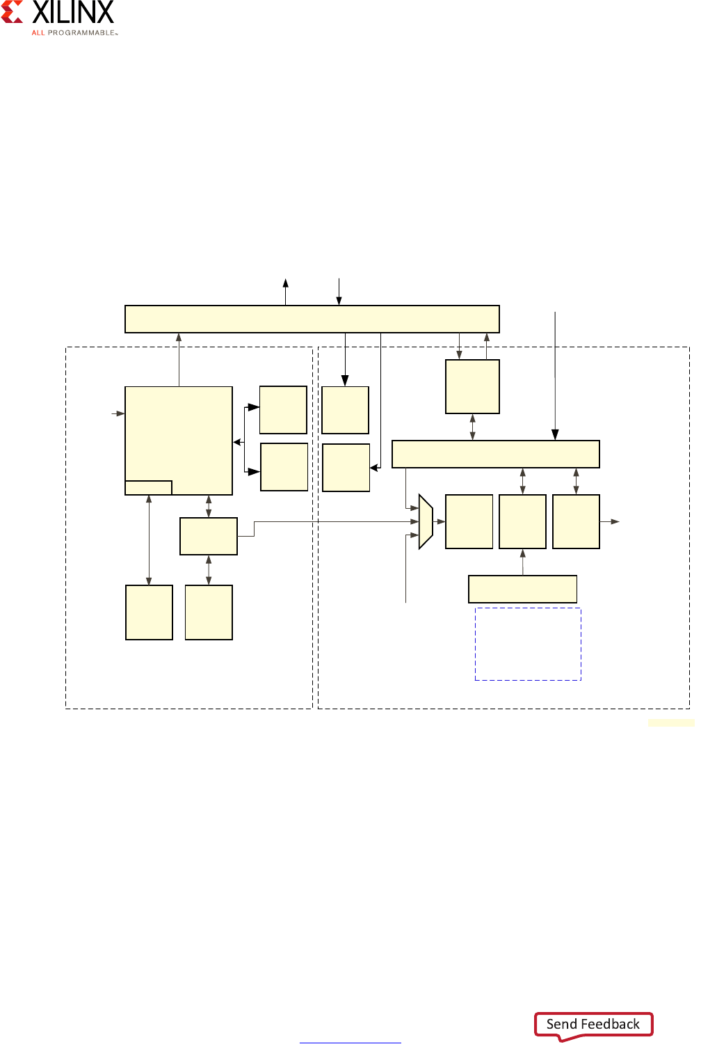
Zynq UltraScale+ MPSoC Embedded Design Methodology Guide 157
UG1228 (v1.0) March 31, 2017 www.xilinx.com
Chapter 8: Security
contain more than a single boot image for use across the various processing devices on the
Zynq UltraScale+ device. This scheme also allows for fallback and multiboot image search
to be used.
A boot image to be checked and booted is loaded from an external boot device to the Zynq
UltraScale+ device through use of the CSU block and its triple-redundant MicroBlaze™
processor, security blocks, CSU DMA, Secure Stream Switch (SSS) and Processor
Configuration Access Port (PCAP). Figure 8-6 shows the CSU Block and the various pieces
that facilitate secure boot.
On the left is the triple-redundant MicroBlaze processor along with the CSU RAM and ROM.
This includes the Physically Unclonable Function (PUF) block, which provides a way to
generate a device-unique encryption key. On the right are the blocks that manage
encryption and decryption keys, the various decryption processes (AES-GCM and RSA),
known as the Crypto-Interface Block (CIB). Also, the CSU DMA process block through which
the SSS functions.
One important aspect of the CSU's role is key management. As can be seen in the following
table, the CSU can use one of several keys for its AES-GCM functionality.
X-Ref Target - Figure 8-6
Figure 8-6: Configuration Security Unit (CSU) Block Diagram
CSU PMU Switch
ROM
Validation
ROM
(128 KB)
RAM
(32 KB)
Triple
Redundant
MicroBlaze
SHA-3
384
AES-
GCM
256
Secure Stream Switch
PCAP
CSU DMA
CSU
Registers
Key
Management
To PL
Configuration
PMU ROM
Validation
To/From LPD Main Switch
Tamper
Sources INTC
ECC
BBRAM
eFUSE
PUF
Operation
KUP
Family
CSU
Local
Registers
PUF RSA
Multiplier
PSTP
Security Processor Block Crypto Interface Block
X15318-032917
Zynq UltraScale+ MPSoC Embedded Design Methodology Guide 158
UG1228 (v1.0) March 31, 2017 www.xilinx.com
Chapter 8: Security
With regards to BBRAM an eFUSE, note that the keys programmed onto the Zynq
UltraScale+ device cannot be retrieved in any fashion. Only a CRC is available for checking
whether the key was programmed correctly.
Once the CSU is done and the FSBL is executing, the CSU monitors the system for a tamper
response and, should tampering be detected, can execute a number of user-defined
responses, including secure lockdown.
The details of the software components that the designer can select and configure at boot
time are covered in the System Software Considerations chapter. That is, the process from
the booting of the FSBL and onwards.
Note that it is the responsibility of the FSBL responsibility to load the bitstream for the PL
through the CSU's PCAP using the CSU DMA. This process is automated when using the
Vivado® Design Suite.
See the following references for more information:
• For more information about the CSU, refer to this link in the Zynq UltraScale+ MPSoC
Technical Reference Manual (UG1085) [Ref 7].
Table 8-1: Types of Keys
Key Name Description
BBRAM The battery backed RAM (BBRAM) key is stored in plain text form in a 256-bit
SRAM array. To extend battery life, the SRAM array receives its power from
VCCAUX when VCCAUX is powered. Otherwise the SRAM array is powered
by VCCBAT.
Boot The boot key register holds the decrypted key while the key is in use.
eFUSE The eFUSE key is stored in eFUSEs. It can be either plain text, obfuscated (i.e.,
encrypted with the family key), or encrypted with the PUF KEK.
Family The family key is a constant AES key value hard-coded into the devices. The
same key is used across all devices in the Zynq UltraScale+ MPSoC family.
This key is only used by the CSU ROM to decrypt an obfuscated key. The
decrypted obfuscated key is used to decrypt the boot images. The
obfuscated key can be stored in either eFUSE or the authenticated boot
header. Because the family key is the same across all devices, the term
obfuscated is used rather than encrypted to reflect the relative strength of
the security mechanism.
Operational The operational key is obtained by decrypting the secure header using a
plain text key obtained from the other device key sources. For secure boot,
this key is optional. The operational key is specified in the boot header and
minimizes the use of the device key, thus limiting its exposure.
PUF KEK The PUF KEK is a key-encryption key that is generated by the PUF.
Key update register User provided key source. After boot, a user selected key can be used with
the hardened AES accelerator.
Zynq UltraScale+ MPSoC Embedded Design Methodology Guide 159
UG1228 (v1.0) March 31, 2017 www.xilinx.com
Chapter 8: Security
• For more information about the programming of the PL bitstream through the CSU's
PCAP, refer to this link in the Zynq UltraScale+ MPSoC Technical Reference Manual
(UG1085) [Ref 7].
• Several aspects related to boot time security are covered at this link in the Zynq
UltraScale+ MPSoC: Software Developers Guide (UG1137) [Ref 5].
Device and Data Security
Whereas the CSU and secure boot ensure that the device starts securely, the Zynq
UltraScale+ MPSoC device also includes capabilities and features to ensure runtime security
of the device.
Tamper Monitoring and Response
As mentioned in Security Methodology, page 151, anti-tamper (AT) helps protect your IP
from being reverse engineered, cloned, and otherwise manipulated in an unauthorized
fashion. Also as mentioned in the previous section, the CSU's primary function after the
FSBL begins execution is to run in a monitoring mode that looks for tampering events.
Tamper events can, for instance, be detected through voltage and temperature monitoring
of the Zynq UltraScale+ device.
You can control tamper response by setting CSU tamper registers as shown in the following
table.
Table 8-2: Tamper and Monitor Registers
Register Monitor Description
csu_tamper_12 AMS voltage alarm for GT.
csu_tamper_11 AMS voltage alarm for PSIO bank 3.
csu_tamper_10 AMS voltage alarm for PSIO bank 0/1/2.
csu_tamper_9 AMS voltage alarm for DDRPHY.
csu_tamper_8 AMS voltage alarm for VCCPAUX.
csu_tamper_7 AMS voltage alarm for VCCPINT_FPD.
csu_tamper_6 AMS voltage alarm for VCCPINT_LPD.
csu_tamper_5 AMS over and under temperature alarm for APU.
csu_tamper_4 AMS over and under temperature alarm for LPD.
csu_tamper_3 PL SEU error.
csu_tamper_2 JTAG toggle detect.
csu_tamper_1 External MIO.
csu_tamper_0 CSU register.
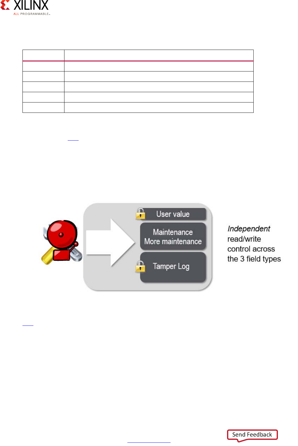
Zynq UltraScale+ MPSoC Embedded Design Methodology Guide 160
UG1228 (v1.0) March 31, 2017 www.xilinx.com
Chapter 8: Security
The responses possible to these tamper events are shown in the following table.
Under some circumstances, you might also want to impose severe and permanent penalties
upon detection of a tamper event. Refer to the“Revocation as a Tamper Penalty” section,
located at this link in the Zynq UltraScale+ MPSoC Technical Reference Manual (UG1085)
[Ref 7] for such an example.
The Zynq UltraScale+ device also provides a number of user-definable eFUSE bits that can
be used for creating unique identifiers or for logging data about maintenance or tamper
events for post-mortem forensic analysis, as illustrated in Figure 8-7.
For more information about using eFUSEs to get unique IDs for data logging, refer to this
link in the Zynq UltraScale+ MPSoC Technical Reference Manual (UG1085) [Ref 7].
System Monitor
In addition to the CSU's capabilities, the Zynq UltraScale+ device also includes system
monitor (SYSMON) blocks both the PS and in the PL. The SYSMON is for use for custom
and/or advanced environment monitoring. It is self-contained and delivered pre-verified
and pre-implemented, integrates Xilinx security features and provides extreme ease of use.
Table 8-3: Tamper Monitor and Response Bits
Bit Response
4 Erase the BBRAM key in addition to taking any below option.
3 Secure lockdown and 3-state all I/O.
2Secure lockdown.
1 System reset.
0 System interrupt.
X-Ref Target - Figure 8-7
Figure 8-7: Tamper and Maintenance Logging
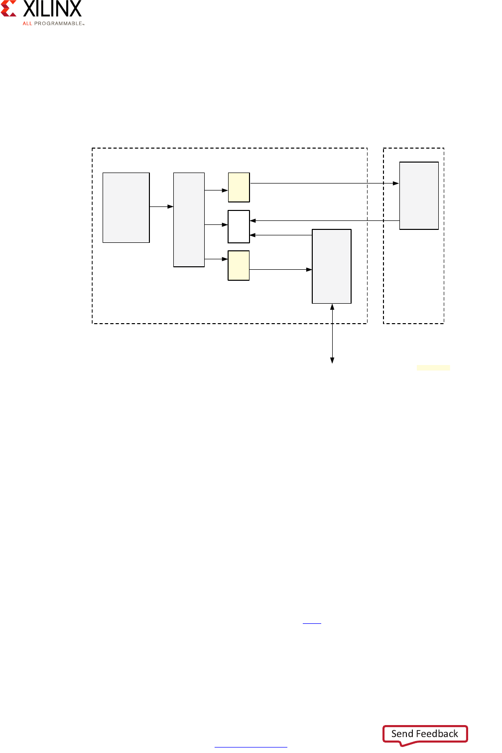
Zynq UltraScale+ MPSoC Embedded Design Methodology Guide 161
UG1228 (v1.0) March 31, 2017 www.xilinx.com
Chapter 8: Security
You can, for instance, use the SYSMON block register interface to configure the block and
provide the capability to monitor on-chip voltages as well as junction temperature. The
SYSMON block also has built-in alarm generation logic that is used to interrupt the
processor based on certain alarm conditions. For example, it can shut the system down
based on an over-temperature (OT) alarm generation. Figure 8-8 illustrates the SYSMON
blocks found in the Zynq UltraScale+ device.
The SYSMON has the following security and safety features:
• JTAG port monitoring and blocking
• Power supply voltage monitoring including Low Power Domain (LPD)
• Device die temperature monitoring (APU, RPU, and PL)
• User clock monitoring (eight frequency monitors) and watchdog
• Partial configuration management
• Configuration RAM integrity monitoring
• Built-In Self Test, which is used to check itself
You can configure the SYSMON through the Dynamic Reconfiguration Port (DRP), which is
accessible through the LPD I/O Peripheral Address Map.
For complete information on the SYSMON, see this link in the Zynq UltraScale+ MPSoC
Technical Reference Manual (UG1085) [Ref 7].
X-Ref Target - Figure 8-8
Figure 8-8: System Monitor Block
AXI/APB
Interconnect APB
Splitter
Registers
APB
To
DRP
PS
SYSMON
PL
SYSMON
DRP Bus
Alarm
Alarm
DRP Bus
Remote Temperature Sensor
from Full Power Domain
PS Lower Power Domain PL
APB
To
DRP
X15149-021216

Zynq UltraScale+ MPSoC Embedded Design Methodology Guide 162
UG1228 (v1.0) March 31, 2017 www.xilinx.com
Chapter 8: Security
Protection Against DPA Attacks
Differential Power Analysis (DPA) attacks involve using statistics and signal sampling of
power usage, or other emanations, across a device as it decrypts information over periods
of time and analyzing changes to gain knowledge of the secret key. These types of attacks
are known as "side-channel attacks", an attempt to derive information about the device or
what it's doing by monitoring system implementation instead of using brute force or trying
to find weaknesses in the cryptographic algorithms used.
To help against DPA attacks, you can use balanced circuits to minimize measurable swings
in power or emission, or you can add noise to raise the noise floor for measurements. The
approach used by the Zynq UltraScale+ device with regards to image loading is to limit the
amount of data an adversary can collect, thus preventing the adversary from performing
the needed analysis on the side channel information.
DPA attacks generally come in two forms:
•Random Data Attack: This attack is when an adversary pumps random data into the
cryptographic system in order to collect enough side channel information to extract
the "secret", which is they AES key.
•Good Data Attack: Because programming files are quite large, an adversary might be
able to use a valid image as input to the cryptographic system and collect enough side
channel information in order to perform their analysis.
To protect against a random data attack, public key asymmetric authentication (RSA) is
performed before decryption. By doing this, only authorized images are allowed to be
decrypted.
To protect against a good data attack, you have the option of breaking up boot images into
smaller blocks, each encrypted with its own key (key rolling). You can choose the size of the
block and only the first key needs to be stored in the device (eFUSE or BBRAM). All
subsequent keys are protected, authenticated, and decrypted, in the previous blocks.
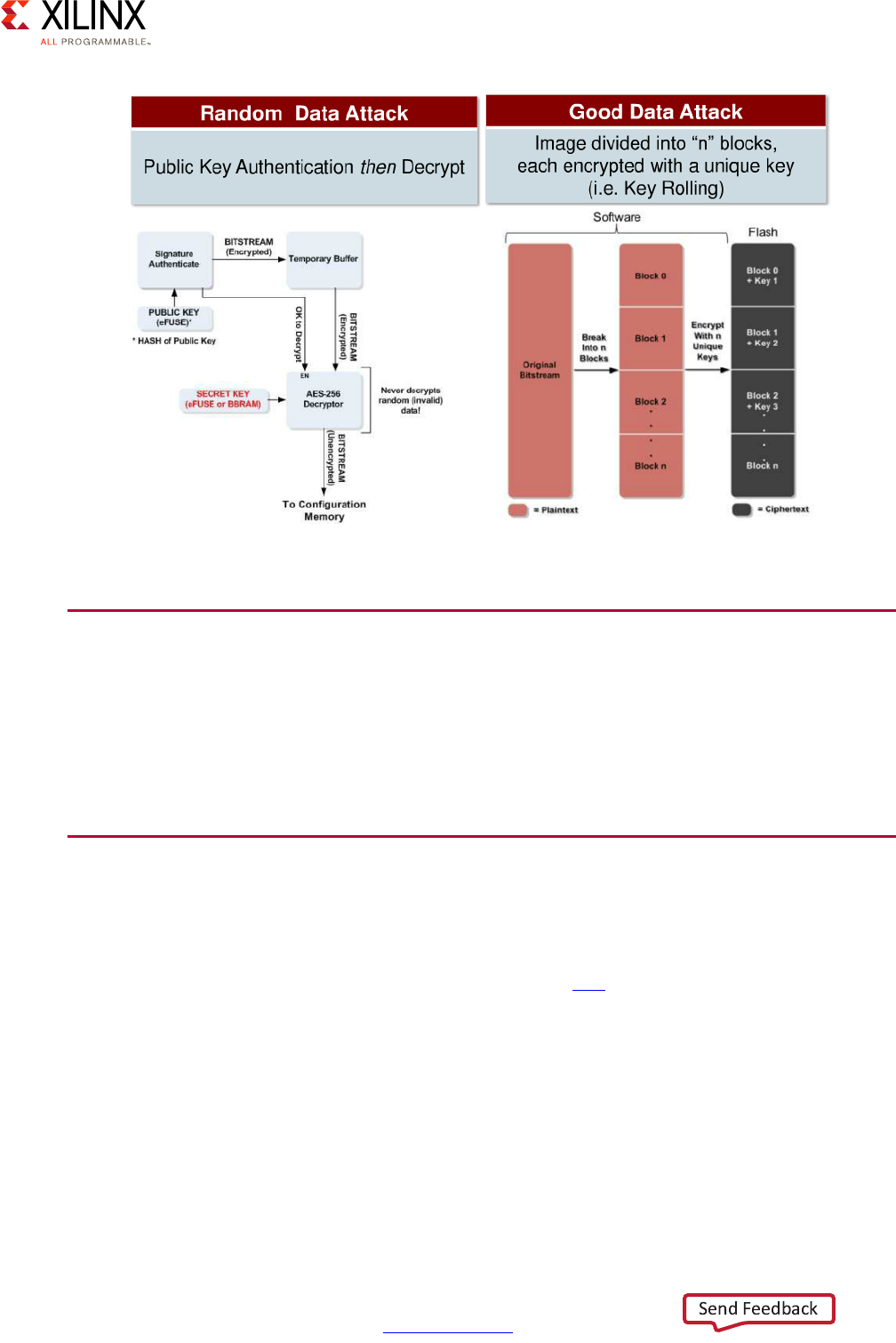
Zynq UltraScale+ MPSoC Embedded Design Methodology Guide 163
UG1228 (v1.0) March 31, 2017 www.xilinx.com
Chapter 8: Security
CSU Hardware Accelerators
In addition to being useful at boot time, the CSU's cryptographic capabilities can be used
for hardware acceleration of cryptographic functions, namely for RSA, SHA, and AES-GCM.
Refer to Zynq UltraScale+ MPSoC Technical Reference Manual (UG1085) [Ref 7] for further
details on these capabilities.
Functional Safety
Another aspect closely related to security is functional safety, which is a discipline
concerned with system operation correctness. The Zynq UltraScale+ device contains several
features supporting functional safety as covered at this link in the Zynq UltraScale+ MPSoC
Technical Reference Manual (UG1085) [Ref 7].
The lockstep mode of the RPU, for instance, is ideal for safety critical applications. That is
especially true if as part of the design process a subset of your application may have to
meet functional safety standards like IEC61508 and/or ISO26262. The ARM Cortex R5s in the
RPU have been architected towards applications that require high reliability and responding
to hardware system faults. Also, the Xilinx design tool suite addresses Functional Safety
Design flows with a set of tools that meet TUV SUD certification, helping to speed the safety
certification process for your project.
X-Ref Target - Figure 8-9
Figure 8-9: Differential Power Attack (DPA) Countermeasures

Zynq UltraScale+ MPSoC Embedded Design Methodology Guide 164
UG1228 (v1.0) March 31, 2017 www.xilinx.com
Chapter 8: Security
Reliability and FIT identification and response in the processing system is accomplished
through the isolation architecture of the Zynq UltraScale+ device. The RPU can be isolated
as a completely separate system from the rest of the Zynq UltraScale+ device architecture
with access defined to a limited set of peripherals and memory locations. At the
interconnect level access is enforced through the use of the Xilinx Memory Protection Unit
(XMPU) and Xilinx Peripheral Protection Unit (XPPU) covered in the Resource Isolation and
Partitioning Chapter, these components ensure that data transactions on either memory or
peripherals is limited to only authorized subsystem components. In addition the ARM
TrustZone architecture checks each data transaction for authorized access to the correct
subsystem.
For more information on how functional safety concerns can be addressed regarding your
design see, the Xilinx All Programmable Functional Safety Design Flow Solution Product Brief
(PB015) [Ref 12] and the Xilinx Reduces Risk and Increases Efficiency for IEC61508 and
ISO26262 Certified Safety Applications White Paper (WP461) [Ref 13].

Zynq UltraScale+ MPSoC Embedded Design Methodology Guide 165
UG1228 (v1.0) March 31, 2017 www.xilinx.com
Chapter 9
Multimedia
The Zynq® UltraScale+™ MPSoC device combines state of the art Programmable Logic with
a DisplayPort that includes video and audio processing capabilities, a graphics processing
unit (GPU) geared for low-power consumption and a video codec unit (VCU) for
simultaneous video encoding and decoding. This rich set of multimedia capabilities
provides you with the power and flexibility required to tackle some of the most demanding
multimedia applications. This chapter covers these capabilities along with the
recommendations for their use.
Defining Your Multimedia Needs
Multimedia applications are typically very demanding of system resources and while the
Zynq UltraScale+ MPSoC device is tailored for multimedia, you must still have a good
understanding of how your multimedia needs fit with the Zynq UltraScale+ MPSoC device's
capabilities. Namely, you must identify data processing paths and understand their
interactions in light of the system interconnect and memory functionality, as discussed in
the Processing System and Memory chapters.
To assist you in this task, we encourage you to begin by answering the following questions:
• Does your design need accelerated graphics?
• Are you using the Zynq UltraScale+ MPSoC device as part of a system that has a user
display?
• Does your application have audio output?
• What OS do you plan on using on the application processing unit (APU)?
• Does your design have custom multimedia processing needs?
Zynq UltraScale+ MPSoC Embedded Design Methodology Guide 166
UG1228 (v1.0) March 31, 2017 www.xilinx.com
Chapter 9: Multimedia
Multimedia Methodology
As in previous chapters, the approach we take here to discuss the Zynq UltraScale+ MPSoC
device's multimedia capabilities is to focus on the system components most relevant to that
topic. As such, Figure 9-1 illustrates the key Zynq UltraScale+ MPSoC device blocks
involved in multimedia and their typical interaction. One key component not illustrated is
the APU which will almost always be invariably involved as soon as a multimedia software
stack is necessary. The APU, however, is mostly acting as a command-and-control
component and is not involved in the bulk of the data transfers or operations required for
multimedia processing, which are the important factors to keep in mind during multimedia
design.
Note: Figure 9-1 does NOT attempt to precisely represent the Zynq UltraScale+ MPSoC device's
internal blocks. Instead, it's primarily a conceptual view for the purposes of the present explanation.
Per Figure 9-1, the most important component to keep in mind with regards to multimedia
is memory. Multimedia operations are typically memory transfer intensive. Hence, anything
that can be done to minimize memory transfers will benefit multimedia throughput. In the
cases where the transfers can't be avoided then a solid understanding of the paths involved,
including which other parties need to use them concurrently, will be required to ensure
proper system function.
The GPU, for instance, mainly takes the data to be rendered from the RAM and returns the
rendered content to the display buffers also found in RAM. The DisplayPort, reads the video
X-Ref Target - Figure 9-1
Figure 9-1: Zynq UltraScale+ MPSoC Device Multimedia Components
GPU
VCU
Programmable Logic
PS-GTR
DisplayPort
Displa
y
Port
DDR
Memory
Controller
X18927-032117
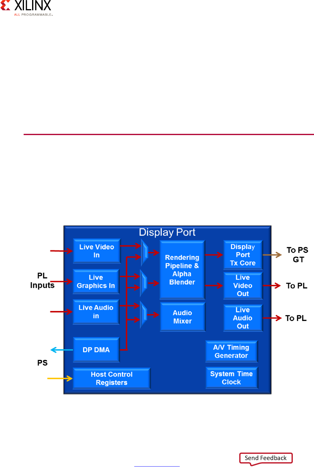
Zynq UltraScale+ MPSoC Embedded Design Methodology Guide 167
UG1228 (v1.0) March 31, 2017 www.xilinx.com
Chapter 9: Multimedia
and audio buffers from memory and sends its output to the PS-GTR transceiver? or feeds it
for further processing to the programmable logic (PL). Finally, the encoding and decoding
operations of the VCU also depend on data coming from and going to memory. Hence,
make sure you have a solid understanding of the interconnect as explained in Chapter 2,
Processing System and refer back to Chapter 6, Memory for recommendations on dealing
with cases where existing memory bandwidth is insufficient for your application.
Another crucial aspect with regards to multimedia is software support. Xilinx provides
Linux-based software stacks for the Zynq UltraScale+ MPSoC device's multimedia
capabilities. Hence, you will need to run Linux on the APU if you want to benefit from those
stacks.
DisplayPort
The Zynq UltraScale+ MPSoC device's DisplayPort controller conforms to the VESA
DisplayPort v1.2a source-only specification and provides support for video, graphics and
audio. Its video and graphics pipelines function independently up to the alpha blending or
chroma keying stages where they are mixed. Figure 9-2 provides a simplified view of the
DisplayPort controller's data flow.
X-Ref Target - Figure 9-2
Figure 9-2: Simplified DisplayPort Block Diagram
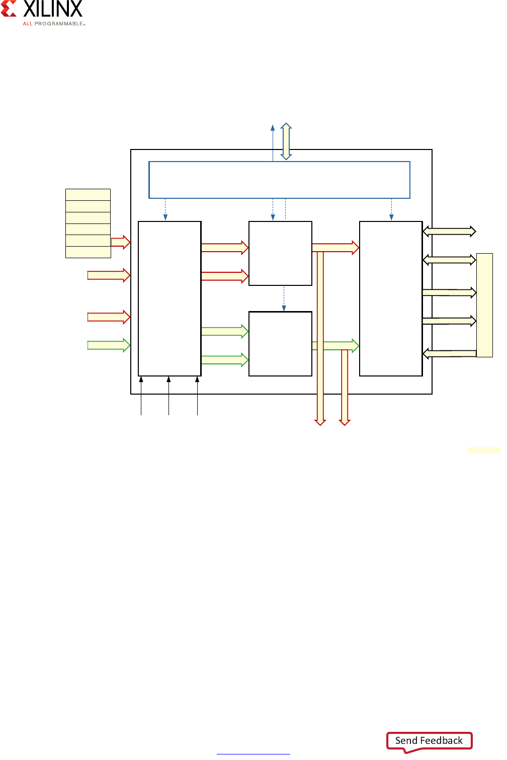
Zynq UltraScale+ MPSoC Embedded Design Methodology Guide 168
UG1228 (v1.0) March 31, 2017 www.xilinx.com
Chapter 9: Multimedia
Effectively, the DisplayPort has two sources of data. It can act as a DMA master and retrieve
non-live data from memory, and it can receive live data from the PL. Its output can either go
to the PS-GTR or to the PL. Figure 9-3 provides a more detailed view of the DisplayPort's
functionality.
Video/Graphics Rendering Pipeline
The video rendering pipeline seen as part of the DisplayPort controller in the previous
section can have several input streams that must be coalesced into a single video output. As
we just saw, there are two main sources of input to the DisplayPort: live data from the PL
and in-memory buffers. The former is linked into the DisplayPort directly from the PL
whereas the latter is transferred using direct memory access (DMA). Figure 9-4 illustrates
the video rendering pipeline's processing of its various input streams.
X-Ref Target - Figure 9-3
Figure 9-3: Data Flow in the DisplayPort Controller
Interrupt
High Level Address Decoder
APB
Display Port
Source
Controller
Link layer and PHY layer
logic. PS-GTR is at
the system level.
128-bit AXI-S (Memory)
Live Native Video Input
(36-bit Video +
36-bit Graphics +
8-bit Alpha)
Live Audio Input
(AXI-S 32-bit)
Video Stream 1
AUX + HPD
Native Video
(Mapped to
48-bit)
APB Master
Lane0: 16-bit
Data + 2-bit
Lane1: 16-bit
Data + 2-bit
PS-GTR Status
32-bit AXI-S
(Audio)
Video Stream 2
Audio Stream 1
Audio Stream 2
Blended
Video to
PL
Mixed
Audio to
PL
External
VSYNC
Event
External
Custom
Event 1
External
Custom
Event 2
Audio/Video Buffer
Manager
and
STC
Audio Mixer
Video Rendering
Pipeline
Channel 0
Channel 1
Channel 2
Channel 3
Channel 4
Channel 5
DPDMA
PS-GTR
X16959-092516
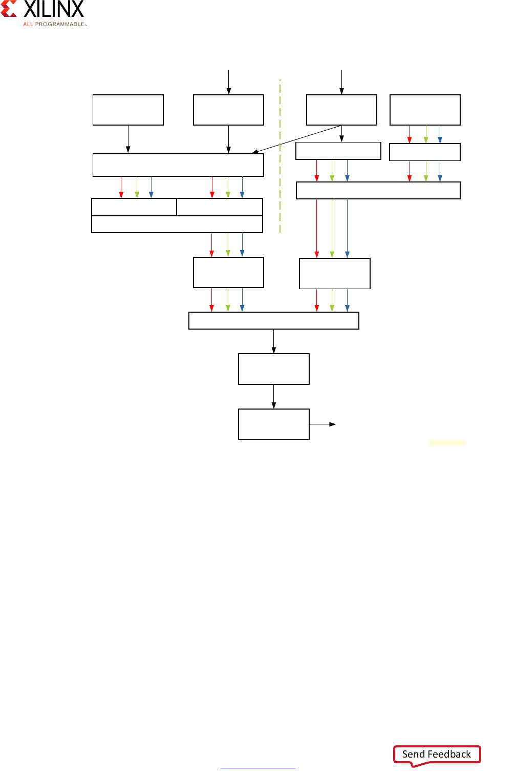
Zynq UltraScale+ MPSoC Embedded Design Methodology Guide 169
UG1228 (v1.0) March 31, 2017 www.xilinx.com
Chapter 9: Multimedia
The video pipeline can be set to operate in the following modes:
• Live Presentation Mode:
°In this mode, the PL is the only A/V data source. The timing information from the
A/V data is used to drive the DisplayPort controller.
• Non-Live Presentation Mode:
°In this mode, the A/V data is fetched from memory though AXI using the
DisplayPort DMA. In this mode, software assistance is required to properly
synchronize audio and video. This is done by providing timestamps inside the DMA
descriptor used by the DisplayPort controller. The features of the DisplayPort DMA
(DPDMA) are presented below.
• Mixed Presentation Mode:
°This mode is a mix between the two previous operating modes.
X-Ref Target - Figure 9-4
Figure 9-4: DisplayPort Controller Video Rendering Pipeline Block Diagram
Test Pattern
Generator
Live Video
Interface DisplayPort DMA Live Graphics
Interface
MUX Split
4:2:0 or 4:2:2
CHROMA Up Sampling
Color Space
Conversion
Color Space
Conversion
Alpha Blending
Color Space
Conversion
Chroma
Sub-sampling
MUX
Pallete or Bypass
Video Rendering Pipeline
Video Graphics
To Display Port Core/PL
4:2:2 or 4:4:4
4:2:2 or 4:4:4
X15506-092516
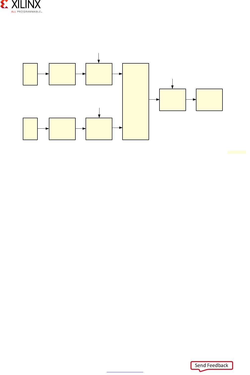
Zynq UltraScale+ MPSoC Embedded Design Methodology Guide 170
UG1228 (v1.0) March 31, 2017 www.xilinx.com
Chapter 9: Multimedia
The blending stage can be done in two ways as illustrated in Figure 9-5, alpha blending or
chroma keying.
Alpha Blending
Alpha blending is the default technique by which the two data sources are mixed by the
DisplayPort controller. Alpha blending is a predefined mathematical process to blend two
images together. Several parameters of the alpha blending process (blending matrix,
coefficient, etc.) can be programmed through registers in the DisplayPort controller.
Chroma Keying
Chroma keying is a video technique for layering two images or video streams. This is the
technical name for the technique commonly known as "green screen" in cinematography.
This stage of the video pipeline demands the selection of a single key color. At the exit of
the pipeline stage, the key color will have been replaced by the content of the second data
source of the pipeline. When this is enabled, it replaces the Alpha Blending stage in the
pipeline.
Audio
The DisplayPort controller can also manage audio from two independent sources, as shown
in Figure 9-6. Provided the two sources are compatible, they are mixed in the pipeline. One
can be any of a test pattern generator, streaming audio, or the non-live audio interface
(DPDMA). The other input has to be another non-live audio interface. Both streams have
independent volume control.
X-Ref Target - Figure 9-5
Figure 9-5: Video Blending Stage
Chroma
Upsampling
Input Color
Space
Converter
input_video_color_format[3:0]
Chroma
Upsampling
Input Color
Space
Converter
graphics_color_
format [3:0]
Alpha
Blending
(RGB) or
Chroma
Keying
Output
Color Space
Converter
output_color_format[3:0]
Chroma
Subsampling Video Out
Video
1
Video
2
Alpha
X17915-092516
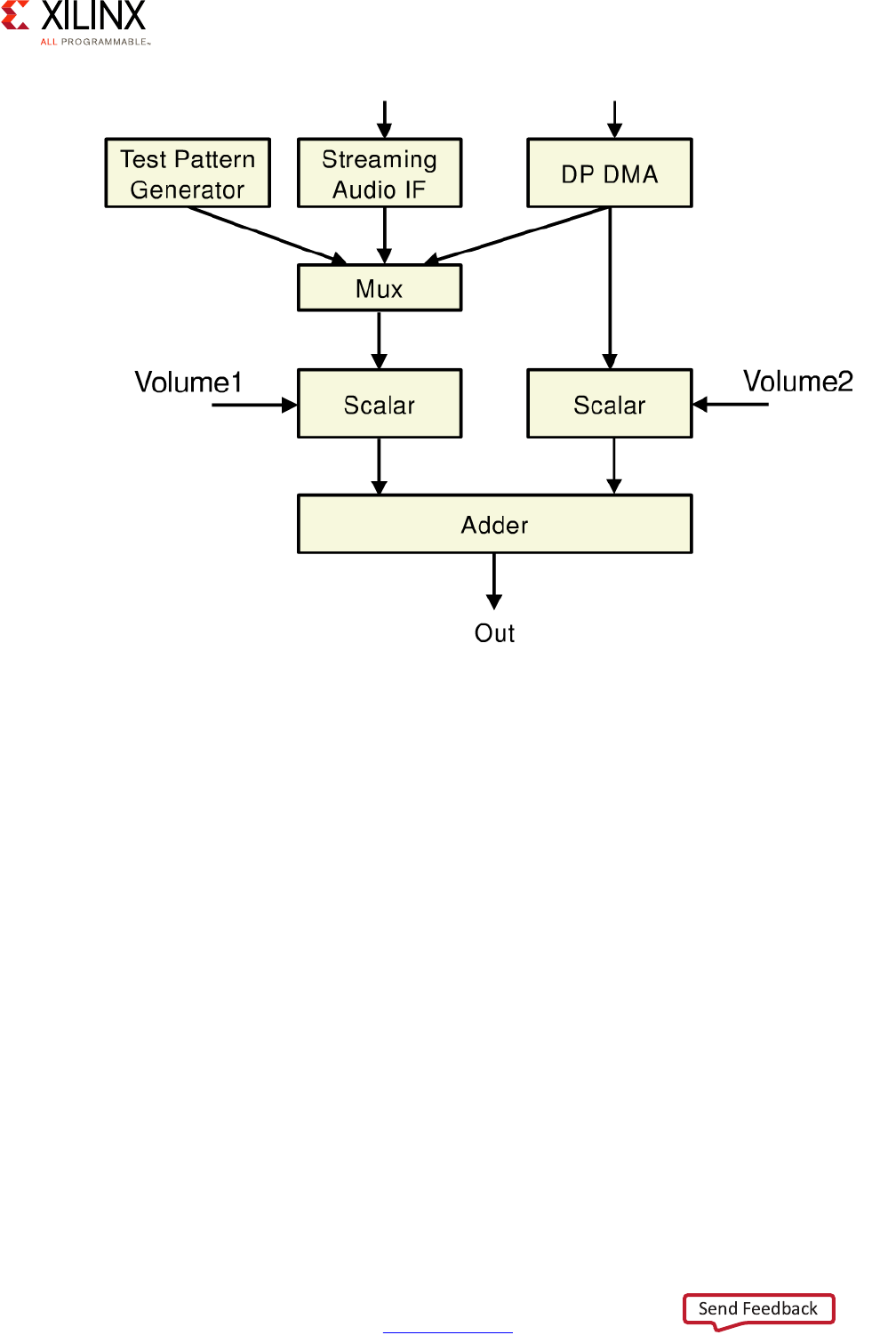
Zynq UltraScale+ MPSoC Embedded Design Methodology Guide 171
UG1228 (v1.0) March 31, 2017 www.xilinx.com
Chapter 9: Multimedia
DisplayPort DMA
The DPDMA controller handles up to 6 channels. Communication with the DDR controller is
conducted over a 128 bit AXI3 master port. The descriptor used by the DPDMA includes 16
different data words. Like the generic DMA descriptors for the DDR Controller, the DPDMA
descriptor includes a field to declare the size of the data pointed to by the descriptor
(XFER_SIZE) and a field for the address of the next descriptor (ADDR_NEXT). The descriptor
also includes several DisplayPort-specific fields meant to describe the data pointed to by
the descriptor: LINE_SIZE, STRIDE, TIME_STAMP_LSB, TIME_STAMP_MSB.
Linux DisplayPort Stack
As explained earlier in this chapter, the Zynq UltraScale+ MPSoC device's multimedia
support is Linux-centric. Figure 9-7 illustrates the Linux-based software stack made
available by Xilinx as part of its Linux packages for operating the DisplayPort.
X-Ref Target - Figure 9-6
Figure 9-6: MPSoC Display Controller Technical Module
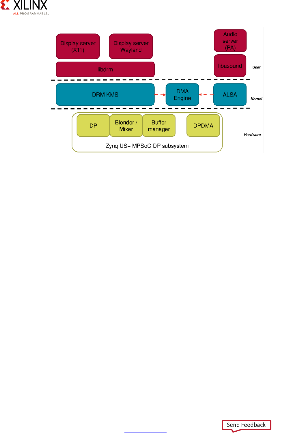
Zynq UltraScale+ MPSoC Embedded Design Methodology Guide 172
UG1228 (v1.0) March 31, 2017 www.xilinx.com
Chapter 9: Multimedia
The DisplayPort Subsystem Linux Stack consists of two layers on top of the DisplayPort
hardware:
• The bottom layer is a kernel layer that consists of the DRM, Kernel Mode Setting (KMS),
DMA Engine, and ALSA drivers.
°The Direct Rendering Manager (DRM) framework allows interfacing with graphics
hardware.
°The KMS driver is responsible for the display mode setting. It is the device driver for
a display controller.
°The DMA Engine enables DMA transfers.
°The Advanced Linux Sound Architecture (ALSA) provides device drivers and
low-level support for audio hardware.
• On top of the kernel level is the user level, which consists of libraries and servers.
°Libdrm is a user library that facilitates the interface of user space programs with the
DRM subsystem.
°Libasound is a user library that provides ALSA functions for application programs.
°The X11 Display Server provides the basic framework for a GUI environment to
move and draw windows on a display device as well as interaction with a mouse and
keyboard.
°The Wayland Display Server can be used as a replacement for the older X11 Display
Server.
°The PA Audio Server manages the use of and access to sound and audio devices
simultaneously by multiple audio applications.
X-Ref Target - Figure 9-7
Figure 9-7: DisplayPort Linux Software Stack
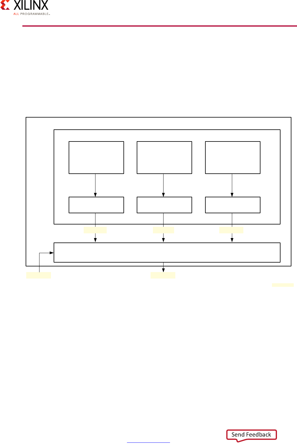
Zynq UltraScale+ MPSoC Embedded Design Methodology Guide 173
UG1228 (v1.0) March 31, 2017 www.xilinx.com
Chapter 9: Multimedia
GPU
The Zynq UltraScale+ MPSoC device's Graphics Processing Unit (GPU) is based on the ARM
Mali-400 MP2 architecture, providing 2D and 3D acceleration. As with the rest of the Zynq
UltraScale+ MPSoC device's multimedia capabilities, the GPU's operation is
Linux-dependent. OpenGL Graphics Libraries that support both OpenGLES1.1 and
OpenGLES 2.0 are available on the Linux platform for the Mali GPU for both X11 and FBDEV
Windowing systems. Figure 9-8 illustrates the GPU's block diagram.
The best way to get a sense of how the GPU itself operates and how it interacts with the rest
of the system is look at the data flow to and from the GPU, as can be seen in Figure 9-9.
X-Ref Target - Figure 9-8
Figure 9-8: Mali GPU Block Diagram
Geometry
Processor
MMU
AXI 64-bit
L2 Cache (64 KB)
Pixel
Processor
MMU
AXI 64-bit
Pixel
Processor
MMU
AXI 64-bit
AXI 128-bitAPB 32-bit
;
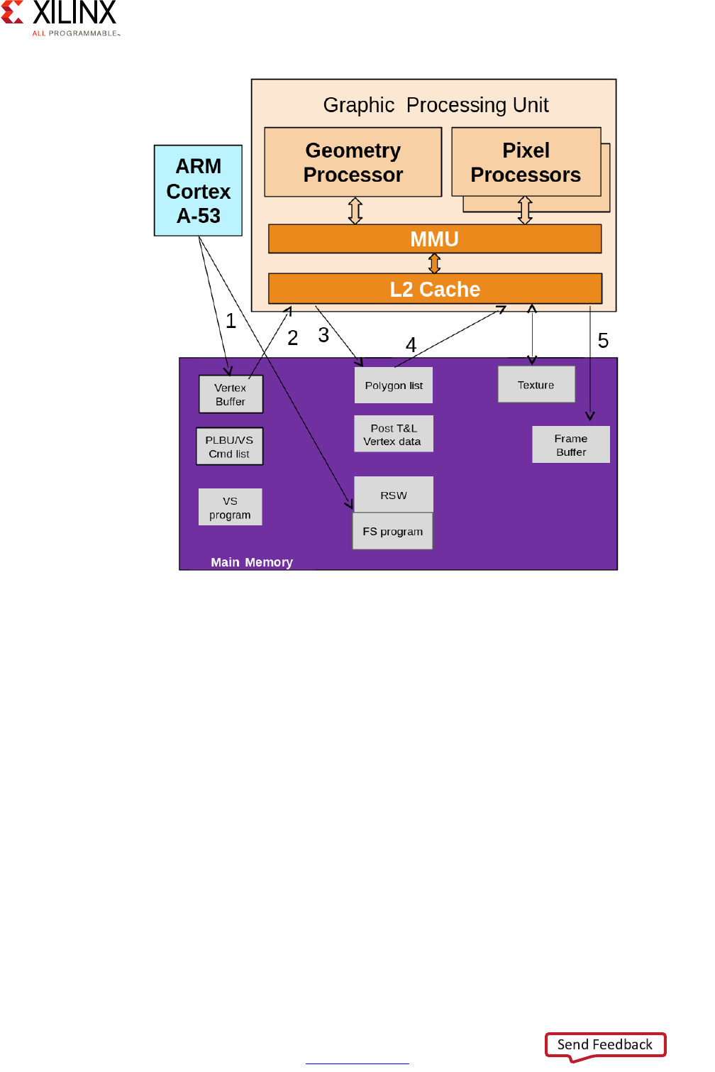
Zynq UltraScale+ MPSoC Embedded Design Methodology Guide 174
UG1228 (v1.0) March 31, 2017 www.xilinx.com
Chapter 9: Multimedia
In step #1, the software running on the APU uses the GL libraries to write vertices into the
vertex buffer in RAM. In step #2, those are loaded and processed by the geometry
processor and written as a polygon list in step #3. In step #4 the polygons are loaded by the
pixel processors along with textures and rendered as a final image to the frame buffer in
step #5.
The process by which the GPU operates is typically known as a rendering pipeline, where
several steps are involved for taking an initial data set from an application and rendering it
into an image to be displayed on screen. Modern GPUs are built on the concept of having
a programmable pipeline. The Zynq UltraScale+ MPSoC device GPU pipeline is
programmed through the GLSL API (OpenGL Shading Language) and can be illustrated in
Figure 9-10.
X-Ref Target - Figure 9-9
Figure 9-9: Simple View of Data Flow To and From the GPU
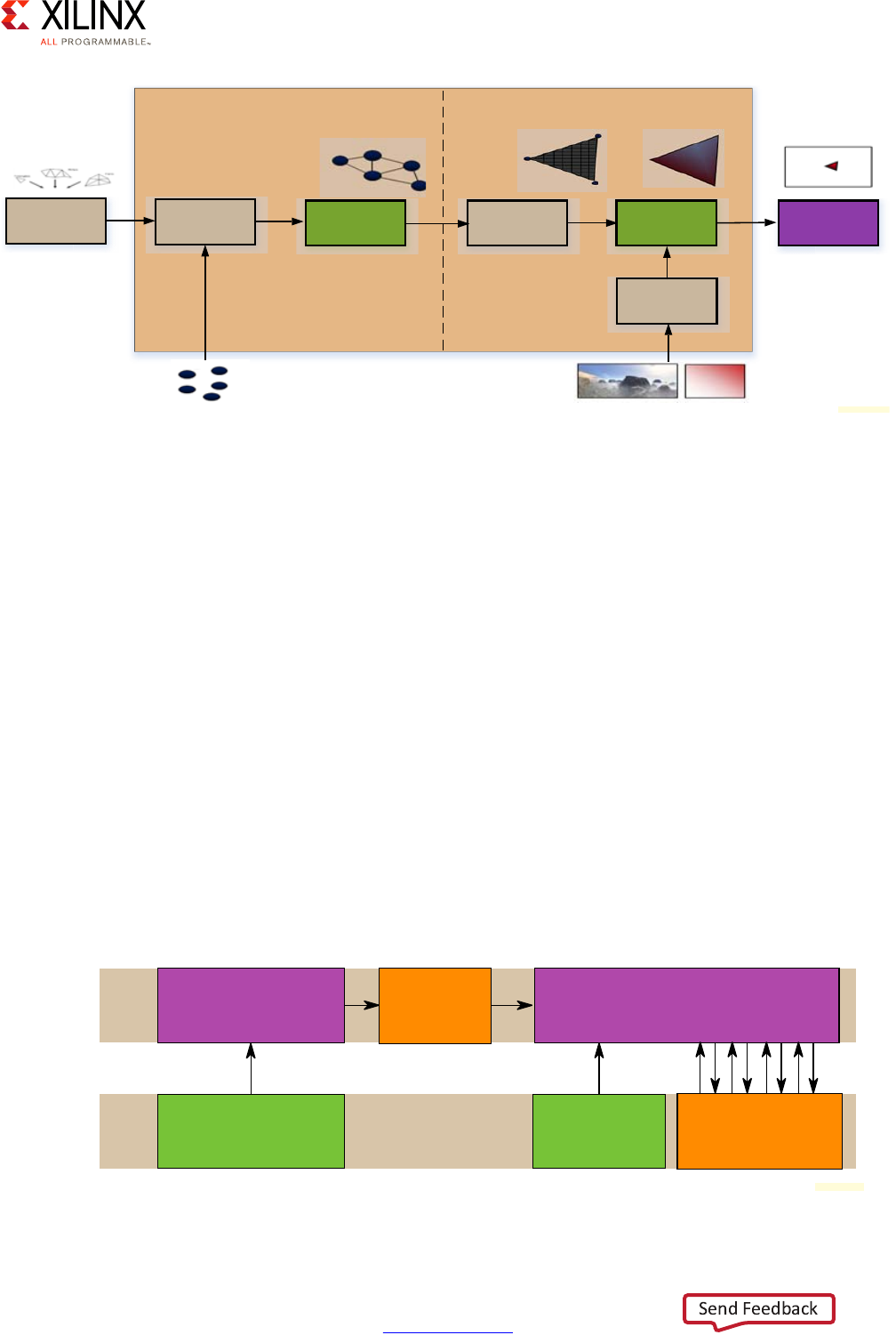
Zynq UltraScale+ MPSoC Embedded Design Methodology Guide 175
UG1228 (v1.0) March 31, 2017 www.xilinx.com
Chapter 9: Multimedia
Geometry processing stages operate on the raw vertex data sent by the application. As the
vertex shader is fed vertex attribute data as specified from a vertex array object by a
drawing command, it handles the processing of individual vertices and eliminates the
vertices that do not need to be displayed. Finally, it links them together to form primitives
that will be dealt with in the next stage. The rasterizer then takes the individual primitives
and breaks them down into discrete elements called fragments, based on the sample
coverage of the primitive. The fragment shader processes fragments generated by the
rasterizer into a depth value, a possible stencil value (unmodified by the fragment shader),
and zero or more color values, all of which are potentially written to the current frame
buffers.
As we saw in the data flow diagram earlier, there are several memory-to-GPU and
GPU-to-memory operations involved in enacting the different steps of the rendering
pipeline. In that regard, the Mali GPU features a tile-based renderer that reduces memory
transfers. To best understand the benefit of this tile-based renderer, we need to look at the
traditional way in which GPUs operate, the immediate mode. In an immediate mode
architecture, the vertices stored in memory are directly rendered one by one after
processing by a fragment shader; the fragment shaders are executed on each primitive, in
each draw call, in sequence as illustrated in Figure 9-11.
X-Ref Target - Figure 9-10
Figure 9-10: Zynq UltraScale+ MPSoC Device Mali 400-Based GPU Pipeline
Geometry Processing Pixels Processing
Application Vertex Setup Vertex Shader Rasterizer Fragment
Shader Frame buffer
Texturing
;
X-Ref Target - Figure 9-11
Figure 9-11: Immediate-Mode Renderer Data Flow
GPU Vertex Shader FIFO Fragment Shader
DDR Attributes Textures Framebuffer
Working Set
X18928-032117
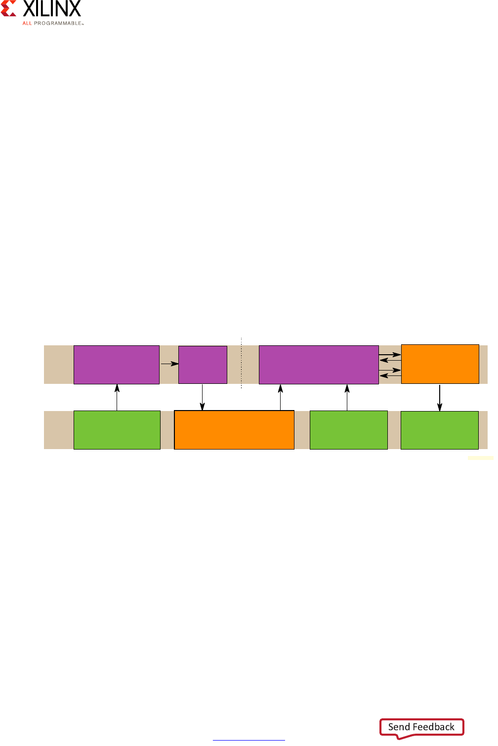
Zynq UltraScale+ MPSoC Embedded Design Methodology Guide 176
UG1228 (v1.0) March 31, 2017 www.xilinx.com
Chapter 9: Multimedia
Every blending, depth testing, and stencil testing operation requires the current value of
the data for the current fragment's pixel coordinate to be fetched from off-chip buffers in a
DRAM. At high resolutions the bandwidth load placed on system memory can be
exceptionally high, with multiple read-modify-write operations per fragment. The high
frequencies at which the GPU needs to work also requires the external memory to operate
at higher frequencies than regular system memory. Those considerations raise the GPU
energy demands.
The Mali GPU uses a different approach to minimize the amount of memory transactions
done during the rendering. Mali uses a tile-based rendering technique in which a tile is
usually a square area covering a number of pixels in the framebuffer. Tiles operated on are
held in an on-chip GPU memory buffer that holds the framebuffer contents for the tiles that
are currently being rendered. Tile-based rendering minimizes traffic to off-chip memory for
framebuffer contents, thereby reducing bandwidth and memory bus performance
requirements. ARM Mali uses a two pass rendering strategy as illustrated in Figure 9-12. It
first executes all geometry processing and then executes all the fragment processing in
another pass. During the geometry processing stage, Mali breaks the rendering area into
16x16 pixels tiles. The fragment shader cores process each tile to completion before moving
to the next one. In the case of the Mali 400, the two pixel processors can render two tiles at
once, improving the GPU throughput.
In addition to keeping the amount of transactions to external memory to a minimum, this
technique has another advantage. Namely, the locality of the tiles in the GPU's memory
makes it possible to apply several graphic algorithms in an efficient way, without having to
fetch vertex data from main memory.
Geometry Processor
Now that we've covered the GPU's overall functionality, let's take a closer look at the
geometry processor and its internal components as illustrated in Figure 9-13. The geometry
processor performs the data processing on the vertices to be rendered into images. As its
name imply, the geometry processor concerns itself with the image geometry, performing
mathematical operations on the data provided using the GL library APIs.
X-Ref Target - Figure 9-12
Figure 9-12: Tile-Based Renderer Data Flow
GPU Vertex Shader Tiler Fragment Shader
DDR Attributes
Local
Tile Memory
Geometry
Working Set Textures Compressed
Framebuffer
X18929-032117
Zynq UltraScale+ MPSoC Embedded Design Methodology Guide 177
UG1228 (v1.0) March 31, 2017 www.xilinx.com
Chapter 9: Multimedia
Vertex Shader
The first part of the geometry processor is the vertex shader core, which includes:
•Vertex Loader
°This is a DMA unit that loads the per-vertex data from the main system memory.
•Vertex Shader
°This module is responsible for conducting the calculations for each vertex. Its
output is used to build the polygon list that will be handled later in the pipeline.
• Vertex Storer
°The vertex storer stores data from the output registers of the Vertex Shader Core in
memory, The vertex storer can convert data from 32-bit floating point format to
fixed point or floating point formats of different sizes.
X-Ref Target - Figure 9-13
Figure 9-13: Mali GPU Geometry Processor Block Diagram
Geometry Processor
GPU
System Bus Interface
Vertex
Shader
Command
Processor
PLB
Command
Processor
PLB
Vertex Shader Core
Vertex Shader
Vertex
Storer
Vertex
Loader
Configuration Registers
MMU
L2
Cache
Pixel Processor
MMU
X15300-032817
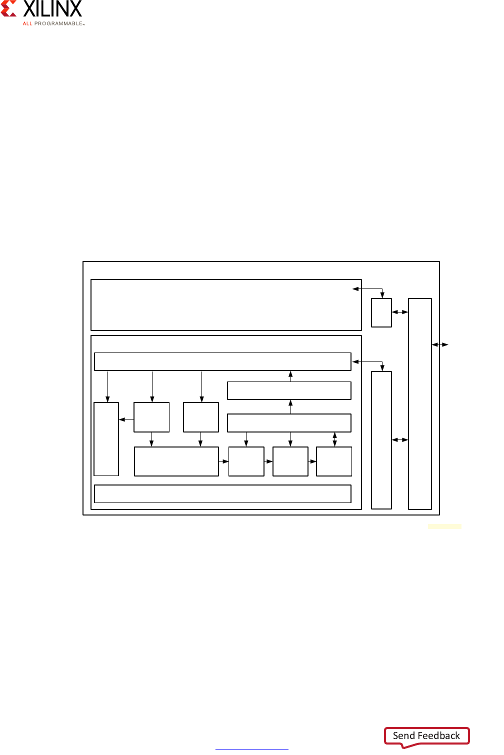
Zynq UltraScale+ MPSoC Embedded Design Methodology Guide 178
UG1228 (v1.0) March 31, 2017 www.xilinx.com
Chapter 9: Multimedia
Polygon List Builder
The Polygon List Builder (PLB) creates the list of polygons on which the pixel shader will
operate. As described earlier, the Mali GPU separates the rendering area in multiple tiles
and renders them tile by tile. The two pixel processors on the Zynq UltraScale+ MPSoC
device's Mali 400 each handle a pair of tiles in parallel. Before the pixel processors can do
their work, however, the PLB must generate the list of polygons to render in each tile and
discard some of them if they are hidden by other polygons.
Pixel Processor
Once the polygons have been prepared by the geometry processor, they are handed off to
the pixel processor which takes care of the fragment shader stage of the GPU pipeline.
Figure 9-14 illustrates each pixel processor's block diagram.
Each pixel processor operates as follows:
1. The Triangle Setup Unit builds up triangles given as input as a list of polygons generated
by the PLB.
2. The Rasterizer divides the input data into independent fragments. The fragments that
will end up rendered move to the next stages and those that are not going to be visible
are discarded.
3. The Fragment Shader Core calculates how each fragment from a primitive will look.
X-Ref Target - Figure 9-14
Figure 9-14: Pixel Processor Block Diagram
Geometry Processor
GPU
System Bus Interface
MMU
L2
Cache
Pixel Processor
MMU
Title Writeback Unit
Tile Buffers
Blending
Unit
Rasterizer Fragment
Shader
Configuration Registers
Vertex
Loader
Polygon
List
Reader
Triangle Setup Unit
RSW
X15302-091616
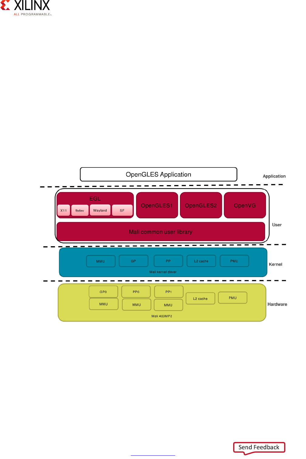
Zynq UltraScale+ MPSoC Embedded Design Methodology Guide 179
UG1228 (v1.0) March 31, 2017 www.xilinx.com
Chapter 9: Multimedia
4. The Blending Unit blends the calculated fragment into the tile buffer to produce the
final image. The way the fragment is blended is configurable: the fragment can be
opaque or be made partially transparent. Anti-aliasing, a way to make the image edges
look good in low resolution, is also applied at this stage.
5. The Tile Buffers module handles the completed tiles from the previous stages, performs
various tests on the fragments so that they are not uselessly rendered on screen.
6. The Write Back Unit writes the content of the tile buffer back to system memory.
Linux GPU Software Stack
As with the other multimedia components, the Zynq UltraScale+ MPSoC device's GPU
support is Linux-centric. Figure 9-15 illustrates the Linux-based software stack made
available by Xilinx as part of its Linux packages for operating the GPU.
The Linux GPU Software Stack has several layers:
• The lowest layer is the Mali Kernel Driver. This layer provides drivers for various
hardware components like the MMU, GP, PP, L2 Cache, and PMU.
• On top of the driver are user libraries:
°The Mali Common User Library contains libraries common to the GPU.
X-Ref Target - Figure 9-15
Figure 9-15: Linux GPU Software Stack
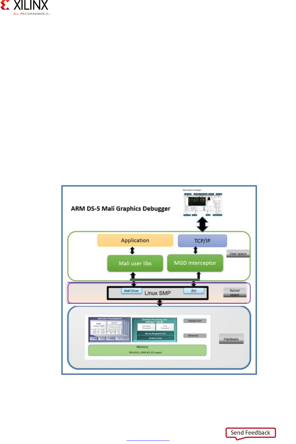
Zynq UltraScale+ MPSoC Embedded Design Methodology Guide 180
UG1228 (v1.0) March 31, 2017 www.xilinx.com
Chapter 9: Multimedia
°EGL is an interface between Khronos rendering APIs like OpenGL ES or OpenVG and
the underlying native platform window system. EGL handles graphics context
management, surface/buffer binding, rendering synchronization, and enables
high-performance, accelerated mixed-mode 2D and 3D rendering using other
Khronos APIs.
°Open Graphics Language (OpenGL) is an open industry standard API for 3D
graphics that handles hardware accelerated drawing of textured triangles. OpenGL
is basically a software interface to graphics hardware.
°OpenVG is an API designed for hardware-accelerated 2D graphics.
• At the top of the stack is the graphics application.
Debugging on ARM Mali GPU
The Mali Graphics Debugger (MGD) is a tool that can help developers using any Mali
hardware to debug the behavior of programs making use of the GPU. Figure 9-16
summarizes its operation.
The MGD will help developers understand the GPU operations their applications are doing:
X-Ref Target - Figure 9-16
Figure 9-16: Mali Graphics Debugger
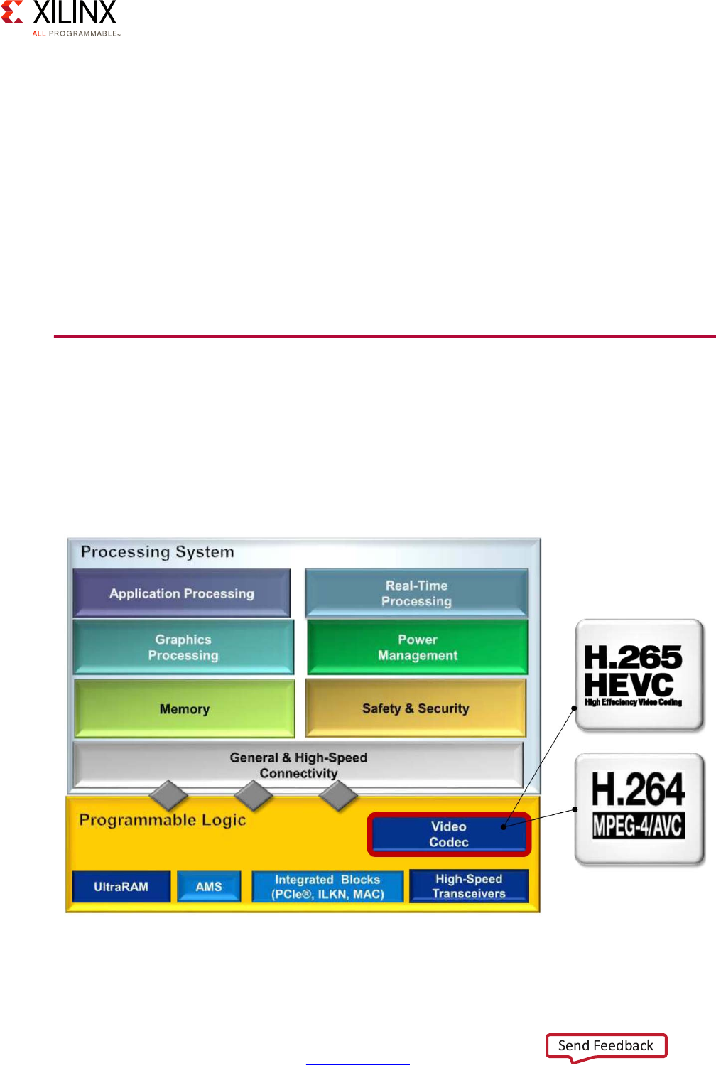
Zynq UltraScale+ MPSoC Embedded Design Methodology Guide 181
UG1228 (v1.0) March 31, 2017 www.xilinx.com
Chapter 9: Multimedia
• Allows draw call single stepping
• View texture usage
•Shader Statistics
•Vertex Attributes
•State View
•Dynamic Optimization Advice
Refer to the Zynq UltraScale+ MPSoC Graphics-GPU application debugging using ARM Mali
Graphics Debugger Tool Wiki page [Ref 19] for more information on using the MGD with the
Zynq UltraScale+ MPSoC device-based Xilinx® ZCU102 evaluation kit.
VCU
The Video Codec Unit (VCU) is included in the Programmable Logic (PL) in some variants of
the Zynq UltraScale+ MPSoC device. The VCU is especially suited in demanding video
applications where video data needs to be coded and decoded quickly. It supports
simultaneous decoding and encoding of H.264 and H.265 formats. Figure 9-17 provides a
high-level view of the VCU's location in the system.
X-Ref Target - Figure 9-17
Figure 9-17: Video Codec Unit's Location in the Zynq UltraScale+ MPSoC Device
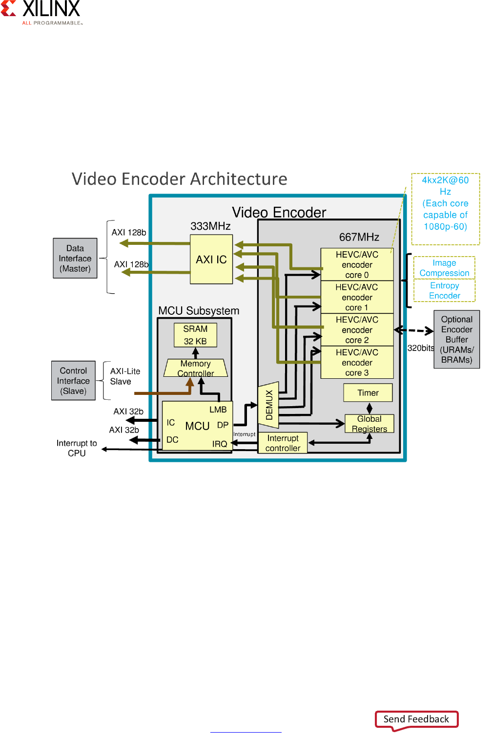
Zynq UltraScale+ MPSoC Embedded Design Methodology Guide 182
UG1228 (v1.0) March 31, 2017 www.xilinx.com
Chapter 9: Multimedia
The VCU features independent video encoding and decoding units. Each unit is controlled
by a Micro-Controller Unit (MCU) which controls the flow of data coming from the AXI
interface to be encoded or decoded. Commands are posted from the APU to the decoder or
encoder MCU units to deal with each frame, in the case of encoding, or each slices or tile,
in the case of decoding. The commands to the MCU can be posted through a register or be
copied in main memory where they will be read by the MCU.
The VCU's video encoder architecture is shown in Figure 9-18.
The VCU encoder unit has a single 32-bit slave AXI interface used by the APU to
communicate with the encoder unit to configure it and to start or stop encoding
operations. There are 2 AXI master interfaces to fetch the MCU instructions and another to
load/store additional MCU data. A pair of 128-bit AXI interfaces are used by the MCU to
extract the data to be encoded and to write back the encoded data. There are also extra
interfaces in the VCU to connect the encoder to the PL BRAM or UltraRAM blocks to be used
as needed. The VCU's video decoder architecture is shown in Figure 9-19.
X-Ref Target - Figure 9-18
Figure 9-18: VCU Video Encoder Architecture
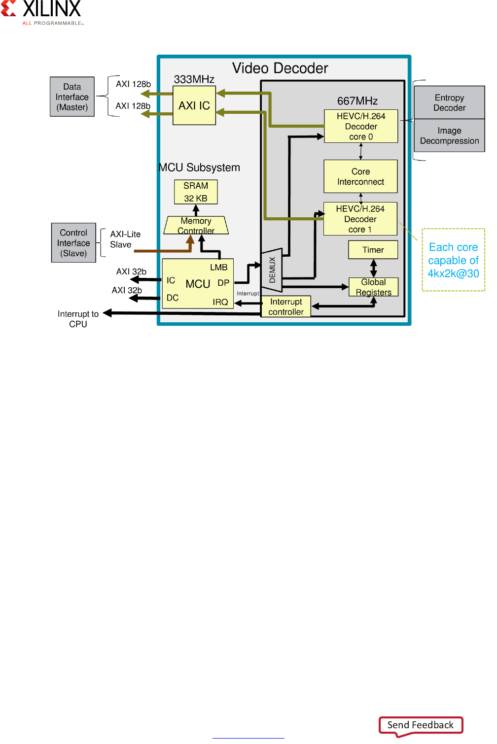
Zynq UltraScale+ MPSoC Embedded Design Methodology Guide 183
UG1228 (v1.0) March 31, 2017 www.xilinx.com
Chapter 9: Multimedia
The video decoder unit operates using a similar architecture to the encoding unit. As in the
case of the decoder, two AXI master interfaces fetch the data to decode and write the
decoded data to memory.
Note that the VCU can be set in low-latency mode, which diminishes the quality of the
compression but decreases the latency from input to codec or output from codec.
Memory Topology
As explained earlier, the VCU operates by retrieving and storing data to memory. As part of
the PL, the VCU can be configured to use memory through 3 different topologies. It can be
configured to:
1. Use DDR RAM through the DDR Controller
2. Interface with an external memory by using the Memory Interface Generator (MIG) in
the PL as described in Chapter 6, Memory.
3. Use a combination of the previous two.
All three configurations are illustrated in Figure 9-20 through Figure 9-22.
X-Ref Target - Figure 9-19
Figure 9-19: VCU Video Decoder Architecture
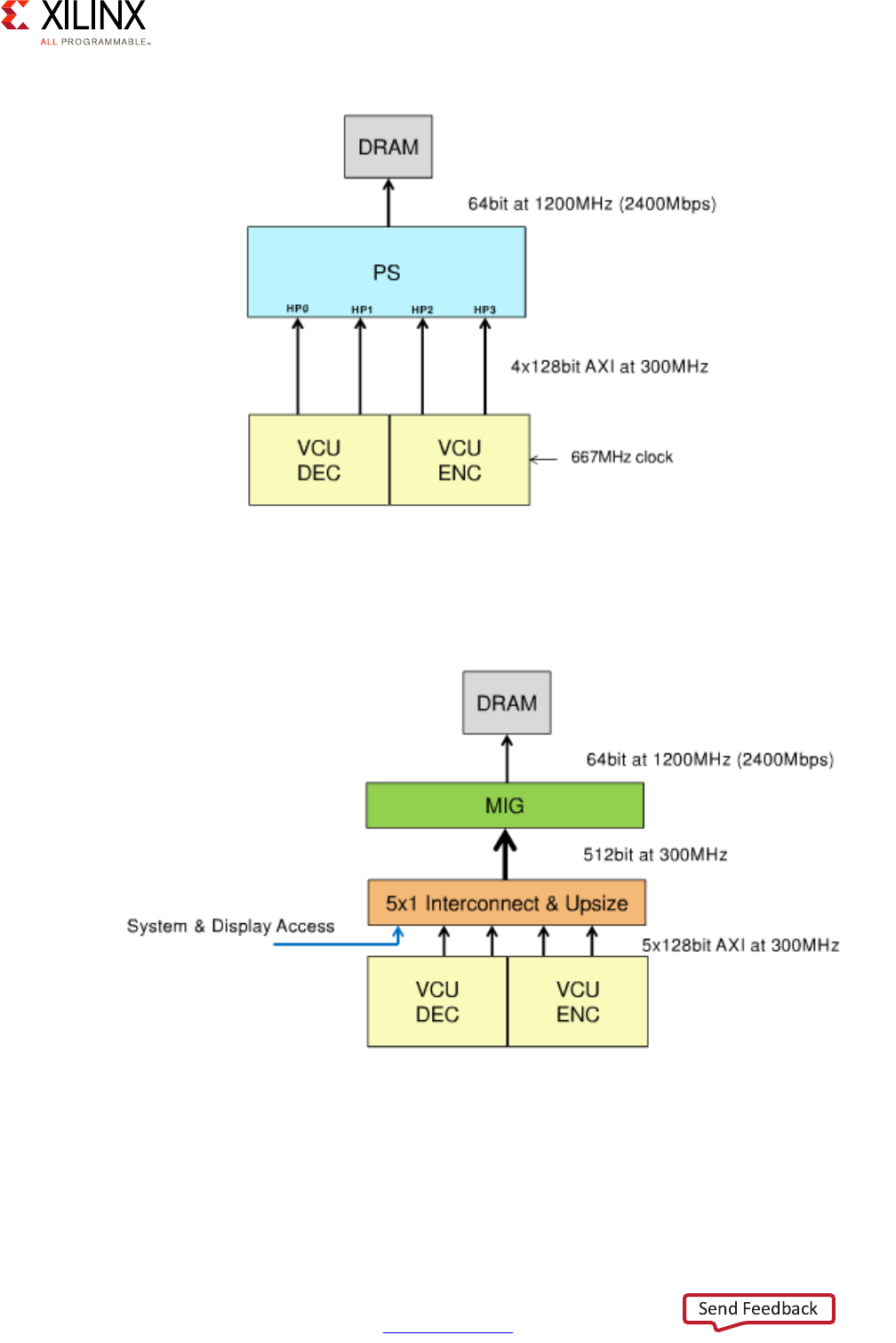

Zynq UltraScale+ MPSoC Embedded Design Methodology Guide 185
UG1228 (v1.0) March 31, 2017 www.xilinx.com
Chapter 9: Multimedia
As outlined earlier, memory bandwidth is the most important factor to keep in mind when
designing multimedia applications. Unlike the GPU and the DisplayPort, the VCU has the
option of using the PL's reconfigurable logic to extend its memory bandwidth by using an
in-PL memory controller to achieve higher memory bandwidth than is possible through just
the DDR Controller. Refer to Chapter 6, Memory for a discussion of memory bandwidth and
the options on how to tweak system design to your benefit if your design is
bandwidth-constrained.
X-Ref Target - Figure 9-22
Figure 9-22: VCU Using a Combination of DDR RAM and MIG in the PL

Zynq UltraScale+ MPSoC Embedded Design Methodology Guide 186
UG1228 (v1.0) March 31, 2017 www.xilinx.com
Chapter 9: Multimedia
Linux Video Codec Driver Stack
As with the previous multimedia components, the Zynq UltraScale+ MPSoC device's VCU
support is Linux-centric. Figure 9-23 illustrates the Linux-based software stack made
available by Xilinx as part of its Linux packages for operating the VCU.
The Linux Video Codec Driver Stack has several layers:
• At the lowest level on top of the hardware is the kernel space, which consists of the
Video for Linux 2 (V4L2) driver and the I/O Control (ioctl) kernel driver. The V4L2 is the
standard Linux kernel interface used for video capture. V4L2 contains specific interfaces
for selecting capture dimensions and color formats. It supports memory-to-memory
devices. It also provides common functions like memory allocation and buffering.
• The layer above the kernel space is the user space. This layer consists of
Gstreamer/Bellagio OMX IL and OpenMAX libraries:
°Gstreamer is a pipeline-based multimedia framework that links together various
media processing systems to complete complex workflows that, for example, read
data in as one format, process it, and then output the data in a different format. The
Bellagio OpenMAX Integration Layer (OMX IL) is a standard API that can access
hardware accelerators on platforms that provide them.
°The OpenMAX libraries are a set of cross-platform APIs for multimedia codec and
application portability.
• At the top of the stack is a video application.
X-Ref Target - Figure 9-23
Figure 9-23: Linux Video Codec Driver Stack
Video Application
Open MAX Implementation
Layer (OMX IL)
VCU Hardware
MCU Decoder
core
+
Decoder IP
MCU Encoder
core
+
Encoder IP
gstreamer
gstreamer OMX IL plugins
Driver APIs
Kernel Driver
(ioctl)
User space
Kernel space
Hardware
;

Zynq UltraScale+ MPSoC Embedded Design Methodology Guide 187
UG1228 (v1.0) March 31, 2017 www.xilinx.com
Chapter 10
Peripherals
The Zynq UltraScale+ device supports a very large number of peripherals that cater both for
legacy I/O interfaces such as I2C, serial peripheral interface (SPI) and general purpose I/O
(GPIO), and modern-day standards such as PCIe, SATA, and USB 3.0. While it is beyond the
scope of this guide to introduce you to or explain the peripheral interfaces supported by
the Zynq® UltraScale+™ device, this chapter will explain the specific way by which the
various peripherals are supported and what tradeoffs might be involved in their use.
Defining Your Peripherals Needs
Understanding your I/O needs is a fundamental part of your system design and will guide
you in selecting which of the peripheral I/O capabilities of the Zynq UltraScale+ device you
need to use. In that regard, there is nothing specific to the Zynq UltraScale+ device about
defining peripheral needs. As in the case of any other SoC, you must follow your
requirements.
There is one aspect where the Zynq UltraScale+ device does introduce an additional aspect
to analyze and that is the fact, as was explained in the Power Management chapter, that the
system blocks, including peripheral interfaces, are divided between 4 power domains.
Hence, when selecting which peripherals to use, you must keep in mind your power
management needs. Conversely, when designing power management for your system, you
will need to keep in mind which peripherals are needed and the power domain they belong
to.
The following questions are meant to help you in your process:
• Which peripherals do you need?
• Which power domain do they belong to?
• Do you have peripherals involved in system wakeup?
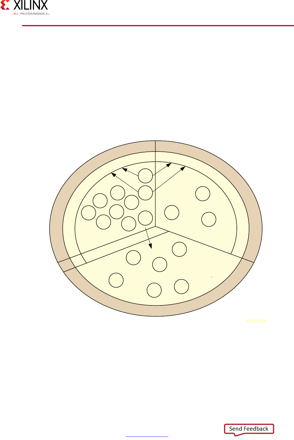
Zynq UltraScale+ MPSoC Embedded Design Methodology Guide 188
UG1228 (v1.0) March 31, 2017 www.xilinx.com
Chapter 10: Peripherals
Peripherals Methodology
As in other chapters, we will use a simplified view of the system to discuss the methodology
aspects surrounding the use of peripherals. The following figure focuses on presenting the
peripherals found within each power domain and their interaction with other power
domains. The external boundary of the device, i.e. where it is connected to the outside
world through the pins of the chip, is marked around the system with a gray background as
“Device Boundary”.
Note: This diagram does NOT attempt to precisely represent the internal blocks of the Zynq
UltraScale+ device. Instead, it is primarily a conceptual view for the purposes of the present
explanation.
As mentioned in the previous section, note that each peripheral belongs to a certain power
domain and that you will need to keep that in mind in designing your system.
X-Ref Target - Figure 10-1
Figure 10-1: Peripherals in Each Power Domain
Device Boundary
GigEth
USBNAND
GPIO
Quad-
SPI
SD/
eMMC
I2C
UART
CAN
SPI
Lower Power
Domain
PCIe
SATA
Display
Port
Full Power
Domain
GTH
Quad
Device Boundary
EMIO (Except USB, Quad-SPI and NAND)
MIO
PS-GTR
100G
Eth
PCIe
Gen4
Interlaken
VCU
Programmable
Logic Power
Domain
GTY
Quand
USB 3.0
ULPI
RGMII
SGMII
X18886-032017

Zynq UltraScale+ MPSoC Embedded Design Methodology Guide 189
UG1228 (v1.0) March 31, 2017 www.xilinx.com
Chapter 10: Peripherals
Another very important aspect to understand about the peripherals of the Zynq UltraScale+
device and the power domains they belong to is that each power domain has a different
way to connect its peripherals to the outside world. The low-power domain (LPD) relies on
the multiplexed IO (MIO) interface, the full-power domain (FPD) relies on the PS-GTR
interface and the programmable logic (PL) power domain (PLPD) relies on the configuration
of the PL to determine how the PL pins on the chip are connected. Generally speaking, the
LPD peripherals are considered low-speed peripherals, whereas the FPD peripherals are
considered high-speed peripherals.
The MIO interface multiplexes access to the 78 pins available for use by the LPD peripherals.
Pin function assignment is done through register programming on the MIO controller. This
is typically done using configuration code in the first-stage bootloader (FSBL) generated by
the Xilinx SDK tools, which is the recommended way to configure the MIO controller. The
Zynq UltraScale+ MPSoC Technical Reference Manual (UG1085) [Ref 7] provides detailed
descriptions of which pins can be used for which peripheral. As not all pins can be used for
all peripherals, you will need to carefully consider your peripheral needs versus the pins
available.
Given that the PL is reconfigurable, some of its boundary I/O pins can be configured to
serve for other purposes than just the IP in the PL. Namely, LPD peripherals can be routed
to the PL pins using extended multiplexed IO (EMIO), with some exceptions -- namely USB,
Quad-SPI, and NAND can’t be rerouted through EMIO. The specifics of the use of EMIO and
the limitations imposed on LPD peripherals routed through it are found in the Zynq
UltraScale+ MPSoC Technical Reference Manual (UG1085) [Ref 7]. However, using EMIO is
one way to circumvent any limitations your design may face in trying to use the available
MIO pins to accommodate your peripheral needs. EMIO can also be used as a way for AXI
masters to access IP found in the PL, though we suggest you refer to Chapter 5,
Programmable Logic to understand the options available to connect the IP found in the PL
to the rest of the system before deciding which to use.
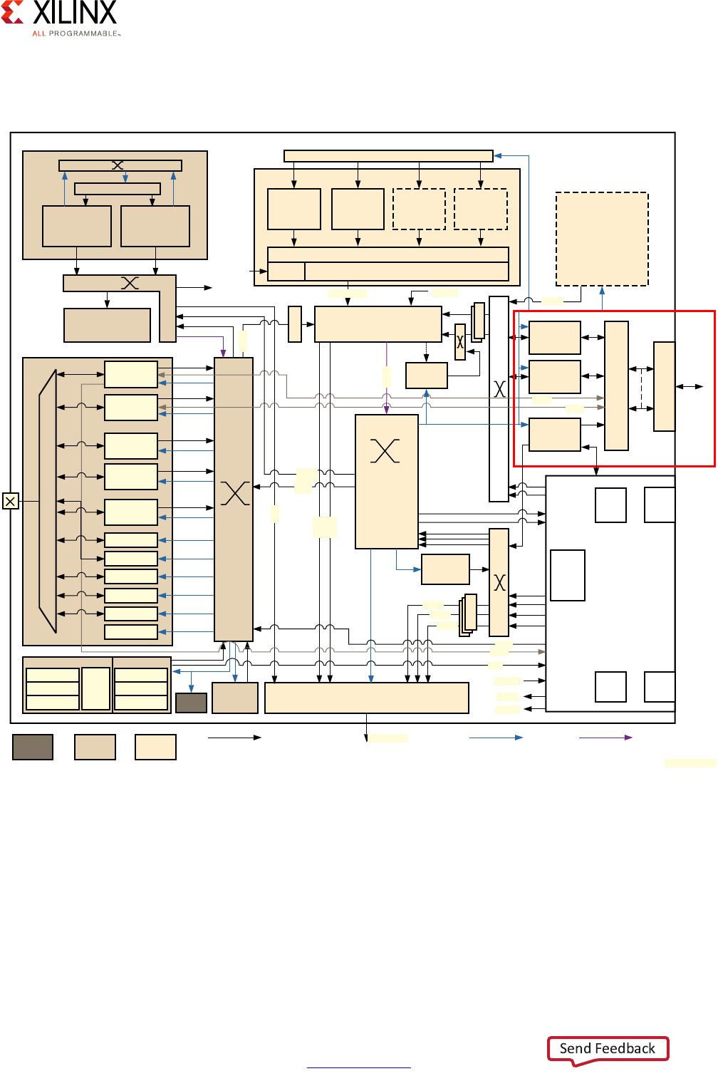
Zynq UltraScale+ MPSoC Embedded Design Methodology Guide 190
UG1228 (v1.0) March 31, 2017 www.xilinx.com
Chapter 10: Peripherals
The PS-GTR is part of the serial input output unit (SIOU) of the FPD as highlighted in red in
the following figure:
The PS-GTR transceiver of the FPD supports 4 multi-gigabit lanes providing external world
access to the FPD peripherals. The PS-GTR can also be used to provide connectivity for the
Gigabit Ethernet and USB functionality found in the LPD, thereby providing SGMI PHY
access and USB 3.0, respectively. The four different PS-GTR lanes operate at a frequency
between 1.25 Gbps and 6 Gbps. Each peripheral block that needs to interface through the
PS-GTR needs to be assigned one of the lanes of the PS-GTR by programming the PS-GTR
registers. As in the case of the MIO and the LPD peripherals, there are more peripheral
X-Ref Target - Figure 10-2
Figure 10-2: Serial Input Output Unit
CSU PSMU
RPU
GKv1
Cortex-R5
32K I/D Cache
128 KB TCM
Cortex-R5
32K I/D Cache
128 KB TCM
OCM
(256 KB)
To PL
From PL
APU
Cortex-A53
L1 I$/D$
GICv2
Cortex-A53
L1 I$/D$
Cortex-A53
L1 I$/D$
Cortex-A53
L1 I$/D$
SCU
ACP L2 with ECC [1MB]
128-bit ACE
CCI
TCU
Switch
FPD-
DMA
DDRC (DD3/4, LP DDR3/4)
Full
Power
Low
Power
Battery
Power
BPU
64-bit
PL-ACE
T
B
U
T
B
UPCIe Gen2
1/2/4
2 x SATA
v3.0
DisplayPort
v1.2 p1/3
Interconnect Matrix
PS-GTR
x4
128-bit
GPU
Mali-4 MP2
(64 KB L2)
PL
PCIe
GTH
or
GTY
AMS HD
I/O
Video
Codec
H.264/5
SGMII
USB3
128-bit
128-bit
128-bit
128-bit
To CCI
To ACP
From LP
64-bit
CFG
T
B
U
T
B
U
T
B
U
LPD-
DMA
128-bit
T
B
U
128-bit
64-bit
128-bit
128-bit
32 bit/64 bit
Processor
ROM 128 KB
RAM 32 KB
SHA
AES
RSA
Processor
ROM 128 KB
RAM 32 KB
SYSMON
EMIO
GPIOs
2x UART
2x I2C
2x CAN
2x SPI
QSPI
2x SDIO
SD3.0
NAND
ONFI 3.1
2x USB3
4 x GigaE
128
D
UL
PI
MS
Control Path
MS
Control Path/Datapath
MS
Datapath
MIO
SIOU
X18888-032117

Zynq UltraScale+ MPSoC Embedded Design Methodology Guide 191
UG1228 (v1.0) March 31, 2017 www.xilinx.com
Chapter 10: Peripherals
blocks connected to the PS-GTR than the PS-GTR can route simultaneously to the pins of
the device.
Hence, you must choose which peripherals you want to connect to the PS-GTR from the list
of peripherals found in the FPD and the LPD’s Gigabit Ethernet and USB functionality. In the
case of Gigabit Ethernet, you can always fall back to connecting to the Ethernet PHY using
RGMII instead of the SGMII available through PS-GTR. You can also use EMIO for the Gigabit
Ethernet but the connection then is GMII instead of RGMII or SGMII. In the case of USB, you
could route the USB block through MIO, though you’d be limited to ULPI.
Another power management-related aspect to keep in mind while designing your system
round peripherals is wake signals. Namely some of the Platform Management Unit (PMU)
General Purpose Inputs (GPIs) can be used for external wake signals. In addition, wake on
USB 2.0 and Ethernet is possible using ULPI and RGMII, respectively.
GPIO
The General Purpose I/O (GPIO) peripheral can be used to control the entire 78 pins
available through the MIO module. Through EMIO, the GPIO peripheral can also use up to
96 PL pins as input and 192 PL pins as output (96 as true outputs and the rest as output
enable). MIO-connected GPIO outputs are 3-state capable -- i.e. low, high or
high-impedance. The figure below is a block diagram of the GPIO peripheral and its
interaction with the MIO module and the PL through EMIO.
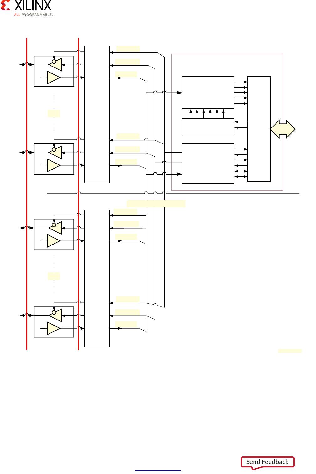
Zynq UltraScale+ MPSoC Embedded Design Methodology Guide 192
UG1228 (v1.0) March 31, 2017 www.xilinx.com
Chapter 10: Peripherals
The GPIO pin functions can be programmed individually or as a group. The pins are
grouped into 6 banks, numbered from 0 to 5. Banks 0 to 2 are accessible through the MIO
interface and banks 3 to 5 are accessed through the EMIO interface. The following figure
illustrates the banks of the GPIO peripheral.
X-Ref Target - Figure 10-3
Figure 10-3: GPIO Interaction with MIO and PL Through EMIO
APB Interface
APB
Event Detector
Configuration
Registers
PL
MIO
Pins
Pins
PS
GPIO Module
EMIO Interface to PL
gpio_in[n]
gpio_out[n]
gpio_oe[n]
gpio_in[0]
gpio_out[0]
gpio_oe[0]
gpio_in[n]
gpio_out[n]
gpio_oe[n]
gpio_in[0]
gpio_out[0]
gpio_oe[0]
X18889-032017
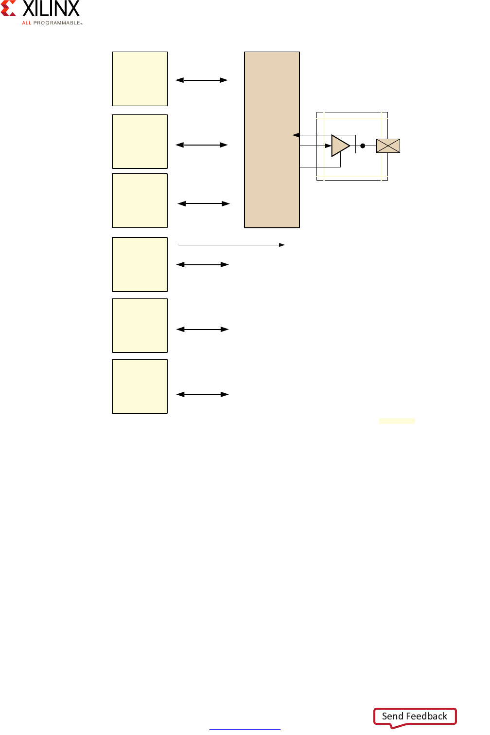
Zynq UltraScale+ MPSoC Embedded Design Methodology Guide 193
UG1228 (v1.0) March 31, 2017 www.xilinx.com
Chapter 10: Peripherals
Interrupts can be triggered on the pins using customizable sensitivity:
• Level-sensitive: high or low
• Edge-sensitive: positive, negative or both
X-Ref Target - Figure 10-4
Figure 10-4: GPIO Banks
GPIO
Bank 0
MIO
26-bit
GPIO
Bank 1
26-bit
GPIO
Bank 2
26-bit
Pin
x78
32-bit
EMIOGPIOI[95;64]
EMIOGPIOO[95;64]
EMIOGPIOTN[95;64]
EMIO Interface to PL
EMIOGPIOI[31:0]
EMIOGPIOO[31:0]
EMIOGPIOTN[31:0]
32-bit
EMIOGPIOI[63:32]
EMIOGPIOO[63:32]
EMIOGPIOTN[63:32]
32-bit
GPIO
Bank 3
GPIO
Bank 4
GPIO
Bank 5
X18890-032017X18891-032017
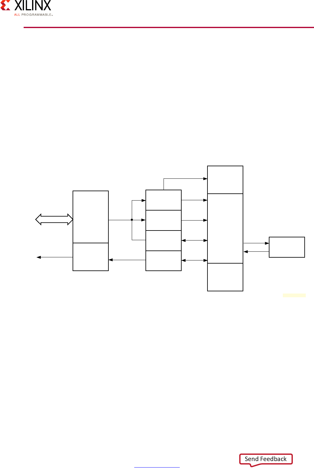
Zynq UltraScale+ MPSoC Embedded Design Methodology Guide 194
UG1228 (v1.0) March 31, 2017 www.xilinx.com
Chapter 10: Peripherals
I2C
I2C is a simple 2 wire bus designed to interface with low speed peripherals. Of the two
wires, one is the data line (SDA) and the other is used to drive the clock signal (SCL). The
nodes on the I2C bus can be one of master or slave. The master node is responsible for
driving the clock signal of the bus and initiates communication with the slave nodes. The
slave nodes are responsible for receiving the clock signal and answering the requests of the
master. The I2C protocol also allows for multiple masters which need to be aware of the
other masters and not use the I2C bus when another master is currently using it.
The Zynq UltraScale+ device includes an I2C controller module that can work in both master
or slave mode in a multi-master design. The figure below is a block diagram of the I2C
controller found in the Zynq UltraScale+ device.
The controller can be set to act as a master node or a slave node through register
programming. Also, the controller can be used in polling mode and interrupt-driven mode.
X-Ref Target - Figure 10-5
Figure 10-5: I2C Block Diagram
APB
Interface
Interrupts
Interrupts
APB
Status
Register
RX Data
Register
TX Data
Register
Control
Register
Control
FSM
RX Shift
Register
Clock
Enable
Generator
SCL/SDA
Interface
X18892-032017
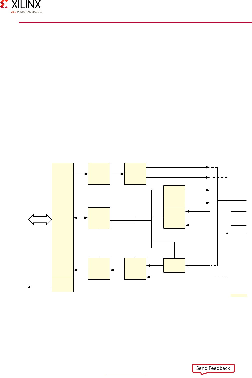
Zynq UltraScale+ MPSoC Embedded Design Methodology Guide 195
UG1228 (v1.0) March 31, 2017 www.xilinx.com
Chapter 10: Peripherals
SPI
The Serial Peripheral Interface bus (SPI) can be used for higher speed communication
between electronic components than I2C. The nodes on the SPI bus can be one of master or
slave. There can be multiple masters. The protocol uses 4 wires for communication.
• MOSI: Master Output -> Slave Input
• MISO: Master Input -> Slave Output
• SCLK: Serial Clock
• SS: Slave Select
The MOSI and MISO signals are used for full duplex communication between master and
slaves. The Zynq UltraScale+ device includes 2 identical SPI controllers that can be
independently and simultaneously controlled and operated by the corresponding software
drivers. The figure below is a block diagram of the SPI controllers of the Zynq UltraScale+
device.
X-Ref Target - Figure 10-6
Figure 10-6: SPI Controller Block Diagram
TX FIFO
MI
APB
Interface
Transmit
SPI CTRL
RX FIFO
SPI
Master
SPI
Slave
Receive
Slave
Sync
SO
SS[2:0]
SCLK
SCLK
SS
SI
Interrupt Interrupts
MO
MOSI
SPI
Interface
Pins
MOSI
SCLK
SS
MISO
APB
X18893-032017

Zynq UltraScale+ MPSoC Embedded Design Methodology Guide 196
UG1228 (v1.0) March 31, 2017 www.xilinx.com
Chapter 10: Peripherals
The SPI controllers of the Zynq UltraScale+ device can be set in one of three modes:
• Slave Mode—In this mode the other masters connected to the SPI bus drive the
controller clock.
• Master Mode—In this mode the SPI controller will manage the slave nodes’ clock. The
controller can decide which slave to talk to by manipulating the SS line.
• Multi-Master Mode—In multi-master mode the controller needs to be disabled
between transfers in order not to conflict with the other masters. The controller can
detect if another controller uses the bus by monitoring the SS signal.
The SPI controllers do not support direct memory access (DMA). Hence the communication
is done through register reads and writes to the controller AXI interface. The FIFOs (TX and
RX) in the controller are 128 bytes deep. To transfer data to a slave, the master writes data
in the TXFIFO using the relevant registers. To read data from a slave, the master reads from
the RXFIFO. For every byte written to TXFIFO, a byte is stored in RXFIFO. For every n bytes
written to the TXFIFO, there are n bytes stored in RXFIFO that must be read by software
before starting the next transfer.
The controller can be configured to automatically control the slave selection line during
data transfer or leave the control to software. In the latter mode, the manual mode, SPI
software has to set a register to enable the SS line.
UART
The Universal Asynchronous Receiver/Transmitter (UART) is a simple protocol for
asynchronous serial communication. The format and transmission speed of the
communication between two UART modules is configurable but needs to be specified
before the communication is established.
The UART in the Zynq UltraScale+ device supports a wide variety of parameters:
• programmable baud rate
• 6, 7, or 8 data bits
• 1, 1.5, or 2 stop bits
• Odd, even, space, mark, or no parity
Note: Refer to the Zynq UltraScale+ MPSoC Technical Reference Manual (UG1085) [Ref 7] for a full
list of parameters.
Those parameters can be changed through registers specific to the UART controller.
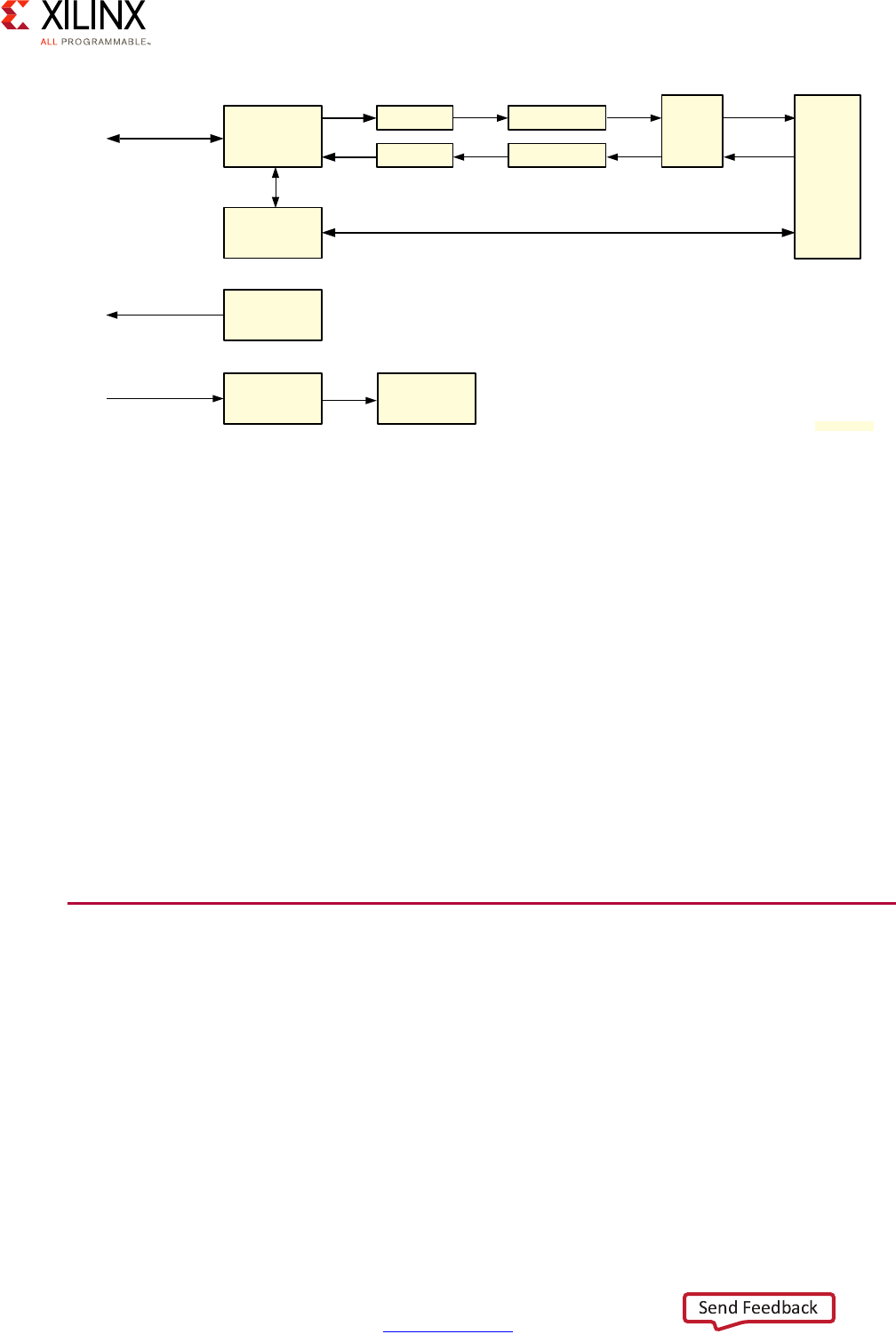
Zynq UltraScale+ MPSoC Embedded Design Methodology Guide 197
UG1228 (v1.0) March 31, 2017 www.xilinx.com
Chapter 10: Peripherals
The controller is divided into 2 parts: reception (RX) and transmission (TX). Each path
includes a 64 byte FIFO buffer.
The UART controller can be set to 4 different modes. Three of them are useful for
application or hardware testing.
• The Normal Mode is used for standard UART operations.
• In Automatic Echo Mode the data received on the RxD is routed to the receiver and the
TxD pin.
• In Local Loopback Mode the data sent through the UART controller is looped back to
the receiver side. Hence, any data sent is received as-is by the controller.
• In Remote Loopback Mode the RxD signal is connected to the TxD signal. In this mode
the controller cannot send any data. This mode can be used for testing remote/host
channel UART receiver and transmitter operation.
CAN Controller
The controller area network (CAN) bus is a standard used in the automotive industry to
facilitate the communication between devices in a car. The Zynq UltraScale+ device includes
two separate CAN controllers: CAN0 and CAN1. As with other LPD peripherals, the CAN
controllers operate through the MIO subsystem or EMIO to connect outside of the device
boundary. The CAN controllers’ clock source can be set to use an internal clock or it can be
driven by an external clock. The CAN controller system view is presented below.
X-Ref Target - Figure 10-7
Figure 10-7: UART Controller
APB
Slave
Interface
PS AXI
Interconnect
Control and
Status Register
Interrupts
Interrupt
Controller (GIC)
Optional
Divide by 8
UART
Reference Clock
TXFIFO
RXFIFO
Transmitter
Receiver
Mode
Switch MIO/EMIO
EMIO
CTS, RTS, DSR, DCD, RI, DTR
UART TxD
UART RxD
Baud Rate
Generator
X18898-032017
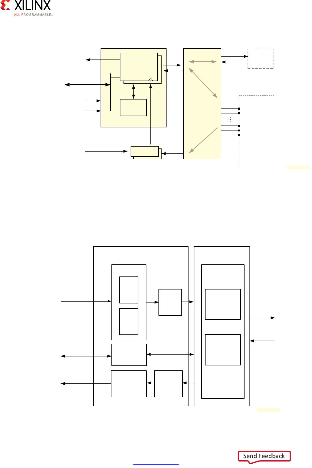
Zynq UltraScale+ MPSoC Embedded Design Methodology Guide 198
UG1228 (v1.0) March 31, 2017 www.xilinx.com
Chapter 10: Peripherals
The figure below illustrates the block diagram of the CAN controller. A separate storage
buffer exists for transmission and reception of data. The two FIFO buffers (TXFIFO for
transmit and RXFIFO for reception) can hold up to 64 messages at once. Each controller also
includes a special buffer for high priority outbound messages, TXHPB. The messages in this
buffer will preempt the messages which would normally be sent via the TXFIFO.
X-Ref Target - Figure 10-8
Figure 10-8: CAN Controller System Viewpoint
X-Ref Target - Figure 10-9
Figure 10-9: CAN Controller Block Diagram
CAN
Controllers
PL
Clock
TX, RX
TX, RX
Clocking
CAN{0,1} REF clock
CAN{0,1] CPU_1x clock
IRQ ID# {60,83}
MIO-EMIO
Routing
EMIO
MIO
Pins
Device
Boundary
TX, RX
External
Clock
Source
Control
Registers
APB
Interconnect
Slave
Port
CAN{0,1] CPU_1x reset
X18897-032017
Object Layer – Data Buffer and Filtering Transfer Layer
Protocol Engine
Bit Stream
Processor
Bit Timing
Logic
TX
FIFO
TX
HPB
TX
Priority
Logic
TX Storage
Configuration
Registers
RX
FIFO
Acceptance
Filtering
CAN TX
CAN RX
Data Read
Register R/W
Data Write
APB
Interface
X18899-032017
Zynq UltraScale+ MPSoC Embedded Design Methodology Guide 199
UG1228 (v1.0) March 31, 2017 www.xilinx.com
Chapter 10: Peripherals
Message Filtering
On the receiving side, a user-defined Acceptance Filter will determine which incoming
message gets put in the RXFIFO. The acceptance filters include a mask and an ID which
determines whether to pass the message further up the stack or to acknowledge and
discard them.
The filter module can hold 4 different acceptance filters. Each of them can be individually
disabled or enabled through register configuration. When a frame is received, the mask and
the ID stored and each enabled acceptance filter is compared against the ID and the mask
in the message. The message is accepted if any of the filter matches the corresponding data
in the message.
CAN Controller Modes
The CAN controller can be put in any of 5 modes. The transition between the modes must
be done according to the state machine below.
Configuration Mode
This is the mode the controller is in after reset. As can be seen on the state machine above,
putting the controller in one of the diagnostics modes requires going through the
Configuration Mode first.
X-Ref Target - Figure 10-10
Figure 10-10: CAN Operating Mode Transitions, Mode Settings
Configuration
Reset
Normal
Sleep
Loopback
Snoop
Reset
can.SRR[CEN]=0
Diagnostics
CRL_APB.RST_LPD_IOU2 [CANx_RESET] = 0
Reset:
CRL_APB.RST_LPD_IOU2 [CANx_RESET]=1
OR
can.SRR[SRST}=1
(Self-clearing)
Hardware Forces
can.SRR[CEN]=0
X18900-032117

Zynq UltraScale+ MPSoC Embedded Design Methodology Guide 200
UG1228 (v1.0) March 31, 2017 www.xilinx.com
Chapter 10: Peripherals
Normal Mode
In this mode messages are sent through the TX line and received on the RX line per the CAN
controller specification.
Sleep Mode
This mode can be used to save a small amount of power during the idle times for the
controller. When in sleep mode, the controller transitions to the normal mode when it
receives data and when it is asked to send data.
Loopback Mode (Diagnostics)
In Loopback Mode, the controller will automatically receive everything it transmits. It won’t
receive any messages from other nodes in the CAN network.
Snoop Mode (Diagnostics)
In Snoop Mode, the controller does not transmit anything but will receive the messages
sent by the other nodes of the system.
Interrupts
The CAN controller is connected to the generic interrupt controller (GIC). Each CAN
controller uses a different interrupt number, 55 for CAN0 and 56 for CAN1. There are several
sources of interrupts but they can be grouped into these 4 categories:
•TXFIFO and TXHPB
•RXFIFO
• Message passing and arbitration
• Sleep mode and bus-off state

Zynq UltraScale+ MPSoC Embedded Design Methodology Guide 201
UG1228 (v1.0) March 31, 2017 www.xilinx.com
Chapter 10: Peripherals
NAND
The Zynq UltraScale+ device includes a NAND memory controller complying with the ONFI
3.1 specification. As shown in the figure below, the controller includes an error-correcting
code (ECC) interface supporting single-level cell (SLC) and multi-level cell (MLC) error
correction as specified in the ONFI specification.
The NAND controller includes an AXI slave and an AXI master interface. The AXI slave
interface is used to interface with the Control Registers and therefore enables an AXI master
to control the NAND flash interface. During DMA transfers, be they read or write, the AXI
master interface of the NAND controller is used to write or read from memory to the flash
through the dual-ported RAM.
X-Ref Target - Figure 10-11
Figure 10-11: NAND Flash AXI Functional Block Diagram
ARM
Processor
AXI
Master
Interface
AXI
Slave
Interface
Dual-Port
RAM
Control
Registers
NAND
Flash
Interface
ECC
Flash
Memory 0
Flash
Memory 1
Flash
Memory 2
Flash
Memory 3
AXI Bus
NAND Flash Bus
(8-Bit)
X18901-032017

Zynq UltraScale+ MPSoC Embedded Design Methodology Guide 202
UG1228 (v1.0) March 31, 2017 www.xilinx.com
Chapter 10: Peripherals
SD/SDIO/eMMC
The SD controller gives access to various SD formats such as SD cards, MMC and eMMC
devices.
The SD card is accessible through an AXI slave interface by the rest of the system. Much like
in the case of the NAND controller, the AXI master interface in the controller is used for
DMA requests.
SD/SDIO/eMMC DMA
The SDIO controller complies with the SD Controller Specification and implements DMA as
defined in the specification. The specification defines two DMA interfaces. One is called
ADMA (advanced DMA) and the other is called SDMA (single operation DMA). The Zynq
UltraScale+ device controller supports both DMA modes.
SDMA
SDMA does not use a descriptor but uses a single address for reads or writes. The SD card
controller expects the address of the transfer, the number of blocks and the size of the
blocks to copy to be passed in its registers. The controller triggers an interrupt to get the
application to update the data source register after each block is transferred. For large
transfers this makes the CPU a bottleneck and limits the performance of SDMA. ADMA is
therefore the preferred way to do DMA with the SD controller.
The steps required for proper use of SDMA are described in the SD Host Controller
Specification 1.0.
X-Ref Target - Figure 10-12
Figure 10-12: SD/SDIO/eMMC Controller Block Diagram
AXI
Master
AXI
Target
PIO/DMA
Controller
Host Control
Register
Set
Block
Buffer
FIFO
(Configurable)
SD
Interface
Controller
TX Clock
Delay
(DLY_BUF/
DLL)
TX
Flip-Flops
RX
Flip-Flops
RX Clock
Delay
(DLY_BUF/
DLL)
SD
TUNING
SD
RECV_CTRL
SD
CMD_CTRL
SD
XMIT_CTRL
SD
TIME_OUT
SD
CARD_DET
SD
CLK_GEN
SD Host Control Block
Master
Interface
Target
Interface
SD
Interface
X18902-032017
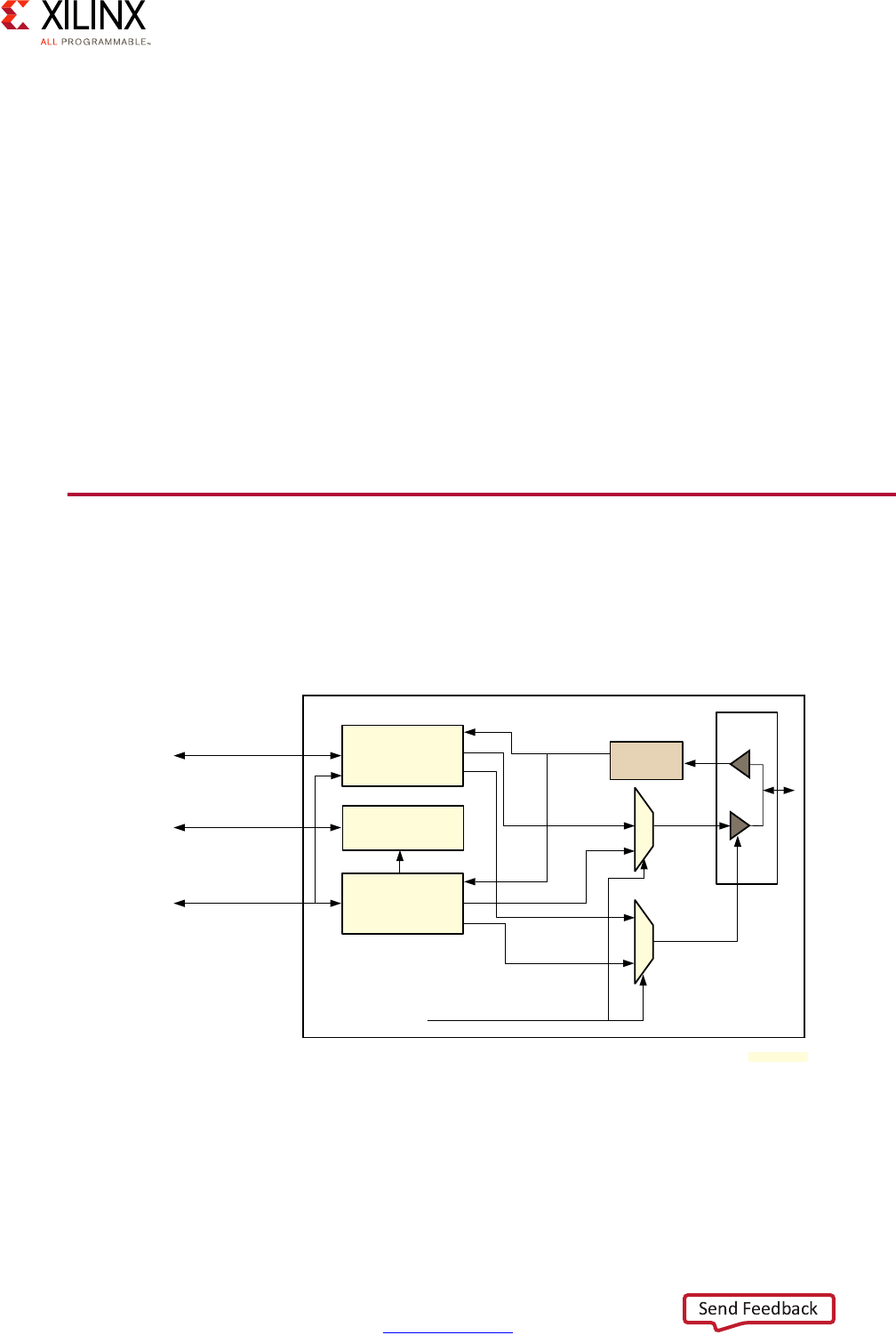
Zynq UltraScale+ MPSoC Embedded Design Methodology Guide 203
UG1228 (v1.0) March 31, 2017 www.xilinx.com
Chapter 10: Peripherals
ADMA
The SD specification for ADMA describes a DMA descriptor similar to the hybrid descriptor
supported by system wide Scatter-Gather DMA. With ADMA, multiple transactions can be
handled by the controller without the CPU needing to be interrupted, unlike with SDMA.
ADMA is supported in 2 versions. ADMA1 only supports transfer size of 4KB while ADMA2
supports any transfer size. Both versions of the ADMA protocols are described in the SD
Host Controller Specification version 3.0.
SD/SDIO/eMMC PIO
The SDIO controller also offers a Programmed IO (PIO) interface which enables direct access
to the internal transfer buffer through the registers of the controller. PIO mode requests go
through the slave interface of the controller and thus can be a way to enact SD transfers
without DMA.
Quad-SPI
The Quad-SPI controller of the Zynq UltraScale+ device includes two types of controllers,
the Generic Quad-SPI Controller and the Legacy Quad-SPI controller. The figure below
provides the Quad-SPI controller block diagram.
Switching between the two controllers can be done through register programming. The
Legacy Quad-SPI controller is important in the boot process because it supports eXecute In
Place (XIP) which can be useful during the first stages of the boot process. See the Memory
Chapter for more information about how XIP can be used during the boot process.
X-Ref Target - Figure 10-13
Figure 10-13: Quad-SPI Controller Top Level Block Diagram
DMA
AXI Master
Write I/F
AXI Slave
Read I/F
Generic
Quad-SPI
Controller
APB Slave
I/F
Legacy
Quad-SPI
Controller
RX Capture
and
Delay Line
DIN
DOUT
OEN
DIN
DOUT
OEN
I/O
Logic
DOUT
DOUT
OEN
generic_qspi_en
X18903-032017
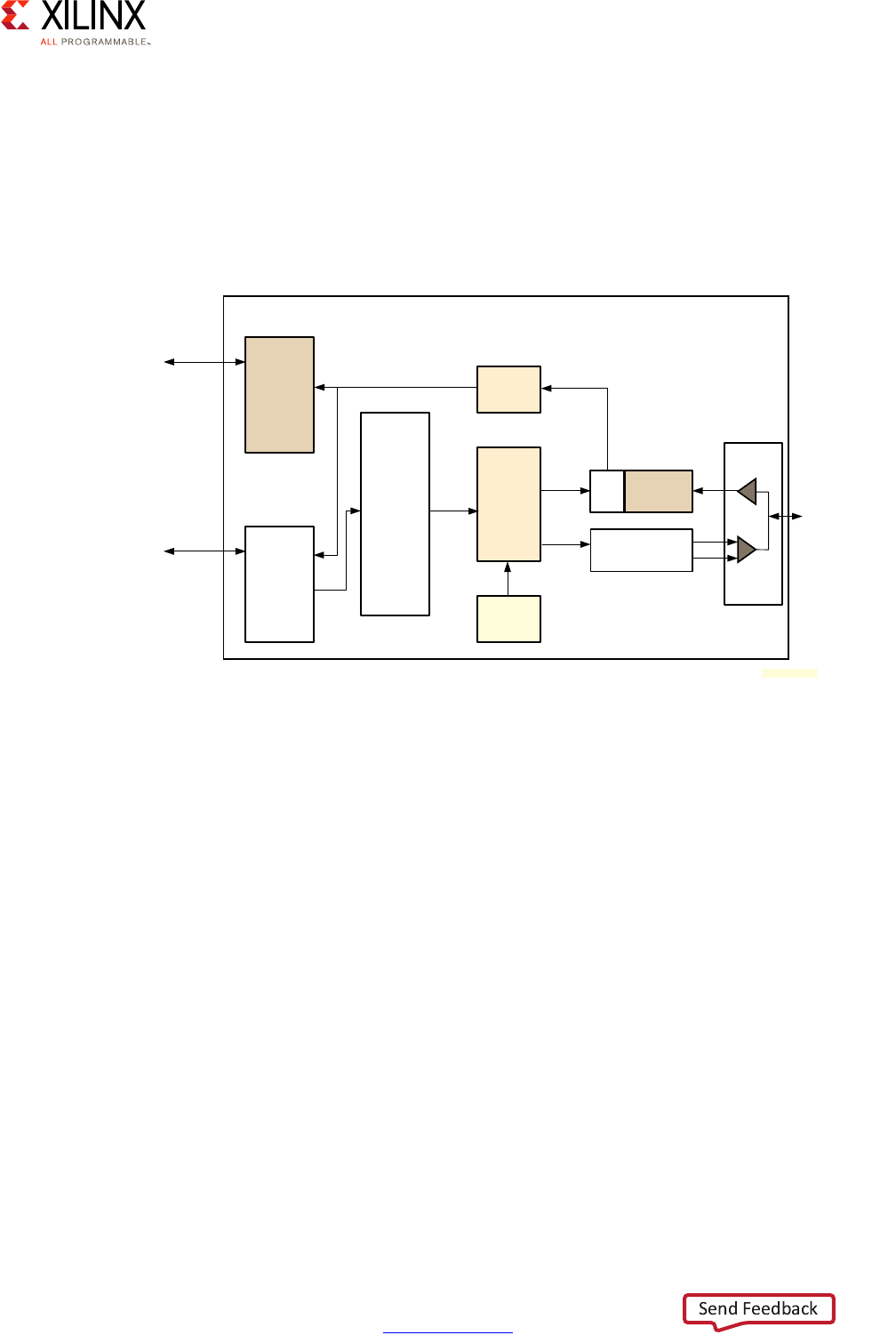
Zynq UltraScale+ MPSoC Embedded Design Methodology Guide 204
UG1228 (v1.0) March 31, 2017 www.xilinx.com
Chapter 10: Peripherals
Generic Quad-SPI Controller
The Generic Quad-SPI controller is a SPI controller with four data lines instead of one. To
reduce the number of wires, the communication is half duplex instead of full duplex like
simple SPI controllers. The Generic Quad-SPI controller supports all the features of the SPI
protocol. It exposes a command-based interface. The commands sent to the controller must
be written through register programming in the generic command FIFO, as illustrated in the
following figure.
Unlike the SPI controller, the Generic Quad-SPI controller contains both an AXI master and
an AXI slave since it supports DMA transfers as well as programmed IO.
DMA
The Generic Quad-SPI controller DMA does not use descriptors. Each DMA request needs to
be configured by programming the destination and size of the data to transfer in the
correct register in the controller.
I/O Mode
In this mode the clients read directly from the RXFIFO and TXFIFO buffers using registers.
Legacy Quad-SPI Controller
The legacy Quad-SPI controller can only work in a mode called Linear Addressing Mode. In
this mode, the flash memory connected to the controller acts like read-only memory with
an AXI interface. Write commands to the controller in legacy mode are acknowledged but
ignored.
X-Ref Target - Figure 10-14
Figure 10-14: Generic Quad-SPI Controller Block Diagram
AXI Master
Write I/F
RX Capture
and
Delay Line
I/O
Logic
DIN
OEN
Generic Quad-SPI Controller
DMA
(AXI Master)
AXI Slave I/F
APB
Registers
Generic
FIFO
20 x 32
RX
FIFO
Command
Generator
TX
FIFO
Quad
SPI
RX
Quad-SPI TX
DOUT
X18904-032017
Zynq UltraScale+ MPSoC Embedded Design Methodology Guide 205
UG1228 (v1.0) March 31, 2017 www.xilinx.com
Chapter 10: Peripherals
Flash Memory Arrangements
The Generic Quad-SPI controller can be linked in two different ways to two SPI flash
memories as illustrated in the following figure.
X-Ref Target - Figure 10-15
Figure 10-15: Stacked Mode | Dual Parallel Mode
Generic
Quad-SPI
Controller
SPI Flash
Memory Upper
SPI Flash
Memory Lower
QSPI1_SCLK
QSPI1_SS_B
QSPI1_IO[3:0]
QSPI0_SCLK
QSPI0_SS_B
QSPI0_IO[3:0]
Generic
Quad-SPI
Controller
SPI Flash
Memory Upper
SPI Flash
Memory Lower
QSPI0_SCLK
QSPI0_SS_B
QSPI0_IO[3:0]
QSPI1_SS_B
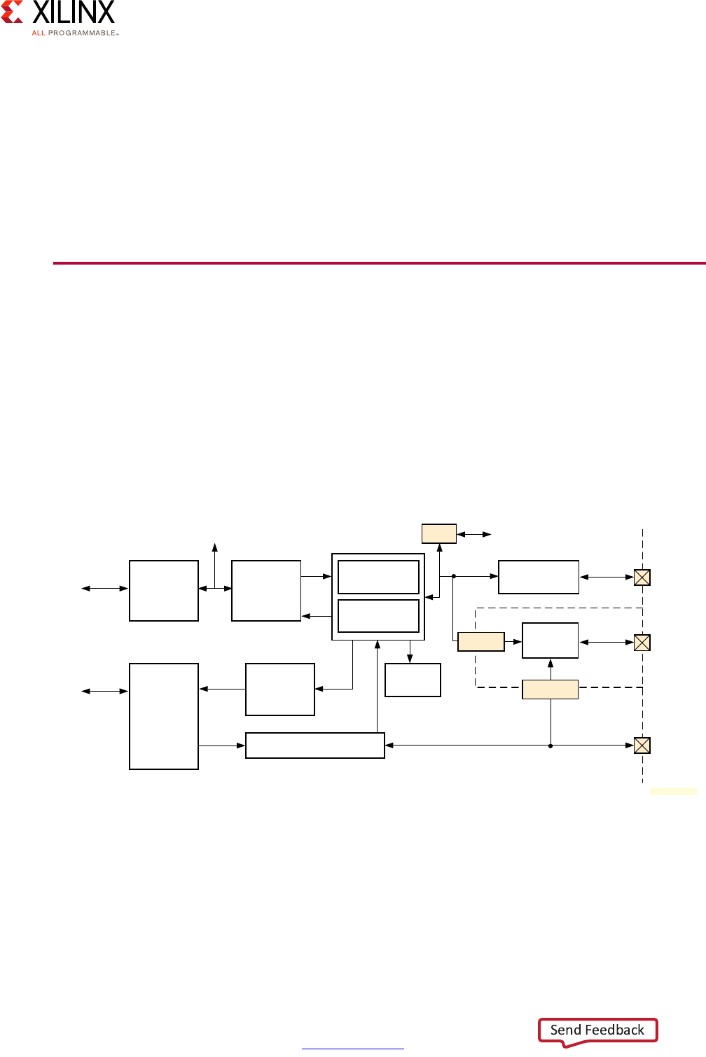
Zynq UltraScale+ MPSoC Embedded Design Methodology Guide 206
UG1228 (v1.0) March 31, 2017 www.xilinx.com
Chapter 10: Peripherals
In stacked mode the Chip Select signal can be used to access a specific memory between
the two. The controller can also be configured to split data between the two memories by
using the controller Stripe command. When the stripe feature is used, the bytes in even
positions are sent to the lower data bus and the other data bytes are sent in the upper data
bus.
The Legacy Quad-SPI controller also supports dual-parallel mode where a single data bus is
connected to both flash memories. The selection of one or the other memory is controlled
by the data bus select field.
Gigabit Ethernet Controller
The Zynq UltraScale+ device includes four Gigabit Ethernet Controllers implementing a
10/100/1000 Mb/s Ethernet MAC. The Ethernet controller supports several Media
Independent Interfaces, depending on how it is configured. Gigabit Media Independent
Interface (GMII) is used when the controller is routed through the PL pins using EMIO.
Reduced Gigabit Media Independent Interface (RGMII) is used when the controller is routed
through MIO. Serial Gigabit Media Independent Interface (SGMII) is used when the
controller is routed through the PS-GTR. The figure below provides the Ethernet controller
block diagram.
X-Ref Target - Figure 10-16
Figure 10-16: Ethernet Controller Block Diagram
PCS
DMA
Controller
AXI Master AXI
FIFO
Interface
MAC
Transmitter
MAC
Receiver
GMII to RGMII
Adapter
Register
Interface
APB Slave Status and
Statistics
Registers
Control Registers
GMII to RGMII
Adapter
RGMII
EMIO PL
User
Defined
Device
Boundary
MDC, MDIO
Frame
Filtering
GMII/MII
EMIO
MIO
Pins
PL
Signals
MIO
Pins
External FIFO interface Ten-bit Interface
(SGMII)
X18907-032017

Zynq UltraScale+ MPSoC Embedded Design Methodology Guide 207
UG1228 (v1.0) March 31, 2017 www.xilinx.com
Chapter 10: Peripherals
MAC Filtering
The Ethernet controller supports MAC filtering. The controller will compare received
packets with the configuration of a controller to see if they should be written to the FIFO for
DMA or PIO transfer.
Promiscuous Mode
When an Ethernet controller is set in promiscuous mode, all valid frames are copied to
memory.
Specific Addresses
A controller can be configured to filter based on up to four specific addresses. When such
a frame is received from one of those addresses, it is copied to the FIFO.
Broadcast Address
The controller can be configured to refuse or accept broadcast packets.
Pause Frames
Pause Frames are a feature of flow control defined in the IEEE 802.3x standard. The Zynq
UltraScale+ device Ethernet controllers can be configured to disable the copy of Pause
Frames.
VLAN support
The MPSoC Ethernet controllers can be configured to only receive packets destined to a
specific Virtual LAN (VLAN).
Wake-on-LAN
The receive block in the Ethernet controller supports wake-on-LAN (WOL) by detecting the
following events:
•Magic packets
• Address resolution protocol (ARP) requests to the device IP address
• Specific address 1 filter match
• Multicast hash filter match
On detection of any of the above events, the wake-up interrupt is triggered.
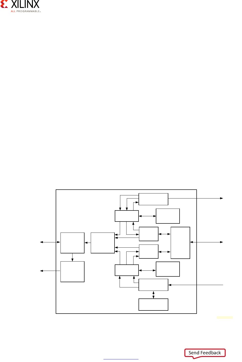
Zynq UltraScale+ MPSoC Embedded Design Methodology Guide 208
UG1228 (v1.0) March 31, 2017 www.xilinx.com
Chapter 10: Peripherals
Gigabit Ethernet DMA
The Ethernet controller supports Scatter/Gather DMA. The descriptors do not have a static
format and depend on the controller operating mode and depend on whether the buffer is
to be used to receive (RX) or transmit (TX) data. The descriptor size will vary between 64 and
196 bits depending on whether 64-bit addressing is enabled or if timestamp capture
(described below) is enabled in the controller.
The DMA descriptors precise structure is defined in the Zynq UltraScale+ MPSoC Technical
Reference Manual (UG1085) [Ref 7], but they include the following important fields:
• The memory address of the data to send
• Checksum offloading status
•VLAN tag and priority
Note: Refer to the Zynq UltraScale+ MPSoC Technical Reference Manual (UG1085) [Ref 7] for a full
list of parameters.
The Zynq UltraScale+ device Ethernet controller has packet buffers in both transmit and
receive paths thereby facilitating AXI DMA transfers. The DMA controller structure with the
packet buffers included is illustrated in the figure below. The packet buffer also enables full
support for checksum offloading given that complete packets are available in memory for
checking. Packet storage also enables the controller to automatically retry to send packets
on the wire when there are collisions.
X-Ref Target - Figure 10-17
Figure 10-17: DMA Packet Buffer
Register
Interface
APB
Interconnect
Control
Registers
MDIO
MIO or EMIO
Status and
Statistic
Registers
TX Packet
Buffer
RX Packet
Buffer
TX Packet
Buffer
DPSRAM
TX
DMA
RX
DMA
AXI
DMA
MAC
Transmitter
RX Packet
Buffer
DPSRAM
MAC
Receive
Frame
Filtering
Gigabit
Ethernet
Controller
AXI
Interconnect
TX GMII
MIO or EMIO
RX GMII
MIO or EMIO
X18908-032017

Zynq UltraScale+ MPSoC Embedded Design Methodology Guide 209
UG1228 (v1.0) March 31, 2017 www.xilinx.com
Chapter 10: Peripherals
Checksum Offloading
A Zynq UltraScale+ device Ethernet controller can be used to perform checksum offloading
in both TX and RX directions.
When receiving a packet and checksum offloading is enabled, the checksum headers of IPv4
packets, and TCP and UDP packets can be validated. The controller leaves a trace of the
checksum validation in the descriptor used to handle the reception. If the checksum is
invalid, the controller will discard the packet.
When sending a packet, the checksum of each packet stored in the packet buffer is
calculated based on automatic protocol detection of the frame being transmitted. The
checksum is calculated on UDP, TCP and IPv4 packets.
USB
The Zynq UltraScale+ device USB 3.0 controller consists of two independent dual role
device (DRD) controllers. The controller can expose xHCI functionality through the AXI slave
interface. The controller also offers a DMA interface which uses an AXI master interface to
transfer data.
The figure below is a high level view of the USB controller on the Zynq UltraScale+ device.
The AXI bus gives access to the USB controller Configuration Status Register (CSR) which
controls the mode that each USB DRD controller is set to.
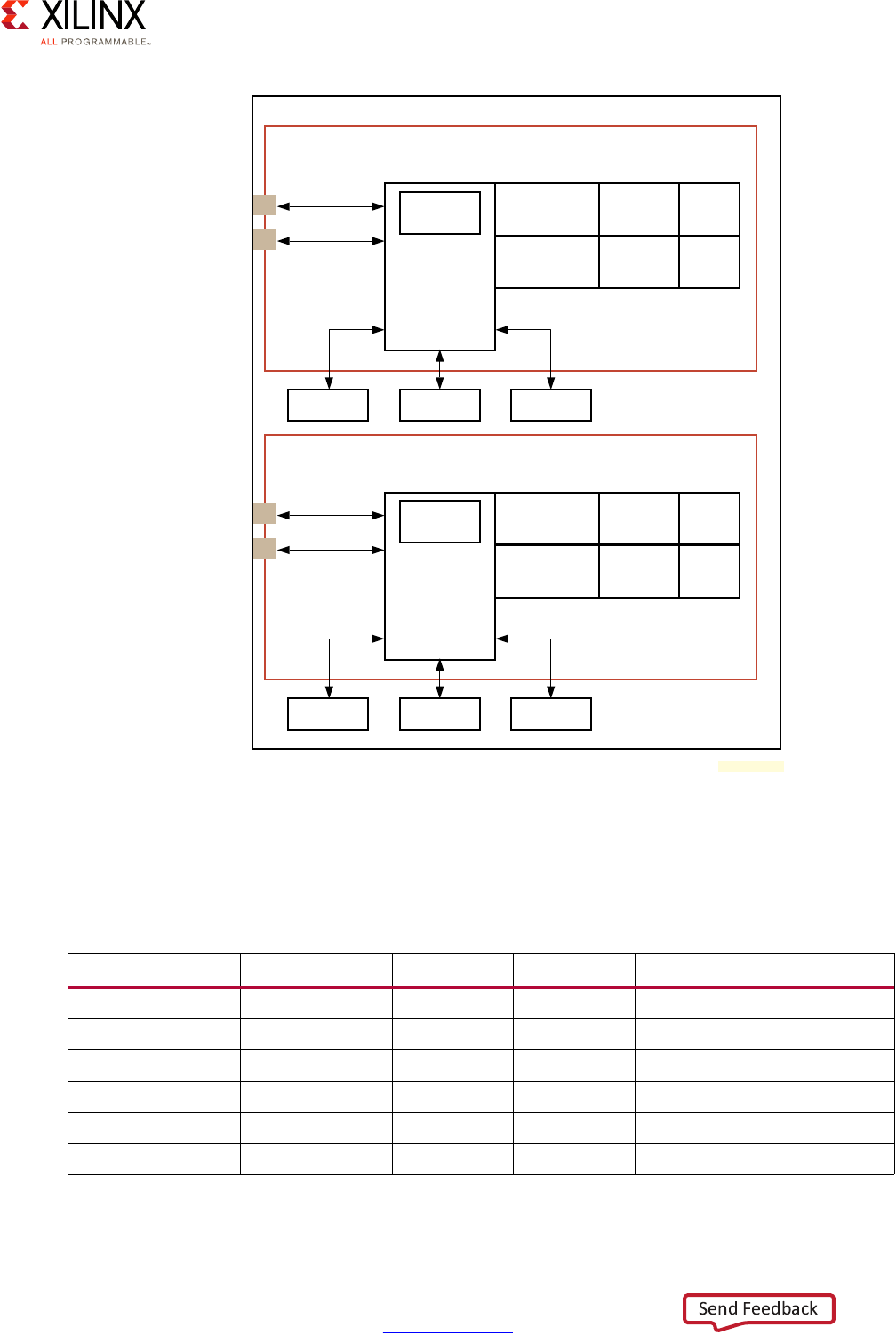
Zynq UltraScale+ MPSoC Embedded Design Methodology Guide 210
UG1228 (v1.0) March 31, 2017 www.xilinx.com
Chapter 10: Peripherals
Depending on the USB version that needs to be supported and whether the USB controllers
are connected through MIO or the PS-GTR, the standard USB protocol speeds listed in the
following table are supported.
X-Ref Target - Figure 10-18
Figure 10-18: Zynq UltraScale+ Device USB 3.0 Block Diagram
Table 10-1: USB 3.0 Controller Configuration
Configuration PHY Interface Super Speed High Speed Full Speed Low Speed
USB 2.0 host ULPI Yes Yes Yes
USB 2.0 device ULPI Yes Yes Yes
USB 2.0 OTG ULPI Yes Yes Yes
USB 3.0 host (xHCI) PIPE3 Yes Yes Yes Yes
USB 3.0 device PIPE3 Yes Yes Yes
USB 3.0 OTG IPIE3 Yes Yes Yes Yes (only Host)
USB 3.0 Dual Role Device Controller 1
AXI Bus
Interface,
Buffer, and
Register
Management
Module
CSR
Regs
USB 3 Protocol
Layer
USB 3 Link
Layer
PIPE3
Interface
USB 2 Protocol
Layer
USB 2 Link
Layer
ULPI
Interface
RAM1RAM0 RAM2
SCSR Access
MDMA
USB 3.0 Dual Role Device Controller 2
AXI Bus
Interface,
Buffer, and
Register
Management
Module
CSR
Regs
USB 3 Protocol
Layer
USB 3 Link
Layer
PIPE3
Interface
USB 2 Protocol
Layer
USB 2 Link
Layer
ULPI
Interface
RAM1RAM0 RAM2
SCSR Access
MDMA
To
AXI
Switch
To
AXI
Switch
Zynq UltraScale+ MPSoC USB 3.0 block
X18909-032017
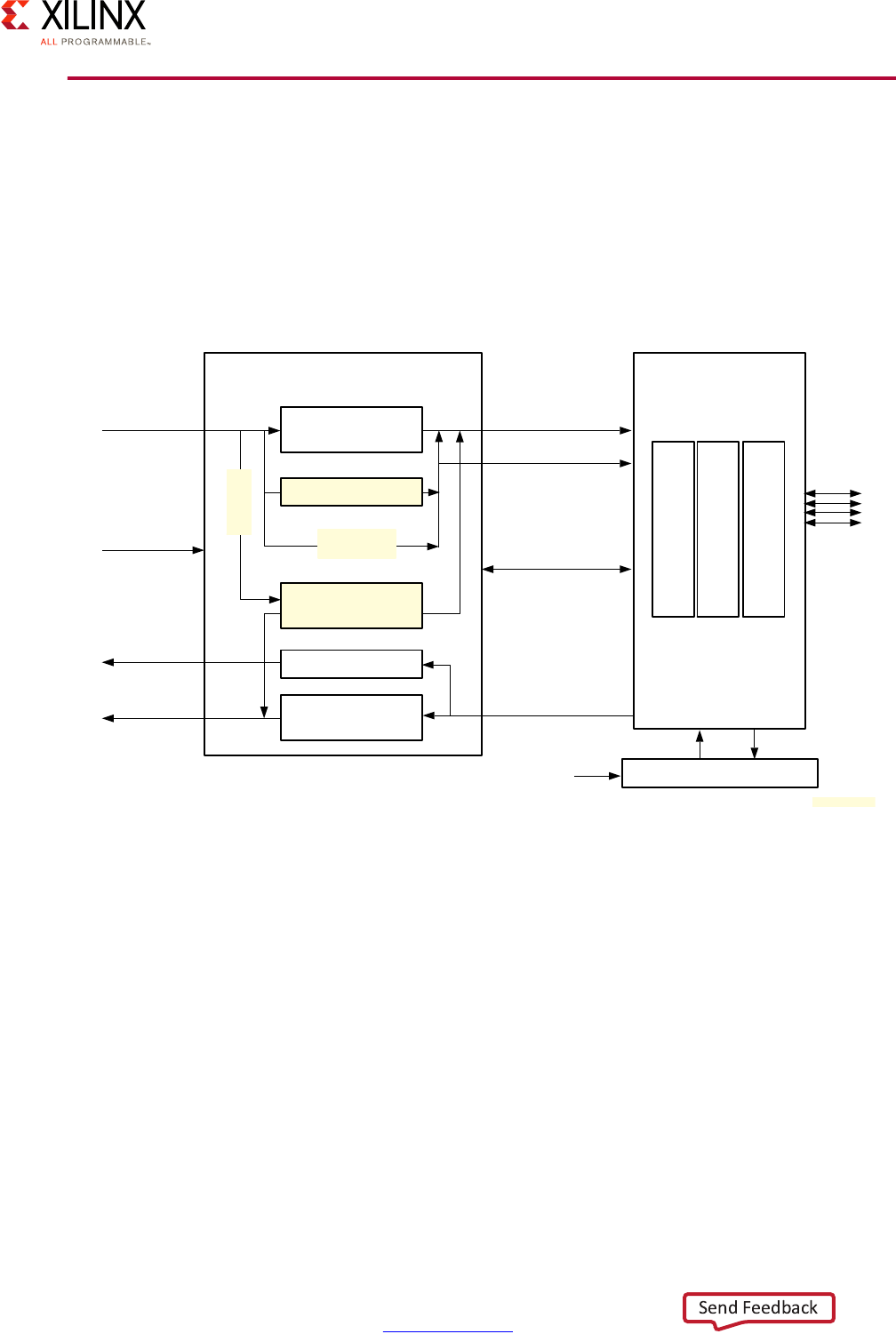
Zynq UltraScale+ MPSoC Embedded Design Methodology Guide 211
UG1228 (v1.0) March 31, 2017 www.xilinx.com
Chapter 10: Peripherals
PCI Express
The integrated block on the Zynq UltraScale+ device implements revision 2.1 of the PCI
Express Base Specification. The Zynq UltraScale+ device can act as a PCIe Endpoint as well
as a PCIe Root Port. A PCIe Root Port is a device that can host and communicate with other
PCIe devices while a PCIe Endpoint is a device able to act as a client to a Root Port. The
following figure illustrates the PCIe controller block diagram for the Zynq UltraScale+
device.
Given that PCIe is effectively a bus and that the internal interconnect of the Zynq
UltraScale+ device is AXI-based, one of the main components of the PCIe controller is an
AXI-PCIe bridge that interfaces the internal AXI interconnect to a block that manages the
PCIe Endpoints. This enables internal components to communicate with PCIe-connected
devices using AXI transactions.
Power Management
While the PCI Express Base Specification r2.1 indicates four possible power management
states, the PCIe controller in the Zynq UltraScale+ device supports two power management
levels only, L0 and L1. Also note that the controller does not support Active State Power
Manager (ASPM). Transitioning between L0 and L1 can be controlled manually through
Programmed Power Manager (PPM).
X-Ref Target - Figure 10-19
Figure 10-19: PCIe Controller Block Diagram
AXI-PCIe Bridge
(DMA, RP/EP)
Integrated Block for PCIe
Egress Address
Translation / BAR
MSI/INTx/Msg
Ingress Address
Translation/BAR
Transaction Layer
Data Link Layer
Physical Layer
Configuration/Status Register
AXI3 64-bit
Clock/Reset
Interrupts
AXI3 64-bit
AXI4 Streaming
AXI4 Streaming
Configuration Status
APB
PCIe Configuration
ECAM Write FIFO
DMA (4 channels)
Blk Reg
ECAM
Read Sidebands
(interrupts etc.)
PIPE
X18910-032017
Zynq UltraScale+ MPSoC Embedded Design Methodology Guide 212
UG1228 (v1.0) March 31, 2017 www.xilinx.com
Chapter 10: Peripherals
Security
The PCIe controller AXI masters is capable of generating transactions with TrustZone secure
and non-secure classification, as discussed in the Resource Isolation and Partitioning
Chapter. The classification of each address translation and each DMA channel can be
configured through register programming in the controller programming interface.
DMA
The Zynq UltraScale+ device PCIe controller supports a form of scatter gather DMA and
includes a 4 channel DMA engine. Each channel can be programmed for receive or transmit.
As shown in the figure below, PCIe DMA uses 3 different descriptor types for DMA.
SRC-SGL is the scatter-gather list of source data and DST-SGL corresponds to destination
data. The DMA engine also uses a list of descriptors that will hold the status of each source
and destination descriptor. Both use the same format defined as STAS/STAD-SGL in the
above figure. The DMA engine updates those descriptors on completion or in case of error
when the source data has been read in the case of SRC-SGL descriptors or when data has
been written at the destination in the case of DST-SGL.
Since the Zynq UltraScale+ device can act as an Endpoint, the DMA engine can be
configured to share the responsibility of the DMA functions with the host (i.e. Root Port) in
what is called Dual-CPU Control mode. In that case both the host CPU and an AXI CPU can
share control the DMA. The DMA can be configure to operate in Single CPU Control mode
where the host has full control over the DMA transfers.
X-Ref Target - Figure 10-20
Figure 10-20: DMA SGL-Q Format
Source Address [31:0]
Source Address [63:32]
Byte Count [23:0]
Flags [7:0]
UserHandle[15:0]
UserID[15:0]
SRC SGL Flags-
[0]: Location (AXI or PCIe)
[1]: EOP
[2]: Interrupt
[7:4]: Attributes
SRC-SGL
UserHandle[15:0]
UserID[15:0]
CMPLT
Error[3:1]
Completed Byte
Count [26:0]
Upper Status
Non-Zero
Error-
[1]: Source Error
[2]: Destination Error
[3]: Internal DMA Error
STAS/STAD-SGL
Destination Address [31:0]
Destination Address [63:32]
Byte Count [23:0]
Flags [7:0]
UserHandle[15:0]
UserID[15:0]
DST SGL Flags-
[0]: Location (AXI or PCIe)
[1]: Enable one packet per element
[7:4]: Attributes
DST-SGL
X18911-032017
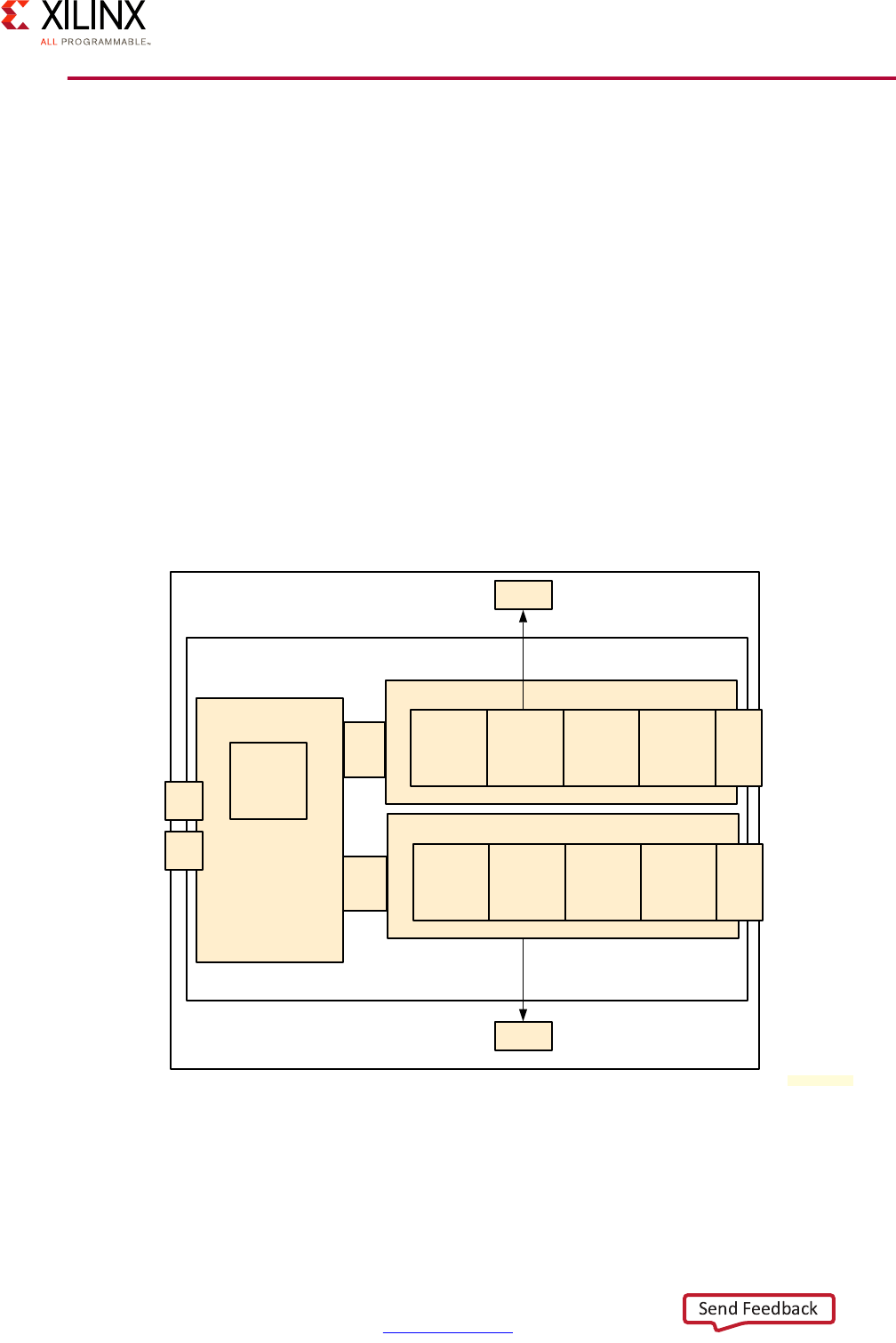
Zynq UltraScale+ MPSoC Embedded Design Methodology Guide 213
UG1228 (v1.0) March 31, 2017 www.xilinx.com
Chapter 10: Peripherals
SATA
The Serial ATA or SATA protocol was designed to replace the parallel ATA protocol (IDE)
used in early personal computers. The Zynq UltraScale+ device has two SATA controllers
supporting SATA generations from 1 to 3, and providing the following features:
• Compliant with AHCI v1.3
• Supports 1.5, 3.0, and 6.0 Gb/s data rates
• 64-bit AXI master port with a built-in DMA
Note: Refer to the Zynq UltraScale+ MPSoC Technical Reference Manual (UG1085) [Ref 7] for a full
list of parameters.
The block diagram from the Zynq UltraScale+ MPSoC device SATA controllers is illustrated
in the following figure. The Command Layer, Transport Layer, Link Layer, PHY Controller
Layer correspond to the corresponding layers as described in the SATA Host Controller
Interface Standard.
X-Ref Target - Figure 10-21
Figure 10-21: SATA System Block Diagram
Zynq UltraScale+MPSoC SATA Block
SATA Host Controller
DMA
AXI Engine
S
To
AXI
Switch
RAM
Port 0
Command
Layer
Transport
Layer Link Layer
PHY
Control
Layer
SerDes
Interface
AHCI
Regs
M
RAM
DMA
Port 1
Command
Layer
Transport
Layer Link Layer
PHY
Control
Layer
SerDes
Interface
To PS-GTR
MUX
To PS-GTR
MUX
X18912-032017
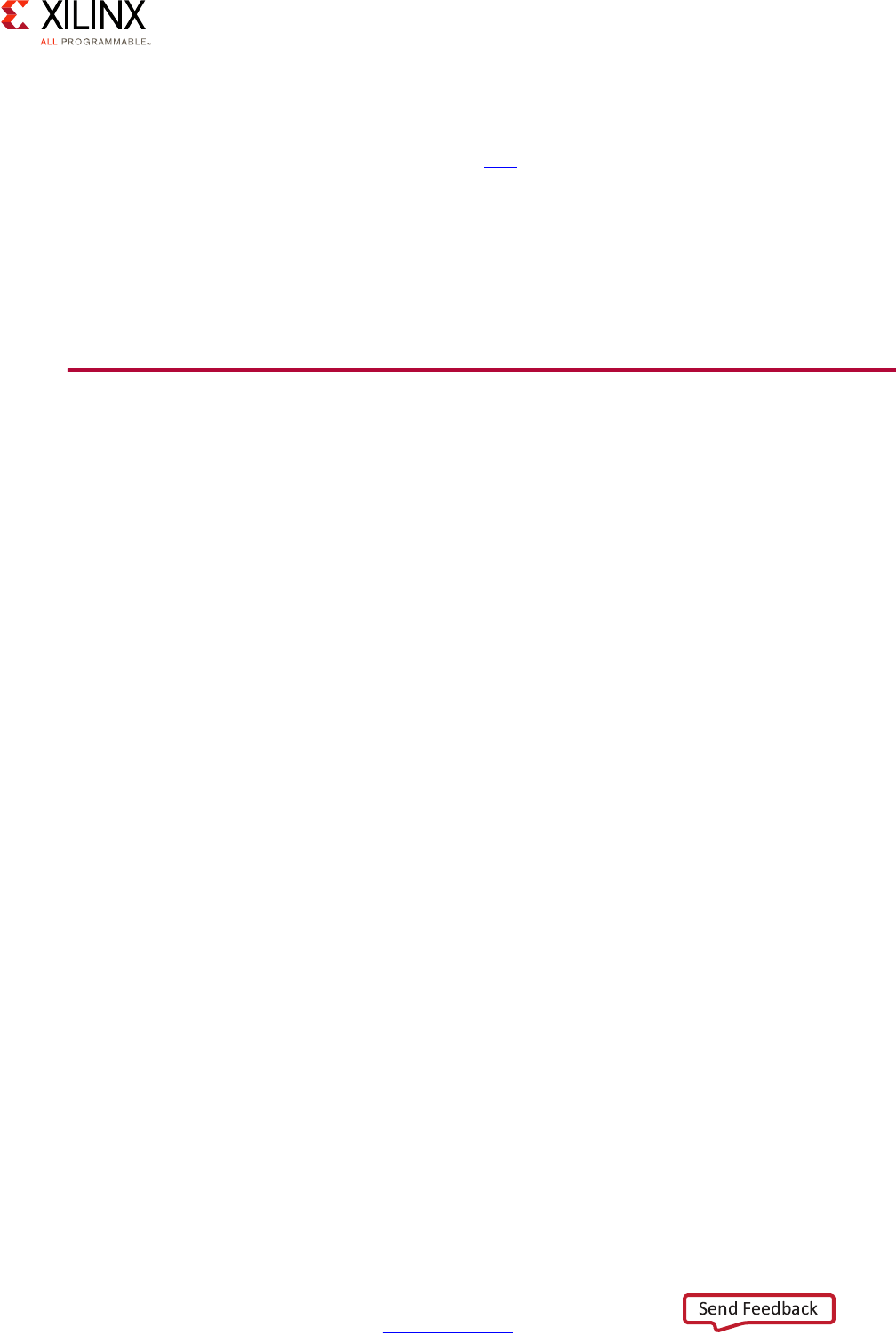
Zynq UltraScale+ MPSoC Embedded Design Methodology Guide 214
UG1228 (v1.0) March 31, 2017 www.xilinx.com
Chapter 10: Peripherals
SATA Security
The SATA controller is capable of enforcing TrustZone secure access on both its master and
slave port. The full details are provided at this link in the Zynq UltraScale+ MPSoC Technical
Reference Manual (UG1085) [Ref 7].
DMA
The DMA feature implemented in the Zynq UltraScale+ device SATA controller is based on
the DMA protocol defined in the Serial ATA Advanced Host Controller Interface (AHCI).
DisplayPort
The DisplayPort functionality of the Zynq UltraScale+ device is covered in Chapter 9,
Multimedia.
Zynq UltraScale+ MPSoC Embedded Design Methodology Guide 215
UG1228 (v1.0) March 31, 2017 www.xilinx.com
Appendix A
Additional Resources and Legal Notices
Xilinx Resources
For support resources such as Answers, Documentation, Downloads, and Forums, see Xilinx
Support.
Solution Centers
See the Xilinx Solution Centers for support on devices, software tools, and intellectual
property at all stages of the design cycle. Topics include design assistance, advisories, and
troubleshooting tips.
Documentation Navigator and Design Hubs
The Xilinx® Documentation Navigator provides access to Xilinx documents, videos, and
support resources, which you can filter and search to find information. To open the Xilinx®
Documentation Navigator (DocNav):
• From the Vivado® IDE, select Help > Documentation and Tutorials.
• On Windows, select Start > All Programs > Xilinx Design Tools > DocNav.
• At the Linux command prompt, enter docnav.
Xilinx Design Hubs provide links to documentation organized by design tasks and other
topics, which you can use to learn key concepts and address frequently asked questions. To
access the Design Hubs:
• In the Xilinx Documentation Navigator, click the Design Hubs View tab.
• On the Xilinx website, see the Design Hubs page.
Note: For more information on Documentation Navigator, see the Documentation Navigator page
on the Xilinx website.

Zynq UltraScale+ MPSoC Embedded Design Methodology Guide 216
UG1228 (v1.0) March 31, 2017 www.xilinx.com
Appendix A: Additional Resources and Legal Notices
References
1. Xilinx Power Estimator User Guide (UG440)
2. UltraScale Architecture Configuration User Guide (UG570)
3. Vivado Design Suite Tutorial: Partial Reconfiguration (UG947)
4. UltraFast Design Methodology Guide for the Vivado Design Suite (UG949)
5. Zynq UltraScale+ MPSoC: Software Developers Guide (UG1137)
6. Embedded Energy Management Interface Specification (UG1200)
7. Zynq UltraScale+ MPSoC Technical Reference Manual (UG1085)
8. Zynq UltraScale+ MPSoC OpenAMP: Getting Started Guide (UG1186)
9. SDSoC Environment Tutorial: Introduction (UG1028)
10. Xilinx White Paper: Unleash the Unparalleled Power and Flexibility of Zynq UltraScale+
MPSoCs (WP470)
11. Xilinx Software Development Kit (SDK) User Guide: System Performance Analysis
(UG1145)
12. Xilinx All Programmable Functional Safety Design Flow Solution Product Brief (PB015)
13. Xilinx Reduces Risk and Increases Efficiency for IEC61508 and ISO26262 Certified Safety
Applications White Paper (WP461)
14. Xilinx Software Development Kit web page:
https://www.xilinx.com/products/design-tools/embedded-software/sdk.html
15. Xilinx Vivado Design Suite web page:
https://www.xilinx.com/products/design-tools/vivado.html
16. Xilinx Isolation Design Flow web page:
https://www.xilinx.com/applications/isolation-design-flow.html.
17. Partial Reconfiguration web page:
https://www.xilinx.com/products/design-tools/vivado/implementation/partial-reconfig
uration.html
18. All Programmable Heterogeneous MPSoC web page:
https://www.xilinx.com/products/silicon-devices/soc/zynq-ultrascale-mpsoc.html#prod
uctTable
19. Zynq UltraScale+ MPSoC Graphics-GPU application debugging using ARM Mali Graphics
Debugger Tool Wiki page:
http://www.wiki.xilinx.com/Zynq+UltraScale%EF%BC%8BMPSoC+Graphics-+GPU+appli
cation+debugging+using+ARM+Mali+Graphics+Debugger+tool
Zynq UltraScale+ MPSoC Embedded Design Methodology Guide 217
UG1228 (v1.0) March 31, 2017 www.xilinx.com
Appendix A: Additional Resources and Legal Notices
Please Read: Important Legal Notices
The information disclosed to you hereunder (the “Materials”) is provided solely for the selection and use of Xilinx products. To the
maximum extent permitted by applicable law: (1) Materials are made available "AS IS" and with all faults, Xilinx hereby DISCLAIMS
ALL WARRANTIES AND CONDITIONS, EXPRESS, IMPLIED, OR STATUTORY, INCLUDING BUT NOT LIMITED TO WARRANTIES OF
MERCHANTABILITY, NON-INFRINGEMENT, OR FITNESS FOR ANY PARTICULAR PURPOSE; and (2) Xilinx shall not be liable (whether
in contract or tort, including negligence, or under any other theory of liability) for any loss or damage of any kind or nature related
to, arising under, or in connection with, the Materials (including your use of the Materials), including for any direct, indirect, special,
incidental, or consequential loss or damage (including loss of data, profits, goodwill, or any type of loss or damage suffered as a
result of any action brought by a third party) even if such damage or loss was reasonably foreseeable or Xilinx had been advised
of the possibility of the same. Xilinx assumes no obligation to correct any errors contained in the Materials or to notify you of
updates to the Materials or to product specifications. You may not reproduce, modify, distribute, or publicly display the Materials
without prior written consent. Certain products are subject to the terms and conditions of Xilinx’s limited warranty, please refer to
Xilinx’s Terms of Sale which can be viewed at http://www.xilinx.com/legal.htm#tos; IP cores may be subject to warranty and support
terms contained in a license issued to you by Xilinx. Xilinx products are not designed or intended to be fail-safe or for use in any
application requiring fail-safe performance; you assume sole risk and liability for use of Xilinx products in such critical applications,
please refer to Xilinx’s Terms of Sale which can be viewed at http://www.xilinx.com/legal.htm#tos.
AUTOMOTIVE APPLICATIONS DISCLAIMER
AUTOMOTIVE PRODUCTS (IDENTIFIED AS "XA" IN THE PART NUMBER) ARE NOT WARRANTED FOR USE IN THE DEPLOYMENT OF
AIRBAGS OR FOR USE IN APPLICATIONS THAT AFFECT CONTROL OF A VEHICLE ("SAFETY APPLICATION") UNLESS THERE IS A
SAFETY CONCEPT OR REDUNDANCY FEATURE CONSISTENT WITH THE ISO 26262 AUTOMOTIVE SAFETY STANDARD ("SAFETY
DESIGN"). CUSTOMER SHALL, PRIOR TO USING OR DISTRIBUTING ANY SYSTEMS THAT INCORPORATE PRODUCTS, THOROUGHLY
TEST SUCH SYSTEMS FOR SAFETY PURPOSES. USE OF PRODUCTS IN A SAFETY APPLICATION WITHOUT A SAFETY DESIGN IS FULLY
AT THE RISK OF CUSTOMER, SUBJECT ONLY TO APPLICABLE LAWS AND REGULATIONS GOVERNING LIMITATIONS ON PRODUCT
LIABILITY.
© Copyright 2017 Xilinx, Inc. Xilinx, the Xilinx logo, Artix, ISE, Kintex, Spartan, Virtex, Vivado, Zynq, and other designated brands
included herein are trademarks of Xilinx in the United States and other countries. All other trademarks are the property of their
respective owners.
