Spartan 6 FPGA SelectIO Resources User Guide (UG381) Ug381 Select IO
User Manual:
Open the PDF directly: View PDF ![]() .
.
Page Count: 98
- Spartan-6 FPGA SelectIO Resources
- Revision History
- Table of Contents
- About This Guide
- SelectIO Resources
- SelectIO Logic Resources
- Advanced SelectIO Logic Resources

Spartan-6 FPGA
SelectIO Resources
User Guide
UG381 (v1.7) October 21, 2015
Spartan-6 FPGA SelectIO Resources www.xilinx.com UG381 (v1.7) October 21, 2015
Notice of Disclaimer
The information disclosed to you hereunder (the “Materials”) is provided solely for the selection and use of Xilinx products. To the maximum
extent permitted by applicable law: (1) Materials are made available "AS IS" and with all faults, Xilinx hereby DISCLAIMS ALL
WARRANTIES AND CONDITIONS, EXPRESS, IMPLIED, OR STATUTORY, INCLUDING BUT NOT LIMITED TO WARRANTIES OF
MERCHANTABILITY, NON-INFRINGEMENT, OR FITNESS FOR ANY PARTICULAR PURPOSE; and (2) Xilinx shall not be liable (whether
in contract or tort, including negligence, or under any other theory of liability) for any loss or damage of any kind or nature related to, arising
under, or in connection with, the Materials (including your use of the Materials), including for any direct, indirect, special, incidental, or
consequential loss or damage (including loss of data, profits, goodwill, or any type of loss or damage suffered as a result of any action
brought by a third party) even if such damage or loss was reasonably foreseeable or Xilinx had been advised of the possibility of the same.
Xilinx assumes no obligation to correct any errors contained in the Materials or to notify you of updates to the Materials or to product
specifications. You may not reproduce, modify, distribute, or publicly display the Materials without prior written consent. Certain products are
subject to the terms and conditions of Xilinx’s limited warranty, please refer to Xilinx’s Terms of Sale which can be viewed at
www.xilinx.com/legal.htm#tos; IP cores may be subject to warranty and support terms contained in a license issued to you by Xilinx. Xilinx
products are not designed or intended to be fail-safe or for use in any application requiring fail-safe performance; you assume sole risk and
liability for use of Xilinx products in such critical applications, please refer to Xilinx’s Terms of Sale which can be viewed at
www.xilinx.com/legal.htm#tos.
Automotive Applications Disclaimer
XILINX PRODUCTS ARE NOT DESIGNED OR INTENDED TO BE FAIL-SAFE, OR FOR USE IN ANY APPLICATION REQUIRING FAIL-
SAFE PERFORMANCE, SUCH AS APPLICATIONS RELATED TO: (I) THE DEPLOYMENT OF AIRBAGS, (II) CONTROL OF A VEHICLE,
UNLESS THERE IS A FAIL-SAFE OR REDUNDANCY FEATURE (WHICH DOES NOT INCLUDE USE OF SOFTWARE IN THE XILINX
DEVICE TO IMPLEMENT THE REDUNDANCY) AND A WARNING SIGNAL UPON FAILURE TO THE OPERATOR, OR (III) USES THAT
COULD LEAD TO DEATH OR PERSONAL INJURY. CUSTOMER ASSUMES THE SOLE RISK AND LIABILITY OF ANY USE OF XILINX
PRODUCTS IN SUCH APPLICATIONS.
© Copyright 2009—2015 Xilinx, Inc. Xilinx, the Xilinx logo, Artix, ISE, Kintex, Spartan, Virtex, Vivado, Zynq, and other designated brands
included herein are trademarks of Xilinx in the United States and other countries. All other trademarks are the property of their respective
owners.
Revision History
The following table shows the revision history for this document.
Date Version Revision
06/24/2009 1.0 Initial Xilinx release.
01/05/2010 1.1 Updated On-Chip Termination Benefits. Added PCI66_3 to Table 1-5. Revised
Figure 1-6. Clarifying text edits on pages 16, 17, and 18. Added IBUFDS_DIFF_OUT
and IBUFGDS_DIFF_OUT to the Spartan-6 FPGA SelectIO Primitives section
including updating Figure 1-13. Clarified bank availability of LVDS_25, LVDS_33,
Mini-LVDS, RSDS, TMDS, and PPDS on page 28 and 29. Clarified the title of Figure 1-19
and added Figure 1-20. Added 2.5V VCCO to Figure 1-19 and TMDS_33. Updated
Figure 1-20. Revised Figure 1-22. Moved the section HSTL/SSTL VREF Reference
Voltage. Removed the section Voltage Clamps Using Internal Diodes Enabled By Using PCI
I/O Standards.
Changed SYNC and SRTYPE description in Table 2-2. Corrected Figure 2-5 by switching
C0 and C1 inputs. Added a clarifying note to Output DDR Overview (ODDR2). Updated
the discussion around Figure 2-20. Updated discussion in I/O Delay Calibration and
Reset.
Changed description of DATA_RATE. Updated discussion in Cascade Operation.
Updated Phase Detector Overview. Updated MASTER ISERDES2 in Figure 3-5, page 85.
Clarifying sample timing on page 88. Changed descriptions of attributes in Table 3-6.
Updated discussion in Cascade Operation. Redrew Figure 3-13, page 96.

UG381 (v1.7) October 21, 2015 www.xilinx.com Spartan-6 FPGA SelectIO Resources
02/02/2010 1.2 Removed the invalid M2 mode from I/O Pins During Power-On and Configuration in
Chapter 1. Removed Figures 1-19 though 1-28. Updated Table 1-5 with bank restrictions
discussion.
Updated Figure 2-1. Added Clock Resources Available to the I/O Interface Logic
including Figure 2-2 and Table 2-1.
Revised SerDes ratios in the ISERDES2 Overview and OSERDES2 Overview
introductions. Updated Phase Detector Overview introduction. Revised Figure 3-5.
Added further clarification to OSERDES2 Operation. Added Table 3-7 and updated
Figure 3-11.
03/15/2010 1.3 Revised Table 1-5, see DS162: Spartan-6 FPGA Data Sheet for recommended operating
conditions. Added Pin-Planning to Mitigate SSO Sensitivity section.
Updated Figure 2-1. Clarified I/O Delay Overview and I/O Delay Modes. Updated INC
in Figure 2-21 and Table 2-8.
Updated CE0, BITSLIP, and IOCE descriptions in Table 3-1. Modified Figure 3-1 and
Figure 3-11 to include a flip-flop on the I/O clock-enable line. Updated IOCE in
Table 3-5. Updated OUTPUT_MODE in Table 3-6.
12/16/2010 1.4 Updated I/O Termination Techniques to include both series and differential termination
which includes an update to Figure 1-18 and the addition of Table 1-3. Corrected the
VCCO for DISPLAY_PORT in Table 1-6. Clarified discussion of I/O Pins During Power-
On and Configuration.
Clarified the discussions in I/O Interface Tile, page 48 and Clock Resources Available to
the I/O Interface Logic, page 49. In Table 2-1, revised the SDR BUFPLL Clock
description. In Table 2-2 and Table 2-5, revised the descriptions of C0. In Table 2-3 and
Table 2-6, updated DDR_ALIGNMENT descriptions. Updated Figure 2-5, Figure 2-7,
Figure 2-11, and added Figure 2-12 and Figure 2-13. Revised Figure 2-15 and Figure 2-18.
Updated the I/O Delay Overview discussion. Updated Calibration Example. Clarified
the Delay Update and BUSY Timing section including adding Figure 2-22. In Table 2-8,
updated DATAOUT2 description. In Table 2-9, updated IDELAY_MODE and
IDELAY_TYPE and added DATA_RATE.
In Table 3-1, updated CLKDIV and BITSLIP descriptions. In Table 3-2, updated the
BITSLIP_ENABLE description. Revised Figure 3-1 and Figure 3-2. Revised example
code on page 84. Updated RETIMED Mode discussion. Revised Phase Detector
Calibration Mechanisms and Phase Detector Operation discussions including updating
Figure 3-6, Figure 3-7, Figure 3-8, and Figure 3-10. Updated CLKDIV in Table 3-5.
Clarified OCE/TCE in Figure 3-11.
02/07/2013 1.5 Updated I/O Delay Modes, I/O Delay Calibration and Reset, ISERDES2 Overview,
NETWORKING_PIPELINED Mode, and Bitslip Operation. Added CLKDIV and RST to
Figure 3-1.
02/14/2014 1.6 Updated disclaimer and copyright. Updated I2C—Inter-Integrated Circuit Bus, Pin-
Planning to Mitigate SSO Sensitivity, I/O Delay Modes, and OSERDES2 Overview.
Added Driving Unpowered I/O Banks. Updated Figure 1-19 and Table 2-9. Split
ISERDES2 Timing Diagram into Figure 3-2 and Figure 3-3 to show SDR and DDR
operation. Clarified SerDes ratios in OSERDES2 Overview.
10/21/2015 1.7 Updated ILOGIC2 Resources and Table 2-3.
Date Version Revision


Spartan-6 FPGA SelectIO Resources www.xilinx.com 5
UG381 (v1.7) October 21, 2015
Revision History . . . . . . . . . . . . . . . . . . . . . . . . . . . . . . . . . . . . . . . . . . . . . . . . . . . . . . . . . . . . . 2
Preface: About This Guide
Additional Documentation . . . . . . . . . . . . . . . . . . . . . . . . . . . . . . . . . . . . . . . . . . . . . . . . . . . 9
Additional Support Resources. . . . . . . . . . . . . . . . . . . . . . . . . . . . . . . . . . . . . . . . . . . . . . . 10
Chapter 1: SelectIO Resources
I/O Tile Overview. . . . . . . . . . . . . . . . . . . . . . . . . . . . . . . . . . . . . . . . . . . . . . . . . . . . . . . . . . . 11
SelectIO Resources Introduction . . . . . . . . . . . . . . . . . . . . . . . . . . . . . . . . . . . . . . . . . . . . 12
SelectIO Resources General Guidelines . . . . . . . . . . . . . . . . . . . . . . . . . . . . . . . . . . . . . 13
Spartan-6 FPGA SelectIO Banks . . . . . . . . . . . . . . . . . . . . . . . . . . . . . . . . . . . . . . . . . . . . 13
Output Drive Source Voltage (VCCO) Pins . . . . . . . . . . . . . . . . . . . . . . . . . . . . . . . . . . . 13
Internal Termination . . . . . . . . . . . . . . . . . . . . . . . . . . . . . . . . . . . . . . . . . . . . . . . . . . . . . . . . 14
Differential Termination . . . . . . . . . . . . . . . . . . . . . . . . . . . . . . . . . . . . . . . . . . . . . . . . . . . 14
Differential Termination Benefits . . . . . . . . . . . . . . . . . . . . . . . . . . . . . . . . . . . . . . . . . . 14
On-Chip Termination . . . . . . . . . . . . . . . . . . . . . . . . . . . . . . . . . . . . . . . . . . . . . . . . . . . . . 15
On-Chip Termination Benefits . . . . . . . . . . . . . . . . . . . . . . . . . . . . . . . . . . . . . . . . . . . . 15
Programmable Output Driver Impedance (Source Termination) . . . . . . . . . . . . . . . . . . 16
Programmable Input Termination Resistors (Split Termination) . . . . . . . . . . . . . . . . . . 17
Spartan-6 FPGA SelectIO Primitives. . . . . . . . . . . . . . . . . . . . . . . . . . . . . . . . . . . . . . . . . 18
IBUF and IBUFG . . . . . . . . . . . . . . . . . . . . . . . . . . . . . . . . . . . . . . . . . . . . . . . . . . . . . . . . . 18
OBUF . . . . . . . . . . . . . . . . . . . . . . . . . . . . . . . . . . . . . . . . . . . . . . . . . . . . . . . . . . . . . . . . . . . 19
OBUFT . . . . . . . . . . . . . . . . . . . . . . . . . . . . . . . . . . . . . . . . . . . . . . . . . . . . . . . . . . . . . . . . . . 19
IOBUF . . . . . . . . . . . . . . . . . . . . . . . . . . . . . . . . . . . . . . . . . . . . . . . . . . . . . . . . . . . . . . . . . . 19
IBUFDS and IBUFGDS . . . . . . . . . . . . . . . . . . . . . . . . . . . . . . . . . . . . . . . . . . . . . . . . . . . . 20
IBUFDS_DIFF_OUT and IBUFGDS_DIFF_OUT . . . . . . . . . . . . . . . . . . . . . . . . . . . . . . . 20
OBUFDS . . . . . . . . . . . . . . . . . . . . . . . . . . . . . . . . . . . . . . . . . . . . . . . . . . . . . . . . . . . . . . . . 20
OBUFTDS . . . . . . . . . . . . . . . . . . . . . . . . . . . . . . . . . . . . . . . . . . . . . . . . . . . . . . . . . . . . . . . 21
IOBUFDS . . . . . . . . . . . . . . . . . . . . . . . . . . . . . . . . . . . . . . . . . . . . . . . . . . . . . . . . . . . . . . . . 21
Spartan-6 FPGA SelectIO Attributes/Constraints . . . . . . . . . . . . . . . . . . . . . . . . . . . . . 21
Location Constraint . . . . . . . . . . . . . . . . . . . . . . . . . . . . . . . . . . . . . . . . . . . . . . . . . . . . 22
IOSTANDARD Attribute . . . . . . . . . . . . . . . . . . . . . . . . . . . . . . . . . . . . . . . . . . . . . . . . 22
Output Slew Rate Attribute . . . . . . . . . . . . . . . . . . . . . . . . . . . . . . . . . . . . . . . . . . . . . . 22
Output Drive Strength Attribute . . . . . . . . . . . . . . . . . . . . . . . . . . . . . . . . . . . . . . . . . . 23
PULLUP/PULLDOWN/KEEPER for IBUF, OBUFT, and IOBUF . . . . . . . . . . . . . . . . . 23
Differential Termination Attribute . . . . . . . . . . . . . . . . . . . . . . . . . . . . . . . . . . . . . . . . . 23
Input and Output Termination . . . . . . . . . . . . . . . . . . . . . . . . . . . . . . . . . . . . . . . . . . . . 24
SelectIO Signal Standards. . . . . . . . . . . . . . . . . . . . . . . . . . . . . . . . . . . . . . . . . . . . . . . . . . . 24
Overview of I/O Standards . . . . . . . . . . . . . . . . . . . . . . . . . . . . . . . . . . . . . . . . . . . . . . . . 24
LVTTL—Low-Voltage TTL. . . . . . . . . . . . . . . . . . . . . . . . . . . . . . . . . . . . . . . . . . . . . . . 26
LVCMOS—Low-Voltage CMOS. . . . . . . . . . . . . . . . . . . . . . . . . . . . . . . . . . . . . . . . . . . 26
LVCMOS_JEDEC—Low-Voltage CMOS with JEDEC Compliant Inputs. . . . . . . . . . . . 26
PCI—Peripheral Component Interface . . . . . . . . . . . . . . . . . . . . . . . . . . . . . . . . . . . . . . 26
I2C—Inter-Integrated Circuit Bus. . . . . . . . . . . . . . . . . . . . . . . . . . . . . . . . . . . . . . . . . . 26
SMBUS—System Management Bus . . . . . . . . . . . . . . . . . . . . . . . . . . . . . . . . . . . . . . . . 27
Table of Contents

6www.xilinx.com Spartan-6 FPGA SelectIO Resources
UG381 (v1.7) October 21, 2015
SDIO—SD Memory Card Interface. . . . . . . . . . . . . . . . . . . . . . . . . . . . . . . . . . . . . . . . . 27
MOBILE_DDR—Low Power DDR . . . . . . . . . . . . . . . . . . . . . . . . . . . . . . . . . . . . . . . . . 27
HSTL—High-Speed Transceiver Logic. . . . . . . . . . . . . . . . . . . . . . . . . . . . . . . . . . . . . . 27
SSTL3—Stub Series Terminated Logic for 3.3V . . . . . . . . . . . . . . . . . . . . . . . . . . . . . . . 27
SSTL2—Stub Series Terminated Logic for 2.5V . . . . . . . . . . . . . . . . . . . . . . . . . . . . . . . 27
SSTL18—Stub Series Terminated Logic for 1.8V. . . . . . . . . . . . . . . . . . . . . . . . . . . . . . . 27
SSTL15—Stub Series Terminated Logic for 1.5V. . . . . . . . . . . . . . . . . . . . . . . . . . . . . . . 28
LVDS_25—Low Voltage Differential Signal . . . . . . . . . . . . . . . . . . . . . . . . . . . . . . . . . . 28
LVDS_33—Low Voltage Differential Signal . . . . . . . . . . . . . . . . . . . . . . . . . . . . . . . . . . 28
BLVDS—Bus LVDS. . . . . . . . . . . . . . . . . . . . . . . . . . . . . . . . . . . . . . . . . . . . . . . . . . . . . 28
DISPLAY_PORT—AUX CH for DisplayPort . . . . . . . . . . . . . . . . . . . . . . . . . . . . . . . . . 28
Mini-LVDS . . . . . . . . . . . . . . . . . . . . . . . . . . . . . . . . . . . . . . . . . . . . . . . . . . . . . . . . . . . 29
RSDS—Reduced Swing Differential Signaling . . . . . . . . . . . . . . . . . . . . . . . . . . . . . . . . 29
TMDS—Transition Minimized Differential Signaling . . . . . . . . . . . . . . . . . . . . . . . . . . 29
PPDS—Point-to-Point Differential Signaling . . . . . . . . . . . . . . . . . . . . . . . . . . . . . . . . . 29
I/O Timing Analysis . . . . . . . . . . . . . . . . . . . . . . . . . . . . . . . . . . . . . . . . . . . . . . . . . . . . . . 29
Using IBIS Models to Simulate Load Conditions . . . . . . . . . . . . . . . . . . . . . . . . . . . . . . 30
LVCMOS/LVTTL Slew Rate Control and Drive Strength . . . . . . . . . . . . . . . . . . . . . . 30
Simultaneously Switching Outputs. . . . . . . . . . . . . . . . . . . . . . . . . . . . . . . . . . . . . . . . . . 31
Pin-Planning to Mitigate SSO Sensitivity . . . . . . . . . . . . . . . . . . . . . . . . . . . . . . . . . . . . 32
I/O Termination Techniques . . . . . . . . . . . . . . . . . . . . . . . . . . . . . . . . . . . . . . . . . . . . . . . 33
Differential I/O Standards . . . . . . . . . . . . . . . . . . . . . . . . . . . . . . . . . . . . . . . . . . . . . . . . . 36
TMDS_33 Termination . . . . . . . . . . . . . . . . . . . . . . . . . . . . . . . . . . . . . . . . . . . . . . . . . . 36
BLVDS Output Termination . . . . . . . . . . . . . . . . . . . . . . . . . . . . . . . . . . . . . . . . . . . . . . 36
Supply Voltages for the IOBs. . . . . . . . . . . . . . . . . . . . . . . . . . . . . . . . . . . . . . . . . . . . . . . . 37
HSTL/SSTL VREF Reference Voltage . . . . . . . . . . . . . . . . . . . . . . . . . . . . . . . . . . . . . . . . 37
ESD Protection . . . . . . . . . . . . . . . . . . . . . . . . . . . . . . . . . . . . . . . . . . . . . . . . . . . . . . . . . . . 38
I/O Standard Bank Compatibility . . . . . . . . . . . . . . . . . . . . . . . . . . . . . . . . . . . . . . . . . . . 38
Single-Ended I/O Compatibility . . . . . . . . . . . . . . . . . . . . . . . . . . . . . . . . . . . . . . . . . . 39
Differential I/O Standard Bank Compatibility . . . . . . . . . . . . . . . . . . . . . . . . . . . . . . . . 41
I/O Banking Rules . . . . . . . . . . . . . . . . . . . . . . . . . . . . . . . . . . . . . . . . . . . . . . . . . . . . . . . . 42
Using Large-Swing Signals . . . . . . . . . . . . . . . . . . . . . . . . . . . . . . . . . . . . . . . . . . . . . . . . . 44
Voltage Translators. . . . . . . . . . . . . . . . . . . . . . . . . . . . . . . . . . . . . . . . . . . . . . . . . . . . . 44
Open-Drain Interfacing. . . . . . . . . . . . . . . . . . . . . . . . . . . . . . . . . . . . . . . . . . . . . . . . . . 44
I/O Pins During Power-On and Configuration . . . . . . . . . . . . . . . . . . . . . . . . . . . . . . . 45
Unused I/O Pins After Configuration . . . . . . . . . . . . . . . . . . . . . . . . . . . . . . . . . . . . . . . 45
Driving Unpowered I/O Banks . . . . . . . . . . . . . . . . . . . . . . . . . . . . . . . . . . . . . . . . . . . . . 46
Chapter 2: SelectIO Logic Resources
Introduction . . . . . . . . . . . . . . . . . . . . . . . . . . . . . . . . . . . . . . . . . . . . . . . . . . . . . . . . . . . . . . . . 47
I/O Interface Tile. . . . . . . . . . . . . . . . . . . . . . . . . . . . . . . . . . . . . . . . . . . . . . . . . . . . . . . . . . . . 48
Clock Resources Available to the I/O Interface Logic. . . . . . . . . . . . . . . . . . . . . . . . . 49
ILOGIC2 Resources . . . . . . . . . . . . . . . . . . . . . . . . . . . . . . . . . . . . . . . . . . . . . . . . . . . . . . . . . 52
Combinatorial Input Path . . . . . . . . . . . . . . . . . . . . . . . . . . . . . . . . . . . . . . . . . . . . . . . . . . 53
Input DDR Primitive . . . . . . . . . . . . . . . . . . . . . . . . . . . . . . . . . . . . . . . . . . . . . . . . . . . . . . 53
IDDR2 VHDL and Verilog Templates . . . . . . . . . . . . . . . . . . . . . . . . . . . . . . . . . . . . . . . 57
ILOGIC2 Timing Models . . . . . . . . . . . . . . . . . . . . . . . . . . . . . . . . . . . . . . . . . . . . . . . . . . 57
ILOGIC2 Timing Characteristics. . . . . . . . . . . . . . . . . . . . . . . . . . . . . . . . . . . . . . . . . . . 58
ILOGIC2 Timing Characteristics, DDR. . . . . . . . . . . . . . . . . . . . . . . . . . . . . . . . . . . . . . 58
OLOGIC2 Resources . . . . . . . . . . . . . . . . . . . . . . . . . . . . . . . . . . . . . . . . . . . . . . . . . . . . . . . . 60
Combinatorial Output Data and 3-State Control Path . . . . . . . . . . . . . . . . . . . . . . . . . . 61
Output DDR Overview (ODDR2) . . . . . . . . . . . . . . . . . . . . . . . . . . . . . . . . . . . . . . . . . . . 61

Spartan-6 FPGA SelectIO Resources www.xilinx.com 7
UG381 (v1.7) October 21, 2015
NONE . . . . . . . . . . . . . . . . . . . . . . . . . . . . . . . . . . . . . . . . . . . . . . . . . . . . . . . . . . . . . . . 62
C0 - Accept Input Alignment to Clock C0. . . . . . . . . . . . . . . . . . . . . . . . . . . . . . . . . . . . 62
C1 - Accept Input Alignment to Clock C1. . . . . . . . . . . . . . . . . . . . . . . . . . . . . . . . . . . . 63
ODDR2 Primitive . . . . . . . . . . . . . . . . . . . . . . . . . . . . . . . . . . . . . . . . . . . . . . . . . . . . . . . . . 64
ODDR2 VHDL and Verilog Templates . . . . . . . . . . . . . . . . . . . . . . . . . . . . . . . . . . . . . . 65
OLOGIC2 Timing Models. . . . . . . . . . . . . . . . . . . . . . . . . . . . . . . . . . . . . . . . . . . . . . . . . . 65
Timing Characteristics . . . . . . . . . . . . . . . . . . . . . . . . . . . . . . . . . . . . . . . . . . . . . . . . . . 66
I/O Delay Overview . . . . . . . . . . . . . . . . . . . . . . . . . . . . . . . . . . . . . . . . . . . . . . . . . . . . . . . . . 70
I/O Delay Modes . . . . . . . . . . . . . . . . . . . . . . . . . . . . . . . . . . . . . . . . . . . . . . . . . . . . . . . . . 71
I/O Delay Calibration and Reset . . . . . . . . . . . . . . . . . . . . . . . . . . . . . . . . . . . . . . . . . . . . 72
Calibration Example . . . . . . . . . . . . . . . . . . . . . . . . . . . . . . . . . . . . . . . . . . . . . . . . . . . . 72
Delay Update and BUSY Timing . . . . . . . . . . . . . . . . . . . . . . . . . . . . . . . . . . . . . . . . . . . . 73
IODELAY2 Primitive . . . . . . . . . . . . . . . . . . . . . . . . . . . . . . . . . . . . . . . . . . . . . . . . . . . . . . 74
Chapter 3: Advanced SelectIO Logic Resources
ISERDES2 Overview . . . . . . . . . . . . . . . . . . . . . . . . . . . . . . . . . . . . . . . . . . . . . . . . . . . . . . . . 77
ISERDES2 Ports and Attributes . . . . . . . . . . . . . . . . . . . . . . . . . . . . . . . . . . . . . . . . . . . . . 77
ISERDES2 Operation . . . . . . . . . . . . . . . . . . . . . . . . . . . . . . . . . . . . . . . . . . . . . . . . . . . . . . 79
NETWORKING Mode . . . . . . . . . . . . . . . . . . . . . . . . . . . . . . . . . . . . . . . . . . . . . . . . . . 81
NETWORKING_PIPELINED Mode . . . . . . . . . . . . . . . . . . . . . . . . . . . . . . . . . . . . . . . . 81
RETIMED Mode . . . . . . . . . . . . . . . . . . . . . . . . . . . . . . . . . . . . . . . . . . . . . . . . . . . . . . . 82
Cascade Operation . . . . . . . . . . . . . . . . . . . . . . . . . . . . . . . . . . . . . . . . . . . . . . . . . . . . . 82
Bitslip Operation. . . . . . . . . . . . . . . . . . . . . . . . . . . . . . . . . . . . . . . . . . . . . . . . . . . . . . . 82
Phase Detector Overview. . . . . . . . . . . . . . . . . . . . . . . . . . . . . . . . . . . . . . . . . . . . . . . . . . . . 84
Phase Detector Calibration Mechanisms . . . . . . . . . . . . . . . . . . . . . . . . . . . . . . . . . . . . . 86
Phase Detector Operation . . . . . . . . . . . . . . . . . . . . . . . . . . . . . . . . . . . . . . . . . . . . . . . . . . 87
Delay Update and BUSY Timing . . . . . . . . . . . . . . . . . . . . . . . . . . . . . . . . . . . . . . . . . . 89
Phase Detector Simulation . . . . . . . . . . . . . . . . . . . . . . . . . . . . . . . . . . . . . . . . . . . . . . . . . 91
OSERDES2 Overview . . . . . . . . . . . . . . . . . . . . . . . . . . . . . . . . . . . . . . . . . . . . . . . . . . . . . . . 91
OSERDES2 Ports and Attributes . . . . . . . . . . . . . . . . . . . . . . . . . . . . . . . . . . . . . . . . . . . . 91
OSERDES2 Operation . . . . . . . . . . . . . . . . . . . . . . . . . . . . . . . . . . . . . . . . . . . . . . . . . . . . . 93
Cascade Operation . . . . . . . . . . . . . . . . . . . . . . . . . . . . . . . . . . . . . . . . . . . . . . . . . . . . . 95
Training Feature Overview . . . . . . . . . . . . . . . . . . . . . . . . . . . . . . . . . . . . . . . . . . . . . . . . 97


Spartan-6 FPGA SelectIO Resources www.xilinx.com 9
UG381 (v1.7) October 21, 2015
Preface
About This Guide
Input/output characteristics and SelectIO™ logic resources available in Spartan®-6
FPGAs are detailed in this user guide.
Chapter 1, SelectIO Resources describes the electrical behavior of the output drivers and
input receivers, and gives detailed examples of many standard interfaces. Chapter 2,
SelectIO Logic Resources describes the input and output data registers and their Double-
Data-Rate (DDR) operation, and the programmable input delay (IDELAY). Chapter 3,
Advanced SelectIO Logic Resources describes the data serializer/deserializer.
Additional Documentation
The following documents are also available for download at www.xilinx.com/spartan6.
• Spartan-6 Family Overview
This overview outlines the features and product selection of the Spartan-6 family.
• Spartan-6 FPGA Data Sheet: DC and Switching Characteristics
This data sheet contains the DC and switching characteristic specifications for the
Spartan-6 family.
• Spartan-6 FPGA Packaging and Pinout Specifications
This specification includes the tables for device/package combinations and maximum
I/Os, pin definitions, pinout tables, pinout diagrams, mechanical drawings, and
thermal specifications.
• Spartan-6 FPGA Configuration User Guide
This all-encompassing configuration guide includes chapters on configuration
interfaces (serial and parallel), multi-bitstream management, bitstream encryption,
boundary-scan and JTAG configuration, and reconfiguration techniques.
•Spartan-6 FPGA Clocking Resources User Guide
This guide describes the clocking resources available in all Spartan-6 devices,
including the DCMs and PLLs.
• Spartan-6 FPGA Block RAM Resources User Guide
This guide describes the Spartan-6 device block RAM capabilities.
• Spartan-6 FPGA Configurable Logic Blocks User Guide
This guide describes the capabilities of the configurable logic blocks (CLBs) available
in all Spartan-6 devices.

10 www.xilinx.com Spartan-6 FPGA SelectIO Resources
UG381 (v1.7) October 21, 2015
Preface: About This Guide
• Spartan-6 FPGA GTP Transceivers User Guide
This guide describes the GTP transceivers available in the Spartan-6 LXT FPGAs.
• Spartan-6 FPGA DSP48A1 Slice User Guide
This guide describes the architecture of the DSP48A1 slice in Spartan-6 FPGAs and
provides configuration examples.
• Spartan-6 FPGA Memory Controller User Guide
This guide describes the Spartan-6 FPGA memory controller block, a dedicated
embedded multi-port memory controller that greatly simplifies interfacing Spartan-6
FPGAs to the most popular memory standards.
• Spartan-6 FPGA PCB Design and Pin Planning Guide
This guide provides information on PCB design for Spartan-6 devices, with a focus on
strategies for making design decisions at the PCB and interface level.
• Spartan-6 FPGA Power Management User Guide
This guide provides information on the various hardware methods of power
management in Spartan-6 devices, primarily focusing on the suspend mode.
Additional Support Resources
To search the database of silicon and software questions and answers or to create a
technical support case in WebCase, see the Xilinx website at:
www.xilinx.com/support.
Spartan-6 FPGA SelectIO Resources www.xilinx.com 11
UG381 (v1.7) October 21, 2015
Chapter 1
SelectIO Resources
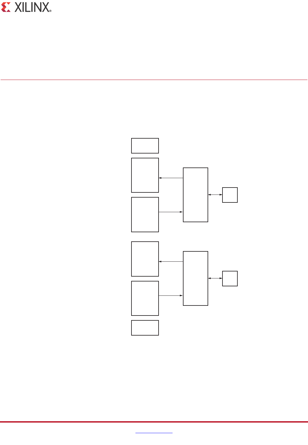
I/O Tile Overview
A Spartan®-6 FPGA I/O tile contains two IOBs, two ILOGICs, two OLOGICs, and two
IODELAYs. Figure 1-1 shows an I/O tile.
X-Ref Target - Figure 1-1
Figure 1-1: Spartan-6 FPGA I/O Tile
ug381_c1_01_041709
ILOGIC2
(Chapter 2)
or
ISERDES2
(Chapter 3)
OLOGIC2
(Chapter 2)
or
OSERDES2
(Chapter 3)
IODELAY2
(Chapter 2)
IODELAY2
(Chapter 2)
IOB
(Chapter 1) Pad
ILOGIC2
(Chapter 2)
or
ISERDES2
(Chapter 3)
OLOGIC2
(Chapter 2)
or
OSERDES2
(Chapter 3)
IOB
(Chapter 1) Pad
12 www.xilinx.com Spartan-6 FPGA SelectIO Resources
UG381 (v1.7) October 21, 2015
Chapter 1: SelectIO Resources
SelectIO Resources Introduction
All Spartan-6 FPGAs have configurable high-performance SelectIO™ drivers and
receivers, supporting a wide variety of standard interfaces. The robust feature set includes
programmable control of output strength and slew rate, and on-chip termination.
Each IOB contains both input, output, and 3-state SelectIO drivers. These drivers can be
configured to various I/O standards. Differential I/O uses the two IOBs grouped together
in one tile.
• Single-ended I/O standards (LVCMOS, LVTTL, HSTL, SSTL, PCI)
• Differential I/O standards (LVDS, RSDS, TMDS, Differential HSTL and SSTL)
• Differential and VREF dependent inputs are powered by VCCAUX
Each Spartan-6 FPGA I/O tile contains two IOBs, and also two ILOGIC blocks and two
OLOGIC blocks, as described in Chapter 2, SelectIO Logic Resources.
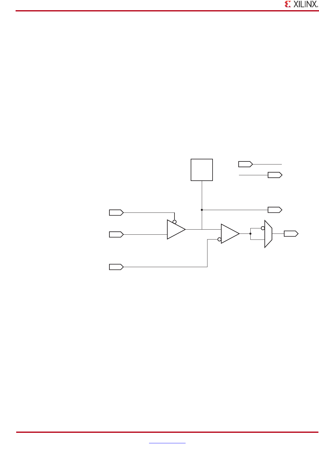
Figure 1-2 shows the basic IOB and its connections to the internal logic and the device Pad.
Each IOB has a direct connection to an ILOGIC/OLOGIC pair containing the input and
output logic resources for data and 3-state control for the IOB. Both ILOGIC and OLOGIC
can be configured as ISERDES and OSERDES, respectively, as described in Chapter 3,
Advanced SelectIO Logic Resources.
X-Ref Target - Figure 1-2
Figure 1-2: Basic IOB Diagram
ug381_c1_02_111309
PADOUT
DIFFO_IN
DIFFO_OUT
I
T
O
DIFFI_IN
OUTBUF INBUF
PA D
Spartan-6 FPGA SelectIO Resources www.xilinx.com 13
UG381 (v1.7) October 21, 2015
SelectIO Resources General Guidelines
SelectIO Resources General Guidelines
This section summarizes the general guidelines to be considered when designing with the
SelectIO™ resources in Spartan-6 FPGAs.
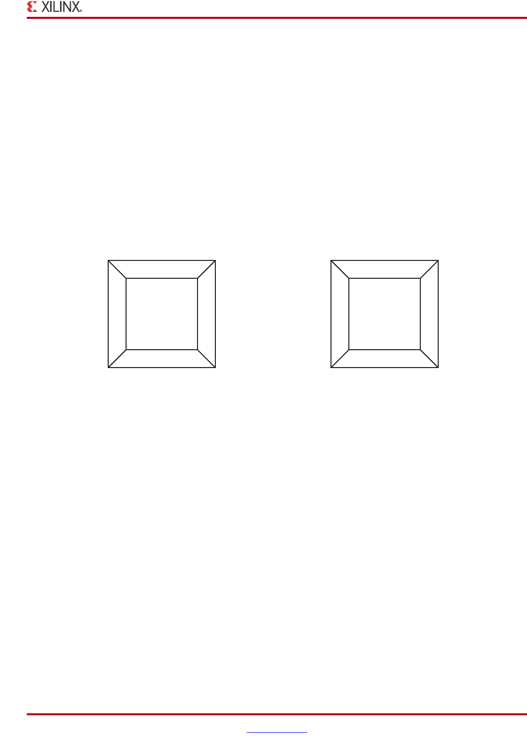
Spartan-6 FPGA SelectIO Banks
Each Spartan-6 device contains either four or six I/O banks depending on device size and
package (Figure 1-3). See the Spartan-6 Family Overview for device selection details.
• XC6SLX45/XC6SLX45T and smaller and all devices in the 484 pin packages have four
banks, one on each side of the device.
• XC6SLX75/XC6SLX75T and larger (except in the 484 pin packages) have two banks
on the left and right sides for a total of six I/O banks.
Output Drive Source Voltage (VCCO) Pins
Many of the low-voltage I/O standards supported by Spartan-6 devices require a different
output drive voltage (VCCO). As a result, each device often supports multiple output drive
source voltages.
Output buffers within a given VCCO bank must share the same output drive source
voltage. The following I/O standards input buffers also use the VCCO voltage supply:
• LVCMOS25 (when VCCAUX =3.3V)
• LVCMOS18_JEDEC
• LVCMOS15_JEDEC
• LVCMOS12_JEDEC
•PCI
• MOBILE_DDR
X-Ref Target - Figure 1-3
Figure 1-3: Spartan-6 FPGA I/O Banks
ug381_c1_03_111209
BANK0
BANK2
BANK3BANK1
LX4, LX9, LX16, LX25, LX25T, LX45, LX45T
and all devices in the 484-pin packages
BANK0
BANK2
BANK3BANK1
BANK4 BANK5
LX75, LX75T, LX100, LX100T, LX150, LX150T
except devices in the 484-pin packages
14 www.xilinx.com Spartan-6 FPGA SelectIO Resources
UG381 (v1.7) October 21, 2015
Chapter 1: SelectIO Resources
Internal Termination
Termination resistors are often required when using high-speed I/O standards for
switching level optimization and signal integrity. Termination resistors need to be kept as
close to the receivers as possible to minimize signal integrity issues. Specific design
guidelines are necessary when interfacing to wide buses with tight layouts. Although PCB
layouts can be adjusted by discrete resistors, there will always be a stub between the
discrete resistor and the device’s input buffer.
Spartan-6 FPGAs provide termination resistors for both differential interfaces (e.g, LVDS)
and single-ended interfaces (e.g., SSTL). By placing the termination resistors within the
IOB, external termination resistors can be eliminated.
Differential Termination
Differential Termination Benefits
• 100Ω parallel termination resistor for differential inputs
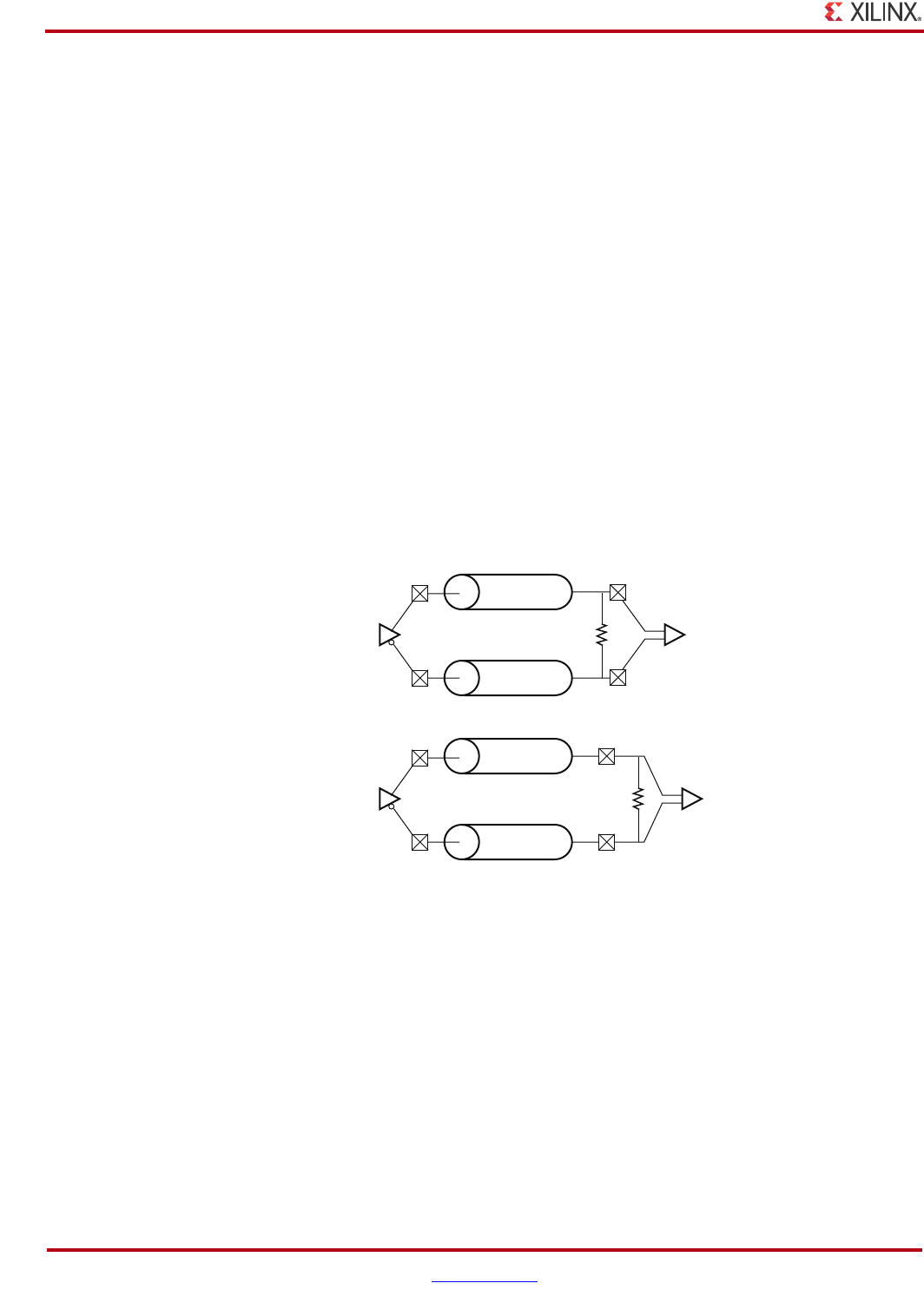
The optional Spartan-6 FPGA on-chip input differential termination eliminates any need to
use the external 100Ω termination resistors found in differential receiver circuits
(Figure 1-4). No tuning is needed. Differential termination is ideally suited for LVDS, mini-
LVDS, PPDS, and RSDS.
On-chip differential termination is specified with a nominal value of 100Ω when
VCCAUX = 3.3V. The on-chip differential termination can be used when VCCAUX =2.5V,
however a wider resistance range is specified. See the Spartan-6 FPGA Data Sheet for
specific values. Figure 1-5 shows examples of using either the optional differential
termination or an external termination resistor for a differential receiver implemented in
the Spartan-6 FPGAs.
X-Ref Target - Figure 1-4
Figure 1-4: Differential Inputs and Outputs
100Ω
100Ω
Differential
Output
Differential Input
with On-Chip
Differential Termination
Differential
Input
Differential
Output
ug381_c1_04_041709
Z0 = 50Ω
Z0 = 50Ω
Z0 = 50Ω
Z0 = 50Ω
Spartan-6 FPGA SelectIO Resources www.xilinx.com 15
UG381 (v1.7) October 21, 2015
Internal Termination
The DIFF_TERM attribute is set to TRUE to enable differential termination on a differential
I/O pin pair. This attribute uses the following syntax when used as a constraint in the UCF:
NET <I/O_NAME> DIFF_TERM = "<TRUE/FALSE>";
See Table 1-6, page 41 for bank compatibility of differential drivers, receivers, and optional
on-chip differential termination.
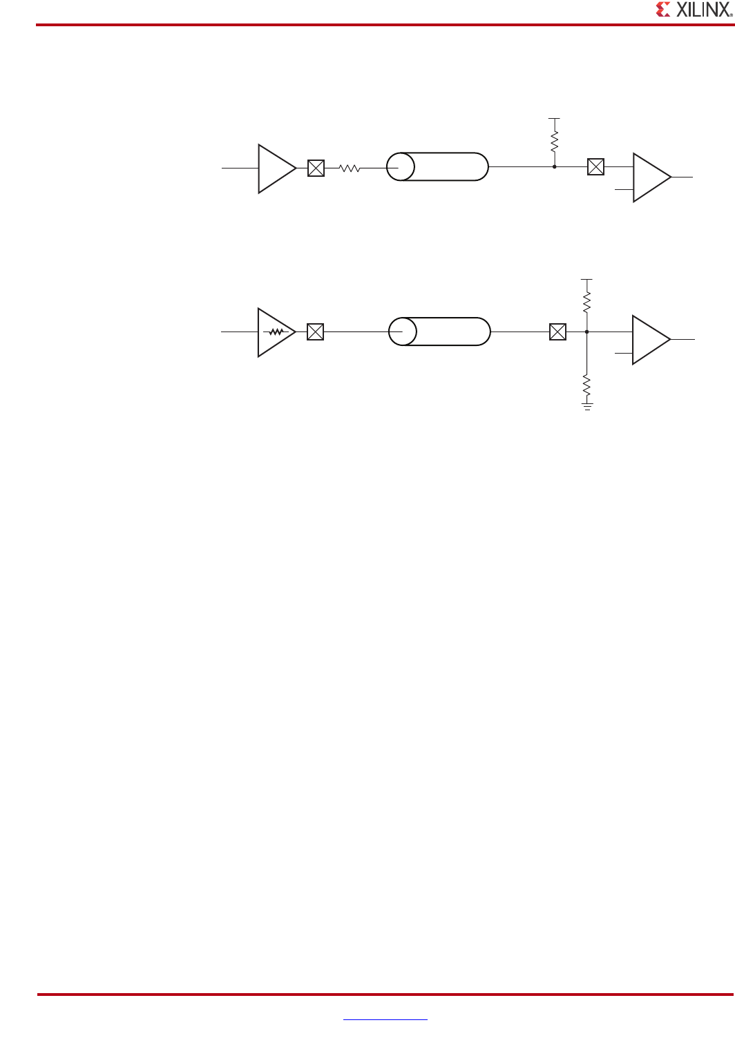
On-Chip Termination
Programmable input termination resistors and output driver impedance for single-ended
standards.
On-Chip Termination Benefits
Optional on-chip termination features in Spartan-6 FPGAs eliminate complex external
board termination schemes for high-speed single-ended signaling, such as those
commonly found in memory interfaces. Figure 1-6 shows an example of how on-chip
termination can remove the external termination resistors that can be found on a
unidirectional SSTL18 interface, such as a DDR2 SDRAM interface for address and control
pins. On-chip termination can optionally be used in the form of either programmable input
termination resistors and/or programmable output driver impedance (source
termination). Signal integrity simulations are always recommended for analyzing and
optimizing the I/O interfaces, and determining the best combination of programmable
I/O standards, optional internal termination features, and external termination
components. The best methodologies include using the Xilinx IBIS models, combined with
models for the other components on the board, and running IBIS signal integrity
simulations.
X-Ref Target - Figure 1-5
Figure 1-5: Input Termination Resistor Options for LVDS, RSDS, MINI_LVDS, and
PPDS I/O Standards
Z0 = 50Ω
Z0 = 50Ω
Z0 = 50Ω
Z0 = 50Ω
100Ω
ug381_1_05_041709
a) Differential pairs with receivers using DIFF_TERM = FALSE constraint
b) Differential pairs with receivers using DIFF_TERM = TRUE constraint
DIFF_TERM = FALSE
DIFF_TERM = TRUE
RDT
Bank 0
Bank 2
Bank 0
Bank 2
Bank 4
Bank 3
Bank 5
Bank 1
Bank 0 and 2 Any Bank
16 www.xilinx.com Spartan-6 FPGA SelectIO Resources
UG381 (v1.7) October 21, 2015
Chapter 1: SelectIO Resources
Programmable Output Driver Impedance (Source Termination)
Programmable output driver impedance helps to eliminate reflections while avoiding the
need to use external source termination resistors in high-speed single-ended signaling
applications. The driver impedance is set through the use of the OUT_TERM attribute,
using NONE (default), UNTUNED_25, UNTUNED_50, or UNTUNED_75 to force the
output driver’s impedance to be equal to the transmission line impedance of the printed
circuit board signal trace. Setting the OUT_TERM attribute to one of these values will
override the default value of NONE, and will also override all drive-strength and slew-
rates that the output buffer would have been set to for the assigned I/O standard. For
example, a bidirectional I/O assigned as LVCMOS25, 12 mA drive, slow slew rate, and
OUT_TERM = UNTUNED_50 would still have the input buffer set at LVCMOS25, but the
output buffer would no longer be configured for 12 mA drive and slow slew rate. Only
NONE (default), UNTUNED_50, or UNTUNED_75 are allowed for OUT_TERM when
VCCO is 1.2V or 1.5V in Bank 0 or Bank 2. In this case, UNTUNED_25 is not allowed.
The Spartan-6 FPGA programmable output driver impedance feature is similar to the DCI
feature available in many other Xilinx FPGA families. However, an important difference is
that the programmable output driver impedance is not calibrated, and therefore some
variation to the target output impedance value will exist across process, temperature, and
voltage variations. Proper evaluation of the system should always include signal integrity
analysis, ideally by using Xilinx IBIS models and running IBIS simulations.
X-Ref Target - Figure 1-6
Figure 1-6: Unidirectional SSTL18 Interface Using On-Chip Termination
SSTL18
SSTL18
ug381_1_06_110509
VTT
50Ω
50Ω
100Ω
100Ω
VCCO
SSTL18
SSTL18
+
–
+
–
Typical External Resistors Used For a Unidirectional SSTL18 Interface
The Same Interface Using Optional Spartan-6 FPGA
On-Chip Termination Features At Both Ends
20Ω
Z0 = 50Ω
Z0 = 50Ω
OUT_TERM = UNTUNED_50 IN_TERM = UNTUNED_SPLIT_50
Spartan-6 FPGA SelectIO Resources www.xilinx.com 17
UG381 (v1.7) October 21, 2015
Internal Termination
Figure 1-7 illustrates a controlled impedance driver in a Spartan-6 device.
To implement programmable output driver impedance on a given output pin, apply the
OUT_TERM attribute and set it to equal the desired target value. This attribute uses the
following syntax when specified as a constraint in the UCF:
NET <NET NAME> OUT_TERM = <NONE/ UNTUNED_25 / UNTUNED_50 / UNTUNED_75>;
Programmable Input Termination Resistors (Split Termination)
Some I/O standards (e.g., HSTL and SSTL) require input termination to help improve
signal integrity for high-speed single-ended signaling (see Figure 1-8). Spartan-6 FPGA
I/Os contain optional on-chip input termination resistors that can reduce the need for
external resistors. The programmable input termination resistors are available for all of the
single-ended I/O standards. The structure is that of a pull-up and pull-down resistor in
parallel, providing a Thevenin-equivalent termination resistance to a VCCO/2 level. The
IN_TERM attribute can be set to NONE (default), UNTUNED_SPLIT_25,
UNTUNED_SPLIT_50, or UNTUNED_SPLIT_75. The input termination resistors will
always be present whenever the I/O is 3-stated, and instantly turned off when the output
buffer is enabled.
The Spartan-6 FPGA programmable input termination feature is similar to the DCI feature
available in many other Xilinx FPGA families. However, an important difference is that the
programmable input termination is not calibrated, and therefore some variation to the
target resistance values will exist. See the DC specification tables in the Spartan-6 FPGA
Data Sheet for more details. Proper evaluation of the system should always include signal
integrity analysis, ideally by using Xilinx IBIS models and running IBIS simulations.
X-Ref Target - Figure 1-7
Figure 1-7: Programmable Output Driver Impedance
ug381_c1_07_060509
R
OUT_TERM = UNTUNED_<25,50,75>
where 25, 50, or 75 is the value for R in Ω.
X-Ref Target - Figure 1-8
Figure 1-8: Input Termination for Split Termination
2R
2R
UG381_c1_08_060509
V
CCO
R
V
CCO
/2
IN_TERM = UNTUNED_SPLIT_<25,50,75>
where 25, 50, or 75 is the value for R in Ω.

18 www.xilinx.com Spartan-6 FPGA SelectIO Resources
UG381 (v1.7) October 21, 2015
Chapter 1: SelectIO Resources
To implement programmable input termination resistors on a given input pin, apply the
IN_TERM attribute and set it to equal the desired target value. This attribute uses the
following syntax when specified as a constraint in the UCF:
NET <NET NAME> IN_TERM = <NONE / UNTUNED_SPLIT_25 / UNTUNED_SPLIT_50 /
UNTUNED_SPLIT_75>;
Note: IN_TERM = UNTUNED_SPLIT_25 is not supported in Bank 0 and Bank 2 when these banks
use 1.2V or 1.5V I/O standards (VCCO = 1.2V or 1.5V).
Spartan-6 FPGA SelectIO Primitives
The Xilinx software library includes an extensive list of primitives to support a variety of
I/O standards available in the Spartan-6 FPGA I/O primitives. The following are five
generic primitive names representing most of the available single-ended I/O standards.
•IBUF (input buffer)
• IBUFG (clock input buffer)
•OBUF (output buffer)
• OBUFT (3-state output buffer)
•IOBUF (input/output buffer)
These seven generic primitive names represent most of the available differential I/O
standards:
•IBUFDS (input buffer)
• IBUFGDS (clock input buffer)
•IBUFDS_DIFF_OUT (input buffer with inverted output)
• IBUFGDS_DIFF_OUT (clock input buffer with inverted output)
•OBUFDS (output buffer)
• OBUFTDS (3-state output buffer)
• IOBUFDS (input/output buffer)
IBUF and IBUFG
Signals used as inputs to Spartan-6 devices must use an input buffer (IBUF). The generic
Spartan-6 FPGA IBUF primitive is shown in Figure 1-9.
The IBUF and IBUFG primitives are the same. IBUFGs are used when an input buffer is
used as a clock input. In the Xilinx software tools, an IBUFG is automatically placed at
clock input sites.
Consult the Spartan-6 FPGA Clock Resources User Guide for additional information clock
requirements for achieving optimal performances.
X-Ref Target - Figure 1-9
Figure 1-9: Input Buffer (IBUF/IBUFG) Primitives
ug381_c1_09_051209
IBUF/IBUFG
O (Output)
into FPGA
I (Input)
From device pad
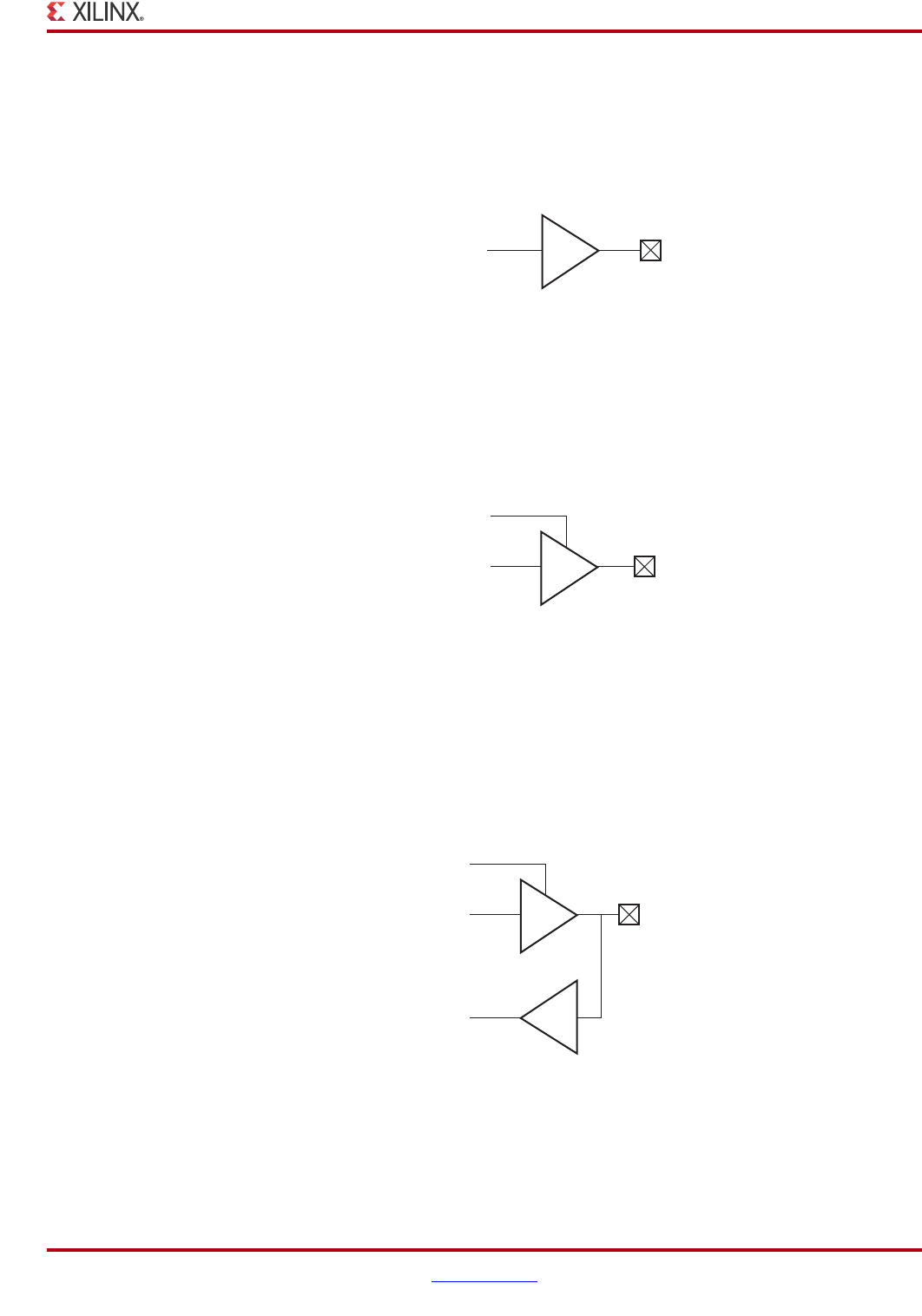
Spartan-6 FPGA SelectIO Resources www.xilinx.com 19
UG381 (v1.7) October 21, 2015
Spartan-6 FPGA SelectIO Primitives
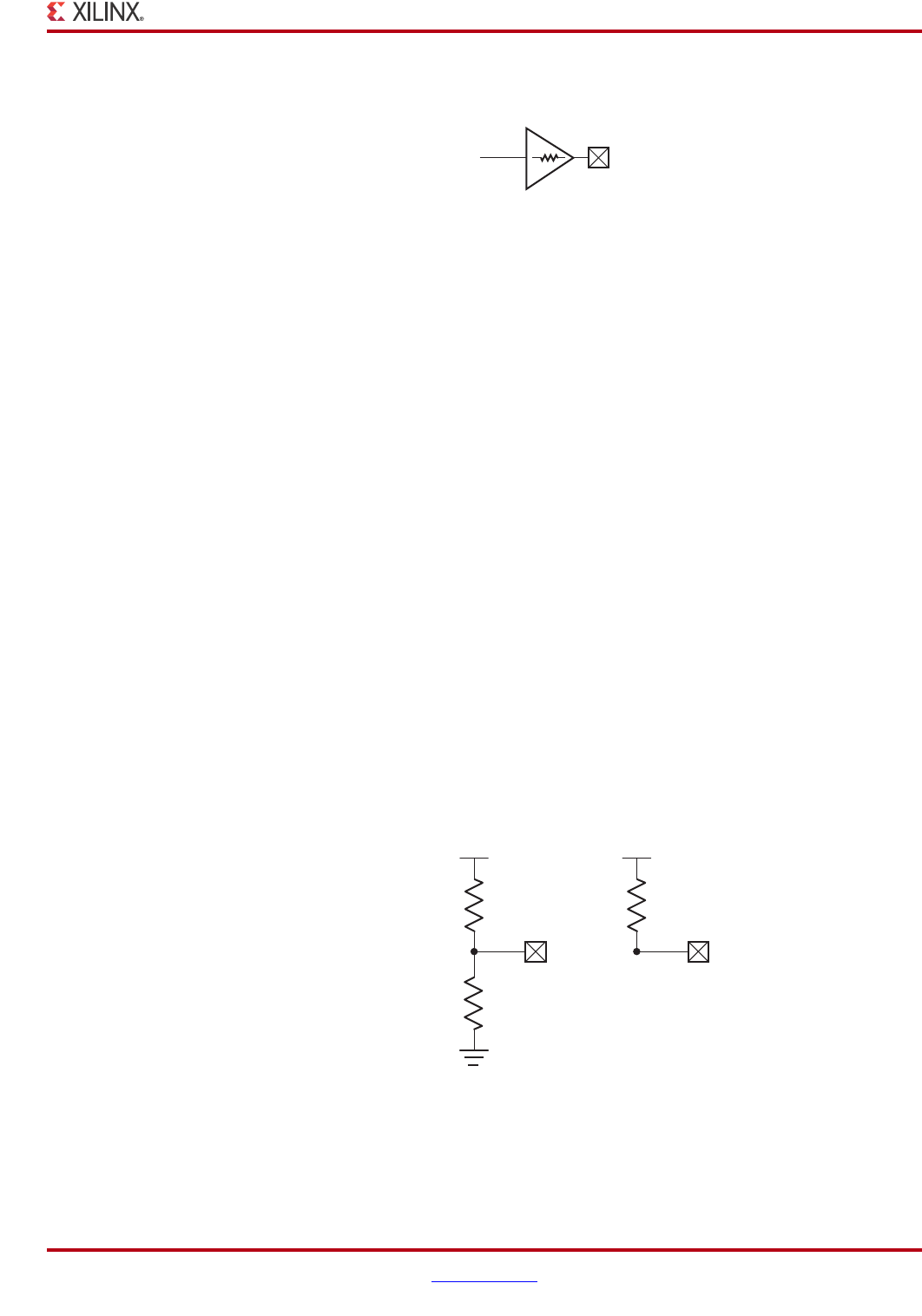
OBUF
An output buffer (OBUF) must be used to drive signals from Spartan-6 devices to external
output pads. A generic Spartan-6 FPGA OBUF primitive is shown in Figure 1-10.
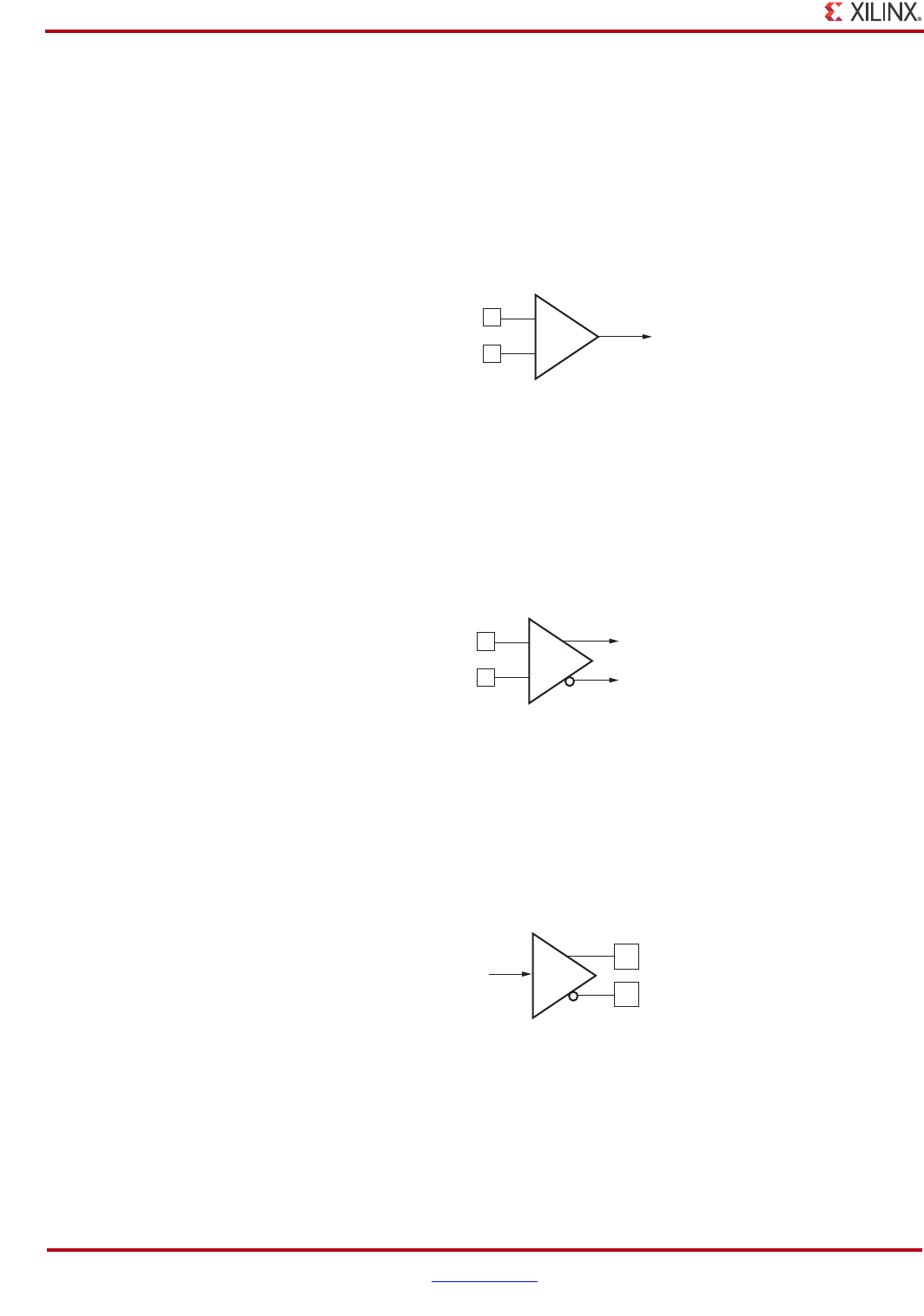
OBUFT
The generic 3-state output buffer OBUFT, shown in Figure 1-11, typically implements
3-state outputs or bidirectional I/O.
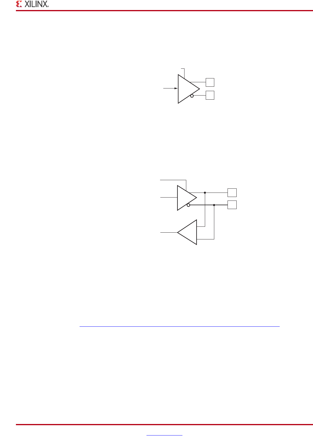
IOBUF
The IOBUF primitive is needed when bidirectional signals require both an input buffer and
a 3-state output buffer with an active High 3-state pin. Figure 1-12 shows a generic
Spartan-6 FPGA IOBUF.
X-Ref Target - Figure 1-10
Figure 1-10: Output Buffer (OBUF) Primitive
ug381_c1_10_051209
OBUF
O (Output)
to device pad
I (Input)
From FPGA
X-Ref Target - Figure 1-11
Figure 1-11: 3-State Output Buffer (OBUFT) Primitive
ug381_c1_11_051209
OBUFT
O (Output)
to device pad
I (Input)
From FPGA
T
3-state input
X-Ref Target - Figure 1-12
Figure 1-12: Input/Output Buffer (IOBUF) Primitive
ug381_c1_12_051209
IOBUF
I/O
to/from device pad
I (Input)
from FPGA
O (Output)
to FPGA
T
3-state input
20 www.xilinx.com Spartan-6 FPGA SelectIO Resources
UG381 (v1.7) October 21, 2015
Chapter 1: SelectIO Resources
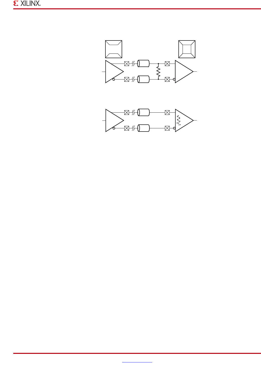
IBUFDS and IBUFGDS
The usage and rules corresponding to the differential primitives (with DS in the name) are
similar to the single-ended SelectIO primitives. Differential SelectIO primitives have two
pins to and from the device pads to show the P and N channel pins in a differential pair. N
channel pins have a B suffix.
Figure 1-13 shows the differential input buffer primitive.
IBUFDS_DIFF_OUT and IBUFGDS_DIFF_OUT
Figure 1-14 shows the differential input buffer with differential outputs to the FPGA logic.
OBUFDS
Figure 1-15 shows the differential output buffer primitive.
X-Ref Target - Figure 1-13
Figure 1-13: Differential Input Buffer Primitive
(IBUFDS and IBUFGDS)
ug381_c1_13_111909
+
–
I
IB
O
IBUFDS and IBUFGDS
Inputs from
device pads
Output to
FPGA
X-Ref Target - Figure 1-14
Figure 1-14: Differential Input Buffer Primitive with Differential Outputs
(IBUFDS_DIFF_OUT and IBUFGDS_DIFF_OUT)
ug381_c1_14new_051810
+
–
I
IB
IBUFDS_DIFF_OUT and IBUFGDS_DIFF_OUT
Inputs from
device pads
Outputs to
FPGA
OB
O
X-Ref Target - Figure 1-15
Figure 1-15: Differential Output Buffer Primitive (OBUFDS)
ug381_c1_14_051209
+
–OB
O
I
OBUFDS
Input from
FPGA
Output to
Device Pads
Spartan-6 FPGA SelectIO Resources www.xilinx.com 21
UG381 (v1.7) October 21, 2015
Spartan-6 FPGA SelectIO Primitives
OBUFTDS
Figure 1-16 shows the differential 3-state output buffer primitive.
IOBUFDS
Figure 1-17 shows the differential input/output buffer primitive.
Spartan-6 FPGA SelectIO Attributes/Constraints
Access to some Spartan-6 FPGA I/O resource features (e.g., location constraints, input
delay, output drive strength, and slew rate) is available through the attributes/constraints
associated with these features. For more information, the Constraints Guide is available on
the Xilinx web site with syntax examples and VHDL/Verilog reference code. This guide is
available inside the Software Manuals at:
www.xilinx.com/support/documentation/sw_manuals/xilinx14_7/cgd.pdf
All of the I/O resource features can be implemented in the design using at least two
different methods:
• Specifying them in the VHDL/Verilog design in the form of attributes added to the
instantiation lines of the input or output buffer primitives, or to the I/O port net.
• Specifying them in the UCF file in the form of constraints specified on the I/O port
net.
For simplicity, the examples provided in this section are for adding the features as
constraints added to the design UCF file. For more details on the method of adding
attributes in VHDL or Verilog designs, refer to the Constraints Guide.
X-Ref Target - Figure 1-16
Figure 1-16: Differential 3-state Output Buffer Primitive (OBUFTDS)
ug381_c1_15_051209
+
–OB
O
I
T
OBUFTDS
Input from
FPGA
3-state Input
Output to
Device Pads
X-Ref Target - Figure 1-17
Figure 1-17: Differential Input/Output Buffer Primitive (IOBUFDS)
ug381_c1_16_111309
IOBUFDS
I/O
to/from
device pad
I (Input)
from FPGA
O (Output)
to FPGA
T
3-state Input
+
–
+
–
IO
IOB

22 www.xilinx.com Spartan-6 FPGA SelectIO Resources
UG381 (v1.7) October 21, 2015
Chapter 1: SelectIO Resources
The PULLUP/PULLDOWN/KEEPER features have another method of implementation,
which is actually the preferred method, where the PULLUP, PULLDOWN, or KEEPER
primitives are instantiated directly into the source VHDL/Verilog design. This method is
the only way that the effect of these features (PULLUP, PULLDOWN, or KEEPER) can be
included in the HDL simulations of the design. For more information, see the Spartan-6
FPGA Libraries Guide for HDL Designs.
Location Constraint
The location constraint (LOC) must be used to specify the I/O location of an instantiated
I/O primitive. The possible values for the location constraint are all the external port
identifiers (e.g., A8, M5, AM6, etc.). These values are device and package size dependent.
The LOC attribute uses the following syntax when specified as a constraint in the UCF file:
NET <I/O_NAME> LOC = "<EXTERNAL_PORT_IDENTIFIER>";
Example:
NET MY_IO LOC=R7;
IOSTANDARD Attribute
The IOSTANDARD attribute is available to choose the values for an I/O standard for all
I/O buffers. The IOSTANDARD attribute uses the following syntax when specified as a
constraint in the UCF file:
NET <I/O_NAME> IOSTANDARD=”<IOSTANDARD VALUE>”;
The IOSTANDARD default for single-ended I/O is LVCMOS25, for differential I/Os the
default is LVDS_25.
Output Slew Rate Attribute
A variety of attribute values provide the option of choosing the desired slew rate for
single-ended I/O output buffers. For LVTTL and LVCMOS output buffers (OBUF, OBUFT,
and IOBUF), the desired slew rate can be specified with the SLEW attribute.
The allowed values for the SLEW attribute are:
• SLEW = SLOW (Default)
• SLEW = FAST
• SLEW = QUIETIO
The SLEW attribute uses the following syntax when specified as a constraint in the UCF
file:
NET <I/O_NAME> SLEW = "<SLEW_VALUE>";
The default slew rate for each output buffer is SLOW. This is the default used to minimize
the power bus transients when switching non-critical signals.

Spartan-6 FPGA SelectIO Resources www.xilinx.com 23
UG381 (v1.7) October 21, 2015
Spartan-6 FPGA SelectIO Primitives
Output Drive Strength Attribute
For LVTTL and LVCMOS output buffers (OBUF, OBUFT, and IOBUF), the desired drive
strength (in mA) can be specified with the DRIVE attribute.
The allowed values for the DRIVE attribute are:
•DRIVE = 2
•DRIVE = 4
•DRIVE = 6
•DRIVE = 8
• DRIVE = 12 (Default)
•DRIVE = 16
•DRIVE = 24
LVCMOS12 only supports the 2, 4, 6, 8, and 12 mA DRIVE settings. LVCMOS15 only
supports the 2, 4, 6, 8, 12, and 16 mA DRIVE settings.
The DRIVE attribute uses the following syntax when specified as a constraint in the UCF
file:
NET <I/O_NAME> DRIVE = "<DRIVE_VALUE>";
Refer to Table 1-2 for bank-specific restrictions.
PULLUP/PULLDOWN/KEEPER for IBUF, OBUFT, and IOBUF
When using 3-state output (OBUFT) or bidirectional (IOBUF) buffers, the output can have
a weak pull-up resistor, a weak pull-down resistor, or a weak “keeper” circuit. For input
(IBUF) buffers, the input can have either a weak pull-up resistor or a weak pull-down
resistor. This feature can be invoked by adding the following possible constraint values to
the relevant net of the buffers:
• PULLUP
• PULLDOWN
•KEEPER
The attribute uses the following syntax when specified as a constraint in the UCF file:
NET <I/O_NAME> <PULLUP/PULLDOWN/KEEPER>;
Differential Termination Attribute
The differential termination (DIFF_TERM) attribute is designed for the Spartan-6 FPGA
supported differential input I/O standards. It is used to turn the built-in, 100Ω, differential
termination on or off.
The allowed values for the DIFF_TERM attribute are:
•TRUE
•FALSE (Default)
The DIFF_TERM attribute uses the following syntax when specified as a constraint in the
UCF file:
NET <IO_NAME> DIFF_TERM = "<TRUE/FALSE>";
24 www.xilinx.com Spartan-6 FPGA SelectIO Resources
UG381 (v1.7) October 21, 2015
Chapter 1: SelectIO Resources
Input and Output Termination
The On-Chip Termination section discusses the IN_TERM and OUT_TERM syntax for
inclusion in the UCF.
SelectIO Signal Standards
The Input/Output Blocks (IOBs) feature inputs and outputs that support a wide range of
single-ended I/O signaling standards. The majority of the I/Os also can be used to form
differential pairs to support any of the differential signaling standards. This flexibility
allows the user to select the best I/O standard on each pin that meets the interface and
signal integrity requirements of the application.
The I/O pins are separated into independent banks, typically four or six per device. Each
bank has a common output voltage supply (VCCO) and a common reference voltage for
HSTL and SSTL standards (VREF). The banks are numbered as shown in Figure 1-1.
Overview of I/O Standards
Modern bus applications, pioneered by the largest and most influential companies in the
digital electronics industry, are commonly introduced with a new I/O standard tailored
specifically to the needs of that application. The bus I/O standards provide specifications
to other vendors who create products designed to interface with these applications. Each
standard often has its own specifications for current, voltage, I/O buffering, and
termination techniques.
The ability to provide the flexibility and time-to-market advantages of programmable logic
dependents on the capability of programmable logic devices to support an increasing
variety of I/O standards. The SelectIO resources feature highly configurable input and
output buffers supporting for a wide variety of I/O standards.
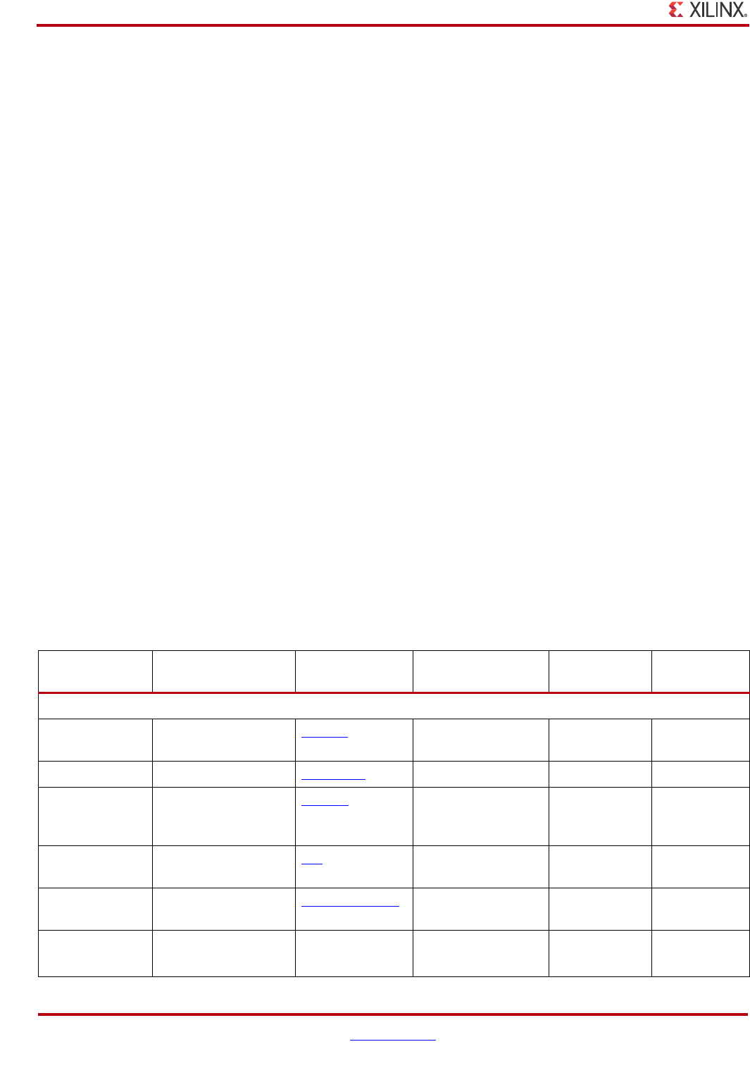
Table 1-1 provides a brief overview of the I/O standards supported by Spartan-6 FPGAs,
including the sponsors and common uses for the standard. The standard numbers are
indicated where appropriate.
Table 1-1: I/O Signaling Standards
Standard Description Industry
Specification Use and Sponsor Input Buffer Output Buffer
Single-Ended Standards
LVTTL Low Voltage TTL JESD8C General purpose
3.3V
LVTTL Push-Pull
LVCMOS Low Voltage CMOS JESD8C-01 General purpose CMOS Push-Pull
PCI Peripheral
Component
Interconnect
PCI SIG PCI bus LVTTL Push-Pull
I2C Inter Integrated
Circuit
I2C NXP CMOS Open drain
SMBUS System Management
Bus
www.smbus.org Intel CMOS Open drain
SDIO Secure Digital Input
Output
SDIO
JESD8-1A
SD Card Assoc,
Memory Card
CMOS Push-Pull
Spartan-6 FPGA SelectIO Resources www.xilinx.com 25
UG381 (v1.7) October 21, 2015
SelectIO Signal Standards
Mobile DDR Low Power DDR JESD209A CMOS Push-Pull
HSTL High-Speed
Transceiver Logic
JESD8-6 Hitachi SRAM; IBM;
three of four classes
supported
VREF based Push-Pull
HSTL18 High-Speed
Transceiver Logic
JESD8-6 Hitachi SRAM; IBM;
three of four classes
supported
VREF based
SSTL3 Stub Series
Terminated Logic for
3.3V
JESD8-8 SDRAM bus; Hitachi
and IBM; two classes
VREF based Push-Pull
SSTL2 SSTL for 2.5V JESD8-9 DDR SDRAM VREF based Push-Pull
SSTL18 SSTL for 1.8V JESD79-2C DDR2 SDRAM VREF based Push-Pull
SSTL15 SSTL for 1.5V JESD79-3 DDR3 SDRAM VREF based Push-Pull
Differential Standards
LVDS25
LVDS33
Low Voltage
Differential Signaling
ANSI/TIA/EIA-
644-A
High-speed
interface, backplane,
video; National, TI
Differential
Pair
Differential
Pair
BLVDS Bus LVDS ANSI/TIA/EIA-
644-A
Bidirectional,
multipoint LVDS
Differential
Pair
Pseudo
Differential
Pair
DISPLAY PORT Auxiliary channel
interface for DISPLAY
PORT
www.vesa.org Flat panel displays Differential
Pair
Pseudo
Differential
Pair
LVPECL Low Voltage Positive
ECL
Freescale
Semiconductor
(formerly
Motorola)
High-speed clocks Differential
Pair
N/A
MINI_LVDS mini-LVDS TI, Display panel
interface
Flat panel displays Differential
Pair
Differential
Pair
RSDS Reduced Swing
Differential Signaling
National
Semiconductor
Flat panel displays Differential
Pair
Differential
Pair
TMDS Transition Minimized
Differential Signaling
National, Display
panel interface
Silicon Image;
DVI/HDMI
Differential
Pair
Differential
Pair
PPDS Point-to-Point
Differential Signaling
National, Display
panel interface
LCDs Differential
Pair
Differential
Pair
Differential
Mobile DDR
Differential LPDDR
for CK/CK#
JESD209A Differential
Pair
Pseudo
Differential
Pair
Table 1-1: I/O Signaling Standards (Cont’d)
Standard Description Industry
Specification Use and Sponsor Input Buffer Output Buffer
26 www.xilinx.com Spartan-6 FPGA SelectIO Resources
UG381 (v1.7) October 21, 2015
Chapter 1: SelectIO Resources
LVTTL—Low-Voltage TTL
The Low-Voltage TTL (LVTTL) standard is a general-purpose EIA/JESD standard for 3.3V
applications that uses an LVTTL input buffer and a push-pull output buffer. This standard
requires a 3.3V output source voltage (VCCO), but does not require the use of a reference
voltage (VREF) or a termination voltage (VTT).
LVCMOS—Low-Voltage CMOS
The Low-Voltage CMOS standard is used for general-purpose applications at voltages
from 1.2V to 3.3V. This standard does not require the use of a reference voltage (VREF) or a
board termination voltage (VTT).
LVCMOS_JEDEC—Low-Voltage CMOS with JEDEC Compliant Inputs
LVCMOS_JEDEC are alternate versions of the 1.2V, 1.5V, and 1.8V LVCMOS interfaces. The
input buffers are powered from the VCCO rail to align the VINL and VINH with the JEDEC®
input requirements. The Spartan-6 FPGA Data Sheet contains the VINL and VINH
specifications. The LVCMOS_JEDEC standards are can be the preferred interface to ASSPs
or ASICs. However, when interfacing with other Xilinx FPGAs, use the non-JEDEC
LVCMOS standards.
PCI—Peripheral Component Interface
The Peripheral Component Interface (PCI) standard specifies support for 33 MHz PCI bus
applications. It uses an LVTTL input buffer and a push-pull output buffer. This standard
does not require the use of a reference voltage (VREF) or a board termination voltage (VTT);
however, it does require a 3.3V output source voltage (VCCO).
I2C—Inter-Integrated Circuit Bus
The I2C bus is a multi-master interface allowing multiple devices to be connected to a
simple four-wire interface. Developed by Philips, the I2C bus supports low speed
(100 kb/s), Fast (400 kb/s), and high-speed (3.4 Mb/s) data rates. This standard is an open
drain output requiring external pull-up resistors. When using I2C as an output in the
Spartan-6 device, the open drain is automatically created with all pull-up legs turned off.
DIFF_HSTL_I
DIFF_HSTL_III
DIFF_HSTL_IV
DIFF_HSTL_I_18
DIFF_HSTL_III_18
DIFF_HSTL_IV_18
Pseudo Differential
HSTL
JESD8-6 SRAM Differential
Pair
Pseudo
Differential
Pair
DIFF_SSTL3_I
DIFF_SSTL3_II
DIFF_SSTL2_I
DIFF_SSTL2_II
DIFF_SSTL18_I
DIFF_SSTL18_II
DIFF_SSTL15_II
Pseudo Differential
SSTL
JESD8-9
JESD79-2C
JESD79-3
DDR, DDR2,
DDR3 SDRAM
Differential
Pair
Pseudo
Differential
Pair
Table 1-1: I/O Signaling Standards (Cont’d)
Standard Description Industry
Specification Use and Sponsor Input Buffer Output Buffer

Spartan-6 FPGA SelectIO Resources www.xilinx.com 27
UG381 (v1.7) October 21, 2015
SelectIO Signal Standards
SMBUS—System Management Bus
System Management Bus was defined by Intel and the SBS-IF to provide a simple,
commonly accepted interface to power supplies. Based on I2C, SMBUS supports data rates
up to 100 kb/s. This standard is an open drain output requiring external pull-up resistors
terminated to VTT =3.3V.
SDIO—SD Memory Card Interface
SDIO is used for interfacing to SD memory cards in 3.3V applications. This standard does
not require the use of a reference voltage (VREF) or a board termination voltage (VTT).
MOBILE_DDR—Low Power DDR
Low power memory bus interface defined by JEDEC Standard JESD209A for use with 1.8V
LPDDR or Mobile DDR memories. Using MOBILE_DDR eliminates the need for
VREF and VTT.
HSTL—High-Speed Transceiver Logic
The High-Speed Transceiver Logic (HSTL) standard is a general-purpose, high-speed 1.5V
or 1.8V bus standard sponsored by IBM. This standard has four variations or classes: Class
I, II, III, and IV. This standard requires a differential amplifier input buffer and a push-pull
output buffer.
DIFF_HSTL is supported through a combination of differential inputs and pseudo-
differential outputs.
SSTL3—Stub Series Terminated Logic for 3.3V
The Stub Series Terminated Logic standard is a general-purpose memory bus standard
sponsored by Hitachi and IBM (JESD8-8). This standard has multiple voltages from 1.8V to
3.3V, and two classes, I and II. This standard requires a differential amplifier input buffer
and a push-pull output buffer.
DIFF_SSTL3 is supported through a combination of differential inputs and pseudo-
differential outputs.
SSTL2—Stub Series Terminated Logic for 2.5V
The Stub Series Terminated Logic standard is a general-purpose memory bus standard
sponsored by Hitachi and IBM (JESD8-8). This standard has multiple voltages from 1.8V to
3.3V, and two classes, I and II. This standard requires a differential amplifier input buffer
and a push-pull output buffer.
DIFF_SSTL2 is supported through a combination of differential inputs and pseudo-
differential outputs.
SSTL18—Stub Series Terminated Logic for 1.8V
The SSTL18 standard, specified by JEDEC Standard JESD79-2C, is a general-purpose 1.8V
memory bus standard. This voltage-referenced standard requires a reference voltage of
0.90 V, an input/output source voltage of 1.8 V, and a termination voltage of 0.90 V. This
standard requires a differential amplifier input buffer and a push-pull output buffer.
SSTL18 is used for high-speed SDRAM interfaces.

28 www.xilinx.com Spartan-6 FPGA SelectIO Resources
UG381 (v1.7) October 21, 2015
Chapter 1: SelectIO Resources
DIFF_SSTL18 is supported through a combination of differential inputs and pseudo-
differential outputs.
SSTL15—Stub Series Terminated Logic for 1.5V
The SSTL15 standard, specified by JEDEC Standard JESD79-3, is a general-purpose 1.5V
memory bus standard. This voltage-referenced standard requires a reference voltage of
0.75V, an input/output source voltage of 1.5V, and a termination voltage of 0.75V. This
standard requires a differential amplifier input buffer and a push-pull output buffer.
SSTL15 is used for high-speed SDRAM interfaces.
DIFF_SSTL15 is supported through a combination of differential inputs and pseudo-
differential outputs.
LVDS_25—Low Voltage Differential Signal
LVDS_25 is used to drive TIA/EIA644 LVDS levels in a bank powered with 2.5V VCCO.
LVDS is a differential I/O standard. As with all differential signaling standards, LVDS
requires that one data bit is carried through two signal lines, and it has an inherent noise
immunity over single-ended I/O standards. The voltage swing between two signal lines is
approximately 350 mV. The use of a reference voltage (VREF) or a board termination
voltage (VTT) is not required. LVDS requires the use of two pins per input or output. LVDS
inputs require a parallel termination resistor, either through the use of a discrete resistor on
the PCB, or the use of the DIFF_TERM attribute to enable internal termination. LVDS
inputs can be placed on any I/O bank, while LVDS outputs are only available on I/O
banks 0 and 2.
LVDS_33—Low Voltage Differential Signal
LVDS_33 is used to drive TIA/EIA644 LVDS levels in a bank powered with 3.3V VCCO.
Electrically the same as LVDS_25. LVDS inputs require a parallel termination resistor,
either through the use of a discrete resistor on the PCB, or the use of the DIFF_TERM
attribute to enable internal termination. LVDS inputs can be placed on any I/O bank, while
LVDS outputs are only available on I/O banks 0 and 2.
BLVDS—Bus LVDS
Allows for bidirectional LVDS communication between two or more devices. The bus
LVDS standard requires external resistor termination as shown in Figure 1-19, page 36.
Unlike many of the other differential standards, there are no restrictions on which banks
the BLVDS standard can be used. BLVDS is supported through a combination of
differential inputs and pseudo-differential outputs.
DISPLAY_PORT—AUX CH for DisplayPort
DISPLAY_PORT is a 1 Mb/s differential signaling standard used by DisplayPort™ for
identifying, configuring and maintaining connections between DisplayPort devices. AUX
CH is a dedicated differential pair that does not cover the main link PHY. This bidirectional
standard uses a pseudo-differential outputs connected to the termination topology as
defined by DisplayPort specifications.

Spartan-6 FPGA SelectIO Resources www.xilinx.com 29
UG381 (v1.7) October 21, 2015
SelectIO Signal Standards
Mini-LVDS
A serial, intra-flat panel solution that serves as an interface between the timing control
function and an LCD source driver. Mini-LVDS inputs require a parallel termination
resistor, either through the use of a discrete resistor on the PCB, or the use of the
DIFF_TERM attribute to enable internal termination. Mini-LVDS inputs can be placed on
any I/O bank, while Mini-LVDS outputs are only available on I/O banks 0 and 2.
RSDS—Reduced Swing Differential Signaling
A signaling standard that defines the output characteristics of a transmitter and inputs of
a receiver along with the protocol for a chip-to-chip interface between flat-panel timing
controllers and column drivers. RSDS inputs require a parallel termination resistor, either
through the use of a discrete resistor on the PCB, or the use of the DIFF_TERM attribute to
enable internal termination. RSDS inputs can be placed on any I/O bank, while RSDS
outputs are only available on I/O banks 0 and 2.
TMDS—Transition Minimized Differential Signaling
Technology for transmitting high-speed serial data used by the DVI and HDMI video
interfaces. The TMDS standard requires external 50Ω resistor pull-ups to 3.3V on inputs.
TMDS inputs do not require parallel input termination resistors, and can be placed on any
I/O bank, while TMDS outputs are only available on I/O banks 0 and 2.
PPDS—Point-to-Point Differential Signaling
Differential next-generation LCD standard for interface to row and column drivers. PPDS
inputs require a parallel termination resistor, either through the use of a discrete resistor on
the PCB, or the use of the DIFF_TERM attribute to enable internal termination. PPDS
inputs can be placed on any I/O bank, while PPDS outputs are only available on I/O
banks 0 and 2.
I/O Timing Analysis
The choice of I/O standard affects the timing for the I/O pin.The adjustments are
automatically included in the timing analyzer reports generated by the Xilinx
development tools.
When measuring timing parameters at the programmable I/Os, different signal standards
call for different test conditions. The data sheet lists the conditions to use for each standard.
The method to measure input timing of a signal that swings between a logic Low level of
VL and a logic High level of VH when applied to the input under test is described in this
section. Some standards also require the application of a bias voltage to the VREF pins of a
given bank to properly set the input-switching threshold. The measurement point of the
input signal (VM) is commonly located halfway between VL and VH.
For an output test setup, one end of the termination resistor RT is connected to a
termination voltage VT and the other end is connected to the output. For each standard, RT
and VT generally take on the standard values recommended for minimizing signal
reflections. When the standard does not ordinarily use terminations (for example,
LVCMOS, LVTTL), then RT is set to 1MΩ to indicate an open connection, and VT is set to
zero. The same measurement point (VM) that was used at the input is also used at the
output.

30 www.xilinx.com Spartan-6 FPGA SelectIO Resources
UG381 (v1.7) October 21, 2015
Chapter 1: SelectIO Resources
The capacitive load (CL) is connected between the output and GND. The output timing for
all standards, as published in the speed specifications and the data sheet, is always based
on a CL value of zero. High-impedance probes (less than 1 pF) are used for all
measurements. Any delay that the test fixture could contribute to test measurements is
subtracted from the measurements used to produce the final timing numbers as published
in the speed specifications and data sheet.
Using IBIS Models to Simulate Load Conditions
IBIS models permit the most accurate prediction of timing delays for a given application.
The parameters found in the IBIS model (VREF, RREF, and VMEAS) correspond directly with
the parameters found in the data sheet (VT, RT, and VM). Do not confuse VREF (the
termination voltage) from the IBIS model with VREF (the input-switching threshold) from
the table. A fourth parameter, CREF, is always zero. The four parameters describe all
relevant output test conditions. IBIS models are found in the Xilinx development software
and at the following link: www.xilinx.com/support/download/index.htm
Delays for a given application are simulated according to specific load conditions as
follows:
1. Simulate the desired signal standard with the output driver connected to the test setup
shown in the data sheet. Use parameter values VT, RT, and VM from the data sheet;
CREF is zero.
2. Record the time to VM.
3. Simulate the same signal standard with the output driver connected to the PCB trace
with load. Use the appropriate IBIS model (including VREF, RREF, CREF, and VMEAS
values) or capacitive value to represent the load.
4. Record the time to VMEAS.
5. Compare the results of steps 2 and 4. Add (or subtract) the increase (or decrease) in
delay to (or from) the appropriate output standard adjustment to yield the worst-case
delay of the PCB trace.
LVCMOS/LVTTL Slew Rate Control and Drive Strength
Each IOB has a slew-rate control that sets the output switching edge rate for LVCMOS and
LVTTL outputs. The SLEW attribute controls the slew rate and can be set to SLOW
(default), FAST, or QUIETIO. The slowest slew rate setting (QUIETIO) provides the lowest
noise and power consumption, while the faster slew rate settings improve timing.
Each LVCMOS and LVTTL output additionally supports up to seven different drive
current strengths as shown in Table 1-2. To adjust the drive strength for each output, the
DRIVE attribute is set to the desired drive strength: 2, 4, 6, 8, 12, 16, and 24. Unless
otherwise specified in the FPGA application, the software default for IOSTANDARD is
LVCMOS25, SLOW slew rate, and 12 mA output drive.
Each method of specifying the I/O standard (schematic, HDL, constraints file,
PlanAhead™ tool) also supports specification of the LVCMOS/LVTTL DRIVE and SLEW
options.
Spartan-6 FPGA SelectIO Resources www.xilinx.com 31
UG381 (v1.7) October 21, 2015
SelectIO Signal Standards
High output current drive strength and FAST output slew rates generally result in the
fastest I/O performance. However, these same settings can also result in transmission line
effects on the PCB for all but the shortest board traces. Each IOB has independent slew rate
and drive strength controls. Use the slowest slew rate and lowest output drive current that
meets the performance requirements for the end application.
Simultaneously Switching Outputs
Due to lead inductance, a given package supports a limited number of simultaneous
switching outputs (SSOs) when using fast, high-drive outputs. Only use fast, high-drive
outputs when required by the application.
The Simultaneously Switching Outputs section in the Spartan-6 FPGA Data Sheet provides
guidelines for the recommended maximum allowable number of SSOs. These guidelines
describe the maximum number of user I/O pins of a given output signal standard that
should simultaneously switch in the same direction, while maintaining a safe level of
switching noise. Meeting these guidelines for the stated test conditions ensures that the
FPGA operates free from the adverse effects of ground and power bounce.
Ground or power bounce occurs when a large number of outputs simultaneously switch in
the same direction. The output drive transistors all conduct current to a common voltage
rail. Low-to-High transitions conduct to the VCCO rail; High-to-Low transitions conduct to
the GND rail. The resulting cumulative current transient induces a voltage difference
across the inductance that exists between the die pad and the power supply or ground
return. The inductance is associated with bonding wires, the package lead frame, and any
other signal routing inside the package. Other variables contribute to SSO noise levels,
including stray inductance on the PCB as well as capacitive loading at receivers. Any SSO-
induced voltage consequently affects internal switching noise margins and ultimately
signal quality.
For each device/package combination, the data sheet provides the number of equivalent
VCCO/GND pairs. For each output signal standard and drive strength, the data sheet
recommends the maximum number of SSOs, switching in the same direction, allowed per
VCCO/GND pair within an I/O bank. The guidelines are categorized by package style,
slew rate, and output drive current. Furthermore, the number of SSOs is specified by I/O
bank. Multiply the appropriate numbers from each table to calculate the maximum
Table 1-2: Spartan-6 FPGA Programmable Output Drive Current Supported by I/O Standard
I/O STANDARD
Output Drive Current (mA)
2 4 6 8 12 16 24
LVTTL All All All All All All All
LVCMOS33 All All All All All All All
LVCMOS25 All All All All All All Banks
1, 3, 4, 5
LVCMOS18,
LVCMOS18_JEDEC
All All All All All All Banks
1, 3, 4, 5
LVCMOS15,
LVCMOS15_JEDEC
All All All All Banks
1, 3, 4, 5
Banks
1, 3, 4, 5
N/A
LVCMOS12,
LVCMOS12_JEDEC
All All All Banks
1, 3, 4, 5
Banks
1, 3, 4, 5
N/A N/A

32 www.xilinx.com Spartan-6 FPGA SelectIO Resources
UG381 (v1.7) October 21, 2015
Chapter 1: SelectIO Resources
number of SSOs allowed within an I/O bank. Exceeding these SSO guidelines can result in
increased power or ground bounce, degraded signal integrity, or increased system jitter.
The recommended maximum SSO values assumes that the FPGA is soldered on the
printed circuit board and that the board uses sound design practices. The SSO values do
not apply for FPGAs mounted in sockets, due to the lead inductance introduced by the
socket.
The number of SSOs allowed for quad-flat packages (TQ) is lower than for ball grid array
packages (FG and CS) due to the larger lead inductance of the quad-flat packages. Ball grid
array packages are recommended for applications with a large number of simultaneously
switching outputs.
Pin-Planning to Mitigate SSO Sensitivity
When performing pin planning of a design, it is important to choose I/O pin placements
that separate strong outputs and/or simultaneously switching outputs from sensitive
inputs and outputs (particularly asynchronous inputs). Strong outputs tend to be the Class
II versions of HSTL and SSTL drivers, PCI variants, and any LVCMOS or LVTTL with
drive strengths over 8 mA. These I/O standards have smaller values in the tables that
show SSO limit per VCCO/GND pairs in the Simultaneously Switching Outputs section of the
Spartan-6 FPGA Data Sheet. Sensitive inputs and outputs can have a low noise margin and
tend to be high-speed signals, or signals where the swing is reduced by parallel receiver
termination. Since localized SSO noise in Spartan-6 FPGAs is based on the proximity of
signal wire bonds to one another, it is important to try to separate signals based on the
position of the die pads around the edge of the die, as opposed to the position of the
package solder ball. To further reduce potential noise induced from SSOs, outputs should
be distributed evenly rather than clustered in one area. As much as possible, SSOs within
a bank should be spread across the bank. Whenever possible, distribute SSOs into multiple
banks.
The PlanAhead™ tool in the ISE® software can help accomplish pin-planning to avoid
SSO sensitivity issues. By clicking on a package pin in the Package window, a
corresponding IOBS or IOBM pad is highlighted in the Device window. These IOBM and
IOBS site types represent the die pads and show the relative physical location around the
die edge. Through the use of the PlanAhead tool, intelligent pin placement can be used to
separate the die pads of pins. This is implemented by separating the die pads of pins with
strong outputs and simultaneously switching outputs from the die pads of pins with
sensitive inputs and outputs. See UG632: PlanAhead User Guide for more information on
SSO analysis and mitigation. For 7 series FPGAs, Virtex-6, and Spartan-6 devices, the
PlanAhead tool performs simultaneous switching noise (SSN) analysis. See the Running
SSN Analysis section in UG632: PlanAhead User Guide. For Spartan-3, Virtex-4, and Virtex-5
devices, the PlanAhead tool performs SSO analysis. See the Running WASSO Analysis
section in UG632: PlanAhead User Guide for more information.
SSO effects can also be minimized by adding virtual ground pins and virtual VCCO pins. A
virtual ground is created by defining an output pin driven by a logic 0 at the highest drive
strength available, and connected to ground on the board. Similarly, a virtual VCCO pin is
created by defining an output pin driven by a logic 1 at the highest drive strength, and
connected to VCCO on the board.

Spartan-6 FPGA SelectIO Resources www.xilinx.com 33
UG381 (v1.7) October 21, 2015
SelectIO Signal Standards
I/O Termination Techniques
The delay of an electrical signal along a wire is dominated by the rise and fall times when
the signal travels a short distance. Transmission line delays vary with inductance and
capacitance. A well-designed board can experience delays of approximately 180 ps per
inch.
Transmission line effects, or reflections, typically start at 1.5 inches for fast (1.5 ns) rise and
fall times. Poor (or non-existent) termination or changes in the transmission line
impedance cause these reflections and can cause additional delay in longer traces. As
system speeds continue to increase, the effect of I/O delays can become a limiting factor,
and therefore transmission line termination becomes increasingly more important.
A variety of termination techniques reduce the impact of transmission line effects. Output
termination techniques can include the following:
•None
•Series
• Parallel (Shunt)
• Series and parallel (Series-Shunt)
• Series and differential
Input termination techniques include the following:
•None
• Parallel (Shunt)
• Differential
The termination schemes in Figure 1-18 illustrate the termination examples for each of the
I/O standards listed in Table 1-3.
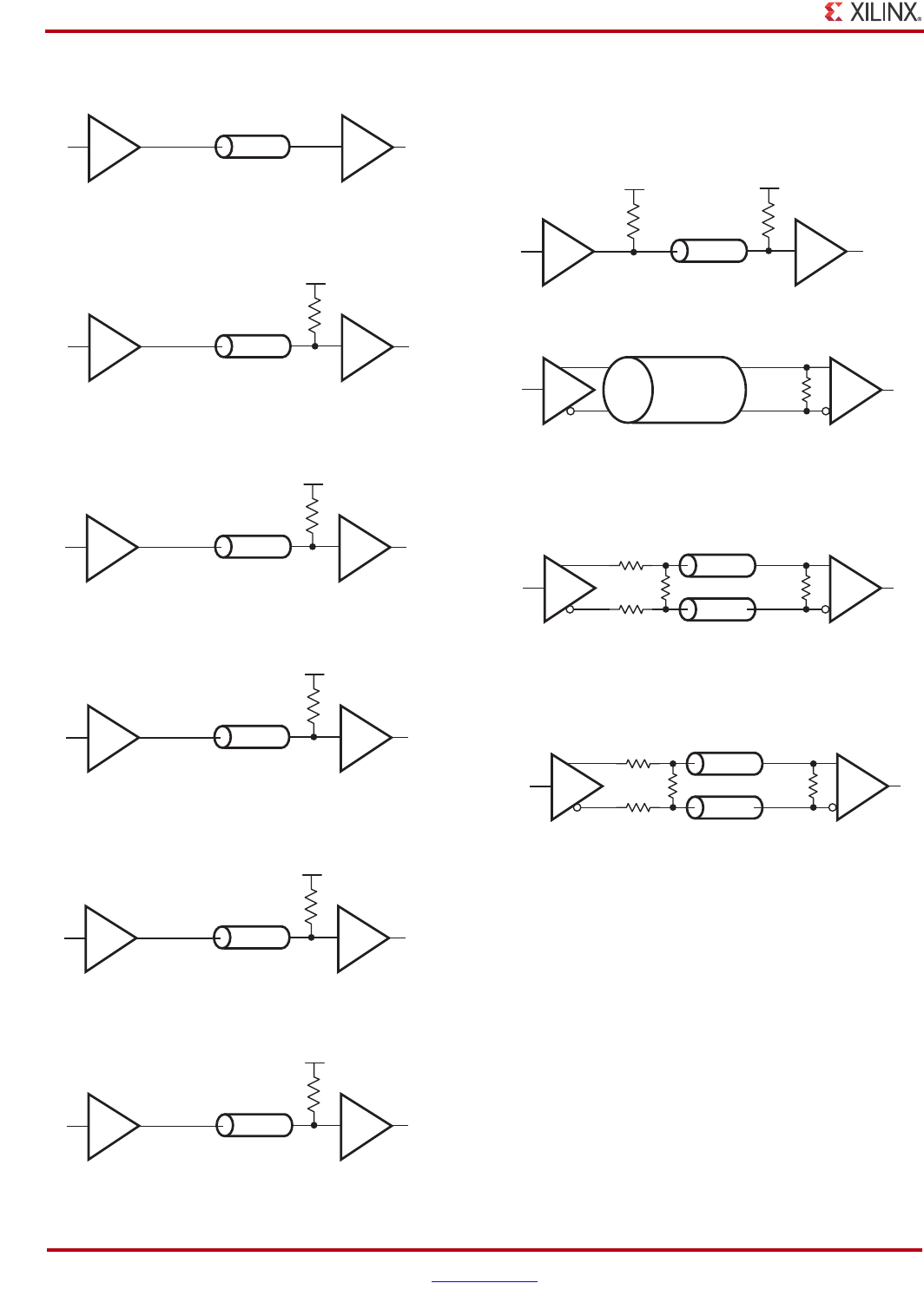
34 www.xilinx.com Spartan-6 FPGA SelectIO Resources
UG381 (v1.7) October 21, 2015
Chapter 1: SelectIO Resources
X-Ref Target - Figure 1-18
Figure 1-18: Example Terminations
ug381_c1_18_110210
Unterminated
Z=50
Z=50
50Far-end Parallel Termination to VCCO
FP_VCCO_50
V
CCO
50
1KFar-end Parallel Termination to VCCO
FP_VCCO_1000
V
CCO
Z=50
1K
Z=50
50Far-end Parallel Termination to 3.3V
FP_3.3_50
3.3V
50
1KFar-end Parallel Termination to 3.3V
FP_3.3_1000
3.3V
Z=50
1K
50Far-end Parallel Termination to VTT
FP_VTT_50
V
TT
= V
CCO
/2
Z=50
50
50Near-end Parallel Termination to VTT
50Far-end Parallel Termination to VTT
NP_VTT_50_FP_VTT_50
100Far-end Differential Termination
FD_100
V
TT
= V
CCO
/2
Z=50
50
100
V
TT
= V
CCO
/2
50
165Near Series, 140Near Differential,
100Far Differential
NS_165_ND_140_FD_100
Z=50
ZDIFF=100
100
140
165
165
Z=50
70Near Series, 187Near Differential,
100Far Differential
NS_70_ND_187_FD_100
Z=50
100
187
70
70
Z=50
Spartan-6 FPGA SelectIO Resources www.xilinx.com 35
UG381 (v1.7) October 21, 2015
SelectIO Signal Standards
Table 1-3 shows common example termination techniques for each of the SelectIO
standards available in the Spartan-6 FPGA SelectIO pins. Figure 1-18 gives a graphical
representation of each of these termination examples.
Table 1-3: Common Termination Examples by I/O Standard
I/O Standard Example Termination
BLVDS_25 NS_165_ND_140_FD_100
DIFF_HSTL_I, DIFF_HSTL_I_18 FP_VTT_50
DIFF_HSTL_II, DIFF_HSTL_II_18 NP_VTT_50_FP_VTT_50
DIFF_HSTL_III, DIFF_HSTL_III_18 FP_VCCO_50
DIFF_MOBILE_DDR None
DIFF_SSTL18_I, DIFF_SSTL2_I, DIFF_SSTL3_I FP_VTT_50
DIFF_SSTL15_II, DIFF_SSTL18_II, DIFF_SSTL2_II, DIFF_SSTL3_II NP_VTT_50_FP_VTT_50
DISPLAY_PORT None
HSTL_I, HSTL_I_18 FP_VTT_50
HSTL_II, HSTL_II_18 NP_VTT_50_FP_VTT_50
HSTL_III, HSTL_III_18 FP_VCCO_50
I2C FP_3.3_1000
LVCMOS12, LVCMOS15, LVCMOS18, LVCMOS25, LVCMOS33
(at 2mA, 4mA, 6mA, and 8mA)
None
LVCMOS12, LVCMOS15, LVCMOS18, LVCMOS25, LVCMOS33
(at 12mA, 16mA, and 24mA)
FP_VTT_50
LVDS_25, LVDS_33 FD_100
LVPECL_25, LVPECL_33 NS_70_ND_187_FD_100
LVTTL (at 2mA, 4mA, 6mA, and 8mA) None
LVTTL (at 12mA, 16mA, and 24mA) FP_VTT_50
MINI_LVDS_25, MINI_LVDS_33 FD_100
MOBILE_DDR None
PCI33_3, PCI66_3 None
PPDS_25, PPDS_33 FD_100
RSDS_25, RSDS_33 FD_100
SDIO FP_VCCO_1000
SMBUS FP_3.3_1000
SSTL18_I, SSTL2_I, SSTL3_I FP_VTT_50
SSTL15_II, SSTL18_II, SSTL2_II, SSTL3_II NP_VTT_50_FP_VTT_50
TMDS_33 FP_3.3_50
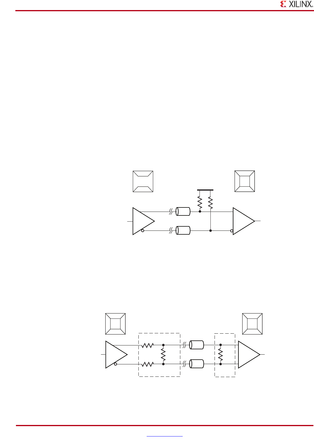
36 www.xilinx.com Spartan-6 FPGA SelectIO Resources
UG381 (v1.7) October 21, 2015
Chapter 1: SelectIO Resources
Differential I/O Standards
Differential standards employ a pair of signals, one the opposite polarity of the other. The
noise canceling properties (for example, common-mode rejection) of these standards
permit exceptionally high data-transfer rates.
Each device-package combination designates specific I/O pairs optimized to support
differential standards. When pin planning in the PlanAhead tool, differential pairs can be
seen in the Package window by looking at the unique internal name associated with each
package pin. The internal name, in IO_Lxx_x format, appears at the top of the circle
representing each I/O pin in the GUI. For each pair, the letters P and N designate the true
and inverted lines, respectively. For example, the internal names IO_L43P_3 and
IO_L43N_3 indicate the true and inverted lines comprising the line pair L43 on Bank 3.
TMDS_33 Termination
While many differential I/O standards use a simple 100Ω differential resistor at the
receiver, TMDS_33 does not. The TMDS_33 standard requires pull-up resistors as shown in
Figure 1-19.
BLVDS Output Termination
BLVDS outputs require external termination as shown in Figure 1-20. In the Spartan-6
FPGAs, the BLVDS outputs are allowed on any bank. There are no VCCO restrictions on
inputs, however, only VCCO = 2.5V is supported for outputs.
X-Ref Target - Figure 1-19
Figure 1-19: External Input Resistors Required for TMDS_33 I/O Standard
50Ω
VCCO = 3.3V
VCCAUX = 2.5V or 3.3V
VCCAUX = 3.3V
ug381_c1_29_121613DVI/HDMI cable
50Ω
3.3V
TMDS_33 TMDS_33
Bank 0
Bank 2
Bank 0 and 2
Bank 0
Bank 2
Bank 3
Bank 1
Any Bank
X-Ref Target - Figure 1-20
Figure 1-20: Spartan-6 FPGA External Output and Input Termination Resistors
for BLVDS I/Os
Z0 = 50Ω
Z0 = 50Ω
140Ω
165Ω
165Ω
100Ω
VCCO = 2.5V No VCCO Requirement
ug381_c1_30_051509
BLVDS_25 BLVDS_25
CAT16-LV4F12
Part Number
/ th of Bourns
14
CAT16-PT4F4
Part Number
/ th of Bourns
14
Bank 0
Bank 2
Bank 3
Bank 1
Any Bank
Bank 0
Bank 2
Bank 3
Bank 1
Any Bank
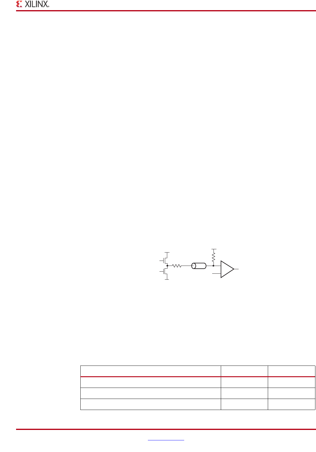
Spartan-6 FPGA SelectIO Resources www.xilinx.com 37
UG381 (v1.7) October 21, 2015
Supply Voltages for the IOBs
Supply Voltages for the IOBs
Depending on the actual user design, the IOBs can be powered by a combination of the
three primary FPGA supply rails: VCCINT, VCCO, and VCCAUX—and sometimes by the
dual-purpose VREF pins.
The VCCO supplies, one for each of the I/O banks, power the output drivers and some of
the input drivers. The voltage on the VCCO pins determines the voltage swing of the output
signal. All VCCO pins should be connected to supply rails on the board. If a bank is unused,
connect VCCO pins to an available VCCAUX or VCCO rail.
VCCINT is the main power supply for the internal FPGA logic. VCCINT also powers some of
the available input drivers.
VCCAUX is an auxiliary source of power used for various Spartan-6 FPGA functions,
including some of the I/O circuitry.
To meet full DC levels and be powered correctly, some of the input and output circuitry
requires VCCAUX to be constrained to the correct VCCAUX voltage level. The VCCAUX
voltage level can be set to either 2.5V or 3.3V. See the DC input and output level tables in
the Spartan-6 FPGA Data Sheet. The user constraint in the UCF that should be set to reflect
the planned VCCAUX level is:
CONFIG VCCAUX = “<2.5/3.3>”;
HSTL/SSTL VREF Reference Voltage
HSTL and SSTL inputs use the reference voltage (VREF) to bias the input-switching
threshold, as shown in Figure 1-21. Each input has an associated board termination voltage
(VTT).
The reference voltage VREF can be connected to multi-purpose VREF pins. All VREF inputs
on a bank must be connected to the same voltage. HSTL and SSTL inputs can only be
combined in a bank if they use the same VREF voltage (for example, the 1.8V versions of the
SSTL and HSTL standards, where VREF =0.9V.)
Because the VREF sets the switching levels, HSTL/SSTL inputs can be placed in any bank.
Table 1-4 lists the VREF and VTT values by I/O standard.
X-Ref Target - Figure 1-21
Figure 1-21: Terminated SSTL2 Class I
Table 1-4: VREF and VTT Values for I/O Standards
I/O Standard VREF VTT
HSTL_I 0.75 0.75
HSTL_II 0.75 0.75
HSTL_III 0.9 1.5
50Ω
Z = 50
SSTL2 Class I
ug381_c1_17_051209
25Ω
V
REF
= 1.25V
V
TT
= 1.25V
V
CCO
= 2.5V
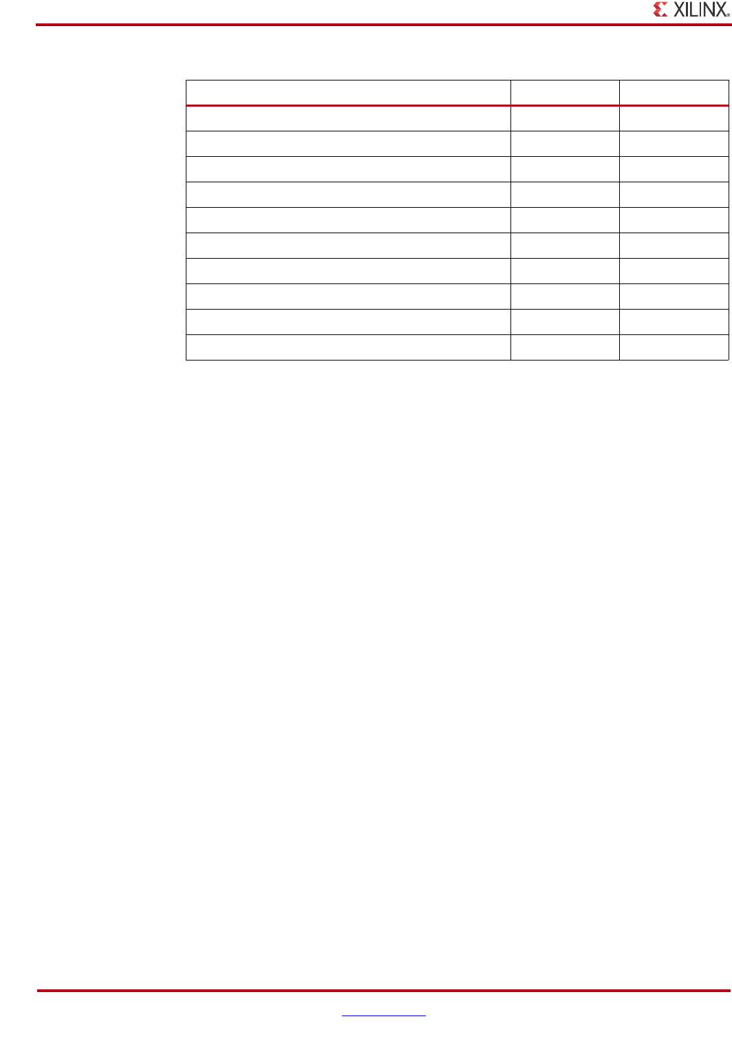
38 www.xilinx.com Spartan-6 FPGA SelectIO Resources
UG381 (v1.7) October 21, 2015
Chapter 1: SelectIO Resources
ESD Protection
The circuitry on Spartan-6 FPGA I/Os protects all device pads against damage from
electro-static discharge (ESD) as well as excessive voltage transients. ESD protection
specifications are typically for the Human Body Model. Details are provided in the
qualification/reliability report. In the Spartan-6 FPGAs, this protection circuitry does not
limit I/O voltage range.
I/O Standard Bank Compatibility
Spartan-6 FPGAs allow multiple I/O standards to be combined in the same device.
Although the outputs are always powered by VCCO, multiple standards are available
under one of the five possible VCCO values. In addition, inputs often do not need to match
the voltage applied to VCCO. Further flexibility is achieved with multiple VCCO levels in a
single device.
Each bank of I/Os has independent VCCO and VREF rails. This allows each bank to be
powered at VCCO and VREF levels independent of how the other banks are set. VCCO
provides power primarily to the I/O output buffers, and VREF supplies a reference voltage
for HSTL and SSTL inputs. The VCCO pins are dedicated power pins and must be powered
at all times with a voltage rail from the PCB. However, the VREF pins are dual-purpose
pins; they can be used as regular I/O pins or VREF-supply pins. When a bank uses
VREF-powered inputs (as an example, for the SSTL or HSTL standards), the design must
use the VREF pins to supply the FPGA’s internal VREF rail with the reference voltage. If the
SSTL or HSTL inputs are not used in a bank, the VREF pins in that bank can be used as
regular I/O pins. Table 1-5 lists the VCCO and VREF requirements.
HSTL_I_18 0.9 0.9
HSTL_II_18 0.9 0.9
HSTL_III_18 1.1 1.8
SSTL3_I 1.5 1.5
SSTL3_II 1.5 1.5
SSTL2_I 1.25 1.25
SSTL2_II 1.25 1.25
SSTL18_I 0.9 0.9
SSTL18_II 0.9 0.9
SSTL15_II 0.75 0.75
Table 1-4: VREF and VTT Values for I/O Standards (Cont’d)
I/O Standard VREF VTT
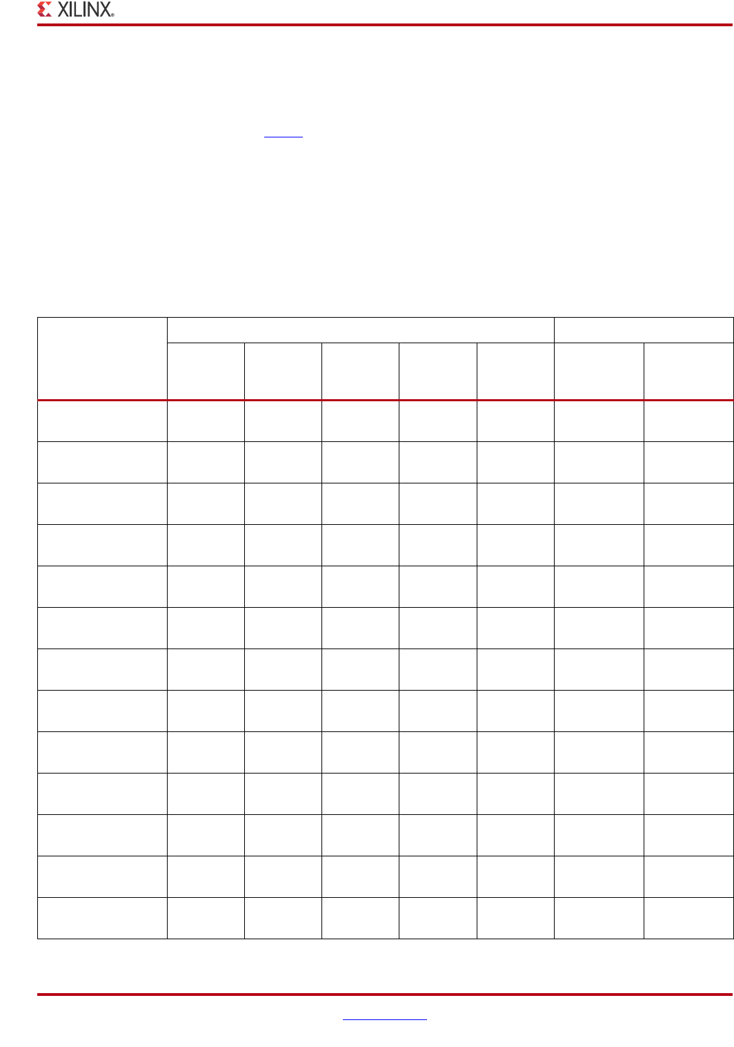
Spartan-6 FPGA SelectIO Resources www.xilinx.com 39
UG381 (v1.7) October 21, 2015
Supply Voltages for the IOBs
Single-Ended I/O Compatibility
For a particular VCCO voltage, Table 1-5 lists all of the single-ended I/O standards that can
either be combined, are only supported on the inputs, or can be used for both inputs and
outputs. See DS162: Spartan-6 FPGA Data Sheet for recommended operating conditions.
Table 1-2 lists the banking restrictions associated with LVCMOS drive strength. Table 1-5
also notes the single-ended outputs that are restricted to Banks 1, 3, 4, and 5 for the
following I/O standards:
•HSTL_II
•HSTL_II_18
• SSTL15_II
• SSTL18_II
Table 1-5: Spartan-6 FPGA Single-Ended I/O Standard Bank Compatibility
Single-Ended
I/O Standard
VCCO Supply and I/O Compatibility Input Voltage Requirements
1.2V 1.5V 1.8V 2.5V 3.3V VREF
Board
Termination
Voltage (VTT)
LVTTL Input Input Input Input Input/
Output
N/R(1) N/R
LVCMOS33 Input Input Input Input Input/
Output
N/R N/R
LVCMOS25 Input(2) Input(2) Input(2) Input/
Output
Input(2) N/R N/R
LVCMOS18 Input Input Input/
Output
Input Input N/R N/R
LVCMOS18_JEDEC N/A N/A Input/
Output
N/A N/A N/R N/R
LVCMOS15 Input Input/
Output
Input Input Input N/R N/R
LVCMOS15_JEDEC N/A Input/
Output
N/A N/A N/A N/R N/R
LVCMOS12 Input/
Output
Input Input Input Input N/R N/R
LVCMOS12_JEDEC Input/
Output
N/A N/A N/A N/A N/R N/R
PCI33_3/PCI66_3 N/A N/A N/A N/A Input/
Output
N/R N/R
I2C Input/
Output
Input/
Output
Input/
Output
Input/
Output
Input/
Output
N/R N/R
SMBus Input/
Output
Input/
Output
Input/
Output
Input/
Output
Input/
Output
N/R N/R
SDIO Input Input Input Input Input/
Output
N/R N/R
40 www.xilinx.com Spartan-6 FPGA SelectIO Resources
UG381 (v1.7) October 21, 2015
Chapter 1: SelectIO Resources
MOBILE_DDR N/A N/A Input/
Output
N/A N/A N/R N/R
HSTL_I Input Input/
Output
Input Input Input 0.75 0.75
HSTL_II(3) Input Input/
Output
Input Input Input 0.75 0.75
HSTL_III Input Input/
Output
Input Input Input 0.9 1.5
HSTL_I_18 Input Input Input/
Output
Input Input 0.9 0.9
HSTL_II_18(3) Input Input Input/
Output
Input Input 0.9 0.9
HSTL_III_18 Input Input Input/
Output
Input Input 1.1 1.8
SSTL3_I Input Input Input Input Input/
Output
1.5 1.5
SSTL3_II Input Input Input Input Input/
Output
1.5 1.5
SSTL2_I Input Input Input Input/
Output
Input 1.25 1.25
SSTL2_II Input Input Input Input/
Output
Input 1.25 1.25
SSTL18_I Input Input Input/
Output
Input Input 0.9 0.9
SSTL18_II(3) Input Input Input/
Output
Input Input 0.9 0.9
SSTL15_II(3) Input Input/
Output
Input Input Input 0.75 0.75
Notes:
1. N/R – Not required for input operation.
2. To use LVCMOS25 inputs when VCCO is not 2.5V, VCCAUX must be set to 2.5V.
3. Single-ended I/O outputs that are not available in Banks 0 and 2.
Table 1-5: Spartan-6 FPGA Single-Ended I/O Standard Bank Compatibility (Cont’d)
Single-Ended
I/O Standard
VCCO Supply and I/O Compatibility Input Voltage Requirements
1.2V 1.5V 1.8V 2.5V 3.3V VREF
Board
Termination
Voltage (VTT)
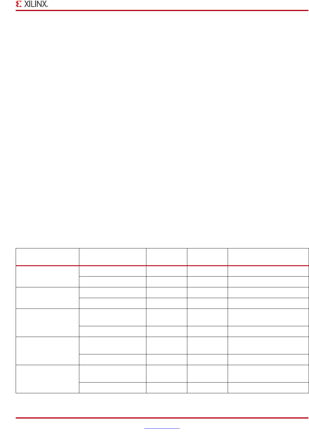
Spartan-6 FPGA SelectIO Resources www.xilinx.com 41
UG381 (v1.7) October 21, 2015
Supply Voltages for the IOBs
Differential I/O Standard Bank Compatibility
Many of the differential I/O standards can be combined within any given bank (see
Table 1-6). In Spartan-6 FPGAs, banks 0 and 2 can each support any two of the following
2.5V differential standards for output or bidirectional pins. There are no limits on pins that
are only used as inputs. The limitation of two is because each of these standards requires a
slightly different internal bias-voltage for the output buffer, which is provided from one of
two possible programmable bias-voltage generator circuits available in each bank:
•LVDS_25 outputs
• MINI_LVDS_25 outputs
•RSDS_25 outputs
• PPDS_25 outputs
Spartan-6 FPGA banks 0 and 2 alternatively support any two of the following 3.3V
differential outputs. The limitation of two is because each of these standards requires a
slightly different internal bias-voltage for the output buffer, which is provided from one of
two possible programmable bias-voltage generator circuits available in each bank:
•LVDS_33 outputs
• MINI_LVDS_33 outputs
•RSDS_33 outputs
• PPDS_33 outputs
•TMDS_33 outputs
As an example, LVDS_25 outputs, RSDS_25 outputs, and any other differential inputs are
a valid combination when using on-chip differential termination. An unsupported
combination is a single bank with LVDS_25 outputs, RSDS_25 outputs, and
MINI_LVDS_25 outputs. All the differential standards listed are only available as outputs
in banks 0 and 2, but any bank can have them as inputs as shown in Table 1-6.
Table 1-6: Differential I/O Standard Bank Compatibility
Differential
I/O Standard I/O Type VCCAUX VCCO Allowed Banks
BLVDS_25 Input 2.5/3.3 Any All
Output 2.5/3.3 2.5 All
DISPLAY_PORT
(AUXCH)
Input 2.5/3.3 Any All
Output 2.5/3.3 2.5 All
LVDS_25
Input or
Input with DIFF_TERM 2.5/3.3 Any All
Output 2.5/3.3 2.5 Bank 0, 2(1)
LVDS_33
Input or
Input with DIFF_TERM 2.5/3.3 Any All
Output 2.5/3.3 3.3 Bank 0, 2(1)
MINI_LVDS_25
Input or
Input with DIFF_TERM 2.5/3.3 Any All
Output 2.5/3.3 2.5 Bank 0, 2(1)
42 www.xilinx.com Spartan-6 FPGA SelectIO Resources
UG381 (v1.7) October 21, 2015
Chapter 1: SelectIO Resources
I/O Banking Rules
When assigning I/Os to banks, these VCCO rules must be followed:
•All V
CCO pins on the FPGA must be connected, even if a bank is unused.
MINI_LVDS_33
Input or
Input with DIFF_TERM 2.5/3.3 Any All
Output 2.5/3.3 3.3 Bank 0, 2(1)
RSDS_25
Input or
Input with DIFF_TERM 2.5/3.3 Any All
Output 2.5/3.3 2.5 Bank 0, 2(1)
RSDS_33
Input or
Input with DIFF_TERM 2.5/3.3 Any All
Output 2.5/3.3 3.3 Bank 0, 2(1)
PPDS_25
Input or
Input with DIFF_TERM 2.5/3.3 Any All
Output 2.5/3.3 2.5 Bank 0, 2(1)
PPDS_33
Input or
Input with DIFF_TERM 2.5/3.3 Any All
Output 2.5/3.3 3.3 Bank 0, 2(1)
LVPECL_25 Input 2.5/3.3 Any All
Output N/A N/A None
LVPECL_33 Input 3.3 Any All
Output N/A N/A None
TMDS_33 Input 3.3 Any All
Output 2.5/3.3 3.3 Bank 0, 2(1)
DIFF_HSTL_I/ I_18/
II/ II_18/ III/ III_18 Input/Output 2.5/3.3
Same as
single-ended
standards
Same as single-ended
standards
DIFF_SSTL_15/18/2/3 Input/Output 2.5/3.3
Same as
single-ended
standards
Same as single-ended
standards
DIFF_MOBILE_DDR Input/Output 2.5/3.3
Same as
single-ended
standards
Same as single-ended
standards
Notes:
1. Banks 0 and 2 can each support any two of the following 2.5V differential standards: LVDS_25 outputs, MINI_LVDS_25 outputs,
RSDS_25 outputs, PPDS_25 outputs, or any two of the following 3.3V differential standards: LVDS_33 outputs, MINI_LVDS_33
outputs, RSDS_33 outputs, PPDS_33 outputs, TMDS_33 outputs. Other I/O bank restrictions could also apply.
2. VREF is not used for these I/O standards.
Table 1-6: Differential I/O Standard Bank Compatibility (Cont’d)
Differential
I/O Standard I/O Type VCCAUX VCCO Allowed Banks

Spartan-6 FPGA SelectIO Resources www.xilinx.com 43
UG381 (v1.7) October 21, 2015
Supply Voltages for the IOBs
•All V
CCO lines associated within a bank must be set to the same voltage level.
•The V
CCO levels used by all standards assigned to the I/Os of any given bank must
agree. The Xilinx development software check for this.
• If a bank does not have VCCO requirements, connect VCCO to an available voltage,
such as 2.5V or 3.3V. Some configuration modes have additional VCCO requirements.
When a standard assigned to the inputs of a bank use VREF, then the following additional
rules must be followed:
•All V
REF pins must be connected within a bank.
•All V
REF lines associated with the bank must be set to the same voltage level.
•The V
REF levels used by all standards assigned to the inputs of the bank must agree.
The Xilinx development software check for this.
When VREF is not required to bias the input switching thresholds, all associated VREF pins
within the bank can be used as user I/Os or input pins.
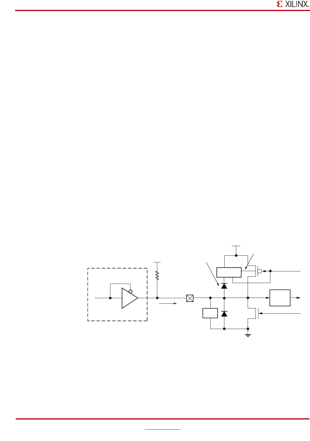
44 www.xilinx.com Spartan-6 FPGA SelectIO Resources
UG381 (v1.7) October 21, 2015
Chapter 1: SelectIO Resources
Using Large-Swing Signals
Independent of the I/O standard compatibility with VCCO, care must be taken to ensure
that VIN input voltages do not exceed the maximum specifications, which are sometimes
specified in relation to VCCO. For example, the Spartan-6 FPGA maximum VIN values are
independent of VCCO, except for the PCI standards (see Spartan-6 FPGA Data Sheet).
In some applications, the receive signals have a greater voltage swing than the I/Os
ordinarily permit. The most common case is receiving 5V signals on pins set to a 3.3V I/O
standard. These large-swing signals are by design or as a result of severe overshoot.
A similar situation can exist on the outputs, where the Spartan-6 FPGA needs to drive
external devices supporting standards with larger swing. The Spartan-6 FPGA outputs at
3.3V can directly drive most 5V devices, although with less margin. Similarly, the
LVCMOS25 dedicated configuration outputs can directly drive most 3.3V external devices.
This section describes potential options for interfacing to large-swing signals. In all cases,
designers must ensure that the specifications from the Spartan-6 FPGA Data Sheet are
heeded, particularly for VIN.
Voltage Translators
Xilinx recommends the use of voltage level translators when interfacing with large-swing
signals. A voltage level translator can be as simple as a two-resistor voltage divider, or as
complex as a PCI-to-PCI bridge.
Open-Drain Interfacing
The outputs of certain external devices can be configured as open-drain outputs. Outputs
with pull-up resistors tied to a low-voltage rail can be used to limit the signal swing and
not turn on the FPGA power diode (see Figure 1-22).
X-Ref Target - Figure 1-22
Figure 1-22: A 3.3V Open-Drain Output Connected to a Dedicated FPGA Input
VOH
IOH
Open-Drain
3.3V µP
VCCAUX = 2.5V
VCCO
Input
UG381_c1_31_111609
Well Bias
Floating N-Well
N
–
V
DG
+
PCI
Clamp
ESD
P
Input
Buffer

Spartan-6 FPGA SelectIO Resources www.xilinx.com 45
UG381 (v1.7) October 21, 2015
Supply Voltages for the IOBs
I/O Pins During Power-On and Configuration
In this section, all behavior described for I/O pins also applies to dual-purpose I/O pins
that are not actively involved in the currently selected configuration mode.
The VCCINT (1.2V), VCCAUX, and VCCO supplies can be applied in any order. Before the
FPGA starts the configuration process, VCCINT, VCCO Bank 2 and VCCAUX must have
reached their respective minimum recommended operating levels indicated in the data
sheet. At this time, all output drivers are in a high-impedance state. VCCO Bank 2, VCCINT,
and VCCAUX serve as inputs to the internal power-on reset (POR) circuit.
The HSWAPEN pin controls the internal pull-up resistors on all of the user I/O pins from
power-on through completion of configuration. A Low level applied to the HSWAPEN pin
during configuration enables the internal pull-up resistors, while a High level disables
them. The HSWAPEN pin itself contains an internal pull-up resistor that is present through
the completion of configuration and defaults to High when left floating on the board.
Therefore, to enable the internal pull-up resistors on the user I/O pins prior to completion
of configuration, the HSWAPEN pin must be either connected directly to GND, or forced
Low by another device on the board.
As soon as power is applied, the FPGA begins initializing its configuration memory. At the
same time, the FPGA internally asserts the global set-reset (GSR) to asynchronously resets
all IOB storage elements to a default Low state.
Upon the completion of initialization and the beginning of configuration, INIT_B
transitions High, sampling the M0 and M1 inputs to determine the configuration mode.
Configuration data is then loaded into the FPGA. The I/O drivers remain in a high-
impedance state (with or without pull-up resistors, as determined by the HSWAPEN
input) throughout configuration.
At the end of configuration, the GSR net is released, placing the IOB registers in a Low state
by default, unless the loaded design reverses the polarity of their respective SR inputs.
The global 3-state (GTS) net is released during start-up, marking the end of configuration
and the beginning of design operation in the User mode. After the GTS net is released, all
user I/Os transition active while all unused I/Os are pulled down (PULLDOWN). The
designer can control termination on the unused I/Os after GTS is released by setting the
unused pin bitstream generator (BitGen) option to PULLUP, PULLDOWN, or FLOAT.
One clock cycle later (default), the global write enable (GWE) net is released allowing the
RAM and registers to change states. Once in User mode, any pull-up resistors enabled by
HSWAPEN revert to the user settings and HSWAPEN is available as a general-purpose
I/O pin.
For more information on the power-up and configuration processes, see the Spartan-6
FPGA Configuration User Guide.
Unused I/O Pins After Configuration
By default, the Xilinx ISE development tools automatically configure all unused I/O pins
as input pins with individual internal pull-down resistors to GND.
This default behavior is controlled by the UnusedPin BitGen option.

46 www.xilinx.com Spartan-6 FPGA SelectIO Resources
UG381 (v1.7) October 21, 2015
Chapter 1: SelectIO Resources
Driving Unpowered I/O Banks
In some cases, one or more I/O banks in an FPGA are not used (for example, when an
FPGA has far more I/O pins than the design requires). In these cases, it might be desirable
to leave the bank’s associated VCCO pins unconnected to free up some PCB layout
constraints (less voiding of power and ground planes from antipads, fewer obstacles to
signals entering and exiting the pinout array, and more copper area available for other
planelets in the otherwise-used plane layer).
Leaving the VCCO pins of unused I/O banks floating reduces the level of ESD protection
on these pins and the I/O pins in the bank. For maximum ESD protection in an unused
bank, all VCCO and I/O pins in that bank should be connected together to the same
potential, whether that be ground, a valid VCCO voltage, or a floating plane.

Spartan-6 FPGA SelectIO Resources www.xilinx.com 47
UG381 (v1.7) October 21, 2015
Chapter 2
SelectIO Logic Resources
Introduction
This chapter describes the logic before the I/O drivers and after the receivers covered in
Chapter 1, SelectIO Resources.
Spartan®-6 FPGAs contain all of the basic I/O logic resources from previous Spartan
FPGAs. These resources include the following:
• Combinatorial input/output
• 3-state output control
• Registered input/output
• Registered 3-state output control
• Double Data Rate (DDR) input/output
• DDR output 3-state control
In addition, Spartan-6 FPGAs implement these advanced architectural features:
• IODELAY2 provides user control of an adjustable, fine-resolution delay primitive
• NONE, C0, and C1 output DDR mode
• NONE, C0, and C1 input DDR mode
• ISERDES discussed in Chapter 3, Advanced SelectIO Logic Resources.
• OSERDES discussed in Chapter 3, Advanced SelectIO Logic Resources.
A design checklist is provided in UG393, Spartan-6 FPGA PCB Design Guide to assist with
pin planning.
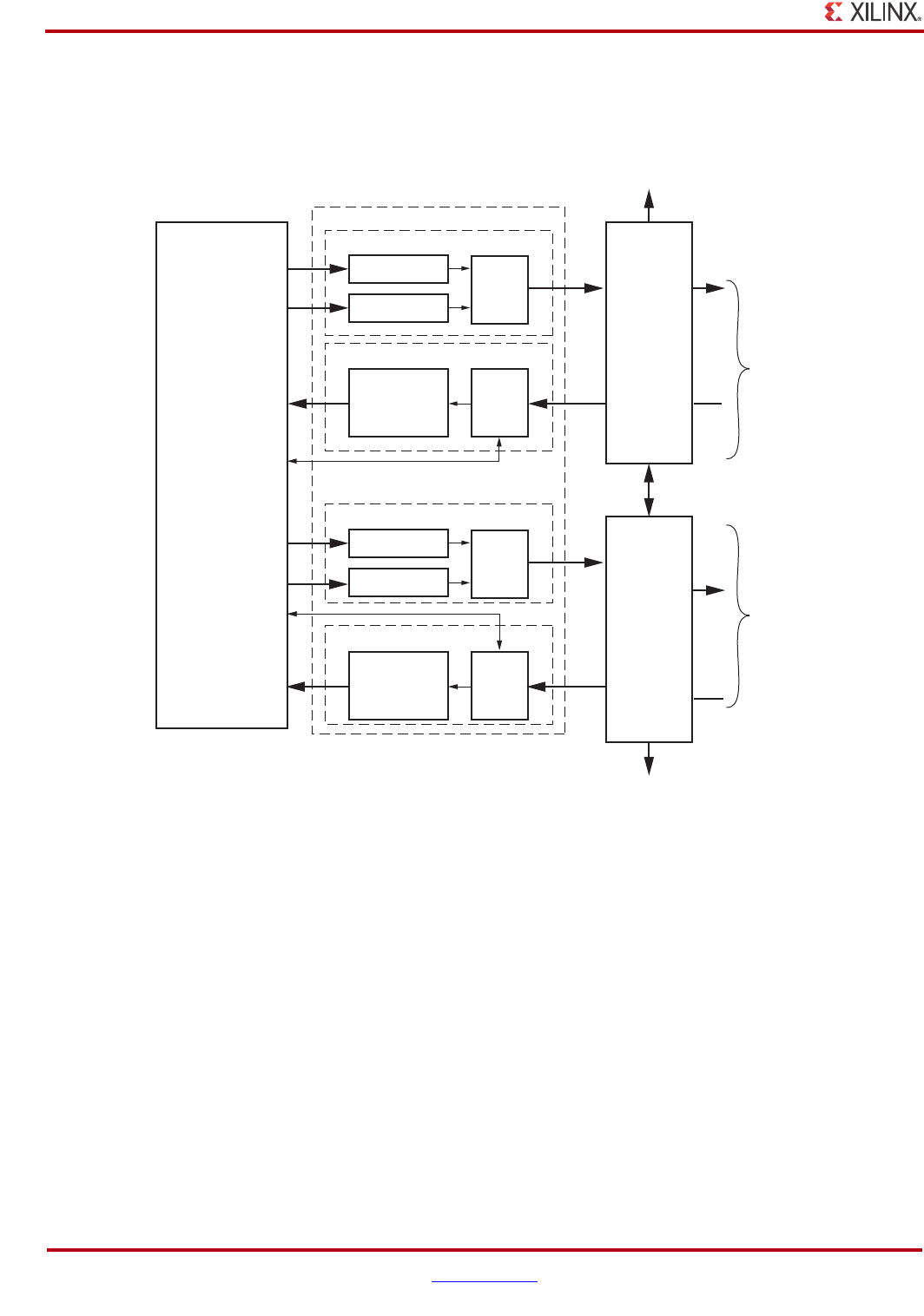
48 www.xilinx.com Spartan-6 FPGA SelectIO Resources
UG381 (v1.7) October 21, 2015
Chapter 2: SelectIO Logic Resources
I/O Interface Tile
All Spartan-6 FPGA SelectIO™ resources are grouped into an I/O interface tile as shown in
Figure 2-1.
Each I/O interface logic (IOI) tile manages two I/O buffers (IOBs) which actually drive or
receive signals from the device pins. Each IOI contains the complete circuitry for two
single-ended input/outputs or one differential input or output, and an interconnect block.
The two IOBs are combined in the IOI to provide additional functionality when supporting
high-speed differential interface standards.
In single-ended mode, the master I/O buffer drives the pad (P) and the slave I/O buffer
drives the pad (N). In differential mode, the resources in the master and slave I/O buffers
are combined and can create a parallel-to-serial or serial-to-parallel conversion with a rate
of up to twice that of a single I/O buffer. The master I/O logic cascades into the slave I/O
logic and the data is output LSB first where the LSBs are written into the slave block.
Each I/O interface tile contains the circuitry needed to support asynchronous I/O, latched
I/O, registered I/O, or a 2:1/3:1/4:1 cascadable SerDes (see Chapter 3, Advanced SelectIO
Logic Resources). The I/O interface tile input cell’s SDR flip-flop/latch has an SR input
allowing either set or reset functionality. All other flip-flops have an asynchronous reset
only.
X-Ref Target - Figure 2-1
Figure 2-1: SelectIO Logic Resources within the I/O Input Tile
Master OLOGIC
IOI Tile
Serializer (T)
Serializer (D)
Master ILOGIC
De-serializer
odelay
idelay
Slave OLOGIC
Serializer (T)
Serializer (D)
Slave ILOGIC
De-serializer
odelay
idelay
Master
IOB (P)
Slave
IOB (N)
High
Speed
I/O Clocks
High
Speed
I/O Clocks
UG381_c2_01_022310
FPGA
Interconnect
Logic

Spartan-6 FPGA SelectIO Resources www.xilinx.com 49
UG381 (v1.7) October 21, 2015
Clock Resources Available to the I/O Interface Logic
Prior to global-write-enable, all flip-flops/latches are reset to 0 (output in High-Z). All flip-
flops are positive-edge triggered only.
The latching/registering clock can come from either the global clock (GCLK) network or
the high-speed I/O clock network (see Spartan-6 FPGA Clocking Resources). Typically, the
GCLK signals output data at slow to moderate output rates below the global clock network
frequency limitation (See Spartan-6 FPGA Data Sheet).
The IODELAY primitives are optionally added to the input and output paths. The amount
of delay is programmable using the IODELAY2 primitive. Delays can be fixed or variable.
See Chapter 1, SelectIO Resources. Typical delays are specified in the Spartan-6 FPGA Data
Sheet.
Clock Resources Available to the I/O Interface Logic
The clock resources available to the SelectIO logic are shown in Figure 2-2. All I/O data
sampling and data transmission is performed with an internal SDR clock, both for receive
and transmit, even when the external data is DDR with respect to the received clock. To
achieve this, each I/O interface tile contains a local frequency doubler, which can be used
to obtain the necessary SDR sampling or transmitter clock.
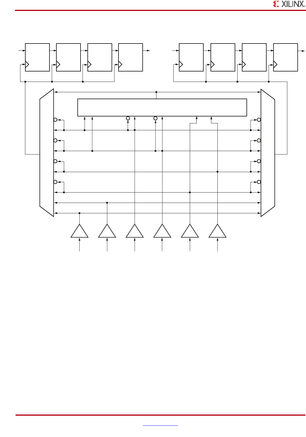
50 www.xilinx.com Spartan-6 FPGA SelectIO Resources
UG381 (v1.7) October 21, 2015
Chapter 2: SelectIO Logic Resources
The frequency doubler, which must be used for sampling or transmission of DDR data,
requires two clock inputs to operate. These two inputs can be either:
• A global clock and its complement via local inversion
• Two global clocks 180° apart
• Two I/O clocks 180° apart
The doubler can not accept mixed signals, such as one global clock and one I/O clock.
There is only one doubler per I/O interface logic block, and once the doubler is enabled
then its input clock signals are no longer available for use. This has implications for
bidirectional I/O capability, which is shown in Table 2-1, and also for clock feedback
connectivity. Specifically, when an external clock input is feeding DDR registers in its
corresponding ILOGIC block, then the use of the doubler (required for DDR) removes the
possibility of feeding either of the two original clocks (coming from a DCM) back to the
DCM through a BUFIO2FB. In this case the feedback to the DCM will need to come directly
from a global buffer.
X-Ref Target - Figure 2-2
Figure 2-2: IOI Interface Logic Clocking Resources
Clock Doubler (Clock Input Pairs)
BUFPLL BUFPLL BUFG BUFG BUFIO2 BUFIO2
Samping
FF
IDDR2/
2nd
ISERDES
FF
3rd
ISERDES
FF
4th
ISERDES
FF
4th
OSERDES
FF
3rd
OSERDES
FF
ODDR2/
2nd
OSERDES
FF
Output
FF
Data Out
to Pin
Data In From Pin
(input delay not shown)
Output
Logic Clock
Multiplexer
Input
Logic
Clock
Multiplexer
ug381_c2_02new_011109
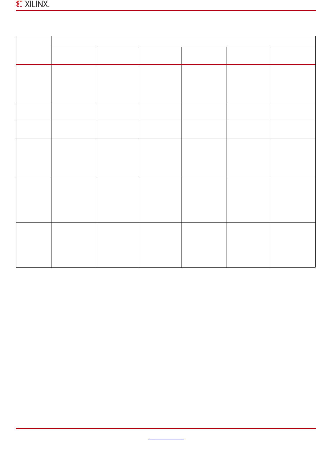
Spartan-6 FPGA SelectIO Resources www.xilinx.com 51
UG381 (v1.7) October 21, 2015
Clock Resources Available to the I/O Interface Logic
The I/O logic clocking structure has access to two clocks coming from global buffers. These
can be used as either true or inverted clocks (with SDR signals), or as inputs to the local
frequency doubler to generate the local SDR sampling or as the transmission clock
required for use with DDR signals. A global clock can feed I/O on all banks of the device
simultaneously.
The I/O logic clocking structure also has access to two clocks coming from a PLL using the
BUFPLL. These clocks are always SDR internally, and are not invertible. In the case of
external DDR signals, the received clock is multiplied by two in the PLL. PLL clock signals
are never used by the doubler. These clock inputs are never invertible when being used
with a SerDes as inversion invalidates the timing to the I/O strobe signals also coming
from the BUFPLL. Clocks from a BUFPLL can drive I/O across one whole edge of the
device, there are two BUFPLLs per edge.
The I/O logic clocking structure also has access to two clocks coming from BUFIO2 I/O
clocks. These can be used as either true or inverted clocks for use with external SDR signals
or as inputs to the local frequency doubler to generate the local SDR sampling or as a
transmission clock required for use with external DDR signals. The BUFIO2s must be in
the same half side of the device as the data pin being clocked. These clock inputs are not
Table 2-1: Possible Clock Structures for Bidirectional I/O
Output
Input
SDR BUFPLL
Clock
SDR Single
BUFG
SDR Single
BUFIO2
DDR Single
BUFG
DDR Two
BUFGs
DDR Two
BUFIO2s
SDR
BUFPLL
Clock
Only possible
when the BUFG
is common for
both input and
output
Possible Possible Possible
Only possible
when two
BUFGs are
used in the I/O
logic
Possible
SDR Single
BUFG Possible Possible Possible Not Possible Not Possible Not Possible
SDR Single
BUFIO2 Possible Possible Possible Not Possible Not Possible Not Possible
DDR Single
BUFG Possible Not Possible Not Possible
Only possible
when the BUFG
is common for
both input and
output
Not Possible Not Possible
DDR Two
BUFGs
Only possible
when the two
BUFGs are
used in the I/O
logic
Not Possible Not Possible Not Possible
Only possible
when the two
BUFGs are
common for
both input and
output
Not Possible
DDR Two
BUFIO2s Possible Not Possible Not Possible Not Possible Not Possible
Only possible
when the two
BUFIO2s are
common for
both input and
output
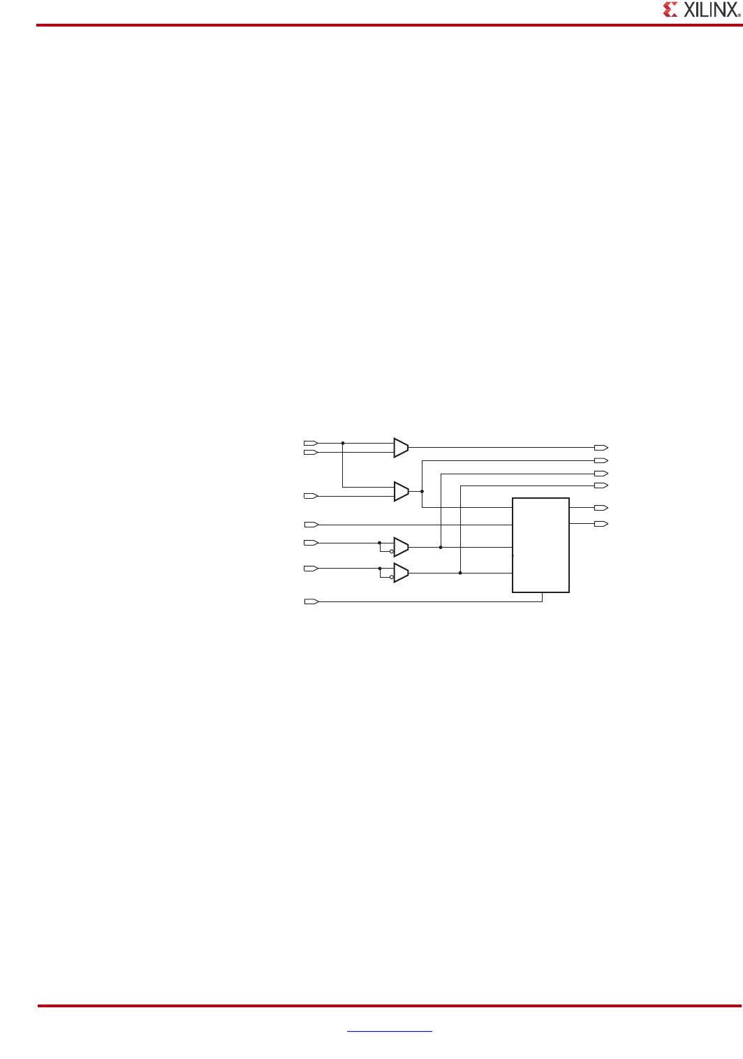
52 www.xilinx.com Spartan-6 FPGA SelectIO Resources
UG381 (v1.7) October 21, 2015
Chapter 2: SelectIO Logic Resources
invertible when being used with the doubler, or with a SerDes as inversion invalidates the
timing to the I/O strobe signals also coming from the BUFIO2.
An incoming DDR I/O clock must be routed using two BUFIO2 clock buffers to generate
the required true and complement clocks for the frequency doubler. Typically, the
incoming clock uses two zero-delay IODELAY2 primitives to balance data delays. With
differential clock signalling this balance is not an issue. With single-ended clock signals,
the clock signal needs to be input to the FPGA through two separate clock input pins, with
one configured to invert the clock signal for access the two IODELAY2 primitives and the
two BUFIO2 clocks.
When using a SerDes in the input or output path with either BUFIO2 or BUFPLL clocking,
a global clock is required to get data to or from the SerDes. Using this global buffer can
limit the clocking capabilities available in certain bidirectional I/O configurations, as only
two global clocks can enter the I/O logic.
The matrix in Table 2-1 shows the clocking structures that can be mixed for input and
output logic in bidirectional I/O.
ILOGIC2 Resources
The ILOGIC2 primitive block diagram is shown in Figure 2-3.
X-Ref Target - Figure 2-3
Figure 2-3: ILOGIC2 Block Diagram
DDLY2
DDLY
D
DQ0
Q1
Q0
DFB
CFB0
CFB1
FABRICOUT
Q1
CE
C0
SR
CE
C0
SR
ug381_c2_02_051109
C1
C1
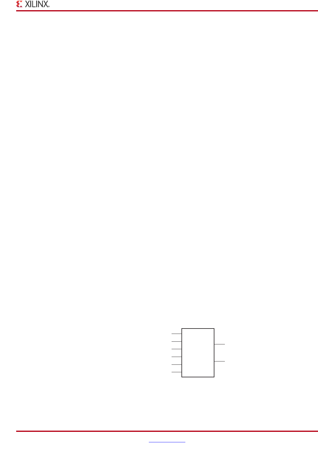
Spartan-6 FPGA SelectIO Resources www.xilinx.com 53
UG381 (v1.7) October 21, 2015
ILOGIC2 Resources
ILOGIC2 can support the following operations:
• Edge-triggered D-type flip-flop
• IDDR2 mode (NONE, C0, or C1). See Input DDR Primitive, for further discussion of
input DDR.
• Level sensitive latch
• Asynchronous/combinatorial
ILOGIC2 has one data input D from a corresponding IOB, clock inputs C0 and C1 (always
with a 180° phase difference), and one common shared clock enable CE0 that defaults to
the active state when it is unconnected. ILOGIC2 has one SR pin configurable as either SET
or RESET which can be either synchronous or asynchronous. When asynchronous, RESET
can be applied asynchronously but must be deasserted synchronously. ILOGIC2 also
accepts delayed data DDLY and DDLY2 from IODELAY2 (see I/O Delay Overview).
On the output, FABRICOUT is used to route through either D or DDLY2. Q0 and Q1 are the
ILOGIC2 register outputs. There are also dedicated clock output pins DFB for routing
through a clock input to a BUFIO2 and CFB0/CFB1 to pass clock inputs to BUFIO2FB. See
Spartan-6 FPGA Clocking Resources.
The following sections discuss the various ILOGIC2 resources. All connections between
the ILOGIC2 resources are managed using Xilinx software.
Combinatorial Input Path
The combinatorial input path creates a direct connection from the input driver to the FPGA
logic. This path is used by software automatically when:
• There is a direct (unregistered) connection from input data to logic resources in the
FPGA.
• The “pack I/O register/latches into IOBs” attribute is set to OFF.
Input DDR Primitive
ILOGIC2 has dedicated DDR registers, accessible when the IDDR2 primitive is
instantiated.
IDDR2 Primitive
Figure 2-4 shows the block diagram of the IDDR2 primitive. Table 2-2 lists the IDDR2
primitive ports. Table 2-3 describes the port attributes and default values for the IDDR2
primitive.
X-Ref Target - Figure 2-4
Figure 2-4: IDDR2 Primitive Block Diagram
ug381_c2_03_031709
D
CE
Q0
Q1
IDDR2
C1
C0
R
S
54 www.xilinx.com Spartan-6 FPGA SelectIO Resources
UG381 (v1.7) October 21, 2015
Chapter 2: SelectIO Logic Resources
The IDDR2 registers the incoming data to Q0 using the rising edge of C0, and the incoming
data to Q1 using the rising edge of C1, which is typically the same as the falling edge of C0.
This data is then transferred into the FPGA logic. Figure 2-5 shows the implementation
and timing for an input DDR in NONE mode.
Table 2-2: IDDR2 Port Signals
Port Name Function Description
D Input Data input
C0 Input Clock input, optionally invertible
C1 Input Second clock input having 180° phase difference relative to C0,
optionally invertible
CE Input Clock enable
R Input Reset. Software will issue an error if both R and S are connected
S Input Set. Software will issue an error if both R and S are connected
Q0 and Q1 Output Data outputs
Table 2-3: IDDR2 Attribute Summary
Attribute Name Possible
Values Default Value Description
DDR_ALIGNMENT NONE,
C0, or C1
NONE Set DDR output alignment mode.
When used bidirectionally, the
mode must agree with the
corresponding ODDR2 mode.
INIT_Q0 0 or 1 0 Q0 initialization value. Software
will issue an error if INIT_Q0 and
INIT_Q1 are not the same.
INIT_Q1 0 or 1 0 Q1 initialization value. Software
will issue an error if INIT_Q0 and
INIT_Q1 are not the same.
SRTYPE ASYNC or
SYNC
SYNC Set/Reset synchronization type.
ASYNC is valid for all modes,
SYNC is only available for NONE
mode. When asynchronous,
RESET can be applied
asynchronously but must be
deasserted synchronously.
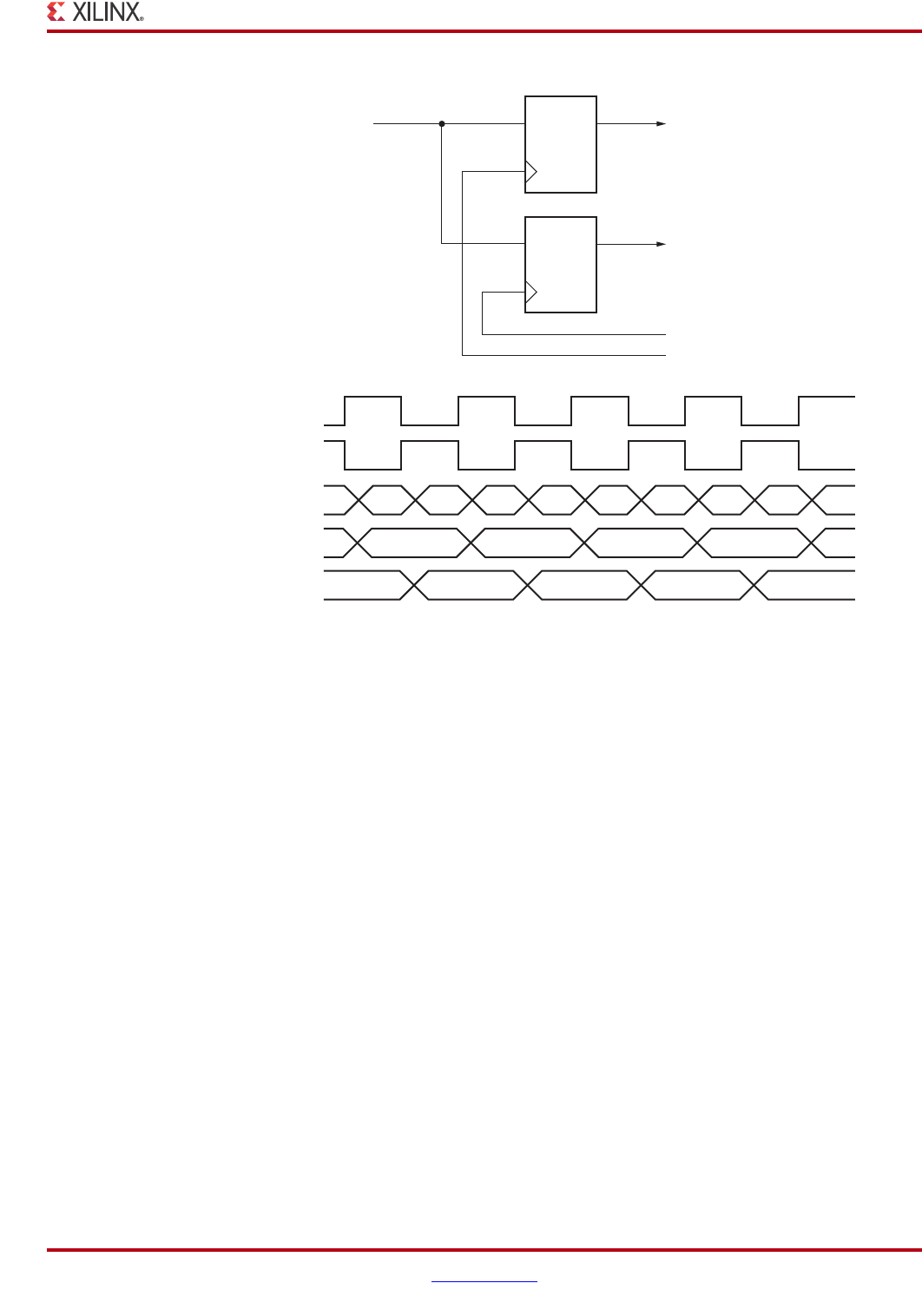
Spartan-6 FPGA SelectIO Resources www.xilinx.com 55
UG381 (v1.7) October 21, 2015
ILOGIC2 Resources
At some point in a design, both signals must be brought into the same clock domain,
typically C0. This can be difficult at high frequencies because the available time is only one
half of a clock cycle assuming a 50% duty cycle. The IDDR2 contains dedicated paths to
allow this clock domain transition to occur inside the ILOGIC2 block.
X-Ref Target - Figure 2-5
Figure 2-5: Input DDR when DDR_ALIGNMENT = NONE
D
DQ0Q
DQ1
To FPGA
Logic
C1
C0
C0
C1
D
Q0
d + 1d
d + 2 d + 4 d + 6 d + 8
d
d + 2 d + 3d + 4 d + 5 d + 6 d + 7 d + 8
Q
Q1 d + 3d – 1 d + 5 d + 7d + 1
UG381_c2_04_102210
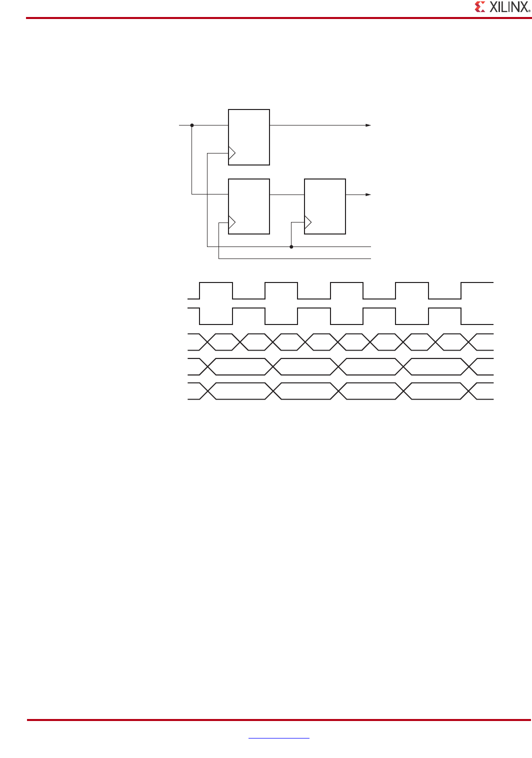
56 www.xilinx.com Spartan-6 FPGA SelectIO Resources
UG381 (v1.7) October 21, 2015
Chapter 2: SelectIO Logic Resources
When DDR_ALIGNMENT = C0 (or C1), the signal Q1 (Q0) is re-registered to C0 (C1), and
is only then fed to the interconnect CLB logic keeping the outputs in the same clock
domain. Figure 2-6 illustrates how the interconnecting logic uses only the clock C0 to
forward the received data.
X-Ref Target - Figure 2-6
Figure 2-6: Input DDR When DDR_ALIGNMENT = C0
DQ0DQ
DQ1
To FPGA
Logic
C0
C1
C0
C1
D
Q0
d + 1d
d + 2 d + 4 d + 6 d + 8
d
d + 2 d + 3d + 4 d + 5 d + 6 d + 7 d + 8
QDQ
Q1 d + 3d – 1 d + 5 d + 7
d + 1
UG381_c2_05_102110
Spartan-6 FPGA SelectIO Resources www.xilinx.com 57
UG381 (v1.7) October 21, 2015
ILOGIC2 Resources
Figure 2-7 illustrates how the interconnecting logic uses only the clock C1 to forward the
received data.
IDDR2 VHDL and Verilog Templates
The Libraries Guide includes templates for instantiation of the IDDR2 primitive in VHDL
and Verilog.
ILOGIC2 Timing Models
This section describes the timing associated with the various resources within the ILOGIC2
block.
X-Ref Target - Figure 2-7
Figure 2-7: Input DDR When DDR_ALIGNMENT = C1
C0
C1
D
Q0
d + 1
d – 1 d
d + 2 d + 4 d + 6d
d + 2 d + 3d + 4 d + 5 d + 6 d + 7 d + 8
Q1 d + 3d – 1 d + 5d + 1
UG381_c2_07_111910
DQ0DQ
DQ1
To FPGA
Logic
C1
C0
QDQ
58 www.xilinx.com Spartan-6 FPGA SelectIO Resources
UG381 (v1.7) October 21, 2015
Chapter 2: SelectIO Logic Resources
ILOGIC2 Timing Characteristics
Figure 2-8 illustrates ILOGIC2 register timing. When IDELAY is used, TIDOCK is replaced
by TIDOCKD.
Clock Event 1
At time TICECK before Clock Event 1, the input clock enable signal becomes valid-high at
the CE input of the input register, enabling the input register for incoming data.
At time TIDOCK before Clock Event 1, the input signal becomes valid-high at the D input of
the input register and is reflected on the Q output of the input register at time TICKQ after
Clock Event 1.
Clock Event 4
At time TISRCK before Clock Event 4, the SR signal (configured as synchronous reset in this
case) becomes valid-high resetting the input register and reflected at the Q output of the
IOB at time TICKQ after Clock Event 4.
ILOGIC2 Timing Characteristics, DDR
Figure 2-9 illustrates the ILOGIC2 in IDDR2 mode timing characteristics. When IDELAY is
used, TIDOCK is replaced by TIDOCKD. The example shown uses IDDR2 in
DDR_ALIGNMENT = NONE mode. For other modes (C0 or C1), the timing description
remains the same, but both Q0 and Q1 are output synchronous to either C0 or C1.
X-Ref Target - Figure 2-8
Figure 2-8: ILOGIC2 Input Register Timing Characteristics
12345
CLK
D
CE
SR
Q
TICKQ TICKQ
TIDOCK
TICECK
TISRCK
ug381_c2_06_061209
Spartan-6 FPGA SelectIO Resources www.xilinx.com 59
UG381 (v1.7) October 21, 2015
ILOGIC2 Resources
Clock Event 1
At time TICECK before Clock Event 1, the input clock enable signal becomes valid-high at
the CE input of both of the DDR input registers, enabling them for incoming data. Since the
CE and D signals are common to both DDR registers, care must be taken to toggle these
signals between the rising edges and falling edges of C0 as well as meeting the register
setup-time relative to both clocks.
At time TIDOCK before Clock Event 1 (rising edge of C0), the input signal becomes valid-
high at the D input of both registers and is reflected on the Q0 output of input-register 1 at
time TICKQ after Clock Event 1.
Clock Event 2
At time TIDOCK before Clock Event 2 (rising edge of C1), the input signal becomes valid-
low at the D input of both registers and is reflected on the Q1 output of input-register 2 at
time TICKQ after Clock Event 2 (no change in this case).
Clock Event 9
At time TISRCK before Clock Event 9, the R signal (configured as synchronous reset in this
case) becomes valid-high resetting Q0 at time TICKQ after Clock Event 9, and Q1 at time
TICKQ after Clock Event 10.
X-Ref Target - Figure 2-9
Figure 2-9: ILOGIC2 in IDDR2 Mode Timing Characteristics
1234567891011
TIDOCK
TICECK
TISRCK
TICKQ
TICKQ
TICKQ
TIDOCK
C0
C1
D
CE
R
(Reset)
Q0
Q1
TICKQ
UG381_c2_07_0061209
60 www.xilinx.com Spartan-6 FPGA SelectIO Resources
UG381 (v1.7) October 21, 2015
Chapter 2: SelectIO Logic Resources
Table 2-4 describes the function and control signals of the ILOGIC2 switching
characteristics in the Spartan-6 FPGA Data Sheet.
Note: The DDLY timing diagrams and parameters are identical to the D timing diagrams and
parameters.
OLOGIC2 Resources
The OLOGIC2 primitive consists of two major blocks, one to configure the output data
path and the other to configure the 3-state control path. Figure 2-10 shows the block
diagram.
The output and the 3-state paths can be independently configured in one of the following
modes:
• Edge-triggered D-type flip-flop
• DDR (NONE, C0, or C1 alignment mode)
• Level sensitive latch
• Asynchronous/combinatorial
Table 2-4: ILOGIC2 Switching Characteristics
Symbol Description
Setup/Hold
TICECK/TICKCE CE pin Setup/Hold with respect to CLK
TISRCK/TICKSR SR pin Setup/Hold with respect to CLK
TIDOCK/TIOCKD D pin Setup/Hold with respect to CLK
Combinatorial
TIDI D pin to O pin propagation delay, no Delay
Sequential Delays
TIDLO D pin to Q0 pin using flip-flop as a latch without Delay
TICKQ CLK to Q outputs
TICEQ CE pin to Q0 using flip-flop as a latch, propagation delay
TRQ SR pin to Q out
Spartan-6 FPGA SelectIO Resources www.xilinx.com 61
UG381 (v1.7) October 21, 2015
OLOGIC2 Resources
An OLOGIC2 block typically has two data inputs D0 and D1 from logic interconnect, two
clock inputs C0 and C1 (often 180° off in phase), and one common shared clock enable CE
that defaults to active state when unconnected.
OLOGIC2 has one SR pin that can be configured into either SET or RESET and can be either
synchronous or asynchronous. All connections between the OLOGIC2 resources are
managed by Xilinx software.
Combinatorial Output Data and 3-State Control Path
The combinatorial output paths create a direct connection from the interconnect logic to
the output driver or output driver control. These paths are used when:
• There is direct (unregistered) connection from logic resources in the interconnect logic
to the output data or 3-state control.
• The “pack I/O register/latches into IOBs” is set to OFF.
Output DDR Overview (ODDR2)
OLOGIC2 has dedicated DDR registers, accessible when the ODDR2 primitive is
instantiated. DDR multiplexing is automatic when using OLOGIC2. MUX-select control is
generated from the clock, and no manual control is needed. Each ODDR2 register has two
clock inputs, usually 180° out of phase.
Note: When an ODDR2 primitive is used in conjunction with a 3-state output, the T control pin must
also use an ODDR2 primitive configured in the same mode as the ODDR2 primitive used for data
output.
X-Ref Target - Figure 2-10
Figure 2-10: OLOGIC2 Block Diagram
D
CE
FF/LATCH
SR
QQ
D0
D1
CE
C0
C1
SR
OMUX
DOFFDDR
CE
SR
OFF3OFF2
OFF1
QD
R
Q
UG381_c2_11_111209
SYNC/ASYNC
INIT0/INIT1
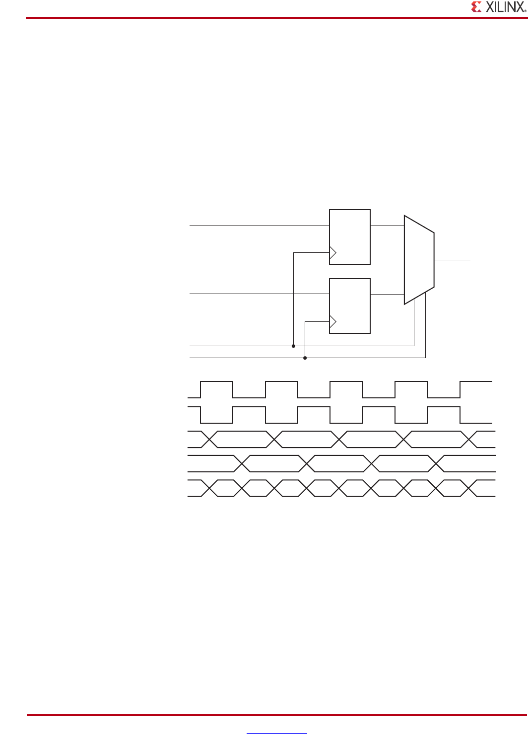
62 www.xilinx.com Spartan-6 FPGA SelectIO Resources
UG381 (v1.7) October 21, 2015
Chapter 2: SelectIO Logic Resources
The ODDR2 primitive supports the following modes of operation:
•NONE
•C0
•C1
The following sections describe each of the modes in detail.
NONE
The NONE mode uses the rising edges from both clocks C0 and C1. In this case, rising to
capture data D0 and D1, respectively. These two data bits are multiplexed by the DDR
multiplexer and forwarded to the output pin. Figure 2-11 shows this function.
C0 - Accept Input Alignment to Clock C0
The C0 mode outputs both data bits from the ODDR2 primitive on the rising edge of clock
C0. This mode is implemented using the DDR_ALIGNMENT attribute. Figure 2-12 shows
this function.
X-Ref Target - Figure 2-11
Figure 2-11: ODDR2 with DDR_ALIGNMENT = NONE
C0
D0
D1
C1
DQ
Q
D
From
FPGA
Logic
C0
C1
Q
D0
d + 1d
d + 2 d + 4 d + 6 d + 8d + 10d
d + 2 d + 3d + 4 d + 5 d + 6 d + 7 d + 8
Q
D1 d + 3d + 5 d + 7 d + 9d + 1
UG381_c2_12_102510
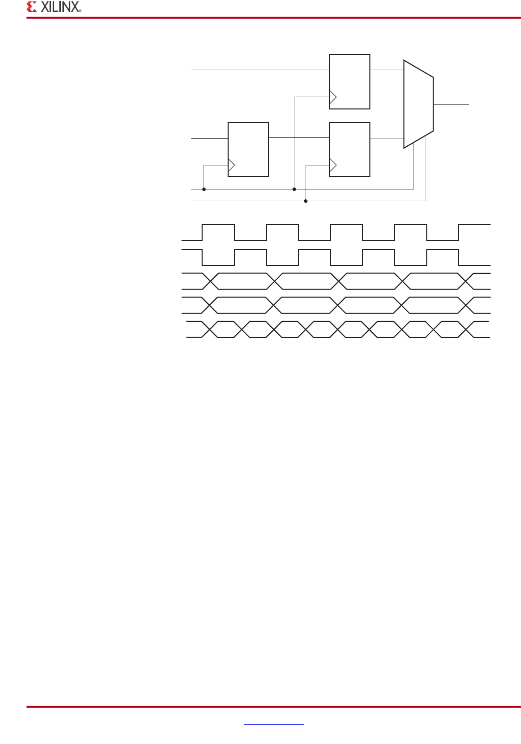
Spartan-6 FPGA SelectIO Resources www.xilinx.com 63
UG381 (v1.7) October 21, 2015
OLOGIC2 Resources
C1 - Accept Input Alignment to Clock C1
The C1 mode outputs both data bits from the ODDR2 primitive on the rising edge of clock
C1. This mode is implemented using the DDR_ALIGNMENT attribute. Figure 2-13 shows
this function.
X-Ref Target - Figure 2-12
Figure 2-12: ODDR2 with DDR_ALIGNMENT = C0
C0
D0
D1
C1
DQ
Q
D
From
FPGA
Logic
C0
C1
QDQ
UG381_c2_12_102510
Q
D0
d + 1d
d + 2 d + 4 d + 6 d + 8d
d + 2 d + 3d + 4 d + 5 d + 6 d + 7
D1 d + 3d + 5 d + 7 d + 9d + 1
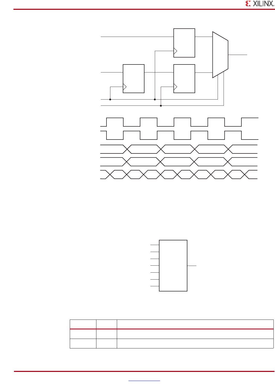
64 www.xilinx.com Spartan-6 FPGA SelectIO Resources
UG381 (v1.7) October 21, 2015
Chapter 2: SelectIO Logic Resources
ODDR2 Primitive
Figure 2-14 shows the ODDR2 primitive. Table 2-5 lists the ODDR2 port signals. Table 2-6
describes the various attributes available and default values for the ODDR2 primitive.
X-Ref Target - Figure 2-13
Figure 2-13: ODDR2 with DDR_ALIGNMENT = C1
C1
D0
D1
C0
DQ
Q
D
From
FPGA
Logic
C0
C1
QDQ
UG381_c2_13_111910
Q
D0
d + 1d
d + 2 d + 4 d + 6 d + 8d
d + 2 d + 3d + 4 d + 5 d + 6 d + 7
D1 d + 3d + 5 d + 7 d + 9d + 1
X-Ref Target - Figure 2-14
Figure 2-14: ODDR2 Primitive
Table 2-5: ODDR2 Port Signals
Port Name Type Description
D0 Input Input data from FPGA logic
D1 Input Input data from FPGA logic
UG381_c2_13_031909
D0
C1 Q
ODDR2
C0
D1
CE
R
S
Spartan-6 FPGA SelectIO Resources www.xilinx.com 65
UG381 (v1.7) October 21, 2015
OLOGIC2 Resources
ODDR2 VHDL and Verilog Templates
The Libraries Guide includes templates for instantiation of the ODDR2 primitive in VHDL
and Verilog.
OLOGIC2 Timing Models
This section describes the timing associated with various resources within the OLOGIC2
block. Table 2-7 summarizes the OLOGIC2 switching characteristics defined in the
Spartan-6 FPGA Data Sheet.
C0 Input Clock input, optionally invertible
C1 Input Second clock input inverted 180° relative to C0, optionally invertible
CE Input Clock enable
R Input Reset. Software will issue an error if both R and S are connected to 1
S Input Set. Software will issue an error if both R and S are connected to 1
Q Output Data output
Table 2-6: ODDR2 Attribute Summary
Attribute Name Possible
Values Default Value Description
DDR_ALIGNMENT NONE, C0,
and C1 NONE
Set DDR output alignment mode.
When used bidirectionally, the
mode must agree with the
corresponding IDDR2 mode.
INIT 0 or 1 0 Initialization value on output Q
SRTYPE ASYNC or
SYNC SYNC Set/Reset type
Table 2-5: ODDR2 Port Signals (Cont’d)
Port Name Type Description
Table 2-7: OLOGIC2 Switching Characteristics
Symbol Description
Setup/Hold
TODCK/TOCKD D1/D2 pins Setup/Hold with respect to CLK
TOOCECK/TOCKOCE CE pin Setup/Hold with respect to CLK
TOSRCK/TOCKSR SR pin Setup/Hold with respect to CLK
TOTCK/TOCKT T1/T2 pins Setup/Hold with respect to CLK
TOTCECK/TOCKTCE CE pin Setup/Hold with respect to CLK
Clock to Out
TOCKQ C0 to Q out
TRQ SR pin to Q out
66 www.xilinx.com Spartan-6 FPGA SelectIO Resources
UG381 (v1.7) October 21, 2015
Chapter 2: SelectIO Logic Resources
Timing Characteristics
Figure 2-15 illustrates the OLOGIC2 output register timing.
Clock Event 1
At time TOOCECK before Clock Event 1, the output clock enable signal becomes valid-high
at the CE input of the output register, enabling the output register for incoming data.
At time TODCK before Clock Event 1, the output signal becomes valid-high at the D input
of the output register and is reflected at the Q output at time TOCKQ after Clock Event 1.
Clock Event 4
At time TOSRCK before Clock Event 4, the R signal (configured as synchronous reset in this
case) becomes valid-high, resetting the output register and reflected at the Q output at time
TRQ after Clock Event 4.
Figure 2-16 illustrates the OLOGIC2 ODDR register timing using
DDR_ALIGNMENT = NONE mode.
X-Ref Target - Figure 2-15
Figure 2-15: OLOGIC2 Output Register Timing Characteristics
12345
C
D
CE
SR
Q
TOCKQ
TODCK
TOOCECK
TOSRCK
TRQ
ug381_c2_14_120810
Spartan-6 FPGA SelectIO Resources www.xilinx.com 67
UG381 (v1.7) October 21, 2015
OLOGIC2 Resources
Clock Event 1
At time TOOCECK before Clock Event 1, the ODDR clock enable signal becomes valid-High
at the CE input of the ODDR, enabling ODDR for incoming data. Care must be taken to
toggle the CE signal of the ODDR register between the rising edges and falling edges of C0
as well as meeting the register setup-time relative to both clock edges. Typically, in high-
speed applications, the CE signal is tied High.
At time TODCK before Clock Event 1 (rising edge of C0), the data signal D0 becomes valid-
high at the D0 input of ODDR register and is reflected on the Q output at time TOCKQ after
Clock Event 1.
Clock Event 2
At time TODCK before Clock Event 2 (rising edge of C1), the data signal D1 becomes valid-
high at the D1 input of ODDR register and is reflected on the Q output at time TOCKQ after
Clock Event 2 (no change at the Q output in this case).
Clock Event 9
At time TOSRCK before Clock Event 9 (rising edge of C0), the SR signal (configured as
synchronous reset in this case) becomes valid-high resetting ODDR register, reflected at the
Q output at time TRQ after Clock Event 9 (no change at the Q output in this case) and
resetting ODDR register, reflected at the Q output at time TRQ after Clock Event 10 (no
change at the Q output in this case).
X-Ref Target - Figure 2-16
Figure 2-16: OLOGIC2 ODDR Register Timing Characteristics
1234567891011
TODCK
TOOCECK
TODCK
TOSRCK
TRQ
C1
C0
D0
D1
CE
SR
Q
TOCKQ
ug381_c2_15_042409
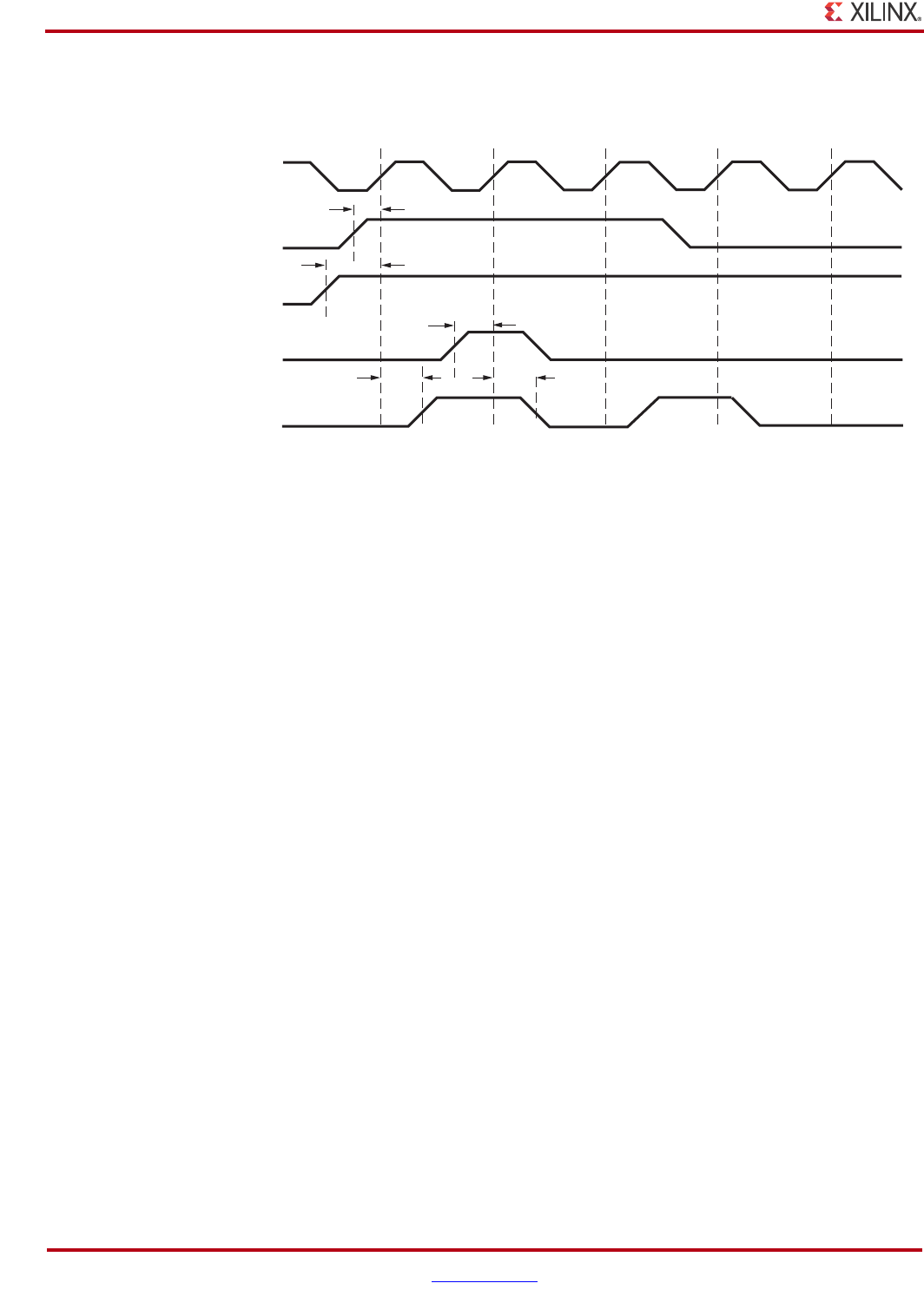
68 www.xilinx.com Spartan-6 FPGA SelectIO Resources
UG381 (v1.7) October 21, 2015
Chapter 2: SelectIO Logic Resources
Figure 2-17 illustrates the OLOGIC2 3-state register timing.
Clock Event 1
At time TOTCECK before Clock Event 1, the 3-state clock enable signal becomes valid-high
at the TCE input of the 3-state register, enabling the 3-state register for incoming data.
At time TOTCK before Clock Event 1 the 3-state signal becomes valid-high at the T input of
the 3-state register, returning the pad to high-impedance at time TOCKQ after Clock Event 1.
Clock Event 2
At time TOSRCK before Clock Event 2, the SR signal (configured as synchronous reset in this
case) becomes valid-high, resetting the 3-state register at time TRQ after Clock Event 2.
X-Ref Target - Figure 2-17
Figure 2-17: OLOGIC2 3-State Register Timing Characteristics
12345
CLK
T1
TCE
SR
TQ
TOCKQ TRQ
TOTCK
TOTCECK
TOSRCK
UG381_c2_16_051209
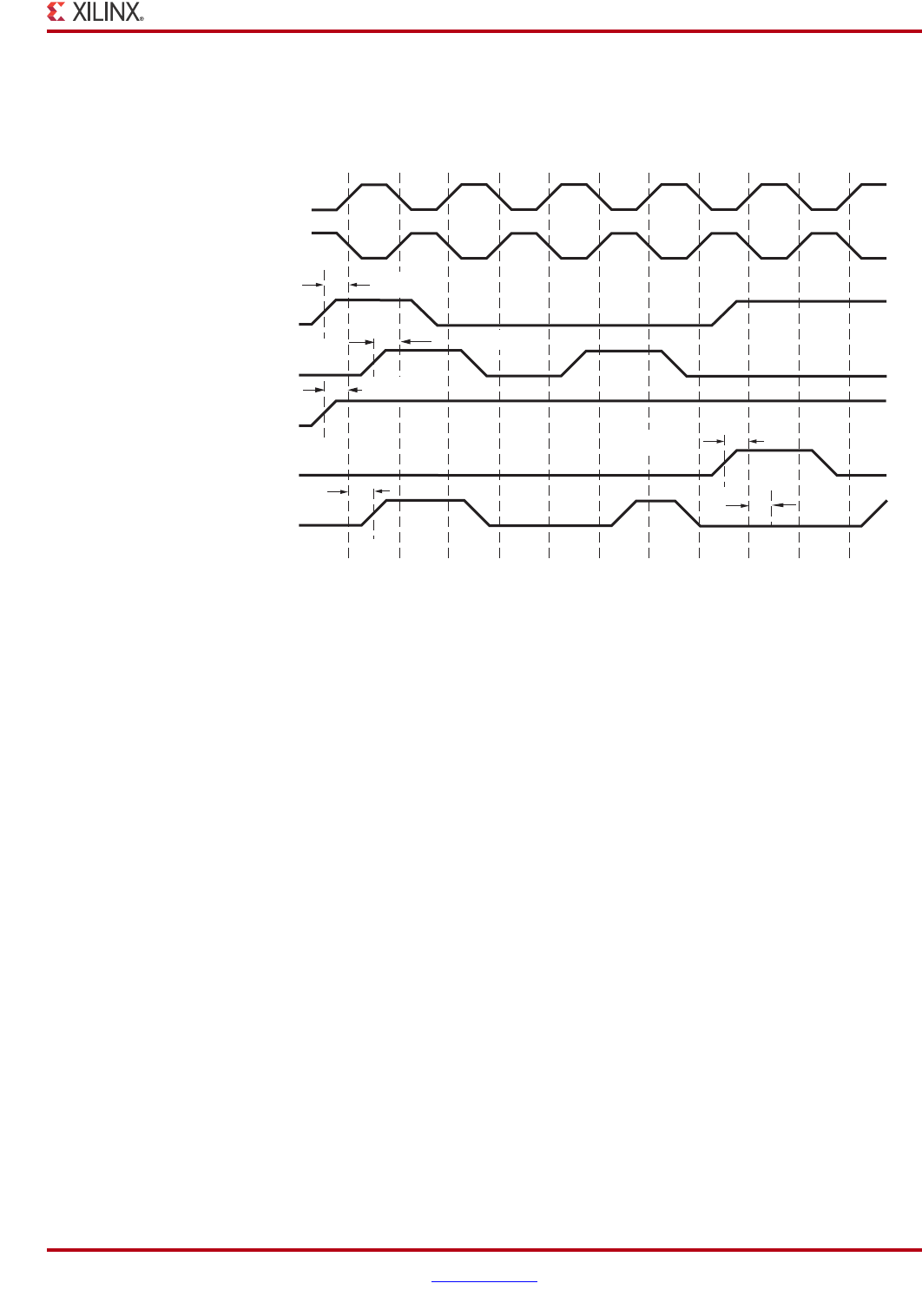
Spartan-6 FPGA SelectIO Resources www.xilinx.com 69
UG381 (v1.7) October 21, 2015
OLOGIC2 Resources
Figure 2-18 illustrates IOB DDR 3-state register timing. This example is shown using
DDR_ALIGNMENT = NONE.
Clock Event 1
At time TOTCECK before Clock Event 1, the 3-state clock enable signal becomes valid-High
at the CE input of the 3-state ODDR register, enabling them for incoming data. Care must
be taken to toggle the CE signal of the 3-state ODDR between the rising edges and falling
edges of C0 as well as meeting the register setup-time relative to both clock edges.
At time TOTCK before Clock Event 1 (rising edge of C0), the 3-state signal T0 becomes
valid-high at the T0 input of 3-state register and is reflected on the TQ output at time
TOCKQ after Clock Event 1.
Clock Event 2
At time TOTCK before Clock Event 2 (falling edge of C0), the 3-state signal T1 becomes
valid-high at the T1 input of 3-state register and is reflected on the TQ output at time
TOCKQ after Clock Event 2 (no change at the TQ output in this case).
Clock Event 9
At time TOSRCK before Clock Event 9 (rising edge of C0), the SR signal (configured as
synchronous reset in this case) becomes valid-high resetting 3-state Register, reflected at
the TQ output at time TRQ after Clock Event 9 (no change at the TQ output in this case) and
resetting 3-state Register, reflected at the TQ output at time TRQ after Clock Event 10 (no
change at the TQ output in this case).
X-Ref Target - Figure 2-18
Figure 2-18: OLOGIC2 ODDR 3-State Register Timing Characteristics
1234567891011
TOTCK
TOTCECK
TOTCK
TOSRCK
TRQ
C0
C1
T0
T1
CE
SR
TQ
TOCKQ
ug381_c2_17_120810
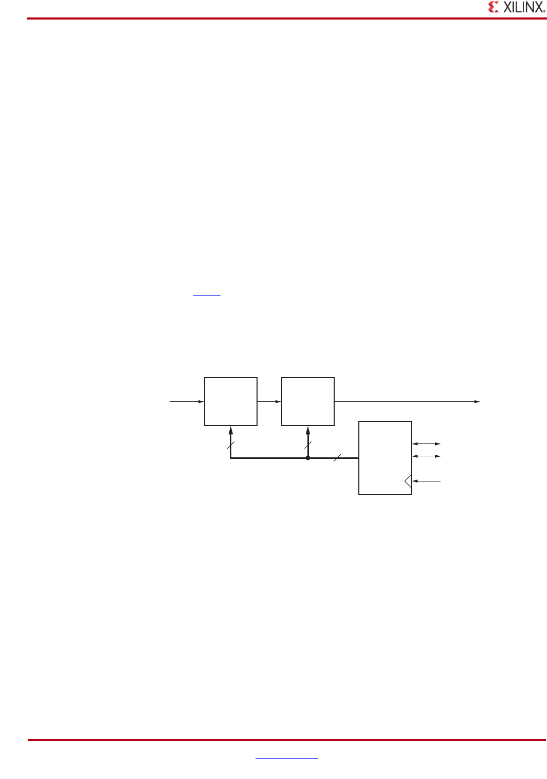
70 www.xilinx.com Spartan-6 FPGA SelectIO Resources
UG381 (v1.7) October 21, 2015
Chapter 2: SelectIO Logic Resources
I/O Delay Overview
Each IOB in the Spartan-6 FPGA contains a delay line that can be configured either for use
as an input delay or output delay. Different from the Virtex-5 FPGA structures, the
Spartan-6 FPGA delay is not compensated for either temperature or voltage, though there
are mechanisms that allow the user to accurately calibrate the delay on an on-going basis.
The delay block can be used as an input delay, an output delay, or when a bidirectional pin
is used, can switch between input and output delay under control of the T pin. In this case,
the input and output delays can be set to different values. The variable modes of the delay
line only apply when the delay is being used as an input. The variable modes of the delay
line do not apply when it is being used as an output. When using bidirectional delays, the
T pin of the primitive is used to select between the input and output delay mode.
Figure 2-19 shows the basic structure of the delay line. An 8-bit delay value allows delays
from 0 to 255 taps to be achieved. The three LSBs of this value control the starting point of
a ring oscillator. The oscillator is triggered by the arrival of an input signal, and its output
clocks a 5-bit counter from 0 to 7 tap delays later. The 5-bit counter is preset by the five
MSBs of the delay line value, and loops from 0 to 31 times before its output toggles to the
value originally input to the block. In this manner, delay resolution of one tap over the full
255 tap operating range is achieved. Maximum delays for each tap of the ring oscillator are
specified in DS162: Spartan-6 FPGA Data Sheet. Minimum delays are calculated during the
timing phase of the implementation tools and are available by generating the timing
reports. When using calibration-based modes (VARIABLE_FROM_ZERO,
VARIABLE_FROM_HALF_MAX, and DIFF_PHASE_DETECTOR) the minimum
operational frequency (FMINCAL) is determined by the minimum delay achievable through
a full delay block of 256 taps.
The delay line has two limitations. First, it should only be used to delay signals by a
maximum of one bit period, because bit errors can occur beyond this limit. Second,
processing of an edge must be complete before another edge arrives. This can occur when
receiving high speed data streams having noticeable jitter.
The first limitation is avoided by always keeping the delay less than the incoming bit
period (1 UI). Typically, the delay is set to 0.5 UI to enable data sampling to be centered in
the middle of the eye. The second limitation is avoided since each block actually contains
two delay lines as shown in Figure 2-20.
One delay line delays positive input transitions, and the other delay line delays negative
input transitions. When adjusting delay values, both blocks change together to ensure
positive and negative changes are delayed equally.
X-Ref Target - Figure 2-19
Figure 2-19: Delay Line Building Block
UG381_c2_08_051209
Data
Input
Delayed
Data Input
To/From FPGA Fabric
Global Clock
Ring
Oscillator
5-bit
Counter
35
8
User
Interface
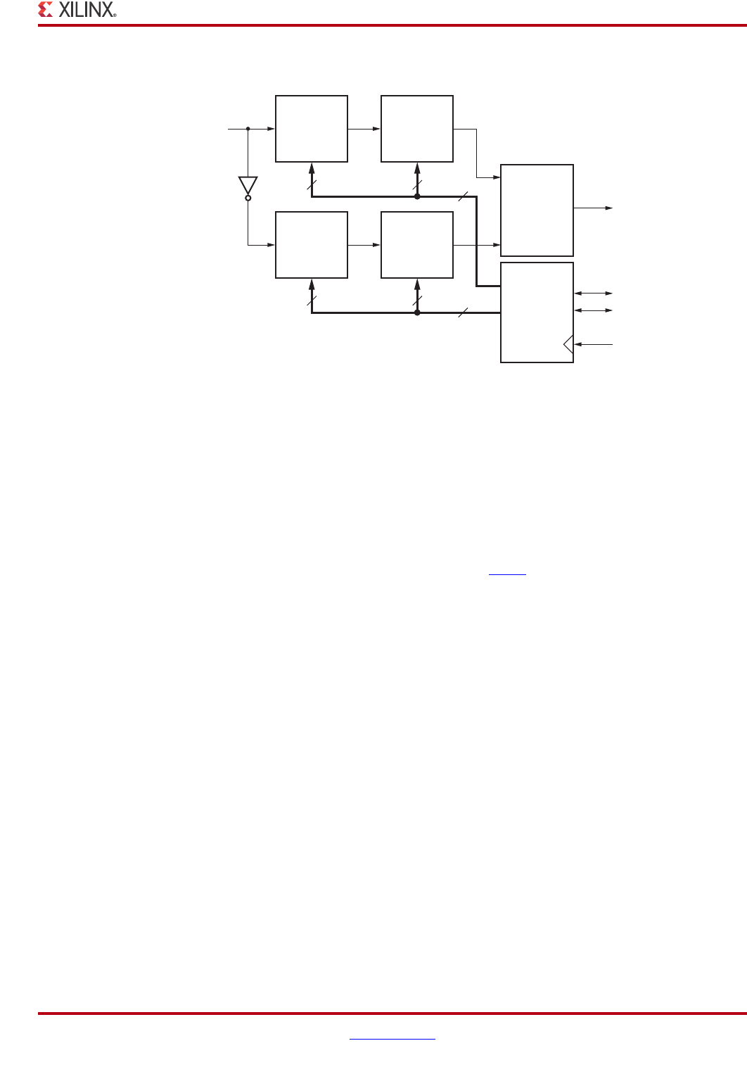
Spartan-6 FPGA SelectIO Resources www.xilinx.com 71
UG381 (v1.7) October 21, 2015
I/O Delay Overview
I/O Delay Modes
The input or output delay can act in one of several distinct modes:
• When used as an output delay, only the FIXED mode is available and the primitive
takes a value of a fixed number of delay steps that is set during design entry to be a
constant from 0 to 255. For the output delay (output only) use cases,
ODELAY_VALUE should be limited to less than 3/4 of the bit period determined
from the maximum tap timings specified in DS162: Spartan-6 FPGA Data Sheet.
• When used as an input delay, various modes are possible, and are selected via the
IDELAY_TYPE attribute.
• The DEFAULT mode sets the input delay to tap 0. This mode does not require any
input clocks to be applied.
• The DIFF_PHASE_DETECTOR mode is used for differential data signals. It is only
available when the delay line is used for input signals. See IDELAY_TYPE in
Table 2-9. Differential phase detector mode always uses both a master and a slave
IODELAY2. The slave unit has complete control of the master unit to avoid any data
loss occurring during changes to the input delay value. In this mode, the BUSY signal
is asserted after (re)programming, and stays asserted until four data transitions have
passed through the delay element.
• The FIXED mode sets the input delay to a fixed number of delay taps set by design
entry to be a constant from 0 to 255. This mode does not require any input clocks to be
applied. This mode is available for delaying either input or output or bidirectional
signals. A separate FIXED value is available for each direction of the delay line
(IDELAY_VALUE and ODELAY_VALUE). If a zero or negative hold time is needed,
timing analysis should be used to determine an appropriate FIXED tap value.
• The VARIABLE_FROM_ZERO and VARIABLE_FROM_HALF_MAX modes describe
the behavior of the input delay following execution of the calibrate and reset
commands. VARIABLE_FROM_ZERO sets the delay to 0 following calibration which
can be incremented and, once incremented, can also be decremented by amounts of
X-Ref Target - Figure 2-20
Figure 2-20: Using Two Delay Lines Per Delay Block
UG381_c2_09_051209
Data
Input
To/From
FPGA Logic
Global Clock
Ring
Oscillator
5-bit
Counter
35
8
User
Interface
Delayed Data Input
S-R
Logic
Ring
Oscillator
5-bit
Counter
Positive Transition Delay Line
Negative Transition Delay Line
35
8

72 www.xilinx.com Spartan-6 FPGA SelectIO Resources
UG381 (v1.7) October 21, 2015
Chapter 2: SelectIO Logic Resources
one delay tap. VARIABLE_FROM_HALF_MAX sets the delay value to half the
calculated maximum number of steps corresponding to one input clock period, and
can then be incremented and decremented from that value. This mechanism is
described in I/O Delay Calibration and Reset. These modes are only available when
the delay line is being used for delaying input signals. In these modes, the BUSY
signal is asserted after (re)programming, and stays asserted until four data transitions
have passed through the delay element.
• The COUNTER_WRAPAROUND attribute defines behavior of the delay primitive
when it increments to maximum value defined as the number of delay taps
corresponding to the input bit period. Setting the COUNTER_WRAPAROUND
attribute to WRAPAROUND forces the delay to wrap around to 0 when incremented.
Setting it to STAY_AT_LIMIT forces the delay to ignore the increment command
remain at maximum value. Use of COUNTER_WRAPAROUND prevents bit errors
from occurring due to the input delay being longer than one UI (the bit period).
• When used as a bidirectional delay, the ODELAY value should be set to 0. The modes
that are specified for input delay only are also available in bidirectional mode.
I/O Delay Calibration and Reset
A calibration mechanism is built into each IOB to compensate for the effects of
temperature, voltage and process on the individual delays in the IODELAY2 block. This
mechanism allows calibration of the IODELAY2 block against a known signal. In this
mechanism the I/O clock applied to the IODELAY2 block is used as the known signal.
Calibration is a process using the CAL and RST input pins on the IODELAY2 primitive.
When an active High CAL command is issued to the delay block, it enters a special mode
where the number of delay steps between rising edges on the I/O clock input are
calculated. Calibration takes between 12 and 20 global clock cycles depending on the ratio
between the global clock and the I/O clock. During this period, BUSY is asserted and the
data output from the block is invalid. The calculated value is stored in the delay block and
loaded only when an active High RST command is received. When an initial CAL
operation is performed and the RST command is received, the delay either becomes zero or
half the calculated value (half MAX) depending on the IDELAY_TYPE attribute defined at
design entry. Further CAL commands can then be issued at periodic intervals, but it is not
necessary to issue the RST command after the first calibration sequence. The calibration
sequence does not require transitions in the input data, but the RST sequence will not have
an effect on the delay line until four transitions are received on the input to the delay block.
Setting the delay line to half MAX delays the input data by exactly one half an input clock
cycle, allowing data sampling in the middle of the input data eye.
Once calibrated, the delay elements still vary with temperature and voltage.
Calibration Example
In this example, the delay taps have an average value of 40 ps under current operating
conditions. An I/O clock of 250 MHz (4,000 ps period) is applied to the IODELAY2 via
CLK0 for SDR mode. When the calibrate (CAL) command is issued, a value of
4,000/40 = 100 is returned internally. If the input delay is programmed to be
VARIABLE_FROM_HALF_MAX, then, following a reset (RST) command, the input delay
value is set to 50 taps, equivalent to approximately ½ the input clock period. As operating
conditions change, the average value of the delay taps will also change, as will the result
obtained from a CAL command. The reference design in XAPP1064, Source-Synchronous
Serialization and Deserialization (up to 1050 Mb/s) issues a CAL command every 210 global
clock cycles to ensure the values used by the delay block are adjusted adequately.
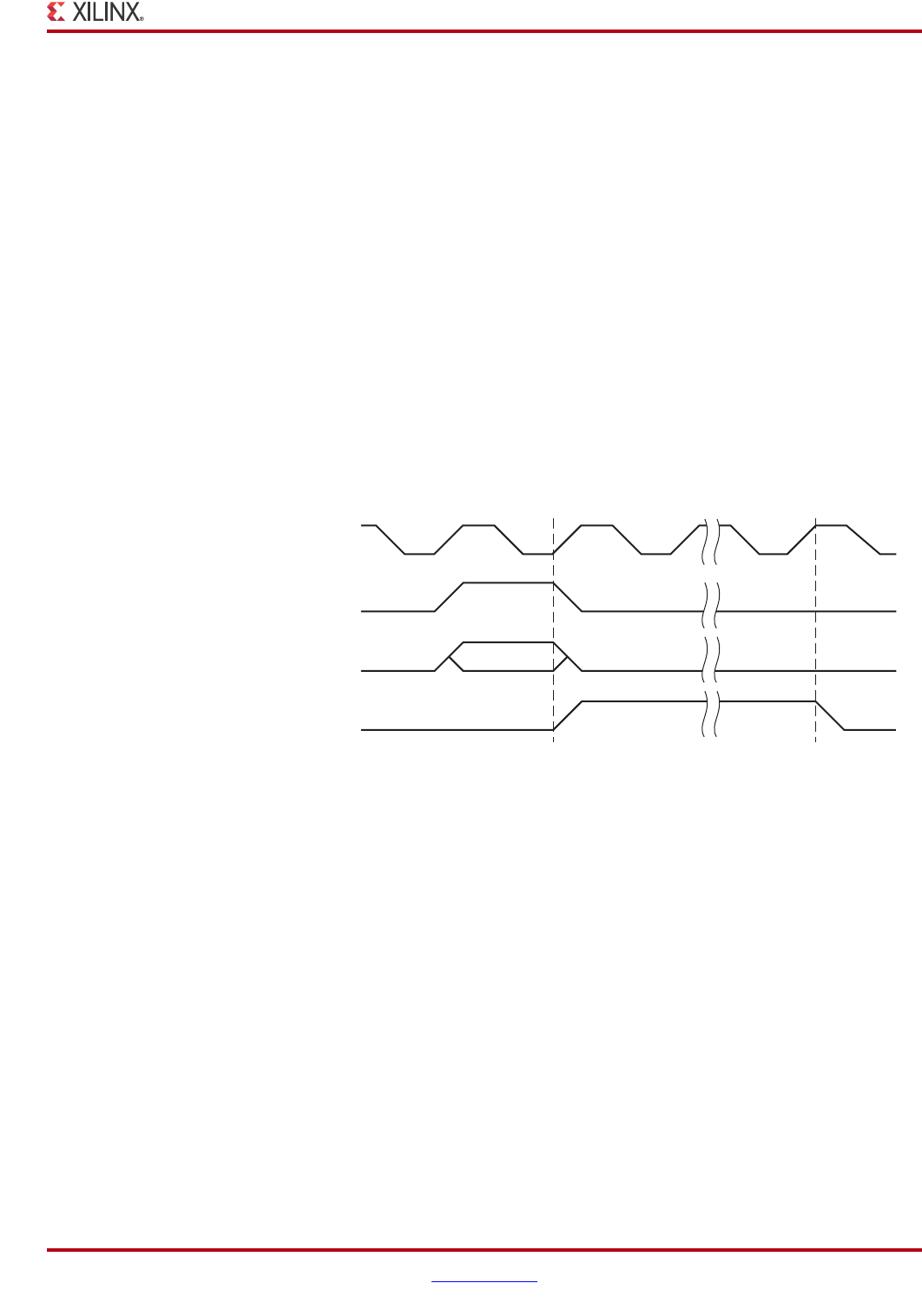
Spartan-6 FPGA SelectIO Resources www.xilinx.com 73
UG381 (v1.7) October 21, 2015
I/O Delay Overview
Calibration does not require a specific data input pattern, it only uses the high speed I/O
clock as a calibration source. However, any update in delay values only takes place after
four transitions in the input data stream occur. When in DDR mode, the IODELAY2
element requires two input clocks, 180° apart, which are doubled together inside the
element. This example, with incoming data of 250 Mb/s, implies that the required clocks
are 125 MHz and 125 MHz phase-shifted by 180°. When these input clocks are doubled
together, the clock internal to the IODELAY2 element runs at 250 MHz, and the operation
is identical to SDR mode. The two clocks are the same as used by an ISERDES2 (in DDR
mode) or IDDR2 element (if used) that follows the IODELAY2.
Delay Update and BUSY Timing
When the delay line is updated with a new value, as shown in Figure 2-21, this new value
is not immediately operational. Valid data reception during the update process is
necessary making synchronization extremely important. Once the design updates the
delay values, the BUSY signal transitions High to indicate that synchronization is in
progress. BUSY will not return Low until four input data transitions are received. Once
BUSY is Low, the new value is operational. In the absence of data transitions, BUSY can
stay asserted for long periods of time.
The timing of the BUSY pin is not always completely synchronous to DIVCLK. The BUSY
pin output is an OR of the internal busy signal, and a CLKDIV-registered version of this
signal. Under some conditions when performing a RST, INC, or DEC command, the
internal BUSY signal can assert and deassert within the word period framed by CLKDIV.
This is very dependent on the data pattern being received. If the necessary two transitions
for delay update occur close together, then a synchronous sampling flip-flop in the FPGA
interconnect logic might not appear to have changed the state of the BUSY signal since it is
sampled Low by two consecutive clock edges, even though it transitioned briefly High
between those two edges, and the delay is correctly updated. The internal logic driving the
BUSY pin is shown in Figure 2-22.
X-Ref Target - Figure 2-21
Figure 2-21: Delay Increment or Decrement Adjustment Timing
BUSY
INCDEC
CE
Global Clock
UG381_c2_10_021210
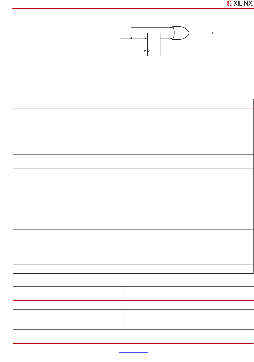
74 www.xilinx.com Spartan-6 FPGA SelectIO Resources
UG381 (v1.7) October 21, 2015
Chapter 2: SelectIO Logic Resources
IODELAY2 Primitive
X-Ref Target - Figure 2-22
Figure 2-22: BUSY Pin Signal Generation
UG381_c2_22_102110
Busy Pin
DIVCLK
Internal Busy Signal
Table 2-8: IODELAY2 Port List and Definitions
Port Name Type Description
IDATAIN Input Data Signal from the IOB.
T Input 3-state input signal from OLOGIC2 or OSERDES2. Forces the IODELAY2 to be an output
delay when Low, and an input delay when High.
ODATAIN Input Data input signal from OLOGIC2 or OSERDES2.
CAL Input Invokes the IODELAY2 calibration sequence. The calibration sequence lasts between eight
and 16 GCLK cycles. Drives BUSY Low when complete.
IOCLK0 Input Input from the I/O clock network. This is the primary clock input when the clock doubler
circuit is not engaged (see DATA_RATE attribute). Can be inverted.
IOCLK1 Input I/O clock network input. This is the secondary clock input and is only used when the clock
doubler is engaged (see DATA_RATE attribute). Can be inverted.
CLK Input Global clock network input. This is the clock for the FPGA logic interconnect domain.
INC Input Increment/decrement signal. Used for adjusting the tap setting up or down by one
increment or decrement. INC should only be asserted High when CE is also asserted High.
CE Input Clock enable for the increment/decrement signal.
RST Input Resets the IODELAY2 to either zero or half of an I/O clock period. The IDELAY_TYPE
attribute controls this choice.
BUSY Output Signals when calibration is complete or when synchronous tap delay update is complete.
DATAOUT Output Delayed data signal to D pin of ILOGIC2 or ISERDES2 sites.
DATAOUT2 Output Delayed data signal to FPGA interconnect logic.
TOUT Output Delayed 3-state signal to IOB when used as an output delay.
DOUT Output Delayed data signal to IOB when used as an output delay.
Table 2-9: IODELAY2 Attributes
Attribute Name Value Default
Value Description
IDELAY_VALUE Integer: 0–255 0 Defines the delay tap value for input delay mode.
IDELAY2_VALUE Integer: 0–255 0 Defines the delay tap value for secondary input
delay mode. Active only when IDELAY_MODE is
set to PCI.

Spartan-6 FPGA SelectIO Resources www.xilinx.com 75
UG381 (v1.7) October 21, 2015
I/O Delay Overview
IDELAY_MODE String: NORMAL or PCI NORMAL Chooses the delay mode setting. PCI is for
handling PCI applications. Affects input delays
only. Do not specify or modify this attribute.
ODELAY_VALUE Integer: 0–255 0 Defines the delay tap value for output delay
mode.
IDELAY_TYPE String: FIXED, DEFAULT,
VARIABLE_FROM_ZERO,
VARIABLE_FROM_HALF_MAX,
DIFF_PHASE_DETECTOR
DEFAULT Chooses the type of delay.
FIXED enables a fixed input delay, and requires no
clocks applied to the block.
DEFAULT sets the input delay to tap 0.
VARIABLE enables the increment/decrement
delay mode and permits calibration.
VARIABLE_FROM_ZERO and
VARIABLE_FROM_HALF_MAX enables the type
of reset behavior when the RST pin is asserted.
DIFF_PHASE_DETECTOR enables a mode where
the master and slave IODELAY2s and ISERDES2s
are cascaded for use with an optional phase
detector. In this mode, the master is set to half
MAX and the slave is set to zero when the RST pin
is asserted.
COUNTER_WRAP
AROUND
String: STAY_AT_LIMIT,
WRAPAROUND
STAY_AT_
LIMIT
Chooses the behavior when maximum or
minimum tap count is exceeded. Depends on
whether tap setting is being incremented or
decremented. Ensures that tap count always stays
in the correct operating range.
DELAY_SRC String: IO, ODATAIN,
IDATAIN
IDATAIN Indicates where the IODELAY2 input is coming
from.
ODATAIN indicates delay source is the
ODATAIN pin from the OSERDES2 or OLOGIC2.
IDATAIN indicates the delay source is from an
input pin.
IO indicates that the signal source switches
between IDATAIN and ODATAIN depending on
the sense of the T (3-state) input.
SERDES_MODE String: NONE, MASTER,
SLAVE
NONE When IODELAY2 is used in conjunction with
ISERDES2, the attribute defines whether
ISERDES2 stands alone or is a cascaded master or
slave.
SIM_TAP_DELAY Integer: 20–100 50 A simulation only attribute. Allows setting the
nominal tap delay to test different values for
simulation.
DATA_RATE SDR, DDR SDR Data rate settings. An SDR clock can be supplied
by a BUFIO2 clock, a BUFPLL clock, or a global
clock. A DDR clock can be supplied by two
separate BUFIO2 clocks or by one or two global
clocks.
Table 2-9: IODELAY2 Attributes (Cont’d)
Attribute Name Value Default
Value Description

Spartan-6 FPGA SelectIO Resources www.xilinx.com 77
UG381 (v1.7) October 21, 2015
Chapter 3
Advanced SelectIO Logic Resources
ISERDES2 Overview
Each IOB contains an input deserializer block that can be instantiated in a design by using
the ISERDES2 primitive. ISERDES2 allows serial-to-parallel conversion with SerDes ratios
of 1:2, 1:3, and 1:4. The SerDes ratio is the ratio between the high speed I/O clock that is
capturing data, and the slower internal global clock used for processing the parallel data.
For example, with a single-rate I/O clock running at 500 MHz to receive data at 500 Mb/s,
the ISERDES2 transfers four bits of data at one quarter of the rate (125 MHz) to the FPGA
logic.
When using differential inputs, the two ISERDES2 primitives associated with the two IOBs
can be cascaded to allow higher SerDes ratios of 1:5, 1:6, 1:7, and 1:8.
Each ISERDES2 also contains logic to word-align the parallel data, as required by the
designer, by performing a Bitslip operation.
ISERDES2 Ports and Attributes
Table 3-1 lists the available ports in the ISERDES2 primitive.
Table 3-1: ISERDES2 Port List and Definitions
Port Name Type Description
CLK0 Input I/O clock network input. Optionally inverted. This is the primary clock input used when
the clock doubler circuit is not engaged (see DATA_RATE attribute).
CLK1 Input I/O clock network input. Optionally inverted. This secondary clock input is only used
when the clock doubler is engaged (see DATA_RATE attribute).
CLKDIV Input Global clock network input. This is the clock for input data and control signals from the
FPGA logic domain.
CE0 Input Clock enable input for all registers.
BITSLIP Input Invoke Bitslip when High. Synchronous to CLKDIV. Bitslip operation can be used with
any DATA_WIDTH, cascaded or not.
D Input Input data. This is the data input after being delayed by the IODELAY2 block.
RST Input Asynchronous reset only.
IOCE Input
Data strobe signal derived from BUFIO2 or BUFPLL CE. Strobes data capture to be
correctly timed with respect to the I/O and global clocks for the SerDes mode selected.
Reregistered inside the ISERDES2.
78 www.xilinx.com Spartan-6 FPGA SelectIO Resources
UG381 (v1.7) October 21, 2015
Chapter 3: Advanced SelectIO Logic Resources
Table 3-2 summarizes all the applicable ISERDES2 attributes. For more information on
applying these attributes in UCF, VHDL, or Verilog code, refer to the Xilinx ISE Software
Manual.
SHIFTIN Input
Cascade-in signal for master/slave I/O. Used when master and slave sites are used
together for DATA_WIDTHs greater than four. When the block is a master, it transfers
data in for use in the phase-detector mode. When the block is a slave, it transfers serial
data in to become parallel data.
CFB0 Output Feed-through route to allow a PLL or DCM generated clock to feed back to the PLL or
DCM through a BUFIO2FB.
CFB1 Output Secondary feed-through route to allow a PLL or DCM generated clock to feed back to the
PLL or DCM through a BUFIO2FB.
DFB Output Feed-through route to allow an input clock that has been delayed in an IODELAY2
element to be forwarded to a DCM, PLL, or BUFG through a BUFIO2.
SHIFTOUT Output
Cascade-out signal for master/slave I/O. In slave mode, it is used to send sampled data
from the slave. In master mode, it sends serial data from the 4th stage of the input shift
register to the slave.
FABRICOUT Output Asynchronous data for use in the FPGA logic.
Q4, Q3, Q2, Q1 Outputs Registered outputs to FPGA logic.
VALID O u tput
Output of the phase detector in master mode (dummy in slave mode). If the input data
contains no edges (no information for the phase detector to work with) the VALID signal
transitions Low to indicate that the FPGA logic should ignore the INCDEC signal.
INCDEC Output Output of phase detector in master mode (dummy in slave mode). Indicates to the FPGA
logic whether the received data was sampled early or late.
Table 3-1: ISERDES2 Port List and Definitions (Cont’d)
Port Name Type Description
Table 3-2: ISERDES2 Block Attributes
Attribute Name Possible Values Default Value Description
DATA_RATE SDR, DDR SDR
Data rate settings. An SDR clock can be
supplied by a BUFIO2 clock, a BUFPLL clock,
or a global clock. A DDR clock can be supplied
by two separate BUFIO2 clocks or by one or
two global clocks.
DATA_WIDTH [2, 3, 4, 5, 6, 7, 8] 2
Data width. Defines the parallel data output
width of the serial-to-parallel converter. Values
greater than four are only valid when two
ISERDES2 blocks are cascaded. In this case, the
same value should be applied to both the
master and slave blocks.
BITSLIP_ENABLE TRUE, FALSE FALSE
Enables or disables the Bitslip function
controlled by the BITSLIP input pin. One bit is
slipped for every assertion of the BITSLIP
input pin, irrespective of the DATA_WIDTH
selected. When disabled, the Bitslip input pin is
inactive.
Spartan-6 FPGA SelectIO Resources www.xilinx.com 79
UG381 (v1.7) October 21, 2015
ISERDES2 Overview
ISERDES2 Operation
The logic contained in the ISERDES2 is shown in Figure 3-1. Serial data is received from the
pin (usually through an IODELAY2 block) and is clocked into a 4-bit shift register (A) by
the associated I/O clock. This I/O clock is running at the same speed as the incoming data
either through a PLL or the local clock doubling mechanism. No Double Data Rate (DDR)
techniques are required.
The four bits of parallel data are then transferred, using the I/O clock and the Bitslip clock
enable signal, into a parallel register (B). The outputs of B are then either made available to
the FPGA logic if the ISERDES2 is in NETWORKING mode, or further transferred using
the I/O clock and the incoming SerDes strobe signal IOCE into register set C. The outputs
of register set C are either made available to the FPGA logic if the ISERDES2 is in
NETWORKING_PIPELINED mode, or a further transfer occurs into the user global clock
domain, register set D. The outputs of register set D are available to the FPGA logic if the
ISERDES2 is in RETIMED mode.
The timing of the SerDes strobe ensures correct and loss-free transfer of data as shown in
Figure 3-2 and Figure 3-3. The timing diagram for operation, shown in Figure 3-2 and
Figure 3-3, assumes a 1:4 deserialization is being performed. The timing of the SerDes
strobe is obviously critical to achieving correct functionality. This signal is generated either
by a BUFIO2 or by a BUFPLL, as described further in Spartan-6 FPGA Clocking Resources
User Guide. Figure 3-2 shows SDR operation, and Figure 3-3 shows DDR operation. These
are essentially identical except that the doubler is used to combine two input clocks (from
two different BUFIO2s) in DDR mode.
The output pins that are valid for the various SerDes ratios available are shown in
Table 3-3.
SERDES_MODE NONE, MASTER, SLAVE NONE
Indicates if the ISERDES2 is being used alone,
or as a master or slave, when two ISERDES2
blocks are cascaded.
INTERFACE_TYPE
NETWORKING,
NETWORKING_PIPELINED,
RETIMED
NETWORKING
Selects mode of operation and determines
which set of parallel data is available to the
FPGA logic.
Table 3-2: ISERDES2 Block Attributes (Cont’d)
Attribute Name Possible Values Default Value Description
Table 3-3: Data Connections When Using a Single ISERDES2 Primitive
Input SerDes Factor Pins to Use for Input to the FPGA Logic (MSB–LSB)
2Q4, Q3
3 Q4, Q3, Q2
4 Q4, Q3, Q2, Q1
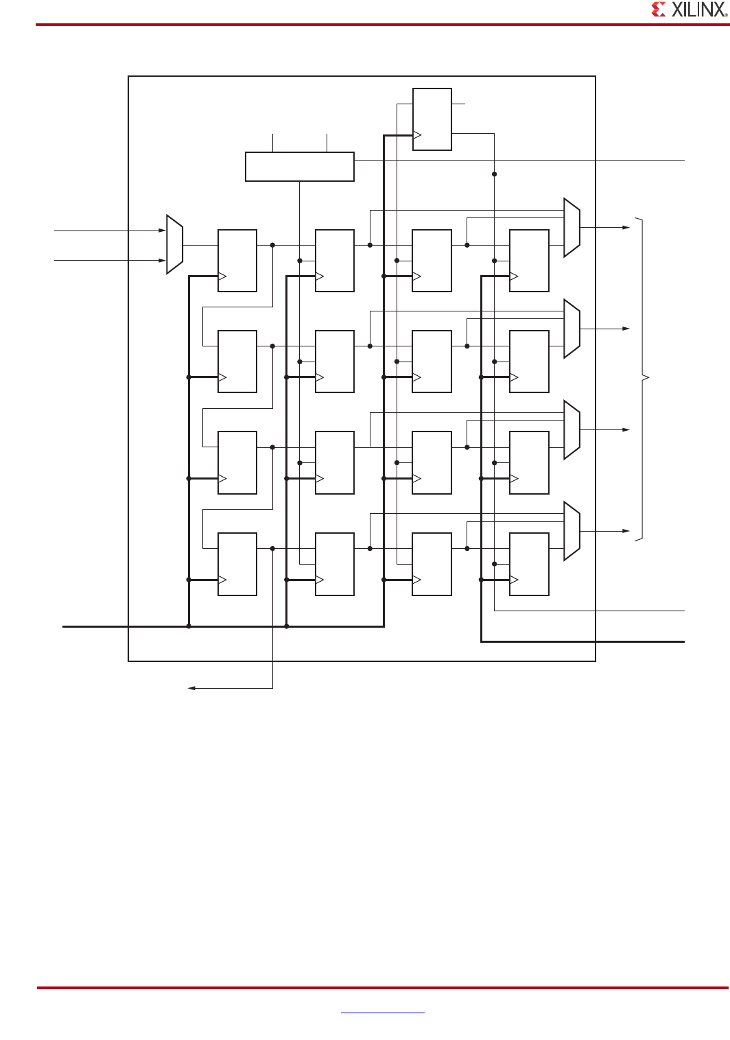
80 www.xilinx.com Spartan-6 FPGA SelectIO Resources
UG381 (v1.7) October 21, 2015
Chapter 3: Advanced SelectIO Logic Resources
X-Ref Target - Figure 3-1
Figure 3-1: Overview of the ISERDES2 Block in SDR Mode
UG381_c3_01_012413
D
Bitslip Logic
IOCLK CLK0
Outputs to FPGA logic from B are used in NETWORKING mode
Outputs to FPGA logic from C are used in NETWORKING + PIPELINED mode
Outputs to FPGA logic from D are used in RETIMED mode
Input data
from pin via
input delay
Q4
Q3
Q2
Q1
CE0
CLKDIV
Cascade In
I/O Clock Enable (IOCE)
(SerDes Strobe)
Bitslip enable
from FPGA logic
Internal Bitslip
clock enable
Parallel
data inputs
to FPGA
logic
Clock enable
from FPGA logic
Global clock
Cascade Out
AB
CD
D
CE
D
CE
D
CE
QD
CE
DD
CE
D
CE
D
CE
DD
CE
D
CE
D
CE
DD
CE
D
CE
D
CE
CLKDIV RST
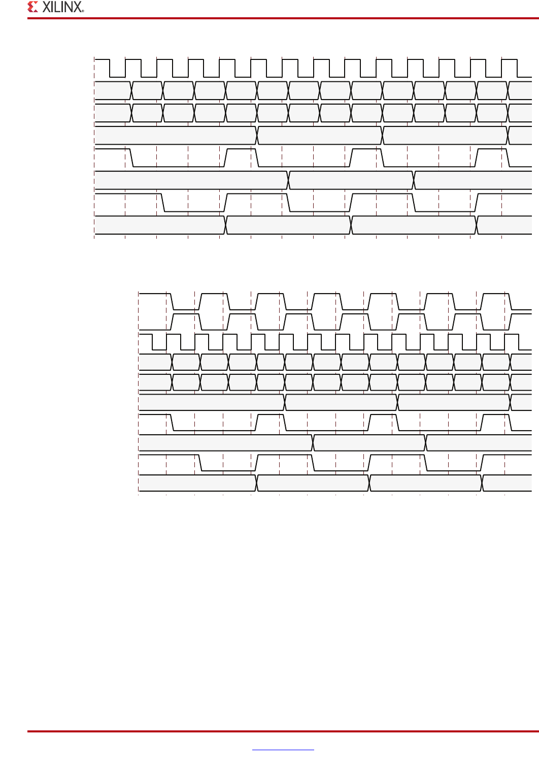
Spartan-6 FPGA SelectIO Resources www.xilinx.com 81
UG381 (v1.7) October 21, 2015
ISERDES2 Overview
NETWORKING Mode
When ISERDES2 is being used in NETWORKING mode, the BITSLIP function is not
supported.
NETWORKING_PIPELINED Mode
In this mode, the outputs of the IOCE enabled register bank (C) are made available to the
FPGA logic. The Bitslip operation can safely be used in this mode. The output data changes
a minimum (n – 1.5) I/O clocks before the rising edge of the global clock (generated via the
same BUFIO2 or PLL/BUFPLL that is generating the I/O clock), and if this timing is
acceptable, there are obvious data latency advantages over the RETIMED mode.
X-Ref Target - Figure 3-2
Figure 3-2: ISERDES2 Timing Diagram (SDR Operation)
I/O Clock = CLK0
Input Serial Data
Parallel Register A
Parallel Register B
SerdesStrobe IOCE
Parallel Register C
Global Clock
Parallel Register D
ABCDEFGHIJKLMN
Axxx BAxx CBAx DCBA EDCB FEDC GFED HGFE IHGF JIHG KJIH LKJI MLKJ
DCBA HGFE LKJI
DCBA HGFE
DCBA HGFE
UG381_c3_02_112013
X-Ref Target - Figure 3-3
Figure 3-3: ISERDES2 Timing Diagram (DDR Operation)
CLK0
CLK1
I/O Clock = CLK0 doubled with CLK1
Input Serial Data
Parallel Register A
Parallel Register B
SerdesStrobe IOCE
Parallel Register C
Global Clock
Parallel Register D
ABCDEFGHIJKLMN
Axxx BAxx CBAx DCBA EDCB FEDC GFED HGFE IHGF JIHG KJIH LKJI MLKJ
DCBA HGFE LKJI
DCBA HGFE
DCBA HGFE
UG381_c3_03_112013
82 www.xilinx.com Spartan-6 FPGA SelectIO Resources
UG381 (v1.7) October 21, 2015
Chapter 3: Advanced SelectIO Logic Resources
RETIMED Mode
In this mode the outputs of the final register bank (D) are made available to the FPGA
logic. This register contains data that has already been retimed to the global clock input.
For example, timing only becomes an issue when a SerDes ratio is:
• 2:1 (=DDR), where the I/O speed is limited to 500 Mb/s
• 3:1, where the I/O speed is limited to 750 Mb/s
All other SerDes ratios support the full data rate as specified in the data sheet. No issues
arise when using Bitslip in this mode. The global clock network pin (CLKDIV) is specified
in the data sheet to be fast enough to work under worst case SerDes conditions.
Cascade Operation
When using single-ended or differential data reception, the master ISERDES2 (associated
with the positive input pin) can be cascaded into the slave ISERDES2 (associated with the
negative input pin). This is achieved by connecting the SHIFTOUT port of the master
ISERDES2 to the SHIFTIN port of the slave ISERDES. These cascade connections are
shown in Figure 3-1.
The received data now has access to four banks of flip-flops as before, but in the cascaded
case, each bank is comprised of eight flip-flops. The SerDes strobe is modified accordingly
using the attribute on the BUFPLL or BUFIO2 which must match the attributes on the two
cascaded ISERDES2. In the case of single-ended data reception, this cascade has the effect
of making the synchronous input logic for the neighboring pin unavailable. The pin can
still be used as an asynchronous input or output.
Table 3-4 shows the data connections when using two cascaded ISERDES2 primitives.
Bitslip Operation
A designer can adjust the word alignment of the received data using a Bitslip operation.
BITSLIP should be asserted High for one CLKDIV cycle, and then deasserted for a
minimum of one CLKDIV cycle. Typically, this involves either a received framing signal, or
can be related to the received clock rising edge as implemented in video applications.
Bitslip occurs by modifying the timing of the clock enable applied to the Bitslip register (B).
Initially this timing is set to be one clock in advance of the main I/O clock enable signal
received from a BUFPLL or BUFIO2 as described in the Spartan-6 FPGA Clocking Resources
User Guide.
Table 3-4: Data Connections When Cascading Two ISERDES2 Primitives
Input SerDes Factor Pins to Use for Input to the FPGA Logic (MSB–LSB)
5 Master (Q4, Q3, Q2, Q1) and Slave (Q4)
6 Master (Q4, Q3, Q2, Q1) and Slave (Q4, Q3)
7 Master (Q4, Q3, Q2, Q1) and Slave (Q4, Q3, Q2)
8 Master (Q4, Q3, Q2, Q1) and Slave (Q4, Q3, Q2, Q1)
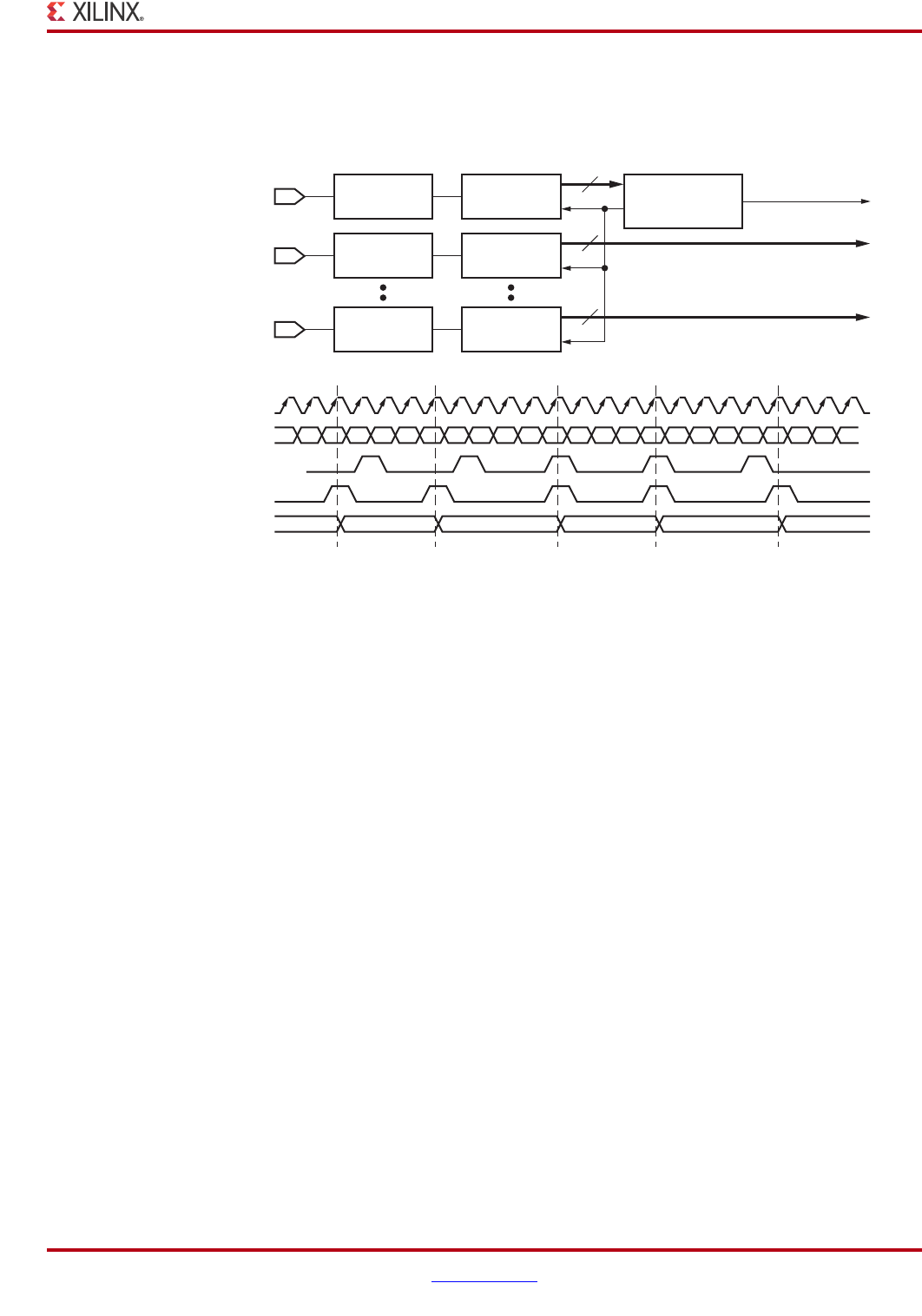
Spartan-6 FPGA SelectIO Resources www.xilinx.com 83
UG381 (v1.7) October 21, 2015
ISERDES2 Overview
An example, as shown in Figure 3-4, has n incoming data lines and one frame line that
contains the constant pattern 0001. Deserialization of 1:4 is required on all lines, with the
correct framing result when the received frame data pattern is equal to 0001.
The Bitslip state machine compares the incoming 4-bit data on the frame line with 0001,
and if the word is not properly framed, it issues a Bitslip command to all the ISERDES2
receiver lines. In the example shown, the received framing data is initially 0100. The
Bitslip state machine issues a Bitslip command, which effectively makes the received data
0010, and then issues another command to arrive at the required result of 0001. Once the
required bit pattern is detected, the designer has two possible results depending on the
system architecture. In theory, further Bitslip commands are not required and the state
machine can be disabled. However, if the Bitslip state machine is allowed to continue, then
any further detection of bad framing data indicates data corruption, and informs the
designer to take further action.
As all of the receiver ISERDESs are shifted in the same manner by the Bitslip commands,
the end result is that each 4-bit word of input data is correctly aligned to the framing
pattern.
When the Bitslip command is received, all of the ISERDESs internally perform a Bitslip
function. This is achieved by modifying the repetition period of the Bitslip clock enable
once (only) per command. In the example shown in Figure 3-4, the Bitslip clock enable line
is High for one in every four I/O clock cycles, thus capturing the last four serial data bits
received. When the Bitslip command is received, the Bitslip clock enable transitions High
for one in five I/O clock cycles, but once (only) per command. The last four serial bits
X-Ref Target - Figure 3-4
Figure 3-4: Bitslip Timing Diagram of ISERDES2 Block (4:1 illustrated)
Frame Input Serial Data
I/O Clock Enable
Bitslip Clock Enable
Parallel Register B
I/O Clock
4 clocks
between
Bitslip
clock
enables
Bitslip
command
issued
(synchronous
to global clock)
4 clocks
between
Bitslip
clock
enables
Bitslip
command
issued
(synchronous
to global clock)
5 clocks
between
Bitslip
clock enables
as a result of
bitslip command
5 clocks
between
Bitslip
clock enables
as a result of
Bitslip command
01 0010
0100 0100 0010 0010 0001
001000100010001000
4
4
4
Frame Input Data
Bitslip Complete
IODELAY2 ISERDES2Bitslip
State Machine
Input Data 0 IODELAY2 ISERDES2
Input Data n IODELAY2 ISERDES2
UG381_c3_04_111913

84 www.xilinx.com Spartan-6 FPGA SelectIO Resources
UG381 (v1.7) October 21, 2015
Chapter 3: Advanced SelectIO Logic Resources
received are still captured, but in addition, one received data bit is effectively discarded. In
the case of a serial line containing a constant data pattern, the effect is to rotate the received
data left by one bit. Bitslip can also be used when master and slave ISERDES2 are cascaded
for deserialization factors of 5:1, 6:1, 7:1, and 8:1. In this case, internal logic guarantees
synchronization between the master and slave ISERDES.
For clarity, the last bit received before the Bitslip clock enable is captured as the most
significant bit of the parallel word.
A synchronous reset to the ISERDES2 will force the Bitslip circuitry back to its initial
condition. A reset should always be issued in systems with multiple ISERDES2 using
Bitslip to ensure that all units are initially in the same state. An example of a typical
pseudo-code for the Bitslip state machine is shown:
After reset
If input frame data not equal to required frame pattern then
BITSLIP <= ‘1’
Else
BITSLIP <= ‘0’
BITSLIP_COMPLETE <= ‘1’
Wait at least one global clock cycle
Repeat
Phase Detector Overview
The phase detector works only in IODELAY2 differential input mode. It can be used with
single-ended signal inputs (_P pins only), but as the phase-detector mode requires two
IODELAY2 and two ISERDES2 primitives, the pin adjacent to the signal input can no
longer be used for synchronous inputs. The phase detector uses the flip-flops from the
master and slave ILOGIC blocks. There are two outputs synchronized to GCLK:
• INCDEC indicates the requirement to increment/decrement the delay line value
• VALID, when one or more valid edges detected
The phase detector operation uses both rising and falling transitions in the data. If there are
no transitions present, then the phase detector will not produce any adjustment signals.
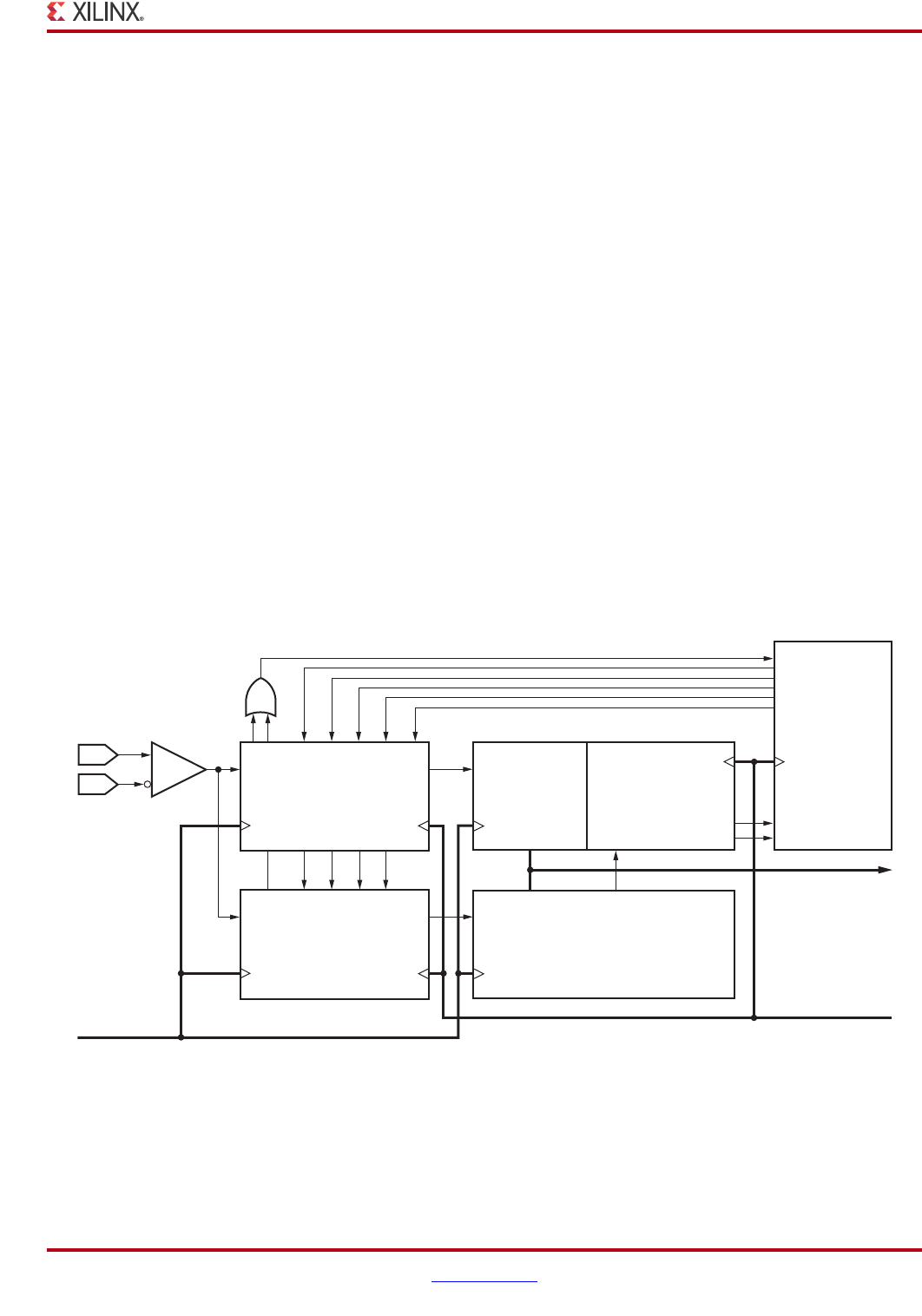
Spartan-6 FPGA SelectIO Resources www.xilinx.com 85
UG381 (v1.7) October 21, 2015
Phase Detector Overview
The phase detector uses inputs taken from the input sampling flip-flop:
•S3: master flip-flop output
•S2: master flip-flop output shifted by one IOCLK cycle
•E3: slave flip-flop output
An event occurs when an edge is detected on signal S3. The event controls the update of
the averaging counter. The counter stores samples for up to eight IOCLK cycles
When E3 is to left of the eye, the delay line needs to be incremented. When E3 is to right of
the eye, the delay line needs to be decremented. The phase detector compares E3 with S3
and increments or decrements the counter based on the previous comparison.
The phase detector can only be used with incoming differential data. This mechanism uses
a special mode for both the master and slave input delay elements
(IDELAY_TYPE = DIFF_PHASE_DETECTOR) and master and slave ISERDES2 logic.
The master SerDes has some extra built-in logic to enable the phase detector function. This
allows the incoming phase of the received data bit to be referred to the sampling I/O clock,
and determine if the sample is occurring early, before the middle of the eye, or late, after
the middle of the eye. To achieve this, there is a cascade path from the slave SerDes to the
master SerDes that transfers the information that has been registered in the slave to the
phase detector. Once the phase detector outputs are valid, the delays in the master and
slave input delay block can then be adjusted appropriately.
The data for deserialization and input to the FPGA logic always comes from the master
input delay. The slave input delay is just there to allow the phase-detector logic to function.
The overall topology of the phase detector is shown in Figure 3-5.
The indications of operation to the designer are output each global clock cycle, assuming
changes in the state of the data line in that period, and take the form of two signals; VALID
and INCDEC. If VALID is asserted, then one or more transitions have occurred, and
INCDEC indicates the direction to move the IODELAYs in time to ensure that the data is
X-Ref Target - Figure 3-5
Figure 3-5: Differential Data-Phase Detector Topology Overview
MASTER
IODELAY2
P
N
ug381_c3_05_111913
BUSYCE INC CAL RST
VALID
INCDEC
MASTER
ISERDES2
PHASE
DETECTOR
SLAVE
ISERDES2
PHASE
Detector
State
Machine
In FPGA
Logic
SLAVE
IODELAY2
IOCLK
Differential
Data Input
Signal
Global CLK
Parallel Data
To FPGA Logic
BUSYCE INC CALRST

86 www.xilinx.com Spartan-6 FPGA SelectIO Resources
UG381 (v1.7) October 21, 2015
Chapter 3: Advanced SelectIO Logic Resources
sampled in the middle of the eye. If VALID is deasserted either no data transitions
occurred, or the transitions that did occur have cancelled each other out because an equal
number occurred early as occurred late.
Due to the nature of the sampling mechanism and the input delay elements, which are
discrete taps, it is virtually impossible for the sample points to occur exactly in the middle
of the eye, so the VALID and INCDEC signals can potentially occur even if no action is
really required, and it is up to the designer to determine how best to update the delay lines.
This could be by updating immediately, or by using some sort of averaging state machine.
For example, if only one transition occurs during the global clock period, this would (by
design) result in a VALID being asserted.
Phase Detector Calibration Mechanisms
The phase-detector mechanism relies on the calibration function of the input delay.
Calibration also has to be performed periodically to ensure that the phase-detector
operation is working correctly. This mechanism is further discussed in I/O Delay
Calibration and Reset in Chapter 2, and is also part of the same controller state machine. In
the case where the phase detector is being used, calibration is performed in two slightly
different ways.
Initially, the state machine issues a CAL command to both the MASTER and SLAVE
IODELAY2 elements; each then uses the input clock to calibrate themselves to a value, but
does not yet load that value into the delay lines. This value corresponds to the number of
delay taps inside an input clock period where the value calculated equals MAX. A RST
command is then issued to both the MASTER and SLAVE IODELAY2 elements, this causes
the master delay to become half MAX (making it suitable for directly sampling the
incoming data in the middle of its eye), and the SLAVE value becomes zero. In addition, a
pipeline register stage is added into the slave delay. In this mode, the SLAVE delay is
always the MASTER delay minus half MAX.
Periodically, the state machine needs to recalibrate the SLAVE delay to ensure that as the
delay line values drift with voltage and temperature, data corruption cannot occur. This is
achieved by issuing a CAL command to the SLAVE IODELAY2 only; the unit then
calibrates itself, but data reception can continue as the MASTER delay is not modified by
this operation. Once the calibration command is issued to the SLAVE IODELAY2 only, a
value corresponding to the MASTER input delay is loaded (which again is not changed by
this operation) minus half MAX as before. When operating conditions in the device
change, then the value of MAX could also change, but the SLAVE delay remains half of the
clock period less than the MASTER delay.
During this recalibration sequence, the master delay is always valid, but the slave delay
effectively generates random data, and the results from the phase detector are therefore
invalid until the BUSY pin indicates completion of the commands.
This combination of calibration and dynamically adjusting the master delay appropriately
using the phase detector mechanism ensures correct data reception at very high bit rates.
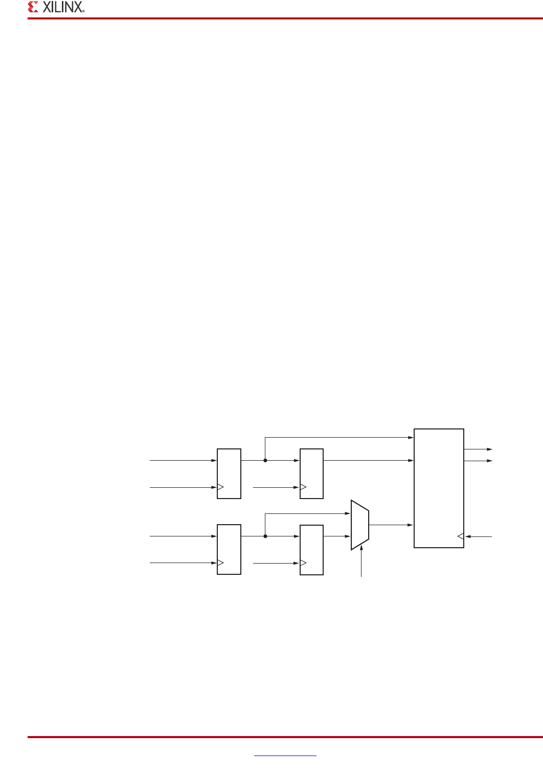
Spartan-6 FPGA SelectIO Resources www.xilinx.com 87
UG381 (v1.7) October 21, 2015
Phase Detector Overview
Phase Detector Operation
As discussed, in DIFF_PHASE_DETECTOR mode the master input delay is set up
following a calibration (CAL) command and a reset (RST) command to be half the
incoming I/O clock period that has been determined using the calibration mechanism of
the input delay. At the same time, the slave is set to be zero, that is the master input delay
minus half the incoming I/O clock period (half MAX). Once calibrated, any increments or
decrements to the master delay result in that calculated new value minus half MAX being
programmed into the slave delay line, so the slave always contains the master value minus
half MAX. This could actually result in an underflow (less than zero) of the slave delay
setting. To achieve this correctly, the phase detector contains an additional pipeline register
stage which is multiplexed out when the slave delay is less than zero to ensure correct
operation.
For example, if a slave delay with a value of zero receives a decrement request, it will
represent this -1 value by taking the value MAX and disabling the pipeline register to
ensure correct phase detector operation. A further decrement to -2 results in a value of
MAX - 1 for the slave delay. When the delay is incremented from -1 to 0, the slave takes the
value of 0 and re-enables the pipeline register stage. This sequence is automatic and
requires no user intervention other than providing increment and decrement commands
based on the results available from the phase detector outputs.
The phase detector has access to three signals from the master and slave ISERDES:
• The data sampled in the master (S3), that is, data that has been delayed by using the
master input delay block
• A re-registered version of this signal (S2)
• The data sampled in the slave ISERDES, that is, data that has been delayed using the
slave input delay block (E3).
A simplified version of the circuit is shown in Figure 3-6.
The sample taken by the slave is, by design, very close in time to the switching point of the
input data signal. This is to be expected as by definition metastability in the slave
ISERDES2 input flip-flop could occur. Metastability has no effect on the operation of the
circuit.
X-Ref Target - Figure 3-6
Figure 3-6: Phase Detector Operation
UG381_C3_06_111913
S3
S2
Counter
I/O Clock
Data via Master
Input Delay
I/O Clock
Master Delay > Slave Delay
Will Enable Pipeline Register
Global
Clock
To FPGA
Logic
I/O Clock
Data via Slave
Input Delay
VALID
INCDEC
E3
I/O Clock
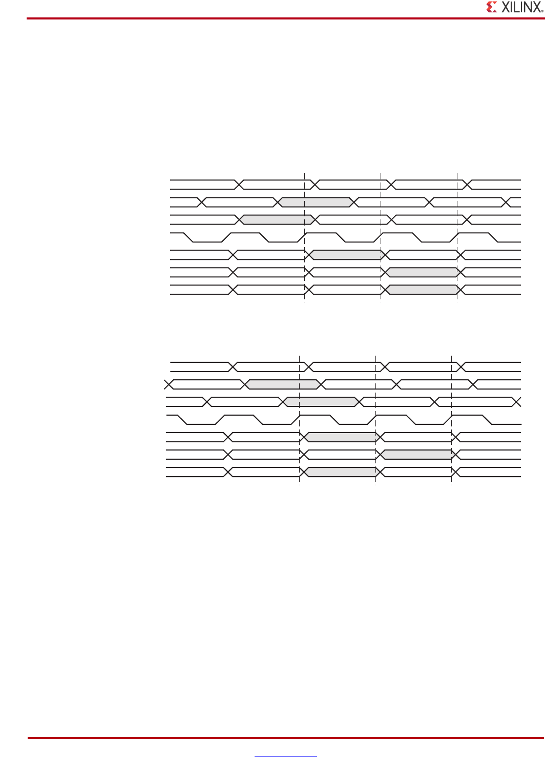
88 www.xilinx.com Spartan-6 FPGA SelectIO Resources
UG381 (v1.7) October 21, 2015
Chapter 3: Advanced SelectIO Logic Resources
The signals S3 and S2 give an indication of when the incoming data changes, and then by
using the E3 signal it can be determined whether the signal was sampled early or late. The
E3 sample is taken (nominally) half a clock cycle in time after the S3 signal, and so can take
one of two values. If the E3 sample is the same as S2, the S3 sample was taken early, and if
the E3 sample is the same as the S3 signal, the S3 sample was taken late. Since there is no
indication that the sample was taken at exactly the right time, it will, by definition, always
be identified as early or late. A timing diagram for the case where the sample was taken
early is shown in Figure 3-7, and the timing for when the sample is taken late is shown in
Figure 3-8.
The results of the comparison between S3, S2, and E3 either increment or decrement a
counter, which is reset to zero at each occurrence of the global clock. This is, for example,
every seven I/O clock periods if the SerDes factor is seven. When the clock occurs, if this
averaging counter is non-zero, then VALID is asserted, and INCDEC indicates the
direction that the master delay needs to be moved to center the I/O clock in the middle of
the incoming data bits and ensure correct data reception.
As the I/O sampling clock is always a single data rate clock, even if the incoming clock is
DDR or divided, the logic is all registered on the rising edges of this clock, and therefore
none of potential inaccuracies of double rate clocking (for example duty cycle distortion)
are applicable here if the PLL is used for multiplication. If an incoming DDR clock is used
through the BUFIO2_2CLK primitive to generate the single rate I/O clock, then any
incoming distortion on the DDR clock is transferred to the I/O clock, and effectively
appears as jitter. If the DCM is used with two global buffers, for example CLK0 and
X-Ref Target - Figure 3-7
Figure 3-7: Phase Detector Internal Timing for Early Data Sampling–Check for S3 ≠S2 and E3 = S3
Data via Master Input Delay
Data via Slave Input Delay
I/O Clock
S3
S2
E3 + One Stage of Pipeline
Data at Input Pin
ug381_c3_07_111913
D
n–1
D
n
D
n+1
D
n–1
D
n
D
n+1
D
n
D
n+1
D
n-1
D
n–1
D
n
D
n+1
D
n–1
D
n
D
n–1
D
n
X-Ref Target - Figure 3-8
Figure 3-8: Phase Detector Internal Timing for Late Data Sampling–Check for S3 ≠S2 and E3 = S3
Data via Master Input Delay
Data via Slave Input Delay
I/O Clock
S3
S2
E3 (No Pipeline Stage)
Data at Input Pin
ug381_c3_08_111913
D
n–1
D
n
D
n+1
D
n–1
D
n
D
n+1
D
n–1
D
n
D
n+1
D
n–1
D
n
D
n+1
D
n-1
D
n
D
n–1
D
n
D
n+1
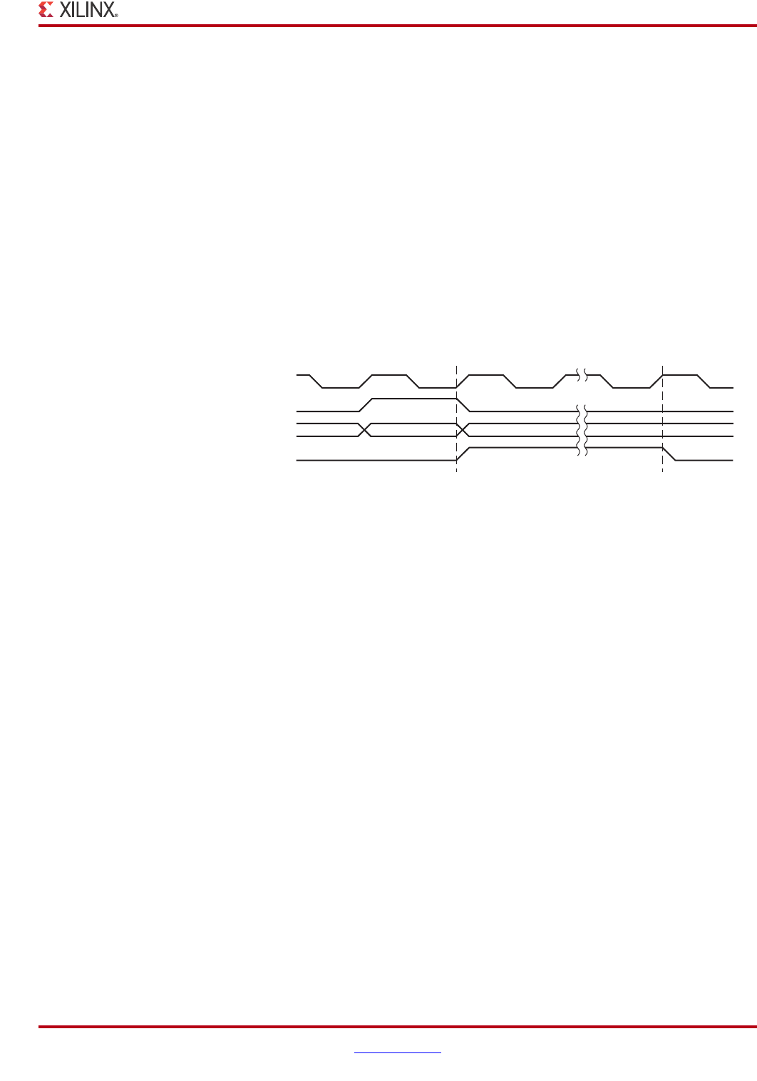
Spartan-6 FPGA SelectIO Resources www.xilinx.com 89
UG381 (v1.7) October 21, 2015
Phase Detector Overview
CLK180, then any slight mismatch in the global distribution of the clocks is also transferred
to the I/O clock and appears as jitter.
Delay Update and BUSY Timing
Each delay element also has a BUSY output which when deasserted indicates that the
delay element is ready for another command, either for calibration or to increment or
decrement the delay-line tap setting.
When the delay line is updated with a new value, as shown in the increment/decrement
example in Figure 3-9, this new value is not immediately operational. This is because valid
data reception still has to be guaranteed during the update process, so synchronization is
extremely important. Once the designer updates the delay values, the BUSY signal
transitions High indicating that synchronization is in progress, and does not return Low
again until four input data line transitions are received. Once BUSY is Low, the new value
can be assumed to be operational. In the absence of data transitions, BUSY therefore can
stay deasserted for long periods of time.
X-Ref Target - Figure 3-9
Figure 3-9: IODELAY2 Adjustment Timing
CE
INCDEC
BUSY
Global Clock
UG381_c3_09_111913
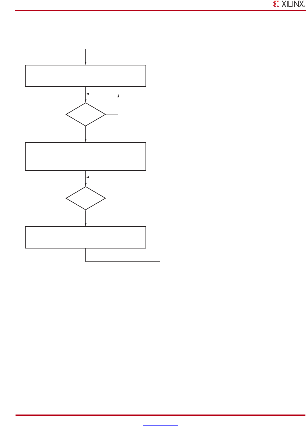
90 www.xilinx.com Spartan-6 FPGA SelectIO Resources
UG381 (v1.7) October 21, 2015
Chapter 3: Advanced SelectIO Logic Resources
The pseudo code for the operation of the phase detector function is shown in Figure 3-10.
d
X-Ref Target - Figure 3-10
Figure 3-10: Example State Machine Diagram
UG381_c3_10_111913
Power On or RESET
BUSY?
Issue CAL followed by RST commands to
both the MASTER and SLAVE input delays.
Master delay becomes half of MAX
Slave delay becomes zero
New Master delay becomes old Master delay, ±1
New Slave delay becomes new Master delay minus half of MAX.
If the new slave delay is greater than MAX or less than zero,
then delay wraparound will occur.
Master delay is unaffected
Slave delay becomes Master delay minus half of the new MAX.
If the new slave delay is greater than MAX or less than zero,
then delay wraparound will occur.
Periodically issue CAL commands
to the SLAVE input delay only.
BUSY?
Increment or Decrement both MASTER and
SLAVE input delays depending on the phase
detector results.
Spartan-6 FPGA SelectIO Resources www.xilinx.com 91
UG381 (v1.7) October 21, 2015
OSERDES2 Overview
Phase Detector Simulation
The design entry models for the IODELAY2 and the ISERDES2 are separate entities,
whereas in the silicon the two units are tightly coupled. For this reason, delays to the net
going from the slave IODELAY2 to the slave ISERDES2 can appear incorrect under certain
conditions. This is an unavoidable by-product of the modelling process, but the phase
detector outputs from the master ISERDES2 are correct in both simulation and silicon.
OSERDES2 Overview
Each IOB contains a output serializer block that can be instantiated in a design by using the
OSERDES2 primitive. OSERDES2 allows parallel-to-serial conversion with SerDes ratios
of 1:1 (SDR mode only), 2:1, 3:1, and 4:1. The SerDes ratio is the ratio between the high-
speed I/O clock that is transmitting data, and the slower internal global clock used for
processing the parallel data. For example, with an I/O clock running at 500 MHz to
transmit data at 500 Mb/s and a SerDes ratio of 4:1. If the SerDes ratio is 8:1 (using two
cascaded OSERDES2), then the parallel data clock would be 62.5 MHz. The OSERDES2
transfers four bits of data at one quarter of this rate (125 MHz) from the FPGA logic.
When using differential outputs, the two OSERDES2 primitives associated with the two
IOBs can be cascaded to allow higher SerDes ratios of 5:1, 6:1, 7:1 and 8:1.
OSERDES2 Ports and Attributes
Table 3-5 lists the available ports in the OSERDES2 primitive.
Table 3-5: OSERDES2 Port List and Definitions
Port Name Type Description
CLK0 Input I/O clock network input. Optionally invertible. This is the primary clock input used when
the clock doubler circuit is not engaged (see DATA_RATE attribute).
CLK1 Input I/O clock network input. Optionally invertible. This secondary clock input is only used
when the clock doubler is engaged (see DATA_RATE attribute).
CLKDIV Input Global clock network input. This is the clock for output data and control signals from the
FPGA logic domain.
IOCE Input
Data strobe signal derived from BUFIO2 or BUFPLL CE. Strobes data capture to be correctly
timed with respect to the I/O and global clocks for the SerDes mode selected. Reregistered
inside the OSERDES2.
D4, D3, D2, D1 Inputs Data inputs
OCE Input Clock enable for data inputs
RST Input Shared data, 3-state reset pin. Asynchronous only.
T1, T2, T3, T4 Inputs 3-state control inputs.
TCE Input Clock enable for 3-state inputs.
SHIFTIN1 Input Cascade data input signal (dummy in master). Used for DATA_WIDTHs greater than 4.
SHIFTIN2 Input Cascade 3-state input signal (dummy in master). Used for DATA_WIDTHs greater than 4.
SHIFTIN3 Input Differential data input signal (dummy in slave)
SHIFTIN4 Input Differential 3-state input signal (dummy in slave)
92 www.xilinx.com Spartan-6 FPGA SelectIO Resources
UG381 (v1.7) October 21, 2015
Chapter 3: Advanced SelectIO Logic Resources
Table 3-6 summarizes all the applicable OSERDES2 attributes. For more information on
applying these attributes in UCF, VHDL, or Verilog code, refer to the Xilinx ISE Software
Manual.
TRAIN Input
Enable use of the training pattern. The train function is a means of specifying a fixed output
pattern that can be used to calibrate the receiver of the signal. This port allows the FPGA
logic to control whether the output is that fixed pattern or the input data from the pins.
OQ Output Data path output to pad or IODELAY2. 0 when RST is asserted.
TQ Output 3-state path output to pad or IODELAY2.
SHIFTOUT1 Output Cascade data output signal (dummy in slave). Used for DATA_WIDTHs greater than 4.
SHIFTOUT2 Output Cascade 3-state output signal (dummy in slave). Used for DATA_WIDTHs greater than 4.
SHIFTOUT3 Output Differential data output signal (dummy in master)
SHIFTOUT4 Output Differential 3-state output signal (dummy in master)
Table 3-5: OSERDES2 Port List and Definitions (Cont’d)
Port Name Type Description
Table 3-6: OSERDES2 Block Attributes
Attribute Name Possible Values Default Value Description
DATA_RATE_OQ SDR, DDR DDR
Data rate settings. An SDR clock can be supplied
by a BUFIO2 clock, a BUFPLL clock, or a global
clock. A DDR clock can be supplied by two
separate BUFIO2 clocks or by one or two global
clocks.
DATA_RATE_OT SDR, DDR, BUF DDR
Data rate settings. An SDR clock can be supplied
by a BUFIO2 clock, a BUFPLL clock, or a global
clock. A DDR clock can be supplied by two
separate BUFIO2 clocks or by one or two global
clocks.
DATA_WIDTH [2 ... 8] 2
Data width. Determines the parallel data input
width of the parallel-to-serial converter. Values
greater than four are only valid when two
OSERDES2 blocks are cascaded. In this case, the
same value should be applied to both the master
and slave blocks.
OUTPUT_MODE SINGLE_ENDED,
DIFFERENTIAL SINGLE_ENDED
Output mode. Always set to SINGLE_ENDED
for both single-ended and true differential
output standards. Set to DIFFERENTIAL only in
the case of an OSERDES2 in SLAVE mode when
used to drive a pseudo-differential output
standard such as DIFF_SSTL18_I.
SERDES_MODE NONE, MASTER, SLAVE NONE
Indicates whether OSERDES2 is being used
alone, or as a master or slave when two
OSERDES2 blocks are cascaded.
TRAIN_PATTERN [0 ... 15] 0 Defines training pattern to be sent when TRAIN
port is active.
Spartan-6 FPGA SelectIO Resources www.xilinx.com 93
UG381 (v1.7) October 21, 2015
OSERDES2 Overview
OSERDES2 Operation
The logic contained in the OSERDES2 is shown in Figure 3-11. Parallel data is received
from the FPGA logic and is clocked into a 4-bit register (A) by the associated global clock.
The four bits of parallel data are then transferred, using the I/O clock and the incoming
SerDes strobe signal, into a parallel-in serial-out shift register (B). Data in this register is
then passed serially to the output pin using the I/O clock. For example, timing only
becomes an issue when a SerDes ratio is:
• 2:1 (=DDR), where the I/O speed is limited to 500 Mb/s
• 3:1, where the I/O speed is limited to 750 Mb/s
All other SerDes ratios support the full data rate as specified in the data sheet.
Table 3-7 summarizes the interconnection pins shown in Figure 3-11 and the
corresponding OSERDES2 port name.
Table 3-7: Interconnection Pins When Cascading OSERDES2s
Interconnection Pin Description OSERDES2 Port Name
D Parallel Cascade In SHIFTIN1
T Parallel Cascade In SHIFTIN2
D Pin Cascade In SHIFTIN3
T Pin Cascade In SHIFTIN4
D Parallel Cascade Out SHIFTOUT1
T Parallel Cascade Out SHIFTOUT2
D Pin Cascade Out SHIFTOUT3
T Pin Cascade Out SHIFTOUT4
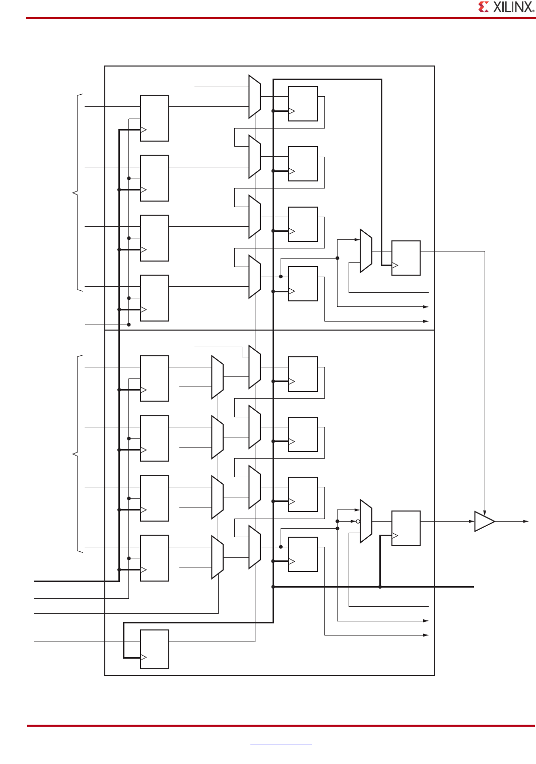
94 www.xilinx.com Spartan-6 FPGA SelectIO Resources
UG381 (v1.7) October 21, 2015
Chapter 3: Advanced SelectIO Logic Resources
X-Ref Target - Figure 3-11
Figure 3-11: Overview of OSERDES2 Block
ug381_c3_11_111913
Parallel
3-state
inputs
from
FPGA
logic
AB
D
CE
D
D
CE
D
CE
D
T4
T3
T2
T1
TCE
CE
Global Clock I/O Clock
To Pin
3-state Data
Output
Data
T Parallel Cascade In
Train(3)
T Pin Cascade In
T Parallel Cascade Out
T Pin Cascade Out
OCE
Parallel
data
inputs
from
FPGA
logic
D
CE
D
CE
Train(2)
Train(1)
Train(4)
Train
D
CE
D
D4
D3
D2
D1
CE
D
D
D
D
D Parallel Cascade Out
D
D Parallel Cascade In
D Pin Cascade In
D Pin Cascade Out
D
D
D
D
I/O Clock Enable
(SerDes Strobe) D
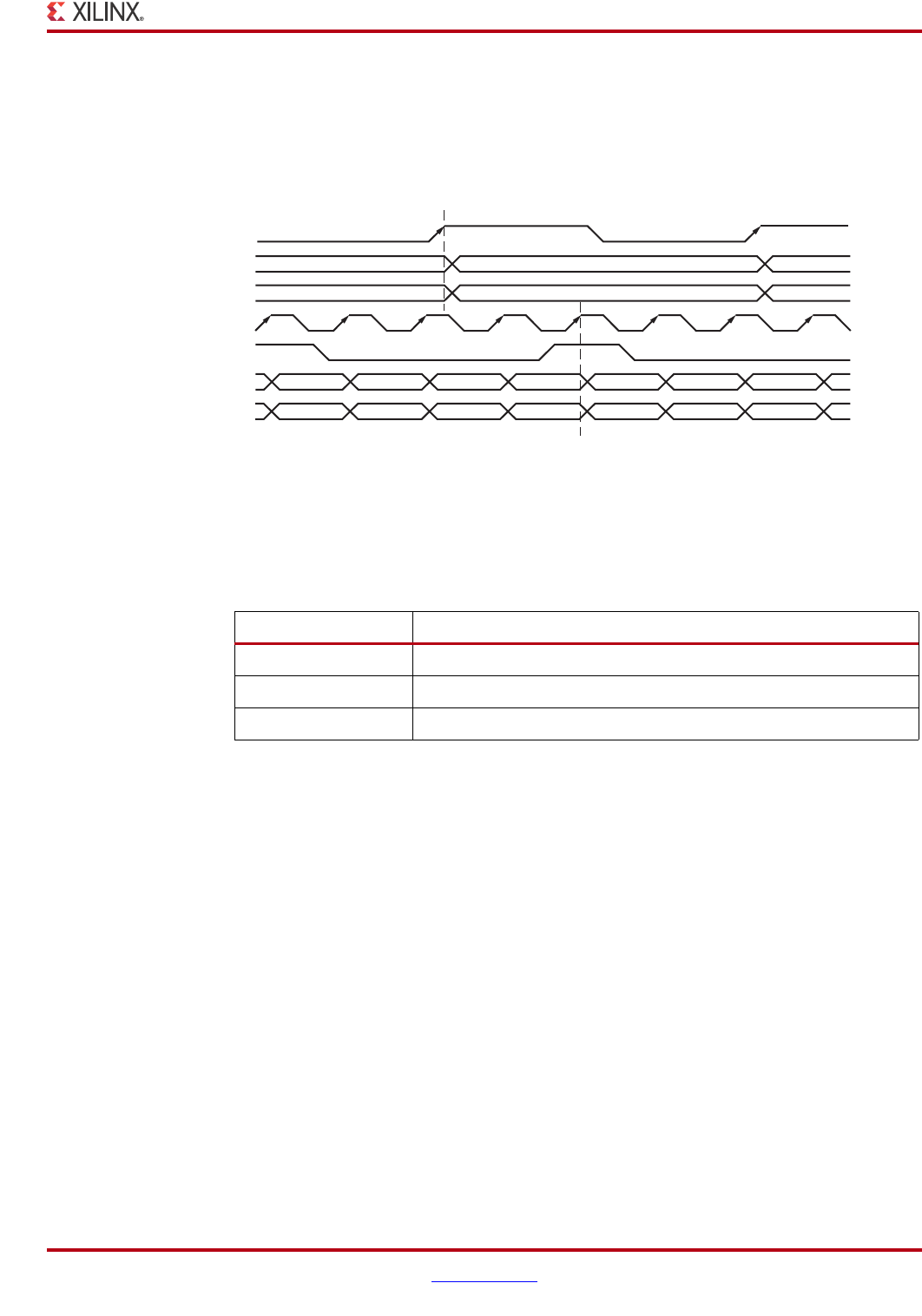
Spartan-6 FPGA SelectIO Resources www.xilinx.com 95
UG381 (v1.7) October 21, 2015
OSERDES2 Overview
The timing of the SerDes strobe ensures correct and loss-free transfer of data. The timing
diagram for operation, shown in Figure 3-12, assumes a 4:1 serialization is being
performed. The timing of the SerDes strobe is critical to achieving correct functionality.
This signal is generated either by a BUFIO2 or by a BUFPLL, both are described further in
the Spartan-6 FPGA Clocking Resources User Guide.
The valid data input pins from the FPGA logic for the various SerDes ratios available are
shown in Table 3-8. The T pins follow the same rules when 3-state functionality is required.
Cascade Operation
When using differential data transmission, the master OSERDES2 (associated with the
positive output pin) can be cascaded into the slave OSERDES2 (associated with the
negative output pin). This is achieved by connecting the relevant SHIFTOUT port of the
master OSERDES2 to the SHIFTIN port of the slave OSERDES2. These cascade connections
are shown in Figure 3-13 for the case of a true or pseudo-differential output.
X-Ref Target - Figure 3-12
Figure 3-12: OSERDES2 Timing Diagram (4:1 Illustrated)
Input Parallel Data
Parallel Register A
I/O Clock
Serdes Strobe
Parallel Register B
Serial Output Data
Global Clock
UG381_c3_12_111913
Table 3-8: Data Connections When Using a Single OSERDES2 Primitive With
Single-Ended Signalling
Output SerDes Factor Pins to Use for Output from the FPGA Logic (MSB–LSB)
2D2, D1
3 D3, D2, D1
4 D4, D3, D2, D1
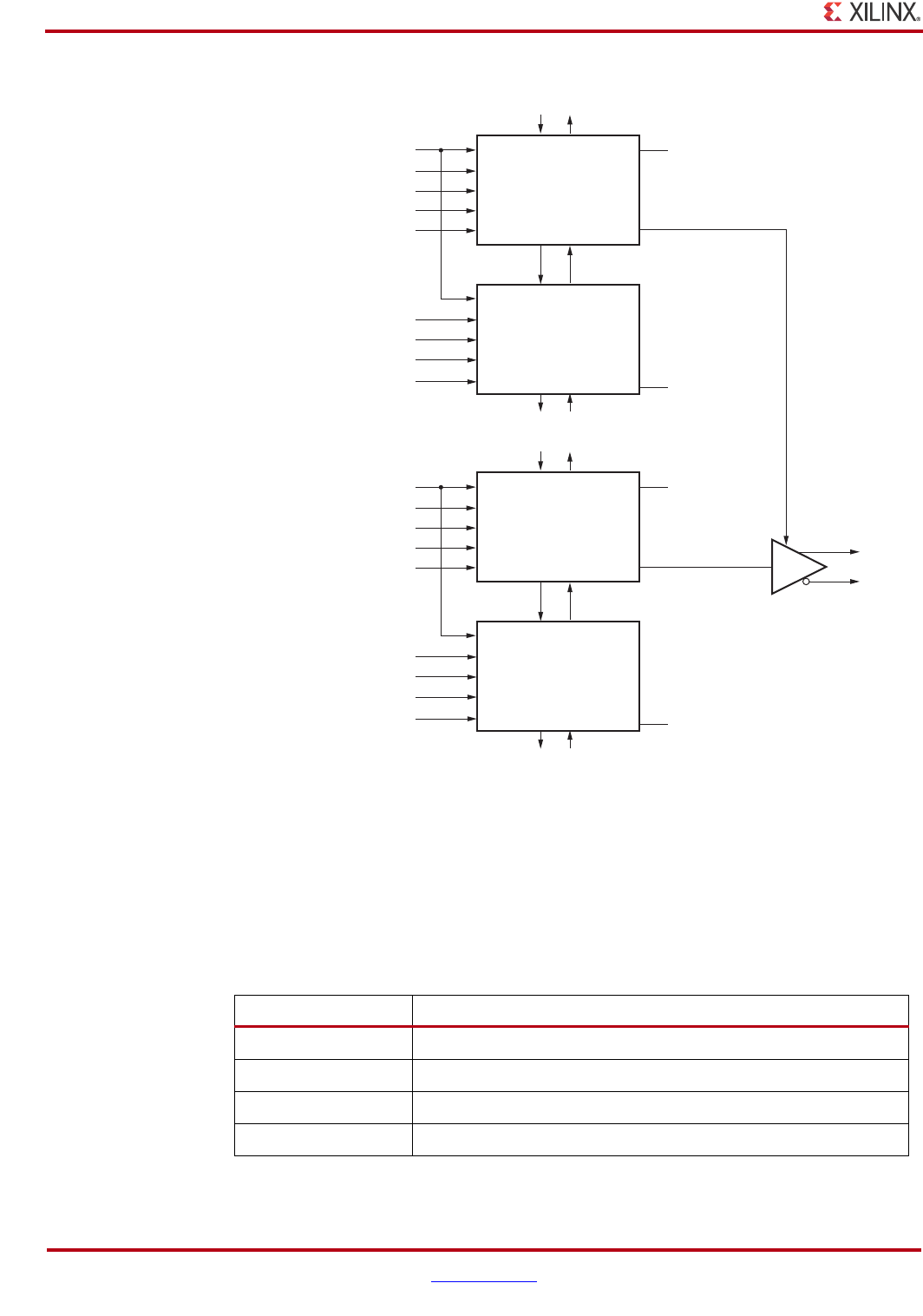
96 www.xilinx.com Spartan-6 FPGA SelectIO Resources
UG381 (v1.7) October 21, 2015
Chapter 3: Advanced SelectIO Logic Resources
The transmitted data now has access to both banks of flip-flops as before, but in the
cascaded case, each bank is effectively comprised of eight flip-flops. The SerDes strobe is
modified accordingly using the BUFPLL or BUFIO2 attributes.
The valid output pins for the various SerDes ratios available are shown in Table 3-9. The
T pins follow the same rules when 3-state functionality is required.
X-Ref Target - Figure 3-13
Figure 3-13: Connecting OSERDES2 Blocks Configured as 8:1 with a
Differential Output
Table 3-9: Data Connections When Cascading Two OSERDES2 Primitives
Output SerDes Factor Pins to Use for Output from the FPGA Logic (MSB–LSB)
5 Master (D1) and Slave (D4, D3, D2, D1)
6 Master (D2, D1) and Slave (D4, D3, D2, D1)
7 Master (D3, D2, D1) and Slave (D4, D3, D2, D1)
8 Master (D4, D3, D2, D1) and Slave (D4, D3, D2, D1)
ug381_c3_13_111913
Master T
Shift Register
Slave T
Shift Register
OBUFDS
T Pin Cascade
SHIFTIN4SHIFTOUT2
SHIFTOUT4SHIFTIN2
SHIFTIN4SHIFTOUT2
SHIFTOUT4SHIFTIN2
TQ
T Cascade
Clock Enable TCE
Last Bit Transmitted
First Bit Transmitted
Parallel 3-state inputs
from FPGA logic
1
Master D
Shift Register
Slave D
Shift Register
D Pin Cascade
SHIFTIN3SHIFTOUT1
SHIFTOUT3SHIFTIN1
SHIFTIN3SHIFTOUT1
SHIFTOUT3SHIFTIN1
OQ
D Cascade
Clock Enable OCE
Last Bit Transmitted
First Bit Transmitted
Parallel date inputs
from FPGA logic
1
1
1

Spartan-6 FPGA SelectIO Resources www.xilinx.com 97
UG381 (v1.7) October 21, 2015
OSERDES2 Overview
Training Feature Overview
Each OSERDES2 includes a training feature that enabled by using the TRAIN input on the
OSERDES2 primitive synchronous to the global clock.
When asserted, TRAIN forces the OSERDES2 to transmit a fixed bit pattern (set during
design) using the TRAIN_PATTERN attribute on the OSERDES2 primitive, and to ignore
the incoming parallel data.
This feature is used in systems where a training pattern is required to be sent at regular
intervals.