340S8 Service Manual Uniwill
User Manual:
Open the PDF directly: View PDF ![]() .
.
Page Count: 83
Chapter 5 Troubleshooting Guidelines
340S8 Rev : A Page
1
1.1 System features
1.1.1 General features
a. Support cost efficient CPU,
- Celeron-128K Socket 370 Type FCPGA 500~700 MHz
- Pentium III Socket 370 Type FCPGA 500~1.0GHz
b. Superior portability with all in one design
c. Support high quality audio include 2 internal high power speaker
d. Fully Support ACPI 1.0, meet PC98/PC99 requirement
e. Built-in 56K modem for Data/Fax/Voice modem or Internet (optional)
f. Support high performance hardware 2D/3D graphic engine

Chapter 5 Troubleshooting Guidelines
340S8 Rev : A Page
2
g. Support high capacity memory up to 256 MB
h. Support one most flexibility of 32-bit Cardbus slot and PCMCIA card
1.1.2 Hardware specification
A. CPU:
Celeron-128K 500MHz to 700MHz
• System bus frequency at 66 MHz
• Dynamic execution micro-architecture
• MMX technology capability
• Optimized for 32 bits AP and OS
• Power Management capability
• Integrated 32KB instruction and data L1 cache
• Integrated 128 KB instruction and data L2 cache
Pentium III 500MHz and 1.0 GHz
• System bus frequency at 100MHz / 133MHz
• On-die 256KB L2 advanced transfer cache with ECC
• Dual independent bus architecture
• SIMD extensions for enhanced video, sound and 3D performance
• Dynamic execution micro architecture
• Power management capability
• Optimized for 32bits AP and OS
• Integrated 16KB instruction and 16KB data L1 cache
• 256bit cache data bus
• 8-way cache associatively
• ECC for system bus data
B. Core Logic
SIS 630S
• Integrated North Bridge, advanced hardware 2D/3D GUI engine, Super South
Bridge and a 4X AGP internal
• Integrated Ultra AGP technology and advanced 64-bit graphic display interface
and delivers AGP 4X performance and Fast Write transactions
• Provides powerful hardware decoding DVD accelerator to improve DVD
playback performance.
• Provides standard interface between PC and a digital flat panel monitor.
• Adopts Share System Memory Architecture which the Super South Bridge in
SIS 630S integrates all peripheral controllers /accelerators /interfaces
• Provides total communication solution including 10/100MB Fast Ethernet
• Offers AC’97 compliant interface that comprises digital audio engine with 3D-
hardware accelerator, on-chip full duplex sample rate converter
• Provides interface to Low Pin Count (LPC) operating at 33MHz clocks which
is the same as the PCI clock on the Host.
• Built-in fast PCI-IDE controller supports the ATA PIO/DMA and
ultraDMA33/66/100 functions that supports the data transfer rate up to 100
MB/s

Chapter 5 Troubleshooting Guidelines
340S8 Rev : A Page
3
C. PCMCIA Controller
O2 Micro OZ6812
• ACPI-PCI bus power management interface specification Rev.1.0 compliant
• Compliant with PCI specification V2.1S, 1995 PC Card Standard and JEIDA
4.1
• Supports PCMCIA ATA specification
• Supports 5V/3.3V PC Cards and 3.3V Cardbus Cards
• Supports single PC card or Cardbus slot with hot insertion and removal
• Supports multiple FIFOs for PCI/CB data transfer
• Supports Direct memory access for PC/PCI and PC/Way on PC Card socket
• Win98IRQ and PC-97/98 compliant
• Integrated PC98 Subsystem Vendor ID support with auto lock bit
D. Embedded Controller / Keyboard Controller
NS PC87570
• Hot key for brightness, volume control
• ACPI controller
• SMB bus for smart battery
• Support Win-95 defined 3 new keys and down load-able key-matrix
E. Super I/O Controller
NS PC87393
• LPC System Interface with synchronous cycles, up to 33 MHz bus clock
• PC99 and ACPI Compliant
• Floppy Disk Controller (FDC)
• Support SPP, EPP and ECP Parallel port
• Software compatible with the 16550A and the 16450 serial port
• HP-IR, ASK-IR, Fast-IR support
F. Clock Generator
Realtek W83194R-63S
• Multiple CPU clocks for SDRAM architecture
• Provide power down mode in slowing down CPU clock
• Spectrum modulation reduce EMI
• Provide programmable clocks
• 166MHz Clock Support
1.2 System Specification
1.2.1 System Board
The major components of the computer include the system board, XGA color LCD
display, FDD module,CD-ROM module (24X rotational speed max) / DVD
module, keyboard, built-in glide pad with 2 click buttons, Lithium-ION battery
pack, and AC adapter.
The system board incorporates CPU module, system memory, system and VGA
BIOS, audio controller, CPU/ PCI bus controller, PCI / ISA bus controller. The
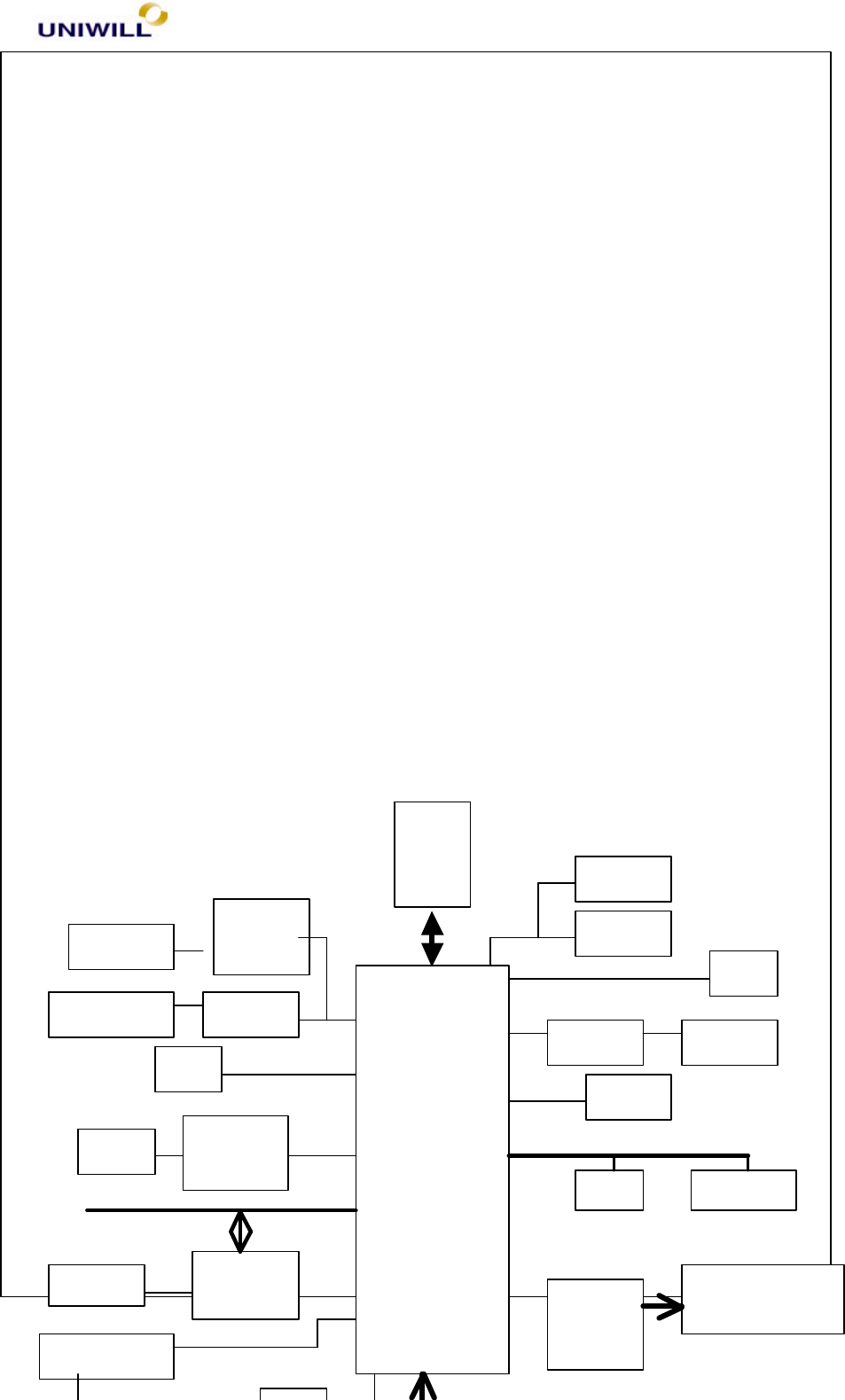
Chapter 5 Troubleshooting Guidelines
340S8 Rev : A Page
4
System Block Diagram shows how these components are integrated as shown in
the next page.
CPU
Sock
et
370
Host Bus
Core Logic
SIS 630S
PCI
LPC
DIMM
2
Alc 200
DIMM
1
LM483
5
DS90C
F363A
CS9211
CR
T
PHY
RTL820
1
Moden
Conn.
RJ
-
45
TFT
LCD
DSTN
LCD
US
B
SMBu
s
CPU
POWE
R
PCMCI
A
OZ6812
SLOT
1
CD
-
ROM
HD
D
RT
Cpu_core,+1.8
V,+2.5V,Vcc_c
mos

Chapter 5 Troubleshooting Guidelines
340S8 Rev : A Page
5
1.2.2 LCD Display
14.1” TFT
13.3” TFT
12.1” TFT
1.2.3 Power Plans
Power Source Descriptions
+5V : 5V power source
+3V : 3.3V power source
+12V : 12V power source
CPU_Core : CPU Core power source.
For Celeron, the voltage is 2.0V
For Pentium III, it is 1.7V
+2.5V : 2.5V power source
+1.8V : 1.8V power source for SIS630 & CPU AGTL + termination
power source
KBVCCA : KBC AD/DA 3.3V reference voltage
RTCVDD : Real time clock power source
+5V_AUX : LAN 5V always power source
+3V_AUX : LAN 3.3V always power source & KBC 3.3V power
Source
+3V_RX_TR : LAN 3.3V analog power source
Chapter 5 Troubleshooting Guidelines
340S8 Rev : A Page
6
+3V_TX_TR : LAN 3.3V analog power source
LCDVCC : LCD display 3.3V power source
VIN : Inverter 8~20V power source
ADAP+ : 20V Power supply from AC adapter
AMPVDD : 5V analog power for audio
1.2.4 Power Source Status
5V 3.3V 12V CPU
_core VCC_
CMOS
2.5V 1.5V 1.8V
FULL-ON ON ON ON ON ON ON ON ON
SLEEP ON ON ON ON ON ON ON ON
STD OFF OFF OFF OFF OFF OFF OFF OFF
SOFT-OFF OFF OFF OFF OFF OFF OFF OFF OFF
1.2.5 DC/DC Board
The DC/DC (system power) can support +3.3V, +5V, +12V for the main system.
The DC/DC (CPU power) can support +1.3V~2.05V, +1.8V, +2.5V for the CPU.
1.2.6 AC-DC Adapter
Input Voltage : 100 ~ 240 ±10% AC
Input Frequency : 50 ~ 60 Hz ±3Hz
Input AC current : 1.5A max @ 90 VAC
Efficiency : Better than 80%
Inrush Current : 50A @ 115VAC, 100A @ 230VAC
Holdup Time : 5mS (minimum)
Output Voltage/Current : 20V / 3.0A
Output Load Regulation : ±5%
1.2.7 Inverter
Input Voltage : 8-22 VDC
Output Voltage : 620 Vrms @ 45~55KHz
Start Up Voltage : 1200 Vrms (min.)
Brightness Adjust Range (tube current) : 3mA rms – 5.5mA rms
Protection : Open circuit protect, current limit protect
1.2.8 Battery Pack
A. Lithium – Ion Battery packs
• Battery type : Li-Ion
• Battery cells : 8 cells
• Battery Spec : 3.7V / 1800mAH
Chapter 5 Troubleshooting Guidelines
340S8 Rev : A Page
7
• Battery power : 47.36 watts (total)
• Battery protection : over charge protect, over discharge protect, over
temperature protect, short protect, over current protect
B. Ni-MH battery packs
• Battery type : Ni MH
• Battery cells : 10 cells
• Battery specs : 12V, 3800 mAh
• Battery power : 45.6 watts (total)
• Battery protection : over charge protect, over discharge protect, over
temperature protect, short protect, over current protect
1.2.9 Memory Module
144 pins SO-DIMM, 3.3V, SDRAM
memory type = 1Mx16, 4Mx16, 16Mx16, 2Mx8, 8Mx8, 16Mx8
memory size = 16M, 32M, 64M, 128M,
memory clock = 66 MHz / 100MHz / 133MHz
Memory Configuration Table
DIMM 1 DIMM 2 Total
16M 0 16M
32M 0 32M
64M 0 64M
128M 0 128M
16M 16M 32M
16M 32M 48M
32M 32M 64M
16M 64M 80M
32M 64M 96M
64M 64M 128M
64M 128M 192M
128M 128M 256M
1.2.10 Interrupt Request Channel
Setting Hardware using the setting
00 System timer
01 Standard 101/102-Key Microsoft Natural Keyboard
02 Programmable Interrupt Controller
03 IrDA V3.0 Fast Infrared Port
04 Communications Port (Com1)
06 Standard Floppy Disk Controller
07 ECP Printer Port (LPT1)
Chapter 5 Troubleshooting Guidelines
340S8 Rev : A Page
8
08 System CMOS/ Real Time Clock (RTC)
09 ACPI IRQ Holder for PCI IRQ Steering
09 SiS 900 PCI Fast Ethernet Adapter
10 ACPI IRQ Holder for PCI IRQ Steering
10 HAMR 5600 Voice Modem
10 O2Micro OZ6812 CardBus Controller
10 SIS 7018 Audio Driver
11 ACPI IRQ Holder for PCI IRQ Steering
11 SIS 7001 PCI to USB Open Host Controller
11 SIS 7001 PCI to USB Open Host Controller
11 SCI IRQ used by ACPI bus
12 Microsoft PS/2 Port Mouse
13 Numeric data processor
14 SIS 5513 Dual PCI IDE Controller
14 Primary IDE Controller (dual FIFO)
15 Intel 82371AB/EB PCI Bus Master IDE Controller
15 Secondary IDE Controller (dual FIFO)
1.2.11 DMA Channel
Setting Hardware using the setting
01 IrDA V3.0 Fast Infrared Port
02 Standard Floppy Disk Controller
03 ECP Printer Port (LPT1)
04 Direct memory access controller
1.2.12 System LED Indicator
4 Num-lock (on/off)
4 Cap-lock (on/off)
4 Scroll-Lock (on/off)
4 FDD (on/off)
4 HDD (on/off)
4 CDROM (on/off)
4 Power (on/off)
When the system is powered on, the Power LED will be lighted on.
When ‘Battery Low Warning’ occurs, the Power LED will flash at a rate of
1 time every 16 second.
When ‘Battery Very Low Warning’ occurs, the Power LED will flash at a
rate of 1 time every 4 seconds if there is no ‘Suspend to Disk’ partition in
the hard disk.
4 Charge (flash/off): Will be flashing when the battery pack is being charged.
Chapter 5 Troubleshooting Guidelines
340S8 Rev : A Page
9
1.2.13 Hot Key:
Key combination Function
Fn + F1 (SMI) Standby Mode
Fn + F4 (SMI) Toggle LCD / CRT display
Fn + F5 (SMI) Volume increase
Fn + F6 (SMI) Volume decrease
Fn + F7 (SMI) Brightness up
Fn + F8 (SMI) Brightness down
Fn + F9 (SMI) Contrast up (for DSTN LCD)
Fn + F10 (SMI) Contrast down(for DSTN LCD)
UNIWILL COMPUTER CORP.
No.24, Pei Yuan Rd., Chung Li Industrial Park
Chung Li City, Taiwan, R.O.C.
TEL: 886-3-461-6000
FAX: 886-3-461-6317
URL: http:// www.uniwill.com.tw/
Chapter 5 Troubleshooting Guidelines
340S8 Rev : A Page
10
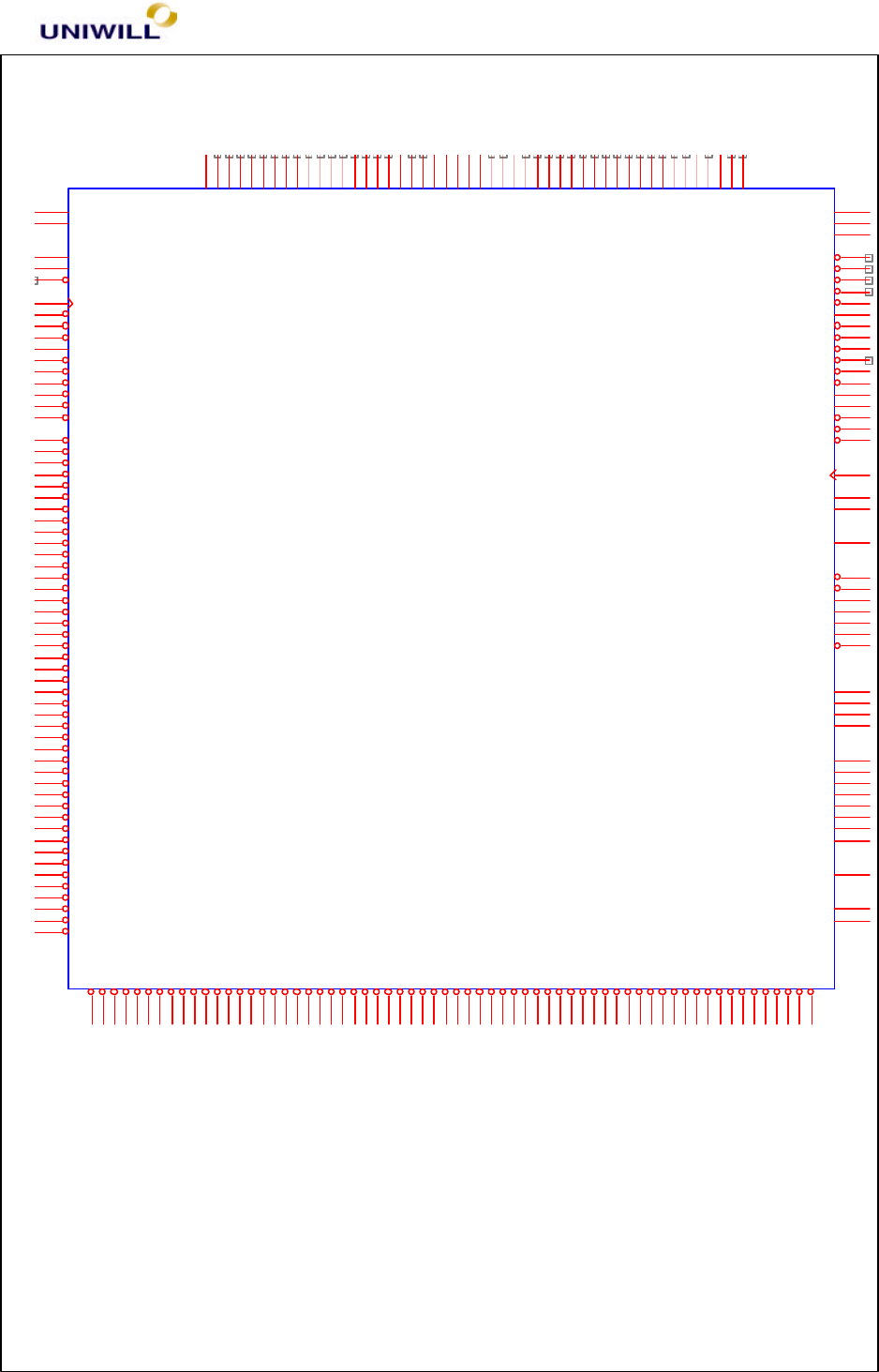
2.1 Connector Definitions
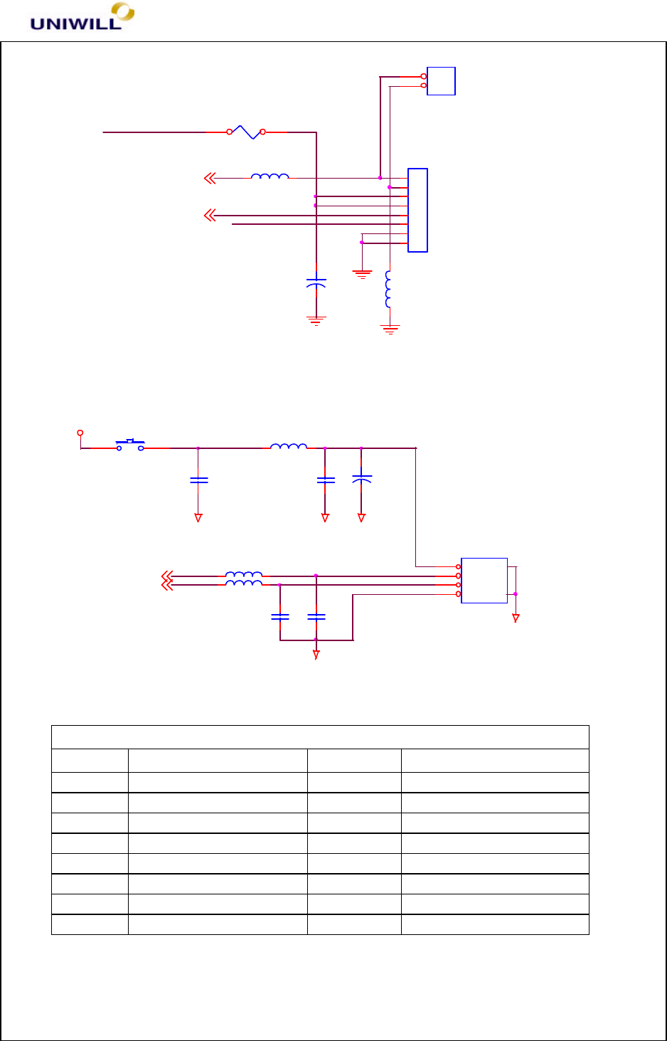
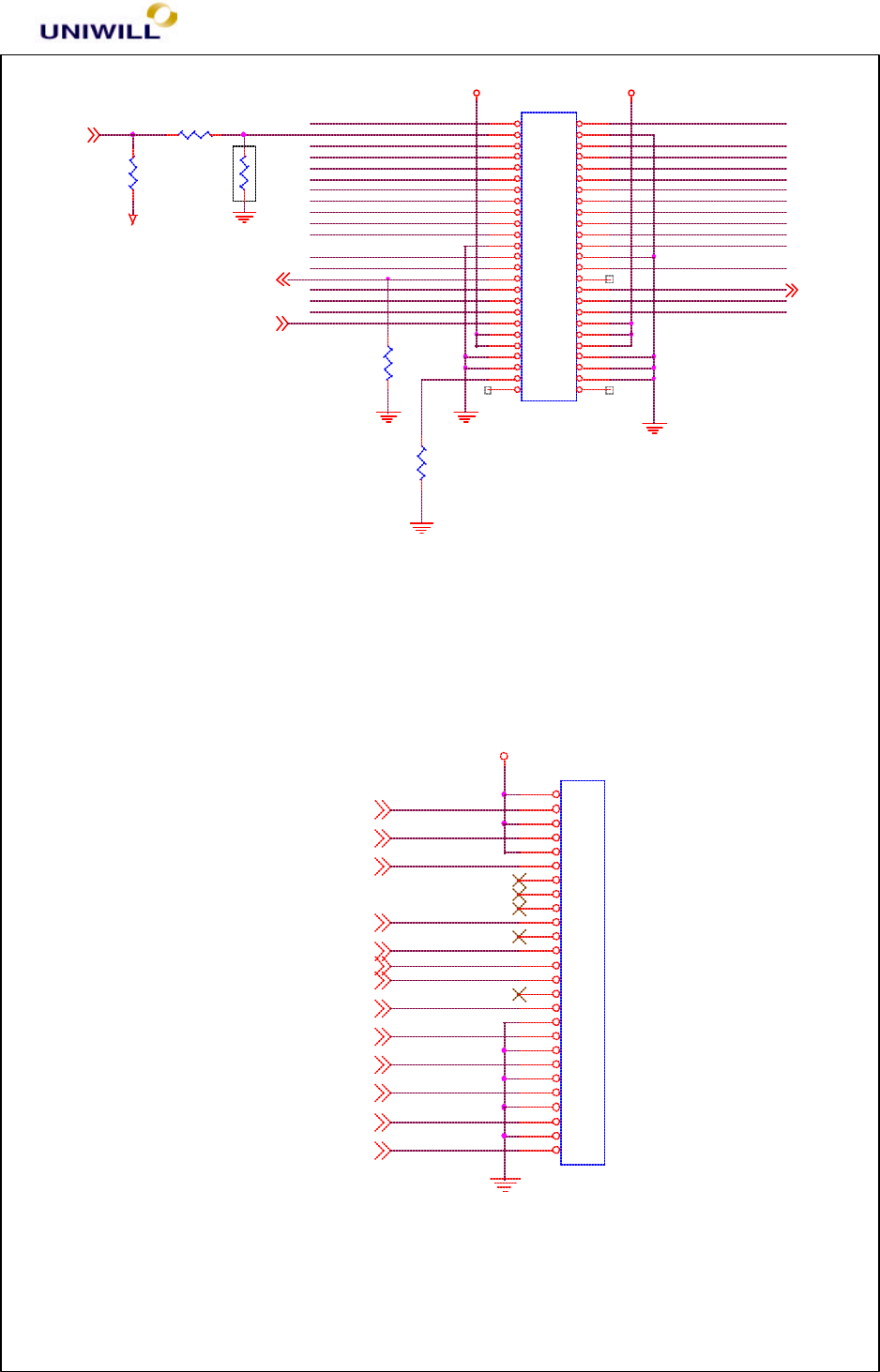
2.1.1 Memory DIMM144 Connector (CN5 and CN7)
2.1.2 MDC (Software Modem) Connector (CN27)
CN5
DIMM144
DQ0
3
DQ1
5
DQ2
7
DQ3
9
DQ4
13
DQ5
15
DQ6
17
DQ7
19
DQ8
37
DQ9
39
DQ10
41
DQ11
43
DQ12
47
DQ13
49
DQ14
51
DQ15
53
DQ16
83
DQ17
85
DQ18
87
DQ19
89
DQ20
93
DQ21
95
DQ22
97
DQ23
99
DQ24
121
DQ25
123
DQ26
125
DQ27
127
DQ28
131
DQ29
133
DQ30
135
DQ31
137
DQ32 4
DQ33 6
DQ34 8
DQ35 10
DQ36 14
DQ37 16
DQ38 18
DQ39 20
DQ40 38
DQ41 40
DQ42 42
DQ43 44
DQ44 48
DQ45 50
DQ46 52
DQ47 54
DQ48 84
DQ49 86
DQ50 88
DQ51 90
DQ52 94
DQ53 96
DQ54 98
DQ55 100
DQ56 122
DQ57 124
DQ58 126
DQ59 128
DQ60 132
DQ61 134
DQ62 136
DQ63 138
DQMB0/CAS0#
23
DQMB1/CAS1#
25
DQMB2/CAS2#
115
DQMB3/CAS3#
117
DQMB4/CAS4#
24
DQMB5/CAS5#
26
DQMB6/CAS6#
116
DQMB7/CAS7#
118
S0#/RAS0#
69
WE#
67
NU/OE#
73
SDA
141
SCL
142
A0 29
A1 31
A2 33
A3 30
A4 32
A5 34
A6 103
A7 104
A8 105
A9 109
A10 111
A11/BA0 106
VCC
11
VCC
27
VCC
45
VCC
63
VCC
81
VCC
101
VCC
113
VCC
129
VCC
143
VCC
12
VCC
28
VCC
46
VCC
64
VCC
82
VCC
102
VCC
114
VCC
130
VCC
144
VSS 1
VSS 21
VSS 35
VSS 55
VSS 75
VSS 91
VSS 107
VSS 119
VSS 139
VSS 2
VSS 22
VSS 36
VSS 56
VSS 76
VSS 92
VSS 108
VSS 120
VSS 140
S1#/RAS1#
71
A12/BA1 110
A13/A11 112
SRAS#/RFU
65
SCAS#/RFU
66
CKE0/RFU
62
CLK0
61
CLK1/RFU
74
RFU/A12 70
RFU/A13 72
CKE1/RFU
68
NC/CB0 57
NC/CB1 59
NC/CB2 77
NC/CB3 79
NC/CB4 58
NC/CB5 60
NC/CB6 78
NC/CB7 80
CN7
DIMM144-REV
DQ0
3
DQ1
5
DQ2
7
DQ3
9
DQ4
13
DQ5
15
DQ6
17
DQ7
19
DQ8
37
DQ9
39
DQ10
41
DQ11
43
DQ12
47
DQ13
49
DQ14
51
DQ15
53
DQ16
83
DQ17
85
DQ18
87
DQ19
89
DQ20
93
DQ21
95
DQ22
97
DQ23
99
DQ24
121
DQ25
123
DQ26
125
DQ27
127
DQ28
131
DQ29
133
DQ30
135
DQ31
137
DQ32 4
DQ33 6
DQ34 8
DQ35 10
DQ36 14
DQ37 16
DQ38 18
DQ39 20
DQ40 38
DQ41 40
DQ42 42
DQ43 44
DQ44 48
DQ45 50
DQ46 52
DQ47 54
DQ48 84
DQ49 86
DQ50 88
DQ51 90
DQ52 94
DQ53 96
DQ54 98
DQ55 100
DQ56 122
DQ57 124
DQ58 126
DQ59 128
DQ60 132
DQ61 134
DQ62 136
DQ63 138
DQMB0/CAS0#
23
DQMB1/CAS1#
25
DQMB2/CAS2#
115
DQMB3/CAS3#
117
DQMB4/CAS4#
24
DQMB5/CAS5#
26
DQMB6/CAS6#
116
DQMB7/CAS7#
118
S0#/RAS0#
69
WE#
67
NU/OE#
73
SDA
141
SCL
142
A0 29
A1 31
A2 33
A3 30
A4 32
A5 34
A6 103
A7 104
A8 105
A9 109
A10 111
A11/BA0 106
VCC
11
VCC
27
VCC
45
VCC
63
VCC
81
VCC
101
VCC
113
VCC
129
VCC
143
VCC
12
VCC
28
VCC
46
VCC
64
VCC
82
VCC
102
VCC
114
VCC
130
VCC
144
VSS 1
VSS 21
VSS 35
VSS 55
VSS 75
VSS 91
VSS 107
VSS 119
VSS 139
VSS 2
VSS 22
VSS 36
VSS 56
VSS 76
VSS 92
VSS 108
VSS 120
VSS 140
S1#/RAS1#
71
A12/BA1 110
A13/A11 112
SRAS#/RFU
65
SCAS#/RFU
66
CKE0/RFU
62
CLK0
61
CLK1/RFU
74
RFU/A12 70
RFU/A13 72
CKE1/RFU
68
NC/CB0 57
NC/CB1 59
NC/CB2 77
NC/CB3 79
NC/CB4 58
NC/CB5 60
NC/CB6 78
NC/CB7 80
Chapter 5 Troubleshooting Guidelines
340S8 Rev : A Page
11
2.1.3 SIS 630S Clock DIP Switch (SW3)
2.1.4 Inverter Connector (CN2) & MIC Connector (CN35)
+3V
BSEL1#1
BSEL0#1
Frequency Selection
10K
FS3
FS0
FS1
FS2
RP3
8P4RX4.7K
1
2
3
4 5
6
7
8
R67 10K
R68 10K
RP4
8P4RXR
1
2
3
4 5
6
7
8
SW3
DIP-SW
1
2
3
4
8
7
6
5
CPU PCI REF
66.6
100
33.3 14.318
SiS 630S CLOCK Select
133
W83194BR-63S
ICS9248-146(ICS)
ON
OFF
SDRAM
SW3
1 432
OFF OFF OFF
OFF OFF OFF
OFF OFF
OFF
OFF
OFF
ON ON
ON
ON
ON
ON
ON
ON
ON ON
ON ON
OFF OFF
OFF
OFF
OFF
OFF
OFF
66.6
66.6
66.6
66.6
100
100
100
100
100
133
133
133
133
33.3
33.3
33.3
33.3
33.3
33.3
33.3
14.318
14.318
14.318
14.318
14.318
14.318
14.318
CN27
MDC CON.
MONO_OUT
1
GND
3
AUXR
5
AUXL
7
CDGND
9
CD_R
11
CD_L
13
GND
15
3.3V
17
GND
19
3.3V
21
SDATA_O
23
RESET#
25
GND
27
MCLK
29 BCLK 30
GND 28
SDATA_INA 26
SDATA_INB 24
SYNC 22
GND 20
VCC 18
P_DN 16
R_D 14
R_D 12
VCC 10
GND 8
R_D 6
MONO_PHONE 4
AUDIO_PD 2
Chapter 5 Troubleshooting Guidelines
340S8 Rev : A Page
12
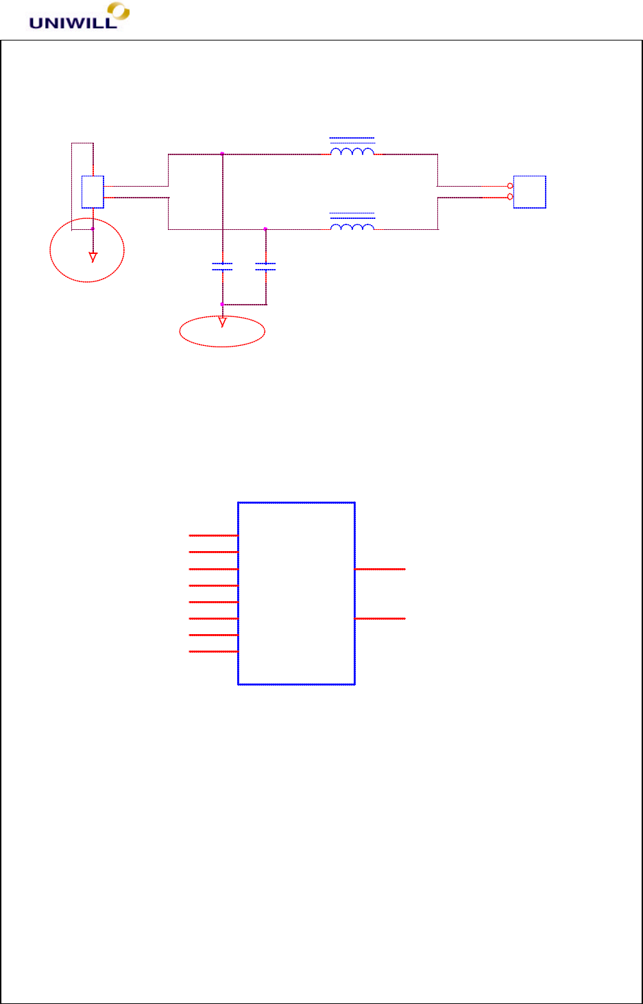
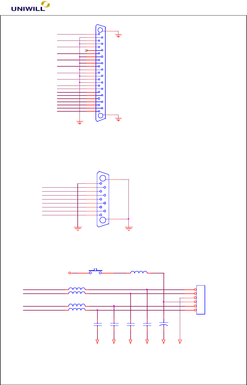
2.1.5 USB Connector (CN20)
2.1.6 CRT Connector (CN15)
Pin Description Pin Description
1 RED 9 +5V
2 GREEN 10 GND
3 BLUE 11 NC-
4 NC 12 DDCCLK
5 GND 13 HSYNC
6 DACGND 14 VSYNC
7 DACGND 15 DDCDATA
8 DACGND
2.1.7 Modem Phone (CN19) and Modem Connector (CN22)
INT_MIC11
BLTADJ17 DISPON
L59
BLM11P600S
CN2
INVERTER
1
2
3
4
5
6
7
8
L58
BLM11P600S
+C58
1u/25V
12
F1
3216FF/2A-1206
CN35
MIC CONN
1
2
+5V
USBGNDUSBGND
USBGND
USBGND
USBGND
USBP0+5USBP0-5
C36
47p
L57 BLM11P600S
L17 BLM11P600S
CN20
USB CONN
1
2
3
4
5
6
C239
47p
C267
0.1u
C230
1u
S3
POLY SW_1812
L62
BLM21300S_0805
+C97
150u/6V3_D3
12
Chapter 5 Troubleshooting Guidelines
340S8 Rev : A Page
13
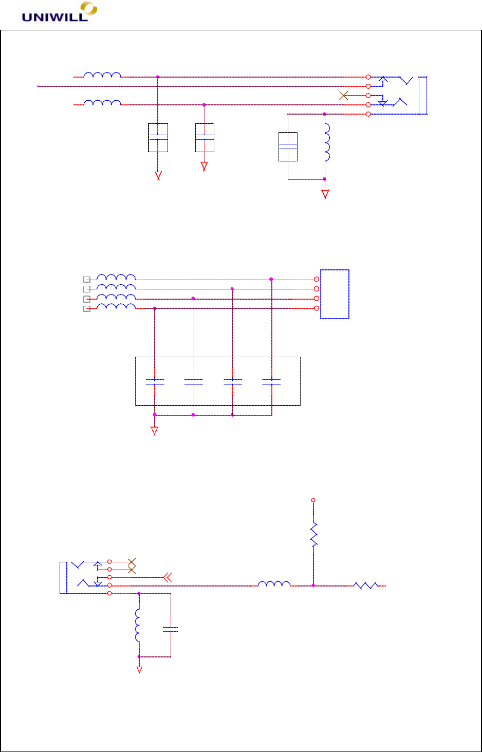
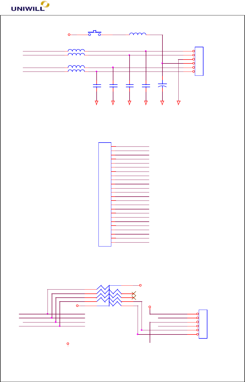
2.1.8 LAN - RJ45 Connector (CN16)
2.1.9 Speaker Jack (CN12)
USBGND
USBGND
MODEM
21-v60615-00
21-v60615-00
2KV
2KV
C246
1000p/2KV_1808
C255
1000p/2KV_1808
CN22
MODEM CONN
1
2
L82
60uH_SBT_0260_DIP
L83
60uH_SBT_0260_DIP
CN19
MODEM-PHONE
1
2
3
4
CN16
RJ45
TD+
1TD-
2RO+
3NC1
4NC2
5RO-
6NC3
7NC4
8
GND 9
GND 10
Chapter 5 Troubleshooting Guidelines
340S8 Rev : A Page
14
2.1.10 R/L Speaker Connector (CN3)
2.1.11 Microphone Jack (CN13)
2.1.12 PCMCIA Connector (CN28)
AUDGND
AUDGND AUDGND
0.1u
0.1u
0.1u
EXTSPKHP
EXTSPKL
EXTSPKR
L31
BLM11P600S
CN12
SPKR JACK
1
2
3
4
5
L35
BLM11P600S
L34
BLM11P600S C242
C
C234
CC548
C
AUDGND
R+
L-
L+
R-
CN3
R/L SPKR CONN
1
2
3
4
L2 BLM11P600S
L12 BLM11P600S
L13 BLM11P600S
L11 BLM11P600S
C30
C
C29
C
C32
C
C31
C
VREFOUT
AUDGND
INT_MIC 8
CN13
MIC JACK
1
2
3
4
5
R208
2K
R209
1K
L10
BLM11P600S
C27
680p
L9
BLM11P600S
Chapter 5 Troubleshooting Guidelines
340S8 Rev : A Page
15
2.1.13 HDD Connector (CN26)
2.1.14 CDROM Connector (CN23)
CN28
PCMCIA CONN
(D10) CAD31 66
(D9) CAD30 65
(D1) CAD29 31
(D8) CAD28 64
(D0) CAD27 30
(A0) CAD26 29
(A1) CAD25 28
(A2) CAD24 27
(A3) CAD23 26
(A4) CAD22 25
(A5) CAD21 24
(A6) CAD20 23
(A25) CAD19 56
(A7) CAD18 22
(A24) CAD17 55
(A17) CAD16 46
(IOWR*) CAD15 45
(A9) CAD14 11
(IORD*) CAD13 44
(A11) CAD12 10
(OE*) CAD11 9
(CE2*) CAD10 42
(A10) CAD9 8
(D15) CAD8 41
(D7) CAD7 6
(D13) CAD6 39
(D6) CAD5 5
(D12) CAD4 38
(D5) CAD3 4
(D11) CAD2 37
(D4) CAD1 3
(D3) CAD0 2
GND 68
GND 35
GND 34
GND 1
VCC
51
VCC
17
VPP
52
VPP
18
CCLK (A16)
19
CFRAME# (A23)
54
CIRDY# (A15)
20
CTRDY# (A22)
53
CDEVSEL# (A21)
50
CSTOP# (A20)
49
CPAR (A13)
13
CPERR# (A14)
14
CSERR# (WAIT*)
59
CREQ# (INPACK*)
60
CGNT# (WE*)
15
CINT# (IRQ*)
16
CBLOCK# (A19)
48
CCLKRUN# (IO16*)
33
CRESET# (RESET)
58
RFU (R2_D2)
32
RFU (R2_D14)
40
RFU (R2_A18)
47
CVS1
43
CVS2
57
CCD1# (CD1*)
36
CCD2# (CD2*)
67
CAUDIO (BVD2/SPKR*)
62
CSTSCHG (BVD1/RI*)
63
CC/BE3# (REG*)
61
CC/BE2# (A12)
21
CC/BE1# (A8)
12
CC/BE0# (CE1*)
7
69
70
71
72
73
74
75
76
V_HDDV_HDD
HDDLED#16
IRQ144CBLIDA 4
Primary Driver
PIDED1
PIDEA2
PIDEA1
PIDED11
PIDED9
PIDED13
HDDRST#
PIDED5
PIDED3
PIDED0
PIDEDREQ
PIORDY
PIDED8
PIDED10
PIDECS1#
PIDED2
PIDEA0
PIDED15
PIDECS3#
PIDEIOW#
PIDEDACK#
PIDED14
PIDEIOR#
PIDED12
PIDED7
PIDED6
PIDED4
R143
470R146
10K
CN26
HDD CONN
1 2
3 4
5 6
7 8
910
11 12
13 14
15 16
17 18
19 20
21 22
23 24
25 26
27 28
29 30
31 32
33 34
35 36
37 38
39 40
41 42
43 44
Chapter 5 Troubleshooting Guidelines
340S8 Rev : A Page
16
2.1.15 FDD Connector (CN10)
2.1.16 Parallel Connector (CN17)
V_CDROM V_CDROM
AUDGND
CD-ROMLED#16
IRQ154CBLIDB 4
CDGND11
Secondary Driver(Master)
Near to R106
SIDED9
SIDECDL
SIDED15
SIDEIOR#
SIDECDR
CDRST#
SIDED0
SIDED8
SIDEA1
SIDED4
SIDEA2
SIDED10
SIDEDREQ
SIDEIOW#
SIDED7
SIDED6
SIDEDACK#
SIDED3 SIDED13
SIORDY
SIDED2 SIDED14
SIDECS3#
SIDED12
SIDEA0
SIDED5 SIDED11
SIDECS1#
SIDED1
R49
10K
CN23
CDROM CONN
1 2
3 4
5 6
7 8
9 10
11 12
13 14
15 16
17 18
19 20
21 22
23 24
25 26
27 28
29 30
31 32
33 34
35 36
37 38
39 40
41 42
43 44
45
47
49
46
48
50
R62
470
R462 1K
R463
100K
R533
R
V_FDD
WDATA#14
TRK0#14
WGATE#14
WRPRT#14
3MODE#14
RDATA#14
STEP#14
HDSEL#14
MTR0#14
INDEX#14
DSKCHG#14
DRV0#14,16
FDIR#14
WRPRT#
TRK0#
RDATA#
DSKCHG#
INDEX#
CN10
FDD CONN
1
2
3
4
5
6
7
8
9
10
11
12
13
14
15
16
17
18
19
20
21
22
23
24
25
26
Chapter 5 Troubleshooting Guidelines
340S8 Rev : A Page
17
2.1.17 Serial Connector (CN18)
2.1.18 PS/2 Connector (CN14
2.1.19 PS/2 Connector (CN14)
LPTSLCT
LPTPE
LPTBUSY
LPTACK#
LPTD7
LPTD6
LPTD5
LPTD4
LPTD0
LPTD3
LPTSLCTIN#
LPTD2
LPTINIT#
LPTD1
LPTERR#
LPTAFD#
LPTSTB#
CN17
PARALLEL CONN
13
25
12
24
11
23
10
22
9
21
8
20
7
19
6
18
5
17
4
16
3
15
2
14
1
26
27
COMDCD1#
COMRTS1#
COMDSR1#
COMTXD1
COMDTR1#
COMRXD1
COMCTS1#
COMRI1
CN18
SERIAL CONN
5
9
4
8
3
7
2
6
1
10
11
+5V
USBGND
USBGND
USBGND
USBGND
USBGND
USBGND
PS2DATA
KBDATA
PS2CLK
KBCLK
C25
270p
L7
BLM11A221S
L6 BLM11A221S
C24
270p
CN14
PS2 CONN
1
2
3
4
5
6
C22
270p
L5 BLM11A221S
L4 BLM11A221S
C23
270p
S1
POLY SW_1812
+C231
1u
12
L8
BLM11P600S
Chapter 5 Troubleshooting Guidelines
340S8 Rev : A Page
18
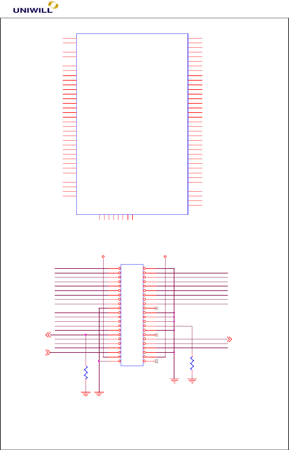
2.1.20 Internal KB Connector (CN8)
2.1.21 Touch Pad Connector (CN11)
+5V
USBGND
USBGND
USBGND
USBGND
USBGND
USBGND
PS2DATA
KBDATA
PS2CLK
KBCLK
C25
270p
L7
BLM11A221S
L6 BLM11A221S
C24
270p
CN14
PS2 CONN
1
2
3
4
5
6
C22
270p
L5 BLM11A221S
L4 BLM11A221S
C23
270p
S1
POLY SW_1812
+C231
1u
12
L8
BLM11P600S
SCANIN4
SCANOUT0
SCANOUT4
SCANOUT7
SCANOUT14
SCANOUT9
SCANOUT11
SCANOUT1
SCANIN5
SCANIN2
SCANIN7
SCANOUT5
SCANOUT8
SCANOUT12
SCANOUT15
SCANIN0
SCANOUT2
SCANIN6
SCANIN3
SCANOUT3
SCANOUT6
SCANOUT13
SCANOUT10
SCANIN1
CN8
INT KB CONN
1
2
3
4
5
6
7
8
9
10
11
12
13
14
15
16
17
18
19
20
21
22
23
24
+5V
+5V
+5V
KBVCC
PS2DATA PAGE_UP#
PAGE_DOWN#
KBCLK
KBDATA
PS2CLK
RN19
10P8RX10K
1
2
3
4
5
10
6
7
8
9
CN11
T/P CONN
2
3
4
1
5
6
Chapter 5 Troubleshooting Guidelines
340S8 Rev : A Page
19
2.1.22 Fan 1 (CN24) and Fan2 (CN25) Connector
2.2 Mechanical Buttons and Switch Definition
2.2.1 Power on/off button
1. If the system is in S0, S1 or S2 state, pressing the power button will transit the
system to S4 (Suspend to Disk) or S5 (Soft-off) state depending on the “Power
button function” setting in the BIOS Setup menu.
2. If the system is in S4 or S5 states, pressing the power button will awaken the system
into S0 states.
3. If the power button is pressed for more than four seconds, a power button over-ride
event is generated and the system will be put into S5 (Soft-off) state.
2.2.2 Cover (Lid) Switch
When LCD cover is closed, this Lid switch is triggered and an SMI/SCI is generated to
put the system into ‘Suspend to RAM’ or ‘Suspend to Disk’ mode depending on the
“Cover Switch” setting in the BIOS Setup menu.
2.2.3 Quick Start Button
When this button has been pressed, the system will launch either Microsoft Internet
Explorer, E-Support or E-mail/User Defines etc. 3 quick buttons demands.
2.3. Major Components and Connectors Location
+5V
CN25
FAN2 CONN
1
2
C385
0.1u
+5V
FANON#
Q36A
SI9953
1
2
7
8
C386
0.1u
CN24
FAN1 CONN
1
2
Q37
SI2301DS-SOT23
D
G
S
L89
BLM11P600S
Chapter 5 Troubleshooting Guidelines
340S8 Rev : A Page
20
2.3.1 Top Side
2.3.2 Top Side
BIOS
K/B conn.
CN11
T/P conn.
SiS 630S
CN5 -Memory socket # 1
Memory socket #2
CN10
FDD conn.
CN3
LID switch conn.
SPEAKER
conn.
LEDs
Power
SW -
SW6WWW
switch
SW 1
LCD
connectors
CN8
U17
CN31
CN2
O2 -
Micro
U22
PC87570-ICC/
VPC
PC87393
VJG
U19
U14
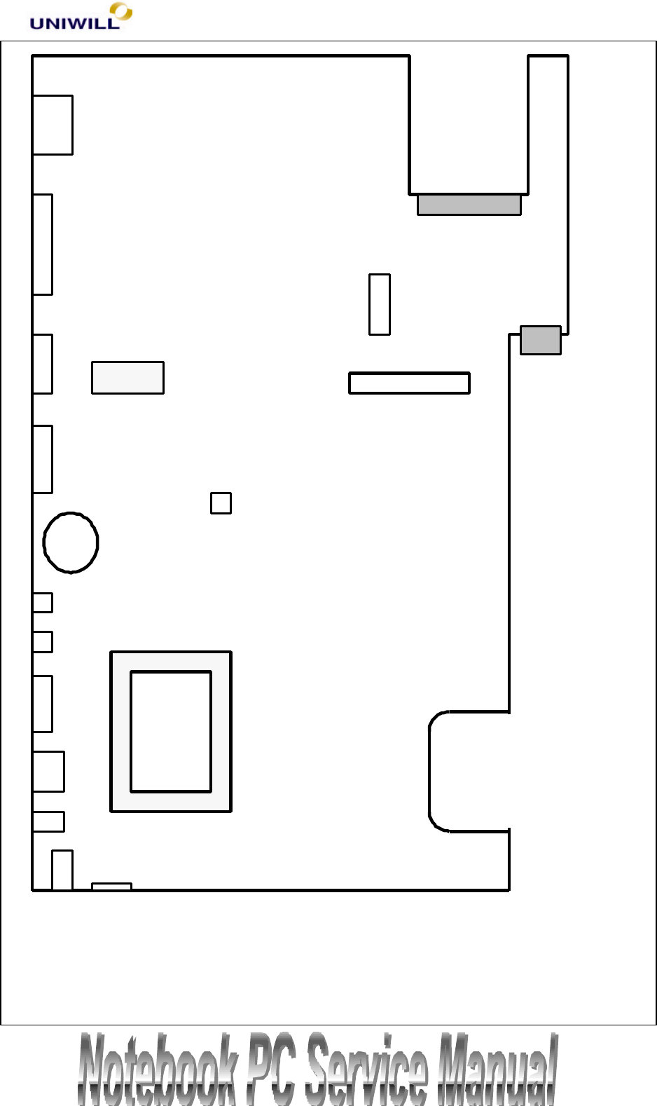
Chapter 5 Troubleshooting Guidelines
340S8 Rev : A Page
21
e
CN14 CN16
CN17CN18CN15
CMOS
Batt.
U 24
CPU SOCKET
CN
29
C
N
23
C
N
2
6
CD-ROM
connector
HDD
connector
C
N
2
8
PCMCIA
SLOT
CN27
MODEM
connector
Battery
connector
LAN
conn.
Printer
conn.
COM 1
ext.
CRT
conn
PS/2
conn
Modem
conn.
DC-IN
I R
MIC
CN12
ext.
spkr
CN13
CN 24
CPU FAN
conn.
USB
conn
Chapter 5 Troubleshooting Guidelines
340S8 Rev : A Page
22
UNIWILL COMPUTER CORP.
No. 24, Pei Yuan Rd., Chung Li Industrial Park
Chung Li City, Taiwan, R.O.C.
TEL: 886-3-461-6000
FAX: 886-3-461-6317
URL: http://www.uniwill.com.tw/
Chapter 5 Troubleshooting Guidelines
340S8 Rev : A Page
23
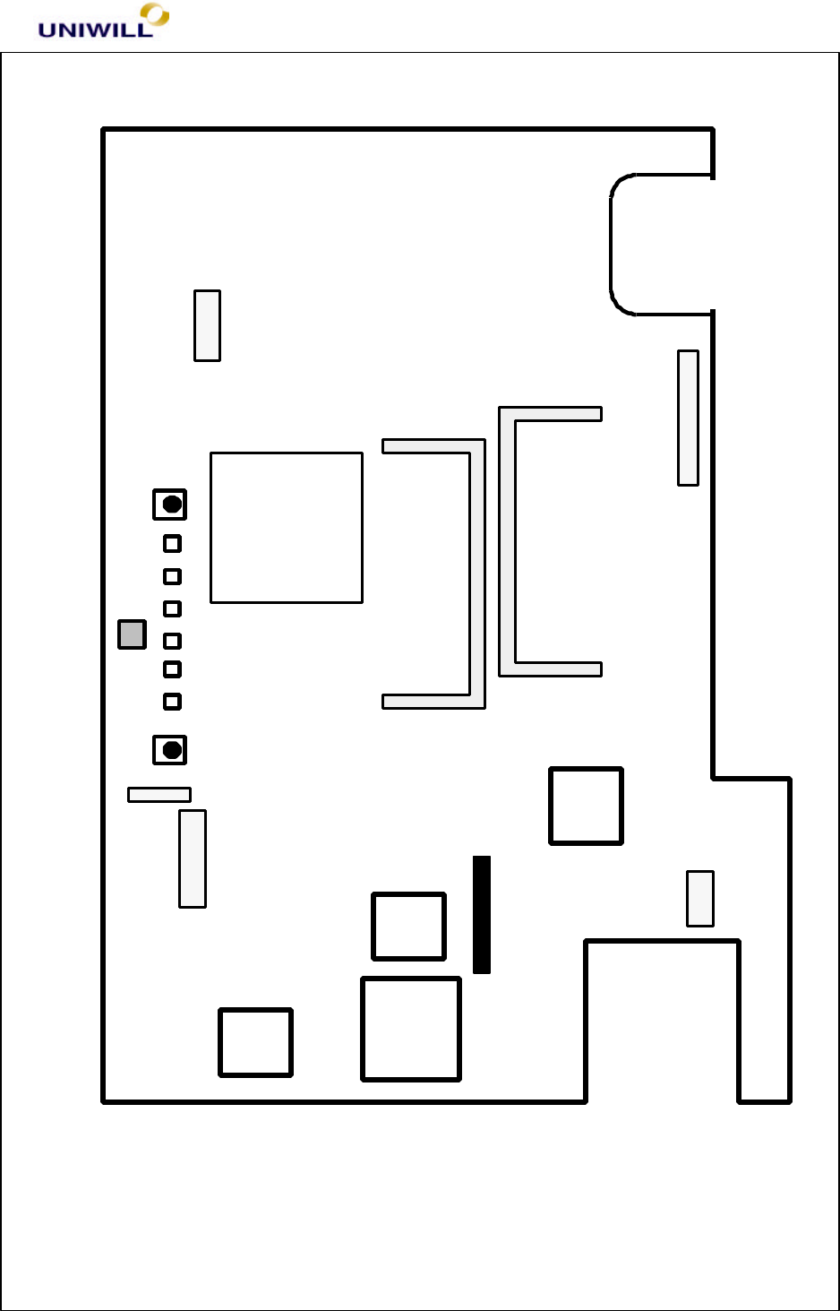
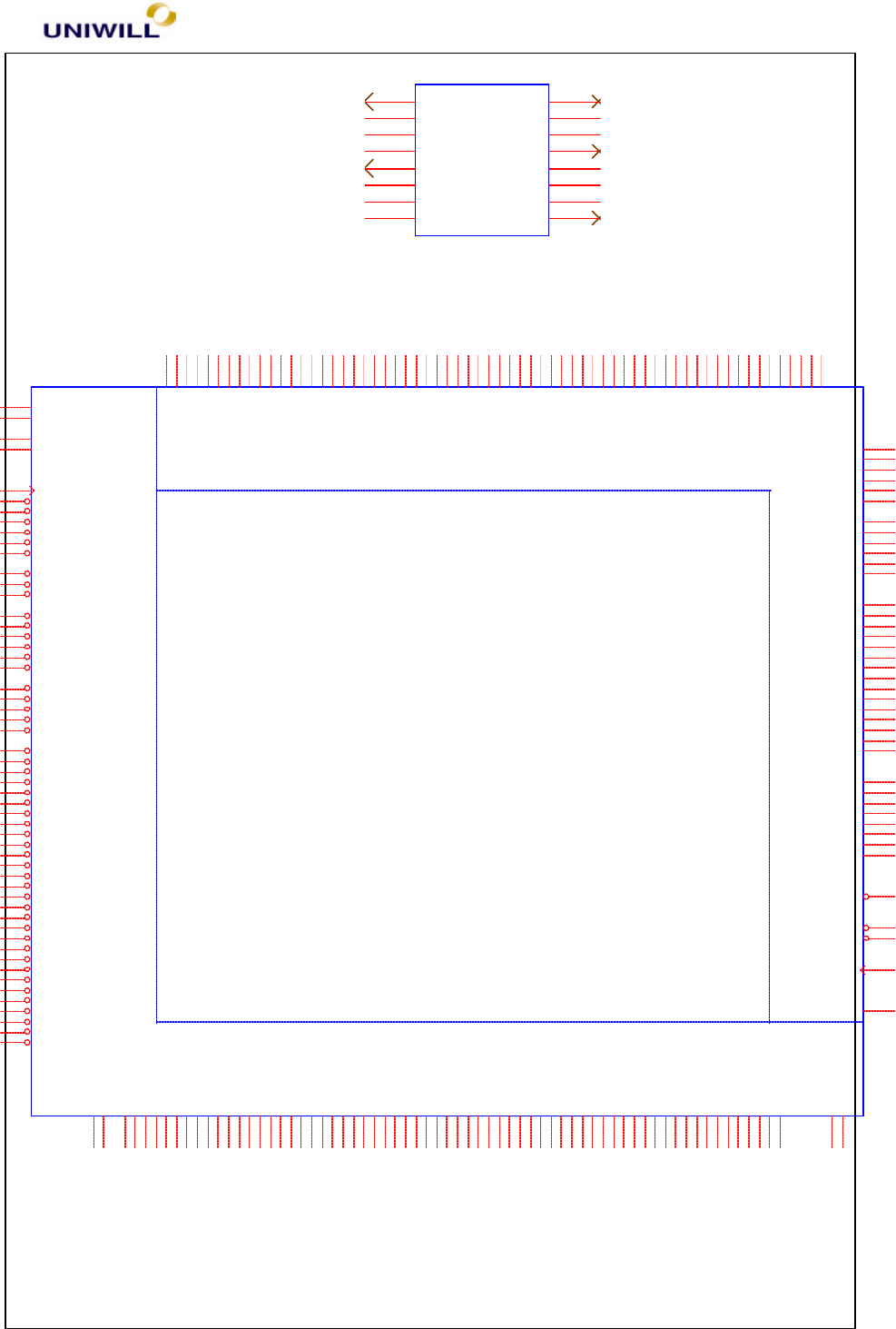
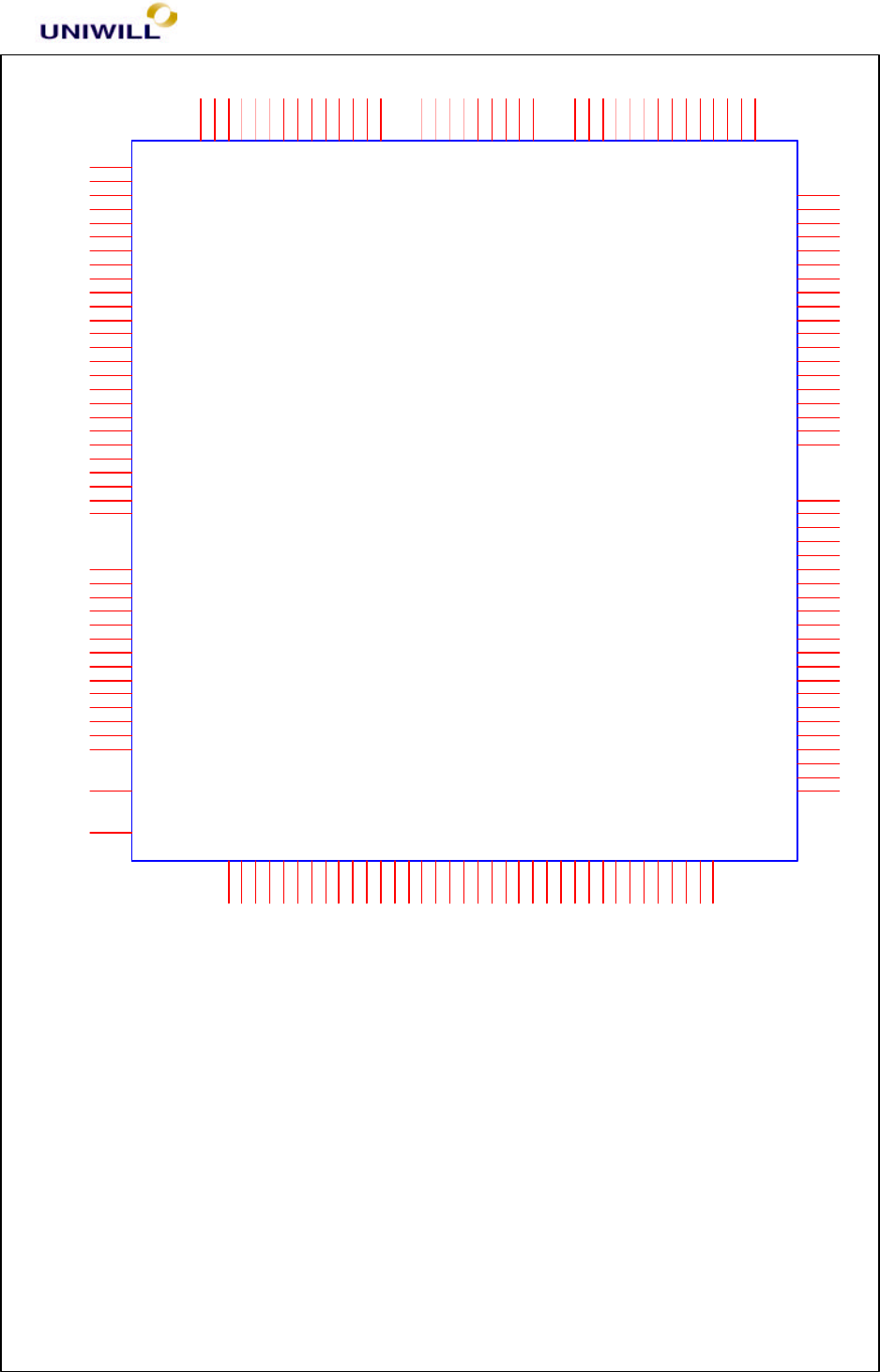
3.1 Major Component List
Reference
Component Part Number
U1 IC ALC-200 LQFP 02-U10002-30
U2 IC RTL8201 LQFP48P PHY 02-F82010-40
U3 IC GD75232 SOP20P RS-232 03-E75232-60
U4 IC LM4835 TSSOP-28 08-U00057-0U
U6 IC ADM1021 16 PIN QSOP 08-U10025-00
U8 IC DS90C363A TSSOP48P LVDS 03-F90363-95
U10 SIS 630S BGA 762 PIN MULTI-FUNCTION 02-A63001-A0
U11 IC SN74LVC14 14 PIN (T1) 07-U32037-00
U12 IC 74LVC08 QUAD 2 – INPUT 07-U32038-00
U13 IC 74LVC 32 0.65mm TSSOP -14P 07-U32057-00
U14 IC PC87393 TQFP 100 LPC-SUPERI/O 02-U50004-00
U18 IC ICS9248 –146 SSOP48P CLK GEN 03-A92481-70
U19 IC PC 87570 K/B AND POWER
MANAGEMT 02-U60001-00
U20 IC TC7SH32FU SINGLE 2 -INPUT 07-U81024-00
U21 IC MIC256A SO-14 9MICREL) 08-U10032-00
U22
U23 IC LM358M SOP 8P (NS) 08-U00017-0U
U25 IC 74LVC 244 TSSOP-20 07-U32097-00
U26 IC AME8800 DEFT SOT-89 2.5V 30 08-U10067-00
U27 IC LTC 1736CG 24PIN SSOP 08-U20007-00
U28 IC PACS1284-020 /T QSOP28 08-U90009-00
U29 IC 74HCT 4066D PHILIPS 07-U21031-00
U30 IC BA9743AFV 16P 08-U90013-00
U32 IC LM78L12AC SOIL 8P 08-U10008-00
U33 IC MB3878 24 PIN 08-C38780-40
U34 IC TL594CD PWM CONTROL SO-16 08-159400-40
U35 IC PACS1284-020 /T QSOP28 08-U90009-00
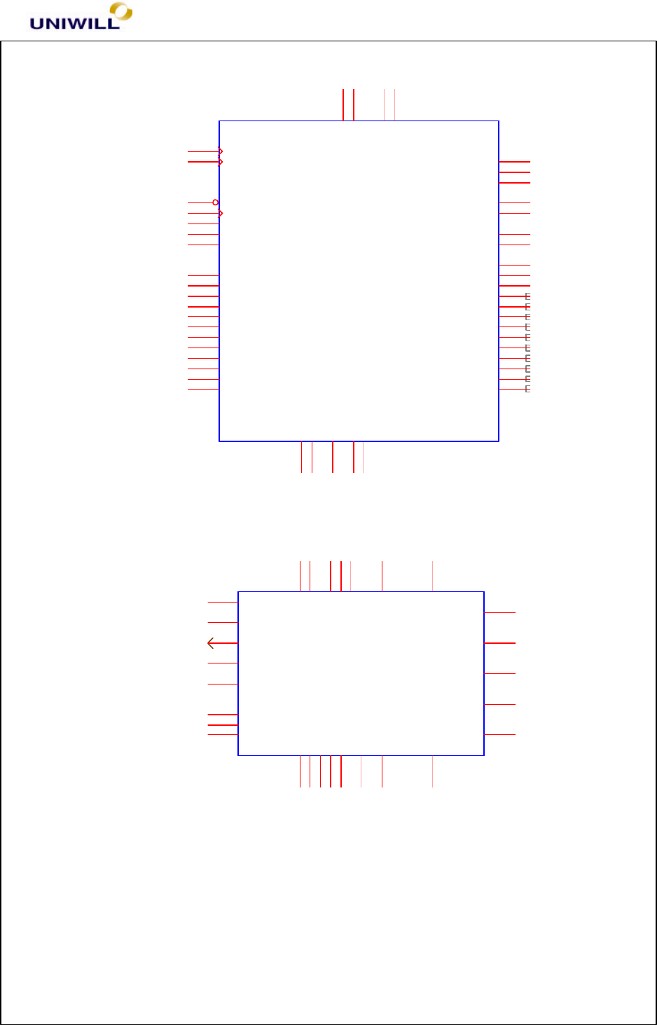
3.2 Major Components Pin Assignment
Chapter 5 Troubleshooting Guidelines
340S8 Rev : A Page
24
SOCKET_370 (U24A)
SOCKET_370 (U24B)
U24A
SOCKET_370
BCLK
W37
DEFER#
AN19
TRDY#
AN25
RESET#/RESET2#
X4
BPRI#
AN17
RS#[2]
AK28
RS#[1]
AH22
RS#[0]
AH26
VREF5 AD6
VREF3 R6
ADS#
AN31
HITM#
AL23
HIT#
AL25
DRDY#
AN27
DBSY#
AL27
LOCK#
AK20
BNR#
AH14
BREQ0#
AN29
REQ#[4]
AL17
REQ#[3]
AL19
REQ#[2]
AH18
REQ#[1]
AH16
REQ#[0]
AK18
A#[31]
AD4
A#[30]
AA3
A#[29]
Z4
A#[28]
AK6
A#[27]
AA1
A#[26]
Y3
A#[25]
AF6
A#[24]
AB4
A#[23]
AB6
A#[22]
AE3
A#[21]
AJ1
A#[20]
AC3
A#[19]
AG3
A#[18]
Z6
A#[17]
AE1
A#[16]
AN7
A#[15]
AL5
A#[14]
AK14
A#[13]
AL7
A#[12]
AN5
A#[11]
AK10
A#[10]
AH6
A#[9]
AL9
A#[8]
AH10
A#[7]
AL15
A#[6]
AN9
A#[5]
AH8
A#[4]
AH12
A#[3]
AK8
D#62
E25 D#63
F16
D#61
A27
D#60
A25
D#59
C17
D#58
C23
D#57
A19
D#56
C27
D#55
C19
D#54
C21
D#53
A23
D#52
D16
D#51
A13
D#50
C25
D#49
C13
D#48
A17
D#47
A15
D#46
A21
D#45
C11
D#44
A11
D#43
A7
D#42
D12
D#41
D14
D#40
C15
D#39
D10
D#38
D8
D#37
A9
D#36
C9
D#35
B2
D#34
C7
D#33
C1
D#32
F6
D#31
C5
D#30
J3
D#29
A3
D#28
A5
D#27
F12
D#26
E1
D#25
E3
D#24
K6
D#23
G3
D#22
F8
D#21
G1
D#20
L3
D#19
H6
D#18
P4
D#17
R4
D#16
H4
D#15
U3
D#14
N3
D#13
L1
D#12
Q1
D#11
M4
D#10
Q3
D#9
P6
D#8
S1
D#7
J1
D#6
T6
D#5
S3
D#4
U1
D#3
M6
D#2
N1
D#1
T4
D#0
W1
RESERVED/A#[33]
AC1
RESERVED/RSP# AC37
RESERVED/A#[35]
AF4
RESERVED/VTT AK16
RESERVED/AERR# AK24
RESERVED AK30
RESERVED/AP0# AL11
RESERVED/VTT AL13
RESERVED/VTT AL21
RESERVED/VTT AN11
RESERVED/AP1# AN13
RESERVED/VTT AN15
RESERVED/VTT AN21
RESERVED/RP# AN23
RESERVED/BINIT# B36
RESERVED/DEP5# C29
RESERVED/DEP1# C31
RESERVED/DEP0# C33
RESERVED/VTT E23
RESERVED/DEP6# E29
RESERVED/DEP4# E31
RESERVED F10
RESERVED/VTT G35
RESERVED G37
RESERVED L33
RESERVED N33
RESERVED N35
RESERVED N37
RESERVED Q33
RESERVED Q35
RESERVED Q37
RESERVED/VTT S33
RESERVED/VTT S37
RESERVED/VTT U35
RESERVED/VTT U37
RESERVED/BERR# V4
RESERVED/A#[34]
W3
TESTHI W35
RESERVED/A#[32]
X6
RESERVED Y1
VCORE-DET E21
RESERVED E27
RESERVED R2
RESERVED S35
RESERVED X2
PICCLK J33
PICD[0] J35
PICD[1] L35
PRDY# A35
PREQ# J37
PWRGOOD AK26
SLP# AH30
SMI# AJ35
TCK AL33
BPM#[1] E35
BSEL# AJ33
FLUSH# AE37
IERR# AE35
IGNNE# AG37
TRST# AN33
VREF4 V6
VREF1 F18
VREF0 E33
VREF7 AK22
VREF2 K4
VREF6 AK12
LINT[1]/NMI L37
INIT# AG33
BPM#[0] C35
BP#[3] E37
BP#[2] G33
FERR# AC35
A20M# AE33
CPUPRES#
C37
EDGCTRL/VRSEL AG1
PLL1 W33
PLL2 U33
THERMDP
AL31
THERMDN
AL29
LINT[0]/INTR M36
TDI AN35
TDO AN37
TMS AK32
VID[0] AL35
VID[1] AM36
VID[2] AL37
VID[3] AJ37
STPCLK# AG35
THERMTRIP#
AH28
RESERVED/VTT AH20
RESERVED/RESET#
AH4
RESERVED/DEP7# A29
RESERVED/DEP3# A31
RESERVED/DEP2# A33
RESERVED/VTT AA33
RESERVED/VTT AA35
VCC_1.5V AD36
VCC_2.5V Z36
VCC_CMOS AB36
GND/RESERVED AM2
BSEL1/GND AJ31
GND/CLKREF
Y33
Chapter 5 Troubleshooting Guidelines
340S8 Rev : A Page
25
Temperature Sensor (U5)
U24B
SOCKET_370
GND A37
GND AB32
GND AC33
GND AC5
GND
AD2
GND AD34
GND
AF32
GND AF36
GND
AG5
GND AH2
GND
AH34
GND AJ11
GND
AJ15
GND AJ19
GND
AJ23
GND AJ27
GND
AJ3
GND AJ7
GND
AK36
GND AK4
GND AL1
GND AL3
GND AM10
GND AM14
GND
AM18
GND
AM22
GND AM26
GND AM30
GND AM34
GND AM6
GND AN3
GND
B12
GND B16
GND
B20
GND B24
GND B28
GND B32
GND B4
GND B8
GND D18
GND D2
GND D22
GND D26
GND D30
GND D34
GND D4
GND E11
GND E15
GND E19
GND E7
GND F20
GND F24
GND F28
GND F32
GND F36
GND G5
GND H2
GND H34
GND K36
GND L5
GND M2
GND M34
GND P32
GND P36
GND Q5
GND R34
GND T32
GND T36
GND U5
GND V2
GND Z34
GND Z2
GND Y5
GND Y37
GND X36
GND X32
GND V34
VCC_CORE
AA37
VCC_CORE
AA5
VCC_CORE
AB2
VCC_CORE
AB34
VCC_CORE
AD32
VCC_CORE
AE5
VCC_CORE
AF2
VCC_CORE
AF34
VCC_CORE
AH24
VCC_CORE
AH32
VCC_CORE
AH36
VCC_CORE
AJ13
VCC_CORE
AJ17
VCC_CORE
AJ21
VCC_CORE
AJ25
VCC_CORE
AJ29
VCC_CORE
AJ5
VCC_CORE
AJ9
VCC_CORE
AK2
VCC_CORE
AK34
VCC_CORE
AM12
VCC_CORE
AM16
VCC_CORE
AM20
VCC_CORE
AM24
VCC_CORE
AM28
VCC_CORE
AM32
VCC_CORE
AM4
VCC_CORE
AM8
VCC_CORE
B10
VCC_CORE
B14
VCC_CORE
B18
VCC_CORE
B22
VCC_CORE
B26
VCC_CORE
B30
VCC_CORE
B34
VCC_CORE
B6
VCC_CORE
C3
VCC_CORE
D20
VCC_CORE
D24
VCC_CORE
D28
VCC_CORE
D32
VCC_CORE
D36
VCC_CORE
D6
VCC_CORE
E13
VCC_CORE
E17
VCC_CORE
E5
VCC_CORE
E9
VCC_CORE
F14
VCC_CORE
F2
VCC_CORE
F22
VCC_CORE
F26
VCC_CORE
F30
VCC_CORE
F34
VCC_CORE
F4
VCC_CORE
H32
VCC_CORE
H36
VCC_CORE
J5
VCC_CORE
K2
VCC_CORE
K32
VCC_CORE
K34
VCC_CORE
M32
VCC_CORE
N5
VCC_CORE
P2
VCC_CORE
P34
VCC_CORE
R32
VCC_CORE
R36
VCC_CORE
S5
VCC_CORE
T2
VCC_CORE
T34
VCC_CORE
V32
VCC_CORE
V36
VCC_CORE
W5
VCC_CORE
X34
VCC_CORE
Y35
VCC_CORE
Z32
Chapter 5 Troubleshooting Guidelines
340S8 Rev : A Page
26
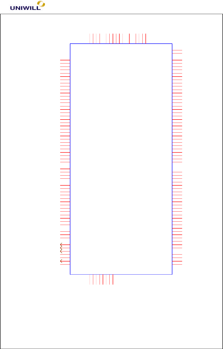
SIS-630S HOST and DRAM Interface (U10A)
SIS-630S PCI - IDE (U10B)
U5
ADM1021
NC
1
VCC
2
DXP
3
DXN
4
NC
5
ADD1
6
GND
7
GND
8NC 9
ADD0 10
ALERT# 11
SMBDATA 12
NC 13
SMBCLK 14
STBY# 15
NC 16
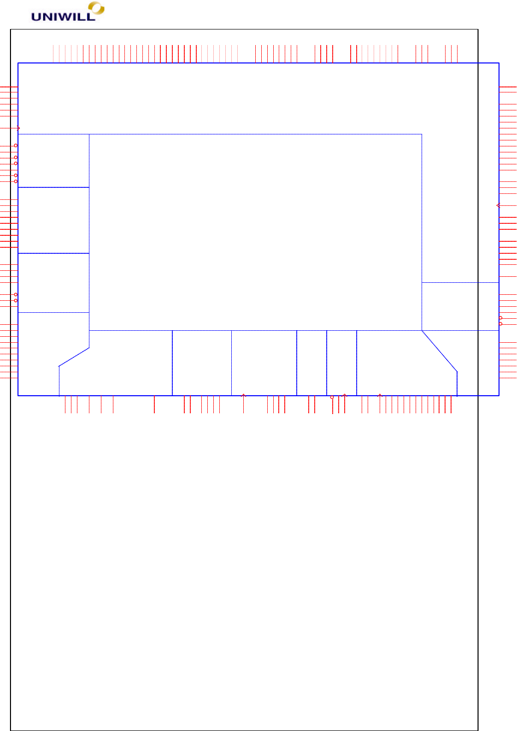
SIS-630S
DRAM CONTROLLER INTERFACE
HOST BUS INTERFACE
U10A
SIS-630S
CPUCLK
V29
DEFER#
R26
HTRDY#
P25
CPURST#
G27
BPRI#
R29
RS#[2]
V26
RS#[1]
R25
RS#[0]
U29
GTLREFB
A24
ADS#
U26
HITM#
R24
HIT#
U28
DRDY#
T27
DBSY#
U27
HLOCK#
T29
BNR#
P28
BREQ0#
G28
HREQ#[4]
R27
HREQ#[3]
T26
HREQ#[2]
T28
HREQ#[1]
R28
HREQ#[0]
P27
HA#[31]
M24
HA#[30]
H26
HA#[29]
G29
HA#[28]
J26
HA#[27]
H29
HA#[26]
H27
HA#[25]
K27
HA#[24]
H28
HA#[23]
J29
HA#[22]
J27
HA#[21]
K26
HA#[20]
J28
HA#[19]
K28
HA#[18]
L26
HA#[17]
L27
HA#[16]
L28
HA#[15]
K29
HA#[14]
M25
HA#[13]
M26
HA#[12]
M27
HA#[11]
L29
HA#[10]
N25
HA#[9]
N28
HA#[8]
M28
HA#[7]
M29
HA#[6]
N29
HA#[5]
N26
HA#[4]
P24
HA#[3]
N27
MD63 T25
MD62 W28
MD61 W27
MD60 Y29
MD59 Y27
MD58 Y26
MD57 AA28
MD56 AA26
MD55 AB28
MD54 AB26
MD53 AC29
MD52 AC27
MD51 AC25
MD50 AD28
MD49 AD27
MD48 Y25
MD47 AG22
MD46 AJ22
MD45 AF21
MD44 AH21
MD43 AF20
MD42 AH20
MD41 AJ20
MD40 AG19
MD39 AJ19
MD38 AF18
MD37 AH18
MD36 AF17
MD35 AG17
MD34 AJ17
MD33 AF16
MD32 AH16
MD31 T24
MA[13] AF27
MA[12] AF26
MA[11] AG29
MA[10] AG28
MA[9] AG27
MA[8] AH28
MA[7] AB24
MA[6] AH27
MA[5] AD24
MA[4] AJ27
MA[3] AG26
MA[2] AH26
MA[1] AJ26
MA[0] AF25
CSA#[2] AJ25
CSA#[1] AH25
CSA#[0] AG25
CSB#[3] AA25
CSB#[2] AE25
CSB#[1] AE26
DQM[7] Y24
DQM[6] AE28
DQM[5] AF23
DQM[4] AG23
DQM[3] AD25
DQM[2] AE29
DQM[1] AJ24
DQM[0] AD22
WE# AH23
SRAS# AH24
SCAS# AJ23
CKE E9
SDCLK AJ16
VSSQ
P26 VSSQ
B24
GTLREFA
P29
CPUAVDD
V27
MA[14] AB25
CSB#[0] AE27
CSA#[3] AF24
SDVADD
AE19
CSA#[4] AG24
CSA#[5] AE24
CSB#[4] AF29
CSB#[5] AF28
SDAVSS
AE20
CPUAVSS
V28
HD#0
G25 HD#1
G26 HD#2
F28 HD#3
F29 HD#4
K25 HD#5
L25 HD#6
F26 HD#7
E29 HD#8
F27 HD#9
F25 HD#10
K24 HD#11
H25 HD#12
E27 HD#13
D29 HD#14
E28 HD#15
J25 HD#16
D27 HD#17
E26 HD#18
C29 HD#19
H24 HD#20
D28 HD#21
C28 HD#22
F24 HD#23
B28 HD#24
C27 HD#25
B27 HD#26
D26 HD#27
A27 HD#28
A26 HD#29
C26 HD#30
E24 HD#31
B26 HD#32
E23 HD#33
D25 HD#34
F22 HD#35
E25 HD#36
C24 HD#37
B25 HD#38
C25 HD#39
D23 HD#40
D24 HD#41
D22 HD#42
E22 HD#43
A25 HD#44
C23 HD#45
B23 HD#46
C21 HD#47
A23 HD#48
D21 HD#49
A22 HD#50
C20 HD#51
C22 HD#52
B22 HD#53
D20 HD#54
E20 HD#55
D19 HD#56
A20 HD#57
A21 HD#58
B19 HD#59
B21 HD#60
B20 HD#61
C19 HD#62
A19 HD#63
E21
MD0 AG16
MD1 AE21
MD2 AH17
MD3 AD20
MD4 AJ18
MD5 AG18
MD6 AE18
MD7 AH19
MD8 AF19
MD9 AE22
MD10 AG20
MD11 AJ21
MD12 AG21
MD13 AE23
MD14 AH22
MD15 AF22
MD16 AD26
MD17 W25
MD18 AD29
MD19 AC26
MD20 AC28
MD21 V24
MD22 AB27
MD23 AB29
MD24 AA27
MD25 AA29
MD26 V25
MD27 Y28
MD28 W26
MD29 U25
MD30 W29
Chapter 5 Troubleshooting Guidelines
340S8 Rev : A Page
27
SIS-630S Power (U10C)
SIS-630S
PCI
IDE
U10B
SIS-630S
PREQ#[2]
C1
PREQ#[1]
C2
PREQ#[0]
C3
PCIRST#
C11
C/BE#[3]
F3
C/BE#[2]
H4
C/BE#[1]
J1
C/BE#[0]
L1
PAR
M6
FRAME#
H3
IRDY#
H2
TRDY#
H1
STOP#
J2
DEVSEL#
J3
PLOCK#
L4
ICHRDYA AE13
ICHRDYB AH13
IDREQ[A] AG8
IDREQ[B] AD17
IIRQA AF9
IIRQB AF15
PGNT#[2]
D2
PGNT#[1]
D3
PGNT#[0]
D4
IDECSA#[1] AF10
IDECSA#[0] AJ9
IIOR#[A] AH8
IIOR#[B] AG13
IIOW#[A] AF8
IIOW#[B] AF13
IDACK#[A] AJ8
IDACK#[B] AJ13
IDSAA[2] AD14
IDSAA[1] AE14
IDSAA[0] AG9
IDA14
AJ7 IDA13
AH7 IDA12
AF7 IDA11
AH6 IDA10
AG6 IDA9
AE6 IDA8
AJ5 IDA7
AH5 IDA6
AE11 IDA5
AF6 IDA4
AD12 IDA3
AJ6 IDA2
AG7 IDA1
AE12 IDA0
AE8
IDB15
AJ12
AD7 M4
AD4 M2
AD5 M3
AD6 N5
AD10 L3
AD11 K1
AD12 K2
AD13 M5
AD14 K3
AD15 K4
AD16 L5
AD17 G1
AD18 G2
AD19 G3
AD20 G4
AD21 F1
AD22 K5
AD23 F2
AD24 F4
AD25 E1
AD26 E2
AD27 K6
AD28 E3
AD29 J4
AD30 E4
AD31 D1
AD9 N6
AD8 L2
IDB0
AE17
IDB1
AG12
IDB2
AF12
IDB3
AH11
IDB4
AE16
IDB5
AJ10
IDB6
AD15
IDB7
AE15
IDB8
AG10
IDB9
AH10
IDB10
AF11
IDB11
AG11
IDB12
AJ11
IDB13
AD16
IDB14
AH12
IDA15
AD13
IDSAB[2] AG14
IDSAB[1] AF14
IDSAB[0] AD18
IDECSB#[1] AJ14
IDECSB#[0] AH14
CBLIDA AH9
CBLIDB AG15
AD3 M1
AD2 N4
AD1 P6
AD0 N3
PCICLK
AJ15
SERR#
B11
IDEAVDD
AH15
INTA#
N1
INTB#
P4
INTC#
P5
INTD#
P3
Chapter 5 Troubleshooting Guidelines
340S8 Rev : A Page
28
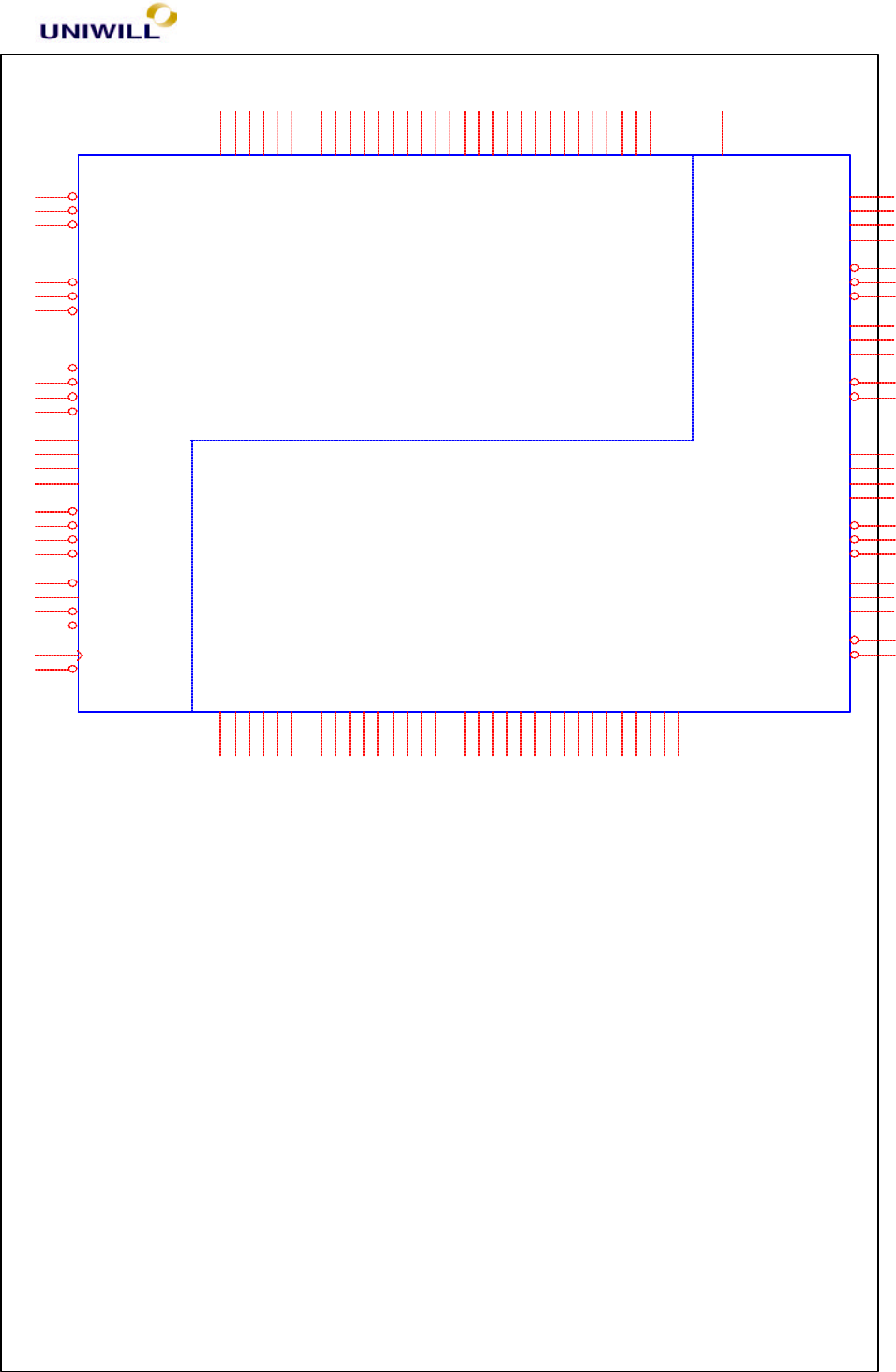
SIS 630S – VGA & South Bridge (U10D)
SIS-630S
POWER
U10C
SIS-630S
IVDD L21
IVDD U9
IVDD J10
IVDD J20
IVDD K21
IVDD J17
IVDD J16
IVDD J19
IVDD N21
IVDD L9
IVDD M21
IVDD N9
IVDD T21
IVDD J13
IVDD H16
OVDD
AA11
OVDD
AA12
OVDD
AA13
OVDD
AA18
OVDD
AA19
OVDD
AA20
OVDD
AA22
OVDD
AB12
OVDD
AB19
OVDD
AB21
OVDD
AB22
OVDD
H10
OVDD
H17
OVDD
J11
OVDD
J12
OVDD
J9
OVDD
K8
OVDD
K9
OVDD
M9
OVDD
U21
OVDD
U22
OVDD
V21
OVDD
V22
OVDD
W21
OVDD
W22
OVDD
Y21
PVDD H18
PVDD H12
PVDD H11
PVDD AB11
PVDD AB13
PVDD AB18
PVDD L8
PVDD AB20
PVDD M8
PVDD N22
PVDD J18
PVDD T22
PVDD Y22
VSSQ
V13
VSSQ
V12
VSSQ
U13
VSSQ
U12
VSSQ
U11
VSSQ
T13
VSSQ
T12
VSSQ
T11
VSSQ
R13
VSSQ
R12
VSSQ
R11
VSSQ
P13
VSSQ
P12
VSSQ
P11
VDDQ AA8
VDDQ AB8
VDDQ AA9
VDDQ AB9
VDDQ N8
VDDQ P8
VDDQ P9
VDDQ U8
VDDQ V8
VDDQ V9
VDDQ W8
VDDQ W9
VDDQ Y8
VDDQ Y9
GTLVTT H19
GTLVTT H20
GTLVTT H21
GTLVTT H22
GTLVTT J21
GTLVTT J22
GTLVTT K22
GTLVTT L22
GTLVTT M22
PVDD AB10
VSSD P16
VSSD P17
VSSD R16
VSSD R17
VSSD R18
VSSD R19
VSSD T16
VSSD T17
VSSD T18
VSSD T19
VSSD U16
VSSD U17
VSSD U18
VSSD U19
VSSD V16
VSSD V17
VSSD V18
VSSD W16
VSSD W17
IVDD H13
IVDD AB17
IVDD AB14
IVDD AA21
IVDD AA17
IVDD AA14
IVDD AA10
VSS
W15
VSS
W14
VSS
W13
VSS
V15
VSS
V14
VSS
U15
VSS
U14
VSS
T15
VSS
T14
VSS
R15
VSS
R14
VSS
P19
VSS
P18
VSS
P14 VSS
P15
VSS
N19
VSS
N18
VSS
L13 VSS
L14 VSS
L15 VSS
L16 VSS
L17 VSS
M12 VSS
M13 VSS
M14 VSS
M15 VSS
M16 VSS
M17 VSS
M18 VSS
N11 VSS
N12 VSS
N13 VSS
N14 VSS
N15 VSS
N16 VSS
N17
AUX1.8V
J8
AUX3.3V
H9
Chapter 5 Troubleshooting Guidelines
340S8 Rev : A Page
29
Clock Generator ( U18)
SIS-630S
VGA
ACPI
HOST
LPC
GPIO RTC OTHER MII SMB USB AC97
KBC
U10D
SIS-630S
DDC1DATA C15
DDC1CLK B16
RSET E19
VREF C14
VOSCI A11
HSYNC D15
VSYNC A16
BOUT A15
GOUT A14
ROUT B14
ECLKAVDD F15
DCLKAVDD F16
DACAVDDC F18
SSYNC C16
LAD1
AF4
LAD2
AJ4
LAD3
AE5
LDRQ#
AF5
LFRAME#
AH4
SIRQ
AG5
UV0+
J5 UV1-
G5 UV1+
H6 UV2-
E5 UV2+
F5
LAD0
AG4
UV3-
E6 UV3+
F6 UV4-
F8 UV4+
E7
PSON#
E11
ACPILED
C7
EXTSMI#
B12
PWRBTN#
E10
RING
B6
PME#
A6
THERM#
D13
KBDATA/GP10 B7
KBCLK/GP11 A7
PMDAT/GP12 D8
PMCLK/GP13 C8
KLOCK#/GP14/TXD B8
UV0-
H5
AC_SDIN[0] A10
AC_SDIN[1] B10
AC_SYNC B13
AC_RESET# D11
AC_SDOUT A13
GP7/SPDIF
E12
AC_BIT_CLK C13
SPK E18
SMCLK
AH3 SMBDATA
AG3 TXEN/GP15/SMBALT#
A8
ENTEST N2
GP6/CRS
C6 GP5/COL
F14 GP4/TXCLK
C10
GP2/LDRQ1#/TXD[2]
E17 GP1/PGNT3#/TXD[1]
D12 GP0/PREQ3#/TXD[0]
C12
RTCVDD
A4
RTCVSS
A3
OSC32KHI
B4
OSC32KHO
B5
AUXOK
A5 BATOK
C5
PWROK
C4
USBVDD1
B3
USBVDD0
B2
AAD0 AD6
AAD1 AG1
AAD2 AF3
AAD3 AF2
AAD4 AF1
AAD5 AE4
AAD6 AE3
AAD7 AE2
AAD8 AE1
AAD9 AD5
AAD10 AD4
AAD11 AD1
AAD12 AC4
AAD13 AC3
AAD14 AC2
AAD15 AC5
AAD16/B5 AA4
AAD17/B2 Y5
AAD18/B3 Y4
AAD19/B0 Y3
AAD20/B1 Y2
AAD21/R1 Y1
AAD22/R2 W4
AAD23/R3 W3
AAD24/R4 V5
AAD25/R5 V4
AAD26/R6 V3
AAD27/R7 V2
AAD28/G2 V1
AAD29/G0 U5
AAD30G1 U4
AAD31/G3 W5
SBA0/BBLANK# R3
SBA1/DDC2DAT R2
SBA2/DDC2CLK R1
SBA3/G7 T1
SBA4/G6 T4
SBA5/G5 T5
SBA6/G4 U1
SBA7 U2
AC/BE0# AG2
AC/BE1# AC1
B4/AC/BE2# AA3
R0/AC/BE3# U3
VBCAD/AREQ# R6
VGCLK/AGNT# T6
B6/AIRDY# Y6
B7/AFRAME# AB2
ATRDY# AB3
ADEVSEL# AB4
ASERR# AB6
APAR AA5
ASTOP# AB5
VBHCLK/RBF# P2
VBVSYNC/ST1 R5
VBHSYNC/ST0 V6
VBCLK/ST2 R4
VBCTL0/WBF# P1
VBCTL1/PIPE# U6
AGPVREF AA1
AGPRCOMP AB1
AGPAVDD1 AE10
AGPAVDD2 AE9
DACAVDDB E14
AGPAVSS1 AD10
AGPAVSS2 AD8
ECLKAVSS E15
DCLKAVSS E16
DACAVSSC F20
DACAVSSB D14
COMP B15
AGPVSSREF AA2
UV5-
E8 UV5+
D7 USBCLK48M
A12
RXDV/OC0#
F10 MDIO/OC1#
D6
RXD[0]
C9 RXD[1]
B9 RXD[2]
E13 RXD[3]
A9
LANCLK25M
D5
RESERVE1
AH2 RESERVE2
AE7
VSSA
F13
VSSB
F17
VSSC
N24
VSSD
U24
AD_STB1#
W2
AD_STB0#
AD3
AD_STB1
W1
AD_STB0
AD2
SB_STB#
T3
SB_STB
T2
AGPCLK
AJ3
NMI
C18
SMI#
D16
INTR
D18
A20M#
B17
INIT#
A17
IGNNE#
B18
FERR#
A18
STPCLK#
C17
CPUSTOP#/CPUSLP
D17
GP3/RXER
F12
GP8/MDC
D9
GP9/RXCLK
D10
Chapter 5 Troubleshooting Guidelines
340S8 Rev : A Page
30
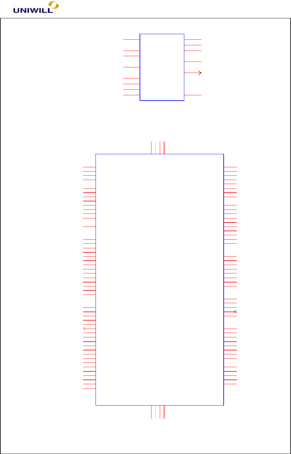
RAM Switch (U29)
RTL 8201 (U2) Octal Buffer (U25)
U18
W83194BR-63S
VDDREF
1
AGPSEL/REF1 2
FS3/REF0 3
GNDREF
4
X1
5
X2
6
VDDPCI
7
FS1/PCICLK_F 8
FS2/PCICLK1 9
PCICLK2 10
PCICLK3 11
PCICLK4 12
PCICLK5 13
GNDPCI
14
VDDAGP
15
AGPCLK0 16
AGPCLK1 17
GNDAGP
18 GND48
19
FS0/48MHZ 20
MODE/24_48MHZ 21
VDD48
22
SDATA
23 SCLK
24
VDDSDR
25
SDRAM12 26
CPUSTP#/SDRAM11 27
PCISTP#/SDRAM10 28
GNDSDR
29
SDRSTOP#/SDRAM9 30
PD#/SDRAM8 31
GNDSDR
32
SDRAM7 33
SDRAM6 34
VDDSDR
35
SDRAM5 36
SDRAM4 37
SDRAM3 38
GNDSDR
39
SDRAM2 40
SDRAM1 41
SDRAM0 42
VDDSDR
43
GNDCPU
44
CPUCS_C2 45
CPU_C1 46
CPU_C0 47
VDDCPU
48
+3V +3V
+5V
+3V
SDRAMSEL17
I2CSDA1,5,6
I2CSCL1,5,6
0 ohm
10K
74HCT4066
TSSOP-14P
10K 10K
DTC144EKA
RAM_I2CSDA
RAM_I2CSCL
RAM_I2CSDA
RAM_I2CSCL
B_I2CSDA
A_I2CSCL
A_I2CSDA
B_I2CSCL
R353
10K
R352
10K
U29 74HCT4066
1Y
1
2Y
4
3Y
8
4Y
11 4Z 10
3Z 9
2Z 3
1Z 2
1E
13
2E
5
3E
6
4E
12
VCC 14
GND
7
Q47
DTC144EKA
B
CE
RP44
8P4RX10K
1
2
3
4 5
6
7
8
R368 0
R369 R
Chapter 5 Troubleshooting Guidelines
340S8 Rev : A Page
31
LVDS Transmitter (U8)
Audio CODEC (U1)
U8
DS90CF363A
D0/R0
44
D1/R1
45
D2/R2
47
D3/R3
48
D4/R4
1
D5/R5
3
D6/G0
4
D7/G1
6
D8/G2
7
D9/G3
9
D10/G4
10
D11/G5
12
D12/B0
13
D13/B1
15
D14/B2
16
D15/B3
18
D16/B4
19
D17/B5
20
D18/HSYNC
22
D19/VSYNC
23
D20/ENABLE
25
CLKIN
26
VCC 2
VCC 8
VCC 21
GND 5
GND 11
GND 17
GND 24
GND 46
PLLVCC 29
LVDSVCC 37
LVDSGND 42
PLLGND 30
LVDSGND 31
LVDSGND 36
Y0- 41
Y0+ 40
Y1- 39
Y1+ 38
Y2+ 34
Y2- 35
SHUTN#
27
NC
14
NC
43
CLKOUT+ 32
CLKOUT- 33
PLLGND 28
U2
RTL8201
TXEN
2
TXC
7
TXD0
6
TXD1
5
TXD2
4
TXD3
3
MDC
25
MDIO
26
RXDV
22
RXD0
21
RXD1
20
RXD2
19
RXD3
18
RXC
16
COL
1
CRS
23
RXER
24
X1
46
X2
47 LED0/PHYA0 9
LED1/PHYA1 10
LED2/PHYA2 12
LED3/PHYA3 13
LED4/PHYA4 15
DVDD 8
DVDD 14
AVDD0 32
AVDD1 36
PLLVDD 48
DGND
11
DGND
17
AGND
29
AGND
35
AGND
45
RESETB
42
TPRX+ 31
TPRX- 30
TPTX- 33
TPTX+ 34
RTT3 27
MII/SNIB 44
LDPS 41
ANE 37
DUPLEX 38
SPEED 39
REPT 40
ISOLATE 43
RTSET 28
U25
74LVC244
OE1#
1
I-0
2
I-1
4
I-2
6
I-3
8
I-4
17
I-5
15
I-6
13
I-7
11
OE2#
19
VCC 20
O-0 18
O-1 16
O-2 14
O-3 12
GND 10
O-4 3
O-5 5
O-6 7
O-7 9
Chapter 5 Troubleshooting Guidelines
340S8 Rev : A Page
32
Audio Amplifier (U4)
PCMCIA Controller (U22)
U1
AVANCE_ALC200_SQFP-48
VDD 1
VDD 9
AVDD 25
AVDD 38
GND
4
GND
7
AGND
26
AGND
42
XTL-IN
2
XTL-OUT
3
SDOUT
5
BITCLK
6
SDIN
8
SYNC
10
RESET#
11
PC-BEEP
12
PHONE
13
AUX-L
14
AUX-R
15
VIDEO-L
16
VIDEO-R
17
CD-L
18
CD-R
20
CD-GND
19
MIC1
21
MIC2
22
LINE-L
23
LINE-R
24
VREF 27
VREFOUT 28
AFILT1 29
AFILT2 30
AFILT3/CAP1 31
CAP2 32
M-VREF/CAP3 33
M-AFILT/CAP4 34
LINEOUT-L 35
LINEOUT-R 36
MONO-OUT 37
HPOUT-L/CAP11 39
HPOUT-C/CAP12 40
HPOUT-R/CAP13 41
HXAN/CAP5 43
HXAP/CAP6 44
TXAN/CAP7 45
TXAP/CAP8 46
RXAN/CAP9 47
RXAP/CAP10 48
U4
LM4835
R_IN
10
R_DOCK
9
B_IN
11
L_DOCK
13
L_IN
12
SHUTDOWN
2
MUTE
5
MODE
4
R_OUT- 26
R_OUT+ 28
L_OUT+ 15
L_OUT- 17
HP_SENSE 21
G_SEL 3
DC_VOL 7
VDD 6
VDD 16
VDD 27
R_GAIN1 24
R_GAIN2 25
L_GAIN2
18
L_GAIN1
19
BYPASS
22
GND
1
GND
8
GND
14
GND
20
GND
23
Chapter 5 Troubleshooting Guidelines
340S8 Rev : A Page
33
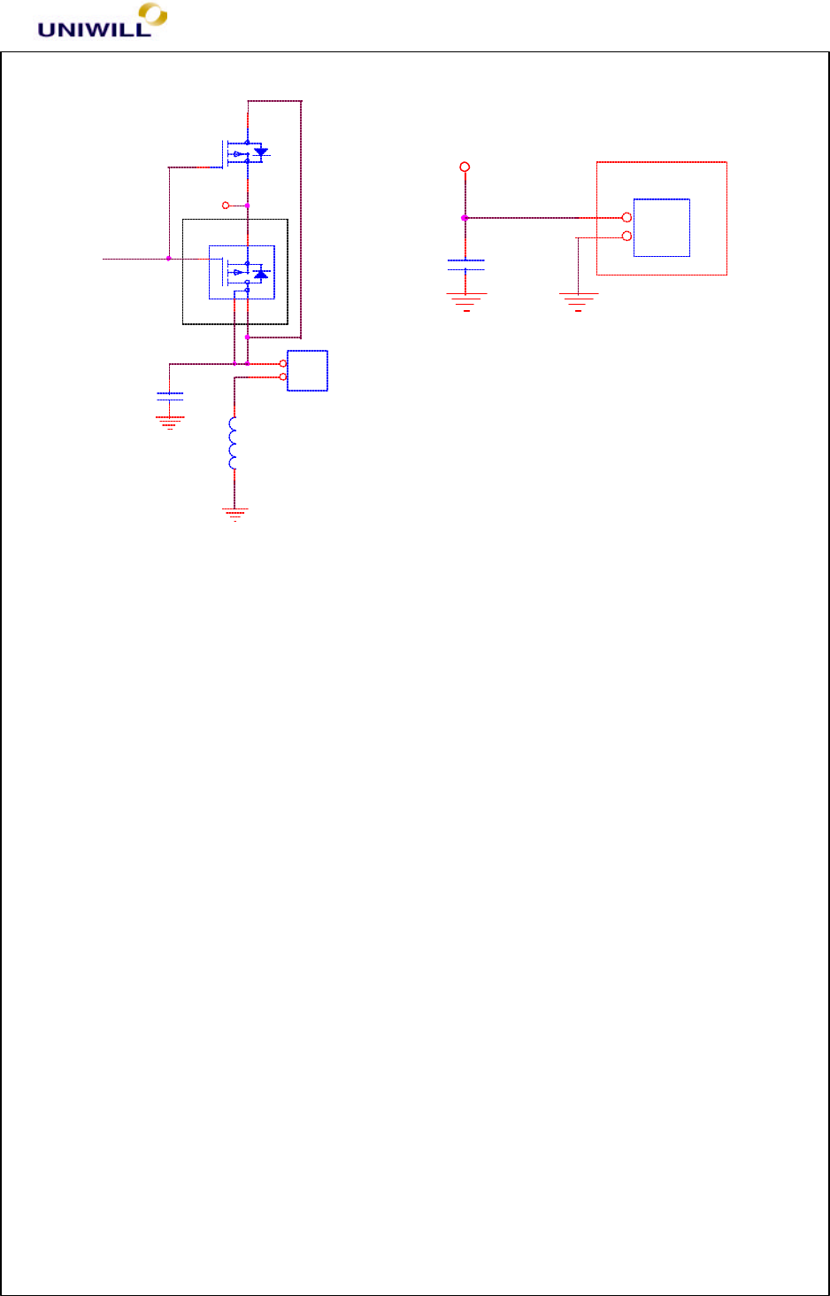
PCMCIA Power Controller (U21)
U22
OZ6812TQFP
PCI_VCC 18
PCI_VCC 30
PCI_VCC 44
PCI_VCC 50
CORE_VCC 14
CORE_VCC 66
CORE_VCC 86
CORE_VCC 102
CORE_VCC 122
CORE_VCC 138
AUX_VCC 63
VCCD0#/VCC5#/SDAT 73
VCCD1#/VCC3#/SCLK 74
VPPD0/VPP_PGM/SLAT 71
VPPD1/VPP_VCC 72
SKT_VCC 90
SKT_VCC 126
CAD31 144
CAD30 142
CAD29 141
CAD28 140
CAD27 139
CAD26 129
CAD25 128
CAD24 127
CAD23 124
CAD22 121
CAD21 120
CAD20 118
CAD19 116
CAD18 115
CAD17 113
CAD16 98
CAD15 96
CAD14 97
CAD13 93
CAD12 95
CAD11 92
CAD10 91
CAD9 89
CAD8 87
CAD7 85
CAD6 82
CAD5 83
CAD4 80
CAD3 81
CAD2 77
CAD1 79
CAD0 76
CCLK 108
CFRAME# 111
CIRDY# 110
CTRDY# 109
CDEVSEL# 107
CSTOP# 105
CPAR 101
CPERR# 104
CSERR# 133
CREQ# 123
CGNT# 106
CINT# 132
CBLOCK# 103
CCLKRUN# 136
CRST# 119
R2_D2 143
R2_D14 84
R2_A18 100
CVS1 131
CVS2 117
CCD1# 75
CCD2# 137
CAUDIO 134
CSTSCHG 135
CC/BE3# 125
CC/BE2# 112
CC/BE1# 99
CC/BE0# 88
AD31
3
AD30
4
AD29
5
AD28
7
AD27
8
AD26
9
AD25
10
AD24
11
AD23
15
AD22
16
AD21
17
AD20
19
AD19
23
AD18
24
AD17
25
AD16
26
AD15
38
AD14
39
AD13
40
AD12
41
AD11
43
AD10
45
AD9
46
AD8
47
AD7
49
AD6
51
AD5
52
AD4
53
AD3
54
AD2
55
AD1
56
AD0
57
C/BE3#
12
C/BE2#
27
C/BE1#
37
C/BE0#
48
IDSEL
13
PCI_CLK
21
DEVSEL#
32
FRAME#
28
IRDY#
29
TRDY#
31
STOP#
33
PAR
36
PERR#
34
SERR#
35
REQ#
1
GNT#
2
RST#
20
RI_OUT#/PME#
59
SUSPEND#
70
SPKR_OUT#
62
MF6
69
MF5
68
MF4
67
MF3
65
MF2
64
MF1
61
MF0
60
GND
6
GND
22
GND
42
GND
58
GND
78
GND
94
GND
114
GND
130
Chapter 5 Troubleshooting Guidelines
340S8 Rev : A Page
34
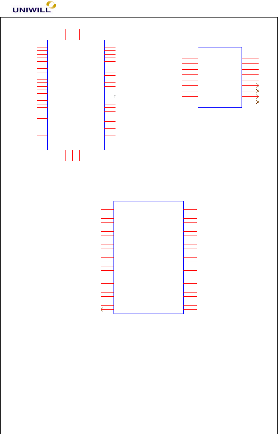
Super I/O Controller (U14)
Switch (U16) QSOP-28 (U35)
U21
MIC2562A
V5_EN
1
V3_EN
2
EN0
3
EN1
4
FLAG# 5
VPPIN
6VPPOUT 7
VCCOUT 8
V3IN
9
VCCOUT 10
V5IN
11 VCCOUT 12
V5IN
13
GND 14
PC87393
U14
PC87393
LAD0
15
LAD1
16
LAD2
17
LAD3
18
LCLK
8
LRESET#
9
LFRAME#
12
CLKRUN#/GPIO36
6LPCPD#
7LDRQ#
11
SERIRQ
10
SMI#/GPIO35
19
CLKIN
20
VDD 14
VDD 39
VDD 63
VDD 88
VSS
13
VSS
38
VSS
64
VSS
89
DSKCHG#
21
HDSEL#
22
RDATA#
23
WP#
24
TRK0#
25
WGATE#
26
WDATA#
27
SETP#
28
DIR#
29
DR0#
30
MTR0#
31
INDEX#
32
DENSEL
33
DRATE0/IRSL2
34
PD0/INDEX# 52
PD1/TRK0# 50
PD2/WP# 48
PD3/RDATA# 46
PD4/DSKCHG# 45
PD5/MSEN0 44
PD6/DRATE0 43
PD7/MSEN1 42
PNF/XRDY 35
SLCT/WGATE# 36
PE/WDATA# 37
BUSY_WAIT#/MTR1# 40
ACK#/DR1# 41
SLIN#_ASTRB#/STEP# 47
INIT#/DIR# 49
ERR#/HDSEL# 51
AFD#_DSTRB#/DENSEL 53
STB#_WRITE# 54
DCD1# 55
DSR1# 56
SIN1 57
RTS1#/TEST 58
SOUT1/XCNF0 59
CTS1# 60
DTR1#_BOUT1/BADDR 61
RI1# 62
IRTX 70
IRRX1 69
IRRX2_IRSL0 68
IRSL1 67
IRSL3/PWUREQ# 66
XD0/GPIO00/JOYABTN1 3
XD1/GPIO01/JOYBBTN1 2
XD2/GPIO02/JOYAY 1
XD3/GPIO03/JOYBY 100
XD4/GPIO04/JOYBX 99
XD5/GPIO05/JOYAX 98
XD6/GPIO06/JOYBBTN0 97
XD7/GPIO07/JOYABTN0 96
XWR#/XCNF1 4
XRD#/GPIO34/WDO# 5
XIOWR#/XCS1#/MTR1#/DRATE0 73
XIORD#/GPIO37/IRSL2/DR1# 71
XCS0#/DR1#/XDRY/GPIO25 72
XA19/DCD2#/JOYABTN0/GPIO17
74 XA18/GPIO16/JOYBBTN0/DSR2#
75 XA17/GPIO15/JOYAX/SIN2
76 XA16/GPIO14/JOYBX/RTS2#
77 XA15/GPIO13/JOYBY/SOUT2
78 XA14/GPIO12/JOYAY/CTS2#
79 XA13/GPIO11/JOYBBTN1/DTR2#_BOUT2
80 XA12/GPIO10/JOYABTN1/RI2#
81 XA11/GPIO33/XIOWR#/MDTX
82 XA10/GPIO32/XIORD#/MDRX
83 XA9/GPIO31/MTR1#/PIRQD
84 XA8/GPIO30/PIRQC
85 XA7/GPIO27/PIRQB
86 XA6/GPIO26/PRIQA/XSTB2#
87 XA5/XSTB1#/XCNF2
90 XA4/GPIO24/XSTB0#
91 XA3/GPIO23
92 XA2/GPIO22
93 XA1/GPIO21
94 XA0/GPIO20
95
Chapter 5 Troubleshooting Guidelines
340S8 Rev : A Page
35
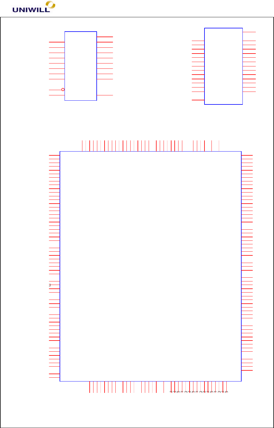
Keyboard Controller (PC87570)
RS-232 Transceiver (U3) BIOS EEPROM Socket (U17)
U35
1284-02
DIN0
3
DIN1
4
DIN2
5
DIN3
6
DIN4
7
DIN5
9
DIN6
11
DIN7
13
DIN8
14
DOUT0 26
DOUT1 25
DOUT2 24
DOUT3 23
DOUT4 21
DOUT7 17
DOUT8 16
DOUT5 19
DOUT6 18
NODE0
1
NODE1
2
NODE2
8
NODE3
10
GND
22
NODE7 28
NODE6 27
NODE5 15
NODE4 12
VCC 20
U16
74LVC373
D0
3
D1
4
D2
7
D3
8
D4
13
D5
14
D6
17
D7
18
OC
1
G
11
Q0 2
Q1 5
Q2 6
Q3 9
Q4 12
Q5 15
Q6 16
Q7 19
GND 10
VCC 20
U19
PC87570
32CLKIN/32KX1
25
32KX2
27
RING#/PB0
71
SCL/PB1
72
SDA/PB2
73
TA/PB3
74
EXINT10/TB/PB4
75
GA20/PB5
76
HRSTO#/PB6
77
SWIN/PB7
78
PC0 61
PC1 62
PC2 63
EXITN0/PC3 64
EXTIN11/PC4 65
EXTIN15/PC5 68
PSCLK3/PC6 70
PSDAT3/PC7 69
AD3/PD3 84
AD6/PD6 93
AD7/PD7 94
ENV0/BST0/PH0
104
ENV1/BST1/PH1
103
TRIS/BST2/PH2
102
PFS/PH3
101
PLI/PH4
100
ISE#/PH5
99
KBSN0
36
KBSN1
35
KBSN2
34
KBSN3
33
KBSN4
32
KBSN5
31
KBSN6
30
KBSN7
29
KBSOUT0
56
KBSOUT1
55
KBSOUT2
54
KBSOUT3
53
KBSOUT4
52
KBSOUT5
51
KBSOUT6
50
KBSOUT7
49
KBSOUT8
48
KBSOUT9
47
KBSOUT10
42
KBSOUT11
41
KBSOUT12
40
KBSOUT13
39
KBSOUT14
38
KBSOUT15
37
IRQ1
156
IRQ8#
155
IRQ11
154
IRQ12
153
PFAIL#
79
HPWRON
165
VBAT
28
GND
160 GND
109 GND
66 GND
26 GND
24
VCC 23
VCC 67
VCC 108
VCC 161
AVCC 91
AVREF 80
AGND
92
HA0 166
HA1 167
HA2 168
HA3 169
HA4 170
HA5 171
HA6 172
HA7 173
HA8 174
HA9 3
HA10 4
HA11 5
HA12 6
HA13 7
HA14 8
HA15 9
HA16/PA3 10
HA17/PA4 11
HA18/PE0 12
HD0 15
HD1 16
HD2 17
HD3 18
HD4 19
HD5 20
HD6 21
HD7 22
HMEMCS#/PA0
157 HEMERD#/PA1
162 HEMEWR#/PA2
163 HAEN
13 HIOR#
158 HIOW#
159 HIOCHRDY
14
A0 114
A1 115
A2 116
A3 117
A4 118
A5 119
A6 120
A7 121
A8 122
A9 123
A10 124
A11 125
A12 126
BE0/A13 127
BE1/A14 128
CBRD/PG1/A15 129
PA5/A16 130
D0 137
D1 138
D2 139
D3 140
D4 141
D5 142
D6 143
RD#/HDEN 111
SEL0#/HRMS 105
WR0# 112
SELIO#/PG0 110
CLK/PG2 107
SEL1#/PG3 106
WR1/PG4 113
PF0/D8
145
PF1/D9
146
PF2/D10
147
PF3/D11
148
PF4/D12
149
PF5/D13
150
PF6/D14
151
PF7/D15
152
HMR
164
PA6/A17 135
D7 144
SHBM#/PE1/A18 136
PSDAT1 57
PSCLK1 58
PSDAT2 59
PSCLK2 60
AD0/PD0 81
AD1/PD1 82
AD2/PD2 83
AD4/PD4 85
AD5/PD5 86
DA0
95
DA1
96
DA2
97
DA3
98
NC
89
NC
90
NC
131
NC
132
NC
133
NC
134
NC
175
NC
176
NC
88 NC
87 NC
46 NC
45 NC
44 NC
43 NC
2NC
1
Chapter 5 Troubleshooting Guidelines
340S8 Rev : A Page
36
PWM Control (U28) PWM Control (U34)
Low Dropout Regulator (U26) Linear Regulator (U32)
DC-DC Converter (U30) Charger (U33)
U17
29LV020 (PLCC-32)
A0
12
A1
11
A2
10
A3
9
A4
8
A5
7
A6
6
A7
5
A8
27
A9
26
A10
23
A11
25
A12
4
A13
28
A14
29
A15
3
A16
2CE 22
OE 24
A18
1
WE# 31
O0 13
O1 14
O2 15
O3 17
O4 18
O5 19
O6 20
O7 21
VCC 32
VSS 16
A17
30
U3
GD75232
ROUT1
19
ROUT2
18
ROUT3
17
ROUT4
14
ROUT5
12
DIN1
16
DIN2
15
DIN3
13
RIN1 2
RIN2 3
RIN3 4
RIN4 7
RIN5 9
DOUT1 5
DOUT2 6
DOUT3 8
VCC
20 V+ 1
V- 10
GND
11
U28
TL594-SOP16
1IN+
1
1IN-
2
FB
3
DTC 4
CT 5
RT 6
GND
7
C1 8
E1 9
E2
10
C211
VCC 12
OUT-CTRL
13
REF
14
2IN-
15 2IN+
16
U34
TL594-SOP16
1IN+
1
1IN-
2
FB
3
DTC 4
CT 5
RT 6
GND
7
C1 8
E1 9
E2
10
C211
VCC 12
OUT-CTRL
13
REF
14
2IN-
15 2IN+
16
U26
AME8800DEFT
GND
1
IN
3OUT2
U32
78L12-SO8
Vout 1
GND 2
GND 3
GND
6GND
7Vin
8
N.C
5N.C 4
Chapter 5 Troubleshooting Guidelines
340S8 Rev : A Page
37
LTC 1736 (U27)
U30
BA9743AFV-SOP16
CT 1
RT 2
1IN+ 3
1IN- 4
1FB 5
1DTC 6
1OUT 7
GND 8
VCC
9
2OUT
10
2DTC
11
2FB
12
2IN-
13
2IN+
14
SCP
15
REF
16
U33
MB3878
-INC2
1
OUTC2
2
+INE2
3
-INE2
4
FB2
5
VREF
6
FB1
7
-INE1
8
+INE1
9
OUTC1
10
OUTD
11
-INC1
12 +INC1
13
CTL
14
FB3
15
-INE3
16
RT
17
VCC
18
VH
19
OUT
20
VCC(O)
21
CS
22
GND
23
+INC2
24
SSOP 24
U27
LTC1736
Cosc
1
RUN/SS
2
Ith
3
FCB
4
SGND
5
PGOOD
6
SENSE-
7
SENSE+
8
VFB
9
Vosense
10
B0
11
B1
12 B2
13
B3
14
B4
15
VIDVcc
16
EXTVcc
17
PGND
18
BG
19
INTVcc
20
Vin
21
SW
22
BOOST
23
TG
24
Chapter 5 Troubleshooting Guidelines
340S8 Rev : A Page
38

Chapter 5 Troubleshooting Guidelines
340S8 Rev : A Page
39
Chapter 5 Troubleshooting Guidelines
340S8 Rev : A Page
40
System Disassembly Procedure
Chapter 5 Troubleshooting Guidelines
340S8 Rev : A Page
41
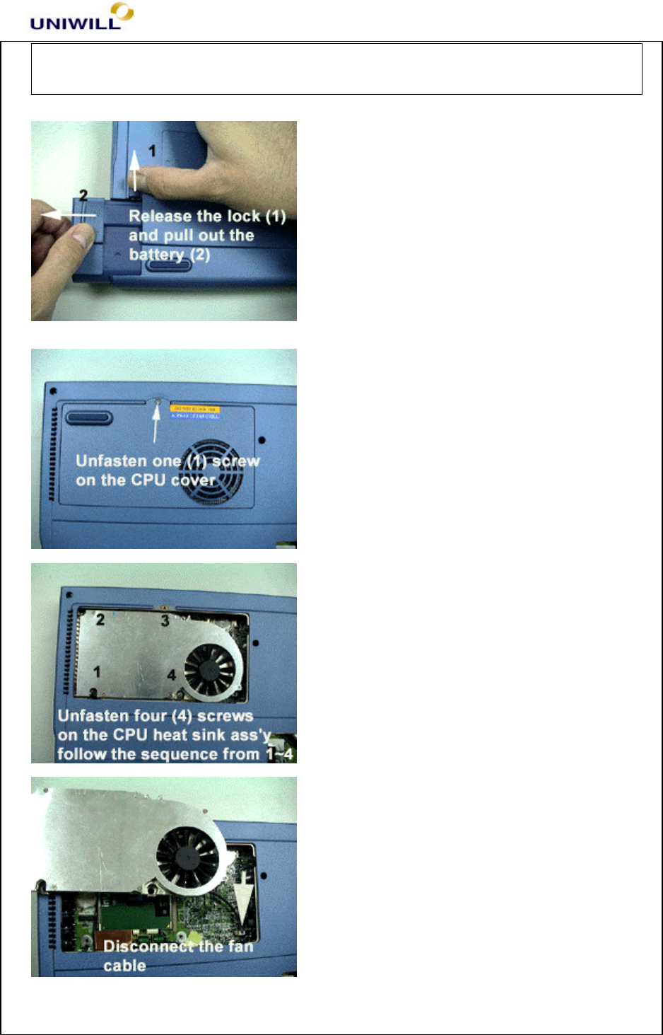
1. Before doing the disassembly, you MUST first remove the battery from the battery
compartment and no external power is supplied to the machine.
2. Unfasten the one (1) screw on the CPU cover.
3. Unfasten four (4) screws on the CPU fan + heat sink assembly. Please follow the sequence
when unfastening.
When fastening, you must start on # 4 , 3 , 2 and 1 ( counter clockwise direction)
4. Disconnect the cable CPU fan + heat sink assembly from the mainboard.
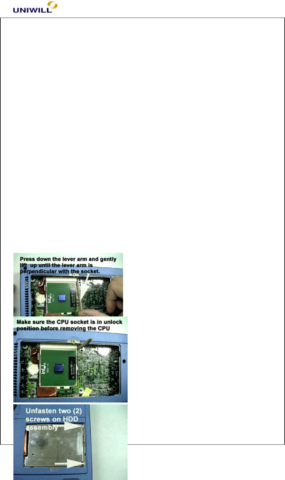
5. Gently press down the lever arm of the CPU
socket and lift it up until the lever arm is in
stand position.
Chapter 5 Troubleshooting Guidelines
340S8 Rev : A Page
42
6. Make sure the CPU socket is in release position before you remove the CPU.
7. Unfasten one (1) screw on the HDD cover.
8. Unfasten two (2) screws on the HDD metal bracket.
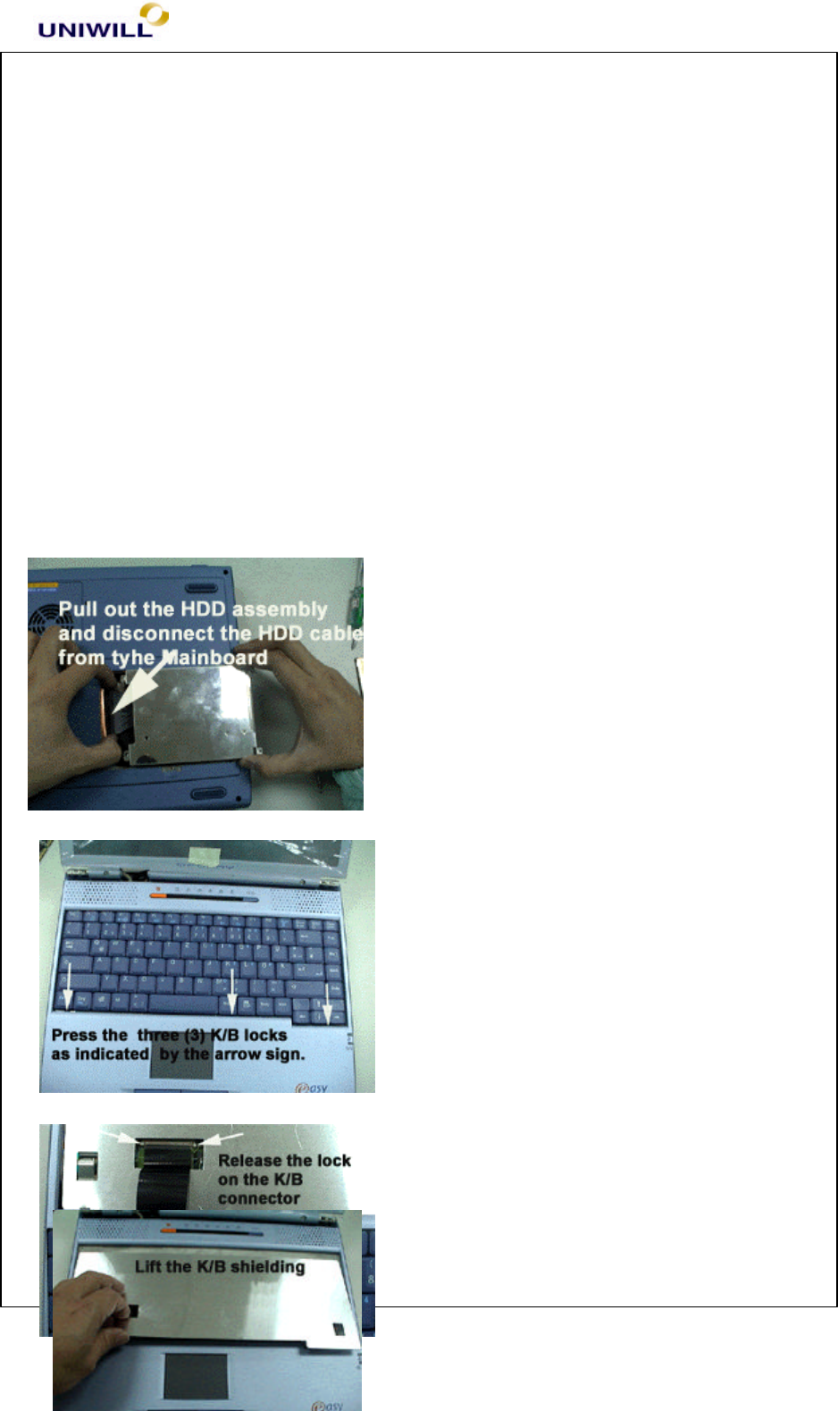
9. Pull out the HDD assembly and disconnect the
HDD cable from the mainboard.
Chapter 5 Troubleshooting Guidelines
340S8 Rev : A Page
43
10. Use a small flat screwdriver , insert to the K/B lock to release the three lock.
11. Gently lift the keyboard and disconnect the keyboard cable from the connector.
12. Remove the keyboard shielding or plate.
Chapter 5 Troubleshooting Guidelines
340S8 Rev : A Page
44
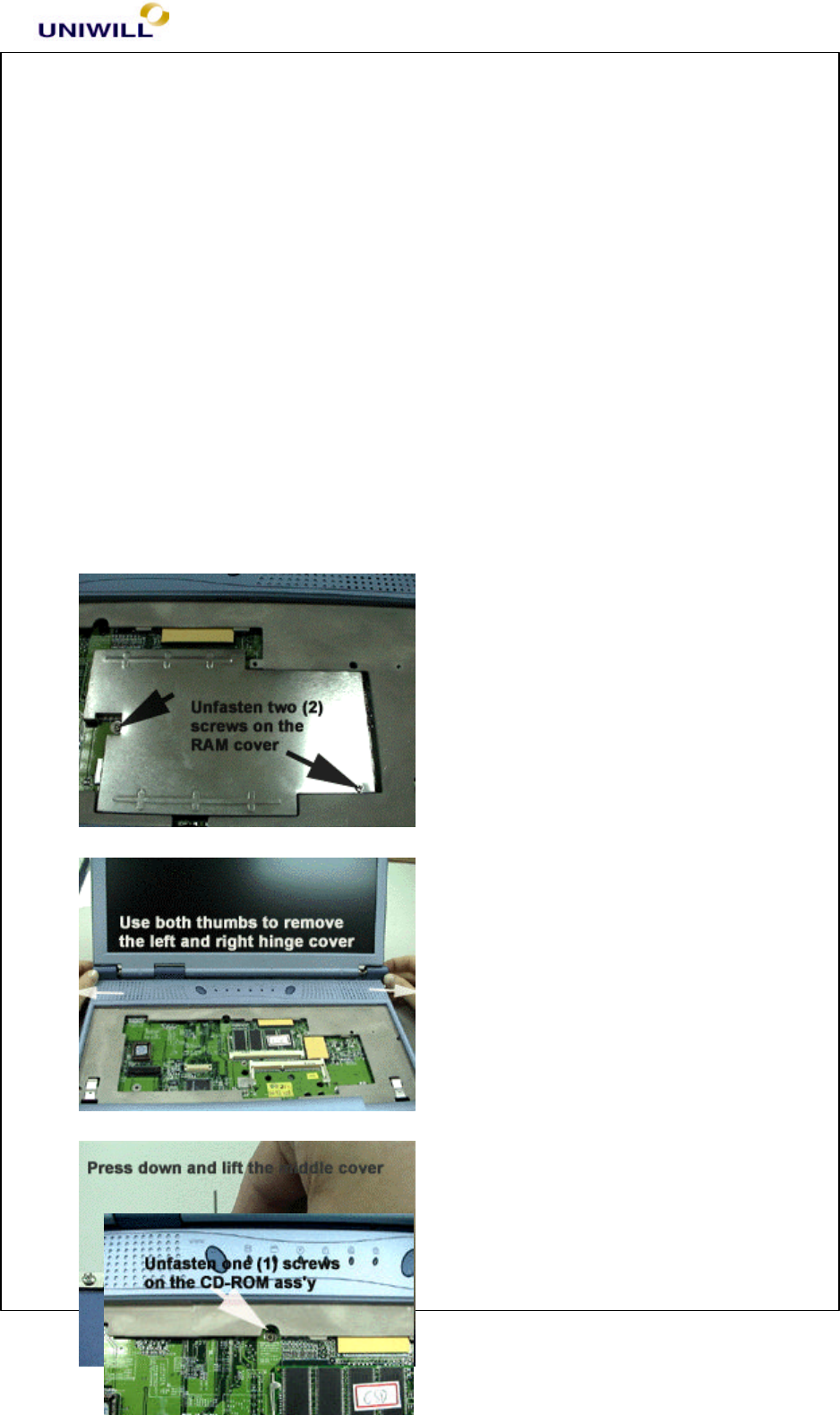
13. Unfasten two (2) screws on the ram cover and remove the RMA cover.
14. Use both thumbs, push in and remove the left and right hinge covers.
15. Close the display panel, press down the middle cover and then pull out to remove.
16. Unfasten one screws of the CD-ROM ( or DVD-ROM drive).
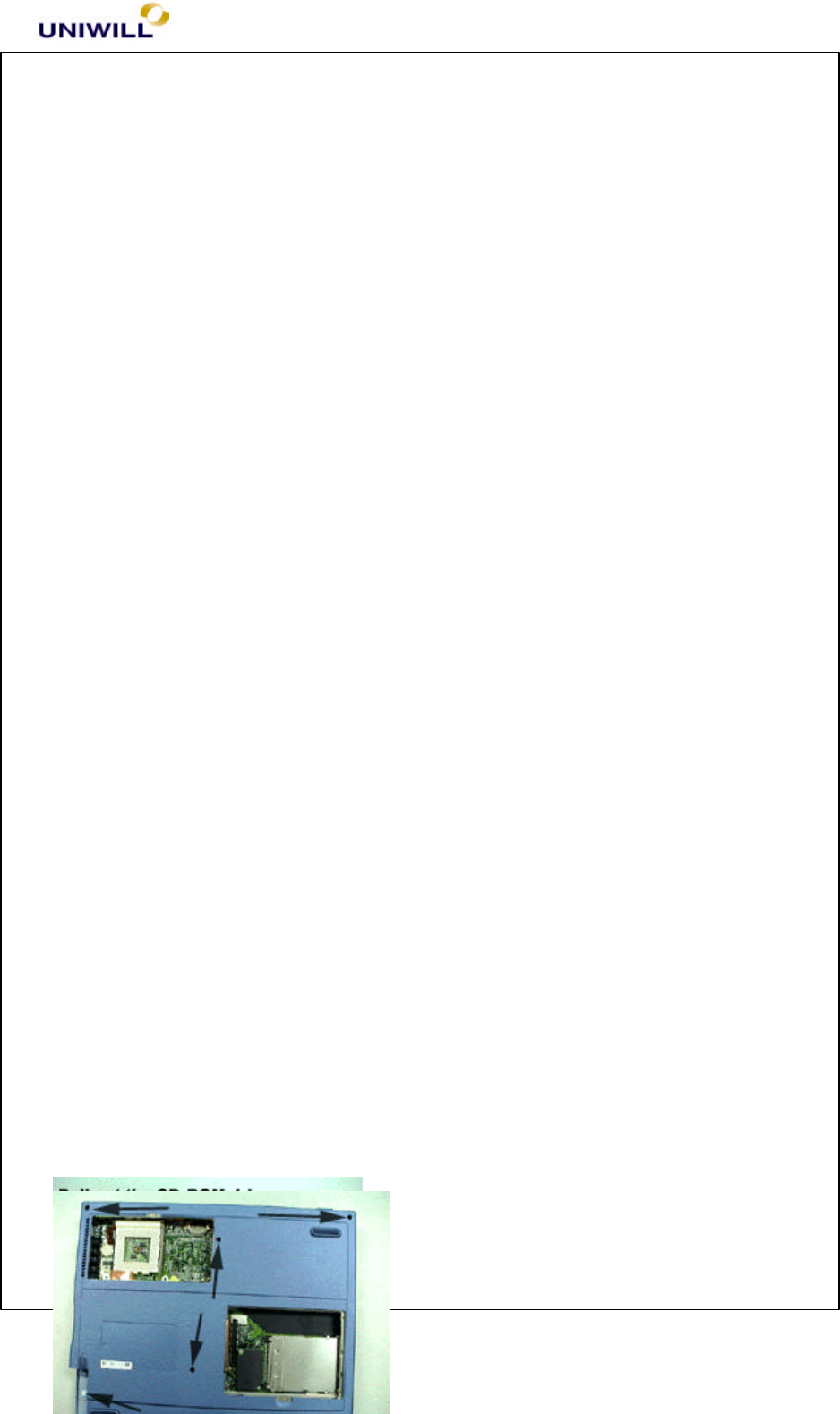
17. On the bottom case, push out the CD-ROM
drive as shown in the photo.
Chapter 5 Troubleshooting Guidelines
340S8 Rev : A Page
45
18. Unfasten six (6) screws on the bottom case.
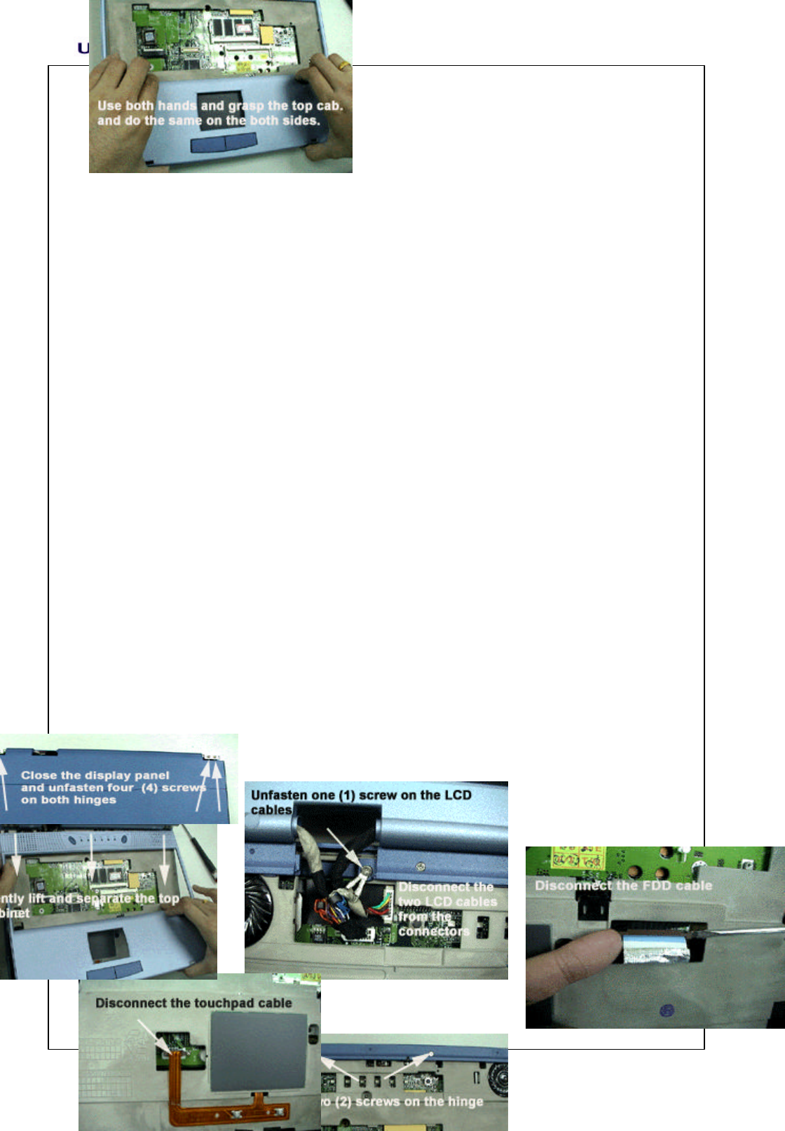
19. Grasp the top cabinet as shown in the photo and gently lift to release the snap lock. Do
the same procedure on both side of the top cabinet.
20. After releasing the snap lock on both side and palm rest. Lift up to release and remove the
top cabinet.
21. Close the display panel and unfasten four (4) screws on both sides of the display hinges.
Chapter 5 Troubleshooting Guidelines
340S8 Rev : A Page
46
22. Unfasten one (1) screw on the LCD cable and disconnect the two LCD cables from the
mainboard connectors.
23. Unfasten two (2) screws on the hinge frame as shown in the photo.
24. Disconnect the FDD cable.
25. Disconnect the Touchpad cable.
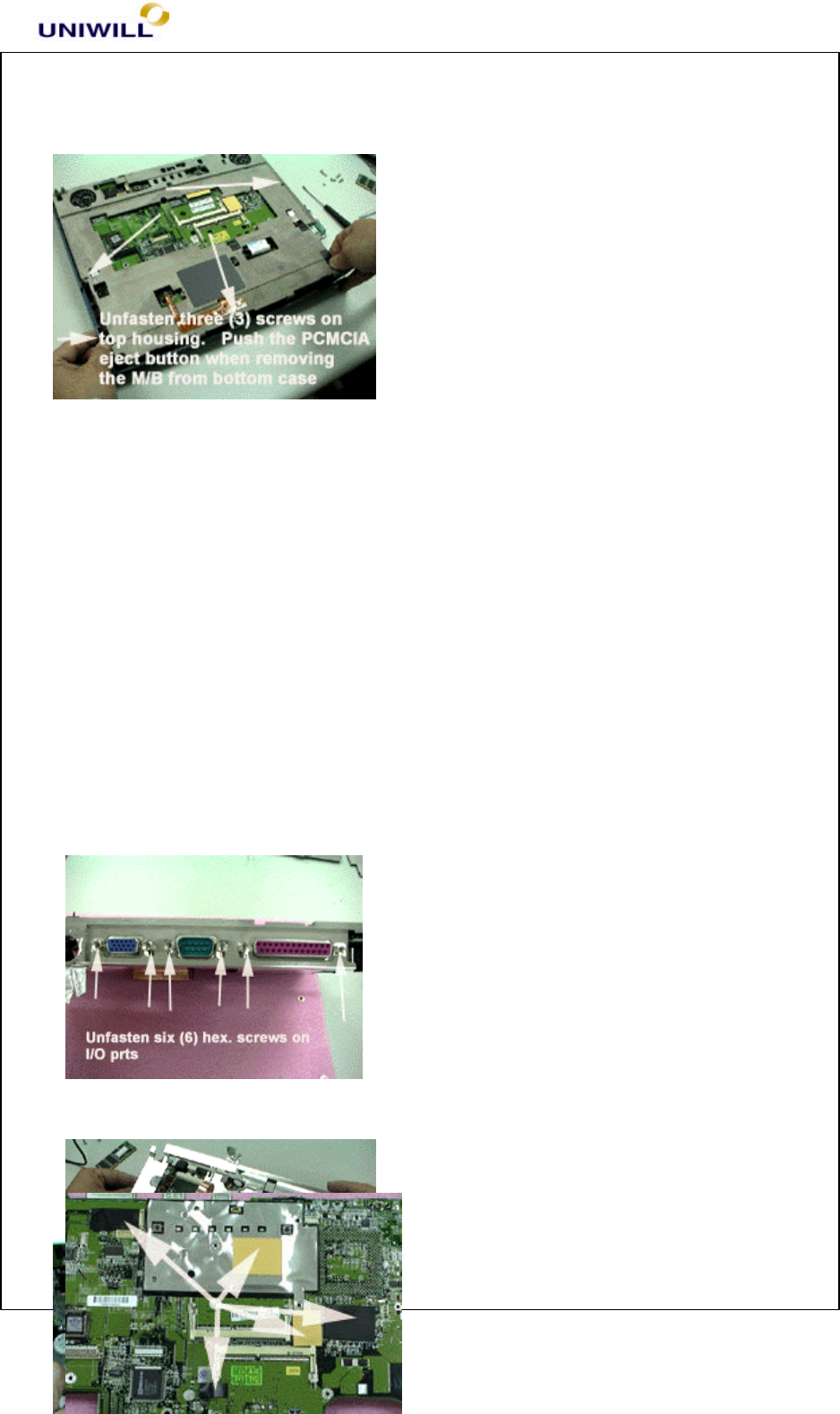
Chapter 5 Troubleshooting Guidelines
340S8 Rev : A Page
47
26. Unfasten three screws on the top housing ( Magnesium alloy). To remove the mainboard
together with the top housing, push in the
PCMCIA eject button and on the other hand, lift
the mainboard assembly and separate it from the
bottom case.
27. At the bottom side of the mainboard, unfasten
two (2) screws on the modem card. And
disconnect the modem card from the mainboard.
28. Unfasten the two (2) hexagonal screws of the modem card.
29. On the bottom side of the mainboard, unfasten four (4) screws on the mainboard shielding
and peel off the aluminum foil near the I/O port as
shown in the picture.
30. From the I/O port, unfasten six (6) hexagonal
screws on the I/O ports.
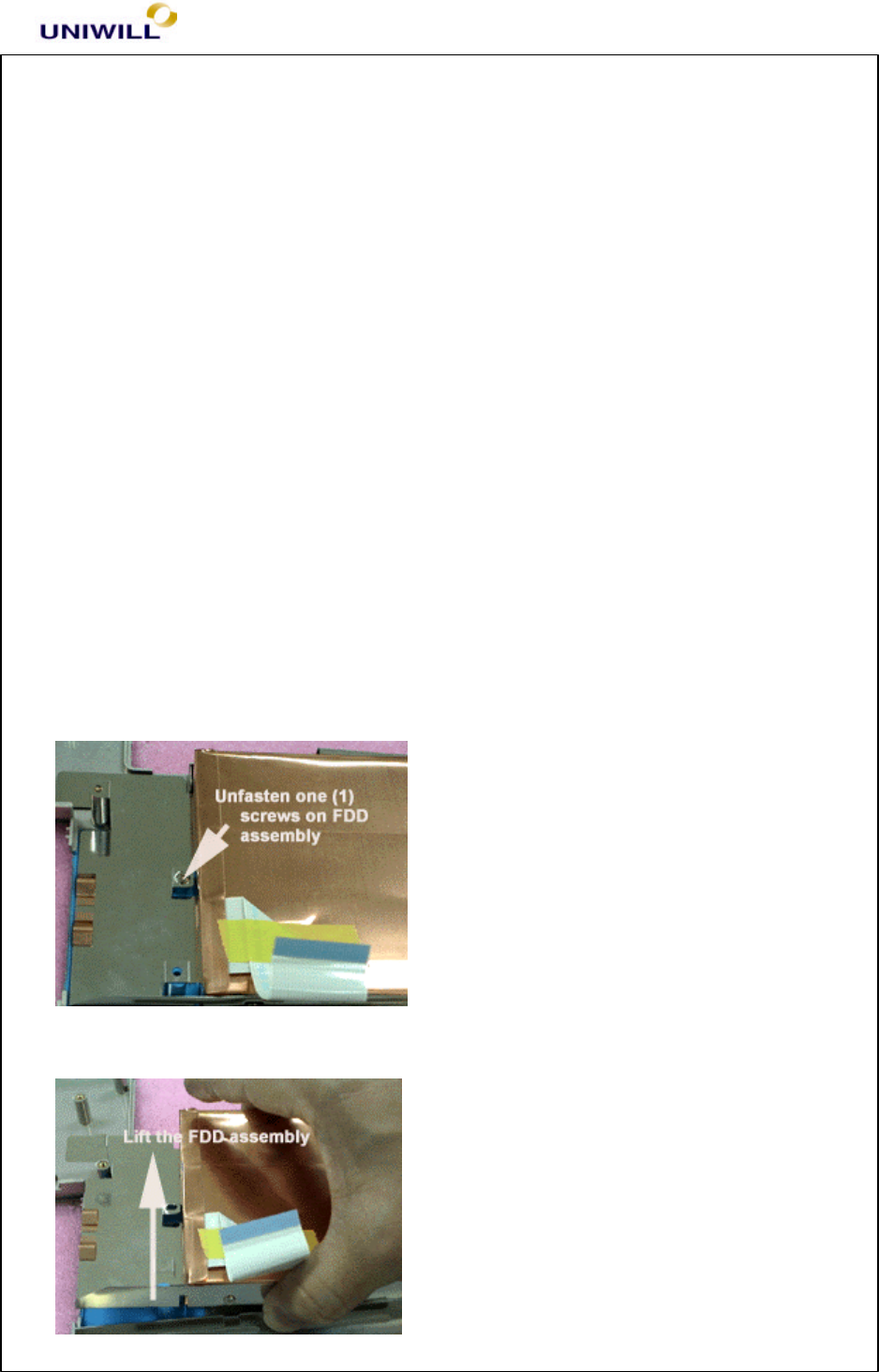
Chapter 5 Troubleshooting Guidelines
340S8 Rev : A Page
48
31. Starting from the I/O port portion, flip over the mainboard shielding.
32. Lift the mainboard and disconnect the speaker cable and LID switch cable.
33. When replacing mainboard, make sure to have all the insulation and thermal pads
removed from the defective mainboard and
transfer it to a good mainboard ( because
sometimes, the good mainboard doesn’t have
all the tapes and thermal pad as indicated in the
photo).

Chapter 5 Troubleshooting Guidelines
340S8 Rev : A Page
49
34. Unfasten one (1) screw on the FDD assembly.
Lift to remove the FDD assembly form the bottom case.
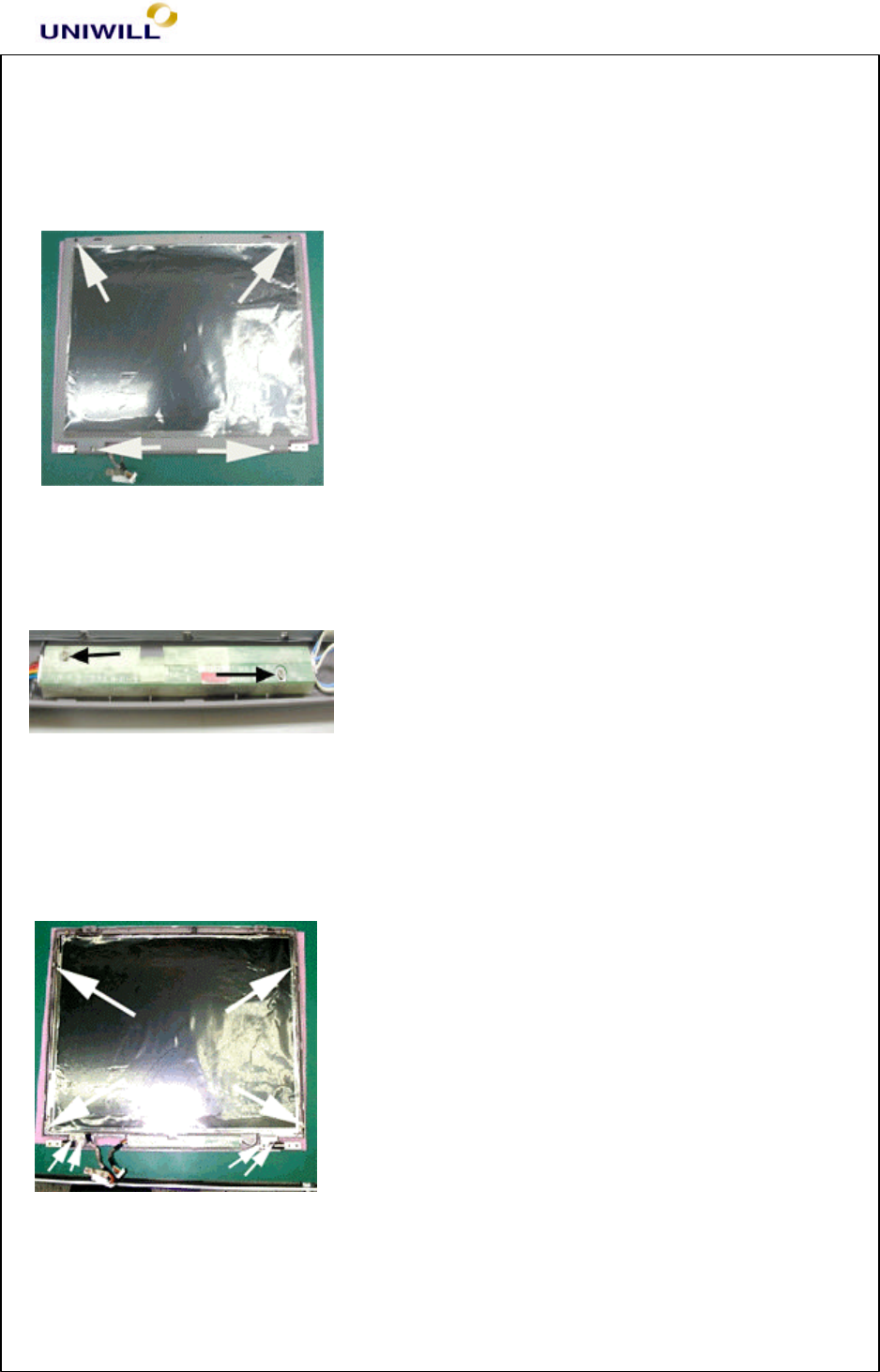
Chapter 5 Troubleshooting Guidelines
340S8 Rev : A Page
50
Display Disassembly Procedure
Chapter 5 Troubleshooting Guidelines
340S8 Rev : A Page
51
1. Remove the four rubber stopper on the front display cover and unfasten four (4) screws
underneath.
Grasp and remove the display front cover.
2. Unfasten two (2) screws on the D-A inverter card and disconnect the cables on both sides.
3. Unfasten four (4) screws on the LCD display and unfasten four (4) screws on both side of
the hinges.
Remove the LCD from the display cover.
Make sure to remember the LCD cable arrangement to avoid problem when assembling
the LCD display.

Chapter 5 Troubleshooting Guidelines
340S8 Rev : A Page
52
UNIWILL COMPUTER CORP.
No. 24, Pei Yuan Rd., Chung Li Industrial Park
Chung Li City, Taiwan, R.O.C.
TEL: 886-3-461-6000
FAX: 886-3-461-8000
URL: http://uniwill.com.tw/

Chapter 5 Troubleshooting Guidelines
340S8 Rev : A Page
53
Trouble Shooting List
5.1 No display
5.2 VGA controller failure
5.3 LCD no display / Invalid picture
5.4 External monitor has no display or color incorrect
5.5 Memory test error
5.6 Keyboard test error
5.7 Touch pad test error
5.8 Diskette drive test error
5.9 Hard disk drive test error
5.10 CMOS test error
5.11 SIO port test error
5.12 PIO port test error
5.13 Audio failure
5.14 No power symptom
5.15 CDROM drive test error
5.16 Stopping in LCD screen while booting
5.17 PCMCIA Card Bus failure
5.18 IR Port cannot transfer data
5.19 Modem Failure
Chapter 5 Troubleshooting Guidelines
340S8 Rev : A Page
54
5.1 No display (system failure)
Symptom: There is no display on both LCD and Monitor after power on although
the LCD and Monitor are known-good.
No Display
Monitor or LCD module ok?
Replace monitor or LCD
Display Ok?
Setup the display mode
Remove all of I/O device & cables from M/B except LCD or Monitor
Display ok
Replace motherboard
Board level troubleshooting
Check system clock and reset circuit
No
Yes
Yes
No
No
Yes
Check SIS Chipset for
any cold solder? Re-solder
No
Correct the I/O device & cables to the
M/B one at a time to find out which
part is ca
using the problem
Set up Display type in
BIOS
Yes
Chapter 5 Troubleshooting Guidelines
340S8 Rev : A Page
55
5.2 VGA controller failure
Symptom: There is no display on both LCD and Monitor although Power-On-
Self-Test is passed
VGA Controller Failure
Try another good monitor or LCD module
Replace faulty LCD or monitor
Display OK
Remove all of I/O devices and cables from M/B except LCD or Monitor
Connect the I/O device & cables to the M/B one per
time to find out which part is causing the problem
Display OK
Replace Motherboard
Board level troubleshooting
Yes
No
Yes
No
Yes
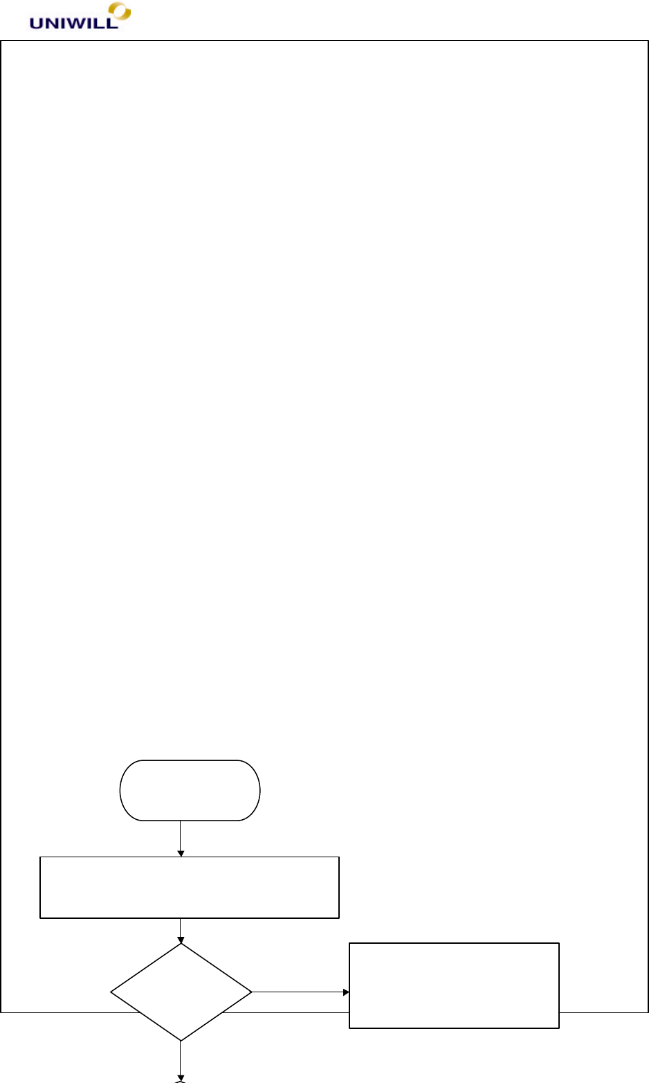
Chapter 5 Troubleshooting Guidelines
340S8 Rev : A Page
56
5.3 LCD no display or Invalid Picture
Symptom: The LCD shows nothing or abnormal picture, but it is ok for external
monitor.
LCD No Display
Try another known good LCD module
Display
OK?
No
Yes Replace each parts of LCD
module / cables and test

Chapter 5 Troubleshooting Guidelines
340S8 Rev : A Page
57
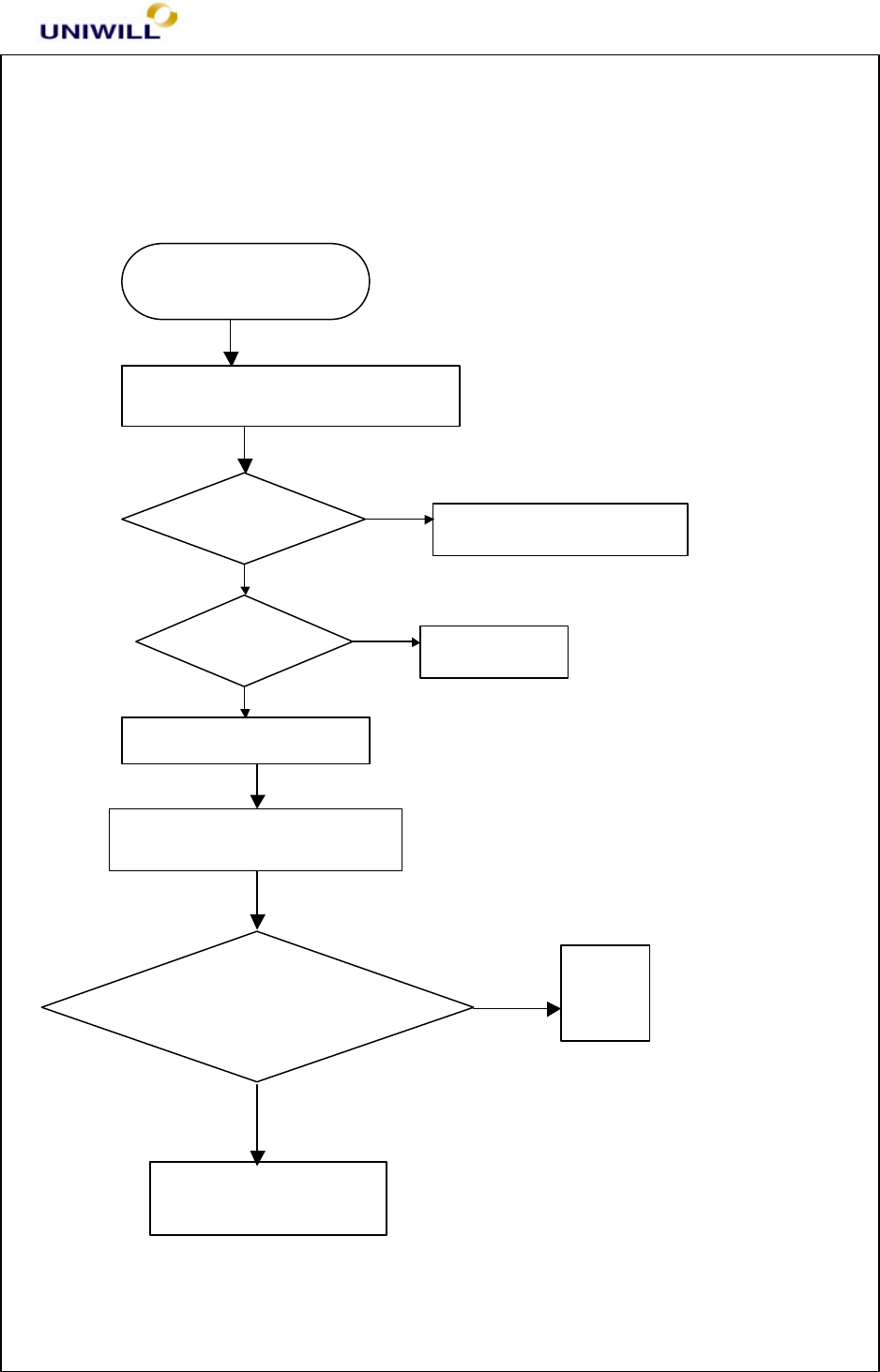
Chapter 5 Troubleshooting Guidelines
340S8 Rev : A Page
58
5.4 External monitor has no display or color abnormal
Symptom: The CRT monitor shows nothing or abnormal color, but it is ok for
LCD
Yes
No
Monitor No Display
Try another known good monitor
Replace faulty monitor
Correct it
Display Ok?
Setup Ok?
Replace motherboard
Board level Troubleshooting
Yes
No
Yes
No
Yes
Check VGA port signal
using oscilloscope
Replace SIS 630
Chipset
End
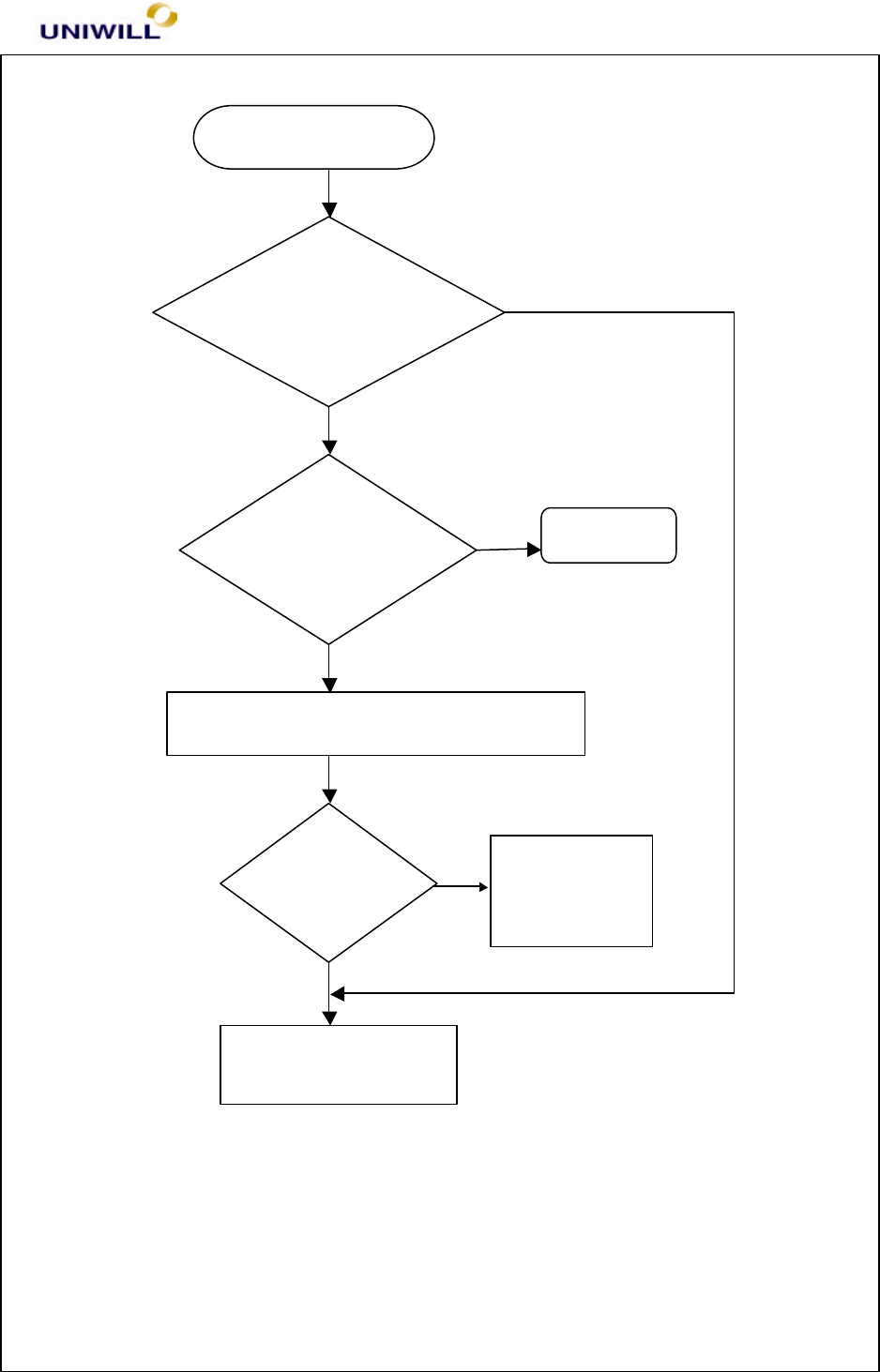
Chapter 5 Troubleshooting Guidelines
340S8 Rev : A Page
59
5.5 Memory test error
Memory test error
Try another known good DRAM module
Test OK?
Replace the
faulty DRAM
module
Replace motherboard
No
Yes
With External
DRAM Module
Installed?
Correct it
Install External
DRAM module
and socket OK?
Yes
No
Yes
No
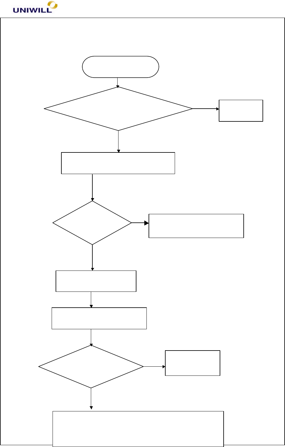
Chapter 5 Troubleshooting Guidelines
340S8 Rev : A Page
60
5.6 Keyboard test error (including external K/B & PS/2 mouse)
Symptom: error message of keyboard failure is shown or any key doesn’t work
Keyboard test error
Correct it
Is K/B cable connected to
M/B properly?
Try another good keyboard
KB Test
Ok?
Replace the faulty keyboard
Replace motherboard
Board level troubleshooting
Re-soldering
One of the following parts or signals on the other
board may be defective, use an oscilloscope to check
1.K/B Controller PC87570
Check for cold
solder?
No
Yes
No
Yes
No
Yes
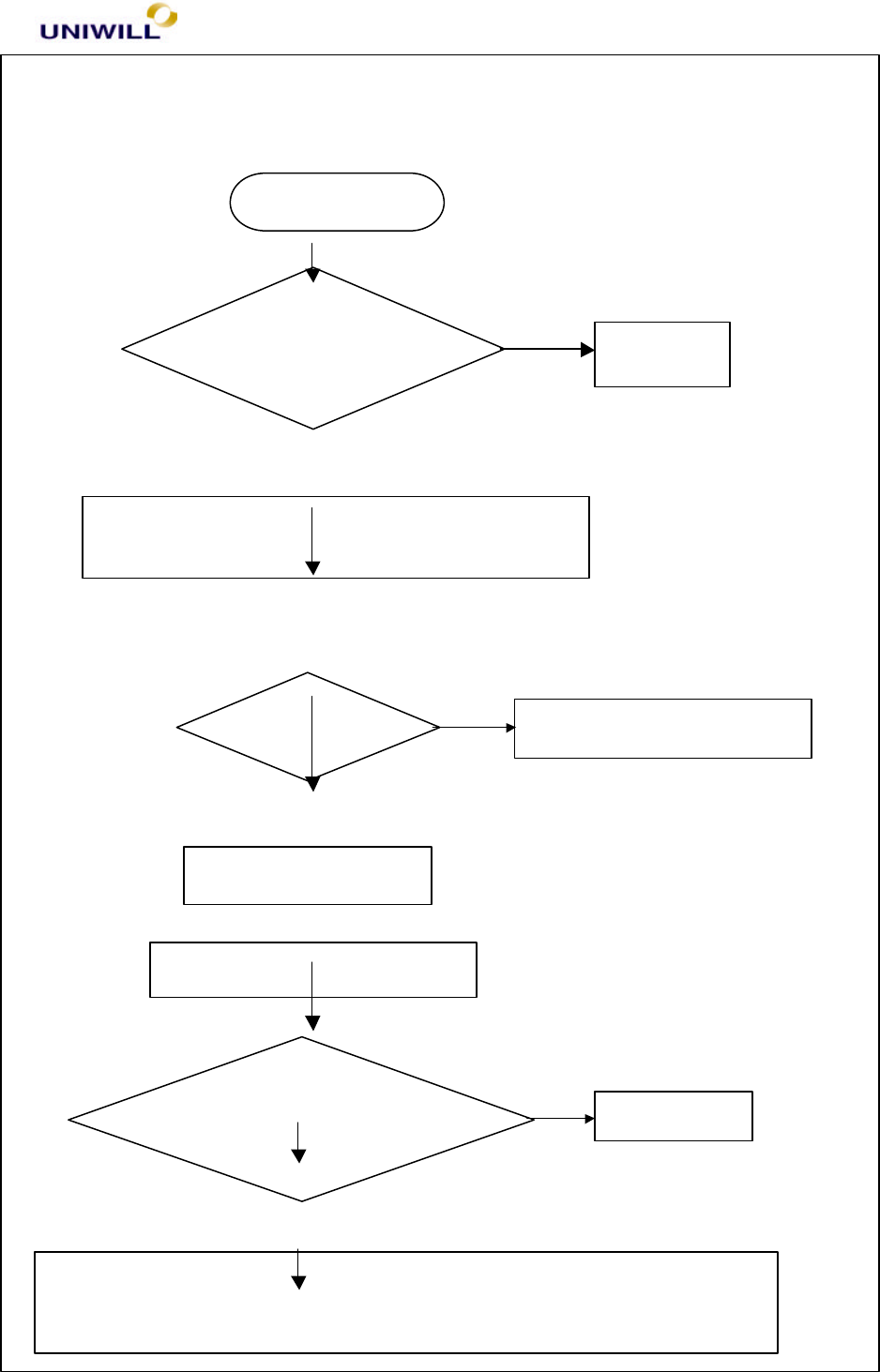
Chapter 5 Troubleshooting Guidelines
340S8 Rev : A Page
61
5.7 Touch Pad test error
Symptom: An error message is shown when the Touch Pad point is enabled
Touch pad error
Correct it
Is Touch pad cable
connected properly ?
Try another known good touch pad module and
cable
Test Ok ? Replace the faulty parts
Replace motherboard
Board level troubleshooting
Check KB controller
PC87570 for cold solder? Re-solder
No
Yes
No
Yes
No
Yes
Check one of the following parts or signals on the motherboard maybe
defective, use an oscilloscope and replace it.
1. KB Controller
–
PC87570
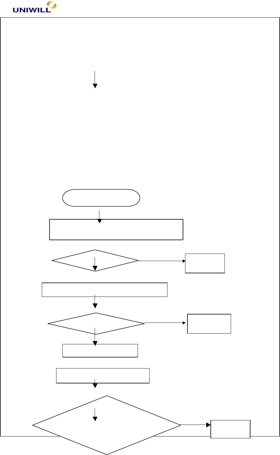
Chapter 5 Troubleshooting Guidelines
340S8 Rev : A Page
62
5.8 Diskette drive test error
Symptom: An error message is shown while loading data from FDD to system
Correct it
Reboot OK?
Try another known good FDD module
Reboot OK?
Replace motherboard
Board level troubleshooting
Check FDD connector,
Super I/O controller
PC87393 for cold solder?
Re-solder
No
No
Yes
Yes
No
Yes
Correct it
1. Try another known good boot diskette
2.
Check setup for correct settings
Diskette Drive test error
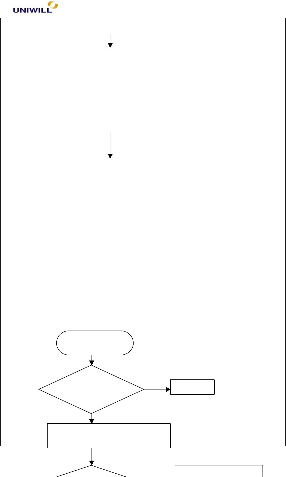
Chapter 5 Troubleshooting Guidelines
340S8 Rev : A Page
63
5.9 Hard disk drive test error
Symptom: Either an error message is shown, or the drive motor spins non-stop,
while reading data from or writing data to Hard disk
Hard disk test error
Replace the faulty parts
Re
-
boot ok?
Yes
Try another working HDD
Check BIOS
HDD Setup OK?
Correct it
Yes
No

Chapter 5 Troubleshooting Guidelines
340S8 Rev : A Page
64
5.10 CMOS test error
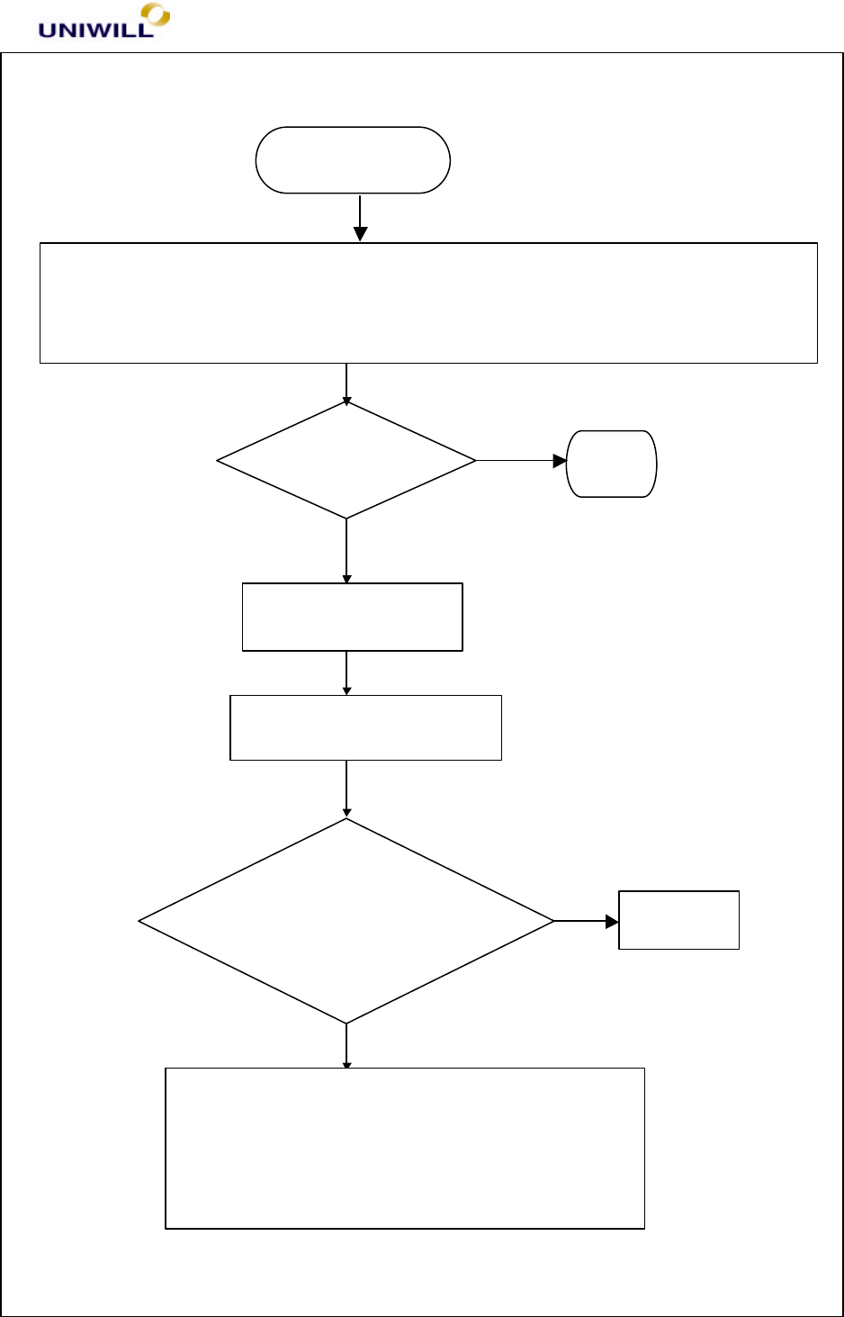
Chapter 5 Troubleshooting Guidelines
340S8 Rev : A Page
65
CMOS test error
1. Plug in AC adapter, power on the system and set correct data in BIOS setup
2. Keep the system power on for 8 hrs. to fully charge the RTC battery
3. Turn off power for 1 hour then turn on again
Re-boot OK? END
Board level troubleshooting
Replace motherboard
Check CMOS RAM,
CMOS battery for
cold solders
Re-solder
1. CMOS data lost, or inaccurate system time & data
Yes
Yes
One of the following parts on the motherboard
maybe defective, replace the parts one a time and
test after each replacement:
1.CMOS RAM 2. CMOS battery
No
No
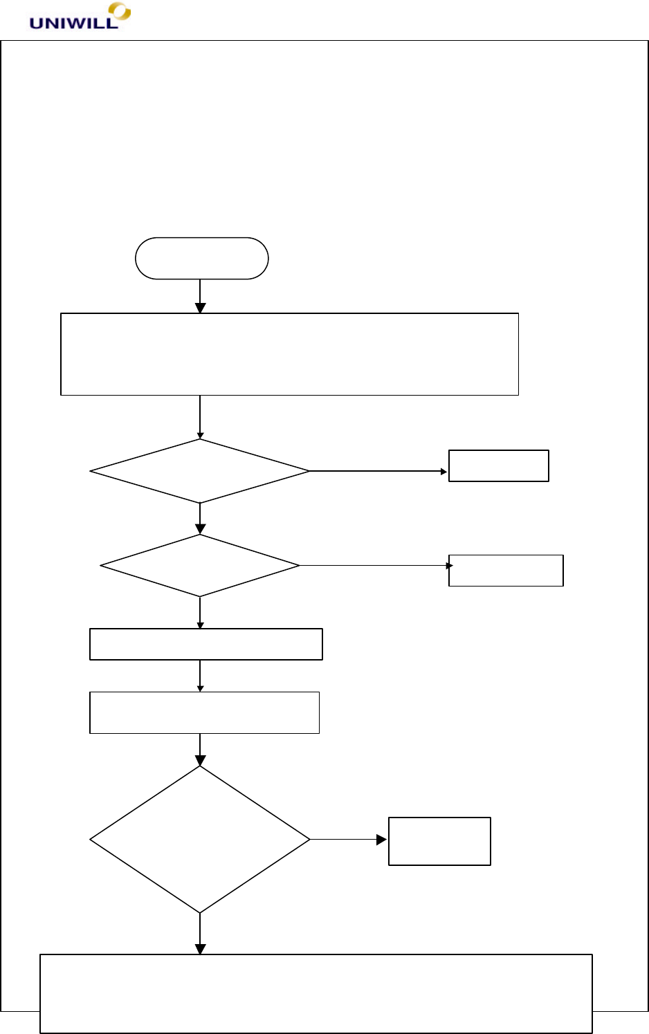
Chapter 5 Troubleshooting Guidelines
340S8 Rev : A Page
66
5.11 SIO port test error
Symptom: An error display occurs when a mouse or other I/O device is installed
SIO test error
Re-test Ok?
Setup OK?
Correct it
Correct it
Board level troubleshooting
Replace Motherboard
Check SIO
controller for
cold solder?
Re-solder
One of the following parts on the motherboard maybe defective, plug SIO
loopback at SIO port and run SIO test program. If error, replace SIO controller
No
Yes
Yes
Yes
No
No
1. Check whether mouse or other I/O device are properly
installed (including driver)
2.
Try another working mouse of I/O devic
e

Chapter 5 Troubleshooting Guidelines
340S8 Rev : A Page
67
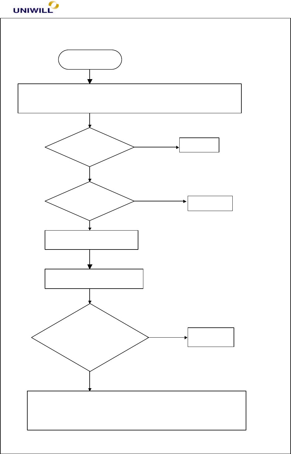
Chapter 5 Troubleshooting Guidelines
340S8 Rev : A Page
68
5.12 PIO port test error
Symptom: When a print command is issued, printer prints nothing or garbage.
PIO test error
1. check whether cables, printer & printer driver are installed properly
2. try another working printer and cable
Correct it
Re-test OK?
Setup OK?
Correct it
Board level troubleshooting
Replace motherboard
Check PIO
controller, for
cold
solder?
Re-solder
No
Yes
Yes
Yes
No
No
One of the following parts on the motherboard maybe defective, plug
PIO loopback at PIO port one a time and test, if error replace PIO
controller
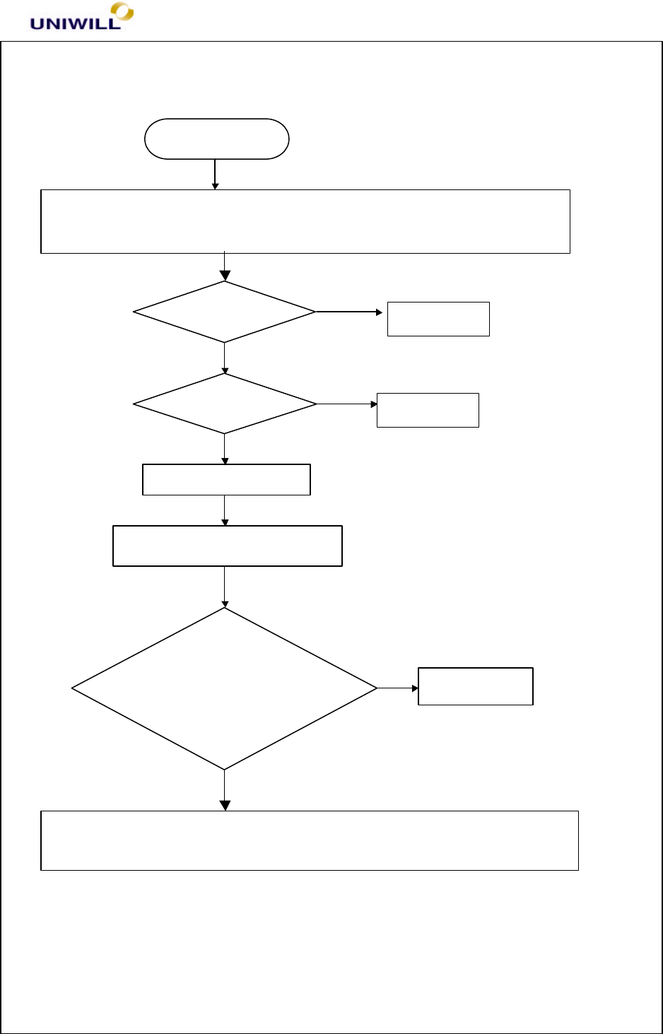
Chapter 5 Troubleshooting Guidelines
340S8 Rev : A Page
69
5.13 Audio failure
Symptom: No sound from speaker after audio drive is installed.
Audio test error
1. check whether cables, speakers & audio drivers are installed properly
2. try another working speaker & cable
Correct it
Re-test ok?
Setup ok?
Replace motherboard
Board-level troubleshooting
One of the following parts on the motherboard may be defective, replace
the audio controller chip
Yes
No
No
Yes
No
Correct it
Check SIS 630
Chipset for cold
Solder
Re-soldering
Yes
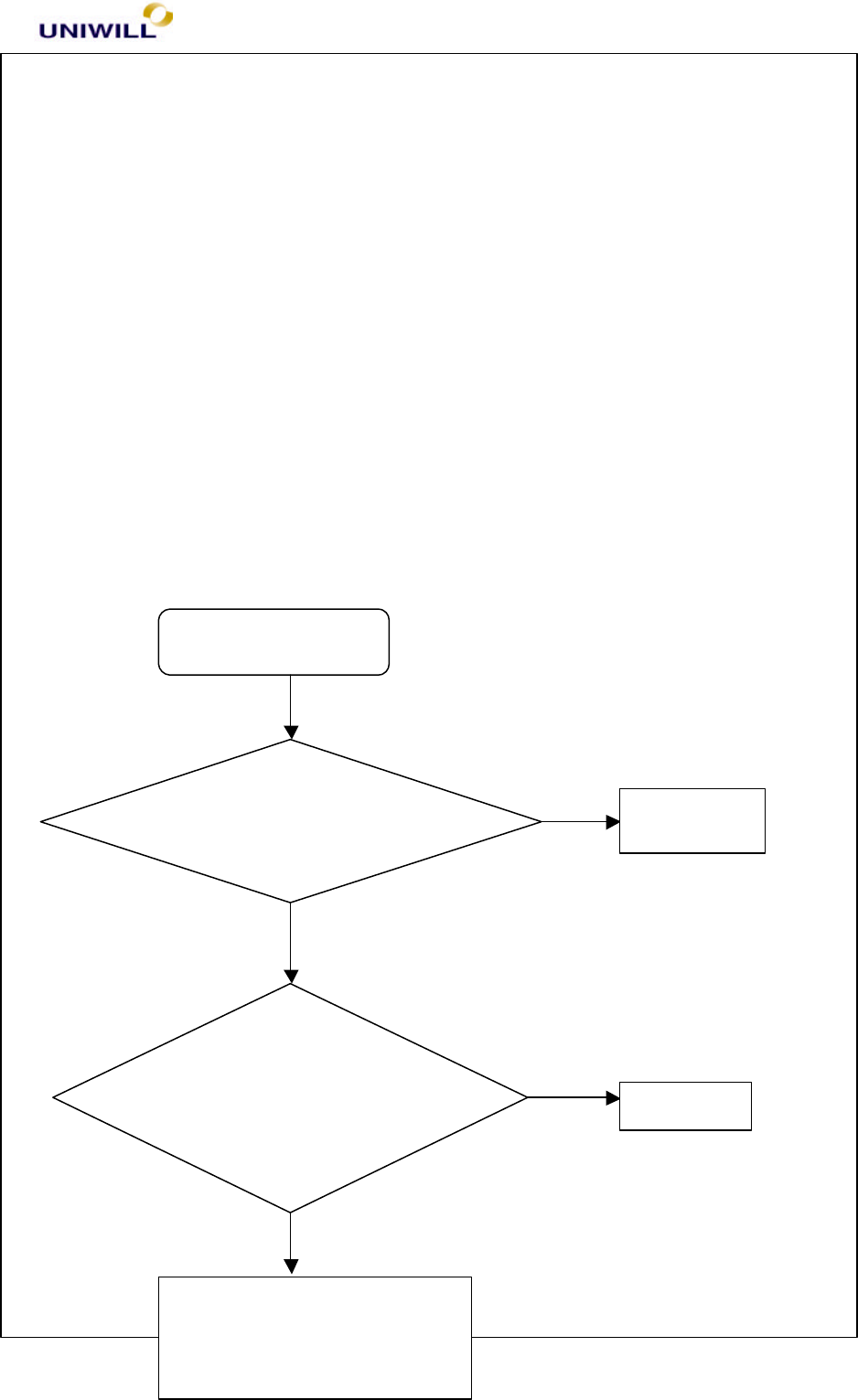
Chapter 5 Troubleshooting Guidelines
340S8 Rev : A Page
70
5.14 No power symptom:
Symptom: When the power button is pressed, nothing happens, power indicator
is not light up.
Check DC/DC Board
Signal or replace each
parts. Correct it
Press Power on button again
Check system LED lit on
Check Fuse on DC/DC
Board if open
No Power
Replace it
Yes
No
Yes
No
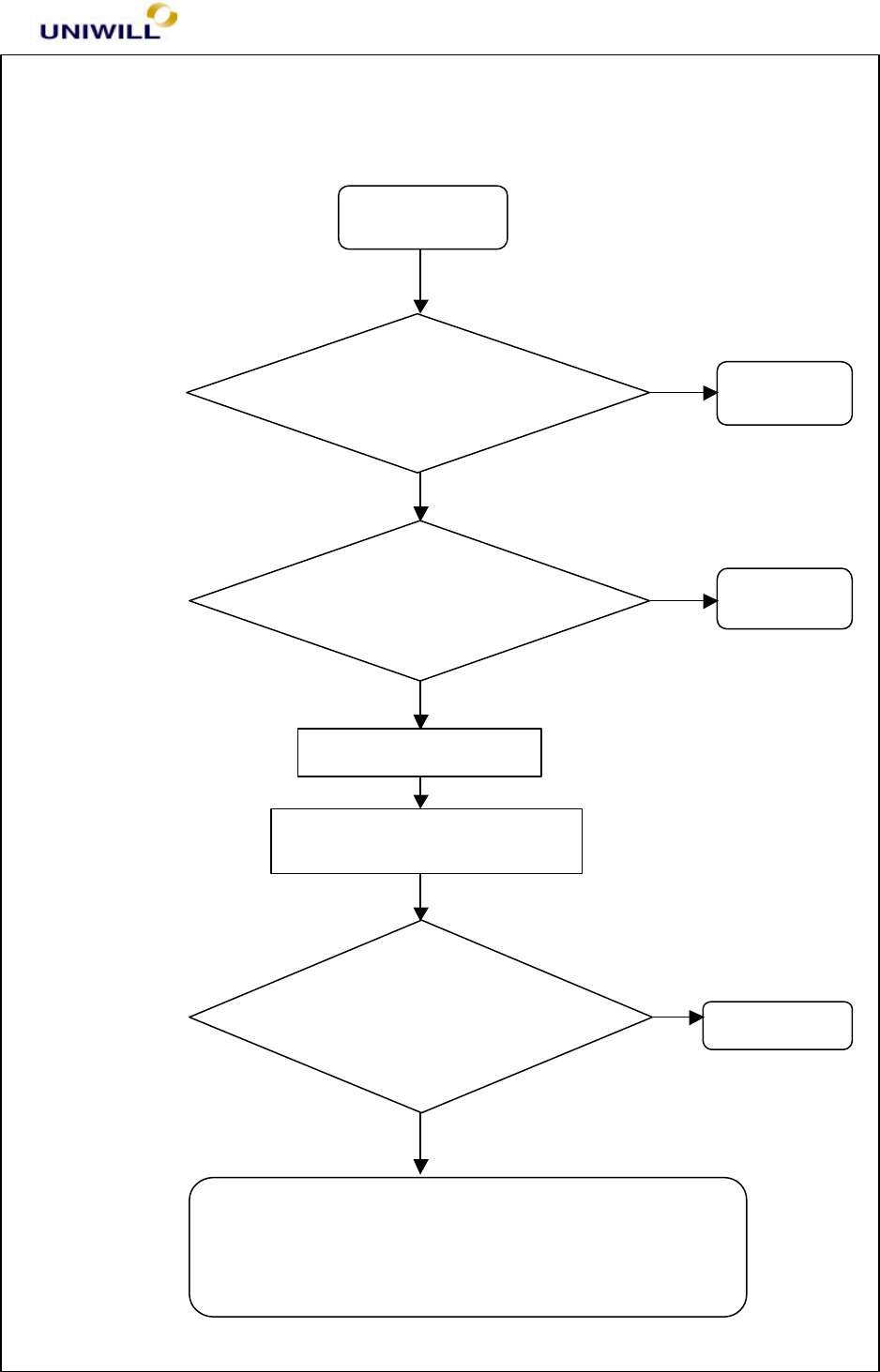
Chapter 5 Troubleshooting Guidelines
340S8 Rev : A Page
71
5.15 CD-ROM drive test error
An error message is shown when reading data from CD-ROM drive
Check drive is install
OK?
Check cable & Door is
closed
Correct it
Correct it
Re-soldering
Check one of the following parts or signal on the M/B
may be defective, use an oscilloscope to check it.
CDROM Failure
No
Yes
Yes
Replace Motherboard
Board Level Troubleshooting
No
Check SIS 630 Chipset
and CDROM connector
for cold solder?
Yes
No
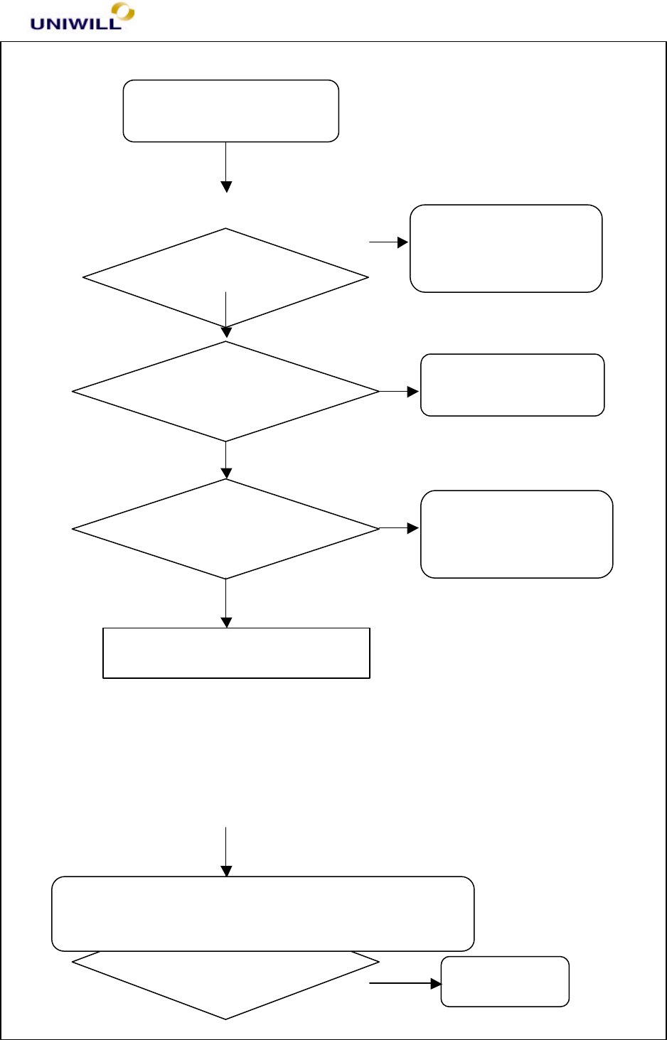
Chapter 5 Troubleshooting Guidelines
340S8 Rev : A Page
72
5.16 Stopping in LCD screen while booting
Check Memory
Size is correct?
Check HDD detection
is OK?
Check CD-ROM
Detection is OK?
Record LCD message &
to Board–level
Troubleshooting
Make sure HDD is good
&Check BIOS setting
Make sure CD-ROM
Is good & Check BIOS
Settings
Re-soldering
No
Yes
No
Yes
No
Yes
Stop in LCD screen while booting
Stop in LCD Screen while
booting
Check CPU &
SIS630 for cold
soldering? OK?
Check one of the following parts or signal on the M/B
may be defective, use an oscilloscope to check it. No
Yes
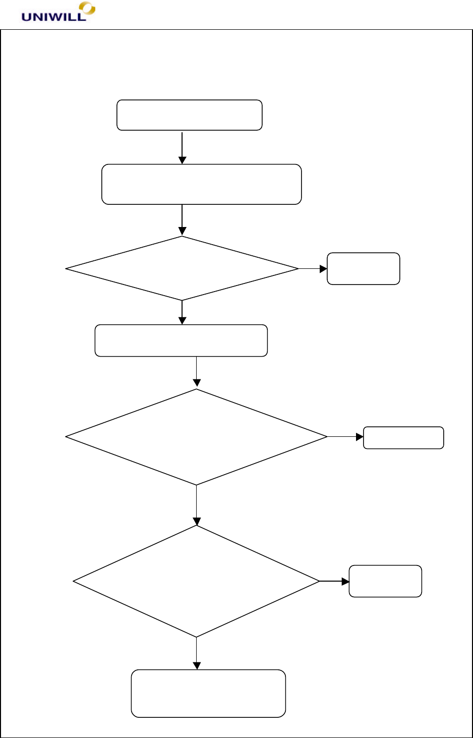
Chapter 5 Troubleshooting Guidelines
340S8 Rev : A Page
73
5.17 PCMCIA CardBus failure
Symptom : when insert PCMCIA card to PCMCIA slot, but system can’t
detect.
Re-soldering
PCMCIA card failure
Insert PCMCIA card completely again,
make sure good connection.
Check drive &
controller install OK?
Correct it
Board-level Trouble shooting
Check PCMCIA slot
mounting in M/B is cold
soldering
Check O2Micro OZ
6812 Chipset for cold
soldering?
Re-solder
Replace O2Micro OZ6812
chipset
No
Yes
Yes
No
Yes
No
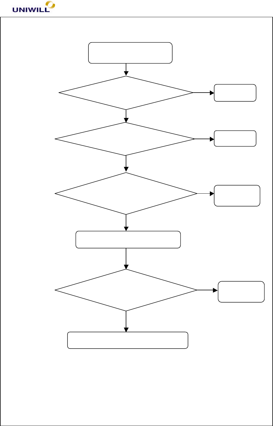
Chapter 5 Troubleshooting Guidelines
340S8 Rev : A Page
74
5.18 IR Port can’t transfer data.
IR failure & no response
Check driver install OK
Check another one IR
device is meet IrDa 1.0
Board-level trouble shooting
Check PC87393 for cold
soldering
Correct it
Try another IR
device
Re-soldering
Replace Super I/O PC97393 Chipset
Check BIOS setup
OK?
Correct it
No
Yes
No
Yes
No
Y
es
Yes
No
340S8 Rev : A Page 75
5.19 Modem failure
Modem Failure
Check Driver install &
Telephone Line is OK?
Check IRQ, COM port
setting is OK?
AT command test
modem function is OK
Board-level trouble shooting
Replace another known good modem
DAA module.
Correct it
Correct it
Re-install Drivers
Connect it
No
Yes
No
No
Yes
Check modem DAA board is
connected properly and
wiring with the phone jack
No
Yes
340S8 Rev : A Page 76
UNIWILL COMPUTER CORP.
No. 24, Pei Yuan Rd., Chung Li Industrial Park,
Chung Li City, Taiwan, R.O.C.
TEL: 886-3-461-6000
FAX: 886-3-461-6317
URL: http://www.uniwill.com.tw/

340S8 Rev : A Page 77
6.1 LCD
I. 14.1” TFT, XGA - Vendor – UNIPAC, CHI MEI,
II. 13.3” TFT, XGA – Vendor – ACER, IMES
III. 12.1” TFT, SVGA – Vendor – Sanyo, Torisan
6.2 FDD
Internal FDD: 3.5” format
Capacity : 720KB / 1.44MB / 1.2MB (3 mode)
Vendor : TEAC or MITSUMI
6.3 HDD
Dimension : 2.5”, 8.5 / 9.5 mm height
Vendor : Toshiba, and Fujitsu
6.4 CD-ROM
Vendor : QMATE, TEAC
Dimension : 12.7-mm height, 12/8 cm CD-ROM disc
PIO Mode 4, 24X
Average 3.1W, Sleep 0.05W
ATAPI Interface
DVD
Vendor : TORISAN, TOSHIBA, QMATE
Dimension : 12.7mm height, 12/8cm CD-ROM disc
PIO Mode 4
Average 3.1W, Sleep 0.05W
ATAPI Interface
6.5 BATTERY:
Li-ION
Vendor : PANASONIC , GS
Battery type : Li-Ion, 8 cells (4S2P)
Battery capacity : 14.8V, 3600mAH, (47.36Whrs)
1.1.1. Charge Voltage : 16.8V +2.5% -1.0%
Charge temperature : 0~45oC
Discharge temperature : -20~60oC
End of Discharge : 11V
Cycle life= 500 times
Overcharge protection : when battery voltage reach 17.2 ±0.2V
Over-discharge protection : when battery voltage decrease to 10 ± 1V
Pre-charge current: 0.2A
Charge current : When system is power off : 2A
When system is powered ON : 1A
Ni-MH
Vendor : PANASONIC, TOSHIBA
Battery Type : Ni-MH, 10 cells (10S)
Battery Capacity : 12.0V, 4500mAh (54.0 watts)
Charge voltage : 16.8V +2.5% -1.0%
Charge temperature : 0~45oC

340S8 Rev : A Page 78
Discharge temperature : -20~60oC
End of Discharge : 10V
Cycle life= 500 times
Pre-charge current: 0.2A
Charge current : When system is power off : 2A
When system is powered ON : 1A
6.6 TOUCH PAD
Synaptic
Capacitor sensor
Support edge motion
Support virtual scroll bar
Support 2 or 3 button mode
ESD withstand: 15KV
Power Consumption: 2.75mA / 5V
X/Y resolution: 500 points/inch
Interface: PS/2
6.7 KEYBOARD
Supplier : KC Matrix-290
Travel : 3.0 ±0.2mm
Support : 3 window keys
Key pitch : 19mm
Dimension : 249mm x 100.85mm x 7.8 mm
6.8 MODEM/FAX MODULE
Modem chip : SamrtLink HAMR5603+Si3014
Meet PC99 Window modem requirement
Support :
AMR / MDC slot / V.90 (56kbps) /AC’97 2.1 / APM & ACPI
V.34bis (4.8Kbps to 33.6Kbps) /
V.32 bis (4.8Kbps to 14 Kbps) /AT command set
V.42 (LAPM) and MNP 2-4 error correction, 5 data compression
V.22 bis ( 50 bps to 2.4Kbps) / V.21 Bell 103 / Bell 212
Fax Group3 Class 1/V.17, V.29, V.27ter, V.21 ch2/
Group III fax / telephony answering machine / DTMF generation and detection
Local handset, telephone and microphone record / telephone line and headset or
Peaked playback / VOX voice Detection/ Caller ID (optional) / host base DSVD
340S8 Rev : A Page 79
UNIWILL COMPUTER CORP.
No. 24, Pei Yuan Rd., Chung Li Indistrial Park
Chung Li City, Taiwan,R.O.C.
TEL: 886-3-461-6000
FAX: 886-3-461-6317
URL: http:// uniwill.com.tw/
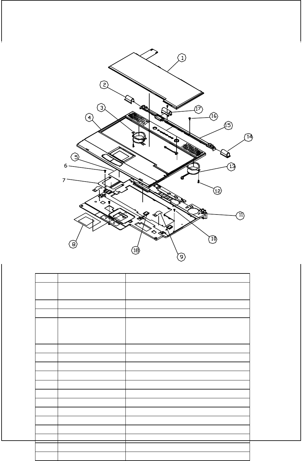
340S8 Rev : A Page 80
7.1 TOP CABINET ASSEMBLY
NO. PART NUMBER DESCRIPTION
1 71-002941-00
71-002933-00 K/B (GR) Blue
K/B (GR) Gray
2 50-352968-00 COVER HINGE (L) 340
3 40-102902-00 SPRING SPK 340
4
50-312942-00
50-312935-00
TOP CABINET
ID-2
ID-4
5 74-08U20400 T/P
6 41-720120-06 SCREW M2.0*6
7 29-163402-00 FPC T/P PAD
8 50-212904-00 ADHESIVE TAPE
9 40-102901-00 SPRING FOR K/B 340
10 41-720120-04 M2.0*4
11 50-312903-10 TOP HOUSING (MG) 340
12 41-720120-03 M2.0*3
13 22-300513-10 SPK FG-36N081
14 50-352967-00 COVER HINGE (R ) 340
15 50-352966-00 COVER HINGE FRAME
16 41-720120-03 M2.0*3
17 50-352969-00 COVER CABLE FOR 340
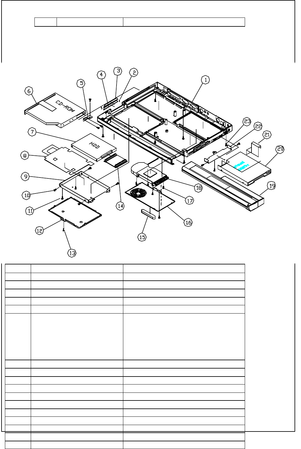
340S8 Rev : A Page 81
18 50-U34091-00 LATCH K/B FOR (BLOCK)
7.3 BASE CABINET ASSEMBLY
NO. PART NUMBER DESCRIPTION
1 50-U69022-70 BOTTOM CAB ASSY W/OUT TV OUT
2 40-102904-00 SPRING PCMCIA DOOR
3 50-206000-00 DOOR PCMCIA (U) 340
4 50-206001-00 DOOR PCMCIA (L) 340
5 40-302913-00 BRACKET CDROM 340
6 TEAC – 70-130104-00
QUANTA 70-130117-10
TORISAN – 70-200010-00
QUANTA – 70-200010-10
CD-ROM DRIVE
DVD-ROM DRIVE
7 xxx HDD
8 50-212902-00 MYLAR HDD 340
9 40-U75071-00 PLATE HDD 340
10 41-760230-03 SCREW M3.0*3
11 41-720120-04 SCREW M2.0*4
12 50-U69064-20 DOOR HDD 340
13 41-720120-04 SCREW M2.0*4
14 29U6905B-00 CABLE HDD 340
15 RUBBER FOOT 340
16 50-U69063-20 DOOR CPU 340
17 SCREW M2.5*4.5 PAN
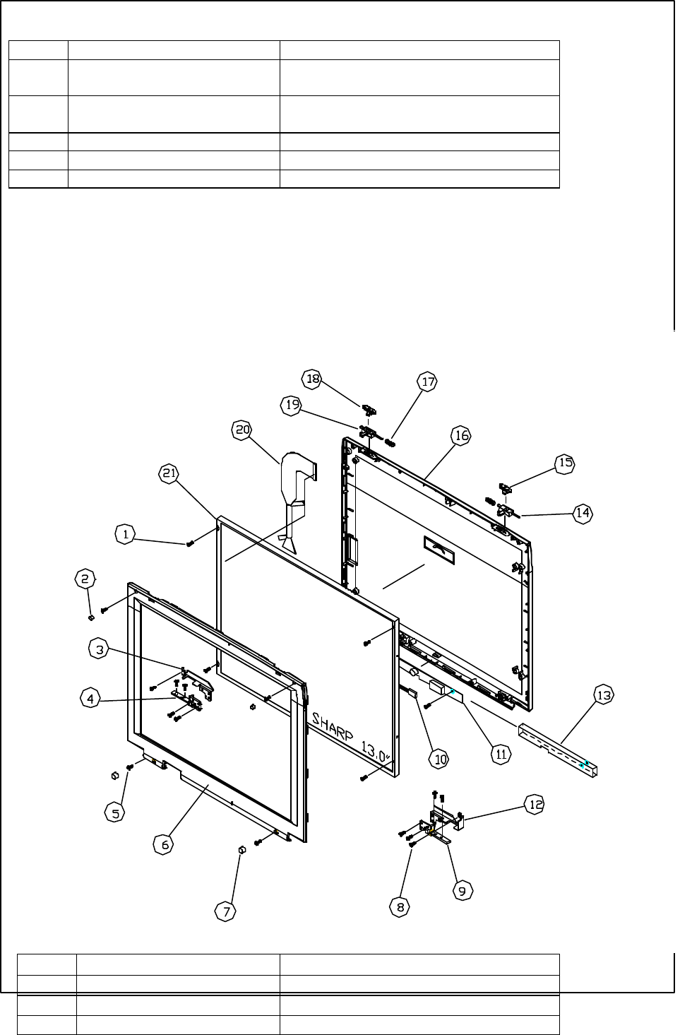
340S8 Rev : A Page 82
18 70-U69711-00 THERMAL MODULE FOR 340S8
19 3200MAH- 23-523200-40
3600MAH 23-U53600-03 BATTERY
20 MITSUMI – 70-013144-UC
TEAC -70-013144-U2 FDD
21 29-163403-00 FFC FDD
22 40-U69031-20 BRACKET FDD 340
23 41-720125-03 SCREW M2X0.45X8
7.4 LCD ASSEMBLY
NO. PART NUMBER DESCRIPTION
1 41-720525-06 SCREW M2.5*6
2 52-012919-00 RUBBER FOR DISPLAY (T) 340
3 40-U78021-00 BRACKET (L) FOR LCD
340S8 Rev : A Page 83
4 40-152907-00 HINGE (L) A-TYPE 340
5 41-720525-06 SCREW M2.5*6
6 ID-2
12.1” – 50-33931-00
13.3” - 50-332932-00
14.1” - 50-332930-00
ID-4
13.3” – 50-U34032-00
14.1” - 50-U78032-00
FRONT CAB
7 52-012920-00 RUBBER FOR DISPLAY (B)
8 41-720120-04 SCREW M2.0*4
9 40-152909-00 HINGE ( R) A-TYPE 340
10 13.3” - 29-102901-00
14.1” – 29-102901-00 CABLE FOR LCD INVERTER
11 14.1” – 76-030527-00 INVERTER FOR
12 x BRACKET ( R) FOR LCD
NO. DESCRIPTION
13 50-212900-00 MYLAR FOR INVERTER 340
14 50-242912-10 HOOK LCD (R ) 340
15 50-412913-00 KNOB LCD (340)
16 ID-2
12.1” – 50-342982-00
13.3” - 50-342981-00
14.1” - 50-342981-00
ID-4
13.3” – 50-342999-00
14.1” - 50-342900-10
BACK CABINET
17 40-101603-00 SPRING LCD GE-6200
18 50-412913-00 KNOB LCD 340
19 50-242912-00 HOOK LCD (L) 340
20 14.1” (uni ) – 29-U69051-00
14.1” (cmo) 29-U69051-00 CABLE FOR LCD
21 CMO 14.1 “ – 72-10014B-00
UNIPAK 14.1” –72-100149-00 LCD
