VPC CG9bk Cg9ex Sm
User Manual: VPC-CG9bk
Open the PDF directly: View PDF ![]() .
.
Page Count: 34
SERVICE MANUAL
Contents
1. OUTLINE OF CIRCUIT DESCRIPTION ............................... 3
2. DISASSEMBLY ................................................................... 12
3. ELECTRICAL ADJUSTMENT ............................................. 17
4. USB STORAGE INFORMATION REGISTRATION ............ 22
5. TROUBLESHOOTING GUIDE............................................ 23
6. PARTS LIST........................................................................ 24
CIRCUIT DIAGRAMS & PRINTED WIRING BOARDS........... C1
CAUTION : Danger of explosion if battery is incorrectly replaced.
Replace only with the same or equivalent type recommended by the
manufacturer.
Discard used batteries according to the manufacturer’s instructions.
NOTE : 1. Parts order must contain model number, part number, and description.
2. Substitute parts may be supplied as the service parts.
3. N. S. P. : Not available as service parts.
Design and specification are subject to change without notice.
SG214/U, EX, GX, EX2, GX2, EX4, GX5, U4, EX5 (R) REFERENCE No. SM5310742
FILE NO.
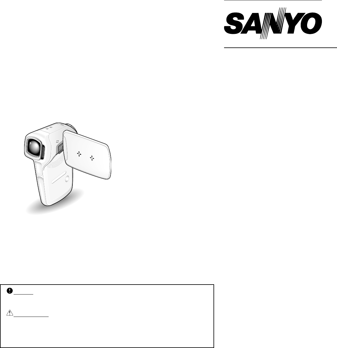
Digital Movie Camera
VPC-CG9BK
(Product Code : 168 137 02)
(U.S.A.) (Canada)
VPC-CG9EXBK
(Product Code : 168 137 03)
(Europe) (U.K.) (South America)
(China) (Australia) (Hong Kong)
(Russia) (Middle East) (Africa)
(General) (Korea) (Taiwan)
RoHS
•This product does not contain any hazardous substances prohibited by the RoHS
Directive.
WARNING
•You are requested to use RoHS compliant parts for maintenance or repair.
•You are requested to use lead-free solder.
(This product has been manufactured using lead-free solder. Be sure to follow the
warning given on page 2 when carrying out repair work.)
VPC-CG9GXBK
(Product Code : 168 137 04)
(South America) (China)
(Australia) (Hong Kong)
(General) (Korea) (Taiwan)
VPC-CG9EXW
(Product Code : 168 137 07)
(Europe) (U.K.) (South America)
(China) (Australia) (Hong Kong)
(Russia) (Middle East) (Africa)
(General) (Korea) (Taiwan)
VPC-CG9GXW
(Product Code : 168 137 09)
(South America) (China)
(Australia) (Hong Kong)
(General) (Korea) (Taiwan)
VPC-CG9EX
(Product Code : 168 137 11)
(Europe) (U.K.) (South America)
(China) (Australia) (Hong Kong)
(Russia) (Middle East) (Africa)
(General) (Korea) (Taiwan)
VPC-CG9GXP
(Product Code : 168 137 12)
(South America) (China)
(Australia) (Hong Kong)
(General) (Korea) (Taiwan)
VPC-CG9
(Product Code : 168 137 18)
(U.S.A.) (Canada)
VPC-CG9EXP
(Product Code : 168 137 19)
(Europe) (U.K.) (South America)
(China) (Australia) (Hong Kong)
(Russia) (Middle East) (Africa)
(General) (Korea) (Taiwan)

– 2 –
WARNING
Do not use solder containing lead.
This product has been manufactured using lead-free solder in
order to help preserve the environment.
Because of this, be sure to use lead-free solder when carrying
out repair work, and never use solder containing lead.
Lead-free solder has a melting point that is 30 - 40°C (86 -
104°F) higher than solder containing lead, and moreover it does
not contain lead which attaches easily to other metals. As a
result, it does not melt as easily as solder containing lead, and
soldering will be more difficult even if the temperature of the
soldering iron is increased.
The extra difficulty in soldering means that soldering time will
increase and damage to the components or the circuit board
may easily occur.
Because of this, you should use a soldering iron and solder
that satisfy the following conditions when carrying out repair
work.
Soldering iron
Use a soldering iron which is 70 W or equivalent, and which
lets you adjust the tip temperature up to 450°C (842°F). It
should also have as good temperature recovery characteris-
tics as possible.
Set the temperature to 350°C (662°F) or less for chip compo-
nents, to 380°C (716°F) for lead wires and similar, and to 420°C
(788°F) when installing and removing shield plates.
The tip of the soldering iron should have a C-cut shape or a
driver shape so that it can contact the circuit board as flat or in
a line as much as possible.
Solder
Use solder with the metal content and composition ratio by
weight given in the table below. Do not use solders which do
not meet these conditions.
Lead-free solder is available for purchase as a service tool.
Use the following part number when ordering:
Part name: Lead-free solder with resin (0.5 mm dia., 500 g)
Part number: VJ8-0270
Metal content Tin (Sn) Silver (Ag) Copper (Cu)
Composition
ratio by weight 96.5 % 3.0 % 0.5 %
Note:
If replacing existing solder containing lead with lead-free sol-
der in the soldered parts of products that have been manufac-
tured up until now, remove all of the existing solder at those
parts before applying the lead-free solder.
The components designated by a symbol ( ! ) in this schematic diagram designates components whose value are of
special significance to product safety. Should any component designated by a symbol need to be replaced, use only the part
designated in the Parts List. Do not deviate from the resistance, wattage, and voltage ratings shown.
PRODUCT SAFETY NOTICE
– 3 –
1. OUTLINE OF CIRCUIT DESCRIPTION
1-1. CMOS CIRCUIT DESCRIPTION
1. IC Configuration
The CMOS peripheral circuit block basically consists of the
following ICs.
IC911 (MT9N001I125TC)
CMOS imager
CDS, AGC, ADC built-in
H driver, V driver, serial communication circuit built-in
2. IC911 (CMOS)
[Structure]
The electric charges which are generated when each pixel is
optically converted are in turn converted into signal voltages
by the FD amplifier, and they are then transmitted by the built-
in H driver and V driver. The signals are sampled and ampli-
fied by the CDS and PGA circuits at the point they are output,
and then they are AD converted and output. The output uses
the 12 bit parallel interface.
1/2.3-inch positive pixel array CMOS-type fixed imaging ele-
ment
Effective pixels 3488 (H) X 2616 (V)
– 4 –
1-2. CP1 and VF1 CIRCUIT DESCRIPTION
1. Circuit Description
1-1. Digital clamp
The optical black section of the extracts averaged values from
the subsequent data to make the black level of the output
data uniform for each line. The optical black section averaged
value for each line is taken as the sum of the value for the
previous line multiplied by the coefficient k and the value for
the current line multiplied by the coefficient 1-k.
1-2. Signal processor
1. γ correction circuit
This circuit performs (gamma) correction in order to maintain
a linear relationship between the light input to the camera
and the light output from the picture screen.
2. Color generation circuit
This circuit converts the image sensor into RGB signals.
3. Matrix circuit
This circuit generates the Y signals, R-Y signals and B-Y sig-
nals from the RGB signals.
4. Horizontal and vertical aperture circuit
This circuit is used gemerate the aperture signal.
1-3. AE/AWB and AF computing circuit
The AE/AWB carries out computation based on a 64-segment
screen, and the AF carries out computations based on a 6-
segment screen.
1-4. SDRAM controller
This circuit outputs address, RAS, CAS and CS data for con-
trolling the SDRAM. It also refreshes the SDRAM.
1-5. Communication control
1. SIO
This is the interface for the 8-bit microprocessor.
2. PIO/PWM/SIO for LCD
8-bit parallel input and output makes it possible to switch be-
tween individual input/output and PWM input/output.
1-6. Digital encorder
It generates chroma signal from color difference signal.
2. Outline of Operation
When the shutter opens, the reset signals (ASIC and CPU)
and the serial signals (“take a picture” commands) from the
8-bit microprocessor are input and operation starts.
The picture data from CMOS passes through the A/D and
CDS, and is then input to the ASIC as digital data. The AF,
AE, AWB, shutter, and AGC value are computed from this
data, and three exposures are made to obtain the optimum
picture. The data which has already been stored in the SDRAM
is read by the CPU and color generation is carried out. Each
pixel is interpolated from the surrounding data as being ei-
ther R, G, and B primary color data to produce R, G and B
data. At this time, correction of the lens distortion which is a
characteristic of wide-angle lenses is carried out. After AWB
and γ processing are carried out, a matrix is generated and
aperture correction is carried out for the Y signal, and the
data is then compressed by JPEG and is then written to card
memory (SD card).
When the data is to be output to an external device, it is taken
data from the memory and output via the USB I/F. When played
back on the LCD and monitor, data is transferred from memery
to the SDRAM, and the image is then elongated so that it is
displayed over the SDRAM display area.
3. LCD Block
The LCD display circuit is located on the CP1 board and VF1
board, and consists of components such as a power circuit
and VCOM control circuit.
The signals from the ASIC are 8-bit digital signals, that is
input to the LCD directly. The 8-bit digital signals are con-
verted to RGB signals inside the LCD driver circuit. The LCD
is input signals from ASIC directly to the LCD, and function
such as image quality are controlled.
In addition, the timing pulses for signals other than the video
signals are also input from the ASIC directory to the LCD.
– 5 –
5. Video Clip Recording and Playback
5-1. Recording
The signal from the camera block is input to IC101 (ASIC). The
data that is input to the ASIC is input to SDRAM, and converts
this data to encoded MPEG4 data, after which it is written in
sequence onto the SD card as streaming data. At this time,
the audio signals that are input to the built-in microphone are
converted into digital data by the audio CODEC IC of IC183,
and they are then input to ASIC. The audio data is then en-
coded (AAC), and then it is written in sequence onto the SD
card together as streaming data with the image signals de-
scribed above.
5-2. Playback
The data is read from the SD card, and the encoded data is
decoded into image data where it is displayed by the LCD or
on a TV monitor. At the same time, the audio data is also de-
coded, and is input to IC183 as digital data. D/A conversion is
carried out at IC183, and the sound is then output to the speaker
or to the LINE OUT terminal or the headphone.
6. Audio CODEC Circuit (IC183)
The audio signals from the microphone are converted into 16-
bit digital data. AD conversion is carried out at a maximum
sampling frequency of 48 kHz.
During audio playback, the 16-bit digital data is converted into
analog signals and these drive headphone through the speaker
or line out system and headphone amplifier. DA conversion is
carried out at a maximum sampling frequency of 48 kHz.
4. Lens drive block
4-1. Focus drive
The 16-bit serial data signals (LENS_SD) and (LENS_SCLK
and LENS_EN) which are output from the ASIC (IC101) are
used to drive (FOCUS A +, FOCUS A -, FOCUS B + and FO-
CUS B -) by the motor driver IC (IC951), and are then used to
microstep-drive the stepping motor for focusing operation.
Detection of the standard focusing positions is carried out by
the ASIC detecting the signal (F_SENSE) from the
photointerruptor inside the lens block.
4-2. Zoom drive
The 16-bit serial data signals (LENS_SD) and (LENS_SCLK
and LENS_EN) which are output from the ASIC (IC101) are
used to drive (ZOOM A +, ZOOM A -, ZOOM B + and ZOOM B
-) by the motor driver IC (IC951), and are then used to
microstep-drive the stepping motor for zooming operation.
Detection of the standard zooming positions is carried out by
the ASIC detecting the signal (Z_SENSE) from the
photointerruptor inside the lens block.
4-3. ND filter
The ND filter drive signals (NDON and NDOFF) which are out-
put from the ASIC (IC101) are used to drive (ND + and ND -)
by the motor driver (IC951), and then the ND filter is inserted
into and removed from the beam path.
4-4. Iris drive
The drive method is a galvanometer type without braking coil.
The output from the Hall sensor inside the lens is amplified by
the Hall amplifier circuit inside the IC971 lens drive IC, and the
difference between the current and target aperture determined
by the resulting output and the exposure amout output from
the ASIC (IC101) is input to the servo amplifier circuit (IC971)
to keep the aperture automatically controlled to the target ap-
erture. The lens aperture control signal is output from IC971
and is input to lens drive IN6B of IC951. IC951 functions as
the driver for driving the lens.
4-5. Shutter drive
Reverse voltage is applied to the above aperture drive coil to
operate the shutter. When the shutter operates, the OC_EN
and OC_CONT signals are maintained at a high level, it is
input to IN6B of IC951 with low level.
At the same time the SHUTTER + signal that is output from
the ASIC (IC101) becomes high (input to IN6A of IC951) and
the shutter operates. IC951 functions as the driver for driving
the lens.
– 6 –
1-3. PWA POWER CIRCUIT DESCRIPTION
1. Outline
This is the main power circuit, and is comprised of the follow-
ing blocks.
Switching controller (IC501)
Motor system power output (L5301)
Digital 3.25 V power output (L5002)
Digital and CMOS 1.8 V power output (L5003)
Backlight power output (Q5007, L5007)
Digital 1 V power output (IC502, L5004)
CMOS analog 2.8 V power output (IC503, L5005)
2. Switching Controller (IC501)
This is the basic circuit which is necessary for controlling the
power supply for a PWM-type switching regulator, and is pro-
vided with seven built-in channels, only CH1 (motor system),
CH2 (digital 3.25 V), CH3 (digital 1.8 V) and CH7 (backlight)
are used.
Each power supply output is received, and the PWM duty is
varied so that each one is maintained at the correct voltage
setting level.
Feedback for the backlight power (CH7) is provided to the
both ends voltage of registance so that regular current can
be controlled to be current that was setting.
2-1. Short-circuit protection circuit
If output is short-circuited for the length of time determined
by the condenser which is connected to Pin (A6) of IC501, all
output is turned off. To reset, momentarily set the control sig-
nal (P ON) to repeat control, or temporarily disconnect the
input power supply.
3. Motor System Power Output
BOOST 5 V is output. Feedback for the 5.0 V output is pro-
vided to the switching controller (Pin (B7) of IC501) so that
PWM control can be carried out.
4. Digital 3.25 V Power Output
VDD3 is output. Feedback for the VDD3 is provided to the
swiching controller (Pin (F3) of IC501) so that PWM control
can be carried out.
5. Digital 1.8 V and CMOS 1.8 V Power Output
VDD 1.8 and CMOS 1.8 V are output. Feedback for the 1.8 V
is provided to the switching controller (Pin (C3) of IC501) so
that PWM control to be carried out.
6. Backlight Power Supply output
Regular current is being transmitted to LED for LCD back-
light. Feedback for the both ends voltage of registance that is
being positioned to in series LED are provided to the switch-
ing controller (Pin (C4) of IC501) so that PWM control to be
carried out.
7. Digital 1 V Power Output
VDD 1.0 is output. Feedback for the VDD 1.0 is provided to
the switching controller (Pin (11) of IC502) so that PWM con-
trol to be carried out.
8. CMOS Analog 2.8 V Power Output
VAA 2.8 is output. Feedback for the VAA 2.8 is provided to the
switching controller (Pin (3) of IC503) so that PWM control to
be carried out.
– 7 –
1-4. ST1 STROBE CIRCUIT DESCRIPTION
1. Charging Circuit
When UNREG power is supplied to the charge circuit and the
CHG signal from microprocessor becomes High (3.3 V), the
charging circuit starts operating and the main electorolytic
capacitor is charged with high-voltage direct current.
However, when the CHG signal is Low (0 V), the charging
circuit does not operate.
1-1. Charge switch
When the CHG signal switches to Hi, IC541 starts charging
operation.
1-2. Power supply filter
C5401 constitutes the power supply filter. They smooth out
ripples in the current which accompany the switching of the
oscillation transformer.
1-3. Oscillation circuit
This circuit generates an AC voltage (pulse) in order to in-
crease the UNREG power supply voltage when drops in cur-
rent occur. This circuit generates a drive pulse with a frequency
of approximately 200-300 kHz, and drive the oscillation trans-
former.
1-4. Oscillation transformer
The low-voltage alternating current which is generated by the
oscillation control circuit is converted to a high-voltage alter-
nating current by the oscillation transformer.
1-5. Rectifier circuit
The high-voltage alternating current which is generated at
the secondary side of T5401 is rectified to produce a high-
voltage direct current and is accumulated at electrolytic ca-
pacitor C5412.
1-6. Charge monitoring circuit
The functions programmed in the IC541 monitor oscillations
and estimate the charging voltage. If the voltage exceeds the
rated value, charging automatically stops. Then, the
ZCHG_DONE signal is changed to Lo output and a "charging
stopped" signal is sent to the microcomputer.
2. Light Emission Circuit
When FLCLT signal is input from the ASIC, the stroboscope
emits light.
2-1. Emission control circuit
When the FLCLT signal is input to the emission control cir-
cuit, Q5402 switches on and preparation is made to the light
emitting. Moreover, when a FLCLT signal becomes Lo, the
stroboscope stops emitting light.
2-2. Trigger circuit
The Q5402 is turned ON by the FLCLT signal and light emis-
sion preparation is preformed. Simultaneously, high voltage
pulses of several kV are emitted from the trigger coil and ap-
plied to the light emitter.
2-3. Light emitting element
When the high-voltage pulse form the trigger circuit is ap-
plied to the light emitting part, currnet flows to the light emit-
ting element and light is emitted.
Beware of electric shocks.

– 8 –
See next page →
1-5. SYA CIRCUIT DESCRIPTION
1. Configuration and Functions
For the overall configuration of the SYA block, refer to the block diagram. The SYA block centers around a 8-bit microprocessor
(IC301), and controls camera system condition (mode).
The 8-bit microprocessor handles the following functions.
1. Operation key input, 2. Clock control and backup, 3. Power ON/OFF, 4. Storobe charge control
Pin Signal
1
2
3
4
5
6
7
8
9
11
12
13
14
15
16
17
18
19
20
24
26
27
28
29
35
36
37
38
39
40
41
42
SCK
CARD
BACKUP_CTL
CHG_DONE
HOT LINE
TEST_MODE
NOT USED
NOT USED
VDD2
RED_LED
GREEN_LED (G)
NAND RESET
KEY_POWER
BL ON
NOT USED
MAIN RESET
PLLEN
UTX
MR_PANEL_OPEN
KEY_WIDE
KEY_PLAY
BOOT
ST_CHG
SW3.2 ON
KEY_VREC
VSS3
VDD3
RDSEL
CLK (SFW)
DATA0 (SFW)
P ON
I/O
O
I
O
I
I
I
O
O
-
O
O
O
I
O
O
O
O
I
I
I
I
O
O
O
I
-
-
I/O
I/O
I/O
O
Outline
Serial data clock output
SD card detection (L= SD card)
Backup battery charge control (L= charge)
Strobo condensor charge done detection (H → L= charge done)
Hot line request from ASIC
Test mode terminal (L= starting up test mode)
-
VDD
Red LED (H= lighting)
Green LED (H= lighting)
OneNAND flash reset (L= reset)
Key input POWER (L=input)
LCD backlight ON/OFF single (H= backlight ON)
-
System reset (MRST)
ASIC PLL ON/OFF control
Debugger terminal
Key input WIDE (L= input)
Key input PLAY (L= input)
BOOT output
Strobo charge control (H= charge)
SW 3.2 power ON/OFF signal (L= ON)
Keyscan VREC (L= input)
GND
VDD
Debugger terminal
Debugger terminal
Debugger terminal
D/D converter 1.8 V/3.3 V ON/OFF signal (H= ON)
LCD panel open/close detection (H= panel open)
10 VSS2 -GND
21 USB_DET IUSB connection detection (L= connection)
22 COMREQ ICommand request input
23
-
25
KEY_1st IKey input 1st SHUTTER (L= input)
30
KEY_DOWN IKey input DOWN (L= input)
31
KEY_MENU IKey input MENU (L= input)
32
KEY_UP IKey input UP (L= input)
33
KEY_RIGHT IKey input RIGHT (L= input)
34
KEY_SET IKey input SET (L= input)
P ON2 OD/D converter 1.0 V ON/OFF signal (H= ON)
KEY_TELE IKey input TELE (L= input)
– 9 –
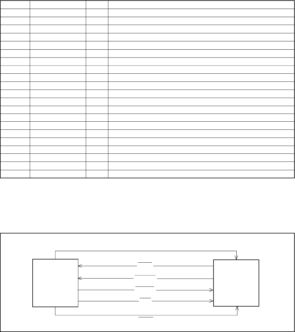
Fig. 5-1 Internal Bus Communication System
2. Internal Communication Bus
The SYA block carries out overall control of camera operation by detecting the input from the keyboard and the condition of the
camera circuits. The 8-bit microprocessor reads the signals from each sensor element as input data and outputs this data to the
camera circuits (ASIC) or to the LCD display device as operation mode setting data. Fig. 5-1 shows the internal communication
between the 8-bit microprocessor, ASIC and SPARC lite circuits.
Table 5-1. 8-bit Microprocessor Port Specification
63
64
53
-
54
GND
59
AV_JACK I AV JACK connection detection (L= connection)
VSS1
UNREG SY I Camera power voltage input
61
62
XOUT O Main clock oscillation terminal (4 MHz)
VDD1 -VDD
51 FRAME_VALID I CMOS_V signal
52 KEY_2ND I Key input 2nd SHUTTER (L= input)
55
56
RESET IMicroprocessor reset input (L= reset)
57
XCIN ISub clock oscillation terminal (32.768 kHz)
58
XCOUT O Sub clock oscillation terminal (32.768 kHz)
60
XIN I Main clock oscillation terminal (4 MHz)
8-bit
Microprocessor
ASIC
SREQ
ASIC SO
ASIC SI
SCK
MRST
43 KEY_LEFT I Key input LEFT (L= input)
49 BAT_OFF I
47
50
46
48
NOT USED
NOT USED
NOT USED
O
O
O
-
-
-
Battery OFF detection (L= battery OFF)
Serial communication request signal
SREQ I/O
44 HINJI I LCD panel rotation detection (L= panel inversion)
45 NOT USED O -
TH_TEMP ICamera temperature detection
SO O Serial data output
SI ISerial data input
PLLEN

– 10 –
ASIC,
memory CMOS 8 bit CPU
Power voltage
Power OFF
Play back
LCD finder
3.3 V 1.0 V 1.8 V 2.8 V (A)
2.8 V (D), 1.8 V (D) 3.2 V
OFF OFF 32KHz
OFF OFF 32KHz
ON ON 4 MHz
ON OFF 4 MHz
Table 5-2. Camera Mode
Note) 4 MHz = Main clock operation, 32 kHz = Sub clock operation
3. Power Supply Control
The 8-bit microprocessor controls the power supply for the overall system.
The following is a description of how the power supply is turned on and off. When the battery is attached, a regulated 3.2 V (power
off: 2.4 V) voltage is normally input to the 8-bit microprocessor (IC301) by IC302, so that clock counting and key scanning is
carried out even when the power switch is turned off, so that the camera can start up again. When the battery is removed, the 8-
bit microprocessor operates in sleep mode using the backup battery. At this time, the 8-bit microprocessor only carries out clock
counting, and waits in standby for the battery to be attached again. When a switch is operated, the 8-bit microprocessor supplies
power to the system as required.
The 8-bit microprocessor first set the P ON signal at pin (40) and the P ON2 signal at pin (41) to high, and then turns on the DC/
DC converter. After this, low signal is output from pin (17) so that the ASIC is set to the reset condition. After this these pins set
to high, and set to active condition. Once it is completed, the ASIC returns to the reset condition, all DC/DC converters are turned
off and the power supply to the whole system is halted.
Power switch ON - Auto power OFF
CAMERA

– 11 –
MEMO
– 12 –
H
D
A
EH
G
G
C
F
B
B
C
D
1
2
4
3
4
D
B
A
C
7
5
6
8
9
10
11
12
13
14
15
16
17
18
19
21
22
23
23
24
25
26
27
27
28
29
30
32
33
34
35
36 37
20
31
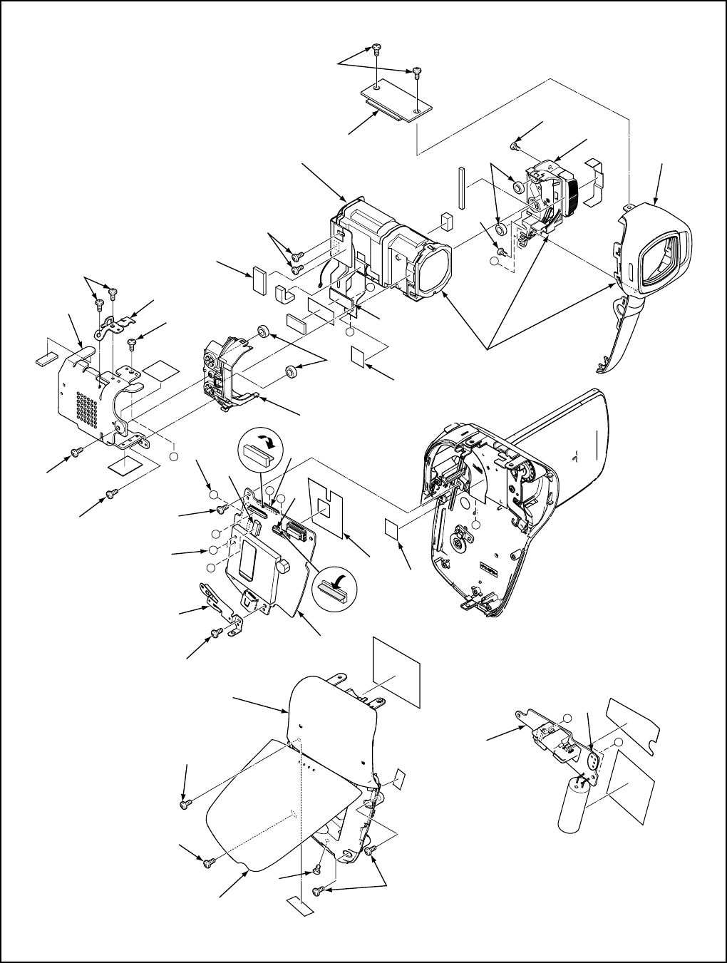
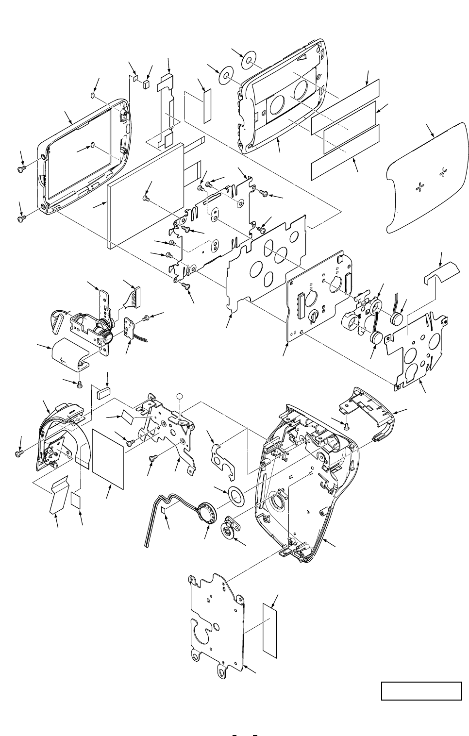
2. DISASSEMBLY
2-1. REMOVAL OF ST1 BOARD, LENS AND CP1 BOARD
NOTE: Discharge a strobe capacitor
with the discharge jig (VJ8-0188) for
electric shock prevention.
When assembling,
tighten the screws order.
A → B → C → D
– 13 –
1. Screw 1.7 x 6
2. Open the cover battery.
3. Screw 1.7 x 4.5
4. Three screws 1.7 x 6
5. Two screws 1.7 x 4.5
6. Cabinet top
7. Compl, cabi mid
8. Screw 1.7 x 3
9. Two screws 1.7 x 2
10. Holder top
11. Connector (C)
12. Remove the solder. (D)
13. ST1 board
14. Heat sink rubber left
15. Screw 1.7 x 2.5
16. Screw 1.7 x 4
17. Two screws 1.7 x 2
18. Heat sink left
19. Connector (B)
20. Spacer cp1 lens
21. FPC (H)
22. Cabinet front + assy lamp + lens
23. Two screws 1.7 x 3
24. Cabinet front
25. Assy, lamp
26. Holder lens left
27. Holder lens
28. Assy, FPC CA1 SV-SG214
29. Screw 1.7 x 3.5
30. Earth USB
31. Spacer cp1 lens
32. Screw 1.7 x 3
33. CP1 board
34. Spacer CP1
35. Remove the solder. (F)
36. Connector (E)
37. FPC (G)
7. Compl, cabi mid
10. Holder top
1122
33
13. ST1 board
22. Cabinet front + assy lamp + lens
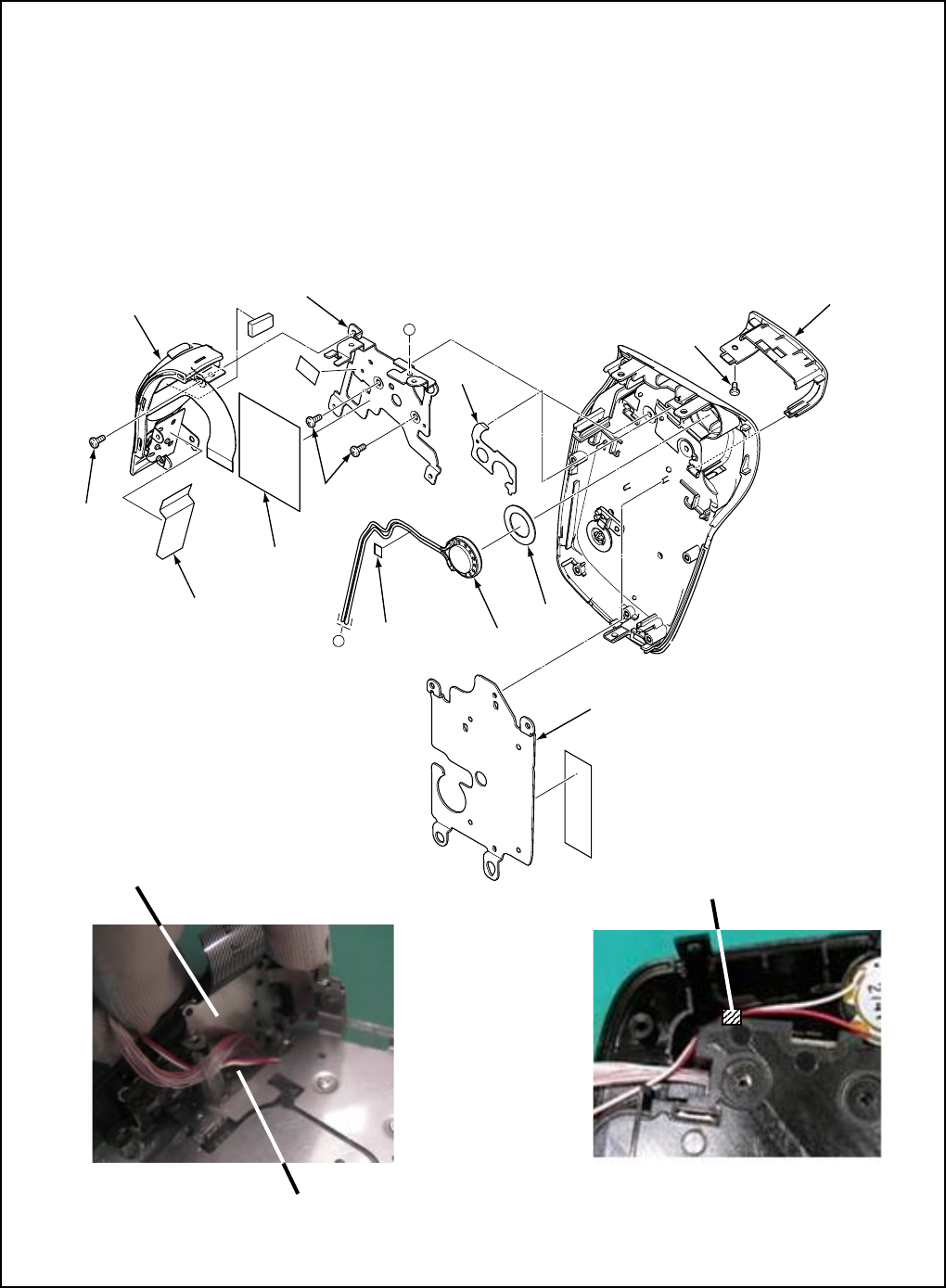
– 14 –
A
F
1
2
3
4
5
6
7
8
9
10 11
12
13
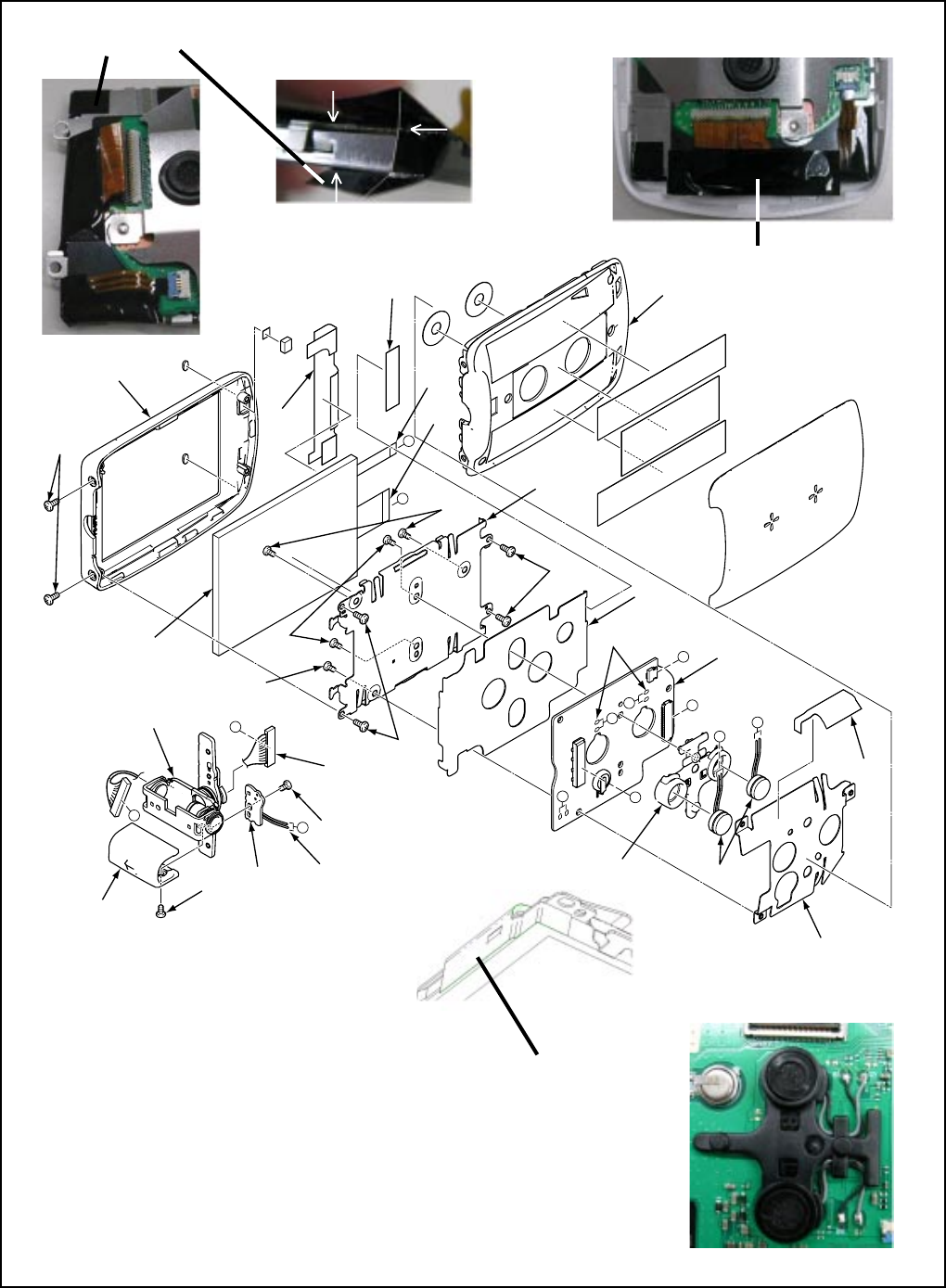
2-2. REMOVAL OF UNIT CONTROL
1. Heat sink tape joint
2. Screw 1.7 x 3.5
3. Unit, control
4. Spacer unit
5. Heat sink right
6. Screw 1.7 x 2
7. Two screws 1.7 x 2.5
8. Holder joint
9. Earth spring right
10. Spacer wire
11. Speaker, 8
12. Spacer speaker
13. Cover joint inner
Pass in the hole.
3. Unit, control 10. Spacer wire
– 15 –
I
J
K
J
K
I
E
L
N
N
M
M
L
2
1
3
4
6
7
8
9
10
12
13
14
15
16
17
17
18
22
20
21
19
23
24
11
11
25
5
15
A
C
B
D
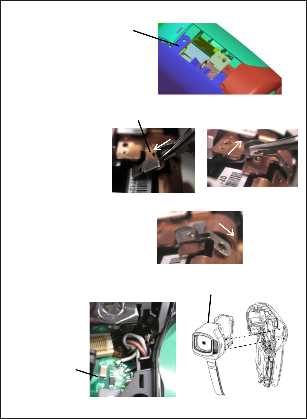
2-3. REMOVAL OF TB1 BOARD AND VF1 BOARD
1. Screw 1.7 x 2
2. Cover joint
3. Two screws 1.7 x 3
4. Cover LCD back
5. Spacer LCD C
6. Remove the solder.
7. Connector
8. Assy, joint
9. Screw 1.7 x 2
10. TB1 board
11. Four screws 1.7 x 2.5
12. Cover LCD front
13. Spacer LCD B
14. Spacer LCD A
15. Two FPCs
16. LCD
17. Three screws 1.7 x 2
18. Shield VF1
19. Remove the solder.
20. Two screws 1.7 x 3
Microphone dressing method
11
33
22
LCD side
VF1 board side
14. Spacer LCD A
21. Holder VF
22. Microphone
23. VF1 board
24. Holder monitor
25. Spacer VF
13. Spacer LCD B
5. Spacer LCD C
When assembling,
tighten the screws order.
A → B → C → D
– 16 –
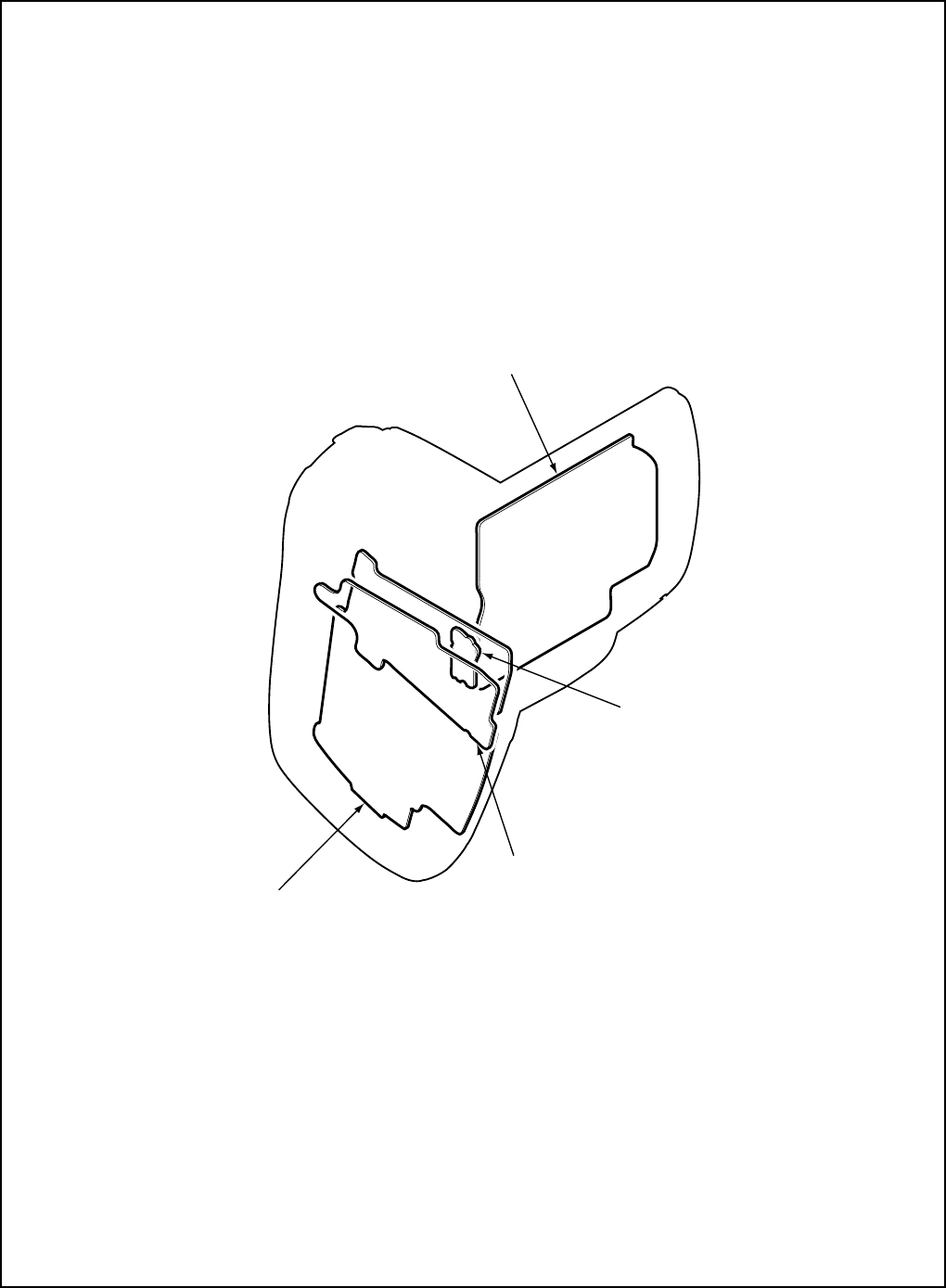
2-4. BOARD LOCATION
VF1 board
CP1 board
TB1 board
ST1 board
– 17 –
3. ELECTRICAL ADJUSTMENT
3-1. Table for Servicing Tools
Download the calibration software and the firmware
from the following URL.
http://www.digital-sanyo.com/overseas/service/
Place the DscCalDi.exe file, camapi32.dll file and
QrCodeInfo.dll file together into a folder of your
choice.
3-2. Equipment
1. PC (IBM R -compatible PC, Windows 2000 or XP or Vista)
3-3. Adjustment Items and Order
1. Lens Adjustment (Infinity)
2. Lens Adjustment (1m)
3. AWB Adjustment
4. CCD White Point Defect Detect Adjustment
5. CCD Black Point And White Point Defect Detect Adjust-
ment In Lighted
Note: If the lens, CCD and board and changing the part, it is
necessary to adjust again. Item 1-5 adjustments should be
carried out in sequence.
3-4. Setup
1. System requirements
Windows 2000 or XP or Vista
IBM R -compatible PC with pentium processor
USB port
40 MB RAM
Hard disk drive with at least 15 MB available
VGA or SVGA monitor with at least 256-color display
2. Installing USB driver
Install the USB driver with camera or connection kit for PC.
3. Pattern box
Turn on the switch and wait for 30 minutes for aging to take
place before using Color Pure. It is used after adjusting the
chroma meter (VJ8-0192) adjust color temperature to 3100 ±
20 K and luminosity to 900 ± 20 cd/m2. Be careful of handling
the lump and its circumference are high temperature during
use and after power off for a while.
4. Computer screen during adjustment
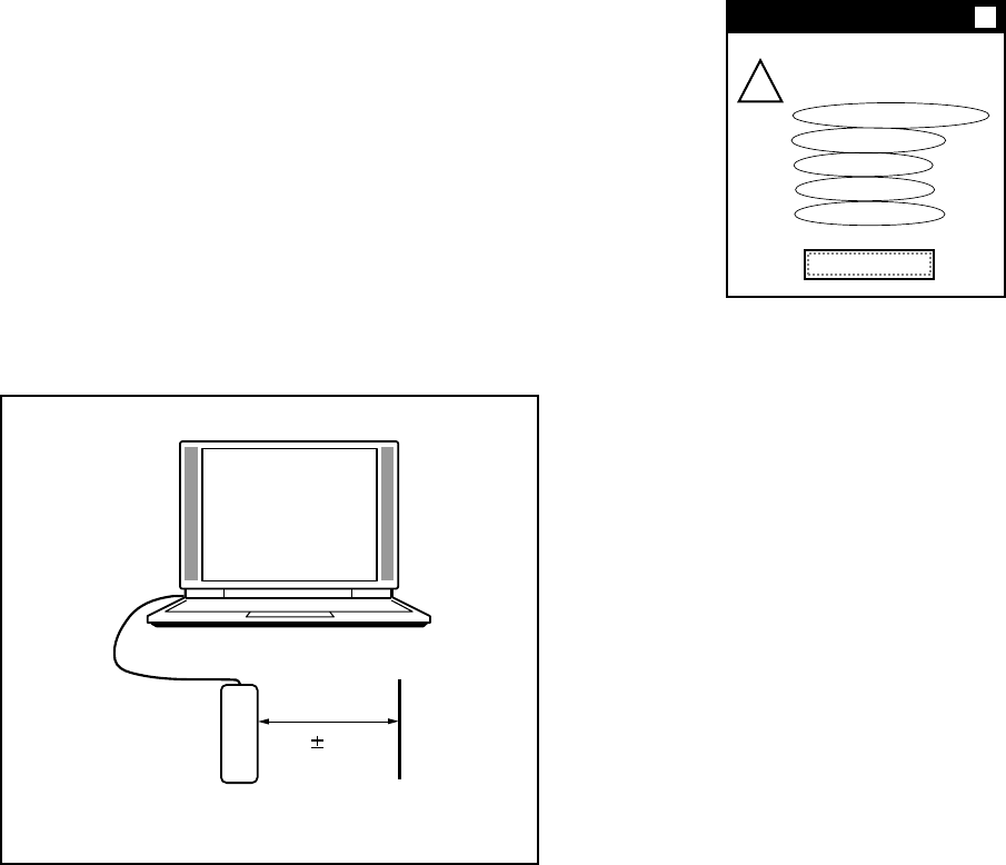
3-5. Connecting the camera to the computer
This camera requires a DC adaptor (sold separately) in order
to use an AC adaptor.
1. Insert the DC adaptor to the camera.
2. Insert the AC adaptor’s cable to DC terminal of the DC
adaptor.
3. Line up the arrow on the cable connector with the notch on
the camera's USB port. Insert the connector.
4. Locate a USB port on your computer.
5. If “USB CONNECTION” is displayed, choose the “COM
PUTER”, and press the SET button.
Next, choose the “CARD READER”, and press the SET
button.
Ref. No. Name Part code
J-1
J-2
J-3
VJ8-0190
Pattern box
Calibration software
J-4
Number
1
1
1
Chroma meter
VJ8-0192
1
Spare lump (pattern box)
VJ8-0191
J-5
J-1 J-3
J-4 J-5
1
Discharge jig
VJ8-0188
J-6 1
Collimator
VJ8-0260
J-7 1
Spare lump (collimator)
VJ8-0282
J-8 1
Siemens star chart
J-8
Firmware
Data
AWB
Focus
UV Matrix
R Bright
RGB Offset
Tint
B Bright
Gain
Phase
LCD
Calibration Upload
PAF Cal.
LCD Type H AFC Test
VCOMDC
VCOMPP
Cal Data
Cal Mode
OK
OK
EVF
USB storage
Get
Set
VID Set
PID Set
Serial Set
Rev. Set
Setting
Language
Video Mode
VCO
Factory Code
Hall Cal.
Backrush pulse :
Set
Get
– 18 –
3-8. Adjust Specifications
1. Lens Adjustment (Infinity)
Preparation:
POWER switch: ON
If using a ready-made collimator, set to infinity.
Note:
Do not vibrate during the adjustment.
The temperature of the camera should be allowed to reach
room temperature before adjusting the focus. If any slight in-
creases or decreases in room temperature occur, wait until
the temperature of the camera reaches room temperature
before carrying out adjustment.
Adjustment method:
1. Set the camera so that it becomes center of the siemens
star chart in the collimator (zoom wide and tele).
(Set a distance of 0.5-1.0 cm between camera lens and
collimator lens when zoom tele edge. Do not touch the
each lens.)
2. Double-click on the DscCalDi.exe.
3. Select “Infinity Cal.” on the LCD “Test”, and click the “Yes”.
4. Lens infinity adjustment value will appear on the screen.
5. Click the OK.
2. Lens Adjustment (1m) is carried out after this adjust-
ment.
3-6. The adjustment item which in necessary in part exchange
Camera
Collimator
COMPL PWB CP-1
Factory
Cord
Setting
Language
Setting
COMPL PWB VF-1
COMPL PWB ST-1
COMPL PWB TB-1
Reset
Setting
LENS
Lens
Adjust-
ment
(1 m)
AWB
Adjust-
ment
USB
storage
information
registration
CCD White
Point
Defect
Detect
Adjustment
CCD Black
Point And
White Point
Defect Detect
Adjustment
In Lighted
: Be sure to carry out the necessary adjustments after replacing the unit.
: Adjustment is possible from the menu setting screen of the camera and by using the calibration software.
Lens
Adjust-
ment
(Infinity)
ASSY, FLEXIBLE PWB COMP3
Dsc Calibration x
OK
Infinity calibration :
AF_TEMP_AD_I: 329
PZ_BR: 8
AF_BR: 6
AF_I_WIDE: -16
AF_I_MID1: -18
AF_I_MID2: 2
AF_I_TELE: 49
IRIS_GAIN: 62
IRIS_OFFSET: 107
Copy
3-7. Updating the firmware
Check the firmware version immediately after the CP1 board has been replaced. If an old version is being used, interfer-
ence and errors in operation may also occur. If an old version is being used, update it with a newer version.
Refer to 3-13. Firmware uploading procedure. (Page 21)
– 19 –
Adjustment value determination is effectuated using below val-
ues.
The adjustment values fulfill the conditions below, they are de-
termined as within specifications.
Adjustment value determination
AF_TEMP_AD_I: ATADI
ATADI: adjustment value of focus temperature A/D
(0<ATADI<1023)
PZ_BR: PBR
PBR: adjustment value of zoom backrush pulse
(0<=PBR<=10)
AF_BR: ABR
ABR: adjustment value of focus backrush pulse
(0<=ABR<=10)
AF_I_WIDE: ZIW
ZIW: infinity adjustment value of focus at zoom position
wide (-40<=ZIW<=40)
AF_I_MID1: ZIM1
ZIM1: infinity adjustment value of focus at zoom position
middle1 (-70<=ZIM1<=70)
AF_I_MID2: ZIM2
ZIM2: infinity adjustment value of focus at zoom position
middle2 (-58<=ZIM2<=82)
AF_I_TELE: ZIT
ZIT: infinity adjustment value of focus at zoom position tele
(-41<=ZIT<=99)
IRIS_GAIN: g
g: adjustment value of gain (0<=g<=255)
IRIS_OFFSET: o
o: adjustment value of offset (0<=o<=255)
2. Lens Adjustment (1m)
Preparation:
POWER switch: ON
Adjustment condition:
Siemens star chart (A3)
Fluorescent light illumination with no flicker (incandescent light
cannot be used.)
Illumination above the subject should be 700 lux ± 10%.
Note:
Do not vibrate during the adjustment.
The temperature of the camera should be allowed to reach
room temperature before adjusting the focus. If any slight in-
creases or decreases in room temperature occur, wait until
the temperature of the camera reaches room temperature
before carrying out adjustment.
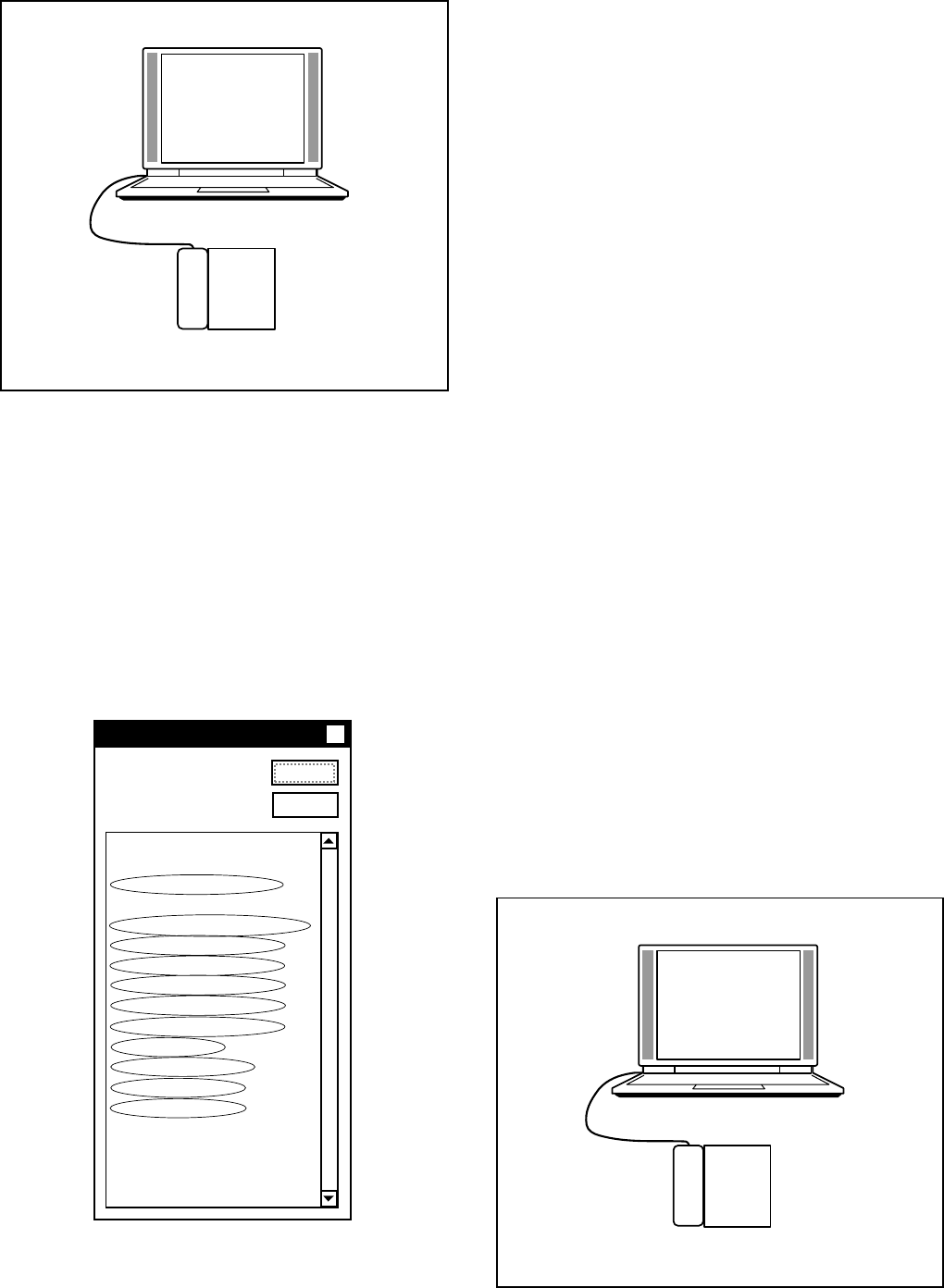
Adjustment method:
1. Set the siemens star chart 100 ± 0.5 cm from lens surface
(zoom wide position) so that it becomes center of the
screen (zoom wide and tele). Set the camera and the chart
in a straight, and do not put optical systems (mirror and
conversion lens etc.)
2. Double-click on the DscCalDi.exe.
3. Click the “Focus”, and Click the “Yes”.
4. Lens adjustment value will appear on the screen.
5. Click the OK.
Adjustment value determination is effectuated using below val-
ues.
The adjustment values fulfill the conditions below, they are de-
termined as within specifications.
Adjustment value determination
AF_TEMP_AD: ATAD
ATAD: adjustment value of focus temperature A/D
(0<ATAD<1023)
AF_WIDE: ZW
ZW: adjustment value of focus at zoom position wide
(–50<=ZW<=50)
AF_MID1: ZM1
ZM1: adjustment value of focus at zoom position middle1
(–80<=ZM1<=80)
AF_MID2: ZM2
ZM2: adjustment value of focus at zoom position middle2
(–68<=ZM2<=92)
AF_TELE: ZT
ZT: adjustment value of focus at zoom position tele
(–51<=ZT<=109)
Camera
(zoom wide) 100 0.5 cm
Siemens
star chart
DscCalDi x
OK
Focus Result
AF_TEMP_AD: 484
AF_WIDE: -15
AF_MID1: 12
AF_MID2: 48
AF_TELE: 163
!
– 20 –
3. AWB Adjustment
Preparation:
POWER switch: ON
Setting of pattern box:
Color temperature: 3100 ± 20 (K)
Luminance: 900 ± 20 (cd/m2)
Adjusting method:
1. When setting the camera in place, set it to an angle so that
nothing appears in any part of the color viewer except the
white section. (Do not enter any light.)
2. Double-click on the DscCalDi.exe.
3. Click the AWB, and click the Yes.
4. AWB adjustment value will appear on the screen.
5. Click the OK.
Adjustment value determination is effectuated using the
“CHECK", “CHECK_ND”, "MS", “MS_M”, “MS_C”, “MS_C2”,
“IRIS_PWM1”, “IRIS_PWM2”, “IRIS_PWM3”, “IRIS_PWM4”
and “IRIS_PWM5” values. If
CHECK= wc0, wc1, wc2
CHECK_ND= wnc0, wnc1, wnc2
MS= ms1, ms2,
MS_M= ms3, ms4,
MS_C= ms5, ms6,
MS_C2= ms7, ms8,
IRIS_PWM1= s1, s2
IRIS_PWM2= s3, s4
IRIS_PWM3= s5, s6
IRIS_PWM4= s7, s8
IRIS_PWM5= s9, s10
the adjustment values fulfill the conditions below, they are de-
termined as within specifications.
Adjustment value determination
wc0=128 ± 2, wc1=128 ± 2, wc2=130 ± 40
wnc0=128 ± 2, wnc1=128 ± 2, wnc2=130 ± 40
1200<=ms1<=4450, 240<=ms2<=2240, 980<=ms3<=2980,
820<=ms4<=2820, 700<=ms5<=2700, 570<=ms6<=2570,
470<=ms7<=2470, 360<=ms8<=2360
0<=s1<=255, 0<=s2<=255, 0<=s3<=255, 0<=s4<=255,
0<=s5<=255, 0<=s6<=255, 0<=s7<=255, 0<=s8<=255,
0<=s9<=255, 0<=s10<=255
ms2<ms8<ms7<ms6<ms5<ms4<ms3<ms1
s1>s2>s3>s4>s5>s6>s7>s8>s9>s10
Adjustment values other than the above are irrelevant.
4. CCD White Point Defect Detect Adjustment
Preparation:
POWER switch: ON
Adjustment method:
1. Double-click on the DscCalDi.exe.
2. Select “CCD Defect” on the LCD “Test”, and click the “Yes”.
3. After the adjustment is completed, OK will display.
4. Click the OK.
5. CCD Black Point And White Point Defect Detect
Adjustment In Lighted
Camera
Pattern box
Camera
Pattern box
Dsc Calibration
x
OK
AWB Results:
1:
WB=242,494,415
CHECK=128,128,115
WB_ND=239,493,412
CHECK_ND=128,128,112
IRIS_PWM1=221, 210
IRIS_PWM2=201,194
IRIS_PWM3=188,183
IRIS_PWM4=179,175
IRIS_PWM5=165,157
MS=1602,793
MS_M=1321,1165
MS_C=1065,968
MS_C2=890,846
Fno_FOR_ISO=80
SS_FOR_ISO=-1
YLEVEL_FOR_ISO=-1
Copy
– 21 –
3-13. Firmware uploading procedure
1. Uploading the firmware should be carried out if the version
number (COMPL PWB XX-X) on the replacement circuit
board is lower than the version of the distributed firmware.
For XX-X, enter the name of the circuit board containing the
firmware.
2. The firmware is distributed by e-mail in self-extracting archive
format. Change the extension of the distributed file to .EXE
and save it in your preferred folder.
3. When you double-click the saved file, the firmware (binary
file) will be saved in the same folder.
4. The firmware must not be distributed without permission.
1. Overwriting firmware from the SD card
Preparation:
SD card: SD card with firmware rewritten into the root direc-
tory
Data: S214Nxxx.BIN (xxx: version)
Overwriting method:
1. Insert the above SD card.
2. Turn on the camera.
3. Set the REC/PLAY switch to the PLAY.
4. Press the MENU button.
5. Choose the Option menu.
6. Choose the FORMAT.
7. Toggle the SET button to the left for 2 seconds. FIRMWARE
UPDATE will display.
8. Choose YES.
9. Press the SET button. Update is starting.
Note:
Do not turn off the camera’s power or remove the SD card
while the firmware is being updated.
The power will turn on automatically after the update is com-
plete.
2. Overwriting firmware from the calibration software
Preparation:
PC with overwriting firmware copied to the preferred folder in
the HD.
Data: S214Nxxx.BIN (xxx: version)
Overwriting method:
1. Connect the camera’s USB/AV terminal to the computer’
USB connector.
2. The USB Connection screen appears on the camera’s LCD
monitor. Choose the “COMPUTER”, and press the SET
button. Next, choose the “CARD READER”, and press the
SET button.
3. Double-click on the DscCalDi.exe.
4. Click the Firmware.
5. Choose the fimware file to use for overwriting, and click
the Yes.
6. Update is starting. The message will appear, and choose
OK.
7. After the update is complete, disconnect the USB cable
and turn the camera’s power off.
Note:
Do not turn off the camera’s power while the firmware is be-
ing updated.
3-9. Factory Code Setting
1. Check the "Factory Code" display within the Setting group.
2. For U.S.A., Canada and NTSC general area
If "FC_SANYO_U" does not appear, click on the " " mark
located on the right of the "Factory Code" display BOX and
select "FC_SANYO_U".
3. For Europe and PAL general area
If "FC_SANYO_EX" does not appear, click on the " " mark
located on the right of the "Factory Code" display BOX and
select "FC_SANYO_EX".
3-10. Language Setting
1. Click on the " " mark located on the right of the
"Language" display BOX.
2. Select language. (Default is English.)
3. End "DscCal" and remove the camera before turning the
camera power OFF.
3-11. Reset Setting
Carry out reset settings after replacing CP1 board.
1. Turn on the camera.
2. Press the MENU button.
3. Choose the Option menu.
4. Choose the RESET SETTINGS, and press the SET button.
5. Select RESET, and press the SET button.
3-12. The Compulsive boot starting method
1. Keep MENU button, SET button, and SHUTTER button de-
pressed while switching on the power.
2. Connect the camera and the computer with USB cable.
Firmware
Data
AWB
Focus
UV Matrix
R Bright
RGB Offset
Tint
B Bright
Gain
Phase
LCD
Calibration Upload
PAF Cal.
LCD Type H AFC Test
VCOMDC
VCOMPP
Cal Data
Cal Mode
OK
OK
EVF
USB storage
Get
Set
VID Set
PID Set
Serial Set
Rev. Set
Setting
Language
Video Mode
VCO
Factory Code
Hall Cal.
Backrush pulse :
Set
Get
Preparation:
POWER switch: ON
Setting of pattern box:
Color temperature: 3100 ± 20 (K)
Luminance: 900 ± 20 (cd/m2)
Adjusting method:
1. Set the camera 0 cm from the pattern box. (Do not enter
any light.)
2. Double-click on the DscCalDi.exe.
3. Select “CCD Black” on the LCD “Test”, and click the “Ye s ”.
4. After the adjustment is completed, the number of defect
will appear.
5. Click the OK.
– 22 –
4. USB STORAGE INFORMATION
REGISTRATION
USB storage data is important for when the camera is con-
nected to a computer via a USB connection.
If there are any errors in the USB storage data, or if it has not
been saved, the USB specification conditions will not be sat-
isfied, so always check and save the USB storage data.
Preparation:
POWER switch: ON
Adjustment method:
1. Connect the camera to a computer. (Refer to 3-5. Con-
necting the camera to the computer on the page 17.)
2. Double-click on the DscCalDi.exe.
3. Click on the Get button in the USB storage window and
check the USB storage data.
VID: SANYO
PID: CG9
Serial:
Rev. : 1.00
4. Check the “Serial” in the above USB storage data. If the
displayed value is different from the serial number printed
on the base of the camera, enter the number on the base
of the camera. Then click the Set button.
5. Next, check VID, PID and Rev. entries in the USB storage
data. If any of them are different from the values in 3. above,
make the changes and then click the corresponding Set
button.
Firmware
Data
AWB
Focus
UV Matrix
R Bright
RGB Offset
Tint
B Bright
Gain
Phase
LCD
Calibration Upload
PAF Cal.
LCD Type H AFC Test
VCOMDC
VCOMPP
Cal Data
Cal Mode
OK
OK
EVF
USB storage
Get
Set
VID Set
PID Set
Serial Set
Rev. Set
Setting
Language
Video Mode
VCO
Factory Code
Hall Cal.
Backrush pulse :
Set
Get
– 23 –
5. TROUBLESHOOTING GUIDE
POWER LOSS INOPERTIVE
PUSH THE POWER
SW FOR A WHILE
IC301-14
KEY_POWER INPUT CHECK POWER SW
IC301-9, 36, 59
(VDD)
IC301-53
(RESET)
CHECK IC302
CHECK IC302
IC301-49
(BAT OFF) CHECK IC302
IC301-55
OSCILLATION CHECK X3002
CHECK IC301
PUSH SHUTTER
BUTTON
IC301-24, 52
KEY INPUT CHECK UNIT SW
IC501-D5, F6 (PON)
Q5005-2 (PON2)
Q5004-1 (PAON1)
IC503-4(PAON2)
CHECK IC101, IC301,
PWA BLOCK,
CAA BLOCK
SERIAL
COMMUNICATION
CHECK IC301,
CP1 DMA BLOCK
CHECK CP1 DMA
BLOCK
TAKING INOPERATIVE
HIGH
LOW
LOW
LOW
NO
LOW
HIGH
HIGH
HIGH
YES
YES
HIGH
OK
NO
LOW
NG
NO PICTURE
MAIN CLOCK FOR SYSTEM OPERATION
NO OPERATION IF ABSENT
CHECK X1102 OSCILLATOR
IC101-AK20 (XOUT)
CHECK
OSCILLATION
IC301-63, 64
(ASIC_SO, ASIC_SI)
CHECK SOLDERING
OF MEMORY
EACH PIN
INCORRECT HANDSHAKING
BETWEEN 8-BIT CPU AND ASIC
CHECK EACH INTERFACE
OK
OK
NG
NG

24
6. PARTS LIST
ACCESSORIESPACKING MATERIALS
LOCATION PARTS NO. DESCRIPTION LOCATION PARTS NO. DESCRIPTION
Note: Please refer to the table of next page for the accessories.
7001 636 115 5564 CARTON INNER-SG214/U,VPC-CG9BK,VPC-CG9
7001 636 115 5571 CARTON INNER-SG214/EX,VPC-CG9EXBK,
VPC-CG9GXBK,VPC-CG9EXW,VPC-CG9GXW,
VPC-CG9EX,VPC-CG9GXP,VPC-CG9EXP
7002 636 078 4659 CUSHION SHEET-SX792/KRNK
7003 636 099 3020 LABEL CARTON SILVER-817U2
VPC-CG9EX,VPC-CG9
7003 636 086 5068 LABEL CARTON WHITE-719EX3
VPC-CG9EXW,VPC-CG9GXW
7003 636 074 6589 LABEL CARTON PINK 712EX3
VPC-CG9GXP,VPC-CG9EXP
7004 636 114 4926 LABEL SILVER MODEL-214/EX4
VPC-CG9EX,VPC-CG9
7004 636 114 0980 LABEL WHITE MODEL-214/EX2
VPC-CG9EXW,VPC-CG9GXW
7004 636 114 4872 LABEL PINK MODEL-214/GX5
VPC-CG9GXP,VPC-CG9EXP
7005 636 115 5618 REINFORCE PAD,A-SG214/J (INNER BOTTOM)
1 636 103 1783 STRAP CAP LENS-SG112/J
2 636 113 1100 CAP LENS-SG214/J
VPC-CG9BK,VPC-CG9EXBK,VPC-CG9GXBK,
VPC-CG9EX,VPC-CG9
2 636 114 1420 CAP LENS-SG214/J2
VPC-CG9EXW,VPC-CG9GXW,VPC-CG9GXP,
VPC-CG9EXP
3 645 087 1818 CABLE,DSC USB (Dedicated USB interface cable)
4 645 087 1825 CABLE,DSC A/V (Dedicated AV interface cable)
5 645 083 6794 CORD,POWER-1.9MK,VPC-CG9BK,VPC-CG9
5 645 083 6787 CORD,POWER-1.2MK,
EXCEPTVPC-CG9BK,VPC-CG9
6 645 089 5081 BATTERY CHARGER
OR 645 093 9617 BATTERY CHARGER
7 645 089 8990 BATTERY,RECHARGE,LI-ION
8 636 113 9069 DISC,CD-ROM INST G214
VPC-CG9GXBK,VPC-CG9GXW,VPC-CG9GXP
PDF of instruction manual: English, German, French,
Spanish, Italian, Dutch, Russian, Portuguese,
Simplefied Chinese, Traditional Chinese, Korean
9053 636 114 1710 INSTRUCTION MANUAL CAMERA/SOFTWEAR
25
Table of accessories
1
1
3
3
45
5
6
6
7
7
2
8

26
CABINET AND CHASSIS PARTS 1
LOCATION PARTS NO. DESCRIPTION LOCATION PARTS NO. DESCRIPTION
1 636 114 1574 COMPL,COVER BATT-SG214
VPC-CG9BK,VPC-CG9EXBK,VPC-CG9GXBK
1 636 114 1598 COMPL,COVER BATT-SG214
VPC-CG9EXW,VPC-CG9GXW
1 636 114 4902 COMPL,COVER BATT-SG214
VPC-CG9EX,VPC-CG9
1 636 114 4919 COMPL,COVER BATT-SG214
VPC-CG9GXP,VPC-CG9EXP
2 636 113 7034 SPACER CABI MID B-SG214/J
3 636 114 4803 CABINET LEFT-SG214/EX4,VPC-CG9EX,VPC-CG9
3 636 114 4810 CABINET LEFT-SG214/GX5
VPC-CG9GXP,VPC-CG9EXP
3 636 113 0448 CABINET LEFT-SG214/J
VPC-CG9BK,VPC-CG9EXBK,VPC-CG9GXBK
3 636 114 1277 CABINET LEFT-SG214/J2
VPC-CG9EXW,VPC-CG9GXW
4 636 115 9623 HEAT SINK TAPE JOINT-214
5 636 113 0592 COVER CARD-SG214/J
VPC-CG9BK,VPC-CG9EXBK,VPC-CG9GXBK,
VPC-CG9EX,VPC-CG9
5 636 114 1260 COVER CARD-SG214/J3
VPC-CG9EXW,VPC-CG9GXW,VPC-CG9GXP,
VPC-CG9EXP
6 636 113 0639 STAND-SG214/J
VPC-CG9BK,VPC-CG9EXBK,VPC-CG9GXBK,
VPC-CG9EX,VPC-CG9
6 636 114 1291 STAND-SG214/J2
VPC-CG9EXW,VPC-CG9GXW,VPC-CG9GXP,
VPC-CG9EXP
7 636 116 0704 SPACER CABI MID-SG214/J
8 636 113 0455 CABINET MIDDLE-SG214/J
VPC-CG9BK,VPC-CG9EXBK,VPC-CG9GXBK,
VPC-CG9EX,VPC-CG9
8 636 114 1215 CABINET MIDDLE-SG214/J3
VPC-CG9EXW,VPC-CG9GXW,VPC-CG9GXP,
VPC-CG9EXP
9 636 112 4768 COMPL PWB,ST-1
10 636 109 2951 SPACER MAIN CON-SG212/J
11 636 113 0981 SPACER CP1 ST-SG214/J
12 636 113 0837 EARTH USB-SG214/J
13 636 114 1451 COMPL PWB,CP-1 F/W
14 636 114 7064 SPACER CP1-SG214/J
15 636 116 0278 SPACER HEAT SINK B-SG214
16 636 113 0905 HEAT SINK LEFT-SG214/J
17 636 114 0508 SPACER LENS TOP-SG214
18 636 113 0813 HOLDER TOP-SG214/J
19 636 113 0998 SPACER HEAT SINK-SG214/J
20 636 113 0721 HOLDER LENS LEFT-SG214/J
21 636 113 0752 HOLDER LENS-SG214/J
22 636 114 0911 ASSY,FPC CA1 SV-SG214
23 636 114 0492 SPACER LENS LEFT-SG214
24 636 114 8580 SPACER CA1-SG214/J
25 636 114 1109 SPACER CA1 CN-SG214/J
26 636 115 9661 HEAT SINK RUBBER LEFT-214
27 636 114 0461 SPACER LENS RIGHT-SG214
28 636 113 0462 CABINET TOP-SG214/J
VPC-CG9BK,VPC-CG9EXBK,VPC-CG9GXBK,
VPC-CG9EX,VPC-CG9
28 636 114 1314 CABINET TOP-SG214/J3
VPC-CG9EXW,VPC-CG9GXW,VPC-CG9GXP,
VPC-CG9EXP
29 636 115 5472 SPACER LENS-SG214/J
30 645 096 4305 ASSY,LAMP-SG214
VPC-CG9BK,VPC-CG9EXBK,VPC-CG9GXBK,
VPC-CG9EX,VPC-CG9
30 645 096 8846 ASSY,LAMP-SG214/J2
VPC-CG9EXW,VPC-CG9GXW,VPC-CG9GXP,
VPC-CG9EXP
31 636 114 1673 SPACER FLASH-SG214/J
32 636 114 1499 COMPL,CABI FRONT-SG214/J
VPC-CG9BK,VPC-CG9EXBK,VPC-CG9GXBK,
VPC-CG9EX,VPC-CG9
32 636 114 6586 COMPL,CABI FRONT-SG214/J
VPC-CG9EXP,VPC-CG9GXP
32 636 114 6579 COMPL,CABI FRONT-SG214/J
VPC-CG9EXW,VPC-CG9GXW
33 636 116 9943 SPACER CP1 LENS-SG214/J
101 411 192 4408 SCR S-TPG PAN PCS 1.7X6.0
VPC-CG9BK,VPC-CG9EXBK,VPC-CG9GXBK,
VPC-CG9EX,VPC-CG9
101 411 180 1808 SCR S-TPG PAN PCS 1.7X6.0
VPC-CG9EXW,VPC-CG9GXW,VPC-CG9GXP,
VPC-CG9EXP
102 411 192 4408 SCR S-TPG PAN PCS 1.7X6.0
VPC-CG9BK,VPC-CG9EXBK,VPC-CG9GXBK,
VPC-CG9EX,VPC-CG9
102 411 180 1808 SCR S-TPG PAN PCS 1.7X6.0
VPC-CG9EXW,VPC-CG9GXW,VPC-CG9GXP,
VPC-CG9EXP
103 411 177 0906 SCR S-TPG PAN PCS 1.7X3.5
104 411 178 9403 SCR S-TPG PAN PCS 1.7X4.0
105 411 175 5705 SCR PAN PCS 1.7X3
106 411 178 6204 SCR PAN PCS 1.7X4
107 312 060 9504 SPECIAL SCREW-1.7X2.5
108 411 199 0700 SCR TIN 1.7X2
109 411 184 0005 SCR PAN PCS 1.7X2.0
110 411 177 9503 SCR S-TPG PAN PCS 1.7X3
111 411 192 4309 SCR S-TPG PAN PCS 1.7X4.5
VPC-CG9BK,VPC-CG9EXBK,VPC-CG9GXBK,
VPC-CG9EX,VPC-CG9
111 411 207 7806 SCR S-TPG PAN PCS 1.7X4.5
VPC-CG9EXW,VPC-CG9GXW,VPC-CG9GXP,
VPC-CG9EXP
112 411 194 8305 SCR PAN PCS 1.7X4.5
VPC-CG9BK,VPC-CG9EXBK,VPC-CG9GXBK,
VPC-CG9EX,VPC-CG9
112 411 182 4609 SCR PAN PCS 1.7X4.5
VPC-CG9EXW,VPC-CG9GXW,VPC-CG9GXP,
VPC-CG9EXP
27
CABINET AND CHASSIS PARTS 1
Cabinet 1
SG214/J PARTS LIST 1
A
11
10
103
12 13
14
105
106
15
107
16
17
32
31
30
21
21
29
27
110
112
112
110
9
101
101
102
111
1
2
101
104
104
104
104
7
8
6
5
34
18
26
21
23
108
108 109
105
19
20
21
22
24
25
109
28
33

28
CABINET AND CHASSIS PARTS 2
LOCATION PARTS NO. DESCRIPTION LOCATION PARTS NO. DESCRIPTION
1 636 113 0851 HEAT SINK RIGHT-SG214/J
2 636 115 9630 HEAT SINK TAPE RIGHT-214
3 636 116 7574 ASSY,CABI RIGHT SV-214/J
VPC-CG9BK,VPC-CG9EXBK,VPC-CG9GXBK
3 636 116 7581 ASSY,CABI RIGHT SV-214/J2
VPC-CG9EXW,VPC-CG9GXW
3 636 116 7604 ASSY,CABI RIGHT SV-214/EX4
VPC-CG9,VPC-CG9EX
3 636 116 7611 ASSY,CABI RIGHT SV-214/GX5
VPC-CG9EXP,VPC-CG9GXP
4 636 113 0424 BUTTON POWER-SG214/J
VPC-CG9BK,VPC-CG9EXBK,VPC-CG9EX,
VPC-CG9
4 636 114 1178 BUTTON POWER-SG214/J2
VPC-CG9EXW,VPC-CG9GXW,VPC-CG9GXP,
VPC-CG9EXP
5 636 114 1116 SPACER SPEAKER-SG214/J
6 645 093 3424 SPEAKER,8
7 636 114 1536 SPACER WIRE-SG214/J
8 636 113 7331 EARTH SPRING RIGHT-SG214
9 636 113 0783 HOLDER JOINT-SG214/J
10 636 113 9656 SPACER JOINT BASE-SG214/J
11 636 115 9623 HEAT SINK TAPE JOINT-214
12 636 114 1093 SPACER UNIT-SG214/J
13 645 096 2851 UNIT,CONTROL-SG214/J
VPC-CG9BK,VPC-CG9EXBK,VPC-CG9GXBK,
VPC-CG9EX,VPC-CG9
13 645 096 8150 UNIT,CONTROL-SG214/J3
VPC-CG9EXW,VPC-CG9GXW,VPC-CG9GXP,
VPC-CG9EXP
14 636 113 0530 COVER JOINT -SG214/J
15 636 105 1545 ASSY,JOINT-SG211/J
16 636 106 6310 ASSY,SHIELD WIRE CP1-VF1
17 636 112 7592 COMPL PWB,TB-1
18 636 113 0509 COVER JOINT INNER-SG214/J
19 636 113 0943 SHIELD VF1-SG214/J
20 636 114 7521 SPACER LCD B-SG214/J
21 645 095 9943 MICROPHONE
22 636 113 0622 HOLDER VF-SG214/J
23 636 112 4775 COMPL PWB,VF-1
24 636 116 5976 SPACER VF-SG214/J
25 636 113 0806 HOLDER MONITOR-SG214/J
26 645 095 7642 LCD(TX06D107TM0AAA)
27 636 114 4629 COVER LCD FRONT-SG214/EX4
VPC-CG9EX,VPC-CG9
27 636 114 4636 COVER LCD FRONT-SG214/GX5
VPC-CG9GXP,VPC-CG9EXP
27 636 113 0646 COVER LCD FRONT-SG214/J
VPC-CG9BK,VPC-CG9EXBK,VPC-CG9GXBK
27 636 114 1369 COVER LCD FRONT-SG214/J2
VPC-CG9EXW,VPC-CG9GXW
28 636 099 6991 COVER STAND-SG111/J
VPC-CG9BK,VPC-CG9EXBK,VPC-CG9GXBK,
VPC-CG9EX,VPC-CG9
28 636 114 1413 COVER STAND-SG214/J2
VPC-CG9EXW,VPC-CG9GXW,VPC-CG9GXP,
VPC-CG9EXP
29 636 115 4772 ADHESIVE MAGNET-SG214/J
30 645 096 8129 MAGNET-SG214/J
31 636 115 4789 SPACER LCD A-SG214/J
32 636 114 6715 SPACER LCD C-SG214/J
33 636 113 0653 COVER LCD BACK-SG214/J
VPC-CG9BK,VPC-CG9EXBK,VPC-CG9GXBK,
VPC-CG9EX,VPC-CG9
33 636 114 1383 COVER LCD BACK-SG214/J2
VPC-CG9EXW,VPC-CG9GXW,VPC-CG9GXP,
VPC-CG9EXP
34 636 114 1079 ADHESIVE LCD BACK-SG214/J
35 636 109 3071 SPACER MIC FILTER-SG212/J
VPC-CG9BK,VPC-CG9EXBK,VPC-CG9GXBK,
VPC-CG9EX,VPC-CG9
35 636 115 5311 SPACER MIC FILTR-SG214/J2
VPC-CG9EXW,VPC-CG9GXW,VPC-CG9GXP,
VPC-CG9EXP
36 636 113 0974 SPACER MIC-SG214/J
37 636 114 4643 DEC LCD BACK-SG214/EX4
VPC-CG9EX,VPC-CG9
37 636 114 4650 DEC LCD BACK-SG214/GX5
VPC-CG9GXP,VPC-CG9EXP
37 636 113 0691 DEC LCD BACK-SG214/J
VPC-CG9BK,VPC-CG9EXBK,VPC-CG9GXBK
37 636 114 1390 DEC LCD BACK-SG214/J2
VPC-CG9EXW,VPC-CG9GXW
38 636 116 9943 SPACER CP1 LENS-SG214/J
39 636 114 0492 SPACER LENS LEFT-SG214
103 411 177 0906 SCR S-TPG PAN PCS 1.7X3.5
108 411 199 0700 SCR TIN 1.7X2
109 411 184 0005 SCR PAN PCS 1.7X2.0
113 411 177 8100 SCR S-TPG PAN PCS 1.7X2.5
114 312 060 7906 SPECIAL SCREW-1.7X3.0
115 411 199 0809 SCR TIN 1.7X3
VPC-CG9BK,VPC-CG9EXBK,VPC-CG9GXBK,
VPC-CG9EX,VPC-CG9
115 411 199 0908 SCR TIN 1.7X3
VPC-CG9EXW,VPC-CG9GXW,VPC-CG9GXP,
VPC-CG9EXP
116 411 176 1003 SCR PAN PCS 1.7X2.5
29
CABINET AND CHASSIS PARTS 2
Cabinet 2
SG214/J PARTS LIST 2
A
2
1
3
4
6
9
11
116
116
103
10
7
12
13
16
108 108
15
36
36
32
14
108
18
108
5
8
17
109 113
108
114
114 25
113
113
113
34
34
35
37
20
21
21
19
23
24
22
33
31
29 30
28
27
28
26
115
115
39
38

30
Note:
1. Materials of Capacitors and Resistors are abbreviated as follows ;
Resistors Capacitors
MT-FILM Metallized Film Resistor MT-POLYEST Metallized Polyester Capacitor
MT-GLAZE Metallized Glaze Resistor MT-COMPO Metallized Composite Capacitor
OXIDE-MT Oxide Metallized Film Resistor TA-SOLID Tantalum Solid Capacitor
AL-SOLID Aluminum Solid Capacitor
NP-ELECT Non-Polarized Electrolytic Capacitor
OS-SOLID Aluminum Solid Capacitors with Organic
Semiconductive Electrolytic Capacitor
DL-ELECT Double Layered Electrolytic Capacitor
POS-SOLID Polymerized Organic Semiconductor Capacitor
2. Tolerance of Capacitor (10pF over) and Resistor are noted with follow symboles.
F ............1% G ............2% J ............5% K ............10%
M ..........20% N ..........30% Z ..........+80% ~ -20%
3. Capacitors
U : µF P : pF
4. Inductors
UH : µH MH : mH
5. N.S.P. : Not available as service parts.
ELECTRICAL PARTS
LOCATION PARTS NO. DESCRIPTION LOCATION PARTS NO. DESCRIPTION
COMPL PWB,CP-1 F/W
636 114 1451
(SEMICONDUCTORS)
Q1301 305 168 3703 TR DTC144EM
OR 305 216 1200 TR RN1104MFV
OR 305 172 4703 TR UNR32A3
Q1302 405 218 3902 TR UP0431300
OR 305 167 0406 TR EMD12
Q1403 405 218 3902 TR UP0431300
OR 305 167 0406 TR EMD12
Q3001 305 173 4405 TR DTC114TM
OR 305 173 7406 TR UNR32A5
Q3002 305 210 5709 TR UP0KG8D
OR 305 217 3906 TR HN2E07JE
OR 305 200 9007 TR EML17
Q3003 305 183 7700 TR EMH10
Q3004 305 168 4007 TR DTA114EM
OR 305 216 1408 TR RN2102MFV
OR 305 172 4802 TR UNR31A1
Q5003 405 218 4701 TR SSM3J120TU
Q5004 305 181 4909 TR 2SK3541
Q5005 305 184 6009 TR UP03396
Q5007 405 219 2706 TR MCH5835-E
Q5008 305 200 6006 TR UP03397
Q9001 405 220 5604 TR RUM003N02
Q9002 405 220 5604 TR RUM003N02
Q9003 305 168 3703 TR DTC144EM
OR 305 216 1200 TR RN1104MFV
OR 305 172 4703 TR UNR32A3
Q9701 305 184 6009 TR UP03396
(INTEGRATED CIRCUITS)
IC101 409 686 1903 IC EV2MA B.G.A. (N.S.P.)
OR 409 692 9702 IC EV2MB B.G.A. (N.S.P.)
IC121 410 641 7601 IC K5W1213LCM-AK75 B.G.A. (N.S.P.)
IC181 309 650 3509 IC TK70630HC-G
IC182 409 689 9609 IC BU7635GUW B.G.A. (N.S.P.)
IC301 410 655 7604 IC LC87F2924BUFL64TBM-E B.G.A. (N.S.P.)
IC302 309 582 6203 IC BD4289FVM
IC303 409 690 2309 IC MRX1518HTA
IC501 410 644 3303 IC UPD168803FC-AN2-A B.G.A. (N.S.P.)
IC502 409 686 6205 IC SC4624MLT
IC503 409 691 1400 IC XC9235A28CE
IC902 409 690 7403 IC TC7SG126FE
IC911 409 690 0909 IC TK70628HC-G
IC913 409 690 0909 IC TK70628HC-G
IC914 409 690 7502 IC TC7SP3125TU
IC951 409 680 0506 IC BU2233GU B.G.A. (N.S.P.)
IC971 309 646 8709 IC AK7331
(DIODES)
D5001 307 223 5509 DIODE MA2Z720
D5002 407 259 8106 DIODE RB496KA
D5003 307 248 0701 DIODE MA21D3800
D5301 307 248 0701 DIODE MA21D3800
(CRYSTAL DEVICES)
X1102 645 094 0170 OSC,CRYSTAL 48.00000MHZ
X3002 645 080 8708 OSC,CRYSTAL 32.768KHZ
(INDUCTORS)
L1001 645 094 0521 IMPEDANCE,33 OHM P
L1002 645 094 0521 IMPEDANCE,33 OHM P
L1003 645 094 0521 IMPEDANCE,33 OHM P
L1301 645 059 7596 IMPEDANCE,90 OHM P
L1302 945 020 1869 INDUCTOR,750 OHM
L1303 945 053 5414 IMPEDANCE,1000 OHM P
L1304 945 053 5414 IMPEDANCE,1000 OHM P
L1801 645 094 0521 IMPEDANCE,33 OHM P
L5002 645 068 7136 INDUCTOR,4.7U N
L5003 645 068 7136 INDUCTOR,4.7U N
L5004 645 086 2007 INDUCTOR,2.0U M
L5005 645 084 1231 INDUCTOR,4.7U N
L5007 645 076 0150 INDUCTOR,6.8U N
L5301 645 091 0043 INDUCTOR,4.7U M
L9001 645 094 0521 IMPEDANCE,33 OHM P
(VARISTOR)
VA134 308 050 1207 VARISTOR AVR-M1608C120MT
(CAPACITORS)
CB181 403 461 2000 CERAMIC 1U K 16V
CB971 303 392 5500 CERAMIC 1U K 6.3V
C1001 303 276 1307 CERAMIC 1000P K 50V
C1005 303 384 6409 CERAMIC 4.7U K 6.3V
C1006 303 338 0309 CERAMIC 0.1U K 10V
C1007 303 384 6409 CERAMIC 4.7U K 6.3V
C1009 303 381 8109 CERAMIC 1U K 6.3V
C1010 303 338 0309 CERAMIC 0.1U K 10V
C1011 303 384 6409 CERAMIC 4.7U K 6.3V
C1012 303 384 6409 CERAMIC 4.7U K 6.3V
C1013 303 338 0309 CERAMIC 0.1U K 10V
C1014 303 338 0309 CERAMIC 0.1U K 10V
C1015 303 338 0309 CERAMIC 0.1U K 10V
C1047 303 384 6409 CERAMIC 4.7U K 6.3V
C1048 303 384 6409 CERAMIC 4.7U K 6.3V
C1051 303 338 0309 CERAMIC 0.1U K 10V
C1052 303 338 0309 CERAMIC 0.1U K 10V
C1053 303 338 0309 CERAMIC 0.1U K 10V
C1054 303 338 0309 CERAMIC 0.1U K 10V
C1055 303 338 0309 CERAMIC 0.1U K 10V
C1056 303 338 0309 CERAMIC 0.1U K 10V
C1057 303 338 0309 CERAMIC 0.1U K 10V
C1058 303 338 0309 CERAMIC 0.1U K 10V
C1063 303 338 0309 CERAMIC 0.1U K 10V
C1064 303 338 0309 CERAMIC 0.1U K 10V
C1065 303 338 0309 CERAMIC 0.1U K 10V

31
LOCATION PARTS NO. DESCRIPTION LOCATION PARTS NO. DESCRIPTION
C1066 303 338 0309 CERAMIC 0.1U K 10V
C1067 303 338 0309 CERAMIC 0.1U K 10V
C1068 303 338 0309 CERAMIC 0.1U K 10V
C1121 303 314 6400 CERAMIC 7P D 50V
C1122 303 314 6400 CERAMIC 7P D 50V
C1203 303 338 0309 CERAMIC 0.1U K 10V
C1205 303 338 0309 CERAMIC 0.1U K 10V
C1206 303 338 0309 CERAMIC 0.1U K 10V
C1207 303 384 6409 CERAMIC 4.7U K 6.3V
C1209 303 338 0309 CERAMIC 0.1U K 10V
C1304 303 433 1102 CERAMIC 1U K 10V
C1801 303 381 8109 CERAMIC 1U K 6.3V
C1802 303 320 0607 CERAMIC 220P J 25V
C1803 303 381 8109 CERAMIC 1U K 6.3V
C1804 303 381 8109 CERAMIC 1U K 6.3V
C1805 303 381 8109 CERAMIC 1U K 6.3V
C1806 303 381 8109 CERAMIC 1U K 6.3V
C1807 303 381 8109 CERAMIC 1U K 6.3V
C1810 303 384 6409 CERAMIC 4.7U K 6.3V
C1811 303 384 6409 CERAMIC 4.7U K 6.3V
C1812 303 381 8109 CERAMIC 1U K 6.3V
C1813 303 338 0309 CERAMIC 0.1U K 10V
C1814 303 381 8109 CERAMIC 1U K 6.3V
C1815 303 320 0607 CERAMIC 220P J 25V
C1816 303 381 8109 CERAMIC 1U K 6.3V
C1818 303 338 0309 CERAMIC 0.1U K 10V
C3001 303 391 0506 CERAMIC 10U K 6.3V
C3003 303 338 0309 CERAMIC 0.1U K 10V
C3004 303 338 0309 CERAMIC 0.1U K 10V
C3005 303 338 0309 CERAMIC 0.1U K 10V
C3006 303 381 8109 CERAMIC 1U K 6.3V
C3007 303 381 8109 CERAMIC 1U K 6.3V
C3008 303 276 1901 CERAMIC 22P J 50V
C3009 303 381 8109 CERAMIC 1U K 6.3V
C3011 303 338 0309 CERAMIC 0.1U K 10V
C3012 303 433 1102 CERAMIC 1U K 10V
C3013 303 381 8109 CERAMIC 1U K 6.3V
C3014 303 317 2300 CERAMIC 20P J 50V
C5001 303 338 0309 CERAMIC 0.1U K 10V
C5003 303 384 6409 CERAMIC 4.7U K 6.3V
C5004 303 320 0607 CERAMIC 220P J 25V
C5005 303 433 1102 CERAMIC 1U K 10V
C5006 303 338 0309 CERAMIC 0.1U K 10V
C5007 303 383 5007 CERAMIC 1U K 16V
C5009 303 381 8109 CERAMIC 1U K 6.3V
C5021 303 393 2607 CERAMIC 22U M 6.3V
C5024 303 276 1901 CERAMIC 22P J 50V
C5031 303 393 2607 CERAMIC 22U M 6.3V
C5032 303 279 5104 CERAMIC 3300P K 50V
C5033 303 381 8109 CERAMIC 1U K 6.3V
C5036 303 376 9401 CERAMIC 1U K 6.3V
C5037 303 381 8109 CERAMIC 1U K 6.3V
C5064 303 376 9401 CERAMIC 1U K 6.3V
C5071 303 408 5500 CERAMIC 2.2U K 16V
C5072 303 383 5007 CERAMIC 1U K 16V
C5073 303 276 1000 CERAMIC 0.01U K 16V
C5074 303 376 9401 CERAMIC 1U K 6.3V
C5101 303 393 2607 CERAMIC 22U M 6.3V
C5102 303 393 2607 CERAMIC 22U M 6.3V
C5105 303 338 0309 CERAMIC 0.1U K 10V
C5106 303 344 0409 CERAMIC 0.033U K 10V
C5107 303 338 0309 CERAMIC 0.1U K 10V
C5108 303 320 0706 CERAMIC 270P J 25V
C5109 303 308 3408 CERAMIC 390P K 50V
C5110 303 276 2106 CERAMIC 3P C 50V
C5111 303 384 6409 CERAMIC 4.7U K 6.3V
C5112 303 384 6508 CERAMIC 10U K 6.3V
C5301 303 384 6508 CERAMIC 10U K 6.3V
C5302 303 381 6204 POS-SOLID 33U M 8V
C5303 303 294 6100 CERAMIC 100P J 50V
C9004 303 338 0309 CERAMIC 0.1U K 10V
C9005 303 433 1102 CERAMIC 1U K 10V
C9006 303 376 9401 CERAMIC 1U K 6.3V
C9007 303 380 6601 CERAMIC 0.22U K 6.3V
C9008 303 433 1102 CERAMIC 1U K 10V
C9009 303 419 8903 CERAMIC 10U M 6.3V
C9010 303 294 6100 CERAMIC 100P J 50V
C9011 303 294 6100 CERAMIC 100P J 50V
C9012 303 338 0309 CERAMIC 0.1U K 10V
C9013 303 338 0309 CERAMIC 0.1U K 10V
C9014 303 338 0309 CERAMIC 0.1U K 10V
C9015 303 338 0309 CERAMIC 0.1U K 10V
C9016 303 338 0309 CERAMIC 0.1U K 10V
C9017 303 338 0309 CERAMIC 0.1U K 10V
C9019 303 338 0309 CERAMIC 0.1U K 10V
C9501 303 338 0309 CERAMIC 0.1U K 10V
C9506 303 381 6907 CERAMIC 0.22U K 25V
C9507 303 338 0309 CERAMIC 0.1U K 10V
C9509 303 338 0309 CERAMIC 0.1U K 10V
C9510 303 338 0309 CERAMIC 0.1U K 10V
C9701 303 433 1102 CERAMIC 1U K 10V
C9702 303 338 0309 CERAMIC 0.1U K 10V
C9703 303 338 0309 CERAMIC 0.1U K 10V
C9704 303 279 5005 CERAMIC 4700P K 25V
C9705 303 282 5108 CERAMIC 470P K 50V
C9706 303 276 1307 CERAMIC 1000P K 50V
C9707 303 338 0309 CERAMIC 0.1U K 10V
C9708 303 338 0309 CERAMIC 0.1U K 10V
C9710 303 381 8109 CERAMIC 1U K 6.3V
C9712 303 294 6100 CERAMIC 100P J 50V
(RESISTOR PACKS)
RB101 945 028 0710 R-NETWORK 10KX4 1/16W
RB103 945 037 0831 R-NETWORK 47X4 1/16W
RB104 945 037 0831 R-NETWORK 47X4 1/16W
RB116 945 037 4372 R-NETWORK 220X4 1/16W
RB141 945 028 0697 R-NETWORK 100X4 1/16W
RB142 945 028 0710 R-NETWORK 10KX4 1/16W
RB143 945 028 0710 R-NETWORK 10KX4 1/16W
RB180 645 078 4224 R-NETWORK 0X2 0.063W
RB302 945 042 8204 R-NETWORK 33KX4 1/32W
RB303 945 028 0703 R-NETWORK 1KX4 1/16W
RB304 945 028 0703 R-NETWORK 1KX4 1/16W
RB305 945 028 0703 R-NETWORK 1KX4 1/16W
RB306 945 028 0727 R-NETWORK 100KX4 1/16W
RB311 645 068 6405 R-NETWORK 150KX2 1/16W
RB312 645 078 4620 R-NETWORK 22KX2 0.063W
RB313 945 028 0703 R-NETWORK 1KX4 1/16W
RB901 945 037 0817 R-NETWORK 0X4 1/16W
RB902 945 037 0817 R-NETWORK 0X4 1/16W
RB903 945 037 0817 R-NETWORK 0X4 1/16W
RB951 645 078 4606 R-NETWORK 220X2 0.063W
RB952 645 078 4903 R-NETWORK 39KX2 0.063W
RB972 945 042 8204 R-NETWORK 33KX4 1/32W
(RESISTORS)
R1001 301 299 1205 MT-GLAZE 82 DD 1/16W
R1002 301 237 2905 MT-GLAZE 51 JA 1/16W
R1003 301 105 7902 MT-GLAZE 0.000 ZA 1/16W
R1004 301 224 9009 MT-GLAZE 10K JA 1/16W
R1005 301 225 1200 MT-GLAZE 4.7K JA 1/16W
R1008 301 224 9009 MT-GLAZE 10K JA 1/16W
R1009 301 226 1506 MT-GLAZE 0.000 ZA 1/16W
R1010 301 105 7902 MT-GLAZE 0.000 ZA 1/16W
R1011 301 105 7902 MT-GLAZE 0.000 ZA 1/16W
R1012 301 225 1200 MT-GLAZE 4.7K JA 1/16W
R1013 301 226 1506 MT-GLAZE 0.000 ZA 1/16W
R1014 301 226 1506 MT-GLAZE 0.000 ZA 1/16W
R1015 301 226 1506 MT-GLAZE 0.000 ZA 1/16W
R1018 301 224 9009 MT-GLAZE 10K JA 1/16W
R1019 301 224 9009 MT-GLAZE 10K JA 1/16W
R1020 301 224 9009 MT-GLAZE 10K JA 1/16W
R1022 301 224 8804 MT-GLAZE 100 JA 1/16W
R1027 301 224 8804 MT-GLAZE 100 JA 1/16W
R1028 301 224 9306 MT-GLAZE 1K JA 1/16W
R1032 301 224 9009 MT-GLAZE 10K JA 1/16W
R1033 301 224 9306 MT-GLAZE 1K JA 1/16W
R1039 301 224 9009 MT-GLAZE 10K JA 1/16W
R1041 301 275 1908 MT-GLAZE 2K DC 1/16W
R1051 301 224 8804 MT-GLAZE 100 JA 1/16W
R1052 301 224 8804 MT-GLAZE 100 JA 1/16W
R1053 301 262 2505 MT-GLAZE 68 DD 1/16W
R1056 301 225 7905 MT-GLAZE 220 JA 1/16W
R1090 401 343 5903 MT-GLAZE 3.4K DC 1/16W
R1104 301 226 1506 MT-GLAZE 0.000 ZA 1/16W
R1121 301 262 2307 MT-GLAZE 1.0K DC 1/16W

32
LOCATION PARTS NO. DESCRIPTION LOCATION PARTS NO. DESCRIPTION
R1122 301 224 9405 MT-GLAZE 1.0M JA 1/16W
R1256 301 224 8804 MT-GLAZE 100 JA 1/16W
R1301 301 261 1707 MT-GLAZE 510 JA 1/16W
R1352 301 224 9009 MT-GLAZE 10K JA 1/16W
R1401 301 224 8804 MT-GLAZE 100 JA 1/16W
R1801 301 226 1506 MT-GLAZE 0.000 ZA 1/16W
R1802 301 226 1506 MT-GLAZE 0.000 ZA 1/16W
R1803 301 224 8804 MT-GLAZE 100 JA 1/16W
R1804 301 226 1506 MT-GLAZE 0.000 ZA 1/16W
R1807 301 226 1506 MT-GLAZE 0.000 ZA 1/16W
R1808 301 226 1506 MT-GLAZE 0.000 ZA 1/16W
R1809 301 226 1506 MT-GLAZE 0.000 ZA 1/16W
R1810 301 226 1506 MT-GLAZE 0.000 ZA 1/16W
R1811 301 226 1506 MT-GLAZE 0.000 ZA 1/16W
R1812 301 277 5409 MT-GLAZE 75 DD 1/16W
R1813 301 224 8903 MT-GLAZE 100K JA 1/16W
R1814 301 225 8100 MT-GLAZE 10 JA 1/16W
R1815 301 224 8903 MT-GLAZE 100K JA 1/16W
R1816 301 226 2404 MT-GLAZE 560 JA 1/16W
R1817 301 226 2404 MT-GLAZE 560 JA 1/16W
R3001 301 263 2306 MT-GLAZE 750 JA 1/16W
R3002 301 225 8001 MT-GLAZE 330 JA 1/16W
R3003 301 224 9306 MT-GLAZE 1K JA 1/16W
R3005 301 225 7905 MT-GLAZE 220 JA 1/16W
R3006 301 224 9009 MT-GLAZE 10K JA 1/16W
R3007 301 225 0401 MT-GLAZE 330K JA 1/16W
R3010 301 224 9306 MT-GLAZE 1K JA 1/16W
R3011 301 262 0600 MT-GLAZE 22K DC 1/16W
R3012 301 225 1408 MT-GLAZE 47K JA 1/16W
R3013 301 225 1408 MT-GLAZE 47K JA 1/16W
R5001 301 262 8705 MT-GLAZE 910 DC 1/16W
R5002 301 226 1506 MT-GLAZE 0.000 ZA 1/16W
R5008 301 226 1506 MT-GLAZE 0.000 ZA 1/16W
R5013 301 226 1506 MT-GLAZE 0.000 ZA 1/16W
R5021 301 258 7101 MT-GLAZE 180K DC 1/16W
R5022 301 257 4002 MT-GLAZE 68K DC 1/16W
R5023 301 258 6708 MT-GLAZE 12K DC 1/16W
R5024 301 226 1506 MT-GLAZE 0.000 ZA 1/16W
R5031 301 262 0907 MT-GLAZE 27K DC 1/16W
R5032 301 258 6906 MT-GLAZE 20K DC 1/16W
R5033 301 262 5209 MT-GLAZE 1.5K DC 1/16W
R5034 301 226 1506 MT-GLAZE 0.000 ZA 1/16W
R5042 301 224 8903 MT-GLAZE 100K JA 1/16W
R5043 301 224 8804 MT-GLAZE 100 JA 1/16W
R5044 301 224 9009 MT-GLAZE 10K JA 1/16W
R5045 301 225 0104 MT-GLAZE 27K JA 1/16W
R5046 301 224 8903 MT-GLAZE 100K JA 1/16W
R5049 301 225 3808 MT-GLAZE 1.5K JA 1/16W
R5070 301 225 0203 MT-GLAZE 3.3K JA 1/16W
R5071 301 240 9601 MT-GLAZE 680K JA 1/16W
R5072 301 225 1408 MT-GLAZE 47K JA 1/16W
R5074 301 224 8903 MT-GLAZE 100K JA 1/16W
R5075 301 258 6807 MT-GLAZE 15K DC 1/16W
R5076 301 275 6101 MT-GLAZE 18 DD 1/16W
R5101 301 275 2004 MT-GLAZE 30K DC 1/16W
R5102 301 274 9707 MT-GLAZE 24K DC 1/16W
R5103 301 263 1903 MT-GLAZE 3.3K DC 1/16W
R5104 301 262 1300 MT-GLAZE 2.4K DC 1/16W
R5105 301 225 1408 MT-GLAZE 47K JA 1/16W
R5106 301 262 8804 MT-GLAZE 51K DC 1/16W
R5107 301 274 9707 MT-GLAZE 24K DC 1/16W
R5108 301 225 8100 MT-GLAZE 10 JA 1/16W
R5109 301 258 6906 MT-GLAZE 20K DC 1/16W
R5111 301 224 8903 MT-GLAZE 100K JA 1/16W
R5113 301 224 9306 MT-GLAZE 1K JA 1/16W
R5301 301 258 7101 MT-GLAZE 180K DC 1/16W
R5302 301 290 2409 MT-GLAZE 43K DC 1/16W
R5303 301 275 1908 MT-GLAZE 2K DC 1/16W
R5304 301 262 0600 MT-GLAZE 22K DC 1/16W
R5305 301 226 1506 MT-GLAZE 0.000 ZA 1/16W
R9001 301 226 1506 MT-GLAZE 0.000 ZA 1/16W
R9002 301 224 9009 MT-GLAZE 10K JA 1/16W
R9004 301 226 1506 MT-GLAZE 0.000 ZA 1/16W
R9005 301 226 1506 MT-GLAZE 0.000 ZA 1/16W
R9006 301 226 1506 MT-GLAZE 0.000 ZA 1/16W
R9007 301 224 8804 MT-GLAZE 100 JA 1/16W
R9010 301 226 1506 MT-GLAZE 0.000 ZA 1/16W
R9012 301 226 1506 MT-GLAZE 0.000 ZA 1/16W
R9014 301 226 1506 MT-GLAZE 0.000 ZA 1/16W
R9015 301 224 9702 MT-GLAZE 22 JA 1/16W
R9016 301 225 3808 MT-GLAZE 1.5K JA 1/16W
R9017 301 224 9702 MT-GLAZE 22 JA 1/16W
R9018 301 225 3808 MT-GLAZE 1.5K JA 1/16W
R9026 301 226 1506 MT-GLAZE 0.000 ZA 1/16W
R9027 301 226 1506 MT-GLAZE 0.000 ZA 1/16W
R9029 301 246 2101 MT-GLAZE 51K JA 1/16W
R9030 301 225 1200 MT-GLAZE 4.7K JA 1/16W
R9501 301 340 6708 MT-GLAZE 0.68 FE 1/10W
R9506 301 341 9005 MT-GLAZE 5.1 FE 1/10W
R9507 301 341 9005 MT-GLAZE 5.1 FE 1/10W
R9509 301 257 4101 MT-GLAZE 100K DC 1/16W
R9702 301 262 2307 MT-GLAZE 1.0K DC 1/16W
R9703 301 262 1607 MT-GLAZE 2.2K DC 1/16W
R9704 301 262 1904 MT-GLAZE 6.8K DC 1/16W
R9705 301 257 4101 MT-GLAZE 100K DC 1/16W
R9706 301 257 4101 MT-GLAZE 100K DC 1/16W
R9707 301 257 4101 MT-GLAZE 100K DC 1/16W
R9708 301 224 9504 MT-GLAZE 2.2K JA 1/16W
R9709 301 225 0500 MT-GLAZE 33K JA 1/16W
(THERMISTOR)
TH301 308 054 7700 TH NCP15WF104F03-RC
(SWITCH)
S3001 645 045 2857 SWITCH,PUSH
(FUSES)
F5001 323 031 5609 FUSE 32V 2A
F5002 323 031 5609 FUSE 32V 2A
F5003 423 033 6205 FUSE 32V 1.6A
(CONNECTORS)
CN105 645 093 7026 SOCKET,PWB-WIRE 3 (N.S.P)
CN106 645 092 8284 PLUG,PWB-PWB 34P (N.S.P)
CN110 645 086 0638 SOCKET,10P (N.S.P)
CN141 645 092 8185 SOCKET,CARD(SD)12 (N.S.P)
CN301 645 069 5193 SOCKET,FPC 20P (N.S.P)
CN901 645 092 7836 PLUG,PWB-PWB 44P (N.S.P)
CN951 645 095 5433 SOCKET,FPC 27P (N.S.P)
COMPL PWB,TB-1
636 112 7592
(SWITCH)
S6501 645 092 3166 SWITCH,PUSH 1P-1TX1
COMPL PWB,VF-1
636 112 4775
(RECHARGEABLE BATTERY)
Z6301 945 051 6000 BATTERY,RECHARGE
(DIODES)
D1701 307 244 0606 DIODE HSC226-E
D1702 307 244 0606 DIODE HSC226-E
D1703 307 244 0606 DIODE HSC226-E
(CAPACITORS)
CB171 403 467 3704 CERAMIC 1U K 6.3V
CB172 403 467 3704 CERAMIC 1U K 6.3V
CB173 403 467 3704 CERAMIC 1U K 6.3V
CB174 403 467 3803 CERAMIC 1U K 10V
CB175 403 467 3803 CERAMIC 1U K 10V
C1701 303 397 7608 CERAMIC 1U K 25V
C1702 303 397 7608 CERAMIC 1U K 25V
C1705 303 397 7608 CERAMIC 1U K 25V
C1706 303 433 1102 CERAMIC 1U K 10V
C1709 303 384 6409 CERAMIC 4.7U K 6.3V
C1717 303 433 1102 CERAMIC 1U K 10V
C1718 303 384 6409 CERAMIC 4.7U K 6.3V
C1866 303 384 6409 CERAMIC 4.7U K 6.3V
C1867 303 384 6409 CERAMIC 4.7U K 6.3V
C1868 303 384 6409 CERAMIC 4.7U K 6.3V
C1871 303 381 8109 CERAMIC 1U K 6.3V
C1872 303 381 8109 CERAMIC 1U K 6.3V
(RESISTOR PACKS)
RB171 945 037 0817 R-NETWORK 0X4 1/16W

33
LOCATION PARTS NO. DESCRIPTION
(RESISTORS)
R1701 301 226 1506 MT-GLAZE 0.000 ZA 1/16W
R1867 301 301 3500 MT-GLAZE 200 JA 1/16W
R1868 301 263 6908 MT-GLAZE 2K JA 1/16W
R1869 301 263 6908 MT-GLAZE 2K JA 1/16W
R1870 301 301 3500 MT-GLAZE 200 JA 1/16W
R1871 301 226 1506 MT-GLAZE 0.000 ZA 1/16W
R1872 301 226 1506 MT-GLAZE 0.000 ZA 1/16W
R1873 301 226 1506 MT-GLAZE 0.000 ZA 1/16W
(CONNECTORS)
CN171 645 095 4108 SOCKET,FPC 41P (N.S.P)
CN172 645 084 3099 SOCKET,FPC 4P (N.S.P)
CN173 645 093 7033 SOCKET,PWB-WIRE 3(N.S.P)
COMPL PWB,ST-1
636 112 4768
(SEMICONDUCTOR)
Q5402 406 021 5107 TR TIG032TS-S-TL-E
(INTEGRATED CIRCUIT)
IC541 409 684 3800 IC BD4218NUV
(DIODES)
D5401 307 247 4007 DIODE RR255M-400
D5402 407 255 9305 DIODE FV02R80
D5404 407 261 2802 DIODE RB521S-30FJ
OR 307 205 5206 DIODE RB521S-30
OR 307 221 4108 DIODE MA2SD19
(TRANSFORMER)
T5401 645 094 8725 TRANS,STEP UP
(CAPACITORS)
C5401 303 393 2607 CERAMIC 22U M 6.3V
C5410 303 428 3401 CERAMIC 0.018U K 350V
C5411 303 428 3609 CERAMIC 0.01U K 350V
C5412 404 117 5703 ELECT 60U A 300V
C5431 303 381 8109 CERAMIC 1U K 6.3V
C5432 303 381 8109 CERAMIC 1U K 6.3V
C5433 303 276 1307 CERAMIC 1000P K 50V
C5434 303 276 1307 CERAMIC 1000P K 50V
C5435 303 276 3103 CERAMIC 33P J 50V
(RESISTORS)
R5402 302 106 1609 MT-GLAZE 100K JD 1/8W
R5422 302 106 1708 MT-GLAZE 220K JD 1/8W
R5424 301 224 9009 MT-GLAZE 10K JA 1/16W
R5425 301 225 1804 MT-GLAZE 47 JA 1/16W
R5431 301 224 8804 MT-GLAZE 100 JA 1/16W
R5432 301 224 9009 MT-GLAZE 10K JA 1/16W
R5433 301 260 5300 MT-GLAZE 6.2K JA 1/16W
R5434 301 259 7902 MT-GLAZE 5.1K JA 1/16W
R5435 301 224 8804 MT-GLAZE 100 JA 1/16W
R5436 301 224 9306 MT-GLAZE 1K JA 1/16W
R5437 301 224 9306 MT-GLAZE 1K JA 1/16W
R5438 301 224 9306 MT-GLAZE 1K JA 1/16W
(FUSE)
F5004 323 031 5609 FUSE 32V 2A
(CONNECTOR)
CN541 645 095 9622 SOCKET,PWB-PWB 34(N.S.P)
(MISCELLANEOUS)
636 109 2951 SPACER MAIN CON-SG212/J
636 113 0981 SPACER CP1 ST-SG214/J
636 113 0738 HOLDER TERMINAL-SG214/J
636 113 0950 TERMINAL BATT-SG214/J
411 174 1708 SCR S-TPG PAN PCS 1.7X3.5
636 112 9879 ASSY,WIRE VF1&TB1-SG214 (N.S.P.)
636 113 1810 ASSY,WIRE VF1&TB1-SG214 (N.S.P.)

Mar./’08
SANYO Electric Co., Ltd.
Osaka, Japan
Printed in Japan
