WT7527 Datasheet. Www.s Manuals.com. R1.20 Weltrend
User Manual: Datasheets WT7527, WT7527-NN160-1D, WT7527-NN161-1D, WT7527-SN160-1D, WT7527-SN161-1D.
Open the PDF directly: View PDF ![]() .
.
Page Count: 13

偉詮電子股份有限公司
偉詮電子股份有限公司偉詮電子股份有限公司
偉詮電子股份有限公司
Weltrend Semiconductor, Inc.
新竹市科學工業園區工業東九路24號2樓
2F, No. 24, Industry E. 9
th
RD., Science-Based Industrial Park, Hsin-Chu, Taiwan
TEL:886-3-5780241 FAX:886-3-5794278.5770419
Email:support@weltrend.com.tw
WT7527
PC POWER SUPPLY SUPERVISOR
Data Sheet
Version 1.20
June 22, 2007
The information in this document is subject to change without notice.
Weltrend Semiconductor, Inc. All Rights Reserved.
WT7527
Rev. 1.20
Weltrend Semiconductor, Inc.
Page 2
GENERAL DESCRIPTION
The WT7527 provides protection circuits, power good output (PGO), fault protection latch (FPOB),
and a protection detector function (PSONB) control. It can minimize external components of switching
power supply systems in personal computer.
The Over Voltage Detector (OVD) monitors VX, V33, V5, V12A and V12B input voltage level. The
Under Voltage Detector (UVD) monitors V33, V5, V12A and V12B input voltage level. The Over Current
Detector (OCD) monitor I33&V33, I5&V5, I12A&V12A and I12B&V12B input current sense. The pin VX
provides an extra protection function. When OVD or UVD or OCD or VX detect the fault voltage level,
the FPOB is latched HIGH and PGO go low. The latch can be reset by PSONB go HIGH. There is 4 ms
delay time for PSONB turn off FPOB.
When OVD and UVD and OCD detect the right voltage level, the power good output (PGO) will be
issue.
FEATURES
• The Over Voltage Detector (OVD) monitors VX, V33, V5, V12A and V12B input voltage.
• The Under Voltage Detector (UVD) monitors V33, V5, V12A and V12B input voltage.
• The Over Current Detector (OCD) monitors I33&33, I5&V5, I12A&V12A and I12B&V12B input pins.
• The VX > 1.2V provide an extra protection.
• Both of the power good output (PGO) and fault protection latch (FPOB) are Open Drain Output.
• 75 / 600 ms time delay for UVD / OCD / VX .
• 300 ms time delay for PGO.
• 38 ms for PSONB input signal De–bounce.
• 14 us for OVD internal signal De–glitch.
• 60 us for UVD / VX internal signal De–glitch.
• 20 ms for OCD internal signal De–glitch.
• 73 us for PGI internal signal De–glitch.
• 4 ms for PSONB turn-off FPOB.
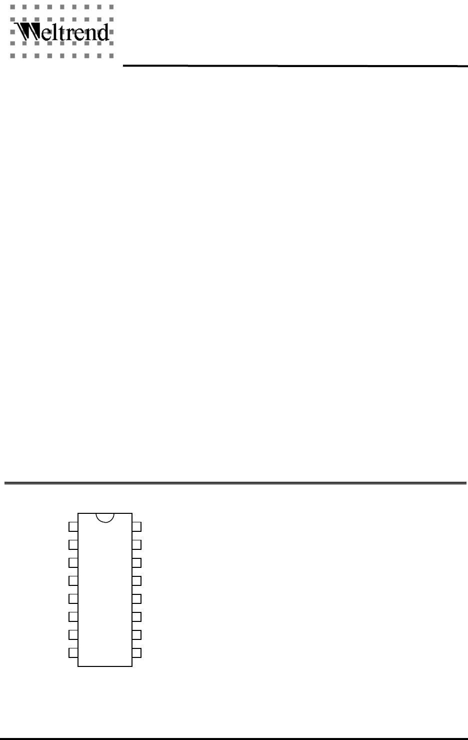
PIN ASSIGNMENT AND PACKAGE TYPE
Pin assignment
PGI
GND
FPOB
PSONB
I12A
RI
I12B
V12B
PGO
VCC
V5
V33
V12A
I33
I5
VX
16
15
14
13
12
11
10
9
1
2
3
4
5
6
7
8
WT7527
WT7527
Rev. 1.20
Weltrend Semiconductor, Inc.
Page 3
ORDERING INFORMATION
Part Number Package Type Note
WT7527–NN160–1D
WT7527–NN161–1D 16-Pin Plastic DIP, Pb-free
WT7527–SN160–1D
WT7527–SN161–1D 16-Pin Plastic SOP, Pb-free
PIN DESCRIPTION
Pin Name
I/O Description
PGI I Power good input signal pin
GND P Ground
FPOB O Fault protection output pin, open drain output
PSONB I On/Off switch input
I12A I 12VA over current protection sense input
RI I Current sense adjust input
I12B I 12VB over current protection sense input
V12B I 12VB over voltage & under voltage & over current sense input
pin
VX I Extra protection sense input
I5 I 5V over current protection sense input
I33 I 3.3V over current protection sense input
V12A I 12VA over voltage & under voltage & over current sense input
pin
V33 I 3.3V over voltage & under voltage & over current sense input pin
V5 I 5V over voltage & under voltage & over current sense input pin
VCC I Power supply
PGO O Power good output signal pin, open drain output
WT7527
Rev. 1.20
Weltrend Semiconductor, Inc.
Page 4
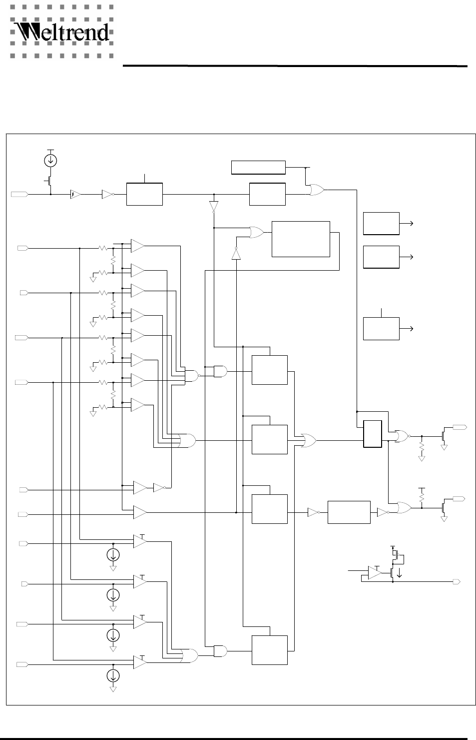
BLOCK DIAGRAM
WT7527-160
R
S Q
+
-
+
-
+
-
+
-
+
-
+
-
+
-
+
-
+
-
+
-
+
-
+
-
+
-
+
-
+
-
VCC
VCCI
PSONB
V33
V5
V12A
V12B
FPOB
VX
PGO
PGI
I33
RI
I5
I12A
I12B
60us
75ms / 600ms
delay
clr
1.2V ~ 1.8V
300ms
clr delay
clr
73us
debounce
20ms
clr
debounce
VREF = 1.2V
V12A
IREF=VREF / RI
V12A
clr
debounce
14us
debounce
clr
OV
4ms
Power On Reset
clr delay
38ms
IREF * 8
IREF * 8
IREF * 8
IREF * 8
V12A
V12A
V12A
V12A
VREF = 1.2V
UN
OV
Power
Reference
Internal
Bandgap
OSC
PWR
CLK
VCCI = 3.6V
VREF = 1.2V
PWR
PWR
debounce
UN
UN
OV
UN
OV
OV
WT7527
Rev. 1.20
Weltrend Semiconductor, Inc.
Page 5
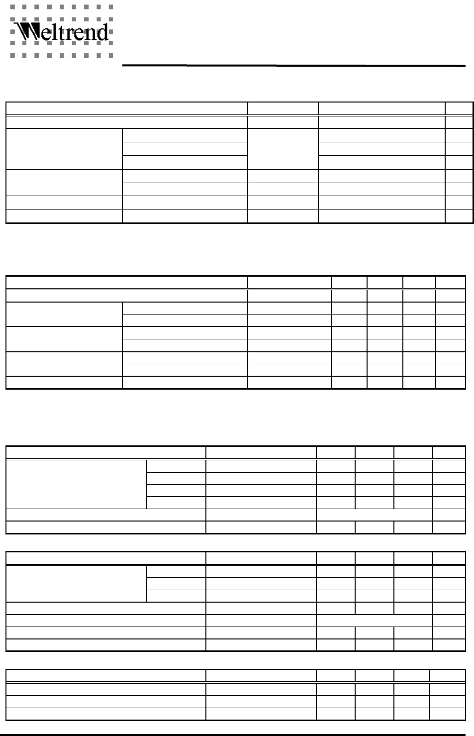
ABSOLUTE MAXIMUM RATINGS
Parameter Min. Max. Unit
Supply voltage, VCC, V12A –0.3 16 V
PGI, PSONB VCC + 0.3(Max. 7V) V
V5, I5, V33, I33 V12A + 0.3(Max. 7V) V
Input voltage
I12A, V12B, I12B
–0.3
V12A + 0.3(Max. 16V)
V
PGO –0.3 VCC + 0.3(Max. 7V) V
Output voltage FPOB –0.3 16 V
Operating temperature -40 125 ℃
Storage temperature -55 150 ℃
*Note: Stresses above those listed may cause permanent damage to the devices
RECOMMENDED OPERATING CONDITIONS
Parameter Conditions Min.
Typ.
Max.
Unit
Supply voltage, VCC 3.8 5 16 V
PGI, PSONB, V5, V33 7 V Input voltage
V12A, V12B 16 V
PGO 7 V Output voltage
FPOB 16 V
FPOB 0.3V 10 mA
Output sink current
PGO 0.3V 10 mA
Output current for RI RI 10 65 uA
ELECTRICAL CHARACTERISTICS,
at Ta=25°
°°
°C and V
CC
=5V
.
Over Voltage Detection
Parameter Condition Min. Typ. Max.
Unit
V33 3.8 3.9 4.0 V
V5 5.6 5.8 6.0 V
V12AB 13.5 13.85
14.2 V
Over voltage threshold
VX Use UVD timing 1.176
1.20 1.224
V
I
LEAKAGE
Leakage current (FPOB) V(FPOB) = 5V 5 uA
V
OL
Low level output voltage (FPOB) I
sink
=10mA 0.3 V
PGI and PGO
Parameter Condition Min. Typ. Max.
Unit
V33 2.8 2.9 3.0 V
V5 4.2 4.4 4.6 V
Under voltage threshold
V12AB 10.3 10.65
11.0 V
Input threshold voltage(PGI) 1.176
1.20 1.224
V
I
LEAKAGE
Leakage current(PGO) PGO = 5V 5 uA
V
OL
Low level output voltage(PGO) I
sink
=10mA 0.3 V
Offset Voltage of OCP comparators –6 6 mV
PSONB
Parameter Condition Min. Typ. Max.
Unit
Input pull-up current PSONB= 0V 150 uA
High-level input voltage 1.8 V
Low-level input voltage 1.2 V
WT7527
Rev. 1.20
Weltrend Semiconductor, Inc.
Page 6
TOTAL DEVICE
Parameter Condition Min. Typ. Max.
Unit
Icc Supply current PSONB= 5V 1 mA
Vcc operation start up voltage 3.2 3.4 3.6 V
Vcc under lockout voltage 2.8 3.0 3.2 V
SWITCHING CHARACTERISTICS, at Ta=-40℃
℃℃
℃~125℃
℃℃
℃
Parameter Condition Min. Typ. Max.
Unit
PGI to PGO Delay Time Td1 200 300 400 mS
Td2 49 75 100 mS
For 160 392 600 800 mS
Short circuit Delay Time Td2-1 For 161 ∞ mS
PGO to FPOB Delay Time Td3 2 4 6 mS
Under Voltage Delay Time Td4 40 60 81 µS
Over Current Delay Time Td5 13 20 27 mS
Over Voltage Delay Time Td6 9 14 19 uS
VX Delay Time Td7 40 60 81 µS
PSONB De-bounce Time Tb1 24 38 52 mS
PGI De-bounce Time Tb2 47 73 100 µS
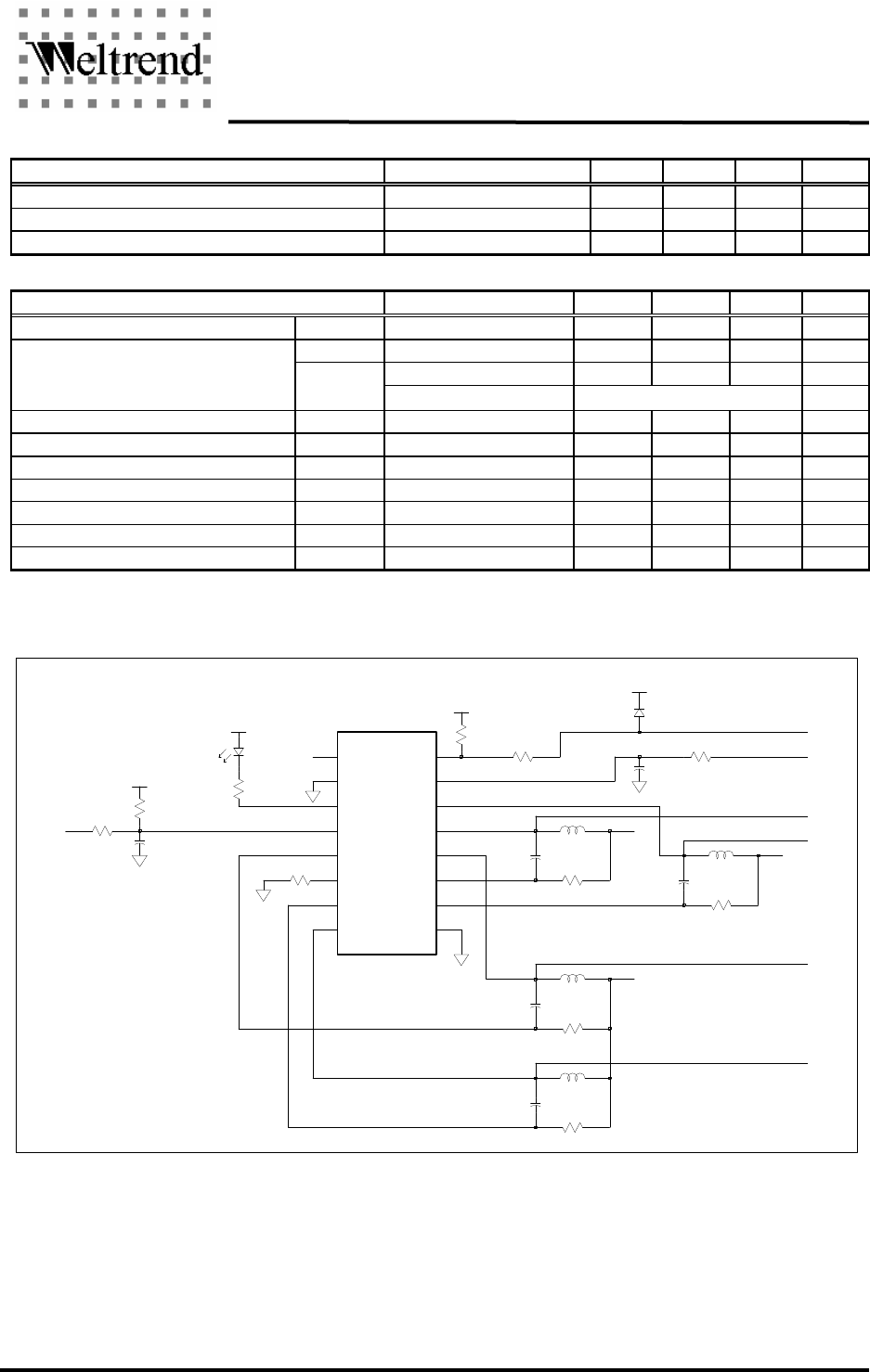
APPLICATION CIRCUIT
WT752701
I12B
I33
I5
PGI
PSONB
V12A
V12B
V33
V5
VCC
VX
FPOB
GND
I12A
PGO
RI
R16, 1%
22uF
+12VB
+12VA
22uF
R14, 1%
22uF
R10, 1%
R12, 1%
22uF
+5V
PSONB
+3.3V
D1
+5VSB
PGO
+5VSB
R5=300
1K
+5V
R4=100
30K, 1%
PGI
+5VSB
0.01uF
10K
+5VSB
NOTE1:The series resistor R5 at PSONB can not be omitted.(R5 = 300Ω is suggested)
NOTE2:The series resistor R4 = 100Ω and diode D1 at PGO is suggested.
WT7527
Rev. 1.20
Weltrend Semiconductor, Inc.
Page 7
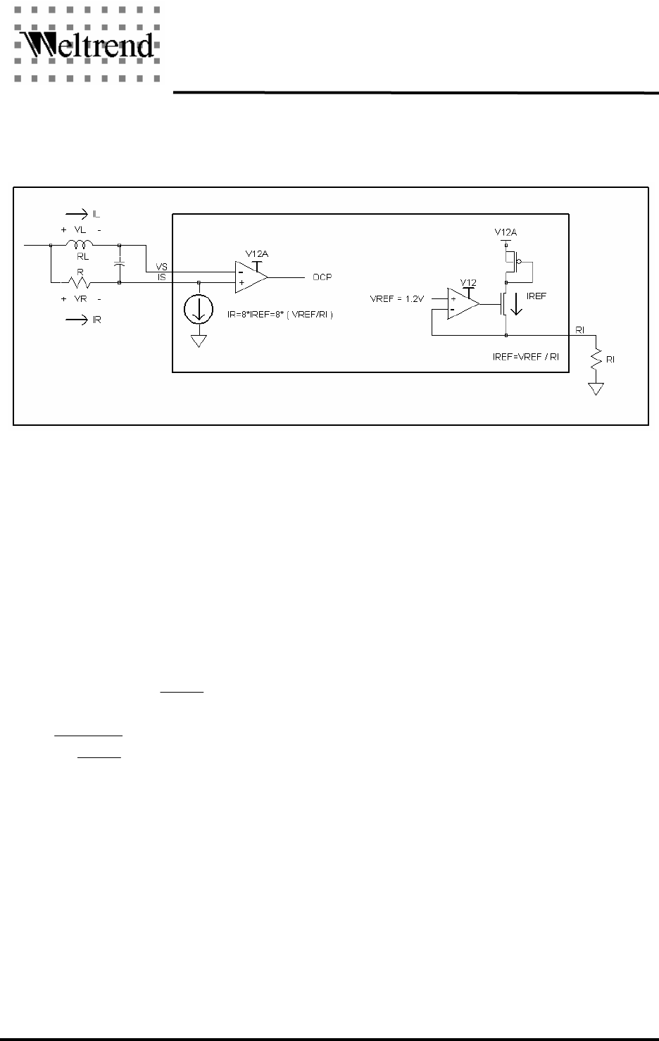
APPLICATION NOTE
When the load current increased, the voltage (VL) cross the inductor is increased.
And when inductor voltage exceeds the resistor voltage (VR), the OCP is active.
Sometimes power-on or load dynamics will cause false output of over-current detection. It can be
solved by connecting a capacitor between VS pin and IS pin. In typical case, C ≥ 0.47uF is suggested.
OCP point can be calculated by the following equation:
Let
VR = VL
IL
RL
IR
R
×
=
×
RI
VREF
IREFIR ×=×= 88Q
RI
VREF
ILRL
R
×
×
=∴
8
For example:
Assume RI=30KΩ, RL=5mΩ, OCP IL=20A.
Sol:
R = ( IL * RL ) / ( 8 * IREF )
= ( 20A * 5mΩ) / { 8 * ( 1.2V / 30KΩ)}
= 312.5Ω
WT7527
Rev. 1.20
Weltrend Semiconductor, Inc.
Page 8
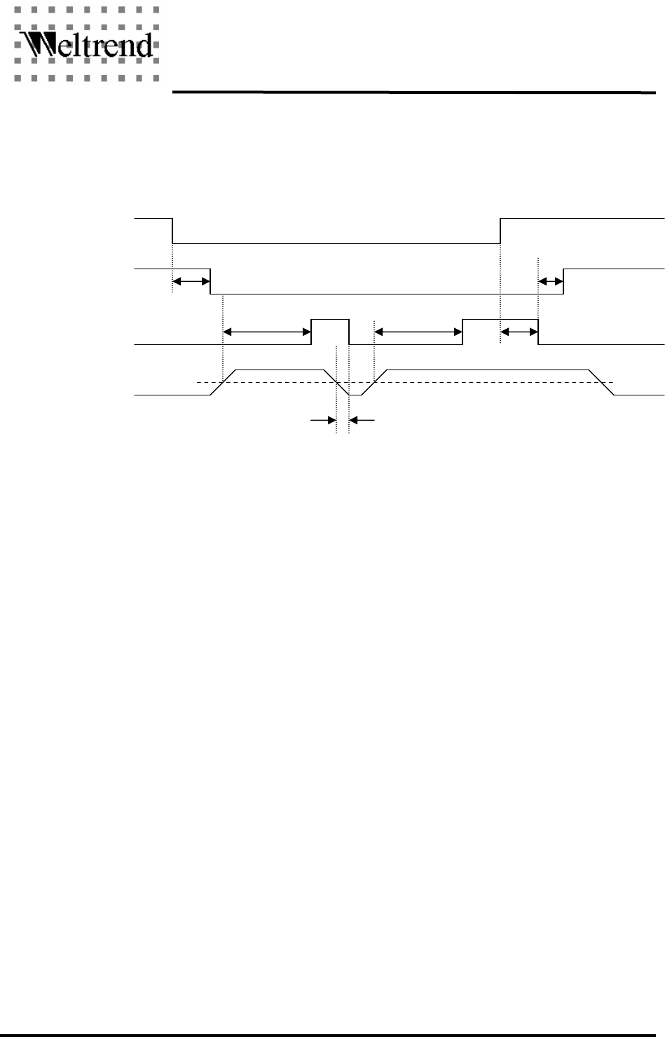
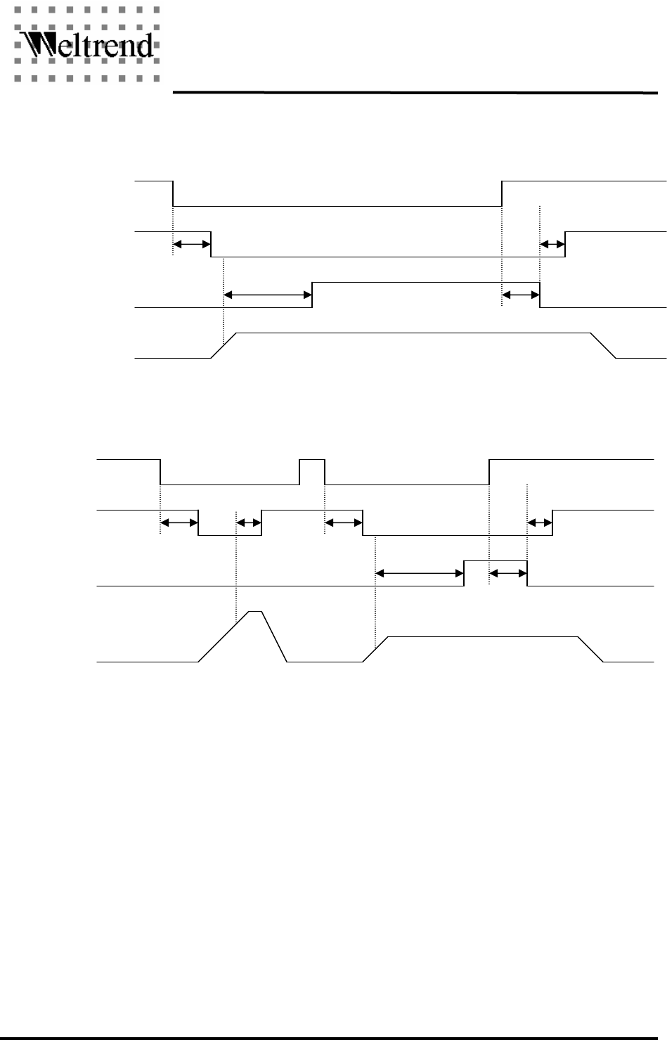
APPLICATION TIMMING
1.) PGI (UNDER_VOLTAGE):
::
:
PSONB
FPOB
PGO
PGI
t
b1
t
d1
+t
b2
t
b1
t
d3
t
d1
+t
b2
t
b2
WT7527
Rev. 1.20
Weltrend Semiconductor, Inc.
Page 9
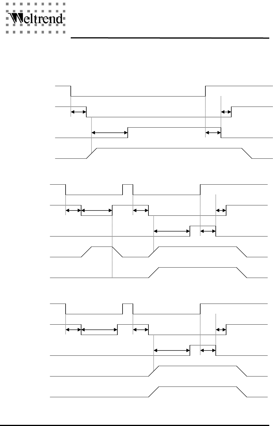
2.) V33, V5, V12 (UNDER_VOLTAGE) or I33, I5, I12 (OVER_CURRENT) or
VX (OVER_VOLTAGE):
::
:
PSONB
FPOB
PGO
V33/V5/V12
I33/I5/I12
/VX
t
b1
t
d1
+t
b2
t
b1
t
d3
PSONB
FPOB
PGO
PGI
V33/V5/V12
I33/I5/I12
/VX
t
b1
t
d1
+t
b2
t
b1
t
d3
t
d2
+t
d4
/
t
d5
/
t
d7
t
b1
t
d2
=
75
mS
t
b1
t
d1
+t
b2
t
b1
t
b3
t
d2-1
+t
d4
/
t
d5
/
t
d7
t
b1
PSONB
FPOB
PGO
PGI
V33/V5/V12
I33/I5/I12
/VX
t
d2-1
=
6
00mS
WT7527
Rev. 1.20
Weltrend Semiconductor, Inc.
Page 10
3.) V33, V5, V12 (OVER_VOLTAGE):
::
:
PSONB
FPOB
PGO
V33/V5/V12
t
b1
t
d1
+t
b2
t
b1
t
d3
PSONB
FPOB
PGO
V33/V5/V12
t
b1
t
d1
+t
b2
t
b1
t
d3
t
d6
t
b1
WT7527
Rev. 1.20
Weltrend Semiconductor, Inc.
Page 11
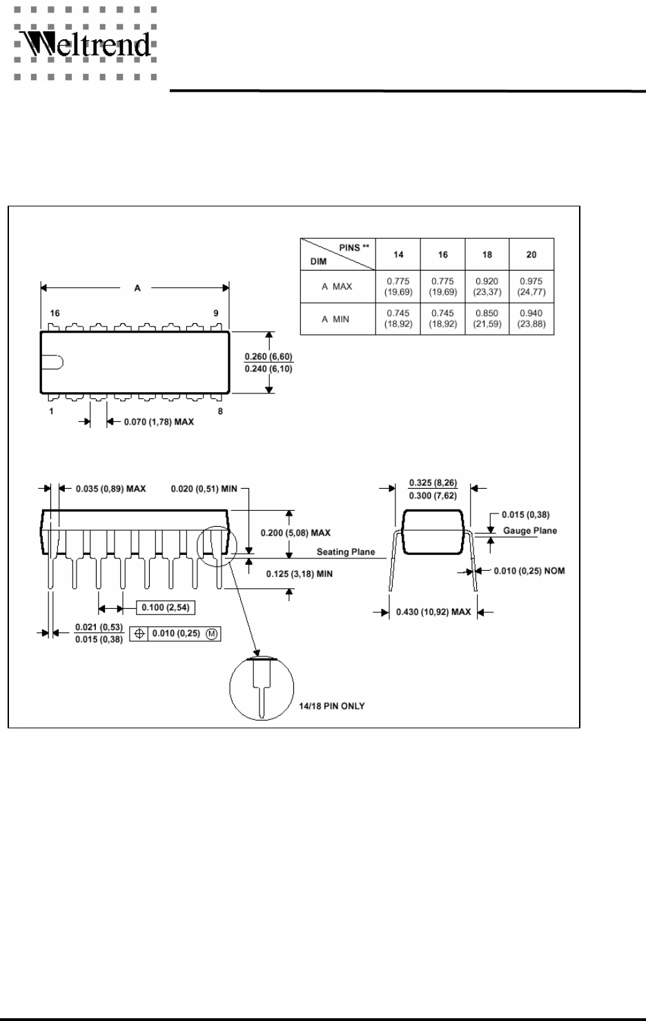
MECHANICAL INFORMATION
PLASTIC DUAL–IN–LINE PACKAGE
NOTE 1:All linear dimensions are in inches(millimeters).
NOTE 2:This drawing is subject to change without notice.
NOTE 3:Falls within JEDEC MS–001
WT7527
Rev. 1.20
Weltrend Semiconductor, Inc.
Page 12
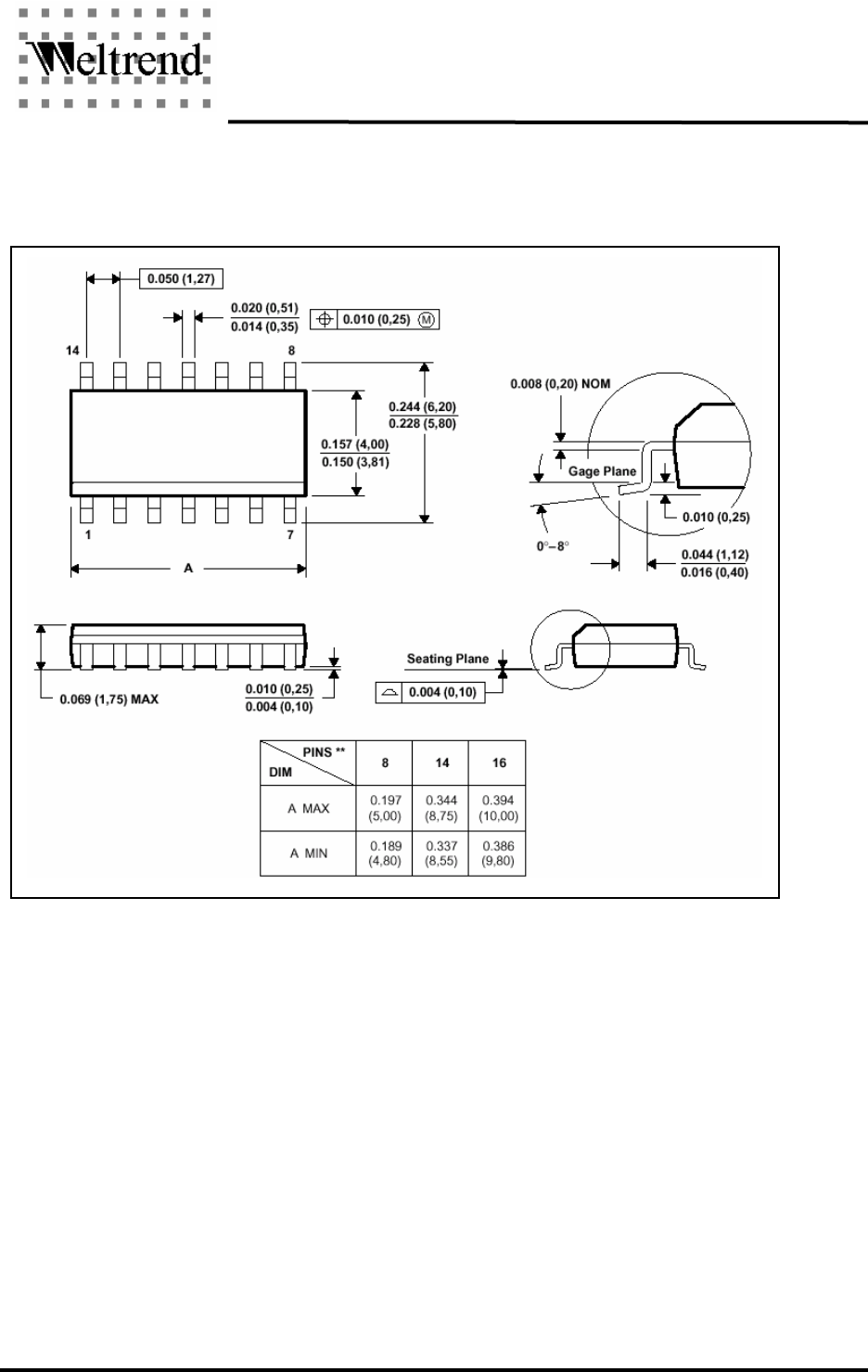
PLASTIC SMALL–OUTLINE PACKAGE
NOTE 1:All linear dimensions are in inches(millimeters).
NOTE 2:This drawing is subject to change without notice.
NOTE 3:Falls within JEDEC MS–012