XC6211, XC6219 Series Datasheet. Www.s Manuals.com. Torex
User Manual: Marking of electronic components, SMD Codes LX, LX-***, LX8*, LX9*, LXA*, LXB*, LXC*, LXD*, LXE*, LXF*, LXH*, LXJ, LXK*, LXL*, LXM*, LXN*, LXP, LXP*, LXR*, LXS*, LXT*, LXU*, LXV*, LXX*, LXY*, LXZ*. Datasheets 1SMB22AT3, P6SMB39A, PZU7.5B2A, RT9161A-32PV, SMBJ22A, TPSMB39A, TPSMB43A, XC6219B091MR, XC6219B091PR, XC6219B092MR, XC6219B092PR, XC6219B101MR, XC6219B101PR, XC6219B102MR, XC6219B102PR, XC6219B111MR, XC6219B111PR, XC6219B112MR, XC6219B112PR, XC6219B121MR, XC6219B121PR, XC6219B122MR, XC6219B122PR, XC62
Open the PDF directly: View PDF ![]() .
.
Page Count: 31
1/30
XC6219/XC6211 Series
300mA High Speed LDO Regulators with ON/OFF Switch
■
A
PPLICATIONS
●Mobile phones
●
Cordless phones, radio communication equipment
●Portable games
●Cameras, Video cameras
●Reference voltage sources
●Battery powered equipment
■GENERAL DESCRIPTION
The XC6219/XC6211 series are highly accurate, low noise, CMOS LDO Voltage Regulators. Offering low output noise, high
ripple rejection ratio, low dropout and very fast turn-on times, the XC6219/XC6211 series is ideal for today’s cutting edge
mobile phone.
Internally the XC6219/XC6211 includes a reference voltage source, error amplifiers, driver transistors, current limiters and
phase compensators. The XC6219/XC6211’s current limiters' foldback circuit also operates as a short protect for the output
current limiter and. the output pin. The output voltage is set by laser trimming. Voltages are selectable in 50mV steps
within a range of 0.9V to 5.0V. The XC6219/XC6211 series is also fully compatible with low ESR ceramic capacitors,
reducing cost and improving output stability. This high level of output stability is maintained even during frequent load
fluctuations, due to the excellent transient response performance and high PSRR achieved across a broad range of
frequencies.
The CE function allows the output of regulator to be turned off, resulting in greatly reduced power consumption.
■FEATURES
Maximum Output Current
Dropout Voltage
Operating Voltage Range
Output Voltage Range
Highly Accuracy
Low Power Consumption
Standby Current
High Ripple Rejection
Operating Ambient Temperature
Low ESR Capacitor
Ultra Small Packages
Environmentally Friendly
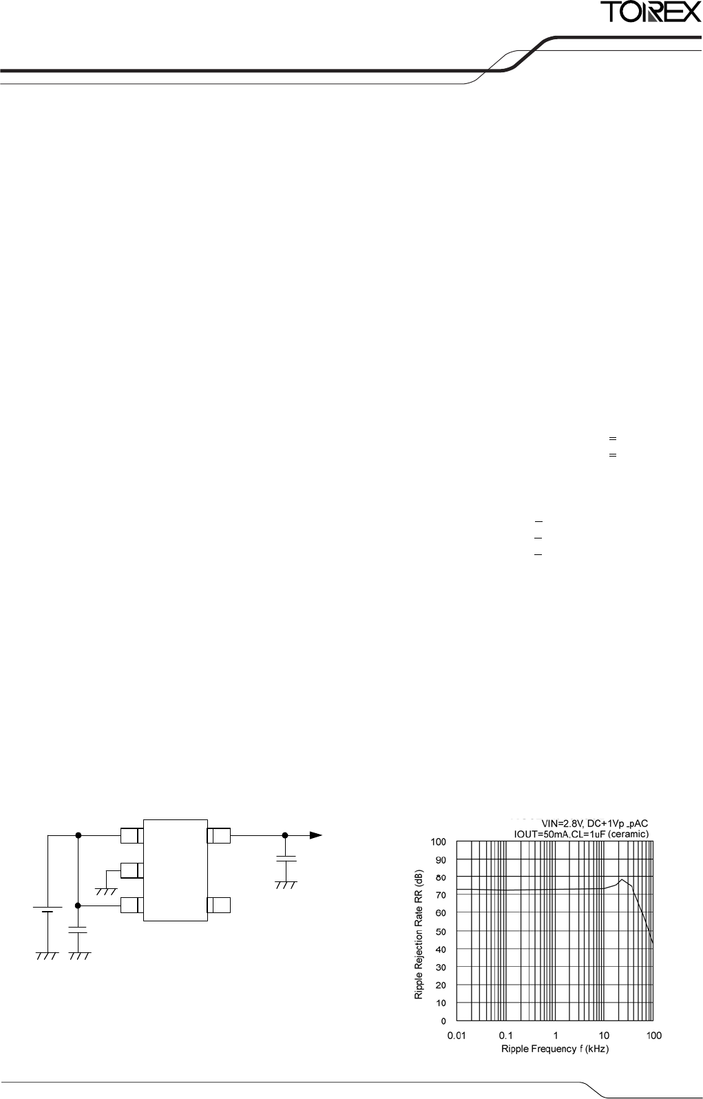
■TYPICAL APPLICATION CIRCUIT ■TYPICAL PERFORMANCE
CHARACTERISTICS
●Ripple Rejection Rate
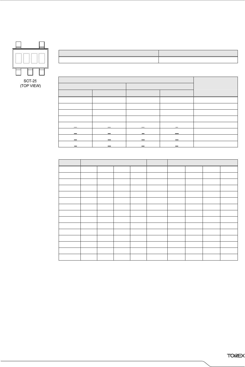
SOT-25
●XC6219 series
: 150mA (VOUT<1.75V, A~D type)
240mA (VOUT>1.8V, A~D type)
300mA (VOUT>1.3V, E~H type)
: 200mV @ 100mA
: 2.0V ~ 6.0V
: 0.9V ~ 5.0V (0.05V steps)
: +2% (VOUT>1.5V)
+30mV (VOUT≦1.5V)
+
1% (VOUT≧3.0V)
: 25μA (TYP.)
: Less than 0.1μA (TYP.)
: 65dB @10kHz
: -40℃ ~ 85℃
: Ceramic capacitor compatible
: SOT-25
SOT-89-5 (for XC6219 only)
USP-6B (for XC6219 only)
: EU RoHS Compliant, Pb Free
XC6219/XC6211
V
SS
1
2
34
5
V
IN
V
OUT
CE NC
C
IN
1μF
CL
1μF
ETR0307_009
2/30
XC6219/XC6211 Series
PIN NUMBER
XC6211 XC6219
SOT-25 SOT-25 SOT-89-5 USP-6B
PIN NAME FUNCTIONS
5 1 4 1 VIN Power Input
2 2 2 5 VSS Ground
1 3 3 6 CE ON / OFF Control
3 4 1 2, 4 NC No Connection
4 5 5 3 VOUT Output
TYPE A,E TYPE B,F
PIN NAME SIGNAL STATUS PIN NAME SIGNAL STATUS
L Stand-by L Stand-by
H Active H Active
CE
OPEN Stand-by
CE
OPEN Undefined state
TYPE C,G TYPE D,H
PIN NAME SIGNAL STATUS PIN NAME SIGNAL STATUS
L Active L Active
H Stand-by H Stand-by
CE
OPEN Stand-by
CE
OPEN Undefined state
*If XC6211/XC6219 B,D,F,H types are used with the CE pin opened, the IC goes into “Undefined state”.
The CE pin voltage should be fixed in low or high for stable operation.
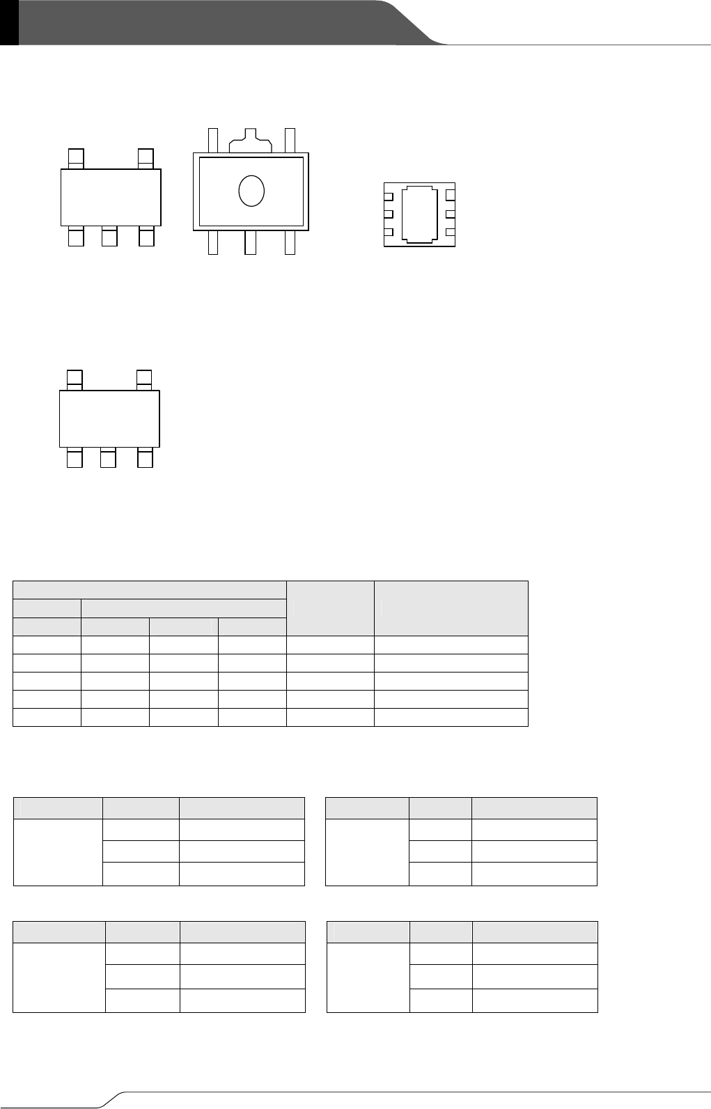
■PIN CONFIGURATION
SOT-25
(TOP VIEW)
4 5
1 2 3
VSS
NC
CE
VIN
VOUT
[XC6219 Series]
* The dissipation pad for the USP-6B
package should be solder-plated in
recommended mount pattern and
metal masking so as to enhance
mounting strength and hear release.
If the pad needs to be connected to
other pins, it should be connected to
the VSS pin.
VOUT
5
VSS
2
VIN
4
1
NC
2
VSS
3
CE
SOT-89-5
(TOP VIEW)
■PIN ASSIGNMENT
VSS 5
NC 4
CE 6 1 VIN
2 NC
3 VOUT
USP-6B
(BOTTOM VIEW)
■FUNCTION
[XC6211 Series]
45
12 3
VSS NCCE
VIN VOUT
SOT-25
(TOP VIEW)
3/30
XC6219/XC6211
Series
DESIGNATOR ITEM SYMBOL DESCRIPTION
A 150mA, High Active, pull-down resistor built in(*4) (Semi-custom)
B 150mA, High Active, no pull-down resistor built in (Standard)
C 150mA, Low Active, pull-up resistor built in(*4) (Semi-custom)
D 150mA, Low Active, no pull-up resistor built in (Semi-custom)
E 300mA, High Active, pull-down resistor built in(*4) (Semi-custom)
F 300mA, High Active, no pull-down resistor built in (Standard)
G 300mA, Low Active, pull-up resistor built in(*4) (Semi-custom)
① CE Pin Logic
H 300mA, Low Active, no pull-up resistor built in (Semi-custom)
②③ Output Voltage 09~50 e.g. ②=3, ③=0, → 3.0V
2(*3) 0.1V increments, ±2% accuracy
e.g. ③=2, ③=8, ④=2 → 2.80V, ±2%
1(*2) 0.1V increments, ±1% accuracy
e.g. ②=3, ③=0, ④=1 → 3.00V, ±1%
A(*3) 0.05V increments, ±2% accuracy
e.g. ②=2, ③=8, ④=A → 2.85V, ±2%
④ Output Voltage Accuracy
B(*2) 0.05V increments, ±1% accuracy
e.g. ②=3, ③=0, ④=B → 3.05V, ±1%
MR SOT-25(3,000/Reel)
MR-G SOT-25(3,000/Reel)
PR SOT-89-5 (for XC6219 only) (1,000/Reel)
PR-G SOT-89-5 (for XC6219 only) (1,000/Reel)
DR USP-6B (for XC6219 only) (3,000/Reel)
⑤⑥-⑦ Packages
(Order Unit)
DR-G USP-6B (for XC6219 only) (3,000/Reel)
■PRODUCT CLASSIFICATION
●Ordering Information
XC6219 ①②③④⑤⑥-⑦(*1)(Standard pin layout versions)
XC6211 ①②③④⑤⑥-⑦(*1)(Different pin layout version in SOT-25)
(*1) The “-G” suffix denotes Halogen and Antimony free as well as being fully RoHS compliant.
(*2) Output voltage of the ±1% accuracy product is 3.0V or more.
(*3) Output voltage accuracy of the VOUT≦1.5V is ±30mV.
(*4) With the pull-up resistor or pull-down resistor built-in types, the supply current during operation will increase by VIN / 2.0MΩ (TYP.)
4/30
XC6219/XC6211 Series
*Diode inside the circuit are an ESD protection diode and a parasitic diode.
PARAMETER SYMBOL RATINGS UNITS
Input Voltage VIN 7 V
Output Current IOUT 500(*1) mA
Output Voltage VOUT VSS - 0.3 ~ VIN + 0.3 V
CE Pin Voltage VCE VSS - 0.3 ~ VIN + 0.3 V
250
SOT-25 600 (PCB mounted)(*2)
500
mW
SOT-89 1300 (PCB mounted)(*2)
120
Power Dissipation
USP-6B
Pd
1000 (PCB mounted)(*2)
Operating Ambient Temperature Topr - 40 ~ + 85 ℃
Storage Temperature Tstg - 55 ~ + 125 ℃
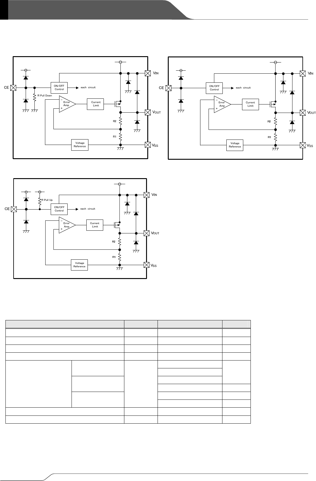
■BLOCK DIAGRAM
■
A
BSOLUTE MAXIMUM RATINGS
Ta=25℃
XC6211,XC6219 series Type A,E XC6211,XC6219 series Type B,D,F,H
XC6211,XC6219 series Type C,G
All voltages are described based on the VSS pin.
(*1) IOUT≦Pd/(VIN-VOUT)
(*2) The power dissipation figure shown is PCB mounted and is for reference only. Please refer to page 24~26 for details.

5/30
XC6219/XC6211
Series
PARAMETER SYMBOL CONDITIONS MIN. TYP. MAX. UNITS CIRCUIT
Output Voltage (*5)
(2%)
VOUT(T)
(*2)
×0.98 VOUT(T)
(*2) VOUT(T)
(*2)
×1.02
Output Voltage (*6)
(1%)
VOUT(E)
(*3) I
OUT=30mA
VOUT(T)
(*2)
×0.99 VOUT(T)
(*2) VOUT(T)
(*2)
×1.01
V ①
0.9V≦VOUT(T)≦1.75V 150 - -
Maximum Output
Current IOUTMAX
1.8V≦VOUT(T)≦5.0V 240 - -
mA ①
Load Regulation ΔVOUT 1mA≦IOUT≦100mA - 15 50 mV
①
Vdif1 IOUT=30mA - E-1
Dropout Voltage (*4)
Vdif2 IOUT=100mA - E-2
mV ①
Supply Current
(Type A) - 28 55
Supply Current
(Type B)
IDD VCE=VIN=VOUT(T)+1.0V
VOUT≦0.95V, VIN=VCE=2.0V
- 25 50
μA ②
Stand-by Current ISTB VIN=VOUT(T)+1.0V、VCE=VSS
VOUT≦0.95V, VIN=2.0V - 0.01 0.10 μA ②
Line Regulation
ΔVOUT/
(ΔVIN・VOUT)
VOUT(T)+1.0V≦VIN≦6.0V
VOUT≦0.95V, 2.0V≦VIN≦6.0V
IOUT=30mA
VOUT≦1.75V, IOUT=10mA
- 0.01 0.20 %/V ①
Input Voltage VIN - 2 - 6 V -
Output Voltage
Temperature
Characteristics
ΔVOUT/
(ΔTopr・VOUT)
IOUT=30mA
-40℃≦Topr≦85℃ - ±100 -
ppm/℃ ①
Power Supply
Rejection Ratio PSRR
VIN=[VOUT(T)+1.0]V+1.0Vp-pAC
VOUT≦1.5, VIN=2.5V+1.0Vp-pAC
IOUT=50mA、f=10kHz
- E-3 - dB
④
VIN=VOUT(T)+2.0V、VCE=VIN
0.9V≦VOUT(T)≦1.75V - 300 -
Current Limiter Ilim
VIN=VOUT(T)+1.0V、VCE=VIN
1.8V≦VOUT(T)≦5.0V 240 300 -
mA ①
Short Circuit Current ISHORT VIN=VOUT(T)+1.0V、 VCE=VIN
VOUT≦1.75V, VIN=VOUT(T)+2.0V - 50 - mA
①
CE ‘High’ Level Voltage VCEH - 1.6 - VIN V ①
CE ‘Low’ Level Voltage VCEL - - - 0.25 V ①
CE ‘High’ Level Current
(Type A) -0.10 - 5.0
CE ‘High’ Level Current
(Type B)
ICEH VIN=VCE=VOUT(T)+1.0V
VOUT≦0.95V, VIN=VCE=2.0V
-0.10 - 0.10
μA ②
CE ‘Low’ Level Current ICEL VIN=VOUT(T)+1.0V、VCE=VSS
VOUT≦0.95V, VIN=2.0V -0.10 - 0.10 μA ②
■ELECTRICAL CHARACTERISTICS
Ta=25℃
●XC6219/XC6211 Type A,B
(*1) Unless otherwise stated, VIN=VOUT(T)+1.0V. If VOUT is less than 0.95V, VIN= 2.0V.
(*2) VOUT(T) = Specified output voltage
(*3) VOUT(E) = Effective output voltage
The output voltage when "VOUT(T)+1.0V" is provided at the VIN pin while maintaining a certain IOUT value.
(*4) Vdif={VIN1-VOUT1
}
VOUT1=A voltage equal to 98% of the output voltage whenever an amply stabilized IOUT {VOUT(T)+1.0V} is input.
VIN1=The Input Voltage when VOUT1 appears as Input Voltage is gradually decreased.
(*5)If VOUT(T) is less than 1.45V, VOUT(T) -30mV (MIN.), VOUT(T) + 30mV (MAX.)
(*6)Only for the VOUT(T) is more than 3.0V products.

6/30
XC6219/XC6211 Series
PARAMETER SYMBOL CONDITIONS MIN. TYP. MAX. UNITS CIRCUIT
Output Voltage (*5)
(2%)
VOUT(T)
(*2)
×0.98 VOUT(T)
(*2) VOUT(T)
(*2)
×1.02
Output Voltage (*6)
(1%)
VOUT(E)
(*3) I
OUT=30mA
VOUT(T)
(*2)
×0.99 VOUT(T)
(*2) VOUT(T)
(*2)
×1.01
V ①
0.9V≦VOUT(T)≦1.75V 150 - -
Maximum Output
Current IOUTMAX
1.8V≦VOUT(T)≦5.0V 240 - -
mA ①
Load Regulation ΔVOUT 1mA≦IOUT≦100mA - 15 50 mV
①
Vdif1 IOUT=30mA - E-1
Dropout Voltage (*4)
Vdif2 IOUT=100mA - E-2
mV ①
Supply Current
(Type C) - 28 55
Supply Current
(Type D)
IDD
VIN=VOUT(T)+1.0V
VOUT≦0.95V, VIN=2.0V
VCE=VSS - 25 50
μA ②
Stand-by Current ISTB VIN=VOUT(T)+1.0V、VCE=VIN
VOUT≦0.95V, VIN=VCE=2.0V - 0.01 0.10 μA ②
Line Regulation
ΔVOUT/
(ΔVIN・VOUT)
VOUT(T)+1.0V≦VIN≦6.0V
VOUT≦0.95V, 2.0V≦VIN≦6.0V
IOUT=30mA
VOUT≦1.75V, IOUT=10mA
- 0.01 0.20 %/V ①
Input Voltage VIN - 2 - 6 V -
Output Voltage
Temperature
Characteristics
ΔVOUT/
(ΔTopr・VOUT)
IOUT=30mA
-40℃≦Topr≦85℃ - ±100 -
ppm/℃ ①
Power Supply
Rejection Ratio PSRR
VIN=[VOUT(T)+1.0]V+1.0Vp-pAC
VOUT≦1.5, VIN=2.5V+1.0Vp-pAC
IOUT=50mA、f=10kHz
- E-3 - dB
④
VIN=VOUT(T)+2.0V、VCE=VSS
0.9V≦VOUT(T)≦1.75V - 300 -
Current Limiter Ilim
VIN=VOUT(T)+1.0V、VCE=VSS
1.8V≦VOUT(T)≦5.0V 240 300 -
mA ①
Short Circuit Current ISHORT VIN=VOUT(T)+1.0V、 VCE=VIN
VOUT≦1.75V, VIN=VOUT(T)+2.0V - 50 - mA
①
CE ‘High’ Level Voltage VCEH - 1.6 - VIN V ①
CE ‘Low’ Level Voltage VCEL - - - 0.25 V ①
CE ‘High’ Level Current ICEH VCE=VIN=VOUT(T)+1.0V
VOUT≦0.95V, VCE=VIN=2.0V -0.10 - 0.10
μA ②
CE ‘Low’ Level Current
(Type C) -5.0 - 0.10
CE ‘Low’ Level Current
(Type D)
ICEL VIN=VOUT(T)+1.0V,VCE=VSS
VOUT≦0.95V, VIN=2.0V
-0.10 - 0.10
μA ②
■ELECTRICAL CHARACTERISTICS
●XC6219/XC6211 Type C,D
(*1) Unless otherwise stated, VIN=VOUT(T)+1.0V. If VOUT is less than 0.95V, VIN= 2.0V.
(*2) VOUT(T) = Specified output voltage
(*3) VOUT(E) = Effective output voltage
The output voltage when "VOUT(T)+1.0V" is provided at the VIN pin while maintaining a certain IOUT value.
(*4) Vdif={VIN1-VOUT1
}
VOUT1=A voltage equal to 98% of the output voltage whenever an amply stabilized IOUT {VOUT(T)+1.0V} is input.
VIN1=The Input Voltage when VOUT1 appears as Input Voltage is gradually decreased.
(*5)If VOUT(T) is less than 1.45V, VOUT(T) -30mV (MIN.), VOUT(T) + 30mV (MAX.)
(*6)Only for the VOUT(T) is more than 3.0V products.
Ta=25℃
7/30
XC6219/XC6211
Series
PARAMETER SYMBOL CONDITIONS MIN. TYP. MAX. UNITS CIRCUIT
Output Voltage (*5)
(2%)
VOUT(T)
(*2)
×0.98 VOUT(T)
(*2) VOUT(T)
(*2)
×1.02
Output Voltage (*6)
(1%)
VOUT(E)
(*3) I
OUT=30mA
VOUT(T)
(*2)
×0.99 VOUT(T)
(*2) VOUT(T)
(*2)
×1.01
V ①
Maximum Output
Current IOUTMAX V
IN=E-5 (*7) E-4 - - mA
①
Load Regulation ΔVOUT 1mA≦IOUT≦100mA - 15 50 mV
①
Load Regulation2 ΔVOUT2 1mA≦IOUT≦300mA - - 100 mV
①
Vdif1 IOUT=30mA - E-1
Dropout Voltage (*4)
Vdif2 IOUT=100mA - E-2
mV ①
Supply Current
(Type E) - 28 55
Supply Current
(Type F)
IDD VCE=VIN=VOUT(T)+1.0V
VOUT≦0.95V, VCE=VIN=2.0V
- 25 50
μA ②
Stand-by Current ISTB VIN=VOUT(T)+1.0V、VCE=VSS
VOUT≦0.95V, VCE=VIN=2.0V - 0.01 0.10 μA ②
Line Regulation
ΔVOUT/
(ΔVIN・VOUT)
VOUT(T)+1.0V≦VIN≦6.0V
VOUT≦0.95V, 2.0V≦VIN≦6.0V
IOUT=30mA
VOUT≦1.75V, IOUT=10mA
- 0.01 0.20 %/V ①
Input Voltage VIN - 2 - 6 V -
Output Voltage
Temperature
Characteristics
ΔVOUT/
(ΔTopr・VOUT)
IOUT=30mA
-40℃≦Topr≦85℃ - ±100 -
ppm/℃ ①
Power Supply
Rejection Ratio PSRR
VIN=[VOUT(T)+1.0]V+1.0Vp-pAC
VOUT≦1.5, VIN=2.5V+1.0Vp-pAC
IOUT=50mA、f=10kHz
- 70 - dB
④
VIN=VOUT(T)+2.0V、VCE=VIN
0.9V≦VOUT(T)≦1.75V
Current Limiter Ilim
VIN=VOUT(T)+1.0V、VCE=VIN
1.8V≦VOUT(T)≦5.0V
- 380 - mA
①
Short Circuit Current ISHORT VIN=VOUT(T)+1.0V、 VCE=VIN
VOUT≦1.75V, VIN=VOUT(T)+2.0V - 50 - mA
①
CE ‘High’ Level Voltage VCEH - 1.6 - VIN V ①
CE ‘Low’ Level Voltage VCEL - - - 0.25 V ①
CE ‘High’ Level Current
(Type E) -0.10 - 5.0
CE ‘High’ Level Current
(Type F)
ICEH VIN=VCE=VOUT(T)+1.0V
VOUT≦0.95V, VIN=VCE=2.0V
-0.10 - 0.10
μA ②
CE ‘Low’ Level Current ICEL VIN=VOUT(T)+1.0V、VCE=VSS
VOUT≦0.95V, VIN=2.0V -0.1 - 0.1
μA ②
■ELECTRICAL CHARACTERISTICS
●XC6219/XC6211 Type E,F Ta=25℃
(*1) Unless otherwise stated, VIN=VOUT(T)+1.0V. If VOUT is less than 0.95V, VIN= 2.0V.
(*2) VOUT(T) = Specified output voltage
(*3) VOUT(E) = Effective output voltage
The output voltage when "VOUT(T)+1.0V" is provided at the VIN pin while maintaining a certain IOUT value.
(*4) Vdif={VIN1-VOUT1
}
VOUT1=A voltage equal to 98% of the output voltage whenever an amply stabilized IOUT {VOUT(T)+1.0V} is input.
VIN1=The Input Voltage when VOUT1 appears as Input Voltage is gradually decreased.
(*5)If VOUT(T) is less than 1.45V, VOUT(T) -30mV (MIN.), VOUT(T) + 30mV (MAX.)
(*6)Only for the VOUT(T) is more than 3.0V products.
(*7)Please refer to the “Voltage Chart” table.
8/30
XC6219/XC6211 Series
PARAMETER SYMBOL CONDITIONS MIN. TYP. MAX. UNITS CIRCUIT
Output Voltage (*5)
(2%)
VOUT(T)
(*2)
×0.98 VOUT(T)
(*2) VOUT(T)
(*2)
×1.02
Output Voltage (*6)
(1%)
VOUT(E)
(*3) I
OUT=30mA
VOUT(T)
(*2)
×0.99 VOUT(T)
(*2) VOUT(T)
(*2)
×1.01
V ①
Maximum Output
Current IOUTMAX V
IN=E-5 (*7) E-4 - - mA
①
Load Regulation ΔVOUT 1mA≦IOUT≦100mA - 15 50 mV
①
Load Regulation2 ΔVOUT2 1mA≦IOUT≦300mA - - 100 mV
①
Vdif1 IOUT=30mA - E-1
Dropout Voltage (*4)
Vdif2 IOUT=100mA - E-2
mV ①
Supply Current
(Type G) - 28 55
Supply Current
(Type H)
IDD
VCE=VIN=VOUT(T)+1.0V
VOUT≦0.95V, VIN=2.0V
VCE=VSS - 25 50
μA ②
Stand-by Current ISTB VIN=VOUT(T)+1.0V、VCE=VIN
VOUT≦0.95V, VCE=VIN=2.0V - 0.01 0.10 μA ②
Line Regulation
ΔVOUT/
(ΔVIN・VOUT)
VOUT(T)+1.0V≦VIN≦6.0V
VOUT≦0.95V, 2.0V≦VIN≦6.0V
IOUT=30mA
VOUT≦1.75V, IOUT=10mA
- 0.01 0.20 %/V ①
Input Voltage VIN - 2 - 6 V -
Output Voltage
Temperature
Characteristics
ΔVOUT/
(ΔTopr・VOUT)
IOUT=30mA
-40℃≦Topr≦85℃ - ±100 -
ppm/℃ ①
Power Supply
Rejection Ratio PSRR
VIN=[VOUT(T)+1.0]V+1.0Vp-pAC
VOUT≦1.5, VIN=2.5V+1.0Vp-pAC
IOUT=50mA、f=10kHz
- 70 - dB
④
VIN=VOUT(T)+2.0V、VCE=VSS
0.9V≦VOUT(T)≦1.75V
Current Limiter Ilim
VIN=VOUT(T)+1.0V、VCE=VSS
1.8V≦VOUT(T)≦5.0V
- 380 - mA
①
Short Circuit Current ISHORT VIN=VOUT(T)+1.0V、 VCE=Vss
VOUT≦1.75V, VIN=VOUT(T)+2.0V - 50 - mA
①
CE ‘High’ Level Voltage VCEH - 1.6 - VIN V ①
CE ‘Low’ Level Voltage VCEL - - - 0.25 V ①
CE ‘High’ Level Current ICEH VCE=VIN=VOUT(T)+1.0V
VOUT≦0.95V, VCE=VIN=2.0V -0.10 - 0.10
μA ②
CE ‘Low’ Level Current
(Type G) -5.0 - 0.10
CE ‘Low’ Level Current
(Type H)
ICEL VIN=VOUT(T)+1.0V、VCE=VSS
VOUT≦0.95V, VIN=2.0V
-0.10 - 0.10
μA ②
■ELECTRICAL CHARACTERISTICS
●XC6219/XC6211 Type G,H
(*1) Unless otherwise stated, VIN=VOUT(T)+1.0V. If VOUT is less than 0.95V, VIN= 2.0V.
(*2) VOUT(T) = Specified output voltage
(*3) VOUT(E) = Effective output voltage
The output voltage when "VOUT(T)+1.0V" is provided at the VIN pin while maintaining a certain IOUT value.
(*4) Vdif={VIN1-VOUT1
}
VOUT1=A voltage equal to 98% of the output voltage whenever an amply stabilized IOUT {VOUT(T)+1.0V} is input.
VIN1=The Input Voltage when VOUT1 appears as Input Voltage is gradually decreased.
(*5)If VOUT(T) is less than 1.45V, VOUT(T) -30mV (MIN.), VOUT(T) + 30mV (MAX.)
(*6)Only for the VOUT(T) is more than 3.0V products.
(*7)Please refer to the “Voltage Chart” table.
Ta=25℃
9/30
XC6219/XC6211
Series
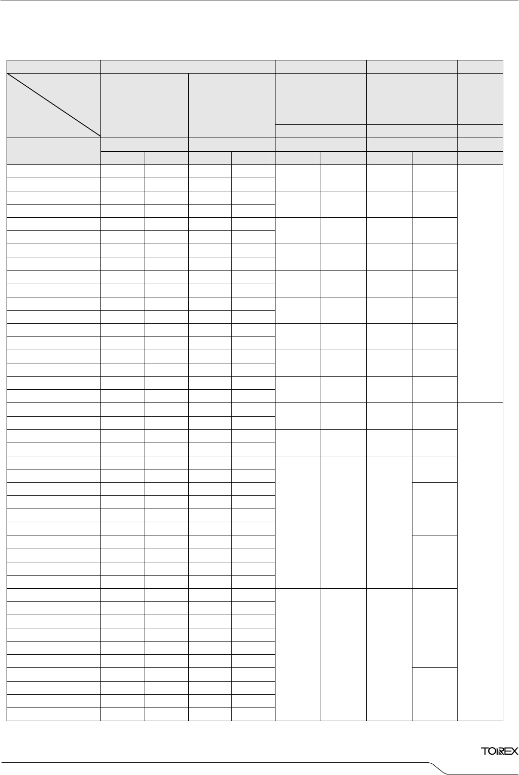
SYMBOL E-0 E-1 E-2 E-3
PARAMETER
DROPOUT
VOLTAGE1 (mV)
(IOUT=30mA)
DROPOUT
VOLTAGE2 (mV)
(IOUT=100mA)
Power
Supply
Rejection
Ratio
OUTPUT VOLTAGE
OUTPUT VOLTAGE
(2%)
(V)
OUTPUT VOLTAGE
(1%)
(V)
Ta=25℃ Ta=25℃ Ta=25℃
VOUT VOUT Vdif1 Vdif2 PSRR
VOUT(T) MIN MAX MIN MAX TYP MAX TYP MAX TYP
0.90 0.870 0.930 - -
0.95 0.920 0.980 - - 1100 1110 1150 1200
1.00 0.970 1.030 - -
1.05 1.020 1.080 - - 1000 1010 1050 1100
1.10 1.070 1.130 - -
1.15 1.120 1.180 - - 900 910 950 1000
1.20 1.170 1.230 - -
1.25 1.220 1.280 - - 800 810 850 900
1.30 1.270 1.330 - -
1.35 1.320 1.380 - - 700 710 750 800
1.40 1.370 1.430 - -
1.45 1.420 1.480 - - 600 610 650 700
1.50 1.470 1.530 - -
1.55 1.519 1.581 - - 500 510 550 600
1.60 1.568 1.632 - -
1.65 1.617 1.683 - - 400 410 500 550
1.70 1.666 1.734 - -
1.75 1.715 1.785 - - 300 310 400 450
65
1.80 1.764 1.836 - -
1.85 1.813 1.887 - - 200 210 300 400
1.90 1.862 1.938 - -
1.95 1.911 1.989 - - 120 150 280 380
2.00 1.960 2.040 - -
2.05 2.009 2.091 - - 350
2.10 2.058 2.142 - -
2.15 2.107 2.193 - -
2.20 2.156 2.244 - -
2.25 2.205 2.295 - -
330
2.30 2.254 2.346 - -
2.35 2.303 2.397 - -
2.40 2.352 2.448 - -
2.45 2.401 2.499 - -
80 120 240
310
2.50 2.450 2.550 - -
2.55 2.499 2.601 - -
2.60 2.548 2.652 - -
2.65 2.597 2.703 - -
2.70 2.646 2.754 - -
2.75 2.695 2.805 - -
290
2.80 2.744 2.856 - -
2.85 2.793 2.907 - -
2.90 2.842 2.958 - -
2.95 2.891 3.009 - -
70 100 220
270
70
■ELECTRICAL CHARACTERISTICS (Continued)
●Voltage Chart
10/30
XC6219/XC6211 Series
SYMBOL E-0 E-1 E-2 E-3
PARAMETER
DROPOUT
VOLTAGE1 (mV)
(IOUT=30mA)
DROPOUT
VOLTAGE2 (mV)
(IOUT=100mA)
Power
Supply
Rejection
Ratio
OUTPUT VOLTAGE
OUTPUT VOLTAGE
(2%)
(V)
OUTPUT VOLTAGE
(1%)
(V)
Ta=25℃ Ta=25℃ Ta=25℃
VOUT VOUT Vdif1 Vdif2 PSRR
VOUT(T) MIN MAX MIN MAX TYP MAX TYP MAX TYP
3.00 2.940 3.060 2.970 3.030
3.05 2.989 3.111 3.020 3.081 270
3.10 3.038 3.162 3.069 3.131
3.15 3.087 3.213 3.119 3.182
3.20 3.136 3.264 3.168 3.232
3.25 3.185 3.315 3.218 3.283
3.30 3.234 3.366 3.267 3.333
3.35 3.283 3.417 3.317 3.384
3.40 3.332 3.468 3.366 3.434
3.45 3.381 3.519 3.416 3.485
3.50 3.430 3.570 3.465 3.535
3.55 3.479 3.621 3.515 3.586
3.60 3.528 3.672 3.564 3.636
3.65 3.577 3.723 3.614 3.687
3.70 3.626 3.774 3.663 3.737
3.75 3.675 3.825 3.713 3.788
3.80 3.724 3.876 3.762 3.838
3.85 3.773 3.927 3.812 3.889
3.90 3.822 3.978 3.861 3.939
3.95 3.871 4.029 3.911 3.990
90 200
250
4.00 3.920 4.080 3.960 4.040
4.05 3.969 4.131 4.010 4.091
4.10 4.018 4.182 4.059 4.141
4.15 4.067 4.233 4.109 4.192
4.20 4.116 4.284 4.158 4.242
4.25 4.165 4.335 4.208 4.293
4.30 4.214 4.386 4.257 4.343
4.35 4.263 4.437 4.307 4.394
4.40 4.312 4.488 4.356 4.444
4.45 4.361 4.539 4.405 4.494
4.50 4.410 4.590 4.455 4.545
4.55 4.459 4.641 4.504 4.595
4.60 4.508 4.692 4.554 4.646
4.65 4.557 4.743 4.603 4.696
4.70 4.606 4.794 4.653 4.747
4.75 4.655 4.845 4.702 4.797
4.80 4.704 4.896 4.752 4.848
4.85 4.753 4.947 4.801 4.898
4.90 4.802 4.998 4.851 4.949
4.95 4.851 5.049 4.900 4.999
60
80 180 230
5.00 4.900 5.100 4.950 5.050 50 70 160 210
70
■ELECTRICAL CHARACTERISTICS (Continued)
●Voltage Chart
11/30
XC6219/XC6211
Series
SYMBOL E-5 E-4
INPUT VOLTAGE (V) MAX. OUTPUT CURRENT
(mA)
CONDITION, RATINGS
OUTPUT VOLTAGE (V) VIN MIN
0.90~0.95 2.5 260
1.00~1.05 2.5 260
1.10~1.15 2.6 270
1.20~1.25 2.7 290
1.30~1.35 2.8
1.40~1.45 2.9
1.50~1.95 3.0
2.00~6.00 VOUT(T)+1.0
300
* VOUT(T)=Nominal output voltage
■ELECTRICAL CHARACTERISTICS (Continued)
●Specification & Condition by Series
12/30
XC6219/XC6211 Series
*TEST CIRCUIT VCE (CE Pin Voltage)
ACTIVE
XC6211/XC6219 Type A,B,E,F: VCE=VIN
XC6211/XC6219 Type C,D,G,H: VCE=VSS
STANDBY
XC6211/XC6219 Type A,B,E,F: VCE=VSS
XC6211/XC6219 Type C,D,G,H: VCE=VIN
■TEST CIRCUITS
Circuit ①
Circuit ②
Circuit ③
Circuit ④
VIN VOUT
VSS
CE
CIN=1.0uF
(セラミック)
CL=1.0uF
(セラミック)
F.F.T
IOUT=10mA
VCE
ceram
i
c
ceram
i
c
ceram
i
c
ceram
i
c
ceram
i
c
13/30
XC6219/XC6211
Series
■OPERATIONAL EXPLANATION
<Output Voltage Control>
The voltage divided by resistors R1 & R2 is compared with the internal reference voltage by the error amplifier. The
P-channel MOSFET, which is connected to the VOUT pin, is then driven by the subsequent output signal. The output
voltage at the VOUT pin is controlled and stabilized by a system of negative feedback. The current limit circuit and short
protect circuit operate in relation to the level of output current. Further, the IC's internal circuitry can be shutdown via the
CE pin's signal
<Low ESR Capacitors>
With the XC6219/XC6211 series, a stable output voltage is achievable even if used with low ESR capacitors as a phase
compensation circuit is built-in. In order to ensure the effectiveness of the phase compensation, we suggest that an output
capacitor (CL) is connected as close as possible to the output pin (VOUT) and the VSS pin. Please use an output capacitor
with a capacitance value of at least 1.0μF. Also, please connect an input capacitor (CIN) of 1.0μF between the VIN pin
and the VSS pin in order to ensure a stable power input.
Stable phase compensation may not be ensured if the capacitor runs out capacitance when depending on bias and
temperature. In case the capacitor depends on the bias and temperature, please make sure the capacitor can ensure the
actual capacitance.
<Current Limiter, Short-Circuit Protection>
The XC6219/XC6211 series includes a combination of a fixed current limiter circuit & a foldback circuit, which aid the
operations of the current limiter and circuit protection. When the load current reaches the current limit level, the fixed
current limiter circuit operates and output voltage drops. As a result of this drop in output voltage, the foldback circuit
operates, output voltage drops further and output current decreases. When the output pin is shorted, a current of about
50mA flows.
<CE Pin>
The IC's internal circuitry can be shutdown via the signal from the CE pin with the XC6219/6211 series. In shutdown mode,
output at the VOUT pin will be pulled down to the VSS level via R1 & R2. The operational logic of the IC's CE pin is
selectable (please refer to the selection guide). Note that as the standard XC6219/6211B type's regulator 1 and 2 are both
' High Active/No Pull-Down', operations will become unstable with the CE pin open. Although the CE pin is equal to an
inverter input with CMOS hysteresis, with either the pull-up or pull-down options, the CE pin input current will increase
when the IC is in operation. We suggest that you use this IC with either a VIN voltage or a VSS voltage input at the CE pin. If
this IC is used with the correct specifications for the CE pin, the operational logic is fixed and the IC will operate normally.
However, supply current may increase as a result of through current in the IC's internal circuitry.
1. For temporary, transitional voltage drop or voltage rising phenomenon, the IC is liable to malfunction should the ratings be exceeded.
2. Where wiring impedance is high, operations may become unstable due to noise and/or phase lag depending on output current. Please
keep the resistance low between VIN and VSS wiring in particular.
3. Please wire the input capacitor (CIN) and the output capacitor (CL) as close to the IC as possible.
4. The IC is controlled with constant current start-up. Start-up sequence control is requested to draw a load current after even nominal output
voltage rising up the output voltage.
5. Torex places an importance on improving our products and their reliability.
We request that users incorporate fail-safe designs and post-aging protection treatment when using Torex products in their systems.
■NOTES ON USE
14/30
XC6219/XC6211 Series
■TYPICAL PERFORMANCE CHARACTERISTICS
Topr = 85 ℃
25℃
-40℃
Topr = 85 ℃
25℃
-40℃
Topr = 85 ℃
25℃
-40℃
(1) Output Voltage vs. Output Current
XC6219/11x182
X
C6219/11x182
XC6219/11x252
X
C6219/11x252
XC6219/11x302
X
C6219/11x302
15/30
XC6219/XC6211
Series
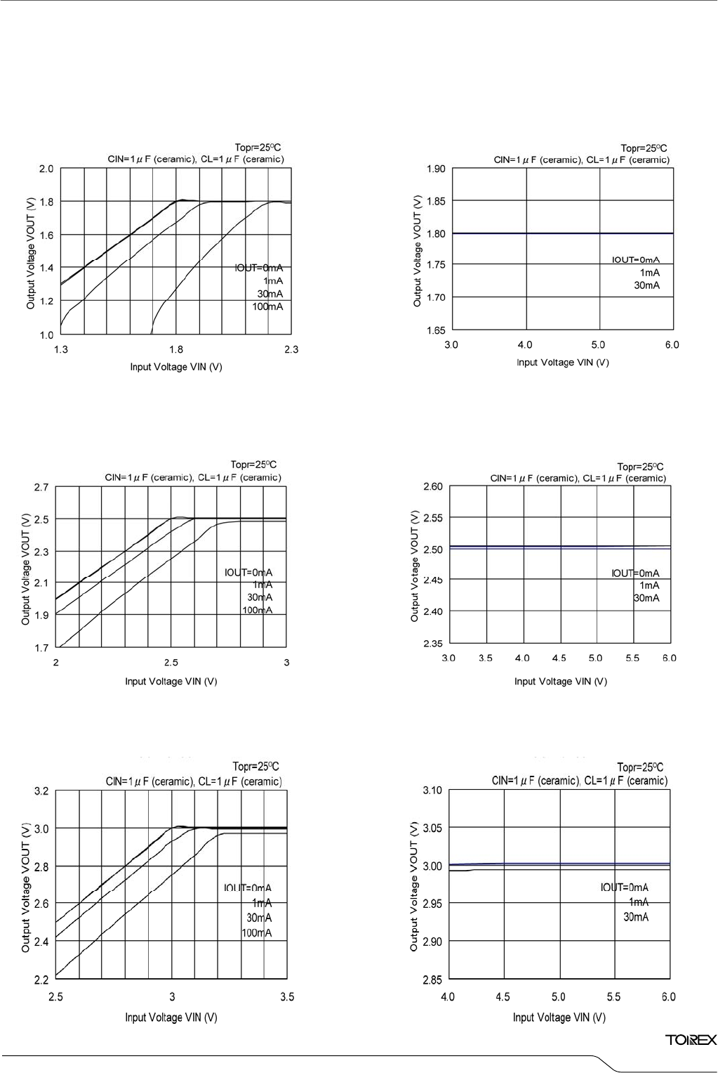
(2) Output Voltage vs. Input Voltage
■TYPICAL PERFORMANCE CHARACTERISTICS (Continued)
XC6219/11x182 XC6219/11x182
XC6219/11x252 XC6219/11x252
XC6219/11x302 XC6219/11x302
16/30
XC6219/XC6211 Series
■TYPICAL PERFORMANCE CHARACTERISTICS (Continued)
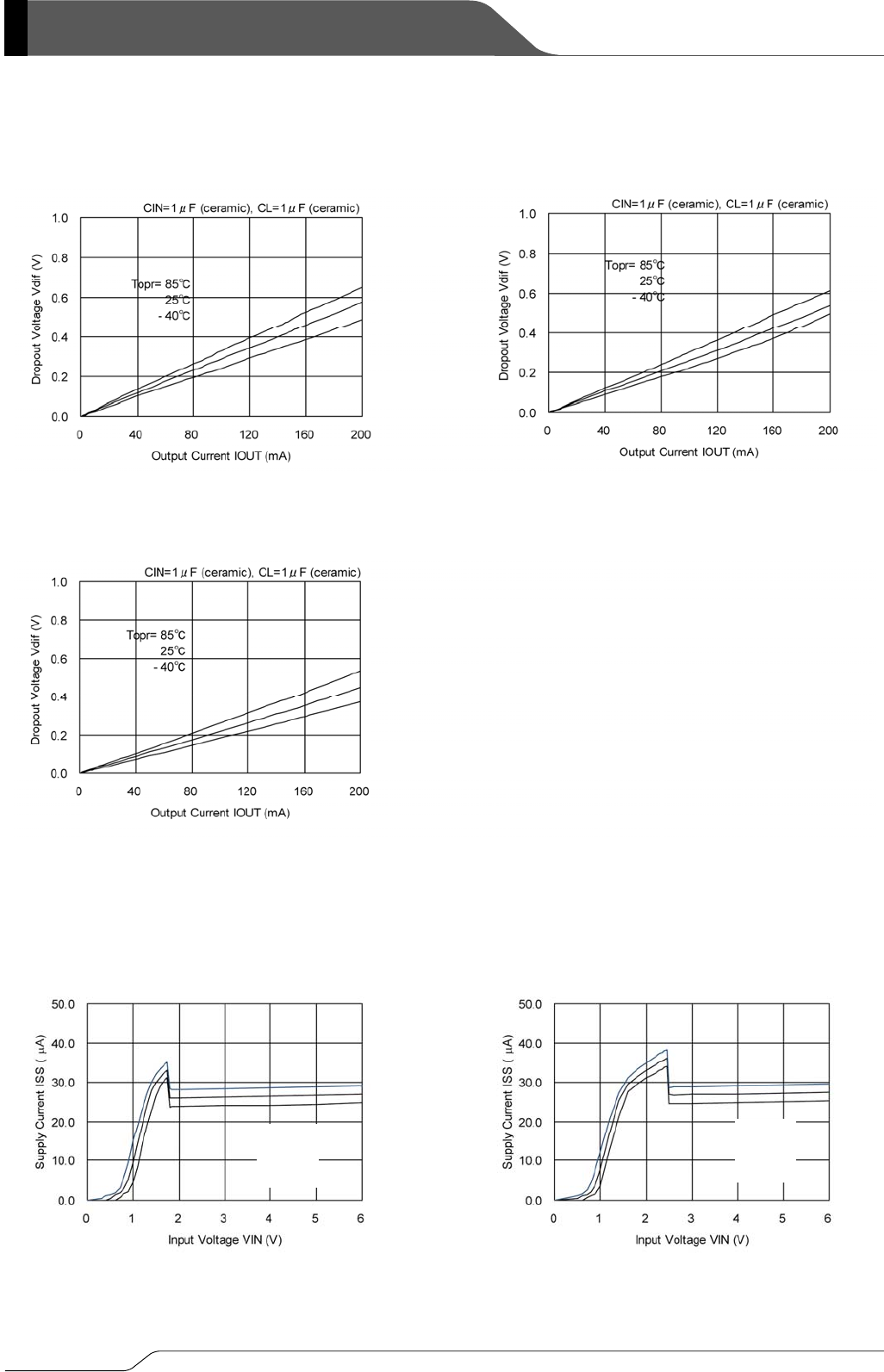
(3) Dropout Voltage vs. Output Current
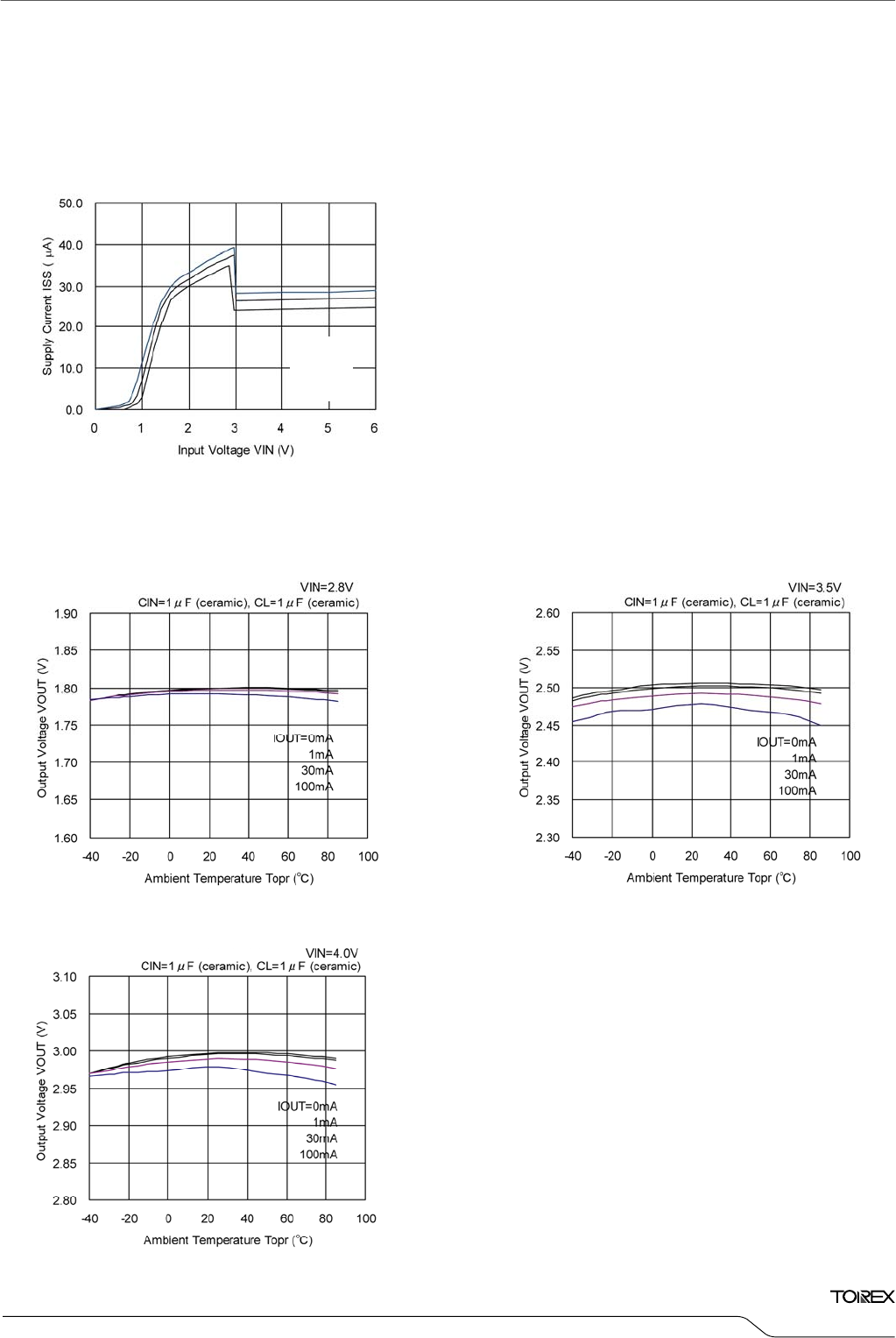
(4) Supply Current vs. Input Voltage
Topr = 85 ℃
25℃
-40℃
Topr = 85 ℃
25℃
-40℃
XC6219/11x182 XC6219/11x252
XC6219/11x302
XC6219/11x182 XC6219/11x252
17/30
XC6219/XC6211
Series
■TYPICAL PERFORMANCE CHARACTERISTICS (Continued)
(5) Output Voltage vs. Ambient Temperature
XC6219/11x182
X
C6219/11x252
XC6219/11x302
XC6219/11x302
Topr = 85 ℃
25℃
-40℃
(4) Supply Current vs. Input Voltage (Continued)
18/30
XC6219/XC6211 Series
■TYPICAL PERFORMANCE CHARACTERISTICS (Continued)
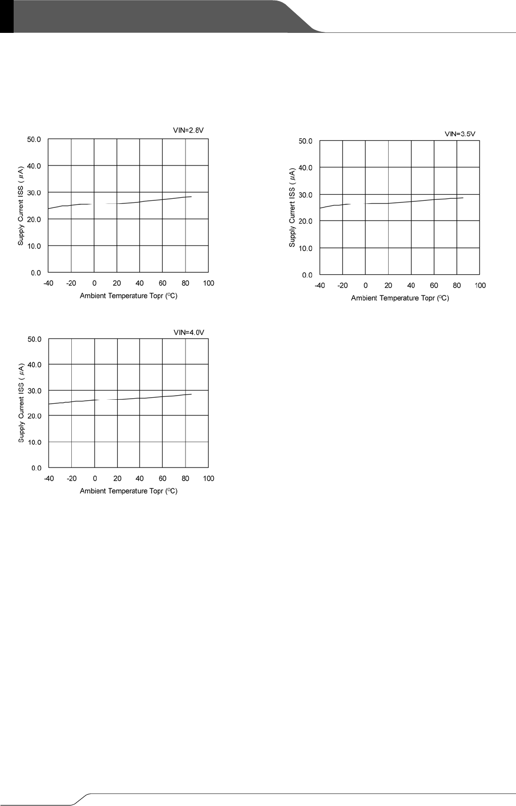
(6) Supply Current vs. Ambient Temperature
XC6219/11x182
XC6219/11x302
X
C6219/11x252
19/30
XC6219/XC6211
Series
■TYPICAL PERFORMANCE CHARACTERISTICS (Continued)
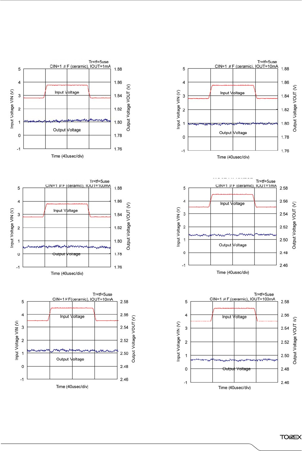
(7) Input Transient Response
XC6219/11x182
X
C6219/11x182
XC6219/11x182
X
C6219/11x252
XC6219/11x252
X
C6219/11x252
X
C6219/11x252
XC6219/11x252
X
C6219/11x252
20/30
XC6219/XC6211 Series
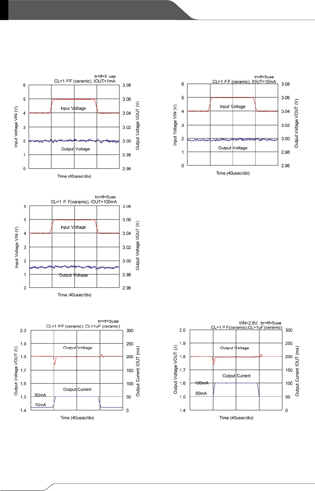
■TYPICAL PERFORMANCE CHARACTERISTICS (Continued)
(7) Input Transient Response (Continued)
(8) Load Transient Response
XC6219/11x302
X
C6219/11x302
X
C6219/11x302
XC6219/11x302
XC6219/11x182
X
C6219/11x182
21/30
XC6219/XC6211
Series
■TYPICAL PERFORMANCE CHARACTERISTICS (Continued)
(8) Load Transient Response (Continued)
XC6219/11x182
VIN=2.8V, trr=tf=5use
CL=1μF (ceramic), CL=1uF (ceramic)
XC6219/11x252
VIN=3.5V, trr=tf=5use
CL=1μF (ceramic), CL=1uF (ceramic)
XC6219/11x252
VIN=3.5V, trr=tf=5use
CL=1μF (ceramic), CL=1uF (ceramic)
XC6219/11x252
VIN=3.5V, trr=tf=5use
CL=1μF (ceramic), CL=1uF (ceramic)
XC6219/11x302
VIN=4.0V, trr=tf=5use
CL=1μF
(
ceramic
)
, CL=1uF
(
ceramic
)
XC6219/11x302
VIN=4.0V, trr=tf=5use
CL=1μF (ceramic), CL=1uF (ceramic)
22/30
XC6219/XC6211 Series
■TYPICAL PERFORMANCE CHARACTERISTICS (Continued)
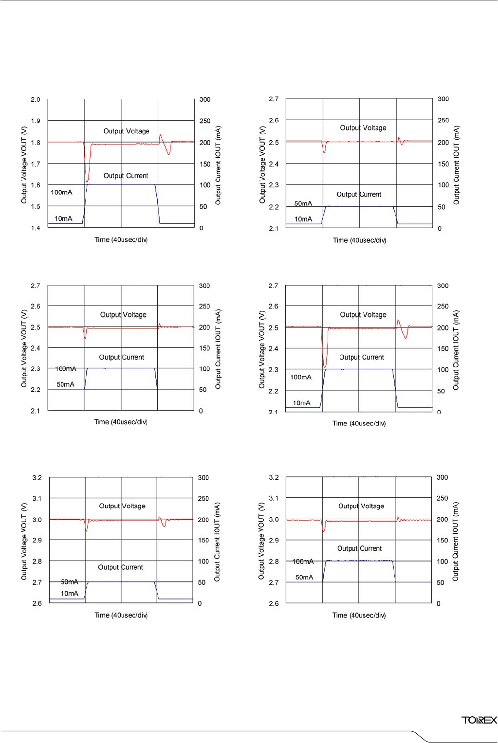
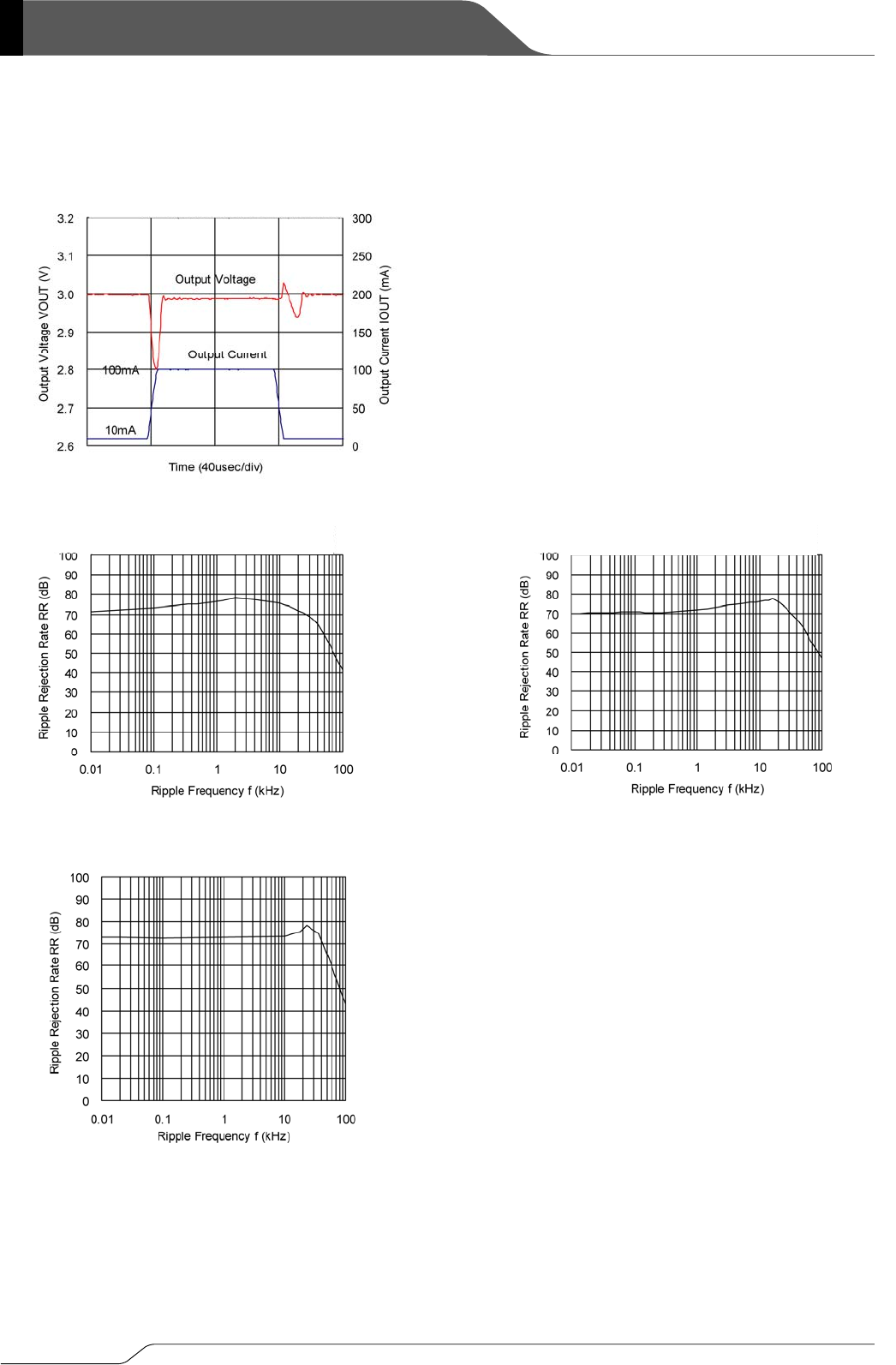
(8) Load Transient Response (Continued)
(9) Ripple Rejection Rate
XC6219/11
x
302
VIN=4.0V, trr=tf=5use
CL=1μF (ceramic), CL=1uF (ceramic)
XC6219/11
x
2
5
2
VIN=2.8V, DC+1Vp-pAC
IOUT=50mA, CL=1uF (ceramic)
XC6219/11x182
VIN=2.8V, DC+1Vp-pAC
IOUT=50mA, CL=1uF (ceramic)
XC6219/11
x
302
VIN=2.8V, DC+1Vp-pAC
IOUT=50mA, CL=1uF (ceramic)
23/30
XC6219/XC6211
Series
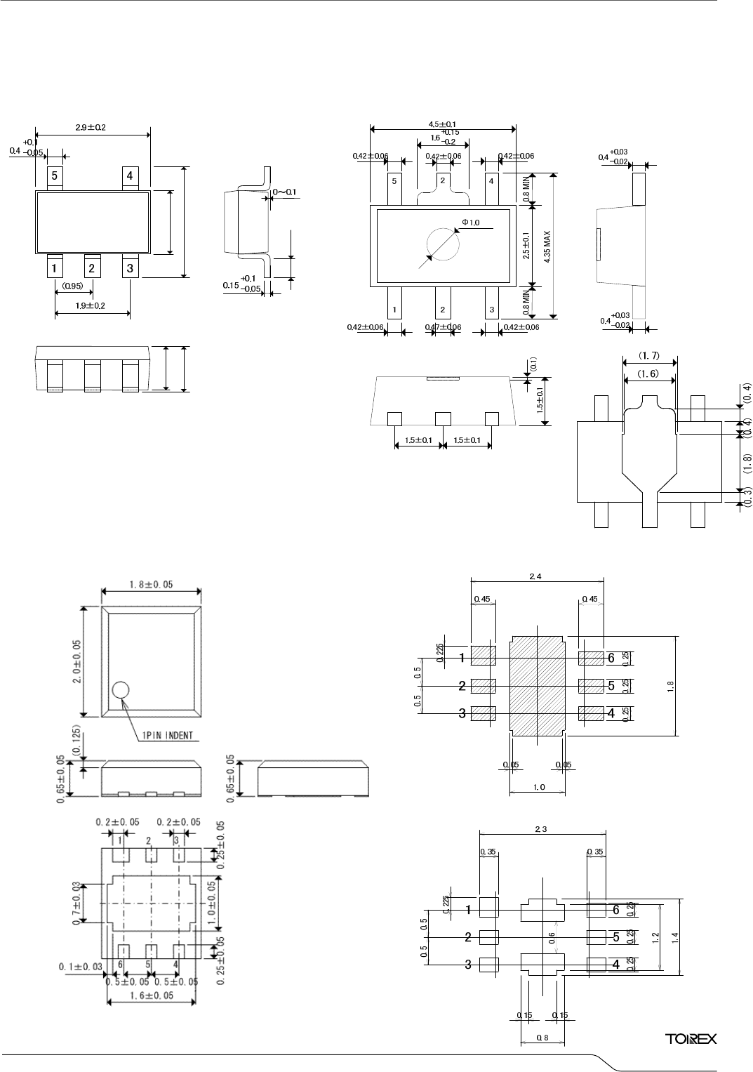
■PACKAGING INFORMATION
●SOT-25 ●SO
T
-89-5
●USP-6B
1.6 +0.2
-0.1
2.8±0.2
1.1±0.1
1.3MAX
0.2MIN
●USP-6B Reference Pattern Layout
●USP-6B Reference Metal Mask Design
24/30
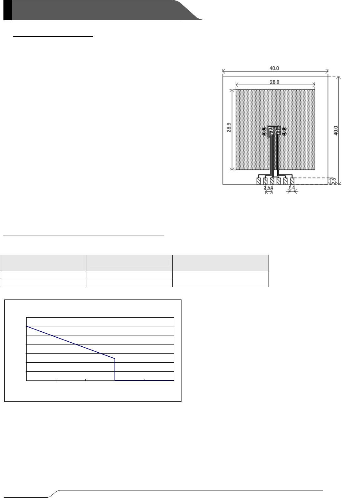
XC6219/XC6211 Series
● SOT-25 Power Dissipation
Power dissipation data for the SOT-25 is shown in this page.
The value of power dissipation varies with the mount board conditions.
Please use this data as the reference data taken in the following condition.
1. Measurement Condition
Condition: Mount on a board
Ambient: Natural convection
Soldering: Lead (Pb) free
Board Dimensions: 40 x 40 mm (1600 mm2 in one side)
Metal Area :
Copper (Cu) traces occupy 50% of the board
area in top and back faces.
Package heat-sink is tied to the copper traces
Material: Glass Epoxy (FR-4)
Thickness: 1.6 mm
Through-hole: 4 x 0.8 Diameter
2. Power Dissipation vs. Ambient Temperature(85℃)
Board Mount ( Tjmax=125℃)
Ambient Temperature (℃) Power Dissipation Pd (mW) Thermal Resistance (℃/W)
25 600
85 240
166.67
Evaluation Board (Unit: mm)
Pd vs Ta
0
100
200
300
400
500
600
700
25 45 65 85 105 125
Ambient Temperature Ta(℃)
Power Dissipation Pd(mW)
25/30
XC6219/XC6211
Series
● SOT-89-5 Power Dissipation
Power dissipation data for the SOT-89-5 is shown in this page.
The value of power dissipation varies with the mount board conditions.
Please use this data as the reference data taken in the following condition.
1. Measurement Condition
Condition: Mount on a board
Ambient: Natural convection
Soldering: Lead (Pb) free
Board Dimensions: 40 x 40 mm (1600 mm2 in one side)
Metal Area :
Copper (Cu) traces occupy 50% of the board
area in top and back faces.
Package heat-sink is tied to the copper traces
Material: Glass Epoxy (FR-4)
Thickness: 1.6 mm
Through-hole: 5 x 0.8 Diameter
Evaluation Board (Unit: mm)
2. Power Dissipation vs. Ambient Temperature(85℃)
Board Mount ( Tjmax=125℃)
Ambient Temperature (℃) Power Dissipation Pd (mW) Thermal Resistance (℃/W)
25 1300
85 520 76.92
28.9
40.0
2.5
Pd vs Ta
0
200
400
600
800
1000
1200
1400
25 45 65 85 105 125
Ambient Temperature Ta(℃)
Power Dissipation Pd(mW)
26/30
XC6219/XC6211 Series
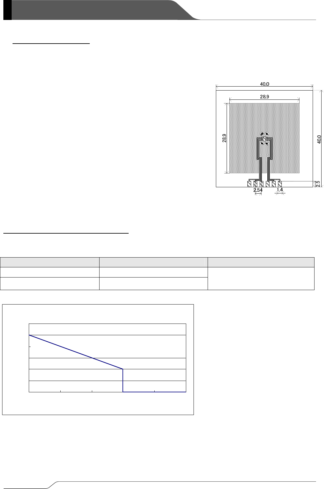
● USP-6B Power Dissipation
Power dissipation data for the USP-6B is shown in this page.
The value of power dissipation varies with the mount board conditions.
Please use this data as the reference data taken in the following condition.
1. Measurement Condition
Condition: Mount on a board
Ambient: Natural convection
Soldering: Lead (Pb) free
Board Dimensions: 40 x 40 mm (1600 mm2 in one side)
Metal Area: Copper (Cu) traces occupy 50% of the board
area in top and back faces.
Package heat-sink is tied to the copper traces
Material: Glass Epoxy (FR-4)
Thickness: 1.6 mm
Through-hole: 4 x 0.8 Diameter
2. Power Dissipation vs. Ambient Temperature
Board Mount (Tj max = 125℃)
Ambient Temperature(℃) Power Dissipation Pd(mW) Thermal Resistance(℃/W)
25 1000
85 400
100.00
Evaluation Board (Unit: mm)
Pd vs Ta
0
200
400
600
800
1000
1200
25 45 65 85 105 125
Ambient Temperature Ta(℃)
Power Dissipation Pd(mW)
27/30
XC6219/XC6211
Series
MARK
VOUT 100mV INCREMENTS VOUT 50mV INCREMENTS
VOUT:0.1~3.0V VOUT:3.1~6.0V VOUT:0.15~3.05V VOUT:3.15~6.05V
PRODUCT SERIES
V A E L XC6219Axxxxx
X B F M XC6219Bxxxxx
Y C H N XC6219Cxxxxx
Z D K P XC6219Dxxxxx
V A E L XC6219Exxxxx
X B F M XC6219Fxxxxx
Y C H N XC6219Gxxxxx
Z D K P XC6219Hxxxxx
MARK OUTPUT VOLTAGE (V) MARK OUTPUT VOLTAGE (V)
0 - 3.1 - 3.15 F 1.6 4.6 1.65 4.65
1 - 3.2 - 3.25 H 1.7 4.7 1.75 4.75
2 - 3.3 - 3.35 K 1.8 4.8 1.85 4.85
3 - 3.4 - 3.45 L 1.9 4.9 1.95 4.95
4 - 3.5 - 3.55 M 2.0 5.0 2.05 -
5 - 3.6 - 3.65 N 2.1 - 2.15 -
6 - 3.7 - 3.75 P 2.2 - 2.25 -
7 - 3.8 - 3.85 R 2.3 - 2.35 -
8 0.9 3.9 0.95 3.95 S 2.4 - 2.45 -
9 1.0 4.0 1.05 4.05 T 2.5 - 2.55 -
A 1.1 4.1 1.15 4.15 U 2.6 - 2.65 -
B 1.2 4.2 1.25 4.25 V 2.7 - 2.75 -
C 1.3 4.3 1.35 4.35 X 2.8 - 2.85 -
D 1.4 4.4 1.45 4.45 Y 2.9 - 2.95 -
E 1.5 4.5 1.55 4.55 Z 3.0 - 3.05 -
MARK PRODUCT SERIES
L XC6219xxxxxx
① represents product series
② represents type of regulator
④ represents production lot number
0 to 9, A to Z reverse character of 0 to 9, A to Z repeated (G, I, J, O, Q, W excluded)
③ represents output voltage
■MARKING RULE
[XC6219 Series]
●SOT-25, SOT-89-5
① ② ③ ④
123
54
SOT-25
(TOP VIEW)
524
④③
②①
123
SOT-89-5
(TOP VIEW)
28/30
XC6219/XC6211 Series
MARK
① ② PRODUCT SERIES
1 9 XC6219xxxxDx
MARK TYPE PRODUCT SERIES
A High Active, pull-down resistor built-in (semi-custom) XC6219AxxxMx
B High Active, no pull-down resistor built-in (standard) XC6219BxxxMx
C Low Active, pull-up resistor built-in (semi-custom) XC6219CxxxMx
D Low Active, no pull-up resistor built-in (semi-custom) XC6219DxxxMx
E High Active, pull-down resistor built-in (semi-custom) XC6219ExxxDx
F High Active, no pull-down resistor built-in (standard) XC6219FxxxDx
Z Low Active, pull-up resistor built-in (semi-custom) XC6219GxxxDx
H Low Active, no pull-up resistor built-in (semi-custom) XC6219HxxxDx
MARK VOLTAGE (V) PRODUCT SERIES
3 3.X XC6219x3xxDx
5 5.X XC6219x5xxDx
MARK VOLTAGE PRODUCT SERIES SYMBOL VOLTAGE PRODUCT SERIES
0 X.0 XC6219xx0xDx A X.05 XC6219xx0ADx
1 X.1 XC6219xx1xDx B X.15 XC6219xx1ADx
2 X.2 XC6219xx2xDx C X.25 XC6219xx2ADx
3 X.3 XC6219xx3xDx D X.35 XC6219xx3ADx
4 X.4 XC6219xx4xDx E X.45 XC6219xx4ADx
5 X.5 XC6219xx5xDx F X.55 XC6219xx5ADx
6 X.6 XC6219xx6xDx H X.65 XC6219xx6ADx
7 X.7 XC6219xx7xDx K X.75 XC6219xx7ADx
8 X.8 XC6219xx8xDx L X.85 XC6219xx8ADx
9 X.9 XC6219xx9xDx M X.95 XC6219xx9ADx
①② represents product series
③ represents type of regulator
⑥ represents production lot number
0 to 9, A to Z repeated (
G, I, J, O, Q, W
excluded)
* No character inversion used.
⑤ represents output voltage
④ represents product series
■MARKING RULE (Continued)
●USP-6B
USP-6B
(TOP VIEW)
29/30
XC6219/XC6211
Series
MARK
VOUT 100mV INCREMENTS VOUT 50mV INCREMENTS
VOUT:0.1~3.0V VOUT:3.1~6.0V VOUT:0.15~3.05V VOUT:3.15~6.05V
PRODUCT SERIES
V A E L XC6211AxxxMx
X B F M XC6211BxxxMx
Y C H N XC6211CxxxMx
Z D K P XC6211DxxxMx
V A E L XC6211ExxxMx
X B F M XC6211FxxxMx
Y C H N XC6211GxxxMx
Z D K P XC6211HxxxMx
MARK OUTPUT VOLTAGE (V) MARK OUTPUT VOLTAGE (V)
0 - 3.1 - 3.15 F 1.6 4.6 1.65 4.65
1 - 3.2 - 3.25 H 1.7 4.7 1.75 4.75
2 - 3.3 - 3.35 K 1.8 4.8 1.85 4.85
3 - 3.4 - 3.45 L 1.9 4.9 1.95 4.95
4 - 3.5 - 3.55 M 2.0 5.0 2.05 5.05
5 - 3.6 - 3.65 N 2.1 5.1 2.15 5.15
6 - 3.7 - 3.75 P 2.2 5.2 2.25 5.25
7 - 3.8 - 3.85 R 2.3 5.3 2.35 5.35
8 - 3.9 - 3.95 S 2.4 5.4 2.45 5.45
9 - 4.0 - 4.05 T 2.5 5.5 2.55 5.55
A - 4.1 - 4.15 U 2.6 5.6 2.65 5.65
B - 4.2 - 4.25 V 2.7 5.7 2.75 5.75
C - 4.3 - 4.35 X 2.8 5.8 2.85 5.85
D - 4.4 - 4.45 Y 2.9 5.9 2.95 5.95
E - 4.5 - 4.55 Z 3.0 6.0 3.05 6.05
MARK PRODUCT SERIES
A XC6211xxxxMx
■MARKING RULE (Continued)
① represents product series
② represents type of regulator
④ represents production lot number
0 to 9, A to Z reverse character of 0 to 9, A to Z repeated (G, I, J, O, Q, W excluded)
③ represents output voltage
[XC6211 Series]
●SOT-25
① ② ③ ④
123
54
30/30
XC6219/XC6211 Series
1. The products and product specifications contained herein are subject to change without
notice to improve performance characteristics. Consult us, or our representatives
before use, to confirm that the information in this datasheet is up to date.
2. We assume no responsibility for any infringement of patents, patent rights, or other
rights arising from the use of any information and circuitry in this datasheet.
3. Please ensure suitable shipping controls (including fail-safe designs and aging
protection) are in force for equipment employing products listed in this datasheet.
4. The products in this datasheet are not developed, designed, or approved for use with
such equipment whose failure of malfunction can be reasonably expected to directly
endanger the life of, or cause significant injury to, the user.
(e.g. Atomic energy; aerospace; transport; combustion and associated safety
equipment thereof.)
5. Please use the products listed in this datasheet within the specified ranges.
Should you wish to use the products under conditions exceeding the specifications,
please consult us or our representatives.
6. We assume no responsibility for damage or loss due to abnormal use.
7. All rights reserved. No part of this datasheet may be copied or reproduced without the
prior permission of TOREX SEMICONDUCTOR LTD.