X Powers AC101 User Manual V1.1
x-powers%20AC101%20User%20Manual%20v1.1
x-powers%20AC101%20User%20Manual%20v1.1
x-powers%20AC101%20User%20Manual%20v1.1
User Manual:
Open the PDF directly: View PDF ![]() .
.
Page Count: 70
- Declaration
- About Documentation
- Revision History
- Table of Contents
- Description
- Features
- Applications
- Functional Block Diagram
- Pin Assignment
- Package Dimension
- Pin/Signal Description
- Electrical Characteristics
- Analog Performance Characteristics
- Typical Power Consumption
- Function Description
- Register List
- Reg 00h_Chip Soft Reset Register
- Reg 01h_PLL Configure Control 1 Register
- Reg 02h_PLL Configure Control 2 Register
- Reg 03h_System Clocking Control Register
- Reg 04h_Module Clock Enable Control Register
- Reg 05h_Module Reset Control Register
- Reg 06h_ADDA Sample Rate Configuration Register
- Reg 10h_I2S1 BCLK/LRCK Control Register
- Reg 11h_I2S1 SDOUT Control Register
- Reg 12h_I2S1 SDIN Control Register
- Reg 13h_I2S1 Digital Mixer Source Select Register
- Reg 14h_I2S1 Volume Control 1 Register
- Reg 15h_I2S1 Volume Control 2 Register
- Reg 16h_I2S1 Volume Control 3 Register
- Reg 17h_I2S1 Volume Control 4 Register
- Reg 18h_I2S1 Digital Mixer Gain Control Register
- Reg 40h_ADC Digital Control Register
- Reg 41h_ADC Volume Control Register
- Reg 44h_HMIC Control 1 Register
- Reg 45h_HMIC Control 2 Register
- Reg 46h_HMIC Status Register
- Reg 48h_DAC Digital Control Register
- Reg 49h_DAC Volume Control Register
- Reg 4ch_DAC Digital Mixer Source Select Register
- Reg 4dh_DAC Digital Mixer Gain Control Register
- Reg 50h_ADC Analog Control Register
- Reg 51h_ADC Source Select Register
- Reg 52h_ADC Source Boost Control Register
- Reg 53h_Output Mixer & DAC Analog Control Register
- Reg 54h_Output Mixer Source Select Register
- Reg 55h_Output Mixer Source Boost Register
- Reg 56h_Headphone Output Control Register
- Reg 58h_Speaker Output Control Register
- Reg a0h_DAC DAP Control Register
- Reg a1h_DAC DAP High HPF Coef Register
- Reg a2h_DAC DAP Low HPF Coef Register
- Reg a3h_DAC DAP Left High Energy Average Coef Regi
- Reg a4h_DAC DAP Left Low Energy Average Coef Regis
- Reg a5h_DAC DAP Right High Energy Average Coef Reg
- Reg a6h_DAC DAP Right Low Energy Average Coef Regi
- Reg a7h_DAC DAP High Gain Decay Time Coef Register
- Reg a8h_DAC DAP Low Gain Decay Time Coef Register
- Reg a9h_DAC DAP High Gain Attack Time Coef Registe
- Reg aah_DAC DAP Low Gain Attack Time Coef Register
- Reg abh_DAC DAP High Energy Threshold Register
- Reg ach_DAC DAP Low Energy Threshold Register
- Reg adh_DAC DAP High Gain K Parameter Register
- Reg aeh_DAC DAP Low Gain K Parameter Register
- Reg afh_DAC DAP High Gain Offset Parameter Registe
- Reg b0h_DAC DAP Low Gain Offset Parameter Register
- Reg b1h _DAC DAP Optimum Register
- Reg b5h_DAC DAP Enable Register

AC101
User Manual
Revision 1.1
2015/1/11
Copyright©2014 X-Powers Technology. All Rights Reserved.

Declaration
This documentation is the original work and copyrighted property of X-Powers. Reproduction in whole or
in part must obtain the written approval of X-Powers and give clear acknowledgement to the copyright
owner.
The information furnished by X-Powers is believed to be accurate and reliable. X-Powers reserves the right
to make changes in circuit design and/or specifications at any time without notice. X-Powers does not
assume any responsibility and liability for its use. Nor for any infringements of patents or other rights of the
third parties which may result from its use. No license is granted by implication or otherwise under any
patent or patent rights of X-Powers. This documentation neither states nor implies warranty of any kind,
including fitness for any particular application.
Third party licences may be required to implement the solution/product. Customers shall be solely
responsible to obtain all appropriately required third party licences. X-Powers shall not be liable for any
licence fee or royalty due in respect of any required third party licence. X-Powers shall have no warranty,
indemnity or other obligations with respect to matters covered under any required third party licence.

About Documentation
This documentation of AC101 is intended to be used by board-level product designers and product software
developers. The manual assumes that the reader has a background in computer engineering and/or software
engineering and understands concepts of digital system design, microprocessor architecture, Input / Output
(I/O) devices, industry standard communication and device interface protocols.
Organization
This document aims to describe the AC101 from following aspects: block diagram, pin assignment,
pin/signal description, electrical characteristics, typical application, system description and register
description.

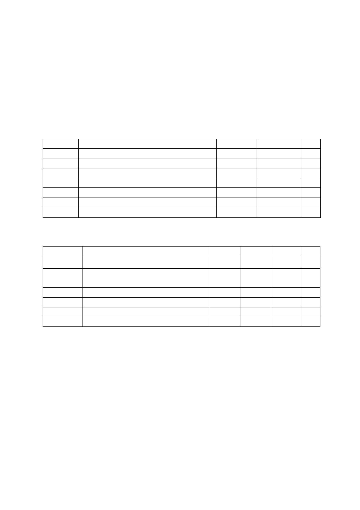
Revision History
Version
Date
Description
V1.0
2014/12/1
Completed Draft
V1.1
2015/1/11

Table of Contents
Declaration......................................................................................................................................................... 2
About Documentation........................................................................................................................................3
Revision History................................................................................................................................................ 4
Table of Contents............................................................................................................................................... 5
1. Description..................................................................................................................................................... 9
2. Features........................................................................................................................................................ 10
3. Applications................................................................................................................................................. 11
4. Functional Block Diagram...........................................................................................................................11
4.1. Functional Block Diagram................................................................................................................11
4.2. Data Path Diagram............................................................................................................................12
5. Pin Assignment............................................................................................................................................ 13
6. Package Dimension......................................................................................................................................14
7. Pin/Signal Description................................................................................................................................. 15
8. Electrical Characteristics............................................................................................................................. 17
8.1. Absolute Maximum Ratings.............................................................................................................17
8.2. Recommended Operating Conditions...............................................................................................17
8.3. Static Characteristics........................................................................................................................ 18
9. Analog Performance Characteristics........................................................................................................... 19
10. Typical Power Consumption......................................................................................................................21
11. Function Description..................................................................................................................................22
11.1. Power.............................................................................................................................................. 22
11.2. Clock............................................................................................................................................... 23
11.3. PLL................................................................................................................................................. 24
11.4. TWI/RSB Interface.........................................................................................................................25

11.4.1. TWI Interface.......................................................................................................................25
11.4.2. RSB Interface.......................................................................................................................26
11.5. I2S/PCM Interface.......................................................................................................................... 28
11.6. Stereo ADC..................................................................................................................................... 32
11.7. Stereo DAC.....................................................................................................................................32
11.8. Mixer...............................................................................................................................................32
11.8.1. DAC Output Mixers............................................................................................................ 32
11.8.2. ADC Record Mixers............................................................................................................32
11.8.3. Digital Mixers......................................................................................................................33
11.9. Analogue Audio Input Path............................................................................................................ 34
11.9.1. Microphone Input................................................................................................................ 34
11.9.2. LINEINL/R Input................................................................................................................ 34
11.10. Analogue Audio Output Path........................................................................................................35
11.10.1. Headphone Output.............................................................................................................35
11.10.2. Speaker Output.................................................................................................................. 35
11.11. Digital Microphone Interface....................................................................................................... 37
11.12. Audio Jack Detect.........................................................................................................................38
11.13. Interrupt.........................................................................................................................................39
11.14. Digital Audio Process for DAC....................................................................................................40
11.14.1. High Pass Filter..................................................................................................................41
11.14.2. Dynamic Range Control.................................................................................................... 41
12. Register List............................................................................................................................................... 44
Reg 00h_Chip Soft Reset Register.......................................................................................................... 45
Reg 01h_PLL Configure Control 1 Register...........................................................................................45
Reg 02h_PLL Configure Control 2 Register...........................................................................................46
Reg 03h_System Clocking Control Register...........................................................................................46

Reg 04h_Module Clock Enable Control Register...................................................................................47
Reg 05h_Module Reset Control Register................................................................................................47
Reg 06h_ADDA Sample Rate Configuration Register........................................................................... 48
Reg 10h_I2S1 BCLK/LRCK Control Register....................................................................................... 48
Reg 11h_I2S1 SDOUT Control Register................................................................................................ 50
Reg 12h_I2S1 SDIN Control Register.................................................................................................... 51
Reg 13h_I2S1 Digital Mixer Source Select Register..............................................................................52
Reg 14h_I2S1 Volume Control 1 Register.............................................................................................. 53
Reg 15h_I2S1 Volume Control 2 Register.............................................................................................. 53
Reg 16h_I2S1 Volume Control 3 Register.............................................................................................. 54
Reg 17h_I2S1 Volume Control 4 Register.............................................................................................. 54
Reg 18h_I2S1 Digital Mixer Gain Control Register...............................................................................55
Reg 40h_ADC Digital Control Register..................................................................................................56
Reg 41h_ADC Volume Control Register................................................................................................ 56
Reg 44h_HMIC Control 1 Register.........................................................................................................57
Reg 45h_HMIC Control 2 Register.........................................................................................................57
Reg 46h_HMIC Status Register.............................................................................................................. 58
Reg 48h_DAC Digital Control Register..................................................................................................59
Reg 49h_DAC Volume Control Register................................................................................................ 59
Reg 4ch_DAC Digital Mixer Source Select Register............................................................................. 60
Reg 4dh_DAC Digital Mixer Gain Control Register..............................................................................60
Reg 50h_ADC Analog Control Register................................................................................................. 61
Reg 51h_ADC Source Select Register.................................................................................................... 61
Reg 52h_ADC Source Boost Control Register....................................................................................... 62
Reg 53h_Output Mixer & DAC Analog Control Register......................................................................63
Reg 54h_Output Mixer Source Select Register.......................................................................................63

Reg 55h_Output Mixer Source Boost Register.......................................................................................64
Reg 56h_Headphone Output Control Register........................................................................................64
Reg 58h_Speaker Output Control Register............................................................................................. 65
Reg a0h_DAC DAP Control Register..................................................................................................... 66
Reg a1h_DAC DAP High HPF Coef Register........................................................................................ 66
Reg a2h_DAC DAP Low HPF Coef Register.........................................................................................66
Reg a3h_DAC DAP Left High Energy Average Coef Register.............................................................. 66
Reg a4h_DAC DAP Left Low Energy Average Coef Register...............................................................67
Reg a5h_DAC DAP Right High Energy Average Coef Register............................................................67
Reg a6h_DAC DAP Right Low Energy Average Coef Register............................................................ 67
Reg a7h_DAC DAP High Gain Decay Time Coef Register................................................................... 67
Reg a8h_DAC DAP Low Gain Decay Time Coef Register....................................................................67
Reg a9h_DAC DAP High Gain Attack Time Coef Register...................................................................67
Reg aah_DAC DAP Low Gain Attack Time Coef Register....................................................................68
Reg abh_DAC DAP High Energy Threshold Register........................................................................... 68
Reg ach_DAC DAP Low Energy Threshold Register............................................................................ 68
Reg adh_DAC DAP High Gain K Parameter Register........................................................................... 68
Reg aeh_DAC DAP Low Gain K Parameter Register............................................................................ 68
Reg afh_DAC DAP High Gain Offset Parameter Register.....................................................................68
Reg b0h_DAC DAP Low Gain Offset Parameter Register.....................................................................69
Reg b1h _DAC DAP Optimum Register.................................................................................................69
Reg b5h_DAC DAP Enable Register...................................................................................................... 69

1. Description
The AC101 is a highly integrated audio codec designed for player and tablet application platforms. It has
one I2S/PCM interface, 2 channel DAC and 2 channel ADC with a high level of mixed-signal integration.
An integrated digital PLL supports a large range of input/output frequencies, and It can generate required
audio clocks for codec from standard audio crystal rate such as 22.5792MHz and 24.576MHz, also can be
from common reference clock frequencies such as 12MHz, 13MHz and 19.2MHz, and an internal RC
oscillator can be used in Free-running Mode, where the application processor can be inactive during voice
call application. The 2 ADC and 2 DAC in device use advanced multi-bit delta-sigma modulation technique
to convert data between analog and digital . The SNR performance can reach 100 dB A-wight.
Three analog input paths allow diverse analog audio sources such as two sets of differential microphone,
one differential or single-ended linein or stereo FM input.
One ground-reference headphone output is provided. The output amplifier are powered from an integrated
Charge Pump in order to achieve a higher quality, less power consumption in headphone playback, whist
without any DC blocking capacitor and avoiding unwanted noise.
Two stereo differential speaker output is available by using an external amplifier to drive the loud-speaker.
It can also be configured as single-ended output pin for some application of external single-ended amplifier.
The flexible analogue and digital mixers form a varied signal routing to support a complicated application.
AC101 is controlled through TWI (2-wire serial interface ) or RSB①(reduced serial bus) . It works only in
the slave mode .
The integrated DRC(Dynamic Range Controller) function in AC101 provide an useful digital sound
processing capability in DAC playback path to speaker . It is uesed to attenuate the peak signals and boost
the low-level signals by adjusting the output signal gain in some conditions. The DRC functions can be
enable or disable in the playback path .
The integrated AGC(Automatic Gain Controller) function can be used to maintain a constant recording
level in ADC record path . The DRC can make an improvement in background noise by setting a
programmable Noise Gate to attenuate very low-level input signals .
Note: ①The RSB is independent R&D by x-powers, supports a special protocols with a simplified two wire protocol on a push-pull bus. The
transfer speed in AC101 can be up to 10MHz .

2. Features
The AC101 features:
• 2 ADCs and 2 DACs @ 24-bit and inter PLL processing with flexible clocking scheme
• Up to 100dB SNR during DAC playback path (A ' weight)
• Up to 95dB SNR during ADC record path (A ' weight)
• Capless stereo headphone driver
–Integrated charge pump for 0V reference
–18mW @1.8V
• Two stereo differential speaker outputs using external amplifier to drive the loud speaker
• Three audio inputs
–Two differential analog microphone inputs with 30dB~48dB boost amplifier gain
–One mono differential or single-ended line-in input
• Two low noise analog microphone bias
• Audio jack insert/ button press detection
• TWI/RSB control interface
• 24-bit 8KHz ~ 192KHz I2S/PCM interface
• Support Dynamic Range Controller (DRC) adjusting the DAC playback output
• Support Automatic Gain Control (AGC) adjusting the ADC recording output
• SRC for synchronisation between audio interface or digital audio data mixing
• Soft mute circuit for pop noise suppression
• Support one stereo digital microphone interface
• QFN 40-pin package, 5mm x 5mm
3. Applications
• Tablets
• Box/Player
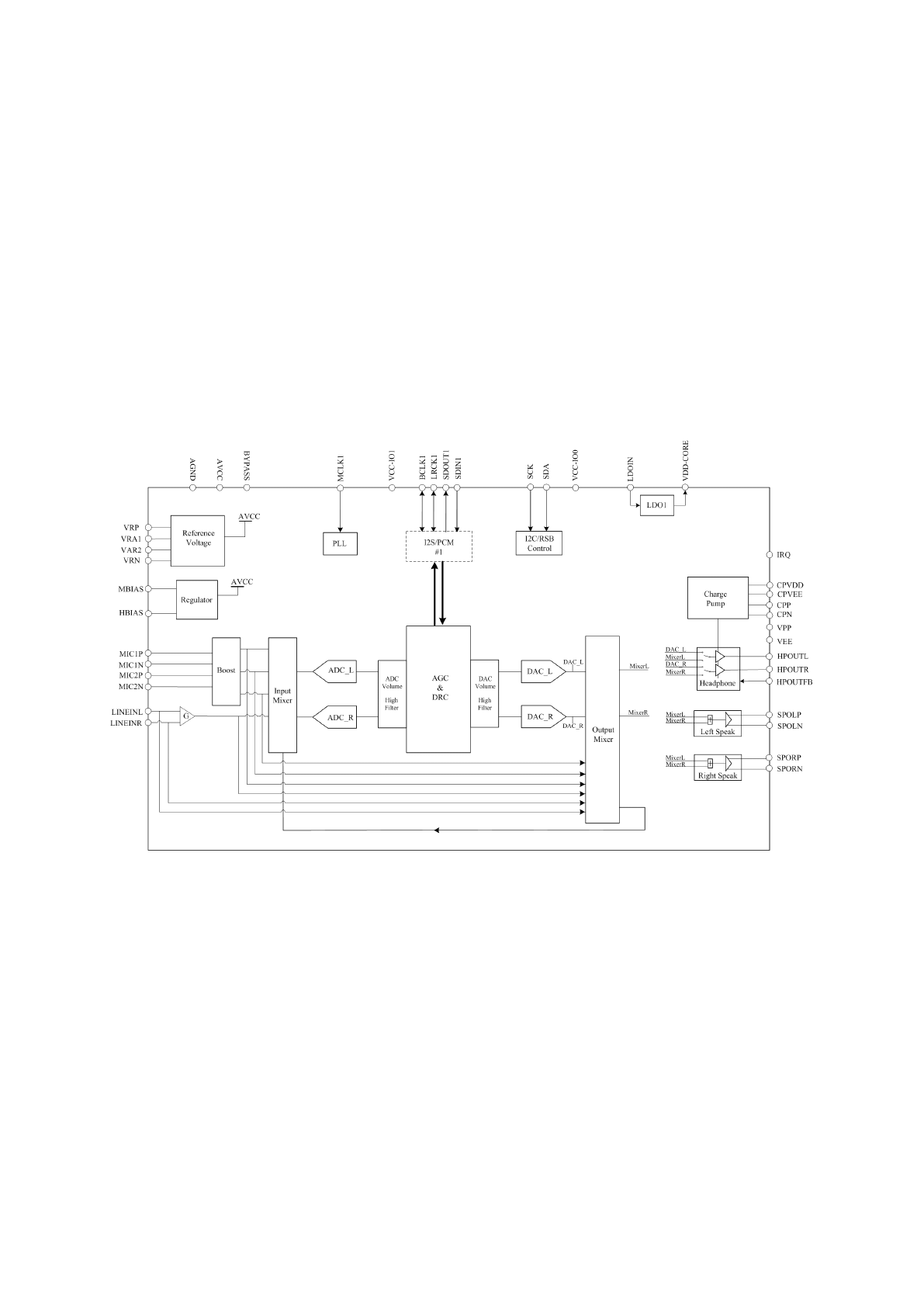
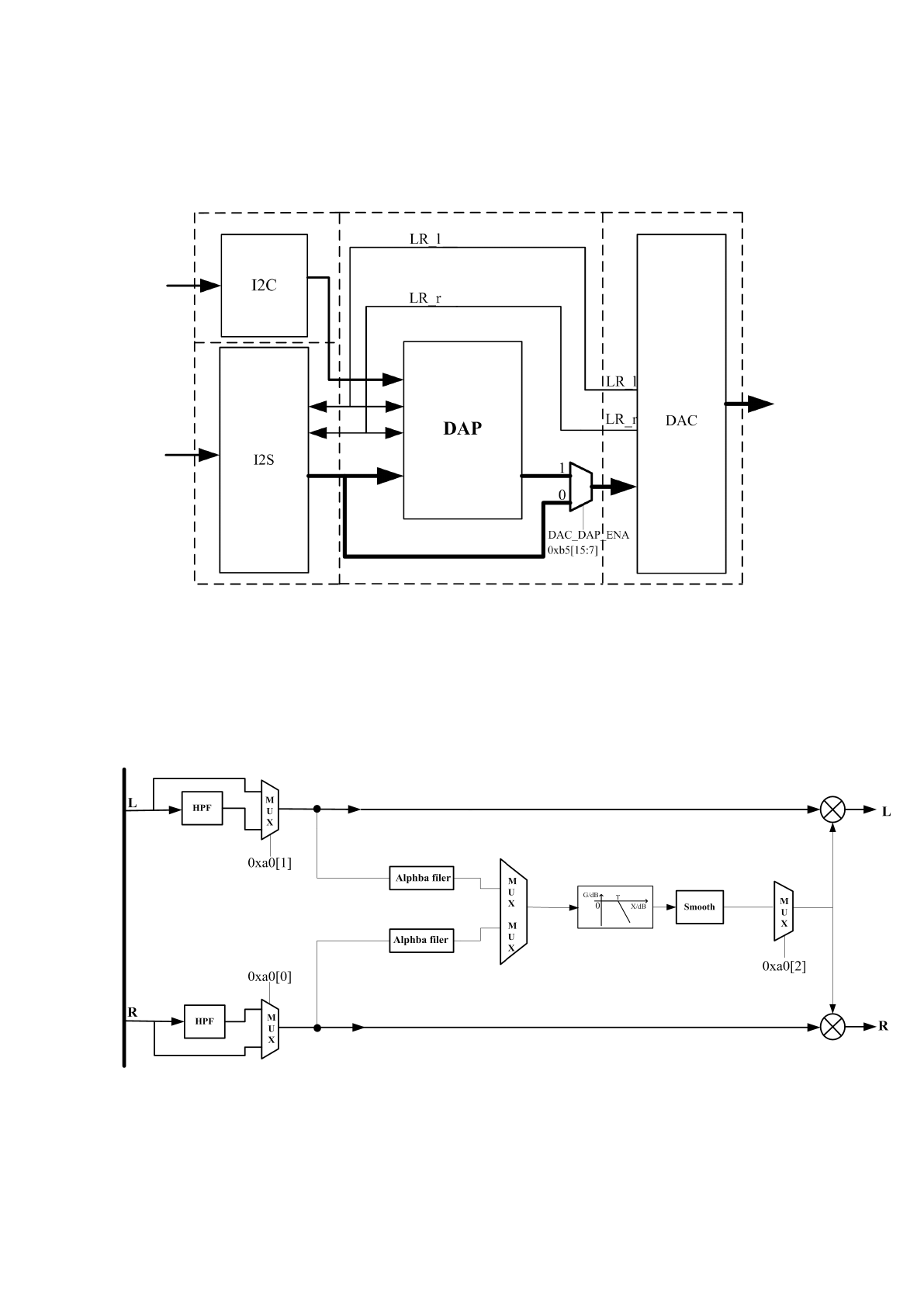
4. Functional Block Diagram
4.1. Functional Block Diagram
Figure 1 Functional Block Diagram
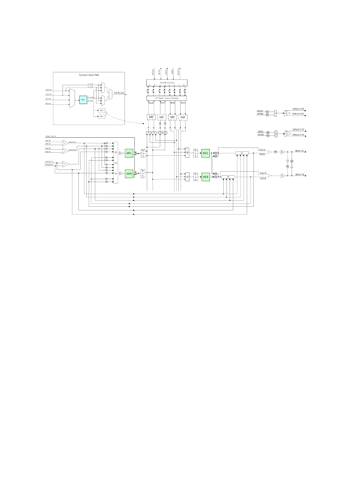
4.2. Data Path Diagram
Figure 2 Data Path Diagram
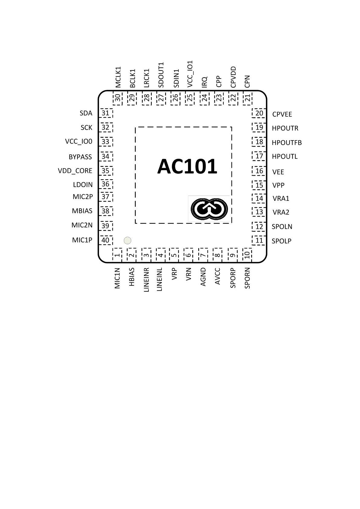
5. Pin Assignment
Figure 3 Pin Assignment
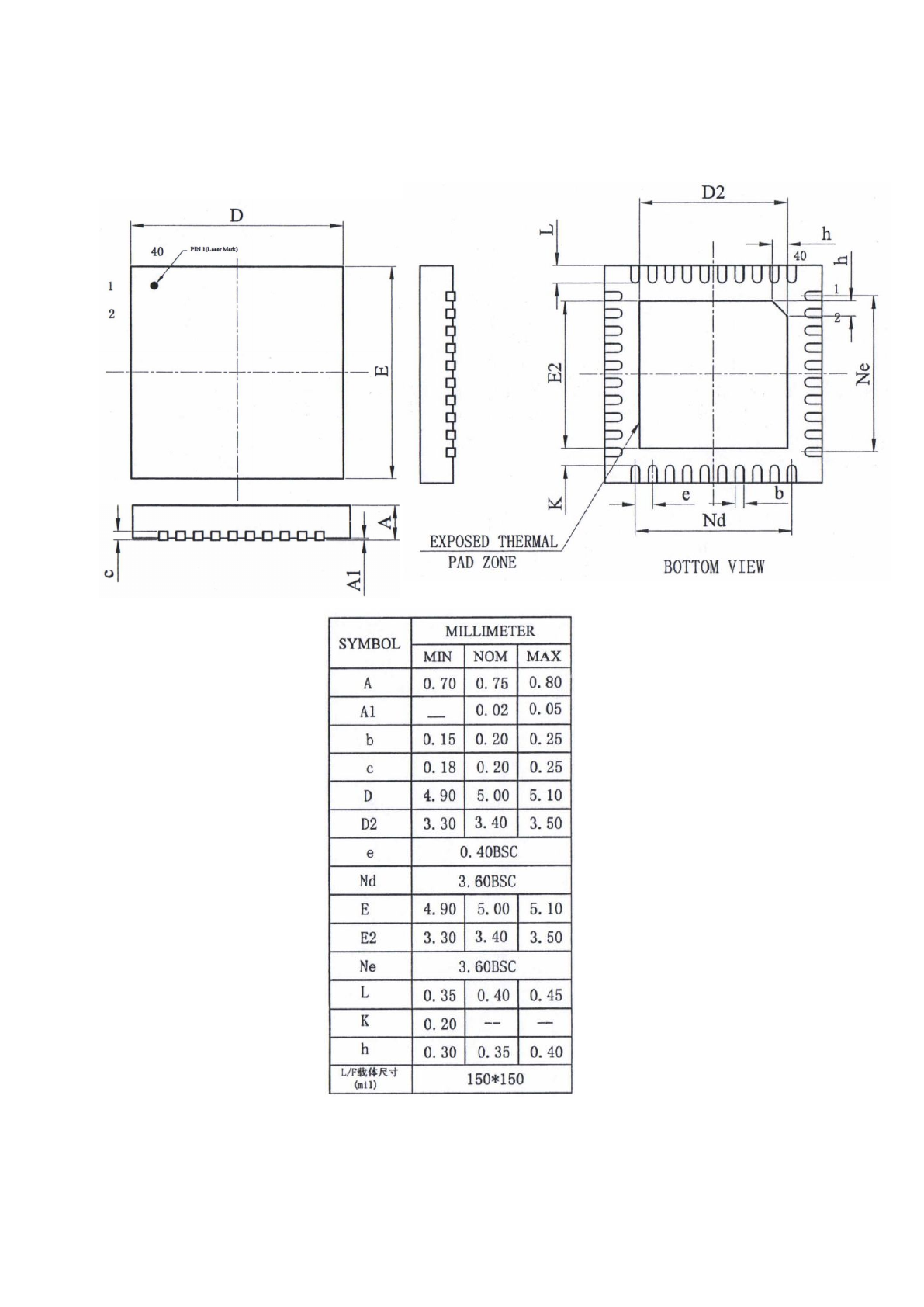
6. Package Dimension
Figure 4 Package Dimension

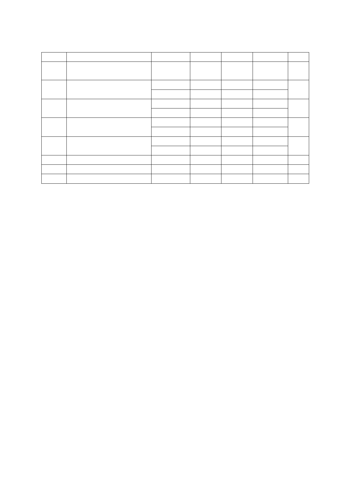
7. Pin/Signal Description
This chapter describes the 68 pins of AC101 from four aspects: pin number, signal name, type, and pin
definition. All the pins are classified into four groups, including digital IO pin, analog IO pin,
filter/reference, and power/ground.
There are five pin types here: O for output, I for input, I/O for input/output, P for power, and G for ground.
Pin Number
Signal Name
Type
Description
Digital IO Pins
30
MCLK1
I
I2S interface master input clock
26
SDIN1
I
I2S interface serial data input
27
SDOUT1
O
I2S interface serial data output
29
BCLK1
I/O
I2S interface serial bit clock
28
LRCK1
I/O
I2S interface synchronous clock
31
SDA
I/O
TWI interface serial data(Open-drain)
RSB interface serial data
32
SCK
I
TWI interface serial clock input
RSB interface serial clock input
24
IRQ
O
IRQ for accessory insert and button detect(Open-drain)
Analog IO Pin
40
MIC1P
I
Positive differential input for MIC1
1
MIC1N
I
Negative differential input for MIC1
37
MIC2P/
DMICCLK
I
O
Analog Positive differential input for MIC2
Digital microphone clock output
39
MIC2N/
DMICDAT
I
O
Negative differential input for MIC2
Digital microphone data input
4
LINEINL
I
Left single-end or differential input for LINE-IN
3
LINEINR
I
Right single-end or differential input for LINE-IN
17
HPOUTL
O
Headphone amplifier left channel output
19
HPOUTR
O
Headphone amplifier right channel output
11
SPOLP
O
Differential positive output to speaker1 amplifier
12
SPOLN
O
Differential negative output to speaker1 amplifier
9
SPORP
O
Differential positive output to speaker2 amplifier
10
SPORN
O
Differential negative output to speaker2 amplifier
Filter/Reference
38
MBIAS
O
First bias voltage output for main microphone
2
HBIAS
O
Second bias voltage output for headset microphone
18
HPOUTFB
I
Pseudo differential headphone ground reference
21
CPN
I/O
Charge pump flying-back capacitor
23
CPP
I/O
Charge pump flying-back capacitor
14
VRA1
O
Internal reference voltage
13
VRA2
O
Internal reference voltage
5
VRP
O
Internal reference voltage
6
VRN
O
Internal reference voltage
Power/Ground

8
AVCC
P
Analog power
7
AGND
G
Analog ground
22
CPVDD
P
Analog power for headphone charge pump
20
CPVEE
P
Charge pump negative decoupling Pin
15
VPP
P
Headphone PA positive voltage input
16
VEE
P
Headphone PA negative voltage input
35
VDD_CORE
P
Digital power for digital core
33
VCC_IO1
P
Digital power for digital I/O buffer(I2S1)
25
VCC_IO0
P
Digital power for digital I/O buffer(I2C and RSB)
36
LDOIN
P
Input power for Audio_LDO
34
BYPASS
P
Bypass for Digital core
41
GND
G
Digital ground
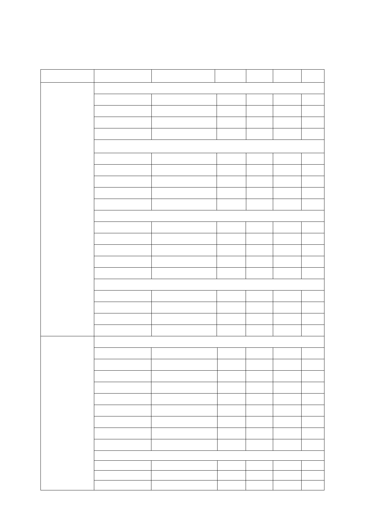
8. Electrical Characteristics
8.1. Absolute Maximum Ratings
Absolute maximum ratings are stress ratings only. Permanent damage to the device may be caused by
continuously operating at or beyond these limits. Device functional operating limits and guaranteed
performance specifications are given under electrical characteristics at the test conditions specified.
Symbol
Parameter
MIN
MAX
Unit
LDO_IN
LDO Input power for Audio CODEC
-0.3
3.63
V
VDD_CORE
Digital power for Audio digital core, it can be generate by inner LDO
-0.3
1.32
V
VCC_IO1
Digital power for digital I/O buffer (I2S1)
-0.3
3.63
V
VCC_IO0
Digital power for digital I/O buffer (I2C and RSB)
-0.3
3.63
V
CPVDD
Analog power for headphone charge pump
-0.3
2.0
V
A
T
Operating Ambient Temperature
-20
85
℃
VESD
ESD
4
--
KV
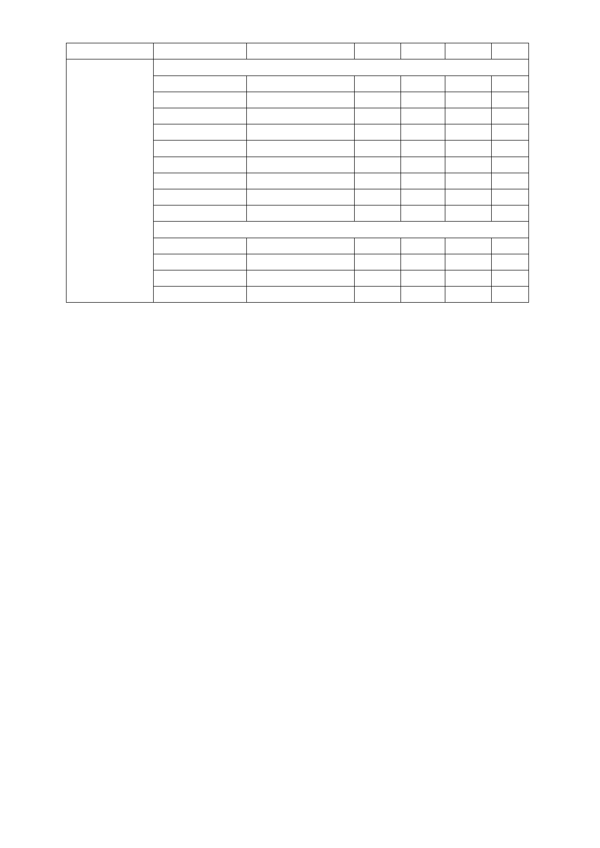
8.2. Recommended Operating Conditions
Parameter
Description
MIN
TPY
MAX
Unit
LDO_IN
LDO Input power for Audio CODEC
1.35
1.8/1.5
3.63
V
VDD_CORE
Digital power for Audio digital core, it can be generate by inner
LDO
1.08
1.2
1.32
V
VCC_IO1
Digital power for digital I/O buffer (I2S1)
--
1.8/3.3
3.63
V
VCC_IO0
Digital power for digital I/O buffer (I2C and RSB)
--
1.8/3.3
3.63
V
CPVDD
Analog power for headphone charge pump
1.2
1.8
1.98
V
GND,AGND
Ground reference
--
0
--
V
8.3. Static Characteristics
Symbol
Parameter
Test condition
Min
Typical
Max
Units
IN
V
Input Voltage Range
--
-0.3
--
VCCIO1+0.3
VCCIO2+0.3
V
IH
V
High Level Input Voltage
VCCIO=3.0v
2.4
--
3.6
V
VCCIO=1.8V
1.4
--
1.98
IL
V
Low Level Input Voltage
VCCIO=3.0v
-0.3
--
0.7
V
VCCIO=1.8V
-0.3
--
0.7
OH
V
High Level Input Voltage
VCCIO=3.0v
2.7
--
NA
V
VCCIO=1.8V
1.5
--
NA
OL
V
Low Level Input Voltage
VCCIO=3.0v
NA
--
0.4
V
VCCIO=1.8V
NA
--
0.4
OZ
I
Tri-state Output Leakage Current
--
TBD
TBD
TBD
uA
IN
C
Input Capacitance
--
NA
NA
5
pF
OUT
C
Output Capacitance
--
NA
NA
5
pF
9. Analog Performance Characteristics
PARAMETER
TEST CONDITIONS
MIN
TYP
MAX
UINT
DAC Output Path
Performance
DAC to Headphone on HPOUTL or HPOUTR(R=10kΩ)
FScale Output Level
0dB 1KHz
0.9
Vrms
SNR(A-weighted)
0dB 1KHz
100
dB
THD+N(NO-Aweight)
0dB 1KHz
-84
dB
Crosstalk(L/R)
0dB 1KHz
-88/-88
dB
DAC to Headphone on HPOUTL or HPOUTR(R=16Ω)
FScale Output Level
0dB 1KHz
0.5
Vrms
SNR(A-weighted)
0dB 1KHz
99
dB
THD+N(P0=15mW)
0dB 1KHz
-81
dB
THD+N(P0=5mW)
0dB 1KHz
-82
dB
Crosstalk(L/R)
0dB 1KHz
-82/-82
dB
DAC to Headphone on HPOUTL or HPOUTR(R=32Ω)
FScale Output Level
0dB 1KHz
0.7
Vrms
SNR(A-weighted)
0dB 1KHz
100
dB
THD+N(P0=15mW)
0dB 1KHz
-83
dB
THD+N(P0=5mW)
0dB 1KHz
-83
dB
Crosstalk(L/R)
0dB 1KHz
-86/-86
dB
DAC to SPK signal on SPKOUTLP and SPKOUTLN(R=10KΩ)
FScale Output Level
0dB 1KHz
1.8
Vrms
SNR(A-weighted)
0dB 1KHz
102
dB
THD+N
0dB 1KHz
-82
dB
DC Offset at load
0dB 1KHz
0.7
mV
ADC Input Path
Performance
MIC1 /2 to ADC via ADC mixer
FScale Input Level
0dB Gain 1KHz
0.5
Vrms
SNR(A-weighted)
-1dB 1KHz, 0dB Gain
96
dB
THD+N
-1dB 1KHz, 0dB Gain
-85
dB
SNR(A-weighted)
30mV,1KHz, 30dB Gain
81
dB
THD+N
30mV,1KHz, 30dB Gain
-76
dB
SNR(A-weighted)
30mV,1KHz, 39dB Gain
81
dB
THD+N
30mV,1KHz, 39dB Gain
-76
dB
SNR(A-weighted)
10mV,1KHz, 48dB Gain
73
dB
THD+N
10mV,1KHz, 48dB Gain
-72
dB
LINEIN to ADC via ADC mixer
FScale Input Level
0dB 1KHz
0.9
Vrms
SNR(A-weighted)
1KHz
93
dB
THD+N
1KHz
-85
dB
Crosstalk(L/R)
1KHz
-85/-85
dB
Bypass Path
Performance
MIC1/2 to Headphone via output mixer
FScale Input Level
0dB Gain 1KHz
0.5
Vrms
SNR(A-weighted)
-1dB 1KHz, 0dB Gain
98
dB
THD+N
-1dB 1KHz, 0dB Gain
-91
dB
SNR(A-weighted)
30mV,1KHz, 30dB Gain
83
dB
THD+N
30mV,1KHz, 30dB Gain
-78
dB
SNR(A-weighted)
30mV,1KHz, 39dB Gain
83
dB
THD+N
30mV,1KHz, 39dB Gain
-79
dB
SNR(A-weighted)
10mV,1KHz, 48dB Gain
74
dB
THD+N
10mV,1KHz, 48dB Gain
-73
dB
LINEIN to Headphone via output mixer
FScale Input Level
0dB 1KHz
1
Vrms
SNR(A-weighted)
-1dB 1KHz
98
dB
THD+N(-1dBFS)
-1dB 1KHz
-92
dB
Crosstalk(L/R)
-1dB 1KHz
-89/-89
dB

10. Typical Power Consumption
Default Test Conditions:
LDOIN=CPVDD=1.5V,AVCC=3.0V,VCC-IO1=1.8V,VCC-IO0=3.0V
OPERATING
MODE
TEST CONDITIONS
LDOIN
AVCC
VCC-IO1
VCC-IO0
CPVDD
LDO enabled
XTAL enabled
LDOIN,VCC-IO0 supplies,
32.768KHz clock,
1.8V
3V
1.8V
3V
1.8V
0uA
0uA
0uA
12uA
0uA
LDO enabled
XTAL enabled
All supplies present,
No clocks supply,
Default register settings
1.8V
3V
1.8V
3V
1.8V
73uA
62uA
0uA
12uA
0uA
AIF1 to DAC to
HPOUT(stereo)
fs=44.1KHz,
SYSCLK=MCLK=24.576MHz,
24bit I2S,Slave mode
1.8V
3V
1.8V
3V
1.8V
1.5mA
4.1mA
0.013mA
12uA
2.4mA
MIC1 to ADC to
AIF1(mono)
fs=44.1KHz,
SYSCLK=MCLK=24.576MHz,
24bit I2S,Slave mode
1.8V
3V
1.8V
3V
1.8V
1.4mA
4.5mA
0.023mA
12uA
0mA
Mic1 to Lineout,
Linein to Hp,
fs=8 kHz,
SYSCLK=MCLK=24.576MHz
1.8V
3V
1.8V
3V
1.8V
0.75mA
4.1mA
0mA
12uA
2.0mA
11.Function Description
11.1. Power
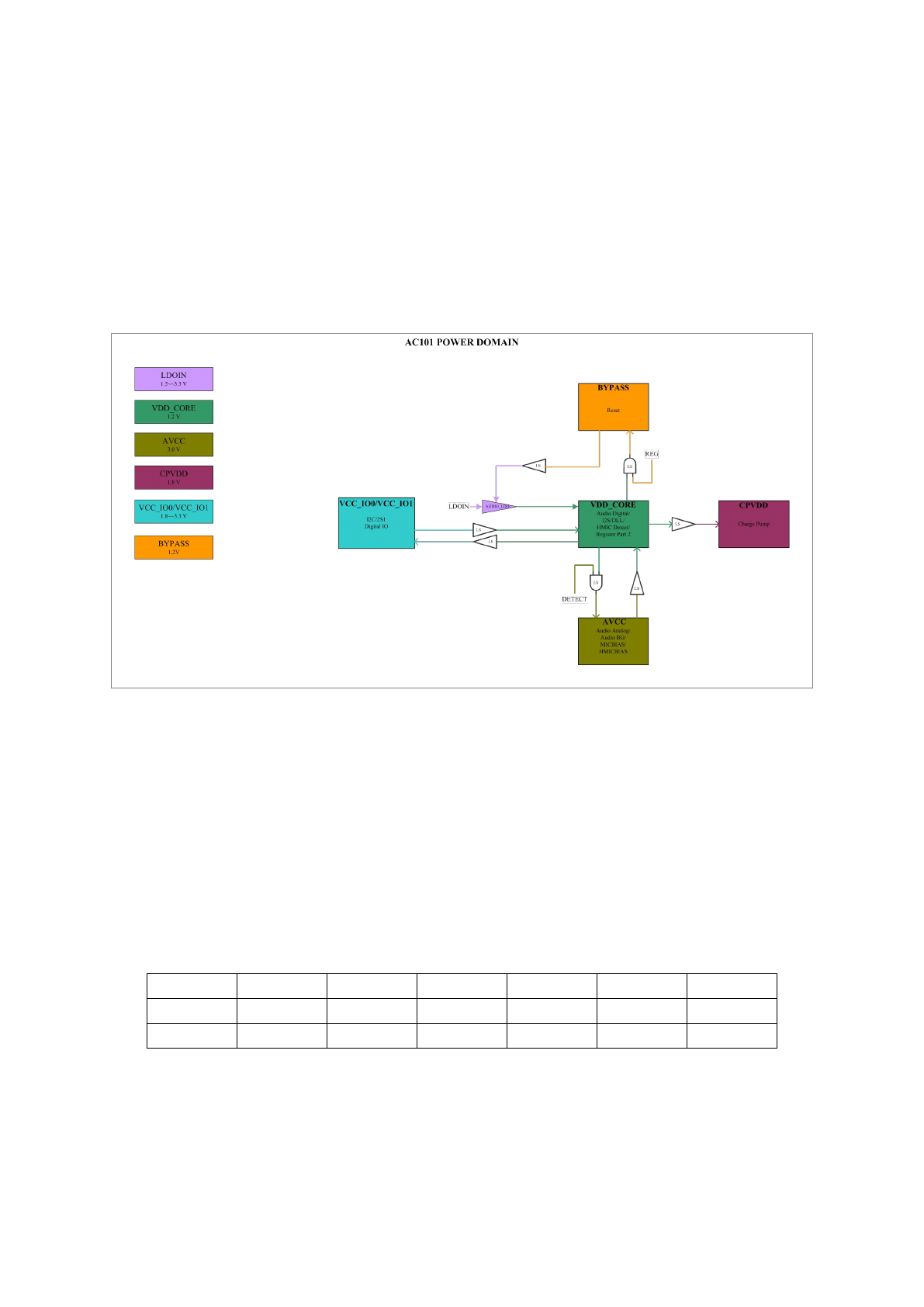
There are a Power-Reset circuit in AC101 used to reset all the circuit and register to a standby state after
power up. The Power-Reset circuit make all the supply power need no specific timing. All the supply
voltages are illustrated in the below figure.
Figure 5 Power Management
VDD-CORE is 1.2V for audio digital core power generated from LODIN pin, which also can be direct
supplied from VDD-CORE pin. VDD-IO0 is digital I/O power for I2C/RSB . VDD-IO1 is digital I/O
power for I2S1. AVCC is for analog power. CPVDD for charge pump power.
When the AC101 is not working, it need to set the supply properly to prevent power leakage. There are two
settings to select. It's best to power off all the supply. The other is to make sure AVCC and CPVDD both
power on.
At the setting below, AC101 has the best performance.
LDOIN
VDD_CORE
AVCC
CPVDD
VCC-IO0
VCC-IO1
BYPASS
1.5~~3.3 V
1.2 V
3 V
1.8 V
1.8/3.3 V
1.8/3.3 V
1.2 V
Supplied
N/A
Supplied
Supplied
Supplied
Supplied
N/A
* VDD_CORE and BYPASS generated by internal LDO.
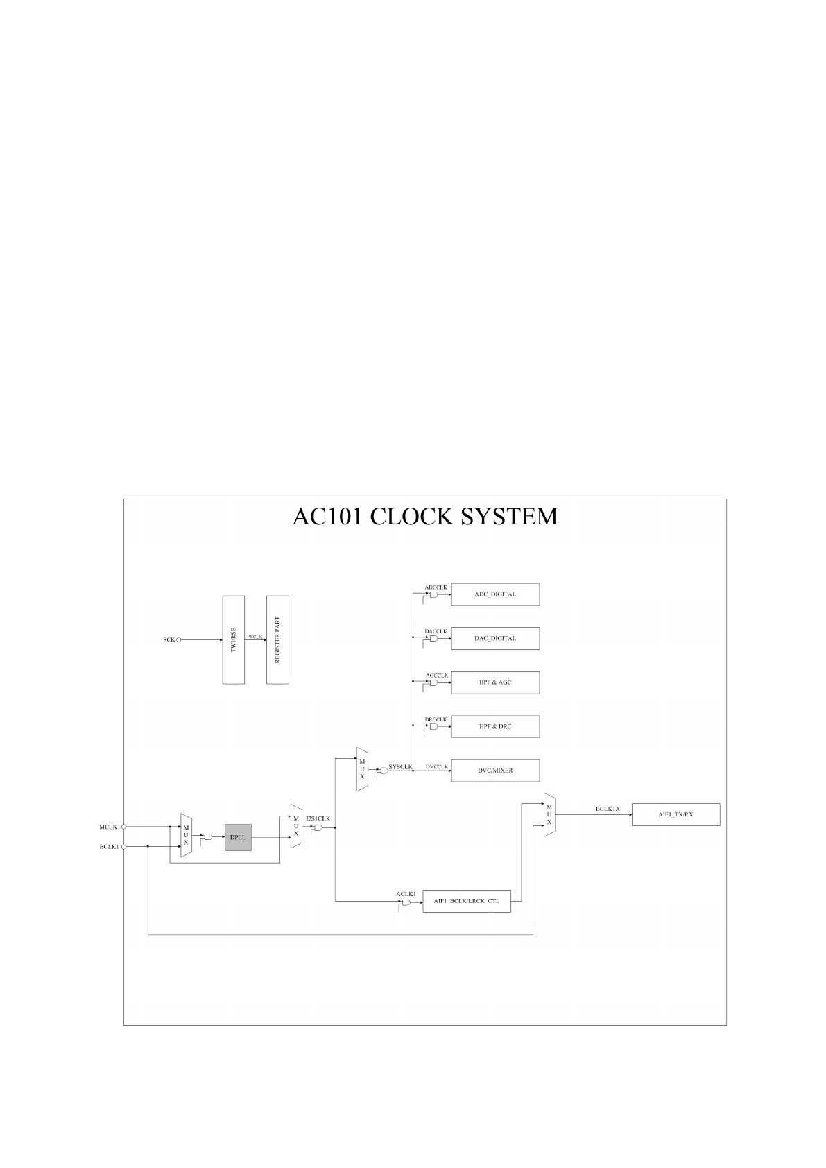
11.2. Clock
The system clock(SYSCLK) of AC101 must be 512*fs(fs=48KHz or 44.1KHz). So the system should
arrange the divider to generate 24.576MHz for audio clock series of 48KHz or 22.5792MHz for series of
44.1KHz.
SYSCLK is the reference of ADC, DAC, DVC, MIXER, AGC and DRC module. SYSCLK can be selected
from I2S1CLK which derived from MCLK1 or PLL. MCLK1 are always provided externally while the
PLL reference clock can be select from MCLK1 and BCLK1.
I2S1CLK is the reference of the first I2S clocking zone. In master mode, LRCK and BCLK are derived
internally from I2SnCLK. In slave mode, LRCK and SCLK are supplied externally and BCLK can be used
as the PLL input reference.
There are also an internal Oscillator to generate a clock signal for direct-path mode. In this mode, the
oscillator supply clock to charge pump, adjustment circuit, headphone detect circuite.g... In direct-path case,
no external clock need .
Figure 6 Clocking Management
11.3. PLL
A Phase-Locked Loop(PLL) is used to provide a flexible input clock range from 128KHz to 24MHz. The
source of the PLL can be set to MCLK1 or BCLK1 by setting register. The PLL output is always used to
provide the system clock(SYSCLK) of AUDIO codec when 24.576MHz or 22.5792MHz can not be
provided from MCLK.
The PLL transmit formula as below:
FOUT =(FIN * N) / (M * (2K+1)) ; (N= N_i + 0.2*N_f)
Table 1 clock setting for SYSCLK=24.576 MHz
FIN
M
N
K
FOUT
128K
1
576
1
24.576M
192K
1
384
1
24.576M
256K
1
288
1
24.576M
384K
1
192
1
24.576M
...
....
...
1
24.576M
6M
25
307.2
1
24.576M
13M
42
238.2
1
24.576M
19.2M
25
96
1
24.576M
Table 2 clock setting for SYSCLK=22.5792 MHz
FIN
M
N
K
FOUT
128K
1
529.2
1
22.5792M
192K
1
352.8
1
22.5792M
256K
1
264.6
1
22.5792M
384K
1
176.4
1
22.5792M
...
....
...
1
22.5792M
6M
38
429
1
22.5789M
13M
19
99
1
22.5789M
19.2M
25
88.2
1
22.5792M
11.4. TWI/RSB Interface
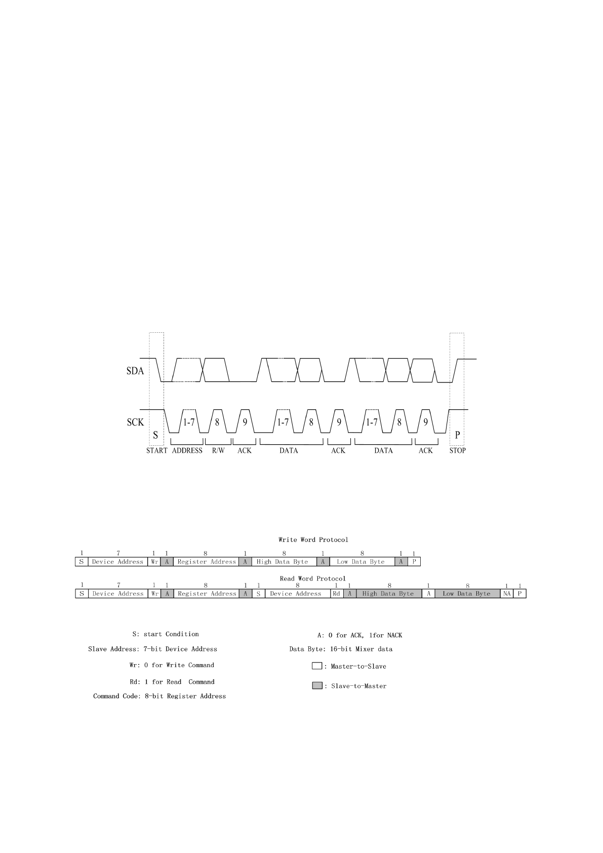
AC101 can support two series control interface protocol for writing to or read back from registers on SCK
and SDA pins . One is TWI interface, the other is RSB interface. RSB is top-priority for higher efficiency
and lower power consumption.
11.4.1. TWI Interface
TWI is a 2-wire (SCK/SDA) half-duplex serial communication interface, supporting only slave mode. SCK
is used for clock and SDA is for data. SCK clock supports up to 400 KHz rate and SDA data is a open drain
structure.
A master controller initiates the transmission by sending a “start” signal, which is defined as a high-to-low
transition at SDA while SCK is high. The first byte transferred is the slave address. It is a 7-bit chip address
followed by a R/W bit. The chip address must be 0011010x. The R/W bit indicates the slave data transfer
direction. Once an acknowledge bit is received, the data transfer starts to proceed on a byte-by-byte basis in
the direction specified by the R/W bit. The master can terminate the communication by generating a “stop”
signal, which is defined as a low-to-high transition at SDA while SCK is high.
Figure 7 TWI Interface
The formats of “write” and “read” instructions are shown in below.
Figure 8 TWI Read and Write
11.4.2. RSB Interface
RSB interface supports a special protocols with a simplified two wire protocol on a push-pull bus. So the
transfer speed can be up to 10MHz and the performance will be improved much. AC101 works only in
slave mode.
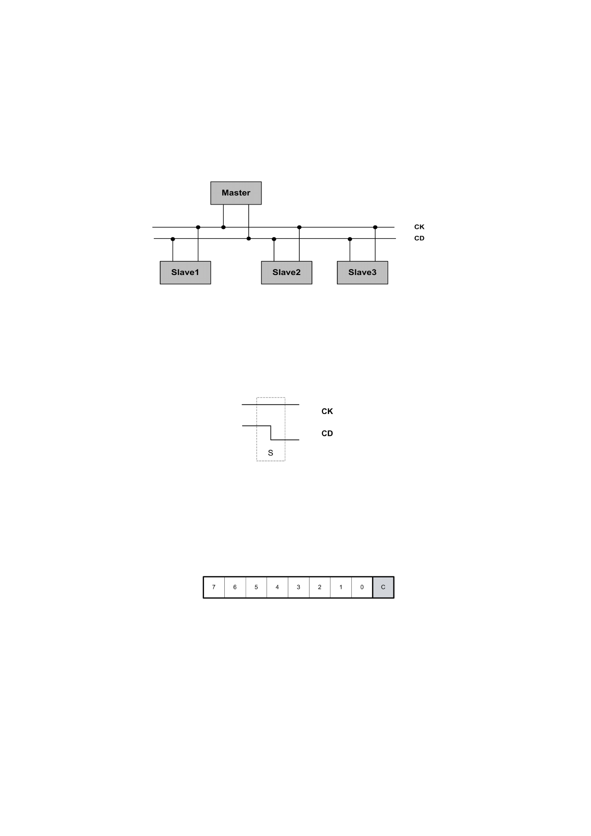
RSB support multi-slaves. It uses CK as clock and uses CD to transmit command and data.the Bus
Topology is showed below:
Figure 9 RSB Bus Topology
The start bit marks the beginning of a transaction with the slave device.When CK is high, a change from
high to low on CD is defined as a start condition. This start condition notifies the selected device to start a
transfer.
Figure 10 Start signal
RSB protocol uses parity bit to check the correction of every byte,The checked object is the 7, 8 or 15 bit in
front of the parity bit.
Figure 11 Parity bit
ACK bit is the acknowledgement from device to host, The ACK is active low. When device finds the parity
bit is error, it will not send ACK to host, so host can know that an error happens in the transaction.
Set run-time slave address(RTSADDR) command. It is used to set run time slave address(RTSADDR) for
different devices in the same system. There are 15 devices in a system at most. The RTSADDR can be
selected from the command code set and a device 's RTSADDR can be modified many times by using set
run-time slave address command.
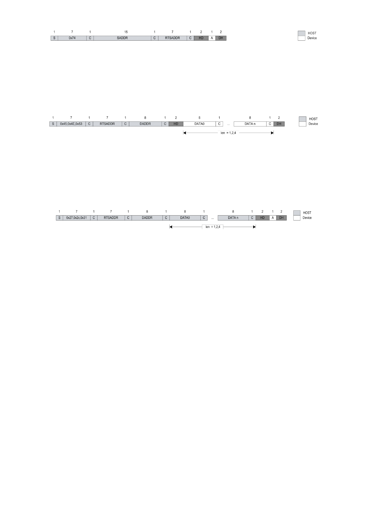
Figure 12 RTSADDR command
Read command is used to read data from device.It has byte,half word and word operation.When devices
receives the command,they shall check if the command's RTSADDR matches their own RTSADDR.The
device's RTSADDR is set by set run-time slave address(RTSADDR) command.
Figure 13 Read command
Write command is used to write data to the devices.It has byte,half word and word operation.When devices
receive the command,they shall check if the command's RTSADDR matches their own RTSADDR.The
device's RTSADDR is set by set run-time slave address(RTSADDR) command.
Figure 14 Write command
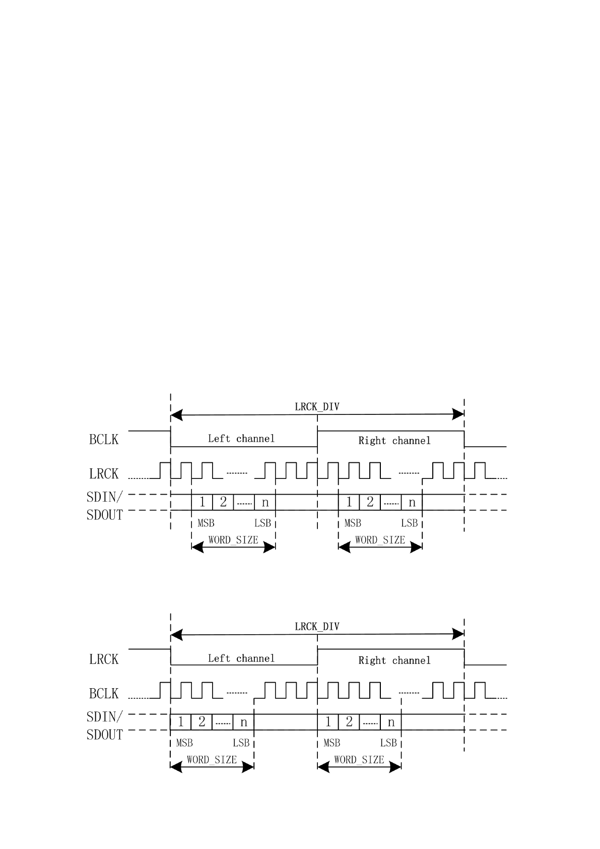
11.5. I2S/PCM Interface
There are one I2S/PCM interface which can be configured as master mode or slave mode in AC101. In the
general case, the digital audio interface uses four pins as below:
-BCLK: Bit clock for data synchronization
-LRCK: Left/Right data alignment clock
-SDOUT: output data for ADC data
-SDIN: input data for DAC data
I2S audio interface support four different data formats as below. On the I2S interface, TDM is available for
all four formats and AC101 can use it to transmit or receive up to four channel data on timeslot0 and
timeslot1 simultaneously.
-I2S mode
-Left justified mode
-Right justified mode
-PCM short mode
Figure 15 I2S Justified mode
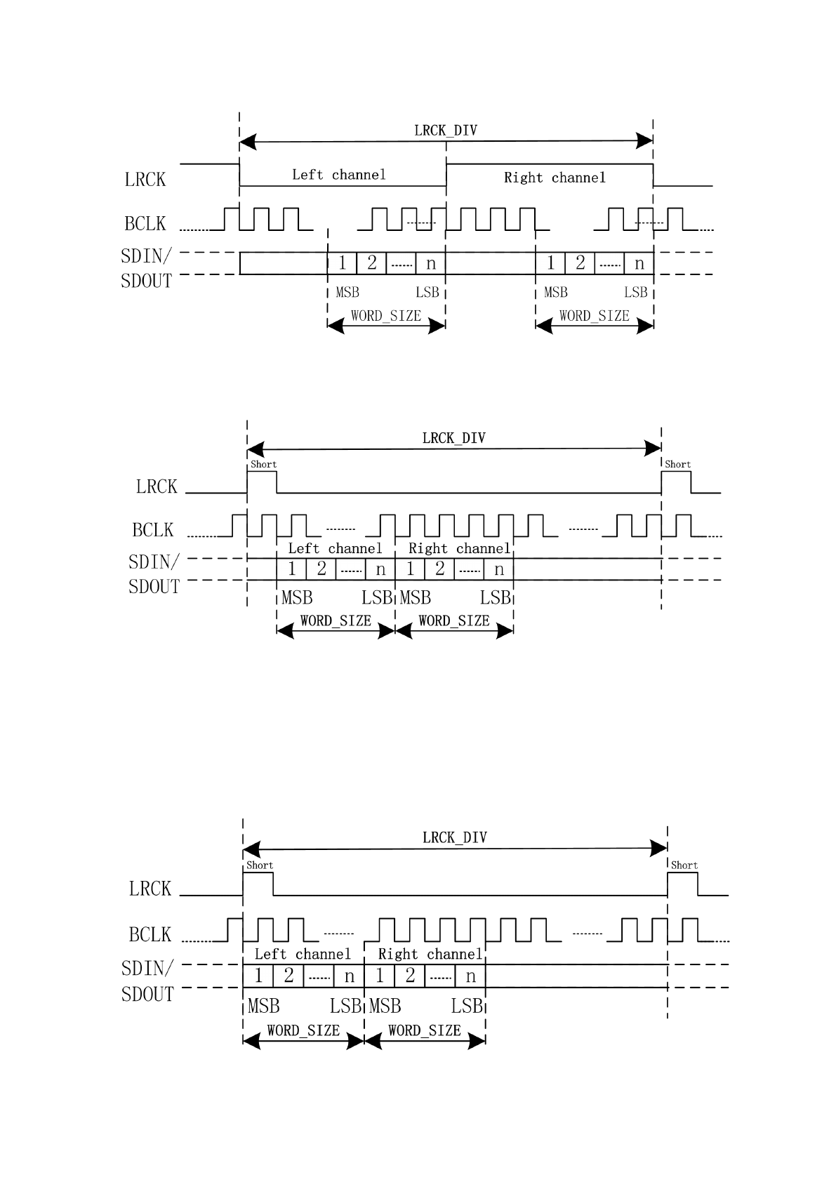
Figure 16 Left Justified mode
Figure 17 Right Justified mode
Figure 18 Pcm mode A(LRCK_INV=0)
Figure 19 Pcm mode B(LRCK_INV=1)
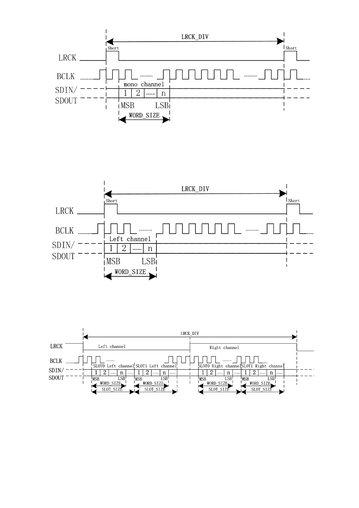
Figure 20 Pcm mode A mono(LRCK_INV=0)
Figure 21 Pcm mode B mono(LRCK_INV=1)
Figure 22 I2S TDM mode
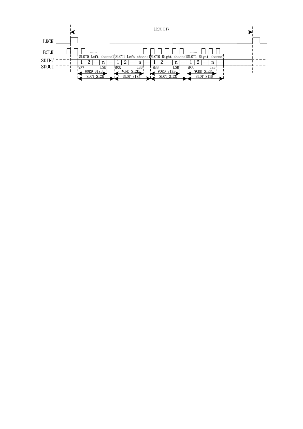
Figure 23 PCM TDM mode

11.6. Stereo ADC
The stereo ADC is used for recording stereo sound. The sample rate of the stereo ADC can not be
independent of DAC sample rate. In other words, the stereo ADC and DAC must work at a same sample
rate. The sample rate is configured by the register ADDA_FS_I2S1.
In order to save power, the left and right analog ADC part can be enabled/disabled separately by setting
register ADC_APC_CTRL Bit15 & Bit11. The digital ADC part can be enabled/disabled by
ADC_DIG_CTRL Bit15.
The volume control of the stereo ADC is set via register ADC_APC_CTRL Bit14:12 & ADC_APC_CTRL
Bit10:8.
11.7. Stereo DAC
The stereo DAC sample rate is the same as the stereo ADC. The sample rate is configured by the register
ADDA_FS_I2S1.
In order to save power, the left and right DAC can be enabled/disabled separately by setting register
OMIXER_DACA_CTRL Bit15:14. The digital DAC part can be enabled/ disabled by DAC_DIG_CTRL
Bit15.
11.8. Mixer
The Codec supports three series of mixers for all function requirements:
-2 channels DAC Output mixers
-2 channels ADC Record mixers
-Digital mixers
11.8.1. DAC Output Mixers
The output mixer is used to drive analogue output, including headphone, earpiece, speaker,lineout. The
following signals can be mixed into the output mixer:
-LINEINL/R
-MIC1P/N,MIC2P/N
-Stereo DAC output
11.8.2. ADC Record Mixers
The ADC record mixer is used to mix analog signals as input to the Stereo ADC for recording. The
following signals can be mixed into the output mixer:
-LINEINL/R
-MIC1P/N,MIC2P/N
-Stereo DAC output
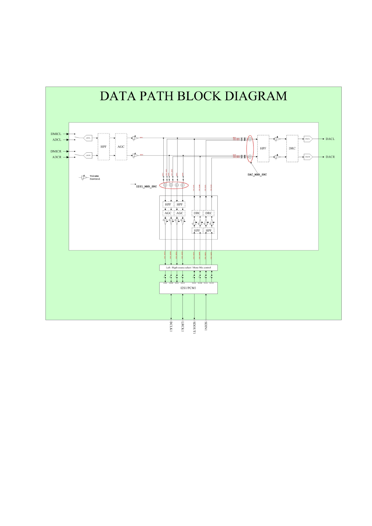
11.8.3. Digital Mixers
The digital mixers are provided for digital audio data mixing on one I2S path, two ADC output paths and
two input paths to the stereo DAC. It's separately controlled by the register I2S1_MXR_SRC and
DAC_MXR_SRC.
Figure 24 Digital Data Path
11.9. Analogue Audio Input Path
The codec supports five Analogue Audio Input paths:
-LINEINL/R
-MIC1P/N,MIC2P/N
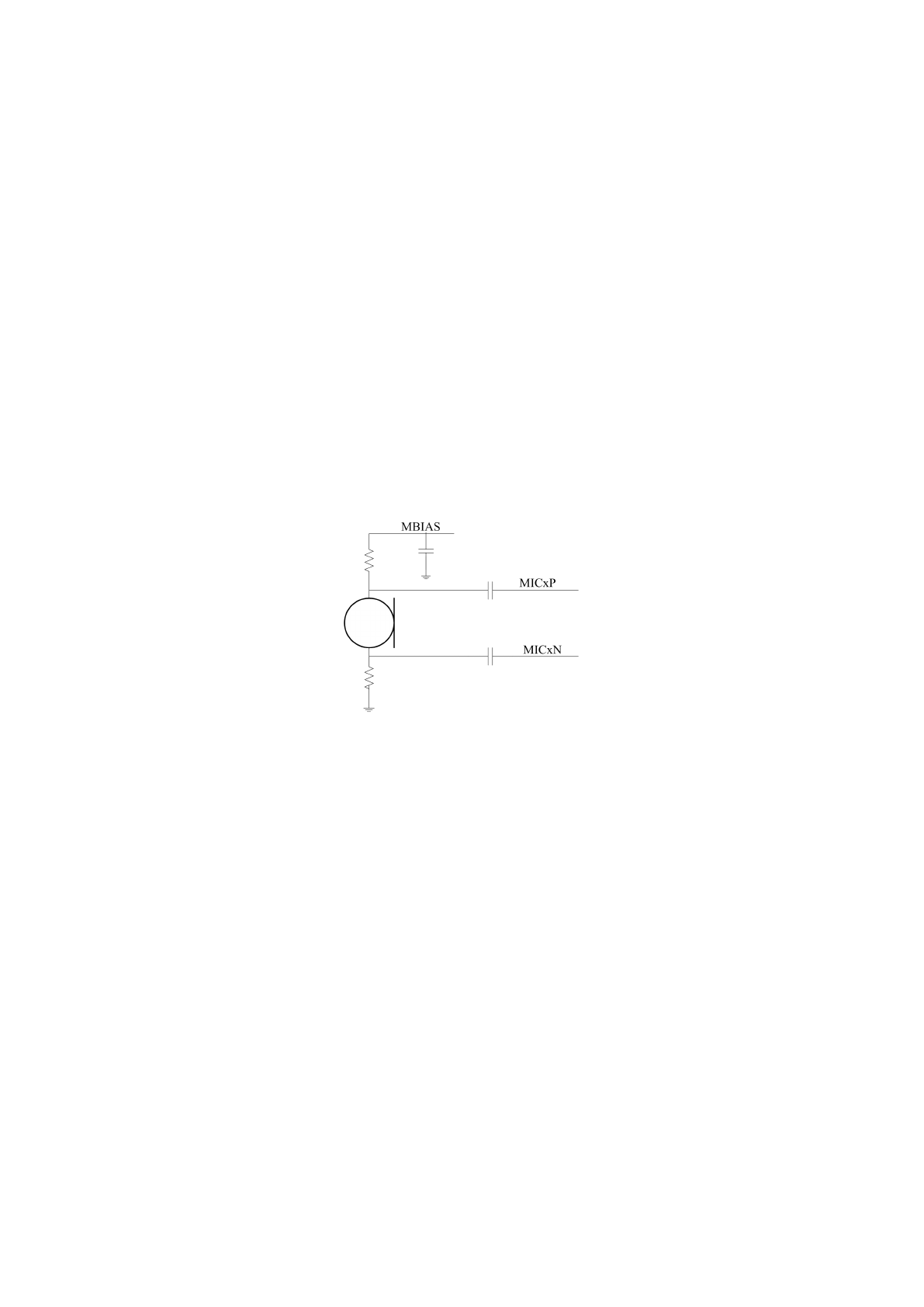
11.9.1. Microphone Input
MICIN1P/N, MICIN2P/N provide differential input that can be mixed into the ADC record mixer, or DAC
output mixer. MICIN is high impedance, low capacitance input suitable for connection to a wide range of
differential microphones of different dynamics and sensitive. There are two microphone pre-amplifiers for
the 2 differential microphone inputs. MICIN1P/N are input to the first pre-amplifier, MICIN2P/N
multiplexed as digital pin DMICCLK/DMICDAT are input to the 2nd pre-amplifier . Each microphone
pre-amplifier has a separate enable bit, ADC_SRCBST_CTRL Bit15 & Bit11. The gain for each
pre-amplifer can be set independently using MIC1BOOST, MIC2BOOST. MBIAS provide reference
voltage for electret condenser type(ECM) microphones.
Figure 25 Suggested External Microphone Input
11.9.2. LINEINL/R Input
LINEINL/R provide one-channel mono differential input or stereo single-ended input that can be mixed
into the ADC record mixer or the stereo output mixer. The inputs are suited to receiving line level signals
such as external audio equipment or baseband module .
When the linein input is set as differential signal input LINEINL-LININR to the ADC or to DAC mixer, the
linein gain is logarithmically adjustable from -9dB to 12dB in 1.5dB step by the register
LINEIN_DIFF_PREG set.
11.10. Analogue Audio Output Path
The codec supports five Analogue Audio Output paths:
-HPOUTL/R, HPOUTFB
-SPOLP/N
-SPORP/N
11.10.1. Headphone Output
HPOUTL/R provides two-channel single-ended output to headphone driver. The HPOUTL/R PA input
source can be selected from output mixer or directly from DAC by register HPOUT_CTRL Bit15 & Bit14
set. It also can be muted by register HPOUT_CTRL Bit13 & Bit12 set. The headphone PA power up or
down by register HPOUT_CTRL Bit11 set.
HPOUTL/R can drive a 16R or 32R headphone load without DC capacitors by using Charge Pump to
generate the negative rails. HPOUTFB is the ground loop noise rejection feedback. HBIAS provides
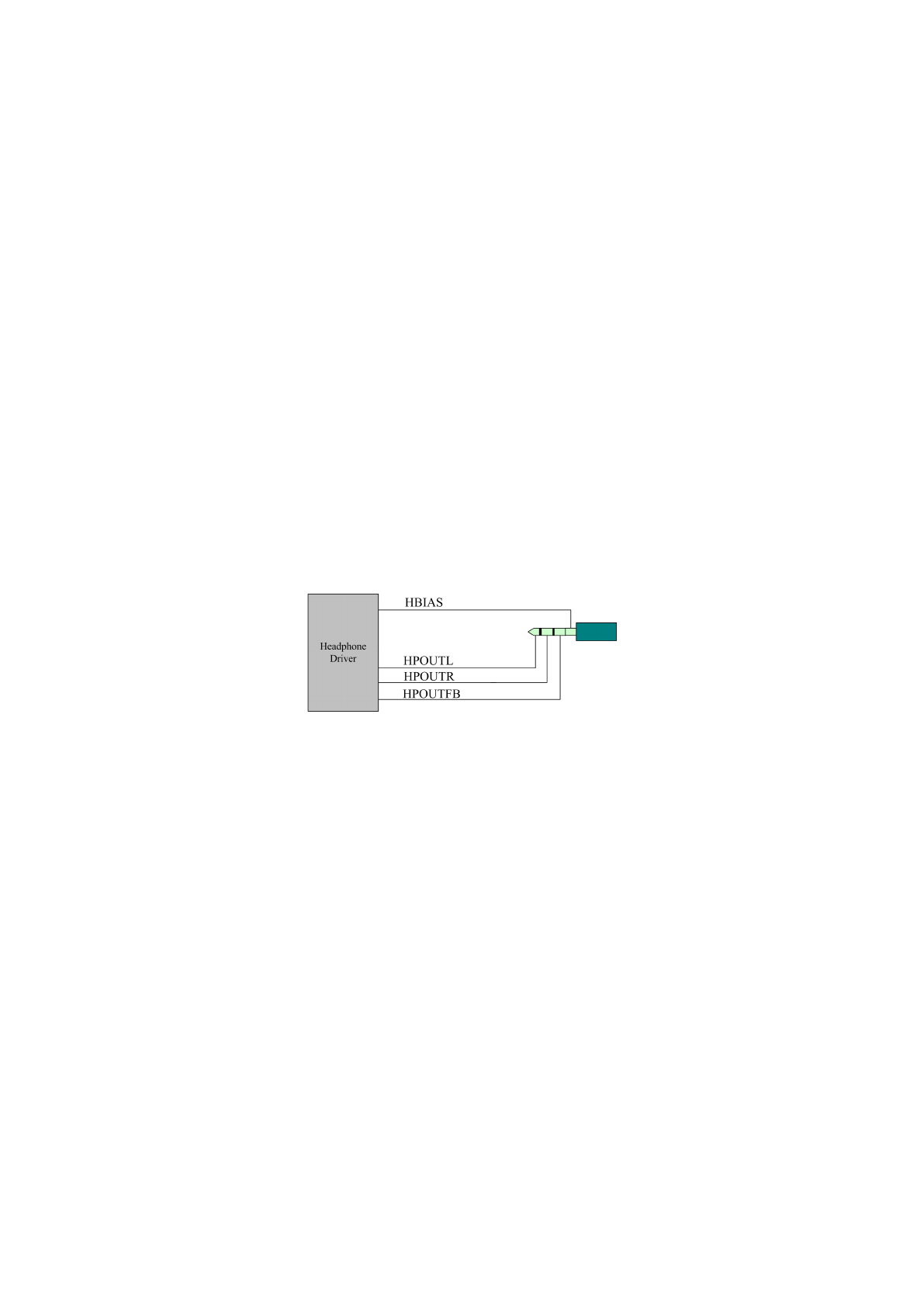
reference voltage for electret condenser type(ECM) microphones. Audio jack insert/ button press detection
function is also provided through measuring the HBIAS current.
Figure 27 Suggested Headphone Output Application
HPOUTL/R volumes can be independently adjusted under software control using the HP_VOL[5:0] of the
headphone output control registers. The adjustment is logarithmic with an 64dB rang in 1dB step from 0dB
to -62dB. The headphone outputs can be muted by writing codes 0x0 to HP_VOL[5:0] bits.
There are a DC offset cancellation circuit to remove the headphone output DC offset for preventing POP
noise in AC101. The function can be enabled or disabled by the register HP_DCRM_EN. This bit must be
set 0xf before headphone PA enabled, and this bit must be set 0x0 before headphone PA disabled.
A zero cross detect circuit is provided at the input to the headphones under the control of the ZCROSS_EN
bit . Using these controls the volume control values are only updated when the input signal to the gain stage
is close to the analogue ground level. This minimizes and audible clicks and zipper noise as the gain values
are changed or the device muted.
11.10.2. Speaker Output
SPOLP/N, SPORP/N provides two differential output without internal speaker amplifier. Using external
amplifier, a stereo speakers can be implemented. The SPOLP/N input source can be selected from left
output mixer or (left+right) output mixer. The SPORP/N input source can be selected from right output
mixer or (left+right) output mixer. So in mono speaker application, The best choice for SPOLP/N or

SPORP/N input source is selected from (left+right) output mixer avoiding sound loss. The volume control
is logarithmic with an 43.5dB rang in 1.5dB step from -43.5dB to 0dB. The left and right speaker output
buffer can independently power up or down by register SPKOUT_CTRL Bit11 & Bit7 set.
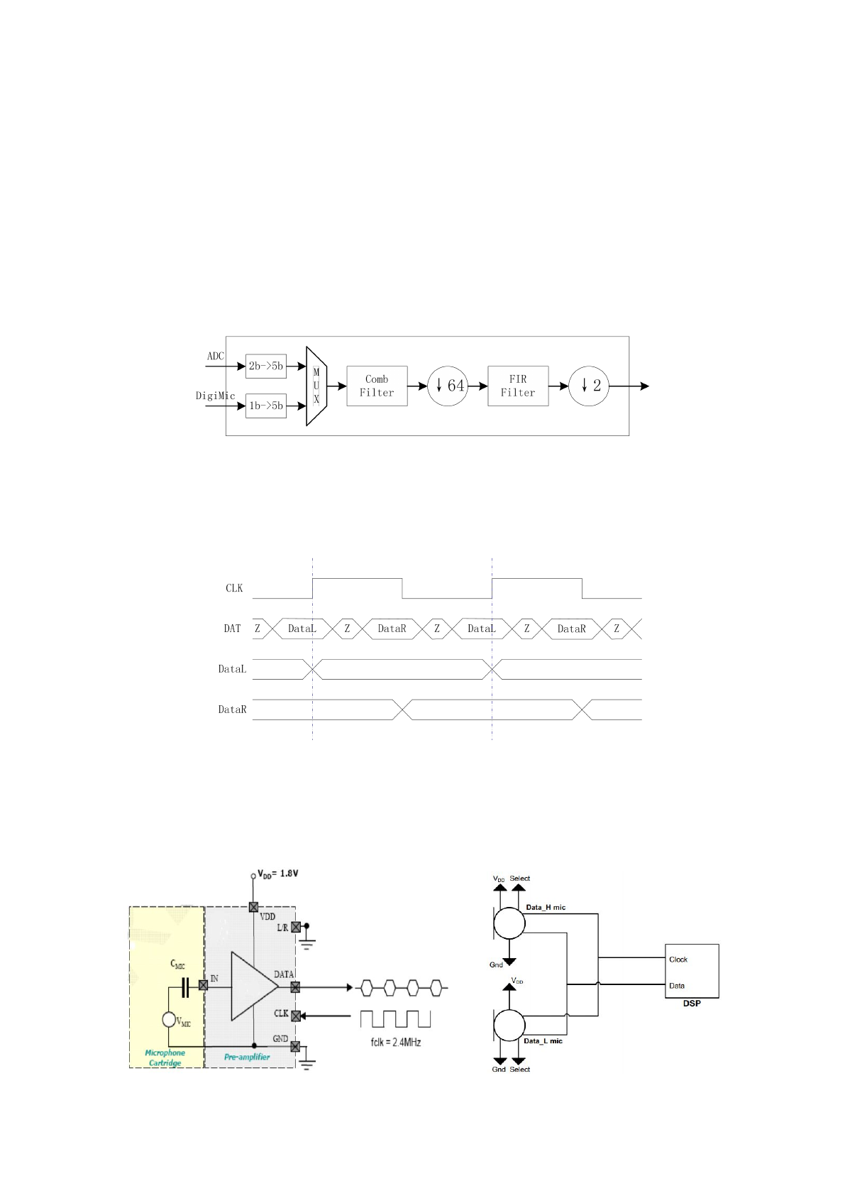
11.11. Digital Microphone Interface
AC101 supports a stereo digital microphone interface. The DMICCLK/ DMICDAT pins are multiplexed on
the MIC3P/MIC3N pins. The circuit share decimation filter with audio ADC. And DMICCLK can be
output 128fs (fs= ADC sample rate).
Digital Microphone power usually falls between the range 1.6V-3.6V, typical 1.8V. And the Clock
frequency is between the the range 1.0MHz-3.25MHz, typical 2.4MHz.
Digital Microphone Block Diagram as below:
Figure 28 Digital Microphone Block Diagram
Digital Microphone timing as below:
Figure 29 Digital Microphone timing
Digital Microphone application as below:
Figure 30 Digital Microphone Application
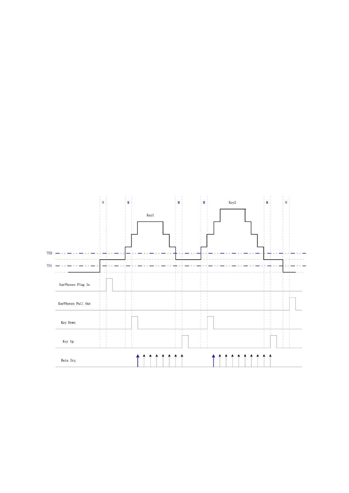
11.12. Audio Jack Detect
The microphone bias output pin HBIAS provide a low noise reference voltage suitable for biasing electrets
type microphones and the associated external resistor biasing network. Hbias is designed to drive headset
microphone, and a bias current detect function is provided for external accessory detection by measuring
the Hbias current. In some application, it's used to detect the insertion/removal of a audio jack and the
button press. These events will cause a significant change in bias current flow, which can be detected and
used to generate a signal to the processor.
When HBIAS current detect is enabled, 5 bit ADC will send out sample data at 16/32/64/128Hz clock rate.
Digital logic trigger an interrupt event controlled by register setting when the data is changed.
The digital circuit generate five IRQ signals that can be disabled by register, the data from ADC can be read
from register HMIC_STATUS Bit12:8.
IRQ Timing Diagram:
Figure 31 HBIAS Detect IRQ Timing Diagram
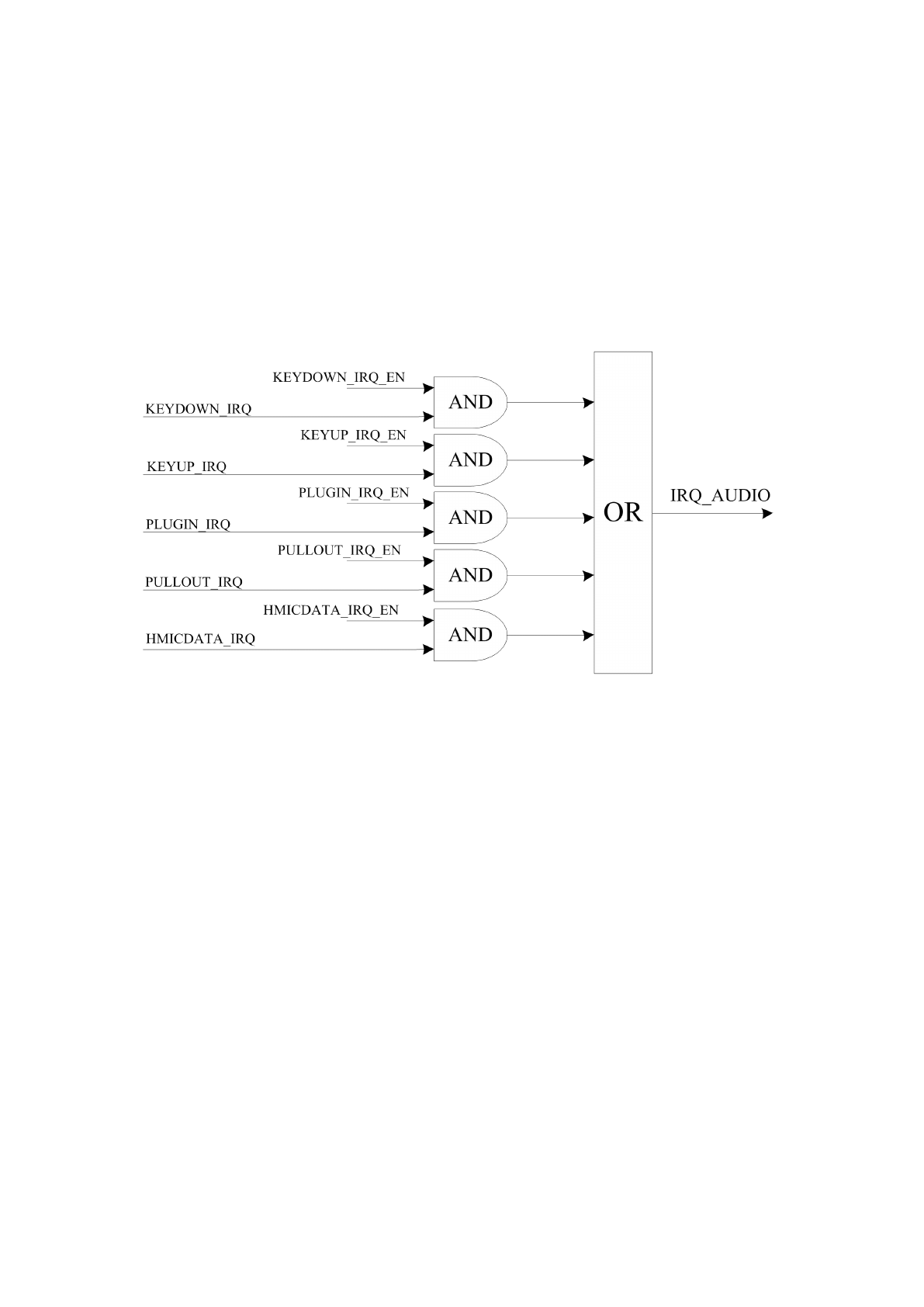
11.13. Interrupt
The Interrupt circuits in AC101 generate an Interrupt (IRQ) event to enable the detection of audio jack
status. The Interrupt pin IRQ_AUDIO is open-drain. It's usually drives a high level voltage via the external
pull-up resistor while it output a low level when the IRQ is active.
It supports the following triggered events illustrated in the figure below:
Figure 32 Interrupt trigger Diagram
11.14. Digital Audio Process for DAC
The DAP System Block Diagram For DAC.
Figure 39 DAC DAP System Block
DAP for DAC Data Flow:
Figure 40 DAC DAP Data Flow
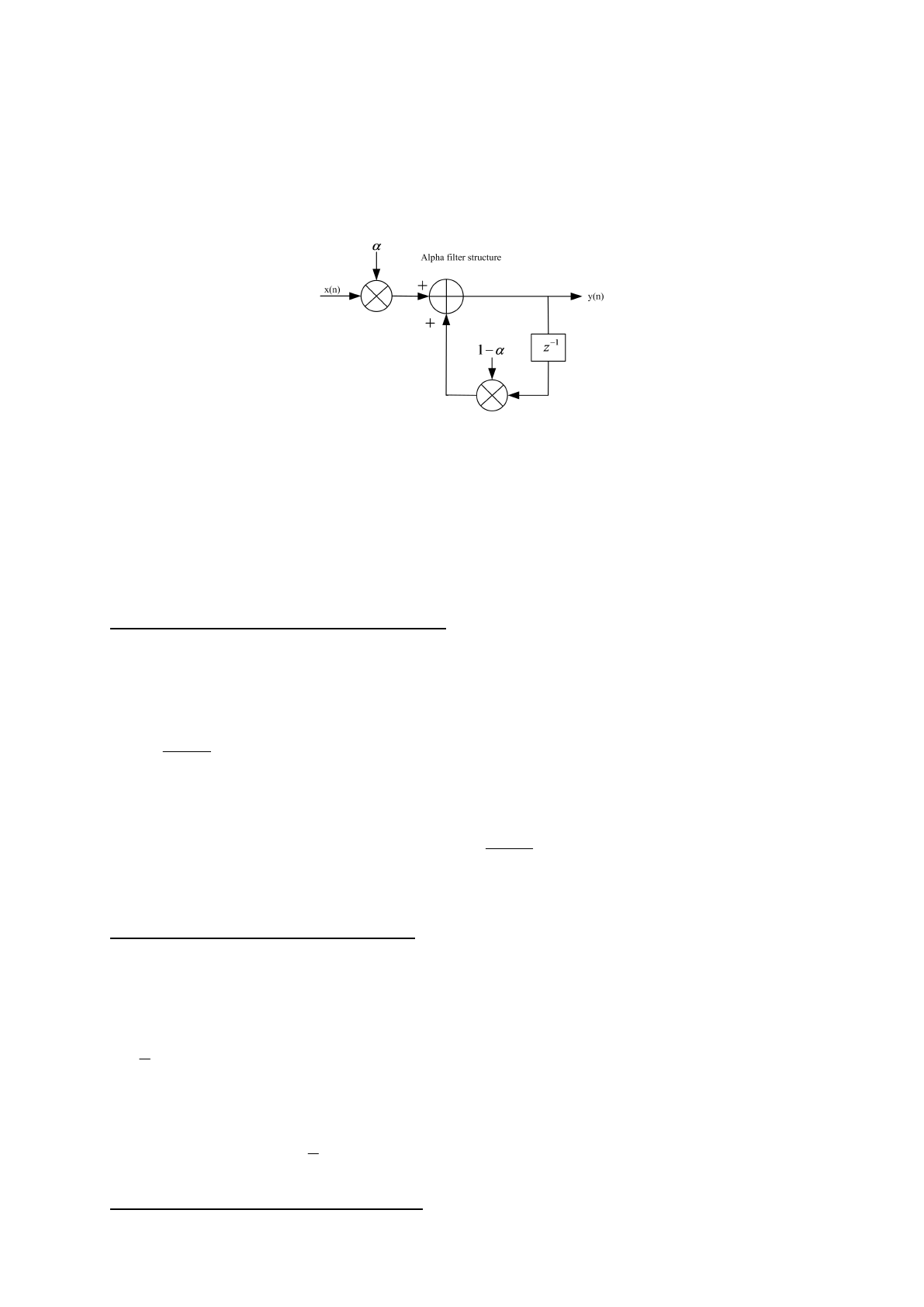
11.14.1. High Pass Filter
The DAP has individual channel high pass filter that can be enabled and disabled. The filter cutoff
frequency is less than 1Hz.
1
1
1
1
)(
az
z
zH
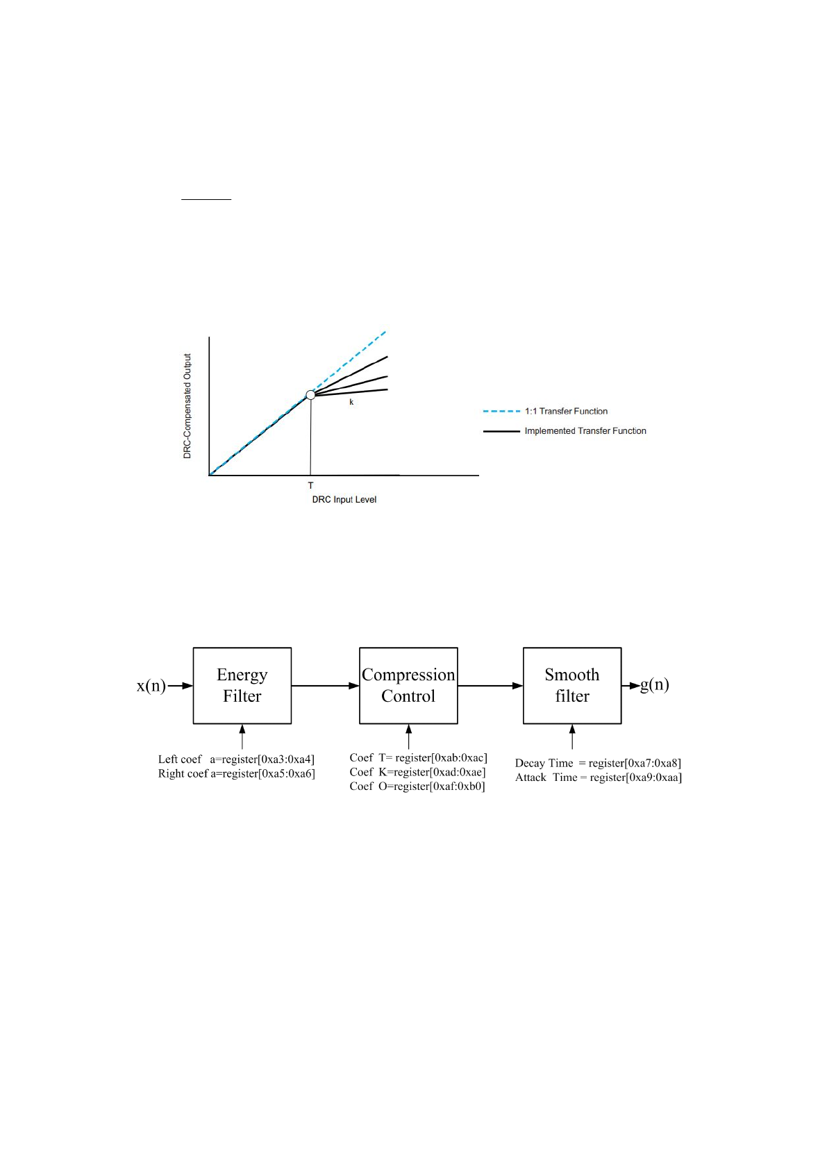
11.14.2. Dynamic Range Control
The dynamic range control(DRC) can be enabled in the digital playback path of AC101. It automatically
adjusts the wide volume gain to flatten volume level.
Figure 41 DRC Response Characteristic
The DRC supports the main feature below:
Figure 42 DRC Block and Register Control
-Adjustable threshold, offset, and compression levels
-Programmable energy coefficient, attack, and decay time constants
-Transparent compression: Compressors can attack fast enough to avoid apparent clipping before
engaging, and decay times can be set slow enough to avoid pumping.
DRC parameter setting
Numbers formatted as N.M numbers means that there are N bits to the left of the decimal point including
the sign bit and M bits to the right of the decimal point. For example, Numbers formatted 3.24 means that
there are 3 bits at the left of the decimal point and 24 bits at the right decimal point.
Energy Filter
The Energy Filter is to estimate of the RMS value of the audio data stream into DRC, and has two
parameters, which determine the time window over which RMS to be made. The parameter is computed by
2.2 /
1Ts ta
e
Figure 43 Energy Filter Structure
Compression Control
This element has three parameters (T, K, O), which are all programmable, and the computation will be
explained as below:
T parameter (Threshold Parameter Computation)
The threshold is the value that determines the signal to be compressed or not. When the signal’s RMS is
larger than the threshold, the signal will be compressed. The value of threshold input to the coefficient
register is computed by
0206.6
dB
T
Tin
There,
dB
T
must less than zero, the positive value is illegal.
For example, it desired to set the T=-30dB, then
982.4
0206.6
30
in
T
, and the 8.24 format of the Tin is
0x04FB_9ED0.
K parameter (Slope Parameter Computation )
The K is the slope within compression region. For example, a n:1 compression means that an output
increase 1dB as RMS input increase n dB. The k input to the coefficient register is computed by
1
1
n
k
There, n is from 1 to 50, and must be integer.
For example, for n=5, the
8.01
5
1k
, and the 3.24 format of the k is 0x733_3333
O parameter (Offset Parameter Computation)
The Ois the offset of the compression static curve. The offset input to the coefficient register is computed
by
20/
10O
in
O
There, Ois -24dB to 24dB.
For example, it desired to set O=6dB, then
6/ 20
10 1.995
in
O
, and the 5.24 format of the
in
O
is
0x1FE_C982.
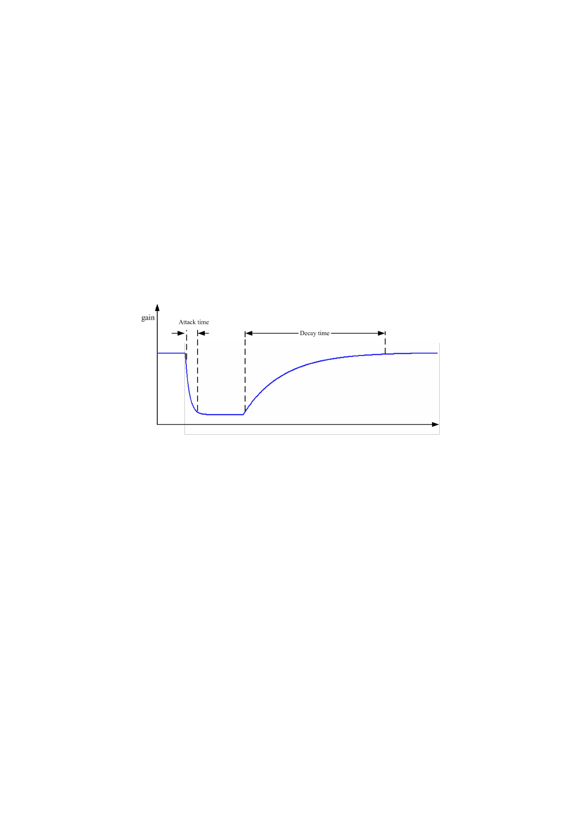
Gain Smooth Filter
The Gain Smooth Filter is to smooth the gain and control the ratio of gain increase and decrease. The decay
time and attack is shown in Figure 5. The structure of the Gain Smooth filter is also the Alpha filter, so the
rise time computation is the same as the Energy filter which is
2.2 /
1Ts ta
e
Figure 44 Smooth Filter Characteristic

12. Register List
Register Name
Offset
Description
CHIP_AUDIO_RST
00H
Chip Soft Reset
PLL_CTRL1
02H
PLL Configure Control 1
PLL_CTRL2
03H
PLL Configure Control 2
SYSCLK_CTRL
04H
System Clocking Control
MOD_RST_CTRL
05H
Module Clock Enable Control
ADDA_SR_CTRL
06H
ADDA Sample Rate Configuration
I2S1LCK_CTRL
10H
I2S1 BCLK/LRCK Control
I2S1_SDIN_CTRL
11H
I2S1 SDIN Control
I2S1_SDOUT_CTRL
12H
I2S1 SDOUT Control
I2S1_DIG_MIXER
13H
I2S1 Digital Mixer Control
I2S1_VOL_CTRL1
14H
I2S1 Volume Control 1
I2S1_VOL_CTRL2
15H
I2S1 Volume Control 2
I2S1_VOL_CTRL3
16H
I2S1 Volume Control 3
I2S1_VOL_CTRL4
17H
I2S1 Volume Control 4
I2S1_MXR_GAIN
18H
I2S1 Digital Mixer Gain Control
ADC_DIG_CTRL
40H
ADC Digital Control
TBD
...
...

Reg 00h_Chip Soft Reset Register
Default: 0x0101
Register Name: CHIP_AUDIO_RST
Bit
Read/Write
Default
Description
15:0
R/W
0x0101
Writing to this register resets all register to their default state.
Reading from this register will indicate device type and version.
Reg 01h_PLL Configure Control 1 Register
Default: 0x0141
Register Name: PLL_CTRL1
Bit
Read/Write
Default
Description
15:14
R/W
0x0
DPLL_DAC_BIAS
00:min
11:max
13:8
R/W
0x1
PLL_POSTDIV_M
PLL Post-Divider Factor M
Factor=0,M=64
Factor=1,M=1
...
Factor=63,M=63
7
R/W
0x0
Reserved
6
R/W
0x1
Close_loop.
1: work as a PLL.
0: work as a free running VCO at a pre-fixed frequency.
5:0
R/W
0x1
INT
Integ[5:0], the loop bandwidth config.
0: works as free running mode.
1: small bandwidth, need more time to lock.
....
63: large bandwidth, need less time to lock, but may result in failing.

Reg 02h_PLL Configure Control 2 Register
Default: 0x0000
Register Name: PLL_CTRL2
Bit
Read/Write
Default
Description
15
R/W
0x0
PLL_EN
PLL Enable
0: Disable
1: Enable
The PLL output FOUT= FIN*N/(M*(2K+1)), N=N_i+N_f;
14
R
0x0
PLL Locked status
0: Not locked or not enabled
1: Enabled and locked
13:4
R/W
0x0
PLL_PREDIV_NI
PLL Integer Part of Pre-Divider Factor N.
Factor=0,N_i=0 ;
Factor=1,N_i=1 ;
...
Factor=1023, N_i=1023 ;
3
/
/
/
2:0
R/W
0x0
PLL_POSTDIV_NF
PLL Fractional Part of Pre-Divider Factor N.
Factor=0,N_f=0*0.2 ;
Factor=1,N_f=1*0.2 ;
...
Factor=7, N_f=7*0.2 ;
Reg 03h_System Clocking Control Register
Default: 0x0000
Register Name: SYSCLK_CTRL
Bit
Read/Write
Default
Description
15
R/W
0x0
PLLCLK_ENA
PLLCLK Enable
0: Disable
1: Enable
14
R/W
0x0
Reserved
13:12
R/W
0x0
PLLCLK_SRC
PLL Clock Source Select
00: MCLK1
01: Reserved
10: BCLK1
11: Reserved
11
R/W
0x0
I2S1CLK_ENA
I2S1CLK Enable
0: Disable
1: Enable
10
R/W
0x0
Reserved

9:8
R/W
0x0
I2S1CLK_SRC
I2S1CLK Source Select
00: MLCK1
01: Reserved
1X: PLL
7:4
R/W
0x0
Reserved
3
R/W
0x0
SYSCLK_ENA
SYSCLK Enable
0: Disable
1: Enable
2:0
R/W
0x0
Reserved
Reg 04h_Module Clock Enable Control Register
Default: 0x0000
Register Name: MOD_CLK_ENA
Bit
Read/Write
Default
Description
15:0
R/W
0x0
Module clock enable control
0-Clock disable
1-Clock enable
BIT15-I2S1
BIT14-Reserved
BIT13-Reserved
BIT12-Reserved
BIT11-Reserved
BIT10-Reserved
BIT9-Reserved
BIT8-Reserved
BIT7-HPF & AGC
BIT6-HPF & DRC
BIT5-Reserved
BIT4-Reserved
BIT3-ADC Digital
BIT2-DAC Digital
BIT1-Reserved
BIT0-Reserved
Reg 05h_Module Reset Control Register
Default: 0x0000
Register Name: MOD_RST_CTRL
Bit
Read/Write
Default
Description
15:0
R/W
0x0
Module reset control
0-Reset asserted
1-Reset de-asserted
BIT15-I2S1
BIT14-Reserved
BIT13-Reserved
BIT12-Reserved
BIT11-Reserved

BIT10-Reserved
BIT9-Reserved
BIT8-Reserved
BIT7-HPF & AGC
BIT6-HPF & DRC
BIT5-Reserved
BIT4-Reserved
BIT3-ADC Digital
BIT2-DAC Digital
BIT1-Reserved
BIT0-Reserved
Reg 06h_ADDA Sample Rate Configuration Register
Default: 0x0000
Register Name: I2S_SR_CTRL
Bit
Read/Write
Default
Description
15:12
R/W
0x0
ADDA_FS_I2S1
ADDA Sample Rate synchronised with I2S1 clock zone
0000: 8KHz
0001: 11.025KHz
0010: 12KHz
0011: 16KHz
0100: 22.05KHz
0101: 24KHz
0110: 32KHz
0111: 44.1KHz
1000: 48KHz
1001: 96KHz
1010: 192KHz
Other: Reserved
11:0
R/W
0x0
Reserved
Reg 10h_I2S1 BCLK/LRCK Control Register
Default: 0x0000
Register Name: I2S1LCK_CTRL
Bit
Read/Write
Default
Description
15
R/W
0x0
I2S1_MSTR_MOD
I2S1 Audio Interface mode select
0 = Master mode
1 = Slave mode
14
R/W
0x0
I2S1_BCLK_INV
I2S1 BCLK Polarity
0: Normal
1: Inverted
13
R/W
0x0
I2S1_LRCK_INV
I2S1 LRCK Polarity
0: Normal
1: Inverted

12:9
R/W
0x0
I2S1_BCLK_DIV
Select the I2S1CLK/BCLK1 ratio
0000: I2S1CLK/1
0001: I2S1CLK/2
0010: I2S1CLK/4
0011: I2S1CLK/6
0100: I2S1CLK/8
0101: I2S1CLK/12
0110: I2S1CLK/16
0111: I2S1CLK/24
1000: I2S1CLK/32
1001: I2S1CLK/48
1010: I2S1CLK/64
1011: I2S1CLK/96
1100: I2S1CLK/128
1101: I2S1CLK/192
1110: Reserved
1111: Reserved
8:6
R/W
0x0
I2S1_LRCK_DIV
Select the BCLK1/LRCK ratio
000: 16
001: 32
010: 64
011: 128
100: 256
1xx: Reserved
5:4
R/W
0x0
I2S1_WORD_SIZ
I2S1 digital interface word size
00: 8bit
01: 16bit
10: 20bit
11: 24bit
3:2
R/W
0x0
I2S1_DATA_FMT
I2S digital interface data format
00: I2S mode
01: Left mode
10: Right mode
11: DSP mode
1
R/W
0x0
DSP_MONO_PCM
DSP Mono mode select
0: Stereo mode select
1: Mono mode select
0
R/W
0x0
I2S1_TDMM_ENA
I2S1 TDM Mode enable
0: Disable
1: Enable

Reg 11h_I2S1 SDOUT Control Register
Default: 0x0000
Register Name: I2S1_SDOUT_CTRL
Bit
Read/Write
Default
Description
15
R/W
0x0
I2S1_ADCL0_ENA
I2S1 ADC Timeslot 0 left channel enable
0: Disable
1: Enable
14
R/W
0x0
I2S1_ADCR0_ENA
I2S1 ADC Timeslot 0 right channel enable
0: Disable
1: Enable
13
R/W
0x0
I2S1_ADCL1_ENA
I2S1 ADC Timeslot 1 left channel enable
0: Disable
1: Enable
12
R/W
0x0
I2S1_ADCR1_ENA
I2S1 ADC Timeslot 1 right channel enable
0: Disable
1: Enable
11:10
R/W
0x0
I2S1_ADCL0_SRC
I2S1 ADC Timeslot 0 left channel data source select
00: I2S1_ADCL0
01: I2S1_ADCR0
10: (I2S1_ADCL0+ I2S1_ADCR0)
11: (I2S1_ADCL0+ I2S1_ADCR0)/2
9:8
R/W
0x0
I2S1_ADCR0_SRC
I2S1 ADC Timeslot 0 right channel data source select
00: I2S1_ADCR0
01: I2S1_ADCL0
10: (I2S1_ADCL0+I2S1_ADCR0)
11: (I2S1_ADCL0+I2S1_ADCR0)/2
7:6
R/W
0x0
I2S1_ADCL1_SRC
I2S1 ADC Timeslot 1 left channel data source select
00: I2S1_ADCL1
01: I2S1_ADCR1
10: (I2S1_ADCL1+I2S1_ADCR1)
11: (I2S1_ADCL1+I2S1_ADCR1)/2
5:4
R/W
0x0
I2S1_ADCR1_SRC
I2S1 ADC Timeslot 1 right channel data source select
00: I2S1_ADCR1
01: I2S1_ADC1L
10: (I2S1_ADCL1+I2S1_ADCR1)
11: (I2S1_ADCL1+I2S1_ADCR1)/2
3
R/W
0x0
I2S1_ADCP_ENA
I2S1 ADC Companding enable(8-bit mode only)
0: Disable

1: Enable
2
R/W
0x0
I2S1_ ADCP_SEL
I2S1ADC Companding mode select
0: A-law
1: u-law
1:0
R/W
0x0
I2S1_SLOT_SIZ
Select the slot size(only in TDM mode)
00: 8
01: 16
10: 32
11: Reserved
Reg 12h_I2S1 SDIN Control Register
Default: 0x0000
Register Name: I2S1_SDIN_CTRL
Bit
Read/Write
Default
Description
15
R/W
0x0
I2S1_DACL0_ENA
I2S1 DAC Timeslot 0 left channel enable
0: Disable
1: Enable
14
R/W
0x0
I2S1_DACR0_ENA
I2S1 DAC Timeslot 0 right channel enable
0: Disable
1: Enable
13
R/W
0x0
I2S1_DACL1_ENA
I2S1 DAC Timeslot 1 left channel enable
0: Disable
1: Enable
12
R/W
0x0
I2S1_DACR1_ENA
I2S1 DAC Timeslot 1 right channel enable
0: Disable
1: Enable
11:10
R/W
0x0
I2S1_DACL0_SRC
I2S1 DAC Timeslot 0 left channel data source select
00: I2S1_DACL0
01: I2S1_DACR0
10: (I2S1_DACL0+I2S1_DACR0)
11: (I2S1_DACL0+I2S1_DACR0)/2
9:8
R/W
0x0
I2S1_DACR0_SRC
I2S1 DAC Timeslot 0 right channel data source select
00: I2S1_DACR0
01: I2S1_DACL0
10: (I2S1_DACL0+I2S1_DACR0)
11: (I2S1_DACL0+I2S1_DACR0)/2
7:6
R/W
0x0
I2S1_DACL1_SRC
I2S1 DAC Timeslot 1 left channel data source select
00: I2S1_DACL1
01: I2S1_DACR1

10: (I2S1_DACL1+I2S1_DACR1)
11: (I2S1_DACL1+I2S1_DACR1)/2
5:4
R/W
0x0
I2S1_DACR1_SRC
I2S1 DAC Timeslot 1 right channel data source select
00: I2S1 DACR1
01: I2S1 DACL1
10: (I2S1 DACL1+I2S1 DACR1)
11: (I2S1 DACL1+I2S1 DACR1)/2
3
R/W
0x0
I2S1_DACP_ENA
I2S1 DAC Companding enable(8-bit mode only)
00: Disable
01: Enable
2
R/W
0x0
I2S1_ DACP_SEL
I2S1 DAC Companding mode select
0: A-law
1: u-law
1
R/W
0x0
Reserved
0
R/W
0x0
I2S1_LOOP_ENA
I2S1 loopback enable
0: No loopback
1: Loopback(SDOUT1 data output to SDOUT1 data input)
Reg 13h_I2S1 Digital Mixer Source Select Register
Default: 0x0000
Register Name: I2S1_MXR_SRC
Bit
Read/Write
Default
Description
15:12
R/W
0x0
I2S1_ADCL0_MXL_SRC
I2S1 ADC Timeslot 0 left channel mixer source select
0: Disable 1: Enable
Bit15: I2S1_DA0L data
Bit14: Reserved
Bit13: ADCL data
Bit12: Reserved
11:8
R/W
0x0
I2S1_ADCR0_MXR_SRC
I2S1 ADC Timeslot 0 right channel mixer source select
0: Disable 1: Enable
Bit11: I2S1_DA0R data
Bit10: Reserved
Bit9: ADCR data
Bit8: Reserved
7:6
R/W
0x0
I2S1_ADCL1_MXR_SRC
I2S1 ADC Timeslot 1 left channel mixer source select
0: Disable 1: Enable
Bit7: Reserved
Bit6: ADCL data
5:4
R/W
0x0
Reserved
3:2
R/W
0x0
I2S1_ADCR1_MXR_SRC

I2S1 ADC Timeslot 1 right channel mixer source select
0: Disable 1: Enable
Bit3: Reserved
Bit2: ADCR data
1:0
R/W
0x0
Reserved
Reg 14h_I2S1 Volume Control 1 Register
Default: 0xA0A0
Register Name: I2S1_VOL_CTRL1
Bit
Read/Write
Default
Description
15:8
R/W
0xA0
I2S1_ADCL0_VOL
I2S1 ADC Timeslot 0 left channel volume
(-119.25dB To 71.25dB, 0.75dB/Step)
0x00: Mute
0x01: -119.25dB
………………
0x9F = -0.75dB
0xA0 = 0dB
0xA1 = 0.75dB
………………
0xFF = 71.25dB
7:0
R/W
0xA0
I2S1_ADCR0_VOL
I2S1 ADC Timeslot 0 right channel volume
(-119.25dB To 71.25dB, 0.75dB/Step)
0x00: Mute
0x01: -119.25dB
………………
0x9F = -0.75dB
0xA0 = 0dB
0xA1 = 0.75dB
………………
0xFF = 71.25dB
Reg 15h_I2S1 Volume Control 2 Register
Default: 0xA0A0
Register Name: I2S1_VOL_CTRL2
Bit
Read/Write
Default
Description
15:8
R/W
0xA0
I2S1_ADCL1_VOL
I2S1 ADC Timeslot 1 left channel volume
(-119.25dB To 71.25dB, 0.75dB/Step)
0x00: Mute
0x01: -119.25dB
………………
0x9F = -0.75dB
0xA0 = 0dB
0xA1 = 0.75dB
………………
0xFF = 71.25dB

7:0
R/W
0xA0
I2S1_ADCR1_VOL
I2S1 ADC Timeslot 1 right channel volume
(-119.25dB To 71.25dB, 0.75dB/Step)
0x00: Mute
0x01: -119.25dB
………………
0x9F = -0.75dB
0xA0 = 0dB
0xA1 = 0.75dB
………………
0xFF = 71.25dB
Reg 16h_I2S1 Volume Control 3 Register
Default: 0xA0A0
Register Name: I2S1_VOL_CTRL3
Bit
Read/Write
Default
Description
15:8
R/W
0xA0
I2S1_DACL0_VOL
I2S1 DAC Timeslot 0 left channel volume
(-119.25dB To 71.25dB, 0.75dB/Step)
0x00: Mute
0x01: -119.25dB
………………
0x9F = -0.75dB
0xA0 = 0dB
0xA1 = 0.75dB
………………
0xFF = 71.25dB
7:0
R/W
0xA0
I2S1_DACR0_VOL
I2S1 DAC Timeslot 0 right channel volume
(-119.25dB To 71.25dB, 0.75dB/Step)
0x00: Mute
0x01: -119.25dB
………………
0x9F = -0.75dB
0xA0 = 0dB
0xA1 = 0.75dB
………………
0xFF = 71.25dB
Reg 17h_I2S1 Volume Control 4 Register
Default: 0xA0A0
Register Name: I2S1_VOL_CTRL4
Bit
Read/Write
Default
Description
15:8
R/W
0xA0
I2S1_DACL1_VOL
I2S1 DAC Timeslot 1 left channel volume
(-119.25dB To 71.25dB, 0.75dB/Step)
0x00: Mute
0x01: -119.25dB

………………
0x9F = -0.75dB
0xA0 = 0dB
0xA1 = 0.75dB
………………
0xFF = 71.25dB
7:0
R/W
0xA0
I2S1_DACR1_VOL
I2S1 DAC Timeslot 1 right channel volume
(-119.25dB To 71.25dB, 0.75dB/Step)
0x00: Mute
0x01: -119.25dB
………………
0x9F = -0.75dB
0xA0 = 0dB
0xA1 = 0.75dB
………………
0xFF = 71.25dB
Reg 18h_I2S1 Digital Mixer Gain Control Register
Default: 0x0000
Register Name: I2S1_MXR_GAIN
Bit
Read/Write
Default
Description
15:12
R/W
0x0
I2S1_ADCL0_MXR_GAIN
I2S1 ADC Timeslot 0 left channel mixer gain control
0: 0dB 1: -6dB
Bit15: I2S1_DA0L data
Bit14: Reserved
Bit13: ADCL data
Bit12: Reserved
11:8
R/W
0x0
I2S1_ADCR0_MXR_GAIN
I2S1 ADC Timeslot 0 right channel mixer gain control
0: 0dB 1: -6dB
Bit11: I2S1_DA0R data
Bit10: Reserved
Bit9: ADCR data
Bit8: Reserved
7:6
R/W
0x0
I2S1_ADCL1_MXR_GAIN
I2S1 ADC Timeslot 1 left channel mixer gain control
0: 0dB 1: -6dB
Bit7: Reserved
Bit6: ADCL data
5:4
R/W
0x0
Reserved
3:2
R/W
0x0
I2S1_ADCR1_MXR_GAIN
I2S1 ADC Timeslot 1 right channel mixer gain control
0: 0dB 1: -6dB
Bit3: Reserved
Bit2: ADCR data
1:0
R/W
0x0
Reserved

Reg 40h_ADC Digital Control Register
Default: 0x0000
Register Name: ADC_DIG_CTRL
Bit
Read/Write
Default
Description
15
R/W
0x0
ENAD
ADC Digital part enable
0: Disable
1: Enable
14
R/W
0x0
ENDM
Digital microphone enable
0: Analog ADC mode
1: Digital microphone mode
13
R/W
0x0
ADFIR32
Enable 32-tap FIR filter
0: 64-tap
1: 32-tap
12:4
R/W
0x0
Reserved
3:2
R/W
0x0
ADOUT_DTS
ADC Delay Time For transmitting data after ENAD
00:5ms
01:10ms
10:20ms
11:30ms
1
R/W
0x0
ADOUT_DLY
ADC Delay Function enable for transmitting data after ENAD
0: Disable
1: Enable
0
R/W
0x0
Reserved
Reg 41h_ADC Volume Control Register
Default: 0xA0A0
Register Name: ADC_VOL_CTRL
Bit
Read/Write
Default
Description
15:8
R/W
0xA0
ADC_VOL_L
ADC left channel volume
(-119.25dB To 71.25dB, 0.75dB/Step)
0x00: Mute
0x01: -119.25dB
………………
0x9F = -0.75dB
0xA0 = 0dB
0xA1 = 0.75dB
………………
0xFF = 71.25dB
7:0
R/W
0xA0
ADC_VOL_R
ADC left channel volume
(-119.25dB To 71.25dB, 0.75dB/Step)
0x00: Mute
0x01: -119.25dB
………………
0x9F = -0.75dB
0xA0 = 0dB
0xA1 = 0.75dB
………………
0xFF = 71.25dB
Reg 44h_HMIC Control 1 Register
Default: 0x0000
Register Name: HMIC_CTRL1
Bit
Read/Write
Default
Description
15:12
R/W
0x0
HMIC_M
debounce when Key down or key up
11:8
R/W
0x0
HMIC_N
debounce when earphone plug in or pull out
7
R/W
0x0
HMIC_DATA_IRQ_MODE
Hmic Data Irq Mode Select
0: Hmic data irq once after key down
1: Hmic data irq from key down, util key up
6:5
R/W
0x0
HMIC_TH1_HYSTERESIS
Hmic Hysteresis Threshold1
00: no Hysteresis
01: Pull Out when Data <= (Hmic_th2-1)
10: Pull Out when Data <= (Hmic_th2-2)
11: Pull Out when Data <= (Hmic_th2-3)
4
R/W
0x0
HMIC_PULLOUT_IRQ_EN
Hmic Earphone Pull out Irq Enable
00: disable 11: enable
3
R/W
0x0
HMIC_PLUGIN_IRQ_EN
Hmic Earphone Plug in Irq Enable
00: disable 11: enable
2
R/W
0x0
HMIC_KEYUP_IRQ_EN
Hmic Key Up Irq Enable
00: disable 11: enable
1
R/W
0x0
HMIC_KEYDOWN_IRQ_EN
Hmic Key Down Irq Enable
00: disable 11: enable
0
R/W
0x0
HMIC_DATA_IRQ_EN
Hmic Data Irq Enable
0: disable 1: enable
Reg 45h_HMIC Control 2 Register
Default: 0x0000
Register Name: HMIC_CTRL2

Bit
Read/Write
Default
Description
15:14
R/W
0x0
HMIC_SAMPLE_SELECT
Down Sample Setting Select
00: Down by 1, 128Hz
01: Down by 2, 64Hz
10: Down by 4, 32Hz
11: Down by 8, 16Hz
13
R/W
0x0
HMIC_TH2_HYSTERESIS
Hmic Hysteresis Threshold2
0: no Hysteresis
1: Key Up when Data <= (Hmic_th2-1)
12:8
R/W
0x0
HMIC_TH2
Hmic_th2 for detecting Key down or Key up.
7:6
R/W
0x0
HMIC_SF
Hmic Smooth Filter setting
00: by pass
01: (x1+x2)/2
10: (x1+x2+x3+x4)/4
11: (x1+x2+x3+x4+ x5+x6+x7+x8)/8
5
R/W
0x0
KEYUP_CLEAR
Key Up Irq Pending bit auto clear when Key Down Irq
0: don’t clear 1: auto clear
4:0
R/W
0x0
HMIC_TH1
Hmic_th1[4:0], detecting eraphone plug in or pull out.
Reg 46h_HMIC Status Register
Default: 0x0000
Register Name: HMIC_STATUS
Bit
Read/Write
Default
Description
15:13
R/W
0x0
Reserved
12:8
R
0x0
HMIC_DATA
HMIC Average Data
7:5
R/W
0x0
Reserved
4
R/W
0x0
HMIC_PULLOUT_PENDING
Hmic Earphone Pull out Irq pending bit, write 1 to clear
0: No Pending Interrupt
1: Pull out Irq Pending Interrupt
3
R/W
0x0
HMIC_PLUGIN_PENDING
Hmic Earphone Plug in Irq pending bit, write 1 to clear
0: No Pending Interrupt
1: Plug in Irq Pending Interrupt
2
R/W
0x0
HMIC_KEYUP_PENDING
Hmic Key Up Irq pending bit, write 1 to clear
0: No Pending Interrupt
1: Key up Irq Pending Interrupt
1
R/W
0x0
HMIC_KEYDOWN_PENDING
Hmic Key Down Irq pending bit, write 1 to clear

0: No Pending Interrupt
1: Key down Irq Pending Interrupt
0
R/W
0x0
HMIC_DATA_PENDING
Hmic Data Irq pending bit, write 1 to clear
0: No Pending Interrupt
1: Data Irq Pending Interrupt
Reg 48h_DAC Digital Control Register
Default: 0x0000
Register Name: DAC_DIG_CTRL
Bit
Read/Write
Default
Description
15
R/W
0x0
ENDA.
DAC Digital Part Enable
0: Disabe
1: Enable
14
R/W
0x0
ENHPF
HPF Function Enable
0: Enable
1: Disable
13
R/W
0x0
DAFIR32
Enable 32-tap FIR filter
0: 64-tap
1: 32-tap
12
R/W
0x0
Reserved
11:8
R/W
0x0
MODQU
Internal DAC Quantization Levels
Levels=[7*(21+MODQU[3:0])]/128
Default levels=7*21/128=1.15
7:0
R/W
0x0
Reserved
Reg 49h_DAC Volume Control Register
Default: 0xA0A0
Register Name: DAC_VOL_CTRL
Bit
Read/Write
Default
Description
15:8
R/W
0xA0
DAC_VOL_L
DAC left channel volume
(-119.25dB To 71.25dB, 0.75dB/Step)
0x00: Mute
0x01: -119.25dB
………………
0x9F = -0.75dB
0xA0 = 0dB
0xA1 = 0.75dB
………………
0xFF = 71.25dB
7:0
R/W
0xA0
DAC_VOL_R
DAC right channel volume

(-119.25dB To 71.25dB, 0.75dB/Step)
0x00: Mute
0x01: -119.25dB
………………
0x9F = -0.75dB
0xA0 = 0dB
0xA1 = 0.75dB
………………
0xFF = 71.25dB
Reg 4ch_DAC Digital Mixer Source Select Register
Default: 0x0000
Register Name: DAC_MXR_SRC
Bit
Read/Write
Default
Description
15:12
R/W
0x0
DACL_MXR_SRC
DAC left channel mixer source select
0: Disable 1:Enable
Bit15: I2S1_DA0L
Bit14: I2S1_DA1L
Bit13: Reserved
Bit12: ADCL
11:8
R/W
0x0
DACR_MXR_SRC
DAC right channel mixer source select
0: Disable 1:Enable
Bit11: I2S1_DA0R
Bit10: I2S1_DA1R
Bit9: Reserved
Bit8: ADCR
7:0
R/W
0x0
Reserved
Reg 4dh_DAC Digital Mixer Gain Control Register
Default: 0x0000
Register Name: DAC_MXR_GAIN
Bit
Read/Write
Default
Description
15:12
R/W
0x0
DACL_MXR_GAIN
DAC left channel mixer gain control
0: 0dB 1: -6dB
Bit15: I2S1_DA0L
Bit14: I2S1_DA1L
Bit13: Reserved
Bit12: ADCL
11:8
R/W
0x0
DACR_MXR_GAIN
DAC right channel mixer gain control
0: 0dB 1: -6dB
Bit11: I2S1_DA0R
Bit10: I2S1_DA1R
Bit9: Reserved
Bit8: ADCR

7:0
R/W
0x0
Reserved
Reg 50h_ADC Analog Control Register
Default:0x3340
Register Name: ADC_APC_CTRL
Bit
R/W
Default
Description
15
R/W
0x0
ADCREN
ADC Right channel Enable
0: Disable; 1: Enable
14:12
R/W
0x3
ADCRG
ADC Right channel input Gain control
From -4.5dB to 6dB, 1.5dB/step, default is 0dB
11
R/W
0x0
ADCLEN
ADC Left channel Enable
0: Disable; 1: Enable
10:8
R/W
0x3
ADCLG
ADC Left channel input Gain control
From -4.5dB to 6dB, 1.5dB/step, default is 0dB
7
R/W
0x0
MBIASEN
Master microphone BIAS Enable
0: Disable; 1: Enable
6
R/W
0x1
MMIC_BIAS_CHOPPER_EN
Main MICrophone BIAS chopper Enable
0: Disable; 1: Enable
5:4
R/W
0x0
MMIC_BIAS_CHOPPER_CKS
Main MICrophone BIAS chopper Clock select
00: 250k
01: 500k
10: 1Meg
11: 2Meg
3
/
/
/
2
R/W
0x0
HBIASMOD
HBIAS&ADC working mode
0: HBIAS is enabled only when with load
1: HBIAS is enabled when HBIASEN write 1
1
R/W
0x0
HBIASEN
Headset microphone BIAS Enable
0: Disable; 1: Enable
0
R/W
0x0
HBIASADCEN
Headset microphone BIAS Current sensor & ADC Enable
0: Disable; 1: Enable
Reg 51h_ADC Source Select Register
Default:0x0000
Register Name: ADC_SRC
Bit
R/W
Default
Description
15:14
/
/
/

13:7
R/W
0x0
RADC_MIXMUTE
Right ADC Mixer Mute Control:
0: Mute; 1:On
Bit 13: MIC1 Boost stage
Bit 12: MIC2 Boost stage
Bit 11: LINEINL-LINEINR
Bit 10: LINEINR
Bit 9: Reserved
Bit 8: Right output mixer
Bit 7: Left output mixer
6:0
R/W
0x0
LADC_MIXMUTE
Left ADC Mixer Mute Control:
0: Mute; 1:On
Bit 6: MIC1 Boost stage
Bit 5: MIC2 Boost stage
Bit 4: LINEINL-LINEINR
Bit 3: LINEINL
Bit 2: Reserved
Bit 1: Left output mixer
Bit 0: Right output mixer
Reg 52h_ADC Source Boost Control Register
Default:0x4444
Register Name: ADC_SRCBST_CTRL
Bit
R/W
Default
Description
15
R/W
0x0
MIC1AMPEN
MIC1 boost AMPlifier ENable
0: Disable; 1: Enable
14:12
R/W
0x4
MIC1BOOST
MIC1 boost amplifier Gain control
0dB when 000, and from 30dB to 48dB when 001 to 111
11
R/W
0x0
MIC2AMPEN
MIC2 boost AMPlifier ENable
0: Disable; 1: Enable
10:8
R/W
0x4
MIC2BOOST
MIC2 boost amplifier Gain control
0dB when 000, and from 30dB to 48dB when 001 to 111
7
R/W
0x0
MIC2PEN
MIC2 Pin Enable
0: Disable; 1: MIC2
6:4
R/W
0x4
LINEIN_DIFF_PREG
LINEINL-LINEINR differential signal pre-amplifier gain control
-12dB to 9dB, 3dB/step, default is 0dB
3
/
/
/
2:0
R/W
0x4
Reserved

Reg 53h_Output Mixer & DAC Analog Control Register
Default:0x0f80
Register Name: OMIXER_DACA_CTRL
Bit
R/W
Default
Description
15
R/W
0x0
DACAREN
Internal DAC Analog Right channel Enable
0:Disable
1:Enable
14
R/W
0x0
DACALEN
Internal DAC Analog Left channel Enable
0:Disable
1:Enable
13
R/W
0x0
RMIXEN
Right Analog Output Mixer Enable
0:Disable
1:Enable
12
R/W
0x0
LMIXEN
Left Analog Output Mixer Enable
0:Disable
1:Enable
11:9
R/W
0xf
HP_DCRM_EN
Headphone DC offset remove function enable
0:Disable
1:Enable
To remove the headphone buffer DC offset, this bit must be set 0xf before
headphone PA enabled, and this bit must be set 0x0 before headphone PA
disabled
7:0
R/W
0x80
Reserved
Reg 54h_Output Mixer Source Select Register
Default:0x0000
Register Name: OMIXER_SR
Bit
R/W
Default
Description
15:14
/
/
/
13:7
R/W
0x0
RMIXMUTE
Right Output Mixer Mute Control
0-Mute, 1-On
Bit 13: MIC1 Boost stage
Bit 12: MIC2 Boost stage
Bit 11: LINEINL-LINEINR
Bit 10: LINEINR
Bit 9: Reserved
Bit 8: DACR
Bit 7: DACL
6:0
R/W
0x0
LMIXMUTE
Left Output Mixer Mute Control
0-Mute, 1-On

Bit 6: MIC1 Boost stage
Bit 5: MIC2 Boost stage
Bit 4: LINEINL-LINEINR
Bit 3: LINEINL
Bit 2: Reserved
Bit 1: DACL
Bit 0: DACR
Reg 55h_Output Mixer Source Boost Register
Default:0x56DB
Register Name: OMIXER_BST1_CTRL
Bit
R/W
Default
Description
15:14
R/W
0x1
HBIASSEL
HMICBIAS voltage level select
00: 1.88V
01: 2.09V
10: 2.33V
11: 2.50V
13:12
R/W
0x1
MBIASSEL
MMICBIAS voltage level select
00: 1.88V
01: 2.09V
10: 2.33V
11: 2.50V
11:9
R/W
0x3
Reserved
8:6
R/W
0x3
MIC1G
MIC1 to L or R output mixer Gain Control
From -4.5dB to 6dB, 1.5dB/step, default is 0dB
5:3
R/W
0x3
MIC2G
MIC2 to L or R output mixer Gain Control
From -4.5dB to 6dB, 1.5dB/step, default is 0dB
2:0
R/W
0x3
LINEING
LINEINL/R to L/R output mixer Gain Control
From -4.5dB to 6dB, 1.5dB/step, default is 0dB
Reg 56h_Headphone Output Control Register
Default:0x0001
Register Name: HPOUT_CTRL
Bit
R/W
Default
Description
15
R/W
0x0
RHPS
Right Headphone Power Amplifier (PA) Input Source Select
0: DACR
1: Right Analog Mixer
14
R/W
0x0
LHPS
Left Headphone Power Amplifier (PA) Input Source Select
0: DACL
1: Left Analog Mixer

13
R/W
0x0
RHPPA_MUTE
All input source to Right Headphone PA mute, including Right Output
mixer and Internal DACR:
0:Mute, 1: On
12
R/W
0x0
LHPPA_MUTE
All input source to Left Headphone PA mute, including Left Output mixer
and Internal DACL:
0:Mute, 1: On
11
R/W
0x0
HPPA_EN
Right & Left Headphone Power Amplifier Enable
0: Disable
1: Enable
10
/
/
/
9:4
R/W
0x0
HP_VOL
Headphone Volume Control, (HPVOL): Total 64 level, from 0dB to
-62dB, 1dB/step, mute when 000000
3:2
R/W
0x0
HPPA_DEL
Headphone delay time when start up
00: 4ms
01: 8ms
10: 16ms
11: 32ms
1:0
R/W
0x1
HPPA_IS
Headphone PA output stage current select
00 is minimum, 11 is maximum
Reg 58h_Speaker Output Control Register
Default:0x0880
Register Name: SPKOUT_CTRL
Bit
R/W
Default
Description
15:13
R/W
0x0
Reserved
12
R/W
0x0
RSPKS
Right speaker input source select
0: MIXR
1: MIXL+MIXR
11
R/W
0x1
RSPKINVEN
Right speaker negative output enable
0: Disable; 1: Enable
10
/
/
/
9
R/W
0x0
RSPK_EN
Right Speaker Enable
0: Disable; 1: Enable
8
R/W
0x0
LSPKS
Left speaker input source select
0: MIXL
1: MIXL+MIXR
7
R/W
0x1
LSPKINVEN
Left speaker negative output enable
0: Disable; 1: Enable
6
/
/
/
5
R/W
0x0
LSPK_EN
Left Speaker Enable
0: Disable; 1: Enable
4:0
R/W
0x0
SPK_VOL
Right & Left speaker VOLume control
Total 31 level, from 0dB to -43.5dB, 1.5db/step, mute when
00000&00001
Reg a0h_DAC DAP Control Register
Default: 0x0000
Register Name: AC_DAC_DAPCTRL
Bit
Read/Write
Default
Description
15:3
/
/
/
2
R/W
0
DRC enable control
0: disable 1: enable
1
R/W
0
Left channel HPF enable control
0: disable 1: enable
0
R/W
0
Right channel HPF enable control
0: disable 1: enable
Reg a1h_DAC DAP High HPF Coef Register
Default: 0x00FF
Register Name: AC_DAC_DAPHHPFC
Bit
Read/Write
Default
Description
15:11
/
/
/
10:0
R/W
0xFF
HPF coefficient setting(the coefficient [reg a1[10:0], reg a2]
is 3.24 format 2s complement)
Reg a2h_DAC DAP Low HPF Coef Register
Default: 0xFAC1
Register Name: AC_DAC_DAPLHPFC
Bit
Read/Write
Default
Description
15:0
R/W
0xFAC1
HPF coefficient setting(the coefficient [reg a1[10:0], reg a2]
is 3.24 format 2s complement)
Reg a3h_DAC DAP Left High Energy Average Coef Register
Default: 0x0100
Register Name: AC_DAC_DAPLHAVC
Bit
Read/Write
Default
Description
15:11
/
/
/
10:0
R/W
0x0100
Left channel energy average filter coefficient setting(the
coefficient [reg a3[10:0], reg a4] is 3.24 format 2s
complement )
Reg a4h_DAC DAP Left Low Energy Average Coef Register
Default: 0x0000
Register Name: AC_DAC_DAPLLAVC
Bit
Read/Write
Default
Description
15:0
R/W
0x0000
Left channel energy average filter coefficient setting(the
coefficient [rega3[10:0],rega4] is 3.24 format 2s
complement)
Reg a5h_DAC DAP Right High Energy Average Coef Register
Default: 0x0100
Register Name: AC_DAC_DAPRHAVC
Bit
Read/Write
Default
Description
15:11
/
/
/
10:0
R/W
0x0100
Right channel energy average filter coefficient setting(the
coefficient [reg a5[10:0], reg a6] is 3.24 format 2s
complement )
Reg a6h_DAC DAP Right Low Energy Average Coef Register
Default: 0x0000
Register Name: AC_DAC_DAPRLAVC
Bit
Read/Write
Default
Description
15:0
R/W
0x0000
Right channel energy average filter coefficient setting(the
coefficient [reg a5[10:0],reg a6] is 3.24 format 2s
complement)
Reg a7h_DAC DAP High Gain Decay Time Coef Register
Default: 0x0100
Register Name: AC_DAC_DAPHGDEC
Bit
Read/Write
Default
Description
15:11
/
/
/
10:0
R/W
0x0100
Gain smooth filter decay time coefficient setting(the
coefficient [reg a7[10:0], reg a8] is 3.24 format 2s
complement )
Reg a8h_DAC DAP Low Gain Decay Time Coef Register
Default: 0x0000
Register Name: AC_DAC_DAPLGDEC
Bit
Read/Write
Default
Description
15:0
R/W
0x0000
Gain smooth filter decay time coefficient setting(the
coefficient [reg a7[10:0], reg a8] is 3.24 format 2s
complement )
Reg a9h_DAC DAP High Gain Attack Time Coef Register
Default: 0x0100
Register Name: AC_DAC_DAPHGATC
Bit
Read/Write
Default
Description
15:11
/
/
/

10:0
R/W
0x0100
Gain smooth filter attack time coefficient setting(the
coefficient [reg a9[10:0], reg aa] is 3.24 format 2s
complement )
Reg aah_DAC DAP Low Gain Attack Time Coef Register
Default: 0x0000
Register Name: AC_DAC_DAPLGATC
Bit
Read/Write
Default
Description
15:0
R/W
0x0000
Gain smooth filter attack time coefficient setting(the
coefficient [reg a9[10:0], reg aa] is 3.24 format 2s
complement )
Reg abh_DAC DAP High Energy Threshold Register
Default: 0x04FB
Register Name: AC_DAC_DAPHETHD
Bit
Read/Write
Default
Description
15:0
R/W
0x04FB
The DRC Energy compress threshold parameter T
setting(the T = [reg ab, reg ac] is 8.24 format 2s
complement )
Reg ach_DAC DAP Low Energy Threshold Register
Default: 0x9ED0
Register Name: AC_DAC_DAPLETHD
Bit
Read/Write
Default
Description
15:0
R/W
0x9ED0
The DRC Energy compress threshold parameter T
setting(the T = [reg ab, reg ac] is 8.24 format 2s
complement )
Reg adh_DAC DAP High Gain K Parameter Register
Default: 0x0780
Register Name: AC_DAC_DAPHGKPA
Bit
Read/Write
Default
Description
15:11
/
/
/
10:0
R/W
0x0780
The DRC gain curve slope k parameter setting(the K = [reg
ad[10:0], reg ae] is 3.24 format 2s complement )
Reg aeh_DAC DAP Low Gain K Parameter Register
Default: 0x0000
Register Name: AC_DAC_DAPLGKPA
Bit
Read/Write
Default
Description
15:0
R/W
0x0000
The DRC gain curve slope k parameter setting(the K = [reg
ad[10:0], reg ae] is 3.24 format 2s complement )
Reg afh_DAC DAP High Gain Offset Parameter Register
Default: 0x0100
Register Name: AC_DAC_DAPHGOPA
Bit
Read/Write
Default
Description
15:13
/
/
/
12:0
R/W
0x0100
The DRC gain curve offset O parameter setting(the O = [reg
af[12:0], reg b0] is 5.24 format 2s complement )
Reg b0h_DAC DAP Low Gain Offset Parameter Register
Default: 0x0000
Register Name: AC_DAC_DAPLGOPA
Bit
Read/Write
Default
Description
15:0
R/W
0x0000
The DRC gain curve offset O parameter setting(the K = [reg
af[12:0], regb0] is 5.24 format 2s complement )
Reg b1h _DAC DAP Optimum Register
Default: 0x0000
Register Name: AC_DAC_DAPOPT
Bit
Read/Write
Default
Description
15:6
/
/
/
5
R/W
0
DRC gain default value setting
0: The default gain is 1
1: The default gain is 0
4:0
R/W
0x00
The hysteresis of the gain smooth filter to use the decay time
coefficient or the attack time coefficient.
When in the decay time state, if g(n-1)-g(n)>hysteresis, then
the state will change to attack time state, and when in the
attack time, if g(n)-g(n-1)>hysteresis, then the state will
change to decay time state. Note the hysteresis of 0x00 and
0x04 is the same.
00000:
16
2
00001:
19
2
00010:
18
2
00011:
17
2
00100:
16
2
-----------------
10011:
1
2
10100 ~11111: 1
hysteresis =
20
2n
,except n=0x00, and n less 0x14.
Reg b5h_DAC DAP Enable Register
Default: 0x0000
Register Name: DAC_DAP_ENA
Bit
Read/Write
Default
Description
15
R/W
0x0
I2S1_DAC0_DRC_ENA
I2S1 DAC timeslot 0 DRC enable
0: Disable
1: Enable
14
R/W
0x0
Reserved
13
R/W
0x0
I2S1_DAC1_DRC_ENA
I2S1 DAC timeslot 1 DRC enable

0: Disable
1: Enable
12:8
R/W
0x0
Reserved
7
R/W
0x0
DAC_DRC_ENA
DAC DRC enable
0: Disable
1: Enable
6:0
R/W
0x0
Reserved
