Zynq 7000 AP SoC Family Product Tables And Selection Guide
zynq-7000-product-selection-guide
zynq-7000-product-selection-guide
zynq-7000-product-selection-guide
User Manual:
Open the PDF directly: View PDF ![]() .
.
Page Count: 11
© Copyright 2014–2016 Xilinx
.
© Copyright 2014–2016 Xilinx
.
Page 2
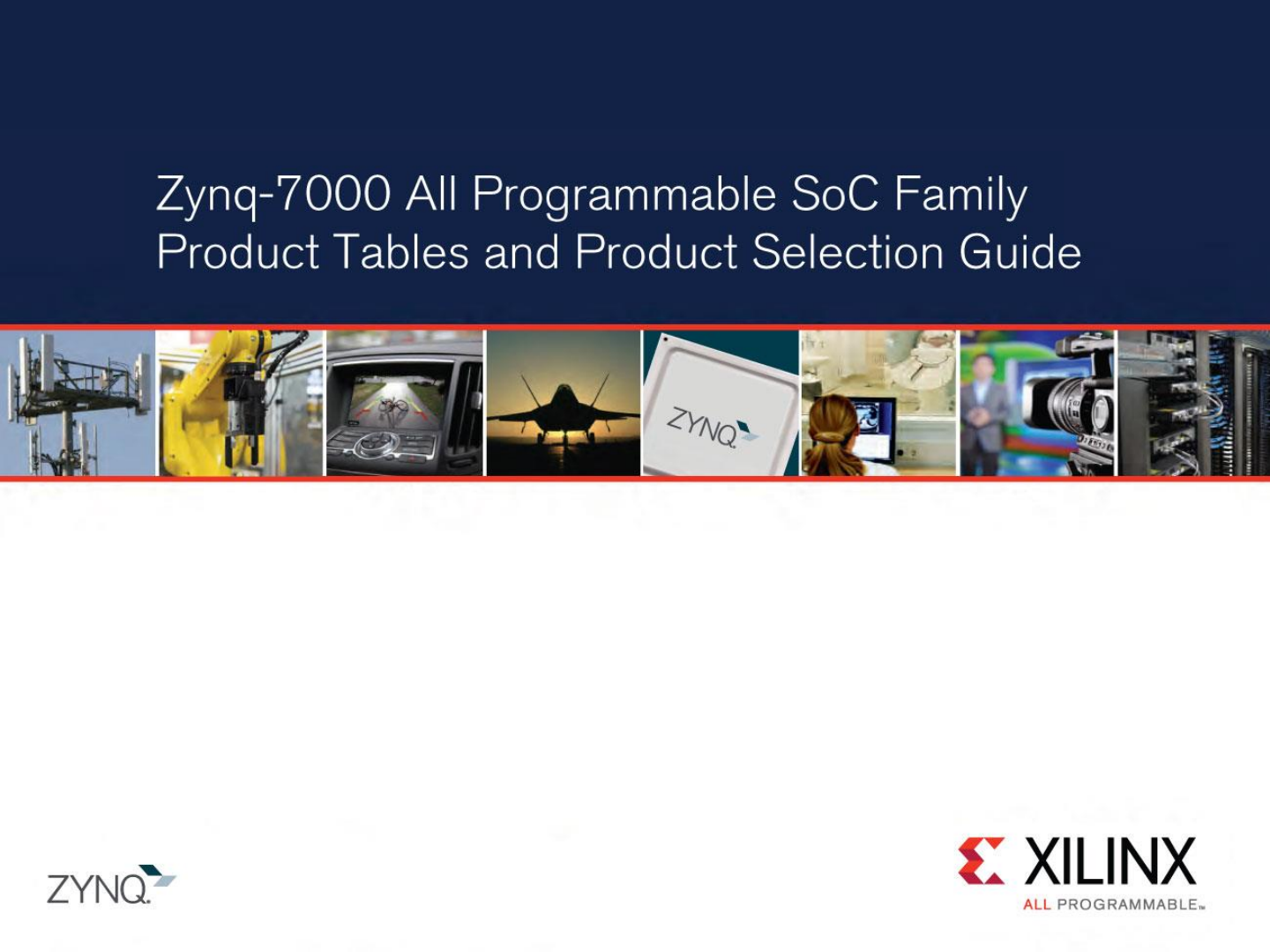
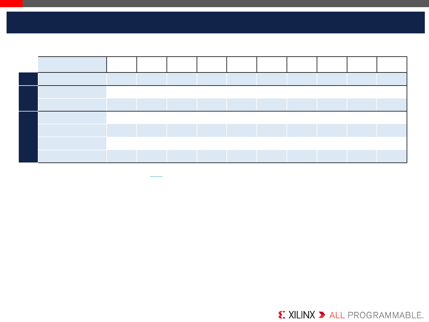
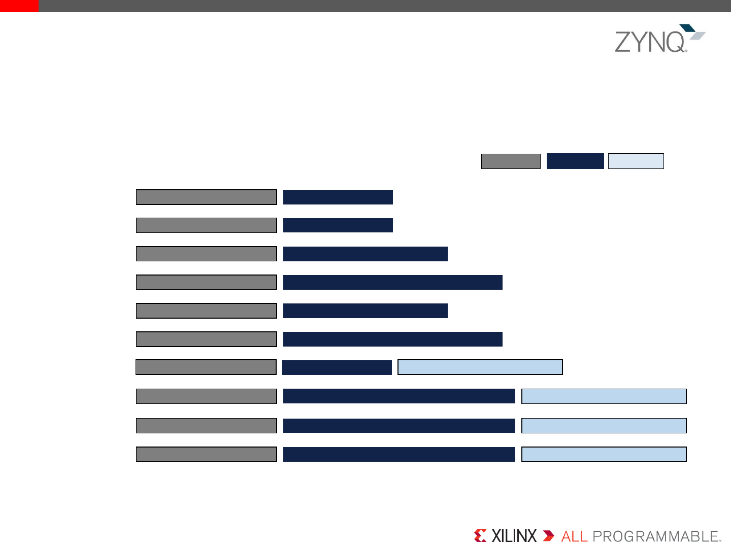
Zynq®-7000 All Programmable SoC Family
Cost-Optimized Devices Mid-Range Devices
Device Name
Z-7007S Z-7012S Z-7014S Z-7010 Z-7015 Z-7020 Z-7030 Z-7035 Z-7045 Z-7100
Part Number
XC7Z007S
XC7Z012S
XC7Z014S
XC7Z010
XC7Z015
XC7Z020
XC7Z030 XC7Z035 XC7Z045 XC7Z100
Processing System (PS)
Processor Core
Single-Core
ARM® Cortex™-A9 MPCore™
Up to 766MHz
Dual-Core ARM
Cortex-A9 MPCore
Up to 866MHz
Dual-Core ARM
Cortex-A9 MPCore
Up to 1GHz(1)
Processor Extensions
NEON™ SIMD Engine and Single/Double Precision Floating Point Unit per processor
L1 Cache
32KB Instruction, 32KB Data per processor
L2 Cache
512KB
On-
Chip Memory
256KB
External Memory Support(2
)
DDR3, DDR3L, DDR2, LPDDR2
External Static Memory Support(2
)
2x Quad-SPI, NAND, NOR
DMA Channels
8 (4 dedicated to PL)
Peripherals
2x UART, 2x CAN 2.0B, 2x I2C, 2x SPI, 4x 32b GPIO
Peripherals w/ built-in DMA
(2)
2x USB 2.0 (OTG), 2x Tri-mode Gigabit Ethernet, 2x SD/SDIO
Security
(3)
RSA Authentication of First Stage Boot Loader,
AES and SHA 256b Decryption and Authentication for Secure Boot
Processing System to
Programmable Logic Interface Ports
(Primary Interfaces & Interrupts Only)
2x AXI 32b Master, 2x AXI 32b Slave
4x AXI 64b/32b Memory
AXI 64b ACP
16 Interrupts
Programmable Logic (PL)
7 Series PL
Equivalent
Artix®-7 Artix-7 Artix-7 Artix-7 Artix-7 Artix-7 Kintex®-7 Kintex-7 Kintex-7 Kintex-7
Logic
Cells
23K 55K 65K 28K 74K 85K 125K 275K 350K 444K
Look-
Up Tables (LUTs)
14,400 34,400 40,600 17,600 46,200 53,200 78,600 171,900 218,600 277,400
Flip-
Flops
28,800 68,800 81,200 35,200 92,400 106,400 157,200 343,800 437,200 554,800
Total Block
RAM
(# 36Kb
Blocks)
1.8Mb
(50)
2.5Mb
(72)
3.8Mb
(107)
2.1Mb
(60)
3.3Mb
(95)
4.9Mb
(140)
9.3Mb
(265)
17.6Mb
(500)
19.1Mb
(545)
26.5Mb
(755)
DSP
Slices
66 120 170 80 160 220 400 900 900 2,020
PCI Express®
—Gen2 x4 — — Gen2 x4 —Gen2 x4 Gen2 x8 Gen2 x8 Gen2 x8
Analog Mixed Signal (AMS) / XADC
(2)
2x 12 bit, MSPS ADCs with up to 17 Differential Inputs
Security
(3)
AES & SHA 256b Decryption & Authentication for Secure Programmable Logic Config
Speed Grades
Commercial
-1 -1 -1 -1
Extended
-2 -2,-3 -2,-3 -2
Industrial
-1, -2 -1, -2, -1L -1, -2, -2L -1, -2, -2L
Notes:
1. 1 GHz processor frequency is available only for -3 speed grades for devices in flip-chip packages. See DS190, Zynq-7000 All Programmable SoC Overview for details.
2. Z-7007S and Z-7010 in CLG225 have restrictions on PS peripherals, memory interfaces, and I/Os. Please refer to UG585, Zynq-7000 All Programmable SoC Technical Reference Manual for more details.
3. Security block is shared by the Processing System and the Programmable Logic.
© Copyright 2014–2016 Xilinx
.
Page 3
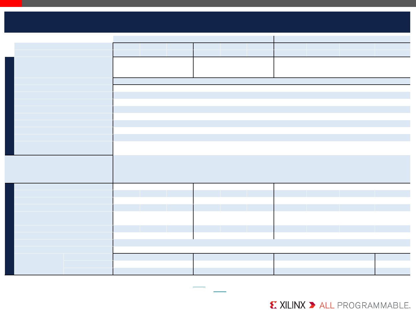
Zynq®-7000 All Programmable SoC Family
HR I/O, HP I/O, PS I/O, and Transceivers (GTP or GTX)
Cost-Optimized Devices Mid-Range Devices
Device Name
Z-7007S Z-7012S Z-7014S Z-7010 Z-7015 Z-7020 Z-7030 Z-7035 Z-7045 Z-7100
Package
Footprint
Dimensions
(mm) (1)
HR I/O, HP I/O
PS I/O(2), GTP Transceivers
HR I/O, HP I/O
PS I/O(2), GTX Transceivers
CLG225 13x13 54, 0
84(3), 0
54, 0
84(3), 0
CLG400 17x17 100, 0
128, 0
125, 0
128, 0
100, 0
128, 0
125, 0
128, 0
CLG484 19x19 200, 0
128, 0
200, 0
128, 0
CLG485(4) 19x19 150, 0
128, 4
150, 0
128, 4
SBG485 / SBV485(4) 19x19 50, 100
128, 4
FBG484 / FBV484 23x23 100, 63
128, 4
FBG676 / FBV676(1) 27x27 100, 150
128, 4
100, 150
128, 8
100, 150
128, 8
FFG676 / FFV676(1) 27x27 100, 150
128, 4
100, 150
128, 8
100, 150
128, 8
FFG900 / FFV900 31x31 212, 150
128, 16
212, 150
128, 16
212, 150
128, 16
FFG1156 / FFV1156 35x35 250, 150
128, 16
Notes:
1.
Devices in the same package are footprint compatible. FBG676 / FBV676 and FFG676 / FFV676 are also footprint compatible.
2.
PS I/O count does not include dedicated DDR calibration pins.
3.
PS DDR and PS MIO pin count is limited by package size. See DS190, Zynq-7000 All Programmable SoC Overview for details.
4.
CLG485 and SBG485 / SBV485 are pin-to-pin compatible. See product data sheets and user guides for more details.
See DS190, Zynq-7000 All Programmable SoC Overview for package details.
© Copyright 2014–2016 Xilinx
.
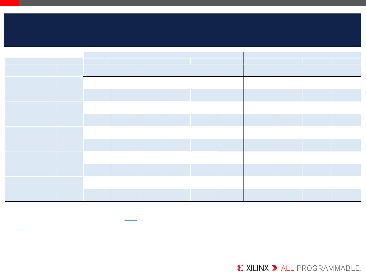
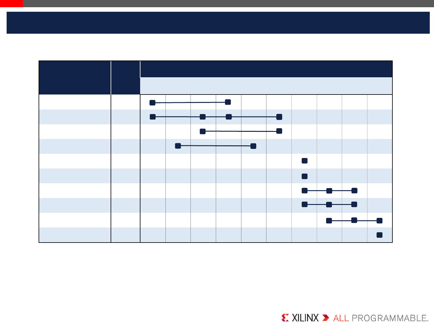
Zynq
®-7000 Device Footprint Compatibility
HR I/O, PS I/O, and GTP Transceivers
PCB
Footprint
Dimensions
(mm)
13x13 17x17 19x19 19x19 23x23 27x27 27x27 31x31 35x35
Unique
Footprint CLG225 CLG400 CLG484 CLG485 FBG484 FBG676 FFG676 FFG900 FFG1156
Z-7007S 54, 84, 0 100, 128, 0
Z-7012S 150, 128, 4
Z-7014S 125, 128, 0 200, 128, 0
Z-7010 54, 84, 0 100, 128, 0
Z-7015 150, 128, 4
Z-7020 125, 128, 0 200, 128, 0
HR I/O, HP I/O, PS I/O, GTX Transceivers
Z-7030 50, 100, 128, 4 100, 63, 128, 4
100, 150, 128, 4
100, 150, 128, 4
Z-7035
100, 150, 128, 8
100, 150, 128, 8
212, 150, 128, 16
Z-7045
100, 150, 128, 8
100, 150, 128, 8
212, 150, 128, 16
Z-7100
212, 150, 128, 16
250, 150, 128, 16
Page 4
13mm–35mm
Important: Verify all data in this document with the device data sheets found at www.xilinx.com
The footprint compatibility range is indicated by shading per column.
© Copyright 2014–2016 Xilinx
.
Page 5
Zynq®-7000 Family Speed Grades
Notes:
1. For full part number details, see the Ordering Information section in DS190, Zynq®-7000 All Programmable SoC Overview.
Available
–Not offered
Device Name(1)
Speed Grade Z-7007S Z-7012S Z-7014S Z-7010 Z-7015 Z-7020 Z-7030 Z-7035 Z-7045 Z-7100
C-1
E
-2
-3 – – – –
I
-1
-2
-1L — — — – – – –
-2L ––––––
C = Commercial (Tj = 0°C to +85°C)
E = Extended (Tj = 0°C to +100°C)
I = Industrial (Tj = –40°C to +100°C)
© Copyright 2014–2016 Xilinx
.
Page 6
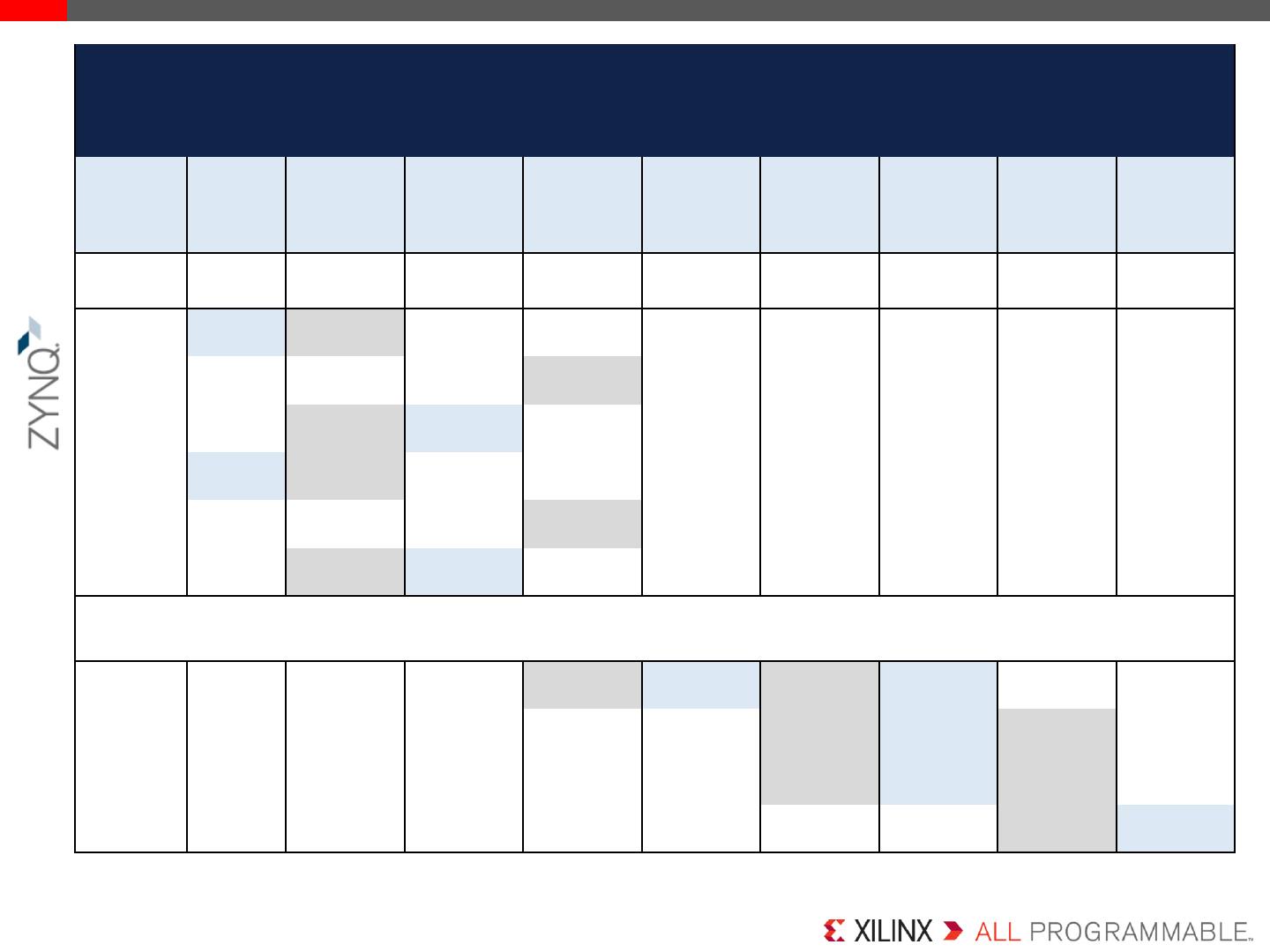
Zynq®-7000 Family
Pkg mm
Z
-
7007S
Z
-
7012S
Z
-
7014S
Z-7010 Z-7015 Z-7020 Z-
7030
Z-7035 Z-7045 Z-7100
CLG225 13 X X
CLG400 17 X X X X
CLG484 19
CLG485 19
SBG485 / SBV485 19
FBG484 / FBV484 23
FBG676 / FBV676 27
FFG676 / FFV676 27
FFG900 / FFV900 31
FFG1156 / FFV1156 35
Zynq®-7000 Family Device Migration Table
© Copyright 2014–2016 Xilinx
.
Page 7
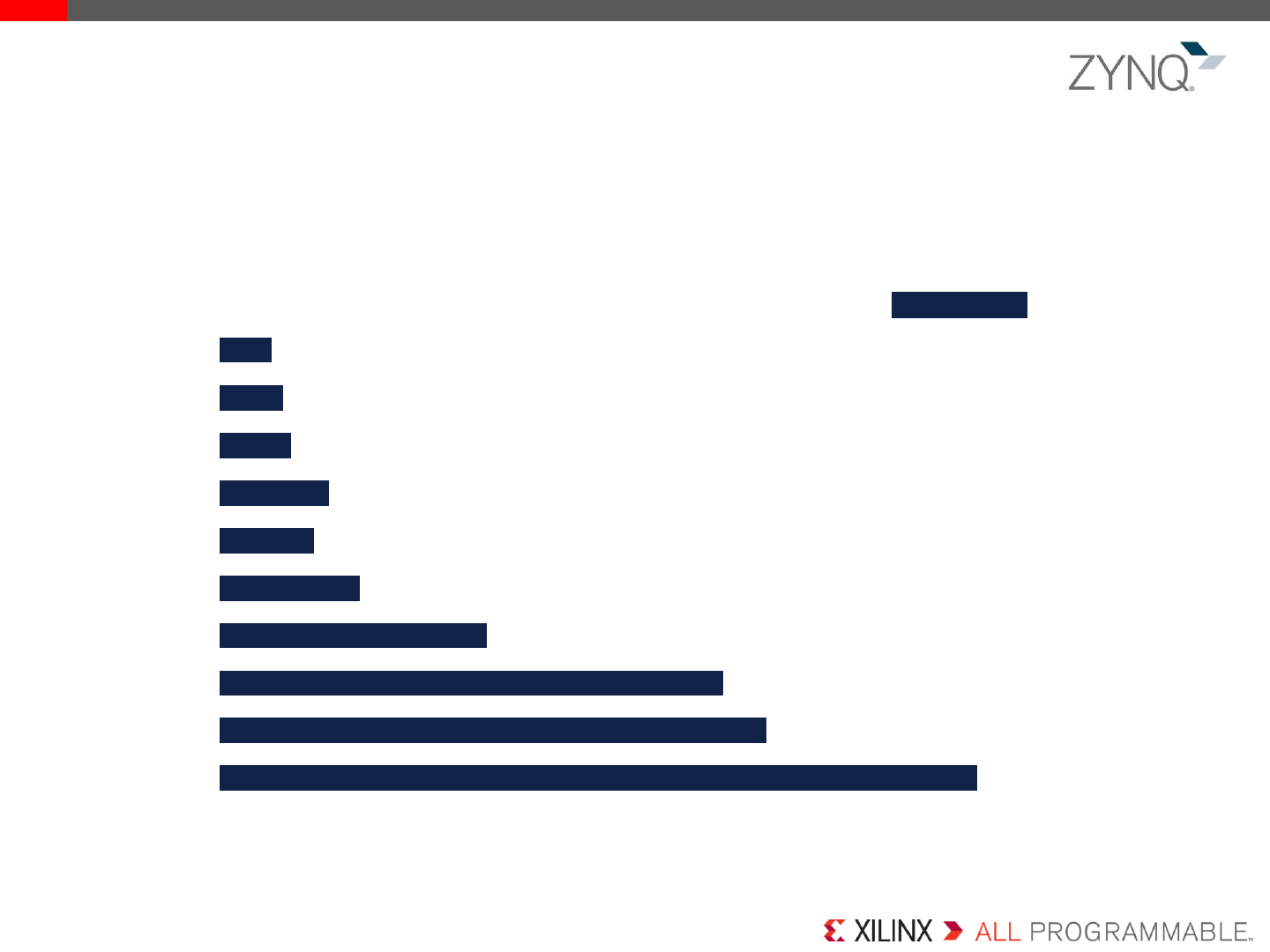
Memory
The Zynq®-7000 family has block RAM (dual-port, programmable, built-in optional error correction), which shares
nothing but stored data.
Important: Verify all data in this document with the device data sheets found at www.xilinx.com
Block RAM
Total Memory (Mb)
Z-7100 26.5
Z-7045 19.1
Z-7035 17.6
Z-7030 9.3
Z-7010 2.1
Z-7015 3.3
Z-7012S 2.5
Z-7014S 3.8
Z-7020 4.9
Z-7007S 1.8
Multiplier = 0.225
© Copyright 2014–2016 Xilinx
.
Transceiver Count and Bandwidth
The serial transceivers in the Zynq-7000 family include the proven on-chip circuits required to provide optimal
signal integrity in real-world environments, at data rates up to 6.25Gb/s (GTP) and 12.5Gb/s (GTX).
Important: Verify all data in this document with the device data sheets found at www.xilinx.com
Total Transceiver Count and Bandwidth GTP GTX
GTP = 6.25Gb/s
GTX = 12.5Gb/s
200Gb/s
Z-7100 16
200Gb/s
Z-7045 16
200Gb/s
Z-7035 16
50Gb/s
Z-7030 4
Z-7007S 0
Z-7014S 0
25Gb/s
Z-7015 4
25Gb/s
Z-7012S 4
Z-7010 0
Z-7020 0
Multiplier = 0.4
Page 8
© Copyright 2014–2016 Xilinx
.
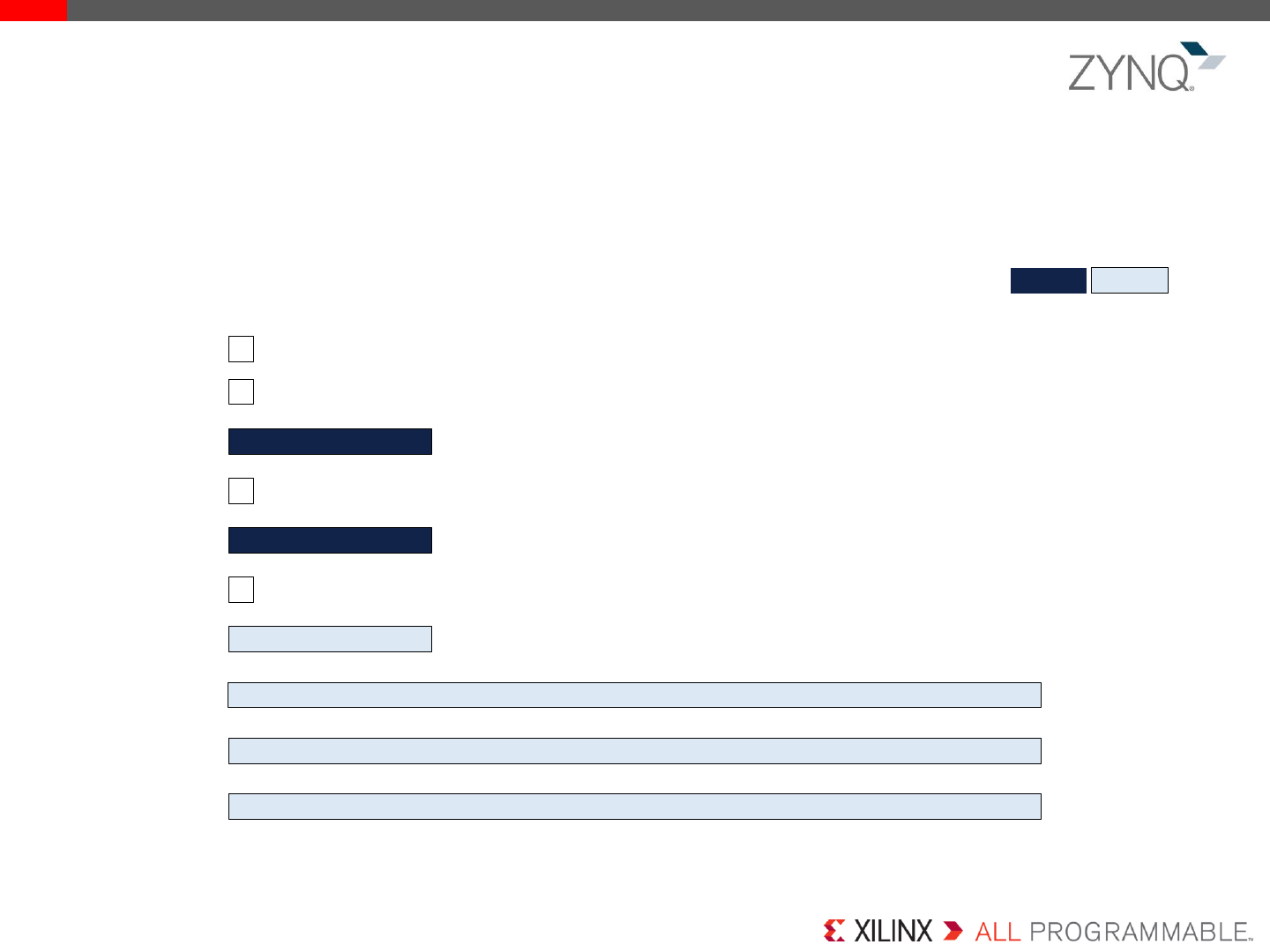
I/O Count
Page 9
Important: Verify all data in this document with the device data sheets found at www.xilinx.com
Maximum I/O Counts
The I/Os are classified as PS I/O, high-range (HR) I/O, and high-performance (HP) I/O. The PS I/Os are composed of
multi-use I/O (MIO), which support 1.8V to 3.3V standards. The HR I/Os are reduced-feature I/Os, providing voltage
support from 1.2V to 3.3V. The HP I/Os are optimized for highest performance operation, from 1.2V to 1.8V.
HR I/O HP I/O
PS I/O
Notes:
1. The PS I/O count is composed of 54 I/Os (excluding DDR interface), which are used to communicate to external components, referred to as multiplexed I/O (MIO).
128
128
128
128
128
128
128
128
128
128
Z-7007S 100
Z-7010 100
Z-7012S 150
Z-7014S 200
Z-7015 150
Z-7020 200
150
Z-7030 100
Z-7035 212
Z-7045 212
Z-7100 212 150
150
150
Multiplier = 0.015
© Copyright 2014–2016 Xilinx
.
Page 10
Zynq®-7000 Family Device Ordering Information
C = Commercial (Tj = 0°C to +85°C)
E = Extended (Tj = 0°C to +100°C)
I = Industrial (Tj = –40°C to +100°C)
Refer to DS190, Zynq-7000 All Programmable SoC Overview for additional information.
Important: Verify all data in this document with the device data sheets found at www.xilinx.com
Xilinx
Commercial
Zynq Value
Index
CL: Wire-bond Molded
(.8mm)
SB: Flip-chip Lidless
(.8mm)
FB: Flip-chip Lidless
(1mm)
FF: Flip-chip Lidded
(1mm)
V: RoHS 6/6
G (CLG) = RoHS 6/6
G (SBG, FBG, FFG) =
RoHS 6/6 with
exemption 15
Speed Grade
-1: Slowest
-L1: Low Power
-2: Mid
-L2: Low Power
-3: Fastest
Temperature
Grade
(C, E, I)
Package
Pin Count
XC Z### -1 FF V### C
Series
7S
Single Core
Indicator
(Z-7007S
Z-7012S
Z-7014S
only)
Footprint
© Copyright 2014–2016 Xilinx
.
DS190, Zynq®-7000 All Programmable SoC Overview
DS187,Zynq-7000 AP SoC (Z-7007S, Z-7012S, Z-7014S, Z-7010, Z-7015, and Z-7020): DC and AC Switching Characteristics
DS191, Zynq-7000 AP SoC (Z-7030, Z-7035, Z-7045, and Z-7100):DC and AC Switching Characteristics
DS176,Zynq-7000 AP SoC and 7 Series Devices Memory Interface Solutions (v4.0)
UG585, Zynq-7000 All Programmable SoC Technical Reference Manual
UG865, Zynq-7000 All Programmable SoC Packaging and Pinout Product Specification
UG471, 7 Series FPGAs SelectIO™ Resources User Guide
UG472,7 Series FPGAs Clocking Resources User Guide
UG473, 7 Series FPGAs Memory Resources User Guide
UG474,7 Series FPGAs Configurable Logic Block User Guide
UG479,7 Series FPGAs DSP48E1 Slice User Guide
UG480, 7 Series FPGAs and Zynq-7000 All Programmable SoC XADC Dual 12-Bit 1 MSPS ADC User Guide
UG482, 7 Series FPGAs GTP Transceivers User Guide
UG821, Zynq-7000 All Programmable SoC Software Developers Guide
UG933, Zynq-7000 All Programmable SoC PCB Design Guide
For a complete list of available documentation, go to: http://www.xilinx.com/products/silicon-devices/soc/zynq-7000.html#documentation
XMP097 (v1.2)
Page 11
Important: Verify all data in this document with the device data sheets found at www.xilinx.com
References
© Copyright 2014-2016 Xilinx, Inc. Xilinx, the Xilinx logo, Artix, ISE, Kintex, Spartan, Virtex, Vivado, Zynq, and other designated brands included herein are trademarks of Xilinx in the United States and other countries. PCI, PCIe, and PCI Express are
trademarks of PCI-SIG and used under license. All other trademarks are the property of their respective owners.
