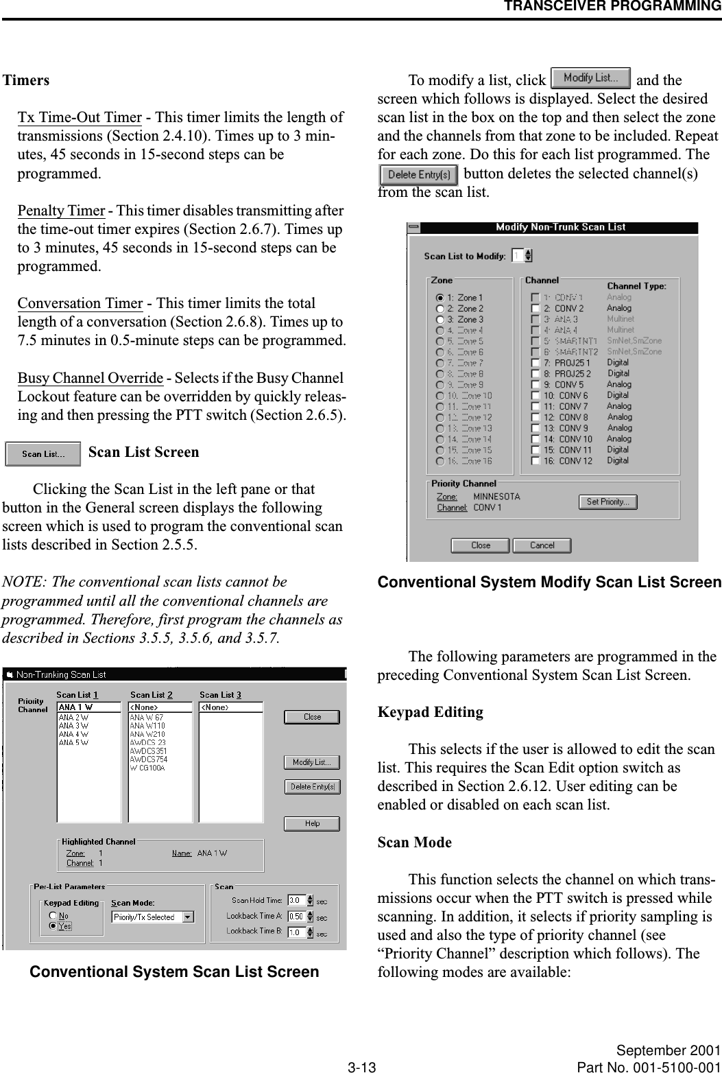
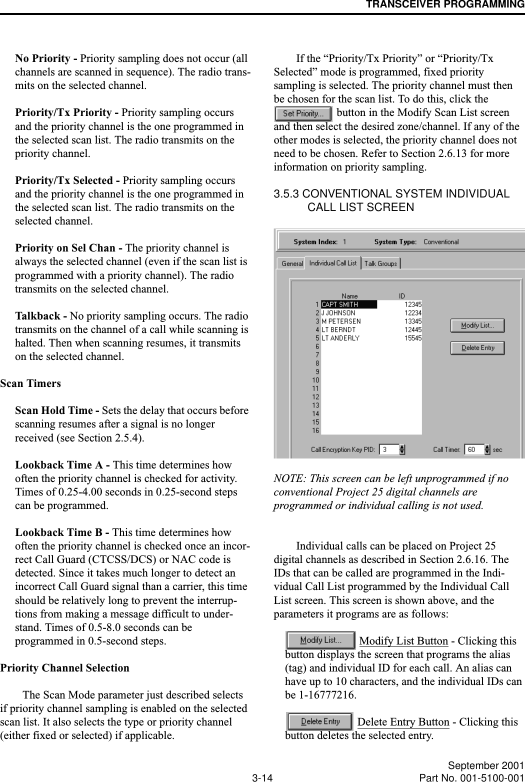
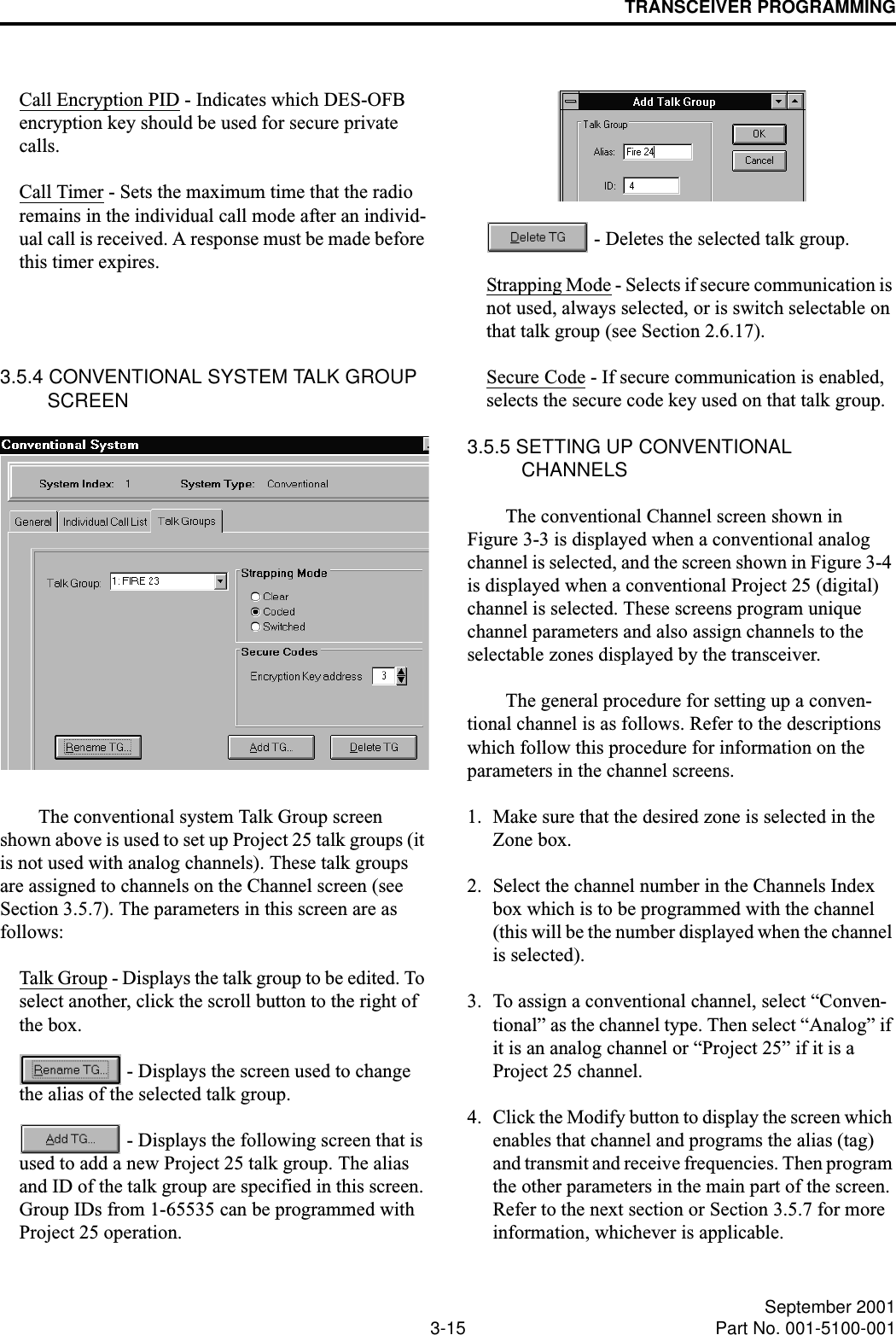
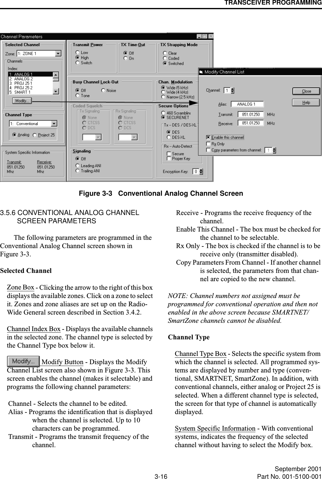
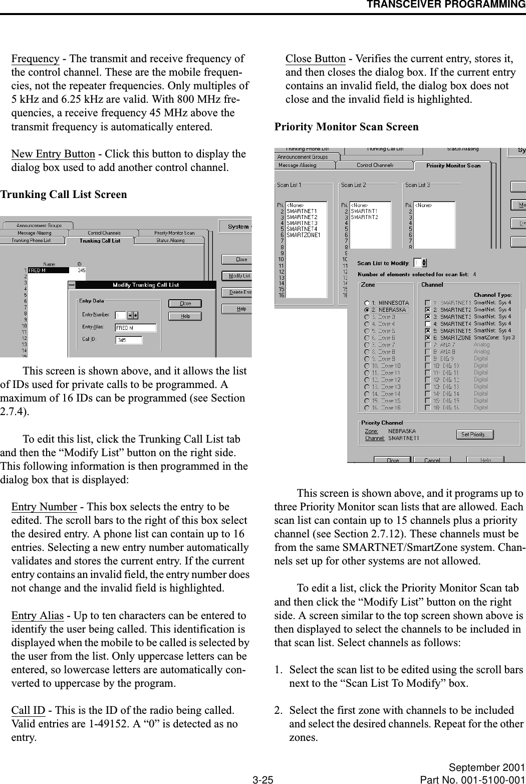
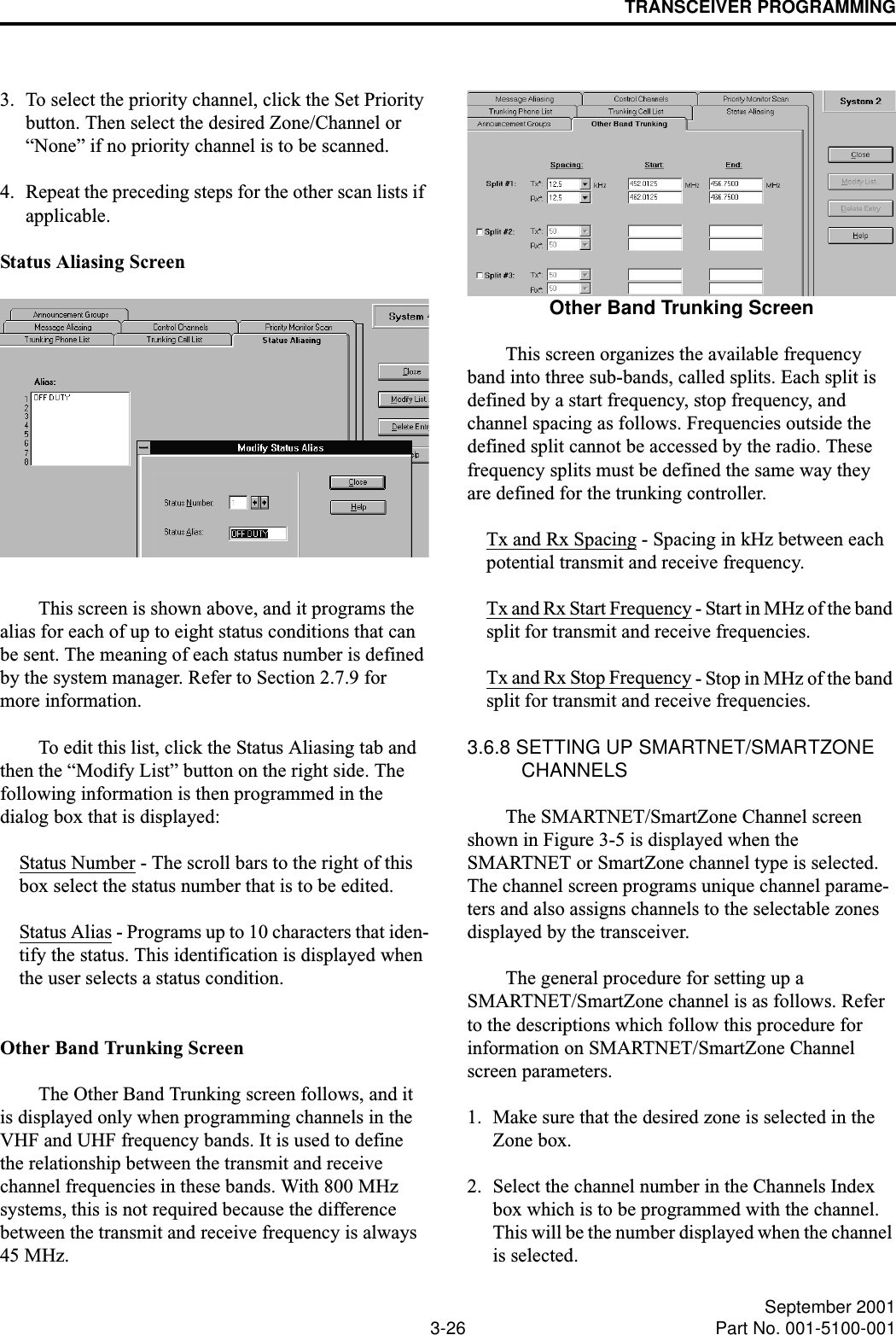
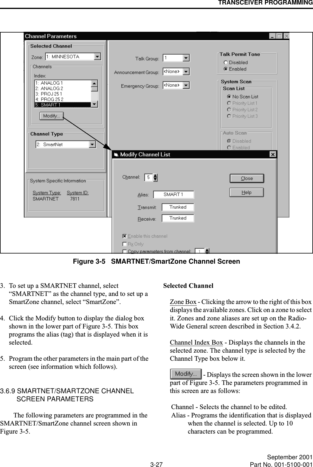
E F Johnson 2425180 PTT 800 MHz SMR User Manual Manual part 2

E. F. Johnson Company PTT 800 MHz SMR Manual part 2

Manual part 2

TRANSCEIVER PROGRAMMING3-13 September 2001Part No. 001-5100-001TimersTx Time-Out Timer - This timer limits the length of transmissions (Section 2.4.10). Times up to 3 min-utes, 45 seconds in 15-second steps can be programmed.Penalty Timer - This timer disables transmitting after the time-out timer expires (Section 2.6.7). Times up to 3 minutes, 45 seconds in 15-second steps can be programmed.Conversation Timer - This timer limits the total length of a conversation (Section 2.6.8). Times up to 7.5 minutes in 0.5-minute steps can be programmed.Busy Channel Override - Selects if the Busy Channel Lockout feature can be overridden by quickly releas-ing and then pressing the PTT switch (Section 2.6.5). Scan List ScreenClicking the Scan List in the left pane or that button in the General screen displays the following screen which is used to program the conventional scan lists described in Section 2.5.5. NOTE: The conventional scan lists cannot be programmed until all the conventional channels are programmed. Therefore, first program the channels as described in Sections 3.5.5, 3.5.6, and 3.5.7.Conventional System Scan List ScreenTo modify a list, click   and the screen which follows is displayed. Select the desired scan list in the box on the top and then select the zone and the channels from that zone to be included. Repeat for each zone. Do this for each list programmed. The  button deletes the selected channel(s) from the scan list.Conventional System Modify Scan List ScreenThe following parameters are programmed in the preceding Conventional System Scan List Screen.Keypad EditingThis selects if the user is allowed to edit the scan list. This requires the Scan Edit option switch as described in Section 2.6.12. User editing can be enabled or disabled on each scan list.Scan ModeThis function selects the channel on which trans-missions occur when the PTT switch is pressed while scanning. In addition, it selects if priority sampling is used and also the type of priority channel (see “Priority Channel” description which follows). The following modes are available:
TRANSCEIVER PROGRAMMING3-14 September 2001Part No. 001-5100-001No Priority - Priority sampling does not occur (all channels are scanned in sequence). The radio trans-mits on the selected channel.Priority/Tx Priority - Priority sampling occurs and the priority channel is the one programmed in the selected scan list. The radio transmits on the priority channel.Priority/Tx Selected - Priority sampling occurs and the priority channel is the one programmed in the selected scan list. The radio transmits on the selected channel.Priority on Sel Chan - The priority channel is always the selected channel (even if the scan list is programmed with a priority channel). The radio transmits on the selected channel. Tal kba ck  - No priority sampling occurs. The radio transmits on the channel of a call while scanning is halted. Then when scanning resumes, it transmits on the selected channel.Scan TimersScan Hold Time - Sets the delay that occurs before scanning resumes after a signal is no longer received (see Section 2.5.4).Lookback Time A - This time determines how often the priority channel is checked for activity. Times of 0.25-4.00 seconds in 0.25-second steps can be programmed.Lookback Time B - This time determines how often the priority channel is checked once an incor-rect Call Guard (CTCSS/DCS) or NAC code is detected. Since it takes much longer to detect an incorrect Call Guard signal than a carrier, this time should be relatively long to prevent the interrup-tions from making a message difficult to under-stand. Times of 0.5-8.0 seconds can be programmed in 0.5-second steps.Priority Channel SelectionThe Scan Mode parameter just described selects if priority channel sampling is enabled on the selected scan list. It also selects the type or priority channel (either fixed or selected) if applicable. If the “Priority/Tx Priority” or “Priority/Tx Selected” mode is programmed, fixed priority sampling is selected. The priority channel must then be chosen for the scan list. To do this, click the  button in the Modify Scan List screen and then select the desired zone/channel. If any of the other modes is selected, the priority channel does not need to be chosen. Refer to Section 2.6.13 for more information on priority sampling.3.5.3 CONVENTIONAL SYSTEM INDIVIDUAL CALL LIST SCREENNOTE: This screen can be left unprogrammed if no conventional Project 25 digital channels are programmed or individual calling is not used. Individual calls can be placed on Project 25 digital channels as described in Section 2.6.16. The IDs that can be called are programmed in the Indi-vidual Call List programmed by the Individual Call List screen. This screen is shown above, and the parameters it programs are as follows: Modify List Button - Clicking this button displays the screen that programs the alias (tag) and individual ID for each call. An alias can have up to 10 characters, and the individual IDs can be 1-16777216. Delete Entry Button - Clicking this button deletes the selected entry.
TRANSCEIVER PROGRAMMING3-15 September 2001Part No. 001-5100-001Call Encryption PID - Indicates which DES-OFB encryption key should be used for secure private calls.Call Timer - Sets the maximum time that the radio remains in the individual call mode after an individ-ual call is received. A response must be made before this timer expires.3.5.4 CONVENTIONAL SYSTEM TALK GROUP SCREENThe conventional system Talk Group screen shown above is used to set up Project 25 talk groups (it is not used with analog channels). These talk groups are assigned to channels on the Channel screen (see Section 3.5.7). The parameters in this screen are as follows: Talk Group - Displays the talk group to be edited. To select another, click the scroll button to the right of the box. - Displays the screen used to change the alias of the selected talk group. - Displays the following screen that is used to add a new Project 25 talk group. The alias and ID of the talk group are specified in this screen. Group IDs from 1-65535 can be programmed with Project 25 operation.  - Deletes the selected talk group.Strapping Mode - Selects if secure communication is not used, always selected, or is switch selectable on that talk group (see Section 2.6.17).Secure Code - If secure communication is enabled, selects the secure code key used on that talk group.3.5.5 SETTING UP CONVENTIONAL CHANNELS The conventional Channel screen shown in Figure 3-3 is displayed when a conventional analog channel is selected, and the screen shown in Figure 3-4 is displayed when a conventional Project 25 (digital) channel is selected. These screens program unique channel parameters and also assign channels to the selectable zones displayed by the transceiver.The general procedure for setting up a conven-tional channel is as follows. Refer to the descriptions which follow this procedure for information on the parameters in the channel screens.1. Make sure that the desired zone is selected in the Zone box. 2. Select the channel number in the Channels Index box which is to be programmed with the channel (this will be the number displayed when the channel is selected).3. To assign a conventional channel, select “Conven-tional” as the channel type. Then select “Analog” if it is an analog channel or “Project 25” if it is a Project 25 channel. 4. Click the Modify button to display the screen which enables that channel and programs the alias (tag) and transmit and receive frequencies. Then program the other parameters in the main part of the screen. Refer to the next section or Section 3.5.7 for more information, whichever is applicable.
TRANSCEIVER PROGRAMMING3-16 September 2001Part No. 001-5100-001Figure 3-3   Conventional Analog Channel Screen3.5.6 CONVENTIONAL ANALOG CHANNEL SCREEN PARAMETERSThe following parameters are programmed in the Conventional Analog Channel screen shown in Figure 3-3.Selected ChannelZone Box - Clicking the arrow to the right of this box displays the available zones. Click on a zone to select it. Zones and zone aliases are set up on the Radio- Wide General screen described in Section 3.4.2.Channel Index Box - Displays the available channels in the selected zone. The channel type is selected by the Channel Type box below it. Modify Button - Displays the Modify Channel List screen also shown in Figure 3-3. This screen enables the channel (makes it selectable) and programs the following channel parameters: Channel - Selects the channel to be edited.Alias - Programs the identification that is displayed when the channel is selected. Up to 10 characters can be programmed. Transmit - Programs the transmit frequency of the channel. Receive - Programs the receive frequency of the channel.Enable This Channel - The box must be checked for the channel to be selectable. Rx Only - The box is checked if the channel is to be receive only (transmitter disabled). Copy Parameters From Channel - If another channel is selected, the parameters from that chan-nel are copied to the new channel.NOTE: Channel numbers not assigned must be programmed for conventional operation and then not enabled in the above screen because SMARTNET/ SmartZone channels cannot be disabled.Channel TypeChannel Type Box - Selects the specific system from which the channel is selected. All programmed sys-tems are displayed by number and type (conven-tional, SMARTNET, SmartZone). In addition, with conventional channels, either analog or Project 25 is selected. When a different channel type is selected, the screen for that type of channel is automatically displayed. System Specific Information - With conventional systems, indicates the frequency of the selected channel without having to select the Modify box.
TRANSCEIVER PROGRAMMING3-17 September 2001Part No. 001-5100-001Transmit PowerThis fixes the transmit power on the channel for the high or low level or allows it to be switch select-able (the Hi/Lo Power option switch is then required). Selectable power is not available with 800 MHz models (Section 2.6.10). Tx Time-OutThis enables or disables the time-out timer on the channel. The time-out timer time is programmed in the conventional system General screen (Section 2.4.10).Busy Channel LockoutOff = disabled, Noise = transmit disallowed if carrier is detected, Tone = transmit allowed only if correct Call Guard code is detected (Section 2.6.5).Coded SquelchThis sets the transmit and receive Call Guard (CTCSS/DCS) coding, if any, used on the channel. If “None” is selected, no code is transmitted and carrier- controlled squelch is used when receiving (Section 2.6.6). The standard Call Guard tones and codes are listed in Table 3-1 located on page 3-29. SignalingOff - No ANI signaling is used.Leading ANI - A DTMF-coded ID is sent at the beginning of each transmission. This ID is set in the radio-wide conventional screen (Section 2.6.15).Trailing ANI - A DTMF-coded ID is sent at the end of each transmission.Channel ModulationThis selects if the channel modulation is wide-band (5 kHz), narrowband (2.5 kHz), or NPSPAC (4 kHz). NPSPAC (public safety) modulation applies to 800 MHz models only.Tx Strapping ModeNOTE: See Section 2.6.17 for more information. Clear - All transmissions on the channel occur in the clear (unscrambled) mode.Coded - All transmissions on the channel occur in the secure (scrambled) mode selected by Coded Options.Switched - The clear or secure status of the channel is selected by the Clear/Secure option switch.Secure OptionsThese options select either the Transcrypt 460 or SecureNet™ DES type of secure communication when either the coded or switched strapping mode is selected.Tx DES/DES-XL - Selects either DES or DES-XL encryption protocol. Rx AutoDetect - With the SecureNet protocol, select-ing “Secure” enables automatic detection of encrypted receive signals. This may increase the response time of the radio to an incoming signal. Selecting “Proper Key” causes the radio to search the available SecureNet keys until it finds a match for the current transmission. Encryption Key - Selects the encryption key from 0-15 that is used on the channel. This refers to the hardware location in the radio of the real key.
TRANSCEIVER PROGRAMMING3-18 September 2001Part No. 001-5100-001Figure 3-4   Conventional Project 25 Digital Channel Screen3.5.7 CONVENTIONAL PROJECT 25 (DIGITAL) CHANNEL SCREEN PARAMETERSThe following parameters are programmed in the conventional Project 25 digital channel screen shown in Figure 3-4. Refer to Section 2.6.16 for more infor-mation on Project 25 operation.The Selected Channel, Channel Type, Transmit Power, and Transmit Time-Out Parameters are programmed the same as with analog channels described in preceding section.Talk GroupsThis selects the Project 25 talk group that is assigned to the channel. The talk group programs the talk group ID, strapping mode, and encryption key address. Talk groups for Project 25 channels are programmed in the Conventional System Talk Group screen described in Section 3.5.4.Strapped to Selected Group - If this parameter is selected, the talk group on that channel is always the selected talk group and cannot be changed.Radio List Selectable - If this parameter is selected, the talk group may be changed by the radio operator using the (Digital) Talk Group Select option switch.Busy Channel LockoutOff = disabled, Noise = transmit disallowed if carrier is detected, NAC = transmit allowed only if correct NAC is detected (Section 2.6.5).Access CodesPrograms the transmit and receive NAC (Network Access Code). These codes can be 0-4095. Refer to Section 2.6.16 for more information.Mixed ModeA mixed mode that allows both analog and Project 25 operation to be programmed on a channel can be enabled on the Project 25 channel screen (see Figure 3-4). This mode is programmed as follows:Enable - Checking this box selects mixed analog/Project 25 operation on the channel.Tx Analog - Checking this box selects Transmit = analog/Receive = Project 25. If it is not checked, the opposite is selected.When the mixed mode is selected, the channel modulation, coded squelch, and ANI signaling param-eters for the analog channel must then be programmed.
TRANSCEIVER PROGRAMMING3-19 September 2001Part No. 001-5100-001These parameters are programmed the same as described in Section 3.5.6.3.6 PROGRAMMING SMARTNET/SMARTZONE SYSTEMS AND CHANNELS3.6.1 INTRODUCTIONTo program SMARTNET and SmartZone systems and channels, proceed as follows: 1. Program the SMARTNET/SmartZone radio-wide information as described in Section 3.4. 2. To create a new SMARTNET/SmartZone system, select the Systems > Add Systems in the menu bar (see Section 3.1.11). Up to sixteen systems of any type can be programmed as described in Section 1.2.5.3. Program the SMARTNET/SmartZone system infor-mation as described starting in the next section. Make sure the desired SMARTNET or SmartZone system is displayed by clicking it in the left pane or selecting it in the Window menu in the menu bar (see Section 3.1.9). Then program the channels as described starting in Section 3.6.8. 3.6.2 SMARTNET/SMARTZONE SYSTEM GENERAL SCREENThe preceding SMARTNET/SmartZone System General screen programs the following parameters:Restricted AccessChange System ID Button - Displays the Change System ID screen which is used to enter the system ID of the system. This ID is entered as a hexadecimal number from 0-9 and A-F. Valid numbers are from 0001-FFFF. The system ID corresponding to the desired ID must also be located in the “key” subdi-rectory of the program file.System ID - Read-only field which shows the ID of the system currently being edited.Splinter ChannelsWhen splinter channels are enabled, the receive and transmit frequencies are 12.5 kHz lower than the normal frequencies. Splinter channels are used only as required in the Mexico and Canada border areas for frequencies between 806 and 820.975 MHz.Channel ModulationWhen “Wideband” is enabled, the radio operates with a 4 kHz maximum deviation between 821.000 and 824.975 MHz and 5 kHz maximum deviation for all other frequencies. When it is disabled, deviation is 5 kHz with all frequencies.System Lists ButtonThis button displays the screens used to program the various per system lists. Refer to Section 3.6.7 for more information on these lists.Dynamic RegroupingEnable For This System - When this box is checked, a dynamic regrouping channel is enabled. This is a SMARTNET channel which has the corresponding talk group dynamically set by the dispatcher.Zone - The physical zone containing the dynamic regrouping channel. The value is selected on the Channel Parameters screen.
TRANSCEIVER PROGRAMMING3-20 September 2001Part No. 001-5100-001Channel - The physical channel used for dynamic regrouping. The value is selected on the Channel Parameters screen.Affiliation TypeAutomatic - The radio immediately affiliates with the central controller as soon as it is turned on and auto-matically re-affiliates each time the talk group is changed.On PTT - The radio affiliates with the central control-ler only when the PTT switch is pressed.Time-Out TimerThis programs the time-out timer setting for the system. It can be programmed for 0 min, 15 sec up to 3 min, 45 sec or it can be disabled (see Section 2.4.10).ISW DelayIncreasing or decreasing this value changes the transmission timing of ISWs relative to the reception of OSWs.3.6.3 SMARTNET/SMARTZONE SYSTEM OTHER ID’S SCREENThe SMARTNET/SmartZone Other ID’s screen is shown above, and it programs the following parameters.Individual ID - Uniquely identifies the radio on a par-ticular system. Each radio must have a different Unit ID. Valid Unit IDs are from 1-63535.Connect Tone - The tone expected by the controller on the traffic channel to verify that a subscriber trans-mission is occurring. This tone should be set the same as it is in the controller.Encryption Key IDsPrograms SecureNet Encryption ID selection that is used in all except group calls.System Wide - Key used for system-wide calls(typically originated by the dispatcher).Failsoft - Key used in failsoft conditions (see Section 2.7.11).Patch Key Select - Key used in patch calls.Unit To Unit - Key used for unit-to-unit (private) calls.Interconnect - Key used for telephone interconnect calls.Dynamic Talk Group - Key used for the dynamic regrouping talk group when it is a standard talk group.Dynamic Ann. Group - Key used for the dynamic regrouping talk group when it is an announcement group.3.6.4 SMARTNET/SMARTZONE SYSTEM PHONE INTERCONNECT SCREENThe SMARTNET/SmartZone Phone Intercon-nect screen follows on the next page, and it programs the following parameters.Phone InterconnectRefer to Section 2.7.6 for more information on telephone calls.Disabled - Telephone calls cannot be placed or received.
TRANSCEIVER PROGRAMMING3-21 September 2001Part No. 001-5100-001Answer Only - Telephone calls can be received but not placed.List Only - Telephone calls can be placed and received, and numbers can be recalled from memory only.Unlimited - Telephone calls can be placed and received, and numbers can be recalled from memory or dialed using a microphone keypad.SMARTNET/SmartZone Phone Interconnect ScreenPrivate CallThis is the same as above, except for private (unit-to-unit) calls. Refer to Section 2.7.4 for more information.Private Call IIThis programs either standard or enhanced private calls as follows:Standard - The user does not receive any feedback when the called radio is not active in the system. Only a “No Answer” is received if the called radio does not answer.Enhanced - When a call is placed, the system tells the user if the called radio is currently active in the sys-tem and within range. The calling radio displays “No Ack” if the called radio is not active in the system and “No Answer” if it is active but does not answer.Phone DTMF TimingInitial Delay - Delay from 50-500 milliseconds from when a traffic channel is granted for phone intercon-nect to the start of the dialing out of the phone number.Digit Duration - Duration from 50-500 milliseconds of each phone number digit.Inter-Digit Delay - Delay from 50-500 milliseconds between each digit of a phone number. start here3.6.5 SMARTNET/SMARTZONE SYSTEM TALK GROUPS SCREENThe SMARTNET/SmartZone Talk Groups screen shown above is used to set up SMARTNET/SmartZone talk groups and program unique talk group information. The parameters programmed in this screen are as follows: Talk Group - Selects the talk group to program. This is the actual ID of the talk group. Talk groups are added or deleted by clicking the Add TG or Delete TG button (see following). Talk groups are assigned to channels on the channel screen (see Section 3.6.9). - Clicking this button displays a dialog box that adds a new talk group. The alias (alpha tag) of up to ten characters is entered, and the new group is then added after the others that are already set up.
TRANSCEIVER PROGRAMMING3-22 September 2001Part No. 001-5100-001Each SMARTNET/SmartZone system can be pro-grammed with up to 256 talk groups. - Clicking this button deletes the cur-rently selected talk group (the one displayed in the “Talk Group” box).Failsoft ChannelEnable - Enables a failsoft channel on the talk group if a controller failure occurs (see Section 2.7.11).Disable - The failsoft mode is not entered if the con-troller fails.Tx/Rx Frequency - Programs the failsoft channel frequency if “Enabled” is checked.Analog/Project 25This selects the type of SMARTNET/SmartZone channel as analog or Project 25 (digital).Strapping ParametersThe Strapping Parameters program the channel type (analog or Project 25 digital) and encryption on the talk group as follows:Clear Mode - All transmissions on the talk group occur in the clear (unscrambled) mode. Coded Mode - All transmissions on the talk group occur in the secure (scrambled) mode selected as follows.Switched Mode - The clear or secure status of the talk group is selected by the Clear/Secure option switch.NOTE: Refer to Section 2.7.15 for more SMARTNET/SmartZone encryption information. 460 Scrambling/SecureNet Mode - These options select either the Transcrypt 460 or DES type of secure communication when either the coded or switched strapping mode is selected.Tx DES/DES-XL - Selects either DES or DES-XL encryption protocol.Rx Secure Autodetect - With the SecureNet protocol, selecting “Secure” enables automatic detection of encrypted receive signals. This may increase the response time of the radio to an incoming signal. Selecting “Proper Key” causes the radio to search the available SecureNet keys until it finds a match for the current transmission.Encryption Key - Selects the encryption key used on the talk group. This is a number from 0-15 that refers to a hardware location in the radio that contains the real key.3.6.6 SMARTNET/SMARTZONE SYSTEM EMERGENCY SETTINGS SCREENThe SMARTNET/SmartZone Emergency Settings screen and the parameters programmed in this screen are as follows: Emergency CallEnable - When the Emergency option switch and then the PTT switch are pressed, an emergency group call is transmitted.Disable - An emergency group call is not authorized.Emergency Hot MicEnable - When an emergency alarm is generated and the emergency alarm acknowledgment received, the emergency mode is automatically entered and trans-mitting begins for the time specified by the Tx Period parameter (see following).Disable - Automatic transmissions do not occur.
TRANSCEIVER PROGRAMMING3-23 September 2001Part No. 001-5100-001Tx Period - Defines the period during which trans-missions occur with the microphone audio unmuted (without user intervention). Times of 10-120 seconds in 10-second steps can be selected.Emergency AlarmDisabled - No emergency signal is sent when the user presses the Emergency option switch.Normal - When the user presses the Emergency option switch, an emergency signal is sent to the dis-patcher. Audio and visual feedback is provided by the radio.Silent - Same as “Normal” except no audio or visual feedback is provided.Retry Counter - When “Unlimited” is selected, an emergency call is repeated until acknowledged or canceled. When “Limited” is checked, calls are attempted only the specified number of times.3.6.7 SMARTNET/SMARTZONE SYSTEM LISTS SCREENSClicking System Lists in the left pane under SMARNET > General or the   button in the General screen described in Section 3.6.2 displays the screens used to program the various lists that are unique for each SMARTNET/SmartZone system. These screens are as follows:Trunking Phone List ScreenThis screen programs the phone number list if used (see Section 2.7.6). To edit this list, click the Trunking Phone List tab and then the “Modify List” button on the right side of the screen. The following information is then programmed in the dialog box that is displayed:Entry Number - This box selects the entry to be edited. The scroll bars to the right of this box select the desired entry. A phone list can contain up to 16 entries. Selecting a new entry number automatically validates and stores the current entry. If the current entry contains an invalid field (for example, too many digits in the phone number), the entry number does not change and the invalid field is highlighted.Entry Alias - Up to ten characters can be entered to identify the phone number. This identification is dis-played when phone numbers are selected by the user from the list. Only uppercase letters can be entered, so lowercase letters are automatically converted to uppercase by the program.Phone Number - This is the number dialed when the location is selected. Characters that can be entered include 0-9, #, (,), and P (a “P” programs a pause). The maximum number of digits excluding (,) and spaces is 16, and the maximum including (,) and spaces is 24.Close - Clicking this button verifies the current entry, stores it, and then closes the dialog box. If the current entry contains an invalid field, the dialog box does not close and the invalid field is highlighted.Help - Accesses the Help screen. Help can also be selected at any time by pressing the F1 key.Message Aliasing ScreenThis screen associates an alias (name) with each message number (see Section 2.7.8). To edit this list,
TRANSCEIVER PROGRAMMING3-24 September 2001Part No. 001-5100-001click the Message Aliasing tab and then the “Modify List” button on the right side. The following informa-tion is then programmed in the dialog box that is displayed:Message Number - This box selects the message to be edited. The scroll bars to the right of this box select the desired message number. Message Alias - Programs the alias which can be up to any ten alphanumeric characters.Close Button - Validates the entry and closes the dia-log box. The entry is also validated when another message number is selected.Announcement Groups ScreenThis screen programs the announcement groups that are used to communicate with several talk groups simultaneously. There can be up to 3 announcement groups per system, and each announcement group can have up to 15 talk groups. To create an announcement group, click the “Add AG” button and the “Add TGs to the AG” screen also shown above is displayed. Enter the announcement group ID, click the talk groups to select/deselect those that are to be included, and then create the announce-ment group by clicking the “Create AG” button. To delete the current announcement group, click the “Delete AG” button.To edit an announcement group, click the “Modify List” button and select the announcement group to be edited from the “AG” pull-down menu. Then click the talk groups to select/de-select them and then click the “Update List” button to make the changes.Main Screen ParametersTalk Groups - This is a read-only list of all talk groups currently in the announcement group.Analog/Project 25 - Programs the type of communi-cation associated with the announcement group. Either analog or digital (Project 25) communication can be selected.Security - Defines the type of secure communication used, if any, for the announcement group. These parameters are programmed similar to those on the Talk Group screen described in Section 3.6.5. Control Channels ScreenThis screen allows the system manager to view and edit the control channels. Each SMARTNET system can have up to four control channels, and each SmartZone system can have up to 32 control channels. Only one control channel is active at a time. To edit this list, click the Control Channels tab and then the “Modify List” button on the right side. The following information is then programmed in the dialog box that is displayed:Control Channel - Selects the control channel to be edited. To add a new channel, click the “New Entry” button.
TRANSCEIVER PROGRAMMING3-25 September 2001Part No. 001-5100-001Frequency - The transmit and receive frequency of the control channel. These are the mobile frequen-cies, not the repeater frequencies. Only multiples of 5 kHz and 6.25 kHz are valid. With 800 MHz fre-quencies, a receive frequency 45 MHz above the transmit frequency is automatically entered.New Entry Button - Click this button to display the dialog box used to add another control channel.Trunking Call List ScreenThis screen is shown above, and it allows the list of IDs used for private calls to be programmed. A maximum of 16 IDs can be programmed (see Section 2.7.4). To edit this list, click the Trunking Call List tab and then the “Modify List” button on the right side. This following information is then programmed in the dialog box that is displayed:Entry Number - This box selects the entry to be edited. The scroll bars to the right of this box select the desired entry. A phone list can contain up to 16 entries. Selecting a new entry number automatically validates and stores the current entry. If the current entry contains an invalid field, the entry number does not change and the invalid field is highlighted.Entry Alias - Up to ten characters can be entered to identify the user being called. This identification is displayed when the mobile to be called is selected by the user from the list. Only uppercase letters can be entered, so lowercase letters are automatically con-verted to uppercase by the program.Call ID - This is the ID of the radio being called. Valid entries are 1-49152. A “0” is detected as no entry. Close Button - Verifies the current entry, stores it, and then closes the dialog box. If the current entry contains an invalid field, the dialog box does not close and the invalid field is highlighted.Priority Monitor Scan ScreenThis screen is shown above, and it programs up to three Priority Monitor scan lists that are allowed. Each scan list can contain up to 15 channels plus a priority channel (see Section 2.7.12). These channels must be from the same SMARTNET/SmartZone system. Chan-nels set up for other systems are not allowed. To edit a list, click the Priority Monitor Scan tab and then click the “Modify List” button on the right side. A screen similar to the top screen shown above is then displayed to select the channels to be included in that scan list. Select channels as follows:1. Select the scan list to be edited using the scroll bars next to the “Scan List To Modify” box.2. Select the first zone with channels to be included and select the desired channels. Repeat for the other zones.
TRANSCEIVER PROGRAMMING3-26 September 2001Part No. 001-5100-0013. To select the priority channel, click the Set Priority button. Then select the desired Zone/Channel or “None” if no priority channel is to be scanned.4. Repeat the preceding steps for the other scan lists if applicable.Status Aliasing ScreenThis screen is shown above, and it programs the alias for each of up to eight status conditions that can be sent. The meaning of each status number is defined by the system manager. Refer to Section 2.7.9 for more information. To edit this list, click the Status Aliasing tab and then the “Modify List” button on the right side. The following information is then programmed in the dialog box that is displayed:Status Number - The scroll bars to the right of this box select the status number that is to be edited. Status Alias - Programs up to 10 characters that iden-tify the status. This identification is displayed when the user selects a status condition.Other Band Trunking ScreenThe Other Band Trunking screen follows, and it is displayed only when programming channels in the VHF and UHF frequency bands. It is used to define the relationship between the transmit and receive channel frequencies in these bands. With 800 MHz systems, this is not required because the difference between the transmit and receive frequency is always 45 MHz. Other Band Trunking ScreenThis screen organizes the available frequency band into three sub-bands, called splits. Each split is defined by a start frequency, stop frequency, and channel spacing as follows. Frequencies outside the defined split cannot be accessed by the radio. These frequency splits must be defined the same way they are defined for the trunking controller.Tx and Rx Spacing - Spacing in kHz between each potential transmit and receive frequency.Tx and Rx Start Frequency - Start in MHz of the band split for transmit and receive frequencies.Tx and Rx Stop Frequency - Stop in MHz of the band split for transmit and receive frequencies.3.6.8 SETTING UP SMARTNET/SMARTZONE CHANNELS The SMARTNET/SmartZone Channel screen shown in Figure 3-5 is displayed when the SMARTNET or SmartZone channel type is selected. The channel screen programs unique channel parame-ters and also assigns channels to the selectable zones displayed by the transceiver.The general procedure for setting up a SMARTNET/SmartZone channel is as follows. Refer to the descriptions which follow this procedure for information on SMARTNET/SmartZone Channel screen parameters.1. Make sure that the desired zone is selected in the Zone box. 2. Select the channel number in the Channels Index box which is to be programmed with the channel. This will be the number displayed when the channel is selected.
TRANSCEIVER PROGRAMMING3-27 September 2001Part No. 001-5100-001Figure 3-5   SMARTNET/SmartZone Channel Screen3. To set up a SMARTNET channel, select “SMARTNET” as the channel type, and to set up a SmartZone channel, select “SmartZone”.4. Click the Modify button to display the dialog box shown in the lower part of Figure 3-5. This box programs the alias (tag) that is displayed when it is selected.5. Program the other parameters in the main part of the screen (see information which follows). 3.6.9 SMARTNET/SMARTZONE CHANNEL SCREEN PARAMETERSThe following parameters are programmed in the SMARTNET/SmartZone channel screen shown in Figure 3-5.Selected ChannelZone Box - Clicking the arrow to the right of this box displays the available zones. Click on a zone to select it. Zones and zone aliases are set up on the Radio- Wide General screen described in Section 3.4.2.Channel Index Box - Displays the channels in the selected zone. The channel type is selected by the Channel Type box below it. - Displays the screen shown in the lower part of Figure 3-5. The parameters programmed in this screen are as follows:Channel - Selects the channel to be edited.Alias - Programs the identification that is displayed when the channel is selected. Up to 10 characters can be programmed.
TRANSCEIVER PROGRAMMING3-28 September 2001Part No. 001-5100-001Transmit - Not programmable because the transmit frequency is dynamically assigned over the air (“Trunked” is always displayed).Receive - Dynamically assigned like the preceding transmit frequency.Enable This Channel - Not used because SMART-NET/SmartZone channels are always enabled if set up. To disable a channel so that it is not selectable, choose the conven-tional type and do not check this box.Copy Parameters From Channel - If another channel is selected in the box, the parameters from that channel are copied to the new channel.Channel TypeChannel Type Box - Selects the specific system from which the channel is selected. All programmed systems are displayed by number and type (conven-tional, SMARTNET, SmartZone). When a different channel type is selected, the screen for that type of channel is automatically displayed. Other Screen ParametersSystem Specific Information - With SMARTNET/SmartZone systems, indicates the system ID programmed on the system General screen (seeSection 3.6.2).Talk Group - Selects the talk group selected by that channel. Talk groups are programmed in the Talk Group screen described in Section 3.6.5.Announcement Group - Selects one of up to three announcement groups selected by the channel. Refer to “Announcement Group Screen” in Section 3.6.7 for more information.Emergency Group - Selects the talk group used for emergency calls.Talk Permit Tone - When enabled, a short tone sounds after a request for a group call has been approved by the main controller. This indicates that speaking can begin. When disabled, no audio feed-back is used to indicate when speaking can begin.System Scan - Selects the Priority Monitor Scan list selected by the channel (see “Priority Monitor Scan Screen” description in Section 3.6.7). If “No Scan List” is programmed, scanning is not selectable on that channel.Auto Scan - When enabled and a channel is selected, the radio automatically begins scanning the scan list associated with that channel. When disabled, scan-ning can only be started manually by the Scan option switch.3.7 PASSWORD OPERATION3.7.1 GENERALThe 50xx portable radio can be programmed with a Power-Up and Programming password. If the Power-Up password is enabled, it must be entered each time power is turned on to make the radio operational. This prevents unauthorized use. The Programming pass-word must be entered to access the keypad program-ming feature of the radio. This prevents unauthorized reprogramming of the transceiver. Currently, the 50xx portable is the only transceiver that is programmed with the PCTrunk software that utilizes password access. More information on these two passwords follows.3.7.2 POWER-UP PASSWORDThe Power-Up password function is enabled on the Radio-Wide General screen described in Section 3.4.2. This password must then be entered each time transceiver power is turned on. In addition, since the radio resets after downloading or uploading data, it must be entered after performing those functions (see Sections 3.3.3 and 3.3.4). When entering the pass-word using the radio keypad, enter the eight password digits and then press the ENT key. If an error is made, press the CLR key to start over.To enable the power-up password function on the programmer screen, the Power-Up password must be entered. This prevents the radio from being programmed with an unknown password which would make it inoperable. The password is a series of eight numbers, and it is programmed by clicking the “Change Password” button on the Radio-Wide General screen. The default password is eight zeros (00000000), and it may need to be entered as the “old” password if applicable. The password can also be
TRANSCEIVER PROGRAMMING3-29 September 2001Part No. 001-5100-001changed using the radio keypad when the keypad is locked by entering the old password and then pressing the # key. Refer to Section 2.4.3 for more information.If the Power-Up password has been enabled in the radio connected to the programmer, the Programming password described in the next section must then be entered before a data can be downloaded or uploaded. This prevents an unauthorized person from reading radio data or changing radio programming.If the password is forgotten, it can be overridden by pressing the lower button on the side 8 times. This unlocks the radio and reverts to the default password of “00000000”. However, it also erases all channel frequencies, trunked group IDs, and encryption infor-mation. Therefore, the radio must be reprogrammed after this is done to make it operational again.3.7.3 PROGRAMMING PASSWORDThe Programming password must be entered to enable the Keypad Programming mode described in Section 2.9. This prevents an unauthorized person from changing the radio programming. As described in the preceding section, the Programming password must also be entered when downloading or uploading data from a radio that has the Power-Up password function enabled.Table 3-1   Call Guard (CTCSS/DCS) Codes and TonesRecommended Tone Call Guard CodesCode Freq Code Freq Code Freq Code Freq Code Freq09 91.5 18 123.0 27 167.9 37* 241.801 67.0 10 94.8 19 127.3 28 173.8 38* 250.302 71.9 11** 97.4 20 131.8 29 179.9 39** 69.303 74.4 12 100.0 21 136.5 30 186.2 40** 206.504 77.0 13 103.5 22 141.3 31 192.8 41** 229.105 79.7 14 107.2 23 146.2 32 203.5 42** 254.106 82.5 15 110.9 24 151.4 33 210.707 85.4 16 114.8 25 156.7 34* 218.108 88.5 17 118.8 26 162.2 35* 225.7* These tones normally are not used because of their close proximity to the voice frequencies** This tone is normally not used because it may cause interference with adjacent tones.Recommended Digital Call Guard Codes023 065 131 172 261 346 431 532 654 743025 071 132 174 263 351 432 546 662 754026 072 134 205 265 364 445 565 664031 073 143 223 271 365 464 606 703032 074 152 226 306 371 465 612 712043 114 155 243 311 411 466 624 723047 115 156 244 315 412 503 627 731051 116 162 245 331 413 506 631 732054 125 165 251 343 423 516 632 734
TRANSCEIVER PROGRAMMING3-30 September 2001Part No. 001-5100-0011 851.0125 806.01252 851.0375 806.03753 851.0625 806.06254 851.0875 806.08755 851.1125 806.11256 851.1375 806.13757 851.1625 806.16258 851.1875 806.18759 851.2125 806.212510 851.2375 806.237511 851.2625 806.262512 851.2875 806.287513 851.3125 806.312514 851.3375 806.337515 851.3625 806.362516 851.3875 806.387517 851.4125 806.412518 851.4375 806.437519 851.4625 806.462520 851.4875 806.487521 851.5125 806.512522 851.5375 806.537523 851.5625 806.562524 851.5875 806.587525 851.6125 806.612526 851.6375 806.637527 851.6625 806.662528 851.6875 806.687529 851.7125 806.712530 851.7375 806.737531 851.7625 806.762532 851.7875 806.787533 851.8125 806.812534 851.8375 806.837535 851.8625 806.862536 851.8875 806.887537 851.9125 806.912538 851.9375 806.937539 851.9625 806.962540 851.9875 806.987541 852.0125 807.012542 852.0375 807.037543 852.0625 807.062544 852.0875 807.087545 852.1125 807.112546 852.1375 807.137547 852.1625 807.162548 852.1875 807.187549 852.2125 807.212550 852.2375 807.237551 852.2625 807.262552 852.2875 807.287553 852.3125 807.312554 852.3375 807.337555 852.3625 807.362556 852.3875 807.387557 852.4125 807.412558 852.4375 807.437559 852.4625 807.462560 852.4875 807.487561 852.5125 807.512562 852.5375 807.537563 852.5625 807.562564 852.5875 807.587565 852.6125 807.612566 852.6375 807.637567 852.6625 807.662568 852.6875 807.687569 852.7125 807.712570 852.7375 807.737571 852.7625 807.762572 852.7875 807.787573 852.8125 807.812574 852.8375 807.837575 852.8625 807.862576 852.8875 807.887577 852.9125 807.912578 852.9375 807.937579 852.9625 807.962580 852.9875 807.987581 853.0125 808.012582 853.0375 808.037583 853.0625 808.062584 853.0875 808.087585 853.1125 808.112586 853.1375 808.137587 853.1625 808.162588 853.1875 808.187589 853.2125 808.212590 853.2375 808.237591 853.2625 808.262592 853.2875 808.287593 853.3125 808.312594 853.3375 808.337595 853.3625 808.362596 853.3875 808.387597 853.4125 808.412598 853.4375 808.437599 853.4625 808.4625100 853.4875 808.4875101 853.5125 808.5125102 853.5375 808.5375103 853.5625 808.5625104 853.5875 808.5875105 853.6125 808.6125106 853.6375 808.6375107 853.6625 808.6625108 853.6875 808.6875109 853.7125 808.7125110 853.7375 808.7375111 853.7625 808.7625112 853.7875 808.7875113 853.8125 808.8125114 853.8375 808.8375115 853.8625 808.8625116 853.8875 808.8875117 853.9125 808.9125118 853.9375 808.9375119 853.9625 808.9625120 853.9875 808.9875121 854.0125 809.0125122 854.0375 809.0375123 854.0625 809.0625124 854.0875 809.0875125 854.1125 809.1125126 854.1375 809.1375127 854.1625 809.1625128 854.1875 809.1875129 854.2125 809.2125130 854.2375 809.2375131 854.2625 809.2625132 854.2875 809.2875133 854.3125 809.3125134 854.3375 809.3375135 854.3625 809.3625136 854.3875 809.3875137 854.4125 809.4125138 854.4375 809.4375139 854.4625 809.4625140 854.4875 809.4875141 854.5125 809.5125142 854.5375 809.5375143 854.5625 809.5625144 854.5875 809.5875FCC Chan. No. Mobile Rx Freq.Mobile Tx FreqFCC Chan. No. Mobile Rx Freq.Mobile Tx FreqFCC Chan. No. Mobile Rx FreqMobile Tx Freq800 MHz Channels
TRANSCEIVER PROGRAMMING3-31 September 2001Part No. 001-5100-001145 854.6125 809.6125146 854.6375 809.6375147 854.6625 809.6625148 854.6875 809.6875149 854.7125 809.7125150 854.7375 809.7375151 854.7625 809.7625152 854.7875 809.7875153 854.8125 809.8125154 854.8375 809.8375155 854.8625 809.8625156 854.8875 809.8875157 854.9125 809.9125158 854.9375 809.9375159 854.9625 809.9625160 854.9875 809.9875161 855.0125 810.0125162 855.0375 810.0375163 855.0625 810.0625164 855.0875 810.0875165 855.1125 810.1125166 855.1375 810.1375167 855.1625 810.1625168 855.1875 810.1875169 855.2125 810.2125170 855.2375 810.2375171 855.2625 810.2625172 855.2875 810.2875173 855.3125 810.3125174 855.3375 810.3375175 855.3625 810.3625176 855.3875 810.3875177 855.4125 810.4125178 855.4375 810.4375179 855.4625 810.4625180 855.4875 810.4875181 855.5125 810.5125182 855.5375 810.5375183 855.5625 810.5625184 855.5875 810.5875185 855.6125 810.6125186 855.6375 810.6375187 855.6625 810.6625188 855.6875 810.6875189 855.7125 810.7125190 855.7375 810.7375191 855.7625 810.7625192 855.7875 810.7875193 855.8125 810.8125194 855.8375 810.8375195 855.8625 810.8625196 855.8875 810.8875197 855.9125 810.9125198 855.9375 810.9375199 855.9625 810.9625200 855.9875 810.9875201 856.0125 811.0125202 856.0375 811.0375203 856.0625 811.0625204 856.0875 811.0875205 856.1125 811.1125206 856.1375 811.1375207 856.1625 811.1625208 856.1875 811.1875209 856.2125 811.2125210 856.2375 811.2375211 856.2625 811.2625212 856.2875 811.2875213 856.3125 811.3125214 856.3375 811.3375215 856.3625 811.3625216 856.3875 811.3875217 856.4125 811.4125218 856.4375 811.4375219 856.4625 811.4625220 856.4875 811.4875221 856.5125 811.5125222 856.5375 811.5375223 856.5625 811.5625224 856.5875 811.5875225 856.6125 811.6125226 856.6375 811.6375227 856.6625 811.6625228 856.6875 811.6875229 856.7125 811.7125230 856.7375 811.7375231 856.7625 811.7625232 856.7875 811.7875233 856.8125 811.8125234 856.8375 811.8375235 856.8625 811.8625236 856.8875 811.8875237 856.9125 811.9125238 856.9375 811.9375239 856.9625 811.9625240 856.9875 811.9875241 857.0125 812.0125242 857.0375 812.0375243 857.0625 812.0625244 857.0875 812.0875245 857.1125 812.1125246 857.1375 812.1375247 857.1625 812.1625248 857.1875 812.1875249 857.2125 812.2125250 857.2375 812.2375251 857.2625 812.2625252 857.2875 812.2875253 857.3125 812.3125254 857.3375 812.3375255 857.3625 812.3625256 857.3875 812.3875257 857.4125 812.4125258 857.4375 812.4375259 857.4625 812.4625260 857.4875 812.4875261 857.5125 812.5125262 857.5375 812.5375263 857.5625 812.5625264 857.5875 812.5875265 857.6125 812.6125266 857.6375 812.6375267 857.6625 812.6625268 857.6875 812.6875269 857.7125 812.7125270 857.7375 812.7375271 857.7625 812.7625272 857.7875 812.7875273 857.8125 812.8125274 857.8375 812.8375275 857.8625 812.8625276 857.8875 812.8875277 857.9125 812.9125278 857.9375 812.9375279 857.9625 812.9625280 857.9875 812.9875281 858.0125 813.0125282 858.0375 813.0375283 858.0625 813.0625284 858.0875 813.0875285 858.1125 813.1125286 858.1375 813.1375287 858.1625 813.1625288 858.1875 813.1875FCC Chan. No. Mobile Rx Freq.Mobile Tx FreqFCC Chan. No. Mobile Rx Freq.Mobile Tx FreqFCC Chan. No. Mobile Rx FreqMobile Tx Freq800 MHz Channels
TRANSCEIVER PROGRAMMING3-32 September 2001Part No. 001-5100-001289 858.2125 813.2125290 858.2375 813.2375291 858.2625 813.2625292 858.2875 813.2875293 858.3125 813.3125294 858.3375 813.3375295 858.3625 813.3625296 858.3875 813.3875297 858.4125 813.4125298 858.4375 813.4375299 858.4625 813.4625300 858.4875 813.4875301 858.5125 813.5125302 858.5375 813.5375303 858.5625 813.5625304 858.5875 813.5875305 858.6125 813.6125306 858.6375 813.6375307 858.6625 813.6625308 858.6875 813.6875309 858.7125 813.7125310 858.7375 813.7375311 858.7625 813.7625312 858.7875 813.7875313 858.8125 813.8125314 858.8375 813.8375315 858.8625 813.8625316 858.8875 813.8875317 858.9125 813.9125318 858.9375 813.9375319 858.9625 813.9625320 858.9875 813.9875321 859.0125 814.0125322 859.0375 814.0375323 859.0625 814.0625324 859.0875 814.0875325 859.1125 814.1125326 859.1375 814.1375327 859.1625 814.1625328 859.1875 814.1875329 859.2125 814.2125330 859.2375 814.2375331 859.2625 814.2625332 859.2875 814.2875333 859.3125 814.3125334 859.3375 814.3375335 859.3625 814.3625336 859.3875 814.3875337 859.4125 814.4125338 859.4375 814.4375339 859.4625 814.4625340 859.4875 814.4875341 859.5125 814.5125342 859.5375 814.5375343 859.5625 814.5625344 859.5875 814.5875345 859.6125 814.6125346 859.6375 814.6375347 859.6625 814.6625348 859.6875 814.6875349 859.7125 814.7125350 859.7375 814.7375351 859.7625 814.7625352 859.7875 814.7875353 859.8125 814.8125354 859.8375 814.8375355 859.8625 814.8625356 859.8875 814.8875357 859.9125 814.9125358 859.9375 814.9375359 859.9625 814.9625360 859.9875 814.9875361 860.0125 815.0125362 860.0375 815.0375363 860.0625 815.0625364 860.0875 815.0875365 860.1125 815.1125366 860.1375 815.1375367 860.1625 815.1625368 860.1875 815.1875369 860.2125 815.2125370 860.2375 815.2375371 860.2625 815.2625372 860.2875 815.2875373 860.3125 815.3125374 860.3375 815.3375375 860.3625 815.3625376 860.3875 815.3875377 860.4125 815.4125378 860.4375 815.4375379 860.4625 815.4625380 860.4875 815.4875381 860.5125 815.5125382 860.5375 815.5375383 860.5625 815.5625384 860.5875 815.5875385 860.6125 815.6125386 860.6375 815.6375387 860.6625 815.6625388 860.6875 815.6875389 860.7125 815.7125390 860.7375 815.7375391 860.7625 815.7625392 860.7875 815.7875393 860.8125 815.8125394 860.8375 815.8375395 860.8625 815.8625396 860.8875 815.8875397 860.9125 815.9125398 860.9375 815.9375399 860.9625 815.9625400 860.9875 815.9875401 861.0125 816.0125402 861.0375 816.0375403 861.0625 816.0625404 861.0875 816.0875405 861.1125 816.1125406 861.1375 816.1375407 861.1625 816.1625408 861.1875 816.1875409 861.2125 816.2125410 861.2375 816.2375411 861.2625 816.2625412 861.2875 816.2875413 861.3125 816.3125414 861.3375 816.3375415 861.3625 816.3625416 861.3875 816.3875417 861.4125 816.4125418 861.4375 816.4375419 861.4625 816.4625420 861.4875 816.4875421 861.5125 816.5125422 861.5375 816.5375423 861.5625 816.5625424 861.5875 816.5875425 861.6125 816.6125426 861.6375 816.6375427 861.6625 816.6625428 861.6875 816.6875429 861.7125 816.7125430 861.7375 816.7375431 861.7625 816.7625432 861.7875 816.7875FCC Chan. No. Mobile Rx Freq.Mobile Tx FreqFCC Chan. No. Mobile Rx Freq.Mobile Tx FreqFCC Chan. No. Mobile Rx FreqMobile Tx Freq800 MHz Channels
TRANSCEIVER PROGRAMMING3-33 September 2001Part No. 001-5100-001433 861.8125 816.8125434 861.8375 816.8375435 861.8625 816.8625436 861.8875 816.8875437 861.9125 816.9125438 861.9375 816.9375439 861.9625 816.9625440 861.9875 816.9875441 862.0125 817.0125442 862.0375 817.0375443 862.0625 817.0625444 862.0875 817.0875445 862.1125 817.1125446 862.1375 817.1375447 862.1625 817.1625448 862.1875 817.1875449 862.2125 817.2125450 862.2375 817.2375451 862.2625 817.2625452 862.2875 817.2875453 862.3125 817.3125454 862.3375 817.3375455 862.3625 817.3625456 862.3875 817.3875457 862.4125 817.4125458 862.4375 817.4375459 862.4625 817.4625460 862.4875 817.4875461 862.5125 817.5125462 862.5375 817.5375463 862.5625 817.5625464 862.5875 817.5875465 862.6125 817.6125466 862.6375 817.6375467 862.6625 817.6625468 862.6875 817.6875469 862.7125 817.7125470 862.7375 817.7375471 862.7625 817.7625472 862.7875 817.7875473 862.8125 817.8125474 862.8375 817.8375475 862.8625 817.8625476 862.8875 817.8875477 862.9125 817.9125478 862.9375 817.9375479 862.9625 817.9625480 862.9875 817.9875481 863.0125 818.0125482 863.0375 818.0375483 863.0625 818.0625484 863.0875 818.0875485 863.1125 818.1125486 863.1375 818.1375487 863.1625 818.1625488 863.1875 818.1875489 863.2125 818.2125490 863.2375 818.2375491 863.2625 818.2625492 863.2875 818.2875493 863.3125 818.3125494 863.3375 818.3375495 863.3625 818.3625496 863.3875 818.3875497 863.4125 818.4125498 863.4375 818.4375499 863.4625 818.4625500 863.4875 818.4875501 863.5125 818.5125502 863.5375 818.5375503 863.5625 818.5625504 863.5875 818.5875505 863.6125 818.6125506 863.6375 818.6375507 863.6625 818.6625508 863.6875 818.6875509 863.7125 818.7125510 863.7375 818.7375511 863.7625 818.7625512 863.7875 818.7875513 863.8125 818.8125514 863.8375 818.8375515 863.8625 818.8625516 863.8875 818.8875517 863.9125 818.9125518 863.9375 818.9375519 863.9625 818.9625520 863.9875 818.9875521 864.0125 819.0125522 864.0375 819.0375523 864.0625 819.0625524 864.0875 819.0875525 864.1125 819.1125526 864.1375 819.1375527 864.1625 819.1625528 864.1875 819.1875529 864.2125 819.2125530 864.2375 819.2375531 864.2625 819.2625532 864.2875 819.2875533 864.3125 819.3125534 864.3375 819.3375535 864.3625 819.3625536 864.3875 819.3875537 864.4125 819.4125538 864.4375 819.4375539 864.4625 819.4625540 864.4875 819.4875541 864.5125 819.5125542 864.5375 819.5375543 864.5625 819.5625544 864.5875 819.5875545 864.6125 819.6125546 864.6375 819.6375547 864.6625 819.6625548 864.6875 819.6875549 864.7125 819.7125550 864.7375 819.7375551 864.7625 819.7625552 864.7875 819.7875553 864.8125 819.8125554 864.8375 819.8375555 864.8625 819.8625556 864.8875 819.8875557 864.9125 819.9125558 864.9375 819.9375559 864.9625 819.9625560 864.9875 819.9875561 865.0125 820.0125562 865.0375 820.0375563 865.0625 820.0625564 865.0875 820.0875565 865.1125 820.1125566 865.1375 820.1375567 865.1625 820.1625568 865.1875 820.1875569 865.2125 820.2125570 865.2375 820.2375571 865.2625 820.2625572 865.2875 820.2875573 865.3125 820.3125574 865.3375 820.3375575 865.3625 820.3625576 865.3875 820.3875FCC Chan. No. Mobile Rx Freq.Mobile Tx FreqFCC Chan. No. Mobile Rx Freq.Mobile Tx FreqFCC Chan. No. Mobile Rx FreqMobile Tx Freq800 MHz Channels
TRANSCEIVER PROGRAMMING3-34 September 2001Part No. 001-5100-001577 865.4125 820.4125578 865.4375 820.4375579 865.4625 820.4625580 865.4875 820.4875581 865.5125 820.5125582 865.5375 820.5375583 865.5625 820.5625584 865.5875 820.5875585 865.6125 820.6125586 865.6375 820.6375587 865.6625 820.6625588 865.6875 820.6875589 865.7125 820.7125590 865.7375 820.7375591 865.7625 820.7625592 865.7875 820.7875593 865.8125 820.8125594 865.8375 820.8375595 865.8625 820.8625596 865.8875 820.8875597 865.9125 820.9125598 865.9375 820.9375599 865.9625 820.9625600 865.9875 820.9875- 866.0000 821.0000601 866.0125 821.0125- 866.0250 821.0250602 866.0375 821.0375603 866.0500 821.0500604 866.0625 821.0625605 866.0750 821.0750606 866.0875 821.0875607 866.1000 821.1000608 866.1125 821.1125609 866.1250 821.1250610 866.1375 821.1375611 866.1500 821.1500612 866.1625 821.1625613 866.1750 821.1750614 866.1875 821.1875615 866.2000 821.2000616 866.2125 821.2125617 866.2250 821.2250618 866.2375 821.2375619 866.2500 821.2500620 866.2625 821.2625621 866.2750 821.2750622 866.2875 821.2875623 866.3000 821.3000624 866.3125 821.3125625 866.3250 821.3250626 866.3375 821.3375627 866.3500 821.3500628 866.3625 821.3625629 866.3750 821.3750630 866.3875 821.3875631 866.4000 821.4000632 866.4125 821.4125633 866.4250 821.4250634 866.4375 821.4375635 866.4500 821.4500636 866.4625 821.4625637 866.4750 821.4750638 866.4875 821.4875- 866.5000 821.5000639 866.5125 821.5125- 866.5250 821.5250640 866.5375 821.5375641 866.5500 821.5500642 866.5625 821.5625643 866.5750 821.5750644 866.5875 821.5875645 866.6000 821.6000646 866.6125 821.6125647 866.6250 821.6250648 866.6375 821.6375649 866.6500 821.6500650 866.6625 821.6625651 866.6750 821.6750652 866.6875 821.6875653 866.7000 821.7000654 866.7125 821.7125655 866.7250 821.7250656 866.7375 821.7375657 866.7500 821.7500658 866.7625 821.7625659 866.7750 821.7750660 866.7875 821.7875661 866.8000 821.8000662 866.8125 821.8125663 866.8250 821.8250664 866.8375 821.8375665 866.8500 821.8500666 866.8625 821.8625667 866.8750 821.8750668 866.8875 821.8875669 866.9000 821.9000670 866.9125 821.9125671 866.9250 821.9250672 866.9375 821.9375673 866.9500 821.9500674 866.9625 821.9625675 866.9750 821.9750676 866.9875 821.9875- 867.0000 822.0000677 867.0125 822.0125- 867.0250 822.0250678 867.0375 822.0375679 867.0500 822.0500680 867.0625 822.0625681 867.0750 822.0750682 867.0875 822.0875683 867.1000 822.1000684 867.1125 822.1125685 867.1250 822.1250686 867.1375 822.1375687 867.1500 822.1500688 867.1625 822.1625689 867.1750 822.1750690 867.1875 822.1875691 867.2000 822.2000692 867.2125 822.2125693 867.2250 822.2250694 867.2375 822.2375695 867.2500 822.2500696 867.2625 822.2625697 867.2750 822.2750698 867.2875 822.2875699 867.3000 822.3000700 867.3125 822.3125701 867.3250 822.3250702 867.3375 822.3375703 867.3500 822.3500704 867.3625 822.3625705 867.3750 822.3750706 867.3875 822.3875707 867.4000 822.4000708 867.4125 822.4125709 867.4250 822.4250710 867.4375 822.4375711 867.4500 822.4500712 867.4625 822.4625713 867.4750 822.4750714 867.4875 822.4875FCC Chan. No. Mobile Rx Freq.Mobile Tx FreqFCC Chan. No. Mobile Rx Freq.Mobile Tx FreqFCC Chan. No. Mobile Rx FreqMobile Tx Freq800 MHz Channels
TRANSCEIVER PROGRAMMING3-35 September 2001Part No. 001-5100-001- 867.5000 822.5000715 867.5125 822.5125- 867.5250 822.5250716 867.5375 822.5375717 867.5500 822.5500718 867.5625 822.5625719 867.5750 822.5750720 867.5875 822.5875721 867.6000 822.6000722 867.6125 822.6125723 867.6250 822.6250724 867.6375 822.6375725 867.6500 822.6500726 867.6625 822.6625727 867.6750 822.6750728 867.6875 822.6875729 867.7000 822.7000730 867.7125 822.7125731 867.7250 822.7250732 867.7375 822.7375733 867.7500 822.7500734 867.7625 822.7625735 867.7750 822.7750736 867.7875 822.7875737 867.8000 822.8000738 867.8125 822.8125739 867.8250 822.8250740 867.8375 822.8375741 867.8500 822.8500742 867.8625 822.8625743 867.8750 822.8750744 867.8875 822.8875745 867.9000 822.9000746 867.9125 822.9125747 867.9250 822.9250748 867.9375 822.9375749 867.9500 822.9500750 867.9625 822.9625751 867.9750 822.9750752 867.9875 822.9875- 868.0000 823.0000753 868.0125 823.0125- 868.0250 823.0250754 868.0375 823.0375755 868.0500 823.0500756 868.0625 823.0625757 868.0750 823.0750758 868.0875 823.0875759 868.1000 823.1000760 868.1125 823.1125761 868.1250 823.1250762 868.1375 823.1375763 868.1500 823.1500764 868.1625 823.1625765 868.1750 823.1750766 868.1875 823.1875767 868.2000 823.2000768 868.2125 823.2125769 868.2250 823.2250770 868.2375 823.2375771 868.2500 823.2500772 868.2625 823.2625773 868.2750 823.2750774 868.2875 823.2875775 868.3000 823.3000776 868.3125 823.3125777 868.3250 823.3250778 868.3375 823.3375779 868.3500 823.3500780 868.3625 823.3625781 868.3750 823.3750782 868.3875 823.3875783 868.4000 823.4000784 868.4125 823.4125785 868.4250 823.4250786 868.4375 823.4375787 868.4500 823.4500788 868.4625 823.4625789 868.4750 823.4750790 868.4875 823.4875791 868.5000 823.5000792 868.5125 823.5125793 868.5250 823.5250794 868.5375 823.5375795 868.5500 823.5500796 868.5625 823.5625797 868.5750 823.5750798 868.5875 823.5875799 868.6000 823.6000800 868.6125 823.6125801 868.6250 823.6250802 868.6375 823.6375803 868.6500 823.6500804 868.6625 823.6625805 868.6750 823.6750806 868.6875 823.6875807 868.7000 823.7000808 868.7125 823.7125809 868.7250 823.7250810 868.7375 823.7375811 868.7500 823.7500812 868.7625 823.7625813 868.7750 823.7750814 868.7875 823.7875815 868.8000 823.8000816 868.8125 823.8125817 868.8250 823.8250818 868.8375 823.8375819 868.8500 823.8500820 868.8625 823.8625821 868.8750 823.8750822 868.8875 823.8875823 868.9000 823.9000824 868.9125 823.9125825 868.9250 823.9250826 868.9375 823.9375827 868.9500 823.9500828 868.9625 823.9625829 868.9750 823.9750830 868.9875 823.9875- 869.0000 824.0000- 869.0125 824.0125- 869.0250 824.0250- 869.0375 824.0375- 869.0500 824.0500- 869.0625 824.0625- 869.0750 824.0750- 869.0875 824.0875- 869.1000 824.1000- 869.1125 824.1125- 869.1250 824.1250- 869.1375 824.1375- 869.1500 824.1500- 869.1625 824.1625- 869.1750 824.1750- 869.1875 824.1875- 869.2000 824.2000- 869.2125 824.2125- 869.2250 824.2250- 869.2375 824.2375- 869.2500 824.2500- 869.2625 824.2625- 869.2750 824.2750- 869.2875 824.2875FCC Chan. No. Mobile Rx Freq.Mobile Tx FreqFCC Chan. No. Mobile Rx Freq.Mobile Tx FreqFCC Chan. No. Mobile Rx FreqMobile Tx Freq800 MHz Channels
TRANSCEIVER PROGRAMMING3-36 September 2001Part No. 001-5100-001- 869.3000 824.3000- 869.3125 824.3125- 869.3250 824.3250- 869.3375 824.3375- 869.3500 824.3500- 869.3625 824.3625- 869.3750 824.3750- 869.3875 824.3875- 869.4000 824.4000- 869.4125 824.4125- 869.4250 824.4250- 869.4375 824.4375- 869.4500 824.4500- 869.4625 824.4625- 869.4750 824.4750- 869.4875 824.4875- 869.5000 824.5000- 869.5125 824.5125- 869.5250 824.5250- 869.5375 824.5375- 869.5500 824.5500- 869.5625 824.5625- 869.5750 824.5750- 869.5875 824.5875- 869.6000 824.6000- 869.6125 824.6125- 869.6250 824.6250- 869.6375 824.6375- 869.6500 824.6500- 869.6625 824.6625- 869.6750 824.6750- 869.6875 824.6875- 869.7000 824.7000- 869.7125 824.7125- 869.7250 824.7250- 869.7375 824.7375- 869.7500 824.7500- 869.7625 824.7625- 869.7750 824.7750- 869.7875 824.7875- 869.8000 824.8000- 869.8125 824.8125- 869.8250 824.8250- 869.8375 824.8375- 869.8500 824.8500- 869.8625 824.8625- 869.8750 824.8750- 869.8875 824.8875- 869.9000 824.9000- 869.9125 824.9125- 869.9250 824.9250- 869.9375 824.9375- 869.9500 824.9500- 869.9625 824.9625- 869.9750 824.9750- 869.9875 824.9875FCC Chan. No. Mobile Rx Freq.Mobile Tx FreqFCC Chan. No. Mobile Rx Freq.Mobile Tx FreqFCC Chan. No. Mobile Rx FreqMobile Tx Freq800 MHz Channels
4-1 September 2001Part No. 001-5100-001CIRCUIT DESCRIPTIONSECTION 4   CIRCUIT DESCRIPTION4.1 GENERAL OVERVIEW4.1.1 INTRODUCTIONThe E.F Johnson 5100 series digital portable radio is a microcontroller-based radio that uses a Digital Signal Processor (DSP) to provide the following modes of operation:Narrowband Analog - FM modulation with a maximum deviation of 2.5 kHz. This mode is usually used in systems where the channel spacing is 12.5 kHz. Call Guard (CTCSS or DCS) subaudible squelch signaling can be used in this mode.Wideband Analog - FM modulation with a maximum deviation of 5 kHz. This mode is usually used in systems where the channel spacing is 25 kHz or 30 kHz. Call Guard (CTCSS or DCS) subaudible squelch signaling can be used in this mode.Project 25 Digital - The voice is digitized, error corrected, optionally encrypted and transmitted using C4FM modulation according to the Project 25 stan-dard. This mode can be used in channel spacings of 12.5 kHz.The DSP processes the received signals and generates the appropriate output signals. The micro-controller controls the hardware and provides an inter-face between hardware and DSP.PC BoardsThis radio contains the following PC boards:•RF Board•Digital Board•Keypad Board•Four flex circuits that provide interconnection and support for the volume, on/off, and LED controls.•Encryption board (optional)The Keypad Board provides the input/output interface for the user. It accepts input from the keypad and the various control knobs and sends the appro-priate signals to the DSP on the Digital Board and to the RF Board for proper configuration. It provides the dual display information to inform the user of the status of the radio. It also performs all RS-232 commu-nications between the radio and remote computer stations for the purposes of radio programming, tuning, encryption key loading and software downloading.4.1.2 ANALOG MODEReceive ModeThe signal is routed from the antenna connector to the RF Board where it is filtered, amplified, and mixed with the first local oscillator frequency gener-ated by the synthesizer. The resulting IF signal is also filtered and amplified and sent to the ABACUS chip. The signal is then mixed with the second local oscillator frequency to create a second IF signal of 450 kHz. The second IF signal is then sampled at 14.4 Msps and downconverted to baseband. The baseband signal is then decimated to a lower sample rate that is selectable at 20 kHz. This signal is then routed via a serial interface using a differential current output to the ADSIC chip on the Digital Board. On the Digital Board the ADSIC digitally filters the input signal, performs frequency discrimination to obtain the message signal and then routes the message signal to the DSP. The DSP first performs a carrier- detection squelch function on the radio. If a signal is determined to be present, the audio portion of the signal is resampled to an 8 kHz rate and then filtered appropriately. The filtered signal is then routed back to a D/A in the ADSIC to produce an analog signal for output to the audio power amplifier (PA) and then the speaker. Any detected signaling information is decoded and the resulting information is sent to the microcontroller.
CIRCUIT DESCRIPTION4-2 September 2001Part No. 001-5100-001Transmit ModeThe signal from the microphone is amplified by the audio PA and is then routed to the ADSIC chip where it is first digitized at a 16 ksps rate and then sent to the DSP. The DSP performs the required filtering, adds the desired signaling, converts the sample rate to 48 ksps and then sends the resulting signal back to a D/A in the ADSIC to produce the analog modulation signal for the VCO. The modulated VCO signal is then sent to the RF PA for transmission.4.1.3 PROJECT 25 DIGITAL MODEIntroductionIn Project 25 Digital Mode, the carrier is modu-lated with 4 discrete deviation levels. These levels are ± 600 Hz and ± 1800 Hz. Digitized voice is created using an IMBE™ vocoder.Receive ModeThe signal is processed in the same way as an analog mode transmission until after the squelch func-tion is performed. If a signal is detected to be present, the DSP resamples the signal from 20 kHz to 24 kHz. This is done so that the sample rate is an integer multiple (5x) of the data rate of the digital modulation which is 4800 symbols/sec (9600 bits/sec). The resampled signal is then processed by a demodulator routine to extract the digital information. The resulting bit stream (9600 bps) is sent to a routine that performs unframing, error-correction, and voice decoding. The result of these operations is a recon-structed voice signal sampled at 8 kHz. The sampled voice signal is sent to a D/A in the ADSIC to produce an analog signal for output to the audio power ampli-fier and speaker.Transmit ModeThe microphone signal is processed as in the analog mode until it reaches the DSP. At this point the audio signal is processed by a voice encoding routine to digitize the information. The resulting samples are then converted to a bit stream that is placed into the proper framing structure and error protected. The resulting bit stream has a bit rate of 9600 Hz. This bit stream in then encoded, two bits at a time, into a digital level corresponding to one of the four allowable frequency deviations. This produces 16-bit symbols with a rate of 4800 Hz. The symbols are resampled to a rate of 48 kHz and filtered to comply with channel bandwidth requirements. The filtered signal is then sent to a D/A in the ADSIC to produce the analog modulation signal for the VCO. The modulated VCO signal is then mixed up to the final transmit frequency and then sent to the RF PA for transmission.4.1.4 RF BOARDNOTE: The RF Board is not field serviceable. It must be replaced as a unit with a new board.The receiver front end consists of a preselector, RF amplifier, second preselector, and mixer. Both preselectors on the VHF and UHF board are varactor-tuned, two-pole filters controlled by the microcon-troller unit through the D/A IC. The 800 MHz board uses stripline technology for the preselector. The RF amplifier is a dual-gate gallium-arsenide IC. The mixer is a double-balanced, transformer-coupled active mixer. Injection is provided by the VCO through an injection filter. See Table 4-1 for local oscillator (LO) and first IF information.The frequency generation function is performed by three ICs and associated circuitry. The reference oscillator provides a frequency standard to the synthe-sizer/prescaler IC which controls the VCO IC. The VCO IC actually generates the first LO and transmit injection signals and buffers them to the required power level. The synthesizer/prescaler circuit module incorporates frequency division and comparison circuitry to keep the VCO signals stable. The synthe-sizer/prescaler IC is controlled by the microcontroller through a serial bus. Most of the synthesizer circuitry is enclosed in rigid metal on the RF Board to reduce microphonic effects. Table 4-1   LO and First IF FrequenciesVHF UHF 800 MHzLO Frequency range181.15 - 219.15 MHz329.65 - 446.65 MHz776.65 - 796.65 MHzFirst IFFrequency45.15 MHz 73.35 MHz 73.35 MHz
CIRCUIT DESCRIPTION4-3 September 2001Part No. 001-5100-001Figure 4-1   Power Supply DiagramLow PowerDetectorAudio PA5V DigitalDC/DC5V AnalogRegulatorControllerUnswitchedB+PowerAmplifier5VAnalog5 VDigitalBattery ProbeTransceiver Board Keypad BoardDigital Boardon/offSwitched RFB+The receiver back end consists of a two-pole crystal filter, IF amplifier, a second two-pole crystalfilter, and the ABACUS digital back-end IC. The two pole filters are wide enough to accommodate 5 kHz modulation. Final IF filtering is done digitally in the ADSIC.The ABACUS digital back-end chip consists of an amplifier, second mixer, IF analog-to-digital converter, a baseband down-converter, and a 2.4 MHz synthesis circuit to provide a clock to the ADSIC on the Digital Board. The second LO is generated by discrete components external to the ABACUS. The output of the ABACUS is a digital bit stream that is current driven on a differential pair to reduce noise generation.The transmitter consists of an RF power amplifier IC that amplifies an injection signal from the VCO. Transmit power is controlled by two custom ICs that monitor the output of a directional coupler and adjust the power amplifier control voltages correspondingly. The signal passes through a Rx/Tx switch that uses PIN diodes to automatically provide an appropriate interface to transmit or receive signals. 4.1.5 DIGITAL BOARDThe Digital Board contains the ADSIC, DSP (TMS320C50), static RAM, FLASH memory, and a programmable logic IC. The RF Board and Keypad/Display Board are connected to the Digital Board. The ADSIC performs the Frequency Discrimination and receiver filtering functions. It also performs analog-to-digital (A/D) and digital-to-analog (D/A) conversion. The DSP performs demodulation and modulation, voice encoding and decoding, audio filtering, and squelch signaling. The software for the radio is stored in FLASH memory that is loaded in to static RAM at turn-on. The programmable logic IC controls which device (Flash, SRAM, or UART) is connected to the DSP address and data bus.4.1.6 KEYPAD/DISPLAY BOARDThe Keypad Board contains the microcontroller (HC08), audio circuits, front LCD display assembly, display driver, and 5V analog and 5V digital regula-tors. All interfaces to the side connector and the switches are on this board. The microcontroller deter-mines transmit/receive frequencies, power levels, and display content. It communicates with the DSP via a serial interface.
CIRCUIT DESCRIPTION4-4 September 2001Part No. 001-5100-0014.2 POWER SUPPLY4.2.1 GENERALThe radio is typically powered by a battery which is fastened at the back of the radio. The electrical contact between the battery and the radio occurs on probes located on the Digital board (see Figure 4-1). However the positive battery voltage (UNSWB+) is directly routed through a small flex circuit (Power Flex) to contacts located on the bottom of the RF Board.The UNSWB+ signal is then routed to the RF power amplifier module and ALC IC on the RF Board. It also passes through a fuse and is then routed to the Digital Board.The UNSWB+ signal passes through the Digital Board without being used and is transferred to the Keypad Board. On the keypad board, the UNSWB+ signal is routed as follows:•Input of the 5V digital regulator•Electronic switch which controls the input of the 5V analog regulator and the “switched RF B+”•“On/off switch” located on the top of the radio•Low voltage detector•Audio amplifier power FET4.2.2 POWER ON OPERATIONWhen the user turns the radio on using the top panel “on/off switch”, the following sequence of events occur:1. Power is applied to the shutdown pin of the 5V digital regulator.2. The 5-volt digital supply is created.3. The appearance of the 5V digital supply turns on the electronic switch which applies the battery voltage to the “Switched RF B+” line and to the input of the 5V analog regulator. 4. The 5-volt analog supply is created.5. If the battery voltage is high enough, the low voltage detector output goes high.6. The controller sets the control line to the shutdown pin of the DC/DC converter to a high level.7. The controller sets the radio in an operational mode.4.2.3 POWER OFF OPERATIONWhen the user turns the radio off using the top panel “on/off switch”, the following sequence of events occur:1. The “on/off switch” opens.2. Power is removed from the shutdown pin of the 5V DC/DC converter.3. The controller detects that the power is off through the pin connected to Switched B+.4. The controller performs all required save operations. 5. The controller resets the control line to the shut-down pin of the DC/DC converter.6. The 5-volt Digital source disappears.7. The electronic switch opens.8. The switched RF B+ and 5V analog sources disappear.4.2.4 LOW VOLTAGE DETECTLow battery voltage is detected by a comparator chip. When a low voltage condition is detected (less than 6.3V), the following actions occur:1. The low voltage detector output goes low which alerts the controller.2. The controller prevents any action which could have a damaging effect (like writing in flash memory).3. The controller releases its control of the shutdown pin of the DC/DC converter.4. The transmitter switches to the low power mode.
CIRCUIT DESCRIPTION4-5 September 2001Part No. 001-5100-001Figure 4-2   RF Board Block Diagram5. When the voltage gets really low, the 5 volt DC/DC converter automatically shuts down.6. The 5-volt analog and switched RF B+ sources turn off.4.3 RF BOARD CIRCUIT DESCRIPTION4.3.1 FREQUENCY GENERATION UNITThe Frequency Generation Unit (FGU) consists of these three major sections: (1) high stability refer-ence oscillator, (2) fractional-N synthesizer, and (3) VCO buffer. A 5-volt regulator supplies power to the FGU. The regulator output voltage is filtered and then distributed to the transmit and receive VCOs and the VCO buffer IC. The mixer LO injection signal and transmit frequency are generated by the receive VCO and transmit VCO, respectively. The receive VCO uses an external active device, and the transmit VCO active device is a transistor inside the VCO buffer. The receive VCO is a Colpitts-type oscillator. The receive VCO signal is received by the VCO buffer where it is amplified by a buffer inside the IC. The amplified signal is routed through a low-pass filter and injected as the first LO signal into the mixer. In the VCO buffer, the receive VCO signal is also routed to an internal prescaler buffer. The buffered output is applied to a low-pass filter. After filtering, the signal is routed to a prescaler divider in the synthesizer.The divide ratios for the prescaler circuits are determined from information stored in an EEPROM. The microprocessor extracts data for the division ratio as determined by the position of the channel-select switch and routes the signal to a comparator in the synthesizer. A 16.8 MHz reference oscillator applies the 16.8 MHz signal to the synthesizer. The oscillator signal is divided into one of three pre-determined frequencies. A time-based algorithm is used to generate the fractional-N ratio.If the two frequencies in the synthesizer’s comparator differ, an error voltage is produced. The phase detector error voltage is applied to the loop filter. The filtered voltage alters the VCO frequency until the correct frequency is synthesized.In the transmit mode, the modulation of the carrier is achieved by using a two-port modulation technique. The modulation for low frequency tones, such as CTCSS and DCS, is achieved by injecting the tones into the A/D section of the fractional-N divider, generating the required deviation. Modulation of the high frequency audio signals is achieved by modu-lating the varactor through a frequency compensation network.RF BOARD
CIRCUIT DESCRIPTION4-6 September 2001Part No. 001-5100-001The transmit VCO signal is amplified by an inter-nal buffer, routed through a low-pass filter, and then sent to the transmit power amplifier module. The refer-ence oscillator supplies a 16.8 MHz clock to the synthe-sizer where it is divided down to a 2.1 MHz clock. This divided down clock is fed to the ABACUS IC.4.3.2 ANTENNA SWITCHA pair of diodes is used to electronically steer the RF signal between the receiver and transmitter. In the transmit mode, RF is routed through a transmit switch-ing diode and sent to the antenna. In receive mode, RF is received from the antenna, routed through a receive switching diode and applied to the RF amplifier.4.3.3 RECEIVER FRONT ENDThe RF signal from the antenna is sent through a bandpass filter. The bandpass filter is electronically tuned by the microcontroller via the D/A IC by applying a control voltage to the varactor diodes in the filter. The D/A output range is extended through the use of a current mirror. Wideband operation of the filter is achieved by retuning the bandpass filter across the band.The output of the bandpass filter is applied to a wideband amplifier. After being amplified by the RF amplifier, the RF signal is further filtered by a second broadband, fixed tuned, bandpass filter to improve spurious rejection.The filtered RF signal is routed via a broadband 50 Ω transformer to the input of a broadband mixer/buffer. The mixer uses GaAs FETs in a double-balanced Gilbert Cell configuration. The RF signal is mixed with a first LO signal of about –10 dBm supplied by the FGU. Mixing of the RF and the first LO results in an output signal which is the first IF frequency according to Figure 4-1. The first IF signal output is routed through a transformer and impedance matching components and is then applied to a two- pole crystal filter. The 2-pole crystal filter removes unwanted mixer products.4.3.4 RECEIVER BACK ENDThe output of the crystal filter is matched to the input of the IF buffer amplifier transistor. The output of the IF amplifier is applied to a second crystal filter through a matching circuit. This filter supplies further attenuation at the IF sidebands to increase radio selectivity. In the ABACUS IC the first IF frequency is amplified and then downconverted to 450 KHz, the second IF frequency. At this point, the analog signal is converted into two digital bit streams via a sigma-delta A/D converter. The bit streams are then digitally filtered and mixed down to baseband and filtered again. The differential output data stream is then sent to the ADSIC on the Digital Board where it is processed to produce the recovered audio.The ABACUS IC is electronically program-mable, and the amount of filtering, which is dependent on the radio channel spacing and signal type, is controlled by the microcontroller. Additional filtering, which used to be provided externally by a conven-tional ceramic filter, is replaced by internal digital filters in the ABACUS IC. The ABACUS IC contains a feedback AGC circuit to expand the dynamic range of the sigma-delta converter. The differential output data contains the quadrature (I and Q) information in 16-bit words, the AGC information in a 9-bit word, imbedded word sync information and fill bits depen-dent on sampling speed. A fractional-N synthesizer is also incorporated on the ABACUS IC for 2nd LO generation.The 2nd LO/VCO is a Colpitts oscillator. The VCO has a varactor diode to adjust the VCO frequency. The control signal for the varactor is derived from a loop filter.4.3.5 TRANSMITTERThe transmitter consists of three major sections: Harmonic Filter, RF Power Amplifier, and the ALC (Automatic Level Control) circuit.The RF signal from the PA module is routed through a coupler, then through the harmonic filter, then to the antenna switch. The RF power amplifier module is a wide-band multi-stage amplifier. The nominal input and output impedance of the power amplifier is 50 Ω. The DC bias for the RF power amplifier is controlled by a switching transistor. The microcontroller uses the D/A IC to produce a ready RF BOARD (CONT’D)
CIRCUIT DESCRIPTION4-7 September 2001Part No. 001-5100-001signal for the transmit ALC IC. The synthesizer sends a LOC signal to the transmit ALC IC. When both the ready signal and LOC signal are available to the transmit ALC IC, the switching transistor for the RF power amplifier is turned on.A coupler module samples the forward power and the reverse power of the PA output voltage. Reverse power is present when there is other than 50 Ω imped-ance at the antenna port. Sampling is achieved by coupling some of the forward and/or reverse power for rectification and summing. The resulting DC voltage is then applied to the transmit ALC IC as an RF strength indicator.The transmit ALC circuit is the core of the power control loop. Circuits in the transmit ALC module compare the RF strength indicator to a reference value and generate a bias signal that is applied to the base of a transistor. This transistor varies the DC control voltage applied to the RF PA controlling the RF power.4.4 DIGITAL BOARD4.4.1 INTRODUCTIONThe Digital Signal Processing (DSP) functions are performed by the DSP chip (U12) and the ADSIC (U3) with the support of FLASH (U2) and SRAM (U5, U6) memory devices. Functions previously performed in hardware like filtering and limiting are performed by software running in the DSP chip. The digital board connects with the Keypad Board via J4 and with the RF board via J1.4.4.2 DIGITAL SIGNAL PROCESSING OVERVIEWThe DSP section consists of a DSP chip (U12), the ADSIC (U3), two 128K x 8-bit Static RAM chips (U5, U6), one 512K x 16-bit FLASH ROM memory chip (U2), a UART chip (U7), a programmable logic IC (U1), and two glue-logic chips (U4, U9). The FLASH ROM contains the program code executed by the DSP. Depending on the operational mode selected for the radio, different sections of the program code in the FLASH ROM are copied into SRAM for faster execution.The ADSIC is a support chip for the DSP. It provides the interface between the DSP and the analog signal paths, and between the DSP and the ABACUS chip on the RF Board. Configuration of the ADSIC is handled primarily by the microcontroller. The DSP has access to a few memory-mapped registers on the ADSIC.In receive mode, the ADSIC interfaces the DSP with the ABACUS IC on the RF Board. The ADSIC collects the I and Q samples from the ABACUS and performs channel filtering and frequency discrimina-tion on the signals. The resulting demodulated signal is routed to the DSP via the serial port for further processing. After the DSP processing, the signal is sent to the ADSIC Speaker D/A by writing to a memory- mapped register. The ADSIC then converts the processed signal from the DSP to an analog signal and then outputs this signal to the speaker power amplifier on the keypad board. In transmit mode the ADSIC Microphone A/D digitizes the analog signal from the microphone. The DSP reads these values from a memory-mapped register in the ADSIC. After processing, the DSP sends the modulation signal to the ADSIC via the serial port. In the ADSIC, the VCO D/A converts the sampled modulation signal into an analog signal and then routes this signal to the VCO on the RF Board.4.4.3 RECEIVE SIGNAL PATHThe ABACUS IC on the RF Board provides a digital back end for the receiver section. It provides a digital output of I (in phase) and Q (quadrature) samples which represent the IF signal at the receiver back end. These samples are routed to the ADSIC where the signal is filtered and frequency discrimi-nated to recover the modulating signal. The recovered signal is sent to the DSP chip for processing. The ADSIC interface to the ABACUS is comprised of four signals SBI, DIN, DIN*, and ODC. The ODC signal is a clock the ABACUS provides to the ADSIC. Most internal ADSIC functions are clocked by this ODC signal at a rate of 2.4 MHz and are available as soon as the power is supplied to the circuitry. This signal initially may be 2.4 or 4.8 MHz after power-up. It is programmed by the ADSIC through the SBI signal to 2.4 MHz when the ADSIC is REVISION 2 DIGITAL BOARD
CIRCUIT DESCRIPTION4-8 September 2001Part No. 001-5100-001initialized by the microcontroller through the SPI bus. For any functionality of the ADSIC to exist, including initial programming, the reference clock must be present. SBI is a programming data line for the ABACUS. This line is used to configure the operation of the ABACUS and is driven by the ADSIC. The microcon-troller programs many of the ADSIC operational features through the SPI interface. There are 36 configuration registers in the ADSIC of which 4 contain configuration data for the ABACUS. When these particular registers are programmed by the microcontroller, the ADSIC in turn sends this data to the ABACUS through the SBI.DIN and DIN* are the data lines in which the I and Q data words are transferred from the ABACUS. These signals make up a differentially encoded current loop. Instead of sending TTL-type voltage signals, the data is transferred by flowing current one way or the other through the loop. This helps reduce internally generated spurious emissions on the RF Board. The ADSIC contains an internal current loop decoder which translates these signals back to TTL logic and stores the data in internal registers.The ADSIC performs digital IF filtering and frequency discrimination on the signal, sending the baseband demodulated signal to the DSP. The internal digital IF filter is programmable with up to 24 taps. These taps are programmed by the microcontroller through the SPI interface.The DSP processes this data through the SSI serial port. This is a six-port synchronous serial bus. The ADSIC transfers the data to the DSP on the TxD line at a rate of 2.4 MHz. This is clocked synchro-nously by the ADSIC which provides a 2.4 MHz clock on SCKT. In addition, a 20 kHz interrupt is provided on TFS to signal the arrival of a data packet. This means a new I and Q sample data packet is available to the DSP at a 20 kHz rate which represents the sampling rate of the received data. The DSP then processes this data to extract audio, signaling, and other information based on the 20 kHz interrupt.In addition to the SPI programming bus, the ADSIC also contains a parallel configuration bus. This bus is used to access registers mapped into the DSP memory. Some of these registers are used for addi-tional ADSIC configuration controlled directly by the DSP. Some of the registers are data registers for the speaker D/A. Analog speaker audio is processed through this parallel bus where the DSP outputs the speaker audio digital data words to this speaker D/A. In addition, an analog waveform is generated which is output to SDO (Speaker Data Out). In conjunction with speaker D/A, ADSIC contains a programmable attenuator to set the rough signal attenuation. However, the fine levels and differ-ences between signal types are adjusted through the DSP software algorithms. The speaker D/A attenuator setting is programmed by the microcontroller through the SPI bus.The ADSIC provides an 8 kHz interrupt to the DSP on IRQB for processing the speaker data samples. This 8 kHz signal must be enabled through the SPI programming bus by the microcontroller and is necessary for any audio processing to occur.4.4.4 TRANSMIT SIGNAL PATHThe ADSIC contains an analog-to-digital (ADC) converter for the microphone. The microphone path in the ADSIC also includes an attenuator that is programmed by the microcontroller through the SPI bus. The microphone input in the ADSIC is on pin MAI (U3-19). The microphone ADC converts the analog signal to a series of data words and stores them in internal registers. The DSP accesses this data through the parallel data bus. As with the speaker data samples, the DSP reads the microphone samples from registers mapped into its memory space. The ADSIC provides an 8 kHz interrupt to the DSP on IRQB for processing the microphone data samples.The DSP processes these microphone samples and generates and mixes the appropriate signaling and filters the resultant data. This data is then transferred to the ADSIC on the DSP SSI port. The ADSIC gener-ates a 48 kHz interrupt so that a new sample data packet is transferred at a 48 kHz rate and sets the transmit data sampling rate at 48 ksps. These samples are then input to a transmit D/A which converts the data to an analog waveform. This waveform is the modulation signal from the ADSIC and is connected to the VCO on the RF Board.DIGITAL BOARD (CONT’D)
CIRCUIT DESCRIPTION4-9 September 2001Part No. 001-5100-0014.4.5 DSP CHIP (U12)DSP chip U12 has a 16-bit data bus and a 16-bit address bus. It has 10K words of internal SRAM from which 0.5K are used only to store data and 9.5K are used either for data or for program storage. The DSP bus can access through its buses the following external devices:SRAM U5 and U6 - These two chips are 128K x 8 chips. U5 stores the lower byte of the word while U6 stores the higher byte. Those chips are selected by asserting CE2 high and CE1* low. The programmable logic IC is responsible for controlling the select lines of these ICs.FLASH ROM U2 - This chip is 512K x 16 words in size. It is selected by asserting CE* low. The program-mable logic IC is responsible for controlling the select line of this IC.ADSIC U3 - The ADSIC contains several registers which can be read from or written to by the DSP. The ADSIC IC has an output which drives a data/address bus enable signal for the programmable logic IC.UART U7 - This chip converts data from the DSP into serial data. It is used to interface with the optional encryption board.Programmable Logic U1 - This IC arbitrates access to the DSP’s address/data bus between the flash (U2), SRAMs (U5,U6), and UART (U7). The DSP can modify the memory configuration by writing to a series of registers in the programmable logic IC. In order to reduce power consumption, the programmable logic IC can be “disconnected” from the DSP’s address/data bus using the bus enable input on the programmable logic IC (pin 44).The DSP uses memory as data space, program space, and I/O space as follows. Refer to Figure 4-3 for more information.Program Space - Internal SRAM, external SRAM, and FLASH memory.Data Space - Internal SRAM and external SRAM.I/O Space - Programmable logic IC, ADSIC, and the UART. The DSP accesses the difference spaces by setting the corresponding lines PS*, DS*, IS* low. Only one of these three signals can be low at a given time. When the DSP accesses internal SRAM, none of these lines is activated.The programmable logic IC (PLD) acts as the primary arbitrator of the DSP’s memory map. The FLASH ROM and the SRAM are both mapped in the program space and cannot both be active at the same time. The DSP may control which type of memory is mapped in program space by enabling the program-mable logic IC (PLD), then manipulating a register in the PLD. In addition, the DSP can manipulate other registers to control paging of both the Flash and the SRAM. Paging refers to the swapping of 64K word blocks of Flash or SRAM into or out of the DSP’s memory map.FLASH ROM U2 is used to permanently store the program to be executed in the DSP. However, it is slow to access, so to fully utilize the speed of the DSP, the program stored in the FLASH ROM must be copied into the SRAM. As the size of the SRAM is half the size of the FLASH ROM, only the code required for the current mode of operation is copied in the SRAM. As previously mentioned, the FLASH ROM and the SRAM cannot be active at the same time. Thus we use the internal data memory as a temporary buffer to transfer the program from the FLASH ROM to the SRAM.The following hardware interrupts are used on the DSP:Connector J2 allows connection to an emulator for debugging purposes. The emulator connects to some dedicated pins on the DSP.Interrupt DescriptionINT1* 8 kHz interrupt for speaker DAC and micro-phone ADC from ADSICINT2* 125 kHz signal from ADSICINT3* 2 kHz timer interrupt from the Controller on the Keypad Board.INT4* Interrupt from the UARTNMI* Not usedDIGITAL BOARD (CONT’D)
CIRCUIT DESCRIPTION4-10 September 2001Part No. 001-5100-001Figure 4-3   Memory UtilizationExternal Flash(pages 0-7)External SRAM(pages 0 and 1)$7FF$800$2BFF$2C00$FBFF$FE00On-chip ROM (MP/MC = 0)external (MP/MC = 1)On-chip SRAM (RAM = 1)external (RAM = 0)externalOn-Chip SRAM (CNF=1)external (CNF=0)Internal Map ps_map = 1 ps_map = 0Program SpaceData SpaceExternal SRAM(pages 0 and 1)Note: same sram in dataspace is also mapped toprogram spaceInternal Map External MapI/O Space$5F$60$7F$80$7FF$800external$FF$100$2FF$300$4FF$500$2BFF$2C00On-Chip SRAM (OVLY = 1)external (OVLY = 0)On-Chip SRAMOn-Chip SRAM (CNF=0)reservedreservedOn-Chip SRAMmmregs$0FFF$1000$7FFF$8000$8FFF$9000$9FFF$A000$AFFF$B000$DFFF$E000UART control/status regsunusedflash page reg (r/w)mem control reg (r/w)i2c interface reg (r/w)unusedADSIC registers (r/w)DIGITAL BOARD (CONT’D)
CIRCUIT DESCRIPTION4-11 September 2001Part No. 001-5100-0014.4.6 UARTThe UART performs parallel to serial and serial to parallel conversion. The serial format used is a 9-bit format with start and stop bits. The serial transmission speed is 19200 bps. The UART appears as eight regis-ters visible in the I/O space of the DSP starting at every multiple of 0008h from 0000h to 07FFh. U11 performs the address decoding by selecting the UART when both IS* and A15 are low. Crystal Y2 along with the internal oscillator of the UART provides the clock required to generate the correct bit rate on the serial output of the UART. When the UART receives a new serial word or is ready to accept a new word to send from the DSP, it generates an interrupt on INTRN. This pin is connected to one of the hardware interrupt lines on the DSP. The DSP responds by reading the status register in the UART and by answering accordingly.4.4.7 ADSICThe ADSIC is a complex custom IC which performs many analog-to-digital, digital-to-analog, and purely digital functions as previously described. The ADSIC has four internal registers accessible by the DSP. They are selected through the use of address lines A15, A14, A13, A2, A1, A0, IS* (IS* needs to be inverted with U4 to be compatible with the logic level required by the ADSIC), RD*, and WR*. Two of these registers are read-only while the two others are write-only. Therefore, they can be accessed as two locations in the I/O spaces. Due to the decoding performed, those locations appear at the following addresses: Fxx0h, Fxx1h, Fxx8h, Fxx9h, Exx0h, Exx1h, Exx8h, and Exx9h.Crystal Y1 along with the internal oscillator in the ADSIC provide a 20 MHz clock. This clock signal is used internally by the ADSIC and is also multiplied by two to provide a 40 MHz clock to the DSP. The frequency of the clock can be electronically shifted a small amount by controlling varicap D1 through the OSCW pin (U3-97). This removes interference created on some channels by the clock.The ADSIC and DSP exchange the sampled receive data and the sampled VCO modulation signal through a serial port. This serial port consists of pins SCKR*, RFS, RxD, TxD, SCKT, and TFS on the ADSIC. U21 and U1 modify the relative phase of TxD and TFS to be compatible with the timing required on the serial port of the DSP.SDO is the output of the internal speaker DAC. MAI is the input of the internal microphone attenuator and is followed by the microphone ADC.The ADSIC is configured partially by the DSP through its data and address bus (see preceding). However, most of the configuring is provided through an SPI compatible serial bus. This SPI serial bus consists of pins SEL*, SPD, and SCLK. The other side of this bus is connected to the controller on the Keypad Board.4.5 KEYPAD BOARD4.5.1 INTRODUCTIONThe Keypad Board contains a microcontroller, LCD Display, Display Driver, Audio circuits, and Power supply. The Keypad Board interfaces with the Digital board via J4, with the Top Control rigid flex circuit via J13, and with the side buttons, PTT switch, and accessory connector through J5.4.5.2 FUNCTIONAL DESCRIPTIONThe microcontroller provides an interface between the hardware and the DSP (on the Digital Board). When the user presses or rotates a control such as the channel selector switch, a side option or PTT switch, or a keypad key, the microcontroller signals the change to the DSP. Conversely, when the DSP needs to change the display or an LED, it signals the microcontroller which then performs the action. The microcontroller also controls peripheral ICs such as the synthesizer, reference oscillator, display, and ADSIC.The microcontroller uses a serial bus to commu-nicate with the DSP and another RS232 bus to communicate with the side port connector. The side connector bus is used for external communication with a computer running the programming or tuning soft-ware. Finally, the microcontroller maintains certain operating parameters in the associated EEPROM which is controlled via a two-wire serial bus.DIGITAL BOARD (CONT’D)
CIRCUIT DESCRIPTION4-12 September 2001Part No. 001-5100-0014.5.3 MICROCONTROLLERThe microcontroller is a Motorola M68HC08XL36 chip. It includes 28K bytes of internal ROM memory and 1K byte of internal SRAM. It does not have an external bus and therefore cannot access any external program memory.The clock to the microcontroller is provided by Y1 and an internal oscillator. The frequency of the clock can be slightly offset by polarizing the base of Q3 through software control. This prevents RF inter-ference on some channels caused by the clock.The microcontroller contains an SPI-compatible synchronous serial bus. This bus consists of pins MISO (U1-53), MOSI (U1-52), SPSCK (U1-50), and a chip enable for each device with which it communi-cates. The devices which communicate with the microcontroller through this bus are as follows:•Top Display driver chip (Top Display board)•Front Display driver chip (Digital board)•ADSIC chip (Digital board)•Reference Oscillator (RF Board)•Front-End DAC (RF Board)•Synthesizer chip (RF Board)•Optional DES board.The microcontroller communicates with the DSP chip (Digital board) through a custom serial bus. This serial port includes pins PTA3 (U1-8), PTA4 (U1-9), PTA5 (U1-10), PTA6 (U1-11), and PTA7 (U1-12).The microcontroller uses its SCI asynchronous serial bus for external communication with a computer running programming or tuning software. The SCI pins RxD (U1-42) and TxD (U1-43) are connected to RS232 driver receiver U5. The other signals of a stan-dard RS232 computer port (DSR, DTR, CTS, RTS) are generated using microcontroller input/outputs. The RS232 driver U5 converts signals from a logic level of 0 and 5 V to a logic level of –10 and +10V. The chip contains an internal charge pump to generate –10V and +10V from the 5V power supply. The RS232 chip can be put in standby mode by leaving the line K/F-RS232* floating. This line is connected to the side connector which allows it to turn on U5 only when a computer is connected to the radio.The keypad interfaces with the microcontroller through eight lines (4 rows x 4 columns). The micro-controller regularly polls these lines to detect a key closure.Serial EEPROM U3 is used to store some impor-tant radio parameters. The EEPROM is read to or written from using I/O lines PTC6 and PTC7 of the microcontroller. PTC6 is used for the Data line, and PTC7 is used as a clock line.Shift register U14 expands the number of I/O lines of the microcontroller. It uses the same data and clock as the EEPROM plus an additional line (U1-45) to control the latch. Other user interface inputs such as the PTT and toggle switches are directly connected to an I/O line of the microcontroller.4.5.4 LOW VOLTAGE DETECTVoltage comparator U4 detects a low voltage condition and communicates this information to the microcontroller through the pin PTC5 (U1-30). The microcontroller can also detect through I/O IRQ2* (U1-62) that a battery is connected.4.5.5 LCD DISPLAYS AND DISPLAY DRIVERSThe radio has two displays which each have eight characters, several icons and a backlight. One display is located on the Keypad Board while the other display is located on the Top Display Board. Each display is driven by its own driver. The drivers are programmed by the microcontroller through the SPI bus. Both display drivers are connected to the common PI bus but are individually addressable so that the displays may show different information at the same time.4.5.6 AUDIO CIRCUITSThe audio circuits on the Keypad/Display Board consist of four op amps, two audio power amplifiers, and an analog switch.In receive mode, the analog receive waveform created by the ADSIC (on the Digital Board) is fed to an op amp summing amplifier (U9B). This amplifier sums in the audio tones that are generated by the microcontroller. The output of the summing amplifier KEYPAD BOARD (CONT’D)
CIRCUIT DESCRIPTION4-13 September 2001Part No. 001-5100-001is then fed through the volume control potentiometer to a second op amp buffer. The buffer output is routed to a pair of audio power amplifiers: one to drive the internal speaker and another to drive the external speaker. Only one of these audio power amplifiers can be active at a time. The active power amplifier is selected by the OPT SEL 1 line (J5-12). The MUTE line turns the active power amplifier on or off by disconnecting the battery voltage from the audio power amplifier IC using the transistor Q4. Transistors Q8 and Q9 and their associ-ated RC networks remove popping sounds from the speaker audio by delaying the unmuting of the audio amp compared to the unMUTE command.In transmit mode, the audio for transmission can be selected from either an internal or external micro-phone, depending upon the presence of an external microphone and which PTT is pressed. An analog switch is used to route either the internal or external microphone signal to the microphone amplifier. The external microphone signal is buffered by an op amp. The microphone amplifier has a gain of ten, and is equipped with a pair of clipping diodes to prevent the amplified microphone signal from over-driving the A/D input on the ADSIC. 4.5.7 VOLTAGE REGULATION The 5-Volt Digital Supply is produced by switching DC-DC converter U12 which operates off the Unswitched B+ Supply. The switching frequency is around 160 kHz. A switching regulator is used to improve efficiency since the 5-Volt Digital Supply power consumption is a large percentage of the total power consumption of the radio. The peak-to-peak residual ripple on the 5-Volt Digital supply is approxi-mately 50 mV.The DC-DC converter is controlled by a wired AND gate on the Shutdown pin of the device. The two inputs of the wired AND gate are the SW_B+ and the output PTC4 of the microcontroller U1. When either input is high, the DC-DC converter is operating.The DC-DC converter has a soft-start feature (R98, C136) to prevent chattering of the output regu-lated voltage due to “bouncing” of the on/off switch. The converter has current limiting that limits output current to 1.5 A. The under voltage protection turns the converter off if the input (Unswitched B+) voltage drops below 5.45 V.The 5-Volt Analog Supply is produced by a linear regulator running from the Unswitched B+ Supply. The Unswitched B+ input to the regulator is switched on and off by a FET that is turned on by the 5-Volt Digital Supply. The peak-to-peak output ripple of the 5-Volt Analog regulator is less than 10 mV which is appropriate for analog circuits.4.6 TRANSMIT FREQUENCY DETERMINATIONThe operational frequency of the transmitter is determined by the PLL (Phase-Locked-Loop) consisting of synthesizer U204 and VCO circuit Q202/U201. Reference oscillator U203 generates and supplies a reference signal of 16.8 MHz to synthesizer. The synthesizer contains a programmable reference divider, programmable A and B dividers, a program-mable prescaler counter (P), and a programmable frac-tional N divider with two programmable values (N numerator and N denominator). All of these dividers are programmed through the serial interface which connects the synthesizer to the controller microprocessor. The 16.8 MHz reference oscillator frequency is divided down to a synthesizer reference frequency of 2.1, 2.4, or 2.225 MHz. This signal is fed to the phase detector which generates the steering voltage for the VCO. The output of the VCO circuit is coupled back and divided by AP+B and then divided by the fractional divider and fed into the second input of the phase detector. The VCO buffer has two outputs. One input goes to the input of Rx mixer chip U2, and the other is applied to the input of power amplifier module U105.4.7 HARMONIC FILTERThe transmitter harmonic filter consists of C148-C151, L126, L127, and L128.With VHF models only, it also consists of C129 and C130. The circuit is essen-tially a seven-pole low-pass filter. With VHF units only, two additional poles are inserted by C129 and C130 which are series resonant with L126 and L127.KEYPAD BOARD (CONT’D)
5-1 September 2001Part No. 001-5100-001ALIGNMENT PROCEDURESECTION 5   ALIGNMENT PROCEDUREFigure 5-1   Alignment SetupCommunicationSINAD MeterMonitor5.1 GENERAL5.1.1 INTRODUCTIONThe following alignment procedure should be performed if repairs are made that could affect the factory alignment or if adjustments may have changed for some other reason. To perform transceiver alignment, a PC-compat-ible computer, the programming interface cable, and PCTune software are required (see Table 1-1). In addi-tion, to adjust the squelch level, the Radio Interface Box (RIB) and radio-to-RIB cable are required. The programming setup is shown in Figure 5-1. All adjustments are set digitally using the computer. Therefore, there is no need to disassemble the transceiver to access adjustment points. In addi-tion, audio test signals are generated internally, so an audio generator is not required. The required test equipment is shown in Figure 5-1.5.1.2 TUNE SOFTWARE GeneralThe PCTune software is a Windows® program. Minimum software and hardware requirements are as follows:•Windows® 95, 98, or 3.1•386SX or faster microprocessor•4 megabytes of RAM•3 megabytes free space available on hard drive.•An available serial portSoftware InstallationProceed as follows to install this software:1. Close all applications that are currently running (other than Windows).2. Insert the disk containing the PCTune software in drive A: (or B:).
ALIGNMENT PROCEDURE5-2 September 2001Part No. 001-5100-0013. From the Windows 95 taskbar, choose RUN and open SETUP.EXE on drive A: (or B:). Alternatively, use File Explorer and double click SETUP.EXE.From the Windows 3.1 Program Manager, choose FILE > RUN and select the SETUP.EXE file on drive A: (or B:).4. Follow the instructions on the screen. The program is automatically loaded on the hard drive and start-up shortcuts or groups are created.Starting PCTuneFrom Windows 95 - Select Start in the taskbar, then Programs > PCTune > PCTune x.x.x.From Windows 3.1 - From the Program Manager, open the PCTune group and then double click the PCTune icon.Exiting PCTuneSelect FILE > EXIT or press ALT + F4.On-Line HelpOn-line help is not available at this time.5.1.3 PRELIMINARY1. With transceiver power turned off, connect the female DB9 connector of the programming inter-face cable to an unused serial port of the computer.2. Connect the other end of the programming interface cable to the accessory/programming jack on the side of the transceiver.3. Start the program as described in the preceding section. Select Options > Set Com Port and make sure that the correct serial port is selected (see screen in Figure 5-2).4. Turn transceiver power on and select Tuning > Complete Tuning to automatically step through a complete alignment or Partial Tuning to adjust only certain settings or randomly select adjustments. 5. The computer then attempts to establish communi-cation with the transceiver. A message is displayed to indicate success or failure. From this point, prompts are displayed for each step of the program-ming procedure.5.2 TRANSMIT FREQUENCY TUNINGThe transmit frequency is set by transmitting on the indicated frequency and then adjusting the refer-ence oscillator frequency via the tuning software. Proceed as follows:1. Connect a 50-ohm load to the antenna jack and monitor the transmit signal with a communication monitor.2. Set the communication monitor to the indicated frequency and click OK to key the transmitter.3. Adjust the frequency by clicking the + and – keys. The current setting is indicated in the “Current Value” box. When the frequency is correct, click OK again to complete the adjustment and store the setting. 5.3 TRANSMIT MODULATION TUNINGTransmit modulation is set by balancing the modulation produced by 80 Hz and 3 kHz tones and then setting modulation limiting using a 1 kHz tone. All these tones are internally generated by the trans-ceiver, so no external audio generator is required. Proceed as follows:1. Click OK with “TX Modulation” selected. Set the communication monitor for the displayed frequency. 2. Click OK to transmit a signal modulated with an 80 Hz tone. Enter the resulting deviation (in hertz) in the displayed box and click OK.3. Continue following the screen instructions to adjust the 3 kHz tone deviation. The + and – buttons are clicked to set the deviation to the indicated level. The 1 kHz tone deviation is then adjusted.
ALIGNMENT PROCEDURE5-3 September 2001Part No. 001-5100-001Figure 5-2   Tuning Software Screen (800 MHz Models)4. The preceding 3 kHz and 1 kHz tone adjustments are then repeated on several other frequencies across the band. After the last adjustment is made, the transmitter unkeys and the settings are stored. 5.4 TRANSMIT POWER ADJUSTMENTSet transmitter power output as follows:1. Connect a wattmeter and 50-ohm load to the antenna jack. Click OK with “TX Power” selected. 2. Follow on-screen instructions to adjust for the displayed power output at various frequencies across the band.3. When the last setting is complete, the transmitter unkeys and the settings are stored. 5.5 RECEIVE SENSITIVITY TUNINGNOTE: This adjustment is not performed with 800 MHz models.The receiver front end is tuned as follows:1. Connect an RF signal generator to the antenna jack. Click OK with “RX Sensitivity” selected.2. Inject the frequencies and signal levels indicated on the computer screen. When tuning is complete, a message is displayed and the settings are saved. 5.6 SQUELCH ADJUSTMENTNOTE: With some early models, this adjustment cannot be made using the PCTune software so an error message is displayed when it is selected.Test SetupThis adjustment requires access to the receive audio signal so that SINAD can be measured. It is recommended that this be done using the RIB (Radio Interface Box). This box allows the receive audio signal to be monitored while the computer is connected to the accessory/programming jack. Adjustment Procedure1. Connect an RF signal generator to the antenna jack. Click OK with “Squelch” selected.2. Set the signal generator for the indicated frequency and modulation. Adjust the generator output level for 12 dB SINAD and click OK.
ALIGNMENT PROCEDURE5-4 September 2001Part No. 001-5100-0013. When prompted, adjust the output level for 8 dB SINAD and click OK. 4. Proceed as prompted and when this adjustment is complete, a message is displayed and the settings are stored. 5.7 RSSI ADJUSTMENTNOTE: With some early models, this adjustment cannot be made using the PCTune software so an error message is displayed when it is selected.This adjustment calibrates the RSSI signal level. Proceed as follows:1. Connect an RF signal to the antenna jack. Click OK with “RSSI” selected.2. Set the generator for the indicated frequency and output level and click OK.3. Select the other output levels as prompted. When this adjustment is complete, a message is displayed the settings are stored.
6-1 September 2001Part No. 001-5100-001PARTS LISTSECTION 6   PARTS LISTRef No. Description Part No.RF BOARD (A450)Individual replacement parts not available. Replace entire assembly.DIGITAL BOARD (A100)Part No. 023-5005-100/-105C 001  .1 µF +80/–20% Z5U 25V cer smd  510-3680-104C 002  .1 µF +80/–20% Z5U 25V cer smd 510-3680-104C 003  .1 µF +80/–20% Z5U 25V cer smd 510-3680-104C 004  .1 µF +80/–20% Z5U 25V cer smd 510-3680-104C 005  .1 µF +80/–20% Z5U 25V cer smd 510-3680-104C 006  .1 µF +80/–20% Z5U 25V cer smd 510-3680-104C 007  .1 µF +80/–20% Z5U 25V cer smd 510-3680-104C 008  220 pF ±5% NPO 50V cer smd 510-3674-221C 009  220 pF ±5% NPO 50V cer smd 510-3674-221C 010  .1 µF +80/–20% Z5U 25V cer smd 510-3680-104C 011  .1 µF +80/–20% Z5U 25V cer smd 510-3680-104C 012  .1 µF +80/–20% Z5U 25V cer smd 510-3680-104C 013  .1 µF +80/–20% Z5U 25V cer smd 510-3680-104C 014  .1 µF +80/–20% Z5U 25V cer smd 510-3680-104C 015  .1 µF +80/–20% Z5U 25V cer smd 510-3680-104C 016  .1 µF +80/–20% Z5U 25V cer smd 510-3680-104C 017  .1 µF +80/–20% Z5U 25V cer smd 510-3680-104C 018  .1 µF +80/–20% Z5U 25V cer smd 510-3680-104C 019  .1 µF +80/–20% Z5U 25V cer smd 510-3680-104C 020  .1 µF +80/–20% Z5U 25V cer smd 510-3680-104C 021  .1 µF +80/–20% Z5U 25V cer smd 510-3680-104C 022  .1 µF +80/–20% Z5U 25V cer smd 510-3680-104C 023  .1 µF +80/–20% Z5U 25V cer smd 510-3680-104C 024  .1 µF +80/–20% Z5U 25V cer smd  510-3680-104C 025  10 pF ±0.1 pF NPO 50V cer smd 510-3673-100C 026  .1 µF +80/–20% Z5U 25V cer smd 510-3680-104C 027  10 pF ±0.1 pF NPO 50V cer smd 510-3673-100C 028  6.2 pF ±0.1 pF NPO 50V cer smd 510-3673-629C 029  5.1 pF ±0.1pF NPO 50V cer smd 510-3673-519C 030  470 pF ±5% NPO 50V cer smd 510-3674-471C 031  470 pF ±5% NPO 50V cer smd 510-3674-471C 032  .22 µF ±10% Z5U 25V cer smd 510-3686-224C 033  220 pF ±5% NPO 50V cer smd 510-3674-221C 034  220 pF ±5% NPO 50V cer smd 510-3674-221C 035  .1 µF +80/–20% Z5U 25V cer smd 510-3680-104C 036  .1 µF +80/–20% Z5U 25V cer smd 510-3680-104C 037  220 pF ±5% NPO 50V cer smd 510-3674-221C 038  220 pF ±5% NPO 50V cer smd 510-3674-221C 039  220 pF ±5% NPO 50V cer smd 510-3674-221C 040  220 pF ±5% NPO 50V cer smd 510-3674-221C 041  470pF ±5% NPO 50V cer smd 510-3674-471C 042  220 pF ±5% NPO 50V cer smd 510-3674-221C 043  .1 µF +80/–20% Z5U 25V cer smd 510-3631-104C 044  220 pF ±5% NPO 50V cer smd 510-3674-221C 045  .1 µF +80/–20% Z5U 25V cer smd 510-3680-104C 046  220 pF ±5% NPO 50V cer smd 510-3674-221C 047  220 pF ±5% NPO 50V cer smd 510-3674-221C 048  10pF ±0.1 pF NPO 50V cer smd 510-3673-100C 049  10 pF ±0.1 pF NPO 50V cer smd 510-3673-100C 050  33 pF ±10% X7R 25V cer smd 510-3675-330C 051  33 pF ±10% X7R 25V cer smd 510-3675-330C 052 470 pF ±5% NPO 50V cer smd 510-3674-471C 053 470 pF ±5% NPO 50V cer smd 510-3674-471C 054 470 pF ±5% NPO 50V cer smd 510-3674-471C 055 470 pF ±5% NPO 50V cer smd 510-3674-471C 056 220 pF ±5% NPO 50V cer smd 510-3674-221C 057 .1 µF +80/–20% Z5U 25V cer smd 510-3680-104C 058 470 pF ±5% NPO 50V cer smd 510-3674-471C 059 470 pF ±5% NPO 50V cer smd 510-3674-471C 060 .1 µF +80/–20% Z5U 25V cer smd 510-3680-104C 061 220 pF ±5% NPO 50V cer smd 510-3674-221C 062 220 pF ±5% NPO 50V cer smd 510-3674-221C 063 .1 µF +80/–20% Z5U 25V cer smd 510-3680-104C 064 .1 µF +80/–20% Z5U 25V cer smd 510-3680-104C 065 220 pF ±5% NPO 50V cer smd 510-3674-221C 066 .1 µF +80/–20% Z5U 25V cer smd 510-3680-104C 067 220 pF ±5% NPO 50V cer smd 510-3674-221C 068 .1 µF +80/–20% Z5U 25V cer smd(-100 boards)510-3680-104220 pF ±5% NPO 50V cer smd(-105 boards)510-3674-221C 069 .1 µF +80/–20% Z5U 25V cer smd(-100 boards)510-3680-104220 pF ±5% NPO 50V cer smd(-105 boards)510-3674-221C 070 220 pF ±5% NPO 50V cer smd 510-3674-221C 071 220 pF ±5% NPO 50V cer smd 510-3674-221C 072 220 pF ±5% NPO 50V cer smd 510-3674-221Ref No. Description Part No.
PARTS LIST6-2 September 2001Part No. 001-5100-001C 074 220 pF ±5% NPO 50V cer smd 510-3674-221C 076 .1 µF +80/–20% Z5U 25V cer smd 510-3680-104C 078 220 pF ±5% NPO 50V cer smd 510-3674-221C 079  .1 µF +80/–20% Z5U 25V cer smd 510-3680-104C 080 220 pF ±5% NPO 50V cer smd 510-3674-221C 081 220 pF ±5% NPO 50V cer smd 510-3674-221C 082 220 pF ±5% NPO 50V cer smd 510-3674-221C 091 220 pF ±5% NPO 50V cer smd 510-3674-221C 092 220 pF ±5% NPO 50V cer smd 510-3674-221C 093 220 pF ±5% NPO 50V cer smd 510-3674-221C 094 220 pF ±5% NPO 50V cer smd 510-3674-221C 095 220 pF ±5% NPO 50V cer smd 510-3674-221C 096 220 pF ±5% NPO 50V cer smd 510-3674-221C 097 220 pF ±5% NPO 50V cer smd 510-3674-221C 098 220 pF ±5% NPO 50V cer smd 510-3674-221C 157 220 pF ±5% NPO 50V cer smd 510-3674-221C 158 33 pF ±10% X7R 25V cer smd 510-3675-330C 159 33 pF ±10% X7R 25V cer smd 510-3675-330C 160 33 pF ±10% X7R 25V cer smd 510-3675-330C 161 220 pF ±5% NPO 50V cer smd 510-3674-221C 162 220 pF ±5% NPO 50V cer smd 510-3674-221C 163 33 pF ±10% X7R 25V cer smd 510-3675-330C 164 33 pF ±10% X7R 25V cer smd 510-3675-330C 165 33 pF ±10% X7R 25V cer smd 510-3675-330C 166 33 pF ±10% X7R 25V cer smd 510-3675-330C 167 33 pF ±10% X7R 25V cer smd 510-3675-330C 168 33 pF ±10% X7R 25V cer smd 510-3675-330C 169 33 pF ±10% X7R 25V cer smd 510-3675-330C 170 33 pF ±10% X7R 25V cer smd 510-3675-330C 171 220 pF ±5% NPO 50V cer smd 510-3674-221D 001 Diode, 1.5 pF SOT-23 523-1504-029D 002 Zener diode, 5.6V SOT-23 523-2601-569EP 101 Contact, power  013-1724-001EP102 Z ground strip 017-1210-056EP 103 Contact, battery pogo pin 515-9500-104J 001 10-pin socket, x 2  515-7113-070J 002 18-pin flex connector  515-7010-438J 004 31-pin connector  515-7109-130L 001 1.8 µH inductor, 350mA 542-9230-027L 002-L 036Inductor, ferrite smd(-100 boards)542-9230-023Ref No. Description Part No.Inductor, ferrite smd(-105 boards)542-9230-021MP 101 Shield, pogo  017-1210-053PC 101 Flex circuit, power  035-1800-180PC 100  PC board, digital trunking 035-5005-100PC board, digital non-trunk 035-5005-105PC101 Power flex circuit board, pogo pin 035-5005-101Q 001 NPN general purpose SOT-23 576-0003-658R 001 4.7k ohm ±5% 1/16W smd 569-0155-472R 002 4.7k ohm ±5% 1/16W smd 569-0155-472R 003 10k ohm ±5% 1/16W smd 569-0155-103R 004 4.7k ohm ±5% 1/16W smd 569-0155-472R 005 10k ohm ±5% 1/16W smd 569-0155-103R 006 10k ohm ±5% 1/16W smd 569-0155-103R 007 390k ohm ±5% 1/16W smd  569-0155-394R 008 100k ohm ±5% 1/16W smd 569-0155-104R 009 4.7k ohm ±5% 1/16W smd 569-0155-472R 010 100k ohm ±5% 1/16W smd 569-0155-104R 011 10k ohm ±5% 1/16W smd 569-0155-103R 012 33k ohm ±5% 1/16W smd 569-0155-333R 013 100k ohm ±5% 1/16W smd 569-0155-104R 014 10k ohm ±5% 1/16W smd 569-0155-103R 015 10k ohm ±5% 1/16W smd 569-0155-103R 016 0 ohm jumper 569-0155-001R 017 0 ohm jumper 569-0155-001R 018 10k ohm ±5% 1/16W smd 569-0155-103R 019 10k ohm ±5% 1/16W smd 569-0155-103R 020 0 ohm jumper 569-0155-001R 021 1.0M ohm ±5% 1/16W smd 569-0155-105R 022 15k ohm ±5% 1/16W smd 569-0155-153R 023 6.8k ohm ±5% 1/16W smd 569-0155-682R 024 1k ohm ±5% 1/16W smd 569-0155-102R 025 0 ohm jumper 569-0155-001R 026  0 ohm jumper 569-0155-001 R 027 0 ohm jumper(-100 board)569-0155-00147k ohm ±5% 1/16W smd(-105 board)569-0155-473R 028 0 ohm jumper(-100 board)569-0155-001Ref No. Description Part No.DIGITAL BOARD (CONT’D)
PARTS LIST6-3 September 2001Part No. 001-5100-001100k ohm ±5% 1/16W smd(-105 board)569-0155-104R 029 47k ohm ±5% 1/16W smd 569-0155-473R 030 1k ohm ±5% 1/16W smd(-100 board)569-0155-1020 ohm jumper(-105 board)569-0155-001R 031 10 ohm ±5% 1/16W smd 569-0155-100R 032 10 ohm ±5% 1/16W smd 569-0155-100R 033 0 ohm jumper(-100 board)569-0155-00110k ohm ±5% 1/16W smd(-105 board)569-0155-103R 034 22k ohm ±5% 1/16W smd 569-0155-223R 035 22k ohm ±5% 1/16W smd 569-0155-223R 036 22k ohm ±5% 1/16W smd 569-0155-223R 037  0 ohm jumper 569-0155-001 R 038  0 ohm jumper 569-0155-001 R 039 10k ohm ±5% 1/16W smd 569-0155-103R 040 10k ohm ±5% 1/16W smd 569-0155-103R 041  0 ohm jumper 569-0155-001 R 042  0 ohm jumper 569-0155-001 R 043  0 ohm jumper 569-0155-001 R 044  0 ohm jumper 569-0155-001 R 045 22k ohm ±5% 1/16W smd 569-0155-223R 046 22k ohm ±5% 1/16W smd 569-0155-223R 047 22k ohm ±5% 1/16W smd 569-0155-223R 048 22k ohm ±5% 1/16W smd 569-0155-223R 049 22k ohm ±5% 1/16W smd 569-0155-223R 050 22k ohm ±5% 1/16W smd 569-0155-223R 051 22k ohm ±5% 1/16W smd 569-0155-223R 052 22k ohm ±5% 1/16W smd 569-0155-223R 053 22k ohm ±5% 1/16W smd 569-0155-223R 054 22k ohm ±5% 1/16W smd 569-0155-223R 055 22k ohm ±5% 1/16W smd 569-0155-223R 056 22k ohm ±5% 1/16W smd 569-0155-223R 057 22k ohm ±5% 1/16W smd 569-0155-223R 058 22k ohm ±5% 1/16W smd 569-0155-223R 059 22k ohm ±5% 1/16W smd 569-0155-223R 060 22k ohm ±5% 1/16W smd 569-0155-223R 061 22k ohm ±5% 1/16W smd 569-0155-223R 062 22k ohm ±5% 1/16W smd 569-0155-223R 063 22k ohm ±5% 1/16W smd 569-0155-223R 064  0 ohm jumper 569-0155-001 R 065 1k ohm ±5% 1/16W smd 569-0155-102Ref No. Description Part No.R 087 0 ohm jumper 569-0155-001R 090 10k ohm ±5% 1/16W smd 569-0155-103R 091 1k ohm ±5% 1/16W smd 569-0155-102R 092 1k ohm ±5% 1/16W smd 569-0155-102R 093 1k ohm ±5% 1/16W smd 569-0155-102R 094 1k ohm ±5% 1/16W smd 569-0155-102R 095 1k ohm ±5% 1/16W smd 569-0155-102R 096-R 1000 ohm jumper 569-0165-001U 001 Programmable logic(-100 board, revision 2)544-1015-032Microprocessor assembly(-100 board, revision 3)023-1870-043Counter, preset 74HC161(-105 board)544-1010-161U 002 Flash ROM 512k x 16 AT49(-100 board)544-1028-192U 003 ADSIC, DSP supp BGA106(all except following)544-1010-015ADSIC, DSP supp QFP package(-100 board, rev 3)544-9100-002U 004 NAND, 2 Input TC7SHOOFU 544-1010-012U 005 RAM 128k x 8 CY7C1009(-100 board)544-1011-028SRAM, 64k x 8,IS61C512(-105 board)544-1011-026U 006 RAM 128k x 8 CY7C1009(-100 board)544-1011-028SRAM, 64k x 8,IS61C512(-105 board)544-1011-026U 007 Rec/trans SCC2691 544-1012-691U 008 EEPROM, 32k x 8 AT24C256W(-100 board)544-1020-256PEROM, FLASH AT29C010A(-105 board)544-1010-010U 009 NAND, 2-input TC7SH00FU(-100 board)544-1010-012OR, 2-input TC7SH32FU(-105 board)544-1010-013U 010 PEROM, FLASH AT29C010A 544-1010-010U 011 OR, 2-input TC7SH32FU 544-1010-013U 012  DSP TMS320C50PGEA 544-1010-018U 021  D-flip flop TC7W74FU 544-1010-014Y 001  Crystal,20.0000 MHz 521-3060-037Y 002  Crystal,3.6864 MHz 521-3060-053Ref No. Description Part No.DIGITAL BOARD (CONT’D)
PARTS LIST6-4 September 2001Part No. 001-5100-001KEYPAD BOARD (A4xx)Part No. 023-5005-4xxA 430 DES interface board assembly 023-5005-430C 001 .1 µF +80/–20% Z5U 25V cer smd  510-3680-104C 002 .1 µF +80/–20% Z5U 25V cer smd 510-3680-104C 003 .1 µF +80/–20% Z5U 25V cer smd 510-3680-104C 004 .1 µF +80/–20% Z5U 25V cer smd 510-3680-104C 005 330 pF ±10% X7R 25V cer smd  510-3675-331C 006 220 pF ±5% NPO 25V cer smd  510-3674-221C 007 .1 µF +80/–20% Z5U 25V cer smd 510-3680-104C 008 .1 µF +80/–20% Z5U 25V cer smd 510-3680-104C 009 .1 µF +80/–20% Z5U 25V cer smd 510-3680-104C 010 22 pF ±5% NPO 25V cer smd 510-3674-220C 011 2.7 pF ±10% NPO 25V cer smd 510-3674-279C 012 .1 µF +80/–20% Z5U 25V cer smd 510-3680-104C 013 22 pF ±5% NPO 25V cer smd 510-3674-220C 014 4700 pF ±10% X7R 25V cer smd 510-3675-472C 015 220 pF ±5% NPO 25V cer smd 510-3681-221C 016 220 pF ±5% NPO 25V cer smd 510-3674-221C 017 220 pF ±5% NPO 25V cer smd 510-3674-221C 018 220 pF ±5% NPO 25V cer smd 510-3674-221C 019 220 pF ±5% NPO 25V cer smd 510-3674-221C 020 220 pF ±5% NPO 25V cer smd 510-3674-221C 021 220 pF ±5% NPO 25V cer smd 510-3674-221C 022 220 pF ±5% NPO 25V cer smd 510-3674-221C 023 220 pF ±5% NPO 25V cer smd 510-3674-221C 024 220 pF ±10% X7R 25V cer smd 510-3681-221C 025 220 pF ±5% NPO 25V cer smd 510-3674-221C 026 220 pF ±5% NPO 25V cer smd 510-3674-221C 027 220 pF ±10% X7R 25V cer smd 510-3681-221C 028 .01 µF ±10% X7R 25V cer smd 510-3675-103C 029 220 pF ±5% NPO 25V cer smd 510-3674-221C 030  220 pF ±5% NPO 25V cer smd 510-3674-221C 031 220 pF ±10% X7R 25V cer smd 510-3681-221C 032 220 pF ±10% X7R 25V cer smd 510-3681-221C 033 100 pF ±5% NPO 25V cer smd  510-3674-101C 034 10 pF ±0.1 pF NP0 50V cer smd 510-3673-100C 035 220 pF ±5% NPO 25V cer smd 510-3674-221C 036 220 pF ±5% NPO 25V cer smd 510-3674-221C 037 220 pF ±5% NPO 25V cer smd 510-3674-221C 038 33 pF ±5% NPO 50V cer smd 510-3601-330C 039 100 µF 16V smd tantalum  510-2616-101C 040 1 µF +80/–20% Z5U 25V cer smd  510-3631-105Ref No. Description Part No.C 041 220 pF ±10% X7R 25V cer smd 510-3681-221C 042 220 pF ±5% NPO 25V cer smd 510-3674-221C 043 1 µF +80/–20% Z5U 25V cer smd 510-3631-105C 044 220 pF ±10% X7R 25V cer smd 510-3681-221C 045 220 pF ±5% NPO 25V cer smd 510-3674-221C 046 220 pF ±5% NPO 25V cer smd 510-3674-221C 047 220 pF ±5% NPO 25V cer smd 510-3674-221C 048 220 pF ±5% NPO 25V cer smd 510-3674-221C 049 10 pF ±0.1 pF NP0 50V cer smd 510-3673-100C 050 220 pF ±5% NPO 25V cer smd 510-3674-221C 051 220 pF ±5% NPO 25V cer smd 510-3674-221C 052 .1 µF +80/–20% Z5U 25V cer smd 510-3680-104C 053 .1 µF +80/–20% Z5U 25V cer smd 510-3680-104C 054 10 pF ±0.1 pF NP0 50V cer smd 510-3673-100C 055 100 pF ±5% NPO 25V cer smd 510-3674-101C 056 100 µF 10V smd tantalum 510-2624-100C 057 .47 µF ±10% Z5U 16V cer smd 510-3605-474C 058 4.7 µF 10V smd tantalum  510-2624-479C 059 .1 µF +80/–20% Z5U 25V cer smd 510-3680-104C 060 .1 µF +80/–20% Z5U 25V cer smd 510-3680-104C 061 .1 µF +80/–20% Z5U 25V cer smd 510-3680-104C 062 .47 µF ±10% Z5U 16V cer smd 510-3605-474C 063 .1 µF +80/–20% Z5U 25V cer smd 510-3680-104C 064 .47 µF ±10% Z5U 16V cer smd 510-3605-474C 065 .47 µF ±10% Z5U 16V cer smd 510-3605-474C 066 .1 µF +80/–20% Z5U 25V cer smd 510-3680-104C 067 220 pF ±5% NPO 25V cer smd 510-3674-221C 068 4.7 µF 10V smd tantalum 510-2624-479C 069 .1 µF +80/–20% Z5U 25V cer smd 510-3680-104C 070 220 pF ±5% NPO 25V cer smd 510-3674-221C 071 220 pF ±5% NPO 25V cer smd 510-3674-221C 072 220 pF ±5% NPO 25V cer smd 510-3674-221C 073 220 pF ±5% NPO 25V cer smd 510-3674-221C 074 100 pF ±5% NPO 25V cer smd 510-3674-101C 075 .1 µF +80/–20% Z5U 25V cer smd 510-3680-104C 076 220 pF ±5% NPO 25V cer smd 510-3674-221C 077 .1 µF +80/–20% Z5U 25V cer smd 510-3680-104C 078 .1 µF +80/–20% Z5U 25V cer smd 510-3680-104C 079 1 µF +80/–20% Z5U 25V cer smd 510-3631-105C 080 100 pF ±5% NPO 25V cer smd 510-3674-101C 081 1 µF +80/–20% Z5U 25V cer smd 510-3631-105C 082 .001 µF ±10% X7R 25V cer smd 510-3675-102C 083 1 µF +80/–20% Z5U 25V cer smd 510-3631-105C 084 220 pF ±10% X7R 50V cer smd  510-3681-221C 085 220 pF ±5% NPO 25V cer smd 510-3674-221Ref No. Description Part No.KEYPAD BOARD
PARTS LIST6-5 September 2001Part No. 001-5100-001C 086 220 pF ±5% NPO 25V cer smd 510-3674-221C 087 100 pF ±5% NPO 25V cer smd 510-3674-101C 088 220 pF ±5% NPO 25V cer smd 510-3674-221C 089 220 pF ±5% NPO 25V cer smd 510-3674-221C 090 220 pF ±5% NPO 25V cer smd  510-3674-221C 091 10 pF ±0.1 pF NP0 50V cer smd 510-3673-100C 092 1 µF +80/–20% Z5U 25V cer smd 510-3631-105C 093 100 pF ±5% NPO 25V cer smd 510-3674-101C 094 100 pF ±5% NPO 25V cer smd 510-3674-101C 095 220 pF ±5% NPO 25V cer smd 510-3674-221C 096 220 pF ±5% NPO 25V cer smd 510-3674-221C 097 220 pF ±5% NPO 25V cer smd 510-3674-221C 098 220 pF ±5% NPO 25V cer smd 510-3674-221C 099 220 pF ±5% NPO 25V cer smd 510-3674-221C 100 220 pF ±5% NPO 25V cer smd 510-3674-221C 101 220 pF ±5% NPO 25V cer smd 510-3674-221C 102 220 pF ±5% NPO 25V cer smd 510-3674-221C 103 220 pF ±5% NPO 25V cer smd 510-3674-221C 104 220 pF ±5% NPO 25V cer smd 510-3674-221C 105 220 pF ±5% NPO 25V cer smd 510-3674-221C 106 220 pF ±5% NPO 25V cer smd 510-3674-221C 107 220 pF ±5% NPO 25V cer smd 510-3674-221C 108 220 pF ±5% NPO 25V cer smd 510-3674-221C 109 220 pF ±5% NPO 25V cer smd 510-3674-221C 110 220 pF ±5% NPO 25V cer smd 510-3674-221C 111 220 pF ±5% NPO 25V cer smd 510-3674-221C 112 220 pF ±5% NPO 25V cer smd 510-3674-221C 113 220 pF ±5% NPO 25V cer smd 510-3674-221C 114 220 pF ±5% NPO 25V cer smd 510-3674-221C 115 220 pF ±5% NPO 25V cer smd 510-3674-221C 116 220 pF ±5% NPO 25V cer smd 510-3674-221C 117 220 pF ±5% NPO 25V cer smd 510-3674-221C 118 220 pF ±5% NPO 25V cer smd 510-3674-221C 119 220 pF ±5% NPO 25V cer smd 510-3674-221C 120 220 pF ±5% NPO 25V cer smd 510-3674-221C 121 220 pF ±5% NPO 25V cer smd 510-3674-221C 122 220 pF ±5% NPO 25V cer smd 510-3674-221C 123 220 pF ±5% NPO 25V cer smd 510-3674-221C 124 220 pF ±5% NPO 25V cer smd 510-3674-221C 125 220 pF ±5% NPO 25V cer smd 510-3674-221C 126 220 pF ±5% NPO 25V cer smd 510-3674-221C 127 220 pF ±5% NPO 25V cer smd 510-3674-221C 128 220 pF ±5% NPO 25V cer smd 510-3674-221C 129 68 µF ±10% 16V tantalum 510-3674-221C 130 220 pF ±5% NPO 25V cer smd 510-3674-221Ref No. Description Part No.C 131 220 pF ±10% X7R 25V cer smd 510-3681-221C 132 47 pF ±5% NPO 25V cer smd 510-3674-470C 133 47 pF ±5% NPO 25V cer smd 510-3674-470C 134 47 pF ±5% NPO 25V cer smd 510-3674-470C 135 1 µF +80/–20% Z5U 25V cer smd 510-3631-105C 136 .1 µF +80/–20% Z5U 25V cer smd 510-3680-104C 137 .01 µF ±10% X7R 25V cer smd 510-3675-103C 138 1 µF +80/–20% Z5U 25V cer smd 510-3631-105C 139 68 µF ±10% 16V tantalum 510-2625-680C 140 68 µF ±10% 16V tantalum 510-2625-680C 141 100 µF 16V smd tantalum 510-2616-101C 142 4.7 µF 10V smd tantalum 510-2624-479C 143 4.7 µF 10V smd tantalum 510-2624-479C 144 68 µF ±10% 16V tantalum 510-3674-221C 146 220 pF ±10% X7R 25V cer smd 510-3674-221C 147 3900 pF ±10% X7R 25V cer smd 510-3675-392C 148 220 pF ±10% X7R 25V cer smd 510-3681-221C 149 220 pF ±10% X7R 25V cer smd 510-3681-221C 150 220 pF ±10% X7R 25V cer smd 510-3681-221C 151 220 pF ±10% X7R 25V cer smd 510-3681-221C 152 220 pF ±10% X7R 25V cer smd 510-3681-221C 153 220 pF ±10% X7R 25V cer smd 510-3681-221C 154 220 pF ±10% X7R 25V cer smd 510-3681-221C 155 220 pF ±10% X7R 25V cer smd 510-3681-221C 156 220 pF ±10% X7R 25V cer smd 510-3681-221C 157 220 pF ±10% X7R 25V cer smd 510-3681-221C 158 220 pF ±10% X7R 25V cer smd 510-3681-221C 159 220 pF ±10% X7R 25V cer smd 510-3681-221C 160 220 pF ±10% X7R 25V cer smd 510-3681-221C 161 220 pF ±10% X7R 25V cer smd 510-3681-221C 162 220 pF ±10% X7R 25V cer smd 510-3681-221C 163 220 pF ±10% X7R 25V cer smd 510-3681-221C 164 220 pF ±10% X7R 25V cer smd 510-3681-221C 165 220 pF ±10% X7R 25V cer smd 510-3681-221C 166 220 pF ±10% X7R 25V cer smd 510-3681-221C 167 220 pF ±10% X7R 25V cer smd 510-3681-221C 168 220 pF ±10% X7R 25V cer smd 510-3681-221C 169 220 pF ±10% X7R 25V cer smd 510-3681-221CR 400 Front display backlight 585-5000-001D 001 5.6V zener SOT-23 523-2601-569D 002 Diode MMBD301LT1 523-1504-040D 004 5.6V zener SOT-23 523-2601-569D 005 Schottky diode rectifier 523-0519-034Ref No. Description Part No.KEYPAD BOARD (CONT’D)
PARTS LIST6-6 September 2001Part No. 001-5100-001D 007 5.6V zener SOT-23 523-2601-569D 008 10V zener SOT-23 523-2601-100D 009 10V zener SOT-23 523-2601-100D 010 10V zener SOT-23 523-2601-100D 011 Diode MMBD301LT1 523-1504-040D 013 Diode MMBD301LT1 523-1504-040D 014 Diode MMBD301LT1 523-1504-040D 015 5.6V zener SOT-23 523-2601-569D 017 LED, green SMD HSMG-C670 549-4101-019D 019 LED, green SMD HSMG-C670 549-4101-019D 020 LED, green SMD HSMG-C670 549-4101-019D 021 LED, green SMD HSMG-C670 549-4101-019D 022 LED, green SMD HSMG-C670 549-4101-019D 023 10V zener SOT-23 523-2601-100D 024 10V zener SOT-23 523-2601-100D 025 5.1V zener SOT-23 523-2601-519D 035 LED, green SMD HSMG-C670 549-4101-019D 036 LED, green SMD HSMG-C670 549-4101-019D 037 LED, green SMD HSMG-C670 549-4101-019D 038 LED, green SMD HSMG-C670 549-4101-019D 039 LED, green SMD HSMG-C670 549-4101-019D 040 LED, green SMD HSMG-C670 549-4101-019D 041 LED, green SMD HSMG-C670 549-4101-019D 042 LED, green SMD HSMG-C670 549-4101-019D 043 LED, green SMD HSMG-C670 549-4101-019D 044 LED, green SMD HSMG-C670 549-4101-019D 045 LED, reen SMD HSMG-C670 549-4101-019DS 400 LCD glass, radio front 549-5000-002EP 400 Grounding contact 537-5001-009J 002 Connector, flex 18-pin  515-7010-438J 004 Connector, microminiature  515-7113-073J 005 24-pin socket, ZIF  515-9500-017J 013 24-pin socket, ZIF 515-9500-017L 002 1.8 µH 250 mA smd inductor 542-9230-027L 003 33 µH 1.2A smd inductor  542-9230-025L 004 Ferrite bead, 600 ohm smd 542-9230-035L 005 Ferrite bead, 600 ohm smd 542-9230-035L 006 Ferrite bead, 600 ohm smd 542-9230-035L 007 Ferrite bead, 600 ohm smd 542-9230-035L 008 Ferrite bead, 600 ohm smd 542-9230-035L 009 Ferrite bead, 600 ohm smd 542-9230-035L 010 Ferrite bead, 600 ohm smd 542-9230-035Ref No. Description Part No.L 011 Ferrite bead, 600 ohm smd 542-9230-035L 012 Ferrite bead, 600 ohm smd 542-9230-035L 013 Ferrite bead, 600 ohm smd 542-9230-035L 014 Ferrite bead, 600 ohm smd 542-9230-035L 015 Ferrite bead, 600 ohm smd 542-9230-035L 016 Ferrite bead, 600 ohm smd 542-9230-035L 017 Ferrite bead, 600 ohm smd 542-9230-035L 018 Ferrite bead, 600 ohm smd 542-9230-035L 019 Ferrite bead, 600 ohm smd 542-9230-035L 020 Ferrite bead, 600 ohm smd 542-9230-035L 021 Ferrite bead, 600 ohm smd 542-9230-035L 022 Ferrite bead, 600 ohm smd 542-9230-035L 023 Ferrite bead, 600 ohm smd 542-9230-035L 024 Ferrite bead, 600 ohm smd 542-9230-035L 025 Ferrite smd inductor 542-9230-023L 026 Ferrite smd inductor 542-9230-023L 027 Ferrite smd inductor 542-9230-023L 028 Ferrite smd inductor 542-9230-023L 029 Ferrite smd inductor 542-9230-023L 030 Ferrite smd inductor 542-9230-023L 031 Ferrite smd inductor 542-9230-023L 032 Ferrite smd inductor 542-9230-023L 033 Ferrite bead, 600 ohm smd 542-9230-035L 034 Ferrite bead, 600 ohm smd 542-9230-035L 035 Ferrite bead, 600 ohm smd 542-9230-035L 036 Ferrite bead, 600 ohm smd 542-9230-035L 037 Ferrite bead, 600 ohm smd 542-9230-035L 038 Ferrite bead, 600 ohm smd 542-9230-035L 039 Ferrite bead, 600 ohm smd 542-9230-035L 040 Ferrite bead, 600 ohm smd 542-9230-035L 041 Ferrite smd inductor 542-9230-023L 042 Ferrite smd inductor 542-9230-023L 043 Ferrite smd inductor 542-9230-023L 044 Ferrite smd inductor 542-9230-023L 045 Ferrite smd inductor 542-9230-023L 046 Ferrite smd inductor 542-9230-023L 047 Ferrite smd inductor 542-9230-023L 048 Ferrite smd inductor 542-9230-023L 049 Ferrite smd inductor 542-9230-023L 050 Ferrite smd inductor 542-9230-023L 053 Ferrite smd inductor 542-9230-023L 054 Ferrite smd inductor 542-9230-023L 055 Ferrite smd inductor 542-9230-023L 056 Ferrite smd inductor 542-9230-023L 057 Ferrite smd inductor 542-9230-023Ref No. Description Part No.KEYPAD BOARD (CONT’D)
PARTS LIST6-7 September 2001Part No. 001-5100-001L 058 Ferrite smd inductor 542-9230-023L 059 Ferrite smd inductor 542-9230-023L 060 Ferrite smd inductor 542-9230-023L 061 Ferrite smd inductor 542-9230-023L 063 Ferrite smd inductor 542-9230-023L 064 Ferrite smd inductor 542-9230-023MP 400 Front LCD holder,stamped 014-2229-508P 400 Elastomeric connector 515-9900-007P 430 Header, 8-pin  515-9500-018PC400 PC board, keypad 035-5005-400PC430 PC board, DES interface 035-5000-030Q 001 NPN general purpose SOT-23 576-0003-658Q 002 NPN general purpose SOT-23 576-0003-658Q 004 P-chan enh mode MOSFET 576-0003-707Q 005 NPN general purpose SOT-23 576-0003-658O 006 NPN general purpose SOT-23 576-0003-658Q 007 NPN general purpose SOT-23 576-0003-658Q 008 NPN general purpose SOT-23 576-0003-658Q 009 NPN general purpose SOT-23 576-0003-6580 010 NPN general purpose SOT-23 576-0003-658Q 011 P-chan enh mode MOSFET  576-0003-707Q 012 NPN general purpose SOT-23 576-0003-658Q 013 NPN general purpose SOT-23 576-0003-658Q 014 NPN general purpose SOT-23 576-0003-658Q 015 P-chan enh mode MOSFET 576-0003-707R 001 100k ohm ±5% 1/16W smd  569-0155-104R 002 100k ohm ±5% 1/16W smd 569-0155-104R 003 100k ohm ±5% 1/16W smd 569-0155-104R 004 100k ohm ±5% 1/16W smd 569-0155-104R 005 10k ohm ±5% 1/16W smd 569-0155-103R 006 10k ohm ±5% 1/16W smd 569-0155-103R 007 100k ohm ±5% 1/16W smd 569-0155-104R 008 10k ohm ±5% 1/16W smd 569-0155-103R 009 1k ohm ±5% 1/16W smd 569-0155-102R 010 10k ohm ±5% 1/16W smd 569-0155-103R 011 10k ohm ±5% 1/16W smd 569-0155-103R 012 100k ohm ±5% 1/16W smd 569-0155-104R 013 10k ohm ±5% 1/16W smd 569-0155-103R 014 56k ohm ±5% 1/16W smd 569-0155-563R 015 10k ohm ±5% 1/16W smd 569-0155-103Ref No. Description Part No.R 016 0 ohm jumper 569-0155-001R 017 1.0M ohm ±5% 1/16W smd 569-0155-105R 018 100k ohm ±5% 1/16W smd 569-0155-104R 019 10k ohm ±5% 1/16W smd 569-0155-103R 020 100k ohm ±5% 1/16W smd 569-0155-104R 021 100k ohm ±5% 1/16W smd 569-0155-104R 022 100k ohm ±5% 1/16W smd 569-0155-104R 023 1k ohm ±5% 1/16W smd 569-0155-102R 024 220 ohm ±5% 1/16W smd 569-0155-221R 025 220 ohm ±5% 1/16W smd 569-0155-221R 026 0 ohm jumper 569-0155-001R 027 47k ohm ±5% 1/16W smd 569-0155-473R 028 4.75k ohm ±1% 1/16W smd  569-0156-903R 029 10k ohm ±5% 1/16W smd 569-0155-103R 030 6.19k, ±1% 1/16W smd  569-0156-904R 031 10k ohm ±5% 1/16W smd 569-0155-103R 032 10k ohm ±5% 1/16W smd 569-0155-103R 033 100k ohm ±5% 1/16W smd 569-0155-104R 034 220 ohm ±5% 1/16W smd 569-0155-221R 035 0 ohm jumper 569-0155-001R 036 100k ohm ±5% 1/16W smd 569-0155-104R 037 27k ohm ±5% 1/16W smd 569-0155-273R 038 10k ohm ±5% 1/16W smd 569-0155-103R 039 2k ohm ±5% 1/16W smd 569-0155-202R 040 100k ohm ±5% 1/16W smd 569-0155-104R 041 100k ohm ±5% 1/16W smd 569-0155-104R 042 100k ohm ±5% 1/16W smd 569-0155-104R 043 100k ohm ±5% 1/16W smd 569-0155-104R 044 4.7k ohm ±5% 1/16W smd 569-0155-472R 045 47k ohm ±5% 1/16W smd 569-0155-473R 046 390 ohm ±5% 1/16W smd 569-0155-391R 047 4.7k ohm ±5% 1/16W smd 569-0155-473R 048 22k ohm ±5% 1/16W smd 569-0155-223R 049 10k ohm ±5% 1/16W smd 569-0155-103R 050 390 ohm ±5% 1/16W smd 569-0155-391R 051 4.7k ohm ±5% 1/16W smd 569-0155-472R 052 10k ohm ±5% 1/16W smd 569-0155-103R 053 10k ohm ±5% 1/16W smd 569-0155-103R 054 100k ohm ±5% 1/16W smd 569-0155-104R 055 100k ohm ±5% 1/16W smd 569-0155-104R 056 47k ohm ±5% 1/16W smd 569-0155-473R 057 360k ohm ±5% 1/16W smd 569-0155-364R 058 130k ohm ±5% 1/16W smd  569-0155-134R 059 180k ohm ±5% 1/16W smd 569-0155-184R 060 220 ohm ±5% 1/16W smd 569-0155-221Ref No. Description Part No.KEYPAD BOARD (CONT’D)
PARTS LIST6-8 September 2001Part No. 001-5100-001R 061 150 ohm ±5% 1/8W smd 569-0115-151R 062 1k ohm ±5% 1/16W smd 569-0155-102R 063 100k ohm ±5% 1/16W smd  569-0156-104R 064 27k ohm ±5% 1/16W smd  569-0155-273R 065 22k ohm ±5% 1/16W smd 569-0155-223R 066 10k ohm ±5% 1/16W smd 569-0155-103R 067 100k ohm ±5% 1/16W smd 569-0155-104R 068 2.2k ohm ±5% 1/16W smd 569-0155-222R 069 220 ohm ±5% 1/16W smd 569-0155-221R 070 220 ohm ±5% 1/16W smd 569-0155-221R 071 220 ohm ±5% 1/16W smd 569-0155-221R 072 47k ohm ±5% 1/16W smd 569-0155-473R 073 220 ohm ±5% 1/16W smd 569-0155-221R 074 220 ohm ±5% 1/16W smd 569-0155-221R 075 220 ohm ±5% 1/16W smd 569-0155-221R 076 220 ohm ±5% 1/16W smd 569-0155-221R 077 220 Ohm ±5% 1/16W smd 569-0155-221R 078 0 ohm jumper 569-0155-001R 079 100k ohm ±5% 1/16W smd 569-0155-104R 080 100k ohm ±5% 1/16W smd 569-0155-104R 081 200k ohm ±5% 1/16W smd 569-0155-204R 082 100k ohm ±5% 1/16W smd 569-0155-104R 083 100k ohm ±5% 1/16W smd 569-0155-104R 084 100k ohm ±5% 1/16W smd 569-0155-104R 085 100k ohm ±5% 1/16W smd 569-0155-104R 086 1k ohm ±5% 1/16W smd 569-0155-102R 087 150k ohm ±5% 1/16W smd 569-0155-154R 088 2.2k ohm ±5% 1/16W smd 569-0155-222R 089 220 ohm ±5% 1/16W smd 569-0155-221R 090 220 ohm ±5% 1/16W smd 569-0155-221R 091 10k ohm thermistor  569-3004-041R 092 2k ohm ±5% 1/16W smd 569-0155-202R 093 0 ohm jumper 569-0155-001R 094 0 ohm jumper 569-0155-001R 095 150 ohm ±5% 1/8W smd  569-0115-151R 096 220 ohm ±5% 1/16W smd 569-0155-221Ref No. Description Part No.R 097 220 ohm ±5% 1/16W smd 569-0155-221R 098 510k ohm ±5% 1/16W smd  569-0155-514R 099 150k ohm ±5% 1/16W smd 569-0155-154R 100 27k ohm ±5% 1/16W smd 569-0155-273R 101 100k ohm ±5% 1/16W smd 569-0155-104R 102 100k ohm ±5% 1/16W smd 569-0155-104R 103 0 ohm jumper 569-0155-001R 104 0 ohm jumper 569-0155-001R 108 1k ohm ±5% 1/16W smd 569-0155-102R 109 220k ohm ±5% 1/16W smd 569-0155-224R 110 0 ohm jumper 569-0155-001R 111 100k ohm ±5% 1/16W smd 569-0155-104R 112 150 ohm ±5% 1/16W smd 569-0115-151R 113 150 ohm ±5% 1/16W smd 569-0115-151R 114 100k ohm ±5% 1/16W smd 569-0155-104R 116 Zero ohm jumper  569-0165-001R 117 Zero ohm jumper  569-0165-001R 118 Zero ohm jumper  569-0165-001R 119 Zero ohm jumper  569-0115-001U 001 Microprcsr, MC68HC708 (unrev bd) 023-1870-045Microprcsr, MC68HC908 (rev bd) 544-9100-003U 002 Analog MUX TC4W53FU 544-1010-011U 003 EEPROM, 1K 2.5V 24LC02B 544-1012-402U 004 Voltage detector, micropower 544-1027-665U 005 RS-232 driver LTC13381G 544-1015-706U 006 Audio amp, 0.5W w/vol control 544-2006-026U 007 Audio amp, 0.5W w/vol control 544-2006-026U 008 Analog MUX TC4W53FU 544-1010-011U 009 Op amp, SO-8 MC33182D 544-1010-030U 010 Op amp, SO-8 MC33182D 544-1010-030U 011 LCD driver MC14LC5003 544-1010-017U 012 DC-DC converter 5V MAX744AE 544-1010-744U 013 Regulator, 5V LT11211ST-5 544-1011-121U 014 Shift register, 8-bit 4094 544-3016-094W 101 Wire, black 30 gauge solid 592-0080-069Y 001 Crystal,4.9152 MHz 521-3060-023Ref No. Description Part No.KEYPAD BOARD (CONT’D)
6-9 September 2001Part No. 001-5100-001PARTS LISTEXPLODED VIEWSMP005 MP004 S020 (5) PC020 EP020MP001MP002EP010PC010MP003
PARTS LIST6-10 September 2001Part No. 001-5100-001MP101NP101MP102MP104 S101 EP102 EP101MP040S040PC040R101EP040?
PARTS LIST6-11 Revised October 2000Part No. 001-5005-002MP105MP106HW102MP107MP108HW101A051MP109MP114MP115 MP116MK101W101W102MP110MP111MP112 SP101MP113W104W103
PARTS LIST6-12 September 2001Part No. 001-5100-001CH030CH030MP035A035MP032 MP033 MP030A200PC050MP035A100J050A030
PARTS LIST6-13 September 2001Part No. 001-5100-001A050 DS401 MP401 A400 A401NP102A402 MP402
September 2001Part No. 001-5100-0018-1VHF RF BOARD SCHEMATICNOTE: Individual replacement parts are not available for the RF board, so the entire board must be replaced if it is defective.SECTION 8   SCHEMATIC DIAGRAMS AND COMPONENT LAYOUTS
September 2001Part No. 001-5100-0018-2BOTTOM VIEWTOP VIEWTX 5VTHERMINT CAP OUTREF VV CON CATH 1TX 1ANODE 2RT BIASRX 1TX 2CATH 2INT CAP INRF DETGNDANODE 1RX 5VBIAS ENBIASB+2ALC62U72  XXXYY XU101CE*SC4SC3SC2SC1SW2RX_D/ATX_D/AR/TBIAS_ENANT_ENREG5VRESETDATACLOCKREF_D/AGNDSW1SWCD/A62U70 XXXYY XU102FRAC N SYNTH25U31  0XXYY   0VCPADAPT_SWIADAPTIOUTMODOUTCPBIAS 1CPBIAS 2TEST 2VMULT 4VMULT 3VMULT 2VMULT 1FREFOUTDC5A/D BYPASSXTAL 1XTAL 2A/D BYPASSMODINCEXCLKDATADC5VLOCKAUX4AUX3AUX2AUX1SUPFCAPSUPFBASESUPFOUTSUPFINPREINDC5VTEST 1DC5VPVREFGNDU20457W20E28X9307REF1SUBSSLOTOTBYOBOGNDOVCCVSSRVDDDGNDVDDHODCCAPXCAPVPPCOLEMITBASEFLAGIOUTLGNDLVCCDOUTXDOUTSBIVCCPLOXLOGND0MOXMOT1C2T1CT1XT1T2CT2XT2IFINGND1IFIN2VCCP2BYP1BYP2IFIDAFGDAFNLSDAF2GNDVCCU401VHF RF BOARD LAYOUT
September 2001Part No. 001-5100-0018-3UHF RF BOARD SCHEMATICNOTE: Individual replacement parts are not available for the RF board, so the entire board must be replaced if it is defective.
September 2001Part No. 001-5100-0018-4BOTTOM VIEWTOP VIEWTX 5VTHERMINT CAP OUTREF VV CON CATH 1TX 1ANODE 2RT BIASRX 1TX 2CATH 2INT CAP INRF DETGNDANODE 1RX 5VBIAS ENBIASB+2ALC62U72  XXXYY XU101CE*SC4SC3SC2SC1SW2RX_D/ATX_D/AR/TBIAS_ENANT_ENREG5VRESETDATACLOCKREF_D/AGNDSW1SWCD/A62U70 XXXYY XU102FRAC N SYNTH25U31  0XXYY   0VCPADAPT_SWIADAPTIOUTMODOUTCPBIAS 1CPBIAS 2TEST 2VMULT 4VMULT 3VMULT 2VMULT 1FREFOUTDC5A/D BYPASSXTAL 1XTAL 2A/D BYPASSMODINCEXCLKDATADC5VLOCKAUX4AUX3AUX2AUX1SUPFCAPSUPFBASESUPFOUTSUPFINPREINDC5VTEST 1DC5VPVREFGNDU20457W20E28X9307REF1SUBSSLOTOTBYOBOGNDOVCCVSSRVDDDGNDVDDHODCCAPXCAPVPPCOLEMITBASEFLAGIOUTLGNDLVCCDOUTXDOUTSBIVCCPLOXLOGND0MOXMOT1C2T1CT1XT1T2CT2XT2IFINGND1IFIN2VCCP2BYP1BYP2IFIDAFGDAFNLSDAF2GNDVCCU401UHF RF BOARD LAYOUT
September 2001Part No. 001-5100-0018-5CAPxCAPVPPCOLEMITBASE1 OUTLGNDLVCC464748495051123DOUTxDOUTSB1FLAGODCVDDHDGNDVDDVSSROVCCOGNDOBOTBYOTSSLSUBREF 14565278910111213141516171819T2T2xT2cT1T1xT1cT1c245444342414039MO38373635MOxIF INGND1IF IN 2VCCP2BYP1BYP2343332313029282726252423222120 VCCGNDDAF2NLSDAFDAFSIF1VCCPLOxLOGND0ABACUS 11U401C421.01uFR4142k+C4380.1uFC4190.1uF R41233Q1C42356pFR4181.5kC42456pFR42047kC42239pFR41947kL402180nHC42020pFVR401R41620kC4260.22uFR413270+C4282.2uFAUX2AUX1VCP38373635343332311ADAPTADAPTSWGND61OUTGND5MODOUTCPB1AS1CPB1AS2302928SUPFCAPSUPFBASESUPFOUTSUPFINPREINGND4DC5V2PVREFDC5V3TEST1TEST2GND3XTAL2XTAL1GND2A/D BYPASSDC5V1161514131211109876VMULT4VMULT3VMULT2VMULT1FREFOUTMODINCEXCLKDATAGND1GND7GND6DC5V4LOCKAUX4AUX317 18 19 20 21 22 23 24 25 26 2754321444342414039TP302R31539k R30951k+C31910uFC32033pF+C31010uFC309.022uFC3720.1uFC3120.1uF3124511 10 987IN OUTU201 61312C1103.3pFL104RF  INPUTL20117nHL20224nHRF  IN18RFBYPASS GNDGNDB+RFBYPASSGND RF OUTU202RF  AMPLIFIER4523L203180nHR20210+C20110uFC20239pFC203100pF76C204.022uFL20424nHC2226.2pF3124511 10 987IN OUTU203 61312C2235.1pFMBPGNDBDlv13141211RFGNDRF MG2GNDIFnIFpMVdd3456211615GNDLO INBBPGND1098721345C218.022uF54T202123C227330pFR204100+C21010uF C211.022uFC21239pFC61110pFL605750nHC6145.6pFT201Q503 REG  5V12543RX D/ATX D/AR/TREF D/AGND876545VANT ENBIAS ENN/CGNDRESET32121 20 19DATCLKC.E.SC4SC3U503D/A ICSW1SW-CSW2SC1SC29 101112131817161514INTCAPC BIASV CONINTCAP OUTREF VTHERMRFDETGND1ANODE1CATH1TX 11ANODE2BIAS RTRX 1TX 12CATH2B+2U504TX ALC ICTX 5VRX 5VBIAS ENBIAS9 101112876543181716151413C52433pF19202112C51733pFC51933pFR51410kRT50150kR5112k+C5134.7uFC52333pFC518.022uFC50433pFCR502 N/CR50110kQ502Q501CR50116R5086.8kC50333pFR50515kR50310kC52533pF10 9283547U501COUPLER 7654321U502RF  PARF OUTB+RF INBIASBIASSTABE 4 V/CONSTABE 3 V/CONC510.022uFC50933pFC5220.1uFC50533uF+C181.0uFE1C512.022uF12J2L106180nHC11433pF C10120pFL108180nHL105C1062.4pF L103180nHL10215nHC10833pF L101180nHC10533pFC10333pFC213.022uFC209.022uFC22639pFC221.022uFC20839pF +C21610uFC10420pF C527.022uFCR102CR104C514.022uFC20633pFC2073pFR10151kC521.022uF+C52010uFC50733pFC50633pFR5073.3kC51133pFR5081k34 5261CR301C3010.1uF C3020.1uFC3500.1uFC303100pF C3130.1uFC305100pFC3704.3pFR3101kC3080.22uFC328100pFC3400.1uF+C3074.7uF C314.022uFN/CN/CC EXTDETDEF OUTV REGV OPTVDD5678910111213VDDN/CN/CN/CN/CN/CN/C252423222128272629N/CN/CN/CN/CN/CN/CN/CN/CN/CN/CVSSD/VSSAS1SSCESCKSO432132313014 191715 16 18 20U30418.8MHzREF  OSCC353.022uFC35433pFR3064.7kC35233pFC351.047uFSENSE +5SHDNGNDB+ INFDBKERROR5VTAPU3055V  REG34872156C347.022uFR30451k C3450.1uFC344.022uF+C34810uF C349.022uFC3220.1uF C3170.1uF C3180.1uF C3290.1uF C3300.1uFRF INSW2GNDGNDTRBFL IPGNDSW1TX OUTVccRX OUTGNDU303VCO BUFFERRXBBN/CPRETXBB32148765910111213 14 15 16R31115kC323.022uFGNDV CONB+SW1SW2OUT219V CONGNDGNDU307VCOMODULE563487C373.022uFC30433pF C30633pFC373.022uFC3151000pFR3071kC324.047uFR31451R3052kC316.022uFC325680pFL30210uHC31133pFL30115nHC341.022uFC3773pFC33912pFC3424.7pFC408.001uFC4252.2pFR4212.4kC407.01uFC6130.1uFC406.01uFC403.047uFC4040.1uF+C4053.3uFC401.033uFR402270kC409680pFR40327R40410kL4013.9uHC41075pFR4066.8kC413.01uFVR402C414.0088uF+C4173.3uF+C4183.3uF+C43010uFR41710R40747C416.01uFC44110000pFC4290.1uFC4150.1uFC43133pFR41168132132C43233pFR41068L6031100nHFL402450kFL401450kR40533C6053.6pF C6067.5pFR4015.1C4330.1uF+C45010uFL6021500nHL601910nHC6044.3pFC6123pFQ601R6053.3kC6020.1uFR60333kFL273.35MHzR6022kR601100C6010.1uFL600910nHFL173.35MHzC6093.3pF C6107.5pF R60412k1322TP401DOUT*DOUTSB1DOCRESET12TP400486181612537DA CER3270CLOCK 10C533pFR3260R3280+C14.7uFC2.022uFDATA 911REF OSC EN17SW B+SYN CE 1415MOD IN13LOCK DET2019RAW B+RAW B+J1(P1)GNDJ3IS B+RAW B+ IN231C1433pF+C204.7uFF0012AE3E4E2VR1C17.022uF C15.022uFR5091k5V (RX)0V (TX)5V dc0V (RX)5V (TX)6.0V (TX)0V (RX)5V (TX)6.6V (TX)7.6V (RX).37V (TX)7.5V (RX)0V (RX)5V (TX)7.4V (RX)4.2V (TX) 5V dc 5V dc5V dc.43.432.5V dc2.5V dc13V3 - 11V dc2.8V dc4.6V 1.8V dc5V5V (TX)0V (RX)5V dc.55 - .77V7.5V dc16.8MHz4.7V dc0V 4.7V4.7V4.7V2.4V (RX)4.8V (TX)2.8V dc2V dc2.4 MHz14.4MHz.8V dc3V dc4.9V dc 4.9V dc4.9V dc2.1 MHzSTRIPLINESTRIPLINEC43410nF C4274.7nF800 MHZ RF BOARD SCHEMATICNOTE: Individual replacement parts are not available for the RF board, so the entire board must be replaced if it is defective.
September 2001Part No. 001-5100-0018-61VR402R503C525R505 C503R5067CR501CR501C16KAAE15674C523 C507C510U20389321L102L103SH632U201456789C110J2 1230294513142021U304C350C322L302C370R310C372R305R307C305C304C316C323C328C303SH7U30723487956E2C4F001VR1KAFL2234FL1324FL401E4 E3R416 VR401FL402C431R411331212C424L402C420C422C423C420R418C440C416 R420C43220 19J1(P1)21R327C412R417R412C434R407C427C419C430C450++KAC413C414C409R403R406R404C342R507C614C611L605T20134321C227C223T20254321C522C508C324SH4R314C317C318C329C353SH5654321U50211+C512Q501BCERT501 C519C505C506C504C517R511R514C513+AAKCR502C216+A2 E2 C207R509Q502123R501+C520U503E2 E4D5D1B1A2 A4B535C511C339C403C404C405+R401 C441C410L401 +C417+C418C401R402TP40019 17 15 13 11 9 764252202224262830322116 15 14 12 10 8U40153123 57 62 70 7525 56 61 65 69 7455 60 64 68 7354 59 63 67 72 51 5049 48272931 53 58 66 71 4734 36 38 40 42 4433 35 37 39 41 43 4546C5R419R326C1+C2C20+BECQ1TP401R328C433R421C408C438 R414C425J323C421C426L603C605C606R413C428+C413L602C604L601R601R405C429C601C406C407C613C612Q601CEBR605C602C610R602R603C609R604L600R508G2C218C51421Q503C521C310+C319+C320C206C221C22610 7 614 1 2U205C209C205C213C222L204L203C204C527U504A4 E4G3C518+C210R204U501C108 L101 C105AAKCR104C106L105 C104AAKC103L104C102CR102L108C107LC114 R101C101KAAVR2SH3G4L201L202+C201C202C201C203R202SH2C309R306C352C351C340C307+3146CR301C211C212C314C315 R309R315TP302C350C301 C354C302U30236 34 30 29 2839 38 35 32 26 2540 41 37 27 33 24 23243 44 314234613 15 22 19 2016 5911 17 187810 14 1221C377C311C323 C313C312L301R311 C341C373C32115 14 12 1176431U303C17C15G1C306C347C345U3051458C344R304C349 C348+L10621057C2081BOTTOM VIEWTOP VIEWTX 5VTHERMINT CAP OUTREF VV CON CATH 1TX 1ANODE 2RT BIASRX 1TX 2CATH 2INT CAP INRF DETGNDANODE 1RX 5VBIAS ENBIASB+2ALC62U72  XXXYY XU101CE*SC4SC3SC2SC1SW2RX_D/ATX_D/AR/TBIAS_ENANT_ENREG5VRESETDATACLOCKREF_D/AGNDSW1SWCD/A62U70 XXXYY XU102FRAC N SYNTH25U31  0XXYY   0VCPADAPT_SWIADAPTIOUTMODOUTCPBIAS 1CPBIAS 2TEST 2VMULT 4VMULT 3VMULT 2VMULT 1FREFOUTDC5A/D BYPASSXTAL 1XTAL 2A/D BYPASSMODINCEXCLKDATADC5VLOCKAUX4AUX3AUX2AUX1SUPFCAPSUPFBASESUPFOUTSUPFINPREINDC5VTEST 1DC5VPVREFGNDU20457W20E28X9307REF1SUBSSLOTOTBYOBOGNDOVCCVSSRVDDDGNDVDDHODCCAPXCAPVPPCOLEMITBASEFLAGIOUTLGNDLVCCDOUTXDOUTSBIVCCPLOXLOGND0MOXMOT1C2T1CT1XT1T2CT2XT2IFINGND1IFIN2VCCP2BYP1BYP2IFIDAFGDAFNLSDAF2GNDVCCU401800 MHZ RF BOARD LAYOUT
September 2001Part No. 001-5100-0018-7 LOGIC BOARD (REV. 3) SCHEMATIC
September 2001Part No. 001-5100-0018-8To FrontDisplaySchematic onPage 8-16REVISED KEYPAD BOARD SCHEMATIC

Navigation menu