Edimax Technology Co 9578580803 Wireless Access Point Module User Manual IN 7858MN Manual
Edimax Technology Co Ltd Wireless Access Point Module IN 7858MN Manual
Users Manual
1
802.11b/g/n Wireless LAN
INIC Card
User’s Manual
Version: 1.0
(Aug, 2008)
2
COPYRIGHT
Copyright ©2008/2009 by this company. All rights reserved. No part of this publication may be
reproduced, transmitted, transcribed, stored in a retrieval system, or translated into any language or
computer language, in any form or by any means, electronic, mechanical, magnetic, optical,
chemical, manual or otherwise, without the prior written permission of this company
This company makes no representations or warranties, either expressed or implied, with respect to
the contents hereof and specifically disclaims any warranties, merchantability or fitness for any
particular purpose. Any software described in this manual is sold or licensed "as is". Should the
programs prove defective following their purchase, the buyer (and not this company, its distributor,
or its dealer) assumes the entire cost of all necessary servicing, repair, and any incidental or
consequential damages resulting from any defect in the software. Further, this company reserves
the right to revise this publication and to make changes from time to time in the contents thereof
without obligation to notify any person of such revision or changes.
3
Federal Communication Commission
Interference Statement
FCC Part 15
This equipment has been tested and found to comply with the limits for a Class B digital device,
pursuant to Part 15 of FCC Rules. These limits are designed to provide reasonable protection
against harmful interference in a residential installation. This equipment generates, uses, and can
radiate radio frequency energy and, if not installed and used in accordance with the instructions,
may cause harmful interference to radio communications. However, there is no guarantee that
interference will not occur in a particular installation. If this equipment does cause harmful
interference to radio or television reception, which can be determined by turning the equipment off
and on, the user is encouraged to try to correct the interference by one or more of the following
measures:
1. Reorient or relocate the receiving antenna.
2. Increase the separation between the equipment and receiver.
3. Connect the equipment into an outlet on a circuit different from that to which the receiver is
connected.
4. Consult the dealer or an experienced radio technician for help.
FCC Caution
This equipment must be installed and operated in accordance with provided instructions and a
minimum 20 cm spacing must be provided between computer mounted antenna and person’s body
(excluding extremities of hands, wrist and feet) during wireless modes of operation.
This device complies with Part 15 of the FCC Rules. Operation is subject to the following two
conditions: (1) this device may not cause harmful interference, and (2) this device must accept any
interference received, including interference that may cause undesired operation.
Any changes or modifications not expressly approved by the party responsible for compliance
could void the authority to operate equipment.
4
Federal Communication Commission (FCC) Radiation Exposure Statement
This equipment complies with FCC radiation exposure set forth for an uncontrolled environment. In
order to avoid the possibility of exceeding the FCC radio frequency exposure limits, human
proximity to the antenna shall not be less than 20cm (8 inches) during normal operation.
The antenna(s) used for this transmitter must not be co-located or operating in conjunction with any
other antenna or transmitter.
The equipment version marketed in US is restricted to usage of the channels 1-11 only.
IMPORTANT NOTE:
This module is intended for OEM integrator. The OEM integrator is still responsible for the FCC
compliance requirement of the end product, which integrates this module.
20cm minimum distance has to be able to be maintained between the antenna and the users for
the host this module is integrated into. Under such configuration, the FCC radiation exposure
limits set forth for an population/uncontrolled environment can be satisfied.
Any changes or modifications not expressly approved by the manufacturer could void the user's
authority to operate this equipment.
USERS MANUAL OF THE END PRODUCT:
In the users manual of the end product, the end user has to be informed to keep at least 20cm
separation with the antenna while this end product is installed and operated. The end user has to
be informed that the FCC radio-frequency exposure guidelines for an uncontrolled environment
can be satisfied. The end user has to also be informed that any changes or modifications not
expressly approved by the manufacturer could void the user's authority to operate this equipment.
If the size of the end product is smaller than 8x10cm, then additional FCC part 15.19 statement is
required to be available in the users manual: This device complies with Part 15 of FCC rules.
Operation is subject to the following two conditions: (1) this device may not cause harmful
interference and (2) this device must accept any interference received, including interference that
may cause undesired operation.
LABEL OF THE END PRODUCT:
The final end product must be labeled in a visible area with the following " Contains TX FCC ID:
NDD9578580803 ". If the size of the end product is larger than 8x10cm, then the following FCC
part 15.19 statement has to also be available on the label: This device complies with Part 15 of
FCC rules. Operation is subject to the following two conditions: (1) this device may not cause
harmful interference and (2) this device must accept any interference received, including
interference that may cause undesired operation.

5
R&TTE Compliance Statement
This equipment complies with all the requirements of DIRECTIVE 1999/5/EC OF THE EUROPEAN
PARLIAMENT AND THE COUNCIL of March 9, 1999 on radio equipment and telecommunication
terminal Equipment and the mutual recognition of their conformity (R&TTE).
The R&TTE Directive repeals and replaces in the directive 98/13/EEC (Telecommunications
Terminal Equipment and Satellite Earth Station Equipment) As of April 8, 2000.
Safety
This equipment is designed with the utmost care for the safety of those who install and use it.
However, special attention must be paid to the dangers of electric shock and static electricity when
working with electrical equipment. All guidelines of this and of the computer manufacture must
therefore be allowed at all times to ensure the safe use of the equipment.
EU Countries Intended for Use
The ETSI version of this device is intended for home and office use in Austria, Belgium, Denmark,
Finland, France, Germany, Greece, Ireland, Italy, Luxembourg, the Netherlands, Portugal, Spain,
Sweden, and the United Kingdom.
The ETSI version of this device is also authorized for use in EFTA member states: Iceland,
Liechtenstein, Norway, and Switzerland.
EU Countries Not intended for use
None.
6
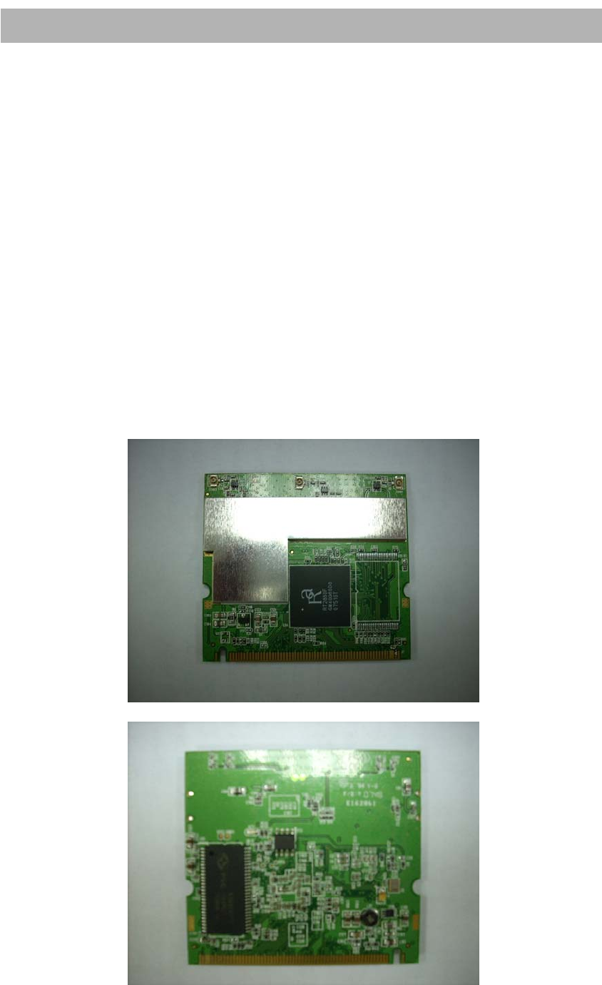
1. Introduction
z Scope
This document describes the IN-7858Mn 802.11b/g/n INIC card hardware
and software specifications.
z Product Features
• Comply with 802.11n draft and 802.11b/g standards.
• High data transfer rate - up to 300Mbps.
• Supports farther coverage, less dead spaces and higher throughput with
MIMO technology.
• Supports 11n Router, 11n ADSL Router, 11n IAD Router, etc. applications.
• Supports WPS (WiFi Protected Setup) interface.
• Supports Linux kernel 2.4/2.6.
• Support Mini-PCI/RGMII/MII interface.

7
2. Product Specification
Product 802.11b/g/n Wireless LAN INIC Card
Model Name: IN-7858MN
Standard IEEE 802.11 b/g and IEEE 802.11n Draft 2.0
Interface Type Mini-PCI/RGMII/MII
Frequency Band 2.4000~2.4835GHz (Industrial Scientific Medical Band)
Modulation OFDM with BPSK, QPSK, 16QAM, 64QAM (11n)
OFDM with BPSK, QPSK, 16QAM, 64QAM (11g)
BPSK, QPSK, CCK (11b)
Data Rate 11n (20MHz): MCS0-15, 32 with Half Guard Interval
Support (up to 144Mbps)
11n (40MHz): MCS0-15, 32 with Half Guard Interval
Support (up to 300Mbps)
11g: 54/48/36/24/18/12/9/6
11b: 11/5.5/2/1Mbps
auto fallback
Antenna I-PEX Connector x 3
OS Linux Kernel 2.4/2.6
Transmit Power 2.4GHz
-11b:17~18dBm
-11g:14~15dBm
-11n:13~15dBm
Receive Sensitivity 2.4GHz
-300Mbps OFDM, 10% PER, -65dBm
-54Mbps OFDM, 10% PER, -74.5dBm
-11Mbps CCK, 8% PER, -89dBm
Dimension 59.75(W) x 54.73(D) x 1.0(H)mm
Temperature 32~122°F (0~50°C)
Humidity Max.95% (NonCondensing)
8
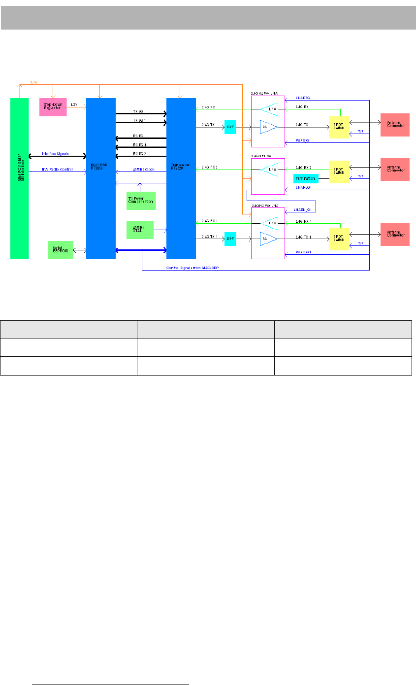
3. Hardware Architecture
z Block Diagram
z Main Chipset Information
Item Model Number Vendor
MAC/BBP/CPU RT2880 Ralink
11b/g/n Transceiver RT2820 Ralink
z Main Chipset Specification
MAC/Baseband Processor
The RT2880 SOC combines Ralink’s 802.11n draft compliant 2T3R MAC/BBP,
a high performance 266-MHz MIPS4KEc CPU core, a Gigabit Ethernet MAC
and a PCI host/device, to enable a multitude of high performance,
cost-effective 802.11n applications. The RT2880 has two RF companion
chips, the RT2820 for 2.4G-band operation and the RT2850 for dual band
2.4G or 5G operation. In addition to the traditional AP/router
application, the chipset can be implemented as an WLAN “intelligent”
NIC, drastically reducing the load on the host SOC, such as DSL/Cable
or Multimedia Applications processors. Users can treat the WLAN iNIC
as a simple Ethernet device for easy porting and guaranteed 802.11n WLAN
performance without the need to upgrade to an expensive host SOC.
RT2880 MAC/BBP/CPU Features
9
• 802.11n MAC/BBP Interface
¾ 2T3R 802.11n MAC/BBP
¾ 300Mbps PHY data rate
¾ 1x1/1x2/1x3/2x1/2x2/2x3 modes
¾ 20Mhz/40Mhz channel width
¾ Legacy and high throughout modes
¾ Reverse Data Grant (RDG) support
¾ Compressed Block ACK
¾ Dual-band: 2.4Ghz or 5Ghz
¾ Up to 256 clients
¾ Multiple BSSID (up to 8)
¾ WEP64/128, WPA, WPA2 engines
¾ QOS - WMM, WMM Power Save Hardware frame aggregation
¾ Cisco CCX Support
¾ International Regulation - 802.11d + h
• MIPS4KEc Core
¾ 266 MHz
¾ 16K I Cache, 16K D Cache
• Gigabit Ethernet MAC interface
¾ 10/100/1000Mbps auto detection
¾ Support RGMII/MII interface
¾ Scatter-Gather DMA
¾ Interrupt mitigation
¾ IEEE 802.3x Flow control
¾ Full/Half duplex
¾ High/Low priority queues
• 33/66Mhz PCI Host Controller
¾ Embedded PCI Arbiter
¾ Supports 2 PCI devices
¾ PCI v2.2 Compliant
• PCI Device interface (WLAN iNIC)
¾ 33/66Mhz x 32-bit DMA master
¾ Scatter-Gather DMA
¾ Interrupt Mitigation
¾ Simple Ethernet-like driver
¾ Ensures wireless LAN peak throughput
¾ High/Low priority queues
• Peripherals

10
¾ UART x2
¾ GPIO x24 (shared)
¾ SPI/PCM
¾ I2C
¾ JTAG
¾ MDC/MDIO
• Packaging
¾ 17mm x 17mm BGA-292 Package
¾ I/O : 3.3V/2.5V(RGMII), 3.3/5V PCI I/O
11b/g/n Transceiver
RT2820 is a monolithic SiGe RF IC that integrates multiple half-duplex
direct-conversion radio transceivers designed for IEEE802.11b/g/n WLAN
systems or other wireless LAN applications operating in 2.4GHz ISM bands.
The IC has two concurrent transmit channels and three concurrent receive
channels. The multiple channels are designed to improve robustness and
throughput during wireless operation. Each receive channel achieves low
noise figure, high input sensitivity, high linearity, and high output
power while consuming low DC power. Each receive path features a gain
selectable, low-noise amplifiers (LNA), followed by RF-to-baseband I/Q
demodulators, discrete-step variable-gain amplifiers and integrated
channel-selection filters. The transmit chain includes integrated
reconstruction filters, a baseband-to-RF I/Q modulator, discrete-step
variable-gain amplifiers for power-level control, and pre-drivers for
external power amplifiers. The modulator and demodulator are driven by
internal VCO. The VCO is phase-locked by an internal 3-wire-interface
PLL. The bandwidth of the integrated channel-selection filters and the
reconstruction filters can be programmed to narrow-band (10MHz) and
wide- band (20MHz). Their bandwidth is calibrated by an internal
autonomous calibration circuit. To help IQ mismatch calibration, a
baseband transmit-to-receive loopback feature is provided. A crystal
oscillator using external crystal and three low dropout regulators (LDO)
are also integrated. The RT2820 is housed in a 76-pin 9x9mm2 leadless
QFN package and is well suited for PCMCIA, MiniPCI, PCI, USB boards or
embedded applications. It is designed to work seamlessly with RT2860B
and RT2880 baseband/Mac IC.
RT2820 Transceiver Features
11
• 3 receivers and 2 transmitters
• 2.4-2.48 GHz band
• Low noise figure
• High linearity
• Low power consumption
• Integrated channel-selection filters
• Integrated reconstruction filters
• Power management/standby mode
• Integrated low dropout regulators
• Single supply 3.0 to 3.6V operation
12
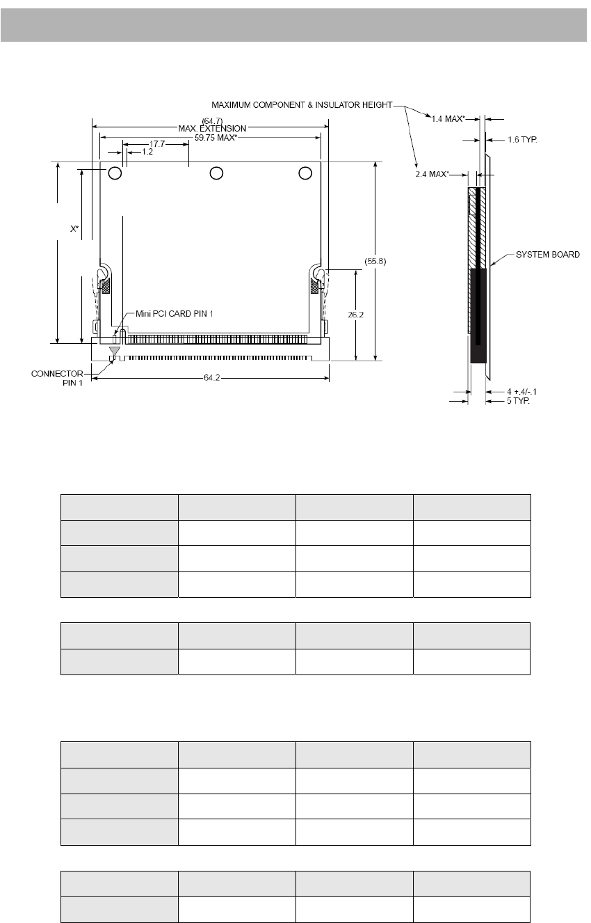
4. Hardware Specification
z Mechanical Form Factor
55
53
z Transmit Power
Channel Channel 1 Channel 7 Channel 13
11b 17.75 17.41 17.51
11g 15.13 15.23 15.35
11n (20MHz)* 15.4/15.2 15/15 15.1/15
Channel Channel 3 Channel 6 Channel 9
11n (40MHz)* 13.6/13.5 13.6/13.4 13.9/13.9
z Receiver Sensitivity
Channel Channel 1 Channel 7 Channel 13
11b -89 -89 -89
11g -74.5 -74.5 -74.5
11n (20MHz) -68 -68 -68
Channel Channel 3 Channel 6 Channel 9
11n (40MHz) -65 -65 -65
13
5. Pin Specification
z Pin Description
Pin Name Pin Name
1 NC 2 NC
3 NC 4 NC
5 NC 6 NC
7 NC 8 Wireless LED
9 AP Mode 10 Reset Default
11 LED ACT 12 LED 2.4G
13 NC 14 LED 5G
15 CHSGND 16 Soft Reset
17 INTB# 18 NC
19 3.3V 20 INTA#
21 NC 22 MA17
23 GND 24 3.3AUX
25 CLK 26 RST#
27 GND 28 3.3V
29 REQ# 30 GNT#
31 3.3V 32 GND
33 AD31 34 NC
35 AD29 36 NC
37 GND 38 AD30
39 AD27 40 3.3V
41 AD25 42 AD28
43 MDC 44 AD26
45 C/BE3# 46 AD24
47 AD23 48 IDSEL

14
Pin Name Pin Name
49 GND 50 GND
51 AD21 52 AD22
53 AD19 54 AD20
55 GND 56 PAR
57 AD17 58 AD18
59 C/BE2# 60 AD16
61 IRDY# 62 GND
63 3.3V 64 FRAME#
65 CLKRUN# 66 TRDY#
67 SERR# 68 STOP#
69 GND 70 3.3V
71 PERR# 72 DEVSEL#
73 C/BE1# 74 GND
75 AD14 76 AD15
77 GND 78 AD13
79 AD12 80 AD11
81 AD10 82 GND
83 GND 84 AD9
85 AD8 86 C/BE0#
87 AD7 88 3.3V
89 3.3V 90 AD6
91 AD5 92 AD4
93 GE_RXDV 94 AD2
95 AD3 96 AD0
97 NC 98 DISABLE_RF_TX
99 AD1 100 WPS
101 GND 102 GND

15
Pin Name Pin Name
103 GE_RXD1 104 MA11
105 GE_RXD2 106 GE_RXD0
107 GE_RXD3 108 GE_RXCLK
109 GE_TXEN 110 GE_TXCLK
111 GE_TXD3 112 GE_TXD0
113 GND 114 GND
115 GE_TXD1 116 GE_TXD2
117 GND 118 GND
119 GND 120 GND
121 MDIO 122 MPCIACT#
123 NC 124 3.3V

16
z RGMII/MII interface
Pin Name I/O Description
22 HOST I MII/PCI Select. 1: RGMII/MII (Pull High) 0: PCI (Pull
Low)
43 MDC O PHY Management Clock
93 GE_RXDV I RGMII/MII RX Data Valid
103 GE_RXD1 I RGMII/MII RX Data bit #1
105 GE_RXD2 I RGMII/MII RX Data bit #2
106 GE_RXD0 I RGMII/MII RX Data bit #0
107 GE_RXD3 I RGMII/MII RX Data bit #3
108 GE_RXCLK I/O RGMII/MII RX Clock
109 GE_TXEN O RGMII/MII TX Data Enable
110 GE_TXCLK I/O RGMII/MII TX Clock
111 GE_TXD3 O RGMII/MII TX Data bit #3
112 GE_TXD0 O RGMII/MII TX Data bit #0
115 GE_TXD1 O RGMII/MII TX Data bit #1
116 GE_TXD2 O RGMII/MII TX Data bit #2
121 MDIO I/O PHY Management Data (RGMII/MII Select. 1: RGMII
(Pull High) 0:MII (Pull Low))