Elettronika S r l TXUD1000A 1000 W ATSC Transmitter User Manual Exciter Manual
Elettronika S.r.l. 1000 W ATSC Transmitter Exciter Manual
Contents
- 1. TXUD1000A User Manual Part 1
- 2. TXUD1000A User Manual Part 2
- 3. Exciter Manual
Exciter Manual

ATSC TV Digital Transmitter
CODE APD043A_APD047A_APD045A TITLE ATSC TV DIGITAL TRANSMITTER REV 1 DATE 29/10/08

SS 96 Km 113
70027 Palo del Colle (Ba) ITALY
Tel. +39 (0)80 626755
Fax +39 (0)80 629262
E-mail: elettronika@elettronika.it
Web site: http://www.elettronika.it
Registration number: IT-17686
Registration number: IT-24436
ATSC Transmitter Family
CODE MODEL
APD043A ATSC UHF TRANSMITTER
APD047A ATSC VHF-III TRANSMITTER
APD045A ATSC VHF-I TRANSMITTER

ATSC Transmitter Family .................................................................................................. 2
Summaries ......................................................................................................................... 3
Warning .............................................................................................................................. 7
Warranty ............................................................................................................................. 8
Introduction ....................................................................................................................... 9
Content of the manual ...................................................................................................... 9
Treatment of electrical shock ......................................................................................... 11
First-aid ......................................................................................................................... 12
Treatment of electrical burns ......................................................................................... 12
Note ............................................................................................................................... 12
RoHS Normative .............................................................................................................. 13
ATSC TV DIGITAL TRANSMITTER .................................................................................. 15
Section 1 - Information ................................................................................................... 17
1.1 Description .............................................................................................................. 18
1.2 Main Features ......................................................................................................... 18
1.3 Technical Characteristics......................................................................................... 19
- Front panel .................................................................................................................. 20
- Rear panel................................................................................................................... 21
- Block Diagram .............................................................................................................22
1.4 Operational Details .................................................................................................. 23
1.4.1 TS Input Management ...................................................................................... 23
- Redundancy management .................................................................................. 23
- Smart switching ...................................................................................................24
- Reed Solomon FEC ............................................................................................ 24
- Bit rate adaptation ...............................................................................................24
- Squelch ............................................................................................................... 24
1.4.2 Synchronization and Clocks ............................................................................. 25
1.4.3 Output Signal ................................................................................................... 25
1.4.4 Non-Linear Precorrection ................................................................................. 26
1.4.5 Linear Precorrection ......................................................................................... 26
1.4.6 Control of the equipment .................................................................................. 26
1.4.7 Test Modes ....................................................................................................... 27
1.4.8 Power Handling ................................................................................................ 27
1.4.9 Alarms and Automation .................................................................................... 28
- Amplifier Voltage .................................................................................................28
- Amplifier Current .................................................................................................28
- Amplifier Temperature ......................................................................................... 28
- Forward and Reflected Power............................................................................. 29
Summaries

- Power supply voltages (-5V, +12V, -12V) ............................................................ 29
- No communication, Temperature and Generic modulator alarm ......................... 29
- External reference alarm ..................................................................................... 29
- ASI/SMPTE inputs alarm ..................................................................................... 29
1.4.10 AGC: Implementation and Details .................................................................. 30
- ATSC TRANSMITTER AGC Cable.......................................................................... 32
1.4.11 Log ................................................................................................................. 33
Section 2 - Installation .................................................................................................... 35
2.1 Operating Environment ........................................................................................... 36
2.2 First Installation ....................................................................................................... 36
2.3 ATSC TRANSMITTER with GPS Clock Source ...................................................... 37
2.4 ATSC TRANSMITTER remote control with Elettronika RCU ................................... 37
2.5 ATSC TRANSMITTER with PC ............................................................................... 38
Section 3 - Operation ...................................................................................................... 39
3.1 Local Control ...........................................................................................................40
3.2 LEDs ....................................................................................................................... 40
3.3 Menu Management ................................................................................................. 40
3.3.1 Title Bar ............................................................................................................ 41
3.3.2 Status Bar ......................................................................................................... 41
3.3.3 Diagram Screen ............................................................................................... 42
3.3.4 Browsing the menus and parameters ............................................................... 42
3.3.5 Composition of a menu .................................................................................... 44
- Submenus ........................................................................................................... 44
- Read/write parameters ........................................................................................ 45
- Read-only parameters ......................................................................................... 45
3.4 Parameters and menu description .......................................................................... 46
3.4.1 Input Menu ....................................................................................................... 46
- Configuration submenu ....................................................................................... 47
- Smart Switching submenu .................................................................................. 48
- VCT submenu ..................................................................................................... 49
- Stream1 Status submenu .................................................................................... 50
- Stream2 Status submenu .................................................................................... 51
- References submenu .......................................................................................... 52
3.4.2 Modulation Menu .............................................................................................. 53
3.4.3 RF Menu...........................................................................................................54
- Frequency submenu ........................................................................................... 55
- Power submenu .................................................................................................. 56
- Amplifier submenu ............................................................................................... 58

- Output submenu.................................................................................................. 59
- Precorrection submenu ....................................................................................... 59
3.4.4 Setup Menu ...................................................................................................... 60
- Control submenu ................................................................................................. 61
- Display submenu................................................................................................. 62
- Clock submenu .................................................................................................. .62
- Power Supply submenu ...................................................................................... 63
- Versions submenu .............................................................................................. 63
3.5 Log Screen ..............................................................................................................64
3.6 Alarm Screen ........................................................................................................... 64
3.7 Firmware Upgrade................................................................................................... 64
ATSC TRANSMITTER Menu Map ................................................................................. 66
Section 4 - Diagram ......................................................................................................... 67
- APD043A ATSC TRANSMITTER Cable Diagram ....................................................... 68
- APD047A ATSC TRANSMITTER Cable Diagram ....................................................... 69
- APD045A ATSC TRANSMITTER Cable Diagram ....................................................... 70
- APD043A_APD047A_APD045A ATSC TRANSMITTER Component list .................... 71
- SCH0135A Control Board and Display ....................................................................... 73
- Description .............................................................................................................. 73
- Dip-switch............................................................................................................ 73
- Technical Characteristics ........................................................................................ 73
- SCH0135A Top layer Component layout..................................................................... 74
- SCH0135A Bottom layer Component layout ............................................................... 75
- SCH0135A Component list ......................................................................................... 76
- A1592 ATSC UHF Modulator Module .......................................................................... 78
- Description .............................................................................................................. 78
- Main Features .........................................................................................................78
- Connectors .............................................................................................................. 78
- A1703 ATSC VHF-I/III Modulator Module .................................................................... 79
- Description .............................................................................................................. 79
- Main Features .........................................................................................................79
- Connectors .............................................................................................................. 79
- MTF0116A 5W UHF RMS Amplifier Module ................................................................ 80
- Description .............................................................................................................. 80
- Technical Characteristics ........................................................................................ 80
- MTF0116A Component list ...................................................................................... 80
- MTF0116A Component layout ................................................................................. 81
- SCH0417A Component layout ................................................................................ 82

- SCH0417A Component list ..................................................................................... 83
- MTF0118A 5W VHF-I/III RMS Amplifier Module .......................................................... 84
- Description .............................................................................................................. 84
- Technical Characteristics ........................................................................................ 84
- MTF0118A Component list ...................................................................................... 84
- MTF0118A Component layout ................................................................................. 85
- SCH0436A Component layout ................................................................................ 86
- SCH0436A Component list ..................................................................................... 87
- MTF0125A 5W VHF-I RMS Amplifier Module ............................................................. 89
- Description .............................................................................................................. 89
- Technical Characteristics ........................................................................................ 89
- MTF0125A Component list ...................................................................................... 89
- MTF0125A Component layout ................................................................................ 90
- SCH0320A Component layout ................................................................................ 91
- SCH0320A Component list ..................................................................................... 92
- SCH0388B Power Supply Interface Board ................................................................. 93
- SCH0388B Power Supply Interface Board Component layout ............................... 93
- SCH0388B Component list ..................................................................................... 94
- E0064 SP-320-27/48 Switching power supply ............................................................ 95
- Main Features .........................................................................................................95
- Mechanical Specifications ....................................................................................... 95
- Technical Characteristics ........................................................................................ 96

7
WARNING
The apparatus described in this manual has been designed and manufactured with devices to safe-
guard the users. In any case it is recommended that during any operation of installation, maintenance,
miscellaneous interventions and calibrations requiring the apparatus to be switched on,
THE USER TAKES ALL THE
PRECAUTIONS AGAINST INCIDENTS
It is required to use the proper clothes and protection gloves in order to prevent damages from inci-
dental contacts with high-voltage parts.
The manufacturer declines every responsibility in case the recommendations above are not followed.
IMPORTANT
The component lists attached to the relevant electrical diagrams indicate for each item the reference,
the description and the type normally used.
The Elettronika S.r.l. though reserves the right to use or supply as spare parts components with
equivalent characteristics but of a different type, assuring anyway the optimal work of the apparatus
in accordance with the specifications.
The enclosed monographs are solely owned by Elettronika S.r.l.
The use of anything enclosed in this technical manual without explicit authorization given by Elettronika
S.r.l. will be prosecuted by the law.
The data and technical characteristics of the apparatus described in this manual are not compelling for
the manufacturer.
The Elettronika S.r.l. reserves the right to make, without previous notice, modifications or updates in
order to improve the quality of the product.
The general conditions of supply and sale are described in the contracts.
The delivery time are in accordance with the products and quantities ordered.

8
Summary of warranty
We, ELETTRONIKA S.r.l., SS096 Km 113 Z.I. PALO DEL COLLE (BA) ITALY, warrant to the ORIGINAL PURCHASER of a NEW product, for a
period of one (1) year from the date of purchase by the original purchaser (the “warranty period”) that the new ELETTRONIKA product is free of defects
in materials and workmanship and will meet or exceed all advertised specifications for such a product. This warranty does not extend to any subsequent
purchaser or user, and automatically terminates upon sale or other disposition of our product.
Items excluded from this ELETTRONIKA warranty
We are not responsible for product failure caused by misuse, accident, or neglect. This warranty does not extend to any product on which the serial
number has been defaced, altered, or removed. It does not cover damage to loads or any other products or accessories resulting from ELETTRONIKA
product failure. It does not cover defects or damage caused by use of unauthorized modificstions, accessories, parts, or service.
What we will do
We will remedy any defect, in material or workmanship (except as excluded), in our sole discretion, by repair, replacement, or refund. If a refund is
elected, then you must make the defective or malfunctioning component available to us free and clear of all liens or other encumbrances. The refund will
be equal to the actual purchase price, not including interest, insurance, closing costs, and other finance charges less a reasonable depreciation on the
product from the date of original purchase. Warranty work can only be performed at our authorized service centers or at our factory. Expenses in
remedying the defect will be borne by ELETTRONIKA, including one-way surface freight shipping costs within the United States. (Purchaser must bear
the expense of shipping the product between any foreign country and the port of entry in the United States and all taxes, duties, and other custom’s fee(s)
for such foreign shipments).
How to obtain warranty service
You must notify us of your need for warranty service not later than ninety (90) days after the expiration of the warranty period. We will give you an
authorization to return the product for service. All components must be shipped in a factory pack or equivalent which, if needed, may
Desclaimer of consequential and incidental damages
You are not entitled to recover from us any consequential or incidental damages resulting from any defect in our product. This includes any damage
to another product or products resulting from such a defect.
Warranty alterations
No person has the authority to enlarge, or modify this warranty. The warranty is not extended by the lenght of time for which you are deprived of
the use of the product. Repairs and replacement parts are provided under the terms of this warranty shall carry only the unexpired portion of this
warranty.
Design changes
We reserve the right to change the design of any product from time to time without notice and with no obligation to make corresponding changes in
products previously manufactured.
Legal remedies of purchaser
There is no warranty which extends beyond the terms hereof. This written warranty is given in lieu of any oral or implied warranties not contained
herein. We disclaim all implied warranties, including without limitation any warranties of merchantability or fitness for a particular purpose. No action
to enforce this warranty shall be commenced later than ninety (90) days after expiration of the warranty period.
Warranty for electronic tubes
The warranty applied for electronic tubes is the one given by the manufacturer of the tube. In the event that the product shows anomalies within the
deadline of the validity of the warranty given by the manufacturer of the product itself, the buyer will have to return it to the seller with the needed
documents and the written description of the defect. The seller will ship the broken tube to the manufacturer in order to effect the necessary technical
tests to find out the cause of the anomaly. Meanwhile the buyer of the tube who needs to use, and as such to replace immediately the product, will have
to buy a new one and provide to the relevant payment, further to the issuing by the seller of a regular commercial invoice. After the adequate tests made
by the manufacturer, should the result be positive, that is confirm the defect in manufacturing, the seller will issue a regular credit note in the name of
the buyer and return the amount paid. Should the result be negative, that is detect a negligence in the installation or use by the buyer, he will have no
right against the seller.
Warranty

9
INTRODUCTION
The apparatus described in this manual is the latest of this series, offering high performances, remark-
able reliability and a wide range of characteristics, it all at a competitive cost.
Its is easy to install and use. It only takes to follow the installation procedure as shown in this manual:
after having removed all from the package, you only have to follow step by step the description in the
various sections.
Before starting to use the apparatus, remember to:
read carefully the general safety information contained in this section;
follow the instructions for the installation and set up of the apparatus;
read all the remaining sections of this manual in order to know well the apparatus and learn
how to obtain the best of its characteristics.
CONTENTS OF THE MANUAL
The chapter composing this manual contain all the information concerning the use of the apparatus.
For more information refer to ELETTRONIKA S.r.l.
This manual is made up of different chapters, each made up of various sections.

10
WARNING!
The currents and voltages in this equipment are dangerous!
Personnel must at all times observe safety regulation!
This manual is intended as a general guide for trained and qualified personnel who are aware of the
dangers inherent in handling potentially hazaedous electrical and electronic circuits.
It is not intended to contain a complete statement of all safety precautions which should be observed by
personnel in using this or other electronic equipment.
The installation, operation, maintenance and service of this equipment involves risks both to personnel
and equipment, and must be performed only by qualified personnel exercising due care.
Elettronika S.r.l. shall not be responsible for injury or damage resulting from improper procedures or
from the use of improperly trained or inexperienced personnel performing such tasks.
During installation and operation of this equipment, local building codes and fire protection standards
must be observed.
WARNING!
Always disconnect power before opening covers,
doors, enclosures, gates, panels or shields.
Always use grounding sticks and short out high
voltage points before servicing. Never make
internal adjustments, perform maintenance or
service when alone or when fatigued.
Do not remove, short-circuit or tamper with interlock switches on access covers, doors, enclosures,
gates, panels or shields.
Keep away from live circuits, know your equipment and don’t take chances.
WARNING!
In case of emergency ensure that power has been disconnected.

11
A - AIRWAY
If unconscious, open airway lift up neck, push
forehead back, clear out mouth if necessary,
observe for breathing.
Treatment of electrical shock
1) If victim is not responsive follow the A, B, C’s of basic life support.
PLACE VICTIM FLAT ON HIS BACK ON A HARD SURFACE
B - BREATHING
If not breathing, begin artificial breathing. Tilt
head, pinch nostrils, make airttght seal, 4 quick
full breaths. Remember mouth to mouth resuscita-
tion must be commenced as soon as possible.
C - CIRCULATION
Check carotid pulse. If pulse
absent, begin artificial circulation.
Approx. 80sec.: 1 rescuer, 15 compressions, 2 quick breaths.
Approx. 60sec.: 2 rescuers, 5 compressions, 1 breath.
NOTE: DO NOT INTERRUPT RHYTHM
OF COMPRESSIONS WHEN SECOND PERSON
IS GIVING BREATH.
Call for medical assistance as soon as possible.

12
2) If victim is responsive:
- keep them warm;
- keep them as quiet as possible;
- loosen their clothing (a reclining position is recommended).
FIRST-AID
Personnel engaged in the installation, operation, maintenance or servicing of this equipment are urged
to become familiar with first-aid theory and practices. The following information is not intended to be
a complete first-aid procedure, it is brief and is only to be used as a reference. It is the duty of all
personnel using the equipment to be prepared to give adequate Emergency First Aid and thereby pre-
vent avoidable loss of life.
TREATMENT OF ELECTRICAL BURNS
1) Extensive burned and broken skin.
- Cover area with clean sheet or cloth (cleansed available cloth article);
- do not break blisters, remove tissure, remove adhered particles of clothing, or apply any salve or
ointment;
- treat victim for shock as required;
- arrange transportation to a hospital as quickly as possible;
- if arms or legs are effected keep them elevated.
NOTE
If medical help will not be available within an hour and the victim is conscious and not vomiting, give
him a weak solution of salt and soda: 1 level teaspoonful of salt and 1/2 level teaspoonful of baking
soda to each quart of water (neither hot or cold).
Allow victim to sip slowly about 4 ounces (half a glass) over a period of 15 minutes.
Discontinue fluid if vomiting occurs (do not give alcohol).
2) Less severe burns - (1st & 2nd degree).
- Apply cool (not ice cold) compresses using the cleansed available cloth article;
- do not break blisters, remove tissue, remove adhered particles of clothing, or apply salve or ointment;
- apply clean dry dressing if necessary;
- treat victim for shock as required;
- arrange transportation to a hospital as qickly as possible;
- if arms or legs are affected keep them elevated.

13
Further to the directives issued by the European Community, 2002/95/CE, 2002/95/CE and 2003/108/
CE, and to the Italian Decree of Law n° 151 dated 25 July 2005, this is to inform the customers of Elettronika
S.r.l. living within the boundaries of the European Community about the following obligations:
1) It is forbidden to trash RAEE products (which includes all broadcasting products which are not expressly
labelled as lead-free) along with normal wastes;
2) Such devices must be brought to proper centres able to perform the adequate processing in order to
recycle their parts where possible and dispose of the raw materials contained therein;
3) For equipment purchased from Elettronika after the 13th of August 2005, the gathering, transport, processing,
recycle and disposal operations are responsibility of Elettronika who will bear all related expenses;
4) For equipment purchased from Elettronika before the 13th of August 2005 , the gathering, transport,
processing, recycle and disposal operations are responsibility of Elettronika, who will bear all related expenses,
only if you are purchasing from us new equipment in substitution of the disposed one;
5) Electric and electronic devices contains lead in soldering, cables, etc. This substance pollutes the environment
and may be accumulated in the organism of plants and mammals. It is dangerous for humans because it may
affect blood, bone marrow, peripheral and central nervous system and kidneys, causing anaemia,
encephalopathies (e.g., convulsions), peripheral neuropathies, cramps of the abdomen and kidney damages.
Besides it affects human reproduction and growth.
These devices also contain mercury. From the environmental point of view, this substance is highly toxic for
aquatic life, and can be accumulated in the organism of fish.
Long-term damages to humans can affect the central nervous system and the kidneys, producing irritability,
emotional instability, tremors, damages to the mind and the memory, language disorders. It may also irritate
and whiten the gums, and its effects may be cumulative. Based on tests on animals, it may affect the human
reproduction or growth.
There is also chrome, which may result in irritation of the eyes and respiration system.
Cadmium is also present. In humans it may damage lungs, due to repeated or prolonged contact with its dust,
and kidneys. It may cause cancer.
6) The symbol below marks the devices which cannot be disposed of along with normal wastes, as stated in
1) and 2) above.
7) The payment of fees is foreseen for the non-allowed disposal of such devices.
Communication N°1 -2002/95/CE - RoHS Directive

14
This page is intentionally blank
15
DIGITAL TV
ATSC TRANSMITTER
User’s manual

16
This page is intentionally blank

17
Section 1 - Information
Contents:
1.1 Description
1.2 Main features
1.3 Technical characteristics
Front panel
Rear panel
Block Diagram
1.4 Operational details

18
ATSC TRANSMITTER
1.1 DESCRIPTION
The ATSC TRANSMITTER is an 8-VSB ATSC professional exciter, designed for the most demanding
digital TV broadcasting applications. It integrates a modulator module with up-to-date FPGA technology and
advanced digital signal processing algorithms in order to generate an absolutely accurate output 8-VSB signal,
with exceptionally optimized modulation and the output filtering techniques.
Very high linearity performances are possible thanks to very careful RF design over the entire VHF and UHF
bands and with an optimal digital precorrection engine working simultaneously in the time and frequency
domains. A high degree of reliability is guaranteed, moreover, by the use of oversized cooling devices and by
control circuits operated by modern microprocessor technologies.
The ATSC TRANSMITTER can be used as a stand-alone 5W RMS transmitter or as a driver stage for
amplifiers of greater power. The excellent spectral purity of the conversion oscillator lets the ATSC
TRANSMITTER radiate an 8-VSB signal with an excellent MER value.
The ATSC TRANSMITTER is equipped with a powerful ASI/SMPTE inputs management block which
allows to manage the Transport Stream (TS) inputs in a fully redundant configuration, thus significantly improving
the reliability of the whole broadcasting system in every operating condition.
The ATSC TRANSMITTER is totally compliant to the A/53, A/54 and A/64 ATSC recommendations with
6MHz output channel bandwidth, in VHF and UHF bands.
1.2 MAIN FEATURES
- Compact and cost competitive;
- Top-quality air cooling system;
- Agile output frequency step 1Hz over VHF and UHF bands;
- Complies and exceeds the ATSC recommendations;
- Multi-platform remote control;
- User-friendly Graphical User Interface;
- Very high power efficiency thanks to accurate digital precorrection;
- Easy frequency synchronization.

19
1.3 TECHNICAL CHARACTERISTICS
SIGNAL PROCESSING SECTION
Reference Standard ........................................................................................................................... ATSC A/53, A/54, A/64
ATSC Mode ....................................................................................................................................... 8-VSB 2/3 Trellis Code
Constellation ................................................................................................................................................................ 8-VSB
Code Rate .......................................................................................................................................................................... 2/3
Network Support ........................................................................................................................................................... MFN
Bandwidth .................................................................................................................................................................... 6MHz
Digital Pre-Correction ......................................................................................................................... Linear and Non-Linear
Automatic PCR Restamping ......................................................................................... User enabled with Bitrate adaptation
Test Modes ......................................................................................................... 23-bit PRBS Generator, Single-tone output
CLOCKS AND SYNCHRONIZATION SECTION
Internal Reference ....................................................................................................................................... VCTCXO 10MHz
Internal Reference Stability .......................................................................................................................... < 1ppm (0-50°C)
Internal Reference Aging ................................................................................................................................. < ±1ppm/year
Internal Reference Tuning .......................................................................................................................................... ±5ppm
10MHz Output Reference ..................................................................................................................................... 0dBm ±3dB
External Frequency Reference ......................................................................................................................... 10MHz ±5ppm
Ext. Frequency Reference Interface ........................................................................................ BNC, 50Ω, -15dBm to +15dBm
INPUT SECTION
TS Input ............................................................................................. 2 DVB-ASI + 2 SMPTE-310M inputs fully redundant
Input TS Format ....................................................................... SPTS/MPTS, Burst Mode - Continuous Mode (ASI inputs)
MPEG-2 Packet Length .......................................................................................... 188/204 bytes (ASI), 188 bytes (SMPTE)
Input Data Rate ......................................................................................... 19.392658Mbit/s (SMPTE), up to 60Mbit/s (ASI)
VCT Update .................................................................................Major Channel Number and/or Frequency (user enabled)
OUTPUT SECTION
RF Output Frequency ................................................ VHF band (57-240MHz) step 1Hz, UHF band (470-860MHz) step 1Hz
Output Level ........................................................................................................................................................... 5W RMS
Output Interface ................................................................................................................................. N type connector, 50Ω
Spectrum Polarity ........................................................................................................................ Non-inverted and Inverted
Harmonics and Spurious .......................................................................................................................................... < -50dBc
Pilot Carrier phase noise .................................................................................................................... < -106dBc/Hz @20kHz
EVM ................................................................................................................................................ < 2.5% without equalizer
Inband SNR ..................................................................................................................................... > 32dB without equalizer
Shoulders .................................................................................................................................................................... > 50dB
Inband Ripple ............................................................................................................................................................. < ±5dB
GENERAL
Physical ..................................................................................................................................................... Case 19”-2U, 12kg
Remote Control Port .......................................................................................................................................... RS232/RS485
Remote Control Options .......................................................................... PSTN, GSM, Ethernet, SNMP (with external unit)
Front Panel User Interface ...................................................................................... LCD Display + Rotating knob + 3 LEDs
Power Supply Voltage ........................................................................................................................... 90 - 240VAC 50/60Hz
Power Consumption .............................................................................................................................................. 150VA max
Operating Temperature .............................................................................................................................................. 0 - 50°C
Specifications and characteristics are subject to change without notice
20
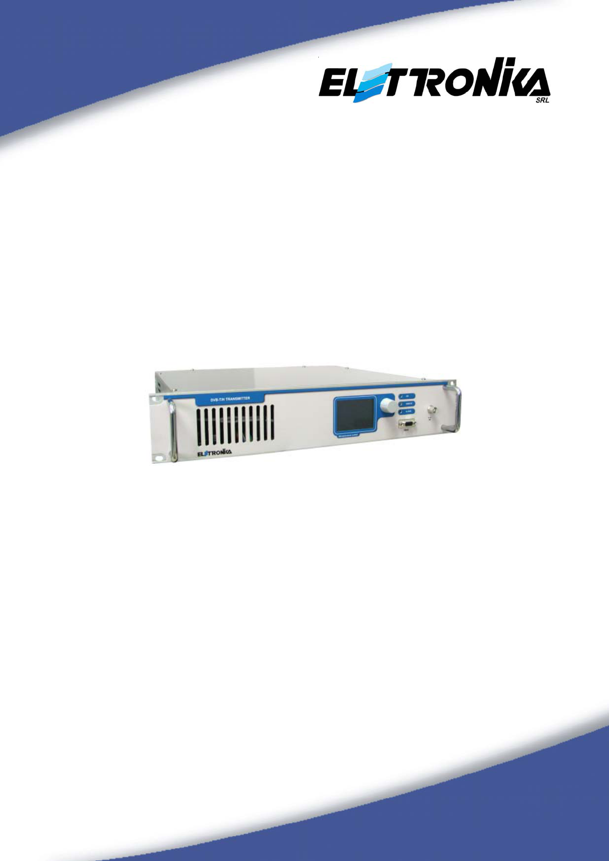
Front panel
1
3
4
5
RS232 for Serial pin-to-pin connection
to PC with ERCos software
and for firmware upgrade
Pin 2: TX
Pin 3: RX
Pin 5: GND
2
DESCRIPTION
1 Graphical LCD
2 Rotating Knob
3 Status LEDs
4 RS232 Socket
5 RF Monitor Connector
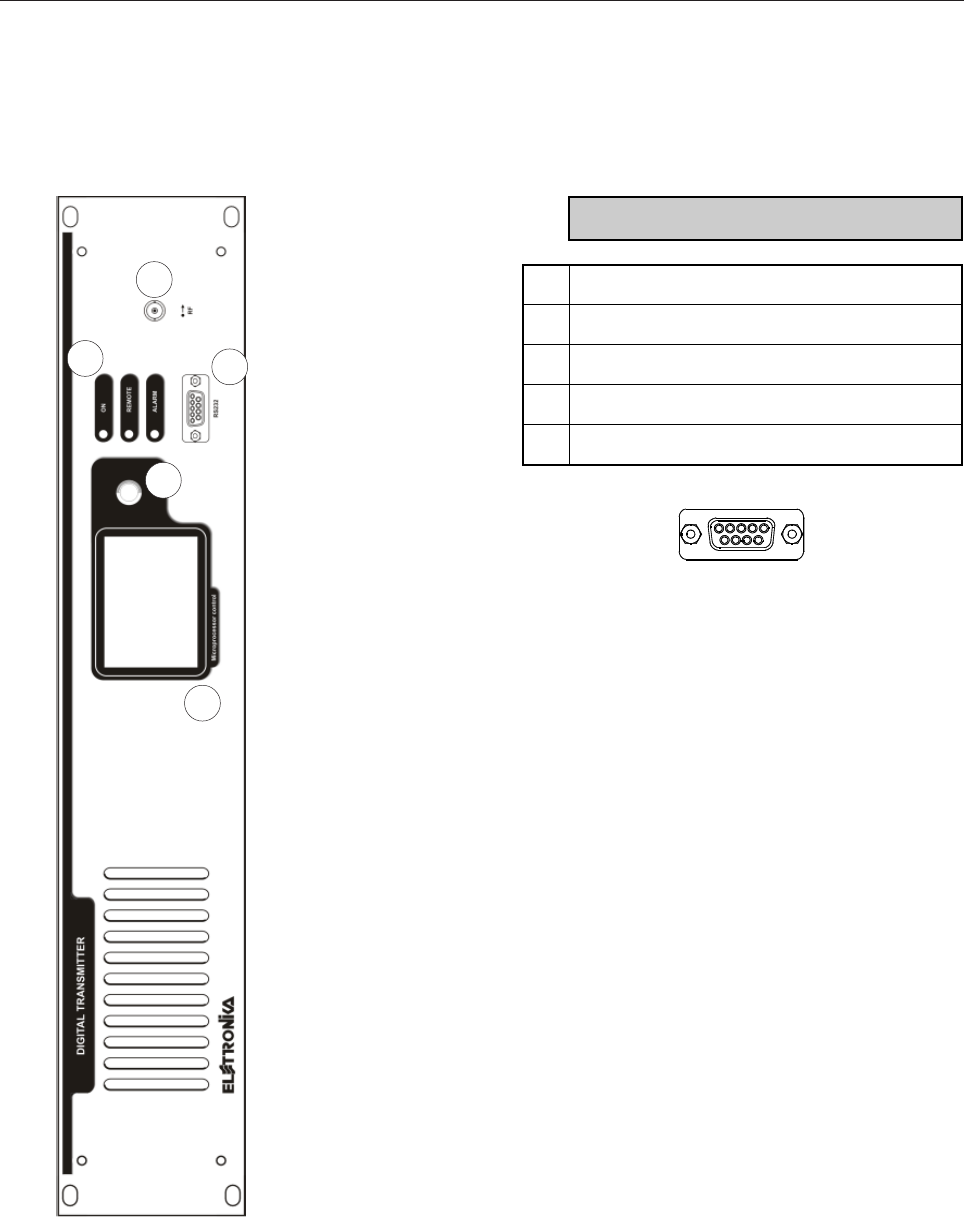
21
LINE SOCKET
RS485
TELEMEASURES
10MHz
IN
RF OUT
10MHz
OUT
SMPTE1
ASI2
ASI1
SMPTE2
Rear panel
1
2
RS485
for Serial pin-to-pin connection
to RCU for remote control
Pin 2: RX- Pin 6: +5V
Pin 3: RX+ Pin 7: TX-
Pin 4: +5V Pin 8: TX+
Pin 5: GND
Wired Telemeasures connector
Pin 1: FWD power (Analog out)
Pin 2: REF power (Analog out)
Pin 3: Temperature (Analog out)
Pin 4: FWD power (Analog in)
Pin 5: GND
Pin 6-7: Alarm or Squelch (user selectable)
Alarm: Open=Normal / Closed=Alarm
Squelch: Open=No Squelch / Closed=Squelch
(Digital out, Free contact relay)
Pin 8: External AGC Alarm (Digital in)
Open=Normal / GND=Alarm
Pin 9: Remote ON/OFF (Digital in)
Open=ON / GND=OFF
8
3
4
5
6
7
DESCRIPTION
1 Main Switch
2 AC Socket with Fuse-Holder (2A)
3 RS485 Socket
4 Telemeasures Connector
5
TS Input Connectors
- ASI1 Input
- ASI2 Input
- SMPTE1 Input
- SMPTE2 Input
6 10MHz OUT Connector
7 10MHz IN Connector
8 RF Output Connector
22
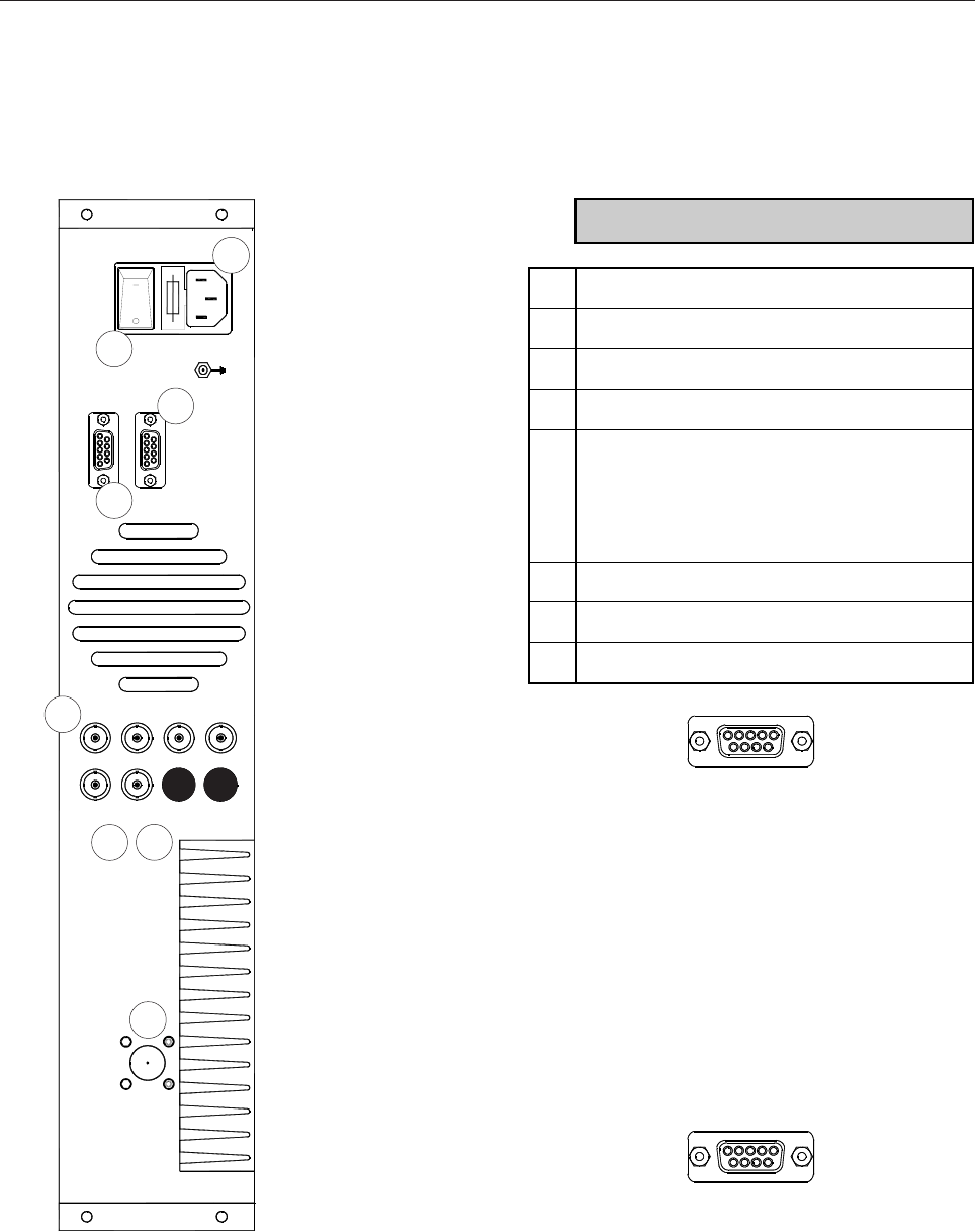
Block diagram
ASI1 INPUT
ASI2 INPUT
SMPTE1 INPUT
SMPTE2 INPUT
REDUNDANCY
CONTROL
8-VSB
MODULATOR CONVERTER
DIGITAL-TO-ANALOG BANDPASS
FILTER
SYNTHESIZER
AGILE LOW-NOISE
FREQUENCY CONVERTER
DUAL-STAGE
AMPLIFIER
OUTPUT RF OUTPUT
POWER SUPPLY SYNCHRONIZATION CONTROL & MONITORING MONITORING OUTPUT
90-250Vac 10MHz IN 10MHz OUT RS232 TELEMEASURESRS485

23
1.4 OPERATIONAL DETAILS
All the sections of the ATSC TRANSMITTER, as showed in the block diagram above, are described in this
chapter in order to give the user a general understanding of the operations of the equipment.
1.4.1 TS INPUT MANAGEMENT
The ATSC TRANSMITTER is equipped with 2 ASI inputs and 2 SMPTE-310M inputs. Each input standard
is available with two inputs in order to enable redundant operation for the transport stream input. You can
decide to operate with SMPTE input or with ASI input depending on your network interfacing needs. In
either case a complete redundancy is guaranteed thanks to a duplicated input.
The ATSC transmission scheme is built over a very stable and accurate data stream clock. The SMPTE-
310M data clock shall have the exact standardized clock frequency. The modulator module takes its
synchronization from this input data stream to be able to recover the same clock frequency. If an external
clock reference is used (10 MHz), the global clock synchronization might be plesiochronous (i.e. not perfect
synchronization between the multiplexer clock and the modulator reference clock). In that case, it is
recommended to enable the "bit rate adaptation" on the ATSC TRANSMITTER.
When this mode of operation is enabled, the input processing module discards or inserts Null Packets in order
to adapt the MPEG-TS input bit rate to the precise bit rate defined by the ATSC recommendation. PCR re-
stamping is then executed accordingly.
The switching is not expected to be seamless. However, in case of feeding the exact data stream on both
inputs (Primary & Secondary), then the ATSC TRANSMITTER performs a seamless switching from one to
the other input. Switching is always performed on a packet basis.
The user may enable or disable the automatic mute when an error on the SMPTE-310M or on the ASI input
is detected (Mute on Input Error feature). The delay for the detection of the lost of SMPTE-310M is 1
second from its occurrence. In case the user disables the automatic mute, null packets are inserted in order to
feed the modulator section with the exact ATSC bit rate.
The user can enable the PRBS test mode (see Test Modes paragraph for more informations) in order to
ignore the real input streams and use a pseudo-random bit sequence. If PRBS test mode is active, the RF
output is not muted even if the “Mute on Input Error” feature is enabled and no valid stream is present at the
input.
- Redundacy management
When set in Automatic Switching mode (default), the input management unit automatically switches to the
other input if no valid MPEG trasport stream is detected on the active input. If the user chooses to operate in
Manual Switching mode, the selected input remains active even if it isn't valid.
The periodic occurrence of the Sync byte in the MPEG-TS packets is used to decide the validity of the
stream.

24
- Smart Switching
The modulator input interface includes an advanced management feature, called Smart Switching, that allows
an automatic switching from the primary to the secondary MPEG-TS input in case of errors on the Transport
Stream packets. The Smart Switching feature can be enabled or disabled.
The Smart Switching is based on a counter and a threshold: erroneous packets counter (Err Counter) and
erroneous packets threshold (Err Threshold). The input processing section of the modulator counts consecutive
erroneous packets and compare them with the Err Threshold: if the Err Counter goes over the Err Threshold,
the switching to the other input takes place. From now on, the modulator compare the Err Counter of the new
input with the Err Threshold.
Errors detected by the modulator that increase Err Counter are the stream synchronization error (TS_sync_loss
and Sync_byte_error as described in ETSI TR 101 290) and RS decoding failure (only for 204-bytes MPEG
packets on ASI inputs).
Together with Smart Switching feature, it's also possible to enable the Auto Switch Back feature in order to
configure a priority input that is active when it is valid. This sub-feature is based on another counter and
another threshold: valid packets counter (Ok Counter) and valid packets threshold (Ok Threshold). When
the Auto Switch Back feature is enabled, the currently active input is assumed as the priority input. After a
Smart Switching to the secondary input (as described above), the priority input is selected again if its Ok
Counter goes over the Ok Threshold.
In this way it's possible to configure a histeresis that avoid false switching with noisy inputs.
The OK Threshold and Err Threshold can be freely changed to finely adjust the switching histeresis (default
values for OK Threshold is 5, for Err Threshold is 80000).
- Reed Solomon FEC
If the ASI incoming inputs (note: only for ASI input mode) include the Reed Solomon codes (204 bytes
packets), the module performs the error correction thanks to the 16 RS bytes.
- Bit rate adaptation
When operating in ASI input mode, the input management unit can perform an automatic bit-rate adaptation,
if required. When this mode of operation is activated, the unit automatically removes and/or inserts null packets
in order to adapt the incoming ASI bit-rate to the exact bit-rate defined by the ATSC recommendation. PCR
restamping is then executed in real time.
- Squelch
The RF output signal can be muted if one of the following conditions occurs:
- a hardware problem is present (for example, the amplifier temperature is too high, the modulator does not
communicate with the controller and so on);

25
- an error in the input signals is present (input TS missing and Mute on input error feature enabled).
In the first condition, the output is muted to protect valuable internal parts of the equipment and/or save
power. In the second condition, the output is muted because the signal is most probably unusable by receivers.
This muting action is known as Squelch.
In a dual drive or 1+1 transmitter, the changeover control unit should discriminate if the output power reduction
is caused by a hardware problem (the changeover takes place) or by an input signal problem (the changeover
is not performed). The user can change the meaning of the digital output in the TLM port choosing "Alarm"
(useful to interface a custom remote control system) or "Squelch" (useful to interface a changeover control
unit).
1.4.2 SYNCHRONIZATION AND CLOCKS
The ATSC TRANSMITTER includes its own clock and synchronization generator. A high stability 10MHz
VCTCXO provides the internal clock reference to the clock system of the digital processing section of the
equipment. An external 10MHz reference may be used if a higher stability is needed, or if there is a need to
lock the modulator processing clock or the output carrier frequency to an external reference (i.e. operation in
frequency offset mode).
In special cases, the 10MHz internal clock may be locked to the system clock embedded into the ASI/
SMPTE input signal. In this case, you can not enable the Bit-Rate Adaptation function and the input bit rate
has to be the exact ATSC bit-rate (19.392658Mbit/s). If the ATSC TRANSMITTER is set up to operate
with either of the two external references (from ASI/SMPTE input or from the external 10MHz reference), it
will automatically switch to the internal reference if the external reference is missing. The switching from the
external 10MHz reference to the 10MHz internal clock is totally seamless. The processing clock of the
numerical section of the ATSC TRANSMITTER is always locked to the internal or to the external 10MHz
reference.
1.4.3 OUTPUT SIGNAL
The ATSC TRANSMITTER output signal is available at the output labelled RF OUT on a 50Ω N-type
female connector. The frequency of the output signal can be set in the VHF and UHF bands, depending on the
model type. The frequency can be set by choosing the standard/channel/offset combination (for example,
UHF standard, channel 45 and offset 0Hz) or by choosing directly the center frequency of the output signal.
An attenuated version of the output signal is available at the RF Monitor terminal located on the front panel of
the equipment. The maximum nominal output level is 5W RMS, the output power level can be controlled in
AGC (Automatic Gain Control) mode or in manual mode and can be adjusted by the rotating knob located
on the front panel. The output signal may be muted either manually by the user or automatically depending on
some given conditions. The mute can be direct (abrupt muting) or progressive (linearly decreasing function).

26
1.4.4 NON-LINEAR PRECORRECTION
Any solid-state or tube power amplifier will produce intermodulation distortion when fed by the ATSC 8-
VSB signal. Non-linear precorrection is used to compensate the effects of these distortions in order to radiate
a signal with the maximum possible MER value.
The ATSC TRANSMITTER is able to perform non-linear precorrection over a 20MHz bandwidth. For this
purpose, two tables (AM-AM and AM-PM) of maximum 16 taps are used by the modulator.
The AM-AM precorrection table defines the AM-AM curve that will be applied to the output spectrum. For
each tap, the abscissa can be defined from -12dB to +12dB by 0.1dB step and the ordinate can be defined
from -6dB to +6dB by 0.05dB step.
The AM-PM precorrection table defines the AM-PM curve that will be applied to the output spectrum. For
each tap, the abscissa can be defined from -12dB to +12dB by 0.1dB step and the ordinate can be defined
from -25 degrees to +25 degrees by 0.2 degrees step.
Up to 10 non-linear precorrection curves (10 AM-AM and 10 AM-PM tables) can be downloaded and
saved into the equipment memory. For each curve a 10-characters name is associated. By using the local or
remote control it is possible to disable the non-linear precorrection at all or activate one of the saved curves.
Besides the 10 customizable curves, a non-customizable "Null" curve is always available: the AM-AM and
AM-PM tables of this curve are filled by zeros.
1.4.5 LINEAR PRE-CORRECTION
Any output cavity filter will produce amplitude and group delay distortion over the DTMB signal generated by
the transmitter. Linear precorrection is used in order to exactly compensate these distortions in order to
generate a signal which is maximally flat both in amplitude and group delay.
The DTMB TRANSMITTER is able to perform amplitude and group delay correction over the full spectrum
of the output signal.
Up to 2 linear precorrection curves can be downloaded and saved into the equipment memory. For each
curve a 10-characters name is associated. By using the local or remote control it is possible to disable the
linear precorrection at all or activate one of the saved curve. Besides the 2 customizable curves, a non-
customizable “Null” curve is always available: the table of this curve is filled by zeroes.
1.4.6 CONTROL OF THE EQUIPMENT
The ATSC TRANSMITTER can be controlled by means of a user-friendly LCD graphical interface with a
single rotating knob for the menu navigation and for the selections or remotely through a RS232, RS485 or
TELEMEASURES port. The functions of the local and remote control are:
- Setting the operating mode of the ATSC TRANSMITTER and the associated parameters. All these parameters
are stored in a local memory, so the previous operating mode is automatically restored each time after a

27
power cycle.
- Monitoring the status of the equipment.
- Recording events and alarms.
- Firmware upgrades.
- Digital Precorrection through RS232 port and dedicated PC software interface.
1.4.7 TEST MODES
Two test modes are available, to be used only for laboratory or field test. The test modes are directly accessible
from the user menus and are:
1) PRBS Sequence: the ASI/SMPTE input signals are ignored and a 23-bit PRBS sequence replaces the
input payload of the MPEG-TS packets. This test allows measurements on the modulated signal without
the need of a valid ASI/SMPTE input signal.
2) Single Tone: the normal 8-VSB output spectrum is switched off and replaced by a sinusoidal output useful
for frequency converters alignment.
Note: If test mode 2) is active, the ATSC TRANSMITTER does not generate a valid ATSC 8-VSB signal.
1.4.8 POWER HANDLING
After the ATSC TRANSMITTER is powered on, it starts radiating a valid ATSC 8-VSB signal within a short
time. The maximum initial power-on delay is about 20s as factory default value. Any modification of this initial
power-on delay is to be done with the support of the Elettronika Customer Service.
If a valid MPEG-TS signal is received over one of the ASI/SMPTE inputs, then the equipment will immediately
generate the signal on the RF output. In absence of a valid MPEG-TS signal the equipment can be set to be
muted or not.
Enabling the muting function is possible by the user menus, as explained in the Menu Management section of
the present manual.
All the working parameters of the ATSC TRANSMITTER are stored into a non-volatile memory in the
modulator section, so that there is no need to restore the parameters after a power off/on cycle.
The power handling is characterized by 3 states: MUTE, POWER UP and POWER ON.
z MUTE (POWER LED off, fan off): the internal amplifier is switched off by inhibiting the RF transistors
gate.
z POWER UP (POWER LED blinking, fan on): the internal amplifier is switched on and the output power,
starting from -3dB to the final level, is slowly increased following a linear ramp law.
z POWER ON (POWER LED on, fan on): the internal amplifier is switched on (normal working operation).

28
Moving from MUTE to POWER ON state (for example, after switching on or when an active alarm disappears)
is performed by moving through a temporary POWER UP state. Instead, moving from POWER ON to
MUTE state (for example, when a serious alarm occurs or the ASI/SMPTE inputs are corrupted or absent)
is immediate.
1.4.9 ALARMS AND AUTOMATION
The ATSC TRANSMITTER is fully protected against any malfunctioning event that could damage the expensive
internal components. The user should clearly understand what happens in presence of alarms and warnings,
in order to face these situations properly and reduce the inactivity time.
In case of any alarm condition, the ALARM LED on the front panel lights up and a bell icon appears in the
status bar of the display. When the alarm condition ceases, the ALARM LED is turned off and the bell icon
starts blinking, in order to show that an anomaly occurred since the last visit to the log. To know the details
about the alarm event (for example the time and date of its occurrence), the log menu can be used. Once the
user enters the log screen, the bell icon disappears. When you note an active alarm (the bell icon is shown and
not blinking and the ALARM LED
is on), go to the ALARM screen to see which alarms are present. For certain dangerous situations, the ATSC
TRANSMITTER immediately switches off the output power, by acting on the RF power transistors gate, in
order to save the internal parts from an unrecoverable damage. When the alarm disappears, the power is
automatically switched on again. Once the output power has been inhibited for 5 times, the ATSC
TRANSMITTER goes into "Lockout" state: the power remains off until the user resets the Lockout condition,
or switches the equipment off for repair. After one hour from the last alarm and without the Lockout condition,
the Lockout counter is automatically cleared. The list of the automatic interventions in case of anomalies can
be found below.
z Amplifier Voltage
An amplifier power supply voltage alarm occurs when the monitored voltage is outside the nominal level
±10% range. The nominal voltage level is a factory setting (usually, 28V). This alarm does not trigger a
powering off of the output signal. If the monitored voltage is near 0V, most probably the fuse located near the
power amplifier stage is burned.
z Amplifier Current
An amplifier power supply current alarm occurs when the monitored current drained by the amplifier is 20%
above the nominal level. The nominal current level is a factory setting. This alarm does not trigger a powering
off of the output signal.
z Amplifier Temperature
The temperature is monitored on the hottest point, located near the power amplifier stage on the cooling heat
sink. If the fans work well, and the ambient temperature is inside the working conditions limits, all of the

29
internal parts should reach safe temperature levels. In some circumstances (for example, when a fan is blocked
or damaged), the temperature may increase too much, and some internal components may break. In order to
avoid this unpleasant situation, a temperature alarm occurs when the temperature is over a maximum threshold
(75°C). This alarm triggers an immediate powering off of the output signal and an increase of the lockout
counter.
The power will be switched on again only when the temperature goes below a second threshold, lower than
the first (70°C).
z Forward and Reflected Powers
A forward or reflected power alarm occurs when the relevant monitored power level is over a threshold
(factory setting). Both alarms trigger an immediate powering off of the output signal and an increase of the
lockout counter.
You can see the levels of the power thresholds in the Amplifier menu (see the Menu Management paragraph).
z Power supply voltages (+5V, +12V, -12V)
Besides the amplifier power supply voltage (+28V), the ATSC TRANSMITTER uses three additional main
voltages: +5V, +12V, -12V. These voltages are continuously monitored by the control system and any variation
above 10% of the nominal value generates an alarm condition. This alarm does not trigger a powering off of
the output signal.
z No communication, Temperature and Generic modulator alarm
The ATSC Modulator module continuously communicates with the control system. If this communication fails,
the control board triggers a “No communication” alarm. This is a serious malfunction that must be solved as
soon as possible. In presence of a no communication alarm, the control system isn’t able to know the working
condition of the modulator (for example, the modulated output signal level), so it inhibits the power amplifier
stage and the output power is muted. uring normal working conditions, the internal temperature of the modulator
could increase above a safe threshold. In this case, the control system triggers a “Modulator over-temperature”
alarm and the output power is muted to let the temperature decrease.
As the modulator is a complex piece of hardware and software, other erroneous and/or dangerous conditions
could happen. In this cases, the control system triggers a generic “Modulator Error” alarm.
z External reference alarm
When external or ASI/SMPTE reference is set, the modulator continuously monitors the presence of such
reference. If it is not able to find a correct signal, it automatically switches to the internal reference. In this
situation, an external reference alarm is triggered. This alarm does not trigger a powering off event. See the
Synchronization and Clocks paragraph for more information.
z ASI/SMPTE inputs alarm
There are several conditions related to input streams that could trigger an alarm, depending on the working
30
conditions. They are:
- MPEG-TS synchronization missing;
- uncorrected input packet (only in 204 RS coded mode with ASI input mode);
- bit rate underflow/overflow (only if bit rate adaptation is performed).
The above conditions trigger an alarm only for the input which is currently used by the ATSC TRANSMITTER.
1.4.10 AGC: IMPLEMENTATION AND DETAILS
The use of external AGC helps the ATSC TRANSMITTER to maintain stable the output power of a high-
power transmitter. With a menu setting (see the Menu Management paragraph) you can choose among
stabilizing the output power of the exciter (external AGC disabled) or stabilizing the output power of a high-
power transmitter (external AGC enabled). In this case a proper cabling between the ATSC TRANSMITTER
and the high-power amplifier stage is necessary. The cable (AGC cable) shall be connected to the TLM port
of the ATSC TRANSMITTER on one side. In the following table the three signals and pins used in the TLM
port are listed. The pinout connection of the cable depends on the specific amplifier used. Refer to your
amplifier user's manual to find the port and pins of the corresponding signal.
PIN I/O DESCRIPTION
4 I Forward Power (0-5V)
5-GND
8 I Alarm (GND=Alarm / Open=Normal)
The AGC goal is to maintain the output power stable. Output power in fact can change due to the increase of
the amplifier temperature. Note that when you change the operating frequency the output power changes due
to the different gain at different frequency, but this change is not stabilized by the AGC algorithm. The transmitter
power to be stabilized is read from TLM port.
To keep the power stable, the AGC changes the power gain of the ATSC TRANSMITTER.
The AGC algorithm is based on the acquisition of the optimal output power level, stored when you confirm the
output power level in the Power menu (see the Menu management paragraph) and the use of 4 thresholds
as below:
____action threshold
________goal threshold
___________optimal power value
________goal threshold
____action threshold

31
The distance of the thresholds from the optimal value is of ±20mV and ±30mV measured as monitor voltage.
The AGC changes the output power to bring the power from the amplifier inside the goal thresholds range.
When this goal is achieved, the AGC stops until the power goes outside the action thresholds range.
The AGC is stopped immediately (output power remains blocked to the value reached at the moment in
which the AGC stops) when one of the following conditions occurs:
z RF output is muted for an alarm condition or user setting;
z the AGC is chosen as external but the amplifier stage triggers an alarm;
z the ATSC TRANSMITTER output power is too low;
z the AGC has corrected the output power too much.
In order to simplify the understanding of the AGC behaviour, the status of the external AGC is written in the
Power menu (Ext AGC Status parameter). The possible statuses of the AGC are listed below.
z Disabled: external AGC is disabled.
z Idle: external AGC is stopped (for example, during the slow increase of the power immediately after
switching on the equipment).
z Low Set: external AGC is stopped because external power reading was too low when the nominal output
power has been chosen.
z Alarm: external AGC is stopped because an alarm signal from the power amplifier stage is active.
z Locked: the transmitter output power has reached the desired level.
z Max/Min: external AGC is stopped because the power correction is too high.
z Pull Up/Down: external AGC is moving the power level up or down.
Warning! When changing from AUTO to MANUAL power control mode, the external AGC will be disabled.
32

33
1.14.11 LOG
The ATSC TRANSMITTER is provided with an internal non-volatile memory used to store up to 200 events
in a log. For each event, the date, time and a description are stored in order to help the user in understanding
the sequence of the events and the cause of each alarm.
The log can be viewed locally on the display (see the LOG screen in the Menu Management paragraph)
or by remote. It is possible to clear the log contents only locally.
The events are organized from the last one: the first event in the log is the last that happened. The second is the
previous event compared to the first, and so on.
When the log is full (i.e., 200 events are stored), the new events will replace the older ones, like in a FIFO
(first in/first out) queue.
The type of events that can be stored in the log are:
z Power supply on from mains voltage
z Mute settings (automatic/manual) changed
z Remote/local control changed
z Lockout
z Amplifier voltage alarm
z Amplifier current alarm
z orward power alarm
z Reflected power alarm
z Temperature alarm
z Power supply voltage (-12V, +12V or +5V) alarm
z Modulator no communication, over temperature, general error alarm
z External reference alarm
z ASI/SMPTE inputs related alarms

34
This page is intentionally blank

35
Section 2 - Installation
Contents:
2.1 Operating environment
2.2 First installation
2.3 ATSC TRANSMITTER with GPS Clock Source
2.4 ATSC TRANSMITTER remote control with Elettronika RCU
2.5 ATSC TRANSMITTER with PC
36
2.1 OPERATING ENVIRONMENT
You can install the apparatus in a standard component rack or on a suitable surface such as a bench or desk.
In any case, the area should be as clean and well-ventilated as possible. Do not locate the transmitter directly
above a hot piece of equipment.
2.2 FIRST INSTALLATION
Correct installation of the equipment is important for maximum performance and reliability. Antenna and earth
connections must be installed with the greatest care. No equipment adjustment is needed, because the unit is
completely adjusted by our technical staff. This is the installation procedure:
1. Connect Antenna cable.
2. Connect AC POWER cord.
3. Connect the ASI/SMPTE Inputs you want to use depending on available auxiliary inputs (see the table in
Input Management paragraph).
4. Move power slowly up till nominal power and check the Reflected Power to be low. If the Reflected
Power increases check the RF Output connections.
LINE SOCKET
RS485
TELEMEASURES
10MHz
IN
RF OUT
10MHz
OUT
SMPTE1
ASI2
ASI1
SMPTE2
AC POWER
To Bandpass Filter
or High Power Amplifier
ASI/SMPTE INPUT
37
2.4 ATSC TRANSMITTER REMOTE CONTROL WITH ELETTRONIKA RCU
In order to connect the ATSC TRANSMITTER to RCU the RS485 connector must be used and RS485
must be chosen in the ATSC TRANSMITTER menu (Setup J Control J Serial).
2.3 ATSC TRANSMITTER WITH GPS CLOCK SOURCE
1. Connect the 10MHz reference only for higher stability or frequency locking purposes
2. The 1PPS signal is not used for ATSC operation, so leave this output not connected.
LINE SOCKET
RS485
TELEMEASURES
10MHz
IN
RF OUT
10MHz
OUT
SMPTE1
ASI2
ASI1
SMPTE2
GPS CLOCK SOURCE
10MHz OUT
LINE SOCKET
RS485
TELEMEASURES
10MHz
IN
RF OUT
10MHz
OUT
SMPTE1
ASI2
ASI1
SMPTE2
REMOTE CONTROL UNIT
PORT n

38
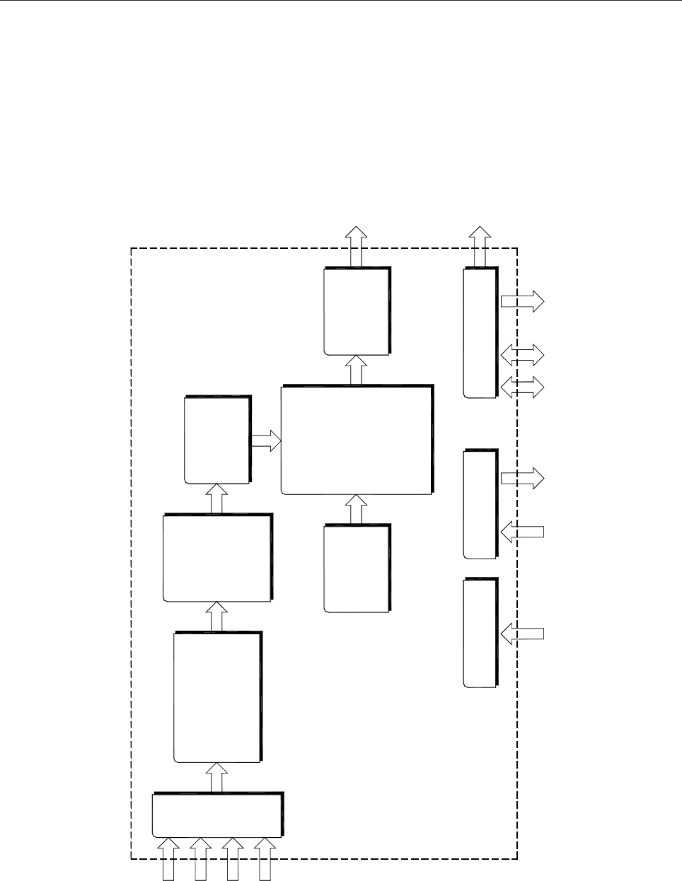
2.5 ATSC TRANSMITTER WITH PC
DVB- T/H TRANSMIT TER
ON
REMOTE
ALARM
Microprocessor control
SERIAL PORT

39
Section 3 - Operation
Contents:
3.1 Local control
3.2 LEDs
3.3 Menu management
3.4 Parameters and menu description
3.5 Log screen
3.6 Alarm screen
3.7 Firmware upgrade
ATSC TRANSMITTER Menu Map
40
3.1 LOCAL CONTROL
A large number of options of the ATSC TRANSMITTER can be easily and intuitively controlled through the
human-to-machine interface on the right side of the front panel. This is composed by a graphic display, a
clickable knob and three LEDs.
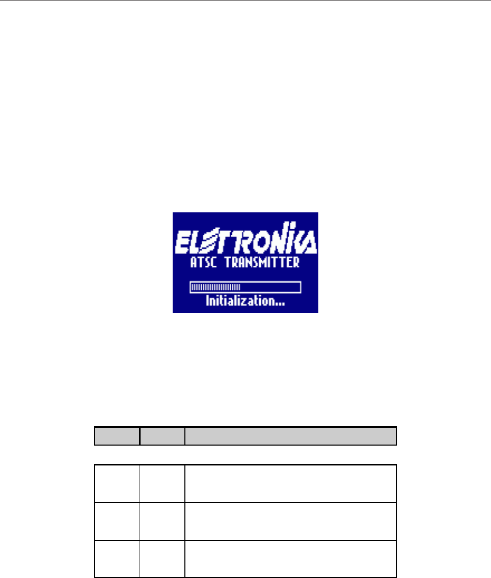
Right after switching on, a screen showing the initialization process appears on the display. During this time the
controller checks the good communication among internal parts of the equipment.
3.2 LEDs
Near the display three status LEDs allow to gather information concerning the general status of the system
without having to look at the display. Their meaning is explained in the table below.
LED COLOUR DESCRIPTION
ON Green
The ON LED is lit when the power is on. It blinks during
the power increase stage. It is off if the output is muted
(see the Power handling paragraph)
REMOTE Yellow The REMOTE LED is lit when the remote control is
enabled
ALARM Red The ALARM LED lights up if some alarm is active
3.3 MENU MANAGEMENT
After the initialization screen, the DIAGRAM screen is shown on the display. It represents a simple diagram
of the machine: ASI/SMPTE inputs, the ATSC modulator, the up-converter and the amplifier. The most
41
important parameters are also shown in this screen. Pressing the knob while in this menu you will be directed
to the RF Power menu for a quick intervention during emergency situations.
3.3.1 TITLE BAR
On the top of the display, the title bar is shown. It is always visible during browsing the various menus and
screens. In the bar two pieces of information are present.
• The name of the screen is displayed on the left (DIAGRAM in the case of the first screen). During settings
change, a confirmation question could appear in this part of the titlebar (see later).
• The actual time is on the right side of the bar. The colon symbol between hours and minutes blinks every
second in order to indicate the progress of time.
3.3.2 STATUS BAR
On the bottom of the display, the status bar is shown. It is always visible while browsing the various menus and
screens. In the bar five pieces of information are present, as described in the following list (the order is from
the left to the right of the bar).
• The bell icon ( ) on the left gives the user some information about alarm conditions that are present or that
occurred in the past. The icon can be absent, present or blinking. The meanings of these conditions are
detailed in the following table.
ICON DESCRIPTION
Absent No alarms are present and no alarms occurred since the last visit to the log
Present At least an alarm is present at the moment
Blinking An alarm occurred since the last visit to the log, but no alarm is present at this moment
• The lock icon ( ) at the right of the bell icon is displayed when the control is password-locked (see later in
this manual for more information about password locking). When the user unlocks it by typing the correct
password, the lock icon disappears.

42
• The Forward Power is shown about at the centre of the status bar. It is indicated in Watt. This is the power
as it is measured by the directional coupler at the very last stage of the power amplifier, just before the
output connector. When the RF is muted, the word MUTE is shown instead of the output power.
• The Reflected Power is shown next to the Forward Power. It is indicated in Watt. This is the power as it is
measured by the directional coupler at the very last stage of the power amplifier, just before the output
connector. When the RF is muted, the word MUTE is shown instead of the Reflected Power.
• The Temperature is shown at the rightmost side of the status bar. It is indicated in Centigrade degrees. This
temperature is measured by a sensor located near the hottest spot of the cooling heat sink of the power
amplifier stage. When a temperature alarm is present (the temperature is over the threshold), the tempera-
ture indication in the status bar blinks.
3.3.3 DIAGRAM SCREEN
The DIAGRAM screen represents a general schematic view of the ATSC TRANSMITTER. The most important
working settings are written using a small-size font. By looking at this diagram, the user can have a general
overview of the equipment status. On the left there is the input section, showing ASI1/ASI2 or SMPTE1/
SMPTE2 depending on the selection made in INPUTJCONFIGURATION menu. In ASI mode, the upper
ASI1 text appears when a valid ASI1 input stream is present. The lower ASI2 text appear when a valid ASI2
input stream is present. These words blink if a bad input stream is detected. The behaviour is identical in
SMPTE mode with a difference only in the strings: SMPTE1 and SMPTE2 instead of ASI1 and ASI2.
The presence of the string indicates only the presence of a corresponding input stream. The actual input
stream used by the modulator is shown by a horizontal line starting from the input name and entering the
modulator. Next to the input section, the modulator block is drawn. On top of the rectangle, the ATSC mode
is written: 8-VSB. The word MODUL blinks if any error associated to the modulator is present.
At the bottom of the modulator rectangle, there is the external reference block. If a valid reference is detected,
the REF rectangle is drawn. If the external reference is actually used by the modulator, a vertical line connect
the REF to the MODUL rectangles. If the user choose to use the external reference, but a good reference
can't be detected, the REF rectangle blinks. Immediately on the right, the up-converter block is drawn. On
top of the rectangle, the RF channel number is written if the frequency is chosen by standard/channel couple.
Nothing appears if the frequency is set manually. The triangle on the right represents the power amplifier and
an hypotetical antenna connected to it. From the output of the power amplifier, two lines start: they indicates
the output power and the reflected power measures shown in the status bar at the bottom of the display.
3.3.4 BROWSING THE MENUS AND PARAMETERS
The user can browse the menus, see the parameters values, change the settings of the machine and make all
the operations simply by using the knob located on the right of the display. The knob can be rotated left or
right and be pushed.
43
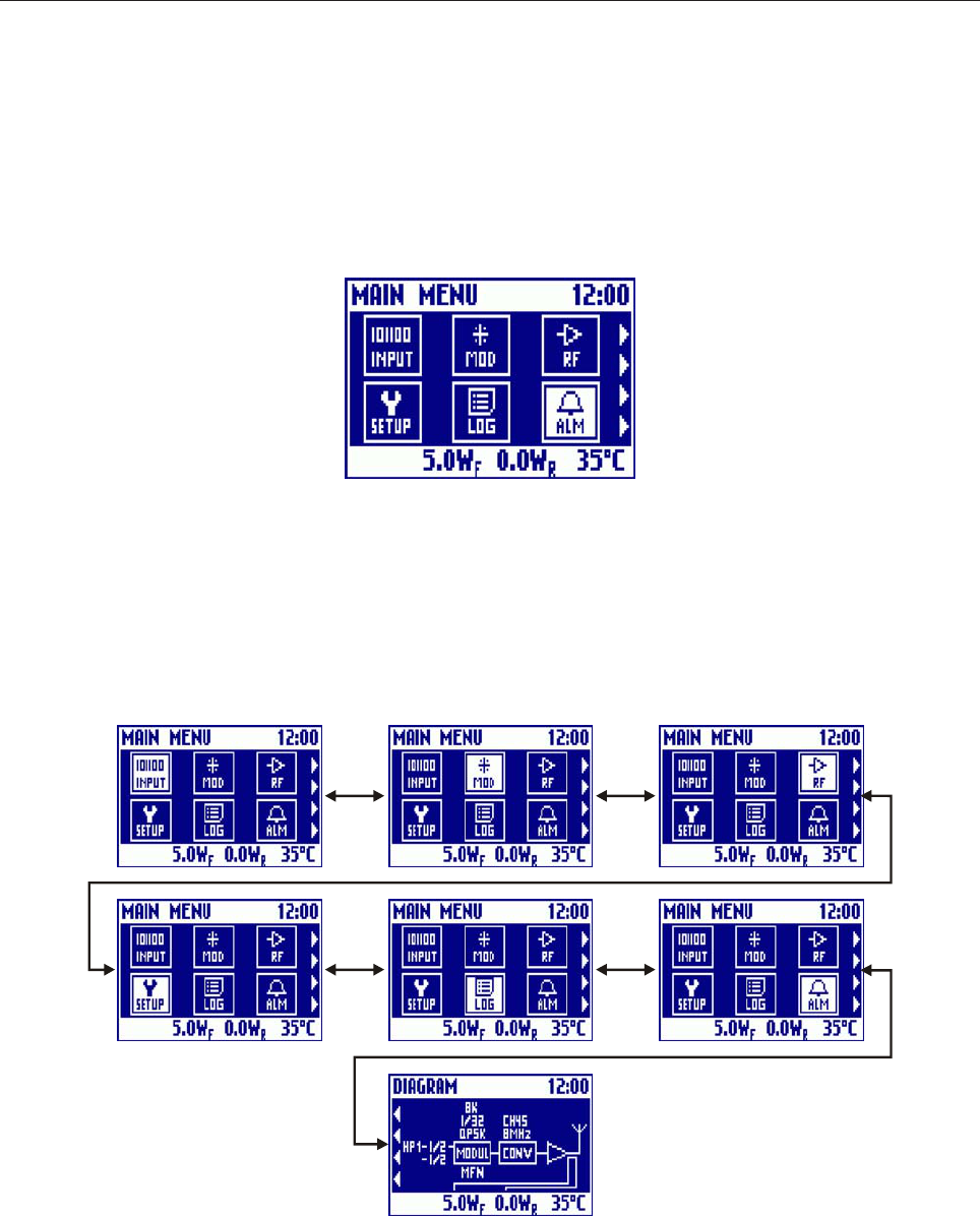
From the first screen (DIAGRAM screen), it is possible to rotate the knob to the left to enter the MAIN
MENU screen.
In this screen six icons (INPUT, MOD, RF, SETUP, LOG, ALM) are shown, arranged in 2 lines of 3 icons.
The selected icon is drawn in reverse colours. By moving from the DIAGRAM screen, the selected icon will
be ALM, as in figure above. It is possible to select the other icons by rotating the knob again to the left. By
rotating the knob to the right, it is possible to select the icons in the opposite order. When the ALM icon is
selected, rotate the knob to the right to go back to the DIAGRAM screen again.
When an icon is selected, click the knob to enter the associated menu. For example, by clicking the knob
when the RF icon is selected, the menu related to the RF signal is shown.

44
The ATSC TRANSMITTER is a complex piece of equipment and its setting could be a difficult task. The
multitude of parameters are arranged in six tree-like menus, starting from the six top-level menu icons. In this
way, it is simpler and more comfortable to find the desired parameter.
3.3.5 COMPOSITION OF A MENU
An example menu (the RF menu) is depicted in the figure below.
The title of the menu (RF in this example) is written at the leftmost side of the titlebar. Every menu is composed
by several items, but only four of them are shown at the same time on the display. The first item is always
“Exit...”. One of the item is selected and is shown in reverse colours. By rotating the knob to the right
(bottom), the selected item is changed and the menu is scrolled down to its last item. By rotating the knob to
the left (up), the menu is scrolled up to its first item. The scrollbar drawn on the left of the items gives an idea
about the selected item position in the menu: the position of the small tab inside the scrollbar changes depending
on the selected item, from the top to the bottom of the outer rectangle representing the bar. There are 3 types
of item in a menu, characterized by a different suffix appended to the item name:
• submenus, with leading dots ( );
• read/write parameters, with a right arrow ( ) suffix;
• read-only parameters, without any suffix.
In case of failure, the value of the failed parameter (read/write or read-only) blinks to show the malfunction,
until the alarm condition disappears. If the “Modulator no communication” alarm is present, the value of
parameters related to the modulator is indicated as “???”.
- Submenus
A submenu item is indicated by the name of the submenu and the leading dots. By clicking on a submenu (e.g.,
by clicking the knob when a submenu item is selected), a new child menu is shown, browsing the tree-like
menu from the top to the bottom. As before, this new (sub) menu is composed by several items that can be
other submenus or parameters.

45
Even if it has leading dots, the “Exit...” item, the first item of all menus, isn’t a real submenu. By clicking on
“Exit...”, it goes back to the parent menu, if any, browsing the tree-menu from the bottom to the top. If the
menu is at the top-level, by choosing “Exit...” the menu icons screen is shown.
- Read/write parameters
The row of a read/write parameter is composed by two parts: the leftmost one contains the name of the
parameter with arrow suffix, the rightmost one contains its value or an “action symbol”.
By clicking on a read/write parameter, the associated value is written in reverse colours, meaning that it is
possible to change it by rotating the knob. Some parameters can be changed continuously in a range (e.g., the
output power level); move the knob to the right (left) to increase (decrease) the value. For other parameters,
the value can be chosen from a short list (e.g., the input selection); move the knob to the right (left) to scroll
down (up) the list. For some other complex parameters, like the frequency or the date, the user can change a
token at a time (a digit of the frequency, a field of the date) by rotating the knob, moving to the next token by
clicking on the knob. After choosing the desired new value, click the knob to finish the change. Usually, until
now, no real change of the parameter took place (there are some exceptions, well described later). It is
necessary to accept the new value by rotating the knob to the right in order to choose the answer “Yes” to the
confirmation question (“Sure?”) that appears at the left of the titlebar. By answering “No” to the confirmation
question, the new value is discarded and the parameter keep the old value.
There are some “special” read/write parameters that represent only an action to make (e.g., Clear Log). Their
value is shown with the symbol. By clicking on this kind of parameter, the symbol is drawn in reverse
colours. Click again and choose “Yes” to the confirmation question in order to perform the associated action
(e.g., clearing the log content). It should be noticed that, if the control is password-locked or the remote
control is enabled, a read/write parameter could become a read-only parameter until the control is unlocked
by typing the correct password or the remote control is disabled.
- Read-only parameters
The row of a read-only parameter is composed by two parts: the leftmost contains the name of the parameter,
the rightmost one contains its value. The user can read this value, but not modify it. In fact, if clicking on a
read-only parameter, nothing happens.

46
3.4 PARAMETERS AND MENUS DESCRIPTION
This paragraph contains a detailed description of all the menus and parameters. Please be sure to read this
section very carefully before changing any setting of the exciter. Check the menu map for a general overview
of the parameters.
The menus and parameters arrangement is subject to change, mostly with the control firmware version.
Your arrangement could be slightly different than the one described in this manual. For any questions,
contact the Elettronika Customer Service.
3.4.1 INPUT MENU
Configuration
Click on this item to enter the Configuration submenu to read and/or modify the ASI/
SMPTE inputs settings.
Stream1 Status
Click on this item to enter the Stream1 Status submenu to read informations (packets
length, Virtual Channel Table informations and so on) of stream 1.
Stream2 Status
Click on this item to enter the Stream2 Status submenu to read informations (packets
length, Virtual Channel Table informations and so on) of stream 2.
References
Click on this item to enter the References submenu to read and/or modify references
settings.
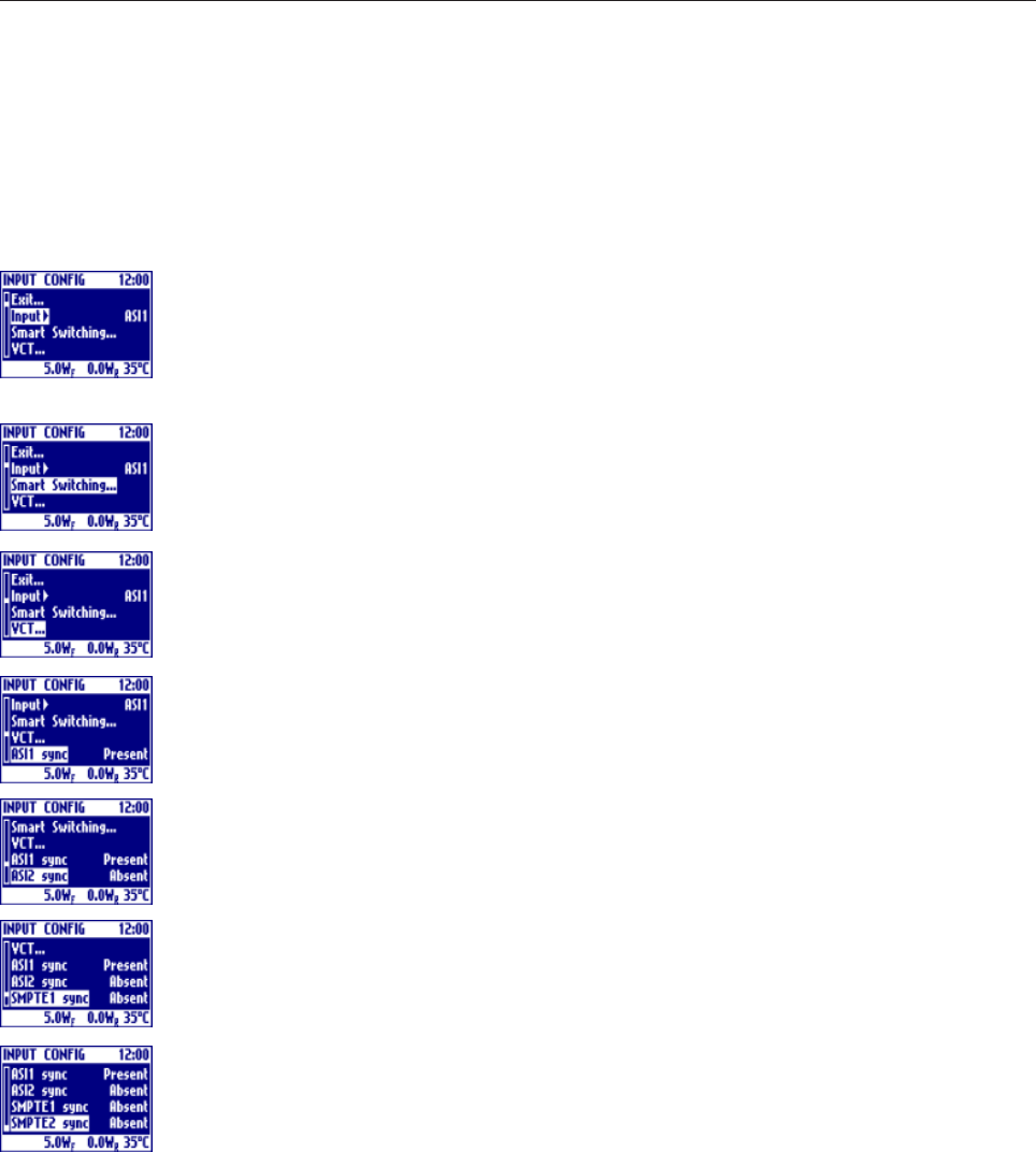
47
- CONFIGURATION submenu
Input (ASI1, ASI2, ASI Auto, SMPTE1, SMPTE2, SMPTE Auto)
This parameter lets to change the input type (ASI or SMPTE) and the stream (1 or 2) used
by the modulator. It's also possible to set the automatic selection mode (see TS INPUT
MANAGEMENT paragraph for more information).
Smart Switching
Click on this item to enter Smart Switching submenu.
VCT
Click on this item to enter VCT submenu.
ASI1 sync (Present, Absent)
If a valid ASI1 input is detected by the modulator, the word Present is written. On the
contrary, if no ASI1 input is detected by the modulator, the word Absent is written.
ASI2 sync (Present, Absent)
If a valid ASI2 input is detected by the modulator, the word Present is written. On the
contrary, if no ASI2 input is detected by the modulator, the word Absent is written.
SMPTE1 sync (Present, Absent)
If a valid SMPTE1 input is detected by the modulator, the word Present is written. On the
contrary, if no SMPTE1 input is detected by the modulator, the word Absent is written.
SMPTE2 sync (Present, Absent)
If a valid SMPTE2 input is detected by the modulator, the word Present is written. On the
contrary, if no SMPTE1 input is detected by the modulator, the word Absent is written.

48
- SMART SWITCHING submenu
See TS INPUT MANAGEMENT paragraph for more information on Smart Switching feature.
Status (Enabled, Disabled)
This parameter lets to enable/disable the Smart Switching.
Switch Back (Enabled, Disabled)
This parameter lets to enable/disable the Auto Switch Back.
Err Thres (00000000-99999999)
This parameter shows the Err Threshold (in packets) used for the Smart Switching.
Click the know on this item to change its value. The reversed digit can be changed by knob
rotation. Click on knob to pass to the next digit up to the last. Clicking on the last digit, the
usual confirmation question appears.
Ok Thres (00000000-99999999)
This parameter shows the Ok Threshold (in packets) used for the Auto Switch Back.
Click the know on this item to change its value. The reversed digit can be changed by knob
rotation. Click on knob to pass to the next digit up to the last. Clicking on the last digit, the
usual confirmation question appears.

49
- VCT submenu
VCT is the acronym for Virtual Channel Table.
MCN Update (Enabled, Disabled)
If this parameter shows Enabled, the Major Channel Number (MCN) field of the VCT is
updated with the value below. If this parameter is disabled, the MCN field is untouched by
the modulator.
Freq. Update (Enabled, Disabled)
If this parameter shows Enabled, the frequency field of the VCT is updated with the value
below. If this parameter is disabled, the MCN field is untouched by the modulator.
MCN (0-99)
This parameter is the new value for Major Channel Number (MCN) field in the VCT,
updated by the modulator if MCN Update parameter above is Enabled.
Freq (0-999999999Hz)
This parameter is the new value for frequency field in the VCT, updated by the modulator
if Freq. Update parameter above is Enabled.
Click on knob to enter a new value for the frequency. The first digit is reversed shown to
indicate that it is possible to change it rotating the know. Click on knob to pass to the next
digit up to the last. Clicking on the last digit, the usual confirmation question will be shown.

50
- STREAM1 STATUS submenu
MPEG sync (Present, Absent)
If Absent is written, no MPEG sync is detected.
Pckt length (188/204)
This parameter shows the packet length detected on the stream1. The 204-bytes packets
are detected if a true 16-bytes Reed-Solomon code is added to the packet (if the additional
16-bytes are null, the packet length is always indicated as 188).
Uncorrected Pkt (No, Yes)
If this parameter is Yes, incorrect input packet is detected (only in 204 RS coded input
mode).
Bitrate mismatch (No, Yes)
If this parameter is Yes, a bitrate overflow or underflow condition is present (only if bitrate
adaptation is not performed).
PCR Rate (No Yes)
If Err is shown, no PCR is detected over 10 seconds or PCR interval error.
VCT Detected (No, Yes)
This parameter shows if Virtual Channel Table is detected on the Stream 1 over a 10
seconds interval.
Num of Programs
This parameters shows the number of programs present in the Stream1 as indicated in the
Virtual Channel Table.
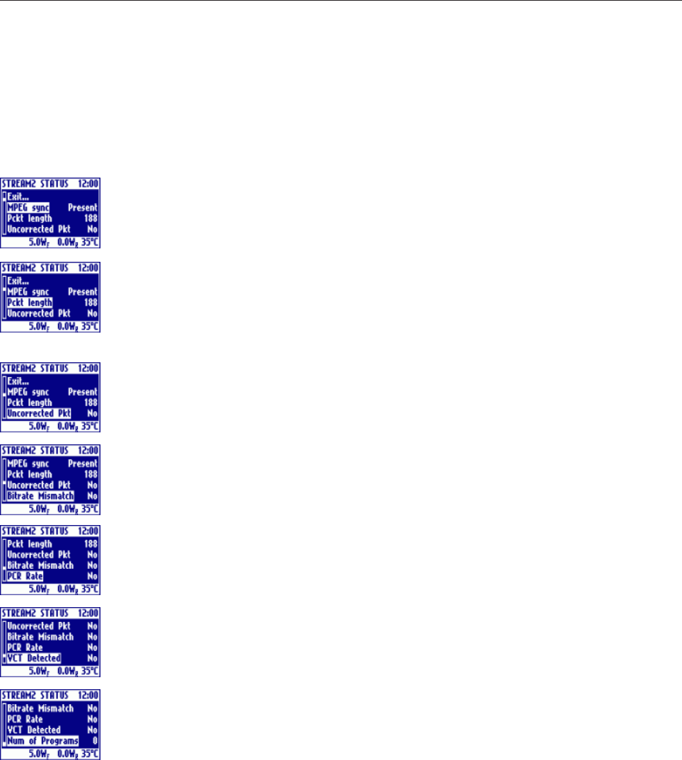
51
- STREAM2 STATUS submenu
MPEG sync (Present, Absent)
If Absent is written, no MPEG sync is detected.
Pckt length (188/204)
This parameter shows the packet length detected on the stream1. The 204-bytes packets
are detected if a true 16-bytes Reed-Solomon code is added to the packet (if the additional
16-bytes are null, the packet length is always indicated as 188).
Uncorrected Pkt (No, Yes)
If this parameter is Yes, incorrect input packet is detected (only in 204 RS coded input
mode).
Bitrate mismatch (No, Yes)
If this parameter is Yes, a bitrate overflow or underflow condition is present (only if bitrate
adaptation is not performed).
PCR Rate (No Yes)
If Err is shown, no PCR is detected over 10 seconds or PCR interval error.
VCT Detected (No, Yes)
This parameter shows if Virtual Channel Table is detected on the Stream 1 over a 10
seconds interval.
Num of Programs
This parameters shows the number of programs present in the Stream1 as indicated in the
Virtual Channel Table.

52
- REFERENCES submenu
10MHz refer. (Int, Ext, ASI)
This parameter shows the 10MHz reference source selection set by the user (Int, Ext, ASI). In
case it is Ext or ASI and if the chosen reference is absent, the modulator automatically uses the
internal reference. This is shown in parentheses. By clicking on this item, the user can change the
10MHz reference source. (See the Synchronization and Clocks paragraph for more
information about the input reference stage of the modulator).
10MHz input (Present, Absent)
This is a read-only parameter that indicates the presence or absence of the external 10MHz
reference. (See the Synchronization and Clocks paragraph for more information about
the input reference stage of the modulator).
LoR Mute (ON, OFF)
When the external reference is absent, it is possible to automatically mute the output after
a configurable timeout. By choosing ON, the automatic mute on lost of reference feature is
enabled. Set this parameter to OFF to not mute the output on lost of reference.
LoR Timeout (00h00’-24h00)
It’s the timeout the transmitter waits before muting the output on lost of reference. If the
LoR Mute parameter is OFF, the timeout is ignored. Set the timeout to 0 to immediately
mute the output on lost of reference.

53
MODULATOR (OK, Err, Temo, No Comm)
If the ATSC Modulator module is correctly working, this read-only parameter shows OK.
If the modulator has an internal error or it doesn't communicate with the control board, it
shows "Err" or "No Comm". If the internal temperature is too high, "Temp" is shown.
Warning! If this parameter isn't OK, a serious malfunction of a core part of the
ATSC TRANSMITTER is present. Be sure to solve this problem before installing the
equipment at the final destination.
Bitrate adapt. (OFF, ON)
If this parameter is set to ON, the bitrate is adapted. If it is set to OFF, the bitrate is not
adapted.
See the TS Input Management paragraph for more information.
PRBS (OFF, PRBS, Sinus)
With this parameter it is possible to activate the PRBS or Single Tone test mode (see the
Test Modes paragraph for more information about the available test modes).
3.4.2 MODULATION MENU

54
Frequency
Click on this item to enter the Frequency submenu to read and/or modify the centre
frequency and the bandwidth of the output signal.
Power
Click on this item to enter the Power submenu to control the output power level and to
configure the AGC (see the AGC: Implementations and Details paragraph for more
informations).
Amplifier
Click on this item to enter the Amplifier submenu to read the internal amplifier status and to
reset the lockout condition (see the Alarms and automations paragraph for more
informations).
Output
Click on this item to enter the Output submenu to read and/or modify some settings related
to the output signal and to the mute configuration.
Precorrection
Click on this item to enter the Precorrection submenu to read and/or modify the precorrection
configuration.
3.4.3 RF MENU
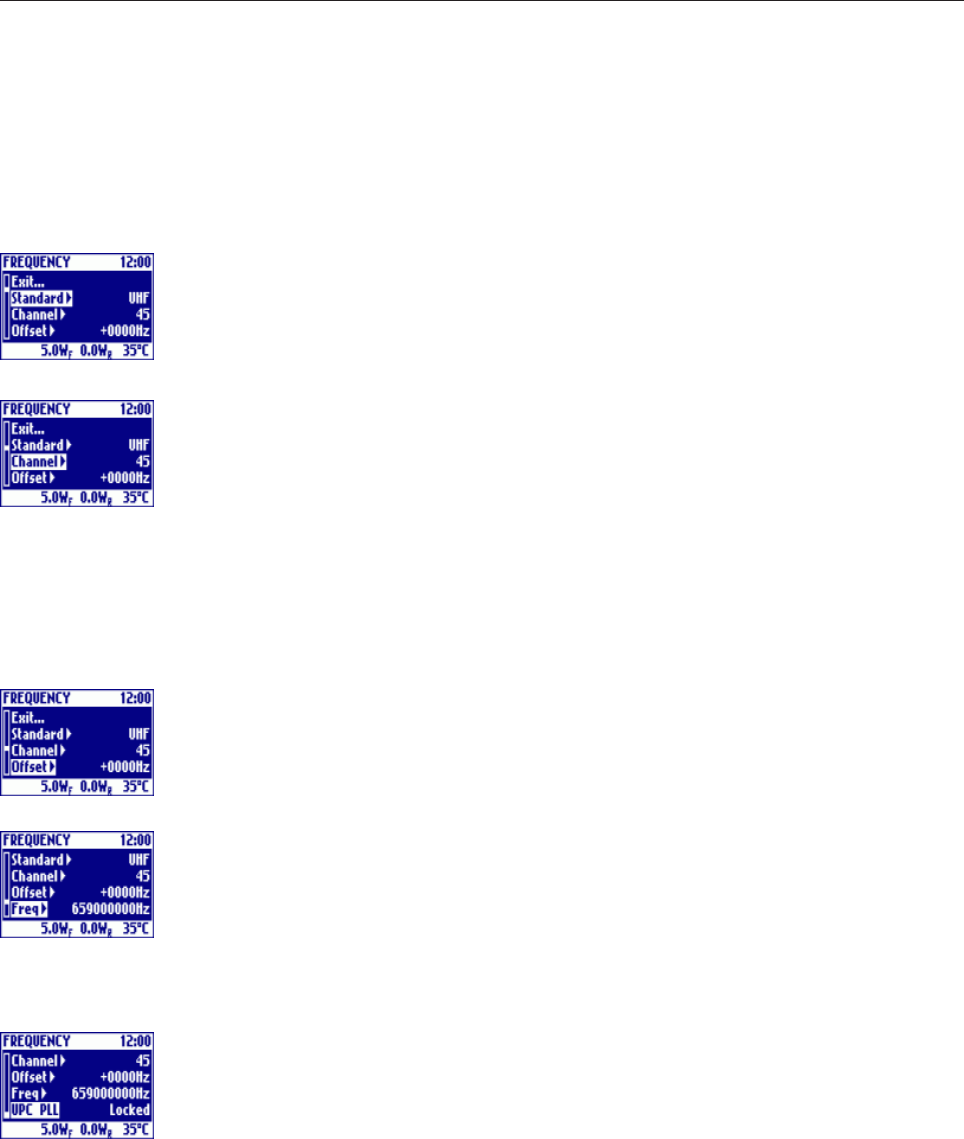
55
- FREQUENCY submenu
Standard ([User], UHF, VHF)
The user can set the output signal frequency by choosing Standard/Channel pair or by
setting a custom frequency. At the time of printing this manual, the available standards are
UHF and VHF. Others may be available with future firmware releases1.
Channel (depending on the selected standard)
The user can set the output signal frequency by choosing Standard/Channel pair or by
setting a custom frequency. At the time of printing this manual, the available standards are
UHF and VHF. Others may be available with future firmware releases. The channels that
can be chosen depend on the selected standard (for example, if UHF standard is selected,
channel can be changed in the 14-69 interval). When a different standard is chosen (for
example, from VHF to UHF), the first channel (in the example, 14) is automatically set.
When a custom frequency is set instead, User appears as the standard and channel and
the channel offset is reset1.
Channel Offset (-9999÷+9999Hz by 1Hz step)
If the frequency is set by using Standatd/Channel pair, it is possible to finely adjust the
center frequency, by setting this parameter. The offset can be negative and positive.
Freq (57÷860MHz by 1Hz step)
The user can set the output signal frequency by choosing Standard/Channel pair or by
setting a custom frequency. The digits of the frequency can be changed one at a time in
the 0-9 range (only the first digit can be changed in the 1-8 range). Click on the knob to
move to the next digit. If a value lower than 57MHz (greater than 860MHz) is set, the
frequency 57MHz (860MHz) will be used instead1.
UPC PLL (Locked, Unlocked)
This read-only parameter shows the status of the up-converter PLL. It can be Locked or
Unlocked1.
1 When a custom frequency is set instead, User appears as the standard and channel and the channel offset is reset. If a frequency
outside the band of the equipment is set, the upconverter PLL can’t lock and the modulator goes in an error condition (for example,
this happens when a UHF channel is set on a VHF transmitter).

56
- POWER submenu
Power Control (Manual, Auto)
This parameter sets the power control mode as either automatic (AGC) or manual.
See the AGC: Implementation and details paragraph for more information.
Warning! For safety operation it is better to set to 0% the power level that is not
selected. For example, if the automatic power control mode is selected, it is better to
set the manual power level to 0%. This way, after changing from automatic to manual,
the output power will safely starts from zero level.
Pwr Level Man (0÷100%)
This parameter sets the operating level of the output power, if manual power control mode
is selected. Rotate the knob to increase/decrease the level in the 0÷100% range.
If the user makes a fast left rotation with a single movement, the power automatically
goes down to 0%. If the user rotates the knob to the right, the autodecrement will be
blocked.
See the AGC: Implementation and details paragraph for more information.
Note that, differently from the usual read/write parameters, when you rotate the
knob the change is immediately active. When you reach the desired value indicated
on the display status bar, click on the knob and choose “Yes” to answer the
confirmation question in order to accept the new power level. Choose “No” to ignore
the new and restore the old level.
Pwr Level Auto (0÷100%)
This parameter sets the operating level of the output power, if automatic power control
mode is selected. Rotate the knob to increase/decrease the level in the 0÷100% range. If
the user makes a fast left rotation with a single movement, the power automatically
goes down to 0%. If the user rotates the knob to the right, the autodecrement will be
blocked.
See the AGC: Implementation and details paragraph for more information.
Note that, differently from the usual read/write parameters, when you rotate the
knob the change is immediately active. When you reach the desired value, click on
the knob and choose “Yes” to answer the confirmation question in order to accept
the new power level. Choose “No” to ignore the new and restore the old level.
Ext AGC (Disabled, Enabled)
You can enable/disable the external AGC by changing the value of this parameter.
Please, be sure to deeply understand the AGC implementation details, before changing
this parameter value. See the AGC: Implementation and details paragraph for
more information.

57
Ext AGC Status (—, Idle, Locked, Lowset, Alarm, Max, Min, Pull-up, Pull-down)
This read-only parameter shows the current status of the external AGC that can be one of
the following:
• —: the external AGC is disabled;
• Idle: the external AGC is stopped (e.g., right after switching on, before the output power
reaches the nominal level);
• Low Set: the external AGC is stopped because external power reading was
too low when the output power was set;
• Alarm: the external AGC is stopped because an Alarm signal from external power amplifier
is detected;
• Locked: the external AGC has reached the desired power level;
• Max/Min: the external AGC is stopped because the correction is too high;
• Pull up/down: the external AGC is moving up or down the driving power level.
See the AGC: Implementation and details paragraph for more information.
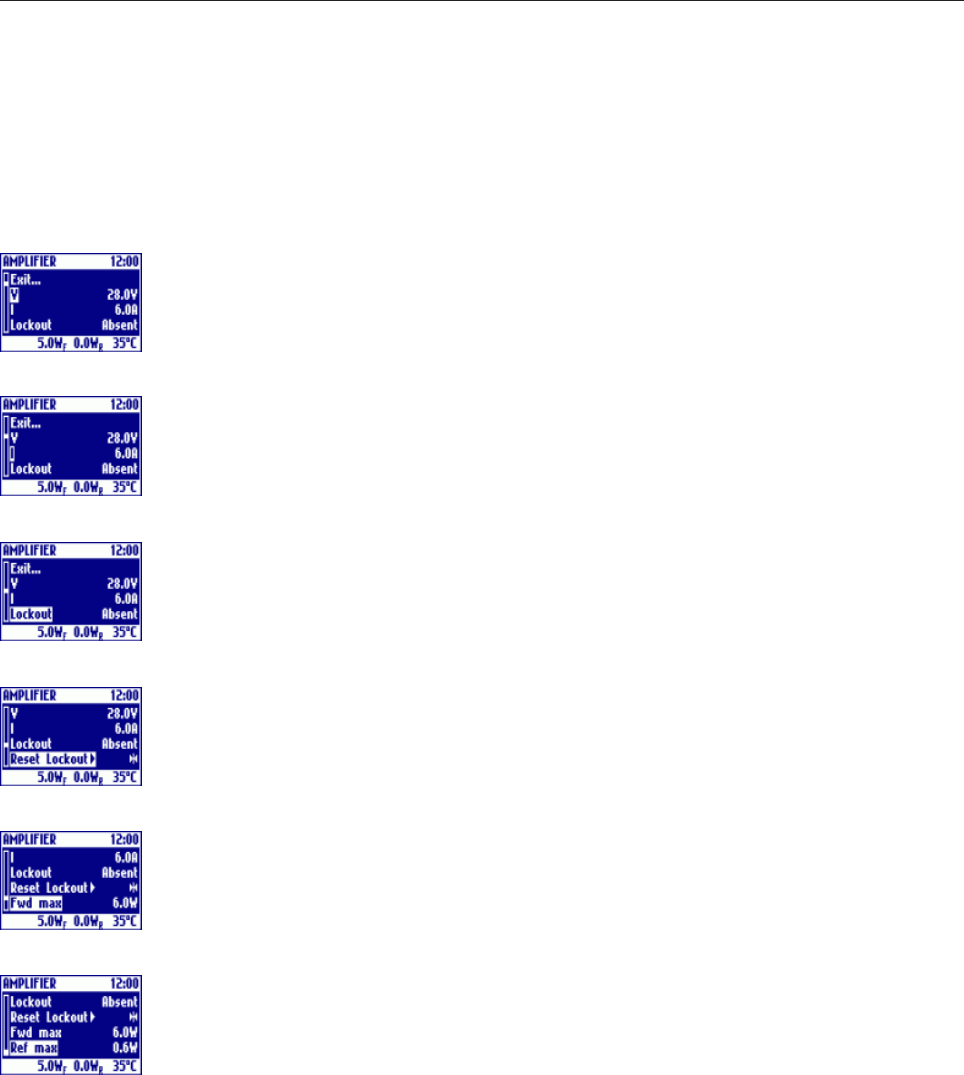
58
V
This is a read-only parameter that shows the voltage of the RF amplifier stage, measured
in Volt. If this value is outside the normal range, an alarm occurs and the value on the
display blinks.
I
This is a read-only parameter that shows the current absorbed by the RF amplifier stage,
measured in Ampere. If this value is outside the normal range, an alarm occurs and the
value on the display blinks.
Lockout (Present, Absent)
This read-only parameter shows whether the lockout condition is present or absent. In
case of presence of lockout, the label blinks (see the Alarms and automation paragraph
for more information).
Reset Lockout
This is an “action” parameter that allows to reset the lockout condition. If the lockout isn’t
present, nothing happens (see the Alarms and automation paragraph for more
information).
Fwd max
This parameter indicates the threshold of the output power. If the output power is higher
than this threshold, an alarm occurs (see the Alarms and automation paragraph for
more information).
Ref max
This parameter indicates the threshold of the reflected power. If the reflected power is
higher than this threshold, an alarm occurs (see the Alarms and automation paragraph
for more information).
- AMPLIFIER submenu
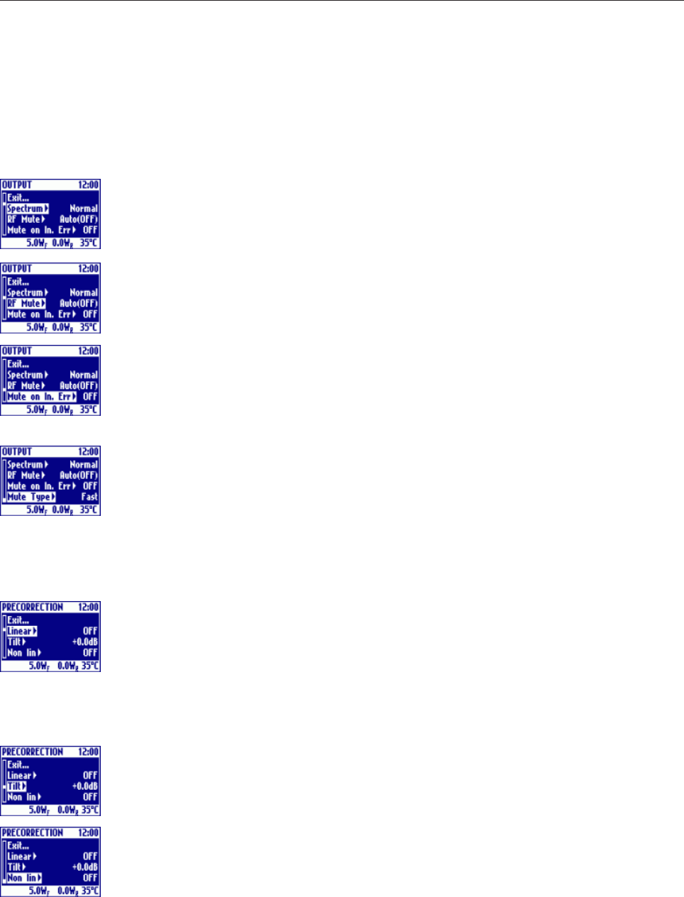
59
Spectrum (Normal, Inverted)
This parameter enables or disables the spectrum inversion.
RF Mute (Auto, ON)
If you set this parameter to ON, the output is muted. If Auto is set, the output can be muted
depending on some conditions. In this case, the current mute status is shown in parenthesis.
Mute on In. Err (ON, OFF)
If this parameter is set to ON, the output will be automatically muted whenever an error on
ASI inputs occurs (for example if the inputs are absent). If it is set to OFF, errors on ASI
inputs don’t affect the output muting.
Mute Type (Fast, Slow)
This parameter sets the mute type. If Fast is set, the mute will be direct (abrupt muting). If
Slow is set, the mute will be progressive.
- OUTPUT submenu
- PRECORRECTION submenu
Linear Precorrection (ON, OFF)
With this parameter it is possible to change the linear precorrection behaviour of the modulator.
If it is set to OFF, the linear precorrection is disabled. If it is set to Null, the linear precorrection
is enabled, but a “null curve” is used. Other linear precorrection curves, up to 2, each characterized
by a different name, could be stored inside the controller. In this case, the user can select one of
them. See the Linear Precorrection paragraph for more information.
Tilt (-1.0÷1.0dB by 0.1dB step)
This parameter is used to add a tilt precorrection on the spectrum. See the Output Signal
paragraph for more information.
Non lin (ON, OFF)
With this parameter it is possible to change the non-linear precorrection behaviour of the modulator. If
it is set to OFF, the non-linear precorrection is disabled. If it is set to Null, the non-linear precorrection
is enabled, but a “null curve” is used. Other non-linear precorrection curves, up to 10, each characterized
by a different name, could be stored inside the controller. In this case, the user can select one of them.
See the Non Linear Precorrection paragraph for more information.
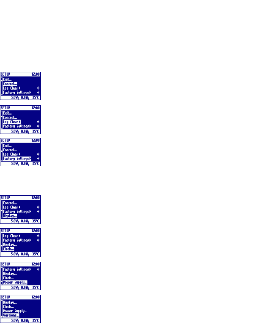
60
Control
Click on this item to enter the Control submenu to configure the remote control and the
password locking.
Log Clear
This is an “action parameter” and it is used to clear the log content. Be sure to read the
latest events before clearing the log. After clearing, it isn’t possible to undelete the events.
Factory Settings
During the test phase of the machine, most of all parameters and adjustments are well
defined and saved in a non-volatile memory. The user can retrieve and load this configuration
by clicking on Factory Settings item menu. Note that after loading the factory settings,
many parameters are changed simultaneously at one time. Please, use this feature with
care.
Display
Click on this item to enter the Display submenu to read and/or modify the backlight and
contrast of the LCD.
Clock
Click on this item to enter the Clock submenu to read and/or change the actual time.
Power Supply
Click on this item to enter the Power Supply submenu to monitor the power supply voltages
status.
Versions
Click on this item to enter the Versions submenu to read all the firmware versions.
3.4.4 SETUP MENU

61
Control (Local, Remote)
The ATSC TRANSMITTER is fully-controllable locally (by using the display and the
knob) or by remote (by using RS232/RS485 serial ports). With this parameter it is possible
to set local control or remote control. When local control is selected, only reading commands
from remote will be answered, while writing commands will be denied. In this case, changing
of settings is possible only locally. If remote control is selected, it will be possible to read
the status locally (display) and from remote (RS232, RS485), but changing of settings will
be possible only by remote. In this case, many parameters will become as read-only type
on the display.
Serial (RS232, RS485)
The remote control can be performed by using a serial port (RS232 or RS485) or a
parallel port (TELEMEASURES). While TELEMEASURES port is always enabled, only
one of the two serial ports must be enabled at any time, because they are mutually exclusive.
If you don’t use remote control, don’t care about this parameter.
TLM out (Alarm, Squelch)
The meaning of the digital output of TLM port (pins 6 and 7) can be changed by the user
in two different modes: Alarm (useful to interface a custom remote control system) and
Squelch (useful to interface a switchover control system).
Password
In order to prevent an unauthorized user from changing the settings of the machine, it is
possible to lock the control by inserting a 5-digits password. When the control is unlocked,
the word “Unlocked” is written as parameter value. Click on this parameter and set a digit
at a time. After changing the last digit and answering “Yes” to the confirmation question, the
control is locked and the word “Locked” appears (the lock symbol is visible on the status
bar too). Now, the user can’t change any setting by using the knob and display. However,
they can continue monitoring the status of the equipment by browsing the menus. Most of
the parameters become as read-only type. When the control is locked, click on this
parameter to insert the same 5-digits password used to lock. If the password is correct,
the control will be unlocked, otherwise the control remains locked.
Contact the Elettronika Customer Service if you forget the password.
- CONTROL submenu
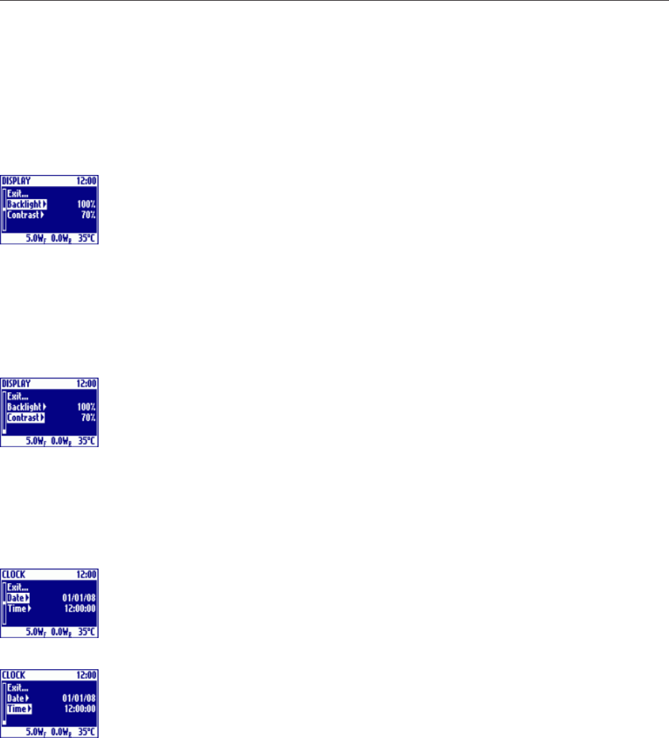
62
- DISPLAY submenu
Backlight (0÷100%)
The graphical LCD has a white-LED backlight. Its intensity can be changed by software
using this parameter. Differently from usual parameters, the modification immediately takes
place when the user rotates the knob. When you reach the desired intensity level, click on
the knob and reply “Yes” to the confirmation question to accept the new value. If you reply
“No”, the value set before entering the parameter is restored. If the user doesn’t use the
knob for more than 1 minute, the display backlight is automatically switched off. Click or
move the knob to switch the LCD backlight on. The knob action (clicking or moving) that
switches on the backlight isn’t used for menu and parameters browsing/settings.
Contrast (0÷100%)
As well as the backlight, the display contrast can be changed by software using this
parameter. Differently from usual parameters, the modification immediately takes place
when the user rotates the knob. When you reach the desired contrast level, click on the
knob and reply “Yes” to the confirmation question to accept the new value. If you reply
“No”, the value set before entering the parameter is restored.
- CLOCK submenu
Date (dd/mm/yy)
With this parameter it is possible to see and change the date stored in the control board. It
is shown in the dd/mm/yy format (dd=day of the month, mm=month, yy=year).
Be sure to set the correct date because it will be stored with log events.
Time (hh:mm:ss)
With this parameter it is possible to see and change the current time stored in the control
board. It is shown in the hh:mm:ss format (hh=hours, mm=minutes, ss=seconds).
Be sure to set the correct time because it will be stored with log events.
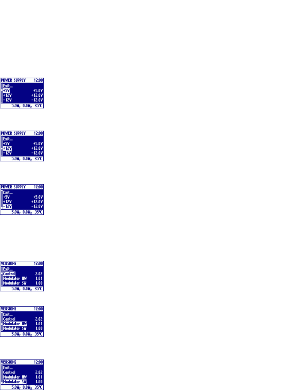
63
- POWER SUPPLY submenu
+5V
This read-only parameter shows the +5V power supply voltage monitored by a voltage
sensor. If this voltage is outside a reasonable range, an alarm occurs and the value starts
blinking on the display (see the Alarms and automation paragraph for more
information).
+12V
This read-only parameter shows the +12V power supply voltage monitored by a voltage
sensor. If this voltage is outside a reasonable range, an alarm occurs and the value starts
blinking on the display (see the Alarms and automation paragraph for more
information).
-12V
This read-only parameter shows the -12V power supply voltage monitored by a voltage
sensor. If this voltage is outside a reasonable range, an alarm occurs and the value starts
blinking on the display (see the Alarms and automation paragraph for more
information).
- VERSIONS submenu
Control
This is the control system version of the ATSC TRANSMITTER. It is composed by two
numbers separated by a dot. Please, indicate this and other versions in the Versions menu
to the technical support in order to simplify the problem solving.
Modulator HW
This is the ATSC Modulator module hardware version. It is composed by two numbers
separated by a dot.
Please, indicate this and other versions in the Versions menu to the technical support in
order to simplify the problem solving.
Modulator SW
This is the ATSC Modulator module software version. It is composed by two numbers
separated by a dot.
Please, indicate this and other versions in the Versions menu to the technical support in
order to simplify the problem solving.

64
By clicking on the LOG icon, you enter the LOG screen. This isn’t a real menu, like the
others, but only a log view. The first event shown is the first event in the log. Move the
knob to scroll the log up/down.
In the titlebar of the small centred window, the number of the event shown and the total
number of events stored in the log are indicated. If the event is an alarm, a bell icon is
drawn on the leftmost side of the titlebar. On the first row there are the date and time at
which the event occurred. On the second line, a short description of the event is shown.
On the left of the small window, a scrollbar is drawn, like in the menus of parameters. The
scrollbar tab gives an idea of position in the list of the displayed event.
Click on the knob while viewing the log to go back to the Main Menu Icons.
3.5 LOG SCREEN
3.6 ALARM SCREEN
By clicking on the ALM icon in the main menu, you enter the ACTIVE ALARMS screen.
This isn't a real menu, like the others, but only a list of alarms that are currently active.
When no alarm is present, "No alarms present." is written on the top of the list.
If at least an alarm is active, the first row of the list is selected. Move the knob to scroll the
alarms list down/up.
On the left, a scrollbar is drawn, like in the menus of parameters. The scrollbar tab gives an
idea position in the list of the selected alarm.
Click on the knob while viewing this screen to go back to the Main Menu Icons.
3.7 FIRMWARE UPGRADE
The control system firmware of the ATSC TRANSMITTER can be upgraded to later versions without removing
the equipment from the rack or replacing any chip. You only need a Windows PC with a RS232 port and a
serial cable.
Carefully follow the steps below to upgrade to a new firmware.
z Obtain EKAFlash software that must be installed on the PC. You can download EKAFlash from the
manufacturer web site (www.elettronika.it). Install EKAFlash on the PC you want to use during the upgrade.
z Connect a straight (pin-to-pin) serial cable (D-SUB9 male on equipment side, D-SUB9 female on PC side)
between the RS232 port of the equipment and a RS232 port of the PC.
z Launch EKAFlash, select the PC RS232 port used for the connection with the equipment, choose the
firmware file (usually with .mhx extension) by pressing the "..." button and click on the Download button.
z Switch off the equipment and switch it on again.
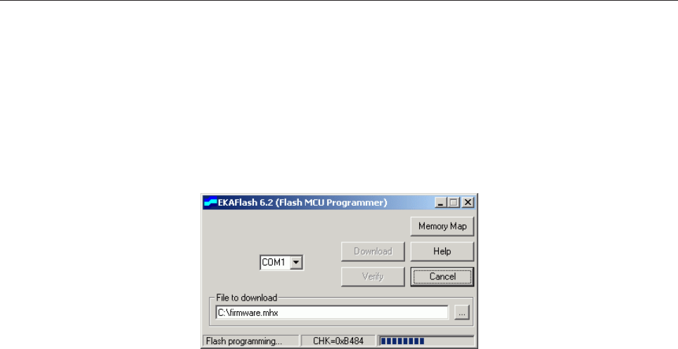
65
The upgrade of the firmware should start. After upgrading, the equipment will automatically start with the new
firmware.
Warning! Keep in mind that the firmware upgrade is a critical task. You could have a non-working machine
if the upgrading process doesn't end with success or if you download a wrong firmware.
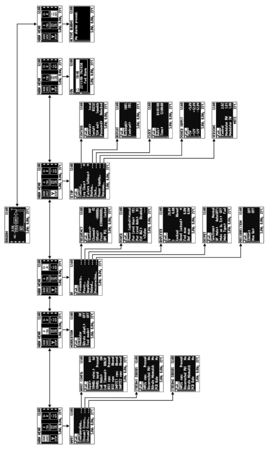
66
ATSC Transmitter Menu Map

67
Section 4 - Diagram
Contents:
- APD043A UHF ATSC TRANSMITTER Cable Diagram
- APD047A VHF-III ATSC TRANSMITTER Cable Diagram
- APD045A VHF-I ATSC TRANSMITTER Cable Diagram
- APD043A_APD047A_APD045A Component list
- Modules description
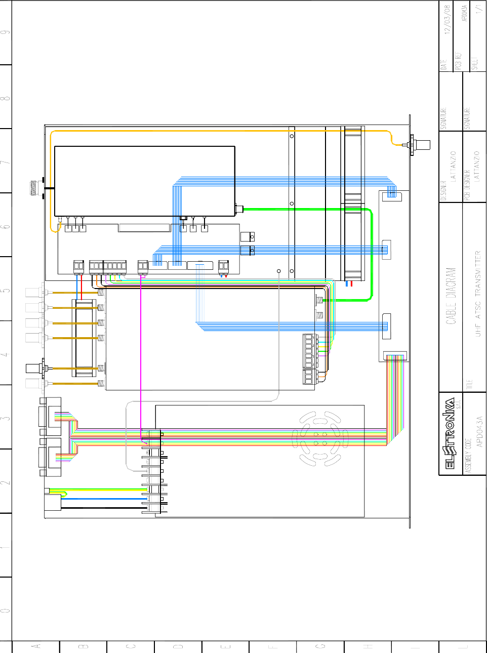
68
CTRL
TP8
TP7
GATE
+28V
TP4
TP3
+5V
REF
TP2
FWD
TP1
SP-320-27 SWITCHING POWER SUPPLY
20 POLES
FLAT CABLE
E0064
GND
GND
12Vdc
DISPLAY BOARD
16 POLES
FLAT CABLE
J3
J2
SCH0135A
J5
RF OUT
RX
TX
RX-
RX
GND
TX-
TX
RS232 RS485 RF MONIT.
TO SCH0388B
10 POLES
FLAT CABLE
GND
AC FILTER
L
10MHz OUT
ATSC UHF MODULATOR MODULE
NGND -V +V
TELEMEASURES
10MHz IN
RS485
POWER SUPPLY BOARD
SCH0388B
A1592
J9
J8
J7
J6
J5
J4
ASI1 ASI2 SMPTE1 SMPTE2
J1
J2
10 POLES
FLAT CABLE
J1
RF MONITOR
MTF0116A
RF AMPLIFIER MODULE
RF IN
CTRL
GATE
+28V
RF MONITOR
+5V
REF
FWD
RF OUT
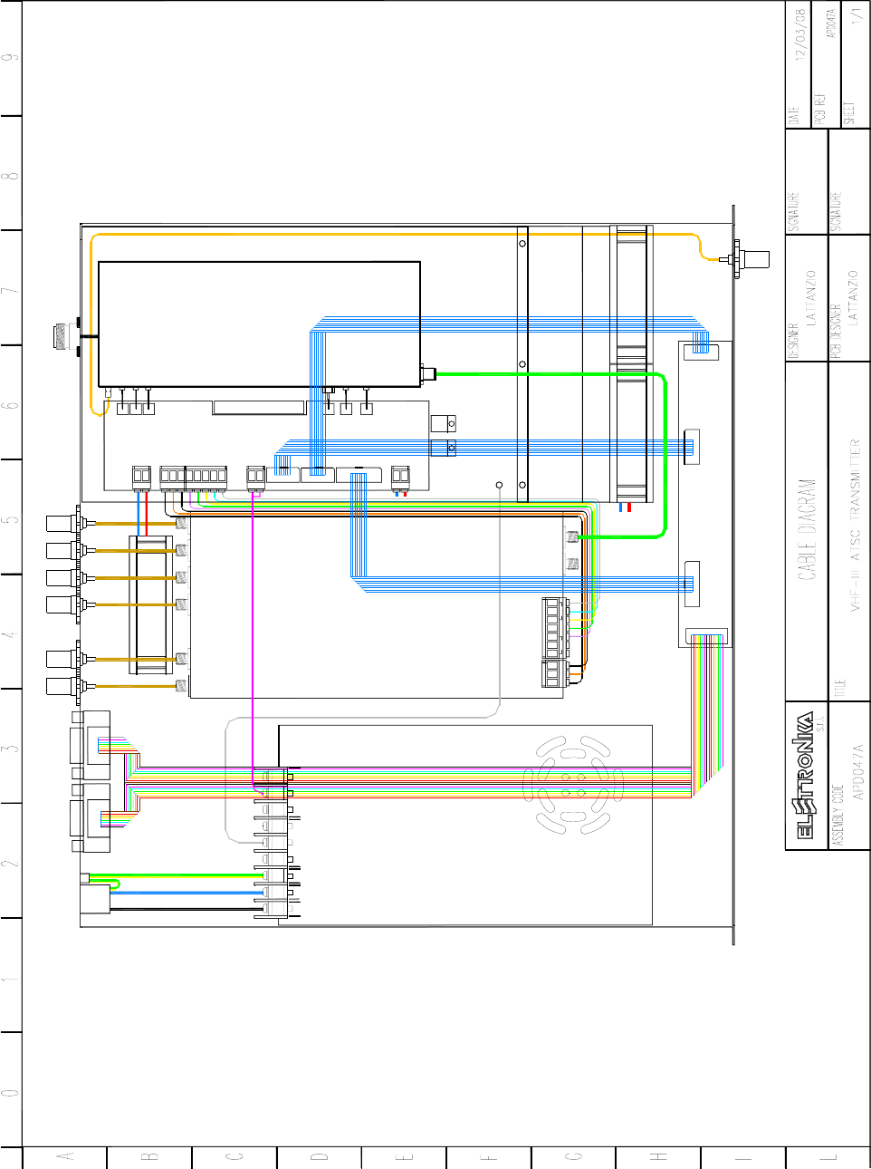
69
AC FILTER
TELEMEASURES
GNDNL +V-V
SMPTE2SMPTE1ASI2ASI1
SCH0388B
POWER SUPPLY BOARD
10MHz IN 10MHz OUT
RS485
FWD
TP1
J1
TP2
REF
+5V
TP3
J2
ATSC VHF-I / III MODULATOR MODULE
A1703
J4
J5
J6
TP4
+28V
RF MONITOR
FWD
RF OUT
REF
+5V
RF AMPLIFIER MODULE
MTF0118A
+28V
SP-320-27 SWITCHING POWER SUPPLY
E0064
TP8
J7
GATE
TP7
J8
CTRL
J9
TX
TX-
GND
RX
RX-
TX
RX
12Vdc
GND
GND
RS232 RS485
GND
RF OUTRF MONIT.
10 POLES
FLAT CABLE
FLAT CABLE
20 POLES
FLAT CABLE
16 POLES
J3
TO SCH0388B
SCH0135A
DISPLAY BOARD
J2 J5
CTRL
GATE
RF IN
FLAT CABLE
10 POLES
J1
RF MONITOR
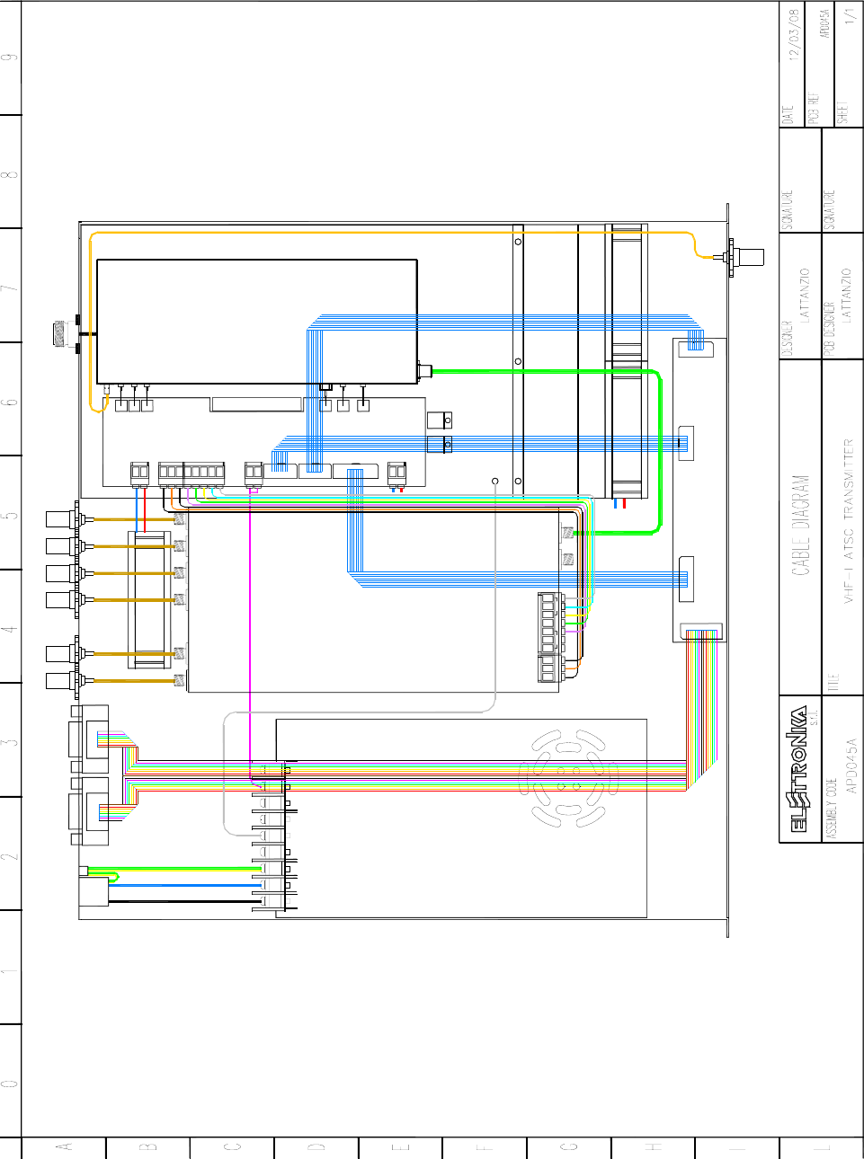
70
AC FILTER
TELEMEASURES
GNDNL +V-V
SMPTE2SMPTE1ASI2ASI1
SCH0388B
POWER SUPPLY BOARD
10MHz IN 10MHz OUT
RS485
FWD
TP1
J1
TP2
REF
+5V
TP3
J2
ATSC VHF-I / III MODULATOR MODULE
A1703
J4
J5
J6
TP4
+28V
RF MONITOR
FWD
RF OUT
REF
+5V
RF AMPLIFIER MODULE
MTF0125A
+28V
SP-320-27 SWITCHING POWER SUPPLY
E0064
TP8
J7
GATE
TP7
J8
CTRL
J9
TX
TX-
GND
RX
RX-
TX
RX
12Vdc
GND
GND
RS232 RS485
GND
RF OUTRF MONIT.
10 POLES
FLAT CABLE
FLAT CABLE
20 POLES
FLAT CABLE
16 POLES
J3
TO SCH0388B
SCH0135A
DISPLAY BOARD
J2 J5
CTRL
GATE
RF IN
FLAT CABLE
10 POLES
J1
RF MONITOR

71
Elettronika Code Description Qty
E0064 SP-320-27 DI SWITCHING POWER SUPPLY 1
MTF0116AR0 5W RMS UHF AMPLIFIER MODULE 1 (APD043A)
MTF0118AR0 5W RMS VHF-III AMPLIFIER MODULE 1 (APD047A)
MTF0125AR0 5W RMS VHF-I AMPLIFIER MODULE 1 (APD045A)
DET0531I DET0531AR1 FAN CONVEYER 1
DET0600 DET0600R1 MECHANICAL DETAIL 1
07613 PAPST BLOWER 3
07602 BLOWER GRID 3
A1592 ATSC UHF MODULATOR MODULE 1
A1703 ATSC VHF-I/III MODULATOR MODULE 1 (APD047A_APD045A)
PAN0187R0P PAN0187R0 FRONT PANEL 1
02700 16 WAY FEMALE CONNECTOR 2
02701 16 WAY MALE CONNECTOR 1
02699 10 WAY MALE CONNECTOR 4
02867 20 WAY FEMALE CONNECTOR 1
02695 DB9 CONNECTOR FOR IU008059 CABLE 2
02518 SMB SOCKET FOR RG174 CABLE 1
02519 SMA SOCKET FOR RG174 CABLE 6
05069 TOROIDAL FILTER 1
DET0670 DET0670R0 MECHANICAL DETAIL 1
DET0315 DET0315R0 2U HANDLE KIT 2
08502 RG 316 50Ω CABLE 1.40
08521 RG 179 75Ω CABLE 0.60
SCH0135AR1 DISPLAY BOARD 1
02035 BNC FEMALE CONNECTOR FOR RG316 CABLE 8
DET1322R1P DET1322R1P MECHANICAL DETAIL 1
DET1323R0P DET1323R0P CONVEYER 1
DET0876I DET0876R1 POWER SUPPLY CONVEYER 1
CON0352R2S CON0352R2 BOX 1
CON0353R0P CON0353R0P COVER 1
FLR0002 FUSE DRAWER 1
FLR0003 AC FILTER 1
FUS02A 2A FUSE 2
02503A 90° SMA SOCKET FOR RG 316 CABLE 2
V0760 BLACK PLASTIC TAP 2
Component list APD043A - APD047A - APD045A

72
This page is intentionally blank

73
CONTROL BOARD AND DISPLAY SCH0135AR1
DESCRIPTION
The Controller module, located on the right side of the DIGITAL TRANSMITTER, is the user interface of
the whole modulator. It gathers the data from all the sections of the modulator, processes them by means of a
16bit flash micro-controller by Fujitsu and makes them available to the user both through the local interface,
composed by a display and a knob, and the remote interface made up by the serial port (either the RS232 on
the front or the RS485 on the back, as selected) or the interface of the telemeasuring connector.
The acquisition and setting of all the concerned parameters is made in two different ways. Analog measures
reach the board from the individual modules as voltages, are conditioned on the board and then converted by
an internal A/D converter in the micro.
The remaining parameters are gathered through a 2-wire RS485 interface, with the modulator. The display
board acts as master on this 485 bus. Besides it is provided with an RTC and a non-volatile memory on an
internal I2C bus.
- Dip-Switch
The display board is provided with 4 dip-switches. The dip-switches 3 and 4 are used to program the flash
memory of the flash micro-controller by Fujitsu, in detail:
DIP3: On DIP4: Off Boot Programming
DIP3: Off DIP4: On Run or Firmware Programming
The "Boot Programming" configuration is only for BIOS programming purposes.
Once the BIOS has been programmed, the firmware has to be programmed at least once in order to use the
board. The firmware programming and the normal operation of the board are obtained with the same position
of the dip switches.
For more detail on Firmware upgrade please refer to the "Firmware Upgrade" section.
TECHNICAL CHARACTERISTICS
Flash ROM 256kByte
RAM 6kByte
EEPROM 64kBit
Serial interfaces 2xRS485 or 1xRS485 + 1xRS232
Graphic display 128x64pixel blue with white LED backlight
Encoder Mechanical with push button
Clock and Calendar Lithium battery backup
Telemeasures Output: FWD, REF, Alarm/Mute
Input: Remote ON/OFF
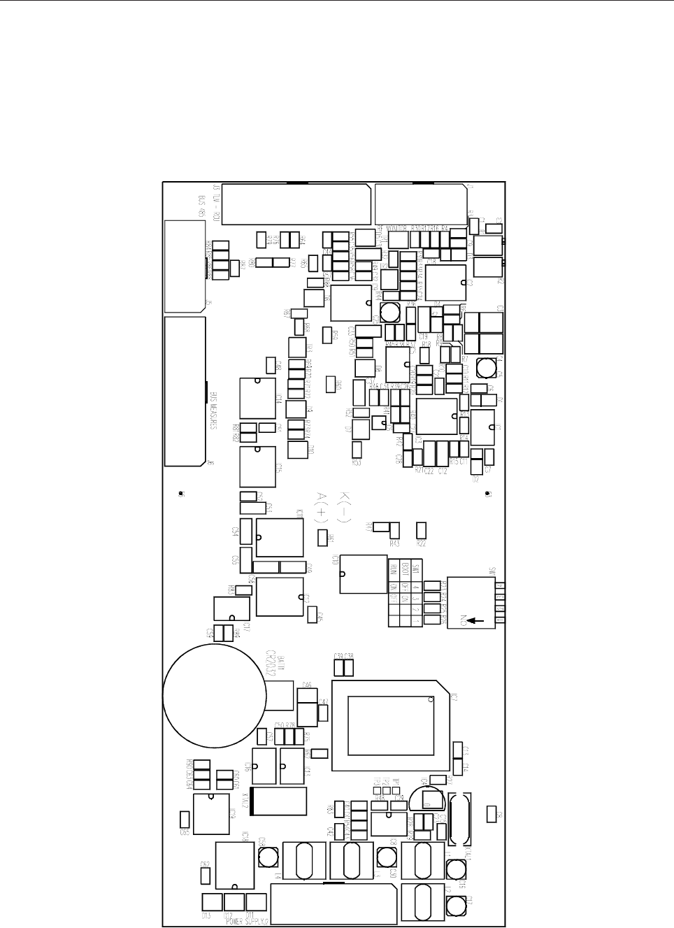
74
SCH0135AR1 Top layer Component layout
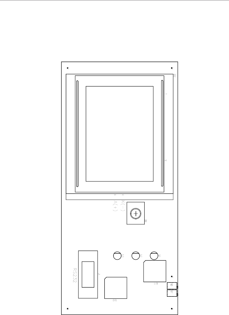
75
SCH0135AR1 Bottom layer Component layout

76
SCH0135AR1 COMPONENT LIST
Part Name/Number Description Qty. Comps. Page 1/2
BATT BH001RB 3093_90 03093 03090 BATTERY HOLDER 1 BATT1
CC 100nF-S 01065E 01065E Y5V 0805 COND 26 C7-8, C13, C18, C21, C23-24, C26, C29, C32,
C34-36, C38-39, C43, C45, C47-48, C50-52,
C57, C59, C62, C65
CC 10nF-S 01053A 01053A SMD 0805 COND 1 C9
CC 15pF-SS 01088A SMD 0805 COND 4 C10, C14-15, C20
CC 1nF-S 01096A 01096A SMD 0805 COND 9 C1-2, C27-28, C44, C60-61, C63-64
CC 1uF100V-S 01760A 01760A Y5V 1206 COND «50V» 9 C19, C31, C33, C37, C49, C53-56
CC 220nF-S 01069B 01069B Y5V 0805 COND 3 C40-42
CC 47pF-S 01090B 01090B SMD 0805 COND 2 C6, C11
CE 10uF16V-S 01626B TANT. ELETTR SMD CO 2 C12, C22
CE 10uF16V-S 01776A 01776A ELETTR SMD COND 4 C5, C17, C30, C58
CE 22uF25V-S 01632 TANT. ELETTR SMD CON 1 C3
CE 47uF 16V-S 01636A TANT. ELETTR SMD CO 1 C46
CE 4u7F35V-S 01623A 01623A TANT. ELETTR SMD CO 1 C4
CE 4u7F35V-S 01774A 01774A ELETTR SMD COND 1 C25
CE D4 N. M. N. M. ELETTR SMD COND 1 C16
D BAS85-S 03024 SMD DIODE SCHOTTKY 3 D1-3
D BAS85-S N. M. N. M. 1 D4
D BAT54S 03199 SMD SCH. DIODE A-K T 8 D5-6, D8-13
D LM431-S 04614 SMD ADJ. ZENER 1 D7
DIS MGLS12864T 03083A 128x64 DOT (BLUE-LED) 1 DIS1
DL LEDG3 03053 03053 GREEN LED DIODE 3mm 1 DL1
DL LEDR3 03058 03058 RED LED DIODE 3mm 1 DL3
DL LEDY3 03051 03051 YEL. LED DIODE 3mm 1 DL2
EN ENCODER DDM427 03095 ENCODER 1 EN1
IC 24LC64 04815 04815 SMD INTEG CIRCUIT 1 IC13
IC 74HC00-S 4762A 4762A SMD INTEG CIRCUIT 1 IC15
IC AD5312BRM-S 04592A SMD INTEG CIRCUIT 1 IC6
IC CD4053BC-S 04710A 04710A SMD INTEG CIRCUIT 2 IC12, IC18
IC LM324M-S 04658A 04658A SMD INTEG CIRCUIT 1 IC2
IC LM358M-S 04660 04660 SMD INTEG CIRCUIT 2 IC5, IC8
IC LMC6484-S 04634 SMD INTEG CIRCUIT 3 IC3, IC9, IC19
IC M41T56 04611 04611 SMD INTEG CIRCUIT 1 IC16
IC MAX232-S 04804B 04804B SMD INTEG CIRCUIT 1 IC11
IC MAX3080-S 04770 04770 SMD INTEG CIRCUIT 1 IC14
IC MAX942CSA-S 04572 SMD INTEG CIRCUIT 1 IC1
IC MB90F543PF 04596 SMD INTEG CIRCUIT 1 IC7
IC MPC100T-450I-TT 04577 SMD INTEG CIRCUIT 1 IC4
IC SN75176B-S 04720 04720 SMD INTEG CIRCUIT 1 IC17
IC ULN2003A 4870 04870 SMD INTEG CIRCUIT 1 IC10
IND MS85 10uH-S 04948 INDUCTOR 2,7 A 3 L2-4
IND MS85 N. M. INDUCTOR N. M. 1 L1

77
Part Name/Number Description Qty. Comps. Page 2/2
J DB9_F-0° LT 02794 PCB CON. DB9 LONG T 1 J4
J FC-10P 02697-02699 02697+02699 PCB CON. POL 2 J1, J5
J FC-16P 02701-02700 02701+02700 PCB CON. POL 1 J2
J FC-20P 02868-02867 02868+02867 PCB CON. POL 2 J3, J6
R 0805 N. M. N. M. RES 1/4W 5% SMD 08 4 R6, R34, R65, R68
R 0R0-SS 00001A RES 1/4W 5% SMD 0805 1 R35
R 100K-S 00065C 00065C RES 1/4W 5% SMD 0805 7 R3-4, R8, R16, R36, R72, R74
R 100R-S 00029B 00029B RES 1/4W 5% SMD 0805 6 R49-50, R60, R71, R73, R90
R 10K-S 00053C 00053C RES 1/4W 5% SMD 0805 28 R11, R19, R22-27, R30-33, R38, R41, R43,
R44-45, R47-48, R62, R67, R69-70, R81-83,
R88-89
R 10R-S 00017B 00017B RES 1/4W 5% SMD 0805 2 R7, R61
R 150R-SS 00031C RES 1/4W 5% SMD 0805 2 R77, R85
R 18K-S 00056A 00056A RES 1/4W 5% SMD 0805 1 R39
R 1K0-S 00041C 00041C RES 1/4W 5% SMD 0805 12 R40, R42, R46, R52-53, R56-57, R64, R75,
R78-79, R87
R 1K5-SS 00043C RES 1/4W 5% SMD 0805 4 R76, R80, R84, R86
R 1M-SS 00077B RES 1/4W 5% SMD 0805 1 R17
R 22K-S 00057C 00057C RES 1/4W 5% SMD 0805 3 R12, R20, R28
R 2K2-S 00045C 00045C RES 1/4W 5% SMD 0805 2 R13-14
R 330R-S 00035C 00035C RES 1/4W 5% SMD 0805 2 R37, R66
R 3K9-SS 00048C RES 1/4W SMD 0805 1 R58
R 470K-SS 00073B RES 1/4W 5% SMD 0805 4 R5, R15, R21, R55
R 470R-S 00037C 00037C RES 1/4W 5% SMD 0805 2 R9-10
R 47K-S 00061C 00061C RES 1/4W 5% SMD 0805 2 R54, R63
R 5K6-S 00050C 00050C RES 1/4W 5% SMD 0805 1 R29
R 680R-SS 00039C RES 1/8W 1% SMD 0805 3 R18, R51, R59
RL TQ2-SA-12 07569A 07569A RELE 2 RLY1-2
RV 10K-3266X 00807 00807 VARIABLE RESISTOR 2 R1-2
SW SWITCH-4DIP 90° 07531A PCB DIP SWITCH 90° 1 SW1
TR BC848 03457 03457 NPN SMD TRANSISTOR 3 TR1-3
XTAL 32.768k-S 05146 05146 QUARTZ 1 XTAL2
XTAL 4MHz-S 05101A 05101A QUARTZ 1 XTAL1
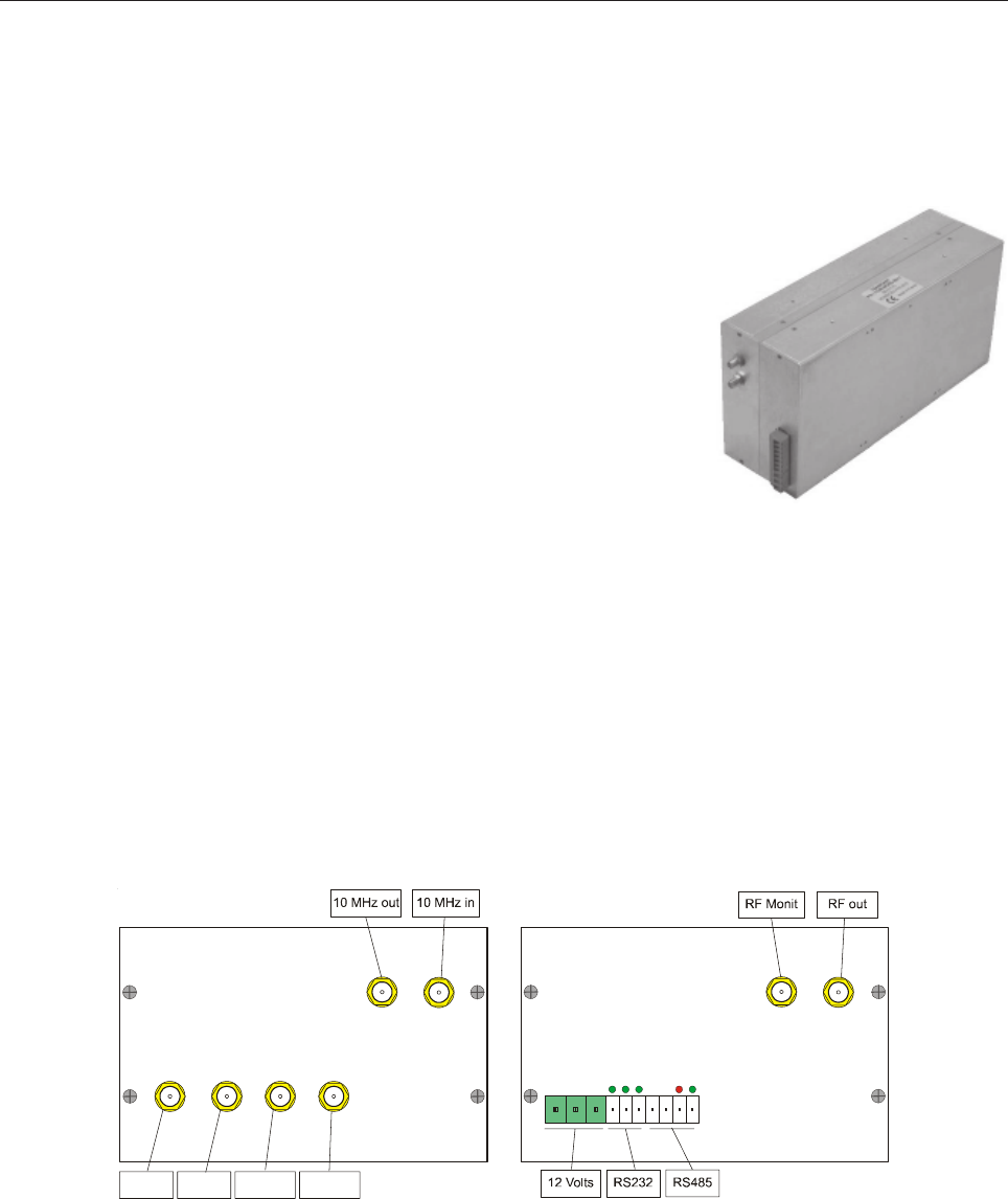
78
ATSC UHF MODULATOR MODULE A1592
DESCRIPTION
The ATSC UHF Modulator module is a very high performance Digital TV
modulator, fully compliant to the A/53 recommendation.
The module includes highly linear 8-VSB modulation capability, excellent
MER value, ASI and SMPTE-310M compatibility, digital pre-correction,
low phase noise and high performance up converter.
MAIN FEATURES
- ATSC 8-VSB Modulator compliant with A/53 recommendation
- SMPTE-310M and ASI inputs
- Powerful TS input management (redundancy, automatic switching, bit rate adaptation, ...)
- Very high performance modulation (MER, RF stability, ...)
- Integrated digital pre-corrector (linear and non-linear)
- Low phase noise synthesizer for a high performance agile UHF output
- UHF Band IV & V output
CONNECTORS
ASI1 ASI2
SMPTE1 SMPTE2

79
ATSC VHF-I/III MODULATOR MODULE A1703
DESCRIPTION
The ATSC VHF Modulator module is a very high performance Digital TV
modulator, fully compliant to the A/53 recommendation.
The module includes highly linear 8-VSB modulation capability, excellent
MER value, ASI and SMPTE-310M compatibility, digital pre-correction,
low phase noise and high performance up converter.
MAIN FEATURES
- ATSC 8-VSB Modulator compliant with A/53 recommendation
- SMPTE-310M and ASI inputs
- Powerful TS input management (redundancy, automatic switching, bit rate adaptation, ...)
- Very high performance modulation (MER, RF stability, ...)
- Integrated digital pre-corrector (linear and non-linear)
- Low phase noise synthesizer for a high performance agile VHF output
- VHF Band I & III output
CONNECTORS
ASI1 ASI2
SMPTE1 SMPTE2

80
5W UHF RMS AMPLIFIER MODULE MTF0116AR0
DESCRIPTION
The MTF0116A is the final stage of the 5W UHF RMS of the transmitter, based on LDMOS technology. It
includes the final stage itself (SCH0417A), its cooling heatsink, and an interface board (SCH0388B) which allows
to control the forward power, the reflect power, the Gain and the temperature. The final amplifier is provided with
a GATE control to inhibit the power output, a circuit to monitor the output and the needed circuits to read the output
forward and reflected power. The power reading is an RMS measurement.
TECHNICAL CHARACTERISTICS
Output Power 5W RMS
Frequency Range 470 - 860MHz
Gain 43dB ±0.5
Power Supply 28V ±2%
Total Quiescent Current (cold) 6A ±5%
Output Impedance 50Ω
Input Impedance 50Ω
Input Return Loss >15dB
MTF0116A COMPONENT LIST
Part Name Code Description Qty
00432 50Ω 60W TERMINAL RESISTOR 1
00664 LM35DT THERMAL SENSOR 1
01400 BYPASSING CAPACITOR 2
01403 BYPASSING CAPACITOR 5
02209B PANEL MOUNTING N SOCKET 1
02512 SMA SOCKET 1
02515 SMB SCREW cod. R114313000 1
03469 BLF1043.112 TRANSISTOR 2
04031A MRF363ALR5 LDMOS TRANSISTOR 2
04340 LM 317T VOLTAGE REGULATOR 1
07683 1.0mm SILVER WIRE 0.20
08502 RG 316 50Ω CABLE 0.10
C0171 AWG22 TEFLON CABLE 0.25
DET1026 DET1026R0 MECHANICAL DETAIL 2
DET1320R1P DET1320R1P MECHANICAL DETAIL 1
DET1330R2P DET1330R2P HEAT SINK MODULE 1
SCA0115 SCA0115R0 COVER 1
SCA0128R1B SCA0128R1B RF AMPLIFIER MODULE BOX 1
SCH0388BR1 POWER SUPPLY INTERFACE BOARD 1
SCH0417AR0 5W RMS UHF AMPLIFIER MODULE 1
V0771 3x5 MALE/FEMALE SPACER 4
TRANSISTOR NAME BIAS CURRENT
TR1 Pre-Driver BLF1043 0.4A
TR2 Driver BLF1043 0.6A
TR3 Output Stage MRF373 2.5A
TR4 Output Stage MRF373 2.5A
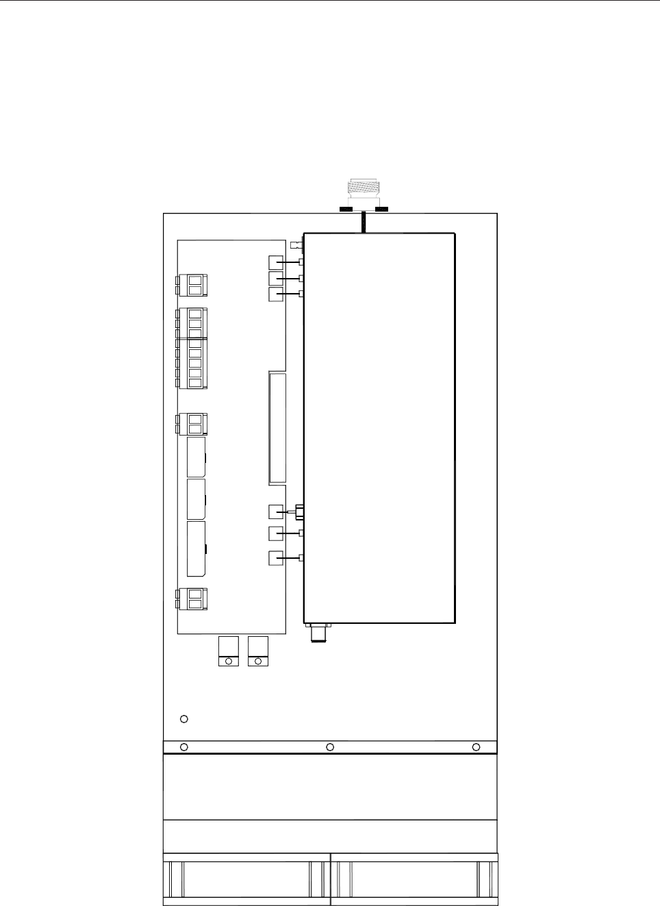
81
MTF0116AR0 Component layout
SCH0388B
POWER SUPPLY BOARD
J2
J1
J4
J5
J6
J7
RF OUT
TP1
FWD
RF MONITOR
FWD
TP2
REF
+5V
TP3
REF
+5V
RF AMPLIFIER MODULE
MTF0116A
TP4
+28V +28V
J9
J8
GND
GATE
TP7
TP8
CTRL
GATE
CTRL
RF IN
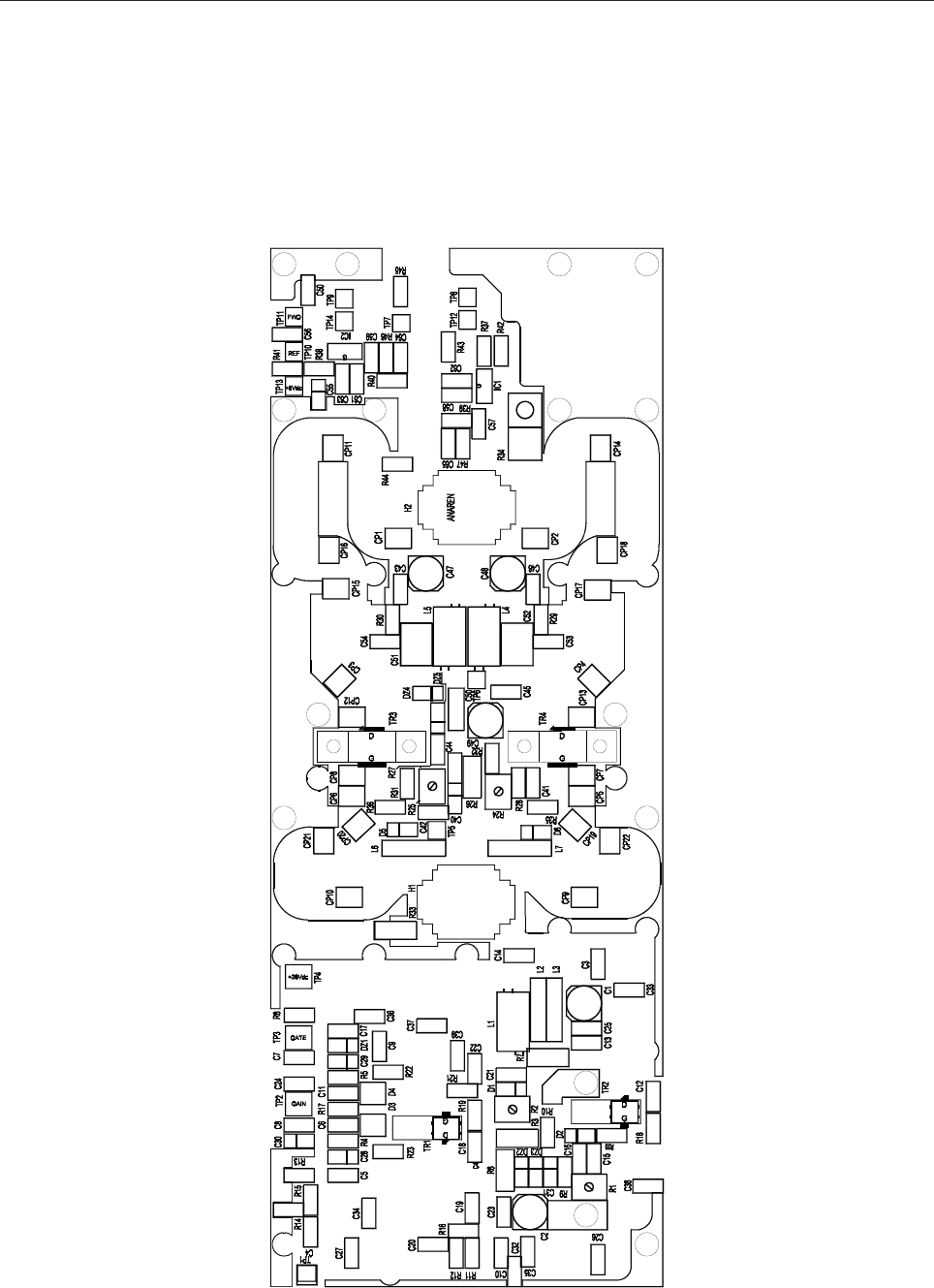
82
SCH0417AR0 Component layout

83
SCH0417AR0 COMPONENT LIST
Part Name/Number Description Qty. Comps.
CC 100nF-S 01065C 01065C Y5V 1206 CAPACITOR 4 C43-46
CC 100pF-S 01092 01092 SMD 1206 CAPACITOR 2 C53-54
CC 1nF-S 01096 01096 SMD 1206 CAPACITOR 2 C41-42
CC 1uF 100V 01077A CERAMIC CAPACITOR 2 C51-52
CC 470nF 63V-S 01073 POLIESTER SMD CAPAC. 1 C50
CE 10uF16V-S 01626B TANT. ELET. CAPACITOR 1 C40
CE 10uF50V-S 01779A 01779A ELET. SMD CAPACITOR 3 C47-49
CP 10pF-S CHIP CHB 2 CP7-8
CP 12pF-S CHIP CHB 2 CP5-6
CP 15pF-S 01121 CHIP CHB 4 CP1-4
CP 1p8F-S 01102A CHIP CHB 4 CP11-14
CP 47pF-S 01130 CHIP CHB 2 CP9-10
CP 5p6F-S 01109 CHIP CHB 2 CP21-22
CP 6p8F-S CHIP CHB 6 CP15-20
D 1N4148-S 03002 03002 SMD DIODE 2 D5-6
DZ 3V9-S 03134 SMD ZENER DIODE 2 DZ4-5
H ANAREN 1F1304-3 05368 HIBRID COUPL. ANAREM 2 H1-2
IND CBD8 05072 05072 INDUCTOR 2 L6-7
IND VK200 05013 05013 INDUCTOR 2 L4-5
R 10R-S 00017A 00017A RES 1/4W 5% SMD 1206 2 R29-30
R 1K5-S 00043A 00043A RES 1/4W 5% SMD 1206 2 R35-36
R 22K-S 00057A 00057A RES 1/4W 5% SMD 1206 2 R31-32
R 3K3-1W-S 00400 RES 1W 5% SMD 2512 1 R26
R 47K-S 00061A 00061A RES 1/4W 5% SMD 1206 2 R27-28
R 47R-1W-S 00384 RES 1W 5% SMD 2512 1 R33
R 50R 60W TERM 00432 50Ω 60W RF TERM 1 R34
RV 50K-S-H/S 00797 00797 SMD VARIABLE RESISTOR 2 R24-25
TR MRF373A-S 04031A LDMOS TRANSISTOR 2 TR3-4
84
5W VHF-III RMS AMPLIFIER MODULE MTF0118AR0
DESCRIPTION
The MTF0118A is the final stage of the 5W VHF RMS of the transmitter, based on MOS technology. It includes
the final stage itself (SCH0436A), its cooling heatsink, and an interface board (SCH0388B) which allows to control
the forward power, the reflect power, the Gain and the temperature. The final amplifier is provided with a GATE
control to inhibit the power output, a circuit to monitor the output and the needed circuits to read the output forward
and reflected power. The power reading is an RMS measurement.
TECHNICAL CHARACTERISTICS
Output Power 5W RMS
Frequency Range 170 - 230MHz
Gain 43dB ±0.5
Power Supply 28V ±2%
Total Quiescent Current (cold) 2.6A
Output Impedance 50Ω
Input Impedance 50Ω
Input Return Loss >15dB
MTF0118A COMPONENT LIST
Part Name Code Description Qty
00432 50Ω 60W TERMINAL RESISTOR 1
00664 LM35DT THERMAL SENSOR 1
01400 BYPASSING CAPACITOR 2
01403 BYPASSING CAPACITOR 5
02209B PANEL MOUNTING N SOCKET 1
02512 SMA SOCKET 1
02515 SMB SCREW cod. R114313000 1
03469 BLF1043.112 TRANSISTOR 2
04031A MRF363ALR5 LDMOS TRANSISTOR 1
04340 LM 317T VOLTAGE REGULATOR 1
07683 1.0mm SILVER WIRE 0.20
08502 RG 316 50Ω CABLE 0.10
C0171 AWG22 TEFLON CABLE 0.25
DET1026 DET1026R0 MECHANICAL DETAIL 2
DET1320R1P DET1320R1P MECHANICAL DETAIL 1
DET1330R2P DET1330R2P HEAT SINK MODULE 1
SCA0115 SCA0115R0 COVER 1
SCA0128R1B SCA0128R1B RF AMPLIFIER MODULE BOX 1
SCH0388BR1 POWER SUPPLY INTERFACE BOARD 1
SCH0436AR0 5W RMS VHF AMPLIFIER MODULE 1
V0771 3x5 MALE/FEMALE SPACER 4
TRANSISTOR NAME BIAS CURRENT
TR1 Pre-Driver BLF1043 0.4A
TR2 Driver BLF1043 0.6A
TR3 Output Stage MRF373 1.5A
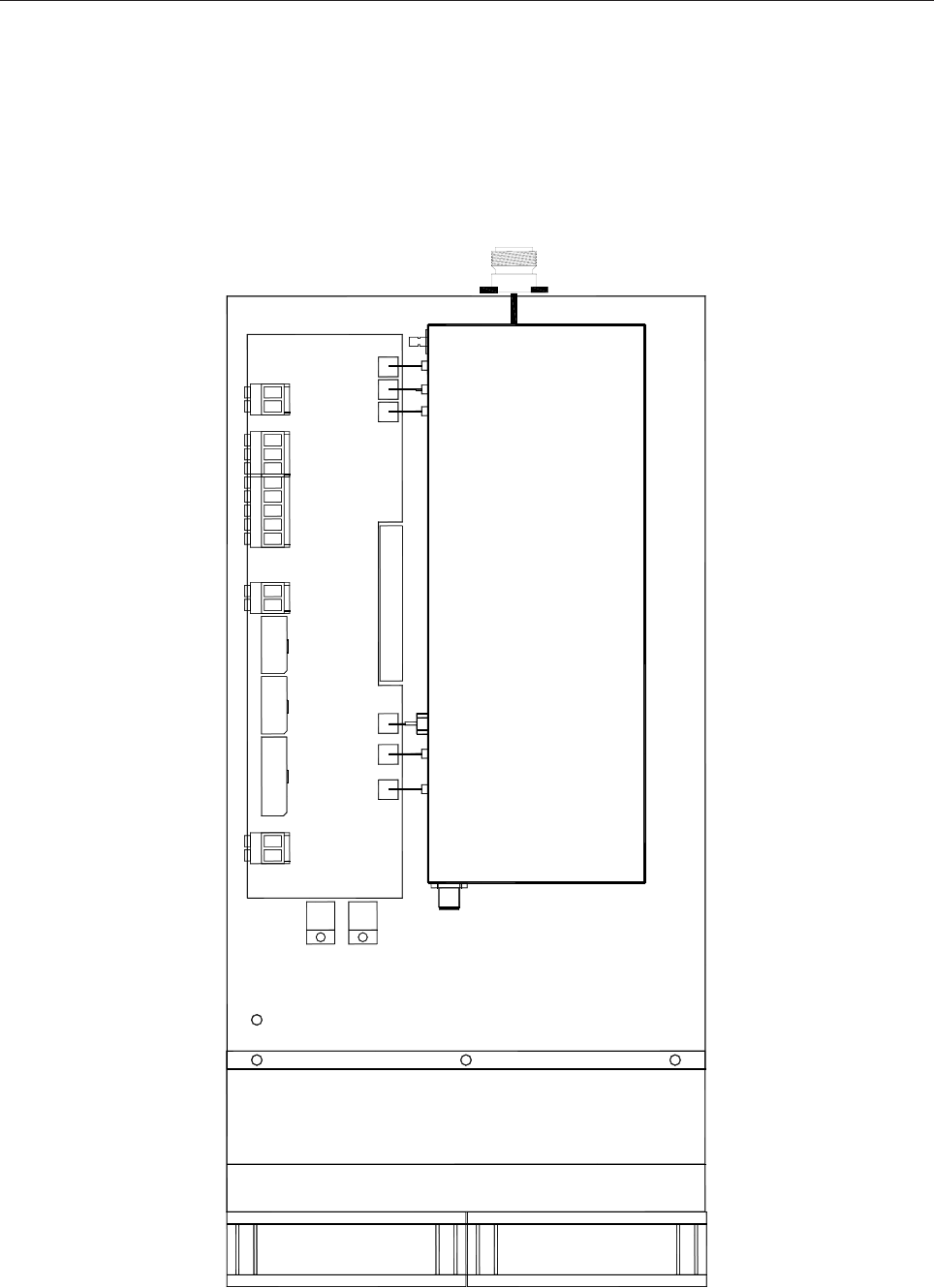
85
MTF0118A Component layout
SCH0388B
J1
J2
+5V
REF
RF MONITOR
FWD
MTF0118A
RF OUT
GND
RF AMPLIFIER MODULE
J5
GATE
TP7
+28V
TP4
CTRL
TP8
J9
J8
J7
J6
RF IN
CTRL
GATE
+28V
FWD
TP1
TP3
+5V
REF
TP2
POWER SUPPLY BOARD
J4
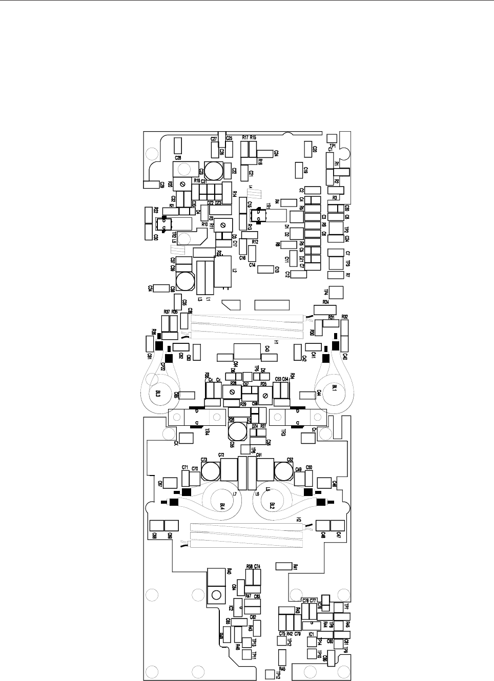
86
SCH0436AR0 Component layout

87
SCH0436AR0 COMPONENT LIST
Part Name/Number Description Qty. Comps. Page 1/2
CC 100nF-S 01065C 01065C Y5V 1206 CAPACITOR 11 C9, C17, C23, C33, C39, C56, C58, C77, C80,
C82, C85
CC 100pF-S 01092 01092 SMD 1206 CAPACITOR 2 C50, C54
CC 10pF-S 01086 01086 SMD 1206 CAPACITOR 2 C14, C29
CC 1206 N. M. N. M. SMD 1206 CAPACITOR 4 C20, C28, C34-35
CC 1nF 01041 01041 CERAMIC CAPACITOR 1 C45
CC 1nF-S 01096 01096 SMD 1206 CAPACITOR 26 C1-3, C6-7, C10-11, C15-16, C18, C21, C24,
C25, C30, C32, C36-37, C41, C49, C53, C78,
C79, C81, C83-84, C86
CC 1uF 100V 01077A CERAMIC CAPACITOR 1 C51
CC 2p2F-S 01081B 01081B SMD 1206 CAPACITOR 3 C12-13, C27
CC 33pF-S 1023A 1023A SMD 1206 CAPACITOR 1 C44
CC 47pF-S 01100 01100 SMD 1206 CAPACITOR 2 C40, C43
CC 4p7F-S 01083 01083 SMD 1206 CAPACITOR 2 C19, C26
CC 68pF-S 01027A 01027A SMD 1206 CAPACITOR 1 C42
CC 6p8F-S 01084 01084 SMD 1206 CAPACITOR 2 C74-75
CE 10uF16V-S 01626B TANT. ELET. SMD CAP. 6 C4-5, C8, C31, C57, C76
CE 10uF50V-S 01779A 01779A ELET. SMD CAPACITOR 4 C22, C38, C52, C55
CP 10pF-S 01117 CHIP CHB 1 C47
CP 1nF-S 01145 CHIP CHB 1 C48
CP 33pF-S 01127 CHIP CHB 1 C46
D 1N4148-S 03002 03002 SMD DIODE 3 D3-5
D HSMP3814 03202 SMD DIODE 2 D1-2
DZ 3V9-S 03134 SMD ZENER DIODE 4 DZ2-5
DZ 5V1-S 03128 03128 SMD ZENER DIODE 1 DZ1
IC AD8361 04899 04899 SMD INTEG CIRCUIT 2 IC1-2
IND 0u6H INDUCTOR 2 L4-5
IND CBD8 05072 05072 INDUCTOR 3 L1, L3, L6
IND VK200 05013 05013 INDUCTOR 1 L2
R 0R33-1W-S 00380 RES 1W 5% SMD 2512 2 R14, R23
R 100R-1/2W 00139 00139 RES 1/2W 5% 1 R33
R 100R-S 00029A 00029A RES 1/4W 5% SMD 1206 3 R44, R46, R48
R 10K-1%-S 00053B 00053B RES 1/4W 1% SMD 1206 2 R10, R19
R 10R-S 00017A 00017A RES 1/4W 5% SMD 1206 1 R34
R 1206 N. M. N. M. RES 1/4W 5% SMD 1206 2 R45, R49
R 18R-S 00020A 00020A RES 1/4W 5% SMD 1206 3 R2, R16, R31
R 270R-S 00034A 00034A RES 1/4W5% SMD 1206 6 R1, R3, R15, R17, R30, R32
R 2K7-1%-S 00046B RES 1/4W 1% SMD 1206 2 R5-6
R 330R-S 00035B 00035B RES 1/4W 5% SMD 1206 3 R9, R13, R22
R 39R-S 00024A 00024A RES 1/4W 5% SMD 1206 2 R12, R21
R 3K3-1W-S 00400 RES 1W 5% SMD 2512 2 R18, R26
R 3K9-1%-S 00048B 00048B RES 1/4W 1% SMD 1206 1 R7
R 47R-S 00025A 00025A RES 1/4W 5% SMD 1206 2 R42, R58

88
Part Name/Number Description Qty. Comps. Page 2/2
R 560R-1%-S 00038B 00038B RES 1/4W 1% SMD 1206 2 R4, R8
R 56K-S 00062A RES 1/4W 5% SMD 1206 1 R27
R 68R-S 00027A 00027A RES 1/4W 5% SMD 1206 2 R41, R54
R 75R-1%-S 00221B 00221B RES 1/4W 1% SMD 1206 2 R43, R47
RV 50K-S-H/S 00797 00797 SMD VARIABLE RESISTOR 3 R11, R20, R25
TR BLF1043-S 03469 LDMOS TRANSISTOR 2 TR1-2
TR MRF373A-S 04031A LDMOS TRANSISTOR 1 TR3

89
5W VHF-I RMS AMPLIFIER MODULE MTF0125AR0
DESCRIPTION
The MTF0125A is the final stage of the 5W VHF-I RMS of the transmitter, based on MOS technology. It includes
the final stage itself (SCH0320A), its cooling heatsink, and an interface board (SCH0388B) which allows to control
the forward power, the reflect power, the Gain and the temperature. The final amplifier is provided with a GATE
control to inhibit the power output, a circuit to monitor the output and the needed circuits to read the output forward
and reflected power. The power reading is an RMS measurement.
TECHNICAL CHARACTERISTICS
Output Power 5W RMS
Frequency Range 55 - 90MHz
Gain 32 - 34dB ±0.5
Power Supply 28V ±2%
Total Quiescent Current (cold) 2.6A
Output Impedance 50Ω
Input Impedance 50Ω
Input Return Loss >15dB
MTF0125A COMPONENT LIST
Part Name Code Description Qty
00041B 1kΩ 1206 SMD RESISTOR 1
00664 LM35DT THERMAL SENSOR 1
01041 1nF 50V CERAMIC CAPACITOR 1
01096 1nF MULTITURN CHIP CAPACITOR 1
01400 BYPASSING CAPACITOR 2
01403 BYPASSING CAPACITOR 5
02238 N FLANGE FEMALE CONNECTOR 1
02502 SMA SOCKET 1
02515 SMB SCREW 1
03202 HSMP 3814-TRIG DIODE 1
03469 BLF 1043 TRANSISTOR 1
03985 BLF 245 TRANSISTOR 1
05013 VK 200 1
08502 RG 316 50Ω CABLE 0.10
DET1026 DET1026R0 MECHANICAL DETAIL 1
DET1492R0P DET1492R0 HEAT SINK MODULE 1
SCA0091 SCA0091R0 COVER 1
SCA0140R0B SCA0140R0 AMPLIFIER MODULE BOX 1
SCH0320AR0 VHF AMPLIFIER MODULE 1
SCH0388BR1 POWER SUPPLY INTERFACE BOARD 1
V0771 3x5 MALE/FEMALE SPACER 4
TRANSISTOR NAME BIAS CURRENT
TR1 Pre-Driver BLF1043 0.4A
TR2 Driver BLF1043 0.6A
TR3 Output Stage MRF373 1.5A

90
MTF0125A Component layout
J8
J7
J6
RF IN
CTRL
GATE
+28V
FWD
TP1
TP3
+5V
REF
TP2
POWER SUPPLY BOARD
J4
SCH0388B
J1
J2
+5V
REF
RF MONITOR
FWD
MTF0125A
RF OUT
GND
RF AMPLIFIER MODULE
J5
GATE
TP7
+28V
TP4
CTRL
TP8
J9
91
SCH0320AR0 VHF-I Amplifier Board Component layout

92
SCH0320AR0 COMPONENT LIST
Part Name/Number Description Qty. Comps.
CC 100nF-S 01065C 01065C Y5V 1206 CAPACITOR 3 C4, C21, C23
CC 10nF 01053 01053 CERAMIC CAPACITOR 1 C22
CC 1206 N. M. N. M. SMD 1206 CAPACITOR 2 C28, C32
CC 1nF-S 01096 01096 SMD 1206 CAPACITOR 10 C2, C8-9, C18-20, C26-27, C30-31
CC 4p7F1%-S 01083A 01083A SMD 1206 CAPACITOR 1 C11
CE 10uF63V 01779 01779 ELET. CAPACITOR 5 C5-7, C29, C33
CP 100pF-S 01135 CHIP CHB 1 C12
CP 180pF-S 01137A CHIP CHB 1 C17
CP 1nF-S 01145 CHIP CHB 2 C14, C25
CP 22pF-S 01125 CHIP CHB 1 C24
CP 51pF-S 01129 CHIP CHB 1 C16
CP 68pF-S 01131 CHIP CHB 2 C13, C15
CV 3-10pF-S 01475 01475 VARIABLE CAPACITOR 3 C1, C3, C10
D 1N4148-S 03002 03002 SMD DIODE 2 D1-2
D BAT54S 03199 SMD SCHOTTKY DIODE 2 D3-4
DZ 3V9-S 03134 SMD ZENER DIODE 4 DZ1-4
IND CBD8 05072 05072 INDUCTOR 2 L12-13
IND RFC-G INDUCTOR 6 L1-6
IND VK200 05013 05013 INDUCTOR 5 L7-11
R 0R68-1W-S 00381 RES 1W 5% SMD 2512 1 R9
R 100R-S 00029A 00029A RES 1/4W 5% SMD 1206 2 R16-17
R 10K 0053 0053 RES 1/4W 5% 1 R19
R 18R-S 00020A 00020A RES 1/4W 5% SMD 1206 1 R3
R 22K-S 00057A 00057A RES 1/4W 5% SMD 1206 2 R6, R12
R 270R-1/2W 00144 RES 1/2W 5% 1 R15
R 270R-S 00034A 00034A RES 1/4W5% SMD 1206 2 R1-2
R 330R-S 00035B 00035B RES 1/4W 5% SMD 1206 1 R10
R 33K-S 00059A 00059A RES 1/4W 5% SMD 1206 1 R13
R 39R-S 00024A 00024A RES 1/4W 5% SMD 1206 1 R4
R 47K-S 00061A 00061A RES 1/4W 5% SMD 1206 1 R5
R 4K7-1W-S 00401 RES 1W 5% SMD 2512 2 R8, R14
R 56R 0026 0026 RES 1/4W 5% 1 R18
RV 50K-S-H/S 00797 00797 SMD VARIABLE RESISTOR 2 R7, R11
TR BLF1043-S 03469 LDMOS TRANSISTOR 1 TR1
TR BLF245-S 03985 LDMOS TRANSISTOR 1 TR2
93
SCH0388BR1 Component layout
POWER SUPPLY INTERFACE BOARD SCH0388BR1

94
SCH0388BR1 COMPONENT LIST
Part Name/Number Description Qty. Comps.
CC 100nF-S 01065C 01065C Y5V 1206 CAPACITOR 17 C1, C4-6, C10-17, C19, C21-24
CC 1206 N. M. N. M. SMD 1206 CAPACITOR 1 C7
CE 100uF16V-S 01792A 01792A ELET. SMD CAPACITOR 1 C9
CE 10uF35V-S 01778A 01778A ELET. SMD CAPACITOR 2 C18, C25
CE 10uF50V-S 01779A 01779A ELET. SMD CAPACITOR 1 C20
CE 220uF 35V-S 01798A ELET. SMD CAPACITOR 1 C8
CE 220uF50V LOW ESR 01799A ELET. SMD CAPACITOR 2 C2-3
D 1N4148-S 03002 03002 SMD DIODE 1 D2
D 50WQ06FN 03019A SMD DIODE SCH. 5.5A 1 D1
DL KA-3528SGC 03057 03057 GREEN SMD LED DIODE 3 DL1-3
FUSE 2A-PCB 7543 7543 FUSE HOLDER+FUSE 5x2 1 F1
IC 7805 04315 04315 VOLTAGE REGULATOR 1 IC2
IC INA168 04600A SMD INTEG CIRCUIT 1 IC3
IC LM2599T-ADJ INTEG CIRCUIT 1 IC1
IC LM317 04340 04340 INTEG CIRCUIT 1 IC6
IC LM35DT 00664 00664 INTEG CIRCUIT 1 IC7
IC LMC6484-S 04634 SMD INTEG CIRCUIT 1 IC4
IC TC7662BCOA 04758A 04758A SMD INTEG CIRCUIT 1 IC5
IND 2u2H-S 05020A 05020A INDUCTOR 1 L3
IND CBD8 05072 05072 INDUCTOR 1 L4
IND MS85 10uH-S 04948 INDUCTOR 2.7A 1 L2
IND T100uH-5A 05062A TOROIDAL-STORAGE 1 L1
J CON HD515V/05-3PVE 02893 + 02894 PANDUIT PCB 1 J2
J CON HD515V/05-5PVE PANDUIT PCB CONNECTOR 1 J4
J FC-10P 02697-02699 02697+02699 PCB CONNEC. POL 3 J3, J6-7
J FC-16P 02701-02700 02701+02700 PCB CONNEC. POL 1 J8
JU JUMP2 02739-02742 02739+02742 MALE PAN2 4 JP1-4
R 0R02 00356 RES 20W 1% 1 R8
R 100R-1%-S 00029D 00029D RES 1/4W 1% SMD 1206 6 R9, R11, R16, R20-21, R29
R 10K-1%-S 00053B 00053B RES 1/4W 1% SMD 1206 6 R12, R19, R22, R24-25, R27
R 1206 N. M. N. M. RES 1/4W 5% SMD 1206 1 R3
R 150K-S 00067A 00067A RES 1/4W 5% SMD 1206 1 R10
R 1K0-1%-S 00041B 00041B RES 1/4W 1% SMD 1206 2 R1, R5
R 220R-S 00033A 00033A RES 1/4W 5% SMD 1206 1 R26
R 2K7-S 00046A 00046A RES 1/4W 5% SMD 1206 1 R6
R 330R-S 00035B 00035B RES 1/4W 5% SMD 1206 1 R7
R 33K-1%-S 00059B 00059B RES 1/4W 1% SMD 1206 2 R18, R23
R 47K-1%-S 00061B 00061B RES 1/4W 1% SMD 1206 1 R14
R 560R-1%-S 00038B 00038B RES 1/4W 1% SMD 1206 1 R2
R 68K-1%-S 00063B 00063B RES 1/4W 1% SMD 1206 2 R13, R17
R 6K8-S 00051A 00051A RES 1/4W 5% SMD 1206 1 R28
R 8K2-1%-S 00052B 00052B RES 1/4W 1% SMD 1206 2 R4, R15
TR BC847 03456 03456 NPN SMD TRANSISTOR 1 TR1
95
SP-320-27/48 SWITCHING POWER SUPPLY E0064
MAIN FEATURES
- Universal AC input / Full range
- Built-in active PFC function, PF >0.95
- Protections: Short circuit / Over load / Over voltage / Over temp.
- Forced air cooling by built-in DC fan
- Built-in fan speed control
- Fixed switching frequency at 100kHz
MECHANICAL SPECIFICATION
Air flow
direction
215
32.5
50
25
4-M4 L=6mm
150
C
L
PIN N° ASSIGNMENT
1AC/L
2AC/N
3FG
4-5 DC OUTPUT -V
6-7 DC OUTPUT +V

96
TECHNICAL CHARACTERISTICS
MODEL SP-320-27 SP 320-48
OUTPUT
DC VOLTAGE 27V 48V
RATED CURRENT 11.7A 6.7A
CURRENT RANGE 0 ~ 11.7A 0 ~ 6.7A
RATED POWER 315.9W 321.6W
RIPPLE & NOISE (max.) Note 2 200mVp-p 240mVp-p
VOLTAGE ADJ. RANGE 26 ~ 31.5V 41 ~ 56V
VOLTAGE TOLERANCE Note 3 ± 1.0% ± 1.0%
LINE REGULATION ± 0.2% ± 0.2%
LOAD REGULATION ± 0.5% ± 0.5%
SETUP, RISE TIME 800ms, 50ms/230VAC 2500ms, 50ms/115VAC at full load
HOLD UP TIME (Typ.) 16ms/230VAC 124 ~ 370VDC
INPUT
VOLTAGE RANGE 88 ~ 264VAC 124 ~ 370VDC
FREQUENCY RANGE 47 ~ 63Hz
POWER FACTOR PF>0.95/230VAC PF>0.95/115VAC at full load
EFFICIENCY (Typ.) 88% 89%
AC CURRENT 5A/115VAC 2.5A/230VAC
INRUSH CURRENT (Max.) 20A/115VAC 40A/230VAC
LEAKAGE CURRENT <1mA/240VAC
PROTECTION
OVER LOAD
105 ~ 135% rated output power
Protection type: Hiccup mode, recovers automatically after fault condition is removed
OVER VOLTAGE
33.7 ~ 39.2V 57.6 ~ 67.2V
Protection type: Hiccup mode, recovers automatically after fault condition is removed
OVER TEMPERATURE
80°C ±5°C (70°C ±5°C 3.3V, 5V only) (TSW1: Detect on heat sink of power transistor)
Protection type: Shut down o/p voltage, recovers automatically after temperature goes down)
ENVIRONMENT
WORKING TEMP. -20 ~ +65°C (Refer to output load derating curve)
WORKING HUMIDITY 20 ~ 90% RH non-condensing
STORAGE TEMP., HUMIDITY -40 ~ +85°C, 10 ~ 95% RH
TEMP. COEFFICIENT ± 0.03%/°C (0 ~ 50°C)
VIBRATION 10 ~ 500Hz, 2G 10min./1cycle, period for 60min. each along X, Y, Z axes
SAFETY & EMC
(Note 4)
SAFETY STANDARDS UL60950-1, TUV EN60950-1 Approved
WITHSTAND VOLTAGE I/P-O/P:3KVAC I/P-FG:1.5KVAC O/P-FG:0.5KVAC
ISOLATION RESISTANCE I/P-O/P, I/P-FG, O/P-FG:100M Ohms/500VDC
EMI CONDUCTION & RADIATION Compliance to EN55022 (CISPR22) Class B
HARMONIC CURRENT Compliance to EN61000-3-2,-3
EMS IMMUNITY Compliance to EN61000-4-2,3,4,5,6,8,11; ENV50204, Light industry level, criteria A
OTHERS
MTBF 207K hrs min. MIL-HDBK-217F (25°C)
DIMENSION 215*115*50mm (L*W*H)
PACKING 1.1kg