Elettronika S r l TXUD1000A 1000 W ATSC Transmitter User Manual TXUD1000A Part 2

Elettronika S.r.l. 1000 W ATSC Transmitter TXUD1000A Part 2

Contents

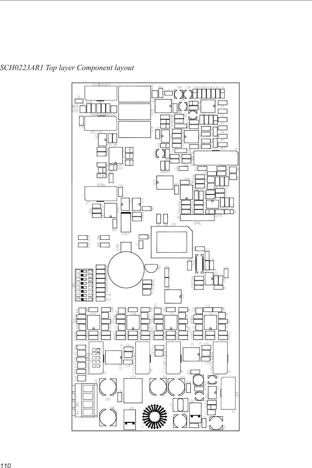
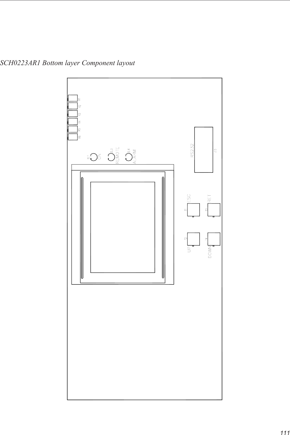
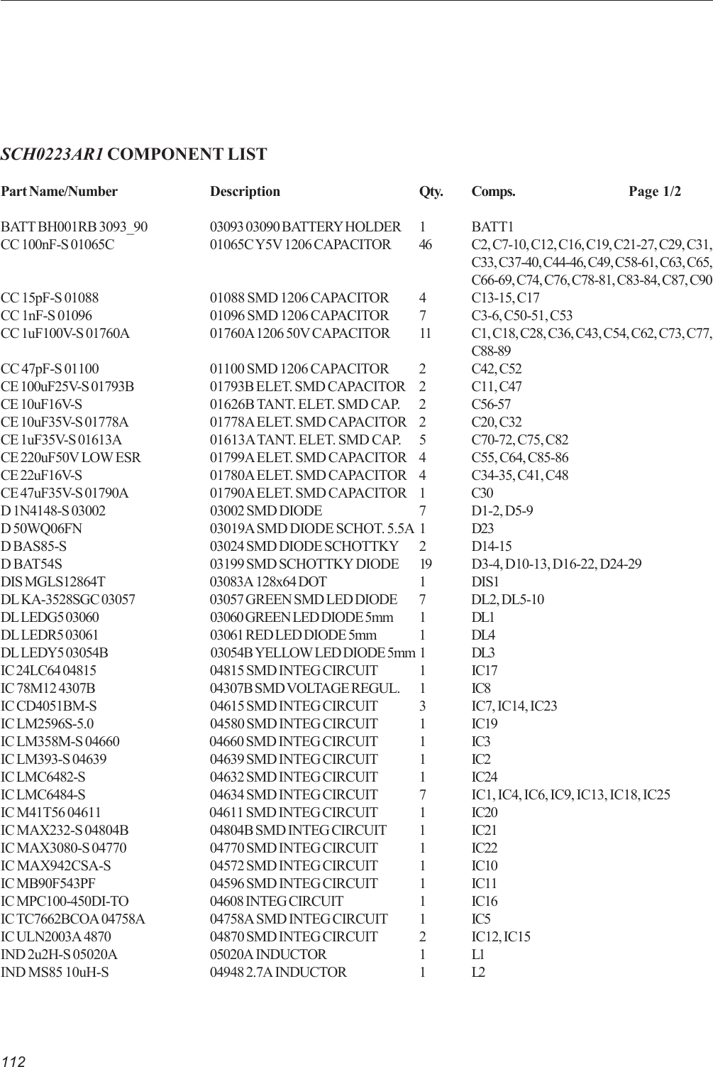
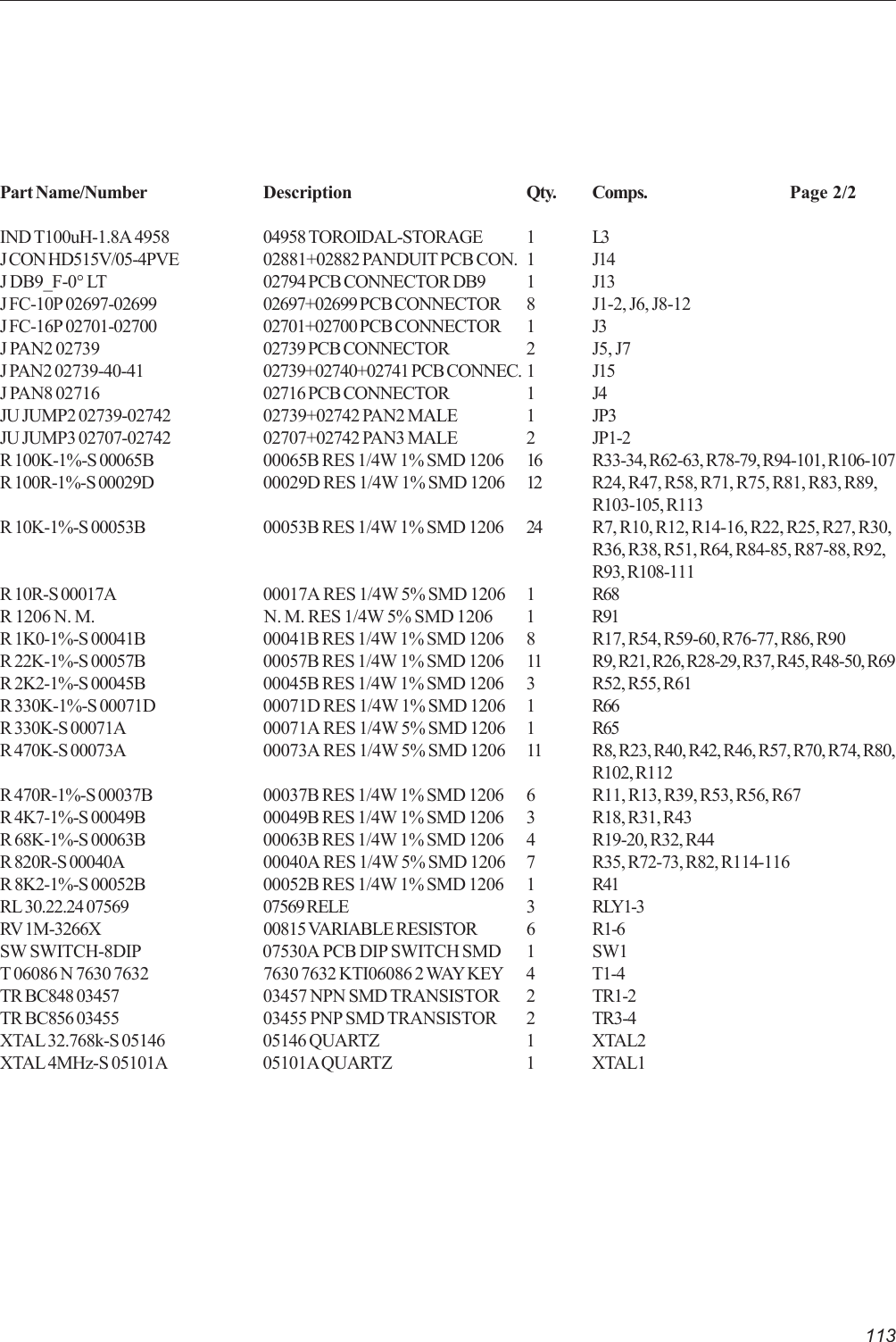
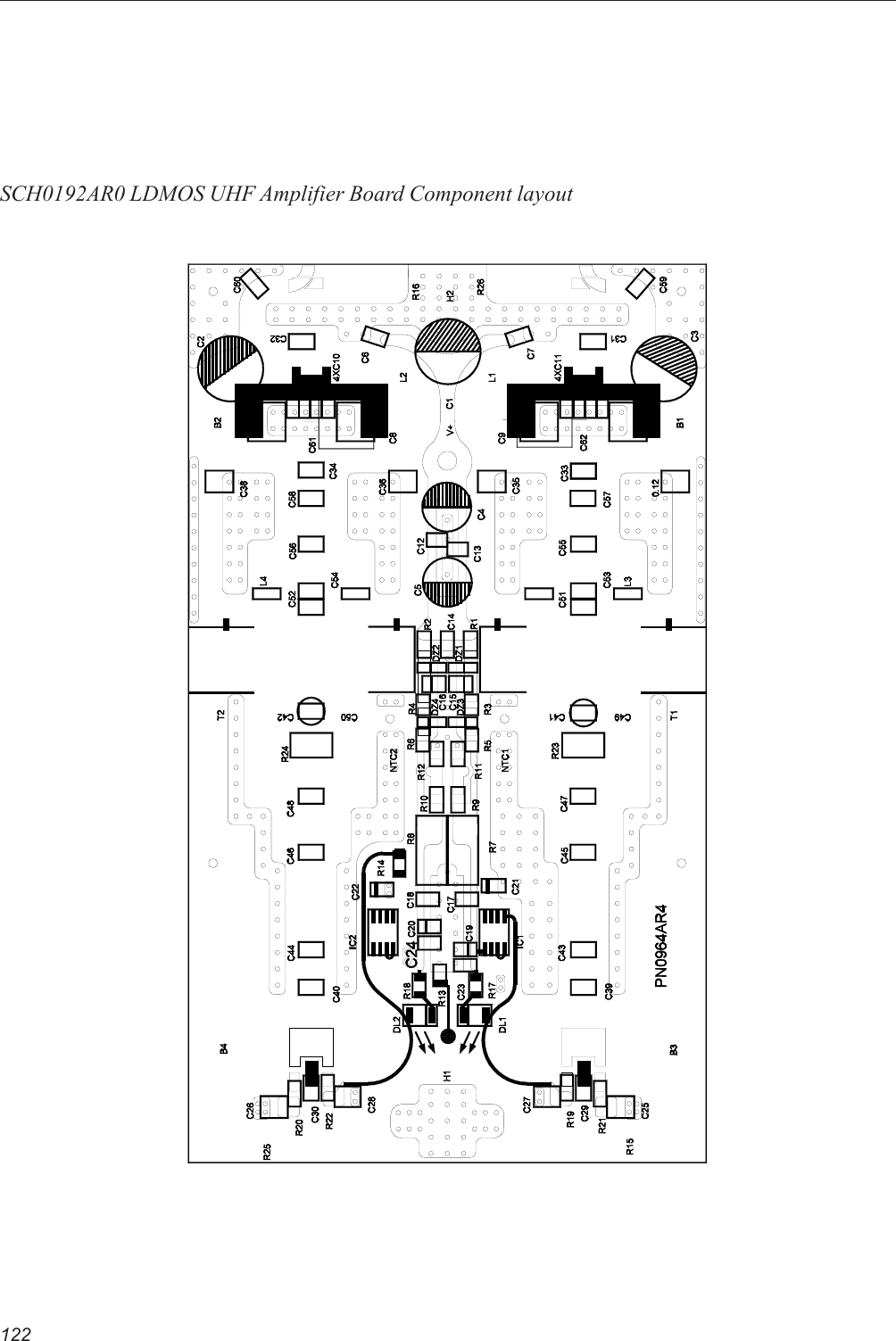
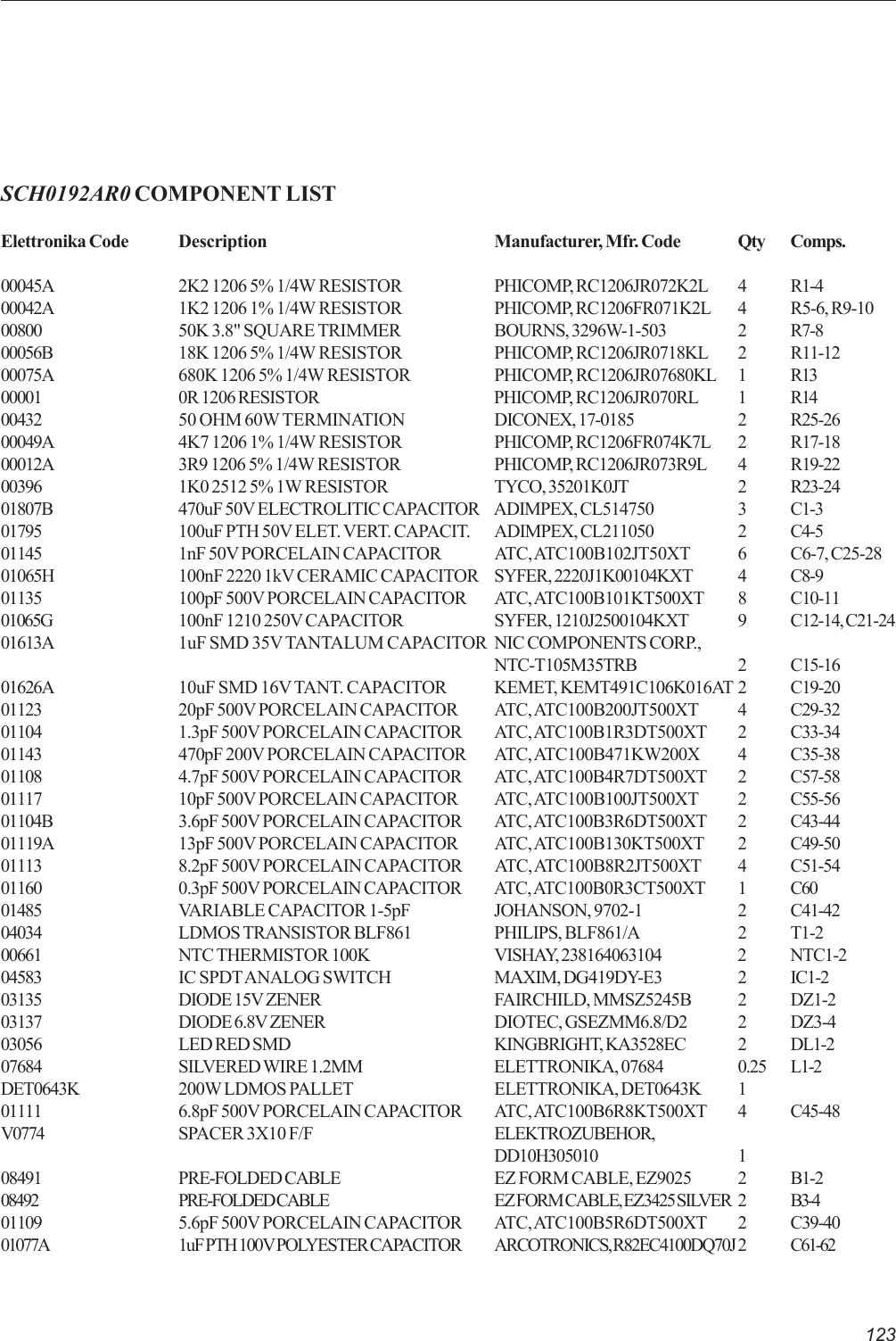
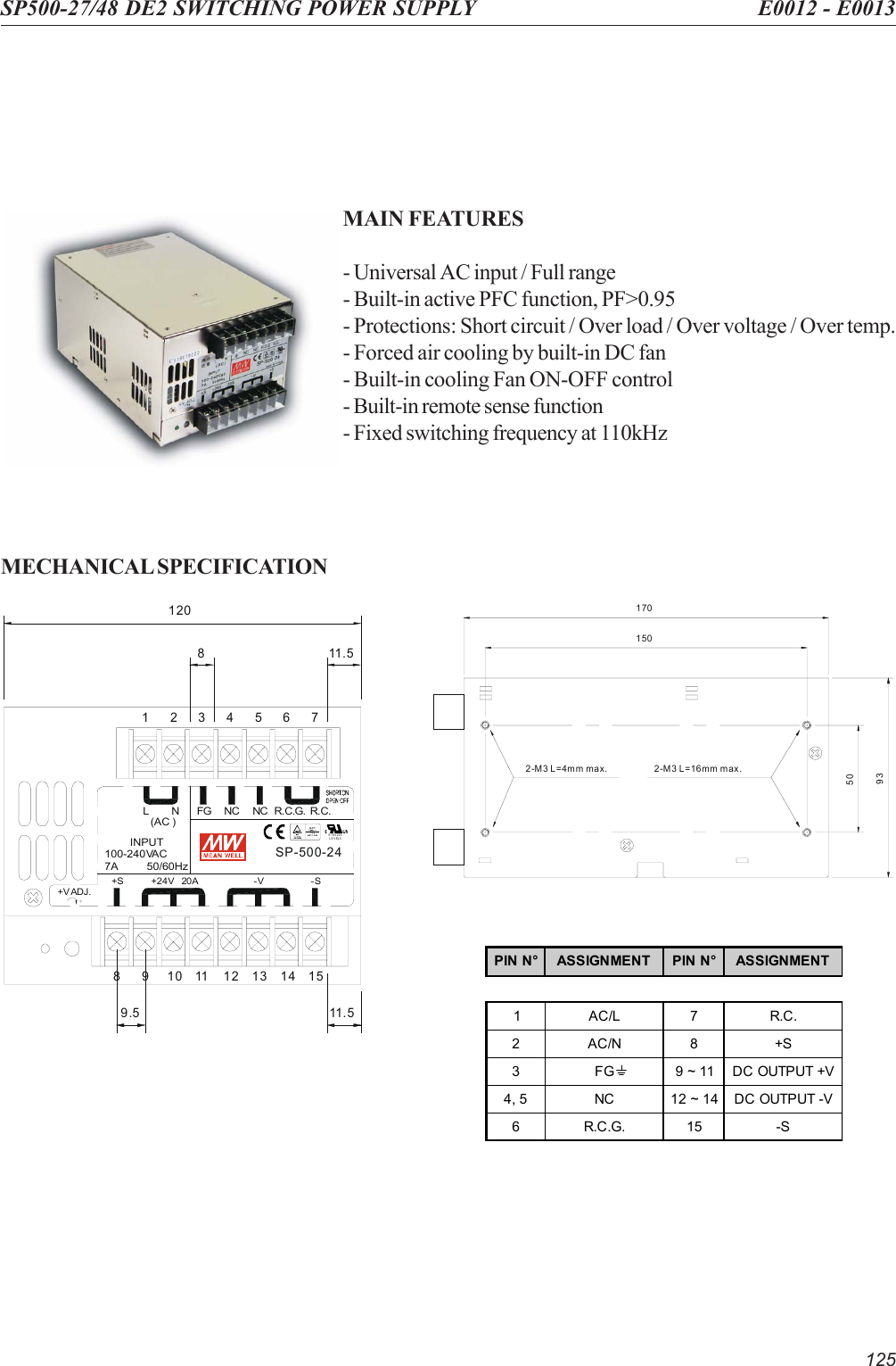
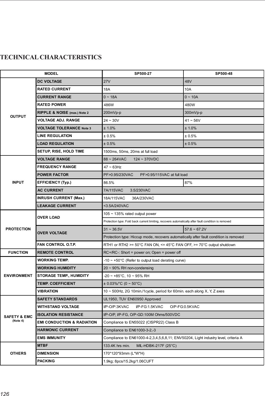
TXUD1000A User Manual Part 2

76LDMOS UHF SERIESMEDIUM POWER TV AMPLIFIERUser’s manual
77This page is intentionally blank
78Section 1 - InformationContents:1.1 Description1.2 Main Features1.3 Technical characteristics1.4 Front panel1.5 Rear panelRear connections
791.1 DESCRIPTIONThe amplifier belongs to the Medium Power Amplifier products family of Television Amplifiers fully in solidstate LDMOS technology.These TV Amplifiers operate in the UHF Band with Common amplification process (separate amplificationavailable) of the Video and Audio carriers. This Amplifier family has been designed to offer to the customerhigh performances, high reliability and greater simplicity in its operation and maintenance procedures.The Video and Audio signal processing is provided for all TV Standards and all types of Audio applications(Mono & Dual Sound - NICAM) together with the different colour systems such as PAL - NTSC - SECAM.Thanks to the amplitude and phase and non linearity pre-correction circuit, it is possible to cancel the distortionsin the output stage, thus cutting down the operating costs.Due to the common amplification design, the transmitter is easily upgradeable to any digital TV standard:DVB-T, DVB-H, DMB-T, ATSC. It is only necessary to replace the modulator and the RF output band passfilter, all the other components are used without any change.The cooling system is fully contained into the amplifier, and it is based on forced air flow. A powerful and verylow acoustic noise blower is used. A front panel air dust filter is available, sized in order to enable easyreplacement.The user interface is based on a graphics display, where all the parameters are showed. A detailed log ofevents and alarm help the maintenance of the system.The unit can be fully controlled in REMOTE mode via PC direct-link or via PSTN, GSM or Ethernet networksby means of Elettronika Remote Control System.The system can be easily upgraded with dual drive option.Besides, the transmitter can be easily integrated in a 1+1 or more complex N+1 redundancy configurations.1.2 MAIN FEATURES- LDMOS Technology;- Forced-air cooling system;- Analog and Digital input signal;- High efficiency;- Wired and serial remote control (RS232 or RS485);- All voltages and currents available on display;- Output filter included.MEDIUM POWER TV AMPLIFIERSERIES
801.3 TECHNICAL CHARACTERISTICSRF SECTIONAnalog OperationFrequency Range ........................................................................................................................................................... UHFOutput Power (±0.5dB) ............................................................................................................................................... 1300WAmplification Class .......................................................................................................................................................... ABGain (±2dB) .................................................................................................................................................................... 28dBTechnology ............................................................................................................................................. Solid State LDMOSRF Input Connector ................................................................................................................................................ N FemaleImpedance ....................................................................................................................................................................... 50ΩRF Output Connector (Amplifier / Rack) ........................................................................................... 7/16” Female / EIA 7/8”Impedance ....................................................................................................................................................................... 50ΩDigital OperationFrequency Range ........................................................................................................................................................... UHFDigital Output Power (DVB-T) .............................................................................................................................300W RMSDigital Output Power (ATSC) ...............................................................................................................................500W RMSDVB-T Modes ......................................................................................................... All the modes listed in ETSI EN 300 744DVB-T MER ....................................................................................................................................................... > 33dB RMSDVB-T Shoulders Attenuation (After non-critical mask cavity filter) ................................................................ > 40dB RMSDVB-T Output Spectrum ............................................................................................................. Compliant ETSI EN 300 744ATSC Symbol Rate ...................................................................................... 10.76MBaud/s (Compliant to ATSC Doc. A/53)ATSC SNR ......................................................................................................................................................... > 27dB RMSATSC Shoulders Attenuation (After simple mask cavity filter ref. total output power) ..................................... > 46dB RMSATSC Output Spectrum ......................................................................................................... Compliant to ATSC Doc. A/64REMOTE CONTROL SECTIONParallel Interface ........................................................................................................................... ON/OFF, Alarms, InterlockSerial Interface ............................................................................................................................. RS232 or RS485 SelectableMETERINGOutput Forward Power (Peak or RMS)Output Reflected Power (Peak or RMS)Unbalance PowerHeat sink TemperatureInput Power (Peak or RMS)RF Modules CurrentPower Supply VoltageWorking TimerINDICATIONSCooling Blower Working (With icon on front display)Transmitter Interlock (With icon on front display)Alarm (With red LED on front panel)Transmitter ON/OFF (With green LED on front panel)Remote ON/OFF (With orange LED on front panel)
81PROTECTIONSOutput Forward PowerOutput Reflected PowerUnbalance PowerRF Modules CurrentPower Supply VoltagePROTECTIONSForward Power (Analogue) ......................................................................................................................................... 1500WReflected Power (Analogue) .........................................................................................................................................150WForward Power (DVB-T) ................................................................................................................................................400WReflected Power (DVB-T) ............................................................................................................................................... 40WForward Power (ATSC) .................................................................................................................................................600WReflected Power (ATSC) ................................................................................................................................................ 60WUnbalance (Analogue) ..................................................................................................................................................300WUnbalance (DVB-T) .......................................................................................................................................................100WUnbalance (ATSC) ........................................................................................................................................................150WTemperature ................................................................................................................................................................... 75°CIDC ....................................................................................................................................................................................................................................................................................................................... 18AVDC ....................................................................................................................................................................................................................................................................... Min 10V - Max 33.5VGENERALPower Supply Voltage ............................................................................................................................................. 90 - 260VPower Supply Frequency ........................................................................................................................................ 50 - 60HzPower Factor .................................................................................................................................................................> 0.98Analog Power Consumption (Black) ......................................................................................................................... 3.45kVADigital Power Consumption (DVB-T) .......................................................................................................................... 2.2kVADigital Power Consumption (ATSC) ........................................................................................................................... 2.5kVAHousing (Amplifier / Rack) ...................................................................................................................................... 6U / 20UWeight (Amplifier / Rack)................................................................................................................................... 63kg / 175kgAirflow ............................................................................................................................................From 330m3/h to 500m3/hTemperature ..................................................................................................................................................... -5°C to +45°COptions- Non critical mask, DVB-T, Output filter- Critical mask, DVB-T, Output filter- Stringent emission mask, ATSC, Output filter
821.4 FRONT PANEL2 3 511. Function keys2. LCD Graphic Display3. Status LEDs4. RS232 Socket5. RF Monitor Connector6. Main Switch64RS232 for connectionto PC with ERCoS softwareand for firmware upgradePin 2: TXPin 3: RXPin 5: GND
83FUSEFUSEFUSE11.6 REAR PANEL1. Breaker2. AC 220V OUT Socket3. AC 400V IN Socket41. FAN 3.15A Fuse42. CONTROL BOARD 1A Fuse43. EXCITER 4/8A Fuse5. RF IN Connector6. RS485 Socket7. EXCITER Socket8. TELEMEASURES Socket9. RF OUT Connector62 35 97 8Wired Telemeasures connectorPin 1: FWD power (Analog out)Pin 2: REF power (Analog out)Pin 3: Temperature (Digital out)Pin 4: Interlock (Digital in)Pin 5: GNDPin 6-7: Free contact (Digital out)Closed when AlarmPin 8: 0V=ON / 5V=Normal (Digital in)Pin 9: 0V=OFF / 5V=Normal (Digital in)EXCITER for connectionto Driver ModulePin 1: GNDPin 2: 0V=Normal / 5V=AGC Alarm(Digital out)Pin 3: 0V=Normal / 5V=AGC Alarm(Digital out)Pin 8: FWD power (Analog out)Pin 9: REF power (Analog out)RS485 for connectionto RCU or Amplifier ControlPin 2: RX- Pin 5: GNDPin 3: RX+ Pin 7: TX-Pin 4: +5V Pin 8: TX+424341
84Section 2 - InstallationContents:2.1 Operating environment2.2 First installation2.3 Connection with VEGA Transmitter2.4 Stand-alone Amplifier configuration in Dual Drive version2.5 Slave multi-Amplifier configuration with Amplifier Control2.6 Stand-alone Amplifier configuration with Elettronika RCU2.7 Stand-alone Amplifier configuration with direct PC connection
852.1 OPERATING ENVIRONMENTYou can install the equipment in a standard component rack or on a suitable surface such as a bench or desk.In any case, the area should be as clean and well-ventilated as possible. Do not locate the equipment directlyabove a hot piece of device. The upper lid can be dismounted to allow an easy internal access. The equipmentis designed with a modular design, that is each circuit is realized inside different modules or boards. Allinterconnections between modules are made by means of connectable cables which allow an easy and quickmaintenance of demaged modules.2.2 FIRST INSTALLATIONCorrect installation of the equipment is important for maximum performance and reliability. Antenna and earthconnections must be installed with the greatest care. The equipment adjustment isn’t need, because the unit iscompletely adjusted by our technical staff.1. Connect Power Supply cable of the Exciter to the Auxiliary Socket on the rear panel of the Amplifier;2. connect the Power Supply cable of the Amplifier to the electric network (230VAC Monophase or 400VAC     Threephase); if present the Isolator Transformer, the Amplifier is provided with cable and plug;3. connect the RF OUT Exciter cable to the RF IN connector on the rear panel of the Amplifier;4. connect the Antenna cable to the RF OUT connector on the rear panel of the Amplifier.AGCBREAKERAC 200V OUTRF IN RS485 TELEMEASURESAC 400V INRF OUTTo  ANT E N N ATo ELECTRIC NETWORKTo  EXC I T E RRF INPUT
86When the equipment is put within a combined system it is directly connected to the input splitting and outputcombining systems.Before fully powering the equipment, check that the output connections of the coaxial cable to the antennasystem are working.In order to this it is possible to check the indication of the Reflected Power at low power levels. Only if theSWR indication on the display is 0, the output power can be slowly increased. At maximum output power,some watts might be shown as Reflected Power.2.3 CONNECTION WITH VEGA TV TRANSMITTERAGC128584TV AMPLIFIER VEGABREAKERAC 200V OUTRS485 TELEMEASURESAC 400V INRF OUTRF INTo ELECTRIC NETWORKTo ANTEN NA
872.4 STAND-ALONE AMPLIFIER CONFIGURATION IN DUAL DRIVE VERSIONOUTMAINVIDEOOUTAUXAUXMAINGNDLEFTOUTAUXLEFTMAINLEFTOUTINRIGHTOUTAUXRIGHTMAINOUTRIGHTININAUXMAININ19kHzOUT DIRE CTREMO TEINRF AUX IN RF OUT RF MAIN INAUX CTRLRS232 /48 5REMOTEMAIN CTRLBREAKERAC 200V OUTAC 400V INRF OUTAGCRS485 TELEMEASURESRF INTo AN TENNA
882.5 SLAVE MULTI-AMPLIFIER CONFIGURATION WITH AMPLIFIER CONTROLBREAKERAC 200V OUTAC 400V INRF OUTAGCRS485 TELEMEASURES235235AMPLIF IER CONTROL AMPLIFIERRF INTo COMBINER7878From SPLITTER
892.7 STAND-ALONE AMPLIFIER CONFIGURATION WITH DIRECT PC CONNECTION2.6 STAND-ALONE AMPLIFIER CONFIGURATION WITH ELETTRONIKA RCUSERIAL PORTBREAKERAC 200V OUTAC 400V INRF OUTAGCRS485 TELEMEASURESRF IN
90Section 3 - OperationContents:3.1 Operation3.2 Display3.3 Menus3.4 Firmware upgrade
913.1 OPERATIONAt startup, after initial image, the display shows the main screen with the RF powers as below:The user may turn on and off the amplifier by means of the switch on the front panel. The control board turnson all the power supplies, the exciter (if any), and internal cooling fans. While the amplifier is working, themicro-controller monitors continuously the most important parameters: power supply voltages, absorbedcurrents, high power zone temperature, forward and reflected powers, unbalances (if any). Each measure isassociated to a maximum threshold beyond which the amplifier is immediately put in protection status byturning off one or more power supply, depending on the failed block. In order to prevent a temporary problemto trigger a definitive protection status, the failed block is turned on again, after some seconds, for up to fivetimes. If it goes beyond the protection threshold for more than five times, it is declared as FAILED and it willno longer be turned on. In this case, the amplifier will have to be turned off manually by means of the switch onthe front panel, then turned on again after performing the needed maintenance.On the front panel there are also three LEDs labelled ON, REMOTE and ALARM. Their meanings areexplained in Table 1.Table 1: Meanings of the three LEDs on the front panel1 Screenshots in this manual are indicative, so they can be different from those on your equipment.LED COLOUR MEANING MEANING WHEN BLINKINGON Green The amplifier is onThe amplifier has been turned onlocally but it has been turned off byremoteREMOTE Yellow Remote control isenabled It never b li nksALARM Red An alarm is present It never blinks
923.2 DISPLAYThe Control Board is provided with a modern pixels graphic display with blue background. Normally italways shows a title bar (on the top line) and a status bar (on the bottom line). The ‘Title bar’, shows the nameof the amplifier (TV Amplifier) and the current time. If the amplifier is a single unit coupled externally with otherunits in a high power transmitter, the title bar shows the amplifier number (slave address) too.The ‘Status bar’ indicates the forward and reflected powers and the temperature. It also contains two symbolsfor the interlock (lock) and the alarm (bell).The bell symbol is continuously displayed in case of alarm. It blinks if there has been an alarm which has endedbut has not yet been seen by the user. It stops blinking once the Log has been checked. The interlock symbolis displayed only when this function is enabled. It may be either a close lock, when there is no alarm (interlockchain closed) or an open lock in case of alarm (interlock chain open).Since the status bar is always showed on the display, regardless of the screen, the user may monitor at anytime the most important parameters and the presence of alarms while moving between different screens.3.3 MENUThe user may see or modify locally some configuration parameters using the four buttons on the front panel.All screens areorganized in a hierarchical menus and the user may move between them in a simple and intuitiveway. To see the menu it’s sufficient to press the ESC key.
93RF PowersThis is the main screen showing the RF powers of the amplifier: forward power, reflectedpower, unbalances, if any. For forward power a level bar is displayed. See an example inFigure 1.Power SupplyThis screen shows all the signals coming from two power supply. To check the next(previous) power supply press the UP (DOWN) key. For each power supply, the voltage,the absorbed current and the status (ON or OFF) are shown.The display only shows three items at a time: all the items can be scrolled by the UP and DOWN arrow keys.Any item can be chosen by selecting it and pressing the RET key. Menu  entries  with  an  arrow  on  the  right open sub-menus when chosen. Thus there is a hierarchical structure as below. To go back from a sub-menuto the previous menu, press the ESC key. If the ESC key is pressed in the main menu, the RF powers screenis accessed.Hierarchical menu structure
94Log/AlarmsThe control board is provided with an external EEPROM and a clock. Any alarm orswitching event with the time at which it occurred is saved in the EEPROM. The Log/Alarms sub-menu allows to manage this log.It is possible to see the events stored in the log by selecting Log/Alarms J View Log/Alarms. All events can be scrolled by pressing the UP and DOWN keys. For example,the event shown in Figure 7 is the turning on of the amplifier by means of the local switch.For every event/alarm a short description and the date and time at which it occurred isdisplayed.In case of alarm, the value of the measure which caused the alarm is saved into the log. Incase of alarm still existing after five turning-on attempts, the parameter is marked asFAILED. The table below is the list of all the events which can be logged.EVENT DESCRIPTIONLocal ON Amplifier turned on by means of the local switchLocal OFF Amplifier turned off by means of the local switchRemote ON Amplifier turned on remotelyRemote OFF Amplifier turned off remotelyInterlock open Interlock chain openInterlock closed Interlock chain closedPower Supply ON Power supply onFwd Pwr xxxxW Alarm for forward powerRef Pwr xxxxW Alarm for reflected powerUnbY xxxxW Unbalancing alarmV1 xx.xV Power supply voltage alarmI1 xx.xA Power supply current alarmThe log may be completely deleted by selecting Log/Alarms J Clear Log/Alarms.Amplifier can store in the log details about alarms and generic events. You can change thisbehaviour selecting Log/Alarms J Log/Mode menu item.Working TimerThe control board has a working timer which is always enabled while the amplifier is
95working (i. e. there is at least one power supply working). The menu entry WorkingTimer J View Timer allows to check the hours for which the timer has been enabled.Working Timer J Timer Reset resets the timer.ThresholdsThis is a screen showing the alarm threshold of each signals monitored by the controlboard. The list can be scrolled by means of the UP and DOWN keys.RMS/PeakThe control board can monitor both the RMS and peak powers, the first used in digitalsystems. The menu entry Settings J RMS/Peak allows to choose the power to be displayedand monitored. This menu is present only in certain amplifiers.Date/TimeThis screen allows to set the current date and time. The setting is changed by pressing thearrow keys, then pressing the RET key to move to the following value and eventuallysave the changes. To go back to the previous menu and discard any change made, pressthe ESC key.DisplayThe menu entry Settings J Display allows to change some settings of the display, suchhas back light, contrast and screensaver. The back light and the contrast are set by meansof the UP and DOWN arrow keys. The changes made are saved by pressing the RETkey or discarded pressing the ESC key.With Settings J Display J Screensaver you can set an interval time after which displaybacklight is turned off. When display backlight is off, press any key to switch it on.Frequency (only for some Amplifiers)The forward and reflected RF powers is measured by means of a directional coupler. Inorder to compensate for the effect due to the sampling made by the coupler, it is possibleto set the frequency by menu entry Settings J Frequency. The setting can be changed bypressing the arrow keys. The changes made are saved by pressing the RET key ordiscarded pressing the ESC key. Set the video carrier frequency.Slave AddressThe amplifier may be used either in stand-alone mode or as a slave of a master in a highpower multiple units transmitter. In the latter case an unique address for each amplifierhas to be specified, in order for all of them to communicate with the master on the sameRS485  bus. The  menu  entry  Settings J Slave Address allows to choose the stand-
96alone mode or set a slave address by means of the UP and DOWN arrow keys. Thechanges made are saved by pressing the RET key or discarded pressing the ESC key.RemoteThe amplifier may be controlled either locally, by means of the keys and display, orremotely. There are three possibilities for remote control:- using a direct serial connection between amplifier RS232 connector and a PC RS232;- using the remote control device manufactured by Elettronika S.r.l. (RCU), on the RS485;- using a general-purpose control system connected to telemeasures.You can enable / disable remote control choosing menu item Settings J Remote. Whenremote control is enabled, the yellow REMOTE LED on the front panel is lit.InterlockOne of the pins of the telemeasure connector, located on the rear panel, is used for theinterlock alarm. It is an input line which turns off the amplifier in case of alarm. Theinterlock check can be enabled or disabled using menu item Settings J Interlock. Whenit is enabled, the status bar shows the lock symbol, which is close if the interlock chain isclosed (no alarm) or open if it is open (alarm).Firmware ReleaseThe menu entry Settings J Firmware Release allows to display the firmware versionnumber and the hardware release of the amplifier.Serial NumberThe menu entry Settings J Serial Number allows to display the serial number of theapparatus.
973.4 FIRMWARE UPGRADEThe microcontroller is provided with a built-in Flash memory containing the firmware. The firmware can beupdated with a later version without removing the apparatus from the rack and/or replacing the chip.To upgrade it, connect a PC to the RS232 socket on the front panel of the apparatus by means of a cableDB9 male - DB9 female (pin-to-pin).Launch on the PC the EKAFlash application, select the serial port in use on the PC, choose the update file bypressing the “...” key and click on Download button.Eventually, turn off the amplifier from the main switch and then turn it on again. The upgrade of the firmwarebegins on the EKAFlash window. The figure below shows this window while a firmware is being updated.The EKAFlash window while updating a firmware
98Section 4 - DiagramContents:- APT144C AUTV/1500LD Cable diagrams- APT144C_APT144CM AUTV/1500LD Component list- Modules description
99FAN3.15AFANTP1TP2TP5TP3TP4TP6TP7TP10TP8TP9J3J7 J6J19TEMP+5VTEMP+5VJ21J2AUXILIARY SOCKET1A5A+24VGND1J14234 J15U21U19 U19U21U8U7U5U6U3U4U1U2U14U141243876587634512T1T2T3S1S2R1R2S3R3NNN7N6N8N3N2N4N5N1N10N9N 0N (EQUIPOTENTIAL)12435687T1N8N7T2N6T3S1N5N4S2S3N3R1N2R2N1R3R31R32R31R33R33N 0N10 N11N9 N91 N91FANL (EQUIPOTENTIAL)HANDLE ACTUATOR SW.SCH0221AAMPLIFIER INTRFACE BOARDSCH0223ACONTROL BOARD AND DISPLAYEXCITERRS485 TELEMEASURESJ9J10J11U9U10U11U11U10U9J4J29J11J391021102J7J5J69110 92 1J8102MAIN SWITCHSCH0288AINTERFACE BOARDJ3J6J1 J8 J12POWER SUPPLY #1POWER SUPPLY #2 POWER SUPPLY #4POWER SUPPLY #3RF MONITOR4V- L NV+ 5V-V+ LNV+ V- L NV+ NLV-SWITCHINGSP500-27/48POWER SUPPLY6ImCOMR.C.SP500-27/488V+ V- L NPOWER SUPPLYSWITCHINGVmImPOWER SUPPLYSP500-27/487R.C.VmImCOMSWITCHINGVmSWITCHINGPOWER SUPPLYSP500-27/48COMR.C.VmImCOMSP500-27/48SWITCHINGPOWER SUPPLYR.C.VmImCOMR.C.SP500-27/48POWER SUPPLYSP500-27/48V+L3V-V+ NV+ V-2V- NL1LNSWITCHINGCOMPOWER SUPPLYR.C.VmImCOMPOWER SUPPLYSWITCHINGSP500-27/48VmSWITCHINGImR.C.COMVmImR.C.ZNLNZLNZLLNJ3 J2 J1 J8PN1114AFANS CABLE BOARDJ1GDL NFJ2SCH0265AMAINS DISTRIBUTION BOARD
100ZNLNZLNZLLNJ3EXCITERRS485 TELEMEASURESHANDLE ACTUATOR SW.4V- LNV+ 5V-V+ L NV+ V- L NV+ NLV-SWITCHINGSP500-27/48POWER SUPPLY6ImCOMR.C.SP500-27/488V+ V- L NPOWER SUPPLYSWITCHINGVmImPOWER SUPPLYSP500-27/487R.C.VmImCOMSWITCHINGVmSWITCHINGPOWER SUPPLYSP500-27/48COMR.C.VmImCOMSP500-27/48SWITCHINGPOWER SUPPLYR.C.VmImCOMR.C.SP500-27/48POWER SUPPLYSP500-27/48V+L3V-V+ NV+ V-2V- NL1LNFAN3.15AFANSWITCHINGCOMPOWER SUPPLYR.C.VmImCOMPOWER SUPPLYSWITCHINGSP500-27/48VmSWITCHINGImR.C.COMVmImR.C.TP1TP2TP5TP3TP4TP6TP7TP10TP8TP9J3J7 J6J19TEMP+5VTEMP+5VJ21 J3J2J9J10J11AUXILIARY SOCKET1A5AJ1GDL NFJ2+24VGNDMAIN SWITCH1J14234 J15J6J4J29J11J391021102J1J7J5SCH0288AJ69110 92 1J8102J8 J121 = NC400VAC3 = R4 = S5 = T2 = NNRSTU21U19 U19U21U9U10U11U8U7U5U6U3U4U1U2U14U141243876587634512U11U10U9T1T2T3S1S2R1R2S3R3NNN7N6N8N3N2N4N5N1N10N9N 0N (EQUIPOTENTIAL)12435687T1N8N7T2N6T3S1N5N4S2S3N3R1N2R2N1R3R31R32R31R33R33N 0N10 N11N9 N91 N91FANINTERFACE BOARDJ2 J1 J8PN1114AFANS CABLE BOARD SCH0265AMAINS DISTRIBUTION BOARDSCH0221AAMPLIFIER INTRFACE BOARDSCH0223ACONTROL BOARD AND DISPLAYPOWER SUPPLY #1POWER SUPPLY #2 POWER SUPPLY #4POWER SUPPLY #3RF MONITOR
101Elettronika Code Description Qty Page 1/200664 LM35DT THERMAL SENSOR 101041 1nF 50V CERAMIC CAPACITOR 202228 N FEMALE CONNECTOR 1 (APT144CM)02502 SMA SOCKET FOR RG58 102695 DB9 CONNECTOR FOR IU008059 CABLE 302699 FEMALE 10WIRE CONNECTOR 902700 FEMALE 16WIRE CONNECTOR 102830 10A GREEN PLUG 102876 5 POLES 16A ILME AC SOCKET 1 (APT144CM)02877 5 POLES 16A ILME SOCKET PANEL MOUNTING 1 (APT144CM)02893 3 WAY MALE EXTRACTABLE TERMINAL BLOCK 4 (APT144CM)02894 3 WAY FEMALE EXTRACTABLE TERMINAL BLOCK 4 (APT144CM)05064 FERRITE 8 (APT144CM)05553B 5-6U HANDLE KIT 207515C 4x16A AUTOMATIC SWITCH 1 (APT144C)07524A SWITCH 107541 10A FUSE-HOLDER PANEL MOUNTING 307605C FAN 307605D 1.5uF 400V CAPACITOR 307605F GRID FAN 607925 PVC PROTECTION 108503 RG 303 50W TEFLON CABLE 1.2009419 PN419/A PRINTED CIRCUIT BOARD 1CON0245 CON0245R1 MECHANICAL DETAIL 1CON0249 CON0249R0 MECHANICAL DETAIL 1CON0276 CON0276R3 MECHANICAL DETAIL 1CON0277 CON0277R3 MECHANICAL DETAIL 1CON0280 CON0280R2 MECHANICAL DETAIL 1C0205 MULTIPOLES WIRE 3.00DET0516 DET0516R0 MECHANICAL DETAIL 1DET0575 DET0575R1 MECHANICAL DETAIL 8DET0772 DET0772R0 MECHANICAL DETAIL 2DET0798 DET0798R0 MECHANICAL DETAIL 6DET0996 DET0996R0 MECHANICAL DETAIL 1DET1022 DET1022R0 MECHANICAL DETAIL 1DET1054I DET1054R1 MECHANICAL DETAIL 2DET1185 DET1185R1 MECHANICAL DETAIL 2E0012 SP-500-27 DE2 SWITCHING POWER SUPPLY 8FUS1A 1A FUSE 1FUS3A 3.15A FUSE 1FUS5A 5A FUSE 1MTF0070CR0 LDMOS UHF AMPLIFIER MODULE 1PAN0074 PAN0074AR2 FRONT PANEL 1PN1114A PN1114AR1 PRINTED CIRCUIT BOARD 1R0012 18mm DIAMETER WHEEL 8Component list APT144C_APT144CM
102Elettronika Code Description Qty Page 2/2SCH0223AR1 CONTROL BOARD AND DISPLAY 1SCH0265AR0 MAINS DISTRIBUTION BOARD 1SCH0288AR1 POWER SUPPLY INTERFACE BOARD 1V0760 BLACK PLASTIC TAP 1 (APT144CM)V0962 TERMINAL BLOCK 3 (APT144CM)Z0021 MECHANICAL DETAIL 2Z0081 MECHANICAL DETAIL 1Z0673 COVER 1
103This page is intentionally blank
104Figure 1: Simplified block diagram of the control and display boardCONTROL BOARD SCH0223AR1DESCRIPTIONThe Control Board SCH0223A manages the operational logic of the amplifier: switching on and off, powersupply and fans, alarms and protections, remote control, human-machine interface. All of that is performed bya modern and powerful 16 bit micro-controller, which is the main part of the board.
105It can be seen that the micro-controller is the heart of the control system, to which the various peripherals(power supply, serial ports, telemeasure socket, AGC port, RF amplifier module, ROM, clock, display andkeys) are interfaced.- Power SupplyThe board is powered with a continuous +24V voltage applied on the J14 connector. From that the +5Vvoltage, powering the most of the chips (micro-controller, operational amplifiers, display, etc.) is derived bymeans of a switching converter (see IC19). A +12Vdc voltage is obtained from it as well, by means of a linearconversion provided by the integrated circuit IC8. From this, a -12Vdc voltage is obtained by means  of  theintegrated circuit IC5. The -12V voltage is used to adjust the contrast of the display.- ConnectorsOn the board SCH0223A there are several connectors used as interfaces for the peripherals of the apparatusand the ports for external communication.POWER SUPPLYThe connectors J1, J6, J8 e J12 are used to connect the power supply powering the RF modules. The numberof power supply used changes depending on the amplifier, up to eight power supply. They are connected inthe order shown in Table 1 below. Remaining connectors, if any, are left unconnected.Table 1: Interface connectors for the power supplyThrough this connection, each power supply provides the level of voltage and current acquired by the micro-controller by means of an internal ADC. Besides the connectors allow the control board to turn on or off theindividual power supply (for instance when an alarm occurs).RF AMPLIFICATIONThe J3 connector interfaces the control board with the RF amplification section. Through this connector theCONNECTOR POWER SUPPLY N°J1 1 - 2J6 3 - 4J8 5 - 6J12 7 - 8
106micro-controller acquires the forward and reflected powers, unbalancing (if any), and temperature of thecritic amplification area. It also allows to inhibit the transistors in case of reflected power alarm, by means ofa totally hardware, thus extremely fast protection.Depending on the apparatus, this connector may also allow to enable or disable the cooling fans of the criticarea.RS485The J11 connector (10 pin socket) is directly wired to a DB9 female connector placed on the rear panel of theapparatus. This communication bus allows to connect the amplifier to the control (Amplifier Control) moduleof a high-power transmitter composed by several individual amplifiers. In this case, each amplifier and theAmplifier Control are connected to the same 4-wires RS485 bus and each of them has a unique address(which can be set by means of the keys and the display) for correct communication.In case of single (stand-alone) amplifier, the RS485 connector can be used to interface to the Remote ControlUnit (RCU) made by Elettronika S.r.l. This unit allows to monitor and control the remote transmitter from anysite provided with PSTN or GSM1 phone connection.Table 2 shows the wiring between the J11 connector on the board and the DB9 female connector on the rearpanel, along with the description of the lines.1 For more details about the control system contact the distributor or the manufacturer.PIN N°ON DB9PIN N°ON J11 DESCRIPTION11 Not used23 Rx-35 Rx+47 +5V59 GND62 Not used74 Tx-86 Tx+98 Not usedTable 2: Description of the RS485 connector
107TELEMEASURESThe J9 telemeasure connector (10 pins socket) is directly wired on a DB9 female connector placed on therear panel. There are input and output digital lines (TTL level) and analog output lines on this connector, whichare used to monitor and control the amplifier by means of a general-purpose remote control system.The correspondence between the pins of the J9 connector on the board and the DB9 female connector on therear panel, as well as the meaning of the various lines, is shown in table 3 below (the directions are in respectto the micro-controller on the board).Table 3: Description of the telemeasures connectorThe input stage of the digital pins has an internal pull-up towards the 5V power supply voltage. To use theselines it only takes setting a switch to close to earth. When closed, the relevant control (turning on or off) isenabled and the switch may be open again (impulse controls).The interlock pin may be used as protection so that the amplifier is switched off when the digital input level islow. It is possible to use several serially connected switches to make an interlock chain. Usually all switchesare closed and the interlock level is low, thus the amplifier is on. If even only one of the switches is open, the(*)(*)(*) You can select by means of two jumpers on the board (JP1 and JP2) RMS or peak power. If there are two jumpers on pins 1 and 2 ofJP1 and JP2 connectors, RMS power is selected. Otherwise, if there are two jumpers on pins 2 and 3 of the same connectors, peak poweris selected.PIN N°ON DB9PIN N°ON J9 TYPE DIRECTION DESCRIPTION1 1 Analog Output Forward power2 3 Analog Output Reflected power3 5 Analog Output Temperature4 7 Digital InputInterlock:0V = Interlock Alarm5V = Normal5 9 - - Ground6-7 2-4 Digital Output Free Contact(closed when amplifier is in alarm)8 6 Digital Input Turning-on control(normally high, active when low)9 8 Digital Input Turning-off control(normally high, active when low)
108Figure 2: Usage of the digital input signals of the telemeasures connectorAGC / EXCITERThe connector called J10, as the telemeasures connector and the RS485 bus, is wired to a DB9 femaleconnector placed on the rear panel of the amplifier. This connector allow the implementation of an automaticgain control between an exciter and the amplifier. A voltage signal related to the forward output powersupplied by the amplifier is provided through two pins of the AGC connector. Connecting one of these to therelevant input pin of the exciter, this can pursuit a given voltage level, so that the output power is alwaysconstant. In order to avoid that, in case of an alarm decreasing the forward power, the exciter increases itsoutput level due to the AGC, thus damaging the amplification stages, the connector is provided with twodigital output lines called AGC Alarm. Under alarm conditions, this lines are brought by the micro-controllerat a low level, so that the exciter can stop the AGC.Table 4 shows the connection between the J10 connector on the board and the DB9 connector on the rearpanel, along with the description of each pin (the direction of the pin is referred to the position of the micro-controller on the board).level of the interlock signal becomes high (this line has a pull-up towards the +5V power supply voltage aswell) and the interlock protection activates switching off the amplifier. Note that in case the interlock protectionis not used, the pin 4 of the DB9 telemeasure connector and the earth pin (pin 5) must be short circuited.Otherwise it is possible to disable the monitoring of the interlock chain from menu (see user manual).Figure 2 shows a typical usage for the digital input signals to turn on and off the amplifier and for the interlockalarm.
109Table 4: Description of the AGC connectorRS232The DB9 female connector on the front panel is an external communication RS232 serial port, through whicha PC can be connected directly to the amplifier in order to perform operations such as the remote control (bymeans of an adequate software2) and the update of the microcontroller firmware.The used communication protocol is asynchronous, at a 19200bps speed, 1 start bit, 8 data bits, 1 stop bit,no parity. No hardware flow control is used. The connector is DCE type and the pin used are shown in Table 5.PIN N° ON DB9 123456789DESCRIPTION -TxDRxD-GND- - - -MISCELLANEOUSThe J2 (called AUX), J4, J5 and J17 connectors are not used and are there only for future updates. The SW1dip-switches are partially used for the configuration of the correct mode for the micro-controller. The otherswitches are not used. It is important that the position of the dip-switches is left unchanged, because changingit may set a wrong mode for the micro-controller, affecting the work of the whole amplifier.2 For more information about this application contact the distributor of the manufacturer.PIN N°ON DB9PIN N°ON J10 TYPE DIRECTION DESCRIPTION1 1 - - Ground23DigitalOutputAGC Alarm0V = Alarm5V = Normal35DigitalOutputAGC Alarm0V = Alarm5V = Normal47- -Not used59 - -Not used62 - -Not used7 4 - - Nout used8 6 Analog Output Forward power9 8 Analog Output Forward powerTable 5: Description of the RS232 connector
110SCH0223AR1 Top layer Component layout
111SCH0223AR1 Bottom layer Component layout
112SCH0223AR1 COMPONENT LISTPart Name/Number Description Qty. Comps. Page 1/2BATT BH001RB 3093_90 03093 03090 BATTERY HOLDER 1 BATT1CC 100nF-S 01065C 01065C Y5V 1206 CAPACITOR 46 C2, C7-10, C12, C16, C19, C21-27, C29, C31,C33, C37-40, C44-46, C49, C58-61, C63, C65,C66-69, C74, C76, C78-81, C83-84, C87, C90CC 15pF-S 01088 01088 SMD 1206 CAPACITOR 4 C13-15, C17CC 1nF-S 01096 01096 SMD 1206 CAPACITOR 7 C3-6, C50-51, C53CC 1uF100V-S 01760A 01760A 1206 50V CAPACITOR 11 C1, C18, C28, C36, C43, C54, C62, C73, C77,C88-89CC 47pF-S 01100 01100 SMD 1206 CAPACITOR 2 C42, C52CE 100uF25V-S 01793B 01793B ELET. SMD CAPACITOR 2 C11, C47CE 10uF16V-S 01626B TANT. ELET. SMD CAP. 2 C56-57CE 10uF35V-S 01778A 01778A ELET. SMD CAPACITOR 2 C20, C32CE 1uF35V-S 01613A 01613A TANT. ELET. SMD CAP. 5 C70-72, C75, C82CE 220uF50V LOW ESR 01799A ELET. SMD CAPACITOR 4 C55, C64, C85-86CE 22uF16V-S 01780A ELET. SMD CAPACITOR 4 C34-35, C41, C48CE 47uF35V-S 01790A 01790A ELET. SMD CAPACITOR 1 C30D 1N4148-S 03002 03002 SMD DIODE 7 D1-2, D5-9D 50WQ06FN 03019A SMD DIODE SCHOT. 5.5A 1 D23D BAS85-S 03024 SMD DIODE SCHOTTKY 2 D14-15D BAT54S 03199 SMD SCHOTTKY DIODE 19 D3-4, D10-13, D16-22, D24-29DIS MGLS12864T 03083A 128x64 DOT 1 DIS1DL KA-3528SGC 03057 03057 GREEN SMD LED DIODE 7 DL2, DL5-10DL LEDG5 03060 03060 GREEN LED DIODE 5mm 1 DL1DL LEDR5 03061 03061 RED LED DIODE 5mm 1 DL4DL LEDY5 03054B 03054B YELLOW LED DIODE 5mm 1 DL3IC 24LC64 04815 04815 SMD INTEG CIRCUIT 1 IC17IC 78M12 4307B 04307B SMD VOLTAGE REGUL. 1 IC8IC CD4051BM-S 04615 SMD INTEG CIRCUIT 3 IC7, IC14, IC23IC LM2596S-5.0 04580 SMD INTEG CIRCUIT 1 IC19IC LM358M-S 04660 04660 SMD INTEG CIRCUIT 1 IC3IC LM393-S 04639 04639 SMD INTEG CIRCUIT 1 IC2IC LMC6482-S 04632 SMD INTEG CIRCUIT 1 IC24IC LMC6484-S 04634 SMD INTEG CIRCUIT 7 IC1, IC4, IC6, IC9, IC13, IC18, IC25IC M41T56 04611 04611 SMD INTEG CIRCUIT 1 IC20IC MAX232-S 04804B 04804B SMD INTEG CIRCUIT 1 IC21IC MAX3080-S 04770 04770 SMD INTEG CIRCUIT 1 IC22IC MAX942CSA-S 04572 SMD INTEG CIRCUIT 1 IC10IC MB90F543PF 04596 SMD INTEG CIRCUIT 1 IC11IC MPC100-450DI-TO 04608 INTEG CIRCUIT 1 IC16IC TC7662BCOA 04758A 04758A SMD INTEG CIRCUIT 1 IC5IC ULN2003A 4870 04870 SMD INTEG CIRCUIT 2 IC12, IC15IND 2u2H-S 05020A 05020A INDUCTOR 1 L1IND MS85 10uH-S 04948 2.7A INDUCTOR 1 L2
113Part Name/Number Description Qty. Comps. Page 2/2IND T100uH-1.8A 4958 04958 TOROIDAL-STORAGE 1 L3J CON HD515V/05-4PVE 02881+02882 PANDUIT PCB CON. 1 J14J DB9_F-0° LT 02794 PCB CONNECTOR DB9 1 J13J FC-10P 02697-02699 02697+02699 PCB CONNECTOR 8 J1-2, J6, J8-12J FC-16P 02701-02700 02701+02700 PCB CONNECTOR 1 J3J PAN2 02739 02739 PCB CONNECTOR 2 J5, J7J PAN2 02739-40-41 02739+02740+02741 PCB CONNEC. 1 J15J PAN8 02716 02716 PCB CONNECTOR 1 J4JU JUMP2 02739-02742 02739+02742 PAN2 MALE 1 JP3JU JUMP3 02707-02742 02707+02742 PAN3 MALE 2 JP1-2R 100K-1%-S 00065B 00065B RES 1/4W 1% SMD 1206 16 R33-34, R62-63, R78-79, R94-101, R106-107R 100R-1%-S 00029D 00029D RES 1/4W 1% SMD 1206 12 R24, R47, R58, R71, R75, R81, R83, R89,R103-105, R113R 10K-1%-S 00053B 00053B RES 1/4W 1% SMD 1206 24 R7, R10, R12, R14-16, R22, R25, R27, R30,R36, R38, R51, R64, R84-85, R87-88, R92,R93, R108-111R 10R-S 00017A 00017A RES 1/4W 5% SMD 1206 1 R68R 1206 N. M. N. M. RES 1/4W 5% SMD 1206 1 R91R 1K0-1%-S 00041B 00041B RES 1/4W 1% SMD 1206 8 R17, R54, R59-60, R76-77, R86, R90R 22K-1%-S 00057B 00057B RES 1/4W 1% SMD 1206 11 R9, R21, R26, R28-29, R37, R45, R48-50, R69R 2K2-1%-S 00045B 00045B RES 1/4W 1% SMD 1206 3 R52, R55, R61R 330K-1%-S 00071D 00071D RES 1/4W 1% SMD 1206 1 R66R 330K-S 00071A 00071A RES 1/4W 5% SMD 1206 1 R65R 470K-S 00073A 00073A RES 1/4W 5% SMD 1206 11 R8, R23, R40, R42, R46, R57, R70, R74, R80,R102, R112R 470R-1%-S 00037B 00037B RES 1/4W 1% SMD 1206 6 R11, R13, R39, R53, R56, R67R 4K7-1%-S 00049B 00049B RES 1/4W 1% SMD 1206 3 R18, R31, R43R 68K-1%-S 00063B 00063B RES 1/4W 1% SMD 1206 4 R19-20, R32, R44R 820R-S 00040A 00040A RES 1/4W 5% SMD 1206 7 R35, R72-73, R82, R114-116R 8K2-1%-S 00052B 00052B RES 1/4W 1% SMD 1206 1 R41RL 30.22.24 07569 07569 RELE 3 RLY1-3RV 1M-3266X 00815 VARIABLE RESISTOR 6 R1-6SW SWITCH-8DIP 07530A PCB DIP SWITCH SMD 1 SW1T 06086 N 7630 7632 7630 7632 KTI06086 2 WAY KEY 4 T1-4TR BC848 03457 03457 NPN SMD TRANSISTOR 2 TR1-2TR BC856 03455 03455 PNP SMD TRANSISTOR 2 TR3-4XTAL 32.768k-S 05146 05146 QUARTZ 1 XTAL2XTAL 4MHz-S 05101A 05101A QUARTZ 1 XTAL1
114MAINS DISTRIBUTION BOARD SCH0265AR0SCH0265AR0 Component layoutSCH0265AR0 COMPONENT LISTPart Name/Number Description Qty. Comps.CC 2nF2 2kV 01045A 01045A CERAMIC CAPACITOR 2 C1-2CNV  AC-DC ATC-12S E0037 AC DC CONVERTER 1 CNV1D 1N4148 03001 03001 DIODE 2 D1-2DL LEDG3 03053 03053 GREEN LED DIODE 3mm 1 DL1J CON HD515V/05-4PVE 02881+02882 PANDUIT PCB CON. 1 J2J CON HD515V/05-5PVE 02895+02896 PANDUIT PCB CON. 1 J1R 2K7 0046 0046 RES 1/4W 5% 1 R1RL 40.31.24 7567C RELE 2 RLY1-2
115POWER SUPPLY INTERFACE BOARD SCH0288AR1SCH0288AR1 Component layoutSCH0288AR1 COMPONENT LISTPart Name/Number Description Qty. Comps.CC 1nF-S 01096 01096 SMD 1206 CAPACITOR 16 C1-16DZ 5V1-S 03128 03128 SMD ZENER DIODE 8 DZ1-8J FC-10P 02697-02699 02697+02699 PCB CONNECTOR 4 J2-3, J6-7J FC-10P PCB FEMALE 02706 PCB FEM. CONNECTOR 4 J1, J4-5, J8R 0R0-S 00001 00001 RES 1/4W 5% SMD 1206 16 R1, R8, R12, R15, R21, R23, R26, R28, R33,R40, R44, R47, R53, R55, R58, R60R 100K-1%-S 00065B 00065B RES 1/4W 1% SMD 1206 8 R3, R6, R17, R32, R35, R38, R49, R64R 1206 N. M. N. M. RES 1/4W 5% SMD 1206 16 R2, R10, R14, R16, R19, R24, R29-30, R34,R42, R46, R48, R51, R56, R61-62R 8K2-1%-S 00052B 00052B RES 1/4W 1% SMD 1206 8 R4-5, R18, R31, R36-37, R50, R63RV 3266W N. M. N. M. VARIABLE RESISTOR 16 R7, R9, R11, R13, R20, R22, R25, R27, R39,R41, R43, R45, R52, R54, R57, R59TR BC847 03456 03456 NPN SMD TRANSISTOR 8 TR1-8
116LDMOS UHF AMPLIFIER MODULE MTF0070CR0DESCRIPTIONThe MTF0070C is the RF Amplifier module of the AUTV/1500LD based on LDMOS technology. The RFAmplifier module is composed by eight broadband amplifier boards (SCH0192A) coupled  together bymeans of  Wilkinson combiners, driven by means another amplifier board. The module also includes thecooling heatsink and a small Interface board (SCH0221A) which forwards power supply to the two stages,groups the power and temperature into a single connector, more easily managed inside the transmitter. Thedriver stage of the amplifier module is provided with a Gate control to inhibit the output power.TECHNICAL CHARACTERISTICSFrequency Range 470 - 860MHzOutput Power 1300WGain 23dB (±2)Driver Stage Quiescent Current (cold) 4A (2A for each transistor to 32V)Amplifier Stage Quiescent Current (cold) 2A (1A for each transistor to 32V)RF Input Impedance 50ΩRF Output Connector / Impedance 7/16” Female / 50ΩMTF0070CR0 COMPONENT LISTElettronika Code Description Qty00001 0Ω 1206 SMD RESISTOR 200221B 75Ω 1206 SMD RESISTOR 201041D 1nF 1206 SMD CERAMIC CAPACITOR 201400 BYPASSING CAPACITOR 1301408 BYPASSING CAPACITOR 202402 7/16” FEMALE CONNECTOR 102512 SMA SOCKT PANEL MOUNTING 103017 MBR3045PT DIODE 403207 HSMS2802 DIODE 208502 RG 316 50Ω CABLE 3.0008527 HF-85 ENDIFORM CABLE 0.20PN0998A PN0998AR1 BIAS ADDER PCB 2PN1091A PN1091AR3 UHF DIRECTIONAL COUPLER PCB 1SCH0192AR0 200W LDMOS UHF AMPLIFIER MODULE 9SCH0221AR0 AMPLIFIER INTERFACE BOARD 1SCH0248AR0 8 INPUTS WILKINSON PCB 1SCH0249AR0 4 WAY WILKINSON PCB 1SCH0250AR0 4 WAY WILKINSON PCB 1SCH0251AR0 2 WAY WILKINSON PCB 1SCH0252AR0 UHF INPUT COUPLER 1
117FWDRF OUTPUTSCH0221AGATETEMPREFFWDRF OUTRF INGATERF IN 3 RF OUT 3RF IN 1 RF OUT 1RF IN 2 RF OUT 2CONTROL BOARDTEMPERATURESENSORGATE TEMP REF FWD RS232 SOCKETRS485 SOCKETTLM SOCKETAGC SOCKETLCD DISPLAYTo AMPLIFIER CONTROLSCH0223A(SCH0192A)INTERFACE BOARDFWDRF INPUT2 WAY WILKINSON DIVIDER4 WAY WILKINSON DIVIDERSCH0192ARF IN 4 RF OUT 4SCH0192ASCH0192ASCH0192ARF IN 7 RF OUT 7RF IN 5 RF OUT 5RF IN 6 RF OUT 6SCH0192ARF IN 8 RF OUT 88 WAY WILKINSON COMBINERMONITORSCH0192ASCH0192ADRIVERSCH0192AREF4 WAY WILKINSON DIVIDER
118SCH0221AJ14GATEJ12FWDJ13REFTP1 TP2UNB1J15 J16UNB2RFFLORIDA32-1037RFFLORIDA32-1037RFFLORIDA32-1123PN1089ARFFLORIDA32-1037RFFLORIDA32-1037PN1010ARFFLORIDA32-1037RFFLORIDA32-1037T11T22T44T33T77T88T66T55T99T1T11T2T22T3T33T4T44T5T55T66T6T7T77T8T88T12T13T14T15T16T15PN1083ATP3 TP4 TP5 TP6 TP7 TP8T99 T14T14T8T7T6T5T4T3T2T1SCH0192ARF AMPLIFIER BOARD #1SCH0192ARF AMPLIFIER BOARD #2SCH0192ARF AMPLIFIER BOARD #3SCH0192ARF AMPLIFIER BOARD #4SCH0192ARF AMPLIFIER BOARD #5SCH0192ARF AMPLIFIER BOARD #6SCH0192ARF AMPLIFIER BOARD #7SCH0192ARF AMPLIFIER BOARD #8SCH0192ADRIVER MODULET12T1382Ω1nFHSMS 2802AMPLIFIER INTERFACE BOARDPN10 91ADIRECTIONAL COUPLER
119LDMOS AMPLIFIER MODULE SCH0192AR0DESCRIPTIONThe RF module is an integrated TV linear amplifier designed for UHF band, this module employs push-pullLDMOS technology in order to achieve very good efficiency, high linearity and reliability.LDMOS transistors operate in AB class. It is a wideband amplifier over the full frequency, no adjustment isrequired for the channel change. The board includes RF section amplifier, bias circuit, protection circuit andmatching networks. A silver plated copper plate is brazed with PCB in order to obtain low thermal resistance.Providing a minimum of 200W Pk sync linear power, this module is the perfect amplifier for any broadbandUHF power transmitter.TECHNICAL CHARACTERISTICSFrequency Range 470 - 860MHzOutput Power 200W PEPGain 14dB (±1)Output LDMOS Power Supply 32V (±2%)Output LDMOS Bias Current @ +32V Vdd 1ARF Input Impedance 50ΩRF Output Impedance 50ΩCurve response graphicMiddle frequency 660MHz, span 500MHz, 2dB/div., reference to the arrow
120CALIBRATION PROCEDURE- Technical characteristicsPower supply voltage 32V (± 2%)Polarisation current 1.0 cold for each device (2A total), ± 0.1AGain for low signal Not less than 13dB in the 470-860MHz band (± 1dB)Compare to the typical curve eclosed- Adjustment procedurePolarisation current calibration 32V stabilised power supply10A amperometerGain curve Network analyser- Adjustment points descriptionR7-R8 (Trimmers) Adjust the current absorbed in stand-by (1.0A per device)- Calibration stepsSTEP 1: Close the input and the output of the module by connecting them to a 50ΩΩΩΩΩ dummy load andconnect the spectrum analyser through a directive sample, in order to look for self-oscillation of the module,if any (anyway the module has been designed so that it would not self-oscillate even if totally de-coupled,without any input or output load).STEP 2: Check the voltages of the polarisation circuits without assembling the transistors first:connect the 32V power supply to the proper turret by means of a fastening screw, then give power and check data:- the stabilised voltage on the zener diodes DZ1 and DZ2 is about 15V compared to the ground;- the stabilised voltage on the zener diodes DZ3 and DZ4 is about 6.8V compared to the ground;- the voltage on the pads to which the gates of the LDMOS transistors will be soldered (R23 and R24 resi-   stors side) changes from 0V to a maximum value of about 6V when moving the relevant trimmer (R7-R8).STEP 3: Check the work of the protections.- Set both trimmers so that there is a value of about 4.5V on the pads of the gates;- solder some wire to the pad between the two LEDs, next to the serigraphy of the input hybrid H1;- in order to check the work of the protections aboard, a power of about 4V has to be supplied to the wire,   for example by touching with it the reophore of C23 or C24 which is not connected to ground; the two red   LEDs will immediately light up and the two RF transistors will be switched off at the same time: the polarisation   current (2A) will decrease to 0 and of course the gain curve displayed by the spectrum analyser will decrease;- after this it is important to restore the position of the two trimmers for the minimum voltage! Then   disconnect the 32V power supply.
121Solder a wireSTEP 4: Fastening of the LDMOS transistors: after properly cleaning the plate surface, smear a thin layerof silicone fat on the lower side of the flange of the MOSFETs, fasten them to the heat sink and solder the gatefirst, then the drain. Solder the two 13pF (ATC) chip capacitors and above them the two 1-5pF capacitivetrimmers, between the two pair of gates, as shown by the mounting plan.STEP 5: Connect serially a c.c. amperometer to the power supply, with scale starting from more than 5A (i.e. 10A).STEP 6: Power the module and check the MOSFET is not absorbing current; this means that the device isintegral and working correctly.STEP 7: Slowly turn the R7 trimmer until the MOSFET absorbs 1A, always checking that there are no self-oscillation; underthis conditions it is possible to check by means of a digital tester that the voltage on the gate is about 5.2-5.4V.STEP 8: Repeat the previous step for the other section of the module, this time turnign R8 and checking that the indication ofthe current on the amperometer increases to 2A total (which includes the current of the other device left on).STEP 9: Check the response curve of the module by means of the network analyser.STEP 10: Check the response curve for low signal with centre 660MHz and span 500MHz, 2dB/div.STEP 11: The curve should be similar to the one enclosed, with a tolerance of ± 0.5dB. To obtain this, act onthe four trimmers C41-C41a and C42-C42a with the proper “calibrator”, inorder to flatten the curve as muchas possible, especially at the edged of the band which represents the minimum values.STEP 12: Finally, check that the current in stand-by does not increase by more than 15÷20%, reaching atworst 2.3÷2.4A when the heat sink is hot and not ventilated.Note: when mounting-removing the PALLET on the heat sink, tightly fasten the screw of each all “N” input and outputconnectors. These are mounted with a single 3mm screw and if it is not properly fastened it may be detached from the PCBby a movement of the connector once it has already been soldered to the path.
122SCH0192AR0 LDMOS UHF Amplifier Board Component layout
123SCH0192AR0 COMPONENT LISTElettronika Code Description Manufacturer, Mfr. Code Qty Comps.00045A 2K2 1206 5% 1/4W RESISTOR PHICOMP, RC1206JR072K2L 4 R1-400042A 1K2 1206 1% 1/4W RESISTOR PHICOMP, RC1206FR071K2L 4 R5-6, R9-1000800 50K 3.8" SQUARE TRIMMER BOURNS, 3296W-1-503 2 R7-800056B 18K 1206 5% 1/4W RESISTOR PHICOMP, RC1206JR0718KL 2 R11-1200075A 680K 1206 5% 1/4W RESISTOR PHICOMP, RC1206JR07680KL 1 R1300001 0R 1206 RESISTOR PHICOMP, RC1206JR070RL 1 R1400432 50 OHM 60W TERMINATION DICONEX, 17-0185 2 R25-2600049A 4K7 1206 1% 1/4W RESISTOR PHICOMP, RC1206FR074K7L 2 R17-1800012A 3R9 1206 5% 1/4W RESISTOR PHICOMP, RC1206JR073R9L 4 R19-2200396 1K0 2512 5% 1W RESISTOR TYCO, 35201K0JT 2 R23-2401807B 470uF 50V ELECTROLITIC CAPACITOR ADIMPEX, CL514750 3 C1-301795 100uF PTH 50V ELET. VERT. CAPACIT. ADIMPEX, CL211050 2 C4-501145 1nF 50V PORCELAIN CAPACITOR ATC, ATC100B102JT50XT 6 C6-7, C25-2801065H 100nF 2220 1kV CERAMIC CAPACITOR SYFER, 2220J1K00104KXT 4 C8-901135 100pF 500V PORCELAIN CAPACITOR ATC, ATC100B101KT500XT 8 C10-1101065G 100nF 1210 250V CAPACITOR SYFER, 1210J2500104KXT 9 C12-14, C21-2401613A 1uF SMD 35V TANTALUM CAPACITOR NIC COMPONENTS CORP.,NTC-T105M35TRB 2 C15-1601626A 10uF SMD 16V TANT. CAPACITOR KEMET, KEMT491C106K016AT 2 C19-2001123 20pF 500V PORCELAIN CAPACITOR ATC, ATC100B200JT500XT 4 C29-3201104 1.3pF 500V PORCELAIN CAPACITOR ATC, ATC100B1R3DT500XT 2 C33-3401143 470pF 200V PORCELAIN CAPACITOR ATC, ATC100B471KW200X 4 C35-3801108 4.7pF 500V PORCELAIN CAPACITOR ATC, ATC100B4R7DT500XT 2 C57-5801117 10pF 500V PORCELAIN CAPACITOR ATC, ATC100B100JT500XT 2 C55-5601104B 3.6pF 500V PORCELAIN CAPACITOR ATC, ATC100B3R6DT500XT 2 C43-4401119A 13pF 500V PORCELAIN CAPACITOR ATC, ATC100B130KT500XT 2 C49-5001113 8.2pF 500V PORCELAIN CAPACITOR ATC, ATC100B8R2JT500XT 4 C51-5401160 0.3pF 500V PORCELAIN CAPACITOR ATC, ATC100B0R3CT500XT 1 C6001485 VARIABLE CAPACITOR 1-5pF JOHANSON, 9702-1 2 C41-4204034 LDMOS TRANSISTOR BLF861 PHILIPS, BLF861/A 2 T1-200661 NTC THERMISTOR 100K VISHAY, 238164063104 2 NTC1-204583 IC SPDT ANALOG SWITCH MAXIM, DG419DY-E3 2 IC1-203135 DIODE 15V ZENER FAIRCHILD, MMSZ5245B 2 DZ1-203137 DIODE 6.8V ZENER DIOTEC, GSEZMM6.8/D2 2 DZ3-403056 LED RED SMD KINGBRIGHT, KA3528EC 2 DL1-207684 SILVERED WIRE 1.2MM ELETTRONIKA, 07684 0.25 L1-2DET0643K 200W LDMOS PALLET ELETTRONIKA, DET0643K 101111 6.8pF 500V PORCELAIN CAPACITOR ATC, ATC100B6R8KT500XT 4 C45-48V0774 SPACER 3X10 F/F ELEKTROZUBEHOR,DD10H305010 108491 PRE-FOLDED CABLE EZ FORM CABLE, EZ9025 2 B1-208492 PRE-FOLDED CABLE EZ FORM CABLE, EZ3425 SILVER 2 B3-401109 5.6pF 500V PORCELAIN CAPACITOR ATC, ATC100B5R6DT500XT 2 C39-4001077A 1uF PTH 100V POLYESTER CAPACITOR ARCOTRONICS, R82EC4100DQ70J 2 C61-62
124SCH0221AR0 Component layoutSCH0221AR0 COMPONENT LISTPart Name/Number Description Qty. Comps.CC 100nFAVX 01065A 01065A CERAMIC CAPACITOR 4 C1, C3, C6, C8CE 100uF100V 01795B ELET. CAPACITOR 1 C2CE 100uF50V 01795 01795 ELET. CAPACITOR 1 C7CE 10uF35V-S 01778A 01778A ELET. SMD CAPACITOR 2 C4-5D 1N4007 03009 03009 DIODE 1 D4D 6CWQ10FN 03026 2x3.5A SMD DIODE SCHOT. 3 D1-3IC LM317HV 04340A INTEG CIRCUIT 2 IC1-2J FC-16P 02701-02700 02701+02700 PCB CONNECTOR 1 J21J SCREWCONN2 02853 02853 PCB SCREW CONNECTOR 2 J11, J19J SCREWCONN3 02860 02860 PCB SCREW CONNECTOR 1 J20J TESTP1.3mm 07913 07913 TEST POINT 17 J1-10, J12-18JU JUMP2 02739-02742 02739+02742 PAN2 MALE 3 JP1-2, JP4JU JUMP3 02707-02742 02707+02742 PAN3 MALE 1 JP3R 0R33-1W-S 00380 RES 1W 5% SMD 2512 2 R1-2R 100K-S 00065A 00065A RES 1/4W 5% SMD 1206 1 R7R 220R-S 00033A 00033A RES 1/4W 5% SMD 1206 1 R4R 22K-S 00057A 00057A RES 1/4W 5% SMD 1206 1 R5R 270R-S 00034A 00034A RES 1/4W5% SMD 1206 1 R3R 4K7-S 00049A 00049A RES 1/4W 5% SMD 1206 1 R6TR BC856 03455 03455 PNP SMD TRANSISTOR 1 TR1AMPLIFIER INTERFACE BOARD SCH0221AR0
125SP500-27/48 DE2 SWITCHING POWER SUPPLY E0012 - E0013MAIN FEATURES- Universal AC input / Full range- Built-in active PFC function, PF>0.95- Protections: Short circuit / Over load / Over voltage / Over temp.- Forced air cooling by built-in DC fan- Built-in cooling Fan ON-OFF control- Built-in remote sense function- Fixed switching frequency at 110kHzMECHANICAL SPECIFICATION17015050932-M3 L=16mm max.2-M3 L=4mm max.9.5 11 . 5811 . 51201514131211109876543217A 50/60Hz100-240VACINPUT(AC )-S-V+24V   20A+S+VADJ.SP-500-24E183223LEVEL5R.C.G.L N FG NC NC R.C.PIN N° ASSIGNMENT PIN N° ASSIGNMENT1 AC/L 7 R.C.2AC/N8 +S3 FG 9 ~ 11 DC OUTPUT +V4, 5 NC 12 ~ 14 DC OUTPUT -V6R.C.G.15 -S
126TECHNICAL CHARACTERISTICSMODEL SP500-27 SP500-48OUTPUTDC VOLTAGE 27V 48VRATED CURRENT 18A 10ACURRENT RANGE 0 ~ 18A 0 ~ 10ARATED POWER 486W 480WRIPPLE & NOISE (max.) Note 2 200mVp-p 300mVp-pVOLTAGE ADJ. RANGE 24 ~ 30V 41 ~ 56VVOLTAGE TOLERANCE Note 3 ± 1.0% ± 1.0%LINE REGULATION ± 0.5% ± 0.5%LOAD REGULATION ± 0.5% ± 0.5%SETUP, RISE, HOLD TIME 1500ms, 50ms, 20ms at full loadINPUTVOLTAGE RANGE 88 ~ 264VAC      124 ~ 370VDCFREQUENCY RANGE 47 ~ 63HzPOWER FACTOR PF>0.95/230VAC      PF>0.95/115VAC at full loadEFFICIENCY (Typ.) 86.5% 87%AC CURRENT 7A/115VAC      3.5/230VACINRUSH CURRENT (Max.) 18A/115VAC      36A/230VACLEAKAGE CURRENT <3.5A/240VACPROTECTIONOVER LOAD105 ~ 135% rated output powerProtection type: Fold back current limiting, recovers automatically after fault condition is removedOVER VOLTAGE31 ~ 36.5V 57.6 ~ 67.2VProtection type: Hiccup mode, recovers automatically after fault condition is removedFAN CONTROL O.T.P. RTH1 or RTH2 >= 50°C FAN ON, <= 45°C FAN OFF, >= 70°C output shutdownFUNCTION REMOTE CONTROL RC+/RC-: Short = power on; Open = power offENVIRONMENTWORKING TEMP. -10 ~ +50°C (Refer to output load derating curve)WORKING HUMIDITY 20 ~ 90% RH non-condensingSTORAGE TEMP., HUMIDITY -20 ~ +85°C, 10 ~ 95% RHTEMP. COEFFICIENT ± 0.03%/°C (0 ~ 50°C)VIBRATION 10 ~ 500Hz, 2G 10min./1cycle, period for 60min. each along X, Y, Z axesSAFETY & EMC(Note 4)SAFETY STANDARDS UL1950, TUV EN60950 ApprovedWITHSTAND VOLTAGE I/P-O/P:3KVAC      I/P-FG:1.5KVAC      O/P-FG:0.5KVACISOLATION RESISTANCE I/P-O/P, I/P-FG, O/P-GD:100M Ohms/500VDCEMI CONDUCTION & RADIATION Compliance to EN55022 (CISPR22) Class BHARMONIC CURRENT Compliance to EN61000-3-2,-3EMS IMMUNITY Compliance to EN61000-4-2,3,4,5,6,8,11; ENV50204, Light industry level, criteria AOTHERSMTBF 133.4K hrs min.      MIL-HDBK-217F (25°C)DIMENSION 170*120*93mm (L*W*H)PACKING 1.9kg; 8pcs/15.2kg/1.06CUFT

Navigation menu