Elettronika S r l TXUD3000A 3000 Watt ATSC Transmitter User Manual Transmitter Part 2
Elettronika S.r.l. 3000 Watt ATSC Transmitter Transmitter Part 2
Contents
- 1. Transmitter User Manual Part 1
- 2. Transmitter User Manual Part 2
- 3. Exciter Manual
Transmitter User Manual Part 2
91
LDMOS UHF SERIES
MEDIUM POWER TV AMPLIFIER
User’s manual

92
This page is intentionally blank

93
Section 1 - Information
Contents:
1.1 Description
1.2 Main Features
1.3 Technical characteristics
1.4 Front panel
1.5 Rear panel
Rear connections

94
1.1 DESCRIPTION
The amplifier belongs to the Medium Power Amplifier products family of Television Amplifiers fully in solid
state LDMOS technology.
These TV Amplifiers operate in the UHF Band with Common amplification process (separate amplification
available) of the Video and Audio carriers. This Amplifier family has been designed to offer to the customer
high performances, high reliability and greater simplicity in its operation and maintenance procedures.
The Video and Audio signal processing is provided for all TV Standards and all types of Audio applications
(Mono & Dual Sound - NICAM) together with the different colour systems such as PAL - NTSC - SECAM.
Thanks to the amplitude and phase and non linearity pre-correction circuit, it is possible to cancel the distortions
in the output stage, thus cutting down the operating costs.
Due to the common amplification design, the transmitter is easily upgradeable to any digital TV standard:
DVB-T, DVB-H, DMB-T, ATSC. It is only necessary to replace the modulator and the RF output band pass
filter, all the other components are used without any change.
The cooling system is fully contained into the amplifier, and it is based on forced air flow. A powerful and very
low acoustic noise blower is used. A front panel air dust filter is available, sized in order to enable easy
replacement.
The user interface is based on a graphics display, where all the parameters are showed. A detailed log of
events and alarm help the maintenance of the system.
The unit can be fully controlled in REMOTE mode via PC direct-link or via PSTN, GSM or Ethernet networks
by means of Elettronika Remote Control System.
The system can be easily upgraded with dual drive option.
Besides, the transmitter can be easily integrated in a 1+1 or more complex N+1 redundancy configurations.
1.2 MAIN FEATURES
- LDMOS Technology;
- Forced-air cooling system;
- Analog and Digital input signal;
- High efficiency;
- Wired and serial remote control (RS232 or RS485);
- All voltages and currents available on display;
- Output filter included.
MEDIUM POWER TV AMPLIFIER
SERIES

95
1.3 TECHNICAL CHARACTERISTICS
RF SECTION
- Analog Operation
Frequency Range ........................................................................................................................................................... UHF
Output Power (±0.5dB) ............................................................................................................................................... 1300W
Amplification Class .......................................................................................................................................................... AB
Gain (±2dB) .................................................................................................................................................................... 28dB
Technology ............................................................................................................................................. Solid State LDMOS
RF Input Connector ................................................................................................................................................ N Female
Impedance ....................................................................................................................................................................... 50Ω
RF Output Connector (Amplifier / Rack) ........................................................................................... 7/16” Female / EIA 7/8”
Impedance ....................................................................................................................................................................... 50Ω
- Digital Operation
Frequency Range ........................................................................................................................................................... UHF
Digital Output Power (DVB-T) .............................................................................................................................300W RMS
Digital Output Power (ATSC)...............................................................................................................................500W RMS
DVB-T Modes ......................................................................................................... All the modes listed in ETSI EN 300 744
DVB-T MER ....................................................................................................................................................... > 33dB RMS
DVB-T Shoulders Attenuation (After non-critical mask cavity filter) ................................................................ > 40dB RMS
DVB-T Output Spectrum ............................................................................................................. Compliant ETSI EN 300 744
ATSC Symbol Rate ...................................................................................... 10.76MBaud/s (Compliant to ATSC Doc. A/53)
ATSC SNR ......................................................................................................................................................... > 27dB RMS
ATSC Shoulders Attenuation (After simple mask cavity filter ref. total output power) ..................................... > 46dB RMS
ATSC Output Spectrum ......................................................................................................... Compliant to ATSC Doc. A/64
REMOTE CONTROL SECTION
Parallel Interface ........................................................................................................................... ON/OFF, Alarms, Interlock
Serial Interface ............................................................................................................................. RS232 or RS485 Selectable
METERING
Output Forward Power (Peak or RMS)
Output Reflected Power (Peak or RMS)
Unbalance Power
Heat sink Temperature
Input Power (Peak or RMS)
RF Modules Current
Power Supply Voltage
Working Timer
INDICATIONS
Cooling Blower Working (With icon on front display)
Transmitter Interlock (With icon on front display)
Alarm (With red LED on front panel)
Transmitter ON/OFF (With green LED on front panel)
Remote ON/OFF (With orange LED on front panel)

96
PROTECTIONS
Output Forward Power
Output Reflected Power
Unbalance Power
RF Modules Current
Power Supply Voltage
PROTECTIONS
Forward Power (Analogue) ......................................................................................................................................... 1500W
Reflected Power (Analogue) .........................................................................................................................................150W
Forward Power (DVB-T) ................................................................................................................................................400W
Reflected Power (DVB-T) ............................................................................................................................................... 40W
Forward Power (ATSC) .................................................................................................................................................600W
Reflected Power (ATSC) ................................................................................................................................................ 60W
Unbalance (Analogue) ..................................................................................................................................................300W
Unbalance (DVB-T) .......................................................................................................................................................100W
Unbalance (ATSC) ........................................................................................................................................................150W
Temperature ................................................................................................................................................................... 75°C
IDC ....................................................................................................................................................................................................................................................................................................................... 18A
VDC ....................................................................................................................................................................................................................................................................... Min 10V - Max 33.5V
GENERAL
Power Supply Voltage ............................................................................................................................................. 90 - 260V
Power Supply Frequency ........................................................................................................................................ 50 - 60Hz
Power Factor .................................................................................................................................................................> 0.98
Analog Power Consumption (Black) ......................................................................................................................... 3.45kVA
Digital Power Consumption (DVB-T) .......................................................................................................................... 2.2kVA
Digital Power Consumption (ATSC) ........................................................................................................................... 2.5kVA
Housing (Amplifier / Rack) ...................................................................................................................................... 6U / 20U
Weight (Amplifier / Rack) ................................................................................................................................... 63kg / 175kg
Airflow ............................................................................................................................................From 330m3/h to 500m3/h
Temperature ..................................................................................................................................................... -5°C to +45°C
Options
- Non critical mask, DVB-T, Output filter
- Critical mask, DVB-T, Output filter
- Stringent emission mask, ATSC, Output filter
1AUTV/500LD, 2AUTV/1000LD, 3AUTV/1500LD
97
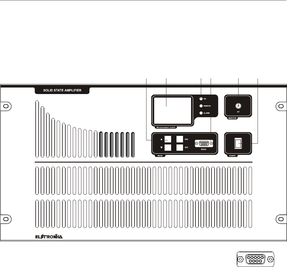
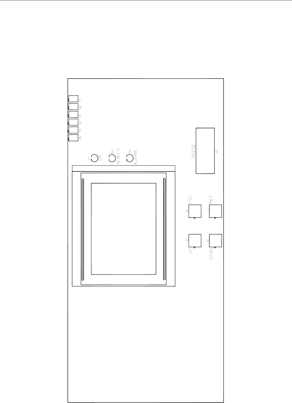
1.4 FRONT PANEL
2 3 51
1. Function keys
2. LCD Graphic Display
3. Status LEDs
4. RS232 Socket
5. RF Monitor Connector
6. Main Switch
64
RS232 for connection
to PC with ERCoS software
and for firmware upgrade
Pin 2: TX
Pin 3: RX
Pin 5: GND
98
FUSE
FUSE
FUSE
1
1.6 REAR PANEL
1. Breaker
2. AC 220V OUT Socket
3. AC 400V IN Socket
41. FAN 3.15A Fuse
42. CONTROL BOARD 1A Fuse
43. EXCITER 4/8A Fuse
5. RF IN Connector
6. RS485 Socket
7. EXCITER Socket
8. TELEMEASURES Socket
9. RF OUT Connector
62 35 97 8
Wired Telemeasures connector
Pin 1: FWD power (Analog out)
Pin 2: REF power (Analog out)
Pin 3: Temperature (Digital out)
Pin 4: Interlock (Digital in)
Pin 5: GND
Pin 6-7: Free contact (Digital out)
Closed when Alarm
Pin 8: 0V=ON / 5V=Normal (Digital in)
Pin 9: 0V=OFF / 5V=Normal (Digital in)
EXCITER for connection
to Driver Module
Pin 1: GND
Pin 2: 0V=Normal / 5V=AGC Alarm
(Digital out)
Pin 3: 0V=Normal / 5V=AGC Alarm
(Digital out)
Pin 8: FWD power (Analog out)
Pin 9: REF power (Analog out)
RS485 for connection
to RCU or Amplifier Control
Pin 2: RX- Pin 5: GND
Pin 3: RX+ Pin 7: TX-
Pin 4: +5V Pin 8: TX+
4243
41

99
Section 2 - Installation
Contents:
2.1 Operating environment
2.2 First installation
2.3 Connection with VEGA Transmitter
2.4 Stand-alone Amplifier configuration in Dual Drive version
2.5 Slave multi-Amplifier configuration with Amplifier Control
2.6 Stand-alone Amplifier configuration with Elettronika RCU
2.7 Stand-alone Amplifier configuration with direct PC connection
100
2.1 OPERATING ENVIRONMENT
You can install the equipment in a standard component rack or on a suitable surface such as a bench or desk.
In any case, the area should be as clean and well-ventilated as possible. Do not locate the equipment directly
above a hot piece of device. The upper lid can be dismounted to allow an easy internal access. The equipment
is designed with a modular design, that is each circuit is realized inside different modules or boards. All
interconnections between modules are made by means of connectable cables which allow an easy and quick
maintenance of demaged modules.
2.2 FIRST INSTALLATION
Correct installation of the equipment is important for maximum performance and reliability. Antenna and earth
connections must be installed with the greatest care. The equipment adjustment isn’t need, because the unit is
completely adjusted by our technical staff.
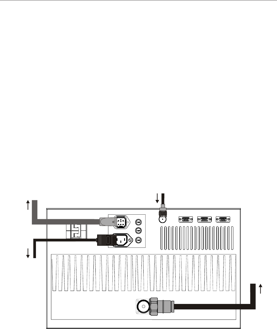
1. Connect Power Supply cable of the Exciter to the Auxiliary Socket on the rear panel of the Amplifier;
2. connect the Power Supply cable of the Amplifier to the electric network (230VAC Monophase or 400VAC
Threephase); if present the Isolator Transformer, the Amplifier is provided with cable and plug;
3. connect the RF OUT Exciter cable to the RF IN connector on the rear panel of the Amplifier;
4. connect the Antenna cable to the RF OUT connector on the rear panel of the Amplifier.
AGC
BREAKER
AC 200V OUT
RF IN RS485 TELEMEASURES
AC 400V IN
RF OUT
To ANTENNA
To ELECTRIC NETWORK
To EXCITER
RF INPUT
101
When the equipment is put within a combined system it is directly connected to the input splitting and output
combining systems.
Before fully powering the equipment, check that the output connections of the coaxial cable to the antenna
system are working.
In order to this it is possible to check the indication of the Reflected Power at low power levels. Only if the
SWR indication on the display is 0, the output power can be slowly increased. At maximum output power,
some watts might be shown as Reflected Power.
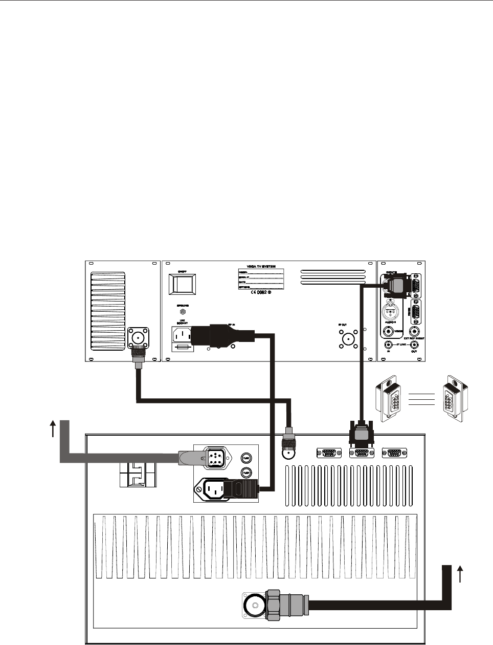
2.3 CONNECTION WITH VEGA TV TRANSMITTER
AGC
1
2
8
5
8
4
TV AMPLIFIER VEGA
BREAKER
AC 200V OUT
RS485 TELEMEASURES
AC 400V IN
RF OUT
RF IN
To ELECTRIC NETWORK
To ANTENNA
102
2.4 STAND-ALONE AMPLIFIER CONFIGURATION IN DUAL DRIVE VERSION
OUT
MAIN
VIDEO
OUT
AUX
AUXMAIN
GND
LEFT
OUT
AUX
LEFT
MAIN
LEFT
OUT
IN
RIGHT
OUT
AUX
RIGHT
MAIN
OUT
RIGHT
IN
IN
AUX
MAIN
IN
19kHz
OUT DIRECT
REMOTE
IN
RF AUX IN RF OUT RF MAIN IN
AUX CTRL
RS232/485
REMOTE
MAIN CTRL
BREAKER
AC 200V OUT
AC 400V IN
RF OUT
AGCRS485 TELEMEASURESRF IN
To ANTENNA
103
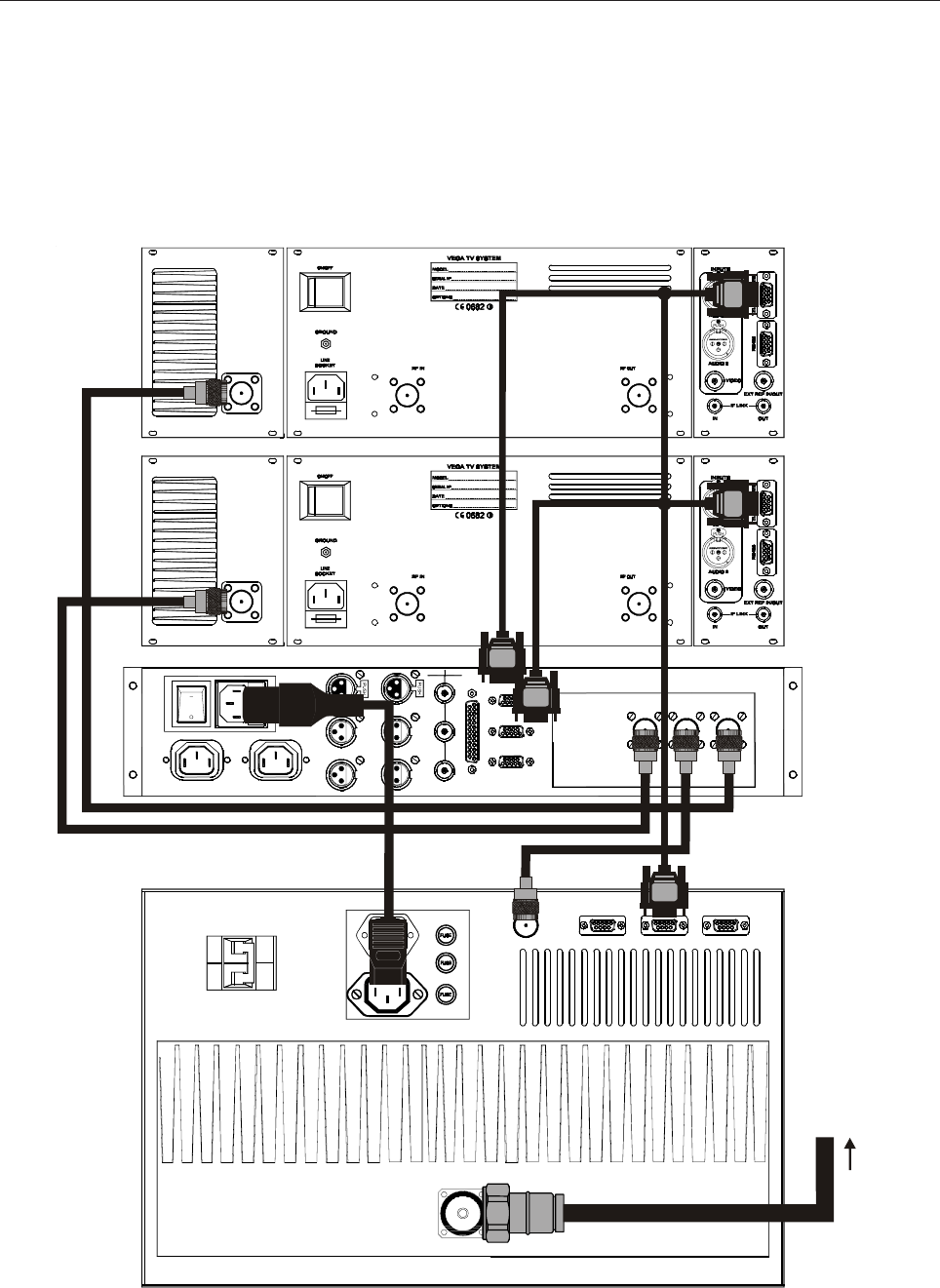
2.5 SLAVE MULTI-AMPLIFIER CONFIGURATION WITH AMPLIFIER CONTROL
BREAKER
AC 200V OUT
AC 400V IN
RF OUT
AGCRS485 TELEMEASURES
2
3
5
2
3
5
AMPLIFIER CONTROL AMPLIFIER
RF IN
To COMBINER
7
8
7
8
From SPLITTER
104
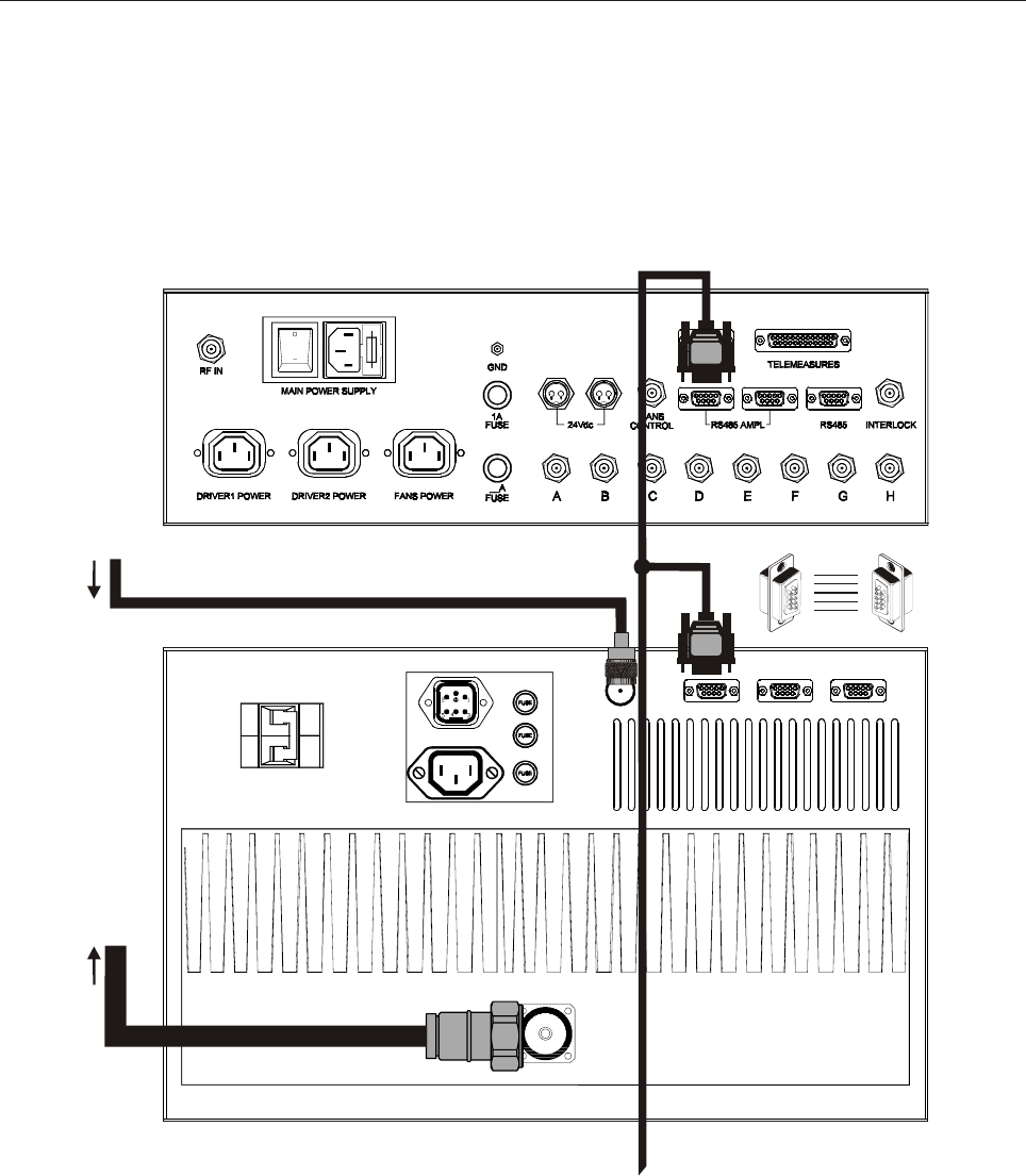
2.7 STAND-ALONE AMPLIFIER CONFIGURATION WITH DIRECT PC CONNECTION
2.6 STAND-ALONE AMPLIFIER CONFIGURATION WITH ELETTRONIKA RCU
SERIAL PORT
BREAKER
AC 200V OUT
AC 400V IN
RF OUT
AGCRS485 TELEMEASURESRF IN

105
Section 3 - Operation
Contents:
3.1 Operation
3.2 Display
3.3 Menus
3.4 Firmware upgrade
106
3.1 OPERATION
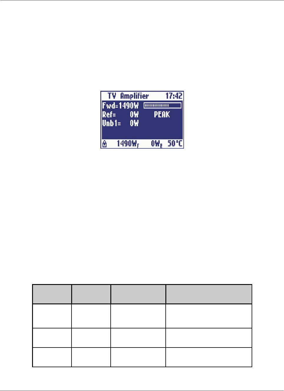
At startup, after initial image, the display shows the main screen with the RF powers as below:
The user may turn on and off the amplifier by means of the switch on the front panel. The control board turns
on all the power supplies, the exciter (if any), and internal cooling fans. While the amplifier is working, the
micro-controller monitors continuously the most important parameters: power supply voltages, absorbed
currents, high power zone temperature, forward and reflected powers, unbalances (if any). Each measure is
associated to a maximum threshold beyond which the amplifier is immediately put in protection status by
turning off one or more power supply, depending on the failed block. In order to prevent a temporary problem
to trigger a definitive protection status, the failed block is turned on again, after some seconds, for up to five
times. If it goes beyond the protection threshold for more than five times, it is declared as FAILED and it will
no longer be turned on. In this case, the amplifier will have to be turned off manually by means of the switch on
the front panel, then turned on again after performing the needed maintenance.
On the front panel there are also three LEDs labelled ON, REMOTE and ALARM. Their meanings are
explained in Table 1.
Table 1: Meanings of the three LEDs on the front panel
1 Screenshots in this manual are indicative, so they can be different from those on your equipment.
LED COLOUR MEANING MEANING WHEN BLINKING
ON Green The amplifier is on The amplifier has been turned on
locally but it has been turned off by
remote
REMOTE Yellow Remote control is
enabled It never blinks
ALARM Red An alarm is present It never blinks
107
3.2 DISPLAY
The Control Board is provided with a modern pixels graphic display with blue background. Normally it
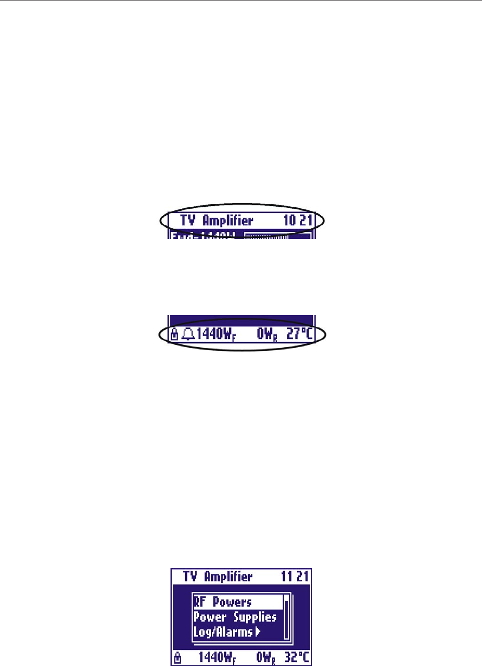
always shows a title bar (on the top line) and a status bar (on the bottom line). The ‘Title bar’, shows the name
of the amplifier (TV Amplifier) and the current time. If the amplifier is a single unit coupled externally with other
units in a high power transmitter, the title bar shows the amplifier number (slave address) too.
The ‘Status bar’ indicates the forward and reflected powers and the temperature. It also contains two symbols
for the interlock (lock) and the alarm (bell).
The bell symbol is continuously displayed in case of alarm. It blinks if there has been an alarm which has ended
but has not yet been seen by the user. It stops blinking once the Log has been checked. The interlock symbol
is displayed only when this function is enabled. It may be either a close lock, when there is no alarm (interlock
chain closed) or an open lock in case of alarm (interlock chain open).
Since the status bar is always showed on the display, regardless of the screen, the user may monitor at any
time the most important parameters and the presence of alarms while moving between different screens.
3.3 MENU
The user may see or modify locally some configuration parameters using the four buttons on the front panel.
All screens areorganized in a hierarchical menus and the user may move between them in a simple and intuitive
way. To see the menu it’s sufficient to press the ESC key.
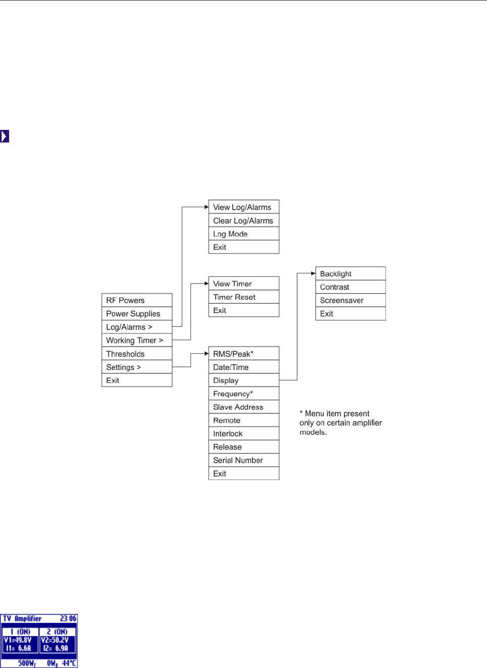
108
RF Powers
This is the main screen showing the RF powers of the amplifier: forward power, reflected
power, unbalances, if any. For forward power a level bar is displayed. See an example in
Figure 1.
Power Supply
This screen shows all the signals coming from two power supply. To check the next
(previous) power supply press the UP (DOWN) key. For each power supply, the voltage,
the absorbed current and the status (ON or OFF) are shown.
The display only shows three items at a time: all the items can be scrolled by the UP and DOWN arrow keys.
Any item can be chosen by selecting it and pressing the RET key. Menu entries with an arrow on the right
open sub-menus when chosen. Thus there is a hierarchical structure as below. To go back from a sub-menu
to the previous menu, press the ESC key. If the ESC key is pressed in the main menu, the RF powers screen
is accessed.
Hierarchical menu structure
109
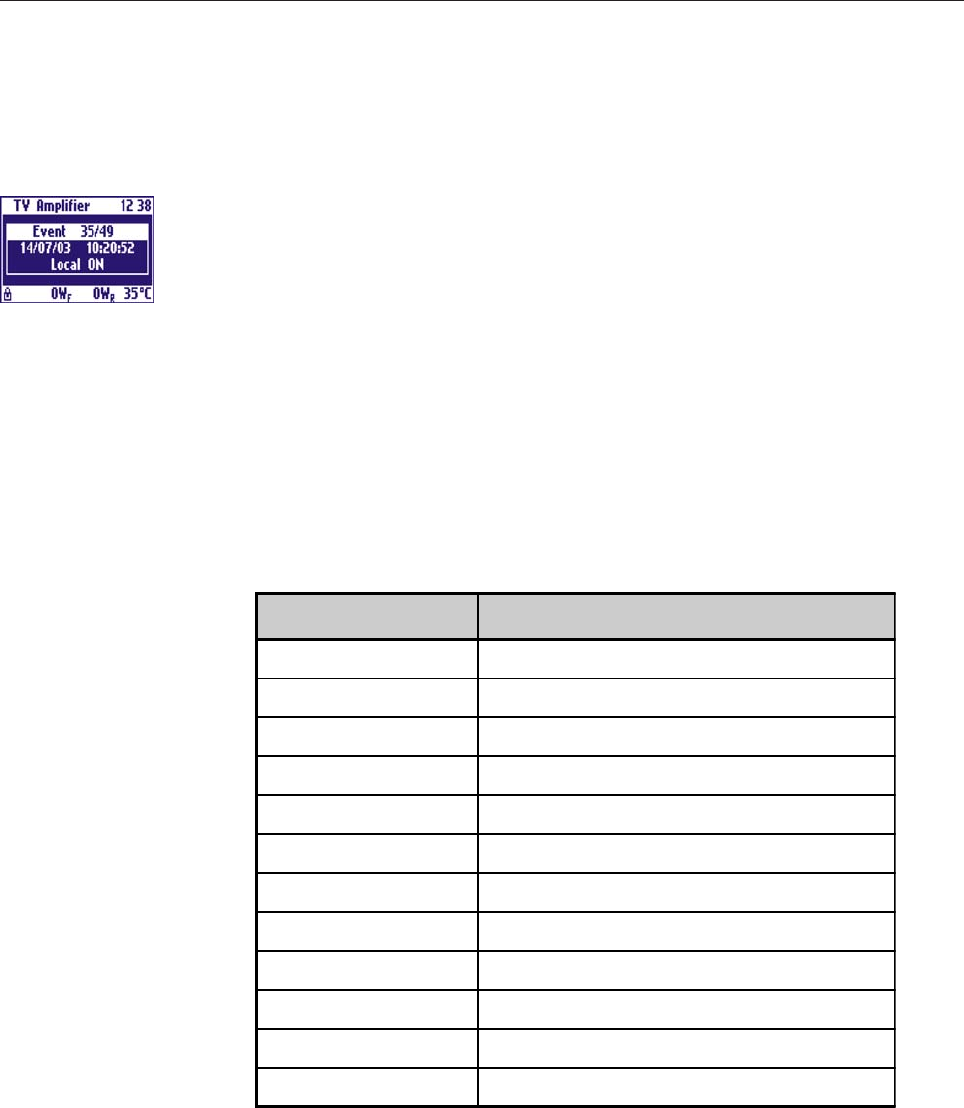
Log/Alarms
The control board is provided with an external EEPROM and a clock. Any alarm or
switching event with the time at which it occurred is saved in the EEPROM. The Log/
Alarms sub-menu allows to manage this log.
It is possible to see the events stored in the log by selecting Log/Alarms J View Log/
Alarms. All events can be scrolled by pressing the UP and DOWN keys. For example,
the event shown in Figure 7 is the turning on of the amplifier by means of the local switch.
For every event/alarm a short description and the date and time at which it occurred is
displayed.
In case of alarm, the value of the measure which caused the alarm is saved into the log. In
case of alarm still existing after five turning-on attempts, the parameter is marked as
FAILED. The table below is the list of all the events which can be logged.
EVENT DESCRIPTION
Local ON Amplifier turned on by means of the local switch
Local OFF Amplifier turned off by means of the local switch
Remote ON Amplifier turned on remotely
Remote OFF Amplifier turned off remotely
Interlock open Interlock chain open
Interlock closed Interlock chain closed
Power Supply ON Power supply on
Fwd Pwr xxxxW Alarm for forward power
Ref Pwr xxxxW Alarm for reflected power
UnbY xxxxW Unbalancing alarm
V1 xx.xV Power supply voltage alarm
I1 xx.xA Power supply current alarm
The log may be completely deleted by selecting Log/Alarms J Clear Log/Alarms.
Amplifier can store in the log details about alarms and generic events. You can change this
behaviour selecting Log/Alarms J Log/Mode menu item.
Working Timer
The control board has a working timer which is always enabled while the amplifier is
110
working (i. e. there is at least one power supply working). The menu entry Working
Timer J View Timer allows to check the hours for which the timer has been enabled.
Working Timer J Timer Reset resets the timer.
Thresholds
This is a screen showing the alarm threshold of each signals monitored by the control
board. The list can be scrolled by means of the UP and DOWN keys.
RMS/Peak
The control board can monitor both the RMS and peak powers, the first used in digital
systems. The menu entry Settings J RMS/Peak allows to choose the power to be displayed
and monitored. This menu is present only in certain amplifiers.
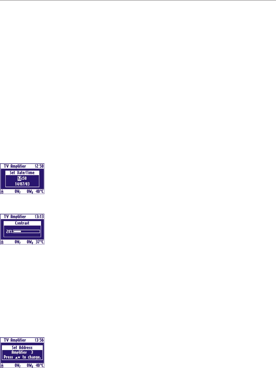
Date/Time
This screen allows to set the current date and time. The setting is changed by pressing the
arrow keys, then pressing the RET key to move to the following value and eventually
save the changes. To go back to the previous menu and discard any change made, press
the ESC key.
Display
The menu entry Settings J Display allows to change some settings of the display, such
has back light, contrast and screensaver. The back light and the contrast are set by means
of the UP and DOWN arrow keys. The changes made are saved by pressing the RET
key or discarded pressing the ESC key.
With Settings J Display J Screensaver you can set an interval time after which display
backlight is turned off. When display backlight is off, press any key to switch it on.
Frequency (only for some Amplifiers)
The forward and reflected RF powers is measured by means of a directional coupler. In
order to compensate for the effect due to the sampling made by the coupler, it is possible
to set the frequency by menu entry Settings J Frequency. The setting can be changed by
pressing the arrow keys. The changes made are saved by pressing the RET key or
discarded pressing the ESC key. Set the video carrier frequency.
Slave Address
The amplifier may be used either in stand-alone mode or as a slave of a master in a high
power multiple units transmitter. In the latter case an unique address for each amplifier
has to be specified, in order for all of them to communicate with the master on the same
RS485 bus. The menu entry Settings J Slave Address allows to choose the stand-

111
alone mode or set a slave address by means of the UP and DOWN arrow keys. The
changes made are saved by pressing the RET key or discarded pressing the ESC key.
Remote
The amplifier may be controlled either locally, by means of the keys and display, or
remotely. There are three possibilities for remote control:
- using a direct serial connection between amplifier RS232 connector and a PC RS232;
- using the remote control device manufactured by Elettronika S.r.l. (RCU), on the RS485;
- using a general-purpose control system connected to telemeasures.
You can enable / disable remote control choosing menu item Settings J Remote. When
remote control is enabled, the yellow REMOTE LED on the front panel is lit.
Interlock
One of the pins of the telemeasure connector, located on the rear panel, is used for the
interlock alarm. It is an input line which turns off the amplifier in case of alarm. The
interlock check can be enabled or disabled using menu item Settings J Interlock. When
it is enabled, the status bar shows the lock symbol, which is close if the interlock chain is
closed (no alarm) or open if it is open (alarm).
Firmware Release
The menu entry Settings J Firmware Release allows to display the firmware version
number and the hardware release of the amplifier.
Serial Number
The menu entry Settings J Serial Number allows to display the serial number of the
apparatus.
112
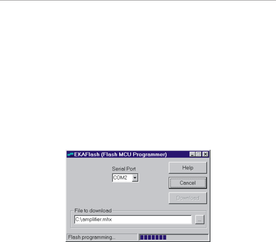
3.4 FIRMWARE UPGRADE
The microcontroller is provided with a built-in Flash memory containing the firmware. The firmware can be
updated with a later version without removing the apparatus from the rack and/or replacing the chip.
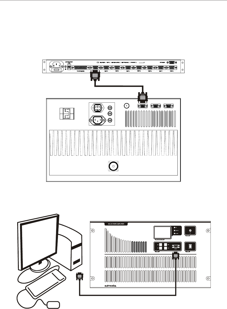
To upgrade it, connect a PC to the RS232 socket on the front panel of the apparatus by means of a cable
DB9 male - DB9 female (pin-to-pin).
Launch on the PC the EKAFlash application, select the serial port in use on the PC, choose the update file by
pressing the “...” key and click on Download button.
Eventually, turn off the amplifier from the main switch and then turn it on again. The upgrade of the firmware
begins on the EKAFlash window. The figure below shows this window while a firmware is being updated.
The EKAFlash window while updating a firmware

113
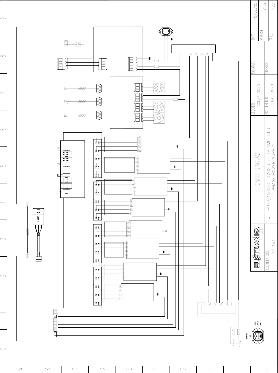
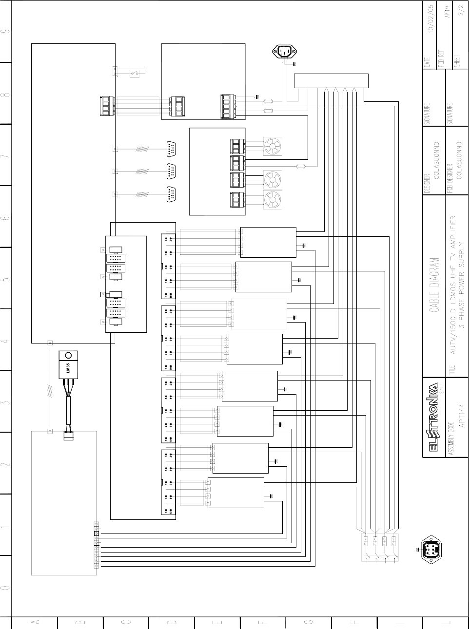
Section 4 - Diagram
Contents:
- APT144 AUTV/1500LD Cable diagrams
- APT144C_APT144CM AUTV/1500LD Component list
- APT144DM_APT144DM/DIG AUTV/1500LD Component list
- Modules description
114
FAN
3.15A
FAN
TP1
TP2
TP5
TP3
TP4
TP6
TP7
TP10
TP8
TP9
J3J7 J6
J19
TEMP+5V
TEMP+5V
J21
J2
AUXILIARY SOCKET
1A
5A
+24VGND
1
J14
234 J15
U21
U19 U19
U21
U8
U7
U5
U6
U3
U4
U1
U2
U14U14
1
2
4
3
8
7
6
5
8
7
6
3
4
5
1
2
T1
T2
T3
S1
S2
R1
R2
S3
R3
N
N
N7
N6
N8
N3
N2
N4
N5
N1
N10
N9
N 0
N (EQUIPOTENTIAL)
1
2
4
3
5
6
8
7
T1
N8
N7
T2
N6
T3
S1
N5
N4
S2
S3
N3
R1
N2
R2
N1
R3
R31
R32
R31
R33
R33
N 0
N10 N11
N9 N91 N91
FAN
L (EQUIPOTENTIAL)
HANDLE ACTUATOR SW.
SCH0221A
AMPLIFIER INTRFACE BOARD
SCH0223A
CONTROL BOARD AND DISPLAY
EXCITERRS485 TELEMEASURES
J9J10J11
U9
U10
U11U11
U10
U9
J4
J2
9
J1
1
J3
910
21
10
2
J7
J5
J6
9
1
10 9
2 1
J8
10
2
MAIN SWITCH
SCH0288A
INTERFACE BOARD
J3
J6J1 J8 J12
POWER SUPPLY #1
POWER SUPPLY #2 POWER SUPPLY #4
POWER SUPPLY #3
RF MONITOR
4
V- L NV+ 5
V-V+ LN
V+ V- L N
V+ NLV-
SWITCHING
SP500-27/48
POWER SUPPLY
6
Im
COM
R.C.
SP500-27/48
8
V+ V- L N
POWER SUPPLY
SWITCHING
Vm
Im
POWER SUPPLY
SP500-27/48
7
R.C.
Vm
Im
COM
SWITCHING
Vm
SWITCHING
POWER SUPPLY
SP500-27/48
COM
R.C.
Vm
Im
COM
SP500-27/48
SWITCHING
POWER SUPPLY
R.C.
Vm
Im
COM
R.C.
SP500-27/48
POWER SUPPLY
SP500-27/48
V+
L
3
V-V+ N
V+ V-
2
V- N
L1
LN
SWITCHING
COM
POWER SUPPLY
R.C.
Vm
Im
COM
POWER SUPPLY
SWITCHING
SP500-27/48
Vm
SWITCHING
Im
R.C.
COM
Vm
Im
R.C.
ZNLNZL
NZLLN
J3 J2 J1 J8
PN1114A
FANS CABLE BOARD
J1
GDLNF
J2
SCH0265A
MAINS DISTRIBUTION BOARD
115
ZNLNZL
NZLLN
J3
EXCITERRS485 TELEMEASURES
HANDLE ACTUATOR SW.
4
V- LNV+ 5
V-V+ L N
V+ V- L N
V+ NLV-
SWITCHING
SP500-27/48
POWER SUPPLY
6
Im
COM
R.C.
SP500-27/48
8
V+ V- L N
POWER SUPPLY
SWITCHING
Vm
Im
POWER SUPPLY
SP500-27/48
7
R.C.
Vm
Im
COM
SWITCHING
Vm
SWITCHING
POWER SUPPLY
SP500-27/48
COM
R.C.
Vm
Im
COM
SP500-27/48
SWITCHING
POWER SUPPLY
R.C.
Vm
Im
COM
R.C.
SP500-27/48
POWER SUPPLY
SP500-27/48
V+
L
3
V-V+ N
V+ V-
2
V- N
L1
LN
FAN
3.15A
FAN
SWITCHING
COM
POWER SUPPLY
R.C.
Vm
Im
COM
POWER SUPPLY
SWITCHING
SP500-27/48
Vm
SWITCHING
Im
R.C.
COM
Vm
Im
R.C.
TP1
TP2
TP5
TP3
TP4
TP6
TP7
TP10
TP8
TP9
J3J7 J6
J19
TEMP+5V
TEMP+5V
J21 J3
J2
J9J10J11
AUXILIARY SOCKET
1A
5A
J1
GDL NF
J2
+24VGND
MAIN SWITCH
1
J14
234 J15
J6
J4
J2
9
J1
1
J3
910
21
10
2
J1
J7
J5
SCH0288A
J6
9
1
10 9
2 1
J8
10
2
J8 J12
1 = NC
400VAC
3 = R
4 = S
5 = T
2 = N
NRST
U21
U19 U19
U21
U9
U10
U11
U8
U7
U5
U6
U3
U4
U1
U2
U14U14
1
2
4
3
8
7
6
5
8
7
6
3
4
5
1
2
U11
U10
U9
T1
T2
T3
S1
S2
R1
R2
S3
R3
N
N
N7
N6
N8
N3
N2
N4
N5
N1
N10
N9
N 0
N (EQUIPOTENTIAL)
1
2
4
3
5
6
8
7
T1
N8
N7
T2
N6
T3
S1
N5
N4
S2
S3
N3
R1
N2
R2
N1
R3
R31
R32
R31
R33
R33
N 0
N10 N11
N9 N91 N91
FAN
INTERFACE BOARD
J2 J1 J8
PN1114A
FANS CABLE BOARD SCH0265A
MAINS DISTRIBUTION BOARD
SCH0221A
AMPLIFIER INTRFACE BOARD
SCH0223A
CONTROL BOARD AND DISPLAY
POWER SUPPLY #1
POWER SUPPLY #2 POWER SUPPLY #4
POWER SUPPLY #3
RF MONITOR

116
Elettronika Code Description Qty Page 1/2
00664 LM35DT THERMAL SENSOR 1
01041 1nF 50V CERAMIC CAPACITOR 2
02228 N FEMALE CONNECTOR 1 (APT144CM)
02502 SMA SOCKET FOR RG58 1
02695 DB9 CONNECTOR FOR IU008059 CABLE 3
02699 FEMALE 10WIRE CONNECTOR 9
02700 FEMALE 16WIRE CONNECTOR 1
02830 10A GREEN PLUG 1
02876 5 POLES 16A ILME AC SOCKET 1 (APT144CM)
02877 5 POLES 16A ILME SOCKET PANEL MOUNTING 1 (APT144CM)
02893 3 WAY MALE EXTRACTABLE TERMINAL BLOCK 4 (APT144CM)
02894 3 WAY FEMALE EXTRACTABLE TERMINAL BLOCK 4 (APT144CM)
05064 FERRITE 8 (APT144CM)
05553B 5-6U HANDLE KIT 2
07515C 4x16A AUTOMATIC SWITCH 1 (APT144C)
07524A SWITCH 1
07541 10A FUSE-HOLDER PANEL MOUNTING 3
07605C FAN 3
07605D 1.5uF 400V CAPACITOR 3
07605F GRID FAN 6
07925 PVC PROTECTION 1
08503 RG 303 50W TEFLON CABLE 1.20
09419 PN419/A PRINTED CIRCUIT BOARD 1
CON0245 CON0245R1 MECHANICAL DETAIL 1
CON0249 CON0249R0 MECHANICAL DETAIL 1
CON0276 CON0276R3 MECHANICAL DETAIL 1
CON0277 CON0277R3 MECHANICAL DETAIL 1
CON0280 CON0280R2 MECHANICAL DETAIL 1
C0205 MULTIPOLES WIRE 3.00
DET0516 DET0516R0 MECHANICAL DETAIL 1
DET0575 DET0575R1 MECHANICAL DETAIL 8
DET0772 DET0772R0 MECHANICAL DETAIL 2
DET0798 DET0798R0 MECHANICAL DETAIL 6
DET0996 DET0996R0 MECHANICAL DETAIL 1
DET1022 DET1022R0 MECHANICAL DETAIL 1
DET1054I DET1054R1 MECHANICAL DETAIL 2
DET1185 DET1185R1 MECHANICAL DETAIL 2
E0012 SP-500-27 DE2 SWITCHING POWER SUPPLY 8
FUS1A 1A FUSE 1
FUS3A 3.15A FUSE 1
FUS5A 5A FUSE 1
MTF0070CR0 LDMOS UHF AMPLIFIER MODULE 1
PAN0074 PAN0074AR2 FRONT PANEL 1
PN1114A PN1114AR1 PRINTED CIRCUIT BOARD 1
R0012 18mm DIAMETER WHEEL 8
Component list APT144C_APT144CM

117
Elettronika Code Description Qty Page 2/2
SCH0223AR1 CONTROL BOARD AND DISPLAY 1
SCH0265AR0 MAINS DISTRIBUTION BOARD 1
SCH0288AR1 POWER SUPPLY INTERFACE BOARD 1
V0760 BLACK PLASTIC TAP 1 (APT144CM)
V0962 TERMINAL BLOCK 3 (APT144CM)
Z0021 MECHANICAL DETAIL 2
Z0081 MECHANICAL DETAIL 1
Z0673 COVER 1

118
Elettronika Code Description Qty
02029 UG909 CONNECTOR FOR RG 58 CABLE 1
02410 7/16” CONNECTOR FOR 1/2” CABLE 1
02450 EIA 7/8” CONNECTOR FOR 1/2” CABLE 1
02458 EIA 7/8” INNER 1
02502 SMA SOCKET FOR RG58 CABLE 1
02791 DB9 MALE SOCKET PANEL MOUNTING 5 (APT144DM) 2 (APT144DM/DIG)
02871 DB9 SHELL 5 (APT144DM) 2 (APT144DM/DIG)
06674 UHF ATV BANDPASS FILTER 1 (APT144DM)
06676A UHF DTV BANDPASS FILTER 1 (APT144DM/DIG)
07595 FAN 1
07595A 6uF CAPACITOR 1
07595B GRID 1
07596 GRID 1
08504 RG 58 50Ω CABLE 1.00
08515C 1/2” CABLE 1.00
APT144CM AUTV/1500LD LDMOS UHF TV AMPLIFIER 1
CMS6006 1m 1/2” CABLE FOR 7/16” MALE CONNECTOR 1
CSS5011 1.5m RG 58 CABLE FOR N - N MALE CONNECTOR 1
DET0434 DET0434R2 MECHANICAL DETAIL 1
DET0536 DET0536R3 MECHANICAL DETAIL 2 (APT144DM)
DET0564 DET0564R0 MECHANICAL DETAIL 1
DET0565 DET0565R0 MECHANICAL DETAIL 1
DET1028 DET1028R0 MECHANICAL DETAIL 2 (APT144DM/DIG)
DET1051 DET1051R0 MECHANICAL DETAIL 2 (APT144DM)
DET1069 DET1069R0 MECHANICAL DETAIL 2 (APT144DM)
PAN0080 PAN0080R0 1U FRONT PANEL 1 (APT144DM)
PAN0081 PAN0081R0 2U FRONT PANEL 1 (APT144DM) 2 (APT144DM/DIG)
PAN0082 PAN0082R0 3U FRONT PANEL 3 (APT144DM) 2 (APT144DM/DIG)
R0159 20U RACK 1
Z0114 MECHANICAL DETAIL 1
Z0500 MECHANICAL DETAIL 8
Component list APT144DM_APT144DM/DIG
119
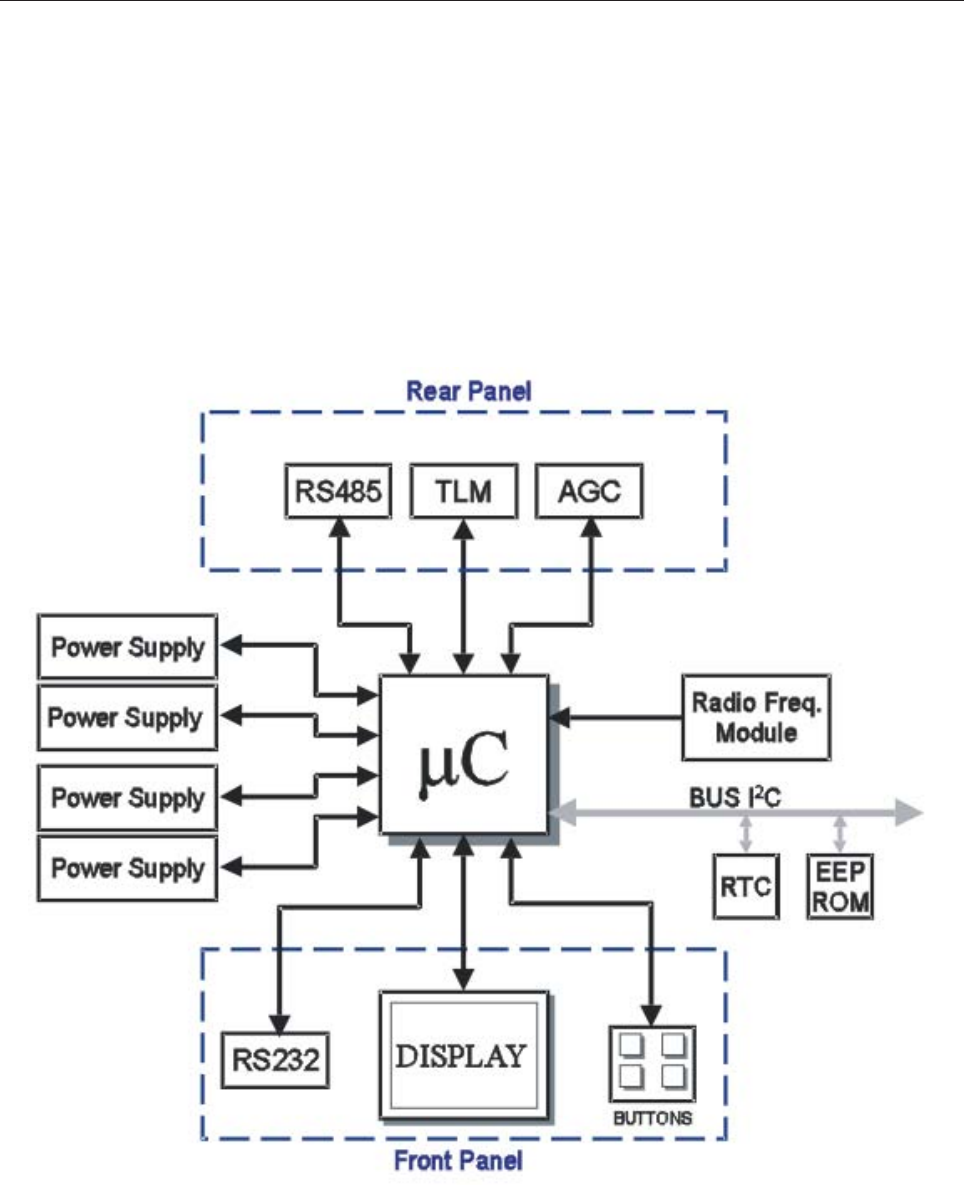
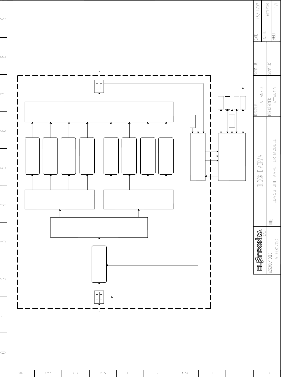
Figure 1: Simplified block diagram of the control and display board
CONTROL BOARD SCH0223AR1
DESCRIPTION
The Control Board SCH0223A manages the operational logic of the amplifier: switching on and off, power
supply and fans, alarms and protections, remote control, human-machine interface. All of that is performed by
a modern and powerful 16 bit micro-controller, which is the main part of the board.
120
It can be seen that the micro-controller is the heart of the control system, to which the various peripherals
(power supply, serial ports, telemeasure socket, AGC port, RF amplifier module, ROM, clock, display and
keys) are interfaced.
- Power Supply
The board is powered with a continuous +24V voltage applied on the J14 connector. From that the +5V
voltage, powering the most of the chips (micro-controller, operational amplifiers, display, etc.) is derived by
means of a switching converter (see IC19). A +12Vdc voltage is obtained from it as well, by means of a linear
conversion provided by the integrated circuit IC8. From this, a -12Vdc voltage is obtained by means of the
integrated circuit IC5. The -12V voltage is used to adjust the contrast of the display.
- Connectors
On the board SCH0223A there are several connectors used as interfaces for the peripherals of the apparatus
and the ports for external communication.
POWER SUPPLY
The connectors J1, J6, J8 e J12 are used to connect the power supply powering the RF modules. The number
of power supply used changes depending on the amplifier, up to eight power supply. They are connected in
the order shown in Table 1 below. Remaining connectors, if any, are left unconnected.
Table 1: Interface connectors for the power supply
Through this connection, each power supply provides the level of voltage and current acquired by the micro-
controller by means of an internal ADC. Besides the connectors allow the control board to turn on or off the
individual power supply (for instance when an alarm occurs).
RF AMPLIFICATION
The J3 connector interfaces the control board with the RF amplification section. Through this connector the
CONNECTOR POWER SUPPLY N°
J1 1 - 2
J6 3 - 4
J8 5 - 6
J12 7 - 8
121
micro-controller acquires the forward and reflected powers, unbalancing (if any), and temperature of the
critic amplification area. It also allows to inhibit the transistors in case of reflected power alarm, by means of
a totally hardware, thus extremely fast protection.
Depending on the apparatus, this connector may also allow to enable or disable the cooling fans of the critic
area.
RS485
The J11 connector (10 pin socket) is directly wired to a DB9 female connector placed on the rear panel of the
apparatus. This communication bus allows to connect the amplifier to the control (Amplifier Control) module
of a high-power transmitter composed by several individual amplifiers. In this case, each amplifier and the
Amplifier Control are connected to the same 4-wires RS485 bus and each of them has a unique address
(which can be set by means of the keys and the display) for correct communication.
In case of single (stand-alone) amplifier, the RS485 connector can be used to interface to the Remote Control
Unit (RCU) made by Elettronika S.r.l. This unit allows to monitor and control the remote transmitter from any
site provided with PSTN or GSM1 phone connection.
Table 2 shows the wiring between the J11 connector on the board and the DB9 female connector on the rear
panel, along with the description of the lines.
1 For more details about the control system contact the distributor or the manufacturer.
PIN N°
ON DB9 PIN N°
ON J11 DESCRIPTION
11 Not used
23 Rx-
35 Rx+
47 +5V
59 GND
62 Not used
74 Tx-
86 Tx+
98 Not used
Table 2: Description of the RS485 connector
122
TELEMEASURES
The J9 telemeasure connector (10 pins socket) is directly wired on a DB9 female connector placed on the
rear panel. There are input and output digital lines (TTL level) and analog output lines on this connector, which
are used to monitor and control the amplifier by means of a general-purpose remote control system.
The correspondence between the pins of the J9 connector on the board and the DB9 female connector on the
rear panel, as well as the meaning of the various lines, is shown in table 3 below (the directions are in respect
to the micro-controller on the board).
Table 3: Description of the telemeasures connector
The input stage of the digital pins has an internal pull-up towards the 5V power supply voltage. To use these
lines it only takes setting a switch to close to earth. When closed, the relevant control (turning on or off) is
enabled and the switch may be open again (impulse controls).
The interlock pin may be used as protection so that the amplifier is switched off when the digital input level is
low. It is possible to use several serially connected switches to make an interlock chain. Usually all switches
are closed and the interlock level is low, thus the amplifier is on. If even only one of the switches is open, the
(*)
(*)
(*) You can select by means of two jumpers on the board (JP1 and JP2) RMS or peak power. If there are two jumpers on pins 1 and 2 of
JP1 and JP2 connectors, RMS power is selected. Otherwise, if there are two jumpers on pins 2 and 3 of the same connectors, peak power
is selected.
PIN N°
ON DB9 PIN N°
ON J9 TYPE DIRECTION DESCRIPTION
1 1 Analog Output Forward power
2 3 Analog Output Reflected power
3 5 Analog Output Temperature
4 7 Digital Input Interlock:
0V = Interlock Alarm
5V = Normal
59- -Ground
6-7 2-4 Digital Output Free Contact
(closed when amplifier is in alarm)
8 6 Digital Input Turning-on control
(normally high, active when low)
9 8 Digital Input Turning-off control
(normally high, active when low)
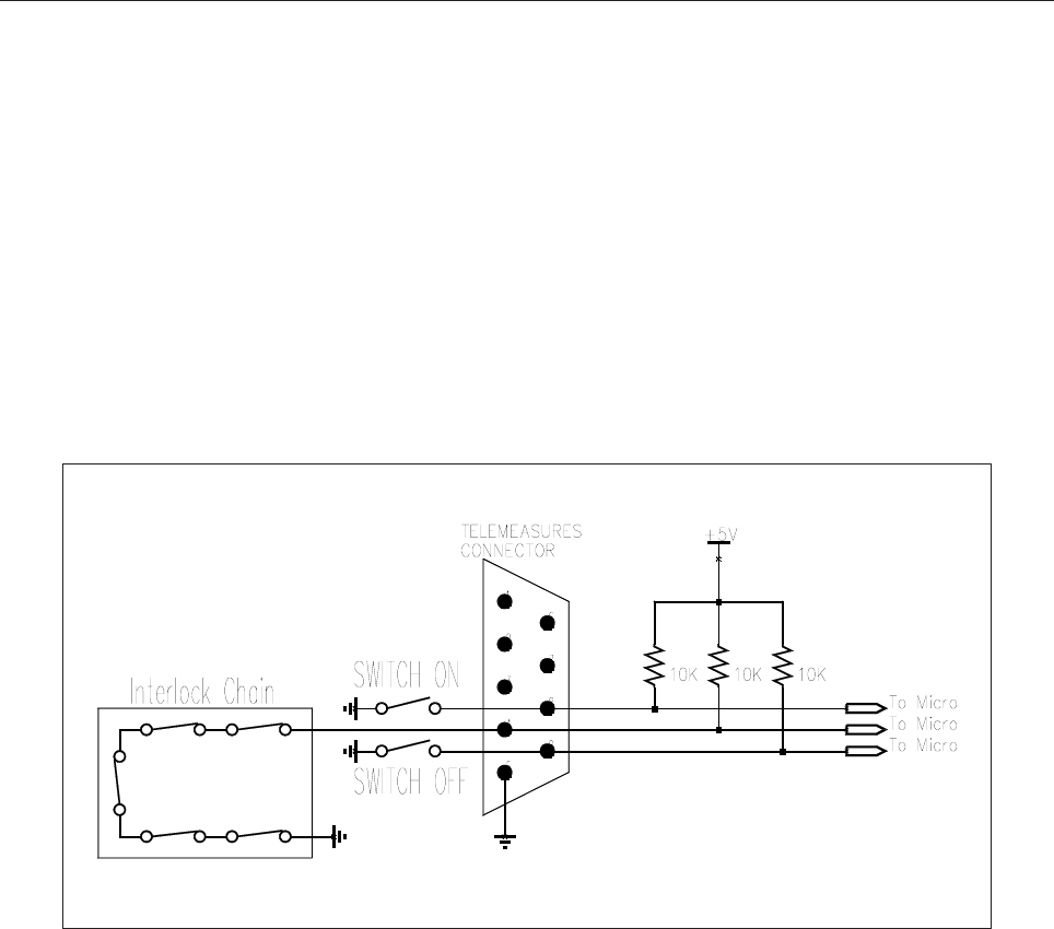
123
Figure 2: Usage of the digital input signals of the telemeasures connector
AGC / EXCITER
The connector called J10, as the telemeasures connector and the RS485 bus, is wired to a DB9 female
connector placed on the rear panel of the amplifier. This connector allow the implementation of an automatic
gain control between an exciter and the amplifier. A voltage signal related to the forward output power
supplied by the amplifier is provided through two pins of the AGC connector. Connecting one of these to the
relevant input pin of the exciter, this can pursuit a given voltage level, so that the output power is always
constant. In order to avoid that, in case of an alarm decreasing the forward power, the exciter increases its
output level due to the AGC, thus damaging the amplification stages, the connector is provided with two
digital output lines called AGC Alarm. Under alarm conditions, this lines are brought by the micro-controller
at a low level, so that the exciter can stop the AGC.
Table 4 shows the connection between the J10 connector on the board and the DB9 connector on the rear
panel, along with the description of each pin (the direction of the pin is referred to the position of the micro-
controller on the board).
level of the interlock signal becomes high (this line has a pull-up towards the +5V power supply voltage as
well) and the interlock protection activates switching off the amplifier. Note that in case the interlock protection
is not used, the pin 4 of the DB9 telemeasure connector and the earth pin (pin 5) must be short circuited.
Otherwise it is possible to disable the monitoring of the interlock chain from menu (see user manual).
Figure 2 shows a typical usage for the digital input signals to turn on and off the amplifier and for the interlock
alarm.
124
Table 4: Description of the AGC connector
RS232
The DB9 female connector on the front panel is an external communication RS232 serial port, through which
a PC can be connected directly to the amplifier in order to perform operations such as the remote control (by
means of an adequate software2) and the update of the microcontroller firmware.
The used communication protocol is asynchronous, at a 19200bps speed, 1 start bit, 8 data bits, 1 stop bit,
no parity. No hardware flow control is used. The connector is DCE type and the pin used are shown in Table 5.
PIN N° ON DB9 123456789
DESCRIPTION -TxDRxD-GND- - - -
MISCELLANEOUS
The J2 (called AUX), J4, J5 and J17 connectors are not used and are there only for future updates. The SW1
dip-switches are partially used for the configuration of the correct mode for the micro-controller. The other
switches are not used. It is important that the position of the dip-switches is left unchanged, because changing
it may set a wrong mode for the micro-controller, affecting the work of the whole amplifier.
2 For more information about this application contact the distributor of the manufacturer.
PIN N°
ON DB9 PIN N°
ON J10 TYPE DIRECTION DESCRIPTION
1 1 - - Ground
23DigitalOutput
AGC Alarm
0V = Alarm
5V = Normal
35DigitalOutput
AGC Alarm
0V = Alarm
5V = Normal
47- -Not used
59- -Not used
62- -Not used
7 4 - - Nout used
8 6 Analog Output Forward power
9 8 Analog Output Forward power
Table 5: Description of the RS232 connector
125
SCH0223AR1 Top layer Component layout
126
SCH0223AR1 Bottom layer Component layout

127
SCH0223AR1 COMPONENT LIST
Part Name/Number Description Qty. Comps. Page 1/2
BATT BH001RB 3093_90 03093 03090 BATTERY HOLDER 1 BATT1
CC 100nF-S 01065C 01065C Y5V 1206 CAPACITOR 46 C2, C7-10, C12, C16, C19, C21-27, C29, C31,
C33, C37-40, C44-46, C49, C58-61, C63, C65,
C66-69, C74, C76, C78-81, C83-84, C87, C90
CC 15pF-S 01088 01088 SMD 1206 CAPACITOR 4 C13-15, C17
CC 1nF-S 01096 01096 SMD 1206 CAPACITOR 7 C3-6, C50-51, C53
CC 1uF100V-S 01760A 01760A 1206 50V CAPACITOR 11 C1, C18, C28, C36, C43, C54, C62, C73, C77,
C88-89
CC 47pF-S 01100 01100 SMD 1206 CAPACITOR 2 C42, C52
CE 100uF25V-S 01793B 01793B ELET. SMD CAPACITOR 2 C11, C47
CE 10uF16V-S 01626B TANT. ELET. SMD CAP. 2 C56-57
CE 10uF35V-S 01778A 01778A ELET. SMD CAPACITOR 2 C20, C32
CE 1uF35V-S 01613A 01613A TANT. ELET. SMD CAP. 5 C70-72, C75, C82
CE 220uF50V LOW ESR 01799A ELET. SMD CAPACITOR 4 C55, C64, C85-86
CE 22uF16V-S 01780A ELET. SMD CAPACITOR 4 C34-35, C41, C48
CE 47uF35V-S 01790A 01790A ELET. SMD CAPACITOR 1 C30
D 1N4148-S 03002 03002 SMD DIODE 7 D1-2, D5-9
D 50WQ06FN 03019A SMD DIODE SCHOT. 5.5A 1 D23
D BAS85-S 03024 SMD DIODE SCHOTTKY 2 D14-15
D BAT54S 03199 SMD SCHOTTKY DIODE 19 D3-4, D10-13, D16-22, D24-29
DIS MGLS12864T 03083A 128x64 DOT 1 DIS1
DL KA-3528SGC 03057 03057 GREEN SMD LED DIODE 7 DL2, DL5-10
DL LEDG5 03060 03060 GREEN LED DIODE 5mm 1 DL1
DL LEDR5 03061 03061 RED LED DIODE 5mm 1 DL4
DL LEDY5 03054B 03054B YELLOW LED DIODE 5mm 1 DL3
IC 24LC64 04815 04815 SMD INTEG CIRCUIT 1 IC17
IC 78M12 4307B 04307B SMD VOLTAGE REGUL. 1 IC8
IC CD4051BM-S 04615 SMD INTEG CIRCUIT 3 IC7, IC14, IC23
IC LM2596S-5.0 04580 SMD INTEG CIRCUIT 1 IC19
IC LM358M-S 04660 04660 SMD INTEG CIRCUIT 1 IC3
IC LM393-S 04639 04639 SMD INTEG CIRCUIT 1 IC2
IC LMC6482-S 04632 SMD INTEG CIRCUIT 1 IC24
IC LMC6484-S 04634 SMD INTEG CIRCUIT 7 IC1, IC4, IC6, IC9, IC13, IC18, IC25
IC M41T56 04611 04611 SMD INTEG CIRCUIT 1 IC20
IC MAX232-S 04804B 04804B SMD INTEG CIRCUIT 1 IC21
IC MAX3080-S 04770 04770 SMD INTEG CIRCUIT 1 IC22
IC MAX942CSA-S 04572 SMD INTEG CIRCUIT 1 IC10
IC MB90F543PF 04596 SMD INTEG CIRCUIT 1 IC11
IC MPC100-450DI-TO 04608 INTEG CIRCUIT 1 IC16
IC TC7662BCOA 04758A 04758A SMD INTEG CIRCUIT 1 IC5
IC ULN2003A 4870 04870 SMD INTEG CIRCUIT 2 IC12, IC15
IND 2u2H-S 05020A 05020A INDUCTOR 1 L1
IND MS85 10uH-S 04948 2.7A INDUCTOR 1 L2

128
Part Name/Number Description Qty. Comps. Page 2/2
IND T100uH-1.8A 4958 04958 TOROIDAL-STORAGE 1 L3
J CON HD515V/05-4PVE 02881+02882 PANDUIT PCB CON. 1 J14
J DB9_F-0° LT 02794 PCB CONNECTOR DB9 1 J13
J FC-10P 02697-02699 02697+02699 PCB CONNECTOR 8 J1-2, J6, J8-12
J FC-16P 02701-02700 02701+02700 PCB CONNECTOR 1 J3
J PAN2 02739 02739 PCB CONNECTOR 2 J5, J7
J PAN2 02739-40-41 02739+02740+02741 PCB CONNEC. 1 J15
J PAN8 02716 02716 PCB CONNECTOR 1 J4
JU JUMP2 02739-02742 02739+02742 PAN2 MALE 1 JP3
JU JUMP3 02707-02742 02707+02742 PAN3 MALE 2 JP1-2
R 100K-1%-S 00065B 00065B RES 1/4W 1% SMD 1206 16 R33-34, R62-63, R78-79, R94-101, R106-107
R 100R-1%-S 00029D 00029D RES 1/4W 1% SMD 1206 12 R24, R47, R58, R71, R75, R81, R83, R89,
R103-105, R113
R 10K-1%-S 00053B 00053B RES 1/4W 1% SMD 1206 24 R7, R10, R12, R14-16, R22, R25, R27, R30,
R36, R38, R51, R64, R84-85, R87-88, R92,
R93, R108-111
R 10R-S 00017A 00017A RES 1/4W 5% SMD 1206 1 R68
R 1206 N. M. N. M. RES 1/4W 5% SMD 1206 1 R91
R 1K0-1%-S 00041B 00041B RES 1/4W 1% SMD 1206 8 R17, R54, R59-60, R76-77, R86, R90
R 22K-1%-S 00057B 00057B RES 1/4W 1% SMD 1206 11 R9, R21, R26, R28-29, R37, R45, R48-50, R69
R 2K2-1%-S 00045B 00045B RES 1/4W 1% SMD 1206 3 R52, R55, R61
R 330K-1%-S 00071D 00071D RES 1/4W 1% SMD 1206 1 R66
R 330K-S 00071A 00071A RES 1/4W 5% SMD 1206 1 R65
R 470K-S 00073A 00073A RES 1/4W 5% SMD 1206 11 R8, R23, R40, R42, R46, R57, R70, R74, R80,
R102, R112
R 470R-1%-S 00037B 00037B RES 1/4W 1% SMD 1206 6 R11, R13, R39, R53, R56, R67
R 4K7-1%-S 00049B 00049B RES 1/4W 1% SMD 1206 3 R18, R31, R43
R 68K-1%-S 00063B 00063B RES 1/4W 1% SMD 1206 4 R19-20, R32, R44
R 820R-S 00040A 00040A RES 1/4W 5% SMD 1206 7 R35, R72-73, R82, R114-116
R 8K2-1%-S 00052B 00052B RES 1/4W 1% SMD 1206 1 R41
RL 30.22.24 07569 07569 RELE 3 RLY1-3
RV 1M-3266X 00815 VARIABLE RESISTOR 6 R1-6
SW SWITCH-8DIP 07530A PCB DIP SWITCH SMD 1 SW1
T 06086 N 7630 7632 7630 7632 KTI06086 2 WAY KEY 4 T1-4
TR BC848 03457 03457 NPN SMD TRANSISTOR 2 TR1-2
TR BC856 03455 03455 PNP SMD TRANSISTOR 2 TR3-4
XTAL 32.768k-S 05146 05146 QUARTZ 1 XTAL2
XTAL 4MHz-S 05101A 05101A QUARTZ 1 XTAL1
129
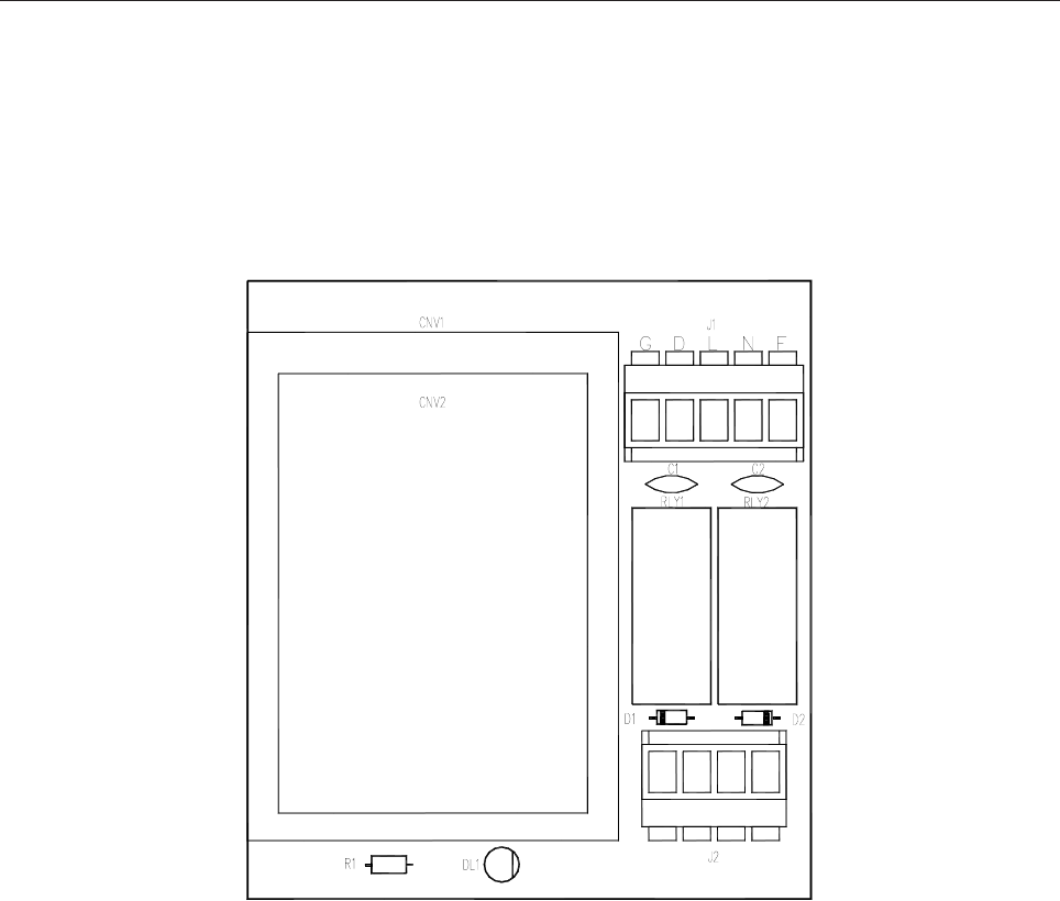
MAINS DISTRIBUTION BOARD SCH0265AR0
SCH0265AR0 Component layout
SCH0265AR0 COMPONENT LIST
Part Name/Number Description Qty. Comps.
CC 2nF2 2kV 01045A 01045A CERAMIC CAPACITOR 2 C1-2
CNV AC-DC ATC-12S E0037 AC DC CONVERTER 1 CNV1
D 1N4148 03001 03001 DIODE 2 D1-2
DL LEDG3 03053 03053 GREEN LED DIODE 3mm 1 DL1
J CON HD515V/05-4PVE 02881+02882 PANDUIT PCB CON. 1 J2
J CON HD515V/05-5PVE 02895+02896 PANDUIT PCB CON. 1 J1
R 2K7 0046 0046 RES 1/4W 5% 1 R1
RL 40.31.24 7567C RELE 2 RLY1-2
130
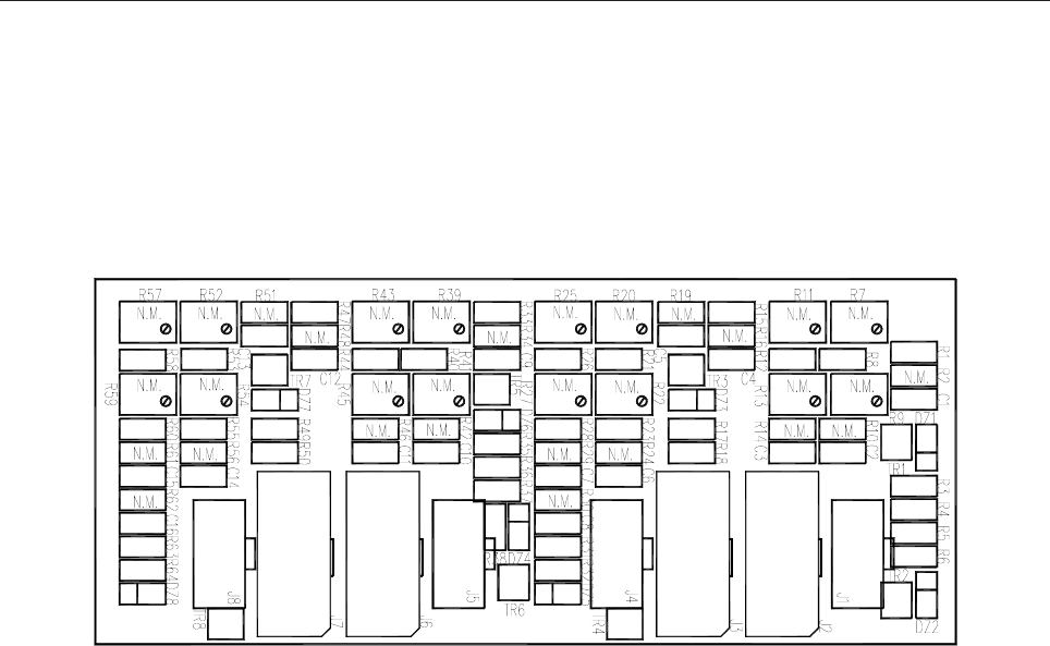
POWER SUPPLY INTERFACE BOARD SCH0288AR1
SCH0288AR1 Component layout
SCH0288AR1 COMPONENT LIST
Part Name/Number Description Qty. Comps.
CC 1nF-S 01096 01096 SMD 1206 CAPACITOR 16 C1-16
DZ 5V1-S 03128 03128 SMD ZENER DIODE 8 DZ1-8
J FC-10P 02697-02699 02697+02699 PCB CONNECTOR 4 J2-3, J6-7
J FC-10P PCB FEMALE 02706 PCB FEM. CONNECTOR 4 J1, J4-5, J8
R 0R0-S 00001 00001 RES 1/4W 5% SMD 1206 16 R1, R8, R12, R15, R21, R23, R26, R28, R33,
R40, R44, R47, R53, R55, R58, R60
R 100K-1%-S 00065B 00065B RES 1/4W 1% SMD 1206 8 R3, R6, R17, R32, R35, R38, R49, R64
R 1206 N. M. N. M. RES 1/4W 5% SMD 1206 16 R2, R10, R14, R16, R19, R24, R29-30, R34,
R42, R46, R48, R51, R56, R61-62
R 8K2-1%-S 00052B 00052B RES 1/4W 1% SMD 1206 8 R4-5, R18, R31, R36-37, R50, R63
RV 3266W N. M. N. M. VARIABLE RESISTOR 16 R7, R9, R11, R13, R20, R22, R25, R27, R39,
R41, R43, R45, R52, R54, R57, R59
TR BC847 03456 03456 NPN SMD TRANSISTOR 8 TR1-8

131
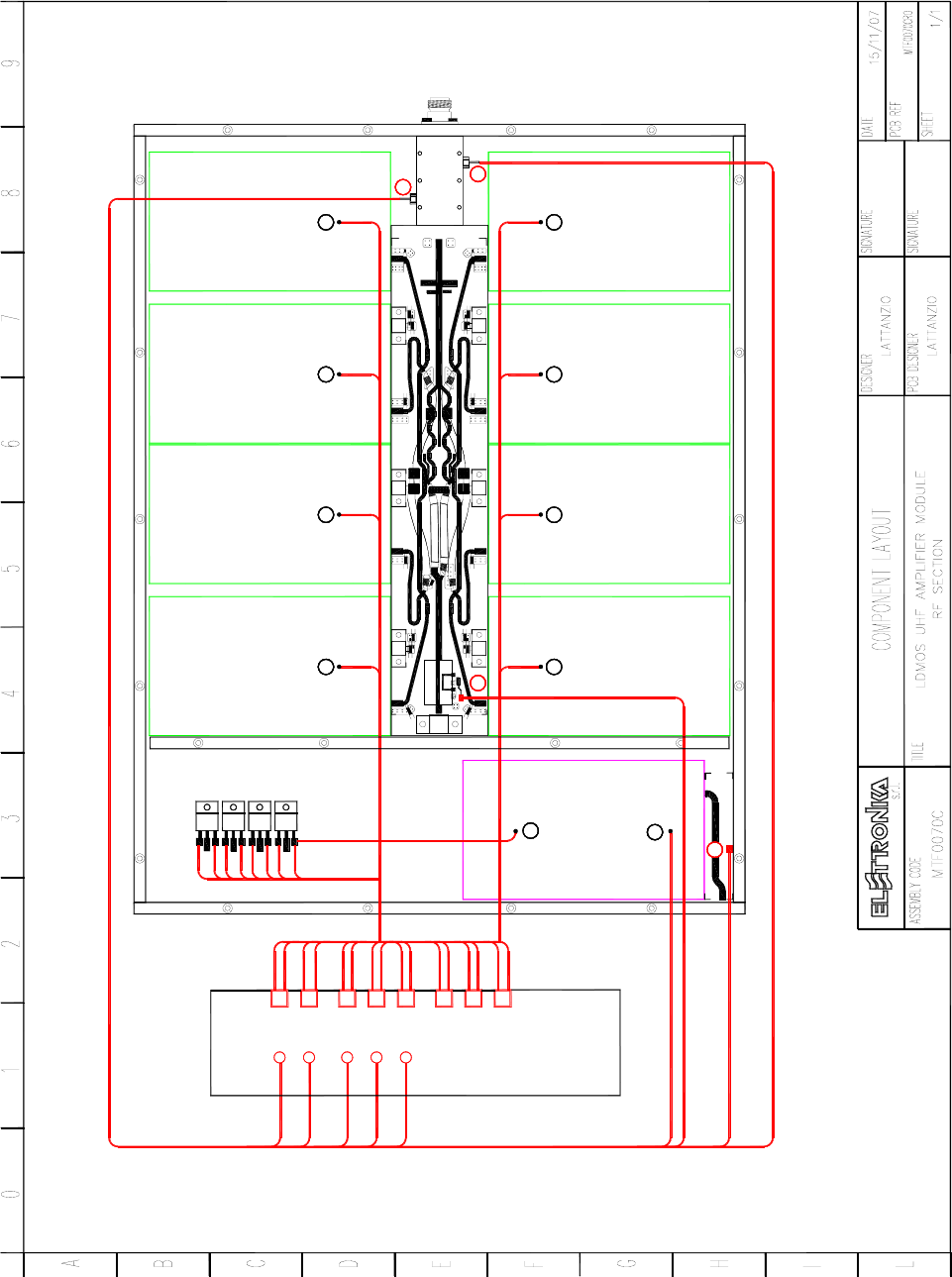
LDMOS UHF AMPLIFIER MODULE MTF0070CR0
DESCRIPTION
The MTF0070C is the RF Amplifier module of the AUTV/1500LD based on LDMOS technology. The RF
Amplifier module is composed by eight broadband amplifier boards (SCH0192A) coupled together by
means of Wilkinson combiners, driven by means another amplifier board. The module also includes the
cooling heatsink and a small Interface board (SCH0221A) which forwards power supply to the two stages,
groups the power and temperature into a single connector, more easily managed inside the transmitter. The
driver stage of the amplifier module is provided with a Gate control to inhibit the output power.
TECHNICAL CHARACTERISTICS
Frequency Range 470 - 860MHz
Output Power 1300W
Gain 23dB (±2)
Driver Stage Quiescent Current (cold) 4A (2A for each transistor to 32V)
Amplifier Stage Quiescent Current (cold) 2A (1A for each transistor to 32V)
RF Input Impedance 50Ω
RF Output Connector / Impedance 7/16” Female / 50Ω
MTF0070CR0 COMPONENT LIST
Elettronika Code Description Qty
00001 0Ω 1206 SMD RESISTOR 2
00221B 75Ω 1206 SMD RESISTOR 2
01041D 1nF 1206 SMD CERAMIC CAPACITOR 2
01400 BYPASSING CAPACITOR 13
01408 BYPASSING CAPACITOR 2
02402 7/16” FEMALE CONNECTOR 1
02512 SMA SOCKT PANEL MOUNTING 1
03017 MBR3045PT DIODE 4
03207 HSMS2802 DIODE 2
08502 RG 316 50Ω CABLE 3.00
08527 HF-85 ENDIFORM CABLE 0.20
PN0998A PN0998AR1 BIAS ADDER PCB 2
PN1091A PN1091AR3 UHF DIRECTIONAL COUPLER PCB 1
SCH0192AR0 200W LDMOS UHF AMPLIFIER MODULE 9
SCH0221AR0 AMPLIFIER INTERFACE BOARD 1
SCH0248AR0 8 INPUTS WILKINSON PCB 1
SCH0249AR0 4 WAY WILKINSON PCB 1
SCH0250AR0 4 WAY WILKINSON PCB 1
SCH0251AR0 2 WAY WILKINSON PCB 1
SCH0252AR0 UHF INPUT COUPLER 1
132
FWD
RF OUTPUT
SCH0221A
GATE
TEMP
REF
FWD
RF OUTRF IN
GATE
RF IN 3 RF OUT 3
RF IN 1 RF OUT 1
RF IN 2 RF OUT 2
CONTROL BOARD
TEMPERATURE
SENSOR
GATE TEMP REF FWD RS232 SOCKET
RS485 SOCKET
TLM SOCKET
AGC SOCKET
LCD DISPLAY
To AMPLIFIER CONTROL
SCH0223A
(SCH0192A)
INTERFACE BOARD
FWD
RF INPUT
2 WAY WILKINSON DIVIDER
4 WAY WILKINSON DIVIDER
SCH0192ARF IN 4 RF OUT 4
SCH0192A
SCH0192A
SCH0192A
RF IN 7 RF OUT 7
RF IN 5 RF OUT 5
RF IN 6 RF OUT 6
SCH0192ARF IN 8 RF OUT 8
8 WAY WILKINSON COMBINER
MONITOR
SCH0192A
SCH0192A
DRIVER
SCH0192A
REF
4 WAY WILKINSON DIVIDER
133
SCH0221A
J14
GATE
J12
FWD
J13
REF
TP1 TP2
UNB1
J15 J16
UNB2
RF
FLORIDA
32-1037
RF
FLORIDA
32-1037
RF
FLORIDA
32-1123
PN1089A
RF
FLORIDA
32-1037
RF
FLORIDA
32-1037
PN1010A
RF
FLORIDA
32-1037
RF
FLORIDA
32-1037
T11
T22
T44
T33
T77
T88
T66
T55
T99
T1
T11
T2
T22
T3
T33
T4
T44
T5
T55
T66
T6
T7
T77
T8
T88
T12
T13
T14
T15
T16
T15
PN1083A
TP3 TP4 TP5 TP6 TP7 TP8
T99 T14
T14
T8
T7
T6
T5
T4
T3
T2
T1
SCH0192A
RF AMPLIFIER BOARD #1
SCH0192A
RF AMPLIFIER BOARD #2
SCH0192A
RF AMPLIFIER BOARD #3
SCH0192A
RF AMPLIFIER BOARD #4
SCH0192A
RF AMPLIFIER BOARD #5
SCH0192A
RF AMPLIFIER BOARD #6
SCH0192A
RF AMPLIFIER BOARD #7
SCH0192A
RF AMPLIFIER BOARD #8
SCH0192A
DRIVER MODULE
T12
T13
82Ω
1nF
HSMS 2802
AMPLIFIER INTERFACE BOARD
PN1091A
DIRECTIONAL COUPLER
134
LDMOS AMPLIFIER MODULE SCH0192AR0
DESCRIPTION
The RF module is an integrated TV linear amplifier designed for UHF band, this module employs push-pull
LDMOS technology in order to achieve very good efficiency, high linearity and reliability.
LDMOS transistors operate in AB class. It is a wideband amplifier over the full frequency, no adjustment is
required for the channel change. The board includes RF section amplifier, bias circuit, protection circuit and
matching networks. A silver plated copper plate is brazed with PCB in order to obtain low thermal resistance.
Providing a minimum of 200W Pk sync linear power, this module is the perfect amplifier for any broadband
UHF power transmitter.
TECHNICAL CHARACTERISTICS
Frequency Range 470 - 860MHz
Output Power 200W PEP
Gain 14dB (±1)
Output LDMOS Power Supply 32V (±2%)
Output LDMOS Bias Current @ +32V Vdd 1A
RF Input Impedance 50Ω
RF Output Impedance 50Ω
Curve response graphic
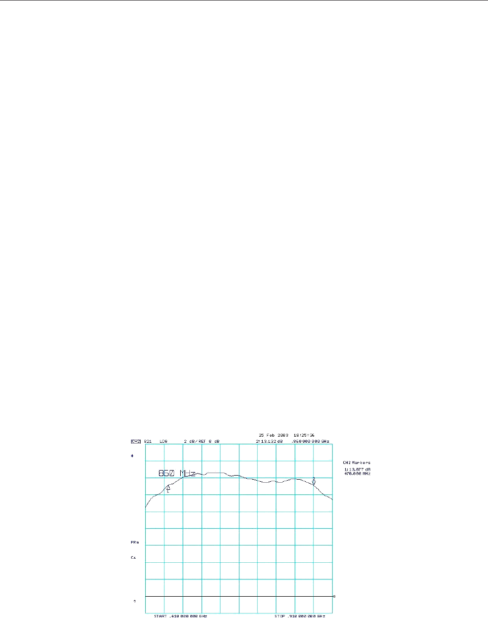
Middle frequency 660MHz, span 500MHz, 2dB/div., reference to the arrow

135
CALIBRATION PROCEDURE
- Technical characteristics
Power supply voltage 32V (± 2%)
Polarisation current 1.0 cold for each device (2A total), ± 0.1A
Gain for low signal Not less than 13dB in the 470-860MHz band (± 1dB)
Compare to the typical curve eclosed
- Adjustment procedure
Polarisation current calibration 32V stabilised power supply
10A amperometer
Gain curve Network analyser
- Adjustment points description
R7-R8 (Trimmers) Adjust the current absorbed in stand-by (1.0A per device)
- Calibration steps
STEP 1: Close the input and the output of the module by connecting them to a 50ΩΩ
ΩΩ
Ω dummy load and
connect the spectrum analyser through a directive sample, in order to look for self-oscillation of the module,
if any (anyway the module has been designed so that it would not self-oscillate even if totally de-coupled,
without any input or output load).
STEP 2: Check the voltages of the polarisation circuits without assembling the transistors first:
connect the 32V power supply to the proper turret by means of a fastening screw, then give power and check data:
- the stabilised voltage on the zener diodes DZ1 and DZ2 is about 15V compared to the ground;
- the stabilised voltage on the zener diodes DZ3 and DZ4 is about 6.8V compared to the ground;
- the voltage on the pads to which the gates of the LDMOS transistors will be soldered (R23 and R24 resi-
stors side) changes from 0V to a maximum value of about 6V when moving the relevant trimmer (R7-R8).
STEP3: Check the work of the protections.
- Set both trimmers so that there is a value of about 4.5V on the pads of the gates;
- solder some wire to the pad between the two LEDs, next to the serigraphy of the input hybrid H1;
- in order to check the work of the protections aboard, a power of about 4V has to be supplied to the wire,
for example by touching with it the reophore of C23 or C24 which is not connected to ground; the two red
LEDs will immediately light up and the two RF transistors will be switched off at the same time: the polarisation
current (2A) will decrease to 0 and of course the gain curve displayed by the spectrum analyser will decrease;
- after this it is important to restore the position of the two trimmers for the minimum voltage! Then
disconnect the 32V power supply.
136
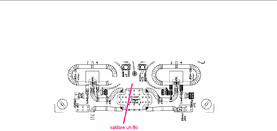
Solder a wire
STEP 4: Fastening of the LDMOS transistors: after properly cleaning the plate surface, smear a thin layer
of silicone fat on the lower side of the flange of the MOSFETs, fasten them to the heat sink and solder the gate
first, then the drain. Solder the two 13pF (ATC) chip capacitors and above them the two 1-5pF capacitive
trimmers, between the two pair of gates, as shown by the mounting plan.
STEP 5: Connect serially a c.c. amperometer to the power supply, with scale starting from more than 5A (i.e. 10A).
STEP 6: Power the module and check the MOSFET is not absorbing current; this means that the device is
integral and working correctly.
STEP 7: Slowly turn the R7 trimmer until the MOSFET absorbs 1A, always checking that there are no self-oscillation; under
this conditions it is possible to check by means of a digital tester that the voltage on the gate is about 5.2-5.4V.
STEP 8: Repeat the previous step for the other section of the module, this time turnign R8 and checking that the indication of
the current on the amperometer increases to 2A total (which includes the current of the other device left on).
STEP 9: Check the response curve of the module by means of the network analyser.
STEP 10: Check the response curve for low signal with centre 660MHz and span 500MHz, 2dB/div.
STEP 11: The curve should be similar to the one enclosed, with a tolerance of ± 0.5dB. To obtain this, act on
the four trimmers C41-C41a and C42-C42a with the proper “calibrator”, inorder to flatten the curve as much
as possible, especially at the edged of the band which represents the minimum values.
STEP 12: Finally, check that the current in stand-by does not increase by more than 15÷20%, reaching at
worst 2.3÷2.4A when the heat sink is hot and not ventilated.
Note: when mounting-removing the PALLET on the heat sink, tightly fasten the screw of each all “N” input and output
connectors. These are mounted with a single 3mm screw and if it is not properly fastened it may be detached from the PCB
by a movement of the connector once it has already been soldered to the path.
137
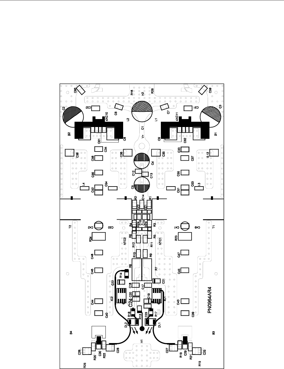
SCH0192AR0 LDMOS UHF Amplifier Board Component layout

138
SCH0192AR0 COMPONENT LIST
Elettronika Code Description Manufacturer, Mfr. Code Qty Comps.
00045A 2K2 1206 5% 1/4W RESISTOR PHICOMP, RC1206JR072K2L 4 R1-4
00042A 1K2 1206 1% 1/4W RESISTOR PHICOMP, RC1206FR071K2L 4 R5-6, R9-10
00800 50K 3.8" SQUARE TRIMMER BOURNS, 3296W-1-503 2 R7-8
00056B 18K 1206 5% 1/4W RESISTOR PHICOMP, RC1206JR0718KL 2 R11-12
00075A 680K 1206 5% 1/4W RESISTOR PHICOMP, RC1206JR07680KL 1 R13
00001 0R 1206 RESISTOR PHICOMP, RC1206JR070RL 1 R14
00432 50 OHM 60W TERMINATION DICONEX, 17-0185 2 R25-26
00049A 4K7 1206 1% 1/4W RESISTOR PHICOMP, RC1206FR074K7L 2 R17-18
00012A 3R9 1206 5% 1/4W RESISTOR PHICOMP, RC1206JR073R9L 4 R19-22
00396 1K0 2512 5% 1W RESISTOR TYCO, 35201K0JT 2 R23-24
01807B 470uF 50V ELECTROLITIC CAPACITOR ADIMPEX, CL514750 3 C1-3
01795 100uF PTH 50V ELET. VERT. CAPACIT. ADIMPEX, CL211050 2 C4-5
01145 1nF 50V PORCELAIN CAPACITOR ATC, ATC100B102JT50XT 6 C6-7, C25-28
01065H 100nF 2220 1kV CERAMIC CAPACITOR SYFER, 2220J1K00104KXT 4 C8-9
01135 100pF 500V PORCELAIN CAPACITOR ATC, ATC100B101KT500XT 8 C10-11
01065G 100nF 1210 250V CAPACITOR SYFER, 1210J2500104KXT 9 C12-14, C21-24
01613A 1uF SMD 35V TANTALUM CAPACITOR NIC COMPONENTS CORP.,
NTC-T105M35TRB 2 C15-16
01626A 10uF SMD 16V TANT. CAPACITOR KEMET, KEMT491C106K016AT 2 C19-20
01123 20pF 500V PORCELAIN CAPACITOR ATC, ATC100B200JT500XT 4 C29-32
01104 1.3pF 500V PORCELAIN CAPACITOR ATC, ATC100B1R3DT500XT 2 C33-34
01143 470pF 200V PORCELAIN CAPACITOR ATC, ATC100B471KW200X 4 C35-38
01108 4.7pF 500V PORCELAIN CAPACITOR ATC, ATC100B4R7DT500XT 2 C57-58
01117 10pF 500V PORCELAIN CAPACITOR ATC, ATC100B100JT500XT 2 C55-56
01104B 3.6pF 500V PORCELAIN CAPACITOR ATC, ATC100B3R6DT500XT 2 C43-44
01119A 13pF 500V PORCELAIN CAPACITOR ATC, ATC100B130KT500XT 2 C49-50
01113 8.2pF 500V PORCELAIN CAPACITOR ATC, ATC100B8R2JT500XT 4 C51-54
01160 0.3pF 500V PORCELAIN CAPACITOR ATC, ATC100B0R3CT500XT 1 C60
01485 VARIABLE CAPACITOR 1-5pF JOHANSON, 9702-1 2 C41-42
04034 LDMOS TRANSISTOR BLF861 PHILIPS, BLF861/A 2 T1-2
00661 NTC THERMISTOR 100K VISHAY, 238164063104 2 NTC1-2
04583 IC SPDT ANALOG SWITCH MAXIM, DG419DY-E3 2 IC1-2
03135 DIODE 15V ZENER FAIRCHILD, MMSZ5245B 2 DZ1-2
03137 DIODE 6.8V ZENER DIOTEC, GSEZMM6.8/D2 2 DZ3-4
03056 LED RED SMD KINGBRIGHT, KA3528EC 2 DL1-2
07684 SILVERED WIRE 1.2MM ELETTRONIKA, 07684 0.25 L1-2
DET0643K 200W LDMOS PALLET ELETTRONIKA, DET0643K 1
01111 6.8pF 500V PORCELAIN CAPACITOR ATC, ATC100B6R8KT500XT 4 C45-48
V0774 SPACER 3X10 F/F ELEKTROZUBEHOR,
DD10H305010 1
08491 PRE-FOLDED CABLE EZ FORM CABLE, EZ9025 2 B1-2
08492 PRE-FOLDED CABLE EZ FORM CABLE, EZ3425 SILVER 2 B3-4
01109 5.6pF 500V PORCELAIN CAPACITOR ATC, ATC100B5R6DT500XT 2 C39-40
01077A 1uF PTH 100V POLYESTER CAPACITOR ARCOTRONICS, R82EC4100DQ70J2 C61-62
139
SCH0221AR0 Component layout
SCH0221AR0 COMPONENT LIST
Part Name/Number Description Qty. Comps.
CC 100nFAVX 01065A 01065A CERAMIC CAPACITOR 4 C1, C3, C6, C8
CE 100uF100V 01795B ELET. CAPACITOR 1 C2
CE 100uF50V 01795 01795 ELET. CAPACITOR 1 C7
CE 10uF35V-S 01778A 01778A ELET. SMD CAPACITOR 2 C4-5
D 1N4007 03009 03009 DIODE 1 D4
D 6CWQ10FN 03026 2x3.5A SMD DIODE SCHOT. 3 D1-3
IC LM317HV 04340A INTEG CIRCUIT 2 IC1-2
J FC-16P 02701-02700 02701+02700 PCB CONNECTOR 1 J21
J SCREWCONN2 02853 02853 PCB SCREW CONNECTOR 2 J11, J19
J SCREWCONN3 02860 02860 PCB SCREW CONNECTOR 1 J20
J TESTP1.3mm 07913 07913 TEST POINT 17 J1-10, J12-18
JU JUMP2 02739-02742 02739+02742 PAN2 MALE 3 JP1-2, JP4
JU JUMP3 02707-02742 02707+02742 PAN3 MALE 1 JP3
R 0R33-1W-S 00380 RES 1W 5% SMD 2512 2 R1-2
R 100K-S 00065A 00065A RES 1/4W 5% SMD 1206 1 R7
R 220R-S 00033A 00033A RES 1/4W 5% SMD 1206 1 R4
R 22K-S 00057A 00057A RES 1/4W 5% SMD 1206 1 R5
R 270R-S 00034A 00034A RES 1/4W5% SMD 1206 1 R3
R 4K7-S 00049A 00049A RES 1/4W 5% SMD 1206 1 R6
TR BC856 03455 03455 PNP SMD TRANSISTOR 1 TR1
AMPLIFIER INTERFACE BOARD SCH0221AR0
140
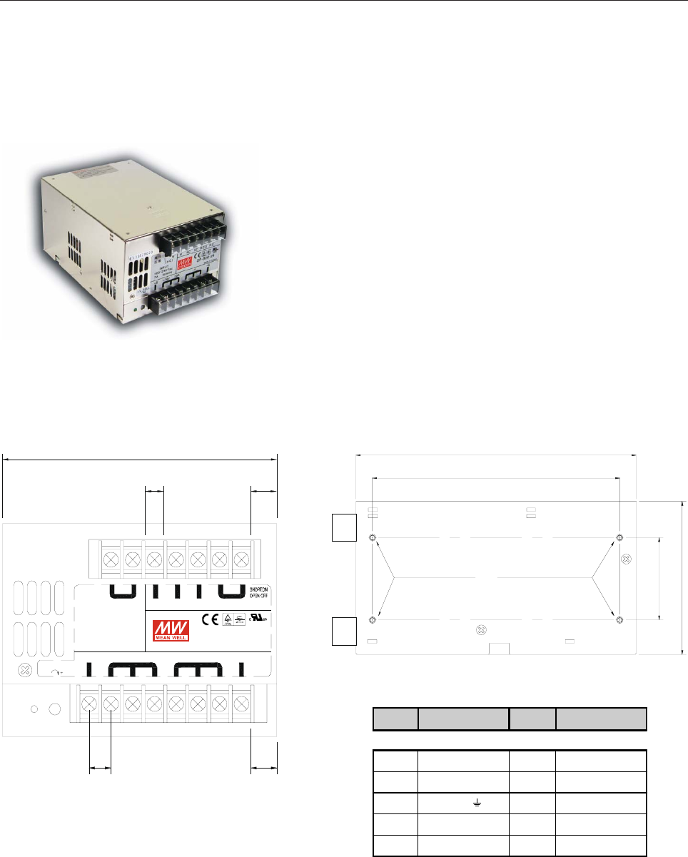
SP500-27/48 DE2 SWITCHING POWER SUPPLY E0012 - E0013
MAIN FEATURES
- Universal AC input / Full range
- Built-in active PFC function, PF>0.95
- Protections: Short circuit / Over load / Over voltage / Over temp.
- Forced air cooling by built-in DC fan
- Built-in cooling Fan ON-OFF control
- Built-in remote sense function
- Fixed switching frequency at 110kHz
MECHANICAL SPECIFICATION
170
150
50
93
2-M3 L=16mm max.2-M3 L=4mm max.
9.5 11.5
811.5
120
15141312111098
7654321
7A 50/60Hz
100-240VAC
INPUT
(AC )
-S-V+24V 20A+S
+VADJ.
SP-500-24
E183223
LEVEL5
R.C.G.L N FG NC NC R.C.
PIN N° ASSIGNMENT PIN N° ASSIGNMENT
1 AC/L 7 R.C.
2AC/N8 +S
3 FG 9 ~ 11 DC OUTPUT +V
4, 5 NC 12 ~ 14 DC OUTPUT -V
6R.C.G.15 -S
141
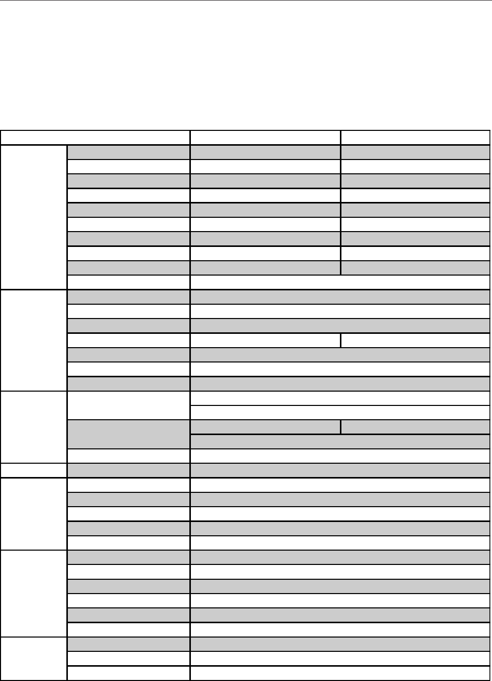
TECHNICAL CHARACTERISTICS
MODEL SP500-27 SP500-48
OUTPUT
DC VOLTAGE 27V 48V
RATED CURRENT 18A 10A
CURRENT RANGE 0 ~ 18A 0 ~ 10A
RATED POWER 486W 480W
RIPPLE & NOISE (max.) Note 2 200mVp-p 300mVp-p
VOLTAGE ADJ. RANGE 24 ~ 30V 41 ~ 56V
VOLTAGE TOLERANCE Note 3 ± 1.0% ± 1.0%
LINE REGULATION ± 0.5% ± 0.5%
LOAD REGULATION ± 0.5% ± 0.5%
SETUP, RISE, HOLD TIME 1500ms, 50ms, 20ms at full load
INPUT
VOLTAGE RANGE 88 ~ 264VAC 124 ~ 370VDC
FREQUENCY RANGE 47 ~ 63Hz
POWER FACTOR PF>0.95/230VAC PF>0.95/115VAC at full load
EFFICIENCY (Typ.) 86.5% 87%
AC CURRENT 7A/115VAC 3.5/230VAC
INRUSH CURRENT (Max.) 18A/115VAC 36A/230VAC
LEAKAGE CURRENT <3.5A/240VAC
PROTECTION
OVER LOAD 105 ~ 135% rated output power
Protection type: Fold back current limiting, recovers automatically after fault condition is removed
OVER VOLTAGE 31 ~ 36.5V 57.6 ~ 67.2V
Protection type: Hiccup mode, recovers automatically after fault condition is removed
FAN CONTROL O.T.P. RTH1 or RTH2 >= 50°C FAN ON, <= 45°C FAN OFF, >= 70°C output shutdown
FUNCTION REMOTE CONTROL RC+/RC-: Short = power on; Open = power off
ENVIRONMENT
WORKING TEMP. -10 ~ +50°C (Refer to output load derating curve)
WORKING HUMIDITY 20 ~ 90% RH non-condensing
STORAGE TEMP., HUMIDITY -20 ~ +85°C, 10 ~ 95% RH
TEMP. COEFFICIENT ± 0.03%/°C (0 ~ 50°C)
VIBRATION 10 ~ 500Hz, 2G 10min./1cycle, period for 60min. each along X, Y, Z axes
SAFETY & EMC
(Note 4)
SAFETY STANDARDS UL1950, TUV EN60950 Approved
WITHSTAND VOLTAGE I/P-O/P:3KVAC I/P-FG:1.5KVAC O/P-FG:0.5KVAC
ISOLATION RESISTANCE I/P-O/P, I/P-FG, O/P-GD:100M Ohms/500VDC
EMI CONDUCTION & RADIATION Compliance to EN55022 (CISPR22) Class B
HARMONIC CURRENT Compliance to EN61000-3-2,-3
EMS IMMUNITY Compliance to EN61000-4-2,3,4,5,6,8,11; ENV50204, Light industry level, criteria A
OTHERS
MTBF 133.4K hrs min. MIL-HDBK-217F (25°C)
DIMENSION 170*120*93mm (L*W*H)
PACKING 1.9kg; 8pcs/15.2kg/1.06CUFT