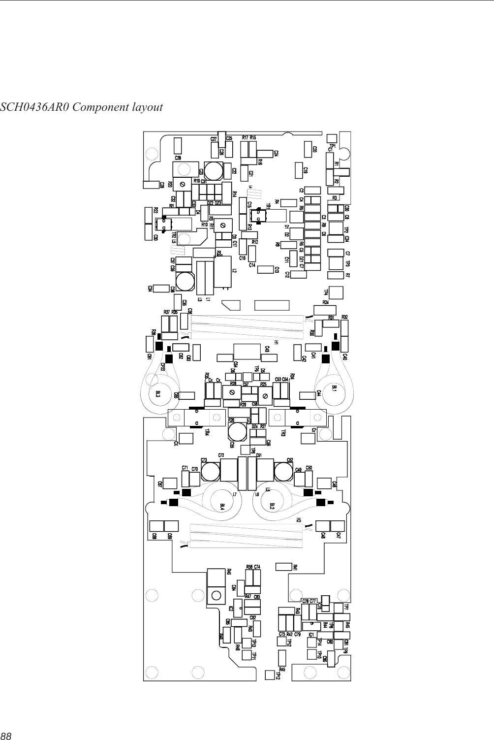
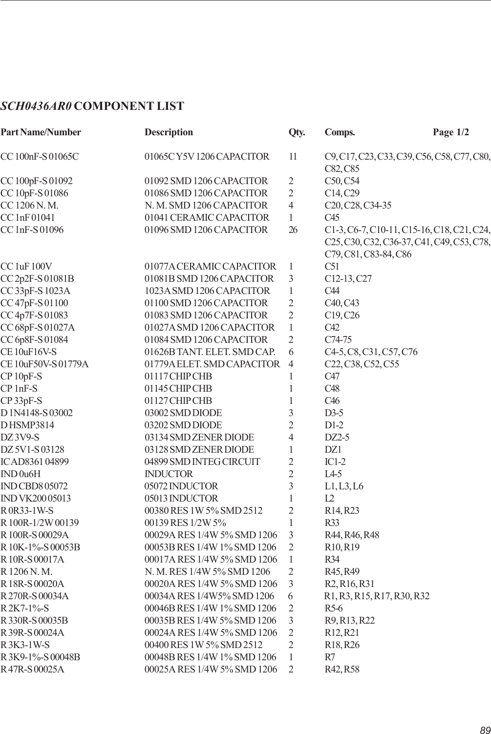
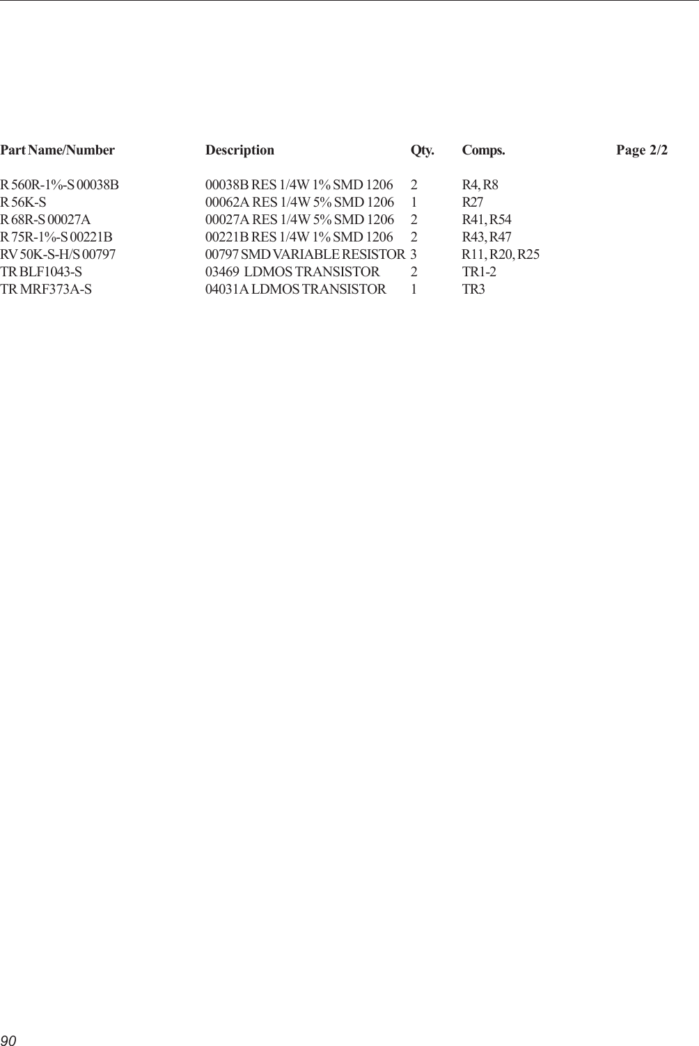
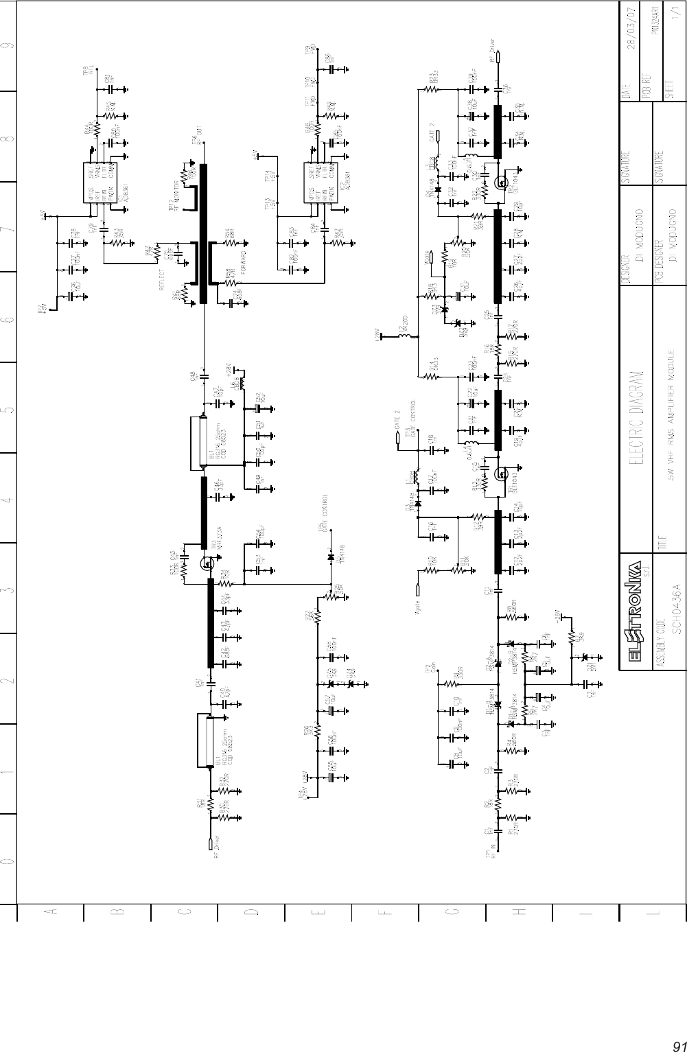
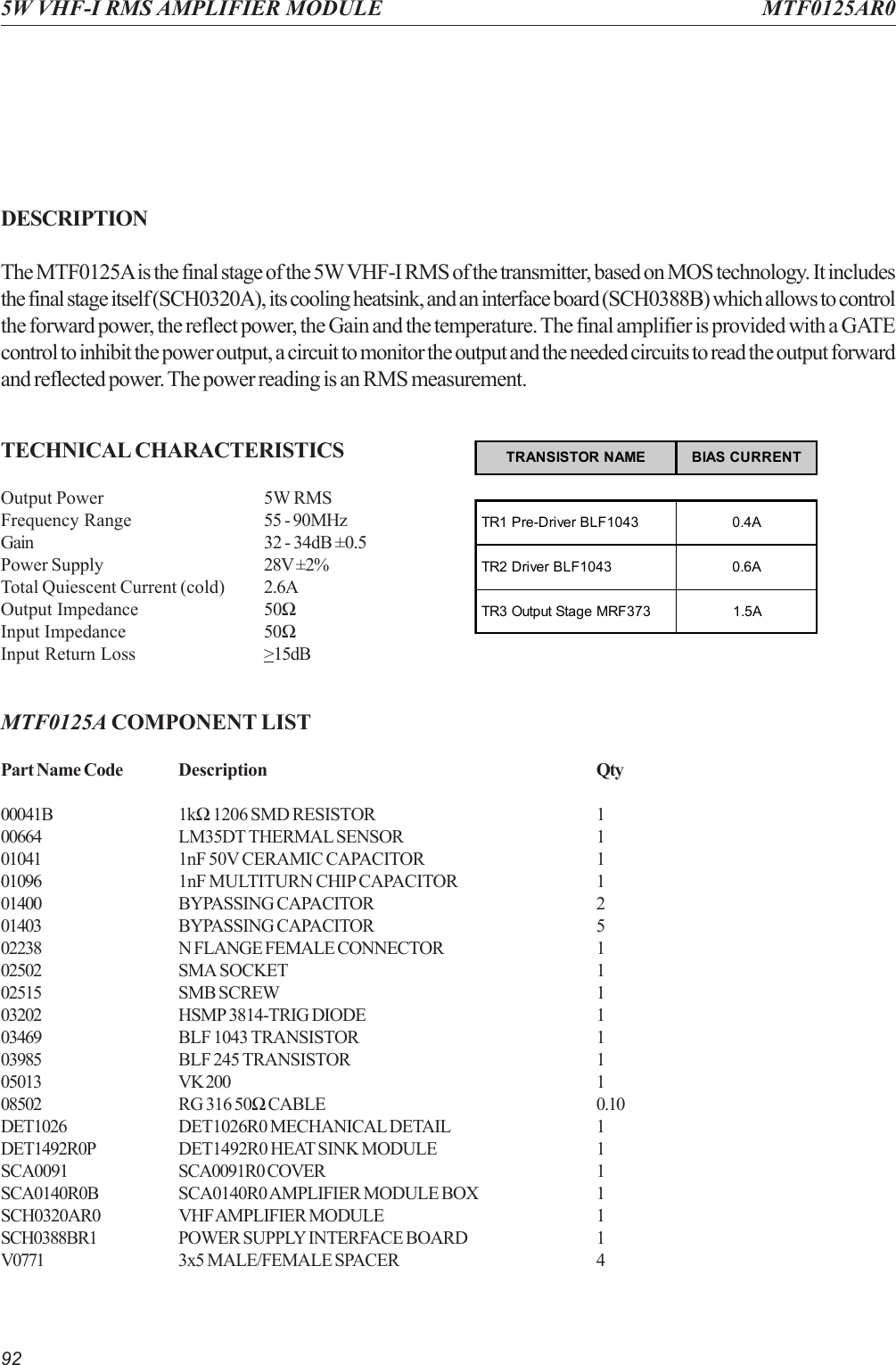
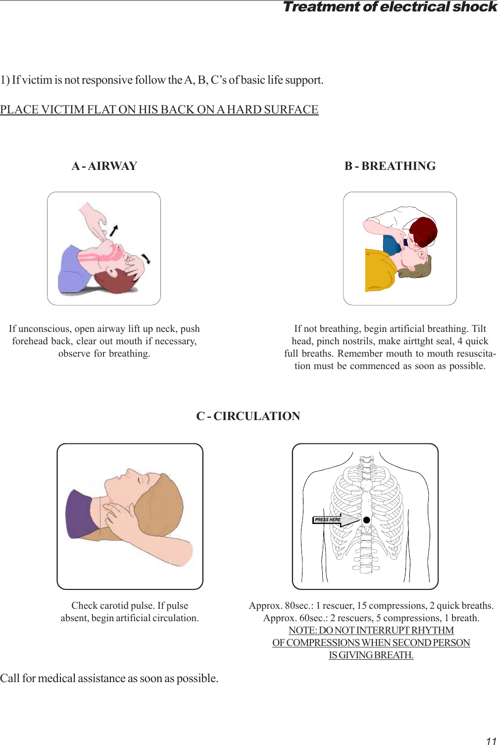
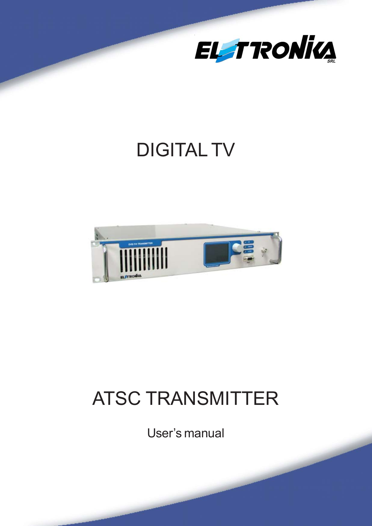
Elettronika S r l TXUD500 500 Watt DTV Transmitter User Manual Part One

Elettronika S.r.l. 500 Watt DTV Transmitter Part One

User Manual Part One

ATSC TRANSMITTERDigital TVCODE APD043AAPD047AAPD045ATITLE ATSC TRANSMITTER REV       0DATE 20/02/08
SS 96   Km 11370027 Palo del Colle (Ba) ITALYTel. +39 (0)80 626755Fax +39 (0)80 629262E-mail: elettronika@elettronika.itWeb site: http://www.elettronika.itRegistration number: IT-17686Registration number: IT-24436ATSC Transmitter FamilyCODE MODELAPD043A ATSC UHF TRANSMITTERAPD047A ATSC VHF-III TRANSMITTERAPD045A ATSC VHF-I TRANSMITTER
ATSC Transmitter Family .................................................................................................. 2Summaries ......................................................................................................................... 3Warning .............................................................................................................................. 7Warranty ............................................................................................................................. 8Introduction ....................................................................................................................... 9Content of the manual ...................................................................................................... 9Treatment of electrical shock ......................................................................................... 11First-aid ......................................................................................................................... 12    Treatment of electrical burns ......................................................................................... 12    Note ............................................................................................................................... 12RoHS Normative .............................................................................................................. 13ATSC TRANSMITTER ...................................................................................................... 15Section 1 - Information ................................................................................................... 17    1.1 Description .............................................................................................................. 18    1.2 Main Features ......................................................................................................... 18    1.3 Technical Characteristics......................................................................................... 19    Front panel .................................................................................................................... 20    Rear panel ..................................................................................................................... 21    Block Diagram ...............................................................................................................22    1.4 Operational Details .................................................................................................. 23        1.4.1 TS Input Management ...................................................................................... 23            - Redundancy management .................................................................................. 23            - Reed Solomon FEC ............................................................................................ 24            - Bit rate adaptation ...............................................................................................24            - Squelch ............................................................................................................... 24        1.4.2 Synchronization and Clocks ............................................................................. 24        1.4.3 Output Signal ................................................................................................... 25        1.4.4 Non-Linear Precorrection ................................................................................. 25        1.4.5 Linear Precorrection ......................................................................................... 25        1.4.6 Control of the equipment .................................................................................. 26        1.4.7 Test Modes ....................................................................................................... 26        1.4.8 Power Handling ................................................................................................ 26        1.4.9 Alarms and Automation .................................................................................... 27        1.4.10 AGC: Implementation and Details .................................................................. 29        ATSC TRANSMITTER AGC Cable ............................................................................ 31        1.4.11 Log ................................................................................................................. 32Section 2 - Installation .................................................................................................... 33    2.1 Operating Environment ........................................................................................... 34Summaries
    2.2 First Installation ....................................................................................................... 34    2.3 ATSC TRANSMITTER with GPS Clock Source ...................................................... 35    2.4 ATSC TRANSMITTER remote control with Elettronika RCU ................................... 35    2.5 ATSC TRANSMITTER with PC ............................................................................... 36Section 3 - Operation ...................................................................................................... 37    3.1 Local Control ...........................................................................................................38    3.2 LEDs ....................................................................................................................... 38    3.3 Menu Management ................................................................................................. 39        3.3.1 Title Bar ............................................................................................................ 39        3.3.2 Status Bar ......................................................................................................... 39        3.3.3 Diagram Screen ............................................................................................... 40        3.3.4 Browsing the menus and parameters ............................................................... 41        3.3.5 Composition of a menu .................................................................................... 42    3.4 Parameters and menu description .......................................................................... 44        3.4.1 Input Menu ....................................................................................................... 44            - Configuration Submenu ...................................................................................... 44            - Stream1 Errors Submenu .................................................................................... 46            - Stream2 Errors Submenu .................................................................................... 46        3.4.2 Modulation Menu .............................................................................................. 47        3.4.3 RF Menu...........................................................................................................48            - Frequency Submenu ........................................................................................... 49            - Power Submenu.................................................................................................. 50            - Amplifier Submenu .............................................................................................. 52            - Output Submenu ................................................................................................. 53            - Precorrection Submenu ...................................................................................... 54        3.4.4 Setup Menu ...................................................................................................... 55            - Control Submenu ................................................................................................ 56            - Display Submenu ................................................................................................ 57            - Clock Submenu .................................................................................................. .57            - Power Supply Submenu...................................................................................... 58            - Versions Submenu .............................................................................................. 58    3.5 Log Screen ..............................................................................................................59    3.6 Alarm Screen ........................................................................................................... 59    3.7 Firmware Upgrade................................................................................................... 59    ATSC TRANSMITTER Menu Map ................................................................................. 61Section 4 - Diagram ......................................................................................................... 63    - APD043A ATSC TRANSMITTER Cable Diagram ....................................................... 64    - APD047A ATSC TRANSMITTER Cable Diagram ....................................................... 65
    - APD045A ATSC TRANSMITTER Cable Diagram ....................................................... 66    - APD043A_APD047A_APD045A ATSC TRANSMITTER Component list .................... 67    - SCH0135A Control Board and Display ....................................................................... 69        - Description .............................................................................................................. 69            - Dip-switch............................................................................................................ 69        - Technical Characteristics ........................................................................................ 69    - SCH0135A Top layer Component layout..................................................................... 70    - SCH0135A Bottom layer Component layout ............................................................... 71    - SCH0135A Component list ......................................................................................... 72    - SCH0135A Electric Diagram ....................................................................................... 74    - A1592 ATSC UHF Modulator Module .......................................................................... 77        - Description .............................................................................................................. 77        - Main Features .........................................................................................................77        - Connectors .............................................................................................................. 77    - A1703 ATSC VHF-I/III Modulator Module .................................................................... 78        - Description .............................................................................................................. 78        - Main Features .........................................................................................................78        - Connectors .............................................................................................................. 78    - MTF0116A 5W UHF RMS Amplifier Module ................................................................ 79        - Description .............................................................................................................. 79        - Technical Characteristics ........................................................................................ 79        - MTF0116A Component list ...................................................................................... 79        - MTF0116A Component layout ................................................................................. 80        - SCH0417A Component layout ................................................................................ 81        - SCH0417A Component list ..................................................................................... 82        - SCH0417A Electric Diagram ................................................................................... 83    - MTF0118A 5W VHF-I/III RMS Amplifier Module.......................................................... 86        - Description .............................................................................................................. 86        - Technical Characteristics ........................................................................................ 86        - MTF0118A Component list ...................................................................................... 86        - MTF0118A Component layout ................................................................................. 87        - SCH0436A Component layout ................................................................................ 88        - SCH0436A Component list ..................................................................................... 89        - SCH0436A Electric Diagram ................................................................................... 91    - MTF0125A 5W VHF-I RMS Amplifier Module ............................................................. 92        - Description .............................................................................................................. 92        - Technical Characteristics ........................................................................................ 92        - MTF0125A Component list...................................................................................... 92
        - MTF0125A Component layout ................................................................................ 93        - SCH0320A Component layout ................................................................................ 94        - SCH0320A Component list ..................................................................................... 95        - SCH0320A Electric Diagram ................................................................................... 96    - SCH0388B Power Supply Interface Board ................................................................. 97        - SCH0388B Power Supply Interface Board Component layout ............................... 97        - SCH0388B Component list ..................................................................................... 98        - SCH0388B Electric Diagram ................................................................................... 99    - E0064 SP-320-27/48 Switching power supply .......................................................... 100        - Main Features ....................................................................................................... 100        - Mechanical Specifications ..................................................................................... 100        - Technical Characteristics ...................................................................................... 101
7WARNINGThe apparatus described in this manual has been designed and manufactured with devices to safe-guard the users. In any case it is recommended that during any operation of installation, maintenance,miscellaneous interventions and calibrations requiring the apparatus to be switched on,THE USER TAKES ALL THEPRECAUTIONS AGAINST INCIDENTSIt is required to use the proper clothes and protection gloves in order to prevent damages from inci-dental contacts with high-voltage parts.The manufacturer declines every responsibility in case the recommendations above are not followed.IMPORTANTThe component lists attached to the relevant electrical diagrams indicate for each item the reference,the description and the type normally used.The  Elettronika S.r.l. though reserves the right to use or supply as spare parts components withequivalent characteristics but of a different type, assuring anyway the optimal work of the apparatusin accordance with the specifications.The enclosed monographs are solely owned by Elettronika S.r.l.The use of anything enclosed in this technical manual without explicit authorization given by ElettronikaS.r.l. will be prosecuted by the law.The data and technical characteristics of the apparatus described in this manual are not compelling forthe manufacturer.The Elettronika S.r.l. reserves the right to make, without previous notice, modifications or updates inorder to improve the quality of the product.The general conditions of supply and sale are described in the contracts.The delivery time are in accordance with the products and quantities ordered.
8Summary of warrantyWe, ELETTRONIKA S.r.l., SS096  Km 113 Z.I.  PALO DEL COLLE (BA) ITALY, warrant to the ORIGINAL PURCHASER of a NEW  product, for aperiod of one (1) year from the date of purchase by the original purchaser (the “warranty period”) that the new ELETTRONIKA product is free of defectsin materials and workmanship and will meet or exceed all advertised specifications for such a product. This warranty does not extend to any subsequentpurchaser or user, and automatically terminates upon sale or other disposition of our product.Items excluded from this ELETTRONIKA warrantyWe are not responsible for product failure caused by misuse, accident, or neglect. This warranty does not extend to any product on which the serialnumber has been defaced, altered, or removed. It does not cover damage to loads or any other products or accessories resulting from ELETTRONIKAproduct failure. It does not cover defects or damage caused by use of unauthorized modificstions, accessories, parts, or service.What we will doWe will remedy any defect, in material or workmanship (except as excluded), in our sole discretion, by repair, replacement, or refund. If a refund iselected, then you must make the defective or malfunctioning component available to us free and clear of all liens or other encumbrances. The refund willbe equal to the actual purchase price, not including interest, insurance, closing costs, and other finance charges less a reasonable depreciation on theproduct from the date of original purchase. Warranty work can only be performed at our authorized service centers or at our factory. Expenses inremedying the defect will be borne by ELETTRONIKA, including one-way surface freight shipping costs within the United States. (Purchaser must bearthe expense of shipping the product between any foreign country and the port of entry in the United States and all taxes, duties, and other custom’s fee(s)for such foreign shipments).How to obtain warranty serviceYou must notify us of your need for warranty service not later than ninety (90) days after the expiration of the warranty period. We will give you anauthorization to return the product for service. All components must be shipped in a factory pack or equivalent which, if needed, mayDesclaimer of consequential and incidental damagesYou are  not entitled to recover from us any consequential or incidental damages resulting from any defect in our product. This includes any damageto another product or products resulting from such a defect.Warranty alterationsNo person has the authority to enlarge, or modify this warranty. The warranty is not extended by the lenght of time for which you are deprived ofthe use of the product. Repairs and replacement parts are provided under the terms of this warranty shall carry only the unexpired portion of thiswarranty.Design changesWe reserve the right to change the design of any product from time to time without notice and with no obligation to make corresponding changes inproducts previously manufactured.Legal remedies of purchaserThere is no warranty which extends beyond the terms hereof. This written warranty is given in lieu of any oral or implied warranties not containedherein. We disclaim all implied warranties, including without limitation any warranties of merchantability or fitness for a particular purpose. No actionto enforce this warranty shall be commenced later than ninety (90) days after expiration of the warranty period.Warranty for electronic tubesThe warranty applied for electronic tubes is the one given by the manufacturer of the tube. In the event that the product shows anomalies within thedeadline of the validity of the warranty given by the manufacturer of the product itself, the buyer will have to return it to the seller with the neededdocuments and the written description of the defect. The seller will ship the broken tube to the manufacturer in order to effect the necessary technicaltests to find out the cause of the anomaly. Meanwhile the buyer of the tube who needs to use, and as such to replace immediately the product, will haveto buy a new one and provide to the relevant payment, further to the issuing by the seller of a regular commercial invoice. After the adequate tests madeby the manufacturer, should the result be positive, that is confirm the defect in manufacturing, the seller will issue a regular credit note in the name ofthe buyer and return the amount paid. Should the result be negative, that is detect a negligence in the installation or use by the buyer, he will have noright against the seller.Warranty
9INTRODUCTIONThe apparatus described in this manual is the latest of this series, offering high performances, remark-able reliability and a wide range of characteristics, it all at a competitive cost.Its is easy to install and use. It only takes to follow the installation procedure as shown in this manual:after having removed all from the package, you only have to follow step by step the description in thevarious sections.Before starting to use the apparatus, remember to:read  carefully  the  general  safety  information contained in this section;follow the  instructions  for  the  installation and set up of the apparatus;read all the remaining  sections  of  this  manual in order to know well the apparatus and learnhow to obtain  the  best  of  its  characteristics.CONTENTS OF THE MANUALThe chapter composing this manual contain all the information concerning the use of the apparatus.For more information refer to ELETTRONIKA S.r.l.This manual is made up of different chapters, each made up of various sections.
10WARNING!The currents and voltages in this equipment are dangerous!Personnel must at all times observe safety regulation!This manual is intended as a general guide for trained and qualified personnel who are aware of thedangers inherent in handling potentially hazaedous electrical and electronic circuits.It is not intended to contain a complete statement of all safety precautions which should be observed bypersonnel in using this or other electronic equipment.The installation, operation, maintenance and service of this equipment involves risks both to personneland equipment, and must be performed only by qualified personnel exercising due care.Elettronika S.r.l. shall not be responsible for injury or damage resulting from improper procedures orfrom the use of improperly trained or inexperienced personnel performing such tasks.During installation and operation of this equipment, local building codes and fire protection standardsmust be observed.WARNING!Always disconnect power before opening covers,doors, enclosures, gates, panels or shields.Always use grounding nsticks and short out highvoltage points before servicing. Never makeinternal adjustments, perform maintenance orservice when alone or when fatigued.Do not remove, short-circuit or tamper with interlock switches on access covers, doors, enclosures,gates, panels or shields.Keep away from live circuits, know your equipment and don’t take chances.WARNING!In case of emergency ensure that power has been disconnected.
11A - AIRWAYIf unconscious, open airway lift up neck, pushforehead back, clear out mouth if necessary,observe for breathing.Treatment of electrical shock1) If victim is not responsive follow the A, B, C’s of basic life support.PLACE VICTIM FLAT ON HIS BACK ON A HARD SURFACEB - BREATHINGIf not breathing, begin artificial breathing. Tilthead, pinch nostrils, make airttght seal, 4 quickfull breaths. Remember mouth to mouth resuscita-tion must be commenced as soon as possible.C - CIRCULATIONCheck carotid pulse. If pulseabsent, begin artificial circulation.Approx. 80sec.: 1 rescuer, 15 compressions, 2 quick breaths.Approx. 60sec.: 2 rescuers, 5 compressions, 1 breath.NOTE: DO NOT INTERRUPT RHYTHMOF COMPRESSIONS WHEN SECOND PERSONIS GIVING BREATH.Call for medical assistance as soon as possible.
122) If victim is responsive:- keep them warm;- keep them as quiet as possible;- loosen their clothing (a reclining position is recommended).FIRST-AIDPersonnel engaged in the installation, operation, maintenance or servicing of this equipment are urgedto become familiar with first-aid theory and practices. The following information is not intended to bea complete first-aid procedure, it is brief and is only to be used as a reference. It is the duty of allpersonnel using the equipment to be prepared to give adequate Emergency First Aid and thereby pre-vent avoidable loss of life.TREATMENT OF ELECTRICAL BURNS1) Extensive burned and broken skin.- Cover area with clean sheet or cloth (cleansed available cloth article);- do not break blisters, remove tissure, remove adhered particles of clothing, or apply any salve orointment;- treat victim for shock as required;- arrange transportation to a hospital as quickly as possible;- if arms or legs are effected keep them elevated.NOTEIf medical help will not be available within an hour and the victim is conscious and not vomiting, givehim a weak solution of salt and soda: 1 level teaspoonful of salt and 1/2 level teaspoonful of bakingsoda to each quart of water (neither hot or cold).Allow victim to sip slowly about 4 ounces (half a glass) over a period of 15 minutes.Discontinue fluid if vomiting occurs (do not give alcohol).2) Less severe burns - (1st & 2nd degree).- Apply cool (not ice cold) compresses using the cleansed available cloth article;- do not break blisters, remove tissue, remove adhered particles of clothing, or apply salve or ointment;- apply clean dry dressing if necessary;- treat victim for shock as required;- arrange transportation to a hospital as qickly as possible;- if arms or legs are affected keep them elevated.
13Further to the directives issued by the European Community, 2002/95/CE, 2002/95/CE and 2003/108/CE, and to the Italian Decree of Law n° 151 dated 25 July 2005, this is to inform the customers of ElettronikaS.r.l. living within the boundaries of the European Community about the following obligations:1) It is forbidden to trash RAEE products (which includes all broadcasting products which are not expresslylabelled as lead-free) along with normal wastes;2) Such devices must be brought to proper centres able to perform the adequate processing in order torecycle their parts where possible and dispose of the raw materials contained therein;3) For equipment purchased from Elettronika after the 13th of August 2005, the gathering, transport, processing,recycle and disposal operations are responsibility of Elettronika who will bear all related expenses;4) For equipment purchased from Elettronika before the 13th of August 2005 , the gathering, transport,processing, recycle and disposal operations are responsibility of Elettronika, who will bear all related expenses,only if you are purchasing from us new equipment in substitution of the disposed one;5) Electric and electronic devices contains lead in soldering, cables, etc. This substance pollutes the environmentand may be accumulated in the organism of plants and mammals. It is dangerous for humans because it mayaffect blood, bone marrow, peripheral and central nervous system and kidneys, causing anaemia,encephalopathies (e.g., convulsions), peripheral neuropathies, cramps of the abdomen and kidney damages.Besides it affects human reproduction and growth.These devices also contain mercury. From the environmental point of view, this substance is highly toxic foraquatic life, and can be accumulated in the organism of fish.Long-term damages to humans can affect the central nervous system and the kidneys, producing irritability,emotional instability, tremors, damages to the mind and the memory, language disorders. It may also irritateand whiten the gums, and its effects may be cumulative. Based on tests on animals, it may affect the humanreproduction or growth.There is also chrome, which may result in irritation of the eyes and respiration system.Cadmium is also present. In humans it may damage lungs, due to repeated or prolonged contact with its dust,and kidneys. It may cause cancer.6) The symbol below marks the devices which cannot be disposed of along with normal wastes, as stated in1) and 2) above.7) The payment of fees is foreseen for the non-allowed disposal of such devices.Communication N°1 -2002/95/CE - RoHS Directive
14This page is intentionally blank
15DIGITAL TVATSC TRANSMITTERUser’s manual
16This page is intentionally blank
17Section 1 - InformationContents:1.1 Description1.2 Main features1.3 Technical characteristicsFront PanelRear PanelBlock Diagram1.4 Operational details
18ATSC TRANSMITTER1.1 DESCRIPTIONThe ATSC TRANSMITTER is an 8-VSB ATSC professional exciter, designed for the most demandingdigital TV broadcasting applications. It integrates a modulator module with up-to-date FPGA technology andadvanced digital signal processing algorithms in order to generate an absolutely accurate output 8-VSB signal,with exceptionally optimized modulation and the output filtering techniques.Very high linearity performances are possible thanks to very careful RF design over the entire VHF and UHFbands and with an optimal digital precorrection engine working simultaneously in the time and frequencydomains. A high degree of reliability is guaranteed, moreover, by the use of oversized cooling devices and bycontrol circuits operated by modern microprocessor technologies.The ATSC TRANSMITTER can be used as a stand-alone 5W RMS transmitter or as a driver stage foramplifiers of greater power. The excellent spectral purity of the conversion oscillator lets the ATSCTRANSMITTER radiate an 8-VSB signal with an excellent MER value.The ATSC TRANSMITTER is equipped with a powerful ASI/SMPTE inputs management block whichallows to manage the Transport Stream (TS) inputs in a fully redundant configuration, thus significantly improvingthe reliability of the whole broadcasting system in every operating condition.The ATSC TRANSMITTER is totally compliant to the A53, A/54 and A/64 ATSC recommendations with6MHz output channel bandwidth, in VHF and UHF bands.1.2 MAIN FEATURES- Compact and cost competitive;- Top-quality air cooling system;- Agile output frequency step 1Hz over VHF and UHF bands;- Complies and exceeds the ATSC recommendations;- Multi-platform remote control;- User-friendly Graphical User Interface;- Very high power efficiency thanks to accurate digital precorrection;- Easy frequency synchronization.
191.3 TECHNICAL CHARACTERISTICSSIGNAL PROCESSING SECTIONReference Standard ATSC A/53, A/54, A/64ATSC Mode 8-VSB 2/3 Trellis CodeConstellation 8-VSBCode Rate 2/3Network Support MFNBandwidth 6MHzDigital Pre-Correction Linear and Non-LinearAutomatic PCR Restamping User enabled with Bitrate adaptationTest Modes 23-bit PRBS Generator, Single-tone outputINPUT SECTIONTS Input 2 DVB-ASI + 2 SMPTE-310M inputs fully redundantInput TS Format SPTS/MPTS, Burst Mode - Continuous Mode (ASI inputs)MPEG-2 Packet Length 188/204 bytes (ASI), 188 bytes (SMPTE)Input Data Rate 19.392658Mbit/s (SMPTE), up to 60Mbit/s (ASI)Internal VCTCXO 10MHz reference- Stability (full temperature range) < 1ppm (0-50°C)- Aging < ±1ppm/year- Tuning ±5ppm10MHz output 0dBm ±3dBExternal Frequency Reference 10MHz ±5ppmFrequency Reference Interface BNC, 50Ω, -15dBm to +15dBmOUTPUT SECTIONRF Output Frequency VHF band (57-240MHz) step 1HzUHF band (470-860MHz) step 1HzOutput Level 5W RMSOutput Interface N type connector, 50ΩSpectrum Polarity Non-inverted and InvertedHarmonics and Spurious < -50dBcPilot Carrier phase noise < -106dBc/Hz @20kHzEVM < 2.5% without equalizerInband SNR > 32dB without equalizerShoulders > 50dBInband ripple < ±5dBGENERALPhysical Case 19”-2U, 420mm deep, 12kgRemote Control Port RS232/RS485Remote Control Options PSTN, GSM, Ethernet, SNMP (with external unit)Front Panel User Interface LCD Display + Rotating knob + 3 LEDsPower Supply Voltage 90 - 240VAC 50/60HzPower Consumption 150VA maxOperating Temperature 0 - 50°CSpecifications and characteristics are subject to change without notice
20Front panel1345RS232 for Serial pin-to-pin connectionto PC with ERCos softwareand for firmware upgradePin 2: TXPin 3: RXPin 5: GND2 DESCRIPTION   1 Graphical LCD 2 Rotating Knob 3 Status LEDs 4 RS232 Socket 5  RF Monitor Connector
21LINE SOCKETRS485TELEMEASURES10MHzINRF OUT10MHzOUTSMPTE1ASI2ASI1SMPTE2Rear panel12RS485for Serial pin-to-pin connectionto RCU for remote controlPin 2: RX-Pin 3: RX+Pin 4: +5VPin 5: GNDPin 6: +5VPin 7: TX-Pin 8: TX+Wired Telemeasures connectorPin 1: FWD power (Analog out)Pin 2: REF power (Analog out)Pin 3: Temperature (Analog out)Pin 4: FWD power (Analog in)Pin 5: GNDPin 6-7: Alarm or Squelch (user selectable)Alarm: Open=Normal / Closed=AlarmSquelch: Open=No Squelch / Closed=Squelch(Digital out, Free contact relay)Pin 8: External AGC Alarm (Digital in)Open=Normal / GND=AlarmPin 9: Remote ON/OFF (Digital in)Open=ON / GND=OFF834567 DESCRIPTION   1 Main Switch 2  AC Socket with Fuse-Holder (2A) 3 RS485 Socket 4 Telemeasures Connector 5 TS Input Connectors - ASI1 Input - ASI2 Input - SMPTE1 Input - SMPTE2 Input 6 10MHz OUT Connector 7 10MHz IN Connector 8 RF Output Connector
22Block diagramASI1 INPUTASI2 INPUTSMPTE1 INPUTSMPTE2 INPUTREDUNDANCYCONTROL8-VSBMODULATOR CONVERTERDIGITAL-TO-ANALOG BANDPASSFILTERSYNTHESIZERAGILE LOW-NOISEFREQUENCY CONVERTERDUAL-STAGEAMPLIFIEROUTPUT RF OUTPUTPOWER SUPPLY SYNCHRONIZATION CONTROL & MONITORING MONITORING OUTPUT90-250Vac 10MHz IN 10MHz OUT RS232 TELEMEASURESRS485
231.4 OPERATIONAL DETAILSAll the sections of the ATSC TRANSMITTER, as showed in the block diagram above, are described in thissection in order to give the user a general understanding of the operations of the equipment.1.4.1 TS INPUT MANAGEMENTThe ATSC TRANSMITTER is equipped with 2 ASI inputs and 2 SMPTE-310M inputs. Each input standardis available with two inputs in order to enable redundant operation for the transport stream input. You candecide to operate with SMPTE input or with ASI input depending on your network interfacing needs. Ineither case a complete redundancy is guaranteed thanks to a duplicated input.The ATSC transmission scheme is built over a very stable and accurate data stream clock. The SMPTE-310M data clock shall have the exact standardized clock frequency. The modulator module takes itssynchronization from this input data stream to be able to recover the same clock frequency. If an externalclock reference is used (10 MHz), the global clock synchronization might be plesiochronous (i.e. not perfectsynchronization between the multiplexer clock and the modulator reference clock). In that case, it isrecommended to enable the "bit rate adaptation" on the ATSC TRANSMITTER.When this mode of operation is enabled, the input processing module discards or inserts Null Packets in orderto adapt the MPEG-TS input bit rate to the precise bit rate defined by the ATSC recommendation. PCR re-stamping is then executed accordingly.The switching is not expected to be seamless. However, in case of feeding the exact data stream on bothinputs (Primary & Secondary), then the ATSC TRANSMITTER performs a seamless switching from one tothe other input. Switching is always performed on a packet basis.The user may enable or disable the automatic mute when an error on the SMPTE-310M or on the ASI inputis detected. The delay for the detection of the lost of SMPTE-310M is 1 second from its occurrence. In casethe user disables the automatic mute, null packets are inserted in order to feed the modulator section with theexact ATSC bit rate.Two test modes are available for testing and alignment procedures. The 23-bit PRBS test mode generates apseudo-random data sequence in order to produce a correct output spectrum even in absence of a valid TSinput. The single-tone test mode produces a sinusoidal output useful for frequency converters alignment. Thetest modes are useful only for testing purposes and shall not be used for real broadcasting operation.- Redundancy managementWhen set in Automatic Switching mode (default), the input management unit automatically detects the presenceof a valid MPEG Transport Stream (MPEG-TS) on the main or auxiliary inputs. If no valid MPEG-TS flow
24is detected, the unit switches automatically to the other input. The periodic occurrence of the Sync byte in theMPEG-TS packets is used to decide if a MPEG-TS flow is valid or not. If the user chooses to operate inManual switching mode then he has to force which input is active.- Reed Solomon FECIf the ASI incoming inputs (note: only for ASI input mode) include the Reed Solomon codes (204 bytespackets), the module performs the error correction thanks to the 16 RS bytes.- Bit rate adaptationWhen operating in ASI input mode, the input management unit can perform an automatic bit-rate adaptation,if required. When this mode of operation is activated, the unit automatically removes and/or inserts null packetsin order to adapt the incoming ASI bit-rate to the exact bit-rate defined by the ATSC recommendation. PCRrestamping is then executed in real time.- SquelchThe RF output signal can be muted if one of the following conditions occurs:- a hardware problem is present (for example, the amplifier temperature is too high, the modulator does not communicate  with the controller and so on);- an error in the input signals is present (input TS missing and Mute on input error feature enabled).In the first condition, the output is muted to protect valuable internal parts of the equipment and/or save power. In thesecond condition, the output is muted because the signal is most probably unusable by receivers. This muting actionis known as Squelch.In a dual drive or 1+1 transmitter, the changeover control unit should discriminate if the output power reduction iscaused by a hardware problem (the changeover takes place) or by an input signal problem (the changeover is notperformed). The user can change the meaning of the digital output in the TLM port choosing "Alarm" (useful tointerface a custom remote control system) or "Squelch" (useful to interface a changeover control unit).1.4.2 SYNCHRONIZATION AND CLOCKSThe ATSC TRANSMITTER includes its own clock and synchronization generator. A high stability 10MHzVCTCXO provides the internal clock reference to the clock system of the digital processing section of theequipment. An external 10MHz reference may be used if a higher stability is needed, or if there is a need tolock the modulator processing clock or the output carrier frequency to an external reference (i.e. operation infrequency offset mode).In special cases, the 10MHz internal clock may be locked to the system clock embedded into the ASI/SMPTE input signal. In this case, you can not enable the Bit-Rate Adaptation function and the input bit ratehas to be the exact ATSC bit-rate (19.392658Mbit/s). If the ATSC TRANSMITTER is set up to operatewith either of the two external references (from ASI/SMPTE input or from the external 10MHz reference), itwill automatically switch to the internal reference if the external reference is missing. The switching from the
25external 10MHz reference to the 10MHz internal clock is totally seamless. The processing clock of the numericalsection of the ATSC TRANSMITTER is always locked to the internal or to the external 10MHz reference.1.4.3 OUTPUT SIGNALThe ATSC TRANSMITTER output signal is available at the output labelled RF OUT on a 50Ω N-typefemale connector. The frequency of the output signal can be set in the VHF and UHF bands, depending on themodel type. The frequency can be set by choosing the standard/channel/offset combination (for example,UHF standard, channel 45 and offset 0Hz) or by choosing directly the center frequency of the output signal.An attenuated version of the output signal is available at the RF Monitor terminal located on the front panel ofthe equipment. The maximum nominal output level is 5W RMS, the output power level can be controlled inAGC (Automatic Gain Control) mode or in manual mode and can be adjusted by the rotating knob locatedon the front panel. The output signal may be muted either manually by the user or automatically depending onsome given conditions. The mute can be direct (abrupt muting) or progressive (linearly decreasing function).1.4.4 NON-LINEAR PRECORRECTIONAny solid-state or tube power amplifier will produce intermodulation distortion when fed by the ATSC 8-VSB signal. Non-linear precorrection is used to compensate the effects of these distortions in order to radiatea signal with the maximum possible MER value.The ATSC TRANSMITTER is able to perform non-linear precorrection over a 20MHz bandwidth. For thispurpose, two tables (AM-AM and AM-PM) of maximum 16 taps are used by the modulator.The AM-AM precorrection table defines the AM-AM curve that will be applied to the output spectrum. Foreach tap, the abscissa can be defined from -12dB to +12dB by 0.05dB step and the ordinate can be definedfrom -6dB to +6dB by 0.05dB step.The AM-PM precorrection table defines the AM-PM curve that will be applied to the output spectrum. Foreach tap, the abscissa can be defined from -12dB to +12dB by 0.05 step and the ordinate can be definedfrom -25 degrees to +25 degrees by 0.2 degrees step.Up to 10 non-linear precorrection curves (10 AM-AM and 10 AM-PM tables) can be downloaded andsaved into the equipment memory. For each curve a 10-characters name is associated. By using the local orremote control it is possible to disable the non-linear precorrection at all or activate one of the saved curves.Besides the 10 customizable curves, a non-customizable "Null" curve is always available: the AM-AM andAM-PM tables of this curve are filled by zeros.1.4.5 LINEAR PRE-CORRECTIONAny output cavity filter will produce amplitude and group delay distortion over the ATSC 8-VSB signal
26generated by the transmitter. Linear precorrection is used to exactly compensate these distortions in order togenerate a signal which is maximally flat both in amplitude and group delay. The ATSC TRANSMITTER isable to perform amplitude and group delay correction over the full spectrum of the output signal.The linear precorrection is a factory procedure, so the equipment is delivered with the optimal linear precorrectioncurve already operating.By operating on the front panel user interface, the user may decide to switch off or switch on the linearprecorrection curve stored by the Elettronika production department.1.4.6 CONTROL OF THE EQUIPMENTThe ATSC TRANSMITTER can be controlled by means of a user-friendly LCD graphical interface with asingle rotating knob for the menu navigation and for the selections or remotely through a RS232, RS485 orTELEMEASURES port. The functions of the local and remote control are:- Setting the operating mode of the ATSC TRANSMITTER and the associated parameters. All these parameters   are stored in a local memory, so the previous operating mode is automatically restored each time after a power cycle.- Monitoring the status of the equipment.- Recording events and alarms.- Firmware upgrades.- Digital Precorrection through RS232 port and dedicated PC software interface.1.4.7 TEST MODESTwo test modes are available, to be used only for laboratory or field test. The test modes are directly accessiblefrom the user menus and are:1) PRBS Sequence: the ASI/SMPTE input signals are ignored and a 23-bit PRBS sequence replaces the in-     put payload of the MPEG-TS packets. This test allows measurements on the modulated signal without the     need of a valid ASI/SMPTE input signal.2) Single Tone: the normal 8-VSB output spectrum is switched off and replaced by a sinusoidal output useful     for frequency converters alignment.Note: If test mode 2) is active, the ATSC TRANSMITTER does not generate a valid ATSC 8-VSB signal.1.4.8 POWER HANDLINGAfter the ATSC TRANSMITTER is powered on, it starts radiating a valid ATSC 8-VSB signal within a shorttime. The maximum initial power-on delay is about 20s as factory default value. Any modification of this initialpower-on delay is to be done with the support of  the Elettronika Customer Service.
27If a valid MPEG-TS signal is received over one of the ASI/SMPTE inputs, then the equipment will immediatelygenerate the signal on the RF output. In absence of a valid MPEG-TS signal the equipment can be set to bemuted or not.Enabling the muting function is possible by the user menus, as explained in the Menu Management section ofthe present manual.All the working parameters of the ATSC TRANSMITTER are stored into a non-volatile memory in themodulator section, so that there is no need to restore the parameters after a power off/on cycle.The power handling is characterized by 3 states: MUTE, POWER UP and POWER ON.z MUTE (POWER LED off, fan off): the internal amplifier is switched off by inhibiting the RF transistors gate.z POWER UP (POWER LED blinking, fan on): the internal amplifier is switched on and  the  output  power,   starting from -3dB to the final level, is slowly increased following a linear ramp law.z POWER ON (POWER LED on, fan on): the internal amplifier is switched on (normal working operation).Moving from MUTE to POWER ON state (for example, after switching on or when an active alarm disappears)is performed by moving through a temporary POWER UP state. Instead, moving from POWER ON toMUTE state (for example, when a serious alarm occurs or the ASI/SMPTE inputs are corrupted or absent)is immediate.1.4.9 ALARMS AND AUTOMATIONThe ATSC TRANSMITTER is fully protected against any malfunctioning event that could damage the expensiveinternal components. The user should clearly understand what happens in presence of alarms and warnings,in order to face these situations properly and reduce the inactivity time.In case of any alarm condition, the ALARM LED on the front panel lights up and a bell icon appears in thestatus bar of the display. When the alarm condition ceases, the ALARM LED is turned off and the bell iconstarts blinking, in order to show that an anomaly occurred since the last visit to the log. To know the detailsabout the alarm event (for example the time and date of its occurrence), the log menu can be used. Once theuser enters the log screen, the bell icon disappears. When you note an active alarm (the bell icon is shown andnot blinking and the ALARM LEDis on), go to the ALARM screen to see which alarms are present. For certain dangerous situations, the ATSCTRANSMITTER immediately switches off the output power, by acting on the RF power transistors gate, inorder to save the internal parts from an unrecoverable damage. When the alarm disappears, the power isautomatically switched on again. Once the output power has been inhibited for 5 times, the ATSCTRANSMITTER goes into "Lockout" state: the power remains off until the user resets the Lockout condition,or switches the equipment off for repair. After one hour from the last alarm and without the Lockout condition,the Lockout counter is automatically cleared. The list of the automatic interventions in case of anomalies canbe found below.
28z Amplifier VoltageAn amplifier power supply voltage alarm occurs when the monitored voltage is outside the nominal level±10% range. The nominal voltage level is a factory setting (usually, 28V). This alarm does not trigger apowering off of the output signal. If the monitored voltage is near 0V, most probably the fuse located near thepower amplifier stage is burned.z Amplifier CurrentAn amplifier power supply current alarm occurs when the monitored current drained by the amplifier is 20%above the nominal level. The nominal current level is a factory setting. This alarm does not trigger a poweringoff of the output signal.z Amplifier TemperatureThe temperature is monitored on the hottest point, located near the power amplifier stage on the cooling heat sink.If the fans work well, and the ambient temperature is inside the working conditions limits, all of the internal partsshould reach safe temperature levels. In some circumstances (for example, when a fan is blocked or damaged), thetemperature may increase too much, and some internal components may break. In order to avoid this unpleasantsituation, a temperature alarm occurs when the temperature is over a maximum threshold (75°C). This alarmtriggers an immediate powering off of the output signal and an increase of the lockout counter.The power will be switched on again only when the temperature goes below a second threshold, lower than the first(70°C).z Forward and Reflected PowersA forward or reflected power alarm occurs when the relevant monitored power level is over a threshold(factory setting). Both alarms trigger an immediate powering off of the output signal and an increase of thelockout counter.You can see the levels of the power thresholds in the Amplifier menu (see the Menu Management paragraph).z Power supply voltages (+5V, +12V, -12V)Besides the amplifier power supply voltage (+28V), the ATSC TRANSMITTER uses three additional mainvoltages: +5V, +12V, -12V. These voltages are continuously monitored by the control system and any variationabove 10% of the nominal value generates an alarm condition. This alarm does not trigger a powering off ofthe output signal.z No communication with the modulatorThe 8-VSB Modulator module continuously communicates with the control system. If this communicationfails, the control board triggers a "No communication" alarm.This is a serious malfunction that must be solved as soon as possible.In presence of a no communication alarm, the control system is not able to know the working condition of themodulator (for example, the modulated output signal level), so it inhibits the power amplifier stage and theoutput power is brought to zero level.
29z External reference alarmWhen external or ASI/SMPTE reference is set, the modulator continuously monitors the presence of suchreference. If it is not able to find a correct signal, it automatically switches to the internal reference. In thissituation, an external reference alarm is triggered. This alarm does not trigger a powering off event. See theSynchronization and Clocks paragraph for more information.z ASI/SMPTE inputs alarmThere are several conditions related to input streams that could trigger an alarm, depending on the workingconditions. They are:- MPEG-TS synchronization missing;- uncorrected input packet (only in 204 RS coded mode with ASI input mode);- bit rate underflow/overflow (only if bit rate adaptation is performed).The above conditions trigger an alarm only for the input which is currently used by the ATSC TRANSMITTER.1.4.10 AGC: IMPLEMENTATION AND DETAILSThe use of external AGC helps the ATSC TRANSMITTER to maintain stable the output power of a high-power transmitter. With a menu setting (see the Menu Management paragraph) you can choose amongstabilizing the output power of the exciter (external AGC disabled) or stabilizing the output power of a high-power transmitter (external AGC enabled). In this case a proper cabling between the ATSC TRANSMITTERand the high-power amplifier stage is necessary. The cable (AGC cable) shall be connected to the TLM portof the ATSC TRANSMITTER on one side. In the following table the three signals and pins used in the TLMport are listed. The pinout connection of the cable depends on the specific amplifier used. Refer to youramplifier user's manual to find the port and pins of the corresponding signal.PIN I/O DESCRIPTION4 I Forward Power (0-5V)5-GND8 I Alarm (GND=Alarm / Open=Normal)The AGC goal is to maintain the output power stable. Output power in fact can change due to the increase ofthe amplifier temperature. Note that when you change the operating frequency the output power changes dueto the different gain at different frequency, but this change is not stabilized by the AGC algorithm. The transmitterpower to be stabilized is read from TLM port.To keep the power stable, the AGC changes the power gain of the ATSC TRANSMITTER.The AGC algorithm is based on the acquisition of the optimal output power level, stored when you confirm the
30output power level in the Power menu (see the Menu management paragraph) and the use of 4 thresholdsas below:____action threshold  ________goal threshold    ___________optimal power value  ________goal threshold____action thresholdThe distance of the thresholds from the optimal value is of ±20mV and ±30mV measured as monitor voltage.The AGC changes the output power to bring the power from the amplifier inside the goal thresholds range.When this goal is achieved, the AGC stops until the power goes outside the action thresholds range.The AGC is stopped immediately (output power remains blocked to the value reached at the moment inwhich the AGC stops) when one of the following conditions occurs:z RF output is muted for an alarm condition or user setting;z the AGC is chosen as external but the amplifier stage triggers an alarm;z the ATSC TRANSMITTER output power is too low;z the AGC has corrected the output power too much.In order to simplify the understanding of the AGC behaviour, the status of the external AGC is written in thePower menu (Ext AGC Status parameter). The possible statuses of the AGC are listed below.z Disabled: external AGC is disabled.z Idle: external AGC is stopped (for example, during the slow increase of the power immediately after swit-   ching on the equipment).z Low Set: external AGC is stopped because external power reading was too low when the nominal output   power has been chosen.z Alarm: external AGC is stopped because an alarm signal from the power amplifier stage is active.z Locked: the transmitter output power has reached the desired level.z Max/Min: external AGC is stopped because the power correction is too high.z Pull Up/Down: external AGC is moving the power level up or down.Warning! When changing from AUTO to MANUAL power control mode, the external AGC will be disabled.
31
321.14.11 LOGThe ATSC TRANSMITTER is provided with an internal non-volatile memory used to store up to 200 eventsin a log. For each event, the date, time and a description are stored in order to help the user in understandingthe sequence of the events and the cause of each alarm.The log can be viewed locally on the display (see the LOG screen in the Menu Management paragraph)or by remote. It is possible to clear the log contents only locally.The events are organized from the last one: the first event in the log is the last that happened. The second is theprevious event compared to the first, and so on.When the log is full (i.e., 200 events are stored), the new events will replace the older ones, like in a FIFO(first in/first out) queue.The type of events that can be stored in the log are:z Power supply on from mains voltagez Mute settings (automatic/manual) changedz Remote/local control changedz Lockoutz Amplifier voltage alarmz Amplifier current alarmz orward power alarmz Reflected power alarmz Temperature alarmz Power supply voltage (-12V, +12V or +5V) alarmz Modulator no communication alarmz External reference alarmz ASI/SMPTE inputs related alarms
33Section 2 - InstallationContents:2.1 Operating environment2.2 First installation2.3 ATSC TRANSMITTER with GPS Clock Source2.4 ATSC TRANSMITTER remote control with Elettronika RCU2.5 ATSC TRANSMITTER with PC
342.1 OPERATING ENVIRONMENTYou can install the apparatus in a standard component rack or on a suitable surface such as a bench or desk.In any case, the area should be as clean and well-ventilated as possible. Do not locate the transmitter directlyabove a hot piece of equipment.2.2 FIRST INSTALLATIONCorrect installation of the equipment is important for maximum performance and reliability. Antenna and earthconnections must be installed with the greatest care. No equipment adjustment is needed, because the unit iscompletely adjusted by our technical staff. This is the installation procedure:1. Connect Antenna cable.2. Connect AC POWER cord.3. Connect the ASI/SMPTE Inputs you want to use depending on the operating mode  (hierarchical  or  non     hierarchical) and available auxiliary inputs (see the table in Input Management paragraph).4. Move power slowly up till nominal power and check the Reflected Power to be low. If the Reflected Po-     Power increases check the RF Output connections.LINE SOCKETRS485TELEMEASURES10MHzINRF OUT10MHzOUTSMPTE1ASI2ASI1SMPTE2AC POWERTo Bandpass Filteror High Power AmplifierASI/SMPTE INPUT
352.4 ATSC TRANSMITTER REMOTE CONTROL WITH ELETTRONIKA RCUIn order to connect the ATSC TRANSMITTER to RCU the RS485 connector must be used and RS485must be chosen in the ATSC TRANSMITTER menu (Setup J Control J Serial).2.3 ATSC TRANSMITTER WITH GPS CLOCK SOURCE1. Connect the 10MHz reference only for higher stability or frequency locking purposes2. The 1PPS signal is not used for ATSC operation, so leave this output not connected.LINE SOCKETRS485TELEMEASURES10MHzINRF OUT10MHzOUTSMPTE1ASI2ASI1SMPTE2GPS CLOCK SOURCE10MHz OUTLINE SOCKETRS485TELEMEASURES10MHzINRF OUT10MHzOUTSMPTE1ASI2ASI1SMPTE2REMOTE CONTROL UNITPORT n
362.5 ATSC TRANSMITTER WITH PCDVB- T/H TRANSMITTERONREMOTEALARMMicroprocessor controlSERIAL PORT
37Section 3 - OperationContents:3.1 Local Control3.2 LEDs3.3 Menu Management3.4 Parameters and Menu description3.5 Log Screen3.6 Alarm Screen3.7 Firmware UpgradeATSC TRANSMITTER Menu Map
383.1 LOCAL CONTROLA large number of options of the ATSC TRANSMITTER can be easily and intuitively controlled through thehuman-to-machine interface on the right side of the front panel. This is composed by a graphic display, aclickable knob and three LEDs.Right after switching on, a screen showing the initialization process appears on the display. During this time thecontroller checks the good communication among internal parts of the equipment.3.2 LEDsNear the display three status LEDs allow to gather information concerning the general status of the systemwithout having to look at the display.Their meaning is explained in the table below.LED COLOUR DESCRIPTIONON GreenThe ON LED is lit when the power is on. It blinks duringthe power increase stage. It is off if the output is muted(see the Power handling paragraph)REMOTE Yellow The REMOTE LED is lit when the remote control isenabledALARM Red The ALARM LED lights up if some alarm is active
393.3.1 TITLE BAROn the top of the display, the title bar is shown. It is always visible during browsing the various menus andscreens. In the bar two pieces of information are present.•The name of the screen is displayed on the left (DIAGRAM in the case of the first screen). During settingschange, a confirmation question could appear in this part of the titlebar (see later).•The actual time is on the right side of the bar. The colon symbol between hours and minutes blinks everysecond in order to indicate the progress of time.3.3.2 STATUS BAROn the bottom of the display, the status bar is shown. It is always visible while browsing the various menus andscreens. In the bar five pieces of information are present, as described in the following list (the order is fromthe left to the right of the bar).•The bell icon (   ) on the left gives the user some information about alarm conditions that are present orthat occurred in the past. The icon can be absent, present or blinking. The meanings of these conditionsare detailed in the following table.ICON DESCRIPTIONAbsent No alarms are present and no alarms occurred since the last visit to the logPresent At least an alarm is present at the momentBlinking An alarm occurred since the last visit to the log, but no alarm is present at this moment3.3 MENU MANAGEMENTAfter the initialization screen, the DIAGRAM screen is shown on the display. It represents a simple diagramof the machine:  ASI/SMPTE inputs, the ATSC modulator, the up-converter and the amplifier. The mostimportant parameters are also shown in this screen. Pressing the knob while in this menu you will be directedto the RF Power menu for a quick intervention during emergency situations.
40•The lock icon (   ) at the right of the bell icon is displayed when the control is password-locked (see laterin this manual for more information about password locking). When the user unlocks it by typing thecorrect password, the lock icon disappears.•The Forward Power is shown about at the centre of the status bar. It is indicated in Watt. This is thepower as it is measured by the directional coupler at the very last stage of the power amplifier, just beforethe output connector. When the RF is muted, the word MUTE is shown instead of the output power.•The Reflected Power is shown next to the Forward Power. It is indicated in Watt. This is the power as itis measured by the directional coupler at the very last stage of the power amplifier, just before the outputconnector. When the RF is muted, the word MUTE is shown instead of the Reflected Power.•The Temperature is shown at the rightmost side of the status bar. It is indicated in Centigrade degrees.This temperature is measured by a sensor located near the hottest spot of the cooling heat sink of thepower amplifier stage. When a temperature alarm is present (the temperature is over the threshold), thetemperature indication in the status bar blinks.3.3.3 DIAGRAM SCREENThe DIAGRAM screen represents a general schematic view of the ATSC TRANSMITTER. The most importantworking settings are written using a small-size font. By looking at this diagram, the user can have a generaloverview of the equipment status.On the left there is the input section, showing ASI1/ASI2 or SMPTE1/SMPTE2 depending on the selectionmade in INPUT J CONFIGURATION menu. In ASI mode, the upper ASI1 text appears when a valid ASI1input stream is present. The lower ASI2 text appear when a valid ASI2 input stream is present. These wordsblink if a bad input stream is detected. The behaviour is identical in SMPTE mode with a difference only in thestrings: SMPTE1 and SMPTE2 instead of ASI1 and ASI2.The presence of the string indicates only the presence of a corresponding input stream. The actual inputstream used by the modulator is shown by a horizontal line starting from the input name and entering themodulator.Next to the input section, the modulator block is drawn. On top of the rectangle, the ATSC mode is written:8-VSB. The word MODUL blinks if any error associated to the modulator is present.At the bottom of the modulator rectangle, there is the external reference block. If a valid reference is detected,the REF rectangle is drawn. If the external reference is actually used by the modulator, a vertical line connectthe REF to the MODUL rectangles. If the user choose to use the external reference, but a good referencecan't be detected, the REF rectangle blinks.Immediately on the right, the up-converter block is drawn. On top of the rectangle, the RF channel number iswritten if the frequency is chosen by standard/channel couple. Nothing appears if the frequency is set manually.The triangle on the right represents the power amplifier and an hypotetical antenna connected to it. From theoutput of the power amplifier, two lines start: they indicates the output power and the reflected power measuresshown in the status bar at the bottom of the display.
41.3.3.4 BROWSING THE MENUS AND PARAMETERSThe user can browse the menus, see the parameters values, change the settings of the machine and make allthe operations simply by using the knob located on the right of the display. The knob can be rotated left orright and be pushed.From the first screen (DIAGRAM screen), it is possible to rotate the knob to the left to enter the MAINMENU screen.In this screen six icons (INPUT, MOD, RF, SETUP, LOG, ALM) are shown, arranged in 2 lines of 3 icons.The selected icon is drawn in reverse colours. By moving from the DIAGRAM screen, the selected icon willbe ALM, as in figure above. It is possible to select the other icons by rotating the knob again to the left. Byrotating the knob to the right, it is possible to select the icons in the opposite order. When the ALM icon isselected, rotate the knob to the right to go back to the DIAGRAM screen again.
42When an icon is selected, click the knob to enter the associated menu. For example, by clicking the knobwhen the RF icon is selected, the menu related to the RF signal is shown.The ATSC TRANSMITTER is a complex piece of equipment and its setting could be a difficult task. Themultitude of parameters are arranged in six tree-like menus, starting from the six top-level menu icons. In thisway, it is simpler and more comfortable to find the desired parameter.3.3.5 COMPOSITION OF A MENUAn example menu (the RF menu) is depicted in the figure below.The title of the menu (RF in this example) is written at the leftmost side of the titlebar. Every menu is composedby several items, but only four of them are shown at the same time on the display. The first item is always“Exit...”. One of the item is selected and is shown in reverse colours. By rotating the knob to the right(bottom), the selected item is changed and the menu is scrolled down to its last item. By rotating the knob tothe left (up), the menu is scrolled up to its first item. The scrollbar drawn on the left of the items gives an ideaabout the selected item position in the menu: the position of the small tab inside the scrollbar changes dependingon the selected item, from the top to the bottom of the outer rectangle representing the bar. There are 3 typesof item in a menu, characterized by a different suffix appended to the item name:• submenus, with leading dots (   );• read/write parameters, with a right arrow (   ) suffix;• read-only parameters, without any suffix.In case of failure, the value of the failed parameter (read/write or read-only) blinks to show the malfunction,until the alarm condition disappears. If the “Modulator no communication” alarm is present, the value ofparameters related to the modulator is indicated as “???”.- SubmenusA submenu item is indicated by the name of the submenu and the leading dots. By clicking on a submenu (e.g.,by clicking the knob when a submenu item is selected), a new child menu is shown, browsing the tree-like
43There are some “special” read/write parameters that represent only an action to make (e.g., Clear Log). Theirvalue is shown with the   symbol. By clicking on this kind of parameter, the  symbol is drawn in reversecolours. Click again and choose “Yes” to the confirmation question in order to perform the associated action(e.g., clearing the log content). It should be noticed that, if the control is password-locked or the remotecontrol is enabled, a read/write parameter could become a read-only parameter until the control is unlockedby typing the correct password or the remote control is disabled.- Read-only parametersThe row of a read-only parameter is composed by two parts: the leftmost contains the name of the parameter,the rightmost one contains its value. The user can read this value, but not modify it. In fact, if clicking on aread-only parameter, nothing happens.menu from the top to the bottom. As before, this new (sub) menu is composed by several items that can beother submenus or parameters.Even if it has leading dots, the “Exit...” item, the first item of all menus, isn’t a real submenu. By clicking on“Exit...”, it goes back to the parent menu, if any, browsing the tree-menu from the bottom to the top. If themenu is at the top-level, by choosing “Exit...” the menu icons screen is shown.- Read/write parametersThe row of a read/write parameter is composed by two parts: the leftmost one contains the name of the parameterwith arrow suffix, the rightmost one contains its value or an “action symbol”.By clicking on a read/write parameter, the associated value is written in reverse colours, meaning that it is possibleto change it by rotating the knob. Some parameters can be changed continuously in a range (e.g., the output powerlevel); move the knob to the right (left) to increase (decrease) the value. For other parameters, the value can bechosen from a short list (e.g., the input selection); move the knob to the right (left) to scroll down (up) the list. Forsome other complex parameters, like the frequency or the date, the user can change a token at a time (a digit of thefrequency, a field of the date) by rotating the knob, moving to the next token by clicking on the knob.After choosing the desired new value, click the knob to finish the change. Usually, until now, no real change of theparameter took place (there are some exceptions, well described later). It is necessary to accept the new value byrotating the knob to the right in order to choose the answer “Yes” to the confirmation question (“Sure?”) thatappears at the left of the titlebar. By answering “No” to the confirmation question, the new value is discarded and theparameter keep the old value.
443.4 PARAMETERS AND MENUS DESCRIPTIONThis paragraph contains a detailed description of all the menus and parameters. Please be sure to read thissection very carefully before changing any setting of the exciter. Check the menu map for a general overviewof the parameters.The menus and parameters arrangement is subject to change, mostly with the control firmware version.Your arrangement could be slightly different than the one described in this manual. For any questions,contact the Elettronika Customer Service.3.4.1 INPUT MENUConfigurationClick on this item to enter the Configuration submenu to read and/or modify the inputs(ASI/SMPTE, external 10MHz reference) settings.Stream1 ErrorsClick on this item to enter the Stream1 Errors submenu to read the actual errors presentin the Stream1 (see the TS Input Management paragraph for more information aboutStream1 meaning in hierarchical and non-hierarchical mode).Stream2 ErrorsClick on this item to enter the Stream2 Errors submenu to read the actual errors presentin the Stream2 (see the TS Input Management paragraph for more information aboutStream1 meaning in hierarchical and non-hierarchical mode).- Configuration Submenu10MHz refer. (Int, Ext, ASI)This parameter shows the 10MHz reference source selection set by the user (Int, Ext,TS).In case it is Ext or TS and if the chosen reference is absent, the modulator automaticallyuses the internal reference. This is shown in parentheses.By clicking on this item, the user can change the 10MHz reference source.Please, check the Synchronization and Clocks paragraph for more information aboutthe input reference stage of the modulator.
4510MHz input (Present, Absent)This is a read-only parameter that indicates the presence or absence of the external10MHz reference. Please, check the Synchronization and Clocks paragraph for moreinformation about the input reference stage of the modulator.ASI1 sync (Present, Absent)If a valid ASI1 input is detected by the modulator, the word Present is written. On thecontrary, if no ASI1 input is detected by the modulator, the word Absent is written.ASI2 sync (Present, Absent)If a valid ASI2 input is detected by the modulator, the word Present is written. On thecontrary, if no ASI2 input is detected by the modulator, the word Absent is written.SMPTE1 sync (Present, Absent)If a valid SMPTE1 input is detected by the modulator, the word Present is written. On thecontrary, if no  SMPTE1 input is detected by the modulator, the word Absent is written.SMPTE2 sync (Present, Absent)If a valid SMPTE2 input is detected by the modulator, the word Present is written. On thecontrary, if no SMPTE2 input is detected by the modulator, the word Absent is written.LoR Mute (ON, OFF)When the external reference is absent, it is possible to automatically mute the output aftera configurable timeout. By choosing ON, the automatic mute on lost of reference featureis enabled. Set this parameter to OFF to not mute the output on lost of reference.LoR Timeout (00h00’-24h00)It’s the timeout the transmitter waits before muting the output on lost of reference. If theLoR Mute parameter is OFF, the timeout is ignored. Set the timeout to 0 to immediatelymute the output on lost of reference.
46- Stream1 Errors SubmenuMPEG sync (Present, Absent)If Absent is written, no MPEG sync is detected.Uncorrected Pkt (No, Yes)If this parameter is Yes, incorrect input packet is detected (only in 204 RS coded input mode).Bitrate mismatch (No, Yes)If this parameter is Yes, a bitrate overflow or underflow condition is present (only ifbitrate adaptation is not performed).PCR Rate (No Yes)If Err is shown, no PCR is detected over 10 seconds or PCR interval error.MPEG sync (Present, Absent)See the same parameter for Stream 1.Uncorrected Pkt (No, Yes)See the same parameter for Stream 1.Bitrate mismatch (No, Yes)See the same parameter for Stream 1.PCR Rate (No, Yes)See the same parameter for Stream 1.- Stream2 Errors Submenu
47MODULATOR (OK, Err, No Comm)If the ATSC Modulator module is correctly working, this read-only parameter showsOK. If the modulator has an internal error or it doesn't communicate with the controlboard, it shows "Err" or "No Comm".Warning! If this parameter isn't OK, a serious malfunction of a core part of theATSC TRANSMITTER is present. Be sure to solve this problem before installing theequipment at the final destination.Bitrate adapt. (OFF, ON)If this parameter is set to ON, the bitrate is adapted. If it is set to OFF, the bitrate is notadapted.See the TS Input Management paragraph for more information.PRBS (OFF, PRBS, Sinus)With this parameter it is possible to activate the PRBS or Single Tone test mode (see theTest Modes paragraph for more information about the available test modes).3.4.2 MODULATION MENU
48FrequencyClick on this item to enter the Frequency submenu to read and/or modify the centrefrequency and the bandwidth of the output signal.PowerClick on this item to enter the Power submenu to control the output power level and toconfigure the AGC (see the AGC: Implementations and Details paragraph for moreinformations).AmplifierClick on this item to enter the Amplifier submenu to read the internal amplifier status andto reset the lockout condition (see the Alarms and automations paragraph for moreinformations).OutputClick on this item to enter the Output submenu to read and/or modify some settingsrelated to the output signal and to the mute configuration.PrecorrectionClick on this item to enter the Precorrection submenu to read and/or modify theprecorrection configuration.3.4.3 RF MENU
49- Frequency SubmenuStandard ([User], UHF, VHF)The user can set the output signal frequency by choosing Standard/Channel pair or bysetting a custom frequency. At the time of printing this manual, the available standards areUHF and VHF. Others may be available with future firmware releases.When a custom frequency is set instead, User appears as the standard and channel andthe channel offset is reset.Channel (depending on the selected standard)The user can set the output signal frequency by choosing Standard/Channel pair or bysetting a custom frequency. At the time of printing this manual, the available standards areUHF and VHF. Others may be available with future firmware releases. The channels thatcan be chosen depend on the selected standard (for example, if UHF standard is selected,channel can be changed in the 14-69 interval). When a different standard is chosen (forexample, from VHF to UHF), the first channel (in the example, 14) is automatically set.When a custom frequency is set instead, User appears as the standard and channel andthe channel offset is reset.Channel Offset (-9999÷+9999Hz by 1Hz step)If the frequency is set by using Standatd/Channel pair, it is possible to finely adjust thecenter frequency, by setting this parameter. The offset can be negative and positive.Freq (57÷860MHz by 1Hz step)The user can set the output signal frequency by choosing Standard/Channel pair or bysetting a custom frequency. The digits of the frequency can be changed one at a time inthe 0-9 range (only the first digit can be changed in the 1-8 range). Click on the knob tomove to the next digit. If a value lower than 57MHz (greater than 860MHz) is set, thefrequency 57MHz (860MHz) will be used instead.UPC PLL (Locked, Unlocked)This read-only parameter shows the status of the up-converter PLL. It can be Locked orUnlocked.
50- Power SubmenuPower Control (Manual, Auto)This parameter sets the power control mode as either automatic (AGC) or manual. Seethe AGC: Implementation and details paragraph for more information.Warning! For safety operation it is better to set to 0% the power level that is notselected. For example, if the automatic power control mode is selected, it is betterto set the manual power level to 0%. This way, after changing from automatic tomanual, the output power will safely starts from zero level.Pwr Level Man (0÷100%)This parameter sets the operating level of the output power, if manual power controlmode is selected. Rotate the knob to increase/decrease the level in the 0÷100% range.If the user makes a fast left rotation with a single movement, the power automaticallygoes down to 0%. If the user rotates the knob to the right, the autodecrement will beblocked.See the AGC: Implementation and details paragraph for more information.Note that, differently from the usual read/write parameters, when you rotate theknob the change is immediately active. When you reach the desired value indicatedon the display status bar, click on the knob and choose “Yes” to answer theconfirmation question in order to accept the new power level. Choose “No” toignore the new and restore the old level.Pwr Level Auto (0÷100%)This parameter sets the operating level of the output power, if automatic power controlmode is selected. Rotate the knob to increase/decrease the level in the 0÷100% range. Ifthe user makes a fast left rotation with a single movement, the power automaticallygoes down to 0%. If the user rotates the knob to the right, the autodecrement will beblocked. See the AGC: Implementation and details paragraph for more information.Note that, differently from the usual read/write parameters, when you rotate theknob the change is immediately active. When you reach the desired value, click onthe knob and choose “Yes” to answer the confirmation question in order to acceptthe new power level. Choose “No” to ignore the new and restore the old level.Ext AGC (Disabled, Enabled)You can enable/disable the external AGC by changing the value of this parameter. Please,be sure to deeply understand the AGC implementation details, before changing thisparameter value. See the AGC: Implementation and details paragraph for moreinformation.
51Ext AGC Status (—, Idle, Locked, Lowset, Alarm, Max, Min, Pull-up, Pull-down)This read-only parameter shows the current status of the external AGC that can be oneof the following:• —: the external AGC is disabled;• Idle: the external AGC is stopped (e.g., right after switching on, before the   output power reaches the nominal level);• Low Set: the external AGC is stopped because external power reading was   too low when the output power was set;• Alarm: the external AGC is stopped because an Alarm signal from external   power amplifier is detected;• Locked: the external AGC has reached the desired power level;• Max/Min: the external AGC is stopped because the correction is too high;• Pull up/down: the external AGC is moving up or down the driving power   level.See the AGC: Implementation and details paragraph for more information.
52VThis is a read-only parameter that shows the voltage of the RF amplifier stage, measuredin Volt. If this value is outside the normal range, an alarm occurs and the value on thedisplay blinks.IThis is a read-only parameter that shows the current absorbed by the RF amplifier stage,measured in Ampere. If this value is outside the normal range, an alarm occurs and thevalue on the display blinks.Lockout (Present, Absent)This read-only parameter shows whether the lockout condition is present or absent. Incase of presence of lockout, the label blinks (see the Alarms and automation paragraphfor more information).Reset LockoutThis is an “action” parameter that allows to reset the lockout condition. If the lockoutisn’t present, nothing happens (see the Alarms and automation paragraph for moreinformation).Fwd maxThis parameter indicates the threshold of the output power. If the output power is higherthan this threshold, an alarm occurs (see the Alarms and automation paragraph formore information).Ref maxThis parameter indicates the threshold of the reflected power. If the reflected power ishigher than this threshold, an alarm occurs (see the Alarms and automation paragraphfor more information).- Amplifier Submenu
53Spectrum (Normal, Inverted)This parameter enables or disables the spectrum inversion.RF Mute (Auto, ON)If you set this parameter to ON, the output is muted. If Auto is set, the output can bemuted depending on some conditions. In this case, the current mute status is shown inparenthesis.Mute on In. Err (ON, OFF)If this parameter is set to ON, the output will be automatically muted whenever an erroron ASI inputs occurs (for example if the inputs are absent). If it is set to OFF, errors onASI inputs don’t affect the output muting.Mute Type (Fast, Slow)This parameter sets the mute type. If Fast is set, the mute will be direct (abrupt muting).If Slow is set, the mute will be progressive.- Output Submenu
54- Precorrection SubmenuLinear Precorrection (ON, OFF)The linear precorrection feature can be enabled/disable by setting this parameter.See the Linear Precorrection paragraph for more information.Non lin (ON, OFF)With this parameter it is possible to change the non-linear precorrection behaviour of themodulator. If it is set to OFF, the non-linear precorrection is disabled. If it is set to Null,the non-linear precorrection is enabled, but a “null curve” is used. Other non-linearprecorrection curves, up to 10, each characterized by a different name, could be storedinside the controller. In this case, the user can select one of them.See the Non Linear Precorrection paragraph for more information.
55ControlClick on this item to enter the Control submenu to configure the remote control and thepassword locking.Log ClearThis is an “action parameter” and it is used to clear the log content. Be sure to read thelatest events before clearing the log. After clearing, it isn’t possible to undelete the events.Factory SettingsDuring the test phase of the machine, most of all parameters and adjustments are well definedand saved in a non-volatile memory. The user can retrieve and load this configuration byclicking on Factory Settings item menu. Note that after loading the factory settings, manyparameters are changed simultaneously at one time. Please, use this feature with care.DisplayClick on this item to enter the Display submenu to read and/or modify the backlight andcontrast of the LCD.ClockClick on this item to enter the Clock submenu to read and/or change the actual time.Power SupplyClick on this item to enter the Power Supply submenu to monitor the power supplyvoltages status.VersionsClick on this item to enter the Versions submenu to read all the firmware versions.3.4.4 SETUP MENU
56Control (Local, Remote)The ATSC TRANSMITTER is fully-controllable locally (by using the display and theknob) or by remote (by using RS232/RS485 serial ports). With this parameter it is possibleto set local control or remote control. When local control is selected, only readingcommands from remote will be answered, while writing commands will be denied. In thiscase, changing of settings is possible only locally. If remote control is selected, it will bepossible to read the status locally (display) and from remote (RS232, RS485), but changingof settings will be possible only by remote. In this case, many parameters will become asread-only type on the display.Serial (RS232, RS485)The remote control can be performed by using a serial port (RS232 or RS485) or aparallel port (TELEMEASURES). While TELEMEASURES port is always enabled,only one of the two serial ports must be enabled at any time, because they are mutuallyexclusive. If you don’t use remote control, don’t care about this parameter.TLM out (Alarm, Squelch)The meaning of the digital output of TLM port (pins 6 and 7) can be changed by the userin two different modes: Alarm (useful to interface a custom remote control system) andSquelch (useful to interface a switchover control system).PasswordIn order to prevent an unauthorized user from changing the settings of the machine, it ispossible to lock the control by inserting a 5-digits password. When the control is unlocked,the word “Unlocked” is written as parameter value. Click on this parameter and set adigit at a time. After changing the last digit and answering “Yes” to the confirmation question,the control is locked and the word “Locked” appears (the lock symbol is visible on thestatus bar too). Now, the user can’t change any setting by using the knob and display.However, they can continue monitoring the status of the equipment by browsing themenus. Most of the parameters become as read-only type. When the control is locked,click on this parameter to insert the same 5-digits password used to lock. If the passwordis correct, the control will be unlocked, otherwise the control remains locked.Contact the Elettronika Customer Service if you forget the password.- Control Submenu
57- Display SubmenuBacklight (0÷100%)The graphical LCD has a white-LED backlight. Its intensity can be changed by softwareusing this parameter. Differently from usual parameters, the modification immediately takesplace when the user rotates the knob. When you reach the desired intensity level, click onthe knob and reply “Yes” to the confirmation question to accept the new value. If youreply “No”, the value set before entering the parameter is restored. If the user doesn’tuse the knob for more than 1 minute, the display backlight is automatically switched off.Click or move the knob to switch the LCD backlight on. The knob action (clicking ormoving) that switches on the backlight isn’t used for menu and parameters browsing/settings.Contrast (0÷100%)As well as the backlight, the display contrast can be changed by software using thisparameter. Differently from usual parameters, the modification immediately takes placewhen the user rotates the knob. When you reach the desired contrast level, click on theknob and reply “Yes” to the confirmation question to accept the new value. If you reply“No”, the value set before entering the parameter is restored.- Clock SubmenuDate (dd/mm/yy)With this parameter it is possible to see and change the date stored in the control board.It is shown in the dd/mm/yy format (dd=day of the month, mm=month, yy=year).Be sure to set the correct date because it will be stored with log events.Time (hh:mm:ss)With this parameter it is possible to see and change the current time stored in the controlboard. It is shown in the hh:mm:ss format (hh=hours, mm=minutes, ss=seconds).Be sure to set the correct time because it will be stored with log events.
58- Power Supply Submenu+5VThis read-only parameter shows the +5V power supply voltage monitored by a voltagesensor. If this voltage is outside a reasonable range, an alarm occurs and the value startsblinking on the display (see the Alarms and automation paragraph for more information).+12VThis read-only parameter shows the +12V power supply voltage monitored by a voltagesensor. If this voltage is outside a reasonable range, an alarm occurs and the value startsblinking on the display (see the Alarms and automation paragraph for more information).-12VThis read-only parameter shows the -12V power supply voltage monitored by a voltagesensor. If this voltage is outside a reasonable range, an alarm occurs and the value startsblinking on the display (see the Alarms and automation paragraph for more information).- Versions SubmenuControlThis is the control system version of the ATSC TRANSMITTER. It is composed by twonumbers separated by a dot.Please, indicate this and other versions in the Versions menu to the technical support inorder to simplify the problem solving.Modulator HWThis is the ATSC Modulator module hardware version. It is composed by two numbersseparated by a dot.Please, indicate this and other versions in the Versions menu to the technical support inorder to simplify the problem solving.Modulator SWThis is the ATSC Modulator module software version. It is composed by two numbersseparated by a dot.Please, indicate this and other versions in the Versions menu to the technical support inorder to simplify the problem solving.
59By clicking on the LOG icon, you enter the LOG screen. This isn’t a real menu, like theothers, but only a log view. The first event shown is the first event in the log. Move theknob to scroll the log up/down.In the titlebar of the small centred window, the number of the event shown and the totalnumber of events stored in the log are indicated. If the event is an alarm, a bell icon isdrawn on the leftmost side of the titlebar. On the first row there are the date and time atwhich the event occurred. On the second line, a short description of the event is shown.On the left of the small window, a scrollbar is drawn, like in the menus of parameters. Thescrollbar tab gives an idea of position in the list of the displayed event.Click on the knob while viewing the log to go back to the Main Menu Icons.3.5 LOG SCREEN3.6 ALARM SCREENBy clicking on the ALM icon in the main menu, you enter the ACTIVE ALARMS screen.This isn't a real menu, like the others, but only a list of alarms that are currently active.When no alarm is present, "No alarms present." is written on the top of the list.If at least an alarm is active, the first row of the list is selected. Move the knob to scroll thealarms list down/up.On the left, a scrollbar is drawn, like in the menus of parameters. The scrollbar tab givesan idea position in the list of the selected alarm.Click on the knob while viewing this screen to go back to the Main Menu Icons.3.7 FIRMWARE UPGRADEThe control system firmware of the ATSC TRANSMITTER can be upgraded to later versions without removingthe equipment from the rack or replacing any chip. You only need a Windows PC with a RS232 port and aserial cable.Carefully follow the steps below to upgrade to a new firmware.z  Obtain EKAFlash software that must be installed on the PC. You can download EKAFlash from the ma-    nufacturer web site (www.elettronika.it). Install EKAFlash on the PC you want to use during the upgrade.z  Connect a straight (pin-to-pin) serial cable (D-SUB9 male on equipment side, D-SUB9 female on PC side)    between the RS232 port of the equipment and a RS232 port of the PC.z  Launch EKAFlash, select the PC RS232 port used for the connection with the equipment, choose the fir-    mware file (usually with .mhx extension) by pressing the "..." button and click on the Download button.z  Switch off the equipment and switch it on again.
60The upgrade of the firmware should start. After upgrading, the equipment will automatically start with the newfirmware.Warning! Keep in mind that the firmware upgrade is a critical task. You could have a non-working machineif the upgrading process doesn't end with success or if you download a wrong firmware.
61ATSC Transmitter Menu Map
62This page is intentionally blank
63Section 4 - DiagramContents:- APD043A UHF ATSC TRANSMITTER Cable Diagram- APD047A VHF-III ATSC TRANSMITTER Cable Diagram- APD045A VHF-I ATSC TRANSMITTER Cable Diagram- APD043A_APD047A_APD045A Component list- Modules description
64CTRLTP8TP7GATE+28VTP4TP3+5VREFTP2FWDTP1SP-320-27 SWITCHING POWER SUPPLY20 POLESFLAT CABLEE0064GNDGND12VdcDISPLAY BOARD16 POLESFLAT CABLEJ3J2SCH0135AJ5RF OUTRXTXRX-RXGNDTX-TXRS232 RS485 RF MONIT.TO SCH0388B10 POLESFLAT CABLEGNDAC FILTERL10MHz OUTATSC UHF MODULATOR MODULENGND -V +VTELEMEASURES10MHz INRS485POWER SUPPLY BOARDSCH0388BA1592J9J8J7J6J5J4ASI1 ASI2 SMPTE1 SMPTE2J1J210 POLESFLAT CABLEJ1RF MONITORMTF0116ARF AMPLIFIER MODULERF INCTRLGATE+28VRF MONITOR+5VREFFWDRF OUT
65AC FILTERTELEMEASURESGNDNL +V-VSMPTE2SMPTE1ASI2ASI1SCH0388BPOWER SUPPLY BOARD10MHz IN 10MHz OUTRS485FWDTP1J1TP2REF+5VTP3J2ATSC VHF-I / III MODULATOR MODULEA1703J4J5J6TP4+28VRF MONITORFWDRF OUTREF+5VRF AMPLIFIER MODULEMTF0118A+28VSP-320-27 SWITCHING POWER SUPPLYE0064TP8J7GATETP7J8CTRLJ9TXTX-GNDRXRX-TXRX12VdcGNDGNDRS232 RS485GNDRF OUTRF MONIT.10 POLESFLAT CABLEFLAT CABLE20 POLESFLAT CABLE16 POLESJ3TO SCH0388BSCH0135ADISPLAY BOARDJ2 J5CTRLGATERF INFLAT CABLE10 POLESJ1RF MONITOR
66AC FILTERTELEMEASURESGNDNL +V-VSMPTE2SMPTE1ASI2ASI1SCH0388BPOWER SUPPLY BOARD10MHz IN 10MHz OUTRS485FWDTP1J1TP2REF+5VTP3J2ATSC VHF-I / III MODULATOR MODULEA1703J4J5J6TP4+28VRF MONITORFWDRF OUTREF+5VRF AMPLIFIER MODULEMTF0125A+28VSP-320-27 SWITCHING POWER SUPPLYE0064TP8J7GATETP7J8CTRLJ9TXTX-GNDRXRX-TXRX12VdcGNDGNDRS232 RS485GNDRF OUTRF MONIT.10 POLESFLAT CABLEFLAT CABLE20 POLESFLAT CABLE16 POLESJ3TO SCH0388BSCH0135ADISPLAY BOARDJ2 J5CTRLGATERF INFLAT CABLE10 POLESJ1RF MONITOR
67Elettronika Code Description QtyE0064 SP-320-27 DI SWITCHING POWER SUPPLY 1MTF0116AR0 5W RMS UHF AMPLIFIER MODULE 1 (APD043A)MTF0118AR0 5W RMS VHF-III AMPLIFIER MODULE 1 (APD047A)MTF0125AR0 5W RMS VHF-I AMPLIFIER MODULE 1 (APD045A)DET0531I DET0531AR1 FAN CONVEYER 1DET0600 DET0600R1 MECHANICAL DETAIL 107613 PAPST BLOWER 307602 BLOWER GRID 3A1592 ATSC UHF MODULATOR MODULE 1A1703 ATSC VHF-I/III MODULATOR MODULE 1 (APD047A_APD045A)PAN0187R0P PAN0187R0 FRONT PANEL 102700 16 WAY FEMALE CONNECTOR 202701 16 WAY MALE CONNECTOR 102699 10 WAY MALE CONNECTOR 402867 20 WAY FEMALE CONNECTOR 102695 DB9 CONNECTOR FOR IU008059 CABLE 202518 SMB SOCKET FOR RG174 CABLE 102519 SMA SOCKET FOR RG174 CABLE 605069 TOROIDAL FILTER 1DET0670 DET0670R0 MECHANICAL DETAIL 1DET0315 DET0315R0 2U HANDLE KIT 208502 RG 316 50Ω CABLE 1.4008521 RG 179 75Ω CABLE 0.60SCH0135AR1 DISPLAY BOARD 102035 BNC FEMALE CONNECTOR FOR RG316 CABLE 8DET1322R1P DET1322R1P MECHANICAL DETAIL 1DET1323R0P DET1323R0P CONVEYER 1DET0876I DET0876R1 POWER SUPPLY CONVEYER 1CON0352R2S CON0352R2 BOX 1CON0353R0P CON0353R0P COVER 1FLR0002 FUSE DRAWER 1FLR0003 AC FILTER 1FUS02A 2A FUSE 202503A 90° SMA SOCKET FOR RG 316 CABLE 2V0760 BLACK PLASTIC TAP 2Component list APD043A - APD047A - APD045A
68This page is intentionally blank
69CONTROL BOARD AND DISPLAY SCH0135AR1DESCRIPTIONThe Controller module, located on the right side of the DIGITAL TRANSMITTER, is the user interface ofthe whole modulator. It gathers the data from all the sections of the modulator, processes them by means of a16bit flash micro-controller by Fujitsu and makes them available to the user both through the local interface,composed by a display and a knob, and the remote interface made up by the serial port (either the RS232 onthe front or the RS485 on the back, as selected) or the interface of the telemeasuring connector.The acquisition and setting of all the concerned parameters is made in two different ways. Analog measuresreach the board from the individual modules as voltages, are conditioned on the board and then converted byan internal A/D converter in the micro.The remaining parameters are gathered through a 2-wire RS485 interface, with the modulator. The displayboard acts as master on this 485 bus. Besides it is provided with an RTC and a non-volatile memory on aninternal I2C bus.- Dip-SwitchThe display board is provided with 4 dip-switches. The dip-switches 3 and 4 are used to program the flashmemory of the flash micro-controller by Fujitsu, in detail:DIP3: On DIP4: Off Boot ProgrammingDIP3: Off DIP4: On Run or Firmware ProgrammingThe "Boot Programming" configuration is only for BIOS programming purposes.Once the BIOS has been programmed, the firmware has to be programmed at least once in order to use theboard. The firmware programming and the normal operation of the board are obtained with the same positionof the dip switches.For more detail on Firmware upgrade please refer to the "Firmware Upgrade" section.TECHNICAL CHARACTERISTICSFlash ROM 256kByteRAM 6kByteEEPROM 64kBitSerial interfaces 2xRS485 or 1xRS485 + 1xRS232Graphic display 128x64pixel blue with white LED backlightEncoder Mechanical with push buttonClock and Calendar Lithium battery backupTelemeasures Output: FWD, REF, Alarm/MuteInput: Remote ON/OFF
70SCH0135AR1 Top layer Component layout
71SCH0135AR1 Bottom layer Component layout
72SCH0135AR1 COMPONENT LISTPart Name/Number Description Qty. Comps. Page 1/2BATT BH001RB 3093_90 03093 03090 BATTERY HOLDER 1 BATT1CC 100nF-S 01065E 01065E Y5V 0805 COND 26 C7-8, C13, C18, C21, C23-24, C26, C29, C32,C34-36, C38-39, C43, C45, C47-48, C50-52,C57, C59, C62, C65CC 10nF-S 01053A 01053A SMD 0805 COND 1 C9CC 15pF-SS 01088A SMD 0805 COND 4 C10, C14-15, C20CC 1nF-S 01096A 01096A SMD 0805 COND 9 C1-2, C27-28, C44, C60-61, C63-64CC 1uF100V-S 01760A 01760A Y5V 1206 COND «50V» 9 C19, C31, C33, C37, C49, C53-56CC 220nF-S 01069B 01069B Y5V 0805 COND 3 C40-42CC 47pF-S 01090B 01090B SMD 0805 COND 2 C6, C11CE 10uF16V-S 01626B TANT. ELETTR SMD CO 2 C12, C22CE 10uF16V-S 01776A 01776A ELETTR SMD COND 4 C5, C17, C30, C58CE 22uF25V-S 01632 TANT. ELETTR SMD CON 1 C3CE 47uF 16V-S 01636A TANT. ELETTR SMD CO 1 C46CE 4u7F35V-S 01623A 01623A TANT. ELETTR SMD CO 1 C4CE 4u7F35V-S 01774A 01774A ELETTR SMD COND 1 C25CE D4 N. M. N. M. ELETTR SMD COND 1 C16D BAS85-S 03024 SMD DIODE SCHOTTKY 3 D1-3D BAS85-S N. M. N. M. 1 D4D BAT54S 03199 SMD SCH. DIODE A-K T 8 D5-6, D8-13D LM431-S 04614 SMD ADJ. ZENER 1 D7DIS MGLS12864T 03083A 128x64 DOT (BLUE-LED) 1 DIS1DL LEDG3 03053 03053 GREEN LED DIODE 3mm 1 DL1DL LEDR3 03058 03058 RED LED DIODE 3mm 1 DL3DL LEDY3 03051 03051 YEL. LED DIODE 3mm 1 DL2EN ENCODER DDM427 03095 ENCODER 1 EN1IC 24LC64 04815 04815 SMD INTEG CIRCUIT 1 IC13IC 74HC00-S 4762A 4762A SMD INTEG CIRCUIT 1 IC15IC AD5312BRM-S 04592A SMD INTEG CIRCUIT 1 IC6IC CD4053BC-S 04710A 04710A SMD INTEG CIRCUIT 2 IC12, IC18IC LM324M-S 04658A 04658A SMD INTEG CIRCUIT 1 IC2IC LM358M-S 04660 04660 SMD INTEG CIRCUIT 2 IC5, IC8IC LMC6484-S 04634 SMD INTEG CIRCUIT 3 IC3, IC9, IC19IC M41T56 04611 04611 SMD INTEG CIRCUIT 1 IC16IC MAX232-S 04804B 04804B SMD INTEG CIRCUIT 1 IC11IC MAX3080-S 04770 04770 SMD INTEG CIRCUIT 1 IC14IC MAX942CSA-S 04572 SMD INTEG CIRCUIT 1 IC1IC MB90F543PF 04596 SMD INTEG CIRCUIT 1 IC7IC MPC100T-450I-TT 04577 SMD INTEG CIRCUIT 1 IC4IC SN75176B-S 04720 04720 SMD INTEG CIRCUIT 1 IC17IC ULN2003A 4870 04870 SMD INTEG CIRCUIT 1 IC10IND MS85 10uH-S 04948 INDUCTOR 2,7 A 3 L2-4IND MS85 N. M. INDUCTOR N. M. 1 L1
73Part Name/Number Description Qty. Comps. Page 2/2J DB9_F-0° LT 02794 PCB CON. DB9 LONG T 1 J4J FC-10P 02697-02699 02697+02699 PCB CON. POL 2 J1, J5J FC-16P 02701-02700 02701+02700 PCB CON. POL 1 J2J FC-20P 02868-02867 02868+02867 PCB CON. POL 2 J3, J6R 0805 N. M. N. M. RES 1/4W 5% SMD 08 4 R6, R34, R65, R68R 0R0-SS 00001A RES 1/4W 5% SMD 0805 1 R35R 100K-S 00065C 00065C RES 1/4W 5% SMD 0805 7 R3-4, R8, R16, R36, R72, R74R 100R-S 00029B 00029B RES 1/4W 5% SMD 0805 6 R49-50, R60, R71, R73, R90R 10K-S 00053C 00053C RES 1/4W 5% SMD 0805 28 R11, R19, R22-27, R30-33, R38, R41, R43,R44-45, R47-48, R62, R67, R69-70, R81-83,R88-89R 10R-S 00017B 00017B RES 1/4W 5% SMD 0805 2 R7, R61R 150R-SS 00031C RES 1/4W 5% SMD 0805 2 R77, R85R 18K-S 00056A 00056A RES 1/4W 5% SMD 0805 1 R39R 1K0-S 00041C 00041C RES 1/4W 5% SMD 0805 12 R40, R42, R46, R52-53, R56-57, R64, R75,R78-79, R87R 1K5-SS 00043C RES 1/4W 5% SMD 0805 4 R76, R80, R84, R86R 1M-SS 00077B RES 1/4W 5% SMD 0805 1 R17R 22K-S 00057C 00057C RES 1/4W 5% SMD 0805 3 R12, R20, R28R 2K2-S 00045C 00045C RES 1/4W 5% SMD 0805 2 R13-14R 330R-S 00035C 00035C RES 1/4W 5% SMD 0805 2 R37, R66R 3K9-SS 00048C RES 1/4W SMD 0805 1 R58R 470K-SS 00073B RES 1/4W 5% SMD 0805 4 R5, R15, R21, R55R 470R-S 00037C 00037C RES 1/4W 5% SMD 0805 2 R9-10R 47K-S 00061C 00061C RES 1/4W 5% SMD 0805 2 R54, R63R 5K6-S 00050C 00050C RES 1/4W 5% SMD 0805 1 R29R 680R-SS 00039C RES 1/8W 1% SMD 0805 3 R18, R51, R59RL TQ2-SA-12 07569A 07569A RELE 2 RLY1-2RV 10K-3266X 00807 00807 VARIABLE RESISTOR 2 R1-2SW SWITCH-4DIP 90° 07531A PCB DIP SWITCH 90° 1 SW1TR BC848 03457 03457 NPN SMD TRANSISTOR 3 TR1-3XTAL 32.768k-S 05146 05146 QUARTZ 1 XTAL2XTAL 4MHz-S 05101A 05101A QUARTZ 1 XTAL1
74
75
76
77ATSC UHF MODULATOR MODULE A1592DESCRIPTIONThe ATSC UHF Modulator module is a very high performance Digital TVmodulator, fully compliant to the A/53 recommendation.The module includes highly linear 8-VSB modulation capability, excellentMER value, ASI and SMPTE-310M compatibility, digital pre-correction,low phase noise and high performance up converter.MAIN FEATURES- ATSC 8-VSB Modulator compliant with A/53 recommendation- SMPTE-310M and ASI inputs- Powerful TS input management (redundancy, automatic switching, bit rate adaptation, ...)- Very high performance modulation (MER, RF stability, ...)- Integrated digital pre-corrector (linear and non-linear)- Low phase noise synthesizer for a high performance agile UHF output- UHF Band IV & V outputCONNECTORSASI1 ASI2SMPTE1 SMPTE2
78ATSC VHF-I/III MODULATOR MODULE A1703DESCRIPTIONThe ATSC VHF Modulator module is a very high performance Digital TVmodulator, fully compliant to the A/53 recommendation.The module includes highly linear 8-VSB modulation capability, excellentMER value, ASI and SMPTE-310M compatibility, digital pre-correction,low phase noise and high performance up converter.MAIN FEATURES- ATSC 8-VSB Modulator compliant with A/53 recommendation- SMPTE-310M and ASI inputs- Powerful TS input management (redundancy, automatic switching, bit rate adaptation, ...)- Very high performance modulation (MER, RF stability, ...)- Integrated digital pre-corrector (linear and non-linear)- Low phase noise synthesizer for a high performance agile VHF output- VHF Band I & III outputCONNECTORSASI1 ASI2SMPTE1 SMPTE2
795W UHF RMS AMPLIFIER MODULE MTF0116AR0DESCRIPTIONThe MTF0116A is the final stage of the 5W UHF RMS of the transmitter, based on LDMOS technology. Itincludes the final stage itself (SCH0417A), its cooling heatsink, and an interface board (SCH0388B) which allowsto control the forward power, the reflect power, the Gain and the temperature. The final amplifier is provided witha GATE control to inhibit the power output, a circuit to monitor the output and the needed circuits to read the outputforward and reflected power. The power reading is an RMS measurement.TECHNICAL CHARACTERISTICSOutput Power 5W RMSFrequency Range 470 - 860MHzGain 43dB ±0.5Power Supply 28V ±2%Total Quiescent Current (cold) 6A ±5%Output Impedance 50ΩInput Impedance 50ΩInput Return Loss >15dBMTF0116A COMPONENT LISTPart Name Code Description Qty00432 50Ω 60W TERMINAL RESISTOR 100664 LM35DT THERMAL SENSOR 101400 BYPASSING CAPACITOR 201403 BYPASSING CAPACITOR 502209B PANEL MOUNTING N SOCKET 102512 SMA SOCKET 102515 SMB SCREW cod. R114313000 103469 BLF1043.112 TRANSISTOR 204031A MRF363ALR5 LDMOS TRANSISTOR 204340 LM 317T VOLTAGE REGULATOR 107683 1.0mm SILVER WIRE 0.2008502 RG 316 50Ω CABLE 0.10C0171 AWG22 TEFLON CABLE 0.25DET1026 DET1026R0 MECHANICAL DETAIL 2DET1320R1P DET1320R1P MECHANICAL DETAIL 1DET1330R2P DET1330R2P HEAT SINK MODULE 1SCA0115 SCA0115R0 COVER 1SCA0128R1B SCA0128R1B RF AMPLIFIER MODULE BOX 1SCH0388BR1 POWER SUPPLY INTERFACE BOARD 1SCH0417AR0 5W RMS UHF AMPLIFIER MODULE 1V0771 3x5 MALE/FEMALE SPACER 4TRANSISTOR NAME BIAS CURRENTTR1 Pre-Driver BLF1043 0.4ATR2 Driver BLF1043 0.6ATR3 Output Stage MRF373 2.5ATR4 Output Stage MRF373 2.5A
80MTF0116AR0 Component layoutSCH0388BPOWER SUPPLY BOARDJ2J1J4J5J6J7RF OUTTP1FWDRF MONITORFWDTP2REF+5VTP3REF+5VRF AMPLIFIER MODULEMTF0116ATP4+28V +28VJ9J8GNDGATETP7TP8CTRLGATECTRLRF IN
81SCH0417AR0 Component layout
82SCH0417AR0 COMPONENT LISTPart Name/Number Description Qty. Comps.CC 100nF-S 01065C 01065C Y5V 1206 CAPACITOR 4 C43-46CC 100pF-S 01092 01092 SMD 1206 CAPACITOR 2 C53-54CC 1nF-S 01096 01096 SMD 1206 CAPACITOR 2 C41-42CC 1uF 100V 01077A CERAMIC CAPACITOR 2 C51-52CC 470nF 63V-S 01073 POLIESTER SMD CAPAC. 1 C50CE 10uF16V-S 01626B TANT. ELET. CAPACITOR 1 C40CE 10uF50V-S 01779A 01779A ELET. SMD CAPACITOR 3 C47-49CP 10pF-S CHIP CHB 2 CP7-8CP 12pF-S CHIP CHB 2 CP5-6CP 15pF-S 01121 CHIP CHB 4 CP1-4CP 1p8F-S 01102A CHIP CHB 4 CP11-14CP 47pF-S 01130 CHIP CHB 2 CP9-10CP 5p6F-S 01109 CHIP CHB 2 CP21-22CP 6p8F-S CHIP CHB 6 CP15-20D 1N4148-S 03002 03002 SMD DIODE 2 D5-6DZ 3V9-S 03134 SMD ZENER DIODE 2 DZ4-5H ANAREN 1F1304-3 05368 HIBRID COUPL. ANAREM 2 H1-2IND CBD8 05072 05072 INDUCTOR 2 L6-7IND VK200 05013 05013 INDUCTOR 2 L4-5R 10R-S 00017A 00017A RES 1/4W 5% SMD 1206 2 R29-30R 1K5-S 00043A 00043A RES 1/4W 5% SMD 1206 2 R35-36R 22K-S 00057A 00057A RES 1/4W 5% SMD 1206 2 R31-32R 3K3-1W-S 00400 RES 1W 5% SMD 2512 1 R26R 47K-S 00061A 00061A RES 1/4W 5% SMD 1206 2 R27-28R 47R-1W-S 00384 RES 1W 5% SMD 2512 1 R33R 50R 60W TERM 00432 50Ω 60W RF TERM 1 R34RV 50K-S-H/S 00797 00797 SMD VARIABLE RESISTOR 2 R24-25TR MRF373A-S 04031A LDMOS TRANSISTOR 2 TR3-4
83
84
85
865W VHF-III RMS AMPLIFIER MODULE MTF0118AR0DESCRIPTIONThe MTF0118A is the final stage of the 5W VHF RMS of the transmitter, based on MOS technology. It includesthe final stage itself (SCH0436A), its cooling heatsink, and an interface board (SCH0388B) which allows to controlthe forward power, the reflect power, the Gain and the temperature. The final amplifier is provided with a GATEcontrol to inhibit the power output, a circuit to monitor the output and the needed circuits to read the output forwardand reflected power. The power reading is an RMS measurement.TECHNICAL CHARACTERISTICSOutput Power 5W RMSFrequency Range 170 - 230MHzGain 43dB ±0.5Power Supply 28V ±2%Total Quiescent Current (cold) 2.6AOutput Impedance 50ΩInput Impedance 50ΩInput Return Loss >15dBMTF0118A COMPONENT LISTPart Name Code Description Qty00432 50Ω 60W TERMINAL RESISTOR 100664 LM35DT THERMAL SENSOR 101400 BYPASSING CAPACITOR 201403 BYPASSING CAPACITOR 502209B PANEL MOUNTING N SOCKET 102512 SMA SOCKET 102515 SMB SCREW cod. R114313000 103469 BLF1043.112 TRANSISTOR 204031A MRF363ALR5 LDMOS TRANSISTOR 104340 LM 317T VOLTAGE REGULATOR 107683 1.0mm SILVER WIRE 0.2008502 RG 316 50Ω CABLE 0.10C0171 AWG22 TEFLON CABLE 0.25DET1026 DET1026R0 MECHANICAL DETAIL 2DET1320R1P DET1320R1P MECHANICAL DETAIL 1DET1330R2P DET1330R2P HEAT SINK MODULE 1SCA0115 SCA0115R0 COVER 1SCA0128R1B SCA0128R1B RF AMPLIFIER MODULE BOX 1SCH0388BR1 POWER SUPPLY INTERFACE BOARD 1SCH0436AR0 5W RMS VHF AMPLIFIER MODULE 1V0771 3x5 MALE/FEMALE SPACER 4TRANSISTOR NAME BIAS CURRENTTR1 Pre-Driver BLF1043 0.4ATR2 Driver BLF1043 0.6ATR3 Output Stage MRF373 1.5A
87MTF0118A Component layoutSCH0388BJ1J2+5VREFRF MONITORFWDMTF0118ARF OUTGNDRF AMPLIFIER MODULEJ5GATETP7+28VTP4CTRLTP8J9J8J7J6RF INCTRLGATE+28VFWDTP1TP3+5VREFTP2POWER SUPPLY BOARDJ4
88SCH0436AR0 Component layout
89SCH0436AR0 COMPONENT LISTPart Name/Number Description Qty. Comps. Page 1/2CC 100nF-S 01065C 01065C Y5V 1206 CAPACITOR 11 C9, C17, C23, C33, C39, C56, C58, C77, C80,C82, C85CC 100pF-S 01092 01092 SMD 1206 CAPACITOR 2 C50, C54CC 10pF-S 01086 01086 SMD 1206 CAPACITOR 2 C14, C29CC 1206 N. M. N. M. SMD 1206 CAPACITOR 4 C20, C28, C34-35CC 1nF 01041 01041 CERAMIC CAPACITOR 1 C45CC 1nF-S 01096 01096 SMD 1206 CAPACITOR 26 C1-3, C6-7, C10-11, C15-16, C18, C21, C24,C25, C30, C32, C36-37, C41, C49, C53, C78,C79, C81, C83-84, C86CC 1uF 100V 01077A CERAMIC CAPACITOR 1 C51CC 2p2F-S 01081B 01081B SMD 1206 CAPACITOR 3 C12-13, C27CC 33pF-S 1023A 1023A SMD 1206 CAPACITOR 1 C44CC 47pF-S 01100 01100 SMD 1206 CAPACITOR 2 C40, C43CC 4p7F-S 01083 01083 SMD 1206 CAPACITOR 2 C19, C26CC 68pF-S 01027A 01027A SMD 1206 CAPACITOR 1 C42CC 6p8F-S 01084 01084 SMD 1206 CAPACITOR 2 C74-75CE 10uF16V-S 01626B TANT. ELET. SMD CAP. 6 C4-5, C8, C31, C57, C76CE 10uF50V-S 01779A 01779A ELET. SMD CAPACITOR 4 C22, C38, C52, C55CP 10pF-S 01117 CHIP CHB 1 C47CP 1nF-S 01145 CHIP CHB 1 C48CP 33pF-S 01127 CHIP CHB 1 C46D 1N4148-S 03002 03002 SMD DIODE 3 D3-5D HSMP3814 03202 SMD DIODE 2 D1-2DZ 3V9-S 03134 SMD ZENER DIODE 4 DZ2-5DZ 5V1-S 03128 03128 SMD ZENER DIODE 1 DZ1IC AD8361 04899 04899 SMD INTEG CIRCUIT 2 IC1-2IND 0u6H INDUCTOR 2 L4-5IND CBD8 05072 05072 INDUCTOR 3 L1, L3, L6IND VK200 05013 05013 INDUCTOR 1 L2R 0R33-1W-S 00380 RES 1W 5% SMD 2512 2 R14, R23R 100R-1/2W 00139 00139 RES 1/2W 5% 1 R33R 100R-S 00029A 00029A RES 1/4W 5% SMD 1206 3 R44, R46, R48R 10K-1%-S 00053B 00053B RES 1/4W 1% SMD 1206 2 R10, R19R 10R-S 00017A 00017A RES 1/4W 5% SMD 1206 1 R34R 1206 N. M. N. M. RES 1/4W 5% SMD 1206 2 R45, R49R 18R-S 00020A 00020A RES 1/4W 5% SMD 1206 3 R2, R16, R31R 270R-S 00034A 00034A RES 1/4W5% SMD 1206 6 R1, R3, R15, R17, R30, R32R 2K7-1%-S 00046B RES 1/4W 1% SMD 1206 2 R5-6R 330R-S 00035B 00035B RES 1/4W 5% SMD 1206 3 R9, R13, R22R 39R-S 00024A 00024A RES 1/4W 5% SMD 1206 2 R12, R21R 3K3-1W-S 00400 RES 1W 5% SMD 2512 2 R18, R26R 3K9-1%-S 00048B 00048B RES 1/4W 1% SMD 1206 1 R7R 47R-S 00025A 00025A RES 1/4W 5% SMD 1206 2 R42, R58
90Part Name/Number Description Qty. Comps. Page 2/2R 560R-1%-S 00038B 00038B RES 1/4W 1% SMD 1206 2 R4, R8R 56K-S 00062A RES 1/4W 5% SMD 1206 1 R27R 68R-S 00027A 00027A RES 1/4W 5% SMD 1206 2 R41, R54R 75R-1%-S 00221B 00221B RES 1/4W 1% SMD 1206 2 R43, R47RV 50K-S-H/S 00797 00797 SMD VARIABLE RESISTOR 3 R11, R20, R25TR BLF1043-S 03469  LDMOS TRANSISTOR 2 TR1-2TR MRF373A-S 04031A LDMOS TRANSISTOR 1 TR3
91
925W VHF-I RMS AMPLIFIER MODULE MTF0125AR0DESCRIPTIONThe MTF0125A is the final stage of the 5W VHF-I RMS of the transmitter, based on MOS technology. It includesthe final stage itself (SCH0320A), its cooling heatsink, and an interface board (SCH0388B) which allows to controlthe forward power, the reflect power, the Gain and the temperature. The final amplifier is provided with a GATEcontrol to inhibit the power output, a circuit to monitor the output and the needed circuits to read the output forwardand reflected power. The power reading is an RMS measurement.TECHNICAL CHARACTERISTICSOutput Power 5W RMSFrequency Range 55 - 90MHzGain 32 - 34dB ±0.5Power Supply 28V ±2%Total Quiescent Current (cold) 2.6AOutput Impedance 50ΩInput Impedance 50ΩInput Return Loss >15dBMTF0125A COMPONENT LISTPart Name Code Description Qty00041B 1kΩ 1206 SMD RESISTOR 100664 LM35DT THERMAL SENSOR 101041 1nF 50V CERAMIC CAPACITOR 101096 1nF MULTITURN CHIP CAPACITOR 101400 BYPASSING CAPACITOR 201403 BYPASSING CAPACITOR 502238 N FLANGE FEMALE CONNECTOR 102502 SMA SOCKET 102515 SMB SCREW 103202 HSMP 3814-TRIG DIODE 103469 BLF 1043 TRANSISTOR 103985 BLF 245 TRANSISTOR 105013 VK 200 108502 RG 316 50Ω CABLE 0.10DET1026 DET1026R0 MECHANICAL DETAIL 1DET1492R0P DET1492R0 HEAT SINK MODULE 1SCA0091 SCA0091R0 COVER 1SCA0140R0B SCA0140R0 AMPLIFIER MODULE BOX 1SCH0320AR0 VHF AMPLIFIER MODULE 1SCH0388BR1 POWER SUPPLY INTERFACE BOARD 1V0771 3x5 MALE/FEMALE SPACER 4TRANSISTOR NAME BIAS CURRENTTR1 Pre-Driver BLF1043 0.4ATR2 Driver BLF1043 0.6ATR3 Output Stage MRF373 1.5A
93MTF0125A Component layoutJ8J7J6RF INCTRLGATE+28VFWDTP1TP3+5VREFTP2POWER SUPPLY BOARDJ4SCH0388BJ1J2+5VREFRF MONITORFWDMTF0125ARF OUTGNDRF AMPLIFIER MODULEJ5GATETP7+28VTP4CTRLTP8J9
94SCH0320AR0 VHF-I Amplifier Board Component layout
95SCH0320AR0 COMPONENT LISTPart Name/Number Description Qty. Comps.CC 100nF-S 01065C 01065C Y5V 1206 CAPACITOR 3 C4, C21, C23CC 10nF 01053 01053 CERAMIC CAPACITOR 1 C22CC 1206 N. M. N. M. SMD 1206 CAPACITOR 2 C28, C32CC 1nF-S 01096 01096 SMD 1206 CAPACITOR 10 C2, C8-9, C18-20, C26-27, C30-31CC 4p7F1%-S 01083A 01083A SMD 1206 CAPACITOR 1 C11CE 10uF63V 01779 01779 ELET. CAPACITOR 5 C5-7, C29, C33CP 100pF-S 01135 CHIP CHB 1 C12CP 180pF-S 01137A CHIP CHB 1 C17CP 1nF-S 01145 CHIP CHB 2 C14, C25CP 22pF-S 01125 CHIP CHB 1 C24CP 51pF-S 01129 CHIP CHB 1 C16CP 68pF-S 01131 CHIP CHB 2 C13, C15CV 3-10pF-S 01475 01475 VARIABLE CAPACITOR 3 C1, C3, C10D 1N4148-S 03002 03002 SMD DIODE 2 D1-2D BAT54S 03199 SMD SCHOTTKY DIODE 2 D3-4DZ 3V9-S 03134 SMD ZENER DIODE 4 DZ1-4IND CBD8 05072 05072 INDUCTOR 2 L12-13IND RFC-G INDUCTOR 6 L1-6IND VK200 05013 05013 INDUCTOR 5 L7-11R 0R68-1W-S 00381 RES 1W 5% SMD 2512 1 R9R 100R-S 00029A 00029A RES 1/4W 5% SMD 1206 2 R16-17R 10K 0053 0053 RES 1/4W 5% 1 R19R 18R-S 00020A 00020A RES 1/4W 5% SMD 1206 1 R3R 22K-S 00057A 00057A RES 1/4W 5% SMD 1206 2 R6, R12R 270R-1/2W 00144 RES 1/2W 5% 1 R15R 270R-S 00034A 00034A RES 1/4W5% SMD 1206 2 R1-2R 330R-S 00035B 00035B RES 1/4W 5% SMD 1206 1 R10R 33K-S 00059A 00059A RES 1/4W 5% SMD 1206 1 R13R 39R-S 00024A 00024A RES 1/4W 5% SMD 1206 1 R4R 47K-S 00061A 00061A RES 1/4W 5% SMD 1206 1 R5R 4K7-1W-S 00401 RES 1W 5% SMD 2512 2 R8, R14R 56R 0026 0026 RES 1/4W 5% 1 R18RV 50K-S-H/S 00797 00797 SMD VARIABLE RESISTOR 2 R7, R11TR BLF1043-S 03469  LDMOS TRANSISTOR 1 TR1TR BLF245-S 03985  LDMOS TRANSISTOR 1 TR2
96
97SCH0388BR1 Component layoutPOWER SUPPLY INTERFACE BOARD SCH0388BR1
98SCH0388BR1 COMPONENT LISTPart Name/Number Description Qty. Comps.CC 100nF-S 01065C 01065C Y5V 1206 CAPACITOR 17 C1, C4-6, C10-17, C19, C21-24CC 1206 N. M. N. M. SMD 1206 CAPACITOR 1 C7CE 100uF16V-S 01792A 01792A ELET. SMD CAPACITOR 1 C9CE 10uF35V-S 01778A 01778A ELET. SMD CAPACITOR 2 C18, C25CE 10uF50V-S 01779A 01779A ELET. SMD CAPACITOR 1 C20CE 220uF 35V-S 01798A ELET. SMD CAPACITOR 1 C8CE 220uF50V LOW ESR 01799A ELET. SMD CAPACITOR 2 C2-3D 1N4148-S 03002 03002 SMD DIODE 1 D2D 50WQ06FN 03019A SMD DIODE SCH. 5.5A 1 D1DL KA-3528SGC 03057 03057 GREEN SMD LED DIODE 3 DL1-3FUSE 2A-PCB 7543 7543 FUSE HOLDER+FUSE 5x2 1 F1IC 7805 04315 04315 VOLTAGE REGULATOR 1 IC2IC INA168 04600A SMD INTEG CIRCUIT 1 IC3IC LM2599T-ADJ INTEG CIRCUIT 1 IC1IC LM317 04340 04340 INTEG CIRCUIT 1 IC6IC LM35DT 00664 00664 INTEG CIRCUIT 1 IC7IC LMC6484-S 04634 SMD INTEG CIRCUIT 1 IC4IC TC7662BCOA 04758A 04758A SMD INTEG CIRCUIT 1 IC5IND 2u2H-S 05020A 05020A INDUCTOR 1 L3IND CBD8 05072 05072 INDUCTOR 1 L4IND MS85 10uH-S 04948 INDUCTOR 2.7A 1 L2IND T100uH-5A 05062A TOROIDAL-STORAGE 1 L1J CON HD515V/05-3PVE 02893 + 02894 PANDUIT PCB 1 J2J CON HD515V/05-5PVE PANDUIT PCB CONNECTOR 1 J4J FC-10P 02697-02699 02697+02699 PCB CONNEC. POL 3 J3, J6-7J FC-16P 02701-02700 02701+02700 PCB CONNEC. POL 1 J8JU JUMP2 02739-02742 02739+02742 MALE PAN2 4 JP1-4R 0R02 00356 RES 20W 1% 1 R8R 100R-1%-S 00029D 00029D RES 1/4W 1% SMD 1206 6 R9, R11, R16, R20-21, R29R 10K-1%-S 00053B 00053B RES 1/4W 1% SMD 1206 6 R12, R19, R22, R24-25, R27R 1206 N. M. N. M. RES 1/4W 5% SMD 1206 1 R3R 150K-S 00067A 00067A RES 1/4W 5% SMD 1206 1 R10R 1K0-1%-S 00041B 00041B RES 1/4W 1% SMD 1206 2 R1, R5R 220R-S 00033A 00033A RES 1/4W 5% SMD 1206 1 R26R 2K7-S 00046A 00046A RES 1/4W 5% SMD 1206 1 R6R 330R-S 00035B 00035B RES 1/4W 5% SMD 1206 1 R7R 33K-1%-S 00059B 00059B RES 1/4W 1% SMD 1206 2 R18, R23R 47K-1%-S 00061B 00061B RES 1/4W 1% SMD 1206 1 R14R 560R-1%-S 00038B 00038B RES 1/4W 1% SMD 1206 1 R2R 68K-1%-S 00063B 00063B RES 1/4W 1% SMD 1206 2 R13, R17R 6K8-S 00051A 00051A RES 1/4W 5% SMD 1206 1 R28R 8K2-1%-S 00052B 00052B RES 1/4W 1% SMD 1206 2 R4, R15TR BC847 03456 03456 NPN SMD TRANSISTOR 1 TR1
99
100SP-320-27/48 SWITCHING POWER SUPPLY E0064MAIN FEATURES- Universal AC input / Full range- Built-in active PFC function, PF >0.95- Protections: Short circuit / Over load / Over voltage / Over temp.- Forced air cooling by built-in DC fan- Built-in fan speed control- Fixed switching frequency at 100kHzMECHANICAL SPECIFICATIONAir flowdirection21532.550254-M4 L=6mm150CLPIN N° ASSIGNMENT1AC/L2AC/N3FG4-5 DC OUTPUT -V6-7 DC OUTPUT +V
101TECHNICAL CHARACTERISTICSMODEL SP-320-27 SP 320-48OUTPUTDC VOLTAGE 27V 48VRATED CURRENT 11.7A 6.7ACURRENT RANGE 0 ~ 11.7A 0 ~ 6.7ARATED POWER 315.9W 321.6WRIPPLE & NOISE (max.) Note 2 200mVp-p 240mVp-pVOLTAGE ADJ. RANGE 26 ~ 31.5V 41 ~ 56VVOLTAGE TOLERANCE Note 3 ± 1.0% ± 1.0%LINE REGULATION ± 0.2% ± 0.2%LOAD REGULATION ± 0.5% ± 0.5%SETUP, RISE TIME 800ms, 50ms/230VAC      2500ms, 50ms/115VAC at full loadHOLD UP TIME (Typ.) 16ms/230VAC      124 ~ 370VDCINPUTVOLTAGE RANGE 88 ~ 264VAC      124 ~ 370VDCFREQUENCY RANGE 47 ~ 63HzPOWER FACTOR PF>0.95/230VAC      PF>0.95/115VAC at full loadEFFICIENCY (Typ.) 88% 89%AC CURRENT 5A/115VAC      2.5A/230VACINRUSH CURRENT (Max.) 20A/115VAC      40A/230VACLEAKAGE CURRENT <1mA/240VACPROTECTIONOVER LOAD105 ~ 135% rated output powerProtection type: Hiccup mode, recovers automatically after fault condition is removedOVER VOLTAGE33.7 ~ 39.2V 57.6 ~ 67.2VProtection type: Hiccup mode, recovers automatically after fault condition is removedOVER TEMPERATURE80°C ±5°C (70°C ±5°C 3.3V, 5V only) (TSW1: Detect on heat sink of power transistor)Protection type: Shut down o/p voltage, recovers automatically after temperature goes down)ENVIRONMENTWORKING TEMP. -20 ~ +65°C (Refer to output load derating curve)WORKING HUMIDITY 20 ~ 90% RH non-condensingSTORAGE TEMP., HUMIDITY -40 ~ +85°C, 10 ~ 95% RHTEMP. COEFFICIENT ± 0.03%/°C (0 ~ 50°C)VIBRATION 10 ~ 500Hz, 2G 10min./1cycle, period for 60min. each along X, Y, Z axesSAFETY & EMC(Note 4)SAFETY STANDARDS UL60950-1, TUV EN60950-1 ApprovedWITHSTAND VOLTAGE I/P-O/P:3KVAC      I/P-FG:1.5KVAC      O/P-FG:0.5KVACISOLATION RESISTANCE I/P-O/P, I/P-FG, O/P-FG:100M Ohms/500VDCEMI CONDUCTION & RADIATION Compliance to EN55022 (CISPR22) Class BHARMONIC CURRENT Compliance to EN61000-3-2,-3EMS IMMUNITY Compliance to EN61000-4-2,3,4,5,6,8,11; ENV50204, Light industry level, criteria AOTHERSMTBF 207K hrs min.      MIL-HDBK-217F (25°C)DIMENSION 215*115*50mm (L*W*H)PACKING 1.1kg

Navigation menu