Elettronika S r l TXUP2500 2.5 kW Analog TV broadcast transmitter User Manual APT135A AUTV 2500LD Rev0 Date191203 p65
Elettronika S.r.l. 2.5 kW Analog TV broadcast transmitter APT135A AUTV 2500LD Rev0 Date191203 p65
Contents
- 1. User manual Part 1
- 2. User manual Part 2
- 3. User manual Part 3
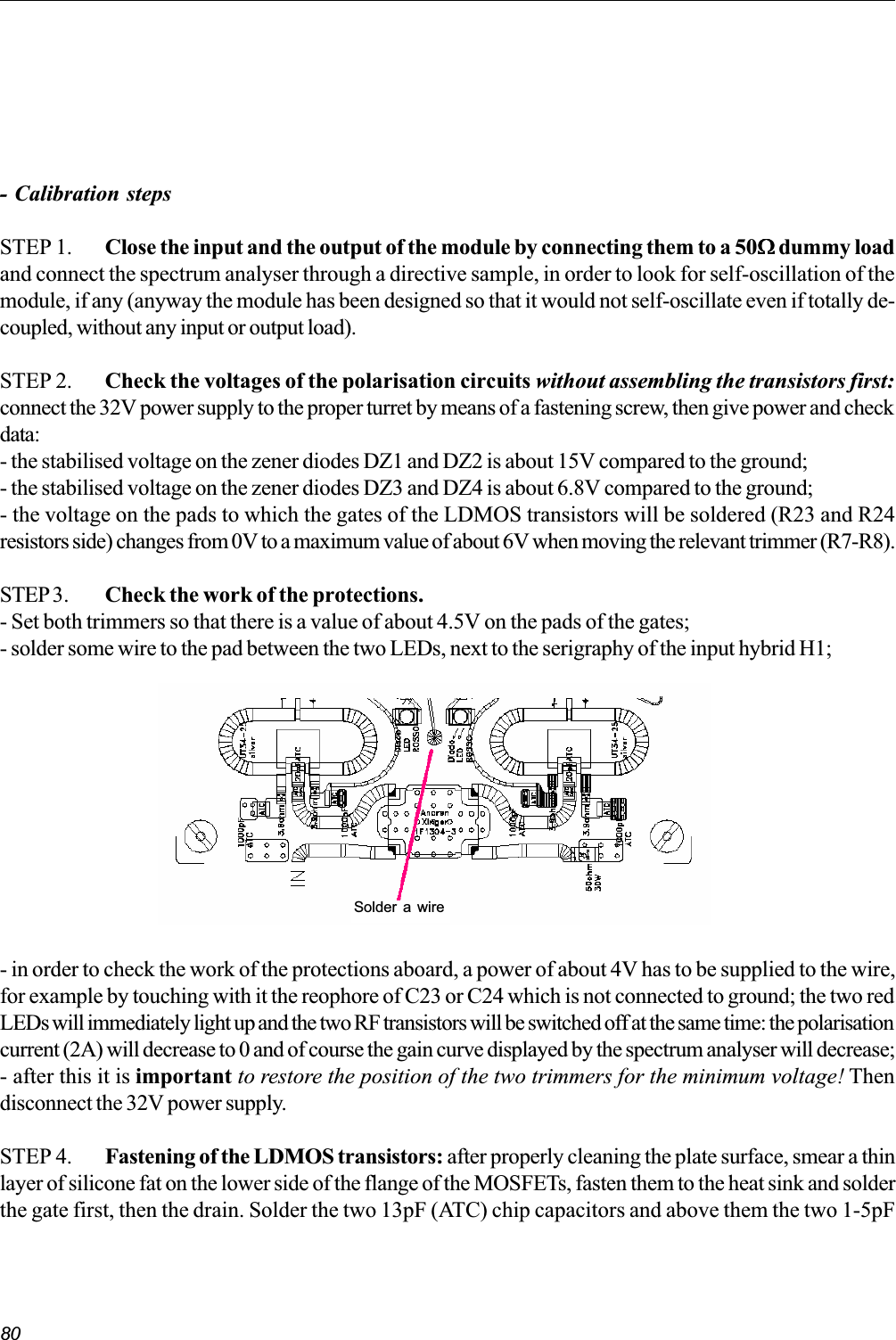
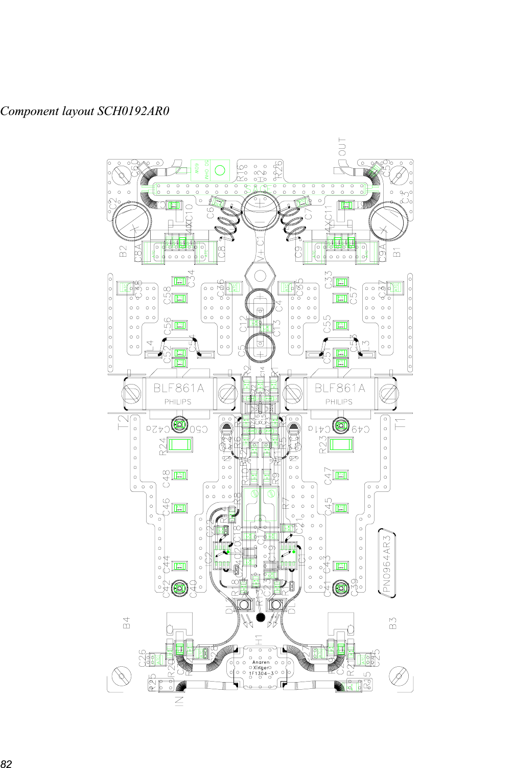
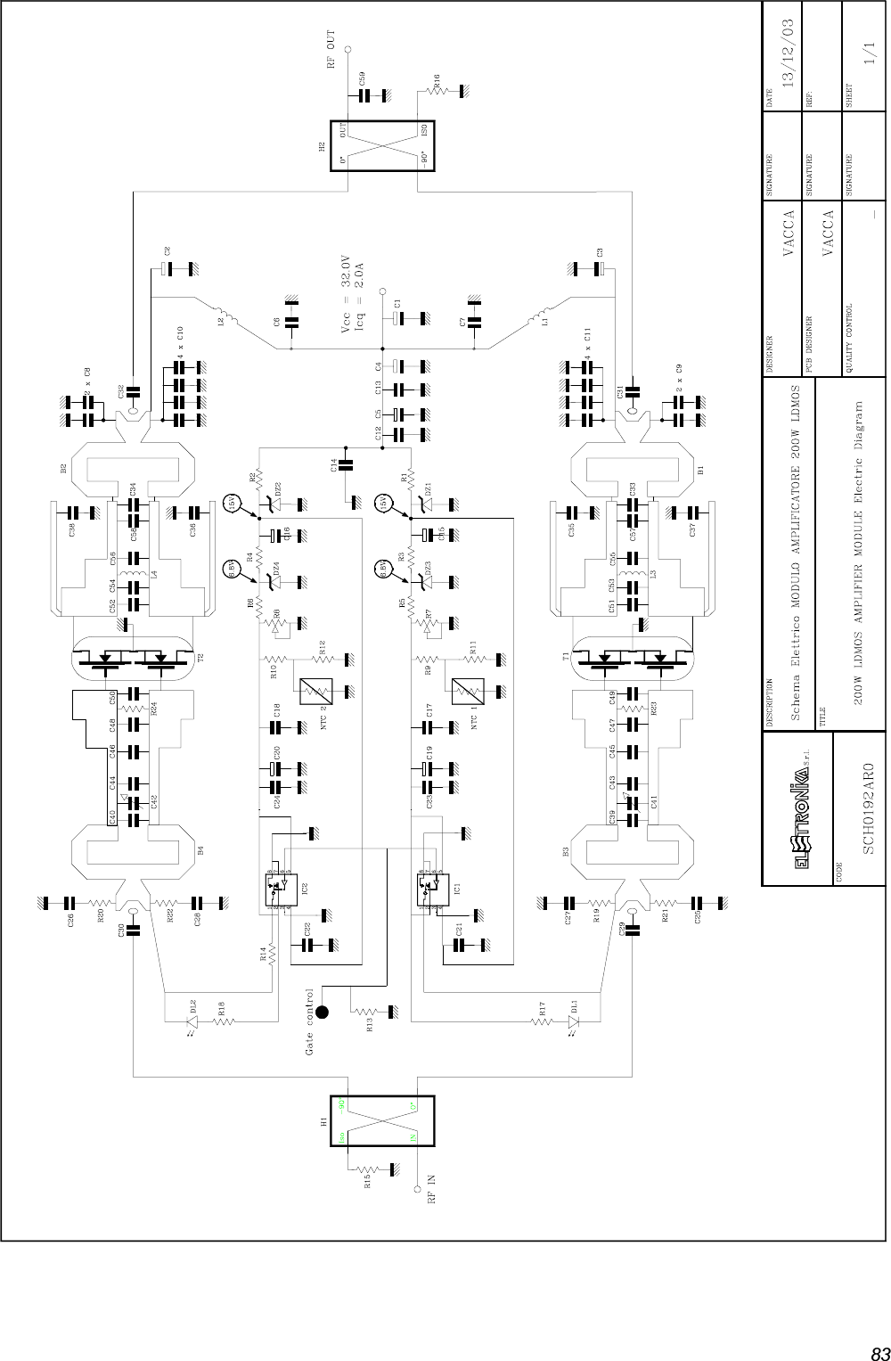
User manual Part 2