Elettronika S r l TXUP2500 2.5 kW Analog TV broadcast transmitter User Manual APT135A AUTV 2500LD Rev0 Date191203 p65
Elettronika S.r.l. 2.5 kW Analog TV broadcast transmitter APT135A AUTV 2500LD Rev0 Date191203 p65
Contents
- 1. User manual Part 1
- 2. User manual Part 2
- 3. User manual Part 3
User manual Part 3
87
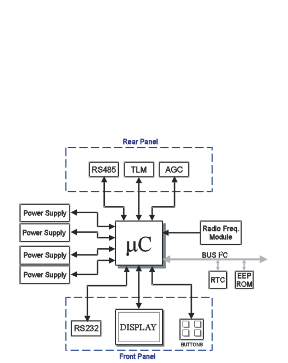
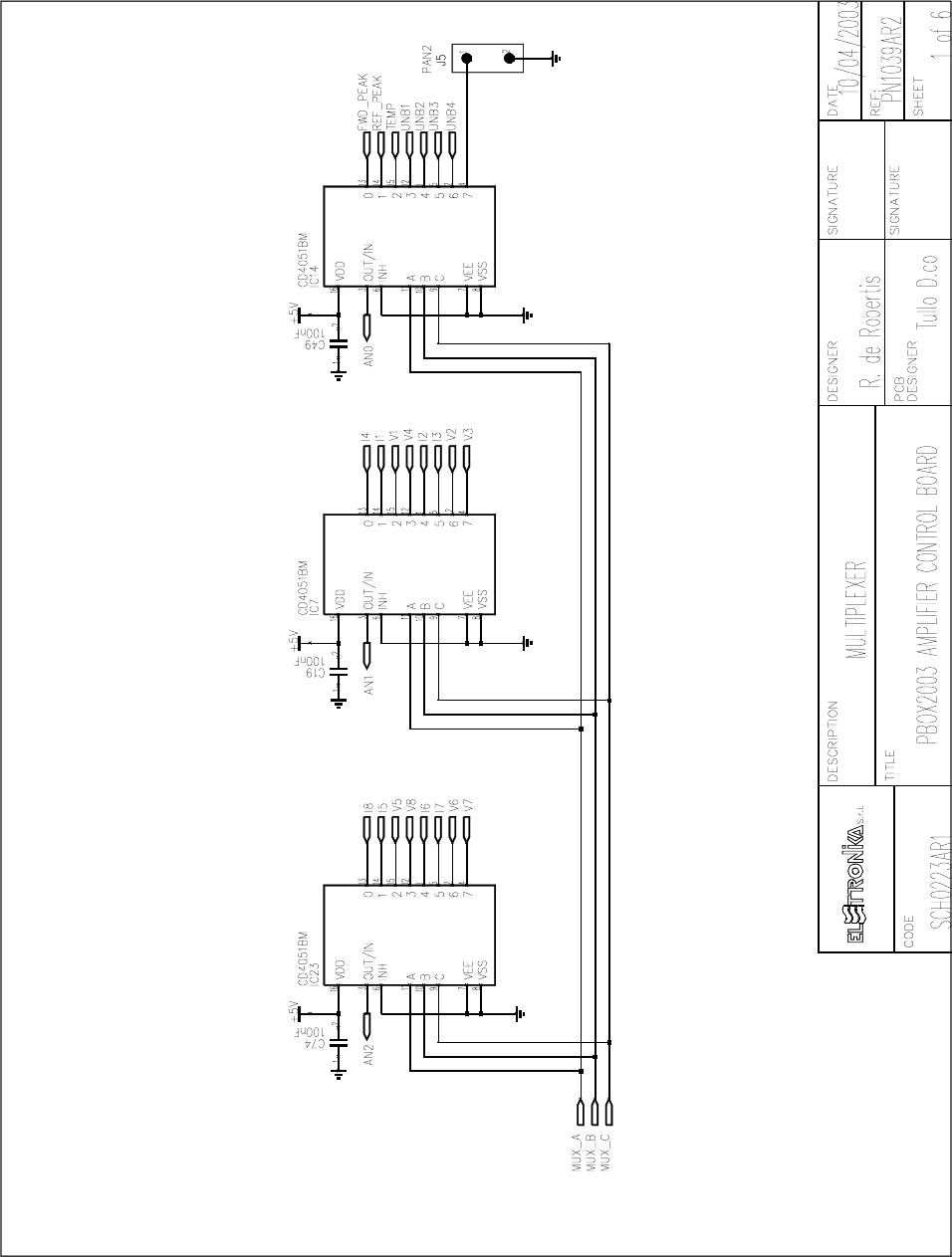
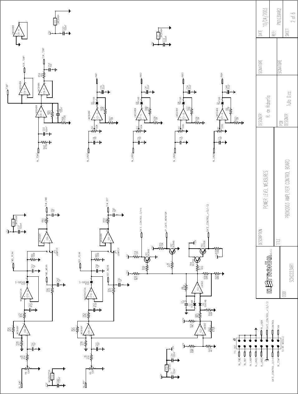
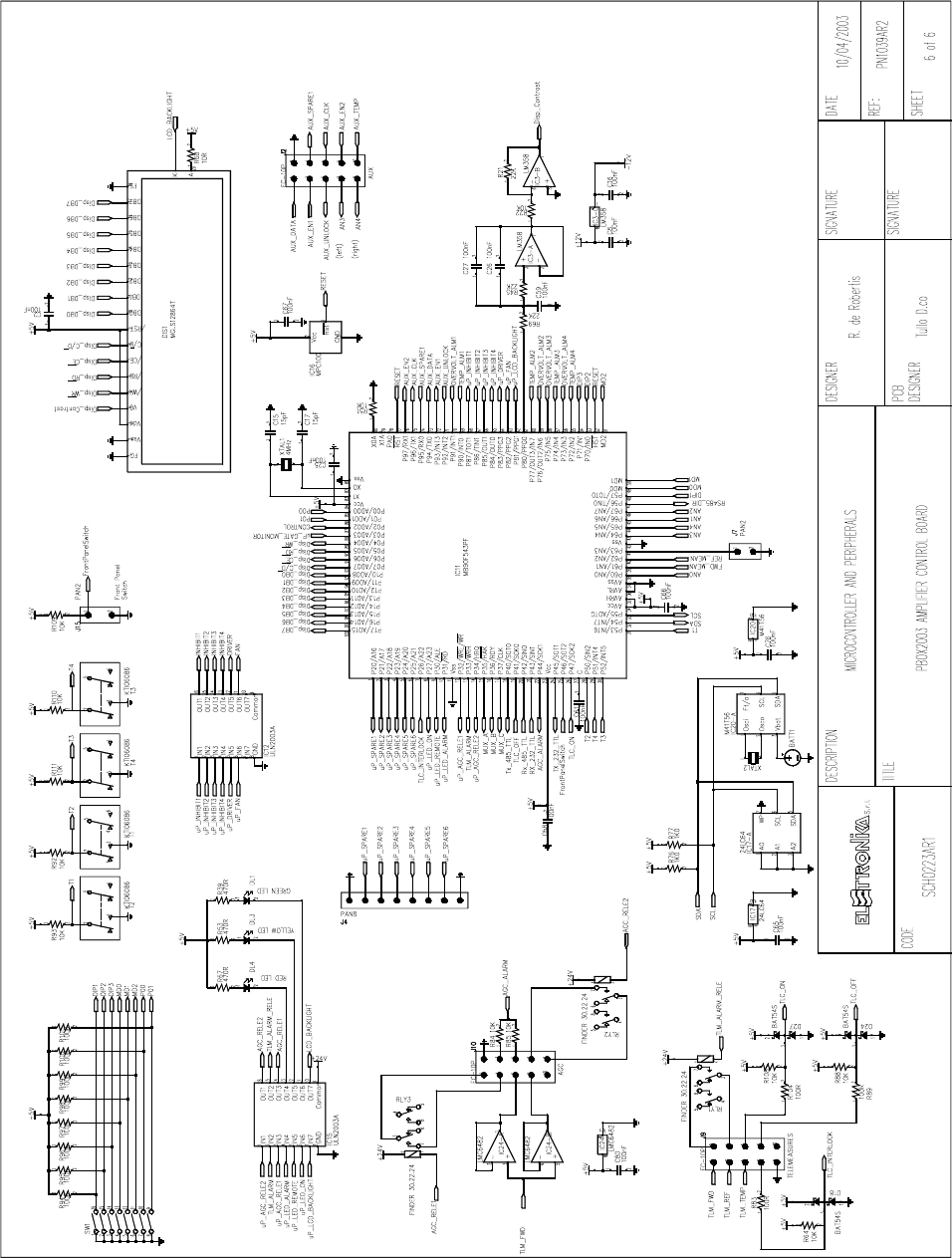
Picture 1: Simplified block diagram of the control and display board
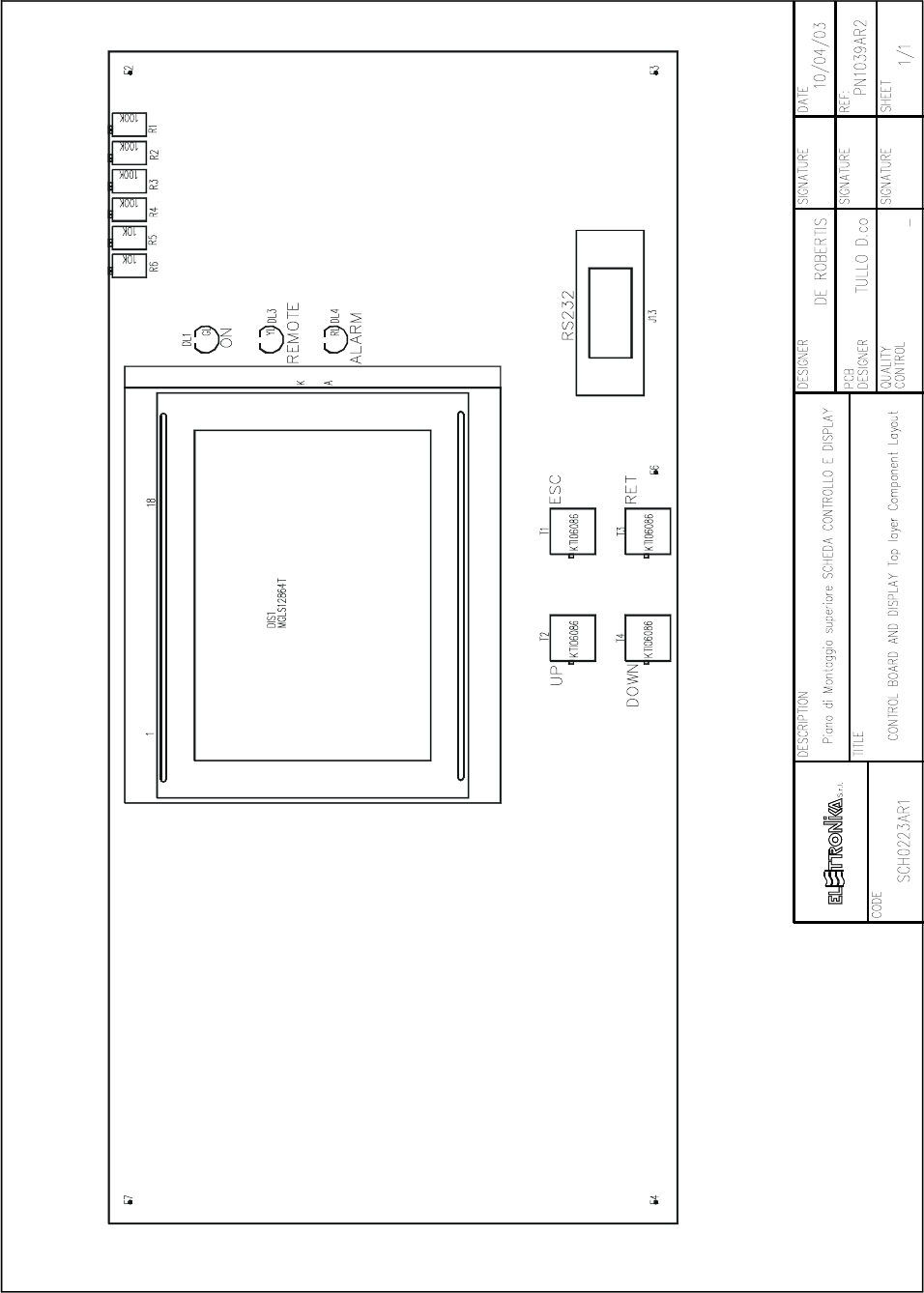
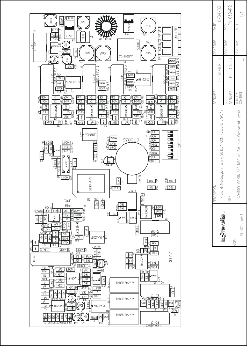
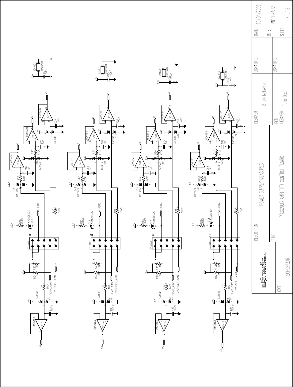
CONTROL BOARD AND DISPLAY SCH0223AR1
DESCRIPTION
The control board SCH0223AR1 manages the operational logic of the amplifier: switching on and off, power
supply and fans, alarms and protections, remote control, human-machine interface. There are managed by a
modern and powerful 16 bit micro-controller (MB90F543), made by Fujitsu, which is the main part of the
board.
Picture 1 shows the block diagram.
88
It can be seen that the micro-controller is the heart of the control system, to which the various peripherals
(power supply, serial ports, telemeasure socket, AGC port, RF amplifier module, ROM, clock, display and
keys) are interfaced.
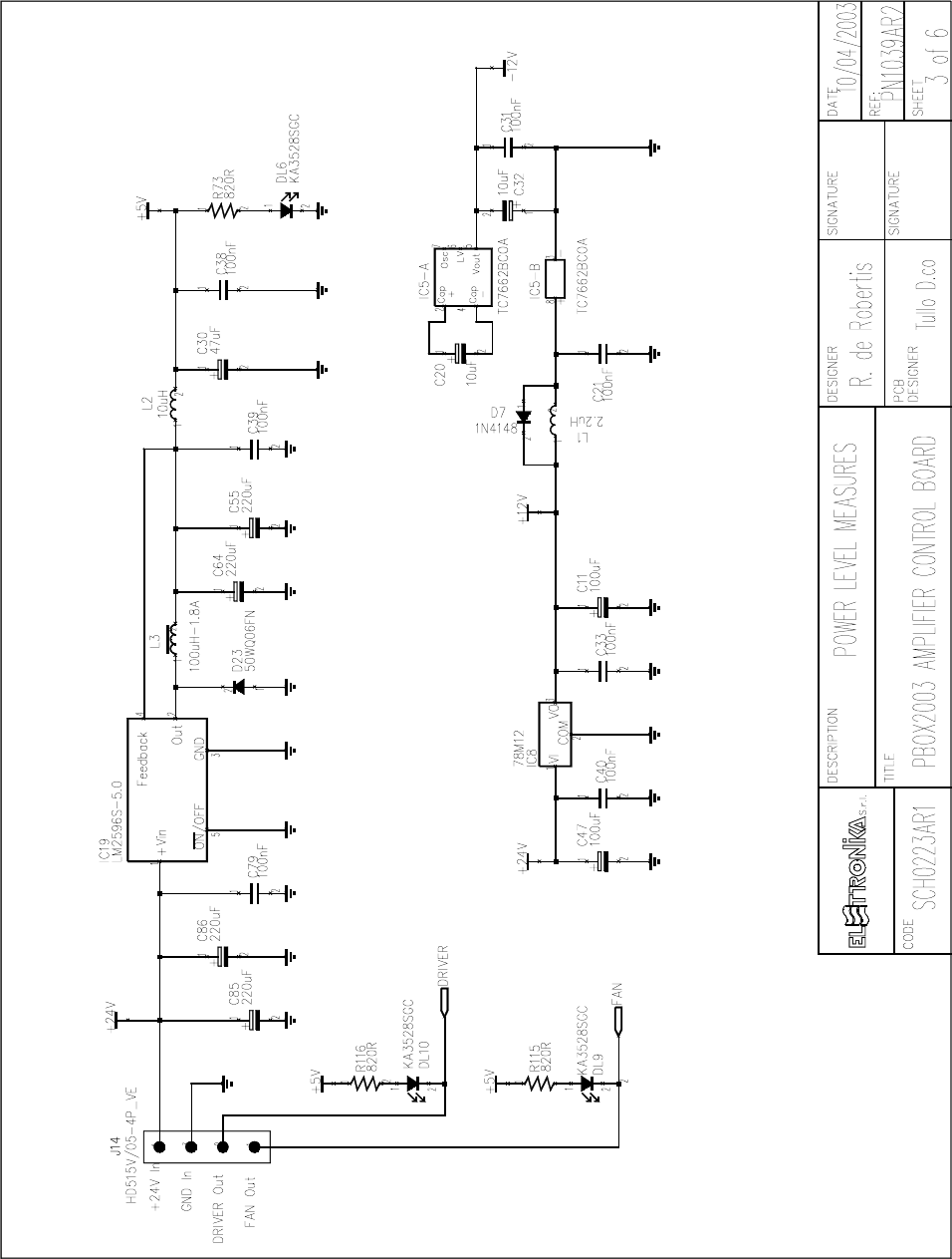
- Power Supply
The board is powered with a continuous +24V voltage from which the +5V voltage powering the most of the
chips (micro-controller, operational amplifiers, display, etc.) is derived by means of a switching converter (see
IC19). A +12Vdc voltage is obtained from it as well, by means of a linear conversion provided by the
integrated circuit IC8. From this, a -12Vdc voltage is obtained by means of the integrated circuit IC5. The
-12V voltage is also used to adjust the contrast of the display.
- Connectors
On the board SCH0223AR1 there are several connectors used as interfaces for the peripherals of the apparatus
and the ports for external communication.
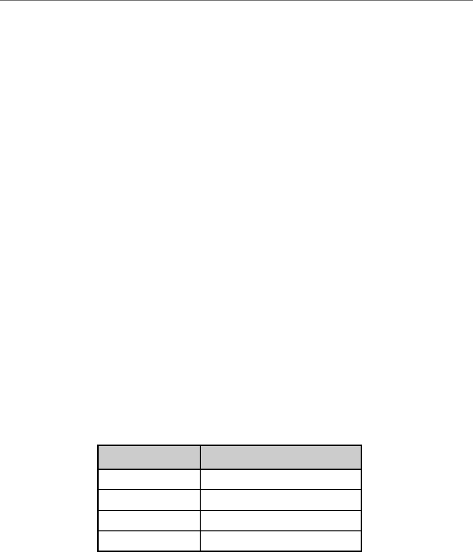
POWER SUPPLY
The connectors J1, J6, J8 e J12 are connected to the power supply powering the RF amplifier modules. The
number of power supply used changes depending on the amplifier, up to four power supply. They are connected
in the order shown in Table 1 below. Remaining connectors, if any, are left unused.
Table 1: Interface connectors for the power supply
Through this connection, each power supply provides the two levels of voltage and current acquired by the
micro-controller by means of an internal ADC. Besides the connectors allow the control board to turn on or
off the individual power supply (for instance when an alarm occurs). The used power supply are protected
CONNECTOR POWER SUPPLY N°
J1 1
J6 2
J8 3
J12 4
89
agaimst voltage surges or temperature increases. If one of these events occurs, the power supply is switched
off and the event is signalled to the micro-controller through the connection with the control board.
RF AMPLIFICATION
The J3 connector interfaces the control board with the RF amplification section. Through this connector the
micro-controller acquires the sample of forward and reflected power, unbalancing (if any), and temperature
of the critic amplification area. It also allows to inhibit the transistors in case of reflected power alarm, by
means of a totally hardware, thus extremely fast protection.
Depending on the apparatus, this connector may also allow to enable or disable the cooling fans of the critic
area.
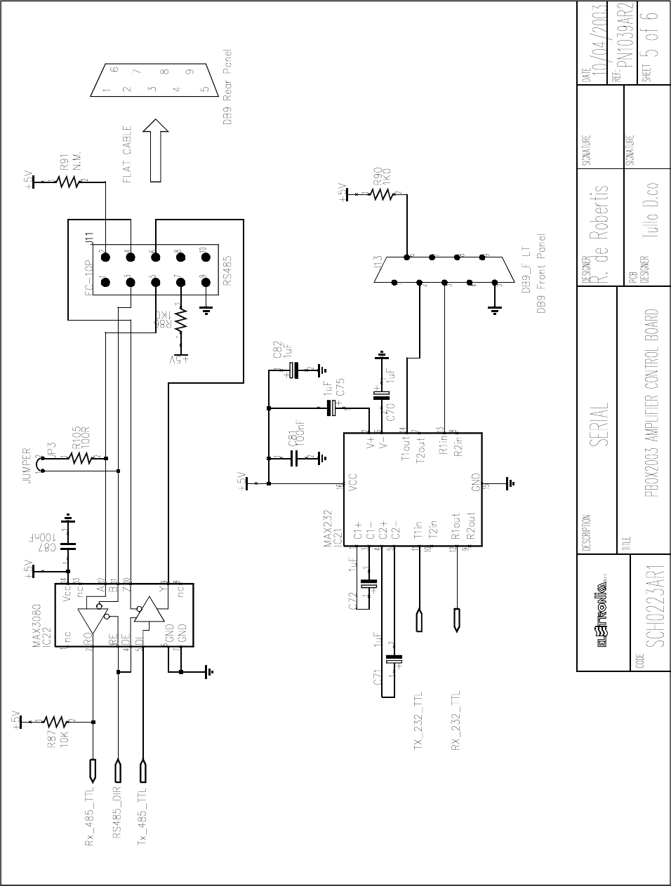
RS485
The J11 connector (10 pin socket) is directly wired to a DB9 female connector placed on the rear panel of the
apparatus. This communication bus allows to connect the amplifier to the control (Amplifier Control) module
of a high-power transmitter composed by several individual amplifiers. In this case, each amplifier and the
Amplifier Control are connected to the same 4-wires RS485 bus and each of them as a unique address
(which can be set by means of the keys and the display) for correct communication.
In case of single (stand-alone) amplifier, the RS485 connector can be used for connection to the Remote
Control Unit (RCU) made by Elettronika S.r.l. This unit allows to monitor and control the remote transmitter
from any site provided with PSTN or GSM1 phone connection.
Table 2 shows the wiring between the J11 connector on the board and the DB9 female connector on the rear
panel, along with the description of the lines.
1 For more details about the control system contact the distributor or the manufacturer.
PIN N°
ON DB9
PIN N°
ON J11 DESCRIPTION
11 Not used
23 Rx-
35 Rx+
47 +5V
59 GND
62 Not used
74 Tx-
86 Tx+
98 Not used
Table 2: Description of the RS485 connector
90
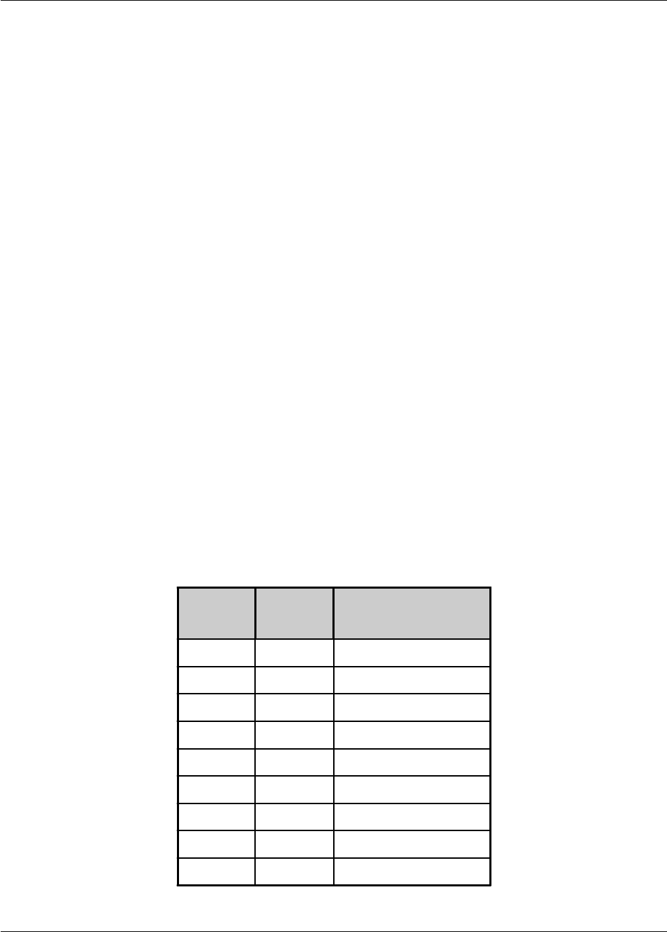
TELEMEASURES
The J9 telemeasure connector (10 pins socket) is directly wired on a DB9 female connector placed on the
rear panel. There are input and output digital lines (TTL level) and analog output lines on this connector, which
are used to monitor and control the amplifier by means of a general-purpose remote control system.
The correspondende between the pins of the J9 connector on the board and the DB9 female connector on the
rear panel, as well as the meaning of the various lines, is shown in table 3 below (the directions refers to the
position of the micro-controller on the board).
PIN N°
ON DB9
PIN N°
ON J9 TYPE DIRECTION DESCRIPTION
1 1 Analog Output Forward power
2 3 Analog Output Reflected power
3 5 Analog Output Temperature
4 7 Digital Input
Interlock:
0V = Interlock Alarm
5V = Normal
59 - -Ground
6-7 2-4 Digital Output Free Contact
(closed when amplifier is in alarm)
8 6 Digital Input Turning-on control
(usually high, active when low)
9 8 Digital Input Turning-off control
(usually high, active when low)
Table 3: Description of the telemeasures connector
The input stage of the digital controls has an internal pull-up towards the 5V power supply voltage. To use this
lines it only takes setting a switch to close to earth, when closed, the relevant control (turning on or off) is
enabled and the switch may be switched open again (impulse controls).
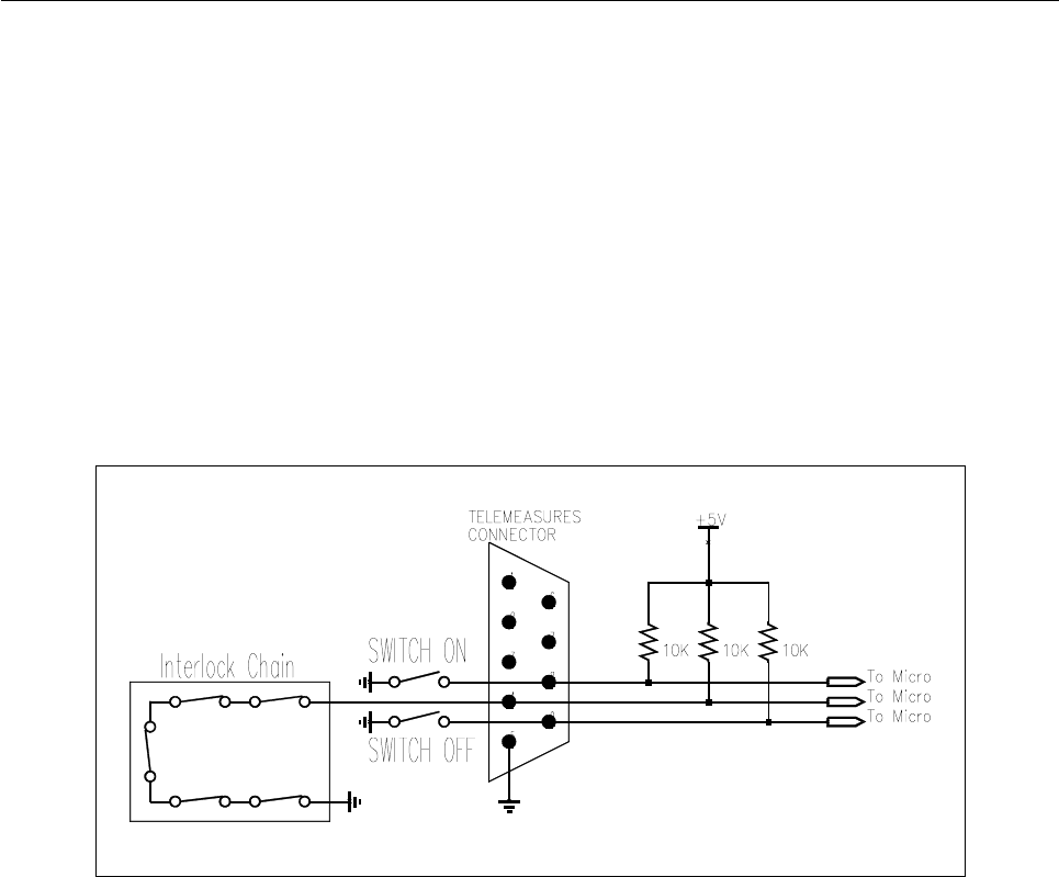
The interlock pin may be used as protection so that the amplifier is switched off the digital input level is low. It
is possible to use several serially connected switches to make an interlock chain. Usually all switches are
closed and the interlock level is low, thus the amplifier is on. If even only one of the switches is opened, the
(*)
(*)
(*) You can select by means of two jumpers on the board (JP1 and JP2) RMS or peak power. If there are two jumpers on pins 1 and 2 of
JP1 and JP2 connector, RMS power is selected. Otherwise, if there are two jumpers on pins 2 and 3 of the same connectors, peak power
is selected.
91
Picture 2: Usage of the digital input signals of the telemeasures connector
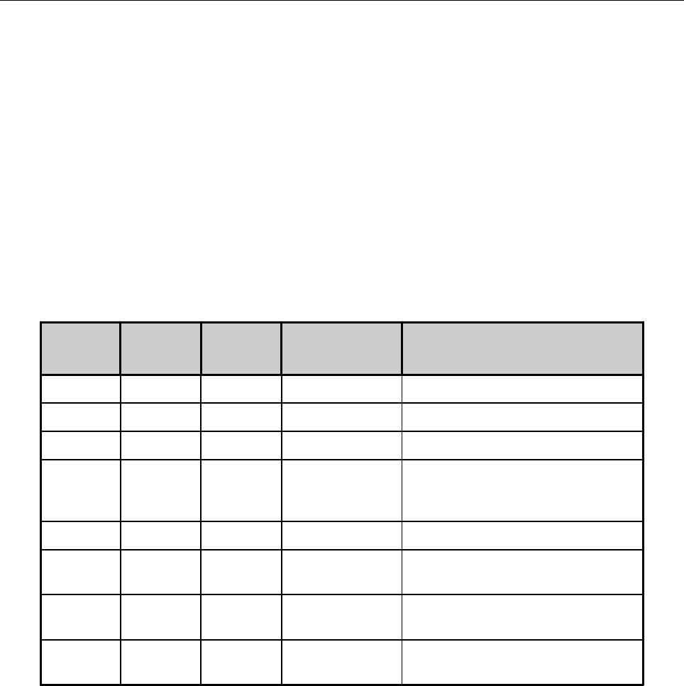
AGC / EXCITER
The connector called J10, as the telemeasures connector and the RS485 bus, is wired to a DB9 female
connector placed on the rear panel of the amplifier. This connectors allow the implementation of an automatic
gain control between an exciter and the amplifier. A voltage signal related to the forward output power
supplied by the amplifier is provided through two pins of the AGC connector. Connecting one of these to the
relevant input pin of the exciter, this can pursuit a given voltage level, so that the output power is always
constant. In order to avoid that, in case of an alarm decreasing the forward power, the exciter strongly
increases the output level due to the AGC, thus damaging the amplification stages, the connector is provided
with two digital output lines called AGC Alarm. Under alarm conditions, this lines are brought by the micro-
controller at a low level, so that the exciter can stop the AGC.
Table 4 shows the connection between the J10 connector on the board and the DB9 connector on the rear
panel, along with the description of each pin (the direction of the pin is referred to the position of the micro-
controller on the board).
level of the interlock signal becomes high (this line has a pull-up towards the +5V power supply voltage as
well) and the protection for interlock alarm is activated for the amplifier, which is switched off. Note that in
case the interlock protection is not used, the pin 4 of the DB9 telemeasure connector and the earth pin (pin 5)
must be short circuited. Otherwise it is possible to disable the monitoring of the interlock chain from menu (see
user manual).
Picure 2 shows a usage for the digital input signals to turn on and off the amplifier and for the interlock alarm.
92
Table 4: Description of the AGC connector
RS232
The DB9 female connector on the front panel is an external communication RS232 serial port, through which
a PC can be connected directly to the amplifier in order to perform operations such as the remote control (by
means of an adequate software2) and the update of the microcontroller firmware.
The used communication protocol is asynchronous, at a 19200bps speed, 1 start bit, 8 data bits, 1 stop bit,
no parity. No hardware flow is used. The connector is DCE type and the pin used are shown in Table 5.
PIN N° ON DB9 123456789
DESCRIPTION -TxDRxD-GND----
MISCELLANEOUS
The J2 (called AUX), J4, J5 and J17 connectors are not used and are there only for future updates. The SW1
dip-switches are partially used for the configuration of the correct mode for the micro-controller. The other
switches are not used. It is important that the position of the dip-switches is left unchanged, because changing
it may set a wrong mode for the micro-controller, affecting the work of the whole amplifier.
2 For more information about this application contact the distributor of the manufacturer.
PIN N°
ON DB9
PIN N°
ON J10 TYPE DIRECTION DESCRIPTION
11- -Ground
23DigitalOutput
AGC Alarm
0V = Alarm
5V = Normal
35DigitalOutput
AGC Alarm
0V = Alarm
5V = Normal
47- -Not used
59 - -Not used
62 - -Not used
7 4 - - Nout used
8 6 Analog Output Forward power
9 8 Analog Output Forward power
Table 5: Description of the RS232 connector
93
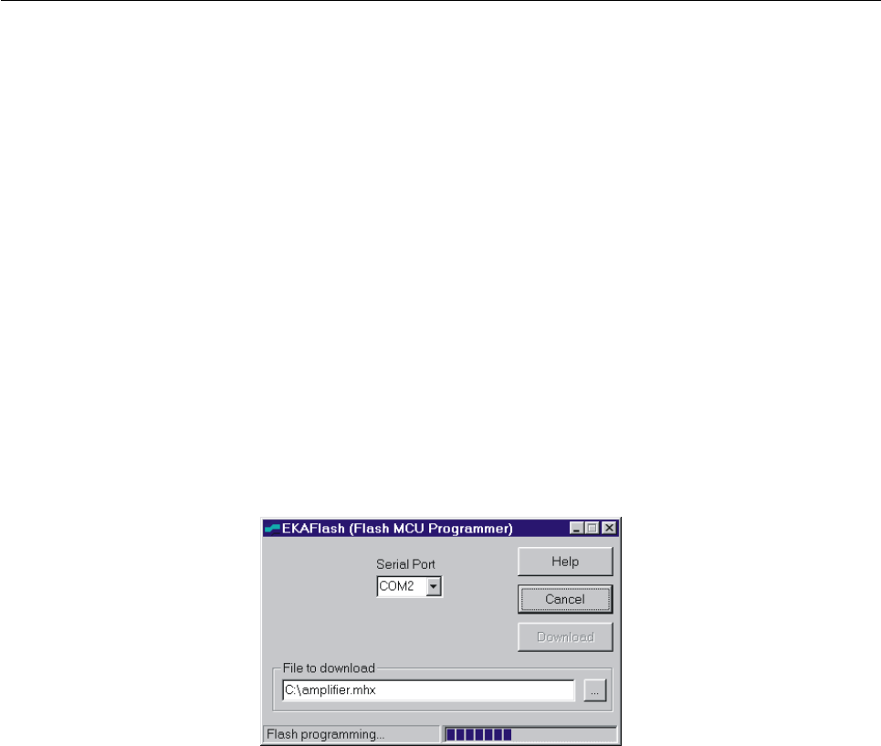
FIRMWARE UPDATE
The micro-controller MB90F543 is provided with a built-in Flash memory containing the firmware. The
firmware can be updated to later versions without removing the apparatus from the rack and/or replacing the
chip.
To upgrade it, connect a PC to the RS232 socket on the front panel of the apparatus by means of a cable
DB9 male - DB9 female (pin-to-pin).
Launch on the PC the EKAFlash application, select the serial port in use of the PC and choose the update file
by pressing the ... key and click on Download button.
Eventually, turn off the amplifier from the main switch and then turn it on again. The upgrade of the firmware
begins on the EKAFlash window. Picture 3 shows this window while a firmware is being updated.
Picture 3: The EKAFlash window while updating a firmware
94
95
96
97
98
99
100
101

102
COMPONENT LIST SCH0223AR1
Part Name/Number Description Qty. Comps. Page 1/2
BATT BH001RB 3093_90 03093 03090 BATTERY HOLDER 1 BATT1
CC 100nF-S 01065C 01065C Y5V 1206 COND 46 C2, C7-10, C12, C16, C19, C21-27
C29, C31, C33, C37-40, C44-46,
C49, C58-61, C63, C65-69, C74,
C76, C78-81, C83-84, C87, C90
CC 15pF-S 01088 01088 SMD 1206 COND 4 C13-15, C17
CC 1nF-S 01096 01096 SMD 1206 COND 7 C3-6, C50-51, C53
CC 1uF100V-S 01760A 01760A Y5V 1206 COND 13 C1, C18, C28, C36, C43, C54,
C56-57, C62, C73, C77, C88-89
CC 47pF-S 01100 01100 SMD 1206 COND 2 C42, C52
CE 100uF25V-S 01793B 01793B ELETTR SMD COND 2 C11, C47
CE 10uF35V-S 01778A 01778A ELETTR SMD COND 2 C20, C32
CE 1uF35V-S 01613A 01613A TANTALIUM ELETTR SMD CO 5 C70-72, C75, C82
CE 220uF50V LOW ESR 1799A ELETTR SMD COND LOW ESR 4 C55, C64, C85-86
CE 22uF16V-S 01780A ELETTR SMD COND 4 C34-35, C41, C48
CE 47uF35V-S 01790A 01790A ELETTR SMD COND 1 C30
D 1N4148-S 03002 03002 SMD DIODE 7 D1-2, D5-9
D 50WQ06FN 03019A SMD DIODE SCHOTTKY 5,5A 1 D23
D BAS85-S 03024 SMD DIODE SCHOTTKY 2 D14-15
D BAT54S 03199 SMD SCHOTTKY DIODE A-K T 19 D3-4, D10-13, D16-22, D24-29
DIS MGLS12864T 03083A 128x64 DOT (BLUE-LED WH 1 DIS1
DL KA-3528SGC 03057 03057 GREEN SMD LED DIODE 7 DL2, DL5-10
DL LEDG5 03060 03060 GREEN LED DIODE 5mm 1 DL1
DL LEDR5 03061 03061 RED LED DIODE 5mm 1 DL4
DL LEDY5 03054B 03054B YELLOW LED DIODE 5mm 1 DL3
IC 24LC64 04815 04815 SMD INTEG CIRCUIT 1 IC17
IC 78M12 4307B 04307B SMD VOLTAGE REGULATOR 1 IC8
IC CD4051BM-S 04615 SMD INTEG CIRCUIT 3 IC7, IC14, IC23
IC LM2596S-5.0 04580 SMD INTEG CIRCUIT 1 IC19
IC LM358M-S 04660 04660 SMD INTEG CIRCUIT 1 IC3
IC LM393-S 04639 04639 SMD INTEG CIRCUIT 1 IC2
IC LMC6482-S 04632 SMD INTEG CIRCUIT 1 IC24
IC LMC6484-S 04634 SMD INTEG CIRCUIT 7 IC1, IC4, IC6, IC9, IC13, IC18,
IC25
IC M41T56 04611 04611 SMD INTEG CIRCUIT 1 IC20
IC MAX232-S 04804B 04804B SMD INTEG CIRCUIT 1 IC21
IC MAX3080-S 04770 04770 SMD INTEG CIRCUIT 1 IC22
IC MAX942CSA-S 04572 SMD INTEG CIRCUIT 1 IC10
IC MB90F543PF 04596 SMD INTEG CIRCUIT 1 IC11
IC MPC100-450DI-TO 04608 INTEG CIRCUIT 1 IC16
IC TC7662BCOA 04758A 04758A SMD INTEG CIRCUIT 1 IC5
IC ULN2003A 4870 04870 SMD INTEG CIRCUIT 2 IC12, IC15
IND 2u2H-S 05020A 05020A INDUCTOR 1 L1

103
Part Name/Number Description Qty. Comps. Page 2/2
IND MS85 10uH-S 04948 INDUCTOR 2,7 A 1 L2
IND T100uH-1.8A 4958 04958 TOROIDAL-STORAGE CHOKES 1 L3
J CON HD515V/05-4PVE 02881 + 02882 PANDUIT PCB CONN 1 J14
J DB9_F-0° LT 02794 PCB CONNECTOR DB9 LONG T 1 J13
J FC-10P 02697-02699 02697+02699 PCB CONNECTOR POL 8 J1-2, J6, J8-12
J FC-16P 02701-02700 02701+02700 PCB CONNECTOR POL 1 J3
J PAN2 02739-40-41 02739+02740+02741 PCB CONNECTO 3 J5, J7, J15
J PAN8 02716 02716 PCB CONNECTOR 1 J4
JU JUMP2 02739-02742 02739+02742 MASCHIO PAN2 1 JP3
JU JUMP3 02707-02742 02707+02742 MASCHIO PAN3 2 JP1-2
R 100K-1%-S 00065B 00065B RES 1/4W 1% SMD 1206 10 R65-66, R94-101
R 100R-1%-S 00029D 00029D RES 1/4W 1% SMD 1206 12 R24, R47, R58, R71, R75,R81,
R83, R89, R103-105, R113
R 10K-1%-S 00053B 00053B RES 1/4W 1% SMD 1206 32 R7, R10, R12, R14-16, R22, R25,
R27, R30, R33-34, R36, R38, R51,
R62-64, R78-79, R84-85, R87-88,
R92-93, R106-111
R 10R-S 00017A 00017A RES 1/4W 5% SMD 1206 1 R68
R 1206 NOT MOUNTED NOT MOUNTED RES 1/4W 5% SMD 12 1 R91
R 1K0-1%-S 00041B 00041B RES 1/4W 1% SMD 1206 8 R17, R54, R59-60, R76-77, R86,
R90
R 22K-1%-S 00057B 00057B RES 1/4W 1% SMD 1206 11 R9, R21, R26, R28-29, R37, R45,
R48-50, R69
R 2K2-1%-S 00045B 00045B RES 1/4W 1% SMD 1206 3 R52, R55, R61
R 470K-S 00073A 00073A RES 1/4W 5% SMD 1206 11 R8, R23, R40, R42, R46, R57, R70
R74, R80, R102, R112
R 470R-1%-S 00037B 00037B RES 1/4W 1% SMD 1206 6 R11, R13, R39, R53, R56, R67
R 4K7-1%-S 00049B 00049B RES 1/4W 1% SMD 1206 3 R18, R31, R43
R 68K-1%-S 00063B 00063B RES 1/4W 1% SMD 1206 4 R19-20, R32, R44
R 820R-S 00040A 00040A RES 1/4W 5% SMD 1206 7 R35, R72-73, R82, R114-116
R 8K2-1%-S 00052B 00052B RES 1/4W 1% SMD 1206 1 R41
RL 30.22.24 07569 07569 RELE 3 RLY1-3
RV 100K-3266X 00814 VARIABLE RESISTOR 4 R1-4
RV 10K-3266X 00807 00807 VARIABLE RESISTOR 2 R5-6
SW SWITCH-8DIP 07530A PCB DIP SWITCH SMD 1 SW1
T 06086 N 7630 7632 7630 7632 KTI06086 PULSANTE 2 4 T1-4
TR BC848 03457 03457 NPN SMD TRANSISTOR 2 TR1-2
TR BC856 03455 03455 PNP SMD TRANSISTOR 2 TR3-4
XTAL 32.768k-S 05146 05146 QUARTZ 1 XTAL2
XTAL 4MHz-S 05101A 05101A QUARTZ 1 XTAL1
104
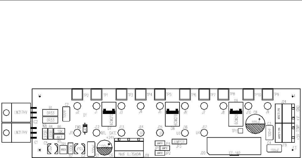
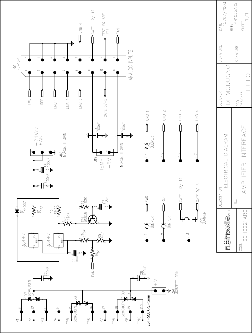
AMPLIFIER INTERFACE SCH0221AR0
Component layout SCH0221AR0
COMPONENT LIST SCH0221AR0
Part Name/Number Description Qty. Comps.
CC 100nFAVX 01065A 01065A CERAMIC COND 4 C1-4
CE 100uF100V 01795B ELETT. COND. 1 C8
CE 100uF50V 01795 01795 ELETT. COND. 1 C6
CE 10uF35V-S 01778A 01778A ELETTR SMD COND 2 C5, C7
D 1N4007 03009 03009 DIODE 1 D1
D 6CWQ10FN 03026 SMD DIODE SCHOTTKY 3,5A 3 D7-9
IC LM317HV 04340A INTEG CIRCUIT 2 IC1-2
J FC-16P 02701-02700 02701+02700 PCB CONNECTOR POL 1 J20
J SCREWCONN2 02853 02853 PCB SCREW CONNECTOR 2 J19, J24
J SCREWCONN3 02860 02860 PCB SCREW CONNECTOR 1 J18
J TESTP1.3mm 07913 07913 TEST POINT 17 J1-17
JU JUMP2 02739-02742 02739+02742 MASCHIO PAN2 3 JP1-2, JP4
JU JUMP3 02707-02742 02707+02742 MASCHIO PAN3 1 JP3
R 0R33-1W-S 00380 RES 1W 5% SMD 2512 2 R1-2
R 100K-S 00065A 00065A RES 1/4W 5% SMD 1206 1 R7
R 10K-S 00053A 00053A RES 1/4W 5% SMD 1206 1 R6
R 220R-S 00033A 00033A RES 1/4W 5% SMD 1206 1 R4
R 270R-S 00034A 00034A RES 1/4W5% SMD 1206 1 R3
R 4K7-S 00049A 00049A RES 1/4W 5% SMD 1206 1 R5
TR BC856 03455 03455 PNP SMD TRANSISTOR 1 TR1
105
106
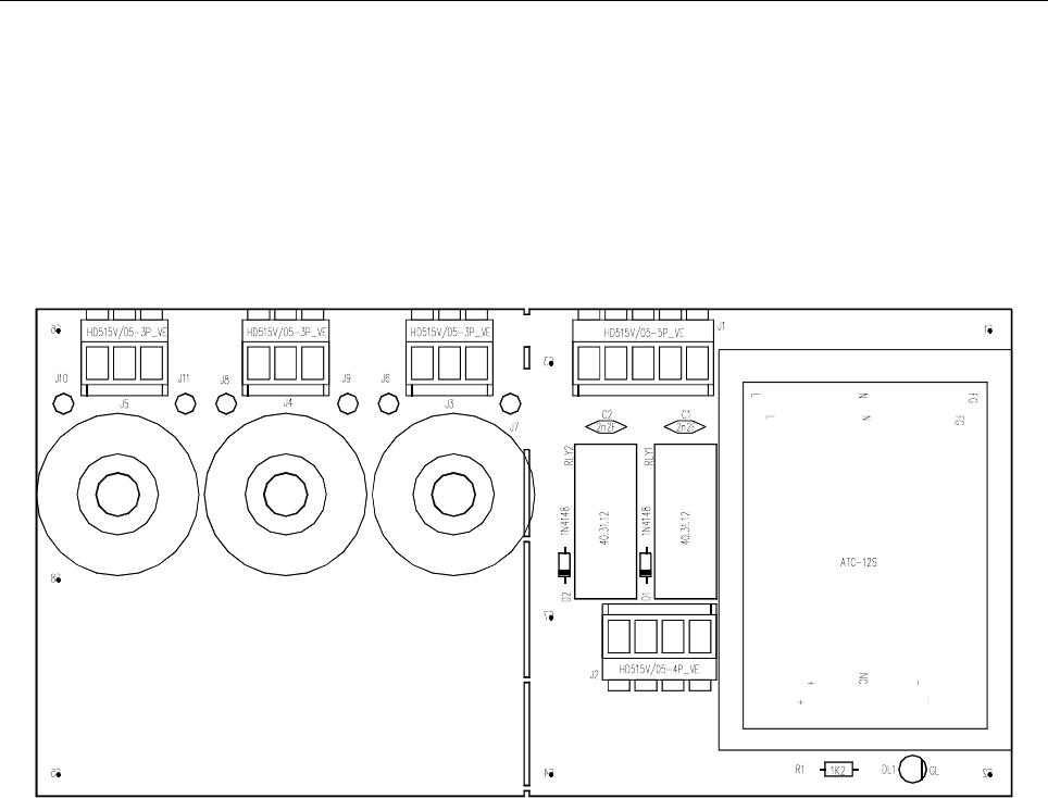
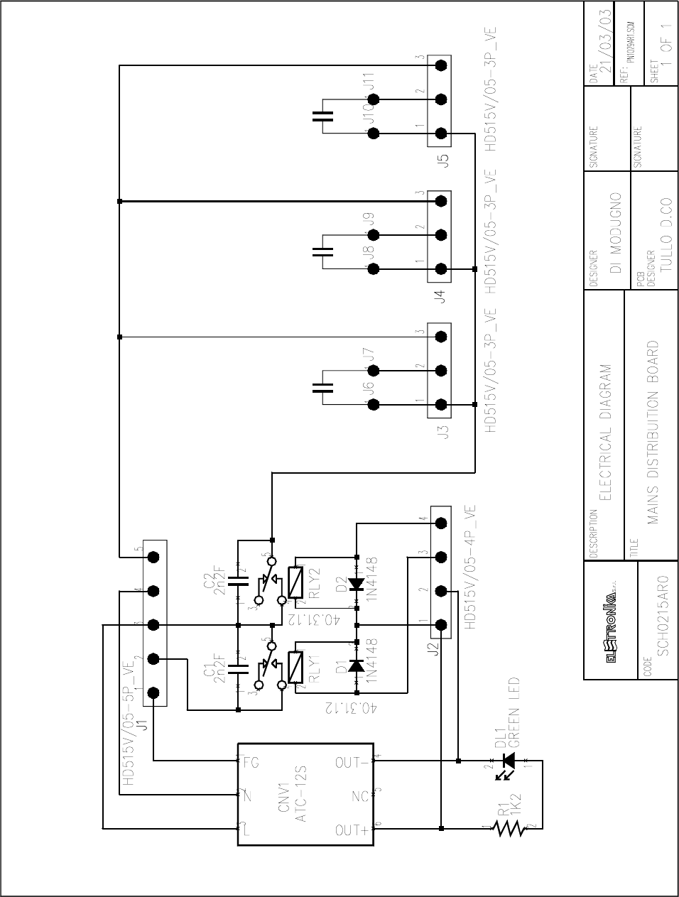
MAINS DISTRIBUTION BOARD SCH0215AR0
Component layout SCH0215AR0
COMPONENT LIST SCH0215AR0
Part Name/Number Description Qty. Comps.
CC 2nF2 2kV 01045A 01045A CERAMIC COND 2 C1-2
CNV AC-DC ATC-12S AC DC CONVERTER 1 CNV1
D 1N4148 03001 03001 DIODE 2 D1-2
DL LEDG3 03053 03053 GREEN LED DIODE 3mm 1 DL1
J CON HD515V/05-3PVE PANDUIT PCB CO 3 J3-5
J CON HD515V/05-4PVE 02881 + 02882 PANDUIT PCB CONN 1 J2
J CON HD515V/05-5PVE PANDUIT PCB CO 1 J1
J TESTP1.3mm 07913 07913 TEST POINT 6 J6-11
R 1K2 0042 0042RES 1/4W 5% 1 R1
RL 40.31.12 07567 07567 RELE 2 RLY1-2
107
108
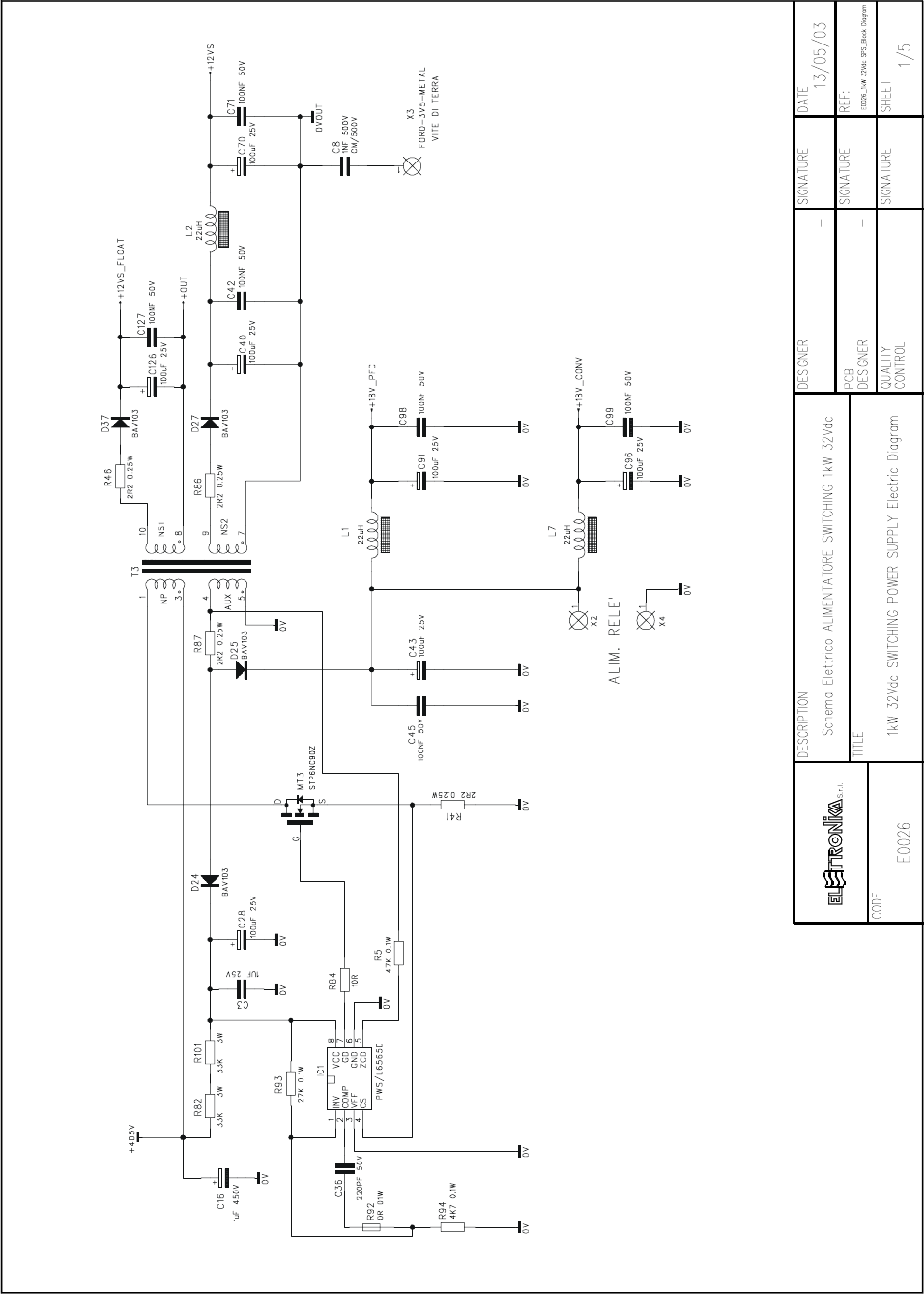
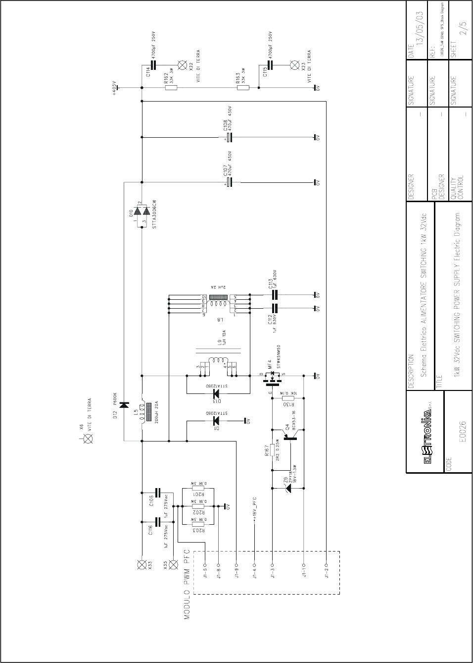
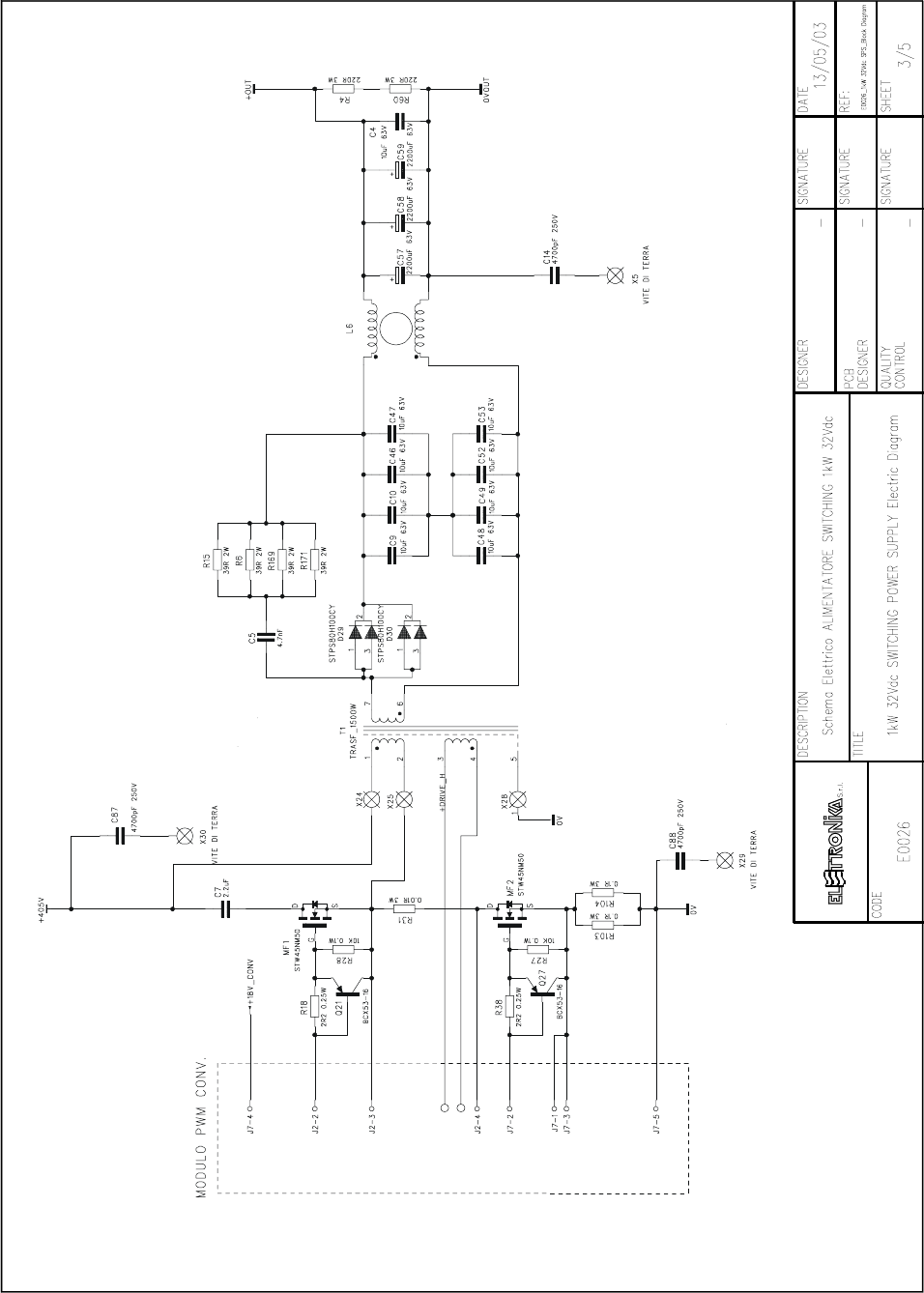
TECHNICAL CHARACTERISTICS
- Input characteristics
Vin: 100..240Vrms
REND.: 80%
lin@FL: 16..6,5Arms
PF>0.95@FL (PFC)
- Output characteristics
Pout: 1300W on 2 outputs
Vout: 2 options a) 32Vdc 40A on 2 outputs
b) 52Vdc 25A on 2 outputs
Block Diagram
1kW 32Vdc SWITCHING POWER SUPPLY E0026
AUX
PRIM
AUX
AUX
SEC
L R
N S
T EMI
FILTER
PFC
POWER
STAGE
MAIN
CONVERTER
POWER
STAGE
+1
1
+2
+2
OUTPUT
CONTROL
AND
PROTECTION
MONITOR
FLAT
10PIN
Feedback
inhibit
inhibit
109
110
111
112
113
114
115
116

117
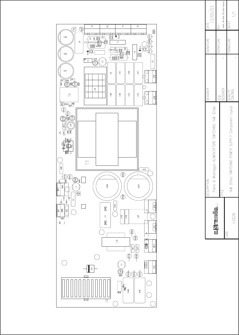
COMPONENT LIST 1kW 32Vdc Switching Power Supply
SMT COMPONENT
IT QTY STORE-CODE DESCRIPTION REF. Page 1/2
1 1 03.B04.0000A CHIP RES.0805 STR.MET.0.10W 0Ohm 5% R92
2 2 03.B05.0003B 100R 1% 0.1W RES. SMD 0805 100PPM R16, R42
3 3 03.B05.0006B 10K 1% 0.1W RES. SMD 0805 100PPM R27-28, R130
4 4 03.B05.0009B 1K 1% 0.1W RES. SMD 0805 100PPM R8, R40, R43, R105
5 3 03.B05.0014B 27K 1% 0.1W RES. SMD 0805 100PPM R20, R45, R93
6 1 03.B05.0020B 47K 1% 0.1W RES. SMD 0805 100PPM R5
7 3 03.B05.0061B 4K7 1% 0.1W RES. SMD 0805 100PPM R19, R44, R94
8 1 03.B05.0150B 150R 1% 0.1W RES. SMD 0805 100PPM R84
9 6 03.B10.0267B 4K75 1% 1% 25W RES. SMD 1206 100PPM R47-52
10 9 03.B17.0003B 2R2 1% 0.25W RES. SMD MINIMELF 100PPM R1-2, R18, R38, R41, R46,
R86-87, R167
11 2 03.B17.0010B 100K 1% 0.25W RES. SMD MINIMELF 100PPM R75-76
12 1 03.B25.0002A 0.01R 1% 3W RES. SMD 4527 WSR3 100PPM R31
13 8 03.D02.0004A COND. CRM MSTR Z5U 100NF 50V 20% SMT-0805 C13, C42, C45, C50, C71,
C98-99, C127
14 3 03.D02.0012A 220PF 50V 5% 0805 SMD COND. CMR X7R C11, C19, C36
15 3 03.D04.0004A 1NF 500V 10% 1206 SMD COND. CRM MSTR C8, C93-94
16 5 03.D04.0007A 1uF 25V 10% 1206 SMD GRM42-6 (MURATA) C1, C3, C12, C18, C135
17 1 05.B02.0014A L6565D FLYBACK QUASI-RESONANT CONTROL. IC1
18 2 05.B04.0010A LMC6482AIM DUAL CMOS SOP-8 OP.AMP UI-2
19 2 04.D00.0001A MMBT2222A BJT NPN 40V 1A 0.35W Hfe100-300 Q3, Q20
20 1 04.D00.0501A MMBT2907A BJT PNP -60V 0.8A 0.35W Hfe100-300 Q1
21 5 04.D00.0502A BJT PNP -80V -1A 1W Hfe 100 Ty. BCX53-16 Pk. SOT-89
(M.code: AL) Q4, Q18, Q21-22, Q27
22 6 04.B01.0001A BAV103 SMD DIODO SILICIO 200MA 250V PKG. SOD80 D1, D22, D24-25, D27,
D37
23 3 04.K00.0002A DIODO LED VERDE SMD 1206 BRIGHTLED DL1-3
THT COMPONENT
IT QTY STORE-CODE DESCRIPTIO REF. Page 1/2
24 1 CIRCUITO STAMPATO D.N. D06.0203A_00R02
25 4 Morsetto Phoenix MKDS5/2-9.5 J4, J6, J9-10
26 1 RELAY 24VDC 16A G2R-1-E-24VDC OMRON K1
27 5 0,1R 5% 3W RES. OSSIDO. MET. R103-104, R201-203
28 2 220R 5% 3W RES. OSSIDO. MET. R4, R60
29 2 33KOhm 5% 3W RES. OSSIDO MET. R162-163
30 4 39R 5% 2W RES. OSSIDO MET. 250ppm R6, R15, R169, R171
31 2 100K 5% 2W RES. OSSIDO MET. 250ppm R82, R101

118
IT QTY STORE-CODE DESCRIPTION REF. Page 2/2
32 4 RESISTORE A FILO 0,01R 2W 5% R3, R7, R29, R34
33 1 Potenziometro Cermet 20Giri 2KOhm 0.5W 10% 100ppm
Ty: 67W P1
34 5 4700pF 250W COND. CRM CLASSE X1 Y2 P.7,5 C6, C15, C17, C87-88
35 1 100nF 600V 5% Cond. film mylar scat 7.5x17.5mm P.15 C2
36 2 1UF 275Vac X2COND. FILM. SCAT. 12.5x32.5mm P27.5 C106, C116
37 1 COND. FILM MYLAR SCATOLINO 4.7nF 250V 10% 5x17.5
P. 15 (mm) C5
38 2 1uF 630V COND. FILM SCAT. 18x32.5mm P.27.5 C112-113
39 9 10uF 63 COND. RAD. POLIES. 10% P22.5 10x25 (mm) C4, C9-10, C46-49, C52,
C53
40 1 Condensatore FILM SCATOLINO 2.2uF 400V 10% P.27,5 C7
41 2 470uF 450V 20% ETL SNAP-IN 20% ins. Radiale d35 / h52mm C107-108
42 7 COND. ETL AL 100uF 25V d6,3x11mm P.2,5 C28, C40, C43, C70, C91,
C96, C126
43 3 COND. ETL AL 220uF 63V 20% ins. Radiale d20 / h42mm P7.5 C57-59
44 1 COND. ETL 1uF 450V 20% ins. Radiale d8 / h11.5 P.3.8 (mm) C16
45 3 INDUTTORE 22uH I-MAX 2A PASSO 200 L1-2, L7
46 1 TRASF. DI POT. T0203.04R01 D.N. STT0203_04R01 T1
47 1 TRASF. AUX T0203.05R02 D.N. STT0203_05R02 T3
48 1 BOBINA SNUBBER PFC T0211.03R01 D.N. STT0211_03R01 L9
49 1 BOBINA CLAMPER PFC T0211.02R02 D.N. STT0211_02R02 L8
50 1 BOBINA PFC T0203.01R00 D.N. STT0203_01R00 L5
51 1 BOBINA DI MODO COMUNE T0203.06R00 D.N. STT0203 L6
52 1 NTC 10R DIAM. 9,5mm P.5 B57-235-S100M NTC5
53 1 NTC EPCOS B57045K0103K000 NTC1
54 2 FUSIBILE AUTO AL 25A 32V F3-4
55 4 CLIP PORTAFUSIBILE PER AUTO PZ1011 (OMEGA) F1-2
56 1 P600K DIODO RADDRIZZ. SILICIO 6A 800V D12
57 1 STTA3006CW DOPPIO DIODO ULTRA FAST TO247 D10
58 2 STT1206D TO220 D. TURBOSWITCH 600V 12A D9, D13
59 2 STPS80H100CY 100V 4X20 MAX TO247 D29, D30
60 1 DIODO ZENER 1,3W 18V ZPY18 DO-41 5% Z9
61 1 STP6NC90Z 900V 6A ENHAN. MODE N-MOSFET MT3
62 3 STW45NM50 TO247 500V 45A MOSFET MF1-2, MF4
63 1 COND. CER. MULTISTRATO 1uF 50V P.5 C14
Note:
within the notes:
- the V prefix is for Vertical mounting
- the M prefix stands for Mechanical details
119
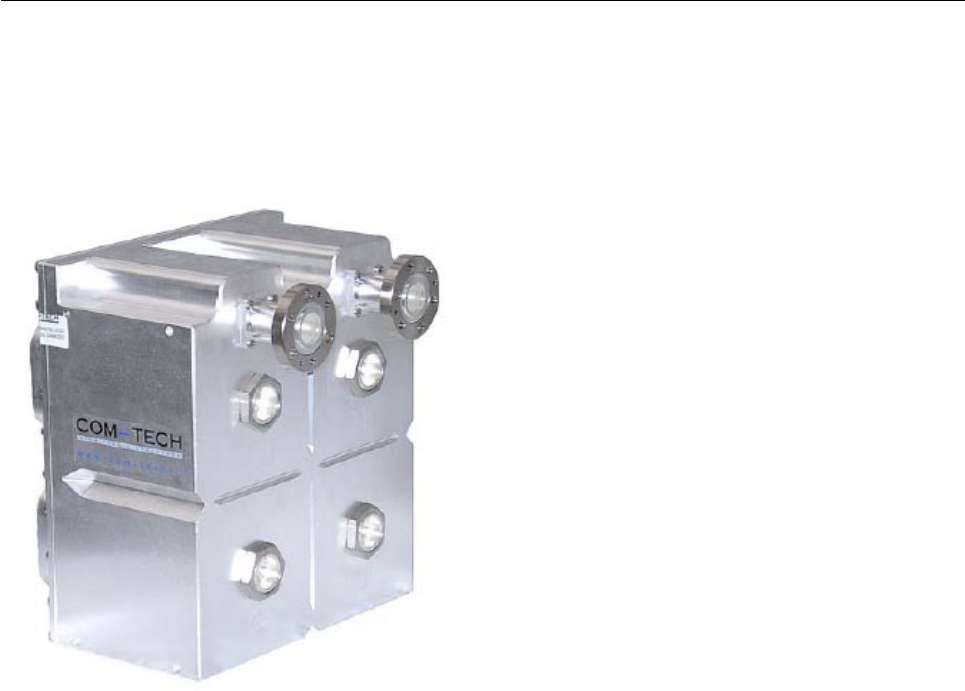
3kW UHF BANDPASS FILTER Code 06668
FEATURES
- UHF 3kW analog TV output filter
- 3D electromagnetic CAD exclusive design
- 4 poles elliptical response;
two transmission zeros for IMD suppression
- Foreshorten combline resonators structure;
iris couplings with fine bandwidth regulation
- High selectivity and low loss (Typ. 0.22dB @
V.C. Ch. 69G)
- Exclusive thermal compensation technology
providing high temperature stability (< 4kHz / K)
- Very compact, lightweight (9.1kg) and extremely
reliable
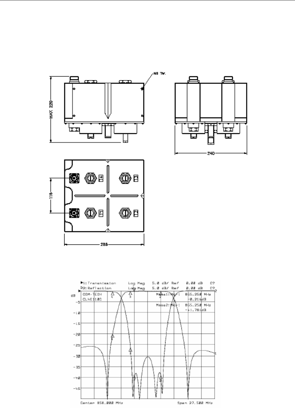
SPECIFICATIONS
Frequency Range 474 - 862MHz Selectivity* > 40dB @ V.C. -5.5 / +11MHz
> 25dB @ V.C. -11 / +16.5MHz
Max Input Power 3kW Analog TV Temperature Stability < 4kHz / K
Insertion Loss* < 0.26dB @ V.C. Ch. 69 Connectors° 7/8 Female
< 0.24dB @ V.C. Ch. 21 Weight (Approx) 9.1kg
Return Loss > 28dB Operating Temp. -10 to +50°C
Group Delay Variation < 30ns
Bandwidth 6 to 8MHz
(* Values referred to G Standards) (° See options table below)
AVAILABLE OPTIONS
A SMA Output Monitor Probe B SMB Output Monitor Probe
E 7/16 Female Connectors I EIA 1+5/8 Flange Connect.
J EIA 1+5/8 Socket Connect.
120
MECHANICAL LAYOUT
CURVE RESPONSE