User Manual
Pro
d
Mod
ELS
P
to 2
M
mod
u
ELS
P
Ame
r
can
b
E
l
No
1
2
3
4
5
6
7
8
9
10
11
12
13
14
15
16
17
18
19
20
21
d
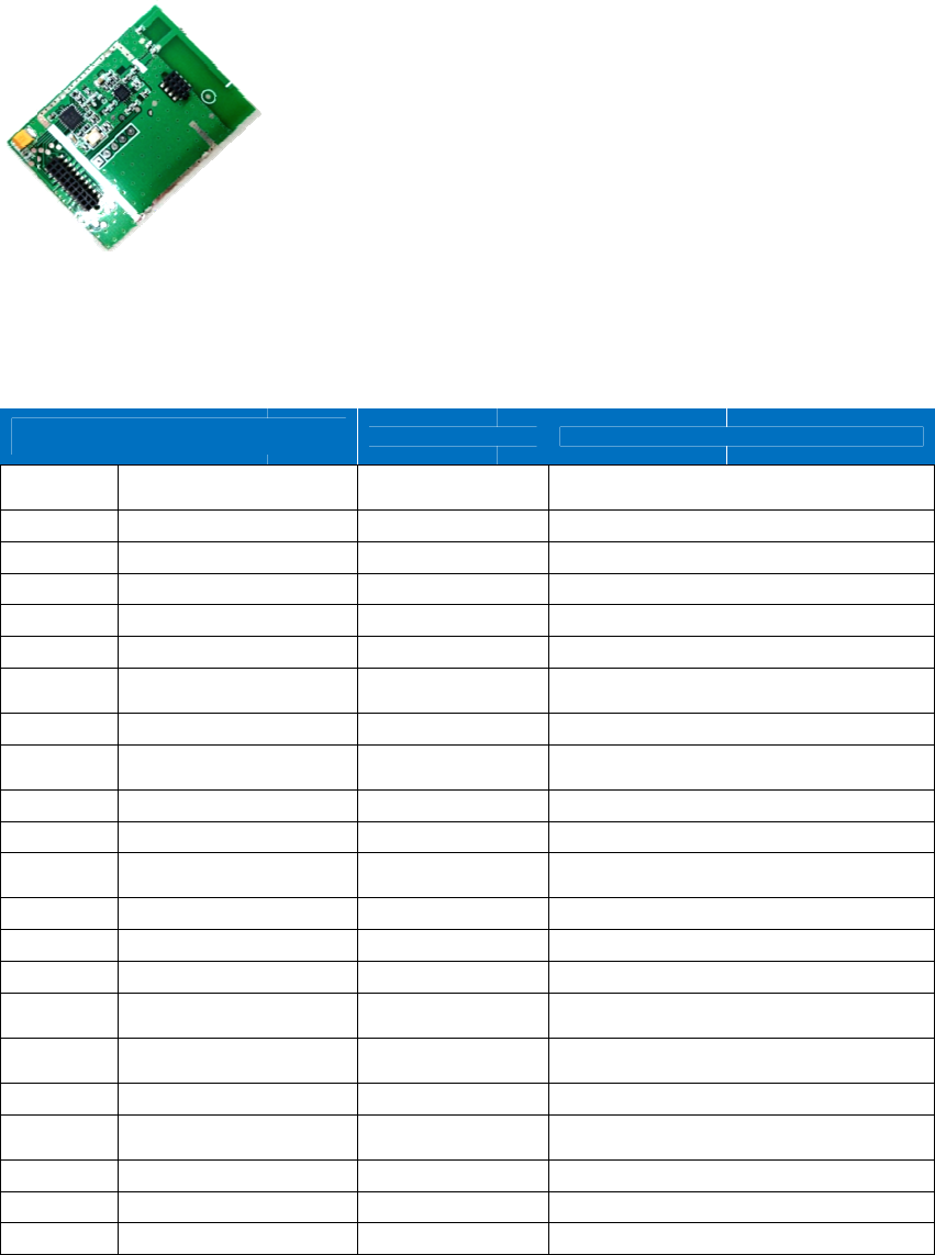
uct Name:EL
el No.: EL
S
P
01 is a 2.4GH
z
M
bps. The high-
u
le has been m
a
P
01 is Norway-i
r
ica, it's max tr
a
b
e increased b
y
l
ectrical
.
Pa
r
R
F
A
V
O
p
Pr
o
Int
e
P
o
C
o
M
e
Tr
a
R
a
Tu
E
m
R
e
C
o
E
m
R
e
R
S
An
O
p
O
p
St
o
EL
S
S-Module-01
S
P01
z
SMD wireless
performance o
n
a
ss produced s
mported from
N
a
nsmitted powe
r
y
10dB. Also, it'
s
param
e
r
ameters name
F
chip
V
and LNA Ch
i
p
erating frequ
e
o
duction tech
n
e
rface
o
wer supply
o
mmunication
e
asured dista
n
a
nsmitted po
w
a
te
rn-off current
m
ission curren
e
ceive current
o
mmunication
m
ission Len
g
e
ceive Lengt
S
SI supported
tenna
p
erating Tem
p
p
erating Humi
d
o
rage temper
a
S
P01 R
F
module with fu
n
n
board antenna
moothly, and c
a
N
ordic. Equippe
d
r
is up to 7dBm
s
small size is c
o
e
ters
P
N
i
p
R
e
ncy 2
4
n
ology l
e
2
x
1
.
level 0
.
n
ce 1
0
w
er ≤
1
2
5
1
.
t 3
5
2
0
interface S
g
th S
1
~
h S
1
~
N
3
.
A
p
erature
-
d
ity
3
a
ture
-
F
Modul
e
n
ction for recei
v
is included in
M
a
n be used for
v
d
with 20dBm
p
(conform to F
C
o
nvenient for e
m
arameter
rf24l01P
R
FX2401
4
04~2478 M
H
e
ad-free, SMT
x
10x2.54mm
.
9~3.6V DC
.
7VCC~5V
0
0m+
1
0dBm
5
0K~2Mbps
.
0uA
5
mA
0
mA
PI
ingle Data Pa
~
32 Bytes
ingle Data Pa
~
32 Bytes
onsupport
.
0dBi PCB PI
F
ntenna
-
10℃~+40℃
3
5﹪~95﹪R
H
-
40℃~+125
℃
e
User
M
v
ing and transm
M
odule, which i
s
v
arious applicat
i
p
ower amplificat
C
CID and CE ce
m
bedded devel
o
Note
Nordi
c
Rfaxi
s
H
z
SMT
Note:
perm
a
VCC i
n
Norm
a
witho
u
Cond
u
3 leve
nRF2
4
level
Max r
a
cket 3 leve
cket 3level
Supp
o
F
A
H
℃
M
anual
itting. It has a s
m
s
accurate at i
m
i
ons scenarios.
ion chip of RF
X
rtification) and
t
o
pment.
c
s
Module will b
e
a
nently, if the
v
n
dicates sup
p
a
l Mode(Sunn
y
u
t interference
u
cted Emiss
i
l adjustable(
m
4
L01P set to
p
a
te up to 10M
b
l FIFO
FIFO
o
rt simple pac
k
m
all size, and
h
m
pedance matc
h
The nRF24LO
1
X
2401 chip imp
o
t
he receiving s
e
e
damaged
v
oltage is ove
p
ly voltage
y day, circu
m
e
)
i
on Test
m
odulated via
f
p
ower down,
C
b
ps
k
et loss only
h
igh rate up
h
ing. This
1
chip in
o
rted from
e
nsitivity
r 3.6V
m
stance
f
irmware)
C
E low
22 Receive sensitivity -95dBm 1000kbps 0.1% BER
23 More details please refer to chip manual.
Interface specifications:
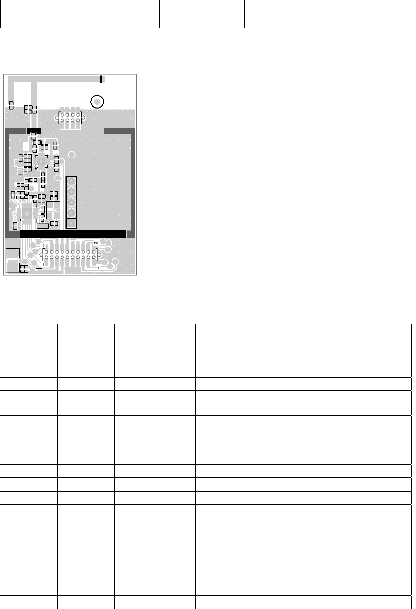
PCB Specification:
32x48.5x1.0mm
Pin Name Pin Direction Use
1 RF_SCK Input Module SPI Bus Clock
2 RF_CSN Input Module CS PIN
3 RF_CE Input Module control PIN
4 V_NRF Power supply should be between 1.9-3.6V
5 GND Ground, connect to Power ground
referenced
6 GND Ground, connect to Power ground
referenced
7 GND Ground, connect to Power ground
referenced
8 N/A Not Connected
9 N/A Not Connected
10 N/A Not Connected
11 N/A Not Connected
12 N/A Not Connected
13 N/A Not Connected
14 N/A Not Connected
15 N/A Not Connected
16 RX_EN LNA enable feet, high level effective
LNA
17 TX_EN PA enable feet, high level effective
PA
18 RF_IRQ Output Module interrupt signal output, low level
effective
19 RF_MISO Output Module SPI data output PIN
20 RF_MOSI Input Module SPI data input PIN
*Please refer to Nordic authority《Nrf24l01P Datasheet》for PIN definition of module,
software driver and communication protocol.
Notice
No Category Notice
1 Static
High frequency analog device
Avoid touching components on module if possible, since the
high frequency analog device features electrostatic susceptibility
2 Soldering Electric soldering iron must be well connected to ground when
soldering
3 Power supply
Power supply quality influence on module performance, please
insure the power supply will not appear big ripple to avoid dither
in power supply.
4 Ground
Module ground apply single point grounding. It's recommended
to use ohm inductance or 10mH inductance and set it apart from
reference ground of other circuit in other part.
5
Antenna
Mounting structure of module antenna influence module
performance. Please insure little noise interference around
antenna. Note: Antenna must not mount in metallic shell,
otherwise the transmission distance be weakened greatly.
6 Interference
If there are different frequency modules inside one product, the
frequency should be well programmed to reduce the influence of
harmonic interference and intermediation interference
7 Oscillator
If there is oscillator close to the PCB in which module mount,
please increase the distance between oscillator and PCB if
possible.

Typical Circuit
Note:
1. IRQ is a Interrupt Pin, which can be used to activate SCM to achieve quick
response.IRQ could be unconnected to obtain interruption status by SPI(It' not
recommended because of the low efficiency. And it will influence Power
Consumption.)
2. CE can be connect to high voltage level for a long term, in this way write register must be
set to POWER DOWN mode first.
3. Truth-value table for relationship between TX_EN and RX_EN as shown:
MCU

Driver Statement
1. IC nRF24L01P+RFX2401 is adopted in this module, it's driving means is same as
nRF24L01P, user can operate ELSP01 in accordance with manual for chip
nRF24L01P.
2. Connect LNA EN to MCU, LNA=1(Opened), LNA=0(Closed)
3. If user want to achieve auto-answer, LNA should be in high level during transmit
process, to ensure interface circuit be in working state.
FAQ:
★ Communication distance is close which did not achieve specified value.
1 Obstacle
With physical characteristics of poor penetrability for
2.5GHz frequency , communication distance loss will be
increased when these is line communication failed.
2 interference source Interference from temperature, humidity and co-frequency
will increase packet loss rate.
3 Metal Place antenna inside metal shell or there is metal nearby
the antenna will cause signal attenuation.
4 RX_EN PIN RX_EN PIN in emitting devices didn't keep high level will
reduce the reception sensitivity for responding signal.
5 Parameter values
功率寄存器设置错误、空中速率设置过高(空中速率越高,
距离越近)。
POWER Parameters setting error, the speed set too high.
6 Low voltage When voltage is under 3.3V, the lower voltage, the less
transmission power.
★
Heat of module, module will be damaged easily.
1 Supply voltage Check power supply and ensure it's between 2.0V~3.6V.
Module will be damaged permanently, if the voltage is over 3.6V
2 Stability Please check power supply stability, and the power noise.
3
ESD
Please insure ESD protect circuit have been applied in
mounting process, especially LNA is a easy damaged part.
4 5V lEVEL Communication line must be in series with 1k-1.5k resistance
if use 5V electrical level.
Appendix:
Channel List
Thismodulewillbeusedondifferentdevices,andthecorrespondingChannellistwillaredifference,
Mainly,ithastwomodes:
Mode1:
Channel Trigger pipe
frequency/MHz
Date pipe
frequency/MHz
1 2456 2448
2 2458 2450
3 2460 2452
4 2462 2454
5 2469 2461
6 2471 2463
7 2473 2465
8 2475 2467
9 2478
10 2449
11 2444
12 2439
13 2434
14 2429
15 2424
16 2419
17 2414
18 2410
19 2407
20 2404

Mode2:
Channel Frequency/MHz
ZI 2464
CH1 2468
CH2 2470
CH3 2472
CH4 2474
CH5 2409
CH6 2411
CH7 2413
CH8 2415
CH9 2417
CH10 2419
CH11 2421
CH12 2423
CH13 2425
CH14 2427
CH15 2429
CH16 2431
CH17 2433
CH18 2435
CH19 2437
CH20 2439
CH21 2441
CH22 2443
CH23 2445
CH24 2447
CH25 2449
CH26 2451
CH27 2453
CH28 2455
CH29 2457
CH30 2459
CH31 2461
CH32 2463
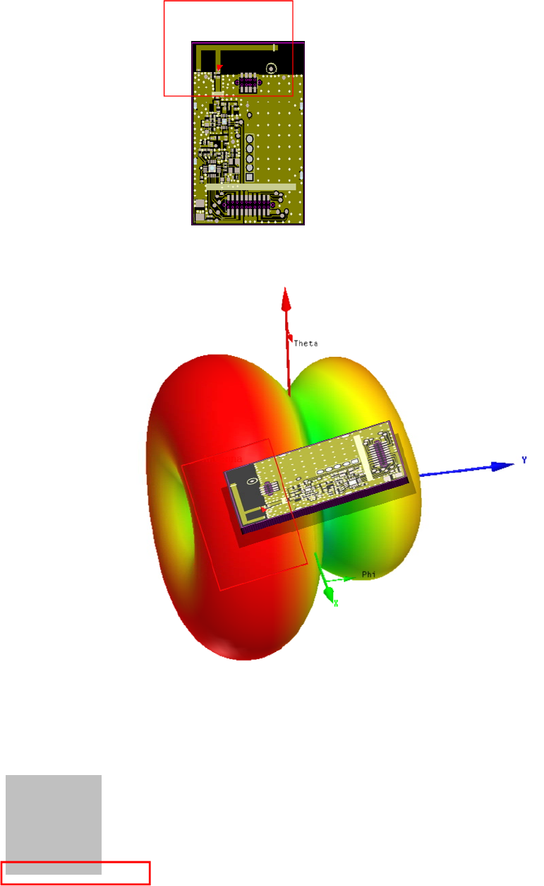
ELSP01 Antenna Specification
● PCB PIFA antenna
● GAIN:3.0dBi
Far field(f=2.4GHz)
Type Far field
Approximation enable(KR>>1)
Monitor Far field(f-2.4) [1]
Component Abs
Output Directivity
Frequency 2.4GHz
Gain. 3.0dBi
Antenna
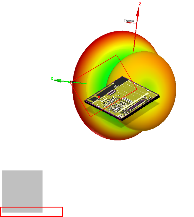
Far field(f=2.45GHz)
Type Far field
Approximation enable(KR>>1)
Monitor Far field(f-2.45) [1]
Component Abs
Output Directivity
Frequency 2.45GHz
Gain 3.0dBi
Antenna
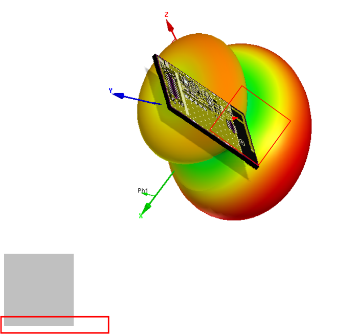
Far field(f=2.5GHz)
Type Far field
Approximation enable(KR>>1)
Monitor Far field(f-2.5) [1]
Component Abs
Output Directivity
Frequency 2.5GHz
Gain 3.0dBi
Antenna

RFeIC® is a registered trademark of RFaxis, Inc. All rights reserved.
This product document is a general list of parameters to provide information on the capabilities of this device and is subject to change without notice.
7
RFaxis, Inc. | 7595 Irvine Center Drive, Suite 200 | Irvine, California 92618 | phone: 949.336.1360 fax: 949.336.1361 website: www.rfaxis.com
Rev 2.3b
Sept '11
FCC Warning:
This equipment has been tested and found to comply with the limits for a Class B
digital device, pursuant to part 15 of the FCC Rules. These limits are designed to
provide reasonable protection against harmful interference in a residential installation.
This equipment generates, uses and can radiate radio frequency energy and, if not
installed and used in accordance with the instructions, may cause harmful interference
to radio communications. However, there is no guarantee that interference will not
occur in a particular installation. If this equipment does cause harmful interference to
radio or television reception, which can be determined by turning the equipment off
and on, the user is encouraged to try to correct the interference by one or more of the
following measures:
o Reorient or relocate the receiving antenna.
o Increase the separation between the equipment and receiver.
o Connect the equipment into an outlet on a circuit different from that to which the receiver is connected.
o Consult the dealer or an experienced radio/TV technician for help.
Caution: Any changes or modi?cations to this device not explicitly approved by
manufacturer could void your authority to operate this equipment.
This device complies with part 15 of the FCC Rules. Operation is subject to the
following two conditions: (1) This device may not cause harmful interference, and (2)
this device must accept any interference received, including interference that may
cause undesired operation.
The users manual or instruction manual for an intentional or unintentional radiator
shall caution the user that changes or modifications not expressly approved by the
party responsible for compliance could void the user's authority to operate the
equipment. In cases where the manual is provided only in a form other than paper,
such as on a computer disk or over the Internet, the information required by this
section may be included in the manual in that alternative form, provided the user can
reasonably be expected to have the capability to access information in that form.