Elmo Servo Amplifier Dbp Series Users Manual Emanudbp
SERVO AMPLIFIER DBP SERIES MAN_DBP_
DBP SERIES to the manual 99089bd7-80ef-45b2-9a4d-224e6c003172
2015-02-06
: Elmo Elmo-Servo-Amplifier-Dbp-Series-Users-Manual-539808 elmo-servo-amplifier-dbp-series-users-manual-539808 elmo pdf
Open the PDF directly: View PDF ![]() .
.
Page Count: 134 [warning: Documents this large are best viewed by clicking the View PDF Link!]

0
DBP - Rev 6/93
Rev 6/93

1
DBP - Rev 6/93
ELMO-WARRANTY PERFORMANCE
The warranty performance covers only ELMO's products and only the
elimination of problems that are due to manufacturing defects resulting in
impaired function, deficient workmanship or defective material. Specifically
excluded from warranty is the elimination of problems which are caused by
abuse, damage, neglect, overloading, wrong operation, unauthorized
manipulations etc.
The following maximum warranty period applies:
12 months from the time of operational startup but not later than 18 months
from shipment by the manufacturing plant.
Units repaired under warranty have to be treated as an entity. A breakdown
of the repair procedure (for instance of the repair of a unit into repair of
cards) is not permissible.
Damage claims, including consequential damages, which exceed the warranty
obligation will be rejected in all cases.
If any term or condition in this warranty performance shall be at variance
or inconsistent with any provision or condition (whether special or general)
contained or referred to in the Terms and Conditions of Sales set out at the
back of Elmo's Standard Acknowledge Form, than the later shall prevail and be
effective.
2
DBP - Rev 6/93
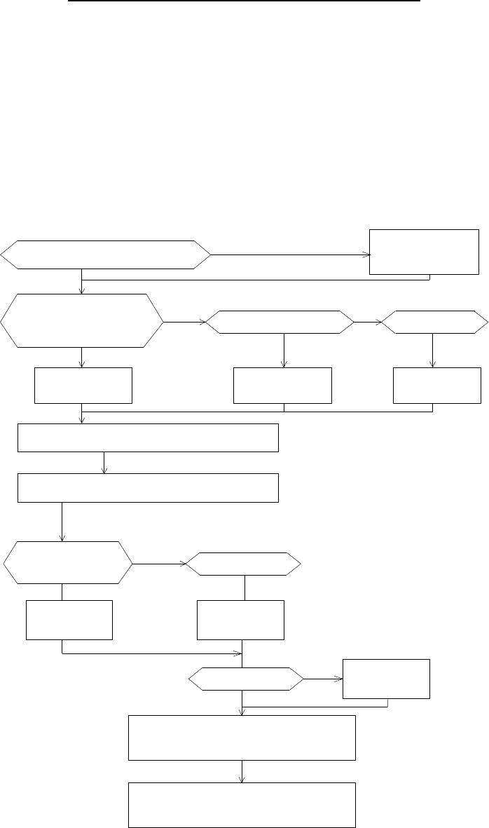
How to use this manual - Flow Chart
The DBP HARDWARE MANUAL will lead you toward a successful start-up of your
digital amplifier. Please review carefully the following flow chart and write
down the chapters that you have to follow in the right order. Only after
performing all the steps you may proceed to the software manual.
If you are a new user of the DBP, you better not skip chapters 1-4 which
will familiarize you with the product.
Read chapter 5.1
Read chapter 6 - Installation
Read chapter 7.1 - Start-Up
Read chapters
1,2,3,4
Familiar with the DBP ? no
Resolver ?
no
Read 7.2
Read chapter 8 - Applying power - Adjustments
Read chapter 9 - Summaries
Hall sensors with
Rack (R) with Elmo mother board ? Elmo enclosure ?
no no
Panel (H) version or Rack (R)
w/o Elmo mother board ?
Terminals
Read chapter 5.3
Terminals
Read chapter 5.2
Terminals
optical encoder ?
Read 7.3
Adding velocity loop ? Read Appendix B
yes
3
DBP - Rev 6/93
TABLE OF CONTENTS
1.Description ................................ .......................... 7
2. Type Designation ................................ ................... 8
3. Technical Specification ................................ ............ 9
3.1 Digital I/O specification ................................ ... 10
3.2 Analog input specification ................................ .. 13
3.3 Sensors specification ................................ ....... 14
3.3.1 Encoder ................................ ............. 14
3.3.2 Resolver ................................ ............ 14
3.4 Communication ................................ ............... 16
3.4.1 RS232 Configuration ................................ . 16
3.4.2 RS485 Configuration ................................ . 16
3.5 Battery backup ................................ .............. 16
3.6 Performance ................................ ................. 16
4. System Operation ................................ ................... 18
4.1 RS485 and Checksum Protocol ................................ . 18
4.2 Current Control ................................ ............. 18
4.2.1 Current feedback, Current feedback multiplier (CFM) and
Current loop ................................ ............... 19
4.3 Digital current limits ................................ ...... 20
4.3.1 Time dependent peak current limit ................... 20
4.4 Digital position and speed control .......................... 21
4.5 Operation of the shunt regulator ............................ 25
4.6 Commutation signals format ................................ .. 26
4.7 Protective functions ................................ ........ 27
4.7.1 Short circuit protection ............................ 27
4.7.2 Under/over voltage protection ....................... 27
4.7.3 Temperature protection .............................. 27
4.7.4 Internal power supply failure ....................... 27
4.7.5 Loss of commutation feedback ........................ 27
4.7.6 Low back-up Battery voltage ......................... 27
5. Terminal Description ................................ ............... 33
5.1 Terminals for Horizontal and Rack mounting versions ......... 33
5.2 Mother Boards terminals (MBA-DBP/3U and MBA-DBP/6U) ......... 43
5.3 Terminals for DBP mounted in ENCD. .......................... 54
5.4 Communication Port Connector ................................ 64
4
DBP - Rev 6/93
6. Installation procedures ................................ ............65
6.1 Mounting................................ .....................65
6.2 Wiring................................ ....................... 65
6.3 Load inductance................................ ..............66
6.4 AC power supply................................ ..............66
6.5 Wiring diagrams................................ ..............67
6.5.1 Motor's windings ................................ .....67
6.5.2 AC power wiring ................................ ......68
6.5.3 Hall sensors wiring ................................ ..77
6.5.4 RS232 Communication wiring ........................... 78
6.5.5 RS485 Communication wiring ........................... 79
6.5.6 Main encoder wiring ................................ ..81
6.5.7 Resolver wiring ................................ ......82
6.5.8 Auxiliary encoder wiring ............................. 83
6.5.9 Pulse/Direction signals wiring ....................... 84
7. Start - Up Procedures ................................ ..............85
7.1 Common procedures for all amplifiers types ................... 85
7.1.1 Commutation signals format ........................... 85
7.1.2 CFM function ................................ .........85
7.1.3 Abort logic ................................ ..........85
7.1.4 Setting the auxiliary position input format ..........86
7.1.5 Selecting the communication bus ...................... 86
7.1.6 Preparing the automatic baud rate selection ..........86
7.2 Setting the main optical encoder format ...................... 87
7.3 Setting the R/D circuit ................................ ......87
8. Applying power - Adjustments ................................ .......94
Step 1 - Applying Power ................................ .....94
Step 2 - Establishing the communication ..................... 95
Step 3 - Checking the feedback elements ..................... 95
Step 4 - Adjusting the current limits ....................... 95
Step 5 - Latch mode of the protective functions .............96
Step 6 - Connecting the Motor ............................... 96
9. Tables and Summaries ................................ ...............97
9.1 Display diagnostics ................................ ..........97
9.2 Summary of DIP switches ................................ ......98
Appendix A - Current loop response ................................ .....99
5
DBP - Rev 6/93
Appendix B - Adding a velocity feedback ............................... 101
Appendix C - Differential amplifier connection ........................ 102
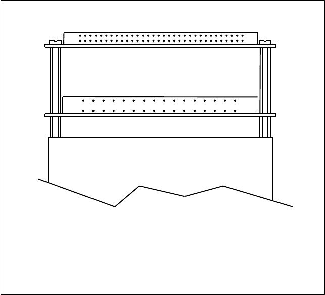
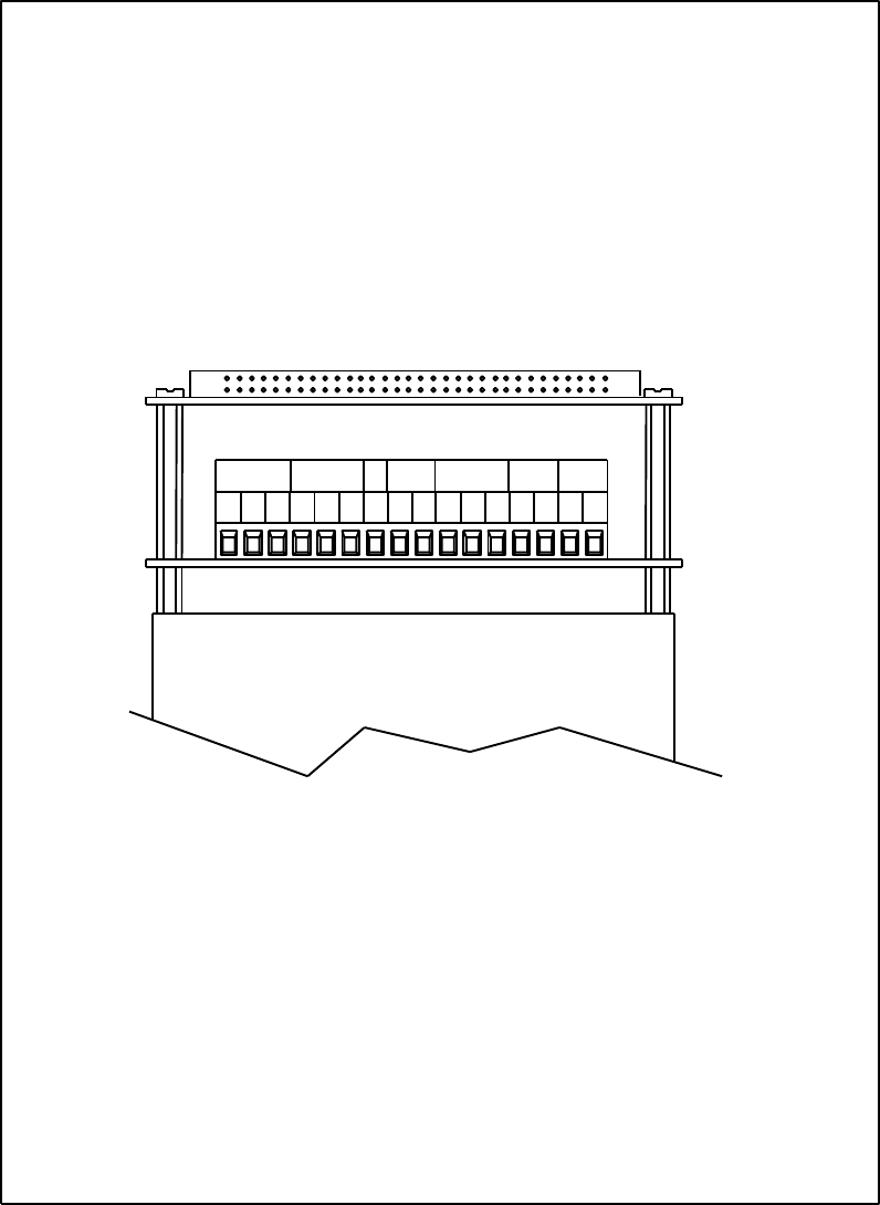
DIMENSIONAL DRAWINGS ................................ ................... 103
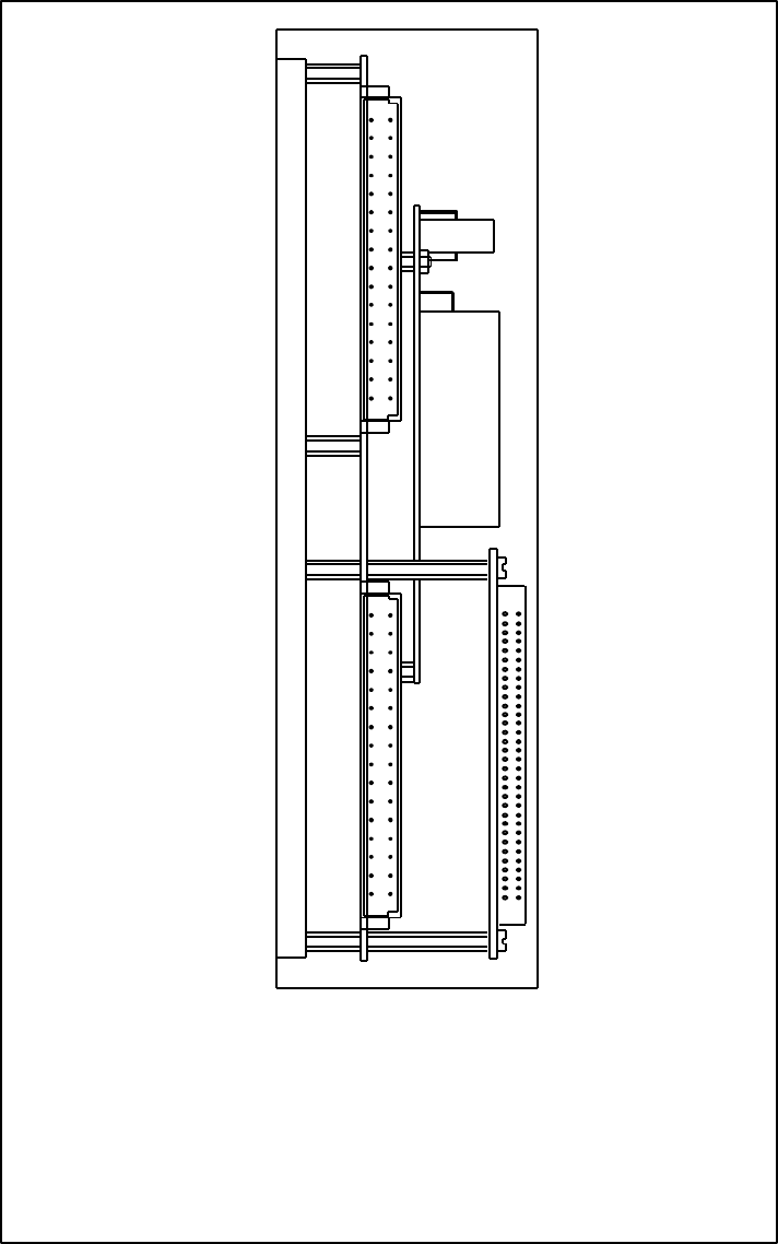
PANEL (H), DBP1 ................................ .................. 104
PANEL (H), DBP2 ................................ .................. 107
PANEL (H), DBP3 ................................ .................. 110
PANEL (H), DBP4 ................................ .................. 113
PANEL (H), DBP6 ................................ .................. 116
RACK 3U/13T ................................ ...................... 119
RACK 3U/20T ................................ ...................... 122
RACK 6U/14T ................................ ...................... 125
RACK 6U/21T ................................ ...................... 128
ENCD - 3U/... ................................ .................... 130
ENCD - 6U/... ................................ .................... 131
EXTERNAL SHUNT RESISTOR ................................ .......... 132
List of ELMO Service Centers ................................ ........... 133

6
DBP - Rev 6/93
1.Description
The DBP series are digital, full wave, three phase servo amplifiers designed
for high performance brushless servo motors in the range of up to 7KW. They
utilize power MOSFETs and Surface Mounting Technology which contribute to its
high efficiency and compact design. The DBP operates from a single AC supply
(either single or three phase) and, when using the galvanic isolation option,
it can be connected directly to the Mains.
The DBP is constructed from two main PCBs mounted on a heat sink plate. The
lower board contains the rectifying bridge, the power switching transistors
which drive the motor, terminals for the power stage, the switch mode power
supply, the protection logic and commutation logic. The upper PCB is the
Digital Control Board (DCB) which contains the digital control logic, terminals
for the control stage, D-type connector for the communication and a 4-digit
display.
The DBP requires a position sensor in order to enable its operation. It can
be either a Resolver or a combination of an optical encoder and Hall effect
sensors. When using a Resolver, a small interface card is mounted on top of the
DCB.
The DBP is available in either panel version or rack version with two DIN
41612 connectors. The rack version can be fitted in a panel mount enclosure
(ENCD-3U or ENCD-6U), that is specially designed for a simple hook-up
procedure.
The amplifiers are fully protected against the following faults:
* Under/over voltage
* Shorts between the outputs or between the outputs to ground.
* RMS current limit.
* Insufficient load inductance.
* Loss of commutation signals.
* Excess temperature.
* Excess position error.
Analog Section Standard Features:
* Single AC supply (single or three phase)
* Zero Deadband.
* Motor current monitor.
* Motor speed monitor.
* Extra differential operational amplifier.

7
DBP - Rev 6/93
* Standard commutation sensors: Hall effect sensors or a Resolver.
* Galvanic isolation of the control stage - option.
Digital Section Standard Features
* Accepts motion commands via RS232 or RS485
* Buffering for pipe lining instructions prior to execution
* Battery-backed RAM for storing user programs and parameters
* Conditional statements for controlling program execution real- time.
* Programmable time and position trip points
* Variables for entering and changing system parameters
* 5 Uncommitted inputs
* 2 uncommitted high speed inputs.
* 10 Uncommitted outputs
* Arithmetic and logic functions for manipulating parameters
* Digital filter with programmable gain, damping and integrator
* Error handling, end of travel, emergency stop, status reporting.
* 0-600,000 quadrature counts/second speed range
* One analog input - 11 bit resolution
* Master/slave operation with programmable following ratio (master information
from an optical encoder or from Pulse and Direction inputs)
* Dual-loop capability
* Adjustable continuous and peak current limits
* 4-digit display for diagnostics.
2. Type Designation
R - Resolver
E - Optical encoder + Hall sensors
I - Isolation *
O - Off line:
Rated continuos current
Max. operating AC voltage
R - Rack mounting
H - Panel mounting
DBP F- 24 / 270 R R O
DBP series amplifier
Fan cooling required for full rating Isolation + Inrush current limit

8
DBP - Rev 6/93
3. Technical Specification
Type AC Supply*
min max
Current
limits
Size
Panel(H)
Size
Rack(R)
Weight
(Kg)
DBP-12/135 28- 135 12/24 DBP2 3U/20T 1.4
DBP-20/135 28- 135 20/40 DBP3 6U/21T 3
DBP- 8/270 100- 270 8/16 DBP2 3U/20T 1.4
DBP-16/270 100- 270 16/32 DBP3 6U/21T 3
DBPF-12/135 28- 135 12/24 DBP1 3U/13T 0.7
DBPF-20/135 28- 135 20/40 DBP4 6U/13T 1.3
DBPF-30/135 28- 135 30/60 DBP6 6U/21T 3
DBPF- 8/270 100- 270 8/16 DBP1 3U/13T 0.7
DBPF-16/270 100- 270 16/32 DBP4 6U/13T 1.3
DBPF-24/270 100- 270 24/48 DBP6 6U/21T 3
* These are the absolute minimum-maximum AC supply voltage under any condition.

9
DBP - Rev 6/93
General
* DC output voltage is 130% of AC input voltage.
* 2KHz current loop response
* Outputs voltages of +5V/0.2A, +15V/0.1A for external use.
* Efficiency at rated current - 97%.
* Operating temperature: 0 - 50 °C.
* Storage temperature: -10 - +70 °C.
3.1 Digital I/O specification
Digital Inputs:
High/Low input definition: Vil<1V, Vih>2.4V
Maximum input voltage: 30V
Input impedance: 3-7Kohm
Input hysteresis: typ 1V.
When left open: low level.
Input threshold level can be shifted on request.
The fast inputs capture events (input voltage level
going from low to high) of less then 10 µsec duration.
Digital Outputs:
High/Low output definition: Vol<0.4V, Voh>4V
Output level: 0-5V
Recommended output current: Iol=Ioh=5mA
Maximum output current +10mA
The outputs are normally at low level.
10
DBP - Rev 6/93
13b
14b
15b
OUT 1
OUT 2
OUT 3
OUT 4
OUT 5
OUT 6
16b
17b
1b
D0 Q0 2
D1 Q1 5
D2 Q2 6
D3 Q3 9
D4 Q4 12
D5 Q5 15
D6 Q6 16
D7 Q7 19
OC VCC 20
U17
74HCT373A
+5V
2b
3b
OUT 7
OUT 8
OUT9
5a
3 2
U11A
74HCT4050
5 4
U11B
74HCT4050
7 6
U11C
74HCT4050
6a OUT10
MOTION
COMPLETE
7a
DIGITAL OUTPUTS
11
DBP - Rev 6/93
1 3
U100A
SN75C189AD
9a
LIMIT SWITCH
FORWARD
REVERSE
LIMIT SWITCH
10a 4 6
U100B
SN75C189AD
10 8
U100C
SN75C189AD
13 11
U100D
SN75C189AD
12a
HOME INPUT
ABORT INPUT 13a
18b 1 3
U102A
SN75C189AD
4 6
U102B
SN75C189AD
19b
I1
I2
I3 20b 10 8
U102C
SN75C189AD
13 11
U102D
SN75C189AD
1 3
U103A
SN75C189AD
21b
I4
I5
INDEX SLAVE
22b
4 6
U103B
SN75C189AD
15a
I6
I7 16a 10 8
U103C
SN75C189AD
DIGITAL INPUTS
12
DBP - Rev 6/93
3.2 Analog input specification
Maximum input voltage:
- When R1 (470ohm) is inserted, the absolute value of the input voltage should be
less than 5V.
- When the absolute value is higher than 5V, R1(Kohm) = 2Vi-10 should be inserted.
The µP reads always +5V.
Resolution of the digital conversion: 11 bit full scale.
Typical offset: 5 bits
470K
300
4700PF 4700PF
U1\10
VREF
4700PF
9
10 8
U8C
470k
18a
ANALOG 1 2 R1
*470k 6
5 7
U8B
DIGITAL GND
470k 1000PF
20K VREF
DIGITAL GND
300
4700PF 4700PF
U1\11
DIGITAL GND
20K 13
12 14
U8D
DIGITAL GND
10K
DIGITAL GND
INPUT
ANALOG INPUT
13
DBP - Rev 6/93
3.3 Sensors specification
3.3.1 Encoder
The encoder must be incremental with two TTL channels in quadrature and 90 °
phase shift.
High/Low input definition: Vil<1.5V, Vih>3V
Input voltage range: 0-15V
Input hysteresis 1.5V
Input impedance: 1Kohm to 5V.
Maximum frequency main encoder: 150KHz
Maximum frequency auxiliary encoder: 250KHz
Noise protection by analog and digital filters
When left open the input is internally pulled to high level.
3.3.2 Resolver
Resolver Option Feature:
* 10,12,14 and 16 bit resolution set by the user.
* Maximum tracking rate 1040 rps (10 bits).
* Velocity output.
* Encoder A, B, outputs + programmable index output.
Reference parameters:
Max. voltage: 20Vptp or 7Vrms
Minimum output voltage: 2Vrms
Max. current: 80mA
Max frequency: 20KHz outputs:
14
DBP - Rev 6/93
REMARK:
R704 - 708 ARE NOT INSTALLED IN FACTORY STANDARD SETTING.
+5v
2.49K
+5v +5v
1000P
100K
1K
7
3
2 U107
+5v +5v
1000P 1K
100
100
R707
*
22a
AY/PULSE
AY/PULSE
21a
DS5 301K
BY/DIR
BY/DIR 24a
100
100
23a
+5v +5v +5v
1000P
1000P
1K
100K
+5v
2.49K
7
3
2 U106
1K
+5v
301K
DS4
R706*
+5v +5v +5v +5v
+5V
4
5 6
U121B
1K
1000P 301K
1K
100K 11
10 13
U31D
1000P 1K
100
100
R708
*
32a
31a
INDEX
INDEX
DS6
+5v
1K
+5v+5v
1000P
100K
1K
7
3
2 U104
+5v +5v
1000P 1K
100
100
30a
29a
CH A
CH A
R704
*
301K
DS2
ENCODER INPUTS
1K
+5V
+5v +5v
1000P
100K
1K
7
3
2 U105
+5v+5v
1000P 1K
100
100
R705
*
28a
27a
CH B
CH B DS3 301K
Vref

15
DBP - Rev 6/93
3.4 Communication
3.4.1 RS232 Configuration
The RS232 is configured for 8-bit, no parity, full duplex and it will echo all
the transmissions.
Baud rates: 300,600,1200,2400,4800,9600,19200,38400,57600
No hardware handshaking is required.
3.4.2 RS485 Configuration
The RS485 is configured for 8-bit, no parity, half duplex.
Baud rates: 300,600,1200,2400,4800,9600,19200,38400,57600
No hardware handshaking is required.
3.5 Battery backup
180mAH battery that at rated operating and storage condition will last for
at least 40,000 non operating hours.
3.6 Performance
Position range: +230 quadrature counts
Velocity range: +600,000 counts/sec
Velocity resolution: 1 count/s
Acceleration range: 91 - 11.8x10 6 count/s
Acceleration resolution: 91 counts/s 2
16
DBP - Rev 6/93
COMMUNICATION
-15V
DZ13v
300
0.1MF 0.1MF
+15V
DZ13v
300
+5v
DS9
RS232-OFF
-V
1
DY
7
RA
5
GND
4 RTC 6
RY 3
DA 2
+V 8
U115
SN75155
+5v
5
2
3
4
TRANSMIT
RECEIVE
GND
+5V
RS232
7
6
T/R-
RS485 +5v 0.1MF
VCC
8
B
7
A
6
GND
5 D 4
DE 3
RE 2
R 1
U114
SN75LS176
1K
RS485-ON
R119
*
9
8
T/R+
1
TRANSMIT/
RECEIVE CONTROL
1K
RS485/RS232
R119 - LINE TERMINATION RESISTOR, USED ON BOTH ENDS OF LONG LINES. NORMALLY NOT MOUNTED.
*
* R802
* R802 - SMD RESISTOR. NORMALLY NOT MOUNTED
Notes:
120
ohm

17
DBP - Rev 6/93
4. System Operation
4.1 RS485 and Checksum Protocol
The RS485 in the DCB is configured as 8-bit, no parity, 1 stop bit, half
duplex. The following baud rates are available: 300, 600, 1200, 2400, 4800,
9600, 19200, 38400, 57600. No hardware handshaking is required.
In the RS-485, which is a Half Duplex system, all the Transmitters and all
the Receivers share the same Multidrop wire. Therefore, each character that is
transmitted on the line, is automatically received by all the Receivers. This
is an inherently "confused" way to transmit data and no "Echo" procedure can
assure reliable communication.
In order to solve this reliability problem, it is necessary to use standard
protocols procedures.
It is important to understand that using RS485 with the DCB products without
any protocol is possible. This is also the default condition whenever the RS485
is activated. However, the reliability of the communication is only assured
when activating the protocol. This is done by sending the command CK1 from the
host to the DCB.
Chapter 1.2.1 in the DCB Software manual explains the standard protocol used
and supplied by Elmo.
4.2 Current Control
The analog part of the DBP is actually a standard amplifier that operates in
current mode. However, the DCB receives continuously analog information about
the current magnitude, direction and ripple. This information is processed to
obtain digital control of the following features:
* Continuous current limit
* Peak current limit
* Time dependent peak current limit
* Current ripple
18
DBP - Rev 6/93
4.2.1 Current feedback, Current feedback multiplier (CFM) and
Current loop
Three current feedbacks are obtained by measuring the voltage drop across
current sensing resistors or by current transformers (when using the isolation
option). These three signals are synthesized and multiplexed which result in a
single voltage signal proportional to phases currents. It is then compared to
the current command. The error is processed by the current amplifier to provide
a voltage command to the PWM section.
Current loop control is obtained by op amp U21/A (current amplifier) and R4,
C1 which form a lag-lead network for current loop. The standard amp is equipped
with R4 and C1 to get optimum current response for an average motor in this
power range. These components are mounted in solderless terminals.
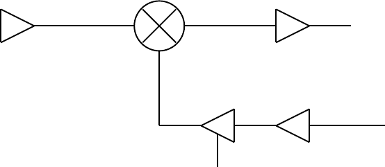
Error amplifier Current amplifier
Current feedback
CFM
x2
The amplifier is equipped with a Current Feedback Multiplier (CFM). By
turning DIP switch 2 (on the upper board of the power stage) to ON, the signal
of the current feedback is multiplied by 2 and consequently the following
changes occur:
- Current gains are multiplied by 2.
- Current monitor is divided by 2.
- Current limits are divided by 2.
- Dynamic range is improved.
- Commutation ripple is reduced.

19
DBP - Rev 6/93
This function should be activated whenever the rated current AND the peak
current of the motor are less than 20% of the amplifier rated continuous and
peak limits respectively.
Sometimes, oscillations may occur in the current loop due to the fact that
the feedback gain was multiplied. This can be resolved by substituting R4 with
a lower value.
4.3 Digital current limits
The servo amplifier can operate in the following voltage-current plane:
-Ip -Ic
+V
Ic Ip
Intermittent
zone
Continuous
zone -V
Ic - Continuous current Ip - Peak current
Fig. 4.1: Voltage-Current plane
Each amplifier is factory adjusted to have this shape of voltage-current
operating area with rated values of continuous and peak current limits. By
using the command CL(n) for the continuous and PL(n) for the peak it is
possible to adjust the current limits (continuous and peak independently) from
the rated values down to 10% of the rated values.
4.3.1 Time dependent peak current limit
The peak current duration is a programmable parameter which is also a
function of the peak amplitude and the motor operating current before the peak
demand. The user defines the maximum duration of the full amplitude peak by the
instruction PDn - n cannot be more than 2 seconds. In addition to this
definition, a digital filter is employed to ensure that the RMS value of the
current will not exceed the continuous current limit. The duration of Ip is
given by:

20
DBP - Rev 6/93
Ip - Iop
Tp = 2.2ln ----------
Ip - Ic
Iop - Actual operating current before the peak demand.
The result of this filter is that the maximum peak can last for a maximum of
2 seconds. A lower peak can last longer.
Example: A motor is driven by an DBPF-10/135 amplifier at constant speed and
constant current of 5A. What is the maximum possible duration of a 20A peak ?
20 - 5
Tp = 2.2ln -------- = 0.892 seconds
20 - 10
4.4 Digital position and speed control
The DCB accepts motion commands via an RS232 or RS485 communication line and
receives position feedback in an incremental encoder format either from an
encoder or from the resolver/digital circuit. The DCB derives the closed-loop
position error by comparing the command position and the feedback position. The
error is processed by a digital filter to yield with an analog motor command.
The analog +5 volt range motor command is then amplified by the power
amplifier.
Following is a summary of all the operating modes of the DCB and a detailed
discussion of each of them.
Control Modes
Holding Modes.
Start Modes
Program Mode
Termination Modes
Status reporting
Define origin modes

21
DBP - Rev 6/93
Control Modes
The DCB can be commanded to control the position of a motor, its torque or
its velocity using three basic control modes:
- Position Mode
- Velocity Mode
- Position Follower Mode
Position Mode
In the position mode the motor will advance a specified distance and then
stop. This distance can be represented as an absolute position (PA n) or as a
relative distance from the current position (PR n). The motion will follow a
trapezoidal or triangular profile with the acceleration (AC n) and slew
velocity (SP n) set by the user.
Velocity Mode
In the velocity mode the motor will accelerate to a specified slew speed. It
will hold this speed until a stop condition is received (see termination
modes), or a new velocity/direction is commanded.
Position Follower
It can also control the motor as a position follower of a master encoder or
a pulse and direction signals.
Holding Modes.
The holding modes describe the behavior of the system after it has stopped.
There are three holding modes:
- Servo
- Motor Off
Servo Mode
In the servo mode (SV) the system maintains stopping position by using its
control law to correct for any position errors.
Motor Off Mode
In the Motor Off mode is, the power bridge and the position control are shut
off and there no torque is generated by the amplifier. The Motor Off mode is
useful in robotics applications in the teaching mode.

22
DBP - Rev 6/93
Start Modes
There are three start modes to begin a move:
Direct command
A move can be initiated directly by a command from the host or a terminal.
Program
A move can be initiated by a command included in the user program.
Input condition
Another alternative is to have the move started by a conditional statement
specified by the user program.
Program Mode
A set of commands can be implemented as a user program to allow for
automatic and/or complex types of moves. The user may specify software
variables, conditional statements, subroutines and error routines which enable
enhanced motion control.
Termination Modes
A motion can be terminated in a variety of ways. In all but emergency
termination modes the motor will be decelerated gradually to a stop and then
will enter one of the stationary modes (Servo, or Motor Off). In a position
mode move, the motion will terminate naturally upon reaching the desired final
position. In all of the control modes the motion can be terminated by a command
from the host. An additional means of termination is from one of the local
inputs.
Activating the forward and reverse limit switch inputs can be another means
of terminating a move. Upon contacting the switch, the #[ routine will be
activated. This is a user programmed routine that should normally include a
stop command to decelerate the motor to a full stop.
There are two methods of generating an emergency stop. The first is by an
abort command from the host, and the other is by the local abort input. Upon
receipt of either of these commands the system will go immediately to its
stationary mode.
Another "unnatural" way to terminate a motion is whenever an internal
amplifier inhibit (due to one of the protections) occurs. This turns off the
power stage and the motor will decelerate to a stop by friction only. There are
two modes of handling the internal amplifier inhibit:
Latch Mode
The power stage is disabled and only a reset will release it.

23
DBP - Rev 6/93
Auto restart
The power stage inhibit will automatically be released upon clearing the
cause of the inhibit.
Status Reporting
Status is available to the user in several ways.
Communication
In response to the Tell Status command (TS) the DCB sends a coded message
describing the status of the amplifier.
In addition, the host may request certain information at any time. This
consists of the state of the system (GN?, ZR?, PL?, KI?), the state of the
local inputs (TI), the torque level (TT), the current motor position (TP), the
current motor velocity (TV) and the reason for a stop condition (TC).
Refer to the DCB Software Manual for further details.
Hardware signal
Motion complete signal
This output will go to high when motion is complete.
Inhibit output
Whenever the amplifier is inhibited, this open collector output goes to low.
When using Elmo's mother boards a potential free relay replaces the open
collector output.
4-digit display
Whenever a fault occurs, a fault message will be displayed for easy visual
information. See chapter 9.1 for a summary of all amplifier's fault
indications.
Define origin modes
The origin is that location at which the absolute position of the motor
equals zero. This special location may be defined in two ways. First, the user
may send a command (DH) which defines the current motor position to be the
origin. The alternate method is to request the DCB to perform the homing
sequence by commanding HM.

24
DBP - Rev 6/93
4.5 Operation of the shunt regulator
A shunt regulator is included in the power supply section of the DBP. The
shunt regulator is a switching type, wherein dissipative elements (resistors)
are switched across the DC bus, whenever the voltage reaches a predetermined
level (Vr). The function of the shunt regulator is to regulate the voltage of
the DC bus during the period of motor deceleration, when there is a net energy
outflow from the motor to the amplifier. The amplifier handles this reverse
energy just as efficiently as it provides energy to the motor, hence, most of
the energy is passed through the amplifier to the power supply, where the
returning energy charges the filter capacitors above their normal voltage
level, as determined by the AC incoming voltage.
When the capacitors charge-up reaches the predetermined voltage level (Vr),
the shunt regulator begins its regulating action. The bus is regulated to this
range until regeneration ceases.
All the double Eurocard size amplifiers are equipped with two outputs for
connecting an external shunt resistor , hence increasing the power dissipation
capability.
SHUNT specifications
Type Reg.
Voltage
(Vr)
Internal
Reg.
Current (A)
External Reg.
Current (A)
DBP-12/135 193 13 N/A
DBP-20/135 193 26 21
DBP-8/270 383 8 N/A
DBP-16/270 383 16 12
DBPF-12/135 193 13 N/A
DBPF-20/135 193 26 N/A
DBPF-30/135 193 26 21
DBPF-8/270 383 8 N/A
DBPF-16/270 383 16 12
DBPF-24/270 383 16 12
25
DBP - Rev 6/93
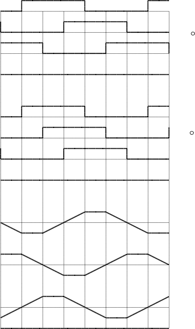
4.6 Commutation signals format
300 60 120 180 240 300 360 600
(0)
(360)
300 60 120 180 240 300 360 600
(0)
(360)
300 60 120 180 240 300 360 600
(0)
(360)
A
B
C
A
B
C
0
0
0
+
-
+
-
Vac
Vba
Vcb
60 FORMAT (120)
30 FORMAT
MOTOR BEMF
+
-
26
DBP - Rev 6/93
4.7 Protective functions
All the protective functions except "Low Back-up Battery Voltage" activate
an interrupt to the main processor which inhibits the power bridge and disable
current flow to or from the motor. The user can interrogate the processor in
order to verify the cause of the inhibit. An indication of the fault will
appear on the display. The following protections are processed by the DCB:
4.7.1 Short circuit protection
The amplifier is protected against shorts between outputs, or either output
to ground, or either output to the positive supply line.
4.7.2 Under/over voltage protection
Whenever the DC bus voltage is under or over the limits indicated in the
technical specifications, the amplifier will be inhibited.
4.7.3 Temperature protection
Temperature sensor is mounted on the heatsink. If, for any reason, the
temperature exceeds 85°C the amplifier will be inhibited. The amplifier will
restart when the temperature drops below 80 °C. The user can always interrogate
the DCB about the heatsink temperature by using the command T?.
4.7.4 Internal power supply failure
In any case that the sum of the internal power supplies is below 13V or its
difference higher than 1V, the amplifier will be inhibited.
4.7.5 Loss of commutation feedback
Lack of either of the commutation signals will inhibit the amplifier.
4.7.6 Low back-up Battery voltage
When the battery voltage goes below 2.4V the DCB will send a message on the
communication line and will display "BATT" on the display.
27
DBP - Rev 6/93
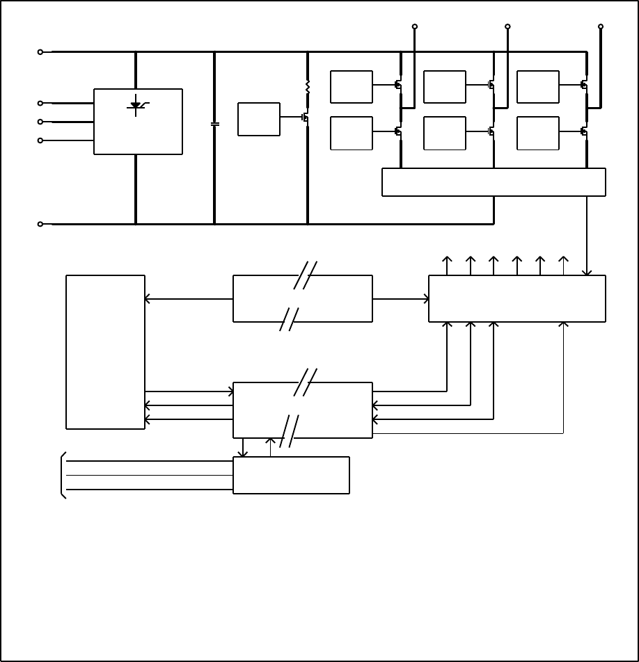
MOTOR OUTPUTS
+VS
AC
AC
SHUNT D1 D2 D3
D6D5
CURRENT SENSING
D4
CONTROL
RECTIFING,
CURRENT
INRUSH LIMIT
AC
POWER
COMMON
D5 D6
COMMUTATION
CURRENT PROCESSING
D1 D2 D3 D4
SUPPLIES
SMPS
SUPPLIES
CONTROL
PROTECTIONS
CURRENT FEED BACK
PWM SIGNALS
"HALLS" SIGNALS
ISOLATION
PWM SIGNAL
CURRENT FEED BACK
PROTECTIONS
HA
HB
HC
"HALL" SIGNAL
PROCESSING
DBP 3U - BLOCK DIAGRAM
28
DBP - Rev 6/93
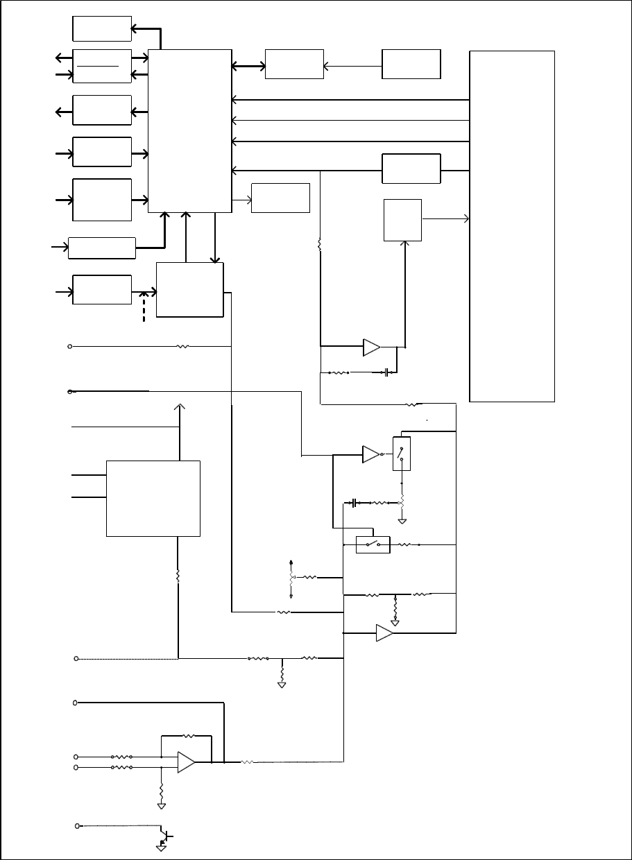
RS232
Display
RS485
Outputs
Buffers Master
Processor TEMP SIGNAL
SHORT SIGNAL
UNDER / OVER - SIGNAL
Current
Feedback
Inputs
Buffer
Aux
Buffer
Encoder
Encoder
Analog in
Position
ProcessorBuffer
option
MOTOR COMMAND
Current
limits
TACH INPUT (OPTION) R7
10K
100K
A
PWM
A
option
R6
C2
100K 100K
R5
619K
VELOCITY/ CURRENT MODE
+V
-V
OFFSET
OPTION 1M
R800
100K
POWER
STAGE
-
+
R4
100K
C1
.01UF
ERROR AMPLIFIER
100K
MEMORY BATTERY
BACK UP
R3
R2
10K
10K
DCB BLOCK DIAGRAM
RESOLVER
OPTION
VELOCITY
FEEDBACK
SIGNAL
1K
(TACH OUTPUT WITH RESOLVER OPTION)
ENCODER OUTPUTS
TO POSITION
PROCESSOR
CURRENT
AMPLIFIER
INH. OUT 10MA/30V
29
DBP - Rev 6/93
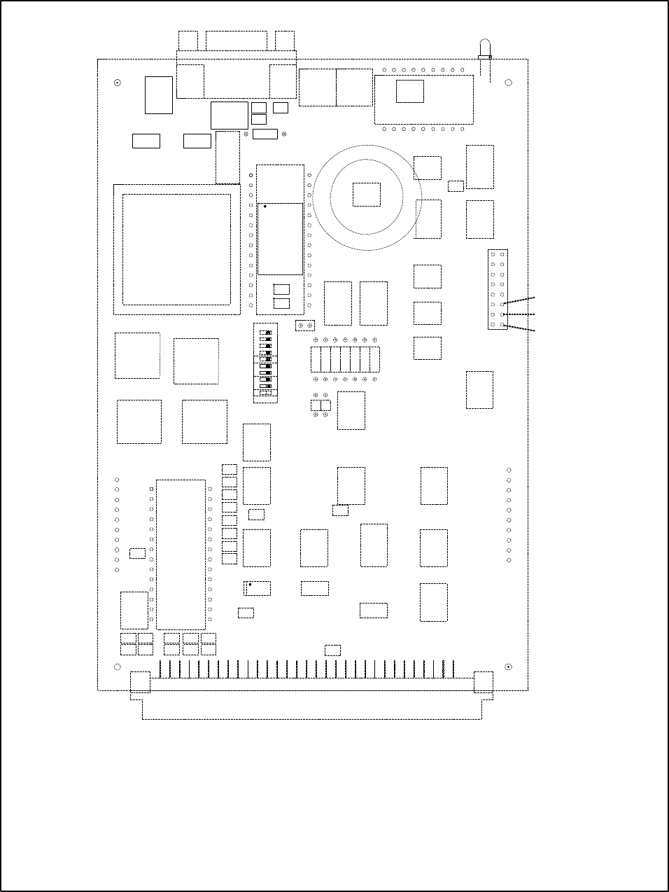
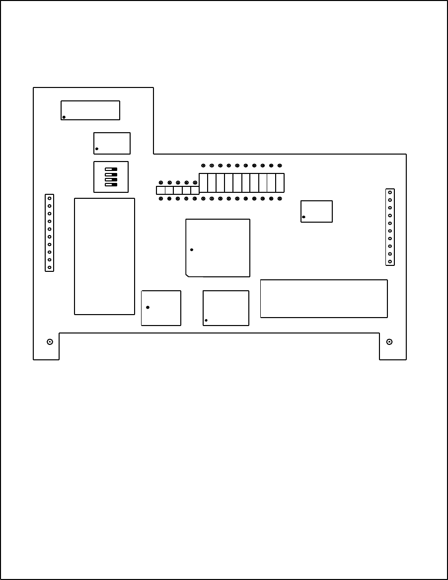
DCB COMPONENTS LAYOUT
L1
T1T2
JC
U120
U114
N80C196KB-12
U115
U123
Y1
R713
R712
R119
R802
U130
U25
U22
R566
U108
U109
JP
U27
U112
U113
U28
C313
C312
JE
DS
OFF ON
U5
U17
U10
U101
U7
U18
12
34
56
78
9
R R
C1C2 U21
U26
R R R R
U20
JPR
U9 U21
U29
U11
C139
U31
R800
R500
R501
R502
R503
R508
R509
R510
R511
U100
U103
R705
JR
506
507
R504
R505
U102 R708
706
704
C300
513
518
519
U106
R707
U107
D7 U8
U116
R
1 2 34 5 6 7
HA
HB
HC
30
DBP - Rev 6/93
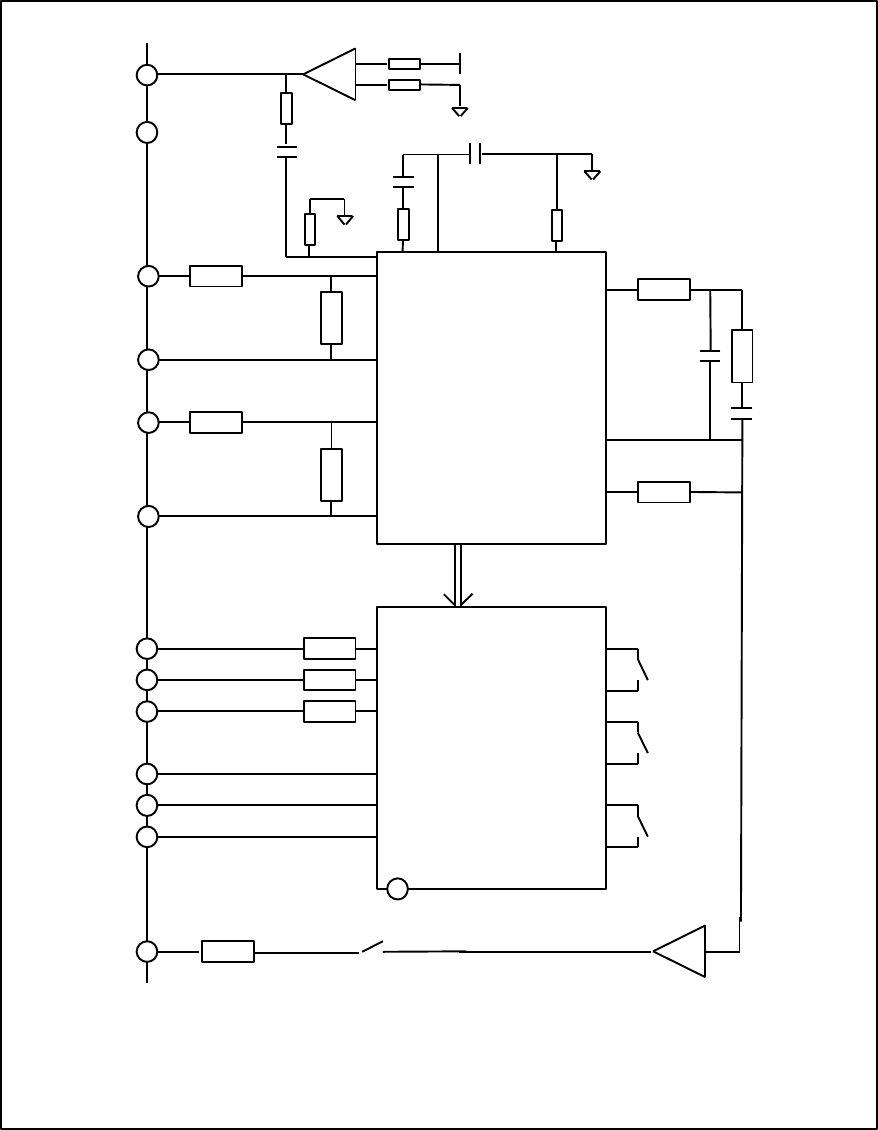
DCB RESOLVER OPTION BLOCK DIAGRAM
DS14
DS13
DS12
HALLS + ENCODER
PROCESSOR
POSITION
BITS
RESOLVER TO
DIGITAL CONVERTER
R201
R200
C68
C67
R197
Velocity feedback
DS11
HA
HB
HC
ENCODER A
ENCODER B
ENCODER I
R242
R243
R244
R193
R194
2K
2K
Ref. oscillator output
R192
+V
R228
R233
C60
C61
R196
R196
C62
SIN. INPUT
COS. INPUT
JR/1
JR/2
JR/3
JPR/10
JPR/9
JPR/8
JR/8
JR/7
JR/10
JR/9
JR/5
JR/6 Ref. osc. common
JR/4 1K
31
DBP - Rev 6/93
RESOLVER BOARD
COMPONENTS LAYOUT
U25
U24
DS2
ON
OFF 11
12
13
14
U22
60
68
67
62
61 R
192
R
200
R
197
R
195
R
196
R
201
U30
R
233
R
228
R
193
R
194
U23
U28 U29
c c c c c
JR
1
10
JPR
1
10

32
DBP - Rev 6/93
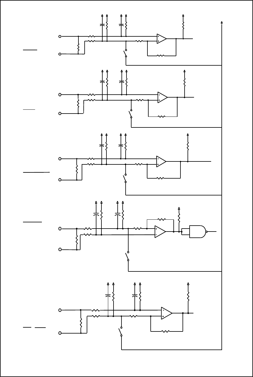
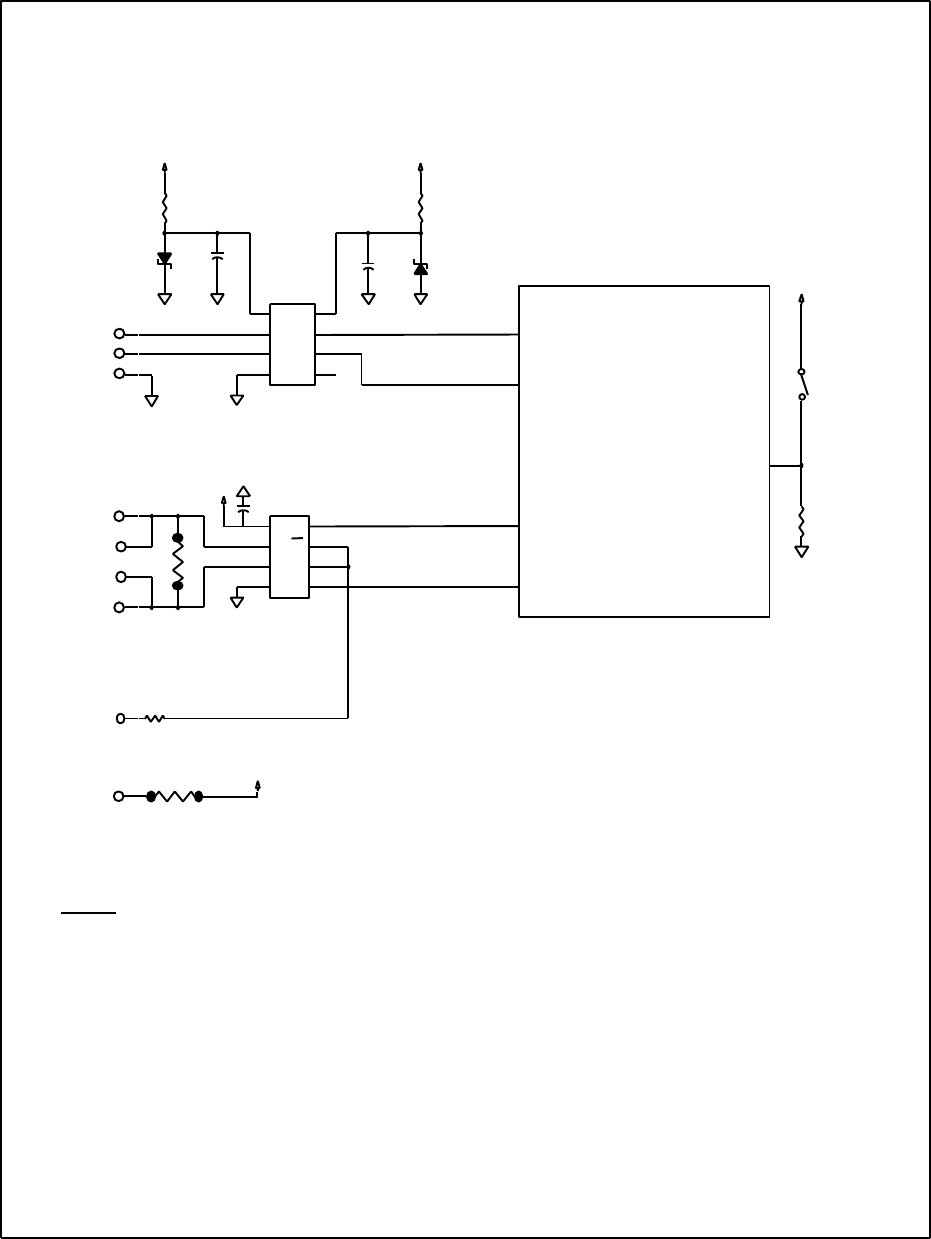
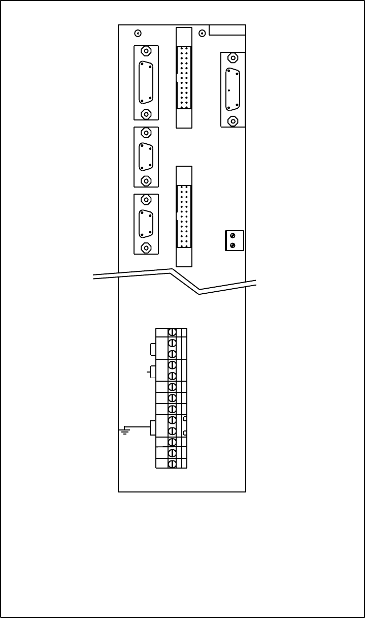
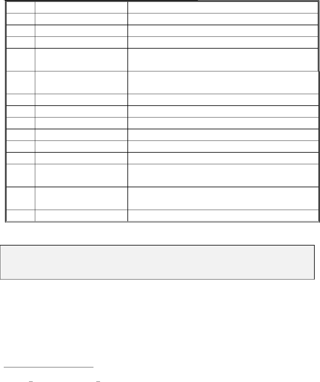
5. Terminal Description
5.1 Terminals for Horizontal and Rack mounting versions
POWER BOARD - 3U size
H R Function
1 (32a,c) Motor phase A output. With the DIN connector both pins must be
connected.
2 (30a,c Motor phase B output. With the DIN connector both pins must be
connected.
3 (28a,c) Motor phase C output. With the DIN connector both pins must be
connected.
4 (26a,c) AC supply-phase A. With the DIN connector both pins must be
connected.
5 (24a,c) AC supply-phase B. With the DIN connector both pins must be
connected.
6 (22a,c) AC supply-phase C. With the DIN connector both pins must be
connected.
7 (20a,c) DC power positive (+Vs)
8
9
(18a,c
16a,c)
DC power common
10 (14c) Hall sensor A *
11 (12c) Hall sensor B *
12 (10c) Hall sensor C *
13 (8c) +15VDC for Hall sensors supply.
14 (6c) Circuit common for the Hall sensors supply (Control common).
15 (4c) 24V common - for the fan supply only.
16 (2c) +24VDC, 400mA for use with brushless fan
* -1V < Vil < 1V ; 2V < Vih < 30V
Source sink capability - 2mA min.

33
DBP - Rev 6/93
Power Board - 6U size - Supplies terminals
H R FUNCTION
+VS 4ac,2ac External shunt resistor connection / +VS.
NC NOT CONNECTED
SO 8ac External shunt resistor connection.
NC NOT CONNECTED
POW
COM
14ac,12ac POWER COMMON
NC NOT CONNECTED
AC 20ac,18ac AC supply-phase A. With the DIN connector all pins must be
connected.
AC 26ac,24ac AC supply-phase B. With the DIN connector all pins must be
connected.
AC 32ac,30ac AC supply-phase C. With the DIN connector all pins must be
connected.
Power Board - 6U size - Motor terminals
H R FUNCTION
HC 2c Hall sensor C *
HB 4c Hall sensor B *
HA 6c Hall sensor A *
-FAN 8c 24V common - for the fan supply only
+FAN 10c +24VDC, 400mA for use with brushless fan
MC 18ac,16ac,14a Motor phase C output. With the DIN connector all pins must
be connected.
MB 26c,24ac,22ac Motor phase B output. With the DIN connector all pins must
be connected.
MA 32ac,30ac,28c Motor phase A output. With the DIN connector all pins must
be connected.
* -1V < Vil < 1V ; 2V < Vih < 30V
Source sink capability - 2mA min.

34
DBP - Rev 6/93
Control board
H & R Function Remarks
1a Output 6 *
1b Current monitor This analog output represents the actual current
in the motor. The scale (in A/V) is: Ip / 7.5
Ip - Rated peak current of amplifier.
2a Output 7 *
2b Velocity / current mode
selection
When input is left open (low level) the analog
part of the amplifier is working in current mode.
when a high level signal is applied (>2V), the
analog part of the amplifier is working as a high
gain velocity amplifier.**
3a Output 8 *
3b Motion command (+5V) This analog output represents the current command
from the position loop to the power amplifier. It
is useful for monitoring the position loop
response.
4a Circuit common
4b Circuit common
5a Fast output 9 *
5b +5V output There are several +5V terminals. The accumulative
external load should not exceed 200mA.
6a Fast output 10 *
6b Circuit common
7a Motion Complete This output will go to high when motion is
complete. *
7b +15V output 100mA.
8a Inhibit output Whenever the amplifier is inhibited, this open
collector output goes low.
8b -15V output 100mA.
* Vol<0.4V, Voh>4V, Output level: 0-5V, max output current +5mA
** Vil<1V, Vih>2.4V, Maximum input voltage: +30VDC

35
DBP - Rev 6/93
Control board - cont.
H & R Function Remarks
9a Forward limit switch This committed input activates the #[ subroutine. *
9b positive input of a
differential amplifier.
See Appendix C.
10a Reverse limit switch This committed input activates the #[ subroutine.*
10b Negative input of a
differential amplifier.
See Appendix C.
11a Circuit common
11b Output of a
differential amplifier.
See Appendix C.
12a Home switch *
12b Tachogenerator
output/input
When using the resolver option this output is the
velocity monitor with a scale of 8V for maximum
speed. See 7.3.
13a Abort input This input must be connected to high level voltage
to enable the amplifier.*
13b Output 1 **
14a Circuit common
14b Output 2 **
15a Fast input 6 This fast response input can capture events with a
duration of less than 10µs. An event is defined as
an input voltage transition from low to high. *
15b Output 3 **
16a Fast input 7 Same function as Fast Input 6 (15a). *
16b Output 4 **
17a Reset input *
17b Output 5 **
* Vil<1V, Vih>2.4V, Maximum input voltage: +30VDC
** Vol<0.4V, Voh>4V, Output level: 0-5V, max output current +5mA

36
DBP - Rev 6/93
Control board - cont.
H & R Function Remarks
18a Analog input This input is monitored by the main µP. When |Vi|
< 5V, R1=470ohm should be inserted. When |Vi|> 5V,
R1(Kohm)=2Vi-10 should be inserted. The µP always
reads a range of +5V.
18b Input 1 *
19a +5V output There are several +5V terminals. The accumulative
external load should not exceed 200mA.
19b Input 2 *
20a Circuit common
20b Input 3 *
21a Auxiliary encoder input
(Ay) or pulse input for
Pulse and Direction
mode.
21b Input 4 *
22a Auxiliary encoder
complementary input (-
Ay) or complementary
Pulse and Direction
mode
22b Input 5 or Index Input. If a homing sequence is required, the Index Input
must be connected to Input 5 *
23a Auxiliary encoder input
(By) or Direction input
for Pulse and Direction
mode
23b Resolver reference Max. voltage: 20Vptp or 7Vrms
Max current: 80mA
Max frequency: 20KHz
* Vil<1V, Vih>2.4V, Maximum input voltage: +30VDC

37
DBP - Rev 6/93
Control board - cont.
H & R Function Remarks
24a Auxiliary encoder
complementary input (-
By) or Complementary
Direction input for
Pulse and Direction
mode
24b Resolver reference
common.
The reference voltage to the resolver must be
taken from terminals 23b and 24b only.
25a +5V output There are several +5V terminals. The accumulative
external load should not exceed 200mA.
25b Cosine signal input. See 7.3
26a Circuit common For the auxiliary encoder
26b Cosine signal common. See 7.3
27a Channel B input
27b Sine signal input. See 7.3
28a Channel -B input
28b Sine signal common See 7.3
29a Channel A input
29b Circuit common For the main encoder
30a Channel -A input
30b Index output For resolver option only.
31a -Index input
31b Channel B output
32a Index input
32b Channel A output
Remark: In the following paragraphs the terminals will be related to all the
mounting types as in the following sample:
H/R-2a,E-J4/13.
38
DBP - Rev 6/93
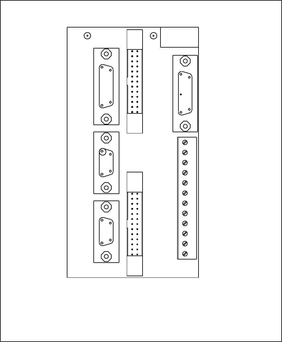
TERMINALS OF DBP
RACK VERSION - 3U SIZE
CONTROL BOARD 1
32 b
a
24
c
a
32 POWER BOARD
39
DBP - Rev 6/93
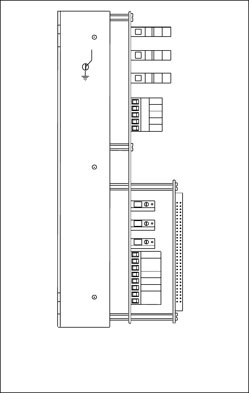
DBP - PANEL (H) MOUNTING TYPE
TERMINALS LAYOUT
EUROCARD SIZE TYPES
CONTROL BOARD
b
a
1
32
1 2 3 4
+VS
A
AC input
5 6 7 8
B C
MOTOR OUT
910 11 12 13
COM. ABC
POWER HALL
14 15 16
24
-+
SUPPLY FAN
~ ~ ~C+15
40
DBP - Rev 6/93
DBP - PANEL (H) MOUNTING TYPE
DOUBLE EUROCARD SIZE TYPE
ba1
32
M4
+FAN
-FAN
HA
HB
HC
AC
AC
AC
POW
COM.
N.C
N.C
S.O
N.C
+VS
MC
MB
MA
1
2
3
4
5
6
15
16
17
18
19
7
8
9
10
11
12
13
14
41
DBP - Rev 6/93
DBP-6U RACK TYPE
32
2C
A
32
C
A
2
A
J1
J3
POWER
POWER
CONTROL
CONNECTORS
ba1
32

42
DBP - Rev 6/93
5.2 Mother Boards terminals (MBA-DBP/3U and MBA-DBP/6U)
Use: For all DBP amplifiers (3U/6U size) with Resolver or optical encoder
feedback. The encoder outputs are driven by line drivers to improve noise
immunity.
Termination: Screw type terminals for the power and D-type connectors for the
signals.
POWER TERMINALS FOR MBA-DBP/3U
H R Function
1 (32a,c) Motor phase A output. With the DIN connector both pins must be
connected.
2 (30a,c Motor phase B output. With the DIN connector both pins must be
connected.
3 (28a,c) Motor phase C output. With the DIN connector both pins must be
connected.
4 (26a,c) AC supply-phase A. With the DIN connector both pins must be
connected.
5 (24a,c) AC supply-phase B. With the DIN connector both pins must be
connected.
6 (22a,c) AC supply-phase C. With the DIN connector both pins must be
connected.
7 (20a,c) DC power positive (+Vs)
8
9
(18a,c
16a,c)
DC power common
10 Ground, this terminal is connecred through a screw to the rack
chassis.
15 (4c) 24V common - for the fan supply only.
16 (2c) +24VDC, 400mA for use with brushless fan

43
DBP - Rev 6/93
POWER TERMINALS FOR MBA-DBP/6U
Terminal Function
M1 Motor phase A output.
M2 Motor phase B output.
M3 Motor phase C output.
GND Ground. This terminal is connected to the ENC chassis.
AC AC supply-phase A.
AC AC supply-phase B.
AC AC supply-phase C.
COM DC power common
VS DC power positive
SO Auxiliary shunt output, for external shunt resistor.

44
DBP - Rev 6/93
Signals connector - J1 (MBA-DBP/3U and MBA-DBP/6U)
Pin Function Remarks
1 Channel A input
2 Channel -A input
3 Channel B input
4 Channel -B input
5 -Index input
6 Index input
7 +5V output There are several +5V pins. The accumulative
external load should not exceed 200mA.
8 +15V output There are several +15V pins. The accumulative
external load should not exceed 100mA.
9 Circuit common
Signals connector - J2 (MBA-DBP/3U and MBA-DBP/6U)
Pin Function Remarks
1 Resolver reference Max. voltage: 20Vptp or 7Vrms
Max current: 80mA
Max frequency: 20KHz
2Resolver reference
common.
The reference voltage to the resolver must be
taken from pins 1 and 2 only.
3 Cosine signal input. See 7.3
4 Cosine signal common. See 7.3
5 Sine signal input. See 7.3
6 Sine signal common See 7.3
7 +15V output There are several +15V pins. The accumulative
external load should not exceed 100mA.
8 -15V output There are several -15V pins. The accumulative
external load should not exceed 100mA.
9 Circuit common

45
DBP - Rev 6/93
Signals connector - J3 (MBA-DBP/3U and MBA-DBP/6U)
Pin Function Remarks
1positive input of a
differential amplifier.
See Appendix C.
2Negative input of a
differential amplifier.
See Appendix C.
3Output of a
differential amplifier.
See Appendix C.
4 Circuit common
5 Analog input This input is monitored by the main µP. When |Vi|
< 5V, R1=470ohm should be inserted. When |Vi|>
5V, R1(Kohm)=2Vi-10 should be inserted. The µP
always reads a range of +5V.
6 Circuit common
7 Circuit common
8 Current monitor This analog output represents the actual current
in the motor. The scale (in A/V) is: Ip / 7.5
Ip - Rated peak current of amplifier.
9 Circuit common
10 +5V output There are several +5V pins. The accumulative
external load should not exceed 200mA.
11 +15V output There are several +15V pins. The accumulative
external load should not exceed 100mA.
12 -15V output There are several -15V pins. The accumulative
external load should not exceed 100mA.
13 Channel B output
14 Channel A output
15 Index output For resolver option only.
16 Not connected
17 Inhibit output Relay contact (potential free).
The relay contact is closed whenever the
amplifier is enabled. Contact rating: 0.5A, 200V,
10W.
46
DBP - Rev 6/93
Signals connector - J3 - cont.
Pin Function Remarks
18 Inhibit output Relay contact (potential free).
The relay contact is closed whenever the
amplifier is enabled. Contact rating: 0.5A, 200V,
10W.
19 Motion command (+5V) This analog output represents the current command
from the position loop to the power amplifier. It
is useful for monitoring the position loop
response.
20 Circuit common
21 Reset input *
22 Circuit common
23 Tachogenerator
output/input
When using the resolver option this output is the
velocity monitor with a scale of 8V for maximum
speed. See 7.3.
24 Circuit common
25 Velocity / current mode
selection
When input is left open (low level) the analog
part of the amplifier is working in current mode.
when a high level signal is applied (>2V), the
analog part of the amplifier is working as a high
gain velocity amplifier. *
26 Not connected
Signals connector - J4 (MBA-DBP/3U and MBA-DBP/6U)
Pin Function Remarks
1 Input 1 *
2 Input 2 *
3 Circuit common
4 Input 3 *
5 Input 4 *
* Vil<1V, Vih>2.4V, Maximum input voltage: +30VDC

47
DBP - Rev 6/93
Signals connector - J4 - cont.
Pin Function Remarks
6 Input 5 or Index Input. If a homing sequence is required, the Index Input
must be connected to Input 5.
7 Circuit common
8 Fast input 6 This fast response input can capture events with
a duration of less than 10µs. An event is defined
as an input voltage transition from low to high. *
9 Fast input 7 Same function as Fast Input 6 (8).
10 Circuit common
11 +5V output There are several +5V pins. The accumulative
external load should not exceed 200mA.
12 +5V output There are several +5V pins. The accumulative
external load should not exceed 200mA.
13 Output 7 **
14 +5V output There are several +5V pins. The accumulative
external load should not exceed 200mA.
15 Output 1 **
16 Output 2 **
17 Output 3 **
18 Circuit common
19 Output 4 **
20 Output 5 **
21 Output 6 **
22 Circuit common
23 Output 9 **
* Vil<1V, Vih>2.4V, Maximum input voltage: +30VDC
** Vol<0.4V, Voh>4V, Output level: 0-5V, max output current +5mA

48
DBP - Rev 6/93
Signals connector - J4 - cont.
Pin Function Remarks
24 Output 10 *
25 Motion Complete This output will go to high when motion is
complete. *
26 Output 8 *
Signals connector - J6 (MBA-DBP/3U and MBA-DBP/6U)
Pin Function Remarks
1Auxiliary encoder
complementary input (-
By) or Complementary
Direction input for
Pulse and Direction
mode
2 Auxiliary encoder input
(By) or Direction input
for Pulse and Direction
mode
3 Auxiliary encoder input
(Ay) or pulse input for
Pulse and Direction
mode.
4Auxiliary encoder
complementary input (-
Ay) or complementary
Pulse and Direction
mode
* Vol<0.4V, Voh>4V, Output level: 0-5V, max output current +5mA
49
DBP - Rev 6/93
Signals connector - J6 - cont.
Pin Function Remarks
5 Auxiliary encoder index
input
6 +5V output There are several +5V pins. The accumulative
external load should not exceed 200mA.
7 +15V output There are several +15V pins. The accumulative
external load should not exceed 100mA.
8 Circuit common
9 Home switch *
10 +5V output There are several +5V pins. The accumulative
external load should not exceed 200mA.
11 Abort input This input must be connected to high level
voltage to enable the amplifier. *
12 +5V output 200mA
13 Forward limit switch This committed input activates the #[ subroutine.
*
14 Reverse limit switch This committed input activates the #[ subroutine.
*
15 Circuit common
J1A, FAN TERMINALS - (MBA-DBP/6U ONLY)
10 24VDC common - fan only.
11 +24VDC isolated supply for fan (max. 400mA)
* Vil<1V, Vih>2.4V, Maximum input voltage: +30VDC

50
DBP - Rev 6/93
Signals connector - J8 (MBA-DBP/3U and MBA-DBP/6U)
1 Channel A output Main encoder buffered output (20mA, 0-5V)
2 Channel -A output Main encoder buffered output (20mA, 0-5V)
3 Channel B output Main encoder buffered output (20mA, 0-5V)
4 Channel -B output Main encoder buffered output (20mA, 0-5V)
5 Encoder index output For resolver option only buffered output
(20mA, 0-5V)
6 Encoder -index output For resolver option only buffered output
(20mA, 0-5V)
7 Circuit common
8 Circuit common
9 Circuit common
10 Hall A *
11 Hall B *
12 Hall C *
13 +15V There are several +15V pins. The accumulative
external load should not exceed 100mA.
14 +5V output There are several +5V pins. The accumulative
external load should not exceed 200mA.
15 Circuit common
Remark: In the following paragraphs the terminals will be related to all the
mounting types as in the following sample:
H/R-2a,E-J4/13.
* -1V < Vil < 1V ; 2V < Vih < 30V
Source sink capability - 2mA min.
51
DBP - Rev 6/93
MBA - DBP/3U
25
J2
9
5
16
1
2
26
J3 J7
5
3
4
2
1
J1
9
5
16
25
815 26
J4
815
5
19
J8
2
1
J6
19
6
7
8
9
10
16
15
52
DBP - Rev 6/93
J1A
J3
25 26 11
10
2
1
25 26
J4 8
19
15
5
J8
2
1
J2
9
5
16
J1
9
5
16
8
9
15
J6
1
MBA-DBP/6U
POW. COM.
M1
M2
M3
AC
AC
AC
+VS
SO
53
DBP - Rev 6/93
5.3 Terminals for DBP mounted in ENCD.
POWER TERMINALS FOR MBA-DBP/3UE (3U size)
Terminal Function
1Motor phase A output.
2Motor phase B output.
3Motor phase C output.
4AC supply-phase A.
5AC supply-phase B.
6AC supply-phase C.
7DC power positive (+Vs)
8,9 DC power common
10 Ground
11 Ground
POWER TERMINALS FOR MBA-DBP/6UE (6U size)
Terminal Function
MA Motor phase A output.
MB Motor phase B output.
MC Motor phase C output.
GND Ground
AC AC supply-phase A.
AC AC supply-phase B.
AC AC supply-phase C.
POW COM POWER COMMON
+VS External shunt resistor connection / +VS.
SO External shunt resistor connection.
Attention:
DC power commons, control commons and fan common are floating with respect to each
other. Do not short them unless specified.
For isolated amplifiers connecting control common to ground is accomplished by
inserting R2 (short resistor) on the mother board.

54
DBP - Rev 6/93
Signals connector - J1 (MBA-DBP/3UE and MBA-DBP/6UE)
Pin Function Remarks
1 Channel A input
2 Channel -A input
3 Channel B input
4 Channel -B input
5 -Index input
6 Index input
7 +5V output There are several +5V pins. The accumulative
external load should not exceed 200mA.
8 +15V output There are several +15V pins. The accumulative
external load should not exceed 100mA.
9 Circuit common
Signals connector - J2 (MBA-DBP/3UE and MBA-DBP/6UE)
Pin Function Remarks
1 Resolver reference Max. voltage: 20Vptp or 7Vrms
Max current: 80mA
Max frequency: 20KHz
2Resolver reference
common.
The reference voltage to the resolver must be
taken from pins 1 and 2 only.
3 Cosine signal input. See 7.3
4 Cosine signal common. See 7.3
5 Sine signal input. See 7.3
6 Sine signal common See 7.3
7 +15V output There are several +15V pins. The accumulative
external load should not exceed 100mA.
8 -15V output There are several -15V pins. The accumulative
external load should not exceed 100mA.
9 Circuit common

55
DBP - Rev 6/93
Signals connector - J3 (MBA-DBP/3UE and MBA-DBP/6UE)
Pin Function Remarks
1positive input of a
differential amplifier.
See Appendix C.
2Negative input of a
differential amplifier.
See Appendix C.
3Output of a
differential amplifier.
See Appendix C.
4 Circuit common
5 Analog input This input is monitored by the main µP. When |Vi|
< 5V, R1=470ohm should be inserted. When |Vi|>
5V, R1(Kohm)=2Vi-10 should be inserted. The µP
always reads a range of +5V.
6 Circuit common
7 Circuit common
8 Current monitor This analog output represents the actual current
in the motor. The scale (in A/V) is: Ip / 7.5
Ip - Rated peak current of amplifier.
9 Circuit common
10 +5V output There are several +5V pins. The accumulative
external load should not exceed 200mA.
11 +15V output There are several +15V pins. The accumulative
external load should not exceed 100mA.
12 -15V output There are several -15V pins. The accumulative
external load should not exceed 100mA.
13 Channel B output
14 Channel A output
15 Index output For resolver option only.
16 Not connected
17 Inhibit output Relay contact (potential free).
The relay contact is closed whenever the
amplifier is enabled. Contact rating: 0.5A, 200V,
10W.
56
DBP - Rev 6/93
Signals connector - J3 - cont.
Pin Function Remarks
18 Inhibit output Relay contact (potential free).
The relay contact is closed whenever the
amplifier is enabled. Contact rating: 0.5A, 200V,
10W.
19 Motion command (+5V) This analog output represents the current command
from the position loop to the power amplifier. It
is useful for monitoring the position loop
response.
20 Circuit common
21 Reset input *
22 Circuit common
23 Tachogenerator
output/input
When using the resolver option this output is the
velocity monitor with a scale of 8V for maximum
speed. See 7.3.
24 Circuit common
25 Velocity / current mode
selection
When input is left open (low level) the analog
part of the amplifier is working in current mode.
when a high level signal is applied (>2V), the
analog part of the amplifier is working as a high
gain velocity amplifier. *
Signals connector - J4 (MBA-DBP/3UE and MBA-DBP/6UE)
Pin Function Remarks
1 Input 1 *
2 Input 2 *
3 Circuit common
4 Input 3 *
5 Input 4 *
* Vil<1V, Vih>2.4V, Maximum input voltage: +30VDC

57
DBP - Rev 6/93
Signals connector - J4 - cont.
Pin Function Remarks
6 Input 5 or Index Input. If a homing sequence is required, the Index Input
must be connected to Input 5.
7 Circuit common
8 Fast input 6 This fast response input can capture events with
a duration of less than 10µs. An event is defined
as an input voltage transition from low to high. *
9 Fast input 7 Same function as Fast Input 6 (8).
10 Circuit common
11 +5V output There are several +5V pins. The accumulative
external load should not exceed 200mA.
12 +5V output There are several +5V pins. The accumulative
external load should not exceed 200mA.
13 Output 7 **
14 +5V output There are several +5V pins. The accumulative
external load should not exceed 200mA.
15 Output 1 **
16 Output 2 **
17 Output 3 **
18 Circuit common
19 Output 4 **
20 Output 5 **
21 Output 6 **
22 Output 8 **
23 Output 9 **
* Vil<1V, Vih>2.4V, Maximum input voltage: +30VDC
** Vol<0.4V, Voh>4V, Output level: 0-5V, max output current +5mA

58
DBP - Rev 6/93
Signals connector - J4 - cont.
Pin Function Remarks
24 Output 10 *
25 Motion Complete This output will go to high when motion is
complete. *
Signals connector - J6 (MBA-DBP/3UE and MBA-DBP/6UE)
Pin Function Remarks
1Auxiliary encoder
complementary input (-
By) or Complementary
Direction input for
Pulse and Direction
mode
2 Auxiliary encoder input
(By) or Direction input
for Pulse and Direction
mode
3 Auxiliary encoder input
(Ay) or pulse input for
Pulse and Direction
mode.
4Auxiliary encoder
complementary input (-
Ay) or complementary
Pulse and Direction
mode
* Vol<0.4V, Voh>4V, Output level: 0-5V, max output current +5mA
59
DBP - Rev 6/93
Signals connector - J6 - cont.
Pin Function Remarks
5 Auxiliary encoder index
input
6 +5V output There are several +5V pins. The accumulative
external load should not exceed 200mA.
7 +15V output There are several +15V pins. The accumulative
external load should not exceed 100mA.
8 Circuit common
9 Home switch *
10 +5V output There are several +5V pins. The accumulative
external load should not exceed 200mA.
11 Abort input This input must be connected to high level
voltage to enable the amplifier. *
12 +5V output 200mA
13 Forward limit switch This committed input activates the #[ subroutine.
*
14 Reverse limit switch This committed input activates the #[ subroutine.
*
15 Circuit common
J1A, FAN TERMINALS - (MBA-DBP/3UE and MBA-DBP/6UE)
10 24VDC common - fan only.
11 +24VDC isolated supply for fan (max. 400mA)
* Vil<1V, Vih>2.4V, Maximum input voltage: +30VDC
60
DBP - Rev 6/93
Signals connector - J8 (MBA-DBP/3UE and MBA-DBP/6UE)
1 Channel A output Main encoder buffered output (20mA, 0-5V)
2 Channel -A output Main encoder buffered output (20mA, 0-5V)
3 Channel B output Main encoder buffered output (20mA, 0-5V)
4 Channel -B output Main encoder buffered output (20mA, 0-5V)
5 Encoder index output For resolver option only buffered output
(20mA, 0-5V)
6 Encoder -index output For resolver option only buffered output
(20mA, 0-5V)
7 Circuit common
8 Circuit common
9 Circuit common
10 Hall A *
11 Hall B *
12 Hall C *
13 +15V There are several +15V pins. The accumulative
external load should not exceed 100mA.
14 +5V output There are several +5V pins. The accumulative
external load should not exceed 200mA.
15 Circuit common
Remark: In the following paragraphs the terminals will be related to all the
mounting types as in the following sample:
H/R-2a,E-J4/13.
* -1V < Vil < 1V ; 2V < Vih < 30V
Source sink capability - 2mA min.
61
DBP - Rev 6/93
8 CIRCUIT COM.
+15V 13
CIRCUIT COMMON 9
HALL A 10
HALL B 11
HALL C 12
CIRCUIT COM. 15
4 CH B
+5V 14
1 CH A OUT
2 CH A
3 CH B
5 INDEX
6 INDEX
7 CIRCUIT COM.
OUT
OUT
OUT
OUT
OUT
CIRCUIT COMMON 9
+15V 8
INDEX INPUT 6
+5V 7
J1
MOTION COMPLETE 25 13 OUT 7
CURRENT/VELOCITY MODE 25
4 CH. B INPUT
3 CH. B INPUT
2 CH. A INPUT
1 CH. A INPUT
13 CHA. B OUTPUT
J2
11 +15V
7 CIRCUIT COM.
9 CIRCUIT COMMON
6 CIRCUIT COM.
8 CURRENT MONITOR
10 +5V
12 -15V
CIRUIT COMMON 24
CIRUIT COMMON 22
CIRUIT COMMON 20
TACHO COMMON 23
RESET INPUT 21
MOTOR COMMAND OUT 19
9 INPUT 7
11 +5V
7 CIRCUIT COMMON
6 INPUT 5
8 INPUT 6
10 CIRCUIT COMMON
12 +5V
OUT 5 20
OUT 10 24
OUT 4 19
OUT 6 21
OUT 9 23
CIRCUIT COMMON 18
.
6 +5V
7 +15V
J8
8 CIRCUIT COMMON
FORWARD LIMIT SW 13
REVERSE LIMIT SW 14
CIRCIT COMMON 15
HOME INPUT 9
+5V 10
ABROT INPUT 11
+5V 12 5 INDEX
4 CH. A AUX. INPUT
3 CH. A AUX. INPUT
2 CH. B AUX. INPUT
1 CH. B AUX. INPUT
J6
+5V 14
OUT 2 16
OUT 1 15
0UT 3 17
1 INPUT 1
5 INPUT 4
3 CIRCUIT COMMON
2 INPUT 2
4 INPUT 3
CHA. A OUTPUT 14
N.C. 16
INHIBIT OUTPUT 18
INHIBIT OUTPUT 17
INDEX OUTPUT 15
1 DIFF. IN (+)
5 ANALOG INPUT
3 OUT DIFF. AMP.
2 DIFF IN(-)
4 CIRCUIT COM.
J3
J4
5 INDEX INPUT
4 COS. SIGNAL COMMON
+15V 7
-15V 8
SIN. SIGNAL COMMON 6
CIRCUIT COMMON 9
2 Vref COMMON
1 Vref OUTPUT
3 COS. SIGNAL INPUT
5 SIN. SIGNAL INPUT
_
_
CONTROL
COMMON
+
-
J1A
FAN
J6
10
GROUND
118 9
POWER
COMMON
6 7
POWER
POSITIVE
4 5
AC INPUT
2 31
MOTOR OUTPUT
R2< 1ohm IS USED TO SHORT
CONTROL COMMON TO
GROUND WHEN USING
ISOLATED AMP.
+VS
ABC
R2
MBA-DBP/3UE
OUT 8 22
62
DBP - Rev 6/93
8 CIRCUIT COM.
+15V 13
CIRCUIT COMMON 9
HALL A 10
HALL B 11
HALL C 12
CIRCUIT COM. 15
4 CH B
+5V 14
1 CH A OUT
2 CH A
3 CH B
5 INDEX
6 INDEX
7 CIRCUIT COM.
OUT
OUT
OUT
OUT
OUT
CIRCUIT COMMON 9
+15V 8
INDEX INPUT 6
+5V 7
J1
MOTION COMPLETE 25 13 OUT 7
CURRENT/VELOCITY MODE 25
4 CH. B INPUT
3 CH. B INPUT
2 CH. A INPUT
1 CH. A INPUT
13 CHA. B OUTPUT
J2
11 +15V
7 CIRCUIT COM.
9 CIRCUIT COMMON
6 CIRCUIT COM.
8 CURRENT MONITOR
10 +5V
12 -15V
CIRUIT COMMON 24
CIRUIT COMMON 22
CIRUIT COMMON 20
TACHO COMMON 23
RESET INPUT 21
MOTOR COMMAND OUT 19
9 INPUT 7
11 +5V
7 CIRCUIT COMMON
6 INPUT 5
8 INPUT 6
10 CIRCUIT COMMON
12 +5V
OUT 5 20
OUT 8 22
OUT 10 24
OUT 4 19
OUT 6 21
OUT 9 23
CIRCUIT COMMON 18
.
6 +5V
7 +15V
J8
8 CIRCUIT COMMON
FORWARD LIMIT SW 13
REVERSE LIMIT SW 14
CIRCIT COMMON 15
HOME INPUT 9
+5V 10
ABROT INPUT 11
+5V 12 5 INDEX
4 CH. A AUX. INPUT
3 CH. A AUX. INPUT
2 CH. B AUX. INPUT
1 CH. B AUX. INPUT
J6
+5V 14
OUT 2 16
OUT 1 15
0UT 3 17
1 INPUT 1
5 INPUT 4
3 CIRCUIT COMMON
2 INPUT 2
4 INPUT 3
CHA. A OUTPUT 14
N.C. 16
INHIBIT OUTPUT 18
INHIBIT OUTPUT 17
INDEX OUTPUT 15
1 DIFF. IN (+)
5 ANALOG INPUT
3 OUT DIFF. AMP.
2 DIFF IN(-)
4 CIRCUIT COM.
J3
J4
FAN
R2
5 INDEX INPUT
4 COS. SIGNAL COMMON
+15V 7
-15V 8
SIN. SIGNAL COMMON 6
CIRCUIT COMMON 9
2 Vref COMMON
1 Vref OUTPUT
3 COS. SIGNAL INPUT
5 SIN. SIGNAL INPUT
_
_
CONTROL COMMON
+
R2<1ohm, is used to short control common to
ground only when ISOLATED amplifier
is used.
_
MA MB MC GND AC AC AC POW
COM. +VS SO
MBA-DBP/6UE

63
DBP - Rev 6/93
5.4 Communication Port Connector
The serial communication is available via a 9 pins D connector (Jc) with the
following pin assignment:
RS232
Pin Function
2 Receive
3 Transmit
5 Common
When using an IBM XT as an host, pins 4 and 5 should be connected together on the 25
pins D connector (computer side). When using an IBM AT as an host, pins 7 and 8
should be connected together on the 9 pins D connector (computer side).
RS485
Pin Function
5 Common
6,7 T/R -
8,9 T/R +

64
DBP - Rev 6/93
6. Installation procedures
6.1 Mounting
The DBP series dissipates its heat by natural convection except DBPF types
which are fan cooled. For optimum dissipation the amplifiers have to be mounted
with the fins in vertical position.
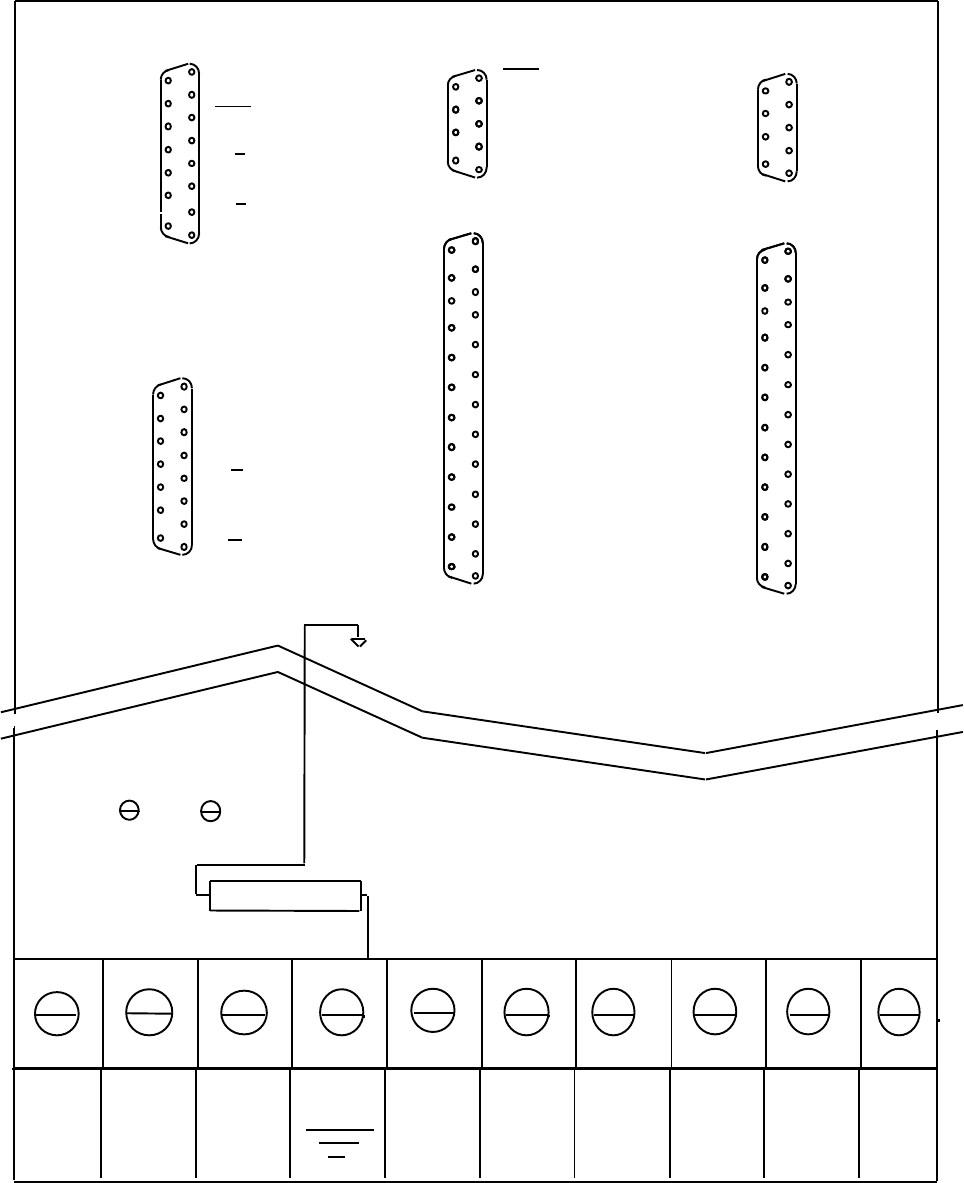
6.2 Wiring
Proper wiring, grounding and shielding techniques are important in obtaining
proper servo operation and performance. Incorrect wiring, grounding or
shielding can cause erratic servo performance or even a complete lack of
operation.
a) Keep motor wires as far as possible from the signal level wiring (feedback
signals, control signals, etc.).
b) If additional inductors (chokes) are required, keep the wires between the
amplifier and the chokes as short as possible.
c) Minimize lead lengths as much as is practical. Although the amplifier is
protected against long (inductive) supply wires it is recommended to keep
the leads as short as possible.
d) Use twisted and shielded wires for connecting all signals (command and
feedback). Avoid running these leads in close proximity to power leads or
other sources of EMI noise.
e) Use a 4 wires twisted and shielded cable for the motor connection.
f) Shield must be connected at one end only to avoid ground loops.
g) All grounded components should be tied together at a single point (star
connection). This point should then be tied with a single conductor to an
earth ground point.
h) After wiring is completed, carefully inspect all conditions to ensure
tightness, good solder joint etc.

65
DBP - Rev 6/93
6.3 Load inductance
The total load inductance must be sufficient to keep the current ripple
within the limits - 50% of the adjusted continuous current limit. The current
ripple (Ir) can be calculated by using the following equation:
0.5 x Vs
Ir = ---------- (A)
f x L
L - load inductance in mH.
Vs - Voltage of the DC supply in Volts.
f - Frequency in KHz.
If motor inductance does not exceed this value, 3 chokes should be added (to
each motor phase) summing together the required inductance
Lch = L - Lp
Lch - Choke inductance
Lp - Total inductance between two phases (in Y connection it is the sum of two
phases).
6.4 AC power supply
AC power supply can be at any voltage in the range defined within the
technical specifications. It must have the capability to deliver power to the
amplifier (including peak power), without significant voltage drops. Any
voltage below the minimum or above the maximum will disable the amplifier.
The recommended AC voltage are:
1.2 x VAC(min) < VAC < 0.9 x VAC(max)
Note - Single phase connection:
When using a single phase supply, voltage drop due to loading is expected.
The magnitude of the voltage drop depends on the load current, motor velocity,
stiffness of the power source and total bus capacitance. It is recommended not
to use single phase connection for output current higher than 20A.
For 3U size amplifiers it is recommended to add external capacitance as
follows:
For 135V units up to 1200µF
For 270V units up to 600µF
66
DBP - Rev 6/93
6.5 Wiring diagrams
6.5.1 Motor's windings
DBP
Motor
A
B
C
Heatsink / GND
MA
MB
MC
Chassis
Minimum acceptance
======================================================================
DBP
Motor
A
B
C
Heatsink / GND
MA
MB
MC
Chassis
Power wires twisted together
Acceptable for most applications
======================================================================
DBP
Motor
A
B
C
Heatsink / GND
MA
MB
MC
Chassis
Power wires twisted and shielded
Optimum wiring, minimum RFI
67
DBP - Rev 6/93
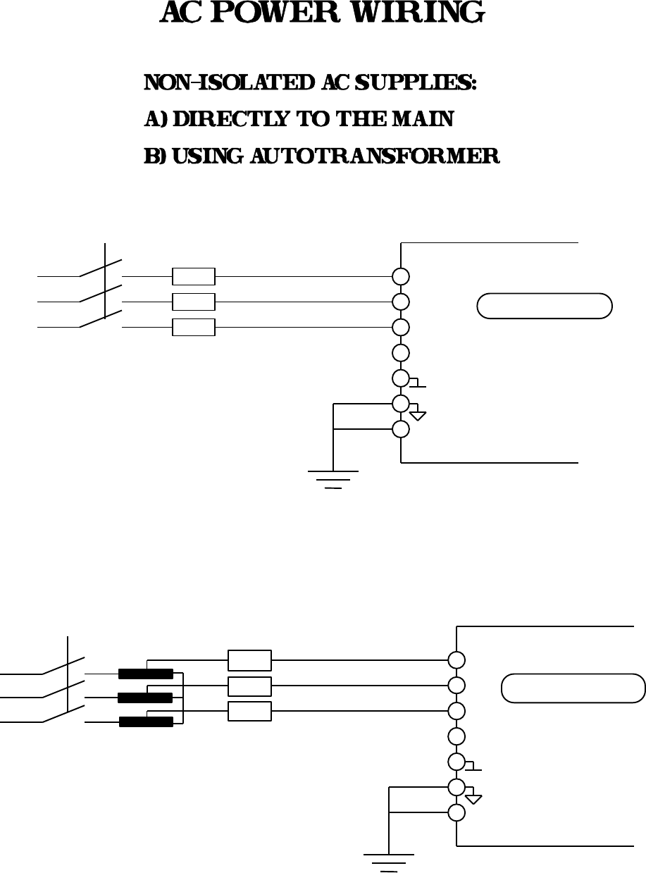
6.5.2 AC power wiring
AC
AC
AC
+Vs
DC power common
Control common
Heatsink
Fuse
Fuse
Fuse
A. Direct connection to the
three phase mains
B. External fuses are needed for 3U size only
DBP + O option
======================================================================
AC
AC
AC
+Vs
DC power common
Control common
Heatsink
Fuse
Fuse
Fuse
B. Using autotransformer with
Autotransformer
three phase mains
DBP + O option
A. External fuses are needed for 3U size only

68
DBP - Rev 6/93
Guide lines for connecting non-isolated AC supplies
Ground:
Control common
Motor chassis
Amplifier's heatsink
Do not ground:
Power common
(The power common is a hot point and any grounding will cause an input
rectifier failure).
Caution:
- If source of motor command is grounded, use amplifier's differential input.
Otherwise, a ground loop is created.
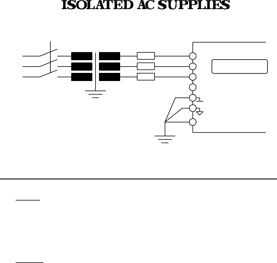
69
DBP - Rev 6/93
AC
AC
AC
+Vs
DC power common
Control common
Heatsink
Fuse
Fuse
Fuse
Isolating transformer
A. Extenal fuses are needed for 3U size only
DBP + I option
Guide lines for connecting an Isolated amplifier with an isolating power transformer
Ground:
DC power common
Control common
Motor chassis
Amplifier's heat sink.
Caution:
- If source of motor command is grounded, use amplifier's differential input.
Otherwise, a ground loop is created.
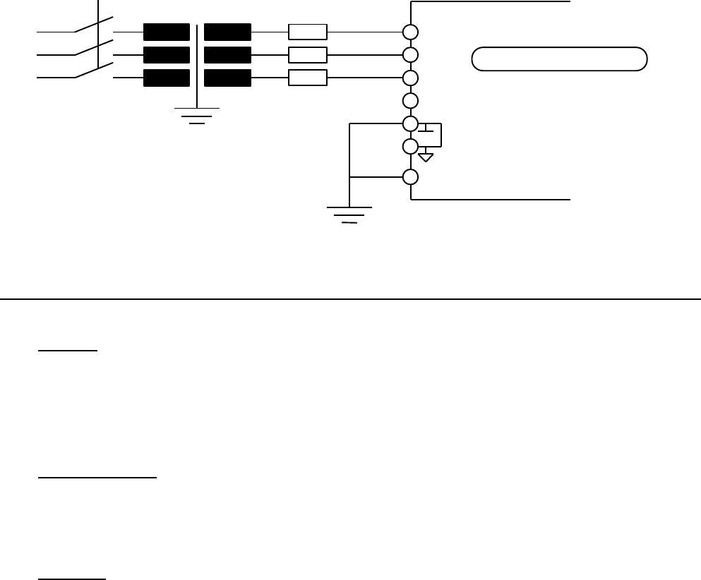
70
DBP - Rev 6/93
AC
AC
AC
+Vs
DC power common is internally
connected to control common
Heatsink
Fuse
Fuse
Fuse
Isolating transformer
NON-ISOLATED DBP
A. External fuses are needed for 3U size only
Guide lines for connecting a non isolated amplifier with an isolating power transformer
Ground:
DC power common
Motor chassis
Amplifier's heat sink
Do not ground:
Control common - It is internally connected to the power common. Grounding the
control common will create a ground loop.
Caution:
- If source of motor command is grounded, use amplifier's differential input.
Otherwise, a ground loop is created.
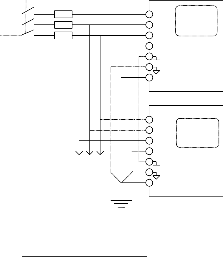
71
DBP - Rev 6/93
AC
AC
AC
+Vs
DC power common
Control common
Heatsink
Fuse
Fuse
Fuse
AC
AC
AC
+Vs
DC power common
Control common
Heatsink
To additional
DBPs
CONNECTING MORE THAN ONE DBP
DIRECT CONNECTION TO
THE THREE PHASE MAINS
NOTE: DC POWER TERMINALS ARE
CONNECTED IF SINGLE PHASE
IS USED OR IF SHUNT CURRENT
HAS TO BE INCREASED DBP
DBP
O option
O option
A. External fuses are needed
for 3U size only
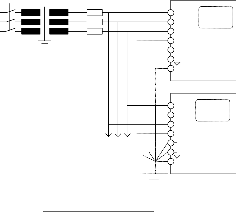
72
DBP - Rev 6/93
AC
AC
AC
+Vs
DC power common
Control common
Heatsink
Fuse
Fuse
Fuse
AC
AC
AC
+Vs
DC power common
Control common
Heatsink
To additional
DBPs
CONNECTING MORE THAN ONE DBP
ISOLATING
TRANSFORMER
NOTE: DC POWER TERMINALS ARE
CONNECTED IF SINGLE PHASE
IS USED OR IF SHUNT CURRENT
HAS TO BE INCREASED
DBP
DBP
A. External fuses are needed
for 3U size only
I option
I option
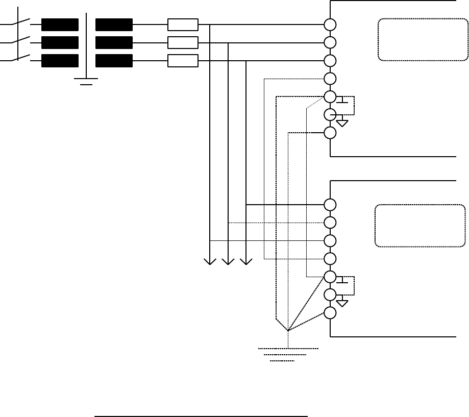
73
DBP - Rev 6/93
AC
AC
AC
+Vs
Heatsink
Fuse
Fuse
Fuse
AC
AC
AC
+Vs
Heatsink
To additional
DBPs
CONNECTING MORE THAN ONE DBP
ISOLATING
TRANSFORMER
ISOLATED DBP
ISOLATED DBP
NON
NON
NOTE: DC POWER TERMINALS ARE
CONNECTED IF SINGLE PHASE
IS USED OR IF SHUNT CURRENT
HAS TO BE INCREASED
DC POWER COMMON IS
INTERNALLY CONNECTED
TO CONTROL COMMON
DC POWER TERMINAL IS
INTERNALLY CONNECTED
TO CONTROL COMMON
A. External fuses are needed
for 3U size only
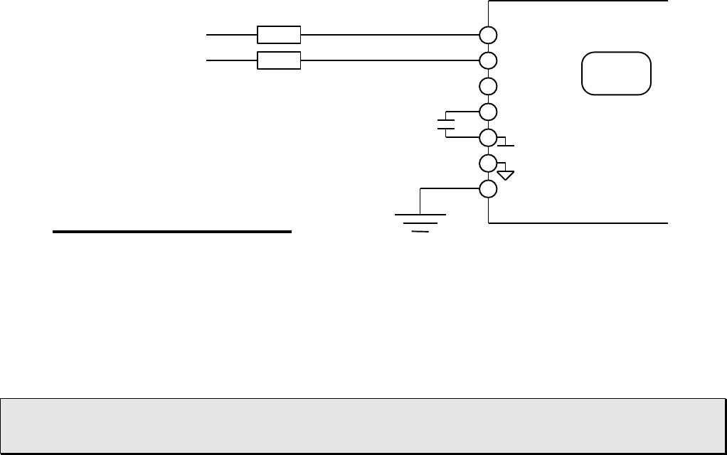
74
DBP - Rev 6/93
AC
AC
AC
+Vs
DC power common
Control common
Heatsink
Fuse
Fuse DBP
External
capacitance
SINGLE PHASE CONNECTION
See chapter 6.4 for details
All rules about supply connections described in the previous pages are also valid
for multi-IBP and/or single phase connection.
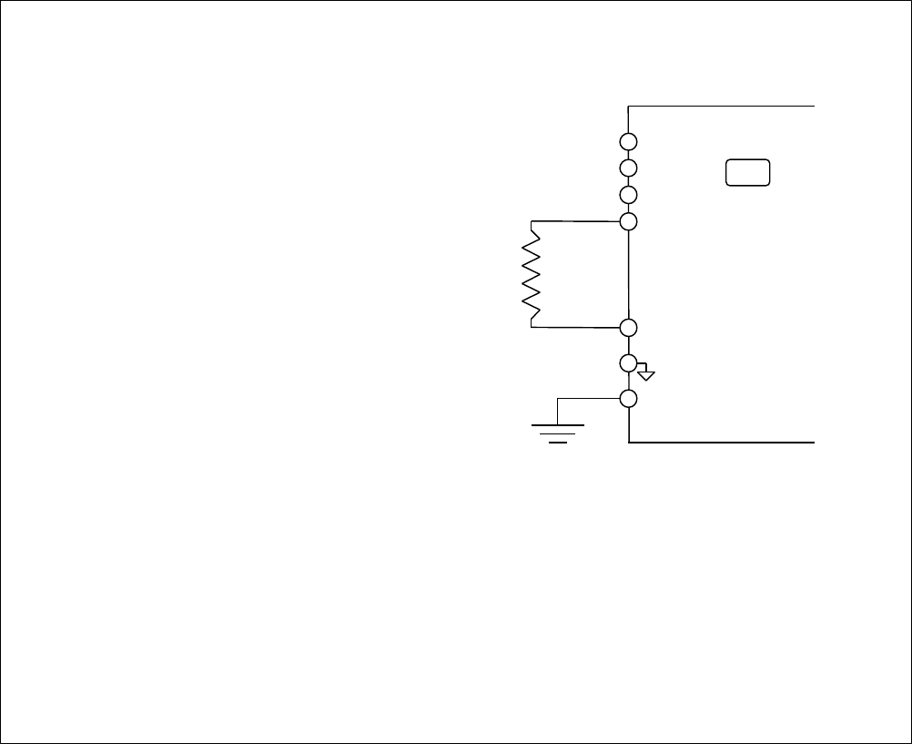
75
DBP - Rev 6/93
AC
AC
AC
+Vs
SO
Control common
Heatsink
DBP
CONNECTING THE EXTERNAL SHUNT RESISTOR
DOUBLE EUROCARD SIZE ONLY
For 135V types the standard value of
For 270V types the standard value of
Rex
Rex is 9.1ohm/225Watt
Rex is 33ohm/225Watt
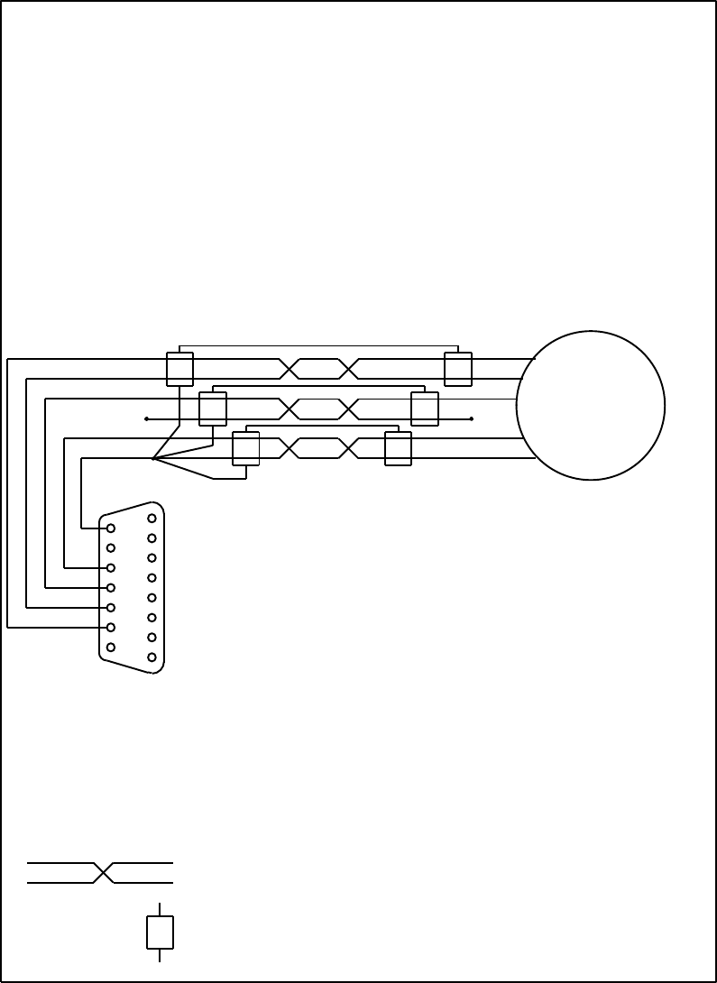
76
DBP - Rev 6/93
6.5.3 Hall sensors wiring
HALL A
HALL SENSORES
HALL SENSORES CONNECTION
J8
HALL B
HALL C
+15V
GND
4
5
6
7
8
11
12
13
14
15
1
2
3
9
10
REMARK:
TWISTED PAIR
SHIELDING
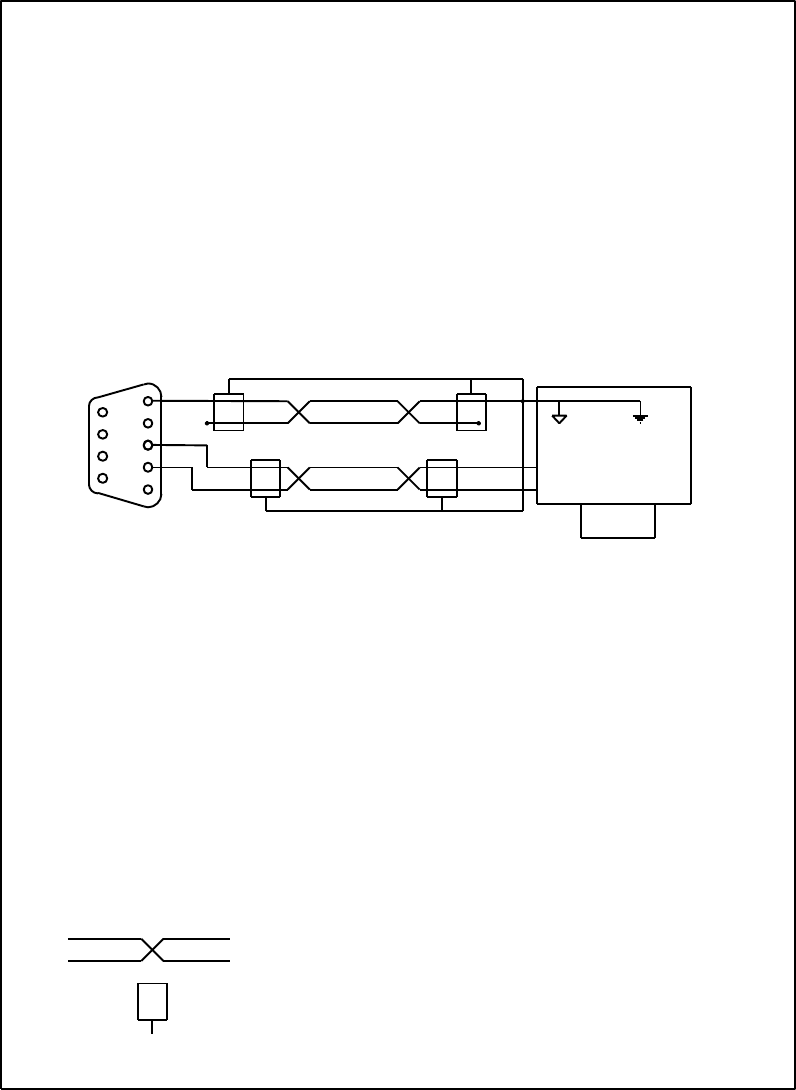
77
DBP - Rev 6/93
6.5.4 RS232 Communication wiring
RS232 COMMUNICATION
5
JC
6
9
8
7
1
2
3
4
R
TCOMPUTER
TXD
RXD
RST CTS
NOTE:
SHIELDING MUST BE CONNECTED AT COMPUTER END ONLY
SYMBOLS:
TWISTED PAIR
SHIELDING
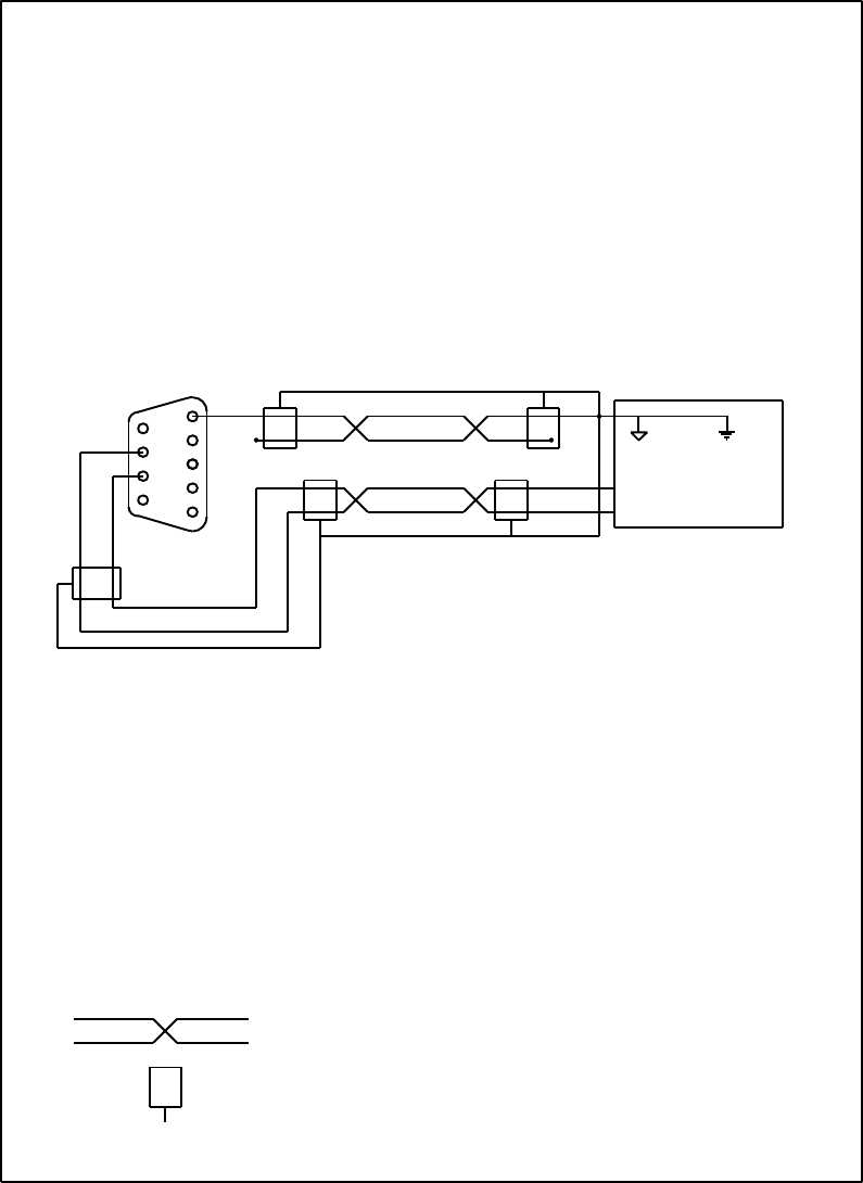
78
DBP - Rev 6/93
6.5.5 RS485 Communication wiring
RS 485 COMMUNICATION
95
JC
6
8
7
1
2
3
4
AMP. No 1
T/R+
T/R-
COMPUTER
NOTES:
1. SHIELDING MUST BE CONNECTED AT COMPUTER END ONLY
2. PIN No.1 TRANSMIT/RECEIVE CONTROL
3. PIN No.4 +5V
SYMBOLS:
TWISTED PAIR
SHIELDING
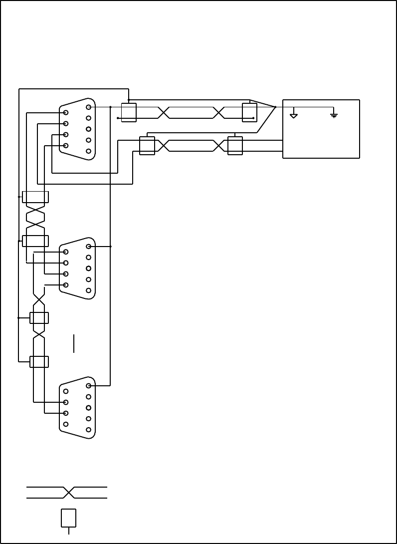
79
DBP - Rev 6/93
RS485 COMMUNICATION
9
83
4
5
JC
COMPUTER
T/R+
T/R-
6
7
1
2
AMP. No 1
9
83
4
5
JC
6
7
1
2
AMP. No 2
AMP. No 32
9
84
5
JC
NOTES:
2. PIN No.1 TRANSMIT/RECEIVE CONTROL
3. PIN No.4 +5V
1. SHIELDING MUST BE CONNECTED AT COMPUTER
END ONLY.
6
7
1
2
3
SYMBOLS:
TWISTED PAIR
SHIELDING
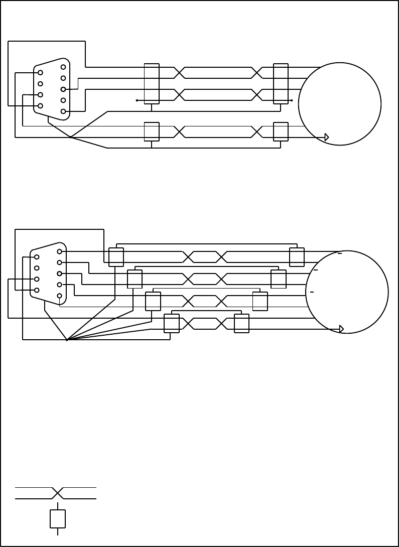
80
DBP - Rev 6/93
6.5.6 Main encoder wiring
ENCODER CONNECTION
J1
6
9
8
7
1
2
3
4
5
+V
ENCODER
B
A
I
DIFFERENTIAL ENCODER CONNECTION
J1
9
84
5
II
ENCODER
A
B
B
+V
A
1
2
3
6
7
NOTES:
1.THIS CONNECTION IS FOR AN ENCODER WITH +5V SUPPLY.
SYMBOLS:
COMMON. THE SHIELDING SHOULD BE CONNECTED EITHER
2.THE METAL FRAME OF J1 IS INTERNALLY CONNECTED TO THE DCB
FOR AN ENCODER OF +15V SUPPLY, USE J1 PIN 8 INSTEAD OF PIN 7.
TO J1 PIN 9 OR TO THE METAL FRAME OF J1.
TWISTED PAIR
SHIELDING
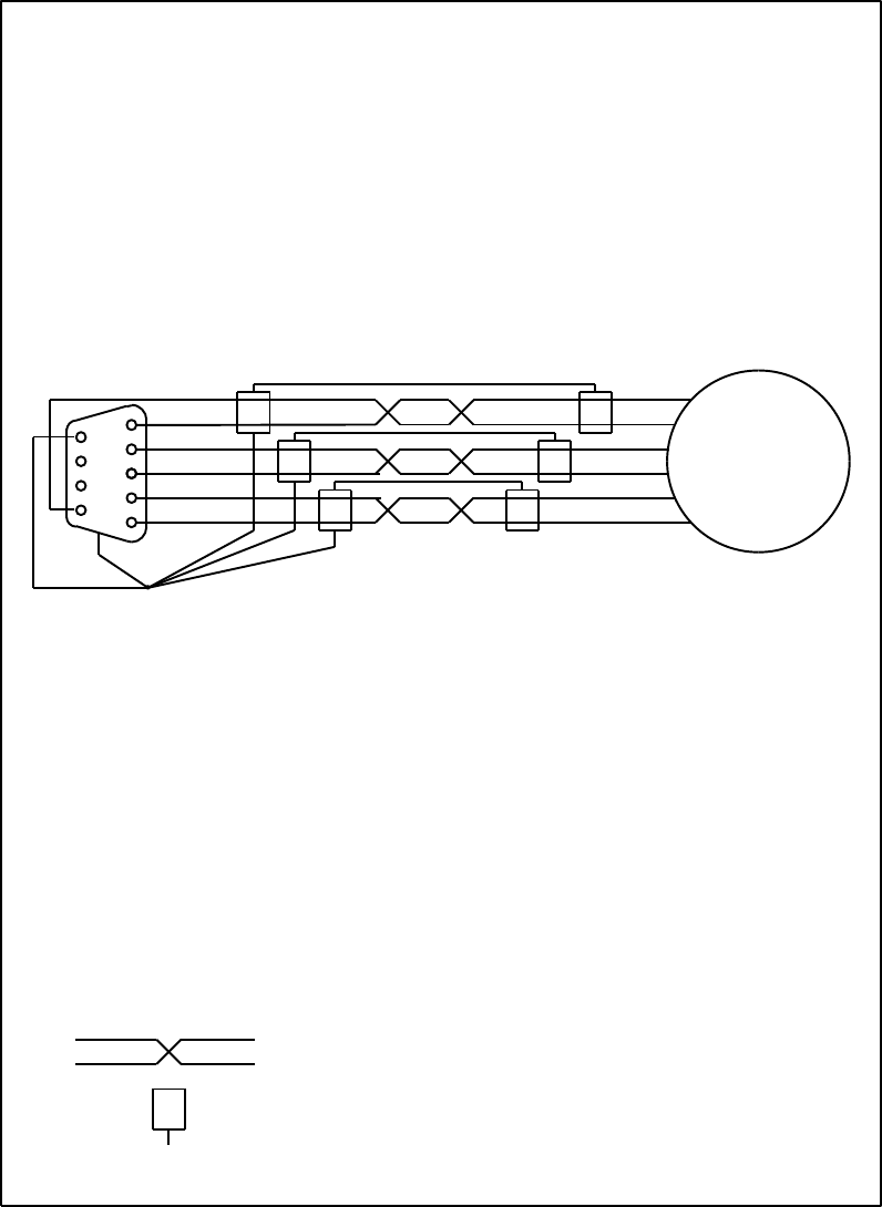
81
DBP - Rev 6/93
6.5.7 Resolver wiring
RESOLVER CONNECTION
RESOLVER
S3
S1
5
9
J2
6
8
7
1
2
3
4S4
S2
R2
R1
NOTES:
1. PIN No 7 = +15V
2. PIN No 8 = -15V
3. PIN 9 AND THE METAL FRAME OF J2 ARE INTENALLY CONNECTED
TO THE DCB COMMON. THE SHIELDINGS OF ALL THE PAIRS
SYMBOLS:
FRAME OF J2.
SHOULD BE CONNECTED EITHER TO J2 PIN 9 OR TO THE
TWISTED PAIR
SHIELDING
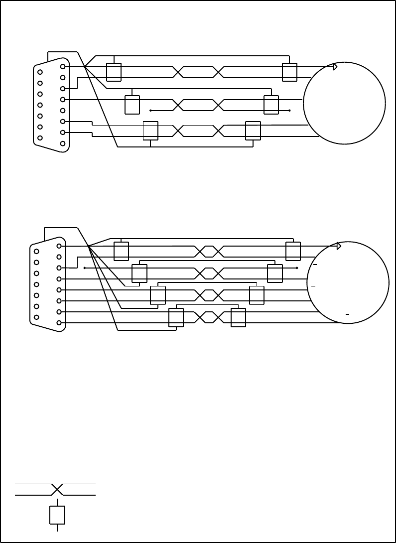
82
DBP - Rev 6/93
6.5.8 Auxiliary encoder wiring
AUXILIARY ENCODER CONNECTION
J6
10
11
12
13
14
15
2
3
4
5
6
7
8
+V
A
IENCODER
B
1
DIFFERENTIAL AUXILIARY
9
14
J6
6
7
8
ENCODER CONNECTION
+V
I
I
AA
BB
ENCODER
1
2
3
4
5
9
10
11
12
13
NOTES:
1.THIS CONNECTION IS FOR AN ENCODER WITH +5V SUPPLY.
SYMBOLS:
FOR AN ENCODER OF +15V SUPPLY, USE J6 PIN 7 INSTEAD OF PIN 6.
TO J6 PIN 8 OR TO THE METAL FRAME OF J6.
2.THE METAL FRAME OF J6 AND PIN 8 ARE INTERNALLY CONNECTED TO
THE DCB COMMON. THE SHIELDING SHOULD BE CONNECTED EITHER
TWISTED PAIR
SHIELDING
83
DBP - Rev 6/93
6.5.9 Pulse/Direction signals wiring
PULSE & DIRECTION INPUT CONNECTION
J6
10
11
12
13
14
15
2
3
4
5
6
7
8
CONTROLLER
DIRECTION
1
DIFFERENTIAL PULSE & DIRECTION
9
14
J6
6
7
8
INPUT CONNECTION
- PULSE
PULSE
DIRECTION
- DIRECTION
CONTROLLER
1
2
3
4
5
9
10
11
12
13
NOTES:
SYMBOLS:
TO J6 PIN 8 OR TO THE METAL FRAME OF J6.
1.THE METAL FRAME OF J6 AND PIN 8 ARE INTERNALLY CONNECTED TO
THE DCB COMMON. THE SHIELDING SHOULD BE CONNECTED EITHER
TWISTED PAIR
SHIELDING
PULSE

84
DBP - Rev 6/93
7. Start - Up Procedures
7.1 Common procedures for all amplifiers types
7.1.1 Commutation signals format
Select the position of DIP switch 1 on the upper board of the power stage
according to the commutation signal format the motor has.
DS1 positions: ON (down): 30°OFF (up): 60°
For all Resolver versions it should be 60 °.
7.1.2 CFM function
Select the position of DIP switch 2 on the upper board of the power stage
according to the motor's rated current. If it is less than 20% of the
amplifier's rated current select:
DS2 to ON (down)
Otherwise,
DS2 to OFF (up) - No CFM
7.1.3 Abort logic
Make sure that the Abort input is connected to a High (logic) voltage
source.

85
DBP - Rev 6/93
7.1.4 Setting the auxiliary position input format
This step is valid only for those applications that need to use the auxiliary
position input. You may skip this step if you do not use it.
When using an Optical encoder
Set DS 7 to OFF
When a the encoder has differential outputs:
Set DS 4 and 5 to OFF
Otherwise they should be ON.
When using Pulse and Direction signals
Set DS 7 to ON
7.1.5 Selecting the communication bus
Select the desired communication bus as follows:
For RS232: Set DS9 to OFF
For RS485: Set DS9 to ON
7.1.6 Preparing the automatic baud rate selection
The DCB baud rate will automatically match the host baud rate when DS1 is
set to ON.
Set DS1 to ON

86
DBP - Rev 6/93
7.2 Setting the main optical encoder format
When a differential encoder is used:
Set DS 2,3,6 to OFF
Otherwise they should be ON.
7.3 Setting the R/D circuit
Set DS 2,3,6 to ON
The Resolver interface circuit consists of three basic blocks:
R/D converter
The R/D conversion is done by a variable resolution, monolithic converter
type 2S82 of Analog Devices. It accepts two signals from the Resolver (sine and
cos.) and converts them into binary position data bits. The resolution of the
position bits is user selectable 10, 12 ,14 and 16 (only for standard encoder
resolution). In addition, the R/D creates a signal that is proportional to the
Resolver velocity. This signal is being used as a velocity feedback.
EPROM
The EPROM creates "Hall" signals by mapping the position data bits accepted
from R/D into suitable Hall signals to operate a specific brushless motor. In
addition, the encoder index (marker) signal is also produced from the EPROM.
The EPROM is designated as follows:
2 4 X S STD
Resolver's poles number
Ratio of motor/resolver
poles numbers
Encoder resolution
Commutation address
R/D resolution
X=User selectable, 0=10 bits
2=12 bits, 4=14 bits, 6=16 bits
In the S (standard) version zero crossing of phases B C occurs at position
address "0" of the Resolver.

87
DBP - Rev 6/93
Oscillator
Creates sinusoidal waveform signal to excite the primary of the Resolver.
Oscillator Frequency/Amplitude Selection (R228,R233)
The frequency (fr) and amplitude (Vr) needed to excite the Resolver are
taken from the Resolver data sheet.
Selecting the frequency:
R228 = 110/fr (Kohm)
0.1KHz < fr (KHz) < 20KHz
Selecting the amplitude:
Pay attention that the RMS amplitude does not exceed 7Vrms or that the peak-
to-peak (ptp) value is within the range of 2V < Vrptp < 20V. For Vr in
peak-to-peak value:
R233 = 6/(Vr - 2) (Kohm)
For Vr in RMS value:
R233 = 6/(2.82Vr - 2) (Kohm)
Reference Voltage level to R/D (R192)
In order to adjust the reference voltage input level to 2Vrms, select R192
as follows:
R192 = 50 x (Vrrms - 2) (Kohm)
For Vrrms <2V, install R192=100 ohm.

88
DBP - Rev 6/93
Signal input level (R193,R194)
The R/D inputs (Vinrms) are adjusted to the sin/cos. Resolver outputs by:
Resolver output = Vinrms = Vrrms x Transformation ratio
R193 = R194 = Vinrms - 2 - Rstator (Kohm)
(Rstator in Kohm).
When Vinrms<2V, install R193=R194=100 ohm.
The standard R/D converter will not operate for Vin rms<1.8V. Consult factory
for OEM applications.
Velocity Signal
The tracking converter technique generates an internal signal at the output of
the integrator that is proportional to the rate of change of the input angle.
This dc analog output (velocity signal) is buffered and represented at terminal
H/R-12b,E-J3/23. Max output voltage is +8V.
This velocity signal can be internally connected to the summing junction of
the error amplifier by inserting R7 - see Appendix B for more details. However,
the standard procedure does not require closing the velocity loop.
Select maximum actual velocity of the application and calculate the maximum
tracking rate T of the Resolver as follows:
T = rpm x Q / 120
T unit is rps: Resolver electrical revolution per second
Q - number of poles of Resolver ;
rpm - mechanical revolution per minute.
Selecting the Resolution
The resolution can be selected to be 10,12,14 or 16 bits by use of DIP
switches 13 and 14. When selecting the resolution the rps limits should not be
exceeded:
89
DBP - Rev 6/93
10 bit = 1040 rps
12 bit = 260 rps
14 bit = 65 rps
16 bit = 16.5rps
Resolution DS13 DS14
10 ON ON
12 ON OFF
14 OFF ON
16 OFF OFF
Note:
- Each resolution change must be followed by new components selection
procedure.
- When changing resolution under dynamic conditions, a period of uncertainty
will exist before position and velocity data is valid.
Encoder resolution
In the STD mode (DS12 OFF), the encoder signals A,B are created by the EPLD
and can have only the following basic resolutions (for 2 pole Resolver):
256 for 10 bits
1024 for 12 bits
4096 for 14 and 16 bits
When the Resolver is more than 2 poles, the resolution for one shaft
rotation will be:
Er = QxS / 8
Q = number of Resolver poles ;
S = resolution of converter (2 10,212,or 214)
When different encoder resolution is needed the encoder signals are
generated by the EPROM and the R/D resolution is no longer user selectable.
This option requires
- DS12 at ON
- Special EPROM which is programmed for this resolution.

90
DBP - Rev 6/93
HF Filter (R195, R196, C61, C62)
The function of the HF filter is to reduce the amount of noise present on
the signal inputs to the 2S82, reaching the Phase Sensitive Detector and
affecting the outputs. Values should be chosen so that
15Kohm < R195=R196 < 30Kohm
160x103
C61 = C62 = ------------ (pF)
R195 x fr
fr = Reference frequency in KHz
R195 in Kohm
This filter gives an attenuation of 3 times at the input to the phase
sensitive detector.
AC Coupling of Reference Input (C60)
Select C60 so that there is no significant phase shift at the reference
frequency. That is,
106 100 x R192
C60 = -------------- (pF) Rx = ------------ (Kohm)
fr(KHz) x Rx 100 + R192
R192 in Kohm
If Rx yields less than 50K, install a value of Rx=50K in the C60 equation.
Maximum Tracking Rate (R201)
The VCO input resistor R201 sets the maximum tracking rate of the converter
and hence the velocity scaling as at the maximum tracking rate, the velocity
output will be 8V.
Decide on your required maximum tracking rate, "T" , in revolutions per
second. Note that "T" must not exceed the specified maximum tracking rate or
1/16 of the reference frequency.

91
DBP - Rev 6/93
R201 = 5.92 x 10⁷ / T x p (Kohm)
where p = bit per rev
= 1,024 for 10 bits resolution
= 4,096 for 12 bits
= 16,384 for 14 bits
= 65,536 for 16 bits
Closed Loop Bandwidth Selection (C67, C68, R200)
a. Choose the Closed Loop 3dB Bandwidth (f bw) required ensuring that
fref > 10 x fbw
Recommended bandwidth values:
250Hz for 3KHz
300Hz for 5KHz
500Hz for 10KHz
b. Select C67 so that
2.5x10⁹
C67 = ------------- (pF)
R201 x fbw2
with R201 in Kohm and fbw in Hz as selected above.
c. C68 is given by
C68 = 40 x C67 (pF)

92
DBP - Rev 6/93
d. R200 is given by
127 x 107
R200 = ------------- (Kohm)
fbw x C68
fbw in Hz, C68 in pF
R200 value should be at least three times R197.
Gain Scaling Resistor (R197)
R197 should be installed according the following table:
536Kohm for 10 bits resolution
130Kohm for 12 bits
33Kohm for 14 bits
8.2Kohm for 16 bits
93
DBP - Rev 6/93
8. Applying power - Adjustments
Important remarks:
A. If all the previous steps were accomplished you may now disconnect the motor
leads, turn the power on and continue with the following adjustments.
Step 1 - Applying Power
Apply power and check for LED Vs of the DCB that should be "ON", indicating
that the system supplies are present. The display should read: "F-OK". If you
get another message, refer to the following table to find the cause of the
problem. Turn the power off, clear the cause of the problem and re-power the
unit.
Event Display Display
after
Recurring
DIP switch 1 - ON BAUD OK
Load is under cont. current limit CLIM C-OK
Battery Low BATT B-OK
Abort condition (hardware only) ABRT A-OK
Amplifier's power stage disabled *AMPD H-OK
-15V out of limits -15V F-OK
Under or Over Voltage VOLT F-OK
+15V out of limits +15V F-OK
Over Temperature TEMP F-OK
Commutation problem CMMT F-OK
Short condition at the power outputs SHRT F-OK
* The AMPD message appears in two cases:
1. When MO (Motor Off) command is given.
2. Position error exceeds the allowed value.

94
DBP - Rev 6/93
Step 2 - Establishing the communication
Press CR (carriage return) in the host several times until the DCB sends the
message "Communication OK".
If you want to "lock" the baud rate in the DCB:
- Turn off the power and remove the amplifier from the rack if it is a rack
version.
- Set DS1-OFF.
Now the baud rate you selected is stored in the SRAM.
It is possible to change DS1 at any time. However, the DCB will notice the change
only upon power on or hardware reset.
Step 3 - Checking the feedback elements
- Turn on the power.
- Rotate the motor shaft manually and interrogate the position with the
instruction:
TP (CR)
The controller response should vary as the motor is turned. If this does not
occur, check the feedback signals.
- When using the auxiliary encoder input, rotate the auxiliary encoder and
interrogate the position with the instruction: PY.
The controller response should vary as the encoder is turned. If this does
not occur, check the feedback signals. The DCB is counting quadrature pulses.
This means that for encoders or resolvers the answer for a TP command will be 4
times the number of basic encoder pulses and for Pulse/Direction mode it will
be twice the number of pulses.
Step 4 - Adjusting the current limits
Defining the amplifier type
- Define the maximum current of the amplifier by the instruction:
MCn
n - rated peak current of the amplifier in A as given in the table of chapter
3.
For example: n is 48 for DBPF-24/270

95
DBP - Rev 6/93
Current limit adjustments
- Define the continuous current limit by the instruction:
CLn.m (n.m - current in A)
- Define the peak current limit by the instruction:
PLn.m (n.m - current in A)
- Define the maximum peak current duration by the instruction:
PDn.m (n.m - seconds)
Step 5 - Latch mode of the protective functions
All the protective functions activate internal inhibit. There are two modes
of resetting the amplifier after the cause of the inhibit disappears:
Self Restart: (LM0)
The amplifier is inhibited only for the period that the inhibit cause is
present.
Latch (LM1)
Each failure latches the Inhibit and the failure message on the display. For
restart (after clearing the failure source), reset has to be performed by
applying logic 0 at the reset input (H/R-17a,E-J3/21), or by turning the power
off and on.
For safety reason it is recommended to use the amplifier in the LATCH MODE - LM1
Step 6 - Connecting the Motor
- Turn off the power.
- Connect the leads of the motor.
- Turn on the power.
For proper operation, the system must have negative feedback. If the motor
remains in the same position and returns to the same position when you turn the
motor shaft and let go, then the position feedback is negative as required. If
the motor runs away you have positive feedback. To correct the feedback, just
reverse the encoder leads.

96
DBP - Rev 6/93
9. Tables and Summaries
9.1 Display diagnostics
Each amplifier's fault is stored immediately in the DCB RAM. In addition to
that, a Failure Message is displayed. Following are all the valid Display
Messages:
Event Display Display
after
Recurring
DIP switch 1 - ON BAUD OK
Load is under cont. current limit CLIM C-OK
Battery Low BATT B-OK
Abort condition (hardware only) ABRT A-OK
Amplifier's power stage disabled *AMPD H-OK
-15V out of limits -15V F-OK
Under or Over Voltage VOLT F-OK
+15V out of limits +15V F-OK
Over Temperature TEMP F-OK
Commutation problem (for brushless drives
only)
CMMT F-OK
Short condition at the power outputs SHRT F-OK
* The AMPD message appears in two cases:
1. When MO (Motor Off) command is given.
2. Position error exceeds the allowed value.
97
DBP - Rev 6/93
9.2 Summary of DIP switches
Power stage board
(2 poles DIP switch)
DIP switch OFF (UP) ON (DOWN)
DS1 60° commutation signals format 30° commutation signals format
DS2 No CFM Activate CFM
Control stage board
(9 poles DIP switch)
DIP switch ON OFF
DS1 Auto-selection of Baud rate Latch last value
DS2 Non-differential channel A Diff. input of channel A
DS3 Non-differential channel B Diff. input of channel B
DS4 Non-differential channel Ay Diff. input of channel Ay
DS5 Non-differential channel By Diff. input of channel By
DS6 Non-differential index Diff. index
DS7 Pulse/Direction format Encoder channels format
DS8 N/C
DS9 RS485 RS232
4 poles DIP switch (for Resolver)
Switch OFF ON
DS11 Tacho signal disconnected Tacho signal connected to error
amplifier.
DS12 Standard encoder resolution Non-standard encoder resolution
DS13 14 bit resolution (DS14-ON)
16 bit resolution (DS14-OFF)
10 bit resolution (DS14-ON)
12 bit resolution (DS14-OFF)
DS14 12 bit resolution (DS13-ON)
16 bit resolution (DS13-OFF)
10 bit resolution (DS13-ON)
14 bit resolution (DS13-OFF)

98
DBP - Rev 6/93
Appendix A - Current loop response
In most applications it is not necessary to adjust the current loop to
achieve the optimum response. When there are extreme electrical parameters in
the armature circuit (inductance and resistance) the standard components values
of 0.01µF for C1 and 100Kohm for R4 may not yield with the optimum response.
The current loop should be optimized as follows:
- Insert R7 (1K) to connect the tacho input to the error amplifier. The
amplifier must not be configured into velocity mode. If the resolver option
is used, make sure that DS11 is OFF.
- Apply power to the amplifier and send the command BA.
- Provide the tacho input H/R-12b,E-J3/23 with a bi-directional square wave
current command (100-200Hz, +2.0V waveform is often employed).
- Monitor the load current either by a current probe or by the current monitor.
If the current response is not critically damped, use the following
procedure:
- Short circuit C1 with a short jumper wire.
- Replace R4 with a decade resistance box. Initially set the box resistance at
10Kohm.
- Apply the square wave test signal to the amplifier input.
- Apply power, and while monitoring the load current, gradually increase the
value of the box resistance until optimum response as depicted in Fig A-1 is
achieved.
- Substitute the closest standard value discrete resistor for R4 and remove the
decade resistance box.
- Remove the shorting jumper across C1, and again check the response using the
square wave test signal.
- If the previous step does not yield satisfactory results, if unacceptable
overshooting has been noted, substitute a larger value than 0.01 µF; or, if
the response is overdamped, substitute a smaller value than 0.01 µF.
Repetition of this procedure should yield an optimum choice for C1.
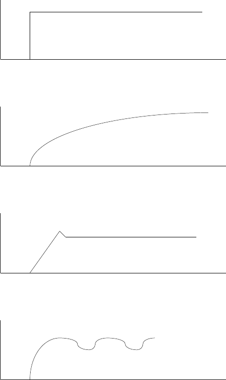
99
DBP - Rev 6/93
Reference input signal
C1 too large / R4 too small
Critically damped
C1 too small / R4 too large
Fig. A-1
Typical current response waveforms

100
DBP - Rev 6/93
Appendix B - Adding a velocity feedback
THIS PAGE IS BLANK

101
DBP - Rev 6/93
Appendix C - Differential amplifier connection
The differential amplifier is provided for your optional use. It can be used
for buffering, inverting or elimination of common mode signals.
The differential amplifier inputs are available at terminals H/R-9b,E-J3/1,
H/R-10b,E-J3/2. Terminal H/R-10b,E-J3/2 is the inverting input, terminal H/R-
9b,E-J3/1 is the non-inverting input. The output is on terminal H/R-11b,E-J3/3.
The differential amplifier can be internally connected to the summing junction
by inserting R800.
The differential amplifier may be used as a buffer or as an eliminator of
common mode signals. For a non-inverting buffer amplifier, connect the positive
signal lead to terminal H/R-9b,E-J3/1 and the negative signal lead to terminal
H/R-10b,E-J3/2, and connect terminal H/R-10b,E-J3/2 to the circuit common. For
an inverting buffer amplifier, connect the positive signal lead to terminal
H/R-10b,E-J3/2, the negative signal lead to terminal H/R-9b,E-J3/1, and connect
terminal H/R-9b,E-J3/1 to the circuit common. The output of the differential
amplifier is given by:
10xV1 10 10xV 2
Vo = ----------- x ( 1 + --- ) - -------
10 + R3 R2 R2
V1 - Input voltage of terminal H/R-9b,E-J3/1.
V2 - Input voltage of terminal H/R-10b,E-J3/2.
V1max < 10 + R3; V2max < 100/R2
See schematic in chapter 4.

102
DBP - Rev 6/93
DIMENSIONAL DRAWINGS
IN THE FOLLOWING DRAWINGS ALL THE DIMENSIONS ARE IN MILLIMETERS.
PANEL (H), DBP1................................ ................... 104
PANEL (H), DBP2................................ ................... 107
PANEL (H), DBP3................................ ................... 110
PANEL (H), DBP4................................ ................... 113
PANEL (H), DBP6................................ ................... 116
RACK 3U/13T................................ ....................... 119
RACK 3U/20T................................ ....................... 122
RACK 6U/14T................................ ....................... 125
RACK 6U/21T................................ ....................... 128
ENCD - 3U/................................... ..................... 130
ENCD - 6U/................................... ..................... 131
EXTERNAL SHUNT RESISTOR ................................ ...........132
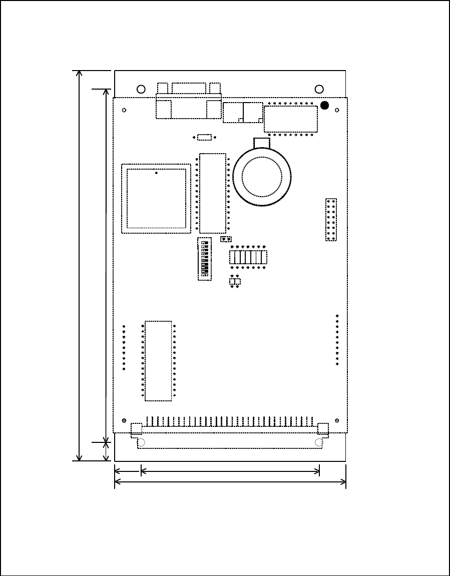
103
DBP - Rev 6/93
PANEL (H), DBP1
187 169
9
12.5 110
85
DBP1 - TOP VIEW
BATTERY
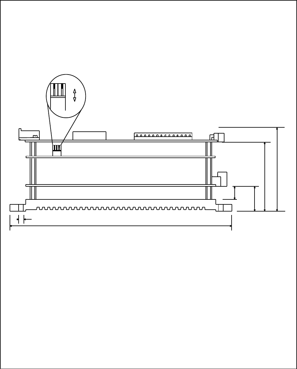
104
DBP - Rev 6/93
18.6
52.5
9.6
4.0 187
DBP1 - SIDE VIEW 1
1 2 ON
OFF
66
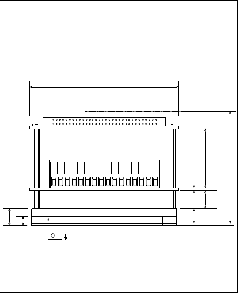
105
DBP - Rev 6/93
111.76
32
66
32.3
9
8
1.6
4
5
DBP1 - SIDE VIEW 2
6 7 8 910 11
3 4 51 21213 14 1516
b
a
1
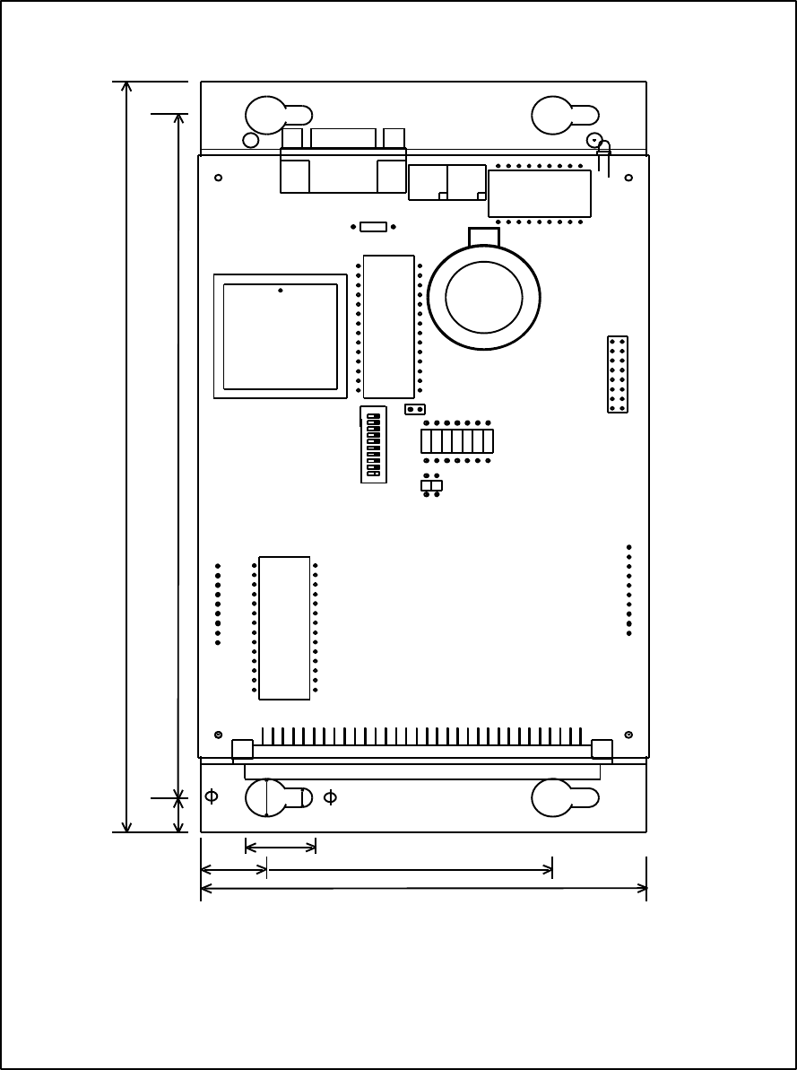
106
DBP - Rev 6/93
PANEL (H), DBP2
200 182
5
10
16
9
17
109
70
DBP2 - TOP VIEW
BATTERY
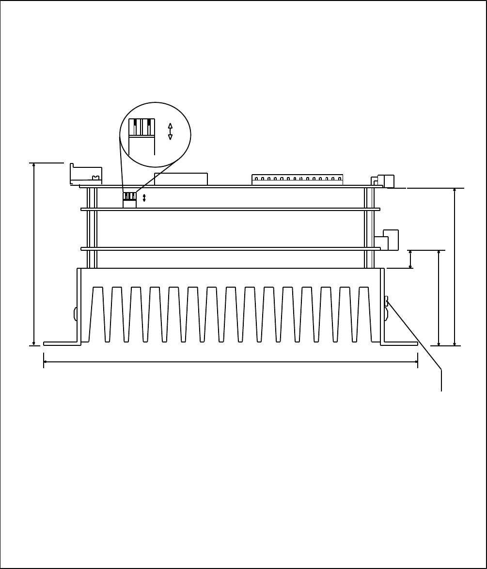
107
DBP - Rev 6/93
ON
OFF
1 2
85.5
9.6
51.2
GROUNDING
SCREW M4
200
DBP2 - SIDE VIEW 1
ON
OFF
1 2
102
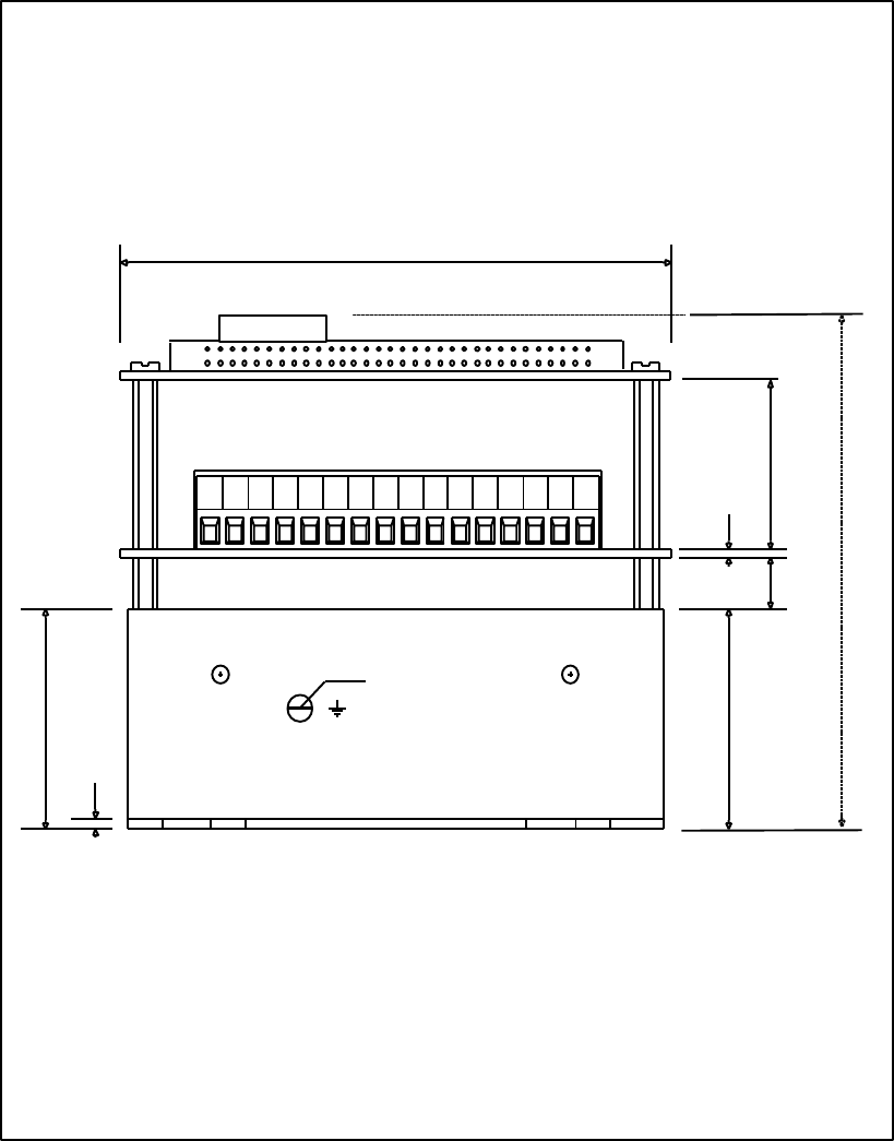
108
DBP - Rev 6/93
111.76
1 2 3 4 5 6 7 8 9 10 11
32.3
1.6
9.64
42
M4
40
2
DBP2 - SIDE VIEW 2
102
12 13 14 15 16
1
32
b
a
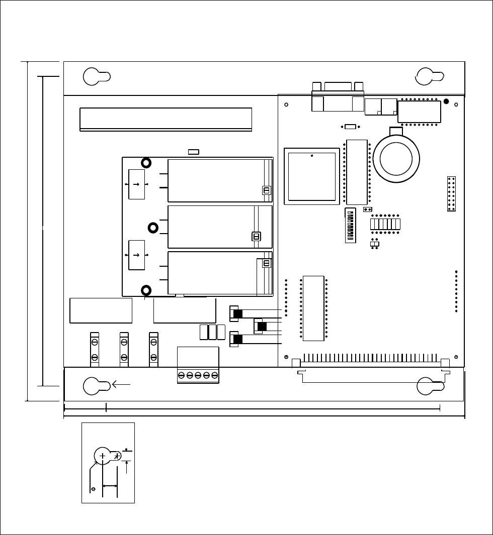
109
DBP - Rev 6/93
PANEL (H), DBP3
200 182
205
245
25
DBP3 - TOP VIEW
DETAIL A
10
10
DETAIL A.
5
SEE
BATTERY
JL
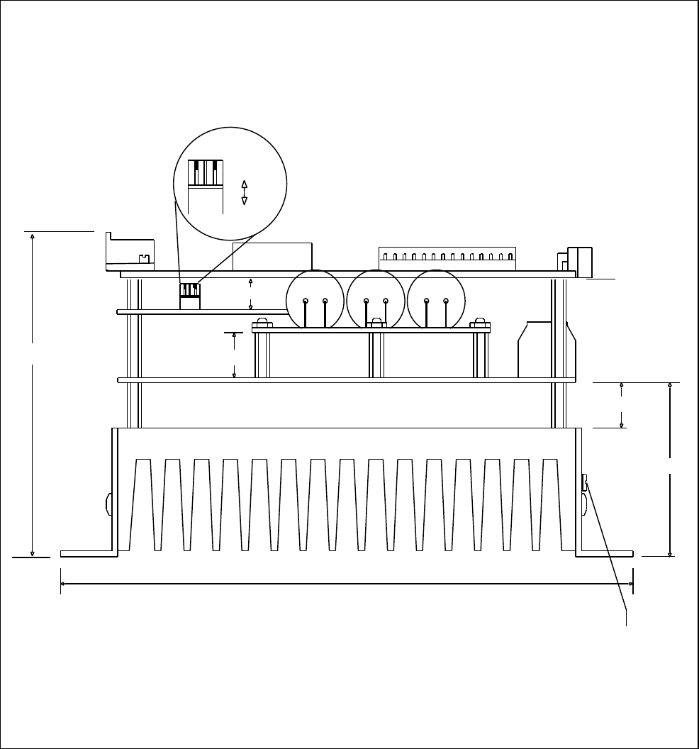
110
DBP - Rev 6/93
9.64
1 2
14.64
14.64
56.64
GROUNDING
200
SCREW M4
102
DBP3 - SIDE VIEW 1
ON
OFF
21
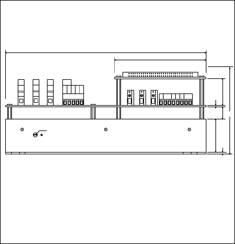
111
DBP - Rev 6/93
245.11
MA
1
MC
3
+-HA HB HC
FAN
111.76
AC AC AC
NC P.C NC SO NC +VS
32.3
1.6
40
2
14.6
M4
MB
2
105
DBP3 - SIDE VIEW 2
b
a
1
32
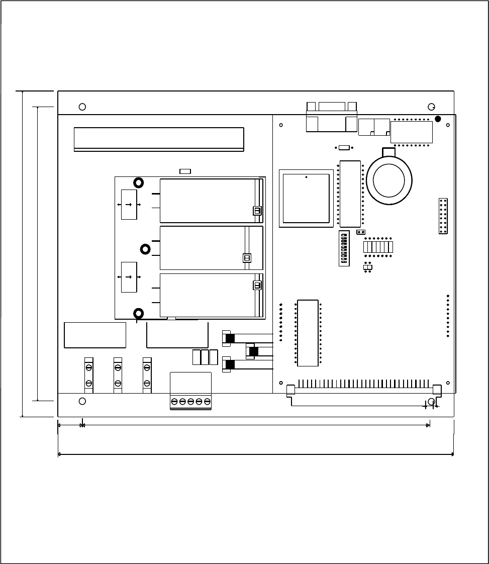
112
DBP - Rev 6/93
PANEL (H), DBP4
187 173.5
215
15
245
4
DBP4 - TOP VIEW
BATTERY
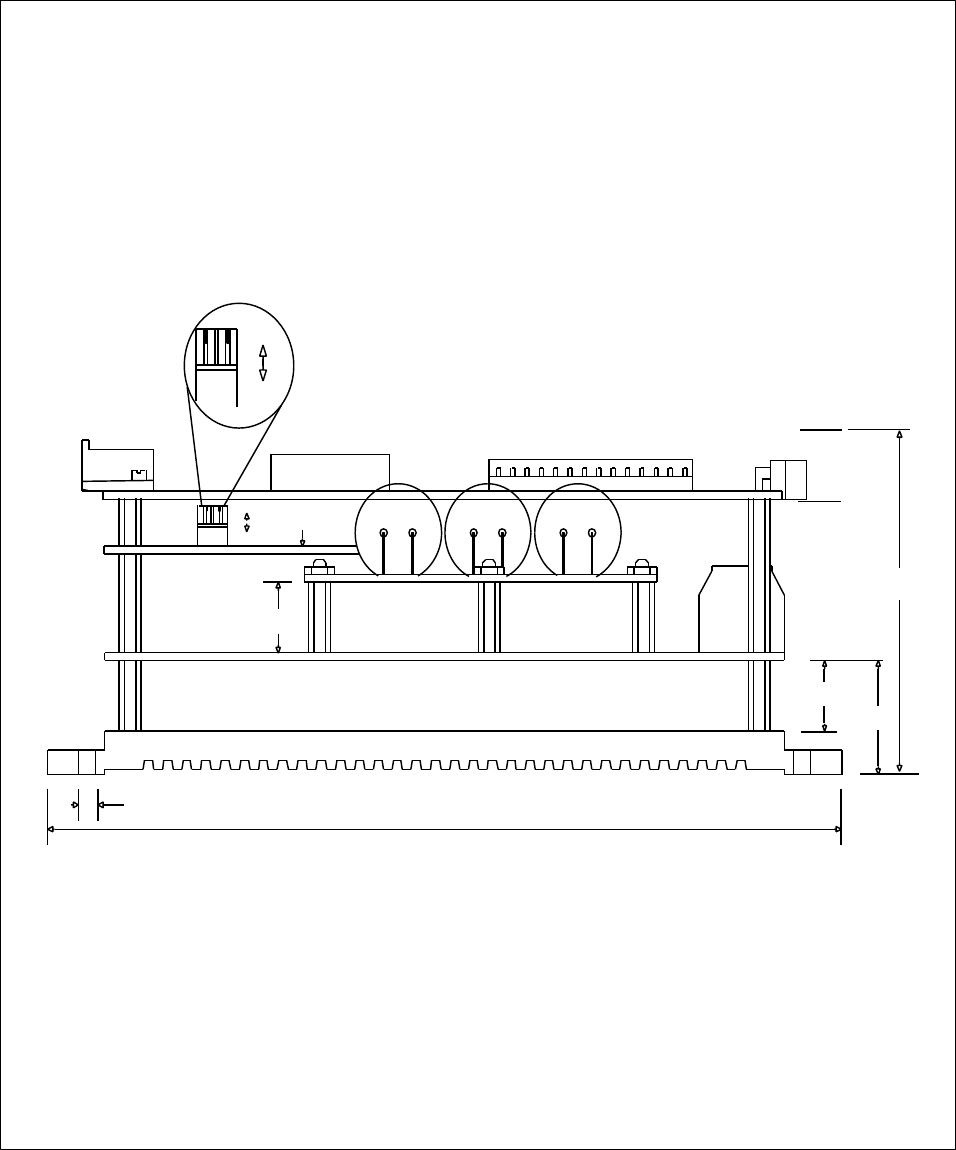
113
DBP - Rev 6/93
12
14.64
9.64
23.64
4.0
187
72.54
14.64
DBP4 - SIDE VIEW 1
SIDE VIEW
1 2 ON
OFF
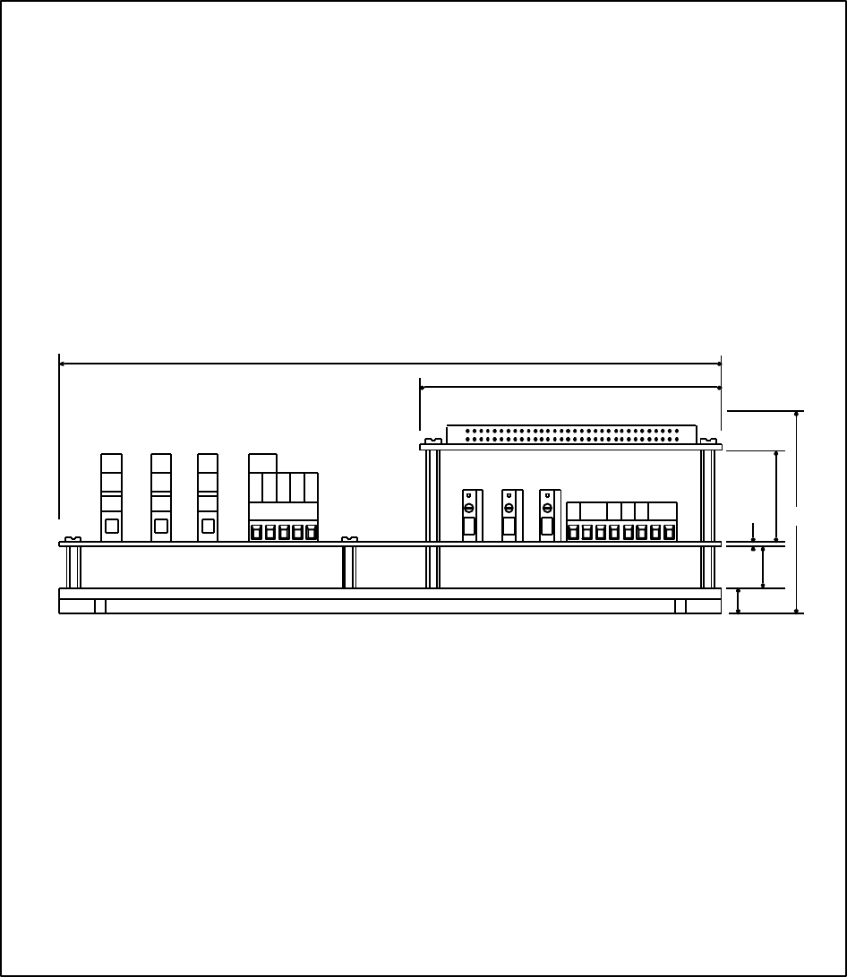
114
DBP - Rev 6/93
245.11
MA
1
MC
3
+-HA HB HC
FAN
111.76
AC AC AC
NC P.C NCSO NC +VS
32.3
1.6
14.64
MB
2
72.54
9
DBP4 - SIDE VIEW 2
b
a
1
32
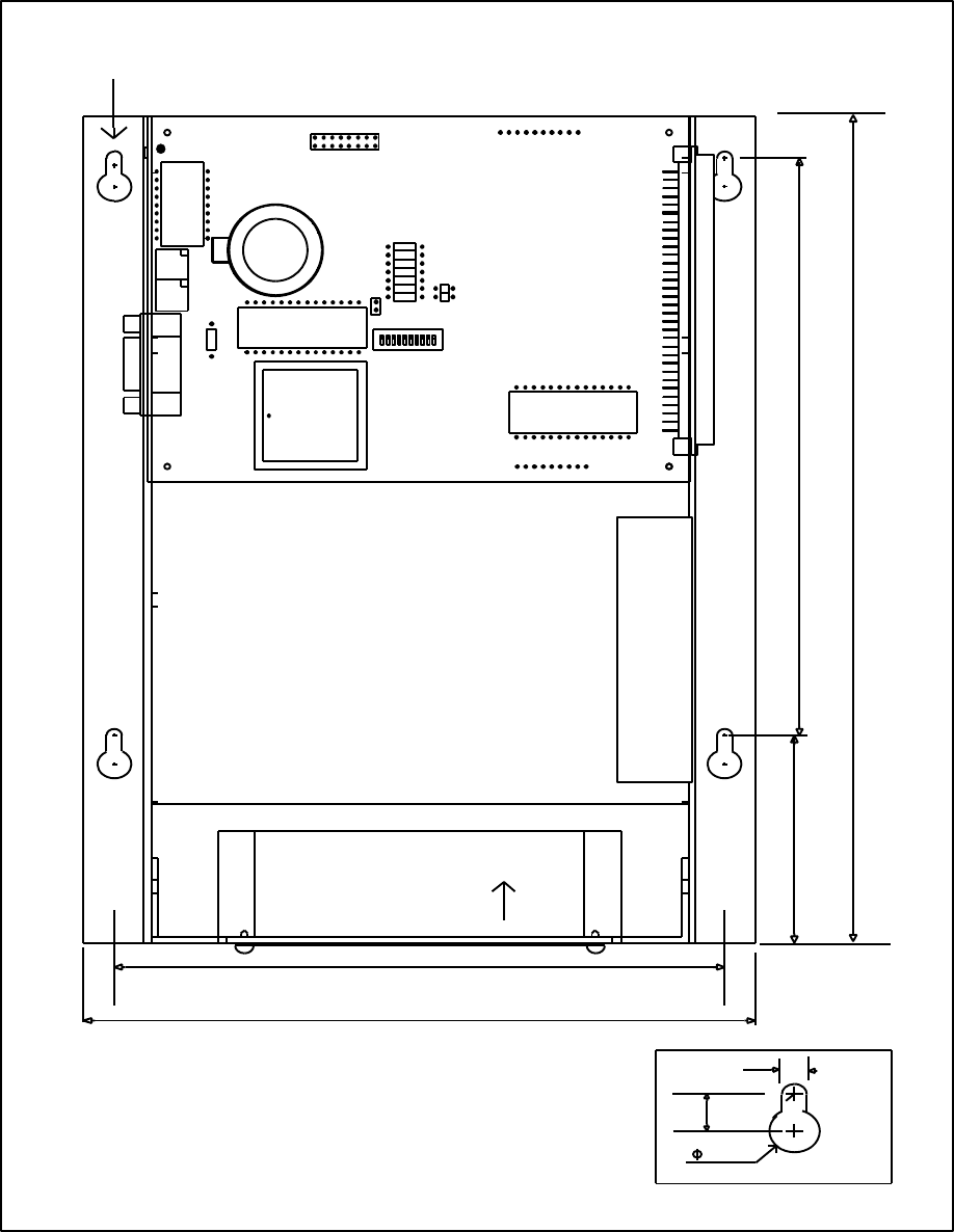
115
DBP - Rev 6/93
PANEL (H), DBP6
DBP6 - TOP VIEW
SEE DETAIL A
294205
POWER
CONN.
74
182
AIR FLOW
FAN
200
10
10
DETAIL A.
5
BATTERY
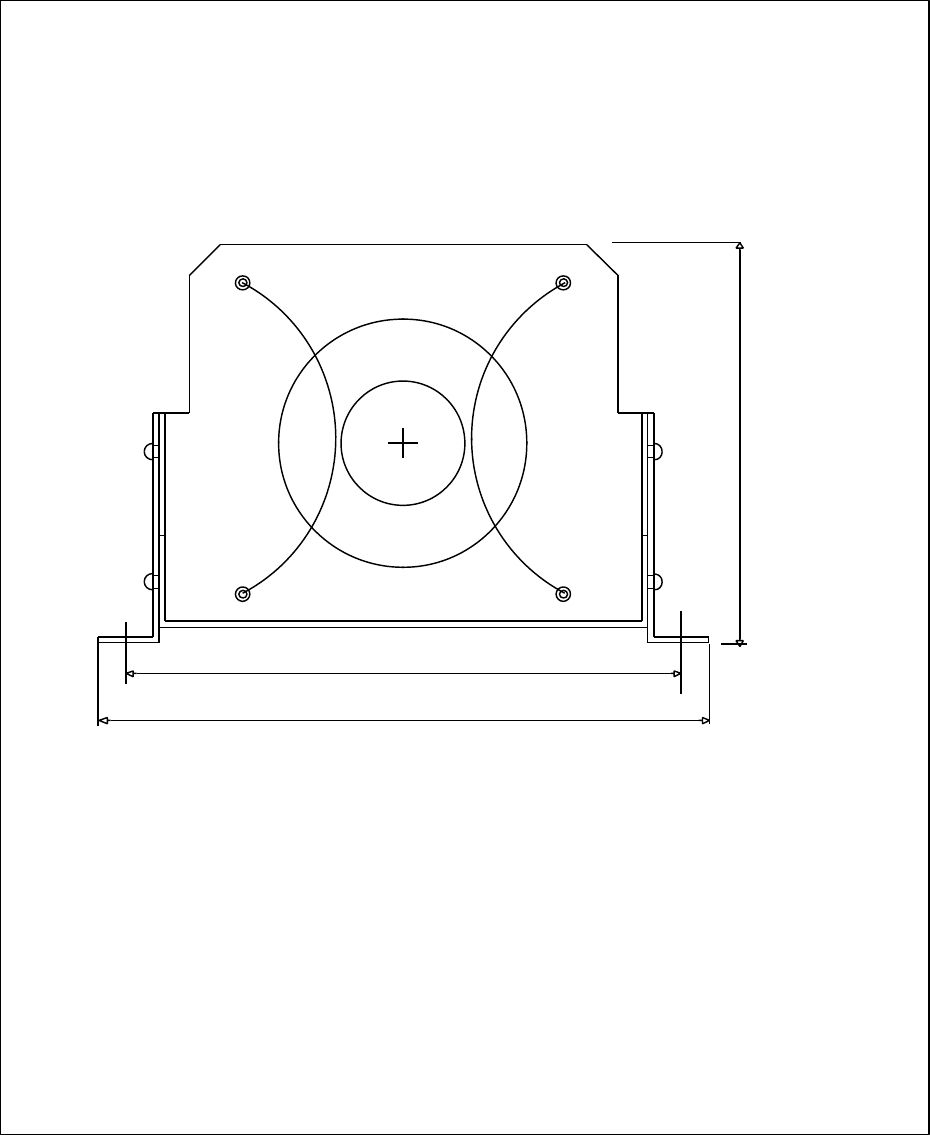
116
DBP - Rev 6/93
FRONT VIEW
182
200
130
DBP6 - SIDE VIEW 1
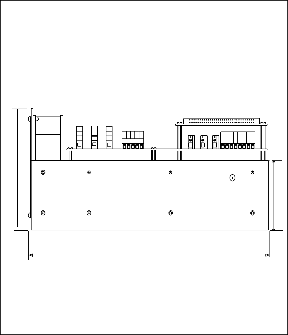
117
DBP - Rev 6/93
DBP6 - SIDE VIEW 2
294
130
75
b
a
1
32
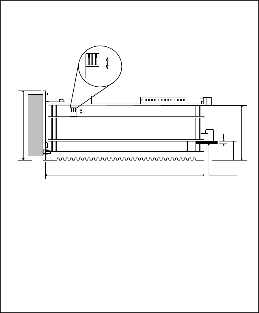
118
DBP - Rev 6/93
RACK 3U/13T
DBP RACK MOUNTING (3U/ 13T)
ON
OFF
12
51.54
17.64
2.4
9.64
162.54 KEYING PIN
ON
OFF
1 2
65.84
SIDE VIEW 1
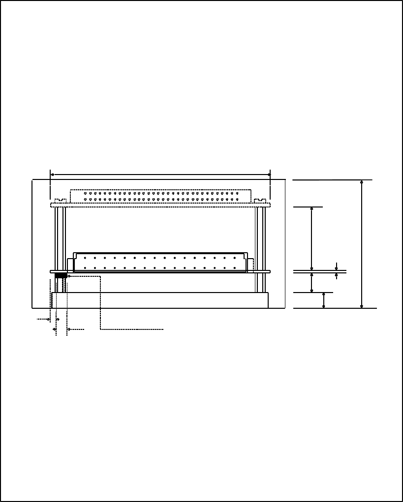
119
DBP - Rev 6/93
DBP RACK MOUNTING (3U/ 13T)
111.76
32.3 65.84
9.64 1.6
8
2C
A
32
KEYING PIN
5.5
3
b
a
1
32
SIDE VIEW 2
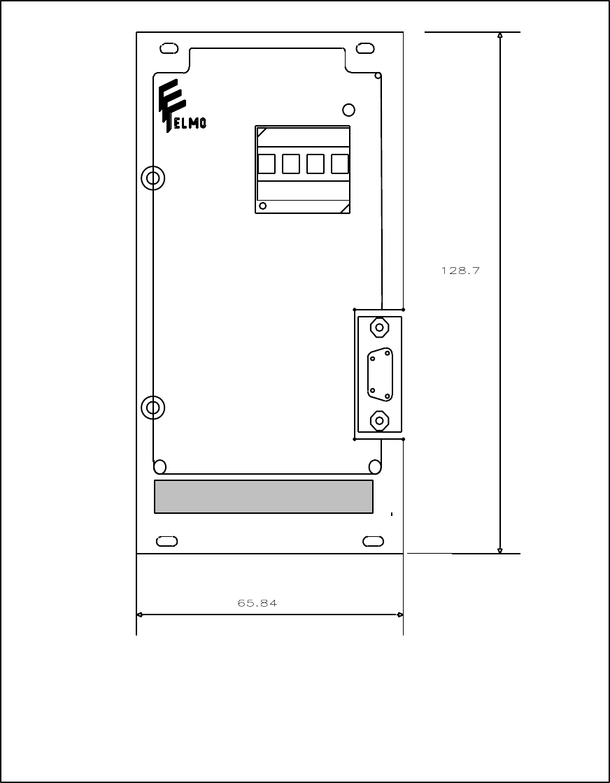
120
DBP - Rev 6/93
POWER
ELMO
FRONT PANEL FOR DBP 3U/13T
95
1
6
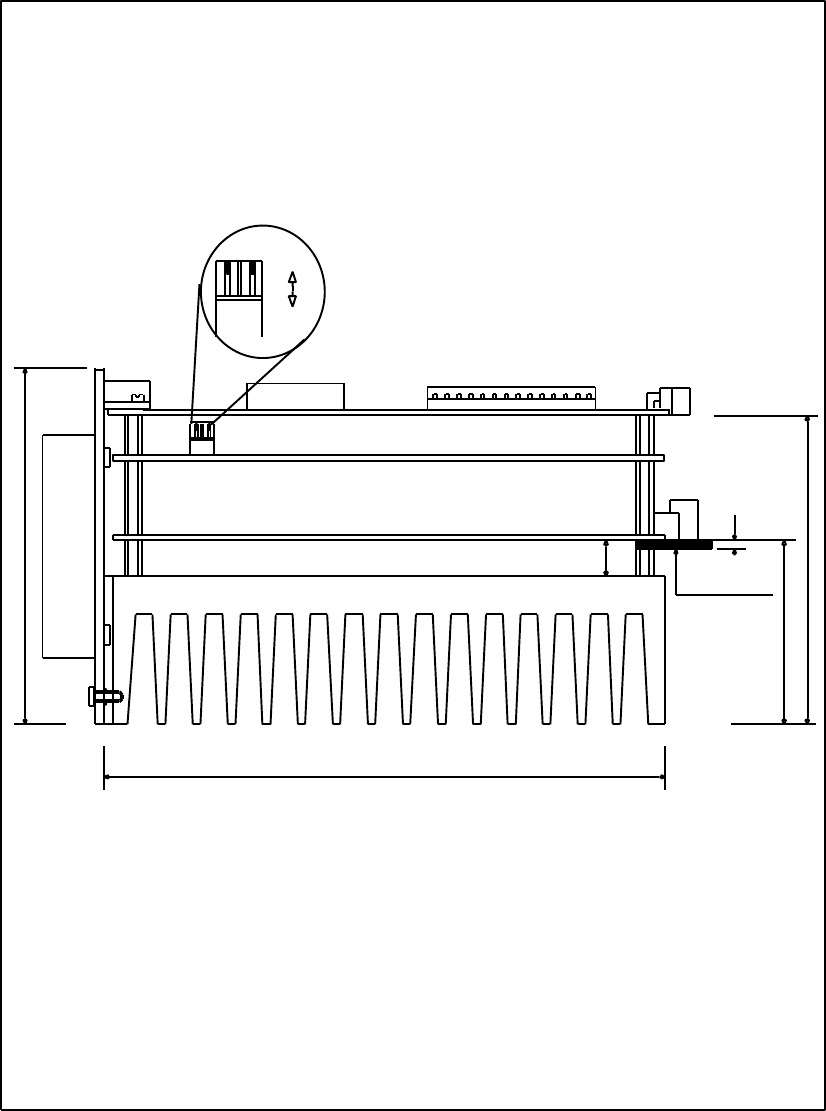
121
DBP - Rev 6/93
RACK 3U/20T
DBP RACK MOUNTING (3U/20T)
1
9.64
2.4
83.54
49.64
KEYING PIN
162.54
ON
OFF
1 2
101.4
SIDE VIEW 1
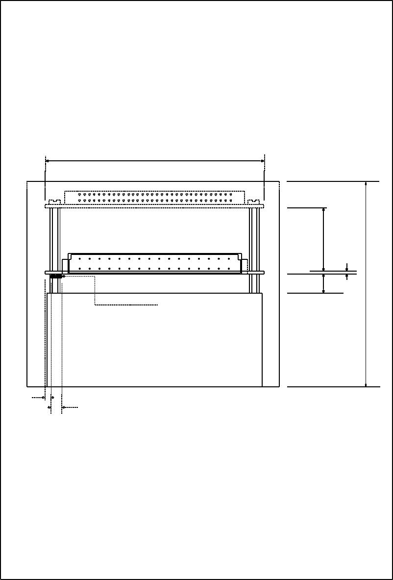
122
DBP - Rev 6/93
DBP RACK MOUNTING (3U/ 20T)
111.76
32.3
32 C
A
2
9.64
1.6
KEYING PIN
3
5.5
b
a
132
101.4
SIDE VIEW 2
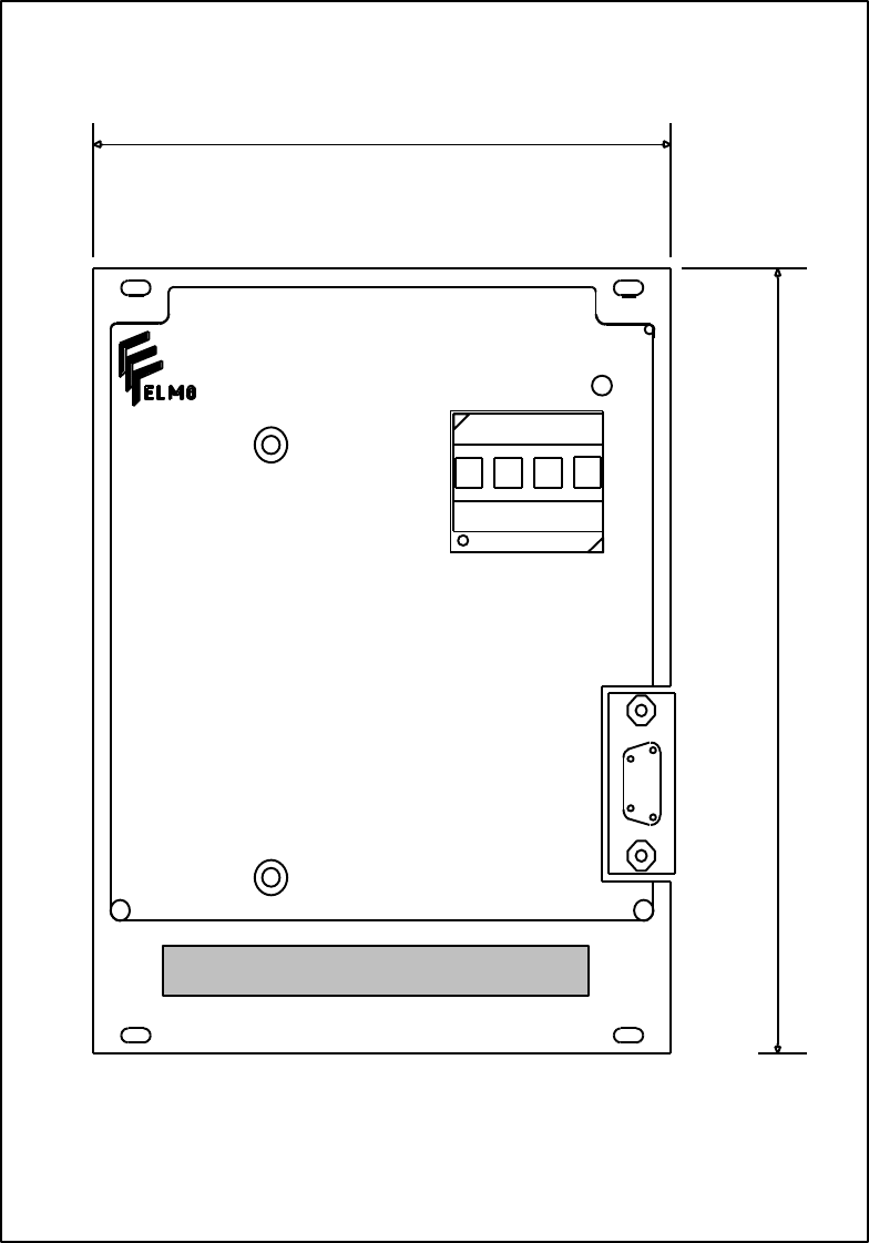
123
DBP - Rev 6/93
101.4
128.7
POWER
ELMO
FRONT PANEL FOR DBP 3U/ 20T
95
1
6
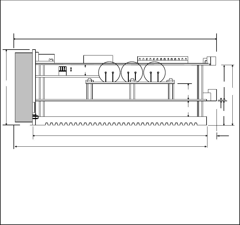
124
DBP - Rev 6/93
RACK 6U/14T
189
ON
OFF
1 2
9.64
14.64
1.6
14.64
32.3
22.64
56.54
162.5
180
8.5
DBP RACK MOUNTING (6U/14T)
70.92
SIDE VIEW 1
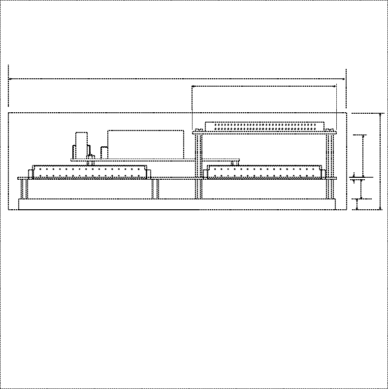
125
DBP - Rev 6/93
32 2C
A32 C
A
2
32.3
1.6
14.6
71
111.76
262
8
DBP RACK MOUNTING (6U/14T)
b
a
1
32
SIDE VIEW 2
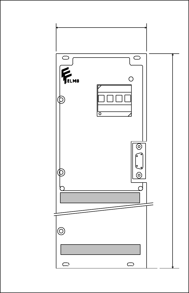
126
DBP - Rev 6/93
70.92
262
FRONT PANEL FOR DBP 6U/14T
POWER
ELMO
95
1
6
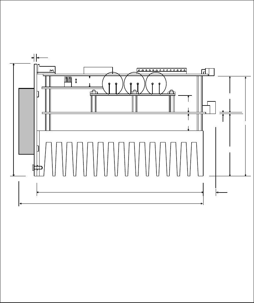
127
DBP - Rev 6/93
RACK 6U/21T
DBP RACK MOUNTING (6U/21T)
9.64
14.64
ON
12
14.64
1.6
88.54
54.64
162.5
32.3
SIDE VIEW 1
180
2.4
8.5
OFF
106.5
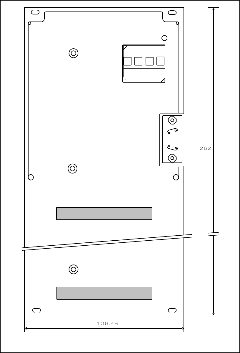
128
DBP - Rev 6/93
POWER
ELMO
FRONT PANEL FOR DBP 6U/21T
95
1
6
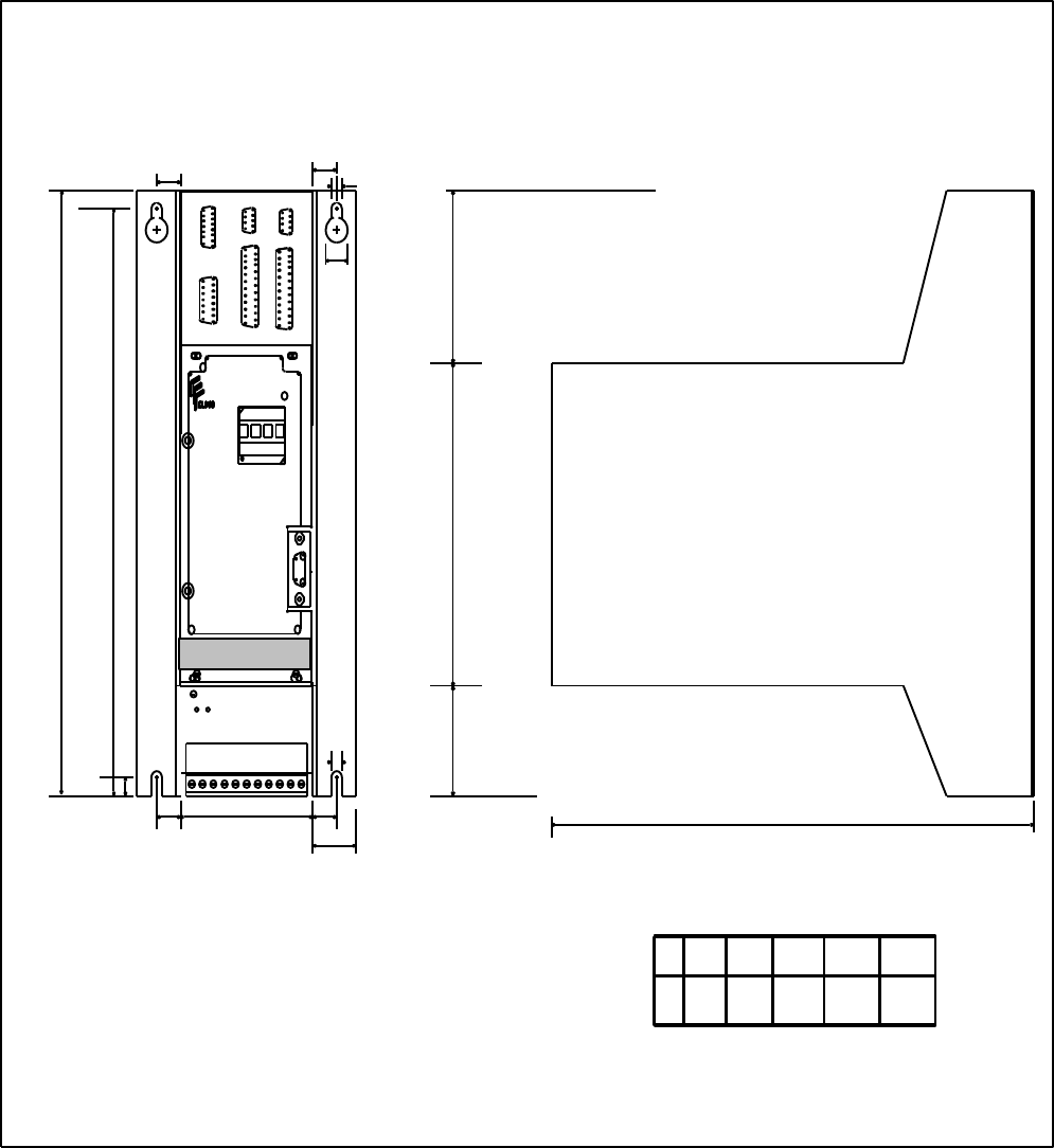
129
DBP - Rev 6/93
ENCD - 3U/...
SIDE VIEW
FRONT VIEW
ENCD - 3U/...
11
11
10
5
95
132.5
265.5
272.5
222
45.0
20
5
11
11 X
POWER
7.5
NOTE:
ALL DIMENSIONS ARE IN mm.
X102.7
12T 20T16T
62.0 82.3
24T 36T
123.0 184.0
Standard Sizes
For non-standard sizes:
X = 5.08 x n + 1mm
POWER
ELMO
95
1
6
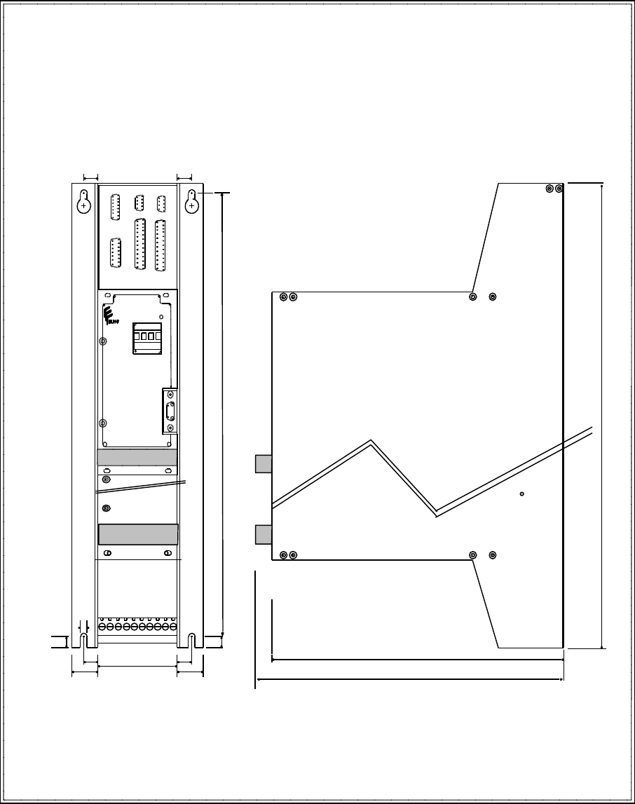
130
DBP - Rev 6/93
ENCD - 6U/...
SIDE VIEW
11
11 FRONT VIEW
5POWER
7.5
11
20
X
11
20
7.5
NOTES: 1. ALL DIMENSIONS ARE IN mm.
2. X = n x 5.08+1, n = number of T
ENCD - 6U/...
222
400
234
406.5
POWER
ELMO
95
1
6
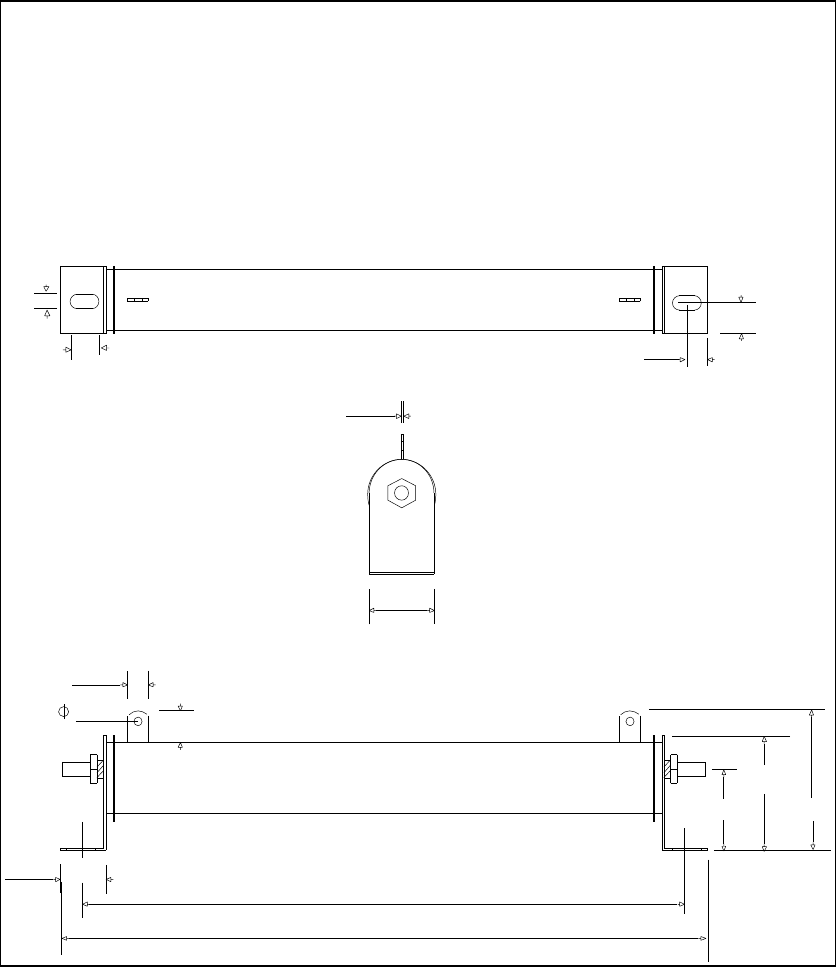
131
DBP - Rev 6/93
EXTERNAL SHUNT RESISTOR
TOP VIEW
11.9
15.9
SIDE VIEW
.508
31.75
FRONT VIEW
9.5
4.4
15.9
38
54
22.2
293.7
EXTERNAL SHUNT RESISTOR (ESR)
14.3
7.14
67
316

132
DBP - Rev 6/93
List of ELMO Service Centers
ISRAEL
Elmo Motion Control LTD
34 Segula ST.
Petah-Tikva 49103
Tel: (03)934-5059
Fax: (03)934-5126
U.S.A
Elmo Motion Control INC.
1200 Woodruff Road, Suite C-22,
Greenville, SC 29607
Tel: (803) 288-9316
Fax: (803) 288-9318
EUROPE
Elmo Motion Control
Stanserstr. 7
CH-6362 Stansstad, Switzerland
Tel: (041) 610775
Fax: (041) 610778
================================================================
AUSTRIA
Kwapil
POB 64
A-1091 Wien
Tel: (0222) 342597
Fax: (0222) 311203
BENELUX
Eltromat B.V.
Looierij 26
4760 AB Zevenbergen
The Netherlands
Tel: (01680) 25925
Telefax: (01680) 28485

134
DBP - Rev 6/93
FINLAND
OY Scandrive
Elsankuja 2 K
SF-02231 Espoo
Tel: 358-0-8035044
Fax: 358-0-8035055
FRANCE
A 2 V SA
11-12 Rue Eugene HENAFF,
78190 Trappes,
Tel: (1) 30620101
Fax: (1) 30626204
GERMANY
IME GmbH
Brugger str. 8
D-78628 Rottweil
Tel: 0741/22091
Fax: 0741/22060
ITALY
Servotecnica SRL
Viale Lombardia 20
20095 Cusano Milanino (MI)
Tel: (02) 66401010
Fax: (02) 66401020
SWEDEN
Aratron AB
P.O.B 20087,
Kratsbodavagen 50,
S-16120 Bromma
Tel: 8-981875
Fax: 8-984281
UNITED KINGDOM
INMOCO Limited
4 Brunel Close
Drayton Fields
Daventry NN11 5LE
Tel: 0327/300320
Fax: 0327/300319
