Enterprise Electronics DTWR-1000C Multi-Mode Radar System User Manual Radar Transmitter Technical Manual
Enterprise Electronics Corporation Multi-Mode Radar System Radar Transmitter Technical Manual
Radar Transmitter Technical Manual
ISSUE/REVISION DATE: June 8, 2000 TECHNICAL MANUAL
VOLUME 2, PART 3
T3-35718 3-3-1
PART 3
TECHNICAL THEORY
CHAPTER 3
TRANSMITTER, EEC-127801-100
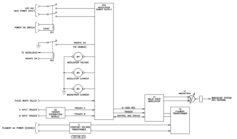
3-3-1 TRANSMITTER BLOCK DIAGRAM DESCRIPTION
Figure 3-3-1 is a block diagram of the transmitter and Figure 3-3-2 is the RF subsystem components.
Both should be referred to during this discussion. The transmitter is located in the transmitter cabinet,
Unit 2, and contains the components that generate RF energy. The word “transmitter” is used to
encompass all the modulator circuitry including the magnetron, and the RF components. Specifically,
the transmitter includes the modulator power supply, solid-state modulator, filament transformer,
magnetron filament filter, constant voltage transformer, magnetron, magnetron and modulator metering
circuits, control circuits, trigger distribution module, control panel, and waveguide components.
Whether in track mode, beacon mode, or weather mode operation, triggering of the transmitter occurs
with the introduction of modulator triggers to the transmitter from within the Tracking Console, Unit 1.
Trigger timing and the selected pulsewidth jointly determine the operating mode of the radar system.
With all the interlock switches closed and the magnetron filament warm-up time expired, relay K5 in the
transmitter will energize applying an enabling ground to the high voltage enable terminal of the
modulator power supply.
FIGURE 3-3-1 TRANSMITTER BLOCK DIAGRAM
ISSUE/REVISION DATE: June 8, 2000 TECHNICAL MANUAL
VOLUME 2, PART 3
T3-35718 3-3-2
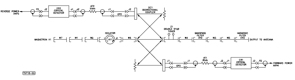
FIGURE 3-3-2 RF SUBSYSTEM BLOCK DIAGRAM
3-3-1-1 TRANSMIT CYCLE
The transmit cycle begins with the generation of a transmitter timing trigger by either an external Radar
Control Processor or Radar Video Processor during normal operation. The transmitter trigger is sent to
the dual-channel trigger distribution module, which is an integral part of the transmitter-receiver, located
in the transmitter cabinet. From the trigger distribution module the modulator power supply module
receives the timing trigger and prepares it to drive the solid-state modulator. The modulator voltage
power supply is regulated to minimize ripple in the transmitter pulse. It uses all solid-state circuitry to
produce the high voltage pulse that is applied to the pulse and filament transformer. The stepped-up
negative output voltage pulse of the pulse and filament transformer, about 38 kV, is then applied to the
magnetron as the modulating pulse.
Using the process just described the transmitter produces high-powered (1 MW) pulses, 2, 1, 0.8, or 0.5
microseconds in duration. The magnetron is driven into oscillation by the high voltage pulse from the
modulator, and produces RF energy at a tunable frequency of 5300 to 5700 MHz. Magnetron output is
coupled to a circulator that permits both transmission and reception through the same waveguide. From
the circulator the energy is transferred through a bidirectional coupler (to permit measurement of
forward power and reverse power) to the antenna.
3-3-1-2 DUAL-CHANNEL TRIGGER DISTRIBUTION MODULE
The trigger distribution module and PCA are shown schematically in Volume 3. The purpose of the
trigger distribution module is to furnish the required triggers to the modulator power supply, AFC
module, test signal generator controller module, sample and hold module and TX/RX BITE module.
3-3-1-3 MAGNETRON
The magnetron is a coaxial cavity type vacuum tube that has a permanent magnet integral to the tube.
When shocked into oscillation by the 38 kV high voltage pulse, the magnetic field causes the stream of
electrons from the cathode to spin at the RF frequency rate. An RF probe picks off the RF energy at the
output and couples it into the waveguide. The magnetron power oscillator is capable of producing 1
MW at 250 PPS and 2 µs pulsewidth with a duty cycle of 0.0005; at 160 PPS and 1 µs pulsewidth with a
duty cycle of 0.00016; at 1180 PPS and 0.8 µs pulsewidth with a duty cycle of 0.00094; and at 320 PPS
and 0.5 µs pulsewidth with a duty cycle of 0.00016. The tube is approximately 50 percent efficient.
3-3-1-4 RF COMPONENTS
Figure 3-3-2 is a block diagram of the RF components. RF energy from the magnetron propagates
through W7, W1, and W2 before it enters 2-port isolator HY1. From the isolator, RF energy is fed into a
sidewall-type bidirectional coupler, DC1. This coupler is characterized by 40 dB directivity, and is used
for forward and reverse power measurements, and other measurements including MDS, pulsewidth, and
RF frequency. From the Bidirectional coupler the RF immediately enters a double-stub tuner, Z1, which
permits adjustment of the waveguide VSWR. Waveguide section W4 connects the double-stub tuner to
HY2, a band-pass filter used to limit out-of-band (spurious) radiation from the system. From HY2, RF
passes through W3 and W5 to the top of the transmitter and harmonic filter HY3. HY3 is used to
ISSUE/REVISION DATE: June 8, 2000 TECHNICAL MANUAL
VOLUME 2, PART 3
T3-35718 3-3-3
attenuate integer multiples of the base transmitter frequency. From the harmonic filter, RF is routed by a
series of waveguide sections to the pedestal and antenna assembly for transmission.
3-3-1-5 SOLID STATE MODULATOR SYSTEM
The solid state modulator system is designed to pulse a C-band magnetron operating under the
following conditions:
Pulse voltage : 38 kV
Pulse current : 60 amps peak
Peak Output power: 1 MW
Duty cycle: .001
RRV: 40-60 kV/µs
Filament Power: 9.0 VDC @ 18 amps
Pulse Conditions: 2.0 µs @ 250 PPS or
1.0 µs @ 160 PPS or
0.8 µs @ 1180 PPS or
0.5 µs @ 320 PPS
The pulse system consists mainly of three self-contained components:
1. Dual-Channel Modulator Power Supply
2. Solid-State Modulator Assembly
3. Magnetron Filament Transformer
3-3-1-5-1 DUAL-CHANNEL MODULATOR POWER SUPPLY
Input power requirements for the modulator power supply are 220 VAC single phase at a nominal 15
amps. Internal design of the power supply is dual channel nonredundant. This means simply that both
channels are required to support dual mode operation and the two sections of the power supply do not
provide backup for each other.
The front panel of the power supply has all of the controls and monitors necessary to ensure proper
operation and adjustments of the system. It also provides a starting point in identifying any problems
which may arise with the modulator section during radar operation. All internal low voltages essential
for operation of the modulator power supply are monitored on the front panel and their presence
indicated by an illuminated LED. Power supply output voltage is controlled by a ten-turn potentiometer
located on the lower right side of the front panel. Above this control is the manual reset button which
allows the power supply to be brought back on line after a predetermined number of fault events have
occurred within an allotted amount of time and faulted out the power supply. These events would
generally be associated with some abnormality in the magnetron tube operation. To the left of the reset
button are two groups of fine adjustment controls for the pulsewidths mentioned earlier (2.0, 1.0, 0.8,
and 0.5 µs), one group is for channel A of the power supply and the other for channel B.
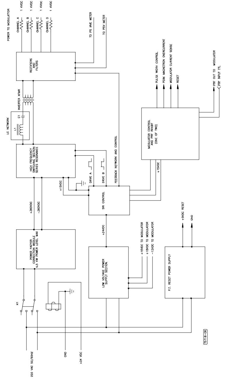
Power supply block diagram, Figure 3-3-3, shows the 220 VAC is switched on to the system via the
activation of +24 VDC. Input power is first applied to a power factor correction system, which
improves the power factor of the system to nearly 98%.
The power level of the power supply is 3.0 kW and also provides auxiliary power to the modulator
section. The block diagram shows the various sections of the power supply.
The power factor system accomplishes the following additional functions:
a. Rectifies and regulates the input power to a DC bus level of 360 VDC
ISSUE/REVISION DATE: June 8, 2000 TECHNICAL MANUAL
VOLUME 2, PART 3
T3-35718 3-3-4
b. It is equipped with a soft-start circuit that regulates the rate of rise of the input
power and charges the main capacitor bank at the nominal input current level.
Main topology of the power system is based on a series resonant circuit with an impedance level that is
set by the power level of the system.
The main inverter section is a half-bridge controlled by a series resonant control circuit. The SRI control
provides drive power to the main bridge at a frequency level proportional to the power level required by
the system. When the system calls for additional power, the main inverter frequency is raised
proportionally to comply with the power demand. Output voltage of the power supply is set at 1000
VDC maximum at 3.0 amps.
Low voltage sections of the power supply, as shown in the main block diagram, provide the following
voltage levels:
a. +15 VDC
b. +18 VDC
c. –12 VDC
There is one additional low voltage power supply of +5 VDC, which provides reset power to the main
pulse transformer system in the main modulator section.
The power supply and the main modulator system communicate through the modulator control circuit
shown in the main power supply block diagram. The modulator control circuit provides the following
functions:
a. Selects and adjusts the various pulse widths for the system.
b. Places the main modulator system in either Standby or Radiate mode.
c. Provides visual display indicating the above mode.
d. Provides protection against peak average overcurrent conditions.
e. Provides visual displays indicating any of the above conditions.
f. Provides protection against improper pulse width and PRF.
g. Turns the power supply off if improper conditions are sustained for a presettable time span.
h. Resets the system back into operation.
The front panel of the power supply contains the following controls and indicators:
a. Six light indicators, which show the status of the system ;
b. Two pulsewidth adjustments ports for the main 0.8 µs and 2.0 µs pulsewidths;
c. A reset button, which resets the power supply;
d. A ten-turn potentiometer, which adjusts the output voltage of the power supply
and thus controls the power level of the modulator system.
The rear panel of the power supply contains the following items:
a. A terminal strip with the following signals:
220 VAC main power input
1000 VDC outputs to the main modulator tank
+5 VDC Reset power supply
+5 VDC Reset power supply return
ISSUE/REVISION DATE: June 8, 2000 TECHNICAL MANUAL
VOLUME 2, PART 3
T3-35718 3-3-5
b. Four fuses for the main and the auxiliary power section of the power supply.
c. Two BNC connectors for the PRF input and the PRF output. The PRF input should connect
to the outside source for the system PRF and the PRF output should connect to the BNC
located in the main modulator tank marked PRF IN.
d. A control connector which is connected to the controls of the system.
e. An auxiliary connector providing low voltage power to the modulator and is connected to the
modulator tank connector marked Control Power.
f. Three fans providing cooling to the power supply.
ISSUE/REVISION DATE: June 8, 2000 TECHNICAL MANUAL
VOLUME 2, PART 3
T3-35718 3-3-6
FIGURE 3-3-3 POWER SUPPLY BLOCK DIAGRAM
ISSUE/REVISION DATE: June 8, 2000 TECHNICAL MANUAL
VOLUME 2, PART 3
T3-35718 3-3-7
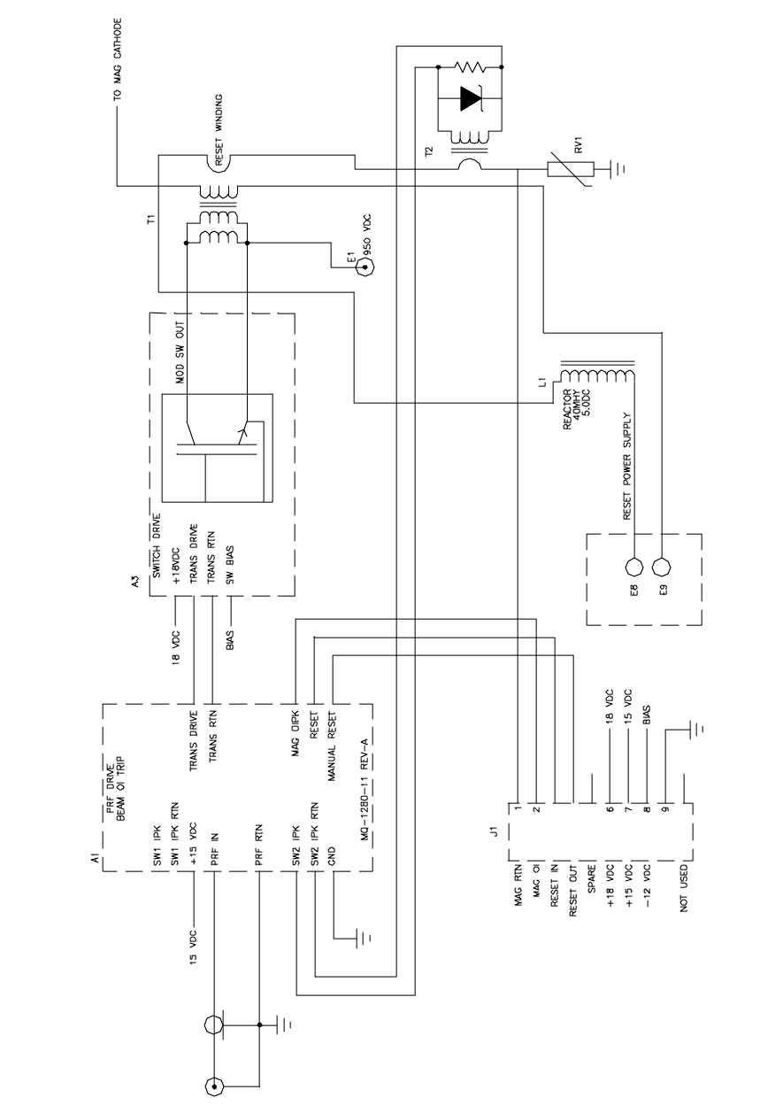
3-3-1-5-2 MODULATOR BLOCK DIAGRAM
A functional block diagram of the modulator is shown in Figure 3-3-4.
The modulator system is housed inside an oiled filled container for cooling and insulating reasons.
The modulator employs state-of-the-art solid-state design using IGBT (insulated gate bipolar transistor)
technology. Recent developments in IGBT technology have made it possible to utilize all solid state
switches to perform all the high energy switching required by the modulator section. The four 1000
VDC lines provided by the power supply are connected to the modulator main switch deck charging the
main capacitor bank of the hard-tube modulator. This energy is then discharged via an IGBT switch into
the primary winding of a high voltage pulse transformer. The length of discharge time is controlled by
the modulator control circuitry of the modulator power supply in order to generate the required 0.5 µs,
0.8 µs, 1.0 µs, and 2.0 µs pulsewidths of the system.
Output of the pulse transformer rises to a pulse amplitude of 38 kV and this is one of the reasons for the
oil environment. The second reason is to provide cooling to the modulator system.
The top section of the modulator tank contains the following:
a. A high voltage connection marked HV Output
b. A BNC Connector marked PRF IN
c. Thirteen terminals whose functions are indicated with the proper markings. All these
terminals are connected to the power supply section. The top part of the terminals marked 1,
2, 6, 7, 8 and 9 are connected to the auxiliary power connector of the power supply. E8 and
E9 connect to the reset terminals on the back section of the power supply. E4, E5, E6, and
E7 are the four 1000 VDC ports and connect to the terminal strip located in the back section
of the power supply. E1 is a ground terminal.
3-3-1-5-3 FILAMENT TRANSFORMER
The filament transformer provides filament power to the magnetron with 50 kVDC isolation between
secondary and primary windings. The power rating of the filament transformer is 9.0 volts DC at 18
amps DC. The filament transformer is oil filled with bushings for the input and output connections. The
high voltage bushing of the filament transformer contains two studs marked Cathode and Heater. Input
voltage to the filament transformer is 220 VAC 50/60 Hz.
The terminal marked cathode should be connected to the output HV terminal of the modulator and the
one marked heater to the magnetron heater lead. The filament transformer is located adjacent to the
modulator in the lower compartment of the system next to the power supply.
ISSUE/REVISION DATE: June 8, 2000 TECHNICAL MANUAL
VOLUME 2, PART 3
T3-35718 3-3-8
FIGURE 3-3-4 MAIN MODULATOR BLOCK DIAGRAM
ISSUE/REVISION DATE: June 8, 2000 TECHNICAL MANUAL
VOLUME 2, PART 3
T3-35718 3-3-9
3-3-2 TRANSMITTER DETAILED DESCRIPTION
The transmitter is shown schematically in Volume 3.
3-3-2-1 INPUT POWER AND CONTROL
Input power for the transmitter and receiver enters at 2J1 to 2TB1 with terminals 1, 2, 3 and 4 the hot
220 voltage (above ground potential), and terminals 5, 6, 7, and 8 to the neutral side of the 220 volts.
2J1 pin C is the ground wire which is connected to ground stud 2E1. The hot voltage is routed through
2F1 (the main power fuse). From 2F1 the voltage is applied to MAIN POWER contactor 2K1-3.
Contactor 2K1 is controlled by 2S1, the transmitter/receiver power switch, and from an external source
(24 VAC) through 2J2 pins A and B.
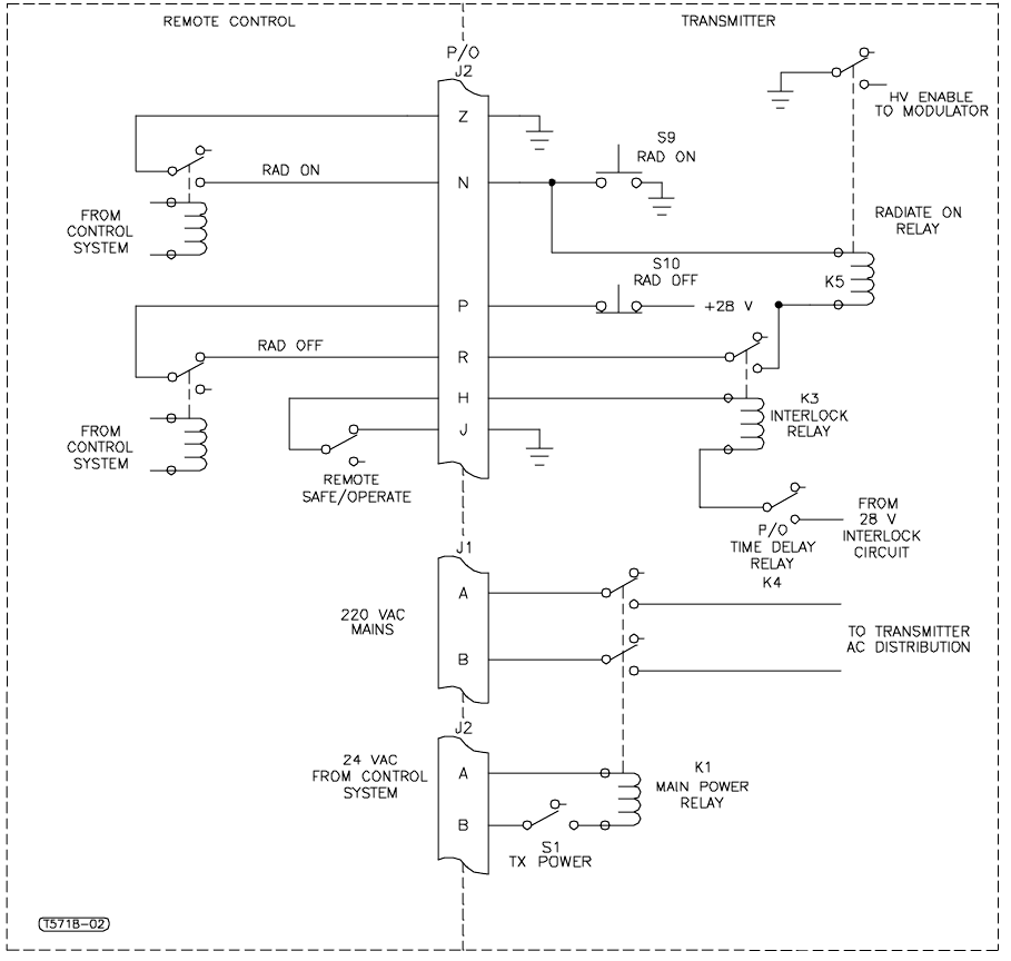
Figure 3-3-5 is a simplified diagram of the transmitter control circuits. The following conditions must
be met prior to placing the transmitter into the RADIATE mode.
♦Servo/RCP power must be ON.
♦Control assembly power must be ON.
♦Transmitter-receiver power must be ON.
♦ Cabinet door and hotbox door interlocks must be closed.
♦Ten minute time delay must be expired.
♦Safety switches at the pedestal and servo cabinet must be in the OPERATE position.
♦Waveguide pressure normal (35 psi)
♦Modulator blowers must be operating
♦Magnetron blower must be operating.
If the above conditions are met, K3 will be energized, lighting the Standby lamps. The RADIATE ON
switch, when depressed, will energize contactor driver relay K5, which in turn will enable the modulator
power supply output to the modulator. This in turn generates the high voltage pulse (normally a
negative 38 kV pulse) to the magnetron, generating the RF pulse to the antenna.
ISSUE/REVISION DATE: June 8, 2000 TECHNICAL MANUAL
VOLUME 2, PART 3
T3-35718 3-3-10
FIGURE 3-3-5 TRANSMITTER CONTROL CIRCUITS
3-3-2-2 MAGNETRON FILAMENTS
Power for the magnetron filaments at 220 VAC is supplied by constant voltage transformer 2T1 and is
then fused by 2F8, a 2 ASB fuse, before being applied to transformer 2T2 the magnetron filament
transformer.
The 220 VAC magnetron filament voltage enters transformer 2T2 at solder lugs 1and 2, through filters
2FL3 and 4, with the 220 VAC hot source routed through filament interlock relay K2 and filament
adjustment rheostat, R1. The other leg of the input AC is routed to the return side of magnetron filament
interlock relay 2K2. This unit protects the magnetron from damage by opening the interlock line when
there is a loss of filament voltage. Inside the assembly, low voltage output from the transformer is
rectified to produce a DC filament voltage which exits at solder lugs C and H (cathode and heater).
3-3-2-3 RUN-TIME METERS
Meter 2M1 is the Operate Time meter and 2M2 is the Radiate Time meter. These cumulative time
meters both operate from 28 VDC inputs. Operate Time is the total time power has been applied to the
ISSUE/REVISION DATE: June 8, 2000 TECHNICAL MANUAL
VOLUME 2, PART 3
T3-35718 3-3-11
transmitter cabinet while Radiate Time is just that portion of the Operate Time that the system has been
radiating (modulator and magnetron working).
3-3-2-4 MODULATOR TRIGGERS
The primary modulator trigger enters the transmitter cabinet at J3 and is routed to the dual-channel
trigger distribution module (A3) at its input A3J2. The secondary modulator trigger enters the
transmitter cabinet at J4 and is also routed to the trigger distribution module at its input A3J3. Output
primary and secondary mod triggers leave the trigger distribution module at J4 and J5 and are applied at
TTL levels to modulator power supply PS4 at J1 and J5 respectively. After conditioning in the
modulator power supply, the modulator triggers leave PS4J2 (A) and J6 (B) and enter the solid-state
modulator at A1JA and A1JB as the modulator pulse.
3-3-2-5 DUAL-CHANNEL TRIGGER DISTRIBUTION MODULE AND PCA (2A3/2A3A1)
Both the dual-channel trigger distribution module and PCA are shown schematically in Volume 3. The
purpose of the trigger distribution module is to furnish the required modulator triggers to the modulator
power supply, and auxiliary (test) primary and secondary modulator triggers to other parts of the system
like the BITE subsystem.
Primary modulator trigger enters the PCA at E1 and the secondary modulator trigger enters at E2. Each
signal is fed directly to the input of a Schmidt trigger inverter, U1. Out of the inverter each trigger
drives three 75 Ω line driver circuits at U2 and U3. Three conditioned primary triggers are output from
the PCA at E5, E9, and E10 leaving the module at jacks J4, J6, and J7. Secondary triggers leave the
PCA at E7, E8, and E11; and the module at jacks J5, J8, and J9.
Input DC power at +15 volts is regulated down to +5 VDC by a circuit card mounted IC regulator and
filter network. Operation of all the trigger distribution module PCA circuitry is from this five volt
source.
3-3-3 TRANSMITTER FAULT MONITORING SUBSYSTEM GENERAL DESCRIPTION
(2A4)
The fault monitoring equipment is a subsystem contained in a single module which, when supported by
the system software, allows important system parameters to be monitored on a continuous basis. The
fault monitoring equipment and support software enhances system performance in that the operator and
technical staff are alerted to any conditions that could potentially degrade system performance and/or the
integrity of acquired data.
The fault monitoring equipment is an integrated subsystem which in no way affects the normal operation
of the radar system.
ISSUE/REVISION DATE: June 8, 2000 TECHNICAL MANUAL
VOLUME 2, PART 3
T3-35718 3-3-12
3-3-3-1 FAULT MONITORING SUPPORT SOFTWARE
The transmitter BITE module is supported by software routines that are fully integrated with the system
software. Software enhancements are also included for the standard radar data display software to allow
the passage of status data as well as the presentation of fault data on the terminal.
3-3-3-2 TRANSMITTER BITE MODULE, EEC-127798-100
The transmitter BITE module primarily samples, conditions, and analyzes important transmitter
parameters to ensure that the system is operating within the bounds of defined specifications. This is an
ongoing, fully-automatic function. In addition, the transmitter BITE module can provide specific
parameter measurement, analysis, and reporting.
The BITE module is equipped to monitor the following types of signals:
♦Two trigger channels
♦Four analog channels
♦Ten logic channels
♦Two power channels
Specifically, the following transmitter parameters are monitored:
a. Power supply voltages
♦TX/RCVR +15 volts (BITE)
♦TX/RCVR -15 volts (BITE)
♦TX/RCVR +28 volts (control voltage)
♦TX/RCVR +15 volts (trigger module)
b. Transmitter RF power
♦Forward Power
♦Reverse Power
c. Trigger
♦Primary transmitter trigger
♦Secondary transmitter trigger
d. Pulsewidth selection status
♦Pulsewidth select status #2
♦Pulsewidth select status #3
♦Pulsewidth select status #4
e. General system performance parameters
♦Interlock status
♦Standby status
♦Radiate status
♦Low airflow
♦Low waveguide pressure
♦Modulator normal
♦Cabinet over-temperature
ISSUE/REVISION DATE: June 8, 2000 TECHNICAL MANUAL
VOLUME 2, PART 3
T3-35718 3-3-13
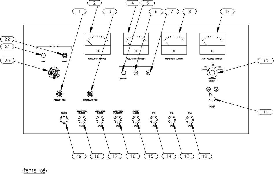
FIGURE 3-3-6 TRANSMITTER CONTROL PANEL, UNIT 2
TABLE 3-3-1 TRANSMITTER CONTROL PANEL UNIT 2
REFERENCE
FIG. 3-3-6 CONTROL OR INDICATOR FUNCTION
1 PRIMARY TRIG jack Provides a test jack to monitor, or use, the
PRIMARY system trigger.
2 MOD HIGH VOLTAGE meter Displays the value of voltage applied to the
modulator.
3 SECONDARY TRIG jack Provides a test jack to monitor, or use, the
SECONDARY system trigger.
4 MODULATOR CURRENT meter Displays the value of the modulator current.
5 STANDBY indicator Indicates that the time delay has expired,
interlocks are closed, and the system is ready to
Radiate.
6 RADIATE OFF Places the transmitter in the Standby mode
when depressed.
ISSUE/REVISION DATE: June 8, 2000 TECHNICAL MANUAL
VOLUME 2, PART 3
T3-35718 3-3-14
TABLE 3-3-1 TRANSMITTER CONTROL PANEL, UNIT 2 (CONT.)
REFERENCE
FIG. 3-3-6 CONTROL OR INDICATOR FUNCTION
7 RADIATE ON Places the transmitter in the Radiate
mode when depressed.
8 MAGNETRON CURRENT meter Displays the average value of magnetron
current.
9 LOW VOLTAGE MONITOR Indicates normal transmitter-receiver DC
meter voltages in green region, and abnormal
values in the red regions. Voltages applied
by use of the voltage select switch.
10 VOLTAGE SELECT switch Selects the voltage to be applied to the
low voltage monitor meter.
11 POWER switch Turns the transmitter main power ON or OFF, if
the MAIN POWER switch at the operating
console is ON.
12 PS3, +15 VDC POWER A .5 ASB fuse that protects the +15
SUPPLY fuse VDC used in the transmitter-receiver
electronics.
13 PS2, +28 VDC POWER A .5 ASB fuse that protects the +28
SUPPLY fuse VDC used in the transmitter-receiver
electronics.
14 PS1, ±15 VDC POWER A 1 ASB fuse that protects the ±15 VDC
SUPPLY fuse used in the transmitter BITE electronics.
15 CABINET BLOWER fuse A 2 ASB fuse that protects the cabinet blowers
located at the top of the cabinet and in HV
compartment enclosure.
16 MAGNETRON FILAMENTS fuse A 2 ASB fuse that protects the 110 VAC input
to the magnetron filament transformer.
17 MODULATOR BLOWER fuse A 1 ASB fuse that protects the hotbox
blower.
18 MAGNETRON BLOWER fuse A 1.5 ASB fuse that protects the magnetron
blower.
19 MAIN POWER fuse/ A blown-fuse indicator for the 30 AMP fuse
indicator that protects the main power into the
transmitter.
ISSUE/REVISION DATE: June 8, 2000 TECHNICAL MANUAL
VOLUME 2, PART 3
T3-35718 3-3-15
TABLE 3-3-1 TRANSMITTER CONTROL PANEL, UNIT 2 (CONT.)
REFERENCE
FIG. 3-3-6 CONTROL OR INDICATOR FUNCTION
20 Intercom Sonalert Produces an audible tone when telephone
RING at the pedestal is depressed.
21 RING switch A momentary push-button switch that
causes the Sonalert at the pedestal to
produce audible tone.
22 Phone jack Enables a sound-powered headset to be
connected for communication to the
pedestal.
ISSUE/REVISION DATE: June 8, 2000 TECHNICAL MANUAL
VOLUME 2, PART 3
T3-35718 3-3-16
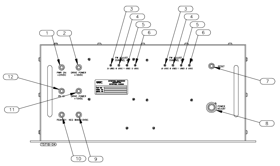
FIGURE 3-3-7 MODULATOR POWER SUPPLY CONTROL PANEL
TABLE 3-3-2 MODULATOR POWER SUPPLY CONTROL PANEL (2PS4)
REFERENCE
FIG. 3-3-7 CONTROL OR INDICATOR FUNCTION
1 Power On Indicator +24 Indicates power has been applied and that the
VDC (Green) +24 VDC power supply is normal when
illuminated.
2 Drive Power +18 VDC Indicates that the drive power +18 VDC is
Indicator (Green) normal when illuminated.
3 PW adjust (.5 µs) Two controls, an A channel and a B channel,
allow for fine adjustment of the .5 µs
pulsewidth from either channel of the modulator
power supply.
4 PW adjust (.8 µs) Two controls, an A channel and a B channel,
allow for fine adjustment of the .8 µs
pulsewidth from either channel of the modulator
power supply.
5 PW adjust (1 µs) Two controls, an A channel and a B channel,
allow for fine adjustment of the 1 µs pulsewidth
from either channel of the modulator power
supply.
ISSUE/REVISION DATE: June 8, 2000 TECHNICAL MANUAL
VOLUME 2, PART 3
T3-35718 3-3-17
TABLE 3-3-2 MODULATOR POWER SUPPLY CONTROL PANEL (CONT.)
REFERENCE
FIG. 3-3-7 CONTROL OR INDICATOR FUNCTION
6 PW adjust (2 µs) Two controls, an A channel and a B channel,
allow for fine adjustment of the 2 µs pulsewidth
from either channel of the modulator power
supply.
7 Reset When depressed will reset either the
power supply overcurrent (PS OI) or the
peak overcurrent (PEAK OI).
8 Power adjust Controls the voltage out of the modulator
power supply that is applied to the modulator,
nominally 1000 VDC.
9 Neg Bias -12 VDC Indicates that the neg bias -12 VDC power
Indicator (Green) is normal when illuminated
10 Peak OI indicator (Red) Indicates the maximum peak current has been
exceeded when illuminated. Has auto reset for
5 faults, then must be reset by the reset switch.
11 Drive Power +15 VDC Indicates that the drive power +15 VDC is
(Green) normal when illuminated
12 PS OI Indicator (Red) Indicates the maximum average current has
been exceeded when illuminated. Has auto
reset for 5 faults, then must be reset by the reset
switch.