Contents
- 1. User manual 1
- 2. User manual 2
User manual 1
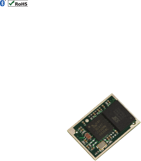
BTM410/411
DATA MODULE
USER MANUAL
Innovative Technology
for a Connected World
www.lairdtech.com
2
www.lairdtech.com
Laird Technologies
BTM410/411
Bluetooth® AT Data Module
REVISION HISTORY
Revision Description
REVISION
HISTORY
3
www.lairdtech.com
Laird Technologies
BTM410/411
Bluetooth® AT Data Module
CONTENTS
BTM410/411 Bluetooth® Module ..4
Overview .............................................. 4
BTM410/411 Key Features ................... 4
Specications ................................5
Detailed Specications ......................... 5
Pin Denitions ...................................... 7
Operating Parameters ...................8
Voltage Specications .......................... 8
Conguring the BTM410/411 ........9
AT Command Set .............................. 10
Assumptions ...................................... 10
Commands ........................................ 10
Unsolicited Responses ........................ 30
Incoming Connections ........................ 31
Pairing and Trusted Devices ............... 32
Error Responses .................................. 33
Factory Default Mode ........................ 34
Miscellaneous Features ....................... 34
Disclaimers ......................................... 35
Application Examples ..................36
RS232 Modem Signals ....................... 36
Modem Signaling over Bluetooth® ..... 37
Pure Cable Replacement Mode .......... 37
Audio Cable (Voice) ........................... 38
Modem Control and Status Signals .... 39
Mechanical Drawings ..................40
Mechanical Details ............................. 40
Recommended PCB Footprint ............ 41
Notes for PCB Layout ......................... 41
Diagrams ............................................ 42
Ordering Information ..................44
Product Part Numbers ........................ 44
General Comments ............................ 44
TABLE OF
CONTENTS
4
www.lairdtech.com
Laird Technologies
BTM410/411
Bluetooth® AT Data Module
FEATURES AND BENEFITS
• Bluetooth® v2.1+EDR
• Adaptive Frequency Hopping to cope with interference
from other wireless devices
• Secure Simple Pairing support
• External or internal antenna options
• Comprehensive AT interface for simple programming
• Bluetooth® END Product Qualied
• Compact size
• Class 2 output – 4dBm
• Low power operation
• UART interface
• Multi-point support
• PCM and SCO for external codec
• GPIO lines under AT control
• Support for Serial Port Prole
• Support for Health Device Prole (Q3 ‘09)
• Wi-Fi co-existence
APPLICATION AREAS
• Embedded Devices
• Phone Accessories
• Security Devices
• Medical and Wellness
Devices
• Automotive Applications
• Bluetooth® Advertising
• ePOS
The BTM410 and BTM411 Bluetooth® modules from Laird Technologies have been designed to meet the
needs of developers who wish to add robust, short range Bluetooth data connectivity to their products. They
are based on the market leading Cambridge Silicon Radio BC04 chipset, providing exceptionally low power
consumption with outstanding range. They support the latest Bluetooth® Version 2.1 Specication, providing
the important advantage of Secure Simple Pairing, which improves security and enhances the ease of use for
end customers.
With physical sizes as small as 12.5 x 18.0mm and best of class, low-power operation, these modules are the ideal
choice for applications where designers need both performance and minimum size. For maximum exibility in
systems integration, the modules are designed to support a separate power supply for I/O.
To aid product development and integration, Laird Technologies has integrated a complete Bluetooth protocol
stack within the modules, including support for the Bluetooth Serial Port Prole. The modules are fully qualied as
Bluetooth End Products, allowing designers to integrate them within their own products with no further Bluetooth
Qualication. They can then list and promote their products on the Bluetooth website free of charge.
Future releases include support for the Bluetooth Health Device Prole, making this module the ideal choice for
manufacturers who are developing Continua Health Alliance
compliant devices.
A comprehensive AT command interface is included, which simplies rmware integration. Combined with a low
cost developers kit, this ensures that the choice of Laird Technologies Bluetooth modules guarantees the fastest
route to market.
OVERVIEW AND
KEY FEATURES

5
www.lairdtech.com
Laird Technologies
BTM410/411
Bluetooth® AT Data Module
CATEGORIES FEATURE IMPLEMENTATION
Wireless Specication Bluetooth®Version 2.1+EDR
Transmit Class Class 2
Frequency 2.402 – 2.480 GHz
Channels 79 channels Frequency Hopping
Adaptive Frequency Hopping
Max Transmit Power +4 dBm at antenna pad – BTM410
+4 dBmi from integrated antenna – BTM411 (provisional)
Min Transmit Power
-27 dBm at antenna pad – BTM410
-27 dBmi from integrated antenna – BTM411
(provisional)
Receive Sensitivity -84dBm
Range Up to 50 metres free space
Data Transfer Rate Up to 300 kbps
Antenna Modes External Antenna 50 Ohm matched SMT pad – BTM410
Integrated Antenna (option) +0dBi multilayer ceramic – BTM411 (provisional)
UART Interface Serial Interface RS-232 bi-directional for commands and data
16550 compatible
Baud Rate Congurable from 1,200 to 921,600bps Non-standard
baud rates supported
Bits 8
Parity Odd, even, none
Stop bits 1 or 2
Default Serial parameters 9600,n,8,1
Levels Set by VDD_USB input
Modem Control DTR, DSR, DCD, RI, RTS, CTS
General Purpose Interface I/O 8 general purpose I/O pins
Audio Support 3 PCM Channels @ 64kbps
SCO Channels Support SCO and eSCO
PCM Interface
Congurable as master or slave
8 bit A-law
8 bit μ-law
13 bit linear
PCM Clock available when in slave mode
Protocols and Firmware Bluetooth Stack V2.1 compliant. Fully integrated.
Proles
GAP (Generic Access Prole)
SDP (Service Discovery Prole)
SPP (Serial Port Prole)
HDO (Health Device Prole) – 2009 release
Firmware Upgrade Available over UART
Connection Modes Point to point (cable replacement)
Multipoint – max 3 slaves
SPECIFICATIONS

6
www.lairdtech.com
Laird Technologies
BTM410/411
Bluetooth® AT Data Module
CATEGORIES FEATURE IMPLEMENTATION
Command Interface AT Instructions set Comprehensive control of connection and module operation
S Registers for non-volatile storage of parameters
Multipoint Software Supports multiple connections
Current Consumption Data Transfer Typically 32mA
Low Power Sniff Mode Less than 2.5mA
Supply Voltage Supply 3.0V – 3.3V DC
I/O 1.7V – 3.3V DC (independent of Supply)
USB & UART 1.7V – 3.6V DC (independent of Supply)
Coexistence / Compatibility WLAN (802.11) 2-wire and 3-wire hardware coexistence
schemes supported
Connections Interface Surface Mount Pads
External Antenna (BTM410) Pad for 50 Ohm antenna
Physical Dimensions 12.5mm x 18.0 x 1.6mm BTM410
12.5mm x 24.0mm x 1.6mm BTM411 (provisional)
Weight 3 grams
Environmental Operating Temperature -30°C to +70°C
Storage Temperature -40°C to +85°C
Approvals Bluetooth Qualied as an END product
FCC
Meets FCC requirements
Modular Approval
(Integrated Antenna option – BTM411)
CE & R&TTE Meets CE and R&TTE requirements
Miscellaneous Lead free Lead-free and RoHS compliant
Warranty 12 Months
Development Tools Development Kit
Development board and software tools
DVK-BTM410 Dev Kit with BTM410 module tted
DVK-BTM411 Dev Kit with BTM411 module tted
SPECIFICATIONS

7
www.lairdtech.com
Laird Technologies
BTM410/411
Bluetooth® AT Data Module
PIN SIGNAL DESCRIPTION VOLTAGE
SPECIFICATION
1 Unused
2 GND
3 UART_CTS Clear to Send I/P VUSB
4 UART_RXD Receive data I/P VUSB
5 UART_RTS Request to Send O/P VUSB
6 UART_TXD Transmit data O/P VUSB
7 GND
8 SPI_CSB SPI bus chip select I/P VIO
9 SPI_MISO SPI bus serial O/P VIO
10 SPI_MOSI SPI bus serial I/P VIO
11 SPI_CLK SPI bus clock I/P VIO
12 VDD_USB USB & UART supply voltage
13 VDD_IO I/O supply voltage
14 VDD_IN Main supply voltage
15 GND
16 PCM_IN PCM clock I/P VIO
17 PCM_SYNC PCM sync I/P VIO
18 PCM_CLK PCM clock I/P VIO
19 PCM_OUT PCM Data O/P VIO
20 RESET Module reset I/P See note 2
21 GPIO5 I/O for host VIO
22 GPIO3 / UART_DCD I/O for host VIO
23 GND
24 Unused
25 Unused
26 Unused
27 Unused
28 GND
29 ANT (BTM410) Antenna connection (50 ohm matched)
30 GND
31 Unused
32 Unused
33 Unused
34 Unused
35 Unused
36 Unused
37 Unused
38 Unused
39 Unused
40 Unused
41 GND
42 GPIO2 / UART_RI I/O for host VIO
43 GPIO9 /UART_ DTR I/O for host VIO
44 GPIO10 / UART_DSR I/O for host VIO
45 GND
46 D- Not used for AT module variants VUSB
47 D+ Not used for AT module variants VUSB
48 GPIO7 I/O for host VIO
49 GPIO6 I/O for host VIO
50 GPIO4 I/O for host VIO
Note: 1. Unused pins may have internal connections and must not be connected.
2. Reset input is active low. Input is pulled up to VDD_IN via 22k. Minimum reset pulse width is 5ms.
SPECIFICATIONS

8
www.lairdtech.com
Laird Technologies
BTM410/411
Bluetooth® AT Data Module
OPERATING PARAMETERS
RECOMMENDED OPERATING CONDITIONS
OPERATING CONDITION MIN MAX
VDD_USB
(USB compatibility not required) 1.7 3.6
VDD_USB
(USB compatibility required) 3.1 3.6
VDD_IO 1.7 3.3
VDD_IN 3.0 3.3
VOLTAGE SPECIFICATIONS
LOGIC LEVELS (VUSB)
INPUT VOLTAGE LEVELS MIN TYP MAX
Vih 0.7VDD_IO
Vil 1.7<VDD_USB<1.9 -0.4 +0.8
2.7<VDD_USB<3.0 -0.4 +0.4
OUTPUT VOLTAGE LEVELS (1.7<VDD_USB<1.9)
Voh (Iout = -4mA) VDD_USB – 0.4
Vol (Iout = 4mA) 0.4
OUTPUT VOLTAGE LEVELS (2.7<VDD_USB<3.0)
Voh (Iout = -4mA) VDD_USB – 0.2
Vol (Iout = 4mA) 0.2
Note: VDD_USB must be connected to power the USB and UART interfaces.
LOGIC LEVELS (VIO)
INPUT VOLTAGE LEVELS MIN TYP MAX
Vih 0.7VDD_IO
Vil -0.4 +0.8
-0.4 +0.4
OUTPUT VOLTAGE LEVELS (1.7 < VDD_IO < 1.9)
Voh (Iout = -4mA) VDD_IO – 0.4
Vol (Iout = 4mA) 0.4
OUTPUT VOLTAGE LEVELS (2.7 < VDD_IO < 3.0)
Voh (Iout = -4mA) VDD_IO – 0.2
Vol (Iout = 4mA) 0.2
OPERATING
PARAMETERS

9
www.lairdtech.com
Laird Technologies
BTM410/411
Bluetooth® AT Data Module
INTRODUCTION
This document describes the protocol used to control and congure the BT Data Bluetooth device.
The protocol is similar to the industry standard Hayes AT protocol used in telephony modems which is
appropriate for cable replacement scenarios, as both types of devices are connection oriented. The telephony
commands have been extended to make the device perform the two core actions of a Bluetooth device, which
is make/break a connection and Inquiry. Many other AT commands are also provided to perform
ancillary functions, such as, pairing, trusted device database management and S Register maintenance.
Just like telephony modems, the device powers up in an unconnected state and will only respond via
the serial interface. In this state the device will not even respond to Bluetooth Inquiries. Then, just like
controlling a modem, the host can issue AT commands which map to various Bluetooth activities. The
command set is extensive enough to allow a host to make connections which are authenticated and/or
encrypted or not authenticated and/or encrypted or any combination of these. Commands can be saved,
so that on a subsequent power up the device is discoverable or automatically connects.
The device has a serial interface which can be congured for baud rates from 1200 up to 921600 (default
setting is 9600) and an RF communications end point. The latter has a concept of connected and unconnected
modes and the former will have a concept of command and data modes. This leads to the matrix of states
shown below.
RF UNCONNECTED RF CONNECTED
Local Command Mode OK OK
Remote Command Mode ILLEGAL OK
Data Mode ILLEGAL OK
The combinations, ‘Data and RF Unconnected Mode’ and ‘Remote Command and RF Unconnected Mode’
do not make sense and will be ignored.
Navigation between these states is done using the AT commands which are described in detail in
subsequent sections.
CONFIGURING
THE BTM410/411

10
www.lairdtech.com
Laird Technologies
BTM410/411
Bluetooth® AT Data Module
AT COMMAND SET
Assumptions
The CSR (Cambridge Silicon Radio) Bluecore chipset in Laird Technologies devices is memory resource limited.
Therefore it is NOT proposed that there be full implementation of the AT protocol as seen in modems. The
claim made for this device is that it will have a protocol similar to an AT modem. In fact, the protocol is similar
enough so that existing source code written for modems, can be used with very little modication with a Laird
Technologies device.
Therefore the following assumptions are made:
1. All commands are terminated by the carriage return character 0x0D, which is represented by the
string <cr> in descriptions below this cannot be changed.
2. All responses from the device have carriage return and linefeed characters preceding and
appending the response. These dual character sequences have the values 0x0D and 0x0A respectively
and shall be represented by the string <cr,lf>.
3. All Bluetooth addresses are represented by a xed 12 digit hexadecimal string, case insensitive.
4. All Bluetooth Device Class codes are represented by a xed 6 digit hexadecimal string, case insensitive.
Commands
This section describes all available AT commands. Many commands require mandatory parameters and some
take optional parameters. These parameters are either integer values, strings, Bluetooth addresses or device
classes. The following convention is used when describing the various AT commands.
<bd_addr> A 12 character Bluetooth address consisting of ASCII characters ‘0’ to ‘9’, ‘A’ to ‘F’ and ‘a’ to ‘f’.
<devclass> A 6 character Bluetooth device class consisting of ASCII characters ‘0’ to ‘9’, ‘A’ to ‘F’ and ‘a’ to ‘f’.
N A positive integer value.
M An integer value which could be positive or negative, which can be entered as a decimal value or
in hexadecimal if preceded by the ‘$’ character. E.g. the value 1234 can also be entered as $4D2
<string> A string delimited by double quotes. E.g. “Hello World”. The “ character MUST be supplied as delimiters.
<uuid> A 4 character UUID number consisting of ASCII characters ‘0’ to ‘9’, ‘A’ to ‘F’ and ‘a’ to ‘f’.
1. ^^^ {Enter Local Command Mode}
When in data and connected mode, the host can force the device into a command and connected
mode so that AT Commands can be issued to the device. The character in this escape sequence is
specied in the S2 register, so can be changed. In addition, the escape sequence guard time is
specied by S Register 12. By default the guard time is set to 100 milliseconds. Please refer to
Section 5: Dropping Connections for more related information.
In modems this escape sequence is usually “+++”. “^^^” is specied to avoid confusion when the
module is providing access to a modem.
Response: <cr,lf>OK<cr,lf>
2. !!! {Enter Remote Command Mode}
When in data and connected mode, the host can force the remote device into a command and
connected mode so that AT Commands can be issued to the device remotely. The escape sequence
guard time is specied by S Register 12 and is the same as per the ^^^ escape sequence. By default
the guard time is set to 100 milliseconds. The remote device issues ATO as normal to return to data
mode. (Refer to step 12)
For this command to be effective S Register 536 must be set to 1.
Response: <cr,lf>OK<cr,lf>
CONFIGURING
THE BTM410/411

11
www.lairdtech.com
Laird Technologies
BTM410/411
Bluetooth® AT Data Module
CONFIGURING
THE BTM410/411
3. AT
Used to check the module is available.
Response: <cr,lf>OK<cr,lf>
4. ATA {Answer Call}
Accept an incoming connection, which is indicated by the unsolicited string
<cr,lf>RING 123456789012<cr,lf> every second. 123456789012 is the Bluetooth address of the
connecting device.
Response: <cr,lf>CONNECT 123456789012<cr,lf>
5. ATD<U><Y><bd_addr>,<uuid> {Make Outgoing Connection}
Make a connection to device with Bluetooth address <bd_addr> and SPP prole <uuid>. The <uuid>
is an optional parameter which species the UUID of the prole server to attach to, and if not supplied
then the default UUID from S Register 101 is used. As this is a device which utilises the RFCOMM
layer as described in the Bluetooth specication, it necessarily implies that only proles based on
RFCOMM can be accessed.
If <U> is not specied, then authentication is as per register 500, otherwise the connection will
be authenticated.
If <Y> is not specied, then encryption is as per register 501, otherwise the connection will have
encryption enabled.
The timeout is specied by S register 505.
Response: <cr,lf>CONNECT 123456789012<cr,lf>
Or <cr,lf>NO CARRIER<cr,lf>
Due to a known issue in the Bluetooth RFCOMM stack, it is not possible to make more than 65525
outgoing connections in a single power up session. Therefore if that number is exceeded, then the
connection attempt will fail with the following response:-
Response: <cr,lf>CALL LIMIT
Or <cr,lf>NO CARRIER<cr,lf>
In that case, issuing an ATZ to reset the device will reset the count to 0 and more connections
are possible.
The following RFCOMM based UUIDs are dened in the Bluetooth Specication:-
PROFILE NAME UUID
Serial Port 0x1101
LAN Access Using PPP 0x1102
Dialup Networking 0x1103
IrMC Sync 0x1104
OBEX Object Push 0x1105
OBEX File Transfer 0x1106
IrMC Sync Command 0x1107
Headset 0x1108
Cordless Telephony 0x1109
Intercom 0x1110
Fax 0x1111
Audio Gateway 0x1112
WAP 0x1113
WAP_CLIENT 0x1114

12
www.lairdtech.com
Laird Technologies
BTM410/411
Bluetooth® AT Data Module
6. ATD<U><Y>L {Remake Connection}
Make a connection with the same device and service as that specied in the most recent ATD
command. The <UY> modiers are optional. An error will be returned if the ‘L’ modier is
specied AND a Bluetooth address.
If both ‘L’ and ‘R’ modiers are specied then an error will be returned.
Response: <cr,lf>CONNECT 123456789012 AE<cr,lf>
Or <cr,lf>NO CARRIER<cr,lf>
7. ATD<U><Y>R{MakeConnectiontopeerspeciedinAT+BTR}
Make a SPP connection with the device address specied in the most recent AT+BTR command.
The service is as specied in S Register 101. The <UY> modiers are optional. An error will be
returned if the ‘R’ modier is specied AND a Bluetooth address.
If both ‘R’ and ‘L’ modiers are specied then an error will be returned.
Response: <cr,lf>CONNECT 123456789012 AE<cr,lf>
Or <cr,lf>NO CARRIER<cr,lf>
8. ATEn {Enable/Disable Echo}
This command enables or disables the echo of characters to the screen. A valid parameter value will
be written to S Register 506.
All other values of n will generate an error.
Response: <cr,lf>OK<cr,lf>
Or
Response: <cr,lf>ERROR nn<cr,lf>
9. ATH {Drop Connection}
Drop an existing connection or reject an incoming connection indicated by unsolicited
RING messages.
Response: <cr,lf>NO CARRIER<cr,lf>
10. ATIn {Information}
This will return the following information about the Laird Technologies device.
CONFIGURING
THE BTM410/411
E0 Disable echo.
E1 Enable echo.
I0 The product name/variant.
I1 The CSR rmware build number.
I2 The Laird Technologies rmware build number. For internal use only.
I3 The Laird Technologies rmware revision.
I4 A 12 digit hexadecimal number corresponding to the Bluetooth address of the device.
I5 The manufacturer of this device.
I6 The maximum size of trusted device database.
I7 The manufacturer of the Bluetooth chipset.
I8 The chipset format.
I9 0 if not in a connect state and 1 if in a connect state.

13
www.lairdtech.com
Laird Technologies
BTM410/411
Bluetooth® AT Data Module
CONFIGURING
THE BTM410/411 I11 The reason why a “NO CARRIER” resulted in the most recent attempt at making an outgoing connection.
Where the response values are as follows:
0 = No prior connection
1 = Connection timeout
2 = Connection attempt cancelled
3 = Normal disconnection
4 = Peer device has refused connection
5 = Service prole <uuid> requested not available on remote device
6 = Connection has failed
32 = ATH was entered
33 = Incoming connection aborted because too many rings
34 = Unexpected incoming connection
35 = Invalid address
36 = DSR is not asserted
37 = Call limit of 65531 connections has been reached
38 = Pairing in progress
39 = No link key
40 = Invalid link key
255 = Unknown Reason
I12 The last ERROR response number.
I13 The Sniff status is returned as follows:-
Response: <cr,lf>a:b,c,d,e<cr,lf>OK<cr,lf>
Where ‘a’ = 0 when not online and 1 when online and Sniff has been enabled, ‘b’ is the Sniff Attempt
parameter, ‘c’ is the Sniff timeout parameter, ‘d’ is the minimum sniff interval and ‘e’ is the maximum
sniff interval. All parameters ‘b’, ’c’, ’d’ and ‘e’ are given as Bluetooth slots which are 625 microseconds
long converted from values of S Registers 561, 562, 563 and 564 respectively.
I14 The current boot mode (Only for rmware 1.18.0 and newer)
I15 The maximum length of an AT command, including the terminating carriage return
(only for rmware 1.6.10 and newer)
I16 The size of AT command input buffer
I20 Returns the number of bytes pending to be sent in the rf buffer when a connection is up.
I33 Version number of Multipoint application (Note: ATI is provided for compatibility in multipoint mode,
other AT commands are not available).
I42 State information. Where the response values are as follows:
13 = NotOpen
14 = OpenIdle
15 = Ringing
16 = OnlineCommand
172 to 177 = waiting for connectable and/or discoverable where the lowest signicant digit equates to
the value stored in S Register 512 or 555.
Note when n=16, ATI9 will return 1.
I101 The RSSI value in dBm. If a connection does NOT exist then a value of -32786 is returned. A value of 0
means the RSSI is within the golden range this is quite a large band, therefore RSSI is not always a useful
indicator. Use ATI111 instead which returns the bit error rate.
I111 Returns LinkQual which in the CSR chipset is dened as BER (bit error rate). This returns a value which
is the number of bits in error out of 1 million. Hence a value of 0 is best, and larger values are worse.
As the value approaches 1000 (BER = 0.1%) it is an indication that the link is very bad and a large
number of Bluetooth packets are being lost.

14
www.lairdtech.com
Laird Technologies
BTM410/411
Bluetooth® AT Data Module
REGISTER DEFAULT RANGE COMMENT
S0 1 -1..15 Number of RING indication before automatically answering an incoming
connection. A value of 0 disables autoanswer. If -1, then autoanswer on
one RING and do NOT send RING/CONNECT response to the host. This
emulates a serial cable replacement situation.
Setting values >= 0, resets S Register 504 to 0 and <0 forces 504 to 1.
If S0 <> 0 and S100 <> 0 then S0 must be < S100. If a value is entered
which violates this rule, then ERROR 29 is sent in response.
If S504 =1 then this register will return -1, regardless of the actual value
stored in non-volatile memory.
S2 0x5E 0x20..0x7E Escape sequence character. It is not ‘+’ by default as a Bluetooth serial link
can be used to connect to a mobile phone which exposes an AT command set,
which will in turn use ‘+’ as default. So if both used ‘+’ there will be confusion.
0x5e is the character ‘^’.
S12 100 40..5000 Escape sequence guard time in milliseconds, with a granularity of 20ms.
New values are rounded down to the nearest 20ms multiple
S100 15 0..15 Number of RING indications before an auto disconnection is initiated. A value
of 0 disables this feature.
If S0 <> 0 and S100 <> 0 then S0 must be < S100. If a value is entered which
violates this rule, then ERROR 29 is sent in response.
S101 $1101 0..$ffff UUID of default SPP based prole when not specied explicitly in the
ATD command.
S102 1 1 Denes a set of bits masks for enabling prole servers. Values can be ORed.
1 is the default and only value allowed for this module which enables Serial
Port Prole
S103 1 1..7 Boot Mode on cold boot.
S126 ? 0 .. 0xFFFF Primer for changing to Multipoint mode
S127 ? 0 .. 0xFFFF 0x100 for At mode
0x200 for Multipoint mode
Other values are reserved
S500 0 0..1 Authentication for outgoing connections. Set to 1 to Enable Authentication.
S501 0 0..1 Encryption for outgoing connections. Set to 1 to Enable Encryption.
S502 0 0..1 Authentication for incoming connections. Set to 1 to Enable Authentication.
S503 0 0..1 Encryption for incoming connections. Set to 1 to Enable Encryption.
For recognised values of n. All other values of n will generate an error.
Response: <cr,lf>As Appropriate<cr,lf>OK<cr,lf>
Or
Response: <cr,lf>ERROR nn<cr,lf>
11. ATO {Enter Data Mode} (letter ‘o’)
Return to data mode. Assume that the module is in data mode after OK is received. Responds with an
error if there is no Bluetooth connection.
Response: <cr,lf> CONNECT 123456789012<cr,lf>
Or
Response: <cr,lf>ERROR nn<cr,lf>
12. ATSn=m {Set S Register}
As with modems, the Bluetooth module employs a concept of registers which are used to store
parameters, such as escape sequence character, inquiry delay time etc, as listed in detail below.
The value part ‘m’ can be entered as decimal or hexadecimal. A hexadecimal value is specied via a ‘$’
leading character. For example $1234 is a hexadecimal number.
When S register values are changed, the changes are not stored in non-volatile memory UNTIL the
AT&W command is used. Note that AT&W does not affect S registers 520 to 525 or 1000 to 1010
as they are updated in non-volatile memory when the command is received.
CONFIGURING
THE BTM410/411

15
www.lairdtech.com
Laird Technologies
BTM410/411
Bluetooth® AT Data Module
REGISTER DEFAULT RANGE COMMENT
S504 0 0..1 Setting to 1 will force S0 to -1 and will suppress messages arising from
connections or pairing. E.g. CONNECT, NO CARRIER, RING, PAIR etc.
Suppressing connection based messaged allows the device to be
congured in cable replacement mode.
S505 10 2..120 Minimum delay before abandoning connection attempt as a master.
Referenced by ATD. In units of seconds. See S Registers 530 and 543 also.
Please note that as disconnection time can vary, this register only guarantees
the minimum delay. Note that for invalid addresses specied in the ATD
command, the “NO CARRIER” response will be immediate. See S register
560 for specifying disconnect max timeout.
S506 1 0..1 Enable/Disable echoes. The ATEn command also affects this.
S507 0 0..2 When set to 0, a connection can be dropped using ^^^ escape sequence
only and the state of DSR line is ignored.
When set to 1 a connection can be dropped using EITHER the ^^^ escape
sequence OR the DSR handshaking line. When set to 2, a connection can
only dropped using a deassertion of DSR. Mode 2 provides for the highest
data transfer rate.
If the status of the DSR line is to be conveyed to the remote device as a low
bandwidth signal then this register MUST be set to 0, otherwise a deassertion
of DSR will be seen as a request to drop the Bluetooth connection.
This register affects S Register 536 – see details of 536
For the Go blue Activator variant this can only be set to 0.
S508 640 10..2550 Page Scan Interval in milliseconds. Minimum is 11.25ms so 10/11ms
will give 11.25ms.
S509 320 10..2550 Page Scan Window in milliseconds. Minimum is 11.25ms so 10/11ms
will give 11.25ms.
S510 640 10..2550 Inquiry Scan Interval in milliseconds. Minimum is 11.25ms so 10/11ms
will give 11.25ms.
S511 320 10..2550 Inquiry Scan Window in milliseconds. Minimum is 11.25ms so 10/11ms
will give 11.25ms.
S512 1 0..7 Specify power up state.
When set to 0, AT+BTO is required to open the device for Bluetooth activity.
When set to 1, it proceeds to a state as if AT+BTO was entered.
When set to 2, it will be discoverable only, similar to issuing AT+BTQ.
When set to 3, it will be connectable but not discoverable e.g. AT+BTG
When set to 4, it will be connectable and discoverable e.g. AT+BTP.
When set to 5, it will be like 2, but all UART RX trafc is discarded in absence
of a connection while DSR is asserted. If DSR is not asserted, then it behaves
exactly as per mode 2.
When set to 6, it will be like 3, but all UART RX trafc is discarded in absence
of a connection while DSR is asserted. If DSR is not asserted, then it behaves
exactly as per mode 3.
When set to 7, it will be like 4, but all UART RX trafc is discarded in absence
of a connection while DSR is asserted. If DSR is not asserted, then it behaves
exactly as per mode 4.
Note that by implication, a change to this can only be seen after a power
cycle AND if AT&W is actioned prior to the power cycle.
If S Reg 554 is non-zero and this register is between 2 and 7 inclusive, then
the value of S554 species the time in seconds that the device will remain in
the specied mode after power up. On timeout, the device will fall back to
the mode specied in S Register 555.
S512 continued….
In some rmware builds, S Registers 565 to 569 inclusive are visible, which
allows the start-up mode to depend on the state of RI line (Setting S Reg 565
forces the RI pin to be congured as an input). For this feature to be active,
SReg 565 should be set to 1. In that case, on start-up, if RI is asserted, then
the start-up mode is dened by S Reg 566 and if deasserted then S Reg 567.
S513 1 0..1 Pairing Authentication, 1 = Enable
S514 10 1..60 Pairing Timeout in seconds. This includes the time a host takes to supply the
PIN number when PIN? messages are indicated.
CONFIGURING
THE BTM410/411

16
www.lairdtech.com
Laird Technologies
BTM410/411
Bluetooth® AT Data Module
REGISTER DEFAULT RANGE COMMENT
S515 0x001F00 0.. 0xFFFFFF Default Device Class Code to be used with AT+BTO when it is not explicitly
specied. When queried, the value is always printed as a hexadecimal number.
To change the device class of the module, after AT+BTO, use the command
AT+BTC.
S516 0x000000 0..0x2FFFFFF Default Device Class lter to be used with AT+BTI when it is not explicitly
specied. When queried the value is always printed as a hex number.
The seventh most signicant digit, can be 0,1 or 2, and is used to specify
the type of device class lter.
When 0, it species no ltering.
When 1, it species an AND mask and all 24 bits are relevant
When 2, it species a lter to look for devices with matching major device
class which occupies a 5 bit eld from bits 8 to 12 inclusive (assuming
numbering starts at bit 0). All other 19 bits MUST be set to 0.
S517 20 2..61 Inquiry Length in units of seconds. This parameter is referenced by the
AT+BTI command
S518 8 0..255 Maximum number of responses from an inquiry request. This parameter
is reference by the AT+BTI command. If this number is set too high, then
AT+BTI will return ERROR 27. For a particular rmware revision, determine
the effective maximum value by trial and error. That is, set to a high value,
send AT+BTI and if ERROR 27 is returned, then retry with a smaller value.
This effective max value will remain unchanged for that particular
rmware build.
S519 500 100..6000 When S507>0, and in a connection, DSR can be used to change from data
to command state by deasserting the DSR line for less than the time specied
in this register. This value is rounded down to the nearest 100ms
S520 9600 1200..115200 Change to a standard baud rate. The effect is immediate and in fact the OK
will be sent at the new baud rate. Only one of the following baud rates are
accepted: 1200,2400,4800,9600,19200,28800,38400,57600,115200.
S521 See
Comment
1200..921600 Change baud rate to non-standard value. Laird Technologies’ modules support
any baud rate. The only limitation is the integer arithmetic involved, which may
adjust the applied rate slightly. If the internally computed baud rate is more
than 2% offset from the desired input value, then an ERROR will be returned
and the old baud rate will prevail. To inspect the actual baud rate, do ATS521?
S521 should only be used for non-standard baud rates. For standard baud
rates use S520.
The effect is immediate and in fact the OK will be sent at the new baud rate.
In the event that a non-standard baud rate is requested, it is entirely possible
that the host is not capable of generating such a baud rate. In this case the
device cannot be communicated with. If this happens, there is a
procedure to recover from this situation which is described in section titled
“Factory Default Mode”
S522 1 1 1 = CTS/RTS hardware handshaking enabled
S523 1 1..2 Number of Stop bits
S524 0 0..2 Parity. 0=None, 1=Odd, 2=Even
S526 3 1..3 This register species a 2 bit mask used to qualify how S Registers 520 to 524
are actioned.
When bit 0 is 1, the new comms parameter affects the UART immediately.
When bit 1 is 1, the new comms parameter is stored in non-volatile memory
So for example, to change comms parameters, but have them come into effect
only after subsequent power cycles, then this register should be set to 2, and
likewise to affect immediately and yet not have it persist over a power cycle,
the value should be set to 1. Must be set before the baud rate change.
S530 1000 100..15000 Reconnect delay when congured as master in pure-cable-replacement
mode. This value is rounded down to the nearest 100ms. See S Register
505 and 543 also
CONFIGURING
THE BTM410/411

17
www.lairdtech.com
Laird Technologies
BTM410/411
Bluetooth® AT Data Module
REGISTER DEFAULT RANGE COMMENT
S531 0 0..5 Species the mode on connection establishment.
0 = Normal, that data is exchanged between UART and RF
1 = LOCAL_COMMAND. UART input is parsed by the AT interpreter and RF
data is discarded
2 = REMOTE_COMMAND. RF input is parsed by the AT interpreter and UART
data is discarded. If S Reg 536 is not 1 then this register cannot be set to
2 and an ERROR will be returned
3 = LOCAL_COMMAND. UART input is parsed by the AT interpreter and
incoming RF data is sent to the host using the RX<string>
asynchronous response.
4 = LOCAL_COMMAND and on the rf side, the gpio is automatically sent when
there is a change in input. See section 9.5 for more details.
5 = DEAMON mode
S532 0 0..7 If non zero then on every connection, a SCO channel (audio) will be initiated.
Bit 0 for HV1, Bit1 for HV2 and Bit2 for HV3. When the connection is lost,
the SCO channel disappears along with it.
S533 1 0..2 If set to 1 then GPIO5 follows RI state, if set to 2 then it follows the state of
DSR and if 0 it is not driven and GPIO5 is available as a user I/O.
This register will not necessarily be effective immediately after changing the
value. It must be saved to non-volatile memory using AT&W and will operate
as expected after an ATZ or a power cycle.
S534 1 0..2 When set to 0, GPIO4 is available as user i/o
If set to 1 then GPIO4 follows DCD state. If set to 2 then GPIO4 behaves as
per setting 1, but in addition, when not in a connection, if the device is
connectable or discoverable, then GPIO4 will blink.
This register will not necessarily be effective immediately after changing the
value. It must be saved to non-volatile store using AT&W and will operate as
expected after an ATZ or a power cycle.
S535 20 0..41 Link Supervision Timeout. If units go out of range, then a NO CARRIER message
will be sent to the host after the time specied here
S536 0 0..1 When set to 1, a remote device can ‘capture’ the AT parser of this unit by it
sending this module an escape “!!!” sequence. The inter character timing is
set via S Register 12.
If S Register 507 is >= 2, then reading this register will always return 0 and
writing 1 will result in ERROR 33.
S538 0 0..1 If 1, then when a successful pairing occurs, it is automatically saved in the
trusted device database – if it has room to store it.
S539 0 0..1 When set to 1, in idle mode (S512=1), UART Rx characters are discarded if
DSR is deasserted.
S540 0 0 48..127 Sets the MTU in L2CAP conguration negotiations. The value of 0 is a special
value which is taken to mean that the current value should remain.
S541 6 -50..6 This sets the power level in dBm when inquiring or paging. Reading this register
returns the value stored in non-volatile memory.
S542 6 -50..6 As per S541, however reading this register returns the current power level as
set in the base band. The read can be different from S541because the actual
power is set using a lookup table and the base band rounds down to the
nearest value in the table.
S543 0 0..1 If this is set to 1, then incoming pairing attempts will be accepted (if a pin code
has been pre-entered using AT+BTK) while in the wait phase of auto connect
cycle initiated by the AT+BTR command. In addition to accepting pairing
attempts, if the pairing is successful, then the new device is automatically set
as the peer address for automatic connections (as if an explicit AT+BTR
command was entered).
See S Register 505 and 530 also
S544 1 0..1 Congure the UART for either low latency or maximum throughput. A setting
of 1 gives maximum throughput.
CONFIGURING
THE BTM410/411

18
www.lairdtech.com
Laird Technologies
BTM410/411
Bluetooth® AT Data Module
REGISTER DEFAULT RANGE COMMENT
S551 0x3211 0xFFFF This register species in each 4 bit nibble, how the outgoing modem status bits
to the remote peer gets its value. Bluetooth allows for RTR, RTC, DV and IC bits
to be exchanged over an RFCOMM connection.
Nibble 0..3 species the source for RTC
4..7 species the source for RTR
8..11 species the source for DV (i.e. DCD)
12..15 species the source for IC (i.e. RI)
Each nibble can take the following value:-
0 Always set to 0
1 Always set to 1
2 If DCD (pin 8 on module connector) is output then always 1
If DCD is input then 1 if DCD is asserted otherwise 0
3 If RI (pin 6) is output then always 0
If RI is input then 1 if RI is asserted otherwise 0
4 If DSR (pin 10) is asserted then 1 otherwise 0
In the event that a nibble species DSR as the source of its state, be aware
that if, S Register 507 is anything other than 0, a de-assertion of DSR will
cause the Bluetooth connection to be dropped.
If bits 0..3 and 4..7 are set to 0, then some Bluetooth devices will use that
as a signal to stop sending any data back. For example, Nokia 6310
stops responding.
If this register is changed while in command and connected mode, then on
going back online using the ATO command, a fresh signal will be sent to
the peer to update the bits.
S552 0x0122 0x0FFF This register species in each 4 bit nibble, how the DTR, DCD, RI output pins
are controlled when in a Bluetooth connection
Nibble 0..3 species the source for DTR
4..7 species the source for DCD
8..11 species the source for RI
Each nibble can take the following value:-
0 Do NOT touch the I/O
1 Always deassert
2 Always assert
3 If RTC bit in CONTROL_IND is 1 then assert otherwise deassert
4 If RTR bit in CONTROL_IND is 1 then assert otherwise deassert
5 If DV bit in CONTROL_IND is 1 then assert otherwise deassert
6 If IC bit in CONTROL_IND is 1 then assert otherwise deassert
If this register is changed while in command and connected mode, then on
going back online using the ATO command, the modem output lines will
get refreshed.
S553 0x0201 0x0FFF This register species in each 4 bit nibble, how the DTR,DCD,RI output pins
are controlled when NOT in a Bluetooth connection
Nibble 0..3 species the source for DTR
4..7 species the source for DCD
8..11 species the source for RI
In addition it also refers to S Register 552 to see if the relevant pin is an input
or not to be touched. If the nibble in 552 is 0, then the relevant pin is an input.
Each nibble can take the following value:-
0 Always deassert
1 Always assert
2 Assert if RING is being sent to the host
CONFIGURING
THE BTM410/411

19
www.lairdtech.com
Laird Technologies
BTM410/411
Bluetooth® AT Data Module
REGISTER DEFAULT RANGE COMMENT
S554 0 0..900 If S Register 512>=2 and <=7 then this register species a time in seconds
for which the device will stay in the S512 mode after power up or reset. On
timeout, it will abort the discoverable and/or connectable and fall back into
S512=1 mode, when it is deaf and dumb.
Note that if AT+BTR has been used to specify a peer device, then on reverting
to mode 1, it will attempt to make a connection to that peer device.
A power cycle, reset via BREAK or ATZ is required to see the effects of change.
S555 1 1..7 If S Register 554 is nonzero, then after the post reset window expires, the
mode will revert to the mode specied in this register. This allows, for example,
the device to be discoverable and connectable on power up (mode 4 or 7)
and on window timer expiry to revert to connectable only (mode 3 or 6).
A power cycle, reset via BREAK or ATZ is required to see effects of a change.
In some rmware builds, S Registers 565 to 569 inclusive are visible, which
allows the start-up mode to depend on the state of RI line (Setting S Reg 565
forces the RI pin to be congured as an input). For this feature to be active,
SReg 565 should be set to 1. In that case, on start-up, if RI is asserted, then
the start-up mode is dened by S Reg 568 and if deasserted then S Reg 569.
S556 0 0..3 Allows GPIO or ADC values to be read via the minor class eld in an
inquiry response.
When this value is non-zero, bits2 to 7 contain information as follow:-
1 :- ADC1
2 :- ADC2
3 :- GPIO1 to GPIO6
Set to 0 to disable this feature.
This allows i/o information to be conveyed without a connection.
S557 32 4..900 Specied in seconds, the update interval for the feature enabled via S Reg 556
S558 0 0..1 When 1, the following responses; “RING”, “NO CARRIER” and “CONNECT”
are replaced by “BTIN”, “BTDOWN” and “BTUP” respectively. This will eliminate
ambiguity when the module has a Bluetooth connection to an AT modem which
also gives these responses.
S559 0 0..3 This species a mask.
When Bit 0 is 1, the response word “ERROR“ is replaced by “BTERR”
and “OK” is replaced by “ok”.
When Bit 1 is 1, then error responses do not include the error number
and instead the error number can be retrieved using ATI12.
S560 15 15..120 Disconnect timeout in seconds. This timer species how long to wait for
conrmation from the peer device and/or the underlying stack that the
connection has been successfully torn down. There can be instances where
a conrmation does not arrive and so in this case this timer is used to
‘close off’ the procedure and put the state machine back into a proper mode
for new operations.
Time is specied with 15 seconds intervals.
S561 0 0..1000 Sniff Attempt Time in units of milliseconds. 0 means disable.
See section “Power Consumption and Reset” in the user guide for more details.
S562 0 0..1000 Sniff timeout Time in units of milliseconds. 0 means disable.
See section “Power Consumption and Reset” in the user guide for more details.
S563 0 0..1000 Sniff Minimum Interval in units of milliseconds. 0 means disable.
See section “Power Consumption and Reset” in the user guide for more details.
S564 0 0..1000 Sniff Maximum Interval in units of milliseconds. See section
“Power Consumption and Reset” in the user guide for more details.
S565 0 1 If set to 1, RI (Ring Indicate) line is congured as an input and forces the
start-up mode (SReg512) and post-timeout on Start-up mode (SReg555) to
be dependent on the state of RI. The RI conditional modes are dened by
SRegs 566 to 569 inclusive.
S566 1 7 If S565=1, and RI is asserted then this is the mode the device will start up in.
S567 1 7 If S565=1, and RI is deasserted then this is the mode the device will start up in.
S568 1 7 If S565=1, and RI is asserted then this is the mode the device will assume
after the post-start-up timeout dened in SReg 554 instead of mode dened
in SReg555
CONFIGURING
THE BTM410/411

20
www.lairdtech.com
Laird Technologies
BTM410/411
Bluetooth® AT Data Module
REGISTER DEFAULT RANGE COMMENT
S569 1 7 If S565=1, and RI is deasserted then this is the mode the device will assume
after the post-start-up timeout dened in SReg 554 instead of mode dened
in SReg555
S583 0xB 0 .. 0x1F This species the initial state of the following modem control lines sent
to the peer
Bit 0 := RTC (DTR/DSR)
Bit 1 := RTR (RTS/CTS)
Bit 2 := IC (Ring Indicate RI)
Bit 3 := DV (DCD)
Bit 4 := FC (Reserved)
S584 0 0..1 Enable/Disable eSCO
When changing the unit returns ERROR 14 it implies the device is either in
a connection or waiting for a connection and so the new value cannot be
accepted. For the former, drop the connection, then issue the command
AT+BTX and then set the new value and for the latter issue the command
AT+BTX prior to setting the register.
S585 0 0..9 GPIO pin set to 0 to disable the feature
S586 1000 100..5000 Pulse period in milliseconds (rounded down to nearest multiple of 50)
S587 0 0..100 Duty cycle in percent (rounded to the nearest multiple of 4)
S588 0 0..1 After a disconnection, there will be a cold reset
S589 8 0..F Codec output gain
S590 1 0..3 Codec input gain
S591 0 0..1FF Default GPIO output states when not in a connection. This is used when
virtual digital i/o cable replacement mode is in operation
S592 0 0..1 Set this to 1 to reduce the trusted device database to just 1 record when
autosaving of pairing is enabled via S reg 538
S593 0 0..1 Automatically append last 6 digits of local bluetooth address to the
friendlyname which was set via AT+BTN or AT+BTF
S600 ? 0..65535 Number of times this module has gone through a reset cycle. This feature
is enabled by S Reg 601.
Writing any value to this register will initialise it to a certain value
S601 0 0..1 If this is 1, then on reset S Reg 600 value will be incremented.
S610 0 0..7FFF Set direction of digital I/O lines. This is a mask made up of 5 bits. Setting a
bit to 1 makes that I/O line an output. GPIO1 is bit 0, GPIO2 is bit 1, up to
bit 4 for GPIO5.
S611 0 1 Set to 1 to invert the logic of GPIO outputs. For example, ATS621=1 will set
the output pin to low and vice versa.
S620 n/a 0..31 Read/Write to all 8 Digital lines in one atomic step. The value is returned as
a 4 digit hexadecimal value with trailing 0s.
S621 n/a 0..1 Read/Write to GPIO1
S622 n/a 0..1 Read/Write to GPIO2
S623 n/a 0..1 Read/Write to GPIO3
S624 n/a 0..1 Read/Write to GPIO4
S625 n/a 0..1 Read/Write to GPIO5
S626 n/a 0..1 Read/Write to GPIO6 – Not available in Bism1
S627 n/a 0..1 Read/Write to GPIO7 – Not available in Bism1
S628 n/a 0..1 Read/Write to GPIO8 – Not available in Bism1
S629 n/a 0..1 Read/Write to GPIO9 – Not available in Bism1
S631 n/a 0..65535 When GPIO1 is congured as an input, low to high transitions are counted.
There is no software debouncing. External RC circuit may be required.
The counter wraps to 0 when it overows beyond 65535.
S632 n/a 0..65535 When GPIO2 is congured as an input, low to high transitions are counted.
There is no software debouncing. External RC circuit may be required.
The counter wraps to 0 when it overows beyond 65535.
CONFIGURING
THE BTM410/411

21
www.lairdtech.com
Laird Technologies
BTM410/411
Bluetooth® AT Data Module
REGISTER DEFAULT RANGE COMMENT
S641 n/a 0..65535 As per 631, but the action of reading the value will reset the count to 0.
S642 n/a 0..65535 As per 632, but the action of reading the value will reset the count to 0.
S701 n/a 0..65535 Read/Write to Analogue Line 0, when reading value is returned in decimal
S702 n/a 0..65535 Read/Write to Analogue Line 1, when reading value is returned in decimal
S711 n/a 0000..FFFF Read/Write to Analogue Line 0, when reading value is returned in hexadecimal
S712 n/a 0000..FFFF Read/Write to Analogue Line 1, when reading value is returned in hexadecimal
S721 0 0 Set direction of Analogue Line 0
S722 0 0 Set direction of Analogue Line 1
S1001 to
S1010
0.. 2^32 10 General Purpose 32 bit Registers for use by host. These are stored in
non-volatile memory.
CONFIGURING
THE BTM410/411
13. ATSn? {Read S Register Value}
This will return the current value of register n.
For recognised values of n
Response: <cr,lf>As Appropriate<cr,lf>OK<cr,lf>
For unrecognised values of n
Response: <cr,lf>ERROR nn<cr,lf>
14. ATSn=? {Read S Register – Valid Range}
This will return the valid range of values for register n.
For recognised values of n
Response: <cr,lf>Sn:(nnnn..mmmm)<cr,lf>OK<cr,lf>
For unrecognised values of n
Response: <cr,lf>ERROR nn<cr,lf>
15. ATX<string> {Send Data in Local Command and Connected Mode}
This command is used to send data to the remote device when in local command and
connected mode.
The parameter <string> is any string not more than 24 characters long. If a non-visual character is
to be sent then insert the escape sequence \hh where hh are two hexadecimal digits. The 3 character
sequence \hh will be converted into a single byte before transmission to the peer.
Response: <cr,lf>OK<cr,lf>
16. ATY<string> {Send Data in Local Command and Connected Mode}
This command is similar to ATX in syntax and functionality, except that the string is only copied to
the output rf buffer. Only when an empty string is presented will all pending data in the output rf
buffer be ushed out.
The parameter <string> is any string not more than 24 characters long. If a non-visual character is
to be sent then insert the escape sequence \hh where hh are two hexadecimal digits. The 3 character
sequence \hh will be converted into a single byte before transmission to the peer.
Response: <cr,lf>OK<cr,lf>

22
www.lairdtech.com
Laird Technologies
BTM410/411
Bluetooth® AT Data Module
17. ATZ<n> {Hardware Reset and emerge into mode ‘n’}
Forces the device through a hardware reset which means it will eventually come alive in the local
command and unconnected mode. This allows changes to the PS store to take effect. The module
will issue an OK response after the reset is complete and it is ready to receive commands once again.
ATZ and ATZ0 signify reset and emerge into the current mode (see command ATI14). ATZ1 to ATZ4
instructs the module to reset and then emerge into the appropriate boot mode. Note that S Reg 103
species the boot mode from cold.
Response: <cr,lf>OK<cr,lf> and OK is returned after the RESET
18. AT&Fn {Set S Register Defaults}
This command will only work when the device is in local command and unconnected mode.
Depending on the value of ‘n’ it installs S Register values appropriate for various power modes,
ranging from minimum power consumption to maximum.
Legal values of ‘n’ are as per the following table. All other values of n will generate a syntax error
response. If ‘n’ is not specied then a default value of 0 is assumed where the baud rate is
NOT changed.
The new values are NOT updated in non-volatile memory until the AT&W command is sent to
the device.
Response: <cr,lf>OK<cr,lf>
Or
Response: <cr,lf>ERROR nn<cr,lf>
19. AT&F* {Clear Non-volatile Memory}
The AT&F* variant of the command installs values in S registers as per command AT&F4 and then
all other user parameters in non-volatile memory are erased. This means that the trusted device
database is cleared, and so are parameters related to the following commands:- AT+BTR,
AT+BTN, AT+BTS.
Response: <cr,lf>OK<cr,lf>
Or
Response: <cr,lf>ERROR nn<cr,lf>
20.AT&F+{ClearNon-volatileMemory}
This command erases all user parameters in non-volatile memory except S Registers 520 to 525.
This means that the trusted device database is cleared, and so are parameters related to the
following commands:- AT+BTR, AT+BTN, AT+BTS.
Response: <cr,lf>OK<cr,lf>
Or
Response: <cr,lf>ERROR nn<cr,lf>
21. AT&W {Write S Registers to Non-volatile Memory}
Writes current S Register values to non-volatile memory so that they are retained over a power cycle.
Response: <cr,lf>OK<cr,lf>
Or
Response: <cr,lf>ERROR nn<cr,lf>
&F0 (Default) Medium power consumption, UART baud rate unchanged.
&F1 Minimum power consumption, UART baud rate set to 9600.
&F2 Minimum power consumption, UART baud rate set to 38400.
&F3 Minimum power consumption, UART baud rate set to 115200.
&F4 Medium power consumption, UART baud rate set to 115200.
&F5 Maximum power consumption, UART baud rate set to 115200.
&F6 Maximum power consumption, UART baud rate set to 115200.
CONFIGURING
THE BTM410/411

23
www.lairdtech.com
Laird Technologies
BTM410/411
Bluetooth® AT Data Module
22.AT+BTAn{ControlAudioChannel}
Once a Bluetooth connection is active, and assuming the peer device is also a Laird Technologies
device, this command is used to start/stop a SCO channel which will connect the PCM interfaces
of the two peer devices. This means that if a codec is attached to the PCM pins, then 2-way
audio can be established.
On receipt of the command, the following response immediately follows.
Response: <cr,lf>OK<cr,lf>
The lower layers then go through the process of setting up the SCO channel, and as soon as a SCO
link is established, the following response is asynchronously sent to the host.
Response: <cr,lf>AUDIO ON<cr,lf>
Or if the SCO failed to be established.
Response: <cr,lf>AUDIO FAIL<cr,lf>
On the peer device, the host will asynchronously get ….
Response: <cr,lf>AUDIO ON<cr,lf>
23.AT+BTC<devclass>{SetDeviceClassCode}
This command is used to set the device class code which will be sent in subsequent inquiry responses.
It can be read back using the AT+BTC? Command, as described below.
<devclass> is a 6 digit hexadecimal number derived as per section “1.2 The Class of
Device/Service Field” of the Bluetooth specication “Bluetooth Assigned Numbers”.
The 24 bits are made of 4 elds briey described as follows (bit 0 corresponds to the least signicant bit):-
Laird Technologies devices do not map to any predened Major Service Class or Major Device Class
and so the default devclass as shipped is 001F00, which means no Major Service Class and “Unclassied”
Major Device class.
Other examples of device class codes are follows:-
Response: <cr,lf>OK<cr,lf>
Or for an invalid <devclass> value (usually a value which is not 6 hexadecimal characters long).
Response: <cr,lf>ERROR 08<cr,lf>
24.AT+BTC?{ReadDeviceClassCode}
This command is used to read the current device class code.
Response: <cr,lf>123456
<cr,lf>OK<cr,lf>
+BTA0 Switch off the channel.
+BTA1 Switch on the channel.
Bits 0-1 Format Type. This eld currently only has a value of 00 (i.e. format type 1)
Bits 2-7 These 6 bits dene the Minor Device Class and the value is interpreted differently
based on the Major Device class stored in the next 5 bits.
Bits 8-12 These 5 bits dene the Major Device Class as per Table 1.3 in
“Bluetooth Assigned Numbers”
Bits 13-23 This is an 11 bit eld used as a mask to dene the Major Service Class, as per Table 1.2 in
“Bluetooth Assigned Number”
CODE (HEXADECIMAL) NAME MAJOR SERVICE MAJOR DEVICE MINOR DEVICE
001F00 Unclassied None Unclassied n/a
200404 Headset Audio Audio Headset
CONFIGURING
THE BTM410/411
24
www.lairdtech.com
Laird Technologies
BTM410/411
Bluetooth® AT Data Module
25.AT+BTD<bd_addr>{RemoveTrustedDevice}
This command is used to remove the specied device from the list of trusted devices in the
non-volatile database. If the device is not in the database then the response will still be an OK.
Response: <cr,lf>OK<cr,lf>
26.AT+BTD*{RemoveAllTrustedDevices}
This command is used to remove all devices from the list of trusted devices in the non-volatile
database. No conrmation will be asked for. So beware!!!
WARNING: If you make an authenticated connection, the link key gets cached in the underlying
stack. So if you subsequently delete the key using AT+BTD* and immediately request an
authenticated connection to the same device, then the connection will be established.
To ensure this does not happen, either send ATZ after the AT+BTD* OR send AT+BTD<bd_addr>
for each item in the trusted device database.
Response: <cr,lf>OK<cr,lf>
27.AT+BTF=<string>{SetFriendlyName}
This sets the friendly name of this device as seen by other devices
Response: <cr,lf>OK<cr,lf>
28.AT+BTF<bd_addr>{GetRemoteFriendlyName}
This command gets the remote friendly name of the peer specied.
Response: <cr,lf><bd_addr>,”Friendly Name”
<cr,lf>OK<cr,lf>
29.AT+BTG<bd_addr>{EnableCautiousPageScanningONLY}
Enable page scanning and wait for a connection from device with Bluetooth address <bd_addr>.
If the specied address is 000000000000 then incoming connections are accepted from any device,
is as per AT+BTP without an address. Inquiry Scans are disabled.
This command also has variants which allow authentication and encryption to be explicitly specied.
For example:-
AT+BTGU123456789012
AT+BTGY123456789012
AT+BTGUY123456789012
AT+BTGYU123456789012
Response: <cr,lf>OK<cr,lf>
30.AT+BTG{EnablePromiscuousPageScanningONLY}
Enable page scanning only and wait for a connection from any device. Inquiry scans are disabled.
Authentication and Encryption is as per S registers 502 and 503.
Response: <cr,lf>OK<cr,lf>
31.AT+BTGU{EnablePromiscuousPageScanningONLY}
Enable page scanning only and wait for a connection from any device. Inquiry scans are disabled.
Authentication is enabled and encryption is disabled.
Response: <cr,lf>OK<cr,lf>
CONFIGURING
THE BTM410/411
25
www.lairdtech.com
Laird Technologies
BTM410/411
Bluetooth® AT Data Module
32.AT+BTGY{EnablePromiscuousPageScanningONLY}
Enable page scanning only and wait for a connection from any device. Inquiry scans disabled.
Authentication is disabled and encryption is enabled.
Response: <cr,lf>OK<cr,lf>
33.AT+BTGUY{EnablePromiscuousPageScanningONLY}
Enable page scanning only and wait for a connection from any device. Inquiry scans are disabled.
Authentication and encryption are both enabled. The order of U and Y is not signicant.
Response: <cr,lf>OK<cr,lf>
34.AT+BTI<devclass>{Inquire}
This will make the device perform an inquiry for device class code for delay milliseconds and max
number of unique responses, where delay is specied by S register 517 and max is specied by S
register 518.
The <devclass> is an optional parameter where the value species either a 6 digit device class code
or a 2 digit major device class. If it is not specied, then the value is taken from S register 516.
When <devclass> is 6 hexadecimal characters long, it species an AND mask which is used to lter
inquiry responses. When <devclass> is 2 hexadecimal characters long, it forces the inquiry to lter
responses to devices that match their major device class code to this value – which can only be in
the range 00 to 1F.
Response: <cr,lf>12346789012
<cr,lf>12345678914
<cr,lf>OK<cr,lf>
If the module is waiting for an incoming connection, (entered via AT+BTP, AT+BTG, AT+BTQ), then
it will respond with ERROR 14. To perform the inquiry, send AT+BTX to put the module back into
idle mode.
Response: <cr,lf>ERROR 14<cr,lf>
ERROR RESPONSE
A Bluetooth inquiry process is such that for a single inquiry request a device could respond many times.
To ensure that an address is sent to the host only once for a particular AT+BTI, an array of addresses
is created at the start of each AT+BTI and is lled as responses come in. This array of addresses is
stored in dynamic memory and as such if the memory allocation fails then the inquiry procedure is
aborted and in that case an error response is sent to the host.
To clarify, a single AT+BTI will never return the same Bluetooth address more than once, but as long
as the responding device is active, all AT+BTI commands will always return it.
Response: <cr,lf>ERROR 27<cr,lf>
35.AT+BTIV<devclass>{Inquire}
As per AT+BTI but the response includes the device class code for all inquiry responses. Please refer
to the ‘ERROR RESPONSE’ note in the description for AT+BTI<devclass>.
Response: <cr,lf>12346789012,123456
<cr,lf>12345678914,123456
<cr,lf>OK<cr,lf>
CONFIGURING
THE BTM410/411
26
www.lairdtech.com
Laird Technologies
BTM410/411
Bluetooth® AT Data Module
36.AT+BTIN<devclass>{Inquire}
As per AT+BTI but the response includes the device class code and friendly name for all inquiry
responses. Please refer to the ‘ERROR ESPONSE’ note in the description for AT+BTI<devclass>.
The friendly name strings are in UTF-8 format as per the Bluetooth specication.
Response: <cr,lf>12346789012,123456,”TDK SYSTEMS AT DONGLE 1”
<cr,lf>12345678914,123456, “TDK SYSTEMS RS232”
<cr,lf>OK<cr,lf>
Note: Many releases of rmware will return the product name as LAIRD, e.g.
Response: <cr,lf>12346789012,123456,”TDK SYSTEMS AT DONGLE 1”
<cr,lf>12345678914,123456, “TDK SYSTEMS RS232”
<cr,lf>OK<cr,lf>
We strongly recommend that any software implementation that uses this command should check
for LAIRD, EZURIO and TDK SYSTEMS to ensure backwards and forwards compatibility.
37.AT+BTK=<string>{SetPasskey}
This command is used to provide a passkey when PIN? 12345678 indications are received
asynchronously. If a pairing is not in progress then the pin is written to non-volatile memory for
future use. Specifying an empty string deletes the key from the non-volatile memory.
The string length must be in the range 0 to 8, otherwise an error will be returned.
Response: <cr,lf>OK<cr,lf>
38.AT+BTM<bd_addr>{SetIncomingPeerAddress}
This command is used to store a peer address for incoming connections in non-volatile memory.
A value of 000000000000 has the special meaning of invalid peer address.
When S register 512 = 3, 4, 6 or 7 then it will wait for an incoming connection from the peer
address specied. If the peer address is not 000000000000, then it waits for a connection from
the specied master, otherwise will connect to anyone.
Response: <cr,lf>OK<cr,lf>
39.AT+BTM{DeleteIncomingPeerAddress}
This command is used to delete the peer address previously stored using AT+BTR<bd_addr>.
Response: <cr,lf>OK<cr,lf>
40.AT+BTM?{ReadIncomingPeerAddress}
This command is used to display the peer address stored in non-volatile memory, used to put the
module in pure cable replacement mode.
Response: <cr,lf>12346789012
<cr,lf>OK<cr,lf>
If the location is empty the response is as follows.
Response: <cr,lf>00000000000
<cr,lf>OK<cr,lf>
41.AT+BTN=<string>{SetFriendlyNameinNon-volatileMemory}
This sets the default friendly name of this device as seen by other devices. It will be stored in
non-volatile memory. Use AT+BTF to make the name visible to other devices. Use AT+BTN?
To read it back. An empty string (“”) will delete the string from non-volatile memory which
will force the default name to be used.
Response: <cr,lf>OK<cr,lf>
CONFIGURING
THE BTM410/411
27
www.lairdtech.com
Laird Technologies
BTM410/411
Bluetooth® AT Data Module
42.AT+BTN?{ReadFriendlyNamefromNon-volatileMemory}
Read the default friendly name from non-volatile memory.
Response: <cr,lf>”My FriendlyName”<cr,lf>
<cr,lf>OK<cr,lf>
43.AT+BTO<devclass>{OpenandmakeUnitDetectable}
After power up and ATZ, this command is sent so that RFCOMM is initialised and opened and the
service name as specied in AT+BTN is exposed via the SDP registry.
The <devclass> value species an optional xed length hexadecimal device class code. If it is not
specied, then the device class code is taken from S Register 515.
For this command to be effective, S Register 512 must be set to 0.
Response: <cr,lf>OK<cr,lf>
44.AT+BTP<bd_addr>{EnableCautiousPage/InquiryScanning}
Enable page scanning and wait for a connection from device with Bluetooth address <bd_addr>.
If the specied address is 000000000000 then incoming connections are accepted from any device,
is as per AT+BTP without an address. Inquiry scanning is also enabled.
This command also has variants which allow authentication and encryption to be explicitly specied.
For example:-
AT+BTPU123456789012
AT+BTPY123456789012
AT+BTPUY123456789012
AT+BTPYU123456789012
Response: <cr,lf>OK<cr,lf>
45.AT+BTP{EnablePromiscuousPage/InquiryScanning}
Enable page scanning and wait for a connection from any device. Inquiry scanning is also enabled.
Authentication and Encryption is as per S registers 502 and 503.
Response: <cr,lf>OK<cr,lf>
46.AT+BTPU{EnablePromiscuousPage/InquiryScanning}
Enable page scanning and wait for a connection from any device. Inquiry scanning is also enabled.
Authentication is enabled and encryption is disabled.
Response: <cr,lf>OK<cr,lf>
47.AT+BTPY{EnablePromiscuousPage/InquiryScanning}
Enable page scanning and wait for a connection from any device. Inquiry scanning is also enabled.
Authentication is disabled and encryption is enabled.
Response: <cr,lf>OK<cr,lf>
48.AT+BTPUY{EnablePromiscuousPage/InquiryScanning}
Enable page scanning and wait for a connection from any device. Inquiry scanning is also enabled.
Authentication and encryption are both enabled. The order of U and Y is not signicant.
Response: <cr,lf>OK<cr,lf>
49.AT+BTQ{EnableInquiryScansONLY}
When inquiry scan is enabled, it implies that this device will respond to inquiries from other devices.
Use AT+BTX to disable inquiries.
Response: <cr,lf>OK<cr,lf>
CONFIGURING
THE BTM410/411
28
www.lairdtech.com
Laird Technologies
BTM410/411
Bluetooth® AT Data Module
50.AT+BTR<bd_addr>{SetOutgoingPeerAddress}
This command is used to store a peer address for outbound connections in non-volatile memory.
A value of 000000000000 has the special meaning of invalid peer address.
This command is used to set up a module in pure cable replacement mode.
If S register 512 = 1 and the peer address is NOT 000000000000, then it will periodically (time
specied via S register 505) attempt to connect to the peer address specied. In this circumstance
all commands from the host are buffered in the receive buffer, until a Bluetooth connection is
established with the peer device and it then sends the buffer across. This means that if the peer
device is not in the vicinity and will never be there, the device effectively becomes useless, as in this
circumstance a host would want to get attention of the AT parser to send it new commands –
probably one to delete the peer device.
In this circumstance, a recovery is possible by one of two methods. The rst method assumes that
the DTR from the host is connected to the DSR line of the module and the second method assumes
that this connection is absent. In the rst method it is enough to deassert the DTR line from the
host and that will abort the autoconnect cycle. The second method is initiated by resetting the
device and then ensuring that the text string “AT+BT&BISM&<cr>” is sent (where <cr> is the
carriage return character). There is special code which looks out for this magic command and
terminates the autoconnect cycle if it sees it and conrms to the host of that fact by sending
an “OK” response.
Response: <cr,lf>OK<cr,lf>
51.AT+BTR{DeleteOutgoingPeerAddress}
This command is used to delete the peer address previously stored using AT+BTR<bd_addr>.
Response: <cr,lf>OK<cr,lf>
52.AT+BTR?{ReadOutgoingPeerAddress}
This command is used to display the peer address stored in non-volatile memory, used to put the
device in pure cable replacement mode.
Response: <cr,lf>12346789012
<cr,lf>OK<cr,lf>
If the location is empty the response is as follows.
Response: <cr,lf>00000000000
<cr,lf>OK<cr,lf>
53.AT+BTS=<string>{SetServiceName}
This writes the name to non-volatile memory. It will be used after ATZ, power cycle or AT+BTO if it
has not been issued yet. Use AT+BTS? to read it back from non-volatile memory. An empty string
(“”) will delete the string from non-volatile memory which will force the default service to be used.
Response: <cr,lf>OK<cr,lf>
If the service name cannot be set for any reason then an error response ERROR 11 is returned.
54.AT+BTS?{ReadServiceNamefromNon-volatileMemory}
Reads the default service name from non-volatile memory.
Response: <cr,lf>”My ServiceName”<cr,lf>
<cr,lf>OK<cr,lf>
CONFIGURING
THE BTM410/411
29
www.lairdtech.com
Laird Technologies
BTM410/411
Bluetooth® AT Data Module
55.AT+BTT{AddTrustedDevice}
This command is used to store the cached link key in the non-volatile database. If the database is full
it will respond with an ERROR. If the device is already in the database, then the key is replaced.
If the link key cache is empty, that is, a pairing has not been performed since the device was powered,
then the response will be an ERROR.
Response: <cr,lf>OK<cr,lf>
Or
Response: <cr,lf>ERROR<cr,lf>
56.AT+BTT?{ListTrustedDevice}
This command is used to list the contents of the trusted device database. The link key is NOT displayed
so the response is as shown below. If the list is empty then just the OK response is sent otherwise an
OK is used to terminate the list. Use the command ATI6 to read the maximum size of the trusted
device database.
Response: <cr,lf>12346789012
<cr,lf>12345678913
<cr,lf>12345678914
<cr,lf>OK<cr,lf>
58.AT+BTW<bd_addr>{InitiatePairing}
This initiates pairing with a device whose Bluetooth address is <bd_addr>. An OK response is sent
and when the PIN is required, asynchronous indications will be sent to the host in the form PIN?
<bd_addr> where the address conrms the device with which the pairing is to be performed.
To supply a PIN, use the AT+BTK command.
For a successful pairing, the link key is stored in a volatile cache which is overwritten every time a
new pairing is initiated using this command. The link key can be stored in a non-volatile database
within the device. The list of trusted devices is managed using commands AT+BTT?, AT+BTT
and AT+BTD. The AT+BTT? command produces a list of trusted Bluetooth addresses (link key is
NEVER displayed) and AT+BTT is used to store the cached link key. The command
AT+BTD123456789012 is used to remove the specied device from the database.
The “OK” response is sent immediately on receipt of the AT+BTW command. On pairing completion,
an unsolicited message will be sent to the host which will be in the form PAIR n <bd_addr>. See
section 3.7 for more details.
If AT+BTI or AT+BTP or AT+BTG or AT+BTQ or ATD is issued between the AT+BTW command and
the subsequence PAIR asynchronous response, then an ERROR response will be sent to those
commands as the device is not in a mode from where such commands can be actioned.
Response: <cr,lf>OK<cr,lf>
59.AT+BTW?{ListCachedTrustedDevice}
This command is used to list the cached trusted device.
Response: <cr,lf>12346789012
<cr,lf>OK<cr,lf>
If the cache is empty the response is as follows.
Response: <cr,lf>OK<cr,lf>
60.AT+BTX{DisablePage/InquiryScanning}
Disable page/inquiry scanning. This means it will not accept incoming connections or inquiry requests.
In fact this negates the effect of AT+BTQ, AT+BTG and AT+BTP commands.
Response: <cr,lf>OK<cr,lf>
CONFIGURING
THE BTM410/411
30
www.lairdtech.com
Laird Technologies
BTM410/411
Bluetooth® AT Data Module
UNSOLICITED RESPONSES
The ‘AT’ Protocol is a command/response type of protocol. This means that the device will normally
only respond to AT commands.
Under special circumstances, unsolicited responses will be sent to the host. They are described in the
following subsections.
RING
This string is sent to the host when a remote device is initiating a serial port connection. The fully qualied
string is in the form RING 012345678901 where 012345678901 is a 12 digit hexadecimal number which
corresponds to the remote device’s Bluetooth address. This response is sent to the host every 2 seconds
until the host either accepts the connection using the ATA command or rejects it using the ATH command.
PIN?
This response is sent to the host during a pairing negotiation.
The fully qualied string is PIN? 012345678901 where 012345678901 is the Bluetooth address of the peer
device. In response, the host must supply a pin code which is entered using the AT+BTK command.
If the peer address does not supply the address in the message exchange, then the address is specied as
000000000000 – and the paring will proceed as normal.
AUDIO ON
This response is sent to the host when a SCO channel has been established.
AUDIO OFF
This response is sent to the host when an existing SCO channel has been closed.
AUDIO FAIL
This response is sent to the host when a SCO channel setup fails.
ERROR 27
This response is sent to the host on power up if the rmware is unlicensed.
PAIR n <bd_addr>
This response is sent to the host on termination of a pairing process. If pairing was successful then ‘n’ = 0,
if a timeout occurred then ‘n’=1 and for all other unsuccessful outcomes the value will be 2.
The parameter <bd_addr> is the address of the peer device if available.
PAIR 0 <bd_addr> MM
This response is sent to the host on termination of a successful pairing process. The optional MM is sent only
if S Register 538 is set to 1 to automatically save the link key. The value MM indicates the result of the save
operation and a value of 00 implies success, otherwise the value corresponds to an error code.
RX<string>
This response is sent to the host when the unit is in online-command mode and S Register 531 is set to 3
and data arrives from a peer.
If the data from the string contains non-visual characters (for example ASCII 0 to 31 and ASCII 128 to 255),
then those characters are translated into a 3 character escape sequence starting with ‘\’. For example the
embedded <cr><lf> sequence would be sent as the 6 character string \0D\0A.
If the data contains the character ‘“’ then it is sent as \22.
If the data contains the character ‘\’ then it is sent as \5C
CONFIGURING
THE BTM410/411
31
www.lairdtech.com
Laird Technologies
BTM410/411
Bluetooth® AT Data Module
INCOMING CONNECTIONS
The device can be congured using the AT+BTP or AT+BTG command so that it will scan for incoming connec-
tions from other Bluetooth devices. It can also be congured via S Register 512 to be in this mode by default on
power up.
When the lower layers detect an incoming call, a RING 123456789012 string is sent to the host every second.
The command ATA is used to accept the connection and ATH to reject it.
On connection, if the S0 Register is >=0 then conrmation to the host is in the form:-
CONNECT 123456789012
CONNECT 123456789012 A
CONNECT 123456789012 E
CONNECT 123456789012 AE
Where ‘A’ means authenticated connection and ‘E’ means encryption has been enabled.
When S0 register is -1, neither RING nor CONNECT is sent to the host and the connection is silently accepted.
If the S 100 register is non-zero, then after the ring indications specied by this register have been sent to
the host, and the host has failed to accept or reject the incoming connection, then an automatic ‘hangup’
is initiated.
DROPPING CONNECTIONS
In a conventional telephony modem, a call is normally terminated by rst sending a +++ character sequence
enveloped by an escape sequence guard time (of the order of 100 to 1000 milliseconds) to enter local
command and connected mode and then the ATH command.
Laird Technologies Bluetooth modules provide a variety of ways of dropping a connection. One method is simi-
lar to the above, but instead a ^^^ character sequence is used, this is to eliminate ambiguity when a data call is
in progress via a mobile phone which was established using the mobile phone’s Bluetooth AT modem. The
second method involves the host dropping the DTR (DSR from the module’s viewpoint) handshaking line.
Being able to drop a connection using the escape sequence ^^^ has a severe penalty on data throughput,
in fact, the data rate is of the order of 85kbps instead of about 200kbps. To cater for this performance hit,
the device’s connection drop capability is congurable to be in one of two modes.
One mode allows for a connection to be dropped using either method, and the other mode allows for
a connection drop using the DTR method only. By default, the device is in former mode. This mode is
selected using the S507 register. See S register table described in an earlier section.
To reiterate, the escape sequence is as follows:-
<Guard time><Esc Chr><Guard time><Esc Chr><Guard time><Esc Chr><Guard time>
This means that even when a le transfer is occurring and it happens to be full of <Esc Chr> characters then
it is not going to drop into command mode because, when transferring a le it is going to happen as fast as
possible and so the inter character gap is going to be signicantly shorter than the <Guard time>.
The <Esc Chr> character can be changed via the S2 register and the <Guard time> interval can be specied
via the S12 register.
CONFIGURING
THE BTM410/411
32
www.lairdtech.com
Laird Technologies
BTM410/411
Bluetooth® AT Data Module
PAIRING AND TRUSTED DEVICES
When authentication is enabled via S register 500 or when using the ‘u’ modier in the ATD and AT+BTP
commands, a connection attempt will require a link key for the peer device. The link key can be obtained
prior to connection by invoking the AT+BTW and AT+BTK commands. A new link key can be obtained as
often as required and is stored in a volatile cache. At any time, this cached link key can be added to the
trusted devices database using the AT+BTT command. A trusted device can be deleted using the AT+BTD
command. To view a list of trusted device issue the command AT+BTT?.
In addition, if S Register 538 is set to 1, then on a successful pairing, the link key will be automatically saved
to the trusted device database. In that case, the asynchronous message PAIR 0 <bd_addr> has an error code
appended at the end to convey the result of the save operation.
When a connection attempt requires a link key, the trusted device database will be searched automatically
and if one exists will be provided without host interaction. If the link key is not present, then the connection
attempt will be terminated and a NO CARRIER response will be given to the ATD command.
A typical session to pair, say an Ericsson T68i, to a serial module would be:
• Make the T68i discoverable and send AT+BTI to the serial module. This will result in inquiry responses
from all devices. Make a note of the Bluetooth address of the phone e.g. 123456789012
• On the T68i start pairing procedure by selecting “Phone accepts” in the relevant Bluetooth menu.
• Send command AT+BTW123456789012 to the serial module
• Conrm that you get an OK response and then PIN? responses on a 2 second interval.
• Enter a pin code on the phone. Say it is 12345768
• Then enter the command AT+BTK=”12345678”.
• The phone will conrm success and likewise the serial module will respond with OK
• On success the serial module will send an unsolicited message in the form of PAIR 0 <bd_addr>
• Send AT+BTT to the serial module so that the pairing information is stored in the
non-volatile database.
• Conrm that the link key has been stored by sending the command AT+BTT?. This will result in
a list of all devices paired with the module.
If two Laird Technologies devices need to be paired, then it can be accomplished as follows:-
• To device 1 send ATI4, it will respond with the local Bluetooth address. E.g. 123456789001
• To device 1 send AT+BTP. It will become discoverable and connectable.
• To device 2 send AT+BTW123456789001 and it will respond with OK
• Then on both devices you will see PIN? asynchronous responses
• To both modules send AT+BTK=”12345678”
• On success the serial module will send an unsolicited message in the form of PAIR 0 <bd_addr>
• The pairing link key, is at this stage, in volatile memory, so send AT+BTT to both.
• The two units now have pairing information which will survive a power cycle.
CONFIGURING
THE BTM410/411

33
www.lairdtech.com
Laird Technologies
BTM410/411
Bluetooth® AT Data Module
ERROR RESPONSES
All error responses from the device will be in the form <cr,lf>ERROR nn<cr,lf>, where nn will be a
number in the range 00 to 99.
ERROR DESCRIPTION
01 Register not recognised
02 Value for register is out of range
03 Incoming call NOT pending
04 No call to connect to. This error code has meaning for ATO only
05 Syntax Error
06 Empty String
06 Device Class could not be stored
08 Invalid Device Class Code
09 Invalid Bluetooth Address
10 Could not set Service or Friendly name
11 PS Store Write
12 PS Store Read
13 Not Idle
14 Incorrect Mode
15 Already Scanning
16 Pairing is already in progress
17 Not USED
18 Not USED
19 Not USED
20 Not safe to write to Non-volatile Store - Ongoing Bluetooth Connection
21 Link Key Cache is Empty
22 Link Key Database is Full
23 Malloc returned NULL - Resource Issue
24 Remote Address same as Local Address
25 Connection Setup Fail, DSR Not asserted
26 Unauthenticated licence
27 Max Responses (See S Register 518) too high. Memory allocation error
28 The length of Pin in AT+BTK is too long
29 Invalid Ring count specied for S Register 0 or 100. If S0<>0 and S100<>0 then S0 must be < S100
30 ADC Error
31 Analogue Value cannot be read as it is set for output
32 Analogue Value cannot be written as it is set for input
33 S Register Value is invalid
34 Both L and R modier cannot be specied in ATD command
35 Invalid Major Device Class – valid value in range 0x00 to 0x1F inclusive
36 Pairing in progress – Command cannot be actioned – try again later
37 Invalid Sniff parameter specied. E.g. new Attempt value greater than MinInterval. Solution is to rst
increase MinInterval and re-enter the Attempt value.
38 Get Remote Friendly name Failed
39 Failed to change mode to Multipoint
40 7 Bit mode requires parity to be even or odd
CONFIGURING
THE BTM410/411
34
www.lairdtech.com
Laird Technologies
BTM410/411
Bluetooth® AT Data Module
FACTORY DEFAULT MODE
Laird Technologies devices are capable of operating at a very wide range of baud rates. S Registers 520 and 521
allow the baud rate to be set very easily. The baud rate clock generator in the device is more versatile than
that available in a standard 16550 UART commonly available in PCs.
In fact, as long as the equation BAUDRATE * 0.004096 produces an integer value, then there will be 0%
error in clocking for that baud rate.
So it is possible to set a baud rate that a PC cannot cope with, and in that circumstance it is virtually impossible
to communicate with it.
To cater for this circumstance, if DSR is de-asserted, the device will come out of reset using 9600,N,8,1 comms
settings for exactly 750 milliseconds and then revert to the comms parameters as per the S Registers.
If the host sends the string !<BISM>!<cr> where <cr> is the carriage return character within that 750ms period,
then the module will remain at 9600,N,8,1 and will also congure itself using factory default S Register values.
MISCELLANEOUS FEATURES
This chapter describes various features which cannot be categorized appropriately.
RI dependent Start-up Mode
The UART_RI line can be congured as an input and on power its state can be used to force the device into
one of two modes. See description for S Registers 565 to 569 inclusive for more details.
For example, the feature could allow a device to make an outgoing connection if RI is in one state, and be
ready for an incoming connection in the other.
Pulse a GPIO pin
To ash a GPIO pin, set it as an output using S reg 610 and then use S reg 585 to 587 inclusive to set the pin,
period and duty cycle respectively.
Flash GPIO4 on Connectable Mode
S reg 534 now takes a value up to 2. A value of 2 congures GPIO4 so that it will blink when the module is
in connectable mode.
Reset via BREAK
The module can be reset by sending a BREAK signal. A BREAK signal exists when the module’s UART_RX input
is in a non-idle state (0v) for more that 125 milliseconds.
Digital I/O Cable Replacement
The module has a number of general purpose digital i/o pins. The direction of these are specied via S Reg 610.
When S Reg 531 is set to 4 at both ends of the connection, then on connection, any changes in the states of
the inputs at one end will be transmitted to the peer, which will then reect those states on the appropriate i/o
pins if they have been congured as outputs.
It is recommended that the value of S Reg 610 at one end be the one’s complement of the other end. That
way, inputs at one end are mirrored at the other end and vice versa.
In addition S Reg 506 MUST be set to 0, which disables echos.
Note that due to inherent latency of Bluetooth transmission, expect the change of state to be delayed. This
value is typically 100ms and can be much more if the quality of the link is bad which results in many retries.
It is assumed that an audio channel is not active at any time.
Append Bluetooth Address to Friendly name
If S Reg 593 is set to 1, then the last 6 hex digits of the Bluetooth address are automatically appended to
the friendly name. This allows multiple devices with the same name in a neighbourhood to be differentiated.
CONFIGURING
THE BTM410/411
35
www.lairdtech.com
Laird Technologies
BTM410/411
Bluetooth® AT Data Module
DISCLAIMERS
LAIRD TECHNOLOGIES’ WIRELESS PRODUCTS ARE NOT AUTHORIZED FOR USE AS CRITICAL COMPONENTS IN
LIFE SUPPORT DEVICES OR SYSTEMS WITHOUT THE EXPRESS WRITTEN APPROVAL OF THE MANAGING DIREC-
TOR OF LAIRD TECHNOLOGIES.
The denitions used herein are:
a) Life support devices or systems are devices which (1) are intended for surgical implant into the body,
or (2) support or sustain life and whose failure to perform when properly used in accordance with the
instructions for use provided in the labelling can reasonably be expected to result in a signicant injury
to the user.
b) A critical component is any component of a life support device or system whose failure to perform can
be reasonably expected to cause the failure of the life support device or system, or to affect its safety
or effectiveness.
Laird Technologies does not assume responsibility for use of any of the circuitry described, no circuit patent
licenses are implied and Laird Technologies reserves the right at any time to change without notice said circuitry
and specications.
Data Sheet Status
Laird Ltd reserve the right to change the specication without prior notice in order to improve the design and
supply the best possible product.
CONFIGURING
THE BTM410/411

36
www.lairdtech.com
Laird Technologies
BTM410/411
Bluetooth® AT Data Module
APPLICATION EXAMPLES
RS232 Modem Signals
Just as a telephony modem has control and status lines, the BT Data Module also provides for 6 control
and status lines as per the table below. The direction column is as seen from the module’s viewpoint.
DIRECTION FUNCTION
IN or OUT * CI also known as RI (Ring Indicate)
IN or OUT * DCD (Data Carrier Detect)
IN DSR (Data Set ready)
OUT DTR (Data Terminal Ready)
IN CTS (Clear to Send)
OUT RTS (Request to Send)
* congurable with S register 552
The rst four lines are under program control. These use four of the GPIO pins and are mapped to I/O as per
the table below. The last two are under control of the UART driver and their functionality is always enabled.
DIRECTION CONNECTOR PIN LABEL FUNCTION
IN/OUT GPIO1 General Purpose I/O
IN/OUT GPIO2 General Purpose I/O
IN/OUT UART_RI Input/Output from module
IN/OUT UART_DCD Input/Output from module
IN UART_DSR Input to Module
IN/OUT GPIO3/UART_DTR General Purpose I/O (or DTR functionality)
IN/OUT GPIO4/LED General Purpose I/O (LED)
IN/OUT GPIO5 General Purpose I/O
IN/OUT GPIO6 General Purpose I/O
IN/OUT GPIO7 General Purpose I/O
IN/OUT GPIO8 General Purpose I/O
Notes:
1. PIO4 (DSR) is used by the blu2i module to sense that the host is connected, and is intricately linked
with connections. For outgoing calls, if this line is not asserted then an error is indicated. Similarly
for AT+BTP and AT+BTG.
While in a call, for appropriate modes, a de-assertion means fall into command state. If the
de-assertion exists for longer than the period specied in S Register 519 then the connection
is dropped as if an ATH command was received.
2. PIO2 (RI), is normally de-asserted. When an incoming connection is detected it will be asserted,
until the connection is either answered or rejected using ATA and ATH respectively. See S Registers
552 & 553 for more details
3. PIO3 (DCD) will be de-asserted when the device is in the unconnected state. Asserted when a
connection is active. See S Registers 552 and 553 for more details.
4. PIO5 is either used as GPIO or driven as UART_DTR. When the unit is congured in pure host mode,
this pin is forced into UART_DTR and is asserted when there is a Bluetooth connection.
GPIO Pins 1 to 8 are available for general purpose use.
APPLICATION
EXAMPLES
37
www.lairdtech.com
Laird Technologies
BTM410/411
Bluetooth® AT Data Module
Modem signalling over Bluetooth
The RFCOMM protocol used in Bluetooth for implementing the serial port prole allows for the exchange
of four modem signals. This information is contained in a special transparent message which contains bits
identied as RTR, RTC, DV and IC which depending on the type of serial device being emulated maps to DTR
or DSR, RTS, DCD and RI respectively. In addition, this message also includes the ability to convey a BREAK
input from one end to the other.
To allow for the greatest exibility and variability in how the modem control signals are used out in the real
world, S Registers 551, 552 and 553 have been provided which allow for any of RTR,RTC,DV and IC to be
mapped to any modem control/status line.
BREAKsignalonRXline
If the host sends a break signal of duration greater than 100ms, then the blu2i module is congured
to treat that as a signal to perform a hardware reset.
This being the case it is not possible to convey a BREAK over Bluetooth to the peer device.
Reset
The module can be reset by the host without the need of any I/O using a BREAK signal. The module
has been congured to reset when the RX line detects a break condition for durations greater than
100 milliseconds.
The Reset line has a xed pull down resistor of 10kOhm
Pure Cable Replacement Mode
The module has the capability of being preset into a pure 5-wire data cable replacement mode. The 5 wires
being RX, TX, CTS, RTS and GND. This mode requires no changes to a host application since the Bluetooth
connection is automatically set up on power up. If the connection is lost the BISM2 module will constantly
retry until the connection is reinstated.
By implication, two devices are needed to replace a cable. One device is pre-congured to always be a master
and the other, a slave.
Assuming the Bluetooth address of the master to be <bdaddr_m> and that of the slave to be <bdaddr_s>,
the master module is congured by sending it the following AT commands:
AT&F*
ATS512=1
ATS504=1
ATS507=2
ATS530=2000
AT&W
AT+BTR<bdaddr_s>
The ATS507=2 setting puts the device in DSR drop mode only. This means that when the device needs to be
recongured, deasserting the DSR line will ensure that the module responds quickly to AT commands. This
further means that in stand alone mode, the DSR input line MUST be asserted e.g. 0V in TTL signal mode.
The slave is congured by:
AT&F*
ATS512=4
ATS0=-1
AT&W
AT+BTR<bdaddr_m>
APPLICATION
EXAMPLES
38
www.lairdtech.com
Laird Technologies
BTM410/411
Bluetooth® AT Data Module
Where <bdaddr_m> is optional. If it is not specied, then the slave unit will accept connections from any
device. If specied then only connections from the device specied will be accepted.
If it is desired that the slave unit should not be discoverable (the master is by default not discoverable),
then the conguration commands are:
AT&F*
ATS512=3
ATS0=-1
AT&W
AT+BTR<bdaddr_m>
Where <bdaddr_m> is optional. If it is not specied, then the slave unit will accept connections from
any device. If specied then only connections from the device specied will be accepted.
When the units are next power cycled, the slave unit will wait for the master to connect to it and the
master will continually look for the slave. If a connection attempt fails, the master will wait for 2 seconds
before reattempting a connection. This 2 second delay can be varied by issuing it an ATS530 command
with an appropriate value in the range 100ms to 15000ms.
IMPORTANT NOTE: The DSR input to the module MUST be asserted for the auto connection to succeed.
When operating at TTL levels a 0V is seen as an assert state. When operating at RS232 levels and voltage
greater than 3V is seen as assert. It is usual to connect the DTR line of the host to the DSR line of this device.
Audio Cable (voice)
With a pair of these modules it is possible to replace a mono audio cable with two way trafc. That is,
a setup where a microphone is connected to a speaker at the remote end and vice versa. So this mode
effectively replaces two audio cables.
Assuming the Bluetooth address of the master to be <bdaddr_m> and that of the slave to be <bdaddr_s>,
the master module is congured by sending it the following AT commands:
AT&F*
ATS512=1
ATS504=1
ATS530=2000
ATS532=7
AT&W
AT+BTR<bdaddr_s>
And the slave is congured by:
AT&F*
ATS512=4
ATS0=-1
AT&W
AT+BTR<bdaddr_m>
APPLICATION
EXAMPLES
39
www.lairdtech.com
Laird Technologies
BTM410/411
Bluetooth® AT Data Module
Modem Control and Status Signals
A serial port has DTR, DSR, RTS, CTS, DCD and RI control lines. RTS and CTS are locally controlled to prevent
local buffer overow.
The status of DTR, DRS, DCD and RI can be exchanged with the remote peer device. If for example,
the DTR/DSR lines are to be exchanged between the two peers to simulate the performance of a physical
cable, then it is possible to do so. Refer to the description for S Registers 551, 552 and 553 for more details.
Some serial implementations link CTS and RTS to remove the need for handshaking. Ezurio do not
recommend linking CTS and RTS other than for testing and prototyping. If these pins are linked and
the host sends data at the point that the Bluetooth Serial Module deasserts its RTS signal, then there
is a signicant risk that internal receive buffers will overow which could lead to an internal processor
crash. This will lead to a drop in connection and may require a power cycle to reset the module.
Ezurio recommend that the correct CTS/RTS handshaking protocol be adhered to for proper operation.
APPLICATION
EXAMPLES
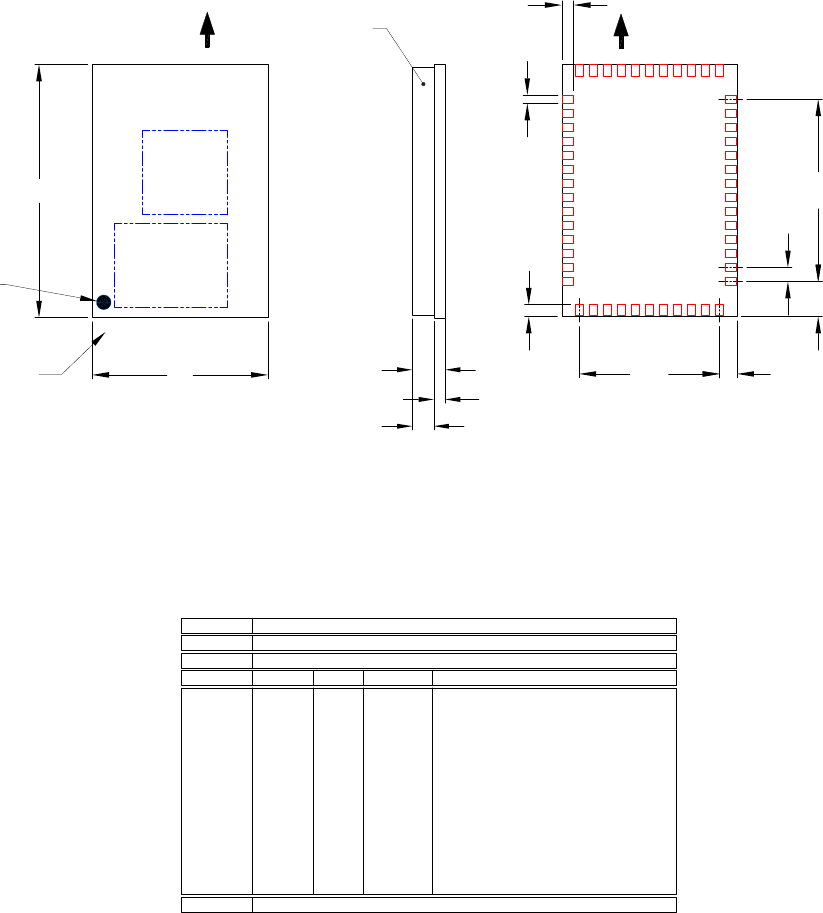
40
www.lairdtech.com
Laird Technologies
BTM410/411
Bluetooth® AT Data Module
MECHANICAL DETAILS
1
TOP VIEW
(COMPONENT SIDE)
E
D
RF OUT
Pin Outs
11
50
37
36
25
26
12
29
U1
U2
Orientation mark
on RF Shield
denotes pin 1
SIDE VIEW
A1
A2
A
RF Shield
BOTTOM VIEW
(SMT PADS)
29
RF OUT
D1
E1
e
G
H
b
11 1
50
12
37
25
26 36
H
F
Description 50 pin BT Data Module
Size18.0 x 12.5 x 2.5mm
Pitch 1mm
Dimension Minimum Typical Maximum Notes
A2.42.7
A1 0.80.91.0
A2 1.51.7
b 0.60
D12.37 12.5 12.63
E 17.87 18.0 19.13
e1.0
D1 10.0
E1 12.0
F1.25
G2.50
PCB Thickness
RF Shield Height
Global pad width
Global pitch
2.3
H0.85 Global length of pad to edge of board
Units mm
0.650.55
1.3
Pad Centre to Board edge
Pad Centre to Board edge
MECHANICAL
DRAWINGS
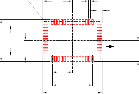
41
www.lairdtech.com
Laird Technologies
BTM410/411
Bluetooth® AT Data Module
RECOMMENDED PCB FOOTPRINT
1
11
12 25
26
37
36
50
19.2
1x13
6.5
pin pitch
6.85
29
RF OUT (See Note 1)
Pad Width 0.7 Typ
Pad Length 1.65 Typ
9.6
13.7
1x10
pin pitch
5
MODULE OUTLINE
(See note 2)
NOTES FOR PCB LAYOUT:
1. The RF output pin must be matched to a 50Ω strip-line or coplanar waveguide on the
antenna-less version (BTM410).
2. Ensure that there are no exposed conductors under the module to avoid shorts to the
test points on the module underside.
3. The pcb footprint is provided for guidance only. Users may wish to modify the PCB land
dimensions to suit their specic manufacturing or process.
MECHANICAL
DRAWINGS
42
www.lairdtech.com
Laird Technologies
BTM410/411
Bluetooth® AT Data Module
5
5
4
4
3
3
2
2
1
1
D D
C C
BB
AA
BTDMD-R-001-01 01
Mini Dev Board - Comms
C
1 2Friday, October 10, 2008
Title
Size Document Number Rev
Date: Sheet of
USB_DSR
USB_DCD
USB_CTS
PIO_3/DCD
Module_TX USB_RX
SPI_CLK_PC
SPI_CS_PC
SPI_MISO_PC
SPI_MOSI_PC
PCM_IN
PCM_CLK
PCM_SYNC
Module_RTS
Module_TX
RESET_ Module_RX
Module_CTS
PIO_2/RI
PIO_3/DCD
PIO_2/RI USB_PIO_2/RI
PIO_10/DSR
PIO_9/DTR
Module_RTS
Module_CTS
Module_RTS
SPI_MOSI
ANT
PIO_7
USB_MOD_D+
PIO_6
USB_MOD_D-
SPI_MISO
SPI_CS
PIO_9/DTR
PIO_2/RI
SPI_CLK
Module_RX
Module_TX
SPI_CLK_PC
SPI_CS_PC
SPI_CS
SPI_CLK
SPI_MOSI_PC
SPI_MOSI
SPI_MISO_PC
SPI_MISO
USB_MOD_D+ USB_MOD_D-
USB_TX Module_RX
Module_CTS
USB_RTS
USB_DTR
FTDI_EN
FTDI_EN
FTDI_EN
FTDI_EN
USB_PWREN
PCM_OUT
PIO_10/DSR
PIO_9/DTR
PIO_10/DSR
PIO_2/RI
PIO_3/DCD
PIO_9/DTR
PIO_10/DSR
PIO_4
PIO_4
PIO_5 PIO_7
PIO_6
PIO_5
PIO_3/DCD
PCM_IN
RESET_
PCM_CLK
PCM_OUT
PCM_SYNC
PCM_CLK
PCM_IN
PCM_OUT
PCM_SYNC
VCC_IO
VCC_3V3 VCC_3V3
VCC_3V3
VCC_IO VCC_IO
VCC_3V3
VCC_IO
VCC_3V3
VCC_3V3
VCC_IO
VCC_IO VCC_IO
VCC_3V3
VCC_3V3
VCC_3V3
VCC_3V3
VCC_3V3
VCC_3V3
VCC_3V3
VCC_3V3
VCC_3V3
VDD_CONN
VCC_3V3
VCC_IO
VCC_IO
VCC_IO
VCC_IO
VCC_IO
VCC_3V3
VCC_IO
VCC_IO
VDD_CONN VCC_3V3
R51
10K
12
R41
10K
12
U1
NC7SZ125
1
2
3
4
5
OE_
IN
GND
OUT
VCC
R13
10K
12
R47
10K
12
SW1
NF
1 3
2 4
R54
0R
1 2
R65
10K
12
R66 0R
12
R63
10K
1 2
R40
10K
1 2
R57
10K
1 2
R68
0R
12
C15
100n
12
R50
10K
1 2
C21
100n
12
R43
10K
12
R55
10K
12
J1
RJ45_Mod_Jack
1
2
3
4
5
6
7
8
1
2
3
4
5
6
7
8
U2
NC7SZ125
1
2
3
4
5
OE_
IN
GND
OUT
VCC
SW3
NF
13
2 4
R46
10K
1 2
R100
1K5
12
SW2
NF
13
24
R62
10K
12
TP5
1
R67
0R
12
JP3
NF
1
3
56
4
2
R60
10K
1 2
SW4
NF
1 3
2 4
R52
10K
12
C19
100n
12
R59
10K
1 2
C17
100n
12
U3
NC7SZ125
1
2
3
4
5
OE_
IN
GND
OUT
VCC
R3
10K
12
R45
0R
12
R42
10K
12
JP2
NF
1
3
5 6
4
2
JP1
NF Header 6X2
1 2
3 4
5 6
78
910
11 12
C18
100n
12
C16
100n
12
R58
10K
1 2
U5
NF 74LCX244
1
2
3
4
5
6
7
8
9
10 11
12
13
14
15
16
17
18
19
20
OE1_
I0
O4
I1
O5
I2
O6
I3
O7
GND I7
O3
I6
O2
I5
O1
I4
O0
OE2_
VCC
R44
10K
12
U4
BT_Data
1
2
3
4
5
6
10
11
12
14
15
16
17
18
7
8
21
22
23
24
25
26
27
28
40
39
38
37
36
34
35
33
32
31
30
29
9
13
19
20
41
42
43
44
45
46
47
48
49
50
N/C
GND
UART_CTS
UART_RX
UART_RTS
UART_TX
SPI_MOSI
SPI_CLK
VDD_USB
MASTER_VIN
GND
PCM_IN
PCM_SYNC
PCM_CLK
GND
SPI_CSB
GPIO6
PIO3/UART_DCD
GND
N/C
N/C
N/C
N/C
GND
N/C
N/C
N/C
N/C
N/C
N/C
N/C
N/C
N/C
N/C
GND
ANT
SPI_MISO
VDD_IO
PCM_OUT
RESET
GND
PIO2/UART_RI
PIO9/UART_DTR
PIO10/UART_DSR
GND
USB_D+/ RESERVED
USB_D-/ RESERVED
GPIO8
GPIO7
GPIO5
R49
0R
1 2
R64
10K
12
R18
10K
12
R8
10K
12
R61
10K
1 2
R56
10K
1 2
J5
HEADER 10 X 1
1
2
3
4
5
6
7
8
9
10
C20
100n
12
R48 0R
1 2
R53
10K
12
TP6
1
MECHANICAL
DRAWINGS
43
www.lairdtech.com
Laird Technologies
BTM410/411
Bluetooth® AT Data Module
5
5
4
4
3
3
2
2
1
1
D D
C C
BB
AA
BTDMD-R-001-01 01
Mini_Dev_Power_Supplies
C
2 2Friday, October 10, 2008
Title
Size Document Number Rev
Date: Sheet of
D-
50ohm Track 50_ohm Track
D+
USB-
USB+
USB_PWREN
USB_SLEEP
USB_RTS
USB_CTS
USB_RX
USB_TX
USB-
USB+
USB_PWREN
RESET_FTDI
USB_DTR
USB_DSR
USB_DCD
USB_PIO_2/RI
RESET_
ANT
USB_MOD_D+
USB_MOD_D-
VDD_3V3_IO
VDD_USB
VDD_3V3_IO
VDD_CONN
VDD_USB
VCC_3V3
VCC_3V3
VCC_3V3
VDD_USB
VCC_3V3
VCC_3V3
VDD_CONN
R85 N/F
12
C30
1n
12
TP8
1
R79
10K
1 2
M3
Mounting Hole
C25
10N
12
TP13
R77
1K
1 2
R80
1K
1 2
R86
10K
1 2
R82 0R
1 2
J6
SMA_Vert
1
2
3
4
5
C23
100n
12
L5
BLM18PG221SN1D
1 2
C28
NF
12
M4
Mounting Hole
R91
NF 9K1
12
TP15
TP14
TP11
TH_TEST_POINT
1
C24
100n
12
TP12
TH_TEST_POINT
1
R74
0.1R 0805
12
JP5
-
USB B
1
2
3
4
56
Vcc
D-
D+
GND
56
D6
BAT54C
1
2
3
R75 10K
12
R72
9K1
12
R84
10K
1 2
FID1
Fiducial
R92
NF 9K1
12
D3
Diode_S1A
1 2
C27
100n
12
Q1 IRF5810
1
56
42
3
FID2
Fiducial
D5
HSMG-A100-HO1J1
21
R81 0R
12
R93 NF 0R
1 2
U6
MCP1726-ADJE/MF
1
2
3
45
6
7
8
9
Vin_1
Vin_2
/SHDN
GND PWRGD
Cdelay
ADJ
Vout
GND
R76
1K3
12
C29
100n
12
R73
110R
12
C26
2u2
12
M1
Mounting Hole
R11
NF 9K1
12
C22
2u2
12
U7
NC7SV17
1
2
3
4
5
NC1
IN
GND
OUT
VCC
R88
4K7
12
TP7
1
CN1
DC Power jack_2.1mm
1
2
3
R90
0R
1 2
U8
FT232R
30
31
32
1
2
3
4
6
7
8
11
10
28
27
26
24
21
9
20 19
18
17
16
15
14
5
12
13
22
23
25
29
33
TXD
DTR#
RTS#
VCCIO
RXD
RI#
GND
DSR#
DCD#
CTS#
CBUS3
CBUS2
OSCO
OSCI
TEST
AGND
CBUS1
CBUS4
GND VCC
RESET#
GND
3V3OUT
USBDM
USBDP
NC_5
NC_4
NC_6
CBUS0
NC_1
NC_2
NC_3
THPAD
R94 NF 0R
1 2
R83
4.7K
12
M2
Mounting Hole
SW6
BFS-1000
13
2 4
R87
10K
12
R78
10K
12
OFF
SW5
3 position switch
2
1
3
C31
100n
12
MECHANICAL
DRAWINGS

44
BTM410/411
Bluetooth® AT Data Module
global solutions:
local support
TM
USA: +1.800.492.2320
Europe: +44.1628.858.940
Asia: +852.2268.6567
wirelessinfo@lairdtech.com
www.lairdtech.com/wireless
ORDERING INFORMATION
GENERAL COMMENTS
This is a preliminary datasheet. Please check with Laird Technologies for the latest information before
commencing a design. If in doubt, ask.
Refer to the schematic BTDMD-R-001.pdf for the Development Kit on the following two pages for examples
of typical pin connections. A pdf of the schematic can be downloaded from the product web page.
PART NUMBER DESCRIPTION
BTM410 Bluetooth AT Data Module (external antenna)
BTM411 Bluetooth AT Data Module (with integrated antenna) Q1-2009
DVK – BTM410 Development board with BTM410 module soldered in place
DVK – BTM411 Development board with BTM411 module soldered in place Q2-2009
ORDERING
INFORMATION

45
Laird Technologies is the world leader in the design and
manufacture of customized, performance-critical products for
wireless and other advanced electronics applications.
Laird Technologies partners with its customers to nd
solutions for applications in various industries such as:
Network Equipment
Telecommunications
Data Communications
Automotive Electronics
Computers
Aerospace
Military
Medical Equipment
Consumer Electronics
Laird Technologies offers its customers unique
product solutions, dedication to research and
development, as well as a seamless network of
manufacturing and customer support
facilities across the globe.
LWS-UM-BTM410-411 0409
Copyright © 2009 Laid Technologies, Inc. All rights reserved.
The information contained in this manual and the accompanying software programs are copyrighted and all rights are reserved by Laird Technologies, Inc. Laird Technologies, Inc. reserves the right to make periodic
modications of this product without obligation to notify any person or entity of such revision. Copying, duplicating, selling, or otherwise distributing any part of this product or accompanying documentation/software
without the prior consent of an authorized representative of Laird Technologies,Inc. is strictly prohibited.
All brands and product names in this publication are registered trademarks or trademarks of their respective holders.
This material is preliminary
Information furnished by Laird Technologies in this specication is believed to be accurate. Devices sold by Laird Technologies are covered by the warranty and patent indemnication provisions appearing in its Terms
of Sale only. Laird Technologies makes no warranty, express, statutory, and implied or by description, regarding the information set forth herein. Laird Technologies reserves the right to change specications at any
time and without notice. Laird Technologies’ products are intended for use in normal commercial and industrial applications. Applications requiring unusual environmental requirements such as military, medical life-
support or life-sustaining equipment are specically not recommended without additional testing for such application.
Limited Warranty, Disclaimer, Limitation of Liability
For a period of one (1) year from the date of purchase by the OEM customer, Laird Technologies warrants the OEM transceiver against defects in materials and workmanship. Laird Technologies will not honor this
warranty (and this warranty will be automatically void) if there has been any (1) tampering, signs of tampering; 2) repair or attempt to repair by anyone other than an Laird Technologies authorized technician. This
warranty does not cover and Laird Technologies will not be liable for, any damage or failure caused by misuse, abuse, acts of God, accidents, electrical irregularity, or other causes beyond Laird Technologies’ control,
or claim by other than the original purchaser. In no event shall Laird Technologies be responsible or liable for any damages arising: From the use of product; From the loss of use, revenue or prot of the product; or
As a result of any event, circumstance, action, or abuse beyond the control of Laird Technologies, whether such damages be direct, indirect, consequential, special or otherwise and whether such damages are incurred
by the person to whom this warranty extends or third party. If, after inspection, Laird Technologies’ determines that there is a defect, Laird Technologies will repair or replace the OEM transceiver at their discretion. If
the product is replaced, it may be a new or refurbished product.