Fairchild An 7511 Users Manual Insulated Gate Transistors Simplify AC Motor Speed Control
AN-7511 to the manual 016f8c97-e41d-4a13-adba-4af83a5d97e4
2015-02-09
: Fairchild Fairchild-An-7511-Users-Manual-550597 fairchild-an-7511-users-manual-550597 fairchild pdf
Open the PDF directly: View PDF ![]() .
.
Page Count: 13
©2002 Fairchild Semiconductor Corporation Application Note 7511 Rev. A1
Insulated-Gate Transistors Simplify AC-Motor
Speed Control
An IGT’s few input requirements and low On-state resistance
simplify drive circuitry and increase power efficiency in motor-
control applications. The voltage-controlled, MOSFET-like
input and transfer characteristics of the insulated-gate transis-
tor (IGT) (see EDN, September 29, 1983, pg 153 for IGT
details) simplify power-control circuitry when compared with
bipolar devices. Moreover, the IGT has an input capacitance
mirroring that of a MOSFET that has only one-third the power-
handling capability. These attributes allow you to design sim-
ple, low-power gate-drive circuits using isolated or level-shift-
ing techniques. What’s more, the drive circuit can control the
IGT’s switching times to suppress EMI, reduce oscillation and
noise, and eliminate the need for snubber networks.
Use Optoisolation To Avoid Ground Loops
The gate-drive techniques described in the following sections
illustrate the economy and flexibility the IGT brings to power
control: economy, because you can drive the device’s gate
directly from a preceding collector, via a resistor network, for
example; flexibility, because you can choose the drive circuit’s
impedance to yield a desired turn-off time, or you can use a
switchable impedance that causes the IGT to act as a charge-
controlled device requiring less than 10 nanocoulombs of
drive charge for full turn-on.
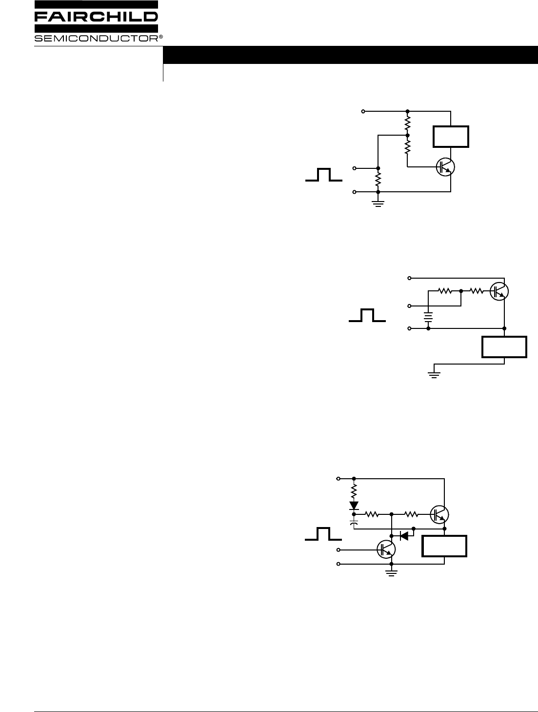
Take Some Driving Lessons
Note the IGT’s straightforward drive compatibility with CMOS,
NMOS and open-collector TTL/HTL logic circuits in the
common-emitter configuration Figure 1A. R3 controls the turn-
off time, and the sum of R3 and the parallel combination of R1
and R2 sets the turn-on time. Drive-circuit requirements,
however, are more complex in the common-collector
configuration Figure 1B.
In this floating-gate-supply floating-control drive scheme, R1
controls the gate supply’s power loss, R2 governs the turn-off
time, and the sum of R1 and R2 sets the turn-on time. Figure
1C shows another common-collector configuration employing
a bootstrapped gate supply. In this configuration, R3 defines
the turn-off time, while the sum of R2 and R3 controls the turn-
on time. Note that the gate’s very low leakage allows the use
of low-consumption bootstrap supplies using very low-value
capacitors. Figure 1 shows two of an IGT’s strong points. In
the common-emitter Figure 1A, TTL or MOS-logic circuits can
drive the device directly. In the common-collector mode, you’ll
need level shifting, using either a second power supply Figure
1B or a bootstrapping scheme Figure 1C.
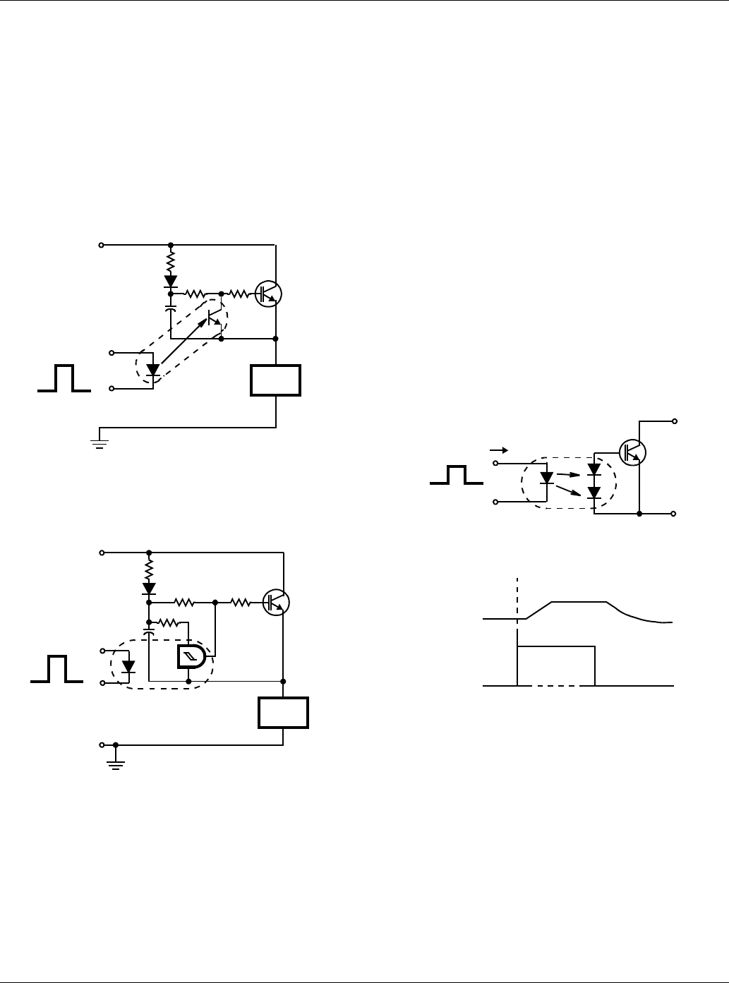
In the common-collector circuits, power-switch current flowing
through the logic circuit’s ground can create problems.
Optoisolation can solve this problem (Figure 2A.) Because of
the high common-mode dV/dt possible in this configuration,
you should use an optoisolator with very low isolation capaci-
tance; the H11AV specs 0.5pF maximum.
FIGURE 1A.SIMPLE DRIVING AND TRANSITION-TIME
CONTROL
FIGURE 1B. A SECOND POWER SUPPLY
FIGURE 1C. BOOTSTRAPPING SCHEME
LOAD
VCC
R1
R3
R2
ON
OFF 15 VCCR2
R1R2
+
--------------------25V
≤≤
R3 CONTROLS tOFF
LOAD
VCC
CONTROL
INPUT
ON
OFF 15V
R1R2
R1 CONTROLS GATE
SUPPLY POWER LOSS
R2 CONTROLS tOFF
R1 + R2 CONTROLS tON
LOAD
ON
OFF
15 VCCR2
R1R2
+
--------------------25V
≤≤
R3 CONTROLS tOFF
R2 + R3 CONTROLS tO
N
τ5C
ICEO IGES 2IR
++
-------------------------------------------------«
R1
R3
R2
Application Note September 1993 AN-7511
/T
itle
AN
75
1)
Su
b-
ect
In
ula
ted
Ga
te
ra
n
ist
ors
im
-
lif
y
C
-
o
tor
pe
ed
on
-
rol
)
Au
tho
()
Ke
y-
or
ds
Int
er-
il
or
po-
ati
on,
em
i-
on
-
uc
tor,
va
-
anc
he
ne
rgy
at
ed,
w
itch
ng
ow
er
up
-
lie
,
ow
er
©2002 Fairchild Semiconductor Corporation Application Note 7511 Rev. A1
For optically isolated “relay-action” switching, it makes sense
to replace the phototransistor optocoupler with an H11L1
Schmitt-trigger optocoupler (Figure 2B).) For applications
requiring extremely high isolation, you can use an optical fiber
to provide the signal to the gate-control photodetector. These
circuit examples use a gate-discharge resistor to control the
IGT’s turn-off time. To exploit fully the IGT’s safe operating
area (SOA), this resistor allows time for the device’s minority
carriers to recombine. Furthermore, the recombination occurs
without any current crowding that could cause hot-spot forma-
tion or latch-up pnpn action. For very fast turn-off, you can use
a minimal snubber network, which allows the safe use of lower
value gate resistors and higher collector currents.
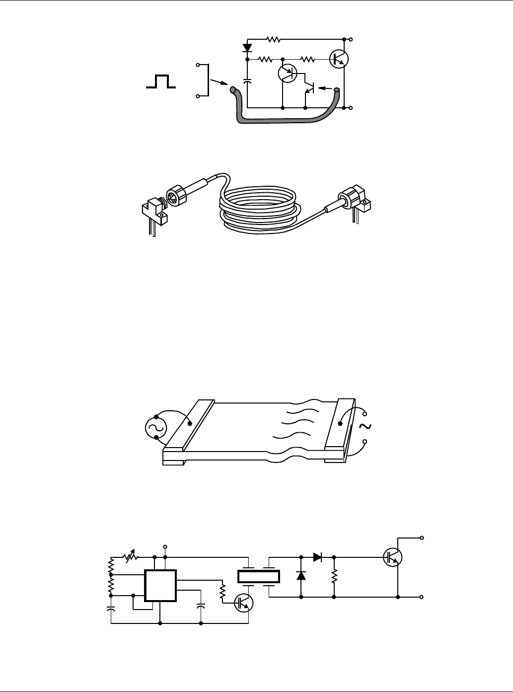
Pulse-Transformer Drive Is Cheap And Efficient
Photovoltaic couplers provide yet another means of driving the
IGT. Typically, these devices contain an array of small silicon
photovoltaic cells, illuminated by an infrared diode through a
transparent dielectric. The photovoltaic coupler provides an
isolated, controlled, remote dc supply without the need for
oscillators, rectifiers or filters. What’s more, you can drive it
directly from TTL levels, thanks to its 1.2V, 20mA input
parameters.
Available photovoltaic couplers have an output-current
capability of approximately 100µA. Combined with
approximately 100kΩ equivalent shunt impedance and the
IGT’s input capacitance, this current level yields very long
switching times. These transition times (typically ranging to 1
msec) vary with the photovoltaic coupler’s drive current and the
IGT’s Miller-effect equivalent capacitance.
Figure 3 illustrates a typical photovoltaic-coupler drive along
with its transient response. In some applications, the
photovoltaic element can charge a storage capacitor that’s
subsequently switched with a phototransistor isolator. This
isolator technique - similar to that used in bootstrap circuits
provides rapid turn-on and turn-off while maintaining small size,
good isolation and low cost.
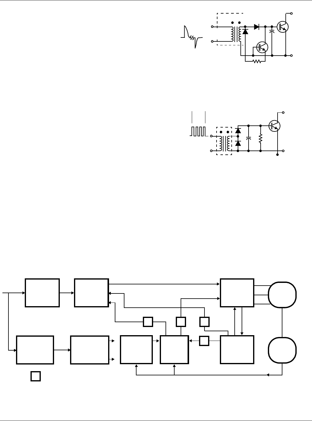
In common-collector applications involving high-voltage, reac-
tive-load switching, capacitive currents in the low-level logic cir-
cuits can flow through the isolation capacitance of the control
element (eg, a pulse transformer, optoisolator, piezoelectric
coupler or level-shift transistor). These currents can cause
undesirable effects in the logic circuitry, especially in high-
impedance, low-signal-level CMOS circuits.
FIGURE 3. AS ANOTHER OPTICAL-DRIVE OPTION, A PHOTO-
VOLTAIC COUPLER PROVIDES AN ISOLATED,
REMOTE DC SUPPIY TO THE IGT’S INPUT. ITS
LOW 100µA OUTPUT, HOWEVER, YIELDS LONG
IGT TURN-ON AND TURN-OFF TIMES.
The solution? Use fiber-optic components Figure 4 to elimi-
nate the problems completely. As an added feature, this low-
cost technique provides physical separation between the
power and logic circuitry, thereby eliminating the effects of
radiated EMI and high-flux magnetic fields typically found
near power-switching circuits. You could use this method
with a bootstrap-supply circuit, although the fiber-optic sys-
tem’s reduced transmission efficiency could require a
gain/speed trade-off. The added bipolar signal transistor
minimizes the potential for compromise.
FIGURE 2A. AVOID GROUND-LOOP PROBLEMS BY USING AN
OPTOISOLATOR. THE ISOLATOR IGNORES SYS-
TEM GROUND CURRENTS AND ALSO PRO-
VIDES HIGH COMMON-MODE RANGE.
FIGURE 2B. A SCHMITT-TRIGGER OPTOISOLATOR YIELDS
“SNAP-ACTION” TRIGGERING SIMILAR TO
THAT OF A RELAY.
LOAD
VCC
R1
R2R3
CONTROL
INPUT
C
OFF
ON
H11AV2
LOAD
VCC = 300V
43k
1N5061
5.6k
10µF
35V
CONTROL
INPUT
OFF
ON
H11L1
5.6k 5.6k
DIG22 IGT
ON
OFF
CONTROL
INPUT
+
-
I
OUTPUT
CURRENT
INPUT
CURRENT 012ms
Application Note 7511
©2002 Fairchild Semiconductor Corporation Application Note 7511 Rev. A1
FIGURE 5A. YIELDING 4-kV ISOLATION, A PIEZOELECTRIC COUPLER PROVIDES TRANSFORMER-LIKE PERFORMANCE AND AN
ISOLATED POWER SUPPLY.
FIGURE 5B. THIS CIRCUIT PROVIDES THE DRIVE FOR THIS ARTICLE’S MOTOR-CONTROL CIRCUIT.
CONTROL
INPUT
ON
OFF
GFOE1A1
EMITTER
(DISCONNECTED) DETECTOR
(CONNECTED
)
10M (30FT)
QSF2000C
(W/CONNECTORS)
GFOD1A1
1N914
R1
2N5354
CQ1
R2R3
IGT
+
-
FIGURE 4. ELIMINATE EMI IN HIGH-FLUX OR NOISE ENVI-
RONMENTS BY USING FIBER-OPTIC COMPO
-
NENTS. THESE PARTS ALSO ALLEVIAT
E
PROBLEMS ARISING FROM CAPACITIVE COU
-
PLING IN ISOLATION ELEMENTS.
P
iezos Pare Prices
OUTPUT
VOLTAGE
ACOUSTIC WAVE
OSCILLATOR
IGT
4.7k
1N914
1N914
PZ61343
D33D21
18V
2.5k
3.3k
2.7k
0.001
µF
0.001
µF
1k
NE555
Application Note 7511
©2002 Fairchild Semiconductor Corporation Application Note 7511 Rev. A1
A piezoelectric coupler operationally similar to a pulse-train
drive transformer, but potentially less costly in high volume is
a small, efficient device with isolation capability ranging to
4kV. What’s more, unlike optocouplers, they require no
auxiliary power supply. The piezo element is a ceramic
component in which electrical energy is converted to
mechanical energy, transmitted as an acoustic wave, and
then reconverted to electrical energy at the output terminals
Figure 5A.
The piezo element’s maximum coupling efficiency occurs at
its resonant frequency, so the control oscillator must operate
at that frequency. For example, the PZT61343 piezo coupler
in Figure 5B’s driver circuit requires a 108kHz, ±1%-accurate
astable multivibrator to maximize mechanical oscillations in
the ceramic material. This piezo element has a 1W max
power handling capability and a 30mA p-p max secondary
current rating. The 555 timer shown provides compatible
waveforms while the RC network sets the frequency.
Isolate With Galvanic Impunity
Do you require tried and true isolation? Then use
transformers; the IGT’s low gate requirements simplify the
design of independent, transformer-coupled gate-drive
supplies. The supplies can directly drive the gate and its
discharge resistor Figure 6, or they can simply replace the
level-shifting supplies of Figure 2. It’s good practice to use
pulse transformers in drive circuitry, both for IGT’s and
MOSFETs, because these components are economical,
rugged and highly reliable.
FIGURE 6A. PROVIDING HIGH ISOLATION AT LOW COST, PULSE
TRANSFORMERS ARE IDEAL FOR DRIVING THE
IGT. AT SUFFICIENTLY HIGH FREQUENCIES, C1
CAN BE THE IGT’S GATE-EMITTER CAPACITANCE
ALONE.
FIGURE 6B. A HIGH-FREQUENCY OSCILLATOR IN THE TRANS-
FORMER’S PRIMARY YIELDS UNLIMITED ON-
TIME CAPABILITY.
In the pulse-on, pulse-off method Figure 6A, C1 stores a
positive pulse, holding the IGT on. At moderate frequencies
(several hundred Hertz and above), the gate-emitter
capacitance alone can store enough energy to keep the IGT
on; lower frequencies require an additional external capacitor.
Use of the common-base n-p-n bipolar transistor to discharge
the capacitance minimizes circuit loading on the capacitor.
This action extends continuous on-time capability without
capacitor refreshing; it also controls the gate-discharge time
via the 1kΩ emitter resistor.
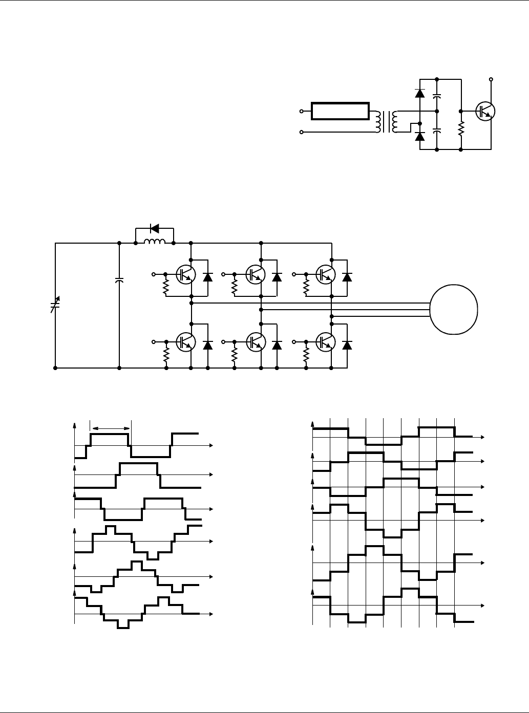
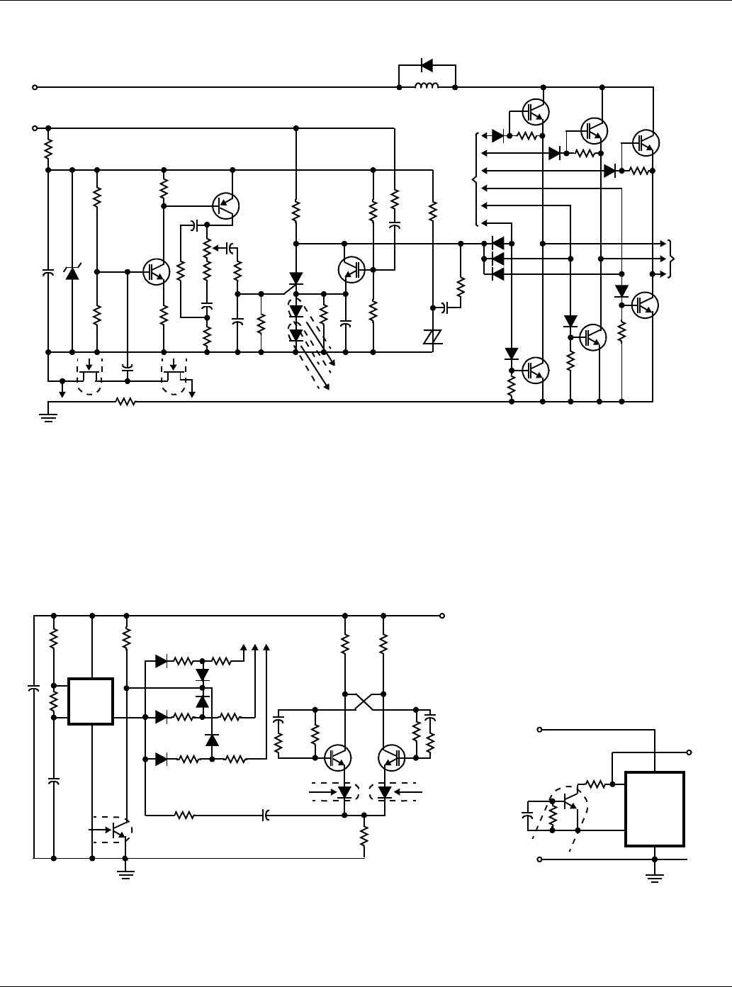
FIGURE 8. THIS 6-STEP 3-PHASE-MOTOR DRIVE USES THE IGT-DRIVE TECHNIQUES DESCRIBED IN THE TEXT. THE REGULATOR AD-
JUSTS THE OUTPUT DEVICES’ INPUT LEVELS; THE VOLTAGE-CONTROLLED OSCILLATOR VARIES THE SWITCHING
FREQUENCY AND ALSO PROVIDES THE CLOCK FOR THE 3-PHASE TIMING LOGIC. THE V/F RATIO STAYS CONSTANT
TO MAINTAIN CONSTANT TORQUE REGARDLESS OF SPEED.
ON
OFF
CONTROL
INPUT 1N914
1N914
2N5232
PULSE
TRANSFORMER
1k
C1IGT
+
-
IGT
+
-
ON OFF 1N914
CONTROL
INPUT
1N914 RC = 3µSEC
CR
CURRENT
SENSE
SIGNAL
ENABLE
LOWER
LEGS
SHUT DOWN
DRIVE
OSCILLATOR
VARIABLE
DC VOLTAGE
TIMING
AND DRIVE
VOLTAGE
ENABLE
ADJUST VOLTAGE
5V
24V
24V DC
220V AC
3φ 60Hz THREE-PHASE
BRIDGE
RECTIFIER
LOW VOLTAGE
TRANSFORMER
RECTIFIER
FILTER
SWITCHING
REGULATOR
POWER SUPPLY
FOR CONTROL
CIRCUITS
VOLTAGE
CONTROLLED
OSCILATOR
MOTOR
CONTROL
LOGIC
OVERLOAD
PROTECTION
THREE-PHASE
IGT
INVERTER
TACHO-
METER
FEEDBACK
SIGNAL PATH ISOLATOR
EG: OPTOCOUPLIER PIEZO COUPLER
3φ
INDUCTION
MOTOR
III
I
I
Application Note 7511
©2002 Fairchild Semiconductor Corporation Application Note 7511 Rev. A1
Piezoelectric Couplers Provide 4-kV Isolation
Using a high-frequency oscillator for pulse-train drive Figure
6B yields unlimited on-time capability. However, the scheme
requires an oscillator that can be turned on and off by the
control logic. A diode or zener clamp across the trans-
former’s primary will limit leakage-inductance flyback effects.
To optimize transformer efficiency, make the pulses’ voltage
x time products equal for both the On and the Off pulses. In
situations where the line voltage generates the drive power,
a simple relaxation oscillator using a programmable unijunc-
tion transistor can derive its power directly from the line to
provide a pulse train to the IGT gate.
The circuit shown in Figure 7 accommodates applications
involving lower frequencies (a few hundred Hertz and
below). The high oscillator frequency (greater than 20kHz)
helps keep the pulse transformer reasonably small. The volt-
age-doubler circuitry improves the turn-on time and also pro-
vides long on-time capability. Although this design uses only
a 5V supply on the primary side of a standard trigger trans-
former, it provides 15V gate-to-emitter voltage.
FIGURE 7. THIS DRIVING METHOD FOR LOW-FREQUENCY
SWITCHING PROVIDES 15V TO THE IGT’S GATE
OSCILLATOR 1:2
1N914
0.001µF
4.7k
0.001
µFIGT
1N914
FIGURE 9A. THE POWER INVERTER’S DRIVE CIRCUIT USES SIX IGTS TO DRIVE A 2-HP MOTOR.
FIGURE 9B. THE TIMING DIAGRAM SHOWS THAT EACH IGT
CONDUCTS FOR 165o× OF EVERY 360o CYCLE;
THE DELAY IS NECESSARY TO AVOID CROSS
CONDUCTION.
FIGURE 9C. THE THREE WINDINGS’ VOLTAGES AND CUR-
RENTS ARE SHOWN. NOTE THAT ALTHOUGH
COSTLY SNUBBER NETWORKS ARE ELIMINAT-
ED, FREEWHEELING DIODES ARE NEEDED; THE
IGTS HAVE NO INTRINSIC OUTPUT DIODE.
INDUCTION
MOTOR
D
7
325V
10A
NOTES:
Q1 - Q6 = D94FR4
D1 - D7 = 1N3913
D8 - D13 = 1N914
R = 4.7k, 1/2W
C1 = 100µF, 400V
L1 = 40µH
220V
L1
D1
D2
Q2
Q1
R
R
C1
D3D5
Q3Q5
RR
RR Q4Q6
D4D6
t
t
t
t
t
t0
0
0
0
0
0
φA
φB
φC
ILA
ILB
ILC
Q1 ON
Q2ON
Q3ON
180o
15o DELAY
Q4ON
Q5ON
Q6ON
VAB
0t
VBC
VCA
ILA
ILB
ILC
0
0
0
0
0
t
t
t
t
t
Application Note 7511
©2002 Fairchild Semiconductor Corporation Application Note 7511 Rev. A1
Polyphase motors, controlled by solid-state, adjustable-fre-
quency ac drives, are used extensively in pumps, conveyors,
mills, machine tools and robotics applications. The specific con-
trol method could be either 6-step or pulse-width modulation.
This section describes a 6-step drive that uses some of the pre-
viously discussed drive techniques (see page 11, “Latch-Up:
Hints, Kinks and Caveats”).
Figure 8 defines the drive’s block diagram. A 3-phase rectifier
converts the 220V ac to dc; the switching regulator varies the
output voltage to the IGT inverter. At the regulator’s output, a
large filter capacitor provides a stiff voltage supply to the
inverter.
The motor used in this example has a low slip characteristic
and is therefore very efficient. You can change the motor’s
speed by varying the inverter’s frequency. As the frequency
increases, however, the motor’s air-gap flux diminishes, reduc-
ing developed-torque capability. You can maintain the flux at a
constant level (as in a dc shunt motor) if you also vary the volt-
age so the V/F ratio remains constant.
Fiber-Optic Drive Eliminates Interference
In the example given, the switching regulator varies the IGT
inverter’s output by controlling its dc input; the voltage-con-
trolled oscillator (VCO) adjusts the inverter’s switching fre-
quency, thereby varying the output frequency. The VCO also
drives the 3-phase logic that provides properly timed pulsed
outputs to the piezo couplers that directly drive the IGT.
Sensing the dc current in the negative rail and inhibiting the
gate signal protect the IGT from overload and shoot-through
(simultaneous conduction) conditions. If a fault continues to
exist for an appreciable period, inhibiting the switching regu-
lator causes the inverter to shut off. The inverter’s power-out-
put circuit is shown in Figure 9A; the corresponding timing
diagrams show resistive-load current waveforms that indi-
cate the 3-phase power Figure 9B and waveforms of the out-
put line voltage and current Figure 9C.
In Figure 9’s circuit, it appears that IGTs Q1 through Q6 will
conduct for 180o. However, in a practical situation, it’s neces-
sary to provide some time delay (typically 10o to 15o×) dur-
ing the positive-to-negative transition periods in the phase
current. This delay allows the complementary IGTs to turn
off before their opposite members turn on, thus preventing
cross conduction and eventual destruction of the IGTs.
Because of the time delay, the maximum conduction time is
165o of every 360o period. Because the IGTs don’t have an
integral diode, it’s necessary to connect an antiparallel diode
externally to allow the freewheeling current to flow. Inductor
L1 limits the di/dt during fault conditions; freewheeling diode
D7 clamps the IGT’s collector supply to the dc bus.
The peak full-load line current specified by the motor manu-
facturer determines the maximum steady-state current that
each transistor must switch. You must convert this RMS-
specified current to peak values to specify the proper IGT. If
the input voltage regulator had a fixed output voltage and a
constant frequency, each IGT would be required to supply
the starting locked-rotor current to the motor. This current
could be as much as 15 times the full-load running current.
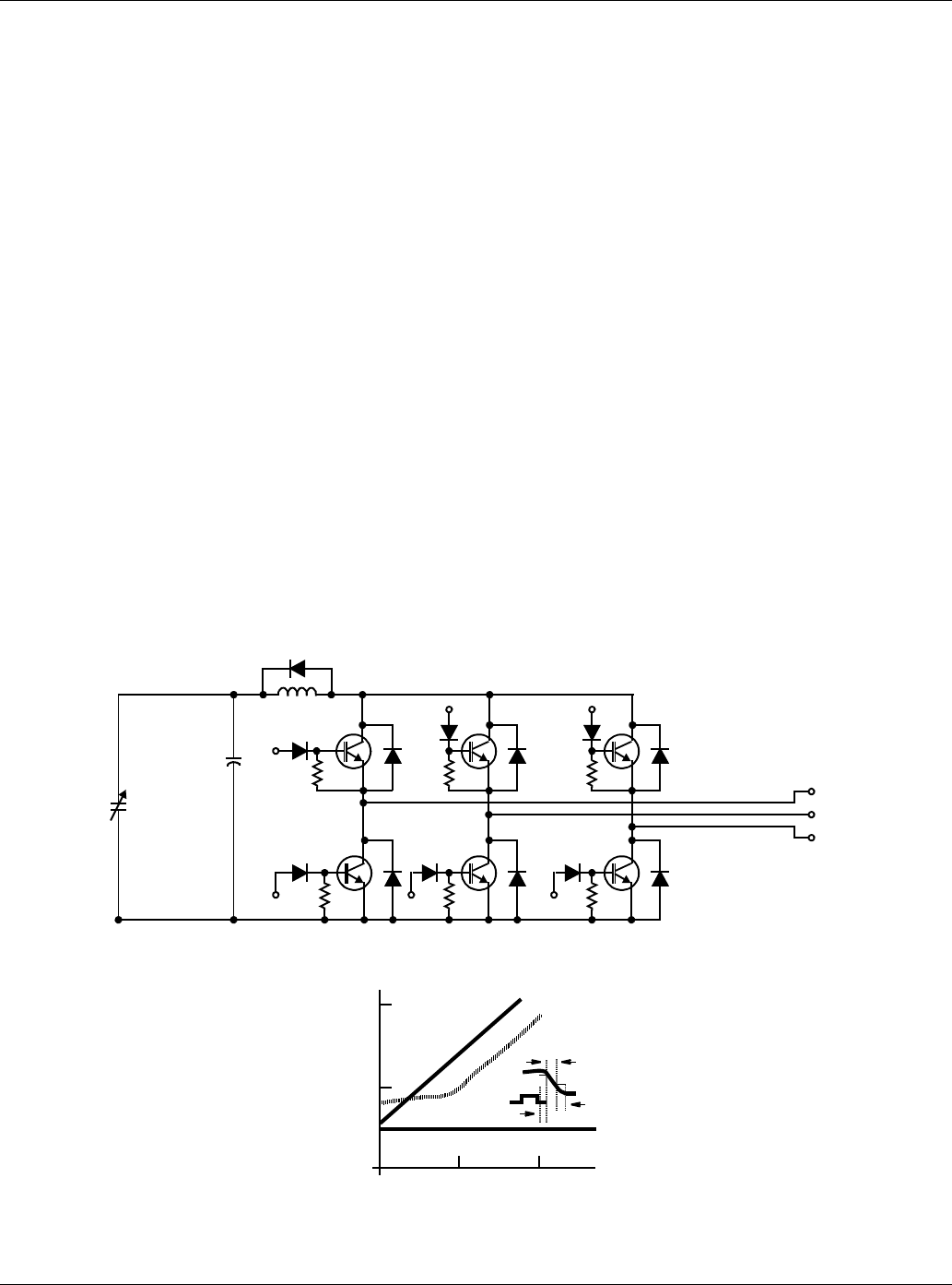
FIGURE 10A. COMPONENT SELECTION IS IMPORTANT. THE IGT SELECTED CIRCUIT HANDLES 10A, 500V AT 150oC. THE ANTI-
PARALLEL DIODES HAVE A SIMILAR CURRENT RATING.
FIGURE 10B. SELECT R TO YIELD THE DESIRED TURN-OFF TIME. FINALLY, L1’S VALUE DETERMINES THE FAULT-CONDITION
ACTION TIME.
D
7
0 TO 325V
10A
SWITCHES ON” (1, 4, 5),
(1, 3, 6), (2, 3, 6),
(2, 3, 5), (2, 4, 5)
L1
D1
Q1
R
C1D5
Q5
R
R
Q6D6
TO
LOAD
D13
D10
R
Q4D4
D9
R
Q2D2
D8
D3
Q3
R
D12
D11
+
10
1
0.1
100 1k 10k
RGE
tD(OFF) tF1
tF2 tF2
tF1
tD(OFF)
IC
0.9IC0.1IC
0
Application Note 7511
©2002 Fairchild Semiconductor Corporation Application Note 7511 Rev. A1
It’s impractical, however, to rate an inverter based on locked-
rotor current. You can avoid this necessity by adjusting the
switching regulator’s output voltage and by providing a fixed
output-current limit slightly higher than the maximum full-
load current. This way, the current requirements during start-
up will never exceed the current capability of an efficiently
sized inverter.
For example, consider a 2-hp, 3-phase induction motor spec-
ifying VL at 230V RMS and full-load current (ILFL) at 6.2A
RMS. For the peak current of 8.766A, you can select IGT
type D94FR4. This device has a reverse-breakdown SOA
(RBSOA) of 10A, 500V for a clamped inductive load at a
junction temperature of 150oC. A 400V IGT could also do the
job, but the 500V choice gives an additional derating safety
margin. You must set the current limit at 9A to limit the in-
rush current during start-up. Note that thanks to the IGT’s
adequate RBSOA, you don’t need turn-off snubbers.
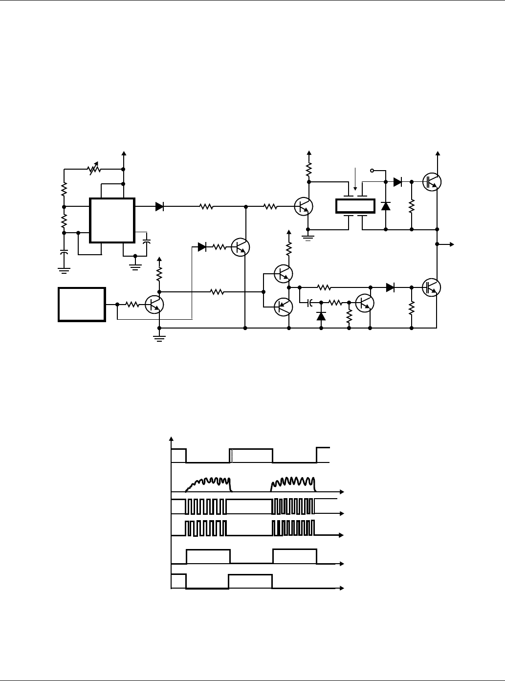
FIGURE 11A. PROVIDING PROPERLY TIMED DRIVE TO THE IGTS, THE CIRCUIT USES PIEZO COUPLING TO THE UPPER POWER
DEVICE. THE 3-TRANSISTOR DELAY CIRCUIT PROVIDES THE NEEDED 15o LAG TO THE LOWER IGT TO AVOID
CROSS CONDUCTION.
FIGURE 11B. THE TIMING DIAGRAM SHOWS THE 555’S 108-KHz DRIVE TO THE PIEZO DEVICE AND THE LATTER’S SLOW
RESPONSE.
1N914
NE555
4
783
21
56
2N3903
VCO &
TIMING
LOGIC
1000pF
2.7k
3.3k 1k
5V
0.001µF
5V
A4.7k
470
Q7
B
1N914 4.7k
C
Q8
2N3903
2N3903
Q8
470
470
1N914
1N914
2N3903
1N914
D33030
D29E10
1N914
D94FR4
D94FR4
PIEZOCOUPLER
24V
24V
Q3
Q4Q5
Q1
Q2
4.7k
4.7k
10
10
22µF
C1
DC BUS
φA
E
F
D
3
PZT61343
1k
470
2.5k
VOLTS
24V
F
24V
E
24V
D
C
B
A
TIME
TIME
TIME
TIME
TIME
5V
5V
5V
100kHz
Application Note 7511
©2002 Fairchild Semiconductor Corporation Application Note 7511 Rev. A1
Use 6-Step Drive For Speed-Invariant Torque
Figure 10A shows the inverter circuit configured for this
example. Diodes D1 through D6 carry the same peak current
as the IGTs; consequently, they’re rated to handle peak cur-
rents of at least 8.766A. However, they only conduct for a
short time (15o to 20o of 180o), so their average-current
requirement is relatively small.
External circuitry can control the IGT’s current fall time.
Resistor R controls tF1 Figure 10B; there's no way to control
tF2, an inherent characteristic of the selected IGT. In this
example, a 4.7-kΩ gate-to-emitter resistor provides the
appropriate fall time. The choice of current-limiting inductor
L1 is based on the IGT’s overload-current rating and the
action time (the sum of the sensor’s sensing and response
time and the IGT’s turn-off time) in fault conditions.
You could use a set of flip flops and a multivibrator to gener-
ate the necessary drive pulses and the corresponding 120o×
delay between the three phases in Figure 10’s circuit. A volt-
age-controlled oscillator serves to change the inverter’s out-
put frequency. In this circuit, IGTs Q1, Q3 and Q5 require
isolated gate drive; the drive for Q2, Q4 and Q6 can be
referred to common. If you use optocouplers for isolation,
you’ll need three isolated or bootstrap power supplies (in
addition to the 5V and 24V power supplies) to drive the IGTs.
Another alternative is to use transformer coupling.
165o Conduction Prevents Shoot-Through
Consider, however, using Figure 11A’s novel, low-cost cir-
cuit. It uses a piezo coupler to drive the isolated IGT. As
noted, the coupler needs a high-frequency square wave to
induce mechanical oscillations in its primary side. The 555
oscillator provides the necessary 108-kHz waveform; its out-
put is gated according to the required timing logic and then
applied to the piezo coupler’s primary. The coupler’s rectified
output drives the IGT’s gate; the 4.7kW gate-to-emitter resis-
tor provides a discharge path for CGE during the IGT’s turn-
off. The circuit’s logic-timing diagram is shown in Figure 11B.
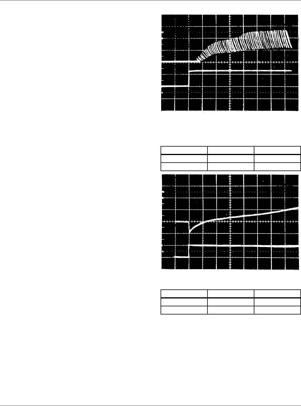
The piezo coupler’s slow response time Figure 12A contrib-
utes approximately 2o to the 15o to 20o turn-on/turn-off delay
needed to avoid shoot-through in the complementary pairs.
The corresponding collector current is shown in Figure 12B.
C1 and its associated circuitry provide the remaining delay
as follows:
FIGURE 12A. THE PIEZO COUPLER’S SLOW RESPONSE IS NOT
A DISADVANTAGE IN THIS ARTICLE’S CIRCUIT. IN
FACT, IT CONTRIBUTES 2o TO THE REQUIRED 15o
TURN-ON/TURN-OFF DELAY.
FIGURE 12B. THE DRIVEN IGT'S COLLECTOR CURRENT IS
SHOWN
When Q3’s base swings negative, C1 - at this time discharged -
turns on Q5. Once C1 is charged, Q5 turns off, allowing a drive
pulse to turn the IGT on. When Q7’s base goes to ground, Q4
turns on and discharges C1, initiating the IGT’s turn-off. Figure
13 shows the motor current and corresponding line voltage
under light-load Figure 12A and full-load Figure 12B conditions.
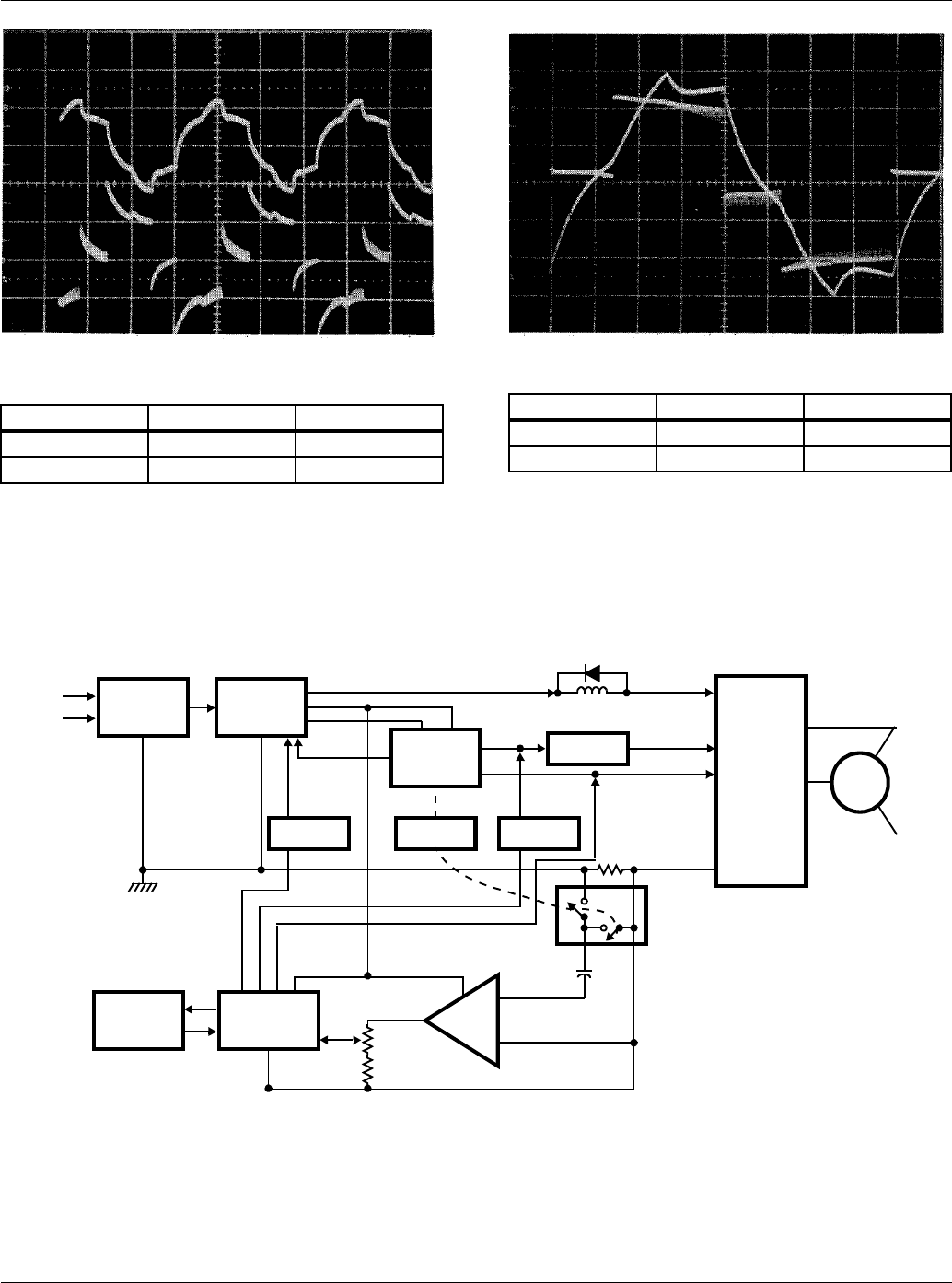
TRACE VERTICAL HORIZONTAL
A 5V/DIV 200µSEC/DIV
B 5V/DIV 200µSEC/DIV
TRACE VERTICAL HORIZONTAL
A 3A/DIV 200µSEC/DIV
B 5V/DIV 200µSEC/DIV
Application Note 7511
©2002 Fairchild Semiconductor Corporation Application Note 7511 Rev. A1
.
FIGURE 13A. MOTOR CURRENT AND VOLTAGE ARE SHOWN
HERE, FOR LIGHT LOADS FIGURE 13B. MOTOR CURRENT AND VOLTAGE ARE SHOWN
HERE, FOR HEAVY LOADS.
To complete the design of the 6-step motor drive, it’s necessary to consider protection circuitry for the output IGTs. The drive receives its
power from a switching supply already containing provisions for protection from line over-voltage and under-voltage and transient effects.
However, you still have to guard the power switches against unwanted effects on the output lines and the possibility of noise or other
extraneous signals causing gate-drive timing errors.
The best protection circuit must match the characteristics of the power switch and the circuit’s bias conditions. The IGT is very rugged
during turn-on and conduction, but it requires time to dissipate minority carriers when turning off high currents and voltages. An analysis
of the possible malfunction condition
FIGURE 14. THE LOWEST COST SENSOR IMAGINABLE, A PIECE OF COPPER WIRE SERVES AS THE CURRENT MONITOR IN THIS SYS-
TEM. THE CHOPPED AND AMPLIFIED VOLTAGE DROP ACROSS THE WIRE TRIGGERS A GATE-DRIVE SHUT-OFF CIRCUIT
UNDER FAULT CONDITIONS.
TRACE VERTICAL HORIZONTAL
A 1A/DIV 1mSEC/DIV
B 50V/DIV 1mSEC/DIV
TRACE VERTICAL HORIZONTAL
A 3A/DIV 2mSEC/DIV
B 100V/DIV 2mSEC/DIV
AC
LINE
INPUT
HV
DISABLE
GATE DRIVE TURNOFF
HV
ADJUST
50 TO 320V DC
5V DC UPPER 3
LOWER 3
dI/dt LIMIT
24V DC
CHOPPER
I LIMIT
10A
20A
ISOLATIONISOLATION
IGT
SWITCHES MOTOR
CONTROL
AND
TIMING
ISOLATION
RECTIFIER
AND
FILTER
SWITCHING
POWER
SUPPLY
RECYCLE
TIME COMPARATOR
AND LATCH
AC
AV = 100
ISOLATION
Application Note 7511
©2002 Fairchild Semiconductor Corporation Application Note 7511 Rev. A1
FIGURE 15A. THIS ALL-ENCOMPASSING PROTECTION SYSTEM PROVIDES THREE INDEPENDENT SHUTDOWN FUNCTONS -
ONE EACH FOR THE UPPER AND LOWER IGTS AND THE HIGH-VOLTAGE SUPPLY.
FIGURE 15B. THIS CIRCUIT PROVIDES CHOPPER DRIVE FOR THE COPPER-WIRE
SENSOR IN FIGURE 15A. FIGURE 15C. SHOWS THE HIGH-VOLT-
AGE SHUTDOWN CIRCUIT.
50 TO 320V DC
24V
3.9k
750k 3.3k
2.7k
2N5355
470pF
0.01µF
10A
2k
5µF
20V
150
2N5232
15V
5µF
25V
220k
2.2k
0.001
µF
H11F3
H11F3 TO
CONTROL CIRCUIT
39
470
pF
390
20A
2k
2mΩ (1” #24 AWG COPPER)
POWER
SUPPLY CURRENT
SENSE AND
CHOPPER
AC
AMPLIFIER LATCHING
FAST
COMPARATOR
10ms
RESET IGT POWER SWITCHES
A139M
50µH
10k
180k 47k 39k
0.001
µF
1k
2N5306
C203B
0.02
µF22k
H11AV2 TO PZO SHUTDOWN
H11AV2 TO HI-V SHUTDOWN
22
0.2µF
2
1
TO
DRIVE
DT230F
TO
MOTOR
TIMER
555
13
CHOPPER DRIVE
TO PIEZO
DRIVERS
5V
150150
180
0.002
µF
5.1k
2N5232
H11F3H11F3
100
180
0.002
µF5.1k
2N5232
0.005µF
150
DT230F
(3)
47k
H11AV2
10µF
10V
ALL OPTOCOUPLERS GO TO PROTECTION CIRCUIT
SG3524
15
16
10 8
HIGH-VOLTAGE SHUTDOWN
24V TO
CONTRO
L
5V
2.2k
0.005
µF
1M
Application Note 7511
©2002 Fairchild Semiconductor Corporation Application Note 7511 Rev. A1
Latch-Up: Hints, Kinks and Caveats
The IGT is a rugged device, requiring no snubber network
when operating within its published safe-operating-area
(SOA) ratings. Within the SOA, the gate emitter voltage
controls the collector current. In fact, the IGT can conduct
three to four times the published maximum current if it’s in the
ON state and the junction temperature is +150oC maximum.
However, if the current exceeds the rated maximum, the IGT
could lose gate control and latch up during turn-off attempts.
The culprit is the parasitic SCR formed by the pnpn structure
shown in Figure 16. In the equivalent circuit, Q1 is a power
MOSFET with a normal parasitic transistor (Q2) whose base-
emitter junction is shunted by the low-value resistance R1.
FIGURE 16. THE IGT’S PARASITIC SCR IS RESPONSIBLE FOR
THE DEVICE’S LATCH-UP CHARACTERISTICS.
For large current overloads, the current flowing through R1
can provoke SCR triggering. In the simplest terms, R1 repre-
sents the equivalent of a distributed resistor network, whose
magnitude is a function of Q2’s VCE. During normal IGT
operation, a positive gate voltage (greater than the thresh-
old) applied between Q1’s gate and source turns the FET on.
The FET then turns on Q3 (a pnp transistor with very low
gain), causing a small portion of the total collector current to
flow through the R1 network.
To turn the IGT off, you must reduce the gate-to-emitter
voltage to zero. This turns Q1 off, thus initiating the turn-off
sequence within the device. Total fall time includes current-
fall-time one (tF1) and current-fall-time two (tF2)
components. The turn-off is a function of the gate-emitter
resistance, Q3’s storage time and the value of VGE prior to
turn-off. Device characteristics fix both the delay time and
the fall time.
Forward-Bias Latch-Up
Within the IGT’s current and junction-temperature ratings,
current does not flow through Q2 under forward-biased
conditions. When the current far exceeds its rated value, the
current flow through R1 increases and Q3’s VCE also
increases because of MOSFET channel saturation. Once
Q3’s ICR1 drop exceeds Q2’s VBE(ON), Q2 turns on and
more current flow bypasses the FET.
The positive feedback thus established causes the device to
latch in the forward-biased mode. The value of IC at which
the IGT latches on while in forward conduction is typically
three to four times the device’s maximum rated collector
current. When the collector current drops below the value
that provokes Q2 turn-on, normal operation resumes if chip
temperature is still within ratings.
If the gate-to-emitter resistance is too low, the Q2-Q3
parasitic SCR can cause the IGT to latch up during turn-off.
During this period, RGE determines the drain-source dV/dt of
power MOSFET Q1. A low R1 causes a rapid rise in voltage -
this increases Q2’s VCE, increasing both R1’s value and Q2’s
gain.
Because of storage time, Q3’s collector current continues to
flow at a level that’s higher than normal for the FET bias.
During rapid turn-off, a portion of this current could flow in
Q2’s base-emitter junction, causing Q2 to conduct. This
process results in device latch-up; current distribution will
probably be less uniform than in the case of forward-bias
latch-up.
Because the gains of Q2 and Q3 increase with temperature
and VCE, latching current - high at +25oC - decreases as a
function of increasing junction temperature for a given gate-
to-emitter resistance.
How do you test an IGT’s turn-off latching characteristic?
Consider the circuit in Figure 17. Q1’s base-current pulse
width is set approximately 2µsec greater than the IGT’s gate-
voltage pulse width. This way, the device under test (DUT)
can be switched through Q1 when reverse-bias latch-up
occurs. This circuit allows you to test an IGT’s latching
current nondestructively.
The results? Clamped-inductive-load testing with and
without snubbers reveals that snubbering increases current
handling dramatically: With RGE = 1kΩ, a 0.02µF snubber
capacitor increases current capability from 6A to 10A; with
RGE = 5kΩ, a 0.09µF snubber practically doubles capacity
(25A vs 13A).
Conclusions? You can double the IGT’s latching current by
increasing RGE from 1kΩ to 5kΩ, and double it again with a
polarized snubber using CS < 0.1µF. The IGT is therefore
useful in situations where the device must conduct currents
of five to six times normal levels for short periods.
Finally, you can also use the latching behavior to your advan-
tage under fault conditions. In other words, if the device
latches up during turn-off under normal operation, you could
arrange it so that a suitable snubber is switched electroni-
cally across the IGT.
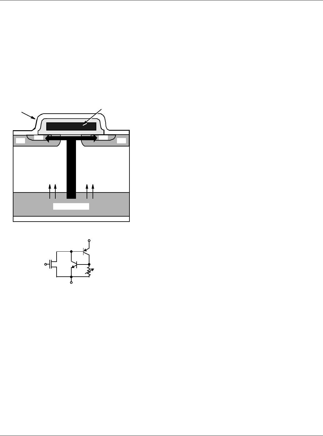
EMITTER METAL POLYSILICON GATE
P
METAL COLLECTOR
MINORITY
CARRIER
INJECTION
MAIN CURRENT PATH
N EPITAXIAL LAYER
P+ SUBSTRATE
N+N+
P
COLLECTOR
Q3
R1
EMITTER
GATE Q2
Q1
Application Note 7511
©2002 Fairchild Semiconductor Corporation Application Note 7511 Rev. A1
FIGURE 17. USE THIS LATCHING-CURRENT TESTER TO TEST IGTS NONDESTRUCTIVELY. Q1’S BASE-DRIVE PULSE WIDTH IS GREAT-
ER THAN THAT OF THE IGT’S GATE DRIVE, SO THE IGT UNDER TEST IS SWITCHED THROUGH Q1 WHEN REVERSE-BIAS
LATCH-UP OCCURS.
PULSE
GENERATOR
PULSE
GENERATOR
TRIGGER
1000pF
A114A
A114A 1k
100
100
50
10
D38H1
D44D6
Q1 = D66EV7
Q2 = DUT D94FQ4
DS0026x2
5V
1N914
10V
PE-63385
A114A
15V
D66EV7
Q1
RGE
1-10k
VCE
A139M
10
VCC
VCLAMP
(400V MAX)
0.02µF
10µF
A139P
L = 100µH
2k
Q2
Application Note 7511

DISCLAIMER
FAIRCHILD SEMICONDUCTOR RESERVES THE RIGHT TO MAKE CHANGES WITHOUT FURTHER
NOTICE TO ANY PRODUCTS HEREIN TO IMPROVE RELIABILITY, FUNCTION OR DESIGN. FAIRCHILD
DOES NOT ASSUME ANY LIABILITY ARISING OUT OF THE APPLICATION OR USE OF ANY PRODUCT
OR CIRCUIT DESCRIBED HEREIN; NEITHER DOES IT CONVEY ANY LICENSE UNDER ITS PATENT
RIGHTS, NOR THE RIGHTS OF OTHERS.
TRADEMARKS
The following are registered and unregistered trademarks Fairchild Semiconductor owns or is authorized to use and is
not intended to be an exhaustive list of all such trademarks.
LIFE SUPPORT POLICY
FAIRCHILDS PRODUCTS ARE NOT AUTHORIZED FOR USE AS CRITICAL COMPONENTS IN LIFE SUPPORT
DEVICES OR SYSTEMS WITHOUT THE EXPRESS WRITTEN APPROVAL OF FAIRCHILD SEMICONDUCTOR CORPORATION.
As used herein:
1. Life support devices or systems are devices or
systems which, (a) are intended for surgical implant into
the body, or (b) support or sustain life, or (c) whose
failure to perform when properly used in accordance
with instructions for use provided in the labeling, can be
reasonably expected to result in significant injury to the
user.
2. A critical component is any component of a life
support device or system whose failure to perform can
be reasonably expected to cause the failure of the life
support device or system, or to affect its safety or
effectiveness.
PRODUCT STATUS DEFINITIONS
Definition of Terms
Datasheet Identification Product Status Definition
Advance Information
Preliminary
No Identification Needed
Obsolete
This datasheet contains the design specifications for
product development. Specifications may change in
any manner without notice.
This datasheet contains preliminary data, and
supplementary data will be published at a later date.
Fairchild Semiconductor reserves the right to make
changes at any time without notice in order to improve
design.
This datasheet contains final specifications. Fairchild
Semiconductor reserves the right to make changes at
any time without notice in order to improve design.
This datasheet contains specifications on a product
that has been discontinued by Fairchild semiconductor.
The datasheet is printed for reference information only.
Formative or
In Design
First Production
Full Production
Not In Production
MICROWIRE
OPTOLOGIC
OPTOPLANAR
PACMAN
POP
Power247
PowerTrench
QFET
QS
QT Optoelectronics
Quiet Series
FAST
FASTr
FRFET
GlobalOptoisolator
GTO
HiSeC
I2C
ISOPLANAR
LittleFET
MicroFET
MicroPak
Rev. H5
â
ACEx
Bottomless
CoolFET
CROSSVOLT
DenseTrench
DOME
EcoSPARK
E2CMOSTM
EnSignaTM
FACT
FACT Quiet Series
SILENT SWITCHER
SMART START
SPM
STAR*POWER
Stealth
SuperSOT-3
SuperSOT-6
SuperSOT-8
SyncFET
TinyLogic
TruTranslation
ââ
â
STAR*POWER is used under license
UHC
UltraFET
VCX
â
