Fairfield BOX-BASE Geophysical Data Telemetry System User Manual BS App 5
Fairfield Industries Inc Geophysical Data Telemetry System BS App 5
Operating Manual

THE BOX - Base Station Application for FCC Certification
Operating Manual
Appendix 5 Page 0 of 33
Appendix 5
Base Station Radio System

THE BOX - Base Station Application for FCC Certification
Operating Manual
Appendix 5 Page 1 of 33
Appendix 5
Contents
1.0 Base Station Modules
2.0 Radio Command Unit (RCU)
2.1 Overall Description
2.3 Baseband Module
3.3.1 Overall Description
2.3.2 Circuits and Function
2.3.2.2 DSP and Memory
2.3.2.2 Digital I/O, RCB. RS-232 and Timer
2.3.2.3 Codec and Clock Generation
2.3.2.4 FPGA and Seismic Data Bus
2.4 Clock Generator and Splitter Module
2.4.1 Overall Description
2.4.2 RF Splitter Sub-Module
2.4.3 Clock Reference Generator Sub-Module
2.4.4 RCU and DRU Versions
2.5 Power Amplifier Module
2.5.1 Overall Description
2.5.3 Power Amplifier Sub-Module
2.5.3.1 DC Null
2.5.3.2 RF Attenuation
2.5.4 Linearizer Sub-Module
2.5.4.1 Linearizer Operation
2.5.4.2 Instability Detection
2.5.5 Control Sub-Module
2.5.5.1 Feedback Coupler
2.5.5.2 Transmit/Receive Switching
2.5.5.3 Dallas Temperature Sensor
2.5.6 MHU Power Conditioning & Current Sensor
2.5.7 RF Transmission Specifications
2.6 Power Supply Module
2.6.1 Inputs
2.6.2Outputs
3.0 Data Receive Unit (DRU)
3.1 Overall Description
3.2 Concentrator Module
3.2.1 Specifications
3.3 RF Module
3.3.1 Overall Description

THE BOX - Base Station Application for FCC Certification
Operating Manual
Appendix 5 Page 2 of 33
3.3.2 RF Modules in RCU and DRU
3.3.2.1 Use in RCU
3.3.2.2 Use in DRU
3.3.3 Dual Synthesizer
3.3.4 RF Receiver
3.3.5 ADC
4.0 Masthead Unit (MHU)
4.1 Circuits and Functions
4.1.2 Power Conditioning
4.1.3 TX/RX Switching
4.1.4 Low-Noise Amplifier and Band-Pass Filter
4.1.4.1 Low-Noise Amplifier
4.1.1.2 Band-PassFilter
5.0 Signals & Connections
5.1 RCU
5.3 RF Module
5.4 Baseband Module
5.5 Buses
5.6 Concentrator Module
5.7 Power Supply Module
THE BOX - Base Station Application for FCC Certification
Operating Manual
Appendix 5 Page 3 of 33
1.0 Base Station Modules
The Base Station, which is part of the Central Recording System (CRS), comprises three principal
modules: The Radio Command Unit (RCU), the Data Receive Unit (DRU) and the Mast-Head Unit
(MHU). The Central Recording System also contains the Recording Computer.
2.0 Radio Command Unit (RCU)
2.1 Overall Description
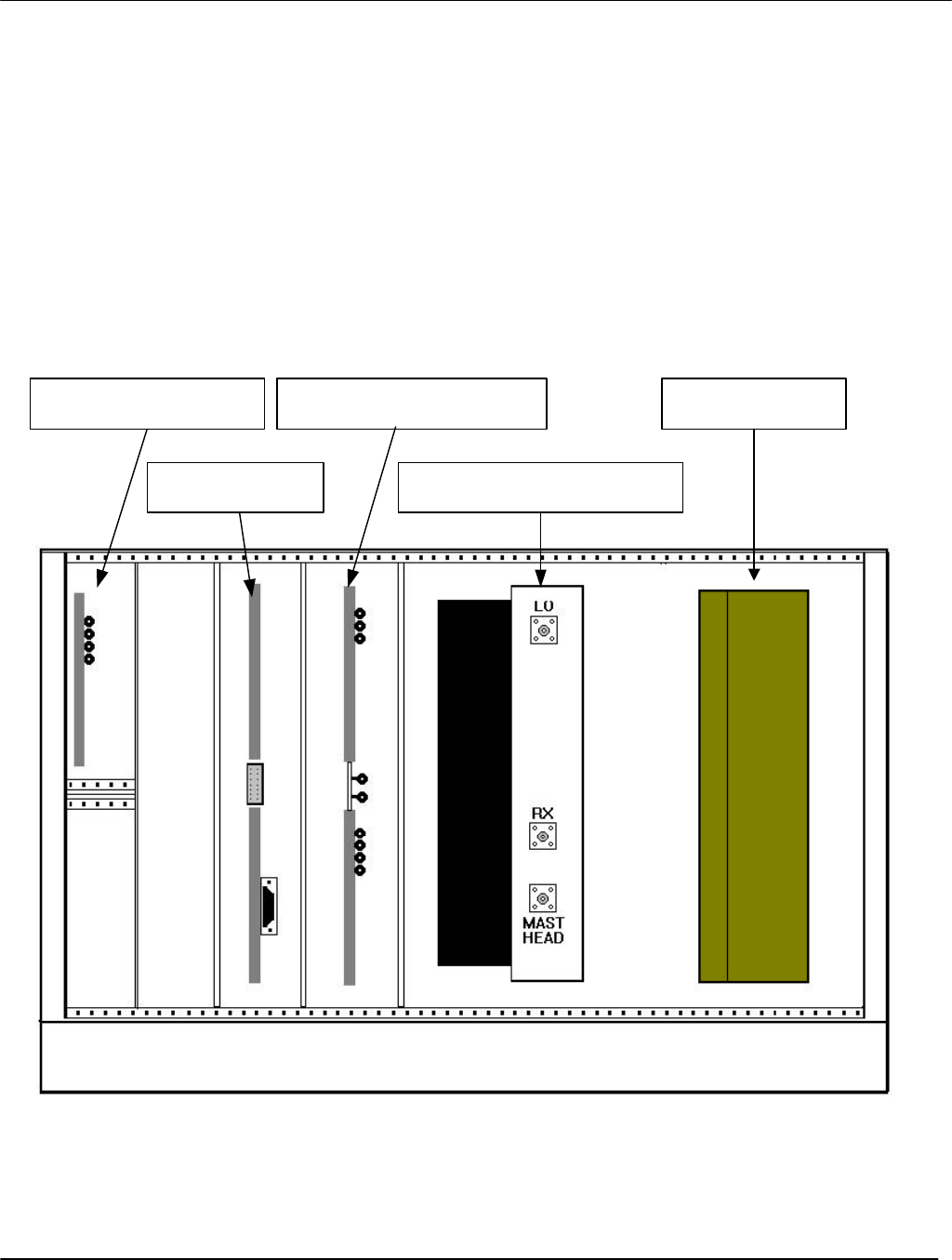
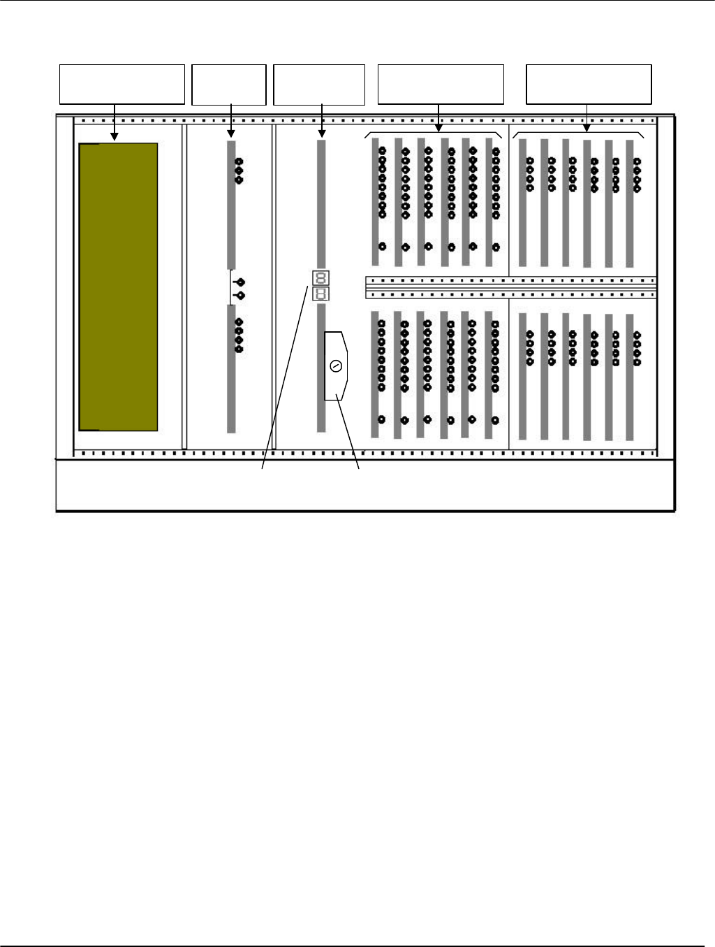
Figure 1 shows the names and locations of the various modules in the RCU, together with the Section
of this text in which they are described.
Front View of Radio Command Unit
Figure 1
Single-Channel Receiver
3.3
Base-Band Board
2.3
Clock Generator and Splitter
2.4
Power Amplifier (Transmitter)
2.5
Power Supply Unit
2.6
THE BOX - Base Station Application for FCC Certification
Operating Manual
Appendix 5 Page 4 of 33
The Radio Command Unit is a Base Station module which houses a single-channel transmitter for the
Command downlink and a single-channel receiver for Command uplinks. The unit also houses the
Master Frequency Reference Generator for the System and provides distribution of both the Master
Frequency Reference and the received RF to multiple Data Receiver Units (DRU).
The RCU interfaces with the Recording Computer and the DRUs via a Radio
Control Bus (RCB), and provides an interface to the Recording Computer’s
data bus for single-channel seismic data capture.
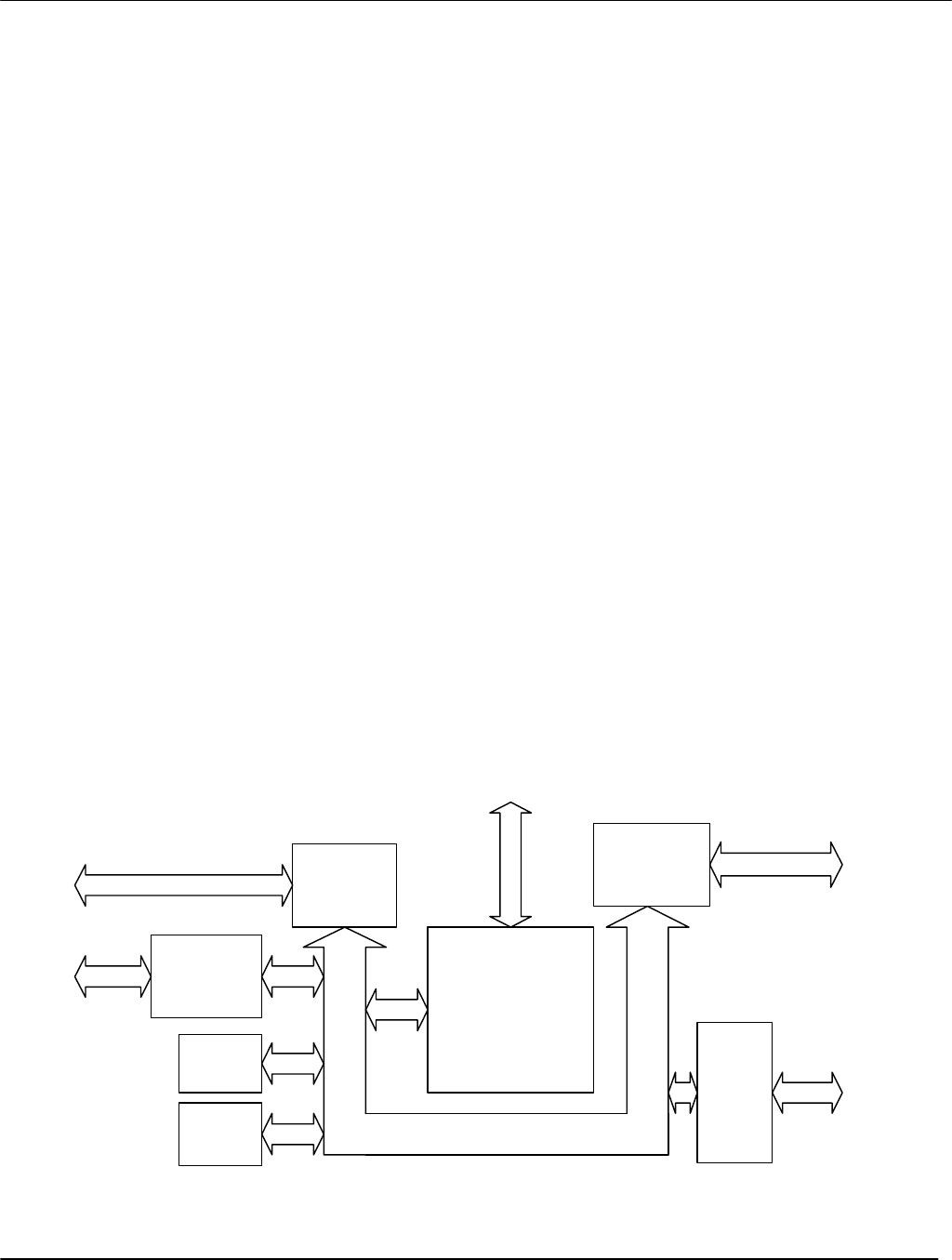
2.3 Baseband Module
There is one baseband board in the RCU and up to twelve in the DRU. Each baseband module
formats data and commands received from its corresponding RF board.
2.3.1 Overall Description
The Command baseband module is shown in block form in figure 2. It provides all digital processing for
both the Power Amplifier Module and the Command Receiver in addition to performing recorder control
functions.
The module receives command and configuration information from the Control Interface Board through
the Radio Control Bus, and passes Command Unit status information back to the Control Interface
Board.
The Command Base-Band module consists of four separate sub-modules:
DSP and Memory;
Digital I/O, RCB, RS232 and Timer;
CODEC and Clock Generation; and
FPGA and Seismic Data Bus.
DSP
TMS320C50
UARTRS232
Bus I/FRadio Control Bus
Codec
Digital
I/O
Controller Digital I/O
RAM
FLASH Data Bus
Bus I/F Radio Data Bus
Command Unit Base-Band Module - Block Diagram
Figure 2

THE BOX - Base Station Application for FCC Certification
Operating Manual
Appendix 5 Page 5 of 33
2.3.2 Circuits and Functions
2.3.2.1 DSP and Memory
The DSP is a single digital signal processor (type TMS320C50) with ancillary memory and peripherals.
This DSP has 16-bit address lines and 16-bit data lines. Its clock is 40.00 MHz, which is obtained from
the Clock Generation sub-section.
There are four 64k X 4 RAM ICs which are used for memory. In addition, a Flash Memory contains
configuration information for the DSP.
DSP outputs include:
16 data bits (D0 to D15) which go to the Universal Serial Controller (USC),
CODEC-DACDATA connected to the CODEC sub-section, and
Control and clock signals for the FPGA, USC, Timer and UART.
2.3.2.2 Digital I/O, RCB, RS-232 and Timer (See Schematic ---)
The USC (type A16C30V10VSC) interfaces with the DSP through the16-bit data lines (D0-D15).
A Master to Slave signal is placed on the RCB to interface with the Command Unit and the DRUs.
U35 and associated components form the timer circuitry using the crystal oscillator X2, at a frequency
of 32.768 kHz.
Inputs to the Digital I/O circuits from the Command Transmitter board include:
Cartesian transmitter instability detector,
VSWR alarm indicator, and
Transmitter Temperature indicator.
Digital outputs include:
Synth Serial Data and Synth Serial Data clock to the Synthesizer of the Command RF board.
Cartesian loop gain reduction and Cartesian loop dc null control signals to the Cartesian Linear
Transmitter of the Command Transmitter board.
U36 is a Universal Asynchronous Receiver and Transmitter (UART) which provides an RS232 link for
test purposes.
2.3.2.3 CODEC and Clock Generation (See Schematic ---)
The CODEC U32 provides A/D conversion of the up-linked I and Q signals to CODEC serial data. This
serial data is routed to the Command Base-Band board for processing.

THE BOX - Base Station Application for FCC Certification
Operating Manual
Appendix 5 Page 6 of 33
The CODEC also performs A/D conversion of the CODEC serial data (from the Command Base-Band
board) into I and Q Base-Band signals. These I and Q signals are sent to the Power Amplifier Module
for modulation and transmission.
The CODEC clock is 7.68 MHz, and is derived from the 61.44 MHz VCO and the Divide by Eight
Counter, U21.
The P-CLK signal for the DSP is 40 MHz. A jumper selection at Jumper Point JP9, permits selection of
40 MHz from either X1 (the internal oscillator) or from the 40 MHz Master Clock from the RF Splitter
board.
This sub-section takes the RX-I and RX-Q signals from the Command Receiver board and converts
them to CODEC serial data to be sent to the DSP for processing.
The A/D conversion involves converting the CODEC-DACDATA from the DSP to TX-I and TX-Q
Cartesian Base-Band signals to be fed to the Cartesian Linear Amplifier on the PA Linearizer board.
Phase-Control (PH-CTL) signal is also fed to the PA Linear Amplifier to maintain a phase balance
between the I and Q signals.
2.3.2.4 FPGA and Seismic Data Bus (See Schematic ---)
U3 is a Field-Programmable Gate Array (FPGA) which contains the I/O and digital logic functions and
also provides the interface between the DSP and the Control Interface Board.
2.4. Clock Generator & Splitter Module
2.4.1 Overall Description
The two main sub-modules within this board are the
RF Signal Splitter and the
Reference Generator.
There are two versions of the Clock Generator & Reference module: one in the RCU and the other in
each DRU.
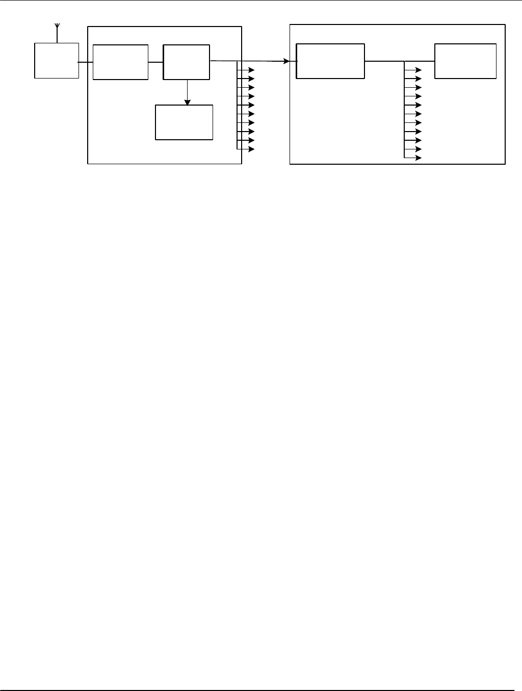
• The Command Unit contains a module which splits the received RF signals 12 ways, for distribution
as shown in figure 3.
This module generates a 40 MHz controlled-reference clock which is fed to the Command Receiver
and to up 11 DRUs.
• Each DRU contains a module which serves:
• to split the Reference Clock two ways for distribution to the RF and Baseband boards within the
DRU and
• to split received RF signals twelve ways for distribution to RF boards within the DRU.
THE BOX - Base Station Application for FCC Certification
Operating Manual
Appendix 5 Page 7 of 33
Received RF Signal Path showing Distribution Functions of RF Splitter
Figure 3
As shown in figure 3, the antenna feed to the RCU version of this module comes from the Mast-Head
Unit via the antenna interface, whilst the antenna feed to the DRU version comes from the RF output of
the Command Unit splitter.
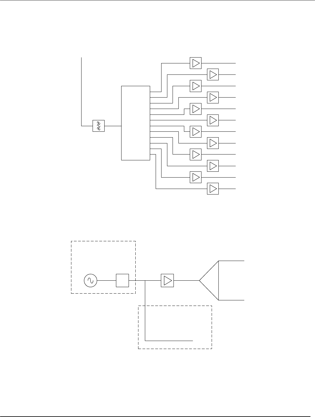
2.4.2 RF Splitter Sub-Module
Figure 4 shows that the RF splitter stages consist of
antenna feed,
filter,
power division and
twelve 12 dB gain stages.
The band-pass filter on the splitter board ensures that no in-band intermodulation is produced by out-of-
band energy.
The filtered signal is fed into a 12-way splitter. In order to compensate for the insertion loss of this
splitter, a 12 dB (nominal) gain stage is present in each RF output path. This results in 12 RF outputs
of a level nominally identical to the RF input level – giving a 0dB gain stage.
2.4.3 Clock Reference Generator Sub-Module
Figure 5 illustrates the differing reference clock configurations of the CU and the DRU splitter variants.
In the CU model an on-board highly-stable oven-controlled oscillator provides the reference
signal. The DRU model does not possess this oscillator and requires the clock signal to be
sourced from the backplane.
Mast-
Head
Unit
Antenna
Interface RF
Splitter
RF Splitter &
Reference
Distributor
1
2
3
4
5
6
7
8
9
10
11
12
RF and
Base-Band
Boards
Antenna
RF
Command
Receiver
11 DRUs max 12 RF Boards and
12 Base-Band Boards
in each DRU
Command Unit Data Receiver Unit #1
To RF & Base-
Band Boards
2
3
4
5
6
7
8
9
10
11
To DRUs
1
THE BOX - Base Station Application for FCC Certification
Operating Manual
Appendix 5 Page 8 of 33
The gain stage provides an output of approximately +17 dBm which, when split through a tuned
Wilkinson power divider, results in a nominal +13 dBm signal at both 40 MHz reference points. The CU
RF board uses one of the reference signals and the second is used by any connected DRU.
RF Splitter Stages
Figure 4
MINI CIRCUITS
PSC-12-11-1
12-Way
Splitter
MOTOROLA
MRF553
12dB Gain Stages
Filter
Antenna
RF1
RF2
RF3
RF4
RF5
RF6
RF7
RF8
RF9
RF10
RF11
RF12
DRU ONLY
40 MHz Backplane Feed
Command Unit Only
40 MHz OCXO
dB
BPP193 Gain Stage
WILKINSON
Power Divider 40 MHz REF1
40 MHz REF2
Reference Generator
Figure 5

THE BOX - Base Station Application for FCC Certification
Operating Manual
Appendix 5 Page 9 of 33
2.4.4 RCU & DRU Versions of Clock Generator & Splitter Modules
As has been shown in figure 5, there are two versions of this module. Physical differences are detailed
in Table 1.
Component Radio Command Unit Data Receiver Unit
Reference oscillator 40 MHz present Not present
Oscillator link Pins 1 & 3 linked Pins 2 & 3 linked
Handle colors Blue Black
Clock Generation & Splitter Board: CommandUnit/Data Receiver Unit Differences
Table 1
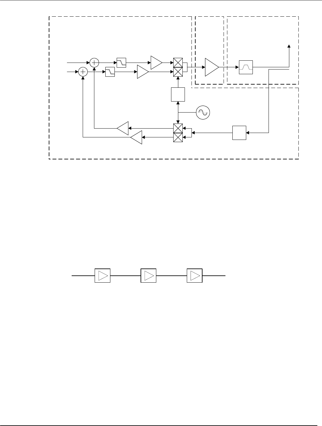
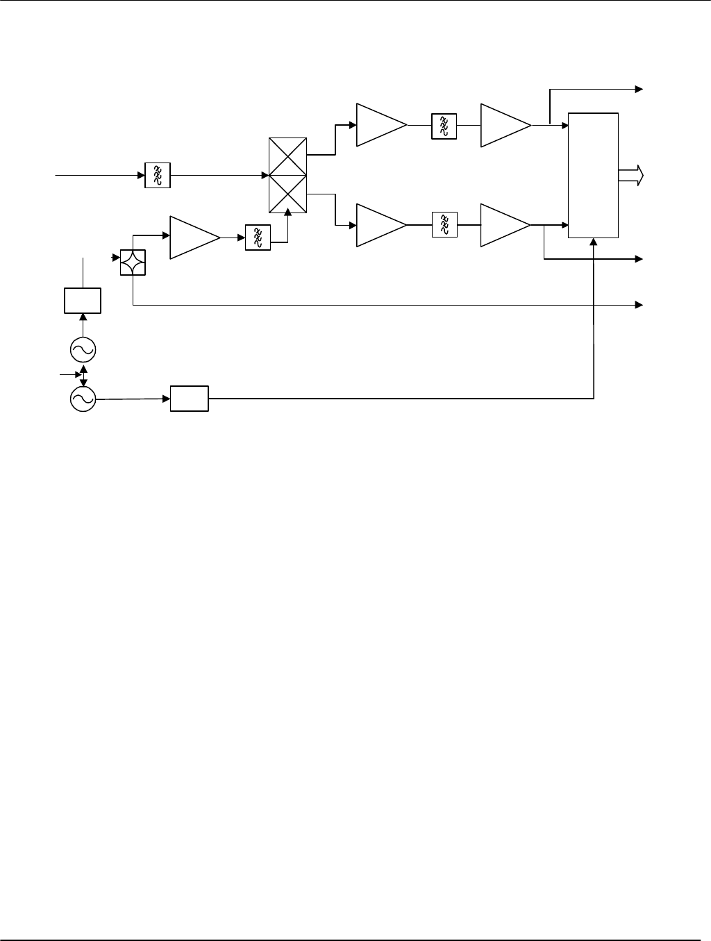
2.5 Power Amplifier Module
2.5.1 Overall Description
This module comprises the transmitter that feeds RF to the antenna for downlinking commands to the
Remote Units, and is illustrated in figure 6.
The module contains three separate sub-modules, all located on the same board:
Power Amplifier A three stage power amplifier which provides the RF forward-path gain and
final output drive for the RCU transmitter.
Cartesian Linearizer RF and baseband processing sub-module which provides direct up-conversion
of the quadrature baseband input signals, while simultaneously correcting for
non-linearities in the power-amplifier.
Control Section This sub-module provides a 20 dB (nominal) RF feedback path to the Cartesian
Loop Linearizer as well as transmit-receive switching and MHU (masthead)
power supply conditioning. Also incorporated are:
A temperature sensor,
Non-volatile parameter storage,
Masthead connection status and VSWR indication.
2.5.2 Dedicated Channel
The RCU downlink requires a single 20 kHz dedicated channel. The transmission of a pilot on this
channel provides a means of waking up the remote units and frequency locking them to the CRS high-
stability reference.
THE BOX - Base Station Application for FCC Certification
Operating Manual
Appendix 5 Page 10 of 33
Linearized Power Amplifier - Block Diagram
Figure 6
2.5.3 Power Amplifier Sub-Module
The PA sub-module comprises the main RF amplifier and provides the forward-path gain and final
output drive. This board consists of three ‘Semelab’ device stages, shown in fig. 7.
D2019UK D1013UK D1020UK
28V @ 250mA
23dB Gain 28V @ 750mA
23dB Gain 28V @ 1.0A
14dB Gain
PA Device Line-Up
Figure 7:
Each device is individually tuned for gain and return loss. The whole line-up is tuned to achieve a gain
of approximately 60dB.
2.5.3.1 DC Null
During operation of the PA, a steadily rising carrier component exists on the output spectrum, this being
a result of carrier up/down-converter feed-through. It can be seen at baseband as a dc component
superimposed on the I and Q signals.
PA Control
I
Q
up-
converter
down-
converter
RF
amplifier harmonic
filter
RF
attenuator
dB
feedback
gain
lowpass
filter
local
oscillator
- -
φRF phase
shifter
directional
coupler
RF
output
pre-
amplifier
Linearizer
RF feedback
THE BOX - Base Station Application for FCC Certification
Operating Manual
Appendix 5 Page 11 of 33
This represents an unwanted tone in the output spectrum, and is removed by sampling the magnitude
of dc component at start of transmission and removing it from the resulting dc component 30 seconds
after transmission.
2.5.3.2 RF Attenuation
Transmitted power can be varied by a series of switchable attenuators situated in the Up- and Down-
Converter paths (figure 8), and is also controlled by the feedback gain elements.
Increasing the feedback gain reduces the overall output power.
To maintain linearization, the attenuator situated in the Up-Converter path must be changed in
the opposite direction to the attenuator in the Down-Converter path..
2.5.4 Linearizer Sub-Module
The basic layout of the linearizer is shown in fig. 8.
Linearizer – Block Diagram
Figure 8
φ
dB
dB
τ
I
Q
Low-pass filters
Local Oscillator
Phase-shifter
Delay Line
RF feedback from
Directional Coupler
RF
Modulation
Feedback Gain
Sample and Hold
Switchable
attenuator
Switchable
attenuator
Up-
Converter
Down-
Converter

THE BOX - Base Station Application for FCC Certification
Operating Manual
Appendix 5 Page 12 of 33
2.5.4.1 Linearizer Operation
A fraction of the transmitted RF signal is fed back from the output by the directional coupler (figures 6 &
8), and is then attenuated to reduce the signal to a level suitable for input to the down-converter.
The signal is split as shown and down-converted, with two carriers of 90º phase difference yielding the I
and Q baseband signals.
Feedback gain is provided by low-noise operational amplifiers (CLC428), and the signal is then
subtracted from the modulation input.
The forward path signal is low-pass filtered and pre-amplified at baseband. The baseband signal is
then up-converted with a phase-shifted version of the local oscillator to ensure that the input and
feedback signals are exactly 180° out of phase.
2.5.4.2 Instability Detection
To monitor loop stability during operation, a circuit is provided which measures output spectrum energy
around 200 kHz above the carrier.
Any instability causes high frequency components to appear in the output spectrum and
correspondingly at baseband level.
A high-pass filter is used to isolate these higher frequencies which are then fed through an
amplitude detector.
When the amplitude reaches a preset dc detected level, an instability error is flagged.
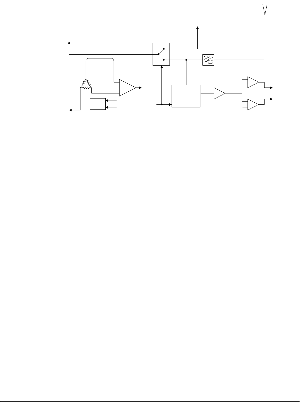
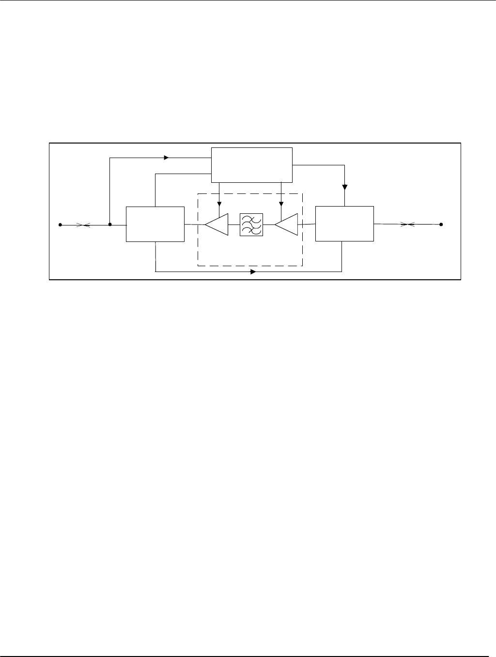
2.5.5 Control Sub-Module
The Control Sub-Module is shown in figure 9.
It provides RF feedback from the PA sub-module to the linearizer sub-module, and controls
transmit/receive switching.
Another function of this sub-module is to provide data storage of temperature-sensing and amplifier-
characterisation information by use of a Dallas temperature sensor and non-volatile memory device
2.5.5.1 Feedback Coupler
The Control Sub-Module provides a 20 dB-coupled path. A portion of the output signal, roughly 20dB
down, is sampled providing the feedback signal for the linearizer. A VSWR detection circuit enables
coupled and direct powers to be compared.
2.5.5.2 Transmit/Receive Switching
PIN diodes are used to direct signals from the antenna in receive and to the antenna during transmit.
THE BOX - Base Station Application for FCC Certification
Operating Manual
Appendix 5 Page 13 of 33
Harmonic
Filter
+15/-15V
Switchable
Supply
TX/RX
Antenna
Received
Signal
VREF1
VREF2
Transmit/Receive
switch
RF_IN
Resistive
Splitter
RF_FB
RX_HI
RX_LO
Current-to-Voltage
Converter
VSWR
DALLAS SDA
SCL
Control Sub-Module – Block Diagram
Figure 9
The diodes may be biased + (RX) or – (TX) by transistor switching between the two voltage rails.
The RF path is determined by the biasing of the PIN diodes which, in conjunction with matching
circuitry, act as RF quarter wavelength sections. These sections have the ability to behave as
open circuits or as 50Ω lines depending on the bias voltage.
The bias voltage also supplies masthead power via a dc-coupled link though the Masthead coaxial
cable.
2.5.5.3 Dallas Temperature Sensor
The Dallas sensing device provides a temperature measurement system, with one-second acquisition
time, the data being read as an integer byte. It also incorporates 256 bytes of non-volatile memory for
storing details unique to the individual amplifier – such as phase control voltages, phase, image
balance settings, serial number and revision details.
2.5.6 MHU Power Conditioning & Current Sensing
A dc supply rail powers the MHU (masthead unit) via the PA/Masthead coaxial cable.
The masthead’s own internal TX/RX switching is biased from this cable and, in Receive, a low-noise
amplifier with a 30 dB gain is powered.
The MHU is biased by either a positive or negative supply depending on the logic condition of the
TX/RX line.
In Transmit, the supply rail is negative, and the pin diodes in the RX path are biased to present
an open-circuit to RF, thereby ensuring that RF signal follows the TX path.

THE BOX - Base Station Application for FCC Certification
Operating Manual
Appendix 5 Page 14 of 33
In Receive, the supply rail is positive, and the RX path is enabled by positively-biased pin
diodes thereby allowing received RF to follow the RX path.
Current sensing is provided to monitor the presence and status of the MHU.
When the MHU is in Transmit mode, the current drawn is approximately 50 mA.
When the masthead is in Receive mode, the current drawn is approximately 450 mA.
Two comparator circuits are employed to give a logic low signal when MHU current is less than 50 mA
or greater than 500 mA.
The current sensor operates by using a current-to-voltage circuit which monitors the voltage dropped
across a very low-value resistor network. An operational amplifier provides a DC output between 0 and
5 V depending on the current drawn. This is fed into two level-set comparators, which provide the logic
signals.
2.5.7 RF Transmission Specifications
All output powers are defined at the masthead antenna connector.
2.5.7.1. RF Output Power
Mean: 10 W (+40 dBm +/- 1dB) available at antenna connector
2.5.7.2 RF Gain
60 dB ± 1 dB nominal
2.5.7.3 Supply Voltage
+ 28V ± 0.5 V @ 4.0A
2.5.7.4 Input Impedance
50 Ω nominal
2.5.7.5 Third order Intercept Point
55 dBc min.
(Measurement: two tones with 10 kHz spacing: 38 dBm per tone)
2.5.7.6 Harmonics
-70 dBc, 10 W cw output
2.5.7.7 Spurious
-70 dBc, 10 W cw output
THE BOX - Base Station Application for FCC Certification
Operating Manual
Appendix 5 Page 15 of 33
2.5.7.8 VSWR
Stable into 5:1 loads, all angles
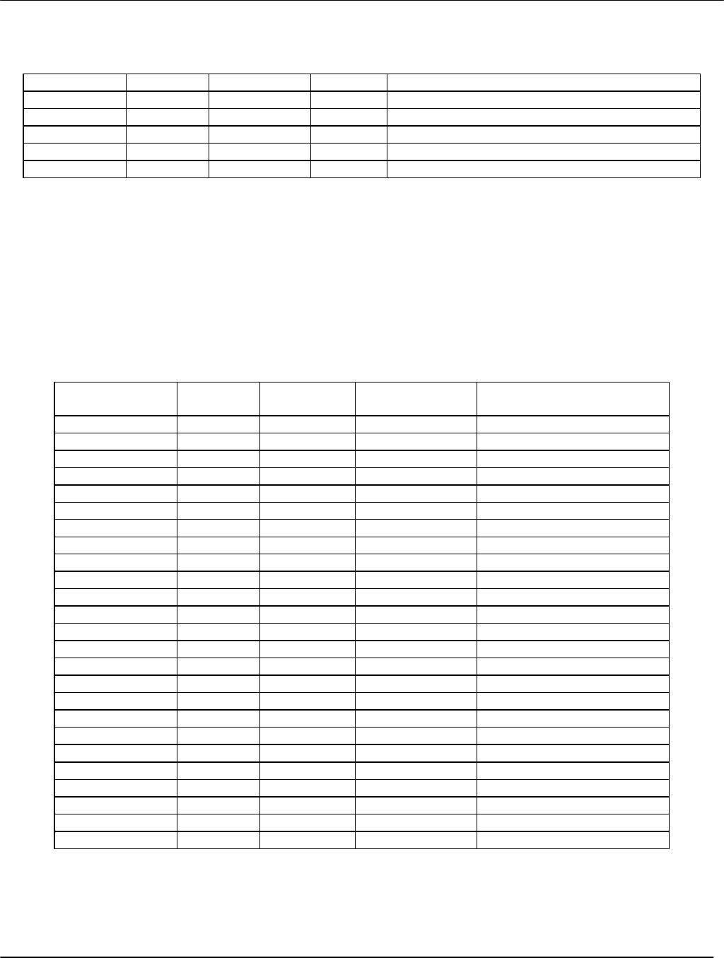
2.6 Power Supply Module
2.6.1 Inputs
240 V ac, 50/60 Hz or
120 V ac, 50/60 Hz
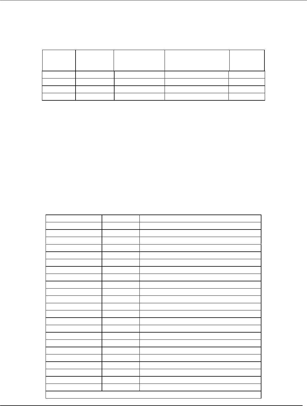
2.6.2 Outputs
Dc output voltages are given in Table 1.
Voltage
(V dc) Current
(A dc) Line Regulation
For 10% change
(%)
Load Regulation
For 10-100% change
(%)
Max Ripple
%
+5 4< 0.2 < 0.5 < 0.5
+15 4< 0.5 < 5 < 2
-15 4< 0.5 < 5 < 2
+28 10 < 0.5 < 5 < 2
PSU Output DC Voltages
Table 2
3.0 Data Receive Unit (DRU)
3.1 Overall Description
The DRU (Data Receive Unit) receives, demodulates, and decodes all seismic-trace data from the
seismic sensors and supplies this data through a Concentrator to the Recording Computer.
Figure 10 shows the names and locations of modules within each DRU, together with the section of this
text in which they are described:
3.2 Concentrator Module
Each DRU contains one Concentrator board which collects 8 channels of seismic data from each of the
12 data receiver board pairs (RF and Baseband boards).
The data are buffered and formatted for collection in multiplexed form over the Radio Data Bus (RDB)
by the Radio Data Interface board in the recording module (RDB). The Radio Data Interface is under
control of the Recording Computer.
A simplified functional diagram is shown in figure 11, and a block schematic in figure 12.
THE BOX - Base Station Application for FCC Certification
Operating Manual
Appendix 5 Page 16 of 33
The Concentrator polls each of the RF boards in the DRU in turn, waiting for all boards to have data
ready for collection. The Concentrator then clocks data out of each RF Board, with each channel
represented as two 16-bit words, into a FIFO buffer on the back-plane bus. The recording computer
then clocks this data onto the VME bus, with each 32-bit word represented as two 16 bit words
The Concentrator module determines which channels the DRU receives. On the front of the Concentrator
board there are two numeric LED displays and one rotor switch (figure 10). The switch is used to set the
DRU address from 0 to15.
Addresses 0 -10 are used for normal recording,
Addresses 11-14 are not used, and
Address 15 is used for single channel recording only.
The DRU address is displayed on the Concentrator numeric LED, address 0 being displayed as DRU 1,
address 1 as DRU 2, etc.
Front View of Data Receiver Unit (DRU)
Figure 10
Power Supply Unit
2.6 RFSplitter
2.4 Concentrator
3.2 Base-Band Boards
2.3 RF Boards
3.3
1 16 6
7 712 1211 111010 9 98 8
2 23 34 45 5
LED Displays of
DRU Numbers Address
Rotor Switch
THE BOX - Base Station Application for FCC Certification
Operating Manual
Appendix 5 Page 17 of 33
Simplified Received Data Transfer
Figure 11
Data Rx 0 Data Rx 11
Concentrator
Recording Computer
VME Interface
16
8
4
Data
Data Rx Rack Address
Run
Clk
Data + Rx Board &
Channel Address
Control
8
16
Reset
Data
Present
Concentrator Module – Block Schematic
Figure 12
Base-Band
Boards (12) RF
Boards(12) Concentrator Radio Data
Interface
Memory
Recording
Computer
VME
BUS

THE BOX - Base Station Application for FCC Certification
Operating Manual
Appendix 5 Page 18 of 33
3.2.1 Specifications
3.2.1.1 Gain & Noise
Gain: For each signal path, 0 dB nominal (independent of the number of properly
terminated outputs).
Noise: For each RF signal path < 20 dB.
3.2.1.2 Maximum Input Power
RF input: +10 dBm, 1 dB compression.
3.2.1.3 Third Order Intercept Point
RF input: ≥ +36 dBm.
3.2.1.2 Reference Signals
40 MHz Oscillator: Stability < 1 ppm (used in CU splitter card only)
40MHz ref. output #1: Level 13 dBm
40MHz ref. output #2: Level 13 dBm
40 MHz ref. input: Input level 13 dBm (used in DRU splitter board only).
3.3 RF Module
3.3.1 Overall Description
The RF module provides the RF receive chain for uplinks from remote units to the CRS. This board is
used in two racks:
One RF module board is used in the RCU, and
up to 12 RF module boards are used in each DRU. Each of these RF boards is used in
conjunction with an associated DRU board, also located in the DRU.
The module contains an ac-coupled direct-conversion receiver suitable for 16QAM data. The board
also incorporates the RF synthesizer, which is used in both the receiver and the command unit
transmitter.
Principal functions are summarized as follows:
RF Receiver The receiver provides linear direct down-conversion from the RF channel
frequency to quadrature baseband outputs.
Dual Synthesizer One synthesizer provides a Local Oscillator (LO) for both the receiver
sub-module and the command transmitter module. The other syntheziser
provides the clock for the ADCs. The synthesizer reference is derived
from the CRS high-stability source.
THE BOX - Base Station Application for FCC Certification
Operating Manual
Appendix 5 Page 19 of 33
ADC The ADC (Analog to Digital Converter)serves to digitize the received
baseband I and Q signals. The resulting data are output serially.
Down
Converter
Low-noise
gain stages
Dual
synthesizer
RF_IN
LO
driver
ADCs SERIAL
DATA
A/D clock
PA LO
DIVIDE
BY 4
DIVIDE
BY 4
40MHz
REF
+27 dBm LO
856-936 MHz
92.16 MHz 23.04 MHz
214-234 MHz
Active
filters Final
gain stage
RF (Receiver) Board
Figure 13
3.3.2 RF Module in RCU and DRU
3.3.2.1 Use in RCU
When used in the radio command unit, the Baseband I and Q signals are output, and the ADCs are not
used.
In this mode, the receiver receives a single 20 kHz channel, which is digitized by the RCU Unit
baseband module (reference Section 2.3). It should be noted that the dual-synthesizer. In the RF
module is programmed by the Baseband board.
The LO signals are used by the receiver down-conversion process and output to the RCU Power
Amplifier (Transmitter) module.
3.3.2.2 Use in DRU
When used in a DRU, each RF module is used in conjunction with its own associated baseband
module in the DRU.
Each RF module is used to receive up to 8 contiguous 20 kHz channels,
The analog to digital converters (ADC) operate at a sampling rate of 180 kHz to convert the baseband
I and Q signals and output the result as a serial data stream to the DRU Baseband board.

THE BOX - Base Station Application for FCC Certification
Operating Manual
Appendix 5 Page 20 of 33
The DRU Baseband board programs the dual synthesizer. The LO signals are used only by the
receiver down-conversion process.
3.3.3 Dual Synthesizer
The dual synthesizer package enables the clock signals of both the down-converter LO and the ADC to
be derived from the single oven-controlled stable source provided by the CRS splitter.
Serial programming of the LMX2332 enables 10 kHz steps from 216.01 to 213.99 MHz to be
synthesized. The synthesizer design employs an 856-936 MHz VCO running at four times the RF
down-conversion frequency. As can be seen in figure 13, a divide-by-four stage reduces the LO signal
frequency to the required band.
The RF LO is fed into a Wilkinson power divider
One output of this divider supplies a nominally 0 dBm LO for use by the PA module.
The other output is fed through an amplifier to a Semelab D2081UK, which provides a +27
dBm LO. This LO is used by the high third order intercept-point down-converter (Mini-Circuits
JSIQ-234DH1).
The ADC clock is derived in a similar manner, with the VCO constructed from discrete components and
again running at four times the required frequency. A 92.16 MHz signal is produced which is fed into a
divide-by-four stage, whose output is a square wave which serves as the ADC clock.
3.3.4 RF Receiver
The RF board provides the RF receive path for the command data up-link. As previously stated,
demodulation is achieved through an ac-coupled direct conversion.
The RF signal received by the antenna, after passing through the low-noise amplifier of the MHU and
the 0 dB-gain stage of the splitter module, is band-pass filtered and fed into the down-converter. This
received signal is then mixed with the +27 dBm LO, producing the I and Q baseband signals. The I and
Q signals are then fed into a low-noise gain stage, with a voltage gain of about 10.
The baseband signals next pass though an active filter chain, with a roll-off from 80 to 140 kHz.
The final stage involves amplitude and phase balancing, followed by another low noise gain stage.
If the RF module is in the RCU, the I and Q signals are fed directly to the baseband board via
50Ω coaxial.
If the moduleis in a DRU, the I and Q signals are connected directly to the ADC.
3.3.5 ADC
The I and Q baseband signals are dc-coupled into the ADC16471 ADCs, which operate in a
master/slave configuration. Both I and Q output signals are multiplexed together on a single serial data
line.
THE BOX - Base Station Application for FCC Certification
Operating Manual
Appendix 5 Page 21 of 33
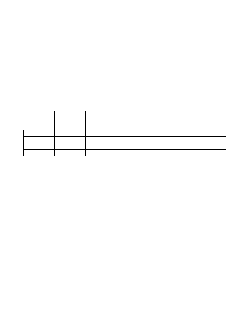
4.0 Masthead Unit (MHU)
Figure 14 is a simplified functional diagram of the Mast-Head Unit, showing the four main sub-modules:
Power conditioning
TX/RX switching
Band-pass filter
Low-Noise Amplifier (LNA)
Masthead Unit – Functional Diagram
Figure 14
4.1 Circuits and Functions
4.1.2 Power Conditioning
The dc supply for the masthead unit is routed through the command unit coaxial cable.
When the command unit is in Transmit (TX) mode, the supply voltage on the coaxial is –15 V.
When the command unit is in Receive (RX mode), the supply voltage on the coaxial is +15V.
Biasing of the low-noise amplifier (LNA) FET devices is provided by an LT1261CS, which ensures the
drain supply is switched off until the gate voltage is valid. This results in the gate voltage being
sufficiently high to keep the FET switched off during power up, thereby preventing unsaturated
operation and excessive current draw.
A comparator circuit monitors the magnitude of the gate voltage and only applies the drain when the
gate has reached approximately –1 V.
4.1.3 TX/RX Switching
The polarity of the supply voltage controls the combination of pin diode switches (MACOM MA504-30),
in the RF path.
Antenna
TX / Rx
PIN
Switch
Power
Conditioning
Tx / Rx
PIN
Switch
Band Pass
Filter
2-Stage Low- Noise
Amplifer (LNA)
CRS
Interconnect

THE BOX - Base Station Application for FCC Certification
Operating Manual
Appendix 5 Page 22 of 33
When supply voltage is +15 V (RX), the only RF path which does not appear as an open circuit
is the Low-Noise Amplifier/Band-Pass Filter. This stage is therefore able to amplify and filter the
incoming signal..
When the supply voltage is –15 V (TX), the Low-Noise Amplifier/Band-Pass Filter stage
appears as an open circuit to RF, and is therefore by-passed by the transmission signal.
4.1.4 Low-Noise Amplifier and Band-Pass Filter
4.1.4.1 Low-Noise Amplifier
The masthead unit provides the first gain stage of the receiver chain and has a very low noise and high
dynamic range characteristic.
The gain stages are provided by two Philips FET1905s. As can be seen from figure 1, a two-stage line-
up is used with the high-rejection Band-Pass Filter (BFP) between the stages.
4.1.4.2 Band-Pass Filter
The masthead receive path includes the high rejection Band-Pass Filter connected between the two
low-noise gain stages. The purpose of this filter is to remove any out-of-band spurious signal which
could give rise to inter-modulation products within the received band.
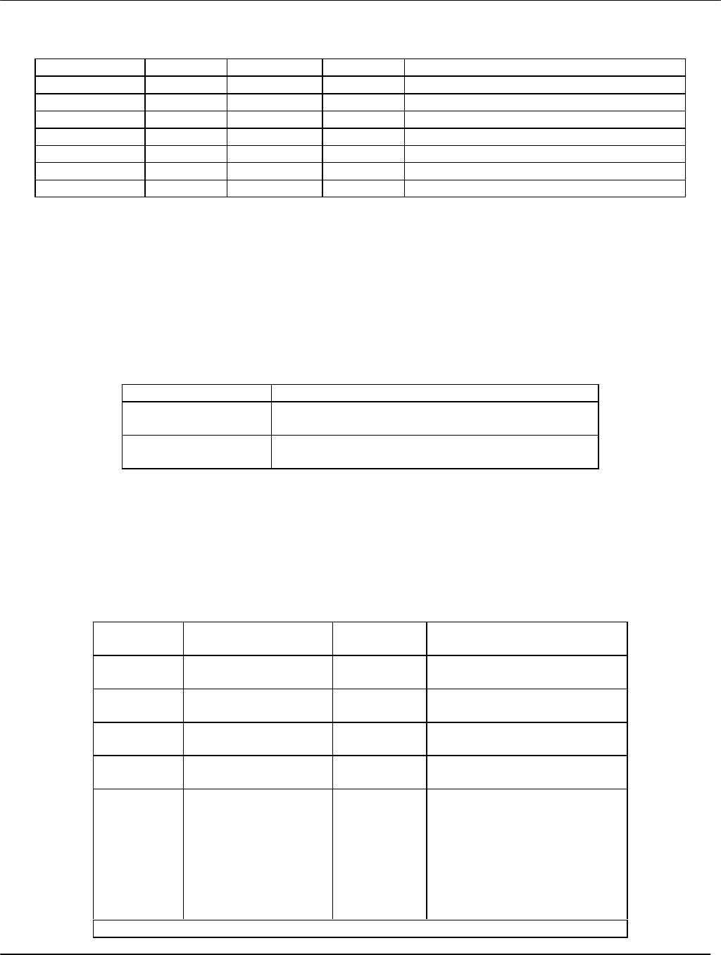
5.0 Signals & Connections
5.1 RCU
5.1.1 Connectors
External connectors to the Power Amplifier Command Transmitter are defined in table 1.
Connector
Name Description
H1 LO input - 5-way D-type Combo RF insert
H2 I & Q and data line inputs - 15-way D-type
H3 Power and RF input/output - 9-way D-type Combo RF & power inserts
H4 Power and signal lines - 9-way D-type
External Connectors
Table 1
5.1.2 Internal Interfaces
Table 2 lists the internal interface signals, which are present between the Power Amplifier and the
Linearizer sub-modules.

THE BOX - Base Station Application for FCC Certification
Operating Manual
Appendix 5 Page 23 of 33
Signal
Name From To Type Description
RF_MOD CLT PA RF Low power RF input to PA
RF_FB PA CLT RF Feed back signal for linearizer
RF_OUT PA CB RF RF power output
TX_EN LB PA Data Transmit enable
Internal Interfaces
Table 2
5.1.3 External Interfaces
Table 3 shows the signal interfaces between the Power Amplifier board and the rest of the Command
Unit.
Signal Direction Type Description
-15V In Power -15V Power supply
+28V In Power +28V Power supply to Control Board
+28V In Power +28V Power supply to PA (4.0 A)
AGND In Power Analog ground
TX_RF In/Out RF Transmitter RF output / Receiver RF input via Masthead
I_IN_AC In Analog Baseband I channel input
AGND In Power Analog ground for Linearizer board
Q_IN_AC In Analog Baseband Q channel input
SHDN In Digital Enables PA (from DSP) – used for CLT dc-nulling
5dB_UP In Digital HCMOS power control, up converter: 5dB step
5dB_DOWN In Digital HCMOS power control, down converter: 5dB step
10dB_ATT In Digital HCMOS power control: 10dB step
15dB_ATT In Digital HCMOS power control: 20dB step
PH_CTL In Analog Cartesian loop phase control
DC_NULL In Digital Cartesian loop dc null control
INSTB Out Digital Transmitter instability detector
VSWR Out Digital VSWR alarm indicator
+15V In Power +15V power for Cartesian loop
TX_RX In Digital Switches between Tx & Rx mode
TX_EN In Digital Disables the PA during a DC Null operation.
SCL In Digital Temperature sensor data clock
SDA In/Out Digital Temperature sensor bi-directional data line
RX_I_HI Out Digital Indication of masthead unit condition connection/status
RX_I_LOW Out Digital Indication of masthead unit condition connection/status
RX_RF Out RF Received RF from Tx/Rx switch
LO_TX In RF Local oscillator input 0dBm
External Interface Signals
Table 3
5.1.4 Voltage Inputs
240 V ac, 50/60 Hz or
120 V ac, 50/60 Hz
THE BOX - Base Station Application for FCC Certification
Operating Manual
Appendix 5 Page 24 of 33
5.1.5 Voltage Outputs
Dc output voltages are listed in Table 4.
Voltage
(Volts dc) Current
(Amps dc) Line Regulation
For 10% change
(%)
Load Regulation
For 10-100% change
(%)
Max
Ripple
%
+5 4< 0.2 < 0.5 < 0.5
+15 4< 0.5 < 5 < 2
-15 4< 0.5 < 5 < 2
+28 10 < 0.5 < 5 < 2
PSU Output DC Voltages
Table 4
5.2 Reference Generator & Splitter Board
5.2.1 External Connections
Table 5 lists the signals which constitute the interfaces between the Splitter Board module and the
Radio Command Unit or Data Receiver Unit.
Signal Direction Description
RF_IN In RF input signal
RF1 Out RF1 Split signal
RF2 Out RF2 Split signal
RF3 Out RF3 Split signal
AGND In Analog ground
DGND In Digital ground
+5V In Logic supply rail
40MHZ_IN In 40MHz Reference signal (DRU only)
-15V In Supply monitor input rail
+15V In RF Supply rail
+28V In Supply monitor input rail
RF4 Out RF4 Split signal
RF5 In RF5 Split signal
RF6 Out RF6 Split signal
RF7 Out RF7 Split signal
AGND In Analog ground
RF8 In RF8 Split signal
RF9 Out RF9 Split signal
RF10 Out RF10 Split signal
RF11 Out RF11 Split signal
DGND In Digital ground
+5V In Logic supply rail
-15V In Supply monitor
Continued overleaf
THE BOX - Base Station Application for FCC Certification
Operating Manual
Appendix 5 Page 25 of 33
Signal Direction Description
+15V In RF Supply rail
RF12 Out RF12 Split signal
40MHZ_REF#1 Out 40MHz Reference signal
40MHZ_REF#2 Out 40MHz Reference signal
External Interface Signals
Table 5
5.3 RF Module
5.3.1 Connectors
The connectors for the RF module are defined in Table 6.
Connector Name Description
H1 Connector to back plane -
DIN41612M 60 + 4 plugs (pins and coax inserts)
Connectors
Table 6
5.3.2 Inputs
Table 7 defines the external input signals for the RF module.
Signal Connector Type Description
+15V H1: A-C15 Power Power supply
-15V H1: A-C14 Power Power supply
+5V H1: A-C8 Power Power supply
DGND H1: A-C7 Power Digital ground
AGND H1: A-C9;A-C10;A-C12;A-C13 Power Analog ground
S_CLK H1: A-C20 HCMOS Synth. serial data clock
S_DATA H1: A-C21 HCMOS Synth. serial data
S_LE H1: A-C22 HCMOS Synth. load enable
(CU)REF H1: A-C11 RF +13dBm reference input
(DRU)REF H1: B2 RF +13dBm reference input
RX_RF H1: B31 RF Received signal input
DOE H1: A-C26 HCMOS ADC’s data output enable
FSI H1: A-C23 HCMOS ADCs frame sync input
External Inputs
Table 7
THE BOX - Base Station Application for FCC Certification
Operating Manual
Appendix 5 Page 26 of 33
5.3.3 Outputs
Table 8 defines the external output signals for the RF board.
Signal Name Connector Type Description
SDO H1: A-C24 HCMOS ADCs serial data output
SCO H1: A-C25 HCMOS ADCs serial clock output
(CU)I_RX H1: B2 Baseband Baseband I channel output
(CU)Q_RX H1: B5 Baseband Baseband Q channel output
TX_LO H1: B28 RF 0 dBm LO output CU transmitter
External Outputs
Table 8
5.3.4 Indicators
Indicators on the RF module are defined in table 9.
Indicator Name Color Description
LED1 Yellow +5V analog supply (internally generated)
LED2 Yellow +12V analog supply
LED3 Yellow -5V analog supply (internally generated)
LED4 Yellow +5V analog supply (internally generated)
LED5 Green Synthesizer Lock Detect
Indicators
Table 9
5.3.5 Internal Connections
Internal connections within the RF board are defined in table 10.
Signal Name From To Type Description
F_CLK Synth ADC Digital ADC 20.48 MHz clock
LO_+27dBm Synth RX RF Local oscillator for Command Receiver
Internal Interface Signals
Table 10
THE BOX - Base Station Application for FCC Certification
Operating Manual
Appendix 5 Page 27 of 33
5.4 Baseband Module Board
5.4.1 Power Signals
These signals are described in Table 7.
Signal Name Direction Connector Type Description
AGND In P1:A1,C1,A3,C3,A4,C4,
A6,C6
A9,B9,C9,A10,B10,C10,
A12,B12,C12,A13,B13,C
13,A27,C27,A29,C29,A3
0,C30,A32,C32
Power Analog Ground
DGND In P1:A7,B7,C7
P2:A1,B1,C1 Power Digital ground
+5V In P1:A8,B8,C8 Power Power supply
5V +/- 5%
+15V In P1:A15,B15,C15 Power Power supply
15V +/- 5%
Power Signals
Table 11
5.4.2 Analog Signals
These are described in Table 12.
Signal
Name Direction Connector Type Description
40 MHz In P1:A11,B11,C11 Analog 40 MHz Clock at +13 dBm
RX_I In P1:B2 Analog I input from receiver
2.8 V p-p into AC coupled input
RX_Q In P1:B5 Analog Q input from receiver
2.8 V p-p into AC Coupled input
TX_I Out P2:C32 Analog I output from transmitter 0.7 to 3.5 V
TX_Q Out P2:C32 Analog Q output from transmitter 0.7 to 3.5 V
Analog Signals
Table 12

THE BOX - Base Station Application for FCC Certification
Operating Manual
Appendix 5 Page 28 of 33
5.4.3 Digital Control Signals
These signals are defined in Table 13.
Signal Name Direction Connector Type Description
S_CLK Out P1: A20 HCMS Synthesizer Clock
S_DATA Out P1: A21 HCMS Synthesizer data
S_LERF Out P1: A22 HCMS RF Synthesizer enable
LOW = Enable, HIGH = DISABLE
IN#1 In P2:C2 TTL Spare input
IN#2 In P2:C3 TTL Spare input
IN#3 In P2:C4 TTL Spare input
IN#4 In P2:C5 TTL Spare input
OUT#1 Out P2:C6 HCMS Spare Output / Data Detect LED
LED Out P2:C7 TTL LED Output
20DB_ATT Out P2:C14 HCMS Transmitter 20 dB Attenuator
LOW = Switch in, HIGH = switch out
10DB_ATT Out P2:C15 HCMS Transmitter 10 dB Attenuator
LOW = Switch in, HIGH = switch out
5DB_DOWN Out P2:C16 HCMS Transmitter 5 dB Down Attenuator
LOW = Switch out, HIGH = switch in
5DB_UP Out P2:C17 HCMS Transmitter 5 dB Up Attenuator
LOW = Switch in, HIGH = switch out
T_SCL Out P2:C18 TTL Temperature sensor Clock
TX_EN Out P2:C19 HCMS Transmit enable
LOW = enable, HIGH = Disable
TX_RX Out P2:C20 HCMS Transmit/receive switch
LOW = Receive, HIGH = Transmit
RX_I_HI In P2:C21 TTL Masthead over current
LOW = Over current, HIGH = Current OK
RX_I_LO In P2:C22 TTL Masthead under current
LOW = Under current, HIGH = Current OK
T_SDA In/Out P2:C23 TTL Temperature sensor data
VSWR In P2:C24 TTL Max VSWR exceeded
(TBD - VSWR exceeded)
INSTB In P2:C25 TTL Transmitter unstable
LOW = Unstable, HIGH = not unstable
DC_NULL Out P2:C26 HCMOS Transmitter DC Null
LOW = Null, HIGH = Normal transmit
SHDN Out P2:C28 HCMOS Shut down Cartesian Loop
LOW = Disable, HIGH =enable Cartesian Loop
Digital Control Signals
Table 13
5.5 Buses
5.5.1. Radio Control Bus
The Radio Control Bus consists of an RS485 interface, and is used to control the command unit base-
band board.
The various input and output signals are described in Table 14.
THE BOX - Base Station Application for FCC Certification
Operating Manual
Appendix 5 Page 29 of 33
Signal Name Direction Connector Type Description
DID Input P1:A16 Analog Spare
DIDR Output P1:B16 Analog Spare
TZ+, TZ- Input P1:A17,B17 RS485 Message Trigger (Differential)
MS+,MS- Input P1:18,B18 RS485 Master - Slave signaling (Differential)
SM+,SM- Output P1:A19,B19 RS485 Slave - Master signaling (Differential)
Radio Control Bus
Table 14
5.5.2 Radio Data Bus
The radio data bus is used to output seismic data received over the radio link.
The inputs and outputs are differential with each path of the differential signal having TTL Logic levels.
The various signals handled by this bus are described in Table 15.
Signal Name Direction Connector
(P2) Type Description
VA0+,VA0- In A2,B2 Differential Address bit 0
VA1+,VA1- In A3,B3 Differential Address bit 1
VA2+,VA2- In A4,B4 Differential Address bit 2
VA3+,VA3- In A5,B5 Differential Address bit 3
VCLK+,VCLK- In A6,B6 Differential Clock
VRUN+,VRUN- In A7,B7 Differential Run signal
VDP+,VDP- Out A8,B8 Differential Data Present
VD0+,VD0- Out A10,B10 Differential Data bit 0
VD1+,VD1- Out A11,B11 Differential Data bit 1
VD2+,VD2- Out A12,B12 Differential Data bit 2
VD3+,VD3- Out A13,B13 Differential Data bit 3
VD4+,VD4- Out A14,B14 Differential Data bit 4
VD5+,VD5- Out A15,B15 Differential Data bit 5
VD6+,VD6- Out A16,B16 Differential Data bit 6
VD7+,VD7- Out A17,B17 Differential Data bit 7
VD8+,VD8- Out A18,B18 Differential Data bit 8
VD9+,VD9- Out A19,B19 Differential Data bit 9
VD10+,VD10- Out A20,B20 Differential Data bit 10
VD11+,VD11- Out A21,B21 Differential Data bit 11
VD12+,VD12- Out A22,B22 Differential Data bit 12
VD13+,VD13- Out A23,B23 Differential Data bit 13
VD14+,VD14- Out A24,B24 Differential Data bit 14
VD15+,VD15- Out A25,B25 Differential Data bit 15
CONN In A26 Digital Unit connected forward
RET Out B26 Digital Unit connected return
Radio Data Bus
Table 15
THE BOX - Base Station Application for FCC Certification
Operating Manual
Appendix 5 Page 30 of 33
5.5.3 RS232
Signal Name Direction Connector Type Description
GND in H4 pin 5 Power RS232 Ground
RXD Out H4 pin 2 RS232 RS232 Receive Data
TXD In H4 pin 3 RS232 RS232 Transmit Data
DTR In H4 pin 4 RS232 RS232 Data Terminal Ready
DSR Out H4 pin 6 RS232 RS232 Data Set Ready
RTS In H4 pin 7 RS232 RS232 Ready To Send
CTS Out H4 pin 8 RS232 RS232 Clear To Send
RS232 Signals
Table 16
5.6 Concentrator
5.6.1 Connectors
The connectors for the Concentrator are defined in Table 17.
Connector Name Description
H1 Connector to Data Receive Unit back plane
DIN41612 Type C (96 way male)
H2 Connector to Data Receive Unit back plane
DIN41612 Type C (96 way male)
Connectors
Table 17
5.6.2 Inputs
Table 18 defines the input signals for the Concentrator module.
Signal
Name Connector Type Description
+5V H1, pins 2a, 2b, 2c
H2, pins 2a, 2b, 2c Power Main 5V supply
+15V H1, pins 9a, 9b, 9c
H2, pins 9a, 9b, 9c Power Main +15V supply
-15V H1, pins 8a, 8b, 8c
H2, pins 8a, 8b, 8c Power Main -15V supply
DGND H1, pins 1a, 1b, 1c,
H2, pins 1a, 1b, 1c Power Digital ground
AGND H1, pins 3a, 3b, 3c
4a, 4b, 4c
6a, 6b, 6c
7a, 7b, 7c
H2, pins 3a, 3b, 3c
4a, 4b, 4c
6a, 6b, 6c
7a, 7b, 7c
Power Analog Ground
Continued Overleaf

THE BOX - Base Station Application for FCC Certification
Operating Manual
Appendix 5 Page 31 of 33
DRxD0 H1, pin 14c TTL Seismic data input bit 0
DRxD1 H1, pin 15a TTL Seismic data input bit 1
DRxD2 H1, pin 15b TTL Seismic data input bit 2
DRxD3 H1, pin 15c TTL Seismic data input bit 3
DRxD4 H1, pin 16a TTL Seismic data input bit 4
DRxD5 H1, pin 16b TTL Seismic data input bit 5
DRxD6 H1, pin 16c TTL Seismic data input bit 6
DRxD7 H1, pin 17a TTL Seismic data input bit 7
DRxD8 H1, pin 17b TTL Seismic data input bit 8
DRxD9 H1, pin 17c TTL Seismic data input bit 9
DRxD10 H1, pin 18a TTL Seismic data input bit 10
DRxD11 H1, pin 18b TTL Seismic data input bit 11
DRxD12 H1, pin 18c TTL Seismic data input bit 12
DRxD13 H1, pin 19a TTL Seismic data input bit 13
DRxD14 H1, pin 19b TTL Seismic data input bit 14
DRxD15 H1, pin 19c TTL Seismic data input bit 15
DRxP H1, pin 13b TTL Data Rx present
High: Card fitted
Low: Card not fitted
DRxDP H1, pin 13c TTL Data Rx data available
High: Data available
Low: Data not available
DRxO H1, pin 14a TTL Data Rx data o/p buffer
overflow1
High: Buffer overflow
Low : Buffer OK
40MHz In H1, 5a, 5b, 5c Analog 40.0MHz clock at +13 dBm
VA0+ H2, pin 10a Differential RDB Rack address bit 0
VA0- H2, pin 10b Differential RDB Rack address bit 0
VA1+ H2, pin 11a Differential RDB Rack address bit 1
VA1- H2, pin 11b Differential RDB Rack address bit 1
VA2+ H2, pin 12a Differential RDB Rack address bit 2
VA2- H2, pin 12b Differential RDB Rack address bit 2
VA3+ H2, pin 13a Differential RDB Rack address bit 3
VA3- H2, pin 13b Differential RDB Rack address bit 3
VClk+ H2, pin 14a Differential RDB I/F data clock
Data is clocked into recording
computer on rising edge.
VClk- H2, pin 14b Differential RDB I/F data clock
VRun+ H2, pin 15a Differential RDB I/F Run control
High: During data transfers
Low: Otherwise
VRun- H2, pin 15b Differential RDB I/F Run control
Vreset+ H2, pin 17a Differential Concentrator reset
Vreset- H2, pin 17b Differential Concentrator reset
/DRxRdy H1, pin 14b TTL Data receiver ready for DMA
data transfer
Low: ready, High: Not ready
BIB_EN H1, pin 20a TTL Enable RCB slave master
output, wire-or from DRUs
Active Low
External Input Table 18

THE BOX - Base Station Application for FCC Certification
Operating Manual
Appendix 5 Page 32 of 33
5.6.3 Outputs
Table 19 defines the output signals for the Concentrator board.
Signal Name Connector Type Description
VDP+ H2, pin 16a Differential Data present flag
High: Data available for reading
Low: No data available
VDP- H2, pin 16b Differential Data available flag
VD0+ H2, pin 18a Differential RDB Data bit 0
VD0- H2, pin 18b Differential RDB Data bit 0
VD1+ H2, pin 19a Differential RDB Data bit 1
VD1- H2, pin 19b Differential RDB Data bit 1
VD2+ H2, pin 20a Differential RDB Data bit 2
VD2- H2, pin 21a Differential RDB Data bit 2
VD3+ H2, pin 22a Differential RDB Data bit 3
VD3- H2, pin 23a Differential RDB Data bit 3
VD4+ H2, pin 24a Differential RDB Data bit 4
VD4- H2, pin 24b Differential RDB Data bit 4
VD5+ H2, pin 25a Differential RDB Data bit 5
VD5- H2, pin 25b Differential RDB Data bit 5
VD6+ H2, pin 26a Differential RDB Data bit 6
VD6- H2, pin 26b Differential RDB Data bit 6
VD7+ H2, pin 25c Differential RDB Data bit 7
VD7- H2, pin 26c Differential RDB Data bit 7
VD8+ H2, pin 27a Differential RDB Data bit 8
VD8- H2, pin 27b Differential RDB Data bit 8
VD9- H2, pin 28b Differential RDB Data bit 9
VD10+ H2, pin 27c Differential RDB Data bit 10
VD10- H2, pin 28c Differential RDB Data bit 10
VD11+ H2, pin 29a Differential RDB Data bit 11
VD11- H2, pin 29b Differential RDB Data bit 11
VD12+ H2, pin 30a Differential RDB Data bit 12
VD12- H2, pin 30b Differential RDB Data bit 12
VD13+ H2, pin 29c Differential RDB Data bit 13
VD13- H2, pin 29d Differential RDB Data bit 13
VD14+ H2, pin 31a Differential RDB Data bit 14
VD14- H2, pin 31b Differential RDB Data bit 14
VD15+ H2, pin 32a Differential RDB Data bit 15
VD15- H2, pin 32b Differential RDB Data bit 15
/DRxReq H1, pin 10a TTL Data Receiver DMA request
Low: Request
High: No request
DRxClk H1, pin 10b TTL Clocks data out of the buffer on Data
RF board on rising edge and into
FIFO on the falling edge.
DRxA0 H1, pin 10c TTL Address line 0 for channel data
DRxA1 H1, pin 11a TTL Address line 1 for channel data
DRxA2 H1, pin 11b TTL Address line 2 for channel data
DRxA3 H1, pin 11c TTL Address line 3 for channel data
DRxA4 H1, pin 12a TTL Address line 4 for channel data
Continued Overleaf
THE BOX - Base Station Application for FCC Certification
Operating Manual
Appendix 5 Page 33 of 33
DRxA5 H1, pin 12b TTL Address line 5 for channel data
DRxA6 H1, pin 12c TTL Address line 6 for channel data
DRxA7 H1, pin 13a TTL Address line 7 for channel data
External Outputs
Table 19
5.6.4 Bi-directional Signals
Table 20 lists the external bi-directional interface signals for the Concentrator.
Signal
Name Connector Description
SM#1+ H1 pin 31a To SMU ( SM2 buffered from DRUs)
SM#1- H1 pin 31b To SMU ( SM2 buffered from DRUs)
MS#1+ H1 pin 30a From SMU, (buffer to DRUs)
MS#1- H1 pin 30b From SMU, (buffer to DRUs)
SM#2+ H1 pin 20b From DRUs (buffer to SMU)
SM#2- H1 pin 20c From DRUs (buffer to SMU)
MS#2+ H1 pin 21b To DRUs (MS1 buffered from SMU)
MS#2- H1 pin 21c To DRUs (MS1 buffered from SMU)
SM#3+ H2 pin 21b Termination input for SM2
SM#3- H2 pin 20c Termination input for SM2
MS#3+ H2 pin 21b Termination input for MS2
MS#3- H2 pin 21c Termination input for MS2
External Bi-Directional RCB Interface Signals
Table 20
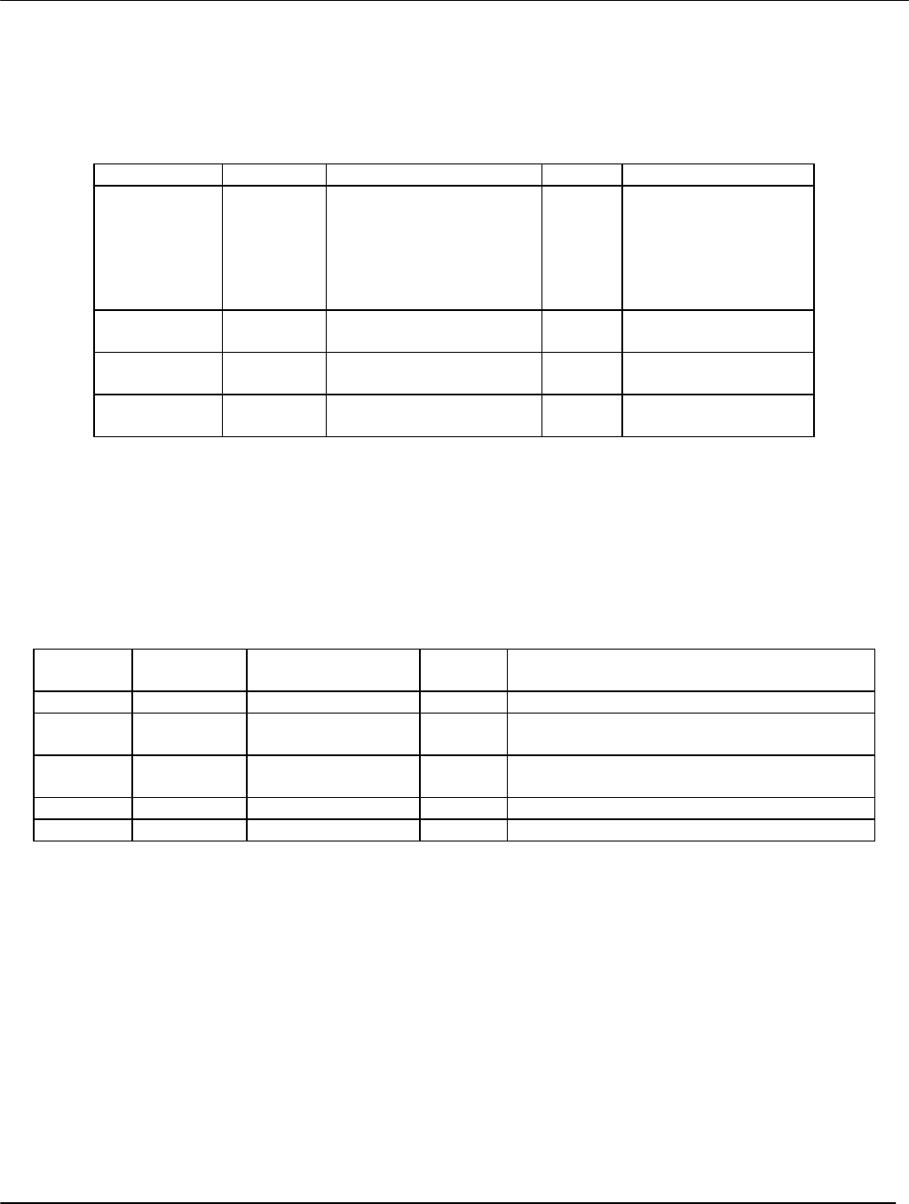
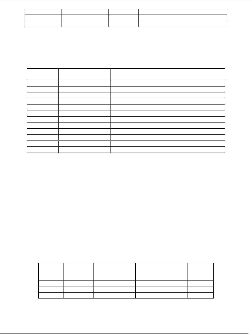
5.7 Power Supply Module
5.7.1 Inputs
240 V ac, 50/60 Hz or
120 V ac, 50/60 Hz.
5.7.2 Outputs
DC output voltages are summarized in Table 21.
Voltage
(V dc) Current
(A dc) Line Regulation
For 10% change
(%)
Load Regulation
For 10-100% change
(%)
Max
Ripple
%
+ 5 50 < 0.2 < 0.5 < 0.5
+15 8< 0.5 < 10.0 < 2.0
-15 8< 0.5 < 10.0 < 2.0
PSU Output Voltages
Table 2