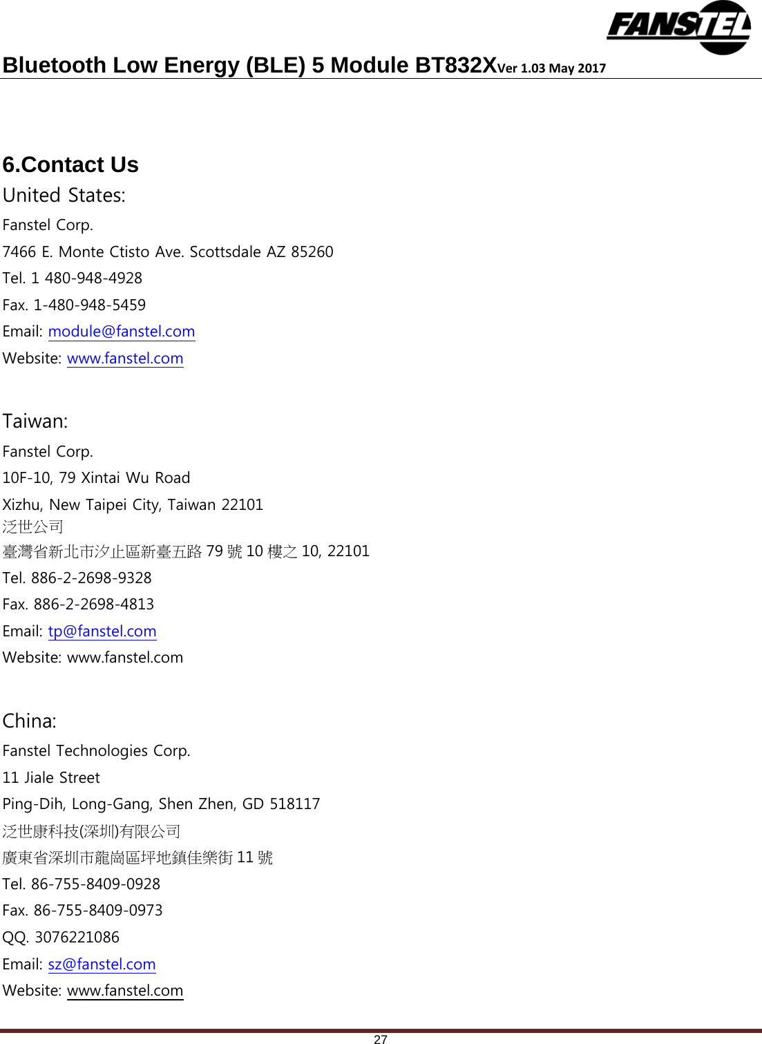
Fanstel Taipei BT832X Bluetooth 5Module User Manual BlueNor BT832X datasheetsx
Fanstel Corporation, Taipei Bluetooth 5Module BlueNor BT832X datasheetsx
UserManual.wiki
>
Fanstel Taipei
>
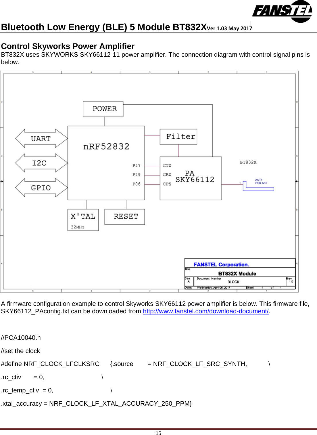
BT832X User Manual
Users Manual
Navigation menu
Upload a User Manual
Namespaces
Wiki Guide
HTML
PDF
Info
Views
User Manual
Discussion / Help
Navigation