Fanstel Taipei BT840 Bluetooth 5.0 Module User Manual
Fanstel Corporation, Taipei Bluetooth 5.0 Module Users Manual
Users Manual
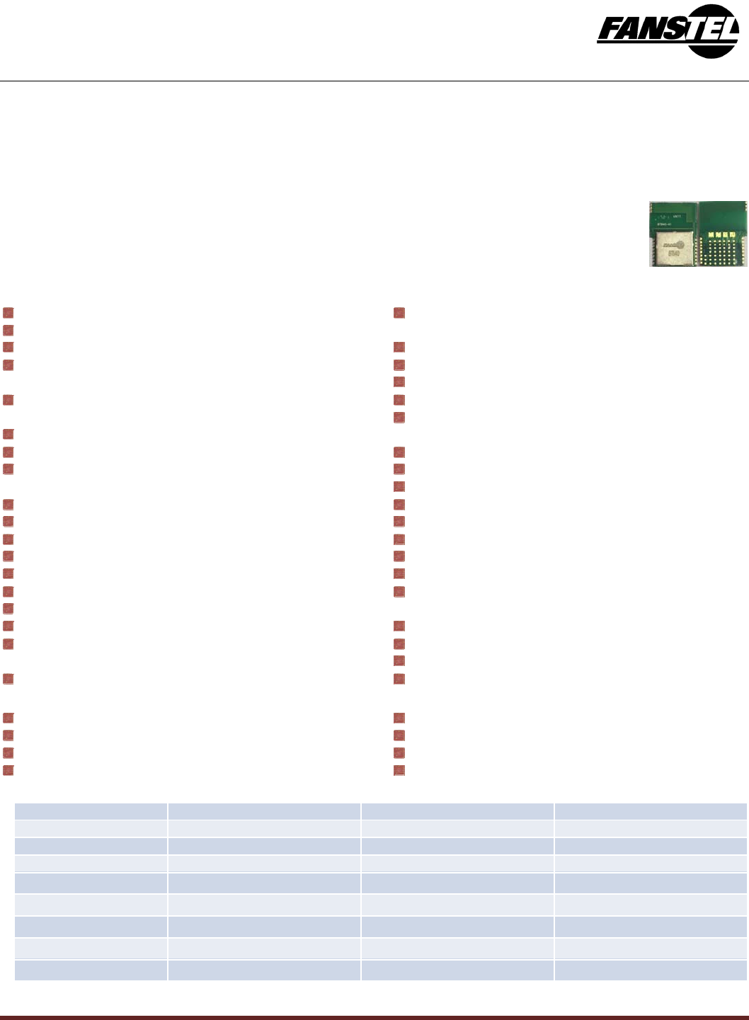
Bluetooth Low Energy(BLE) 5 Module BT840FVer 0.91 Nov. 2017 draft
1
BluNor BT840F is a powerful, highly flexible, ultra low power Bluetooth Low Energy (BLE) using Nordic
nRF52840 SoC. With an ARMCortexTM M4F MCU, available 1MB flash, 256KB RAM, embedded 2.4GHz multi-
protocol transceiver, and an integrated PCB trace antenna or u.FL connector for an external +6dBi antenna. It
allows faster time to market with reduced development cost.
For applications needing limited number of IO pins, prototyping and production are easier
using 16 castellated pins. Additional 45 LGA (Land Grid Array) pins provide full access to 48
GPIOs of nRF52840.
BT840F hasan ARM® TrustZone® CryptoCell-310co-processor for implementation of IoT security.
Specifications:
Nordic nRF52840 with ARM Cortex M4F, 64 MHz
ARM® TrustZone® Cryptocell-310 co-processor
Complete RF solution with integrated antenna
Bluetooth 5 data rate: 2Mbps, 1Mbps, 500kbps,
125kbps.
IEEE 802.15.4 Thread and Zigbee data rate: 250
Kbps
2.4 GHz proprietary data rate: 2 Mbps, 1 Mbps
Integrated DC-DC converter, inductors on board.
Direct powered by Lithium batteries or USB supply
(up to 5.5V)
Serial Wire Debug (SWD)
Nordic SoftDevice Ready
Over-the-Air (OTA) firmware update
Flash/RAM: 1MB/256KB.
48 General purpose I/O pins
USB 2.0 full speed (12 Mbps) controller
QSPI 32 MHz interface
High speed 32 MHz SPI
Type 2 NFC-A tag with wake-on field, Touch-to-pair
support
Programmable peripheral interconnect (PPI)
12 bit/200 Ksps ADC, 8 configurable channels with
programmable gain
64 level comparator
15 level comparator with wake-up from OFF mode
Temperature sensor
4x4-channel pulse width modulator (PWM)
Audio peripherals: I2S, digital microphone interface
(PDM)
5 x 32 bit timers with counter mode
Up to 4x SPI masters/3x SPI slaves
Up to 2x I2C compatible 2-wire masters/slaves
2x UART (CTS/RTS)
Quadrature Demodulator (QDEC)
3x real time counters (RTC)
128-bit AES HW encryption
SoC Receiver Sensitivity: -96 dBm at 1Mbps
SoC TX power: programmable +8dBm to -20dBm.
Up to +6 dBi antenna gain.
Hybrid pins: 16 castellated and 45 LGA.
Integrated PCB trace antenna or u.FL connector
Operation voltage: 1.7V to 5.5V
Operation temperature: - 4 0 ° C t o + 8 5 ° C
Applications
Secure IoT
Wearable
Beacons/Proximity
Connected appliances
Lighting products
Sensors
Home and building automation
Wrist watches
Model Summaries
module BT840F BT840 BT840E
SoC nRF52840-QIAA nRF52840-QIAA nRF52840-QIAA
Size 15x20.8x1.9mm 14x16x1.9mm 14x16x1.9mm
BT Antenna PCB trace PCB trace u.FL
BT range at 1Mbps 510 meters 180 M, estimated
BT range at 125 Kbps 930 meters >1000 M
FCC ID
Canada IC ID
Europe

Bluetooth Low Energy(BLE) 5 Module BT840FVer 0.91 Nov. 2017 draft
2
Table Of Contents
1. Introduction .......................................................................................................................................................... 3
BT840F Block Diagram ........................................................................................................................................ 3
BT840F ................................................................................................................................................................. 3
BT840 ................................................................................................................................................................... 4
BT840E ................................................................................................................................................................ 4
2. Codes Development Using Nordic Tools ............................................................................................................ 5
Easy, fast and safe code development ............................................................................................................... 5
Over-The-Air DFU ................................................................................................................................................ 5
SoftDevices .......................................................................................................................................................... 5
Development Tools .............................................................................................................................................. 5
3. Product Descriptions ............................................................................................................................................ 6
Block Diagram of nRF52840 ................................................................................................................................ 6
ARM Trustzone CryptoCell 310 ........................................................................................................................... 8
Mechanical Drawings ......................................................................................................................................... 10
Pin Assignments of BT840 ................................................................................................................................ 11
Pin Function ....................................................................................................................................................... 14
Mounting BT840F on the Host PCB .................................................................................................................. 15
Host Board Design for Low Cost or Long Range .............................................................................................. 16
4. BT840F Evaluation Board ................................................................................................................................. 17
Communicating with a PC ................................................................................................................................. 17
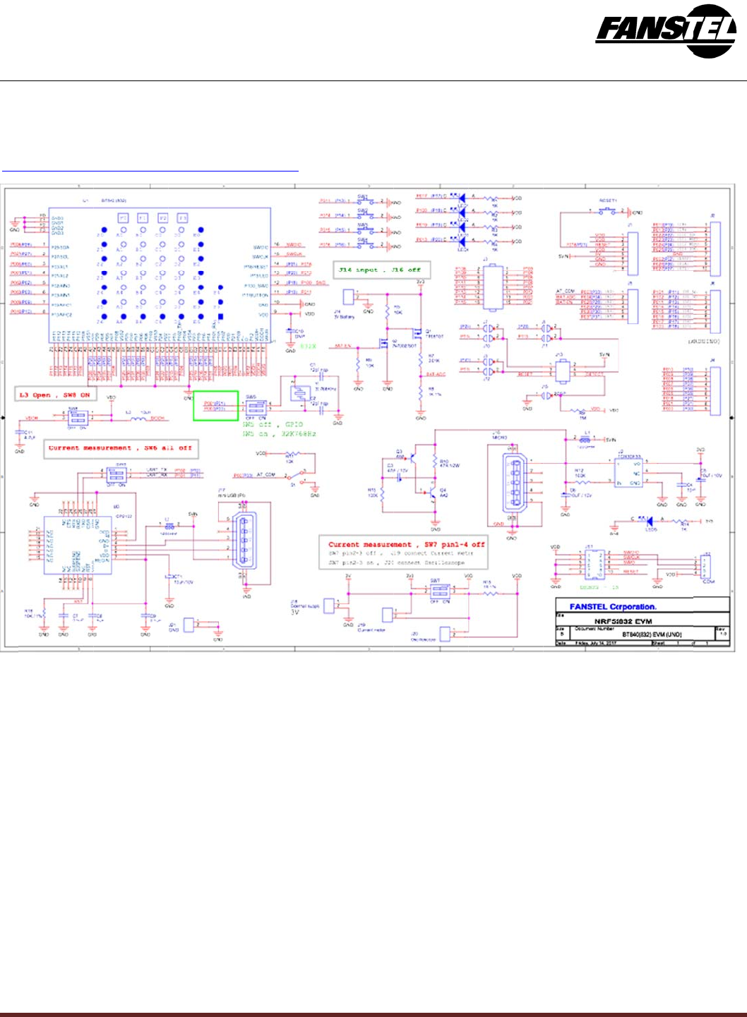
EV BT840F V4 EvaluationBoard Schematics ................................................................................................... 18
Suggestion for Battery Power Application ......................................................................................................... 19
5. Miscellaneous .................................................................................................................................................... 20
Soldering Temperature-Time Profile for Re-Flow Soldering ............................................................................. 20
Cautions, Design Notes, and Installation Notes ................................................................................................ 20
Packaging ........................................................................................................................................................... 23
FCC Label .......................................................................................................................................................... 23
6. Contact Us ......................................................................................................................... 錯誤! 尚未定義書籤。
Bluetooth Low Energy(BLE) 5 Module BT840FVer 0.91 Nov. 2017 draft
3
1. Introduction
BluNor BT840F Series are powerful, highly flexible, ultra low power wireless modules using Nordic nRF52840
SoCs. With an ARMCortexTM M4F MCU, 1MB flash, 256KB RAM, embedded 2.4GHz multi-protocol
transceiver, and an integrated antenna, it allows faster time to market with reduced development cost.
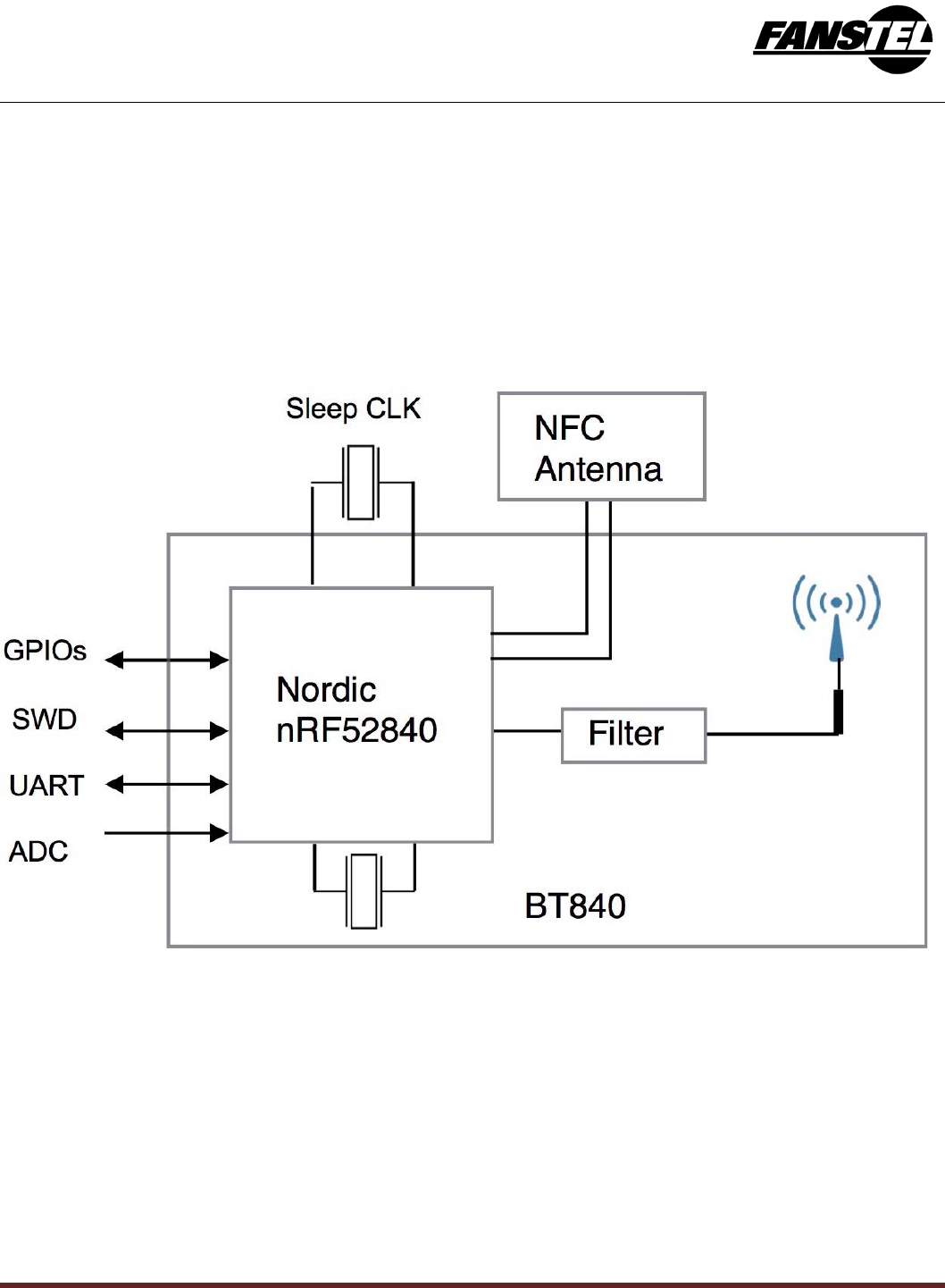
The following is a block diagram of BT840F. Antenna circuit and main clock are integrated. All 48 GPIOs of
nRF52840 can be accessed from main board. For lower power consumption at idle state, a 32.768 kHz crystal
can be added on the host board. Connection to an external NFC (Near Field Communication) antenna is
provided.
BT840F Block Diagram
BlurNor BT840F is a sister module of BT832F. The physical size is the same. There are 21 additional LGA pins
for additional GPIOs provided by nRF52840.
There are 3 modules in the BT840F Series.
BT840F
• Uses an nRF52840 QIAA with Cortex M4F MCU
• 1MB flash, 256 KB RAM

Bluetooth Low Energy(BLE) 5 Module BT840FVer 0.91 Nov. 2017 draft
4
• Supports NFC
• Integrated PCB trace range antenna. Bluetooth range is 510 meters at 1Mbps and 930 meters at 125 Kbps.
• Size: 15x20.8x1.9mm.
BT840
• Uses an nRF52840 QIAA with Cortex M4F MCU
• 1MB flash, 256 KB RAM
• Supports NFC
• Integrated PCB trace range antenna. Bluetooth range is estimated at 180 meters at 1Mbps.
• Size: 14x16x1.9mm.
BT840E
• Uses an nRF52840 QIAA with Cortex M4F MCU
• 1MB flash, 256 KB RAM
• Supports NFC
• An u.FL connector for external antenna. Bluetooth range is estimated at over 1000 meters at 125 Kbps with
ANT060 external antenna.
• Size: 14x16x1.9mm.

Bluetooth Low Energy(BLE) 5 Module BT840FVer 0.91 Nov. 2017 draft
5
2. Codes Development Using Nordic Tools
Development tools by Nordic and other third party development tools recommended by Nordic should be
used .
Easy, fast and safe code development
Nordic development environment for nRF52840
offers a clean separation between application code development and embedded protocol stacks. This means
compile, link and run time dependencies with the embedded stack and associated debugging challenges are
removed. The Bluetooth low energy and ANT stack is a pre-compiled binary, leaving application code to be
compiled stand-alone. The embedded stack interface uses an asynchronous and event driven model removing
the need for RTOS frameworks.
Over-The-Air DFU
The nRF52840 is supported by an Over-The-Air Device Firmware Upgrade (OTA DFU) feature. This allows for
in the field updates of application software and SoftDevice.
SoftDevices
The Nordic protocol stacks are known as SoftDevices and complement the nRF52 Series SoCs. All nRF52 Series are
programmable with software stacks from Nordic. This bring maximum flexibility to application development and allows
the latest stack version to be programmed into the SoC.
SoftDevices available from Nordic:
S140: Bluetooth low energy concurrent central/peripheral/observer/broadcaster stack.
Development Tools
Nordic Semiconductor provides a complete range of hardware and software development tools for the nRF52 Series
devices. nRF52 DK board is recommended for firmware development.
Nordic software development tools can be downloaded from the following webpage.
http://infocenter.nordicsemi.com/index.jsp?topic=/com.nordic.infocenter.nrf52/dita/nrf52/development/nrf52_dev_kit.htm
l&cp=1_1

Bluetooth Low Energy(BLE) 5 Module BT840FVer 0.91 Nov. 2017 draft
6
3. Product Descriptions
Brief description of nRF52840 SoC is provided. For full description of the SoC, please download from Nordic
Semiconductor website.
https://www.nordicsemi.com/eng/Products/Bluetooth-low-energy
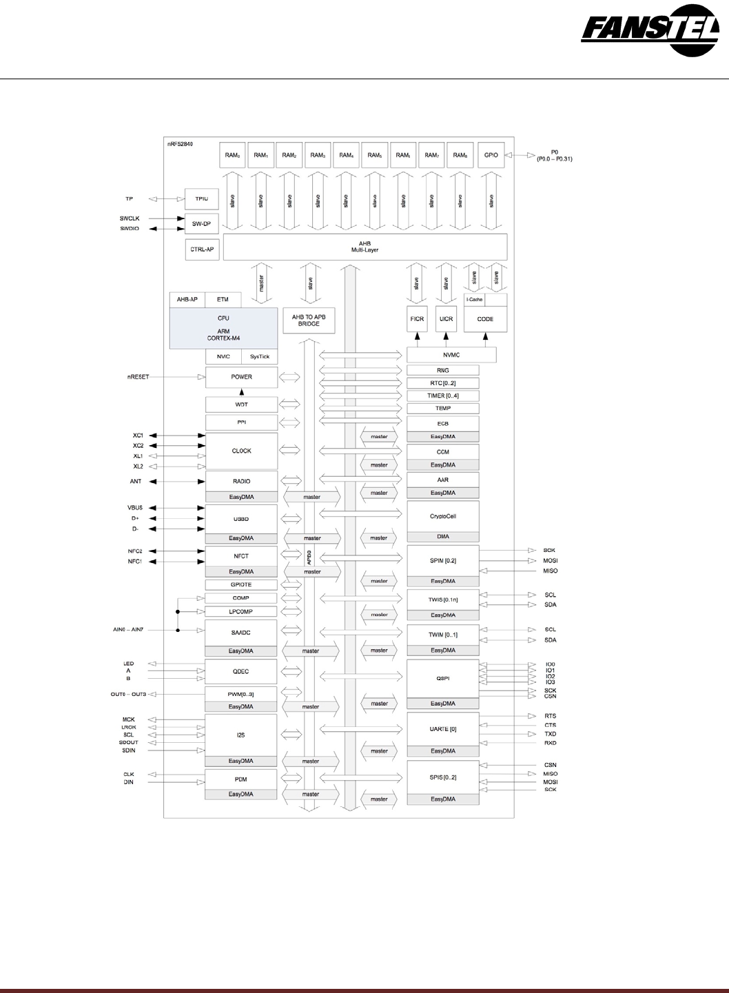
Block Diagram of nRF52840
Bluetooth Low Energy(BLE) 5 Module BT840FVer 0.91 Nov. 2017 draft
7
The following is a block diagram of Nordic nRF52840 Bluetooth Low Energy (BLE) SoC. Arrows with white
heads indicate signals that share physical pins with other signals.
The 32 bit ARM Cortex M4F MCU with hardware supports for DSP instructions and floating point operations,
code density and execution speed are higher than other Cortex M MCU. The Programmable Peripheral
Interconnect (PPI) system provides a 20-channel bus for direct and autonomous system peripheral
communication without CPU intervention. This brings predictable latency times for peripheral to peripheral
interaction and power saving benefits associated with leaving CPU idle. The device has 2 global power modes
Bluetooth Low Energy(BLE) 5 Module BT840FVer 0.91 Nov. 2017 draft
8
ON/OFF, but all system blocks and peripherals have individual power management control which allows for an
automatic switching RUN/IDLE for system blocks based only on those required/not required to achieve
particular tasks.
The radio supports Bluetooth low energy and ANT. Output power is scalable from a maximum of +8dBm down
to -20 dBm in 4dB steps. Sensitivity is increased to -96 dBm to -89 dBm, depending on data rate. Sensitivity for
BLE is -96 dBm, and -92.5 dBm for ANT.
The NFC block supports NFC-A tags with proximity detection and Wake-on-field from low power mode. The
NFC enables Out-Of-Band (OOB) Bluetooth pairing of devices and thus greatly simplifying deployment.
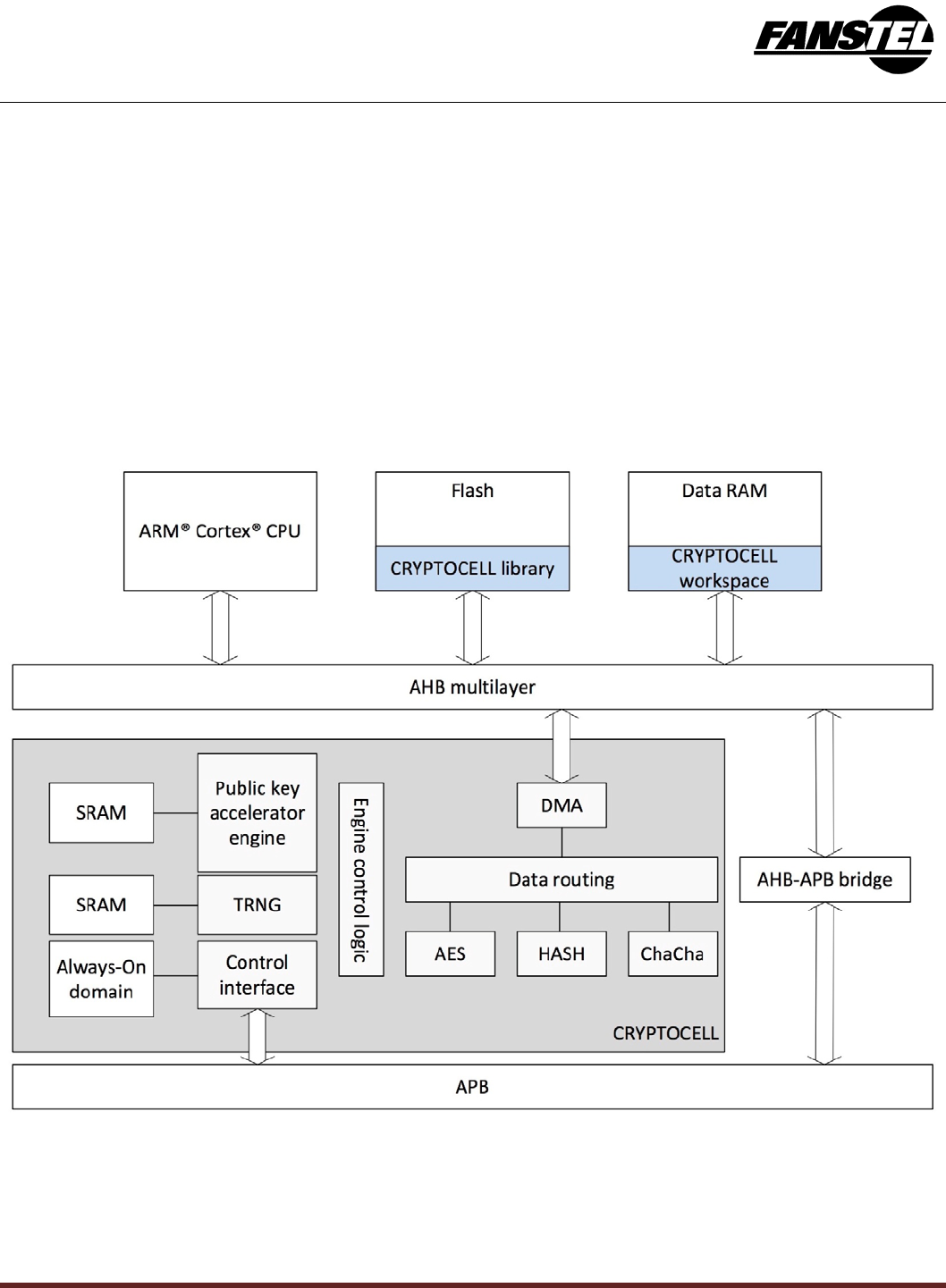
ARM Trustzone CryptoCell 310
ARM® TrustZone® CryptoCell-310co-processor is a security subsystem which provides Root of Trust (RoT) and
cryptographic services for a device. CryptoCell services are available to the application through a software library API, not
a hardware register interface.
The following cryptographic features are provided.
• FIPS-140-2 certified True Random Number Generator (TRNG)

Bluetooth Low Energy(BLE) 5 Module BT840FVer 0.91 Nov. 2017 draft
9
• RSA asymmetric encryption
Up to 2048 bit key size
PKCS#1 v2.1/v1.5
Optional CRT support
• Elliptic curve cryptography (ECC)
NIST FIPS 186-4 recommended curves using pseudo-random parameters, up to 521 bits:
➢ Prime field: P-192, P-224, P-256, P-384, P-521
SEC 2 recommended curves using pseudo-random parameters, up to 521 bits:
➢ Prime field: P-160, P-192, P-224, P-256, P-384, P-521
Koblitz curves using fixed parameters, up to 256 bits:
➢ Prime field: P-160, P-192, P-224, P-256
Edwards/Montgomery curves:
➢ Ed25519, Curve 25519
ECDH/ECDSA support
• Secure remote password protocol (SRP)
Up to 3072 bit operations
• Hashing functions
SHA-1, SHA-2 up to 256 bit size
keyed-hash message authentication code (HMAC)
• AES symmetric encryption
General purpose AES engine (encrypt/decrypt, sign/verify)
128 bit key size
Supported encryption modes: ECB, CBC, CMAC/CBC-MAC, CTR, CCM/CCM*.
• ChaCha20/Poly1305 symmetric encryption
Supported keyed size: 128 and 256 bits
Authenticated encryption with associated data (AEAD) mode
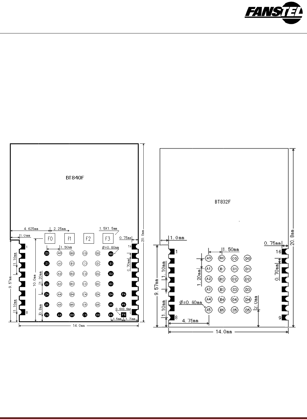
B
M
T
h
15
Fi
r
T
w
B
T
luetoot
h
echanic
a
h
e following
s
x20.8x1.9
m
r
mware con
w
o types of
p
• 16 ca
s
solde
r
• 45 L
G
T
840F and
B
h
Low
E
a
l Drawi
n
s
are mech
a
m
m. Except
figuration i
s
p
ins are av
a
s
tellated pi
n
r
ing castell
a
G
A (Land G
r
B
T832F Me
E
nergy(
n
gs
a
nical draw
i
the 19 pins
s
required t
o
a
ilable to m
e
n
s for appli
c
a
ted pins.
r
id Array) pi
chanical dr
a
BLE) 5
i
ngs of BT8
in solid bla
c
o
perform t
h
eet differen
c
ation need
i
ns to acce
s
a
wings, top
Modul
e
10
40F and B
T
c
k dots, BT
h
e same fu
n
t applicatio
n
i
ng limited
n
s
s all 48 GP
view
e
BT840
T
832F. The
840F and
B
n
ction.
n
requirem
e
n
umber of I
O
IOs of nRF
5
F
Ver 0.91
N
physical si
z
B
T832F is h
a
e
nts.
O
s. SMT e
q
5
2840 whe
n
N
ov. 2017 d
r
z
es of both
a
rdware pi
n
q
uipment is
n
needed.
r
aft
are the sa
m
n
to pin co
m
not require
d
m
e,
m
patible.
d
for
Bluetooth Low Energy(BLE) 5 Module BT840FVer 0.91 Nov. 2017 draft
11
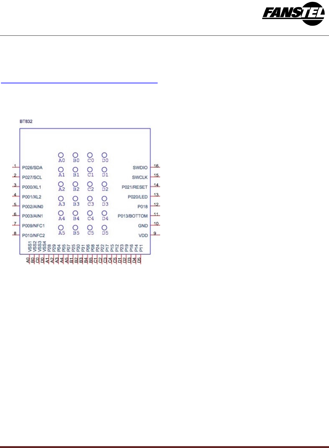
Pin Assignments of BT840
The followings are BT840 pin assignment. Pin functions are in a table in next section. Please refer to Nordic
nRF52840 Product Specifications for detailed descriptions and features supported.
https://www.nordicsemi.com/eng/Products/nRF52840
BT840F pins is a super set of that of BT832F. A PCB developed for BT832 Series can be used for BT840
Series and vice versa.
BT832F pin assignments.
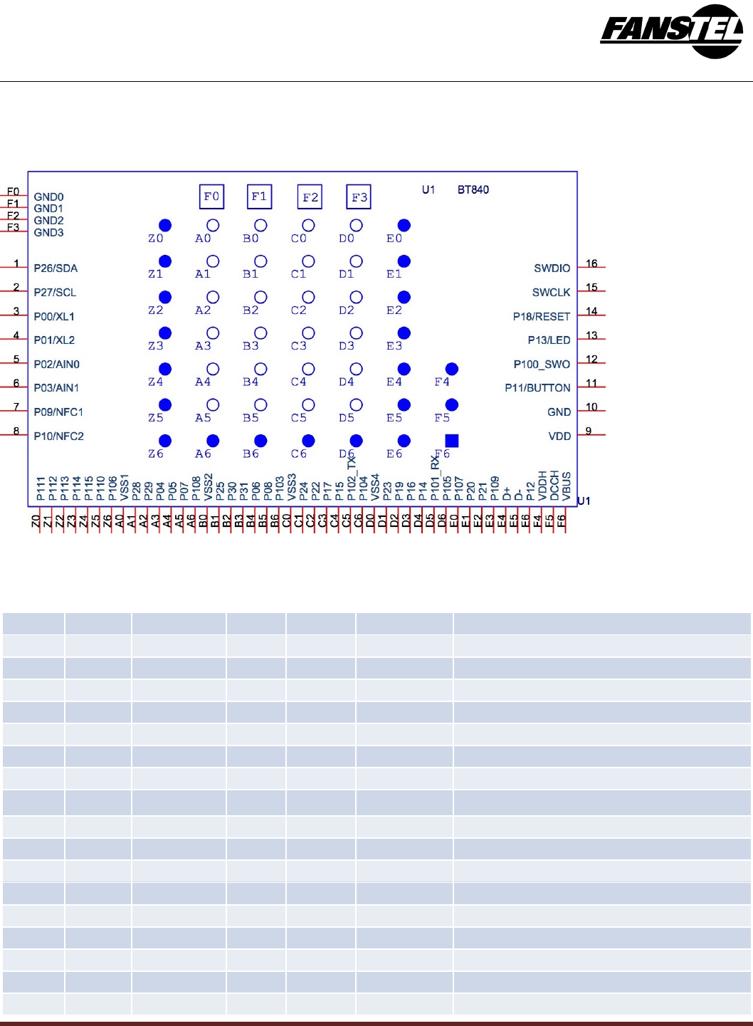
Bluetooth Low Energy(BLE) 5 Module BT840FVer 0.91 Nov. 2017 draft
12
BT840F pin assignments
BT840 52840 BT832 52832
pin# pin# pin name pin# pin# pin name Descriptions
1 G1 P0.26/SDA 1 38 P0.26 GPIO, configured as I2C SDA on EV-BT840
2 H2 P0.27/SCL 2 39 P0.27 GPIO, configured as I2C SCL on EV-BT840
3 D2 P0.00/XL1 3 2P0.00/XL1 GPIO, connection for 32.768kHz crystal
4 F2 P0.01/XL2 4 3P0.01/XL2 GPIO, connection for 32.768kHz crystal
5 A12 P0.02/AIN0 5 4P0.02/AIN0 GPIO, Analog input
6 B13 P0.03/AIN1 6 5P0.03/AIN1 GPIO, Analog input
7 L24 P0.09/NFC1 7 11 P0.09/NFC1 GPIO, NFC antenna connection
8 J24 P0.10/NFC2 8 12 P0.10/NFC2 GPIO, NFC antenna connection
9 B1 VDD 9 13 VDD DC supply 1.7V to 3.6V
10 B7 GND 10 45 VSS Ground
11 T2 P0.11 11 16 P0.13 GPIO
12 AD22 P1.00 12 21 P0.18 GPIO
13 AD8 P0.13 13 23 P0.20 GPIO
14 AC13 P0.18/RESET 14 24 P0.21/RESET GPIO, configurable as RESET pin
15 AA24 SWDCLK 15 25 SWDCLK Serial Wire Debug clock input
16 AC24 SWDIO 16 26 SWDIO Serial Wire Debug I/O

Bluetooth Low Energy(BLE) 5 Module BT840FVer 0.91 Nov. 2017 draft
13
Z0 B19 P1.11 GPIO
Z1 B17 P1.12 GPIO
Z2 A16 P1.13 GPIO
Z3 B15 P1.14 GPIO
Z4 A14 P1.15 GPIO
Z5 A20 P1.10 GPIO
Z6 R24 P1.06 GPIO
A0 GND A0 45 VSS Ground
A1 B11 P0.28/AIN4 A1 40 P0.28/AIN4 GPIO, Analog input
A2 A10 P0.29/AIN5 A2 41 P0.29/AIN5 GPIO, Analog input
A3 J1 P0.04/AIN2 A3 6P0.04/AIN2 GPIO, Analog input
A4 K2 P0.05/AIN3 A4 7P0.05/AIN3 GPIO, Analog input
A5 M2 P0.07 A5 9P0.07 GPIO
A6 P2 P1.08 GPIO
B0 GND B0 45 VSS Ground
B1 AC21 P0.25 B1 37 P0.25 GPIO
B2 B9 P0.30/AIN6 B2 42 P0.30 GPIO
B3 A8 P0.31/AIN7 B3 43 P0.31 GPIO
B4 L1 P0.06 B4 8P0.06 GPIO, NC for BT832X, BT840X, PA conrol
B5 N1 P0.08 B5 10 P0.08 GPIO
B6 V23 P1.03 GPIO
C0 GND C0 45 VSS Ground
C1 AD20 P0.24 C1 29 P0.24 GPIO
C2 AD18 P0.22 C2 27 P0.22 GPIO
C3 AD12 P0.17 C3 20 P0.17 GPIO, NC for BT832X,BT840X, PA control
C4 AD10 P0.15 C4 18 P0.15 GPIO
C5 W24 P1.02 C5 15 P0.12 GPIO
C6 U24 P1.04 GPIO
D0 GND D0 45 VSS Ground
D1 AC19 P0.23 D1 28 P0.23 GPIO
D2 AC15 P0.19 D2 22 P0.19 GPIO, NC for BT832X,BT840X, PA control
D3 AC11 P0.16 D3 19 P0.16 GPIO
D4 AC9 P0.14 D4 17 P0.14 GPIO
D5 Y23 P1.01 D5 14 P0.11 GPIO
D6 T23 P1.05 GPIO
E0 P23 P1.07 GPIO
E1 AD16 P0.20 GPIO
E2 AC17 P0.21 GPIO
E3 R1 P1.09 GPIO
E4 AD6 D+ USB D+

Bluetooth Low Energy(BLE) 5 Module BT840FVer 0.91 Nov. 2017 draft
14
E5 AD4 D- USB D-
E6 U1 P0.12 GPIO
F0 Ground pad, for BT840F V1, BT832X, BT840X
F1 Ground pad, for BT840F V1, BT832X, BT840X
F2 Ground pad, for BT840F V1, BT832X, BT840X
F3 Ground pad, for BT840F V1, BT832X, BT840X
F4 Y2 VDDH High Voltage Power Supply
F5 AB2 DCCH DC to DC converter output
F6 AD2 VBUS 5V DC power for USB 3.3V regulator
Pin Function
Bluetooth Low Energy(BLE) 5 Module BT840FVer 0.91 Nov. 2017 draft
15
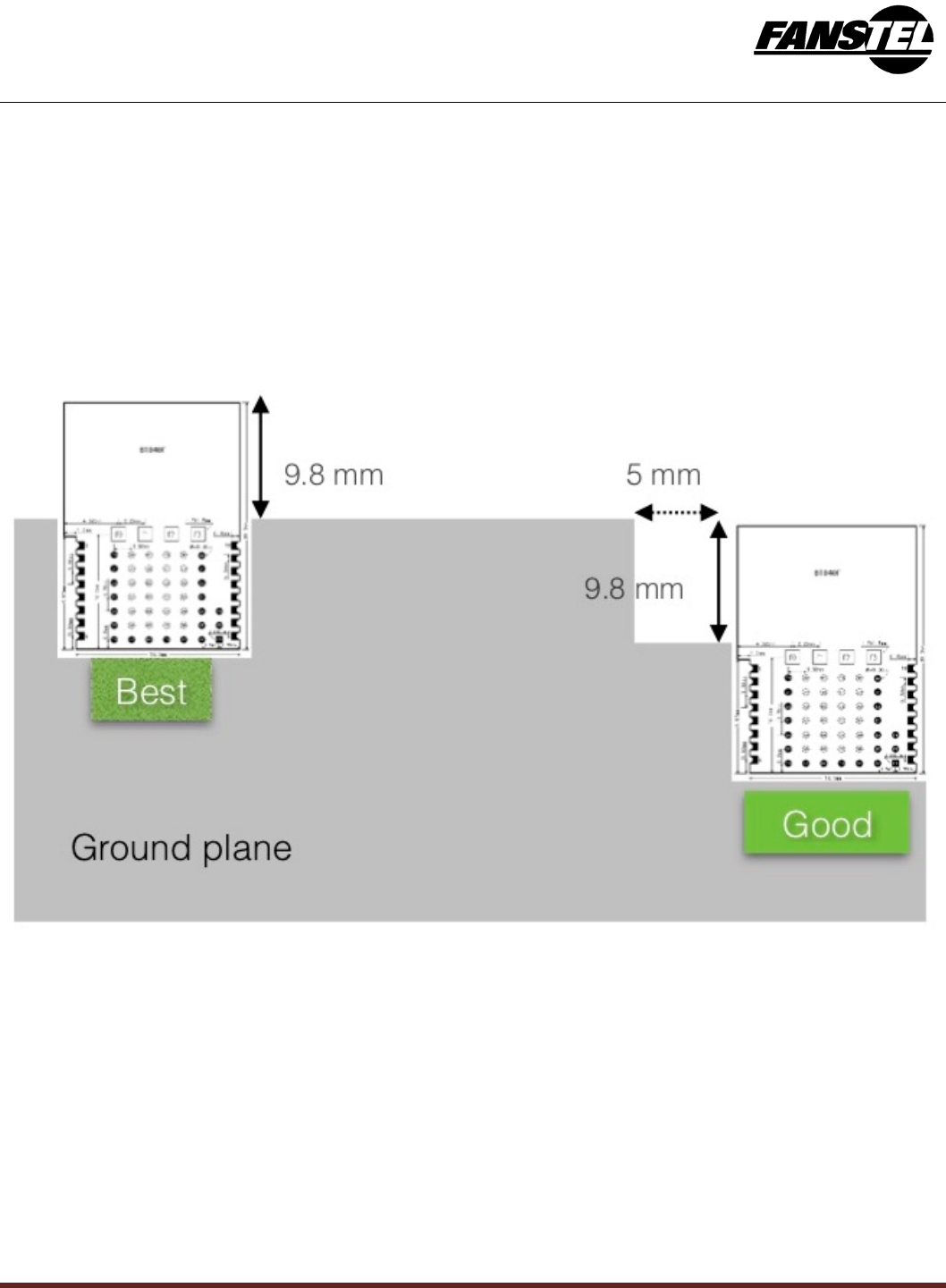
Mounting BT840F on the Host PCB
The following figure shows recommended mounting of BT840F module on the host PCB.
• For the best Bluetooth range performance, the antenna area of module shall extend 9.8 mm outside the
edge of host PCB board, or 9.8 mm outside the edge of a ground plane.
• The next choice is to place a module on a corner of host PCB, the antenna area shall extend 9.8 mm from
the edge of ground plane. Ground plane shall be at least 5 mm from the edge of the antenna area of
module.
• We don’t recommend mounting BT840F module in the middle of a host PCB.
For the best Bluetooth range performance, keep all external metal at least 30mm from the antenna area.

Bluetooth Low Energy(BLE) 5 Module BT840FVer 0.91 Nov. 2017 draft
16
Host Board Design for Low Cost or Long Range
On nRF52 series SoCs, Nordic offers various memory options and protocol supports. Fanstel offers various
antenna and power amplifier options. A host board can be designed to accommodate these nRF52 modules.
Our suggestions for host PCB design:
If your main goal is minimum PCB cost,
• use a 2-sided PCB.
• Use library component from EV BT832 Gerber files, can be downloaded from
http://www.fanstel.com/download-document/.It has 16 castellated pins plus 24 LGA pins. BT840F library
component can be used. However, signal routing can be difficult on a 2-sided PCB.
• Be sure of no metal contact in the area of 21 additional BT840F pins.
• BT840F can be mounted on a BT832 pad.
If you main goal is maximum wireless range,
• use a 4 or more layers PCB.
• Use library component from EV BT840F V4 or newer Gerber files, can be downloaded from
http://www.fanstel.com/download-document/.It has 16 castellated pins plus 45 LGA pins.
• As much ground plane under BT840F, on top side of host PCB as possible. Use EV BT840F V4
Gerber files as an example.
• If your products may need wireless range of 1350 meters at 1 Mbps, allocate physical space for a
15x28x1.9mm module. This larger module size is required to accommodate Skyworks SKY66112
power amplifier.
• Don’t use P0.06 (BT840F pin B4), P0.17 (BT840F pin C3), and P0.19 (BT840F pin D2) on the host
board. These pins are used to control SKY66112 power amplifier.

Bluetooth Low Energy(BLE) 5 Module BT840FVer 0.91 Nov. 2017 draft
17
4. BT840F Evaluation Board
Communicating with a PC
A quick and easy way to evaluate BT840F is to use a PC as the host processor. Connect the development
board EV-BT840F to a PC with an USB cable. Then,
SetS1, BT840F is set to command mode. PC will communicate with BT840F.
Set switch S1 to the other position, BT840F is set to data mode. PC will communicate with a remote device
through BT840F Bluetooth wireless connection.
Docklight is a testing, analysis and simulation tool for serial communication protocols (RS232, RS485/422 and
others). It allows you to monitor the communication between two serial devices or to test the serial
communication of a single device. Docklight significantly increases productivity in a broad range of industries,
including automation and control, communications, automotive, equipment manufacturers, and embedded /
consumer products. Docklight is easy to use and runs on almost any standard PC using Windows 10, Windows
8, Windows 7, Windows Vista or Windows XP operating system.
Docklight software can be downloaded from the following:
http://www.docklight.de/download_en.htm
B
E
V
E
v
ht
t
E
v
B
T
E
V
Pi
n
B
T
bo
Ad
1.
2.
luetoot
h
V
BT840
F
v
aluation bo
t
p://www.fa
n
v
aluation bo
T
840F sold
e
V
BT840F
V
n
s in solid
c
T
832/BT83
2
ard to acco
d
ditional fea
It has the s
a
pins of Blu
e
EV BT840
F
many UNO
h
Low
E
F
V4 Ev
a
ard schem
a
n
stel.com/d
o
ard can be
e
ring pads
w
V
4 evaluatio
n
c
olo
r
are us
e
2
F/BT832X.
mmodate
B
ture enhan
c
a
me foot pr
e
No
r
modul
e
F
is not an
U
R3 compa
t
E
nergy(
a
luation
B
a
tics and G
e
o
wnload-d
o
used as a
r
w
ith 61 pins
n
board is
d
e
d only for
B
Red color
p
B
T840F and
c
ements fo
r
int as
A
rdui
e
s.
U
NO R3 co
m
t
ible shield
s
BLE) 5
B
oard Sc
e
rbe
r
files c
o
cument/
r
eference d
e
. These 21
d
eveloped f
o
B
T840F. Bl
u
p
in names
a
BT832/BT
8
r
version V
4
no Uno R3
.
m
patible bo
a
s
.
Modul
e
18
hematic
s
an be dow
n
e
sign for us
pins in soli
d
or
BT840F
a
u
e color pin
a
re for BT8
4
8
32F/BT83
2
4
evaluation
.
Additional
a
rd. You ca
e
BT840
s
n
loaded fro
m
ing module
s
d
dark color
a
nd BT832
X
names ar
o
4
0F. Firmw
a
2
X.
board:
connectors
n use Nord
F
Ver 0.91
N
m
s
. EV BT84
are for BT
8
X
. It can be
o
und U1 BT
8
a
re pin con
f
are added
ic develop
t
N
ov. 2017 d
r
0F V4 is d
e
8
40F.
used for B
T
8
40(832) a
r
f
iguration is
for connec
t
t
ools to dev
e
r
aft
e
signed for
t
T
832 and B
T
r
e for
required fo
t
ion to extr
a
e
lop firmw
a
t
he
T832F.
r
a host
a
GPIO
a
re for

Bluetooth Low Energy(BLE) 5 Module BT840FVer 0.91 Nov. 2017 draft
19
3. Portable smartphone charger can be used to power this board. The circuitry to the left of micro USB
connector, J16 produces periodic load to prevent portable smartphone charger from shutting down.
Suggestion for Battery Power Application
Standby current consumption is important for battery-powered product. We suggest adding a 32.768 kHz
crystal and 2 capacitors on host board. The 32MHz main clock won’t be active at idle state to save power.
Two inductors required for on-board DC to DC converter are inside BT840F. You can enable DCDC converter
to have lower power consumption.
Bluetooth Low Energy(BLE) 5 Module BT840FVer 0.91 Nov. 2017 draft
20
5. Miscellaneous
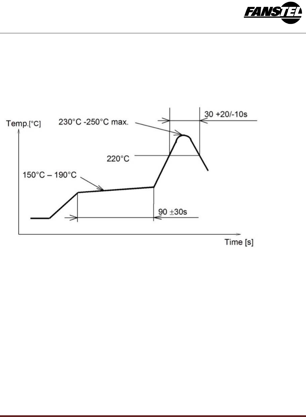
Soldering Temperature-Time Profile for Re-Flow Soldering
Maximum number of cycles for re-flow is 2. No opposite side re-flow is allowed due to module weight.
Cautions, Design Notes, and Installation Notes
Failure to follow the guidelines set forth in this document may result in degrading of the
product’sfunctions and damage to the product.
Design Notes
(1) Follow the conditions written in this specification, especially the control signals ofthis module.
(2) The supply voltage has to be free of AC ripple voltage (for example from a battery or a low noise
regulator output). For noisy supply voltages, provide a decoupling circuit (for example a ferrite in
series connection and a bypass capacitor to ground of at least 47uF directly at the module).
(3) This product should not be mechanically stressed when installed.
(4) Keep this product away from heat. Heat is the major cause of decreasing the life of these
products.
(5) Avoid assembly and use of the target equipment in conditions where the products' temperature
may exceed the maximum tolerance.

Bluetooth Low Energy(BLE) 5 Module BT840FVer 0.91 Nov. 2017 draft
21
(6) The supply voltage should not be exceedingly high or reversed. It should not carry noise and/or
spikes.
(7) this product away from other high frequency circuits.
Notes on Antenna and PCB Layout
(1) Don’t use a module with internal antenna inside a metal case.
(2) For PCB layout:
• Avoid running any signal line below module whenever possible,
• No ground plane below antenna,
• If possible, cut-off the portion of main board PCB below antenna.
Installation Notes
(1) Reflow soldering is possible twice based on the time-temperature profile in this data sheets.Set up
the temperature at the soldering portion of this product according to this reflow profile.
(2) Carefully position the products so that their heat will not burn into printed circuitboards or affect the
other components that are susceptible to heat.
(3) Carefully locate these products so that their temperatures will not increase due tothe effects of
heat generated by neighboring components.
(4) If a vinyl-covered wire comes into contact with the products, then the cover will melt and generate
toxic gas, damaging the insulation. Never allow contact between the cover and these products to
occur.
(5) This product should not be mechanically stressed or vibrated when reflowed.
(6) If you want to repair your board by hand soldering, please keep the conditions of this chapter.
(7) Do not wash this product.
(8) Refer to the recommended pattern when designing a board.
(9) Pressing on parts of the metal cover or fastening objects to the metal will cause damage to the
unit.
(10) For more details on LGA (Land Grid Array) soldering processes refer to the application note.
Usage Condition Notes
(1)Take measures to protect the unit against static electricity. If pulses or other transient loads (a
large load applied in a short time) are applied to the products, check and evaluate their operation
before assembly on the final products.
(2)Do not use dropped products.
(3)Do not touch, damage or soil the pins.
(4) Follow the recommended condition ratings about the power supply applied to thisproduct.
(5)Electrode peeling strength: Do not add pressure of more than 4.9N when soldered on PCB

Bluetooth Low Energy(BLE) 5 Module BT840FVer 0.91 Nov. 2017 draft
22
(6) Pressing on parts of the metal cover or fastening objects to the metal cover will cause damage.
(7) These products are intended for general purpose and standard use in general electronic
equipment, such as home appliances, office equipment, informationand communication equipment.
Storage Notes
(1)The module should not be stressed mechanically during storage.
(2)Do not store these products in the following conditions or the performancecharacteristics of the
product, such as RF performance will be adverselyaffected:
• Storage in salty air or in an environment with a high concentration of corrosive gas.
• Storage in direct sunlight
• Storage in an environment where the temperature may be outside the range specified.
• Storage of the products for more than one year after the date of delivery storage period.
(3) Keep this product away from water, poisonous gas and corrosive gas.
(4) This product should not be stressed or shocked when transported.
(5) Follow the specification when stacking packed crates (max. 10).
Safety Conditions
These specifications are intended to preserve the quality assurance of products and individual
components. Before use, check and evaluate the operation when mounted on your products. Abide by
these specifications, without deviation when using the products. These products may short-circuit. If
electrical shocks, smoke, fire, and/or accidents involving human life are anticipated when a short
circuit occurs, then provide the following failsafe functions, as a minimum.
(1)Ensure the safety of the whole system by installing a protection circuit and a protection device.
(2)Ensure the safety of the whole system by installing a redundant circuit or anothersystem to prevent
a dual fault causing an unsafe status.
Other Cautions
(1)This specification sheet is copyrighted. Reproduction of this data sheets is permissible only if
reproduction is without alteration and is accompanied by all associated warranties, conditions,
limitations, and notices.
(2)Do not use the products for other purposes than those listed.
(3)Be sure to provide an appropriate failsafe function on your product to prevent anadditional damage
that may be caused by the abnormal function or the failure of the product.
(4)This product has been manufactured without any ozone chemical controlled under the Montreal
Protocol.

Bluetooth Low Energy(BLE) 5 Module BT840FVer 0.91 Nov. 2017 draft
23
(5)These products are not intended for other uses, other than under the special conditions shown
below. Before using these products under such special conditions, check their performance and
reliability under the said special conditions carefully to determine whether or not they can be used
in such a manner.
• In liquid, such as water, salt water, oil, alkali, or organic solvent, or in places where liquid may
splash.
• In direct sunlight, outdoors, or in a dusty environment
• In an environment where condensation occurs.
• In an environment with a high concentration of harmful gas.
(6) If an abnormal voltage is applied due to a problem occurring in other componentsor circuits,
replace these products with new products because they may not beable to provide normal
performance even if their electronic characteristics and appearances appear satisfactory.
(7) When you have any question or uncertainty, contact Fanstel.
Packaging
Production modules are delivered in reel, 1000 modules in each reel.
FCC LABEL
The Original Equipment Manufacturer (OEM) must ensure that the OEM modular transmitter must be labeled
with its own FCC ID number. This includes a clearly visible label on the outside of the final product enclosure
that displays the contents shown below. If the FCC ID is not visible when the equipment is installed inside
another device, then the outside of the device into which the equipment is installed must also display a label
referring to the enclosed equipment
The end product with this module may subject to perform FCC part 15 unintentional emission test requirement
and be properly authorized.
This device is intended for OEM integrator only.

Bluetooth Low Energy(BLE) 5 Module BT840FVer 0.91 Nov. 2017 draft
24
6.Contact Us
United States:
Fanstel Corp.
7466 E. Monte Ctisto Ave. Scottsdale AZ 85260
Tel. 1 480-948-4928
Fax. 1-480-948-5459
Email: module@fanstel.com
Website: www.fanstel.com
Taiwan:
Fanstel Corp.
10F-10, 79 Xintai Wu Road
Xizhu, New Taipei City, Taiwan 22101
泛世公司
臺灣省新北市汐止區新臺五路 79 號10 樓之 10, 22101
Tel. 886-2-2698-9328
Fax. 886-2-2698-4813
Email: tp@fanstel.com
Website: www.fanstel.com
China:
Fanstel Technologies Corp.
11 Jiale Street
Ping-Dih, Long-Gang, Shen Zhen, GD 518117
泛世康科技(深圳)有限公司
廣東省深圳市龍崗區坪地鎮佳樂街 11 號
Tel. 86-755-8409-0928
Fax. 86-755-8409-0973
QQ. 3076221086
Email: sz@fanstel.com
Website: www.fanstel.com
Federal Communications Commission (FCC) Statement
15.21
You are cautioned that changes or modifications not expressly approved by the part responsible for compliance
could void the user’s authority to operate the equipment.
15.105(b)
This equipment has been tested and found to comply with the limits for a Class B digital device, pursuant to part
15 of the FCC rules. These limits are designed to provide reasonable protection against harmful interference in a
residential installation. This equipment generates, uses and can radiate radio frequency energy and, if not

Bluetooth Low Energy(BLE) 5 Module BT840FVer 0.91 Nov. 2017 draft
25
installed and used in accordance with the instructions, may cause harmful interference to radio communications.
However, there is no guarantee that interference will not occur in a particular installation. If this equipment does
cause harmful interference to radio or television reception, which can be determined by turning the equipment
off and on, the user is encouraged to try to correct the interference by one or more of the following measures:
-Reorient or relocate the receiving antenna.
-Increase the separation between the equipment and receiver.
-Connect the equipment into an outlet on a circuit different from that to which the receiver is connected.
-Consult the dealer or an experienced radio/TV technician for help.
This device complies with Part 15 of the FCC Rules. Operation is subject to the following two conditions:
1) this device may not cause harmful interference, and
2) this device must accept any interference received, including interference that may cause undesired operation
of the device.
FCC RF Radiation Exposure Statement
1) This Transmitter must not be co-located or operating in conjunction with any other antenna or transmitter.
2) This equipment complies with FCC RF radiation exposure limits set forth for an uncontrolled environment.
This equipment should be installed.
Note: The end product shall has the words “Contains Transmitter Module FCC ID: X8WBT832X

Bluetooth Low Energy(BLE) 5 Module BT840FVer 0.91 Nov. 2017 draft
26
Canada, Industry Canada (IC)
This Class B digital apparatus complies with Canadian ICES-003
Cet appareil numérique de classe B est conforme à la norme NMB-003.
This device complies with Industry Canada licence-exempt RSS standard(s). Operation is subject
to the following two conditions: (1) this device may not cause interference, and (2) this device
must accept any interference, including interference that may cause undesired operation of the
Le present appareil est conforme aux CNR d'Industrie Canada applicables auxappareils radio exempts de licence.L'exploitation est
autorisée aux deux conditions suivantes:
(1) l'appareil ne doit pas produire de brouillage, et
(2) l'utilisateur de l'appareil doit accepter tout brouillage adioélectrique subi, même si le brouillage est susceptible d'en compromettre
le fonctionnement.
Canada, avis d'Industry Canada (IC)
“Le présent appareil est conforme aux CNR d'Industrie Canada applicables aux appareils radio exempts de
licence. L'exploitation est autorisée aux deux conditions suivantes : (1) l'appareil ne doit pas produire de
brouillage, et (2) l'utilisateur de l'appareil doit accepter tout brouillage radioélectrique subi, même si le
brouillage est susceptible d'en compromettre le fonctionnement."
Déclaration d'exposition aux radiations:
Cet équipement est conforme aux limites d'exposition aux rayonnements ISEDétablies pour un environnement
non contrôlé. Cet équipement doit être installé et utilisé avec un minimum de 20 cm de distance entre la source
de rayonnement et votre corps.
(Modular approval) End Product Labeling:
The final end product must be labeled in a visible area with the following: “Contains IC: 4100A-BT840”.
Caution: Exposure to Radio Frequency Radiation.
To comply with RSS 102 RF exposure compliance requirements
OEM statement
The Original Equipment Manufacturer (OEM) must ensure that the OEM modular transmitter must be labeled with its own FCC ID
number. This includes a clearly visible label on the outside of the final product enclosure that displays the contents shown below. If
the FCC ID is not visible when the equipment is installed inside another device, then the outside of the device into which the
equipment is installed must also display a label referring to the enclosed equipment
The end product with this module may subject to perform FCC part 15 unintentional emission test requirement and be properly
authorized.
This device is intended for OEM integrator only