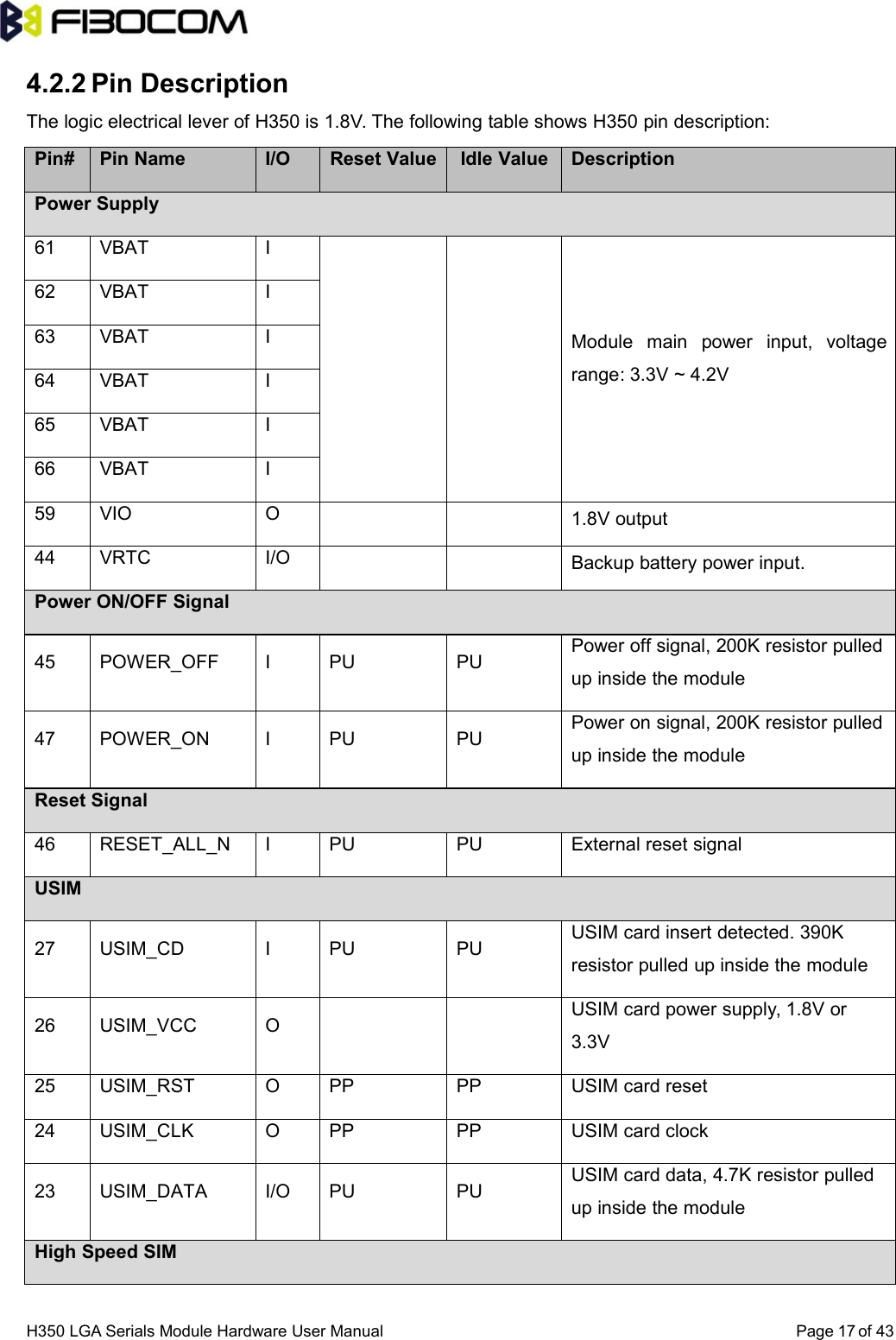
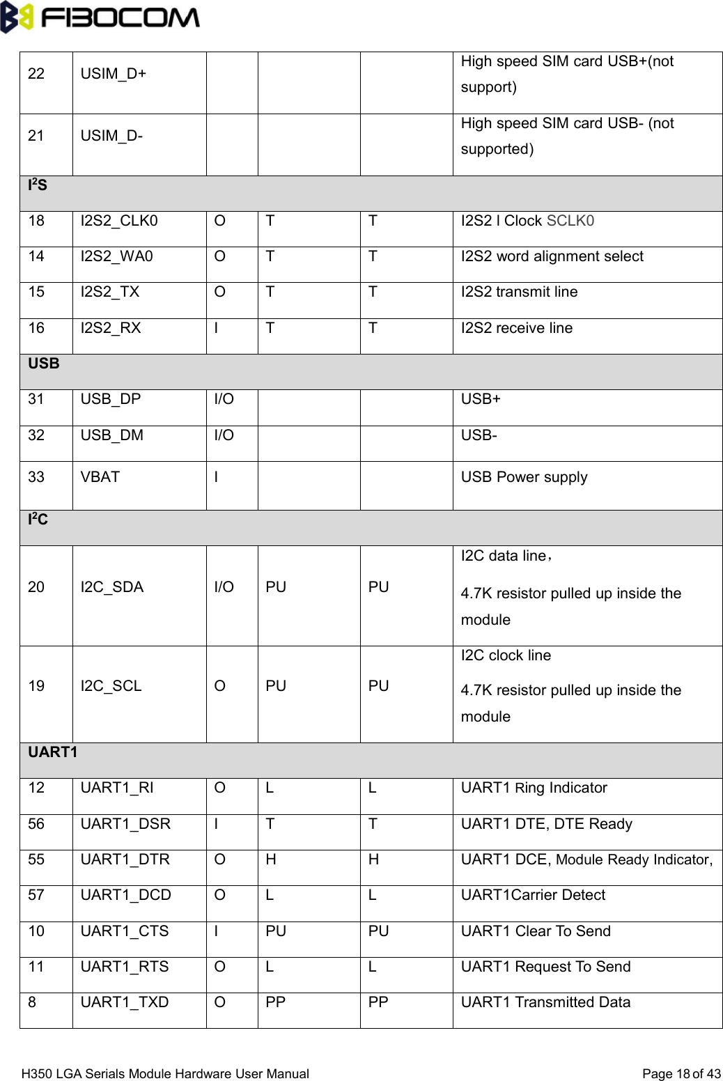
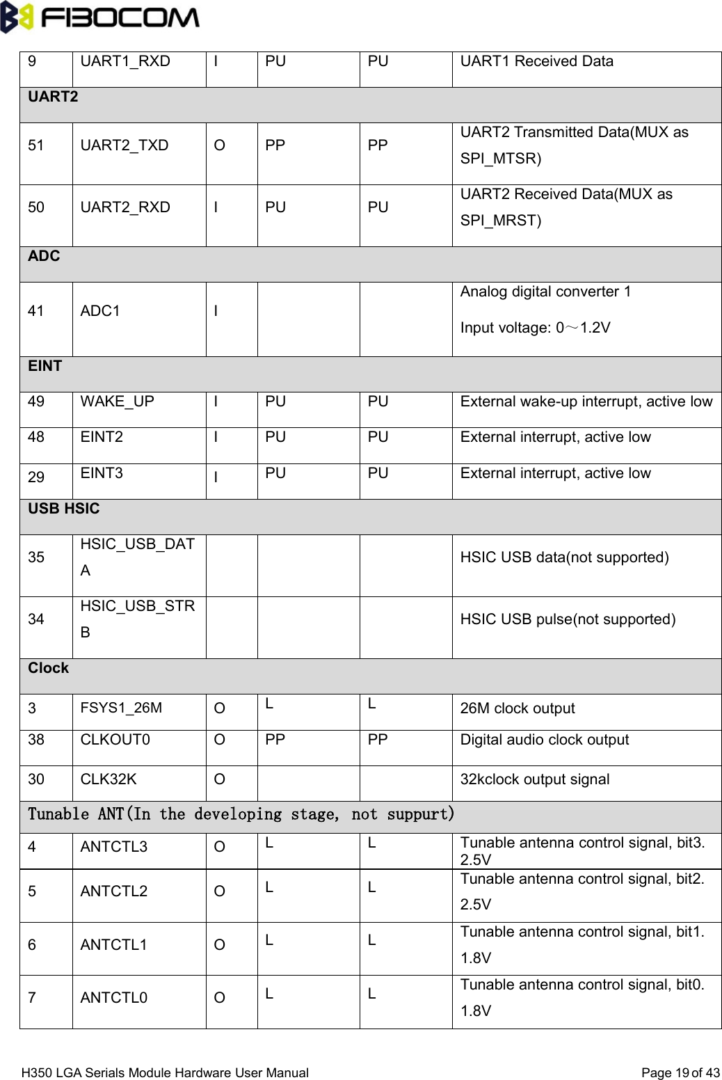
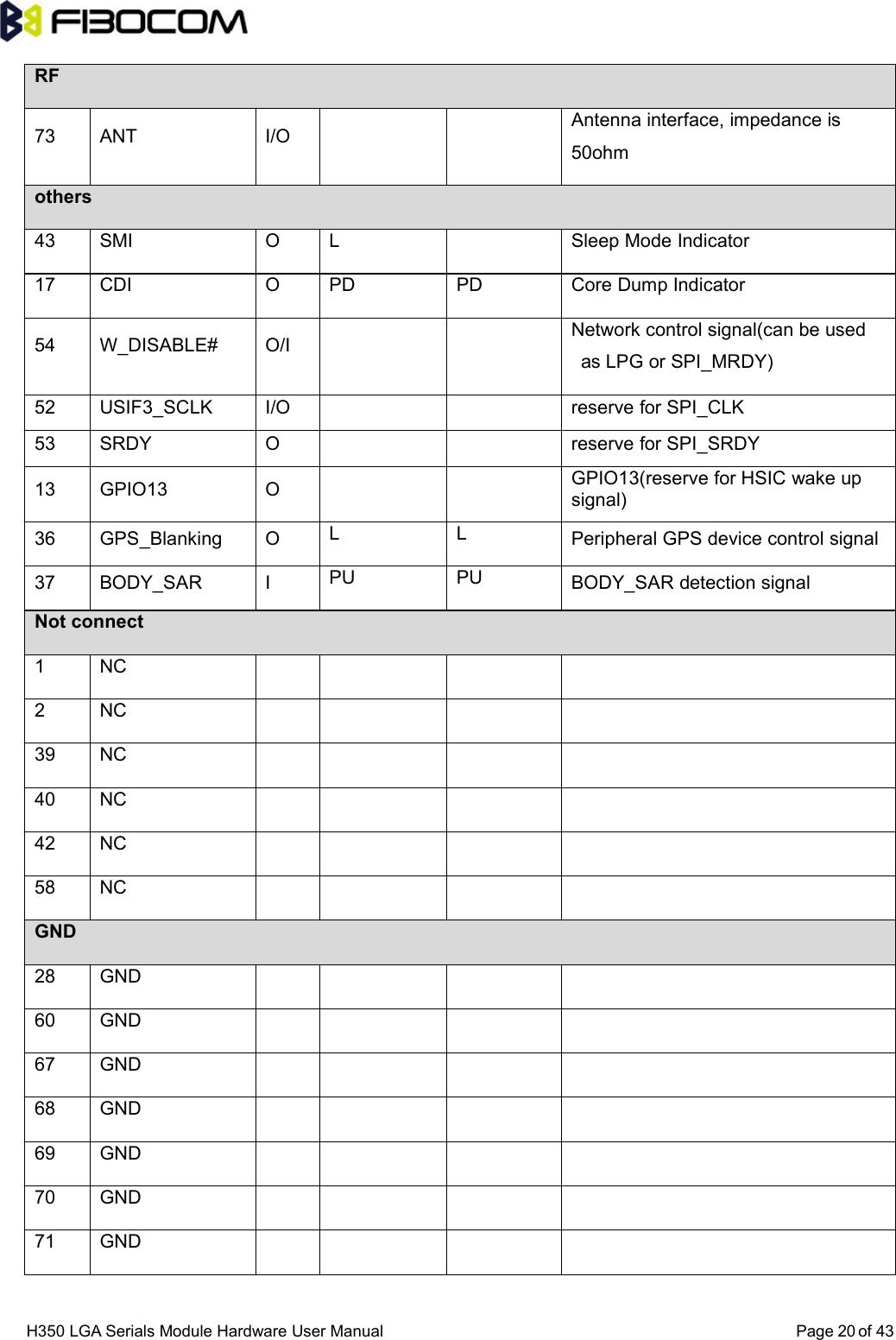
Fibocom Wireless H35F WCDMA/GSM(GPRS) Dual-band wireless module User Manual FIBOCOM H350 LGA Serials Module Hardware ver1

Fibocom Wireless Inc. WCDMA/GSM(GPRS) Dual-band wireless module FIBOCOM H350 LGA Serials Module Hardware ver1

FIBOCOM_H350 LGA Serials Module Hardware User Manual-ver1

H350 LGA Serials ModuleHardware User ManualVersion: V1.0.3Date: 2014-02-22
H350 LGA Serials Module Hardware User Manual Page of 432Confidential MaterialThis document contains information highly confidential to Fibocom Wireless Inc. (Fibocom). Fibocomoffers this information as a service to its customers, to support application and engineering efforts that usethe products designed by Fibocom. The information provided is based upon requirements specificallyprovided to Fibocom by the customers. All specifications supplied herein are subject to change.Disclosure of this information to other parties is prohibited without the written consent of Fibocom.CopyrightCopy, Reproduce, Distribute and/or Edit of this document or part of it as well as utilization of its contentsand communication thereof to others without express authorization are prohibited. Offenders will be heldliable for payment of damages. All rights created by patent grant or registration of a utility model or designpatent are reserved. Copyright ©2013 Fibocom Wireless Inc. All rights reserved.Trademarks NoticeThe FIBOCOM Logo is registered by Fibocom Wireless Inc. All other product or service names or logosare the property of their respective owners. Copyright ©2013 Fibocom Wireless Inc. All rights reserved.
H350 LGA Serials Module Hardware User Manual Page of 433Federal Communication Commission Interference StatementThis device complies with Part 15 of the FCC Rules. Operation is subject to the following two conditions:(1)This device may not cause harmful interference.(2) This device must accept any interference received,including interference that may cause undesiredoperation.This equipment has been tested and found to comply with the limits for a Class B digital device,pursuantto Part 15 of the FCC Rules. These limits are designed to provide reasonable protection against harmfulinterference in a residential installation. This equipment generates, uses and can radiate radio frequencyenergy and, if not installed and used in accordance with the instructions,may cause harmful interferenceto radio communications. However, there is no guarantee that interference will not occur in a particularinstallation. If this equipment does cause harmful interference to radio or television reception, which canbe determined by turning the equipment off and on, the user is encouraged to try to correct theinterference by one of the following measures:- Reorient or relocate the receiving antenna.- Increase the separation between the equipment and receiver.- Connect the equipment into an outlet on a circuit different from that to which the receiver is connected.- Consult the dealer or an experienced radio/TV technician for help.FCC Caution: Any changes or modifications not expressly approved by the party responsible forcompliance could void the user's authority to operate this equipment.This transmitter must not be co-located or operating in conjunction with any other antenna or transmitter.RF Exposure Compliance:This equipment complies with FCC radiation exposure limits set forth for an uncontrolled environment.Theantenna(s) used for this transmitter must be installed to provide a separation distance of at least 20conform all persons and must not be co-located or operating in conjunction with any other antenna ortransmitter.This device is intended only for OEM integrators under the following conditions:1) The antenna must be installed such that 20 cm is maintained between the antenna and users.2) The transmitter module may not be co-located with any other transmitter or antenna.As long as 2 conditions above are met, further transmitter test will not be required. However, the OEMintegrator is still responsible for testing their end-product for any additional compliance requirementsrequired with this module installedIMPORTANT NOTE:In the event that these conditions can not be met (for example certain laptop configurations or co-locationwith another transmitter), then the FCC authorization is no longer considered valid and the FCC ID cannot be used on the final product. In these circumstances, the OEM integrator will be responsible forre-evaluating the end product(including the transmitter) and obtaining a separate FCC authorization.End Product Labeling:This transmitter module is authorized only for use in device where the antenna may be installed such that20 cm may be maintained between the antenna and users. The final end product must be labeled in avisible area with the following contains:FCC ID:ZMOH35F .The grantee's FCC ID can be used only when all FCC compliance requirements
H350 LGA Serials Module Hardware User Manual Page of 434are met.Manual Information To the End User:The OEM integrator has to be aware not to provide information to the end user regarding how to install orremove this RF module in the user’s manual of the end product which integrates this module.The end user manual shall include all required regulatory information/warning as show in this manual.
H350 LGA Serials Module Hardware User Manual Page of 435Revision HistoryVersion Date RemarksV1.0.0 2014-01-09 Initial VersionV1.0.1 2014-01-15 Modified PIN description tableV1.0.2 2014-01-16 Modified tunable antenna levelV1.0.3 2014-02-22 Add H350-B50-10 descriptionApplicability TableNo. Type Note1 H350-A50-102 H350-A30-103 H350-B50-104 H350-B30-10Here are the module comparisons:Model No. GSM/GPRS/EDGEBand(MHz)WCDMABand(MHz)HSDPA(Mbps)HSUPA(Mbps)H350-A50-10 900/1800 900/2100 21 5.76H350-A30-10 900/1800 900/2100 7.2 5.76H350-B50-10 850/1900 850/1900 21 5.76H350-B30-10 850/1900 850/1900 7.2 5.76
H350 LGA Serials Module Hardware User Manual Page of 436Contents1 Preface....................................................................................................................................................................... 81.1 Scope.............................................................................................................................................................. 81.2 Standards....................................................................................................................................................... 82 Introduction.............................................................................................................................................................. 102.1 Description................................................................................................................................................... 102.2 Specifications...............................................................................................................................................102.3 Appearance.................................................................................................................................................. 123 Mechanical...............................................................................................................................................................153.1 Dimensions...................................................................................................................................................153.2 PCB Layout Design.................................................................................................................................... 164 Hardware Overview................................................................................................................................................174.1 Block Diagram............................................................................................................................................. 174.2 Pin Definition................................................................................................................................................ 184.2.1 Pin Map............................................................................................................................................. 184.2.2 Pin Description................................................................................................................................. 195 Hardware Interface.................................................................................................................................................245.1 Power Interface........................................................................................................................................... 245.1.1 VBAT.................................................................................................................................................. 245.1.2 Power Consumption........................................................................................................................255.1.3 VIO..................................................................................................................................................... 275.1.4 VRTC................................................................................................................................................. 275.2 ON/OFF and Reset.....................................................................................................................................285.2.1 Pin Definition.................................................................................................................................... 285.2.2 Power ON Signal............................................................................................................................. 285.2.3 Power off Signal............................................................................................................................... 295.2.4 Reset Signal..................................................................................................................................... 305.3 Indicator Signal............................................................................................................................................315.3.1 Pin Description................................................................................................................................. 315.3.2 Indicator Description....................................................................................................................... 315.4 USB Interface...............................................................................................................................................325.4.1 USB Interface Description..............................................................................................................325.4.2 USB Interface Application.............................................................................................................. 33
H350 LGA Serials Module Hardware User Manual Page of 4375.5 UART Interface............................................................................................................................................ 335.5.1 UART Interface Description........................................................................................................... 335.5.2 UART Design....................................................................................................................................355.5.3 Ring Indicator................................................................................................................................... 355.6 USIM..............................................................................................................................................................365.6.1 USIM Interface................................................................................................................................. 365.6.2 USIM.................................................................................................................................................. 365.6.3 USIM Design Notice........................................................................................................................385.6.4 USIM Hot Plug..................................................................................................................................395.7 Digital Audio................................................................................................................................................. 405.7.1 I2S...................................................................................................................................................... 405.7.2 I2C...................................................................................................................................................... 405.7.3 PCM Mode Interface....................................................................................................................... 415.8 ADC Interface...............................................................................................................................................415.9 GPS_BLANKING........................................................................................................................................ 415.10 BODY_SAR............................................................................................................................................... 425.11 Clock............................................................................................................................................................425.12 Others......................................................................................................................................................... 426 Electrical and Environmental Features............................................................................................................... 436.1 Electrical Features...................................................................................................................................... 436.2 Environmental Features.............................................................................................................................437 RF Interface............................................................................................................................................................. 447.1 Operation Frequency Band....................................................................................................................... 447.1.1 Main Antenna....................................................................................................................................447.2 RF PCB Design........................................................................................................................................... 447.2.1 Layout Guideline.............................................................................................................................. 447.2.2 Impedance........................................................................................................................................ 447.3 Antenna Design........................................................................................................................................... 457.3.1 Main Antenna Design Requirements........................................................................................... 45
H350 LGA Serials Module Hardware User Manual Page of 4381 Preface1.1 ScopeThis manual provides the electrical, mechanical and environmental requirements for properly integratingthe H350 serials wireless communications module. This manual gives a complete set of hardwarefeatures and functions that may be provided by H350, ensures the users can quickly and convenientlydevelop wireless communications using H350 Module.1.2 Standards3GPP TS 27.007 -v6.9.0: AT command set for User Equipment (UE)3GPP TS 27.005 -v6.0.1: Use of Data Terminal Equipment -Data Circuit terminating Equipment(DTE-DCE) interface for Short Message Service (SMS) and Cell Broadcast Service (CBS)3GPP TS 23.040 -v6.9.0: Technical realization of Short Message Service (SMS)3GPP TS 24.011 -v6.1.0: Point- to - Point (PP) Short Message Service (SMS) support on mobileradio interface3GPP TS 27.010 -v6.0.0: Terminal Equipment to User Equipment (TE-UE) multiplexer protocol3GPP TS 27.060 -v6.0.0: Packet domain; Mobile Station (MS) supporting Packet Switched services3GPP TS 25.304-v6.10.0: User Equipment (UE) procedures in idle mode and procedures for cellreselection in connected mode3GPP TS 25.308 -v6.4.0: High Speed Downlink Packet Access (HSDPA); Overall description;Stage 23GPP TS 25.309 -v6.6.0: FDD enhanced uplink; Overall description; Stage 23GPP TS 23.038 -v6.1.0: Alphabets and language - specific information3GPP TS 21.111 -v6.3.0: USIM and IC card requirements3GPP TS 31.111 -v6.11.0 "USIM Application Toolkit (USAT)"3GPP TS 45.002 -v6.12.0: Multiplexing and multiple access on the radio path3GPP TS 51.014 -v4.5.0: Specification of the SIM Application Toolkit for the Subscriber IdentityModule - Mobile Equipment (SIM-ME) interface3GPP TS 51.010 -1 -v6.7.0: Mobile Station (MS) conformance specification; Part 1: Conformancespecification3GPP TS 22.004 -v6.0.0: General on supplementary services3GPP TS 23.090 -v6.1.0: Unstructured Supplementary Service Data (USSD); Stage 2
H350 LGA Serials Module Hardware User Manual Page of 4393GPP TS 24.008 v6.19, Mobile radio interface Layer 3 specification;
H350 LGA Serials Module Hardware User Manual Page of 43102 Introduction2.1 DescriptionH350 serials are highly integrated 3G wireless communication modules, support GSM / GPRS / EDGEand UMTS / HSDPA / HSUPA / HSPA+.2.2 SpecificationsSpecificationsBandsH350-Axx-10 H350-Bxx-10UMTS (WCDMA/FDD):900/2100MHzUMTS (WCDMA/FDD): 850/1900MHzGSM/GPRS/EDGE: 900/1800MHz GSM/GPRS/EDGE: 850/1900MHzDataUMTS/HSDPA/HSUPA 3GPP release 7HSUPA 5.76Mbps (Cat 6)HSDPA 21Mbps (Cat 14) or 7.2Mbps (Cat 8)GSM 3GPP release 7EDGE (E-GPRS) multi-slot class 33(296kbps DL, 236.8kbps UL)GPRS multi-slot class 33(107kbps DL, 85.6kbps UL)PhysicalDimension: 29.8mm x 17.8mm x 2.00mmInterface: LGAWeight: 2.5 gramsEnvironmentOperating Temperature: -30℃~ +85℃Storage Temperature: -40℃~ +85℃PerformanceOperatingVoltageVoltage: 3.3V ~ 4.5V Normal: 3.8VOperatingCurrent (TypicalValue)2mA (Sleep Mode)3G Idle: 13mA3G Talk: 500mA2G Talk: 260mA (GSM PCL5)Tx Power(Typical Value)Class 4 (2W):850/900 MHz, GSMClass 1 (1W):1800/1900 MHz, GSMClass E2 (0.5W):850/900 MHz, EDGE
H350 LGA Serials Module Hardware User Manual Page of 4311Class E2 (0.4W):1800/1900 MHz, EDGEClass 3 (0.2W):900/850/1900/2100 MHz, WCDMARx Sensitivity(Typical Value)UMTS/HSPA: -109dBmGSM: -108dBmInterfacesRF Interface AntennaConnectivity1 x USB 2.02 x UARTMUX Over UART1Multiple Profiles over USBSPI SupportI2C SupportI2S SupportPCM, HSIC, GPIO, A/D, RTCData FeaturesProtocol Stack Embedded TCP/IP and UDP/IP protocol stackEDGEMulti-slot class 33(5 Down; 4 Up; 6 Total)Coding Scheme MCS1~9GPRSMulti-slot class 33(5 Down; 4 Up; 6 Total)Coding Scheme CS1~4CSD UMTS(14.4kbps), GSM(9.6kbps)USSD SupportSMSMO / MT Text and PDU modesCell broadcastVoice FeaturesDigital AudioVoice coders: EFR/HR/FR/AMRAudio Control Gain ControlCharacter SetIRAGSMUCS2HEXAT Commands FIBOCOM proprietary AT commands
H350 LGA Serials Module Hardware User Manual Page of 4312GSM 07.05GSM 07.07AccessoriesFirmware Loader Tool over USB/UARTUser ManualDeveloper Kit2.3 AppearanceThe following picture shows the H350 Wireless Communication Module.Top view:Figure 2- 1 Top ViewBottom view:Figure 2- 2 Bottom View
H350 LGA Serials Module Hardware User Manual Page of 43133 Mechanical3.1 DimensionsFigure 3- 1 Mechanical Specifications
H350 LGA Serials Module Hardware User Manual Page of 43143.2 PCB Layout DesignFigure 3- 2 Recommended PCB Layout
H350 LGA Serials Module Hardware User Manual Page of 43154 Hardware Overview4.1 Block DiagramFigure 4- 1 Block Diagram
H350 LGA Serials Module Hardware User Manual Page of 43164.2 Pin Definition4.2.1 Pin MapTOP (View)Figure 4- 2 Pin Definition
H350 LGA Serials Module Hardware User Manual Page of 43174.2.2 Pin DescriptionThe logic electrical lever of H350 is 1.8V. The following table shows H350 pin description:Pin# Pin Name I/O Reset Value Idle Value DescriptionPower Supply61 VBAT IModule main power input, voltagerange: 3.3V ~ 4.2V62 VBAT I63 VBAT I64 VBAT I65 VBAT I66 VBAT I59 VIO O 1.8V output44 VRTC I/O Backup battery power input.Power ON/OFF Signal45 POWER_OFF I PU PU Power off signal, 200K resistor pulledup inside the module47 POWER_ON I PU PU Power on signal, 200K resistor pulledup inside the moduleReset Signal46 RESET_ALL_N I PU PU External reset signalUSIM27 USIM_CD I PU PU USIM card insert detected. 390Kresistor pulled up inside the module26 USIM_VCC O USIM card power supply, 1.8V or3.3V25 USIM_RST O PP PP USIM card reset24 USIM_CLK O PP PP USIM card clock23 USIM_DATA I/O PU PU USIM card data, 4.7K resistor pulledup inside the moduleHigh Speed SIM
H350 LGA Serials Module Hardware User Manual Page of 431822 USIM_D+ High speed SIM card USB+(notsupport)21 USIM_D- High speed SIM card USB- (notsupported)I2S18 I2S2_CLK0 O T T I2S2 l Clock SCLK014 I2S2_WA0 O T T I2S2 word alignment select15 I2S2_TX O T T I2S2 transmit line16 I2S2_RX I T T I2S2 receive lineUSB31 USB_DP I/O USB+32 USB_DM I/O USB-33 VBAT I USB Power supplyI2C20 I2C_SDA I/O PU PUI2C data line,4.7K resistor pulled up inside themodule19 I2C_SCL O PU PUI2C clock line4.7K resistor pulled up inside themoduleUART112 UART1_RI O L L UART1 Ring Indicator56 UART1_DSR I T T UART1 DTE, DTE Ready55 UART1_DTR O H H UART1 DCE, Module Ready Indicator,57 UART1_DCD O L L UART1Carrier Detect10 UART1_CTS I PU PU UART1 Clear To Send11 UART1_RTS O L L UART1 Request To Send8 UART1_TXD O PP PP UART1 Transmitted Data
H350 LGA Serials Module Hardware User Manual Page of 43199 UART1_RXD I PU PU UART1 Received DataUART251 UART2_TXD O PP PPUART2 Transmitted Data(MUX asSPI_MTSR)50 UART2_RXD I PU PU UART2 Received Data(MUX asSPI_MRST)ADC41 ADC1 IAnalog digital converter 1Input voltage: 0~1.2VEINT49 WAKE_UP I PU PU External wake-up interrupt, active low48 EINT2 I PU PU External interrupt, active low29 EINT3 IPU PU External interrupt, active lowUSB HSIC35 HSIC_USB_DATAHSIC USB data(not supported)34 HSIC_USB_STRBHSIC USB pulse(not supported)Clock3FSYS1_26M OL L 26M clock output38 CLKOUT0 O PP PP Digital audio clock output30 CLK32K O 32kclock output signalTunable ANT(In the developing stage, not suppurt)4 ANTCTL3 O L L Tunable antenna control signal, bit3.2.5V5 ANTCTL2 O L L Tunable antenna control signal, bit2.2.5V6 ANTCTL1 O L L Tunable antenna control signal, bit1.1.8V7 ANTCTL0 O L L Tunable antenna control signal, bit0.1.8V
H350 LGA Serials Module Hardware User Manual Page of 4320RF73 ANT I/O Antenna interface, impedance is50ohmothers43 SMI O L Sleep Mode Indicator17 CDI O PD PD Core Dump Indicator54 W_DISABLE# O/I Network control signal(can be usedas LPG or SPI_MRDY)52 USIF3_SCLK I/O reserve for SPI_CLK53 SRDY O reserve for SPI_SRDY13 GPIO13 O GPIO13(reserve for HSIC wake upsignal)36 GPS_Blanking O L L Peripheral GPS device control signal37 BODY_SAR I PU PU BODY_SAR detection signalNot connect1 NC2 NC39 NC40 NC42 NC58 NCGND28 GND60 GND67 GND68 GND69 GND70 GND71 GND
H350 LGA Serials Module Hardware User Manual Page of 432172 GND74 GND75 GND76 GND77 GND78 GND79 GND80 GND81 GND82 GND83 GND84 GND85 GND86 GND87 GND88 GND89 GND90 GND91 GND92 GND93 GND94 GND95 GND96 GND97 GND98 GND99 GND
H350 LGA Serials Module Hardware User Manual Page of 4322100 GND101 GND102 GND103 GND104 GND105 GND106 GND107 GND108 GND109 GND110 GNDH:High Voltage LevelL:Low Voltage LevelPD:Pull-DownPU:Pull-UpT:TristateOD:Open DrainPP:Push-Pull5 Hardware Interface5.1 Power Interface5.1.1 VBATH350 module requires a 3.3 V~ 4.2V DC power supply to provide 2A as GSM transmitter maximumcurrent.
H350 LGA Serials Module Hardware User Manual Page of 4323Input power supply requirements:Parameter Minimum Value Recommended Value Maximum Value UnitVBAT 3.3 3.8 4.5 VNote:1. Supply voltage fluctuations need to be lower than 300mV.2. Supply voltage drop minimum value needs to be higher than 3.3V.Filter capacitor description:Recommendedcapacitor Application Description1000uF GSM Transmit currentsergeMinimizes power supply losses duringtransmit bursts. Use high capacitance valueas possible as you can.10nF, 100nF Digital signal noiseFiltering interference from clock and datasources8.2pF, 10pF 1800/1900/2100 MHzbandsFilters transmission EMI.33pF, 39pF 850/900 MHz bands Filters transmission EMI.5.1.2 Power ConsumptionParameter Description Condition Typical Value UnitIOFF RTC mode 68 uAIIDLEIdle mode(GSM) MFRMS 5 12.1 I IDLEWCDMA DRX 8 12.5ISLEEPLow power mode(GSM)DRX2 1.9ISLEEP5 1.59 1.5Low power mode(WCDMA)DRX6 1.88 1.89 1.7IGSM-RMSGSM voice -1 TX slot1 RX slot PeakcurrentDuring TX slotGSM850 PCL5 239.00IGSM-RMS10 81.8015 50.1019 46.30EGSM900 5 246.7
H350 LGA Serials Module Hardware User Manual Page of 4324PCL 10 91.915 61.219 57.2DCS1800 PCL0 172.25 82.110 60.315 57.9PCS1900 PCL0 168.805 70.7010 48.8015 46.10IGSM-MAXGSM850 PCL5 1799.90IGSM-MAX10 421.10EGSM900PCL=10GSM voice -1Rx slotTX slot15 143.6019 116.40DCS1800PCL=0EGSM900PCL5 1738.810 415.9DCS1800PCL10GSM voice -1Rx slotTX slot15 135.319 124.2DCS1800 PCL0 1012.95 348.7EGSM900PCL=15GSM voice -1Rx slotTX slot10 141.515 110.3DCS1800PCL=2 PCS1900 PCL0 1162.105 343.80DCS1800PCL=10GSM voice -1Rx slotTX slot10 139.5015 116.20IGPRSGSM850 PCL=5GSM850PCL=10EGSM900PCL=5GSM voice -1RX slotTX slot1 223.90IGPRS4 364.201 85.004 214.70
H350 LGA Serials Module Hardware User Manual Page of 4325EGSM900PCL=10Band81 247.94 373.71 894 220.35.1.3 VIOVIO is power supply for the digital portion of the circuit inside of the module; it can be used for indicatingsignal of the module. VIO can be used as a reference level of the module digital signal.Parameter Minimum Value Recommended Value Maximum Value UnitVIO @working 1.773 1.8 1.827 V5.1.4 VRTCVRTC supplies power for RTC clock inside the module, can be connected to external RTC battery.Parameter Minimum Value Recommended Value Maximum Value UnitVRTC output voltage 1.71 1.8 1.89 VVRTC input voltage(RTC is working) 0.5 1.8 1.89 VVRTC input current(RTC is working) 1.0 uAVRTC Reference design:Figure 5- 1 VRTC Reference Design
H350 LGA Serials Module Hardware User Manual Page of 4326Note:R8 is the current-limiting resistance in order to ensure VRTC working normally. R8 ≥1kohmVRTC Current consumption < 2uA;C9 value can affect RTC hold timeYou can refer to the following formula to calculate the RTC hold time: T= (1.8-0.5)*C/1=1.3C,unit: sFor example: If C9 use 100uF capacitance, the RTC can hold about 130s.Just don’t connect pin VRTC if no need RTC function.5.2 ON/OFF and Reset5.2.1 Pin DefinitionH350 wireless communication module has three control signals: power on, off and reset the module.Pin Definition:Pin# Pin Name Electrical Level Description45 POWER_OFF CMOS 1.8V Power off signal47 POWER_ON CMOS 1.8V Power on signal46 RESET_ALL_N CMOS 1.8V External reset signal input5.2.2 Power ON SignalAfter the module is powered on, users can lower down the POWER_ON signal, then module boots up.The following table shows the burst timing:Parameter Condition Minimum Value Typical Value Maximum Value UnitPulse Width 100 300 3000 msTiming control:Figure 5- 2 Timing Control
H350 LGA Serials Module Hardware User Manual Page of 4327Reference design:Figure 5- 3 POWER_ON Reference Design5.2.3 Power off SignalAfter lower down POWER_OFF signal, the power manage unit (PMU) of module is reset, modulechanges to shutdown status.Parameter Condition Minimum Value Typical Value Maximum Value UnitPulse Width 100 300 3000 msTiming control:Figure 5- 4 Timing Control
H350 LGA Serials Module Hardware User Manual Page of 4328Reference design:Figure 5- 5 POWER_OFF Reference Design5.2.4 Reset SignalH350 wireless communication module supports external reset; it can restore the module to defaultsettings through Reset signal.When Reset signal is Active Low by 100ms, the module will reset and restart. When users reset themodule, PMU inside the module is still on.Note: Reset signal is sensitive, when PCB layout, please keep it away from radio frequency interference,add debouncing capacitor near the module end is recommended. Don’t trace the Reset signal in PCBedge or surface, it may reset ESD.Pulse Timing requirements:Parameters Condition Minimum Value Typical Value Maximum Value UnitPulse Width 100 300 3000 msRecommended design:Figure 5- 6 Reset Recommended Design
H350 LGA Serials Module Hardware User Manual Page of 43295.3 Indicator Signal5.3.1 Pin DescriptionPin# Pin Name Description54 W_DISABLE1#/LPG Open/close network/state indication43 SMI Sleep Mode Indicator17 CDI Core Dump Indicator49 WAKE_UP Wake up module5.3.2 Indicator Description5.3.2.1 LPG SignalLPG signal description:Status Modeidle(unregistered) high level: about 2.5s, low level: about 100msidle(registered) 75ms high level, 3S low levelCall low levelData communicating 75ms high level, 75ms low levelSleep high levelNote: High level voltage is 1.8V.5.3.2.2 SMIModule Mode ModeSleep Mode 2.5S High level; 100ms Low level alternate changeOther Mode low level5.3.2.3 CDI IndicatorUsed for Core dump indicator.Module Mode ModeNormal mode low levelCore Dump High level
H350 LGA Serials Module Hardware User Manual Page of 43305.3.2.4 WAKE_UPModule Mode WAKE_UP Signal DescriptionSleepLow level Wake up module, switch from Sleep to IdleHigh level Stay in Sleep modeIdle/CallLow level Keep mode, no affectHigh level Module cannot set to Sleep mode5.4 USB Interface5.4.1 USB Interface DescriptionPin# Pin Name I/O Description31 USB_DP I/O USB+32 USB_DM I/O USB-33 VBAT I USB power supplyH350 wireless communication module supports USB 2.0. Install the corresponding USB driver before useon PC. After H350 wireless communication module plugged into the PC, the USB can map seven ports:One 3G Modem/AT port for data operationThree ports for sending AT CommandOne port for traceTwo ports are reserved
H350 LGA Serials Module Hardware User Manual Page of 43315.4.2 USB Interface ApplicationReference Design:Figure 5- 7 USB Interface Reference DesignT101 and T102 should be low capacitor TVS, it is below 1pF. No special requirement for T103.VUSB is USB power supply, Recommend power supply range is 3.3V ~ 4.5V. Please don’t float pinVUSB, or USB can’t be detected.USB_DP and USB_DM are high speed differential lines, the highest transmit speed is 480 Mbps.PCB Layout note:USB_DP and USB_DM lines need equal length, parallel, as short as possible.The input and output need GND isolation.The layout design of this circuit on the AP board should comply with the USB 2.0 high speed protocol,With differential lining and impedance control to 90 ohm.5.5 UART Interface5.5.1 UART Interface DescriptionH350 wireless communication module provides two UART, one is 8 wire serial bus interface, and theother is a 2 wire serial bus interface.8 wire serial bus interface (UART1) supports flow control; users can download software or send/receiveAT through UART1. 2 wire serial bus interface (UART2) supports a few AT Commands.Note:UART2 only supports some common query functions.UART2 doesn’t support hardware flow control, no CTS, RTS, DTR, DSR, DCD, RI pin.
H350 LGA Serials Module Hardware User Manual Page of 4332UART2 support MUX as SPI interface.UART1 and UART2 signal description:UART1Pin# Pin Name I/O Description12 UART1_RI O UART1 Ring Indicator56 UART1_DSR I UART1 DTE Ready55 UART1_DTR O UART1 DCE Ready57 UART1_DCD O UART1 Carrier Detect10 UART1_CTS I UART1 Clear to send11 UART1_RTS O UART1 Request to send8 UART1_TXD O UART1 Transmitted Data9 UART1_RXD I UART1 Received DataUART2Pin# Pin Name I/O Description50 UART2_RXD I UART2 Transmitted Data51 UART2_TXD O UART2 Received Data5.5.2 UART DesignThe following table show the signal direction when H350 wireless communication module (DCE) UART1connects to PC (DTE):Application MCU(DTE) Signal Direction H350 Module (DCE)RXD UART1_TXDTXD UART1_RXDRTS UART1_CTSCTS UART1_RTSDSR UART1_DTRDTR UART1_DSR
H350 LGA Serials Module Hardware User Manual Page of 4333RI UART1_RIDCD UART1_DCDThe following table shows the signal direction when H350 wireless communication module (DCE) UART2connects to PC (DTE):Application MCU(DTE) Signal Direction H350 Module (DCE)RXD UART2_TXDTXD UART2_RXDNote: Module UART high level is 1.8V, please use external level shifter if connect to 2.8V or 3.3V IOinterface.When you design:Level shift from 1.8V to 3.3V, SN74LVC2G07 is recommended.When UART1 communicating with PC, first translates from 1.8V to 3.3V, and then uses SP3238 totranslate.When UART2 communicating with PC, first translates from 1.8V to 3.3V, and then uses SPIEX3232EEAto translate level. Notice the signal direction when translate level.5.5.3 Ring IndicatorUART1_R1 is used for indicating incoming call and SMS, sending pulse to host application program.Operation Mode StatusDefault mode Low levelRinging 1s high level, 1s low level, cyclingIncoming message 150ms pulse5.6 USIMH350 wireless communication module supports USIM and high speed SIM card, does not support 8 linesmart USIM yet.5.6.1 USIM InterfacePin# Pin Name I/O Description26 USIM_VCC O USIM power supply output25 USIM_RST O USIM Reset signal
H350 LGA Serials Module Hardware User Manual Page of 433424 USIM_CLK O USIM clock signal23 USIM_IO I/O USIM data signal28 GND GND USIM ground27 USIM_CD IUSIM insert detect signalLow level indicates SIM card is not insertedHigh level indicates SIM card is inserted5.6.2 USIM5.6.2.1 Normally Closed SIM Circuit DesignReference Design:Figure 5- 8 Normally Closed SIM Interface Reference DesignNormally closed SIM:1)Pull out SIM card, pin 7 and pin 8 are shorted.2)Plug SIM card, pin 7 and pin 8 are disconnected.
H350 LGA Serials Module Hardware User Manual Page of 43355.6.2.2 Normally Open SIM Circuit DesignReference Design:Figure 5- 9 Normally Open SIM Interface Reference DesignNormally Open SIM:1)Pull out SIM card, pin 7 and pin 8 are disconnected.2)Inset SIM card, pin 7 and pin 8 are shorted.Note:For better EMC performance, SIM card holder should be close to moduleFiltering capacitor should be close to SIM card pinThe interface need add ESD protection, ESD should be close to SIM card pinUSIM_IO is already pulled up inside the moduleUSIM_CD support SIM hot plug, high level activated default (detect level can be changed by ATcommand). If high level is detected, it means SIM card is inserted.5.6.3 USIM Design NoticeThe SIM interface and signals design is extremely important.There are several design guidelines that must be followed:
H350 LGA Serials Module Hardware User Manual Page of 4336The layout signals of the SIM card should be away from any possible EMI interference sources, suchas the RF antenna and digital switching signals.To ensure signal integrity, the length between SIM interface signals and module should not exceed100 mmTo avoid crosstalk between USIM_CLK and USIM_IO, it is recommended to route them separately onthe application board, and preferably isolated by a surrounding ground plane.The SIM card signals should be protected from ESD using very low capacitance protective elements(like Zener diode). The recommended part no of ESD is AVR-M1005C080MTAAB (TDK). ESDcomponent should layout with SIM hold closely.5.6.4 USIM Hot PlugH350 supports SIM hot plug.5.6.4.1 Hardware ConnectionSIM hot plug function interacts with USIM_CD signal.When no SIM card, USIM_CD is low level; insert SIM, USIM_CD is high level.Explanation:For normally closed SIM card circuit, as shown in Figure 5-8, USIM_CD connects Pin8 (SW2) of U2, Pin7(SW1) connects GND. When there is no SIM card, SW2 and SW1 are shorted, so, SW2 is low level, wheninsetting SIM card, SW1 and SW2 are disconnected, USIM_CD is pulled up.For normally open SIM card circuit, as shown in Figure 5-9, USIM_CD connects Pin8 (SW2) of U2, and italso connects GND with 47K resistor, Pin 7 is pulled up with 47K resistor. When no SIM card, SW2 andSW1 are disconnected, so SW2 is low level, after inserting SIM, SW2 and SW1 are shorted, USIM_CD ispulled up.5.6.4.2 Software Configuration“+MSMPD” AT command defines the SIM card status detection feature.When set AT+MSMPD=0, the SIM detected feature deactivated. Module does not detect USIM_CDsignal.When set AT+MSMPD=1, the SIM detected feature activated. USIM_CD pin can test whether SIM card isonsite or not.SIM_CD is High level, SIM card is onsite, and module registers the network automatically.SIM_CD is Low level or not connected, SIM card is offsite and module drops out the network.Note: The +MSMPD default value is “1”. USIM_CD is only used for SIM card hot plug detecting,Module won’t detect SIM_CD at the first starting (it means the module will read SIM card data and registernetwork at the first time starting, no matter pin SIM_CD is high level or low level).
H350 LGA Serials Module Hardware User Manual Page of 43375.7 Digital AudioH350 supports digital audio I2S interface, this interface supports normal I2S mode and PCM mode. Thelevel of I2S interface is 1.8V.I2S signal description:Pin# Pin Name I/O Description18 I2S2_CLK0 O Bit Clock14 I2S2_WA0 O Left & right channels clock (LRCK)15 I2S2_TX O Serial data output16 I2S2_RX I Serial data input20 I2C_DATA I/O I2C control signal I/O19 I2C_SCL O I2C control clock5.7.1 I2SH350 Signal Direction Audio CODEC I2S PortI2S2_CLK0 I2S_CLKI2S2_WA0 I2S_LRCKI2S2_RX I2S_SDINI2S2_TX I2S_SDOUTCLKOUT0 I2S_MCLK5.7.2 I2CH350 Signal Direction Audio CODEC I2C PortI2C_SDA I2C_SDAI2C_SCL I2C_SCLNote:I2S can work in master mode or slave modeIt supports various audio sample rates (48 KHz, 44.1 KHz, 32 KHz, 24 KHz, 22.5 KHz, 16 KHz, 12KHz, 11.025 KHz and 8 KHz).
H350 LGA Serials Module Hardware User Manual Page of 43385.7.3 PCM Mode InterfaceH350 Signal Direction Audio CODEC PCM PortI2S2_CLK0 (PCM_CLK, PCM clock signal )PCM_CLK (PCM clock signal)I2S2_WA0 (PCM_SYNC, PCM framesynchronization signal )PCM_SYNC (PCM framesynchronization signal )I2S2_RX (PCM_DIN, PCM data input) PCM_DOUT (PCM data output)I2S2_TX (PCM_DOUT, PCM data output) PCM_DIN (PCM data input)Note:PCM mode can configured to master mode and slave modeIt supports short frame synchronization for 16 bit, 32bit, 48bit and 64bit.Supports sending data in burst mode and continuous modeIt supports various audio sample rates (48 KHz, 44.1 KHz, 32 KHz, 24 KHz, 22.5 KHz, 16 KHz, 12KHz, 11.025 KHz and 8 KHz).5.8 ADC InterfaceH350 supports ADC detection, with accuracy to 10 bit. The input voltage requirement for ADC: 0~1.2V.The following table shows the ADC signal description:Pin# Pin Name I/O Description41 ADC1 I ADC input5.9 GPS_BLANKINGThe defaulted-value is low level (output). When module works with GSM network, pin GPS Blanking andpin GSM burst will output same pulse signal. Because GSM TX may interfere with GPS RX, AP will closeor stop GPS RX when AP detects GPS Blanking signal.
H350 LGA Serials Module Hardware User Manual Page of 4339Pin# Pin Name I/O Description36 GPS_BLANKING O Peripheral GPS device control signal5.10 BODY_SARH350 support BODY_SAR function. Pin BODY_SAR is an input I/O (its signal comes from AP outputinterface), default-value is high level, active low. With peripheral sensor, AP can detect the closing bodyand output low level to BODY_SAR, getting the interrupt, the module will reduce it’s power. The thresholdvalue(power value) can be configured by AT command.Pin# Pin Name I/O Description37 BODY_SAR I BODY_SAR detection5.11 ClockPin# Pin Name I/O Description3FSYS1_26M O 26Mclock output(peripheral GPS device can use)38 CLKOUT0 O 26MHz main clock output(I2S can use)30 CLK32K O 32K clock outputNote: FSYS1_26M is more accurate than CLKOUT0.5.12 OthersThe module does not support GPIO yet.
H350 LGA Serials Module Hardware User Manual Page of 43406 Electrical and Environmental Features6.1 Electrical FeaturesThis table shows the electrical features range of H350.Parameter Minimum Value Maximum Value UnitVBAT 0 4.5 VDigital Signal 0 1.9 V6.2 Environmental FeaturesThis table shows the environmental features of H350.Parameter Minimum Value Maximum Value UnitOperational Temperature -30 +85 °CStorage Temperature -40 +85 °C
H350 LGA Serials Module Hardware User Manual Page of 43417 RF Interface7.1 Operation Frequency Band7.1.1 Main AntennaOperating Band Tx RxUMTS 2100 (Band I IMT) 1920–1980 MHz 2110–2170 MHzUMTS 1900 (Band II IMT) 1850–1910 MHz 1930–1990 MHzUMTS 850 (Band V IMT) 824–849 MHz 869–894 MHzUMTS 900 (Band VIII IMT) 880–915 MHz 925–960 MHzGSM 850 824–849 MHz 869–894 MHzGSM 900 880–915 MHz 925–960 MHzDCS 1800 1710–1785 MHz 1805–1880 MHzPCS 1900 1850–1910 MHz 1930–1990 MHz7.2 RF PCB Design7.2.1 Layout GuidelineAs H350 does not have a RF connector, so for RF line, microstrip line is recommended. The shorter thebetter, insert loss is less than 0.2dB; impedance is less than 50ohm.It is to mount H350 module and antenna connector to the same side of layout.Add a π-type circuit (two parallel device ground pin directly to the main land) for antenna matching.Figure 7- 1π-type Circuit7.2.2 ImpedanceThe RF lines impedance should not exceed 50 ohm.
H350 LGA Serials Module Hardware User Manual Page of 43427.3 Antenna Design7.3.1 Main Antenna Design Requirements(1) Antenna EfficiencyAntenna efficiency is the ratio between antenna input power and radiation power. The radiation power ofan antenna is always lower than the input power due to the following factors: return loss, material loss,and coupling loss.Efficiency of the master antenna > 40% (–4dB)(2) S11 or VSWRS11 (return loss) indicates the degree to which the input impedance of an antenna matches the referenceimpedance (50 ohm). S11 shows the resonance feature and impedance bandwidth of an antenna. Voltagestanding wave ratio (VSWR) is another expression of S11. S11 relates to the antenna efficiency. S11 canbe measured by vector analyzer.S11 of the master antenna < –10 dB(3) PolarizationThe polarization of an antenna is the orientation of the electric field vector that rotates with time in thedirection of maximum radiation.Linear polarization is recommended: it would be better if the polarization direction of diversity antenna isdifferent from main antenna.(4) Radiation PatternRadiation pattern refers to the directional dependence of the strength of the radio waves from the antennaor other source.The radiation pattern of half wave dipole antennas is the best for wireless terminals. If it is built-in antenna,PIFA antenna is recommended:Antenna area (H x W x L): 6mm x 10mm x 100mm. PIFA or IFA antenna is recommended.Radiation Pattern: Omni-directional(5) Gain and DirectivityThe directivity of the antenna is the electromagnetic field strength of the electromagnetic wave in eachdirection. An antenna's power gain is a key performance figure which combines the antenna’s directivityand electrical efficiency.Antenna gain ≤ 2.5dBi(6) InterferenceBesides the antenna performance, the interference on the PCB board also affects the radio performance(especially the TIS) of the module. To guarantee high performance of the module, the interferencesources on the user board must be properly controlled. On the PCB board, there are various interferencesources that can affect the module, such as the speaker, LCD, CPU, FPC trace and audio circuits, thepower supply should be far away from antenna, notice isolation, shield and filtering processing issues.
H350 LGA Serials Module Hardware User Manual Page of 4343(7) TRP/TISTRP (Total Radiated Power):W900/W850/W1900/W2100>19dBmGSM850/GSM900>28dBmDCS1800/PCS1900>25dBmTIS (Total Isotropic Sensitivity) :W900/W850<-102dBmW1900/W2100<-103dBmGSM850/GSM900<-102dBmDCS1800/PCS1900<-102dBm

Navigation menu