Fibocom Wireless H380GL WCDMA module with GSM,GPRS,EDGE User Manual ng
Fibocom Wireless Inc. WCDMA module with GSM,GPRS,EDGE ng
User manual

H380-GL Hardware User Manual
Version: V1.0.1
Update date: 2016.04.20

Reproduction forbidden without Fibocom Wireless Inc. written authorization - All Rights Reserved
H380-GL Hardware User Manual Page
2
of
47
Applicability Table
No.
Product model
Description
1
H380-GL
NA
Reproduction forbidden without Fibocom Wireless Inc. written authorization - All Rights Reserved
H380-GL Hardware User Manual Page
3
of
47
Copyright
Copyright ©2016 Fibocom Wireless Inc. All rights reserved.
Without the prior written permission of the copyright holder, any company or individual is prohibited to
excerpt, copy any part of or the entire document, or distribute the document in any form.
Notice
The document is subject to update from time to time owing to the product version upgrade or other
reasons. Unless otherwise specified, the document only serves as the user guide. All the statements,
information and suggestions contained in the document do not constitute any explicit or implicit
guarantee.
Trademark
The trademark is registered and owned by Fibocom Wireless Inc.
Version Record
Version
Update Date
Description
V1.0.0
2016-03-21
Draft
V1.0.1
2016-04-20
Modify the pictures

Reproduction forbidden without Fibocom Wireless Inc. written authorization - All Rights Reserved
H380-GL Hardware User Manual Page
4
of
47
Contents
1 Foreword....................................................................................................................................... 6
1.1 Introduction........................................................................................................................................... 6
1.2 Reference Standard............................................................................................................................ 6
1.3 Related Documents............................................................................................................................. 6
2 Overview........................................................................................................................................7
2.1 Description............................................................................................................................................ 7
2.2 Specification..........................................................................................................................................7
2.3 Application Framework......................................................................................................................11
2.4 Hardware Framework........................................................................................................................11
3 Application Interface................................................................................................................ 12
3.1 M.2 Interface.......................................................................................................................................12
3.1.1 Pin Distribution................................................................................................................................. 13
3.1.2 Pin Definition.................................................................................................................................... 14
3.2 Power Supply..................................................................................................................................... 18
3.2.1 Power Supply................................................................................................................................... 19
3.2.2 Logic Level........................................................................................................................................20
3.2.3 Power Consumption........................................................................................................................20
3.3 Control Signal..................................................................................................................................... 25
3.3.1 Module Start-up............................................................................................................................... 25
3.3.1.1 Start-up Circuit.............................................................................................................................25
3.3.1.2 Start-up timing............................................................................................................................. 26
3.3.2 Module Shutdown............................................................................................................................ 27
3.3.2.1 Software Shutdown.....................................................................................................................27
3.3.2.2 Hardware Shutdown................................................................................................................... 28
3.3.3 Module Reset................................................................................................................................... 28
3.4 USB Interface..................................................................................................................................... 29
3.4.1 USB Interface Definition................................................................................................................. 30
3.4.2 USB2.0 Interface Application.........................................................................................................30
3.5 USIM Interface................................................................................................................................... 31
3.5.1 USIM Pins......................................................................................................................................... 31
3.5.2 USIM Interface Circuit.....................................................................................................................31
3.5.2.1 N.C. SIM card slot....................................................................................................................... 31
3.5.2.2 N.O. SIM card slot.......................................................................................................................32

Reproduction forbidden without Fibocom Wireless Inc. written authorization - All Rights Reserved
H380-GL Hardware User Manual Page
5
of
47
3.5.3 USIM Hot-Plugging..........................................................................................................................32
3.5.4 USIM Design.................................................................................................................................... 33
3.6 Status Indicator.................................................................................................................................. 33
3.6.1 LED1# Signal....................................................................................................................................34
3.6.2 WOWWAN#...................................................................................................................................... 34
3.6.3 TX_BLANKING................................................................................................................................ 35
3.7 Interrupt Control................................................................................................................................. 35
3.7.1 W_DISABLE1#.................................................................................................................................36
3.7.2 System switching control................................................................................................................36
3.7.3 BODY SAR....................................................................................................................................... 36
3.8 Clock Interface................................................................................................................................... 37
3.9 Config Interface..................................................................................................................................37
3.10 Other Interfaces............................................................................................................................... 37
4 RF Interface................................................................................................................................ 38
4.1 RF Interface........................................................................................................................................ 38
4.1.1 RF Interface Function..................................................................................................................... 38
4.1.2 RF Connector Performance........................................................................................................... 38
4.1.3 RF Connector Dimension............................................................................................................... 38
4.2 Operating Band.................................................................................................................................. 40
4.3 Transmitting Power............................................................................................................................40
4.4 Receiving Sensibility......................................................................................................................... 41
4.5 Antenna Design..................................................................................................................................42
5 Structure Specification............................................................................................................42
5.1 Product Appearance..........................................................................................................................42
5.2 Dimension of Structure..................................................................................................................... 43
5.3 M.2 Interface Type............................................................................................................................. 43
5.4 M.2 Connector....................................................................................................................................44
5.5 Storage................................................................................................................................................ 45
5.5.1 Storage Life...................................................................................................................................... 45
5.6 Package.............................................................................................................................................. 45
5.6.1 Tray Package....................................................................................................................................45
5.6.2 Tray Size........................................................................................................................................... 46

Reproduction forbidden without Fibocom Wireless Inc. written authorization - All Rights Reserved
H380-GL Hardware User Manual Page
6
of
47
1 Foreword
1.1 Introduction
This document describes the electrical characteristics, RF performance, dimension of structure,
application environment and other information of H380-GL (hereinafter referred to as H380) module. With
the help of this document and other related documents, application developers can quickly understand
the hardware functions of H380 module and implement the hardware development of products.
1.2 Reference Standard
The design of this product refers to the following standards:
3GPP TS 51.010-1 V10.5.0: Mobile Station (MS) conformance specification; Part 1:
Conformance specification
3GPP TS 34.121-1 V10.8.0: User Equipment (UE) conformance specification; Radio
transmission and reception (FDD);Part 1: Conformance specification
3GPP TS 21.111 V10.0.0: USIM and IC card requirements
3GPP TS 51.011 V4.15.0: Specification of the Subscriber Identity Module -Mobile Equipment
(SIM-ME) interface
3GPP TS 31.102 V10.11.0: Characteristics of the Universal Subscriber Identity Module (USIM)
application
3GPP TS 31.11 V10.16.0: Universal Subscriber Identity Module (USIM) Application
Toolkit(USAT)
3GPP TS 36.124 V10.3.0: ElectroMagnetic Compatibility (EMC) requirements for mobile
terminals and ancillary equipment
3GPP TS 27.007 V10.0.8: AT command set for User Equipment (UE)
3GPP TS 27.005 V10.0.1: Use of Data Terminal Equipment - Data Circuit terminating Equipment
(DTE - DCE) interface for Short Message Service (SMS) and Cell Broadcast Service (CBS)
PCI Express M.2 Specification Rev0.9-3
1.3 Related Documents
H380 Module Performance Test Report
RF Antenna Application Design Specification
H3-Family Driver & Dial-up Application Design Specification
H3-Family AT Command Manual

Reproduction forbidden without Fibocom Wireless Inc. written authorization - All Rights Reserved
H380-GL Hardware User Manual Page
7
of
47
2 Overview
2.1 Description
H380, as a highly-integrated 3G wireless communication module, applies standard PCIe M.2 interface
and supports GSM/GPRS/EDGE and UMTS /HSDPA / HSUPA/HSPA+ cellular communications network.
2.2 Specification
Specification
Operating Band
WCDMA/HSPA+: Band I, II, V, VIII
GSM/GPRS/EDGE: 850/900/1800/1900MHz
Data
Transmission
UMTS/HSPA+
UMTS:384 kbps DL/384 kbps UL
DC-HSDPA+:21Mbps DL(Cat 14)/5.76Mbps UL(Cat6)
GPRS/EDGE
GPRS:107kbps DL/85.6kbps UL(multi-slot class 33)
EDGE(E-GPRS):296kbps DL/236.8kbps UL
(multi-slot class 33)
Power
DC 3.135V~4.4V,Typical 3.3V
Temperature
Normal operating temperature: –20°C to +65°C
Storage temperature: -40°C ~+85°C
Physical
Interface: M.2 Key-B
Dimension: 22mm x 42mm x 2.3mm
Weight: About 4.5 g
Interface
Antenna
WWAN Main Antenna x 1
WWAN Diversity Antenna x 1
Functional
Interface
USIM 3V/1.8V
USB 2.0 x 1
I2S (not supported)
I2C (not supported)
EINT, System Indicator

Reproduction forbidden without Fibocom Wireless Inc. written authorization - All Rights Reserved
H380-GL Hardware User Manual Page
8
of
47
Clock
Software
Protocol Stack
IPV4/IPV6
AT Commands
3GPP TS 27.007 and 27.005, and proprietary FIBOCOM AT commands
Firmware update
USB
Note:
When the temperature goes beyond the normal operating temperature range of -20°C~+65°C,
the RF performance of the module may be slightly off 3GPP specifications.
FOR FCC
This device complies with part 15 of the FCC Rules. Operation is subject to the following two conditions:
(1) This device may not cause harmful interference, and (2) this device must accept any interference
received, including interference that may cause undesired operation.
NOTE: This equipment has been tested and found to comply with the limits for a Class B digital device,
pursuant to part 15 of the FCC Rules. These limits are designed to provide reasonable protection against
harmful interference in a residential installation. This
equipment generates, uses and can radiate radio frequency energy and, if not installed and used in
accordance with the instructions, may cause harmful interference to radio communications. However,
there is no guarantee that interference will not occur in a
Particular installation. If this equipment does cause harmful interference to radio or television reception,
which can be determined by turning the equipment off and on, the user is encouraged to try to correct the
interference by one or more of the following measures:
—Reorient or relocate the receiving antenna.
—Increase the separation between the equipment and receiver.
—Connect the equipment into an outlet on a circuit different from that to which the receiver is connected.
—Consult the dealer or an experienced radio/TV technician for help.
FCC Caution:
Any Changes or modifications not expressly approved by the party responsible for compliance could void
the user‘s authority to operate the equipment.
RF Exposure Information
This device meets the government’s requirements for exposure to radio waves.
Reproduction forbidden without Fibocom Wireless Inc. written authorization - All Rights Reserved
H380-GL Hardware User Manual Page
9
of
47
This device is designed and manufactured not to exceed the emission limits for exposure to radio
frequency (RF) energy set by the Federal Communications Commission of the U.S. Government.
This device complies with FCC radiation exposure limits set forth for an uncontrolled environment. In
order to avoid the possibility of exceeding the FCC radio frequency exposure limits, human proximity to
the antenna shall not be less than 20cm (8 inches) during normal operation.
R&TTE Regulation:
In all cases assessment of the final product must be mass against the Essential requirements of the
R&TTE Directive Articles 3.1(a) and (b), safety and EMC respectively, as well as any relevant Article 3.3
requirements.
Human proximity to the antenna shall not be less than 20cm (8 inches) during normal operation.
The maximum antenna gain for frequency 900 is 3dBi; for frequency 1800 is 5 dBi.
EU Regulatory Conformance
Hereby, FIBOCOM Wireless Inc. declares that this device is in compliance with the essential requirements
and other relevant provisions of Directive 1999/5/EC.
IC Canada Statement:
This device complies with Part 15 of the FCC Rules and with RSS-247 of Industry Canada. Operation is
subject to the following two conditions: (1) This device may not cause harmful interference, and (2) this
device must accept any interference received, including interference that may cause undesired operation.
Le présent appareil est conforme aux CNR d'Industrie Canada applicables aux appareils radio exempts
de licence.
L'exploitation est autorisée aux deux conditions suivantes : (1) l'appareil ne doit pas produire de
brouillage, et
(2) l'utilisateur de l'appareil doit accepter tout brouillage radioélectrique subi, même si le brouillage est
susceptible
d'en compromettre le fonctionnement.
This Class B digital apparatus complies with Canadian ICES-003.
Cet appareil numérique de la classe B est conforme à la norme NMB-003 du Canada.

Reproduction forbidden without Fibocom Wireless Inc. written authorization - All Rights Reserved
H380-GL Hardware User Manual Page
10
of
47
Radiation Exposure Statement:
This equipment complies with IC radiation exposure limits set forth for an uncontrolled environment. This
equipment should be installed and operated with minimum distance 20cm between the radiator & your b
ody.
Déclaration d'exposition aux radiations:
Cet équipement est conforme aux limites d'exposition aux rayonnements IC établies pour un environnem
ent non contrôlé. Cet équipement doit être installé et utilisé avec un minimum de 20 cm de distance entr
e la source de rayonnement et votre corps.
This device is intended only for OEM integrators under the following conditions:
1) The antenna must be installed such that 20 cm is maintained between the antenna and
users, and the maximum antenna gain allowed for use with this device is 5 dBi.
2) The transmitter module may not be co-located with any other transmitter or antenna.
As long as 2 conditions above are met, further transmitter test will not be required. However, the OEM
integrator is still responsible for testing their end-product for any additional compliance requirements
required with this module installed
IMPORTANT NOTE: In the event that these conditions can not be met (for example certain laptop
configurations or co-location with another transmitter), then the FCC authorization is no longer considered
valid and the FCC ID can not be used on the final product. In these circumstances, the OEM integrator will
be responsible for re-evaluating the end product (including the transmitter) and obtaining a separate FCC
authorization.
End Product Labeling
This transmitter module is authorized only for use in device where the antenna may be installed such that
20 cm may be maintained between the antenna and users. The final end product must be labeled in a
visible area with the following: “Contains FCC ID: ZMOH380GL”. The grantee's FCC ID can be used
only when all FCC compliance requirements are met.
The final end product will be laptop, tablet, M2M or similar product.
Manual Information To the End User
The OEM integrator has to be aware not to provide information to the end user regarding how to install or
remove this RF module in the user’s manual of the end product which integrates this module. The end
user manual shall include all required regulatory information/warning as show in this manual.
Reproduction forbidden without Fibocom Wireless Inc. written authorization - All Rights Reserved
H380-GL Hardware User Manual Page
11
of
47
2.3 Application Framework
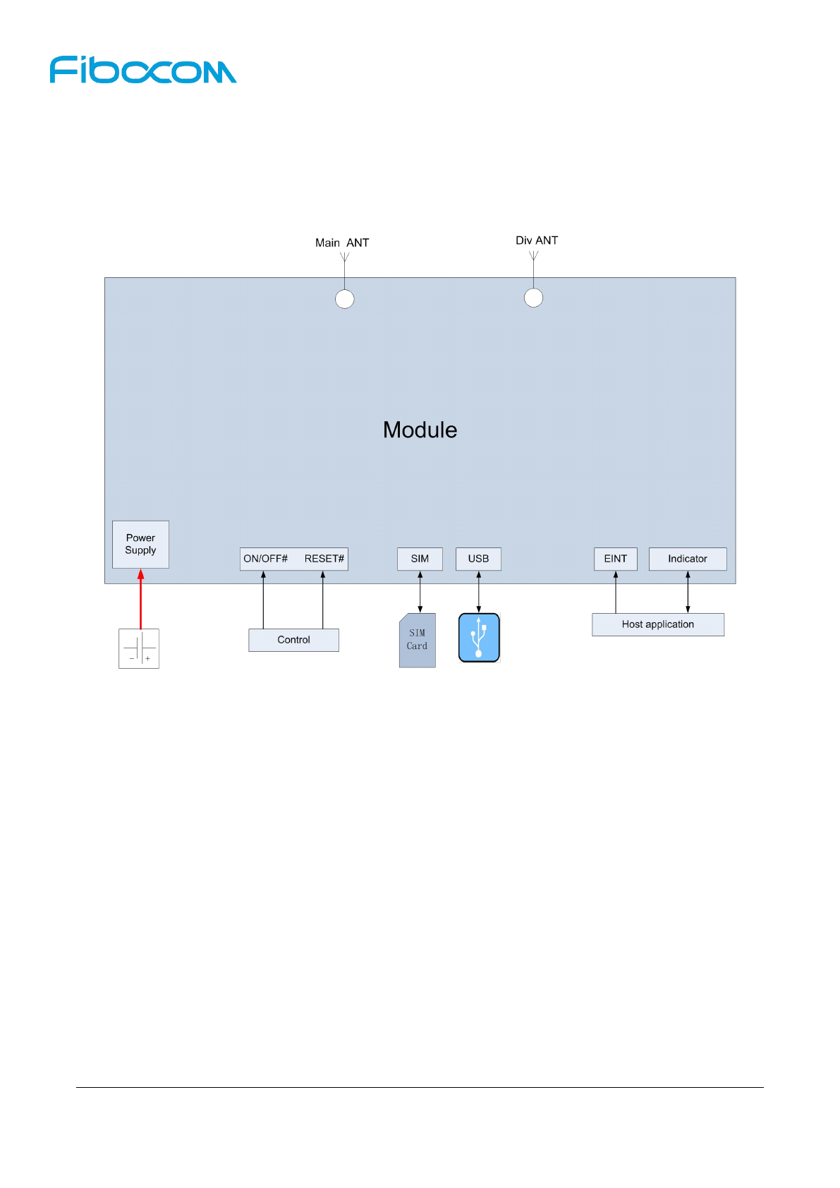
The peripheral application of H380 module is shown in Figure 2-1:
Figure 2-1 Application Framework
2.4 Hardware Framework
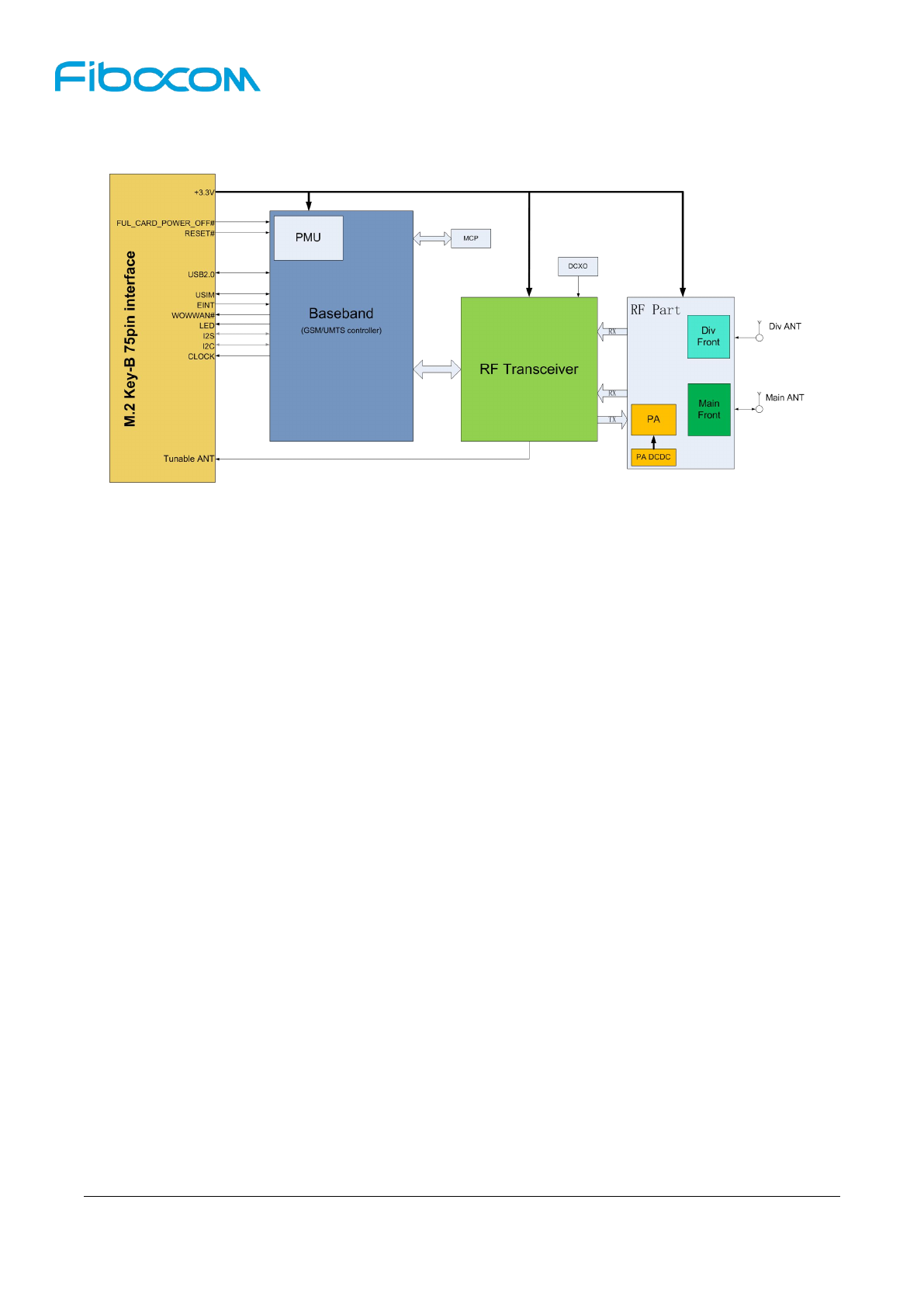
The hardware framework in Figure 2-2 shows the main hardware functions of H380 module, including
baseband and RF functions.
Baseband contains the followings:
GSM/UMTS controller/Power supply
NAND+LPDDR RAM
Application interface
RF contains the followings:
RF Transceiver
RF Power/PA
RF Front end
RF filter
Reproduction forbidden without Fibocom Wireless Inc. written authorization - All Rights Reserved
H380-GL Hardware User Manual Page
12
of
47
Antenna
Figure 2-2 Hardware Framework
3 Application Interface
3.1 M.2 Interface
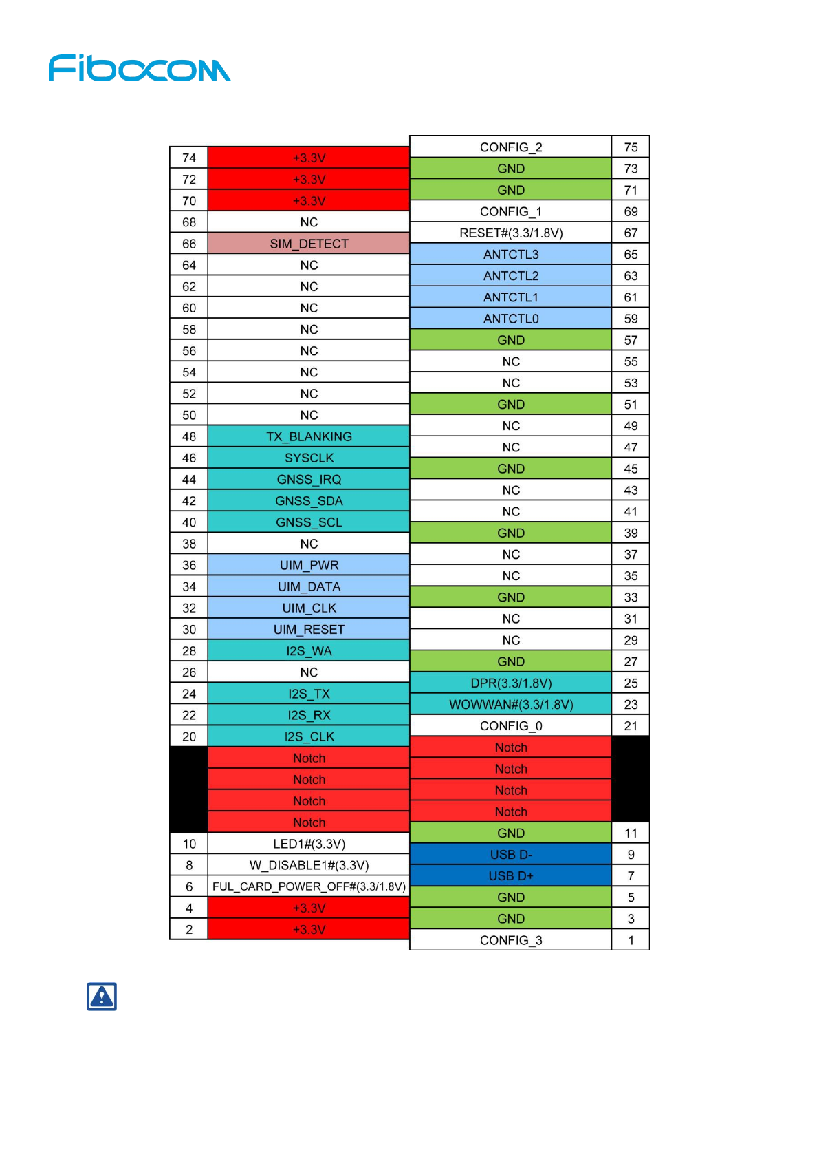
The L816 module adopts the standard M.2 Key-B Interface, with a total of 75 pins.
Reproduction forbidden without Fibocom Wireless Inc. written authorization - All Rights Reserved
H380-GL Hardware User Manual Page
13
of
47
3.1.1 Pin Distribution
Figure 3-1 Pin Distribution Diagram
Note:
Pin “Notch” refers to the notch of the Gold Finger.

Reproduction forbidden without Fibocom Wireless Inc. written authorization - All Rights Reserved
H380-GL Hardware User Manual Page
14
of
47
3.1.2 Pin Definition
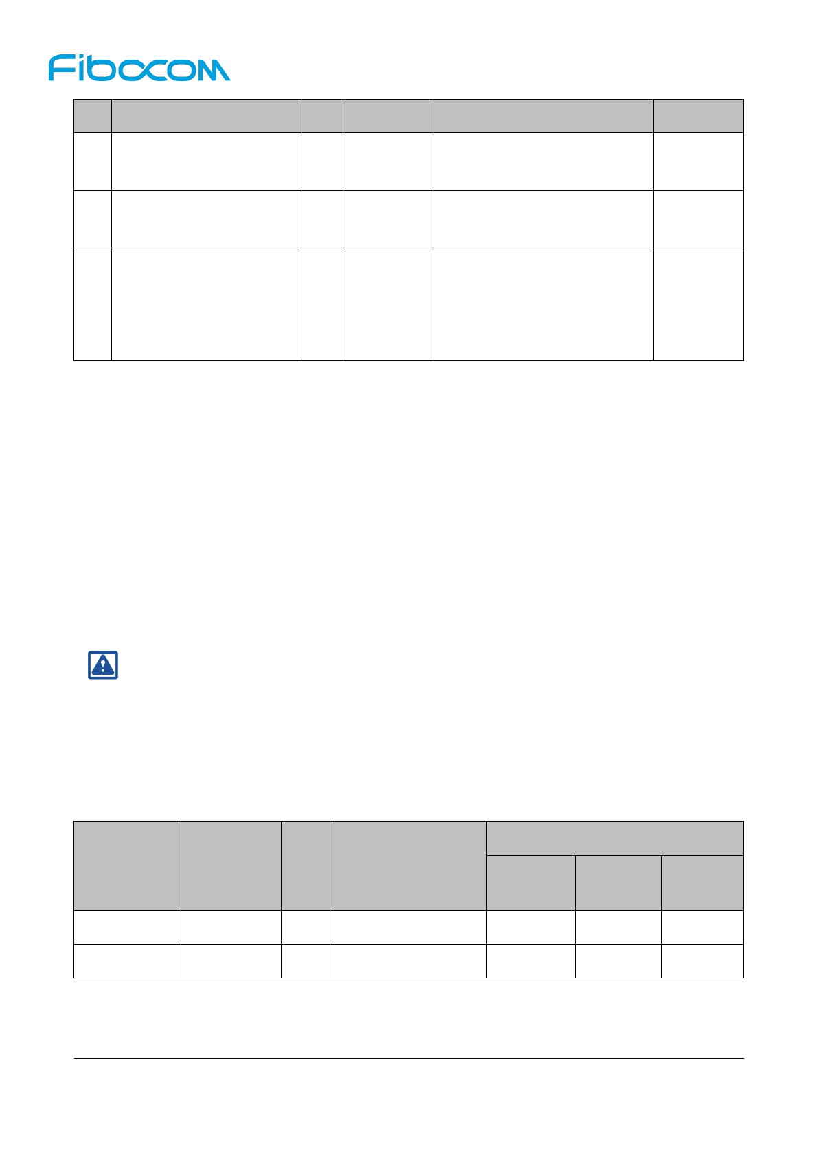
The pin definition is as below:
Pin
Pin Name
I/O
Reset Value
Pin Description
Type
1
CONFIG_3
O
L
Internally connected to GND,
H380 M.2 module configured as
WWAN-SSIC-0 interface type
module
2
+3.3V
PI
Main power input
Power
supply
3
GND
GND
Power
supply
4
+3.3V
PI
Main power input
Power
supply
5
GND
GND
Power
supply
6
FUL_CARD_POWER_OFF
#
I
PU
Start-up and shutdown control
signals, internal 200KΩ pull-up
resistance
CMOS
3.3/1.8V
7
USB D+
I/O
USB 2.0 signal+
0.3---3V
8
W_DISABLE1#
I
PU
WWAN Disable, Internal pull up,
Active low
3.3V/1.8V
9
USB D-
I/O
USB 2.0 signal-
0.3---3V
10
LED1#
O
OD
System status LED, drain output
CMOS 3.3V
11
GND
GND
Power
supply
12
Notch
Notch
13
Notch
Notch
14
Notch
Notch
15
Notch
Notch
16
Notch
Notch
17
Notch
Notch

Reproduction forbidden without Fibocom Wireless Inc. written authorization - All Rights Reserved
H380-GL Hardware User Manual Page
15
of
47
Pin
Pin Name
I/O
Reset Value
Pin Description
Type
18
Notch
Notch
19
Notch
Notch
20
I2S_CLK
O
T
I2S serial clock (not supported)
CMOS 1.8V
21
CONFIG_0
O
Not connected, H380 M.2
module configured as
WWAN-SSIC-0 interface type
module
22
I2S_RX
I
T
I2S serial data input (not
supported)
CMOS 1.8V
23
WOWWAN#
O
L
Module wakes up Host
equipment signal, drain output
CMOS
3.3/1.8V
24
I2S_TX
O
T
I2S serial data output (not
supported)
CMOS 1.8V
25
DPR
I
PU
Body SAR Detect, Internal pull up
CMOS
3.3/1.8V
26
NC
NC
27
GND
GND
Power
supply
28
I2S_WA
O
T
I2S left/right channel clock signal
(not supported)
CMOS 1.8V
29
NC
NC
30
UIM_RESET
O
PP
USIM card reset signal
1.8V/3V
31
NC
NC
32
UIM_CLK
O
PP
USIM card clock signal
1.8V/3V
33
GND
GND
Power
supply
34
UIM_DATA
I/O
PU
USIM card data signal, internal
4.7KΩ pull-up resistance
1.8V/3V
35
NC
NC
36
UIM_PWR
O
USIM card power output
1.8V/3V

Reproduction forbidden without Fibocom Wireless Inc. written authorization - All Rights Reserved
H380-GL Hardware User Manual Page
16
of
47
Pin
Pin Name
I/O
Reset Value
Pin Description
Type
37
NC
NC
38
NC
NC
39
GND
GND
Power
supply
40
GNSS_SCL
O
PU
I2C serial data signal clock,
internal 4.7KΩ pull-up resistance
(not supported)
CMOS 1.8V
41
NC
NC
42
GNSS_SDA
I/O
PU
I2C serial data signal data,
internal 4.7KΩ pull-up resistance
(not supported)
CMOS 1.8V
43
NC
NC
44
GNSS_IRQ
I
PU
Module system switch input
interrupt signal, Internal pull up
CMOS 1.8V
45
GND
GND
Power
supply
46
SYSCLK
O
L
26MHz clock output
1.8V
47
NC
NC
48
TX_BLANKING
O
L
GSM TDMA Timer output signal,
external GPS control signal
CMOS 1.8V
49
NC
NC
50
NC
NC
51
GND
GND
Power
supply
52
NC
NC
53
NC
NC
54
NC
NC
55
NC
NC
56
NC
NC

Reproduction forbidden without Fibocom Wireless Inc. written authorization - All Rights Reserved
H380-GL Hardware User Manual Page
17
of
47
Pin
Pin Name
I/O
Reset Value
Pin Description
Type
57
GND
GND
Power
supply
58
NC
NC
59
ANTCTL0
O
L
Tunable antenna control
signal,bit0 (currently not
supported)
CMOS 1.8V
60
NC
NC
61
ANTCTL1
O
L
Tunable antenna control
signal,bit1 (currently not
supported)
CMOS 1.8V
62
NC
NC
63
ANTCTL2
O
L
Tunable antenna control signal,
bit2 (currently not supported)
CMOS 1.8V
64
NC
NC
65
ANTCTL3
O
L
Tunable antenna control signal,
bit3 (currently not supported)
CMOS 1.8V
66
SIM_DETECT
I
SIM Detect, internal 390KΩ
pull-up resistance
CMOS 1.8V
67
RESET#
I
PU
External reset signal input,
internal 200KΩ pull-up resistance
CMOS
3.3/1.8V
68
NC
NC
69
CONFIG_1
O
L
Internally connected to GND,
H380 M.2 module configured as
WWAN-SSIC-0 interface type
module
70
+3.3V
PI
Main power input
Power
supply
71
GND
GND
Power
supply
72
+3.3V
PI
Main power input
Power
supply
Reproduction forbidden without Fibocom Wireless Inc. written authorization - All Rights Reserved
H380-GL Hardware User Manual Page
18
of
47
Pin
Pin Name
I/O
Reset Value
Pin Description
Type
73
GND
GND
Power
supply
74
+3.3V
PI
Main power input
Power
supply
75
CONFIG_2
O
L
Internally connected to GND,
H380 M.2 module configured as
WWAN-SSIC-0 interface type
module
H: High Voltage Level
L: Low Voltage Level
PD: Pull-Down
PU: Pull-Up
T: Tristate
OD: Open Drain
PP: Push-Pull
PI: Power Input
PO: Power Output
Note:
To ensure that unused pins are floating.
3.2 Power Supply
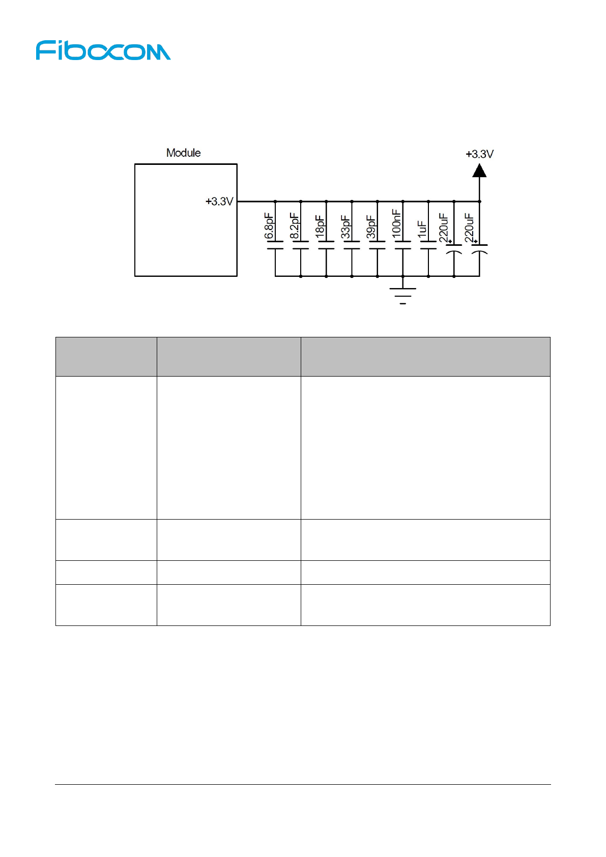
The power interface for H380 module is as follows:
Pin
Pin Name
I/O
Pin Description
DC Parameter (V)
Minimum
Value
Typical
Value
Maximum
Value
2,4,70,72,74
+3.3V
PI
Power input
3.135
3.3
4.4
36
UIM_PWR
PO
USIM power supply
1.8V/3V
Reproduction forbidden without Fibocom Wireless Inc. written authorization - All Rights Reserved
H380-GL Hardware User Manual Page
19
of
47
3.2.1 Power Supply
H380 module provides power supply by using +3.3V pin, and the power supply design is shown in Figure
3-2:
Figure 3-2 Power Supply Design
The filter capacitor design of power supply is as follows:
Recommended
Capacitance
Application
Description
220uF x 2
Voltage-stabilizing
capacitance
To reduce power supply fluctuation in the
operating process of the module, low ESR
capacitance shall be adopted
LDO or DC/DC power supply shall not be less
than 440uF capacitance
Battery power supply can be reduced to
100~220uF capacitance
1uF,100nF
Digital signal noise
Filter the interference produced by clock and
digital signal
39pF,33pF
850,900 MHz band
Filter the RF interference of low band
18pF,8.2pF,6.8pF
1800/1900,2100,2500MHz
band
Filter the RF interference of middle/high band
(including third harmonic of low band)
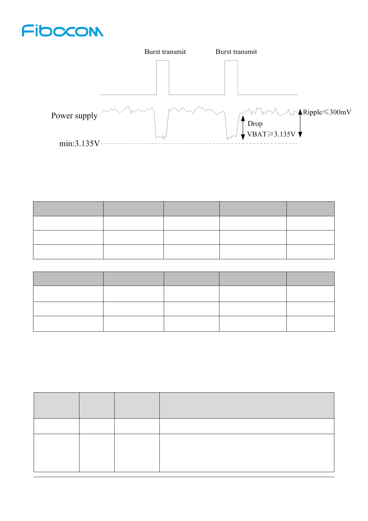
The stable power supply ensures the normal operation of H380 module. In the design, it's should be noted
that the ripple of power supply shall be lower than 300mV. When the module is operating in GSM mode
(Burst transmit), the maximum operating current is up to 2A, and the power supply voltage shall not be
less than 3.135V; otherwise, the module may shut down or restart due to outage. The power supply limit
is shown in Figure 3-3:
Reproduction forbidden without Fibocom Wireless Inc. written authorization - All Rights Reserved
H380-GL Hardware User Manual Page
20
of
47
Figure 3- 3 Power Supply Limit
3.2.2 Logic Level
The 1.8V logic level of H380 module is defined as follows:
Parameter
Minimum Value
Typical Value
Maximum Value
Unit
1.8V logic level
1.71
1.8
1.89
V
VIH
1.3
1.8
1.89
V
VIL
-0.3
0
0.5
V
The 3.3V logic level of H380 module is defined as follows:
Parameter
Minimum Value
Typical Value
Maximum Value
Unit
3.3V logic level
3.135
3.3
3.465
V
VIH
2.3
3.3
3.465
V
VIL
-0.3
0
0.9
V
3.2.3 Power Consumption
When the power supply is 3.3V, the power consumption of H380 module is as below.
The shutdown and sleep currents are as below:
Description
Bands
Average
Current (mA)
Notes/Configuration
Power off
0.07
3.3 V is on and Power_On_Off pin is pulled to low.
HSPA+/
WCDMA
(Standby)
UMTS
supported
bands
2.2
DRX cycle=8 (2.56 s)
Module is registered on and not connected to the 3G
network.

Reproduction forbidden without Fibocom Wireless Inc. written authorization - All Rights Reserved
H380-GL Hardware User Manual Page
21
of
47
Description
Bands
Average
Current (mA)
Notes/Configuration
USB is in suspend.
2.9
DRX cycle=6 (0.64 s)
Module is registered on and not connected to the 3G
network.
USB is in suspend.
GPRS/EDGE
(Standby)
GSM
bands
2.4
MFRMS=5 (1.175 s)
Module is registered on and not connected to the 2G
network.
USB is in suspend.
2.3
MFRMS=2 (0.47 s)
Module is registered on and not connected to the 2G
network.
USB is in suspend.
HSPA+/
WCDMA
(Connect
Standby)
UMTS
bands
3.3
DRX cycle=8 (2.56 s)
Module is registered on the 3G network, and PDP is
activated,
No data transmission. USB is in suspend.
DRX cycle=6 (0.64 s)
Module is registered on the 3G network, and PDP is
activated,
No data transmission. USB is in suspend.
GPRS/EDGE
(Connect
Standby)
GSM
bands
2.6
MFRMS=5 (1.175 s)
Module is registered on the 2G network, and PDP is
activated,
No data transmission. USB is in suspend.
MFRMS=2 (0.47 s)
Module is registered on the 2G network, and PDP is
activated,
No data transmission. USB is in suspend.

Reproduction forbidden without Fibocom Wireless Inc. written authorization - All Rights Reserved
H380-GL Hardware User Manual Page
22
of
47
The power consumption in HSPA/WCDMA mode is as below:
Description
Band
Test Value(mA)
Power
WCDMA
Band 1 (IMT2100)
635
23.5 dBm Tx Power
191
10 dBm Tx Power
150
1 dBm Tx Power
Band 2
(PCS 1900)
653
23.5 dBm Tx Power
182
10 dBm Tx Power
155
1 dBm Tx Power
Band 5
(850 MHz)
529
23.5 dBm Tx Power
185
10 dBm Tx Power
150
1 dBm Tx Power
Band 8
(900 MHz)
561
23.5 dBm Tx Power
176
10 dBm Tx Power
152
1 dBm Tx Power
HSDPA
Band 1 (IMT2100)
176
1 dBm Tx Power
215
10 dBm Tx Power
652
23.5 dBm Tx Power
Band 2
(PCS 1900)
175
1 dBm Tx Power
212
10 dBm Tx Power
634
23.5 dBm Tx Power
Band 5 (850 MHz)
174
1 dBm Tx Power
217
10 dBm Tx Power
678
23.5 dBm Tx Power
Band 8
(900 MHz)
186
1 dBm Tx Power
234
10 dBm Tx Power
679
23.5 dBm Tx Power

Reproduction forbidden without Fibocom Wireless Inc. written authorization - All Rights Reserved
H380-GL Hardware User Manual Page
23
of
47
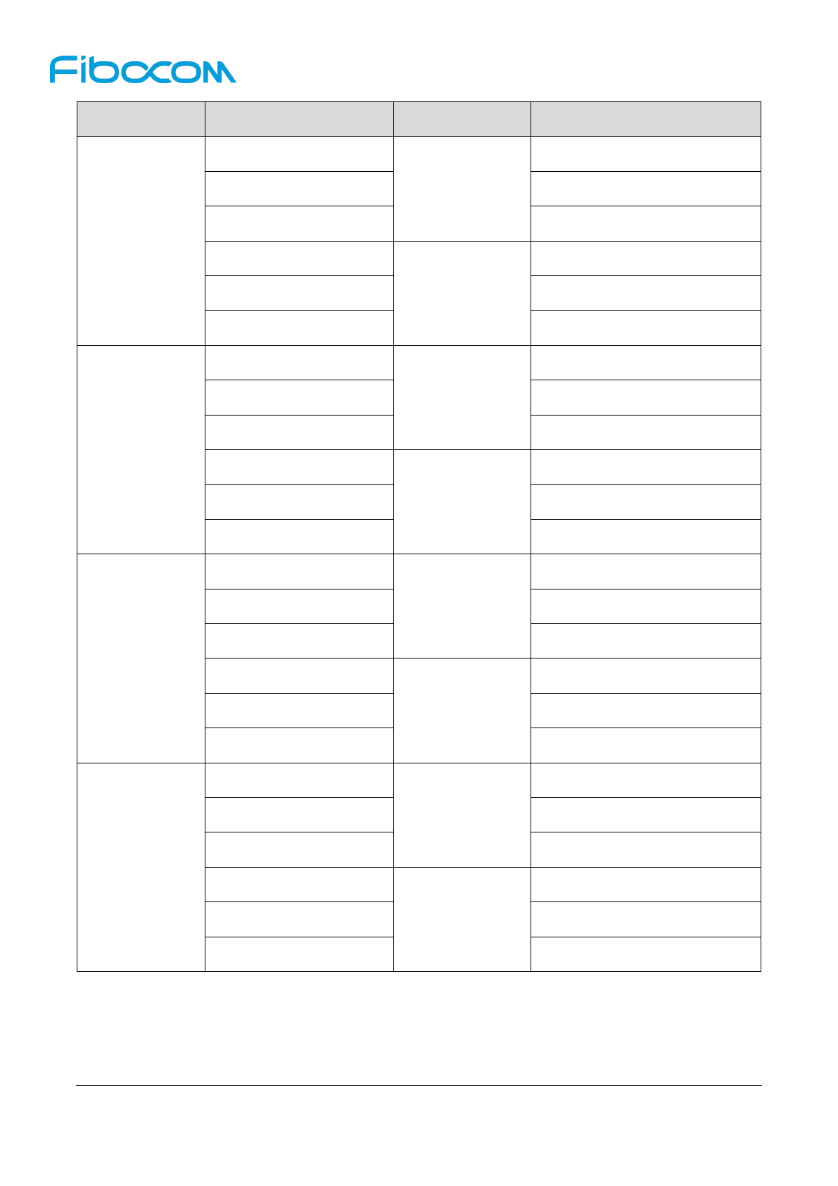
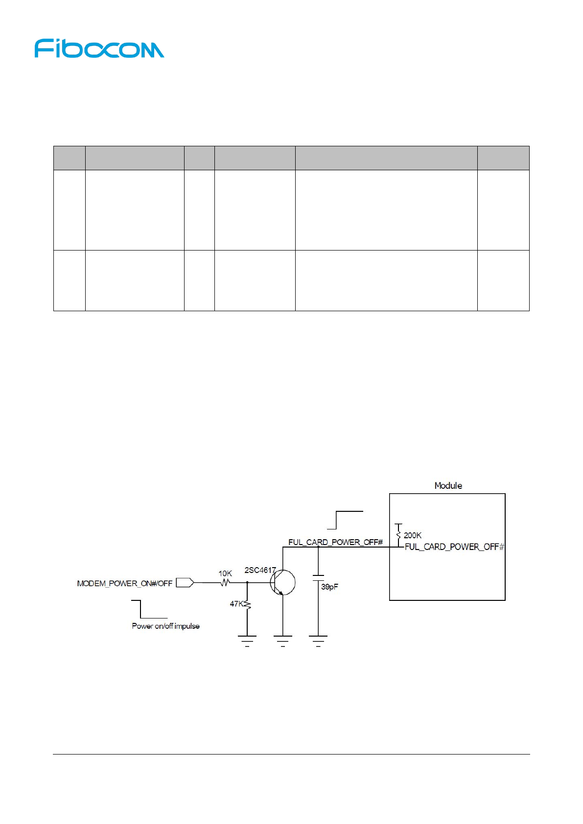
The power consumption in GPRS/EDGE mode is as below:
Description
Test Value 1#
PCL
Configuration
GPRS850
265
5
1 Up/1 Down
353
2 Up/1 Down
399
4 Up/1 Down
99
10
1 Up/1 Down
150
2 Up/1 Down
237
4 Up/1 Down
GPRS900
265
5
1 Up/1 Down
357
2 Up/1 Down
407
4 Up/1 Down
99
10
1 Up/1 Down
154
2 Up/1 Down
238
4 Up/1 Down
GPRS1800
181
0
1 Up/1 Down
239
2 Up/1 Down
278
4 Up/1 Down
65
10
1 Up/1 Down
85
2 Up/1 Down
107
4 Up/1 Down
GPRS1900
179
0
1 Up/1 Down
228
2 Up/1 Down
278
4 Up/1 Down
65
10
1 Up/1 Down
85
2 Up/1 Down
108
4 Up/1 Down
Reproduction forbidden without Fibocom Wireless Inc. written authorization - All Rights Reserved
H380-GL Hardware User Manual Page
24
of
47
Description
Test Value 1#
PCL
Configuration
EDGE850
185
8
1 Up/1 Down
290
2 Up/1 Down
419
4 Up/1 Down
68
15
1 Up/1 Down
90
2 Up/1 Down
125
4 Up/1 Down
EDGE900
185
8
1 Up/1 Down
295
2 Up/1 Down
411
4 Up/1 Down
75
15
1 Up/1 Down
105
2 Up/1 Down
151
4 Up/1 Down
EDGE1800
200
2
1 Up/1 Down
216
2 Up/1 Down
286
4 Up/1 Down
74
10
1 Up/1 Down
96
2 Up/1 Down
117
4 Up/1 Down
EDGE1900
198
2
1 Up/1 Down
213
2 Up/1 Down
290
4 Up/1 Down
73
10
1 Up/1 Down
95
2 Up/1 Down
118
4 Up/1 Down
Reproduction forbidden without Fibocom Wireless Inc. written authorization - All Rights Reserved
H380-GL Hardware User Manual Page
25
of
47
3.3 Control Signal
H380 module provides 2 channel control signals for start-up/shutdown and reset operations of the module,
and the pins are defined as follows:
Pin
Pin Name
I/O
Reset Value
Functions
Type
6
FUL_CARD_POWE
R_OFF#
I
PU
Start-up/shutdown signal, internal
200KΩ pull-up resistance
High level start-up, low level or floating
shutdown
3.3/1.8V
67
RESET#
I
PU
Reset signal, internal 200KΩ pull-up
resistance
Low-active
3.3/1.8V
3.3.1 Module Start-up
3.3.1.1 Start-up Circuit
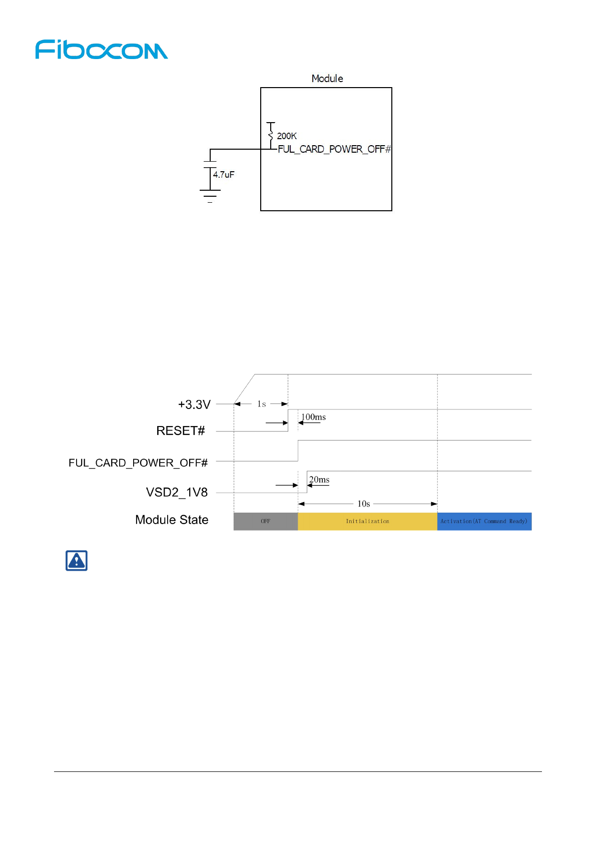
The module start-up pin FUL_CARD_POWER_OFF# requires external pull-up 18.V voltage (VDD_1V8
provided externally), and the module has two start-up modes:
AP (Application Processor) controls the module start-up, and the circuit design is shown in
Figure 3-4:
Automatically start-up when powered on, and the circuit design is shown in Figure 3-5:
Figure 3- 4 Circuit for Module Start-up Controlled by AP
Reproduction forbidden without Fibocom Wireless Inc. written authorization - All Rights Reserved
H380-GL Hardware User Manual Page
26
of
47
Figure 3- 5 Circuit for Automatic Start-up
3.3.1.2 Start-up Timing
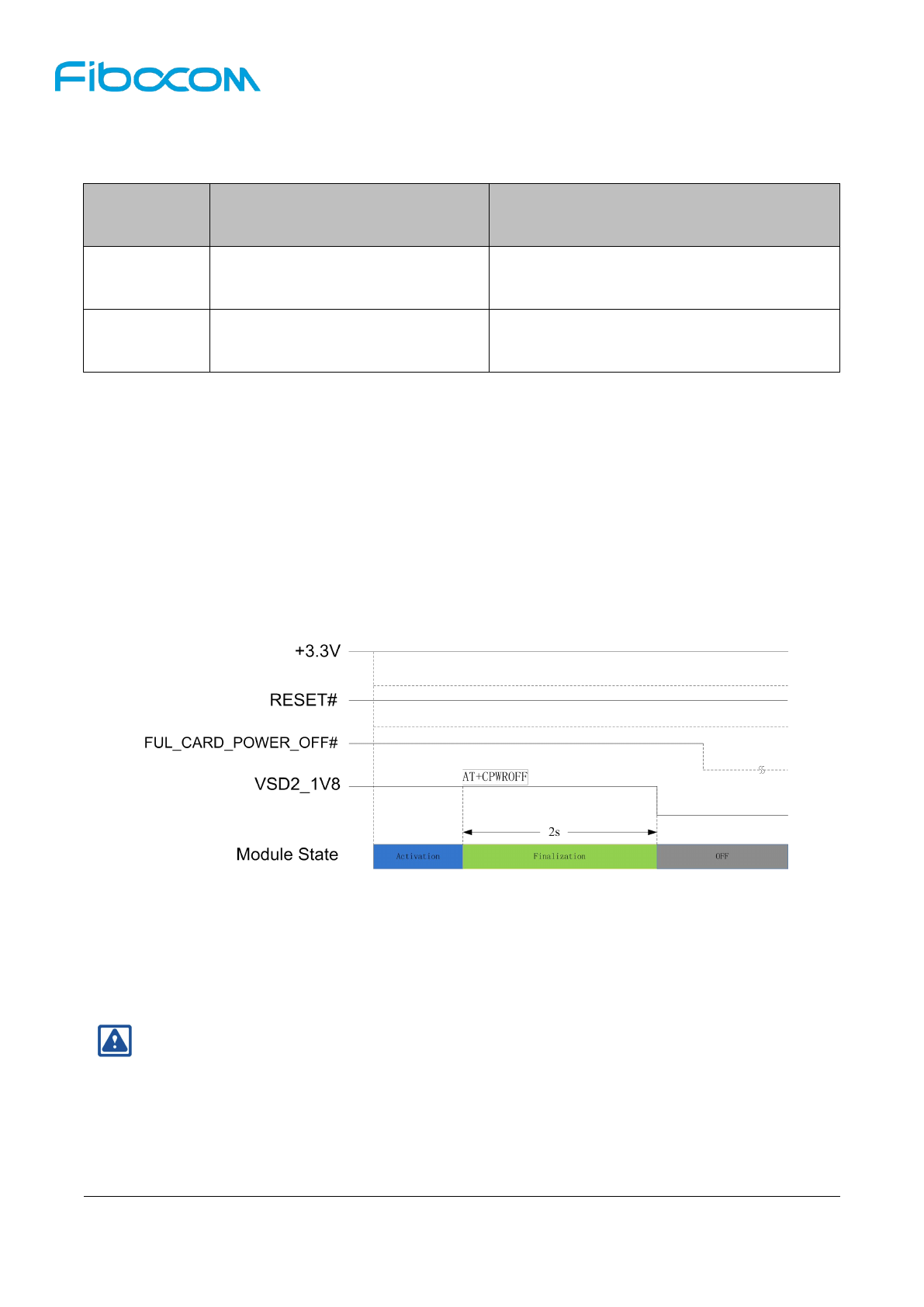
After the module is powered on, when the FUL_CARD_POWER_OFF# signal pulls up and exceeds 20ms
(the recommended value is 100ms), the module starts up. Meanwhile, VSD2_1V8 inside the module
outputs 1.8V voltage, and the module begins the process of start-up initialization. The start-up timing is
shown in Figure 3-6:
Figure 3-6 Start-up Timing Control Diagram
Note:
VSD2_1V8 is a PMU inside the module, it outputs 1.8V voltage and has not been led out via M.2
interface, the appearance of this voltage in timing chart is mainly purposed to facilitate the
understanding of timing;
RESET# is required to delay its pull-up for 1s compared with +3.3V, because the module needs
time for power-on of +3.3V power supply (capacitor charging). If +3.3V maintains as ordinary
power supply, then the delay time is negligible.
Reproduction forbidden without Fibocom Wireless Inc. written authorization - All Rights Reserved
H380-GL Hardware User Manual Page
27
of
47
3.3.2 Module Shutdown
The module supports two shutdown modes as shown below:
Shutdown
Mode
Shutdown Method
Applicable Scenario
Software
shutdown
Send AT+CPWROFF command
Normal shutdown
Hardware
shutdown
Pull down
FUL_CARD_POWER_OFF#
When software shutdown is unavailable in case
of module abnormity
3.3.2.1 Software Shutdown
AT+CPWROFF command can be sent to shut down the module.
When the module receives software shutdown command, the module starts ending process (finalization,
a reverse process of initialization), and the module completes shutdown after about 3s. When ending
process, the module will save the parameters such as network and SIM card in the memory, and then
empty the memory, and switch off PMU power supply. After shutdown, VSD2_1V8 voltage inside the
module will also switch off. The software shutdown timing is shown in Figure 3-7:
Figure 3-7 Software Shutdown Timing Control Diagram
After the completion of software shutdown, FUL_CARD_POWER_OFF# still remains at high level, at this
moment, the module will not start up again. To facilitate the next start-up of the module,
FUL_CARD_POWER_OFF# should be pulled down first.
Note:
VSD2_1V8 is a PMU inside the module, it outputs 1.8V voltage and has not been led out via M.2
interface, the appearance of this voltage in timing chart is mainly purposed to facilitate the
understanding of timing.
Reproduction forbidden without Fibocom Wireless Inc. written authorization - All Rights Reserved
H380-GL Hardware User Manual Page
28
of
47
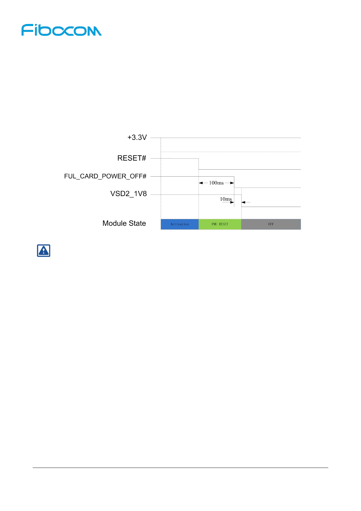
3.3.2.2 Hardware Shutdown
By pulling down FUL_CARD_POWER_OFF# for more than 10ms (the recommended value is 100ms),
the power management unit (PMU) of the module powers down, and then the module achieves hardware
shutdown. The PMU of the module powers down when pulling down FUL_CARD_POWER_OFF#, the
module may be damaged after several start-ups and shutdowns; therefore, RESET# pin shall be pulled
down for 100ms before pulling down FUL_CARD_POWER_OFF#. The hardware shutdown control timing
is shown in Figure 3-8:
Figure 3- 8 Hardware Shutdown Control Timing
Note:
VSD2_1V8 is a PMU inside the module, it outputs 1.8V voltage and has not been led out via M.2
interface, the appearance of this voltage in timing chart is mainly purposed to facilitate the
understanding of timing.
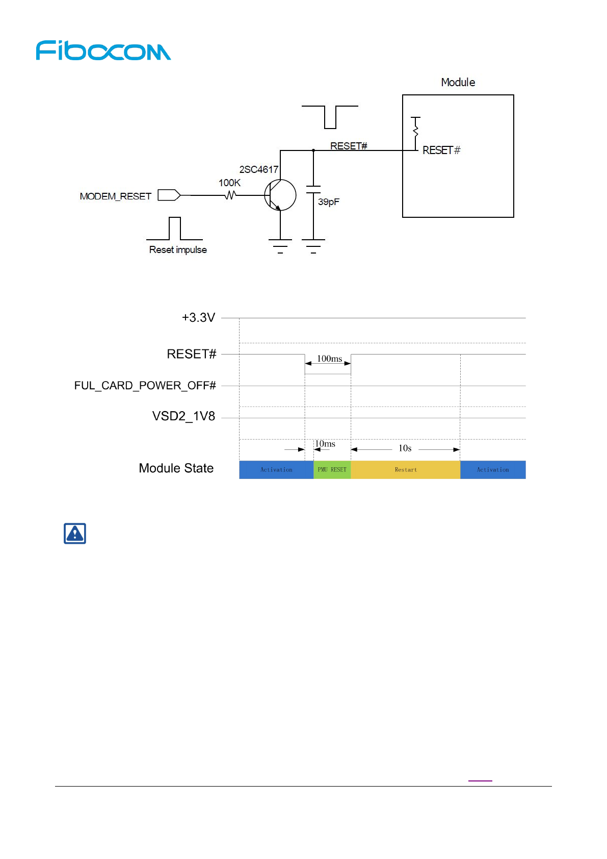
3.3.3 Module Reset
The module supports reset function. Pulling down RESET# signal for more than 10ms (the recommended
value is 100ms) can reset the module to the initial state, and the module restarts after releasing RESET#.
When performing Reset function, PMU inside the module will not power down. The recommended circuit
design is shown in Figure 3-9:
Reproduction forbidden without Fibocom Wireless Inc. written authorization - All Rights Reserved
H380-GL Hardware User Manual Page
29
of
47
Figure 3- 9 Recommended Design of Reset Circuit
The control timing of RESET is shown in Figure 3-10:
Figure 3- 10 Reset Control Timing
Note:
RESET# is a sensitive signal, filter capacitor is recommended to be added close to the module
end. PCB layout shall be away from RF interference and shall have proper grounding handling;
meanwhile, wiring at PCB edge and surface shall be avoided (so as to avoid ESD causing
module reset).
3.4 USB Interface
H380 module supports USB2.0 and is compatible with USB High-Speed (480 Mbits/s) and USB
Full-Speed (12 Mbits/s). Please refer to “Universal Serial Bus Specification 2.0” for timing and electrical
characteristics of the USB of the module.
After inserting H380 module into PC, the USB can map 1 MBIM interface on Win8.1/Win10 system-based
PC and map 7 ACM ports on Android/Linux system-based PC. Please refer to Section 3.7.2 for details of
Reproduction forbidden without Fibocom Wireless Inc. written authorization - All Rights Reserved
H380-GL Hardware User Manual Page
30
of
47
system switching.
MBIM interface is used for initiating data service;
For 7 ACM ports:
1 port is 3G Modem/AT port, which is mainly used for initiating data service
3 ports are used for sending AT Command
1 port is used for capturing software LOG information
2 ports are reserved for future use
3.4.1 USB Interface Definition
Pin
Pin Name
I/O
Reset Value
Pin Description
Type
7
USB_D+
I/O
USB Data Plus
0.3---3V,
USB2.0
9
USB_D-
I/O
USB Data Minus
0.3---3V,
USB2.0
3.4.2 USB2.0 Interface Application
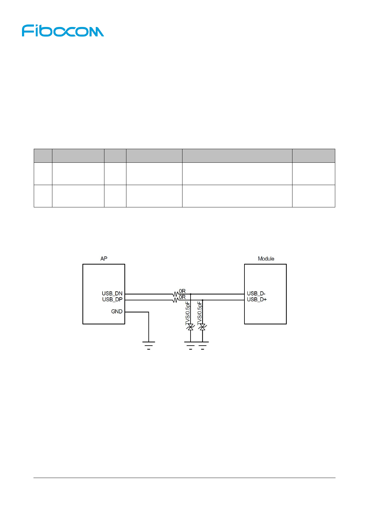
The reference circuit is shown in Figure 3-11:
Figure 3- 11 Reference Circuit for USB2.0 Interface
The module supports USB 2.0 High-Speed, so the TVS equivalent capacitance on USB_D-/D+ differential
signal line shall be lower than 1pF, it’s recommended to adopt TVS with 0.5pF capacitance.
USB_D- and USB_D + are high-speed differential signal lines, the maximum transmission rate is up to
480 Mbits/s, the PCB Layout shall strictly adhere to the following rules:
USB_D- and USB_D+ signal line controls 90 Ω differential impedance;
USB_D- and USB_D+ signal line shall be isometric and parallel, rectangular wiring shall be
avoided;
The cabling of USB_D- and USB_D+ signal line shall be located on the signal layer closest to the
ground, up, down, left and right grounding protections shall be completed for wiring.
Reproduction forbidden without Fibocom Wireless Inc. written authorization - All Rights Reserved
H380-GL Hardware User Manual Page
31
of
47
3.5 USIM Interface
H380 module has built-in USIM card interface that supports 1.8V and 3V SIM card.
3.5.1 USIM Pins
USIM pins are as below:
Pin
Pin Name
I/O
Reset Value
Pin Description
Type
36
UIM_PWR
PO
USIM power supply
1.8V/3V
30
UIM_RESET
O
PP
USIM reset
1.8V/3V
32
UIM_CLK
O
PP
USIM clock
1.8V/3V
34
UIM_DATA
I/O
PU
USIM data, Internal pull up(4.7KΩ)
1.8V/3V
66
SIM_DETECT
I
USIM detect, pull up(390KΩ)
High-active, high level indicates SIM
card inserted, and low level indicates
SIM card removed
1.8V
3.5.2 USIM Interface Circuit
3.5.2.1 N.C. SIM card slot
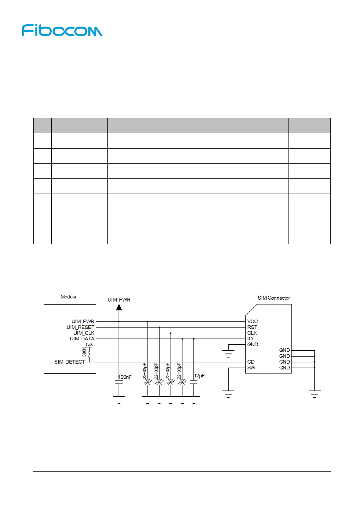
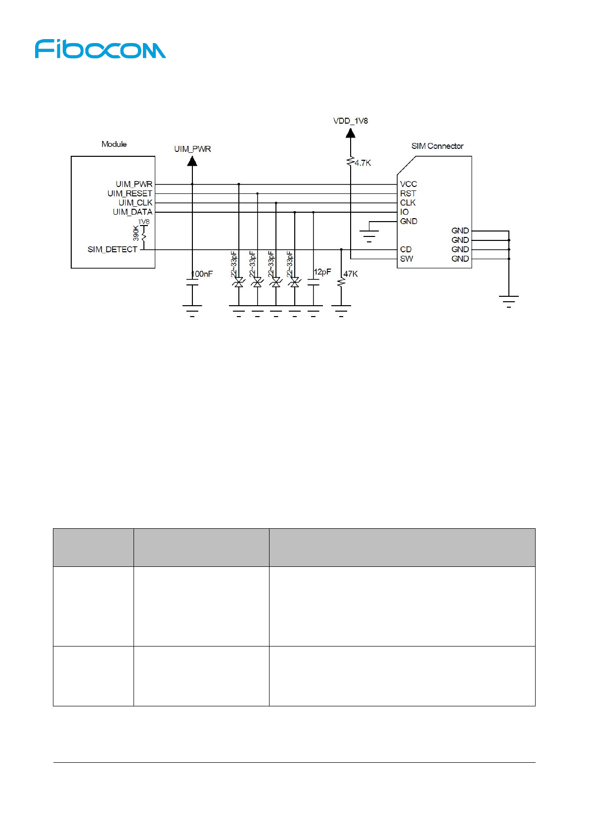
The reference circuit design for the N.C. (Normally Closed) SIM card slot is shown in Figure 3-12:
Figure 3-12 Reference Circuit for N.C. SIM Card Slot
The principle description for N.C. SIM card slot is as follows:
When the SIM card is detached, the CD and SW pins will short, and the SIM_DETECT is low.
When the SIM card is inserted, the CD and SW pins will open, and the SIM_DETECT is high.
Reproduction forbidden without Fibocom Wireless Inc. written authorization - All Rights Reserved
H380-GL Hardware User Manual Page
32
of
47
3.5.2.2 N.O. SIM card slot
The reference circuit design for the N.O. (Normally Open) SIM card slot is shown in Figure 3-13:
Figure 3-13 Reference Circuit for N.O. SIM Card Slot
The principle description for N.O. SIM card slot is shown in the following:
When the SIM card is detached, the CD and SW pins will open, and the SIM_DETECT is low.
When the SIM card is inserted, the CD and SW pins will short, and the SIM_DETECT is high.
3.5.3 USIM Hot-Plugging
H380 supports SIM card hot-plugging function; it judges whether SIM card is inserted or removed by
detecting SIM_DETECT pin state of SIM card slot, so as to support SIM card hot-plugging function.
SIM card hot-plugging function can be configured by “AT+MSMPD” command, and the description of AT
command is as below:
AT Command
Detection of SIM Card
Hot-plugging Function
Function Description
AT+MSMPD=1
On
Default value, SIM card hot-plugging detection function is
on
The module detects whether SIM card is inserted or not
by detecting SIM_DETECT pin state
AT+MSMPD=0
Off
SIM card hot-plugging detection function is off
When start-up, the module reads SIM card and does not
detect SIM_DETECT state
When SIM card hot-plugging detection function is on and SIM_DETECT is at high level, the module
executes SIM card initialization program after detected SIM card inserted, and the module conducts

Reproduction forbidden without Fibocom Wireless Inc. written authorization - All Rights Reserved
H380-GL Hardware User Manual Page
33
of
47
network registration after read SIM card information. When SIM_DETECT is at low level, the module
judges that SIM card has been removed, and then it does not read SIM card.
Note:
SIM_DETECT is high-active by default and can be switched to low-active by AT command.
Please refer to AT command manual for specific AT command.
3.5.4 USIM Design
SIM card circuit design shall meet EMC standard and ESD requirements and shall improve the
anti-interference capability, so as to ensure the stable operation of SIM card. In the design, the followings
shall be strictly complied with:
The layout of SIM card slot shall be as close as possible to the module and away from RF
antenna, DC/DC power supply, clock signal line and other strong interference sources;
SIM card slot with metal shield shall be applied to improve the anti-interference capability;
The cable between the module and SIM card slot shall not be longer than 100mm, as redundant
cable will degrade the quality of signal;
UIM_CLK and UIM_DATA signal shall be isolated by grounding protection, so as to avoid mutual
interference. If impossible, then a grounding protection shall be completed at least for SIM signal
as a group;
The filter capacitor and ESD devices of SIM card signal line shall be placed close to SIM card
slot, and 22~33pF capacitance shall be chose for equivalent capacitance of ESD devices.
3.6 Status Indicator
H380 module provides 3 signals for displaying the operating state of the module, and the status indicator
pins are as below:
Pin
Pin Name
I/O
Reset Value
Pin Description
Type
10
LED1#
O
PD
System status LED, drain output
CMOS 3.3V
23
WOWWAN#
O
L
Module wakes up Host(AP) signal,
drain output
CMOS 3.3/1.8V
48
TX_BLANKING
O
PD
PA Blanking output, external GPS
control signal
CMOS 1.8V
Reproduction forbidden without Fibocom Wireless Inc. written authorization - All Rights Reserved
H380-GL Hardware User Manual Page
34
of
47
3.6.1 LED1# Signal
LED1# signal is used to indicate the operating state of the module, and the detailed description is as
follows:
Operating Mode of
Module
LED1# Signal
RF function is on
Low level (LED light on)
RF function is off
High level (LED light off)
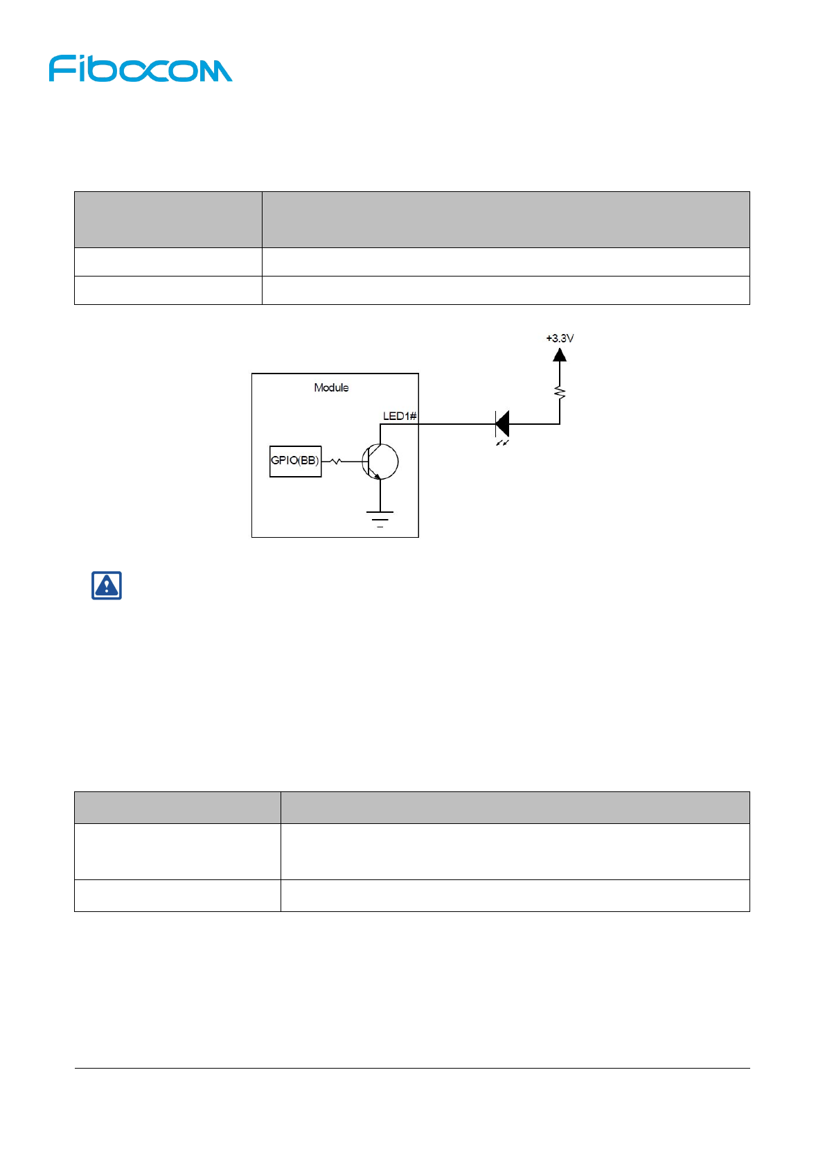
LED drive circuit is shown in Figure 3-15:
Figure 3-15 LED Drive Circuit
Note:
The current-limiting resistance value of LED light is configured according to driving voltage and
driving current of the light.
3.6.2 WOWWAN#
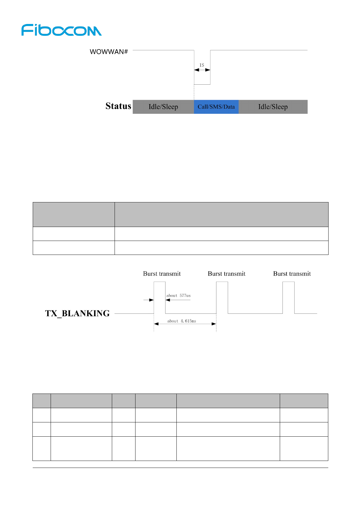
The module wakes up Host (AP) by WOWWAN# signal when receiving incoming call/SMS or data
request. WOWWAN# signal is drain output; therefore, external pull-up is required, WOWWAN# supports
3.3V or 1.8V external voltage pull-up. WOWWAN# signal is defined as follows:
Operating Mode
WOWWAN# Signal
Ringing/SMS or data
requests
An 1s low level pulse by default
Idle/Sleep
High level
WOWWAN# timing is shown in Figure 3-16:
Reproduction forbidden without Fibocom Wireless Inc. written authorization - All Rights Reserved
H380-GL Hardware User Manual Page
35
of
47
Figure 3-16 WOWWAN# Timing
3.6.3 TX_BLANKING
When the module is operating on GSM band, TX_BLANKING outputs pulse signal synchronized with
GSM burst TX timing.
Because GSM TX timing may interfere with GPS signal receiving, the AP switches off GPS or stops GPS
data receiving after detected TX_BLANKING pulse signal, so as to avoid abnormal GPS operation.
Operating Mode of
Module
TX_BLANKING Signal
Default state
Low level
GSM burst TX
Output pulse signal synchronized with GSM burst TX
TX_BLANKING timing is shown in Figure 3-17:
Figure 3-17 TX_BLANKING Timing
3.7 Interrupt Control
H380 module provides 3 interrupt signals, and the pins are defined as below:
Pin
Pin Name
I/O
Reset Value
Pin Description
Type
8
W_DISABLE1#
I
PU
Switch on or off RF network
CMOS 3.3V
25
DPR
I
PU
Body SAR detection
CMOS 1.8V
44
GNSS_IRQ
I
PU
MBIM/ACM interface system
switching
CMOS 1.8V
Reproduction forbidden without Fibocom Wireless Inc. written authorization - All Rights Reserved
H380-GL Hardware User Manual Page
36
of
47
3.7.1 W_DISABLE1#
The module provides hardware for switching on/off WWAN RF function signal, and this function can also
be controlled by AT command. The module enters Flight mode when switching off RF function.
W_DISABLE1# signal function is defined as follows:
W_DISABLE1# Signal
Function
High/Floating
WWAN function is on, the module exits Flight mode
Low
WWAN function is off, the module enters Flight mode
3.7.2 System Switching Control
The module supports switching between MBIM and ACM interfaces, which are respectively designed for
supporting Win8.1/Win10 and Android/Linux/Win7 systems. The detection of interrupt signal GNSS_IRQ
is used for achieving system function switching. GNSS_IRQ signal function is defined as follows:
GNSS_IRQ Signal
Function
High/Floating
Set the USB port of the module as MBIM interface to support
Win8.1/Win10 system
Low
Set the USB port of the module as ACM interface to support
Android/Linux/Win7 system
Note:
When starting up, the module switches MBIM and ACM interfaces by detecting GNSS_IRQ level,
the stability of GNSS_IRQ level shall be maintained in start-up process;
After start-up, the module switches MBIM and ACM interfaces by detecting GNSS_IRQ
rising/falling edge, the filter time is 100ms. When the condition is met, the module will restart and
switch to another interface.
3.7.3 BODY SAR
H380 module supports BODY SAR function through DPR pin detection. DPR is at high level by
default, the AP pulls down the DPR when approaching human body is detected by using SAR Sensor
(distance sensor), then the module reduces the transmit power to a preset threshold value, decreasing
RF radiation on the human body. The preset threshold value can be set by the relevant AT command or
DPR Tool. DPR function is defined as follows:
DPR Signal
Function
High/Floating
The module maintains default transmit power
Low
Reduce the threshold value of maximum transmit power of the module
Reproduction forbidden without Fibocom Wireless Inc. written authorization - All Rights Reserved
H380-GL Hardware User Manual Page
37
of
47
3.8 Clock Interface
H380 module supports 1 channel clock and can respectively output 26MHz clock.
Pin
Pin Name
I/O
Reset Value
Pin Description
Type
46
SYSCLK
O
26M clock output
(available for external GPS or Audio
Codec)
1.8V
3.9 Config Interface
H380 module provides 4 config pins and is configured as WWAN-SSIC-0 type M.2 module:
Pin
Pin Name
I/O
Reset Value
Pin Description
Type
1
CONFIG_3
O
L
Internally connected to GND
21
CONFIG_0
O
NC
69
CONFIG_1
O
L
Internally connected to GND
75
CONFIG_2
O
L
Internally connected to GND
M.2 module configuration is as follows:
Config_0
(pin21)
Config_1
(pin69)
Config_2
(pin75)
Config_3
(pin1)
Module Type and Main
Host Interface
Port
Configuration
NC
GND
GND
GND
WWAN-SSIC
0
Please refer to “PCI Express M.2 Specification Rev0.9-3” for details.
3.10 Other Interfaces
The ANT Tunable interface of the module is currently not supported.
Reproduction forbidden without Fibocom Wireless Inc. written authorization - All Rights Reserved
H380-GL Hardware User Manual Page
38
of
47
4 RF Interface
4.1 RF Interface
4.1.1 RF Interface Function
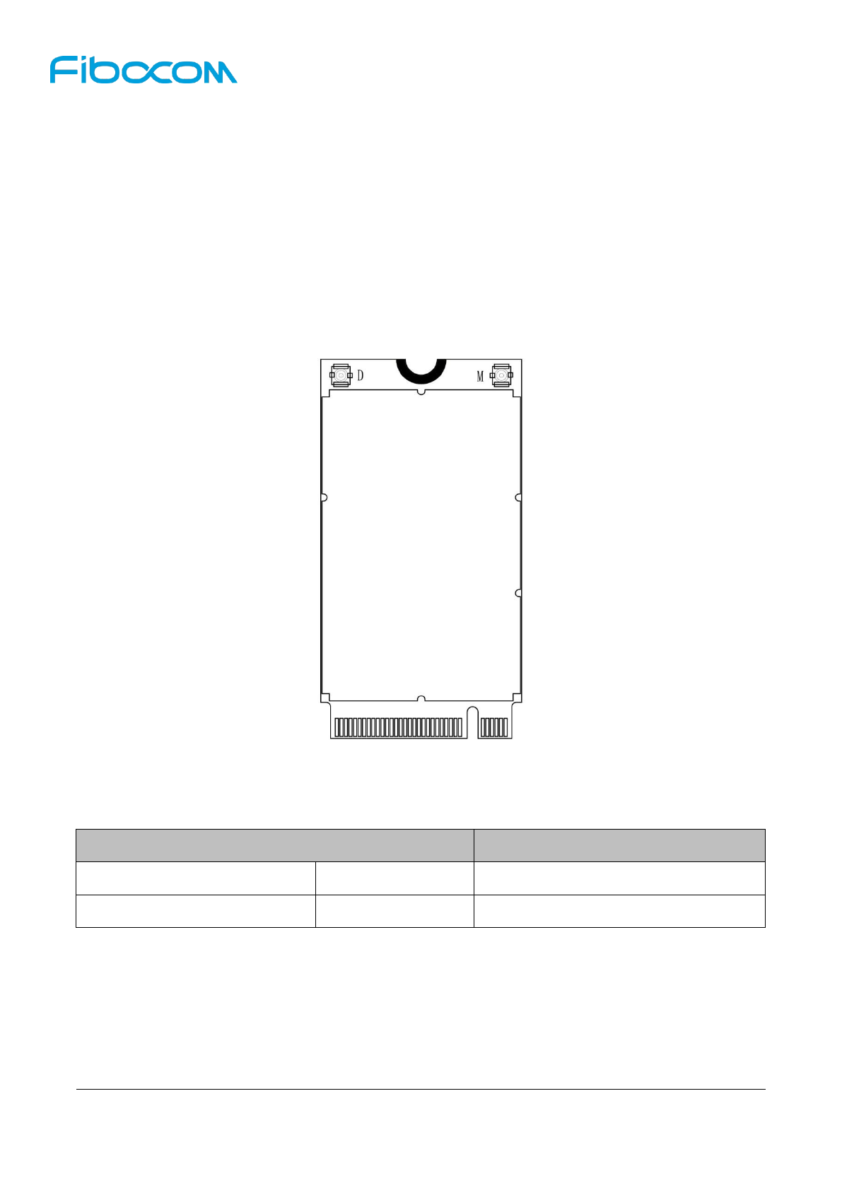
H380 module provides 2 RF connectors for connecting with external antennas. As shown in Figure
4-1, “M” refers to RF main antenna, which is used for sending and receiving RF signals; “D” refers to
Diversity antenna, which is used for receiving diversity RF signals.
Figure 4-1 Schematic Diagram of RF Interface
4.1.2 RF Connector Performance
Rated Conditions
Environmental Conditions
Frequency Range
DC to 6GHz
Temperature Range:
Characteristic Impedance
50Ω
–40°C to +85°C
4.1.3 RF Connector Dimension
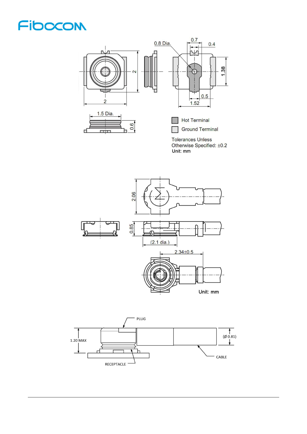
H380 module applies standard M.2 module RF connector, the model is Murata MM4829-2702, and
the dimension of connector is 2*2*0.6mm. The dimension of connector is as below:
Reproduction forbidden without Fibocom Wireless Inc. written authorization - All Rights Reserved
H380-GL Hardware User Manual Page
39
of
47
Figure 4-2 Dimension Figure of RF Connector
Figure 4-3 Dimension Figure of 0.81mm Coaxial Line Coupling with RF Connector
Figure 4-4 Schematic Diagram of 0.81mm Coaxial Line Locking into RF Connector
Reproduction forbidden without Fibocom Wireless Inc. written authorization - All Rights Reserved
H380-GL Hardware User Manual Page
40
of
47
4.2 Operating Band
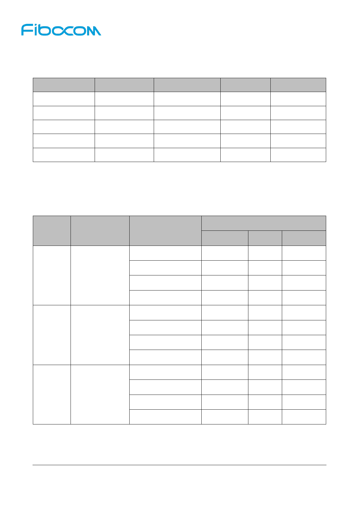
The operating band of H380 module antenna is as below:
Operating Band
Description
Mode
Tx (MHz)
Rx (MHz)
Band 1
IMT 2100MHz
WCDMA
1920 - 1980
2110 - 2170
Band 2
PCS 1900MHz
WCDMA/GSM
1850 - 1910
1930 - 1990
Band 3
DCS 1800MHz
GSM
1710 - 1785
1805 - 1880
Band 5
CLR 850MHz
WCDMA/GSM
824 - 849
869 - 894
Band 8
E-GSM 900MHz
WCDMA/GSM
880 - 915
925 - 960
4.3 Transmitting Power
The transmitting power of various bands of H380 module is as below:
Mode
Condition
Band
Transmit Power (dBm)
Min
Type
Max
GSM
GMSK
(1TX Slot)
GSM850
31.5
32.5
33.5
GSM900
31.5
32.5
33.5
DCS1800
28.5
29.5
30.5
PCS1900
28.5
29.5
30.5
EGPRS
8PSK
(1TX Slot)
GSM850
26
27
28
GSM900
26
27
28
DCS1800
25
26
27
PCS1900
25
26
27
WCDMA
I
22.5
23.5
24.5
II
22.5
23.5
24.5
V
22.5
23.5
24.5
VIII
22.5
23.5
24.5
Reproduction forbidden without Fibocom Wireless Inc. written authorization - All Rights Reserved
H380-GL Hardware User Manual Page
41
of
47
4.4 Receiving Sensibility
The sensitivity of various bands of H380 module is as below:
Mode
Band
Rx Sensitivity (dBm)
Conditions
Typ
Max
GPRS
GSM850
-112.5
-109
GMSK
(CS1,BLER<10%)
GSM900
-112
-109
DCS1800
-112.5
-109
PCS1900
-112
-109
EGPRS
GSM850
-104.5
-101.5
8PSK
(MCS5,BLER<10%)
GSM900
-104
-101
DCS1800
-104.5
-101.5
PCS1900
-104.5
-101.5
WCDMA
(Main)
I
-110
-108
(BER<0.1%)
II
-110.5
-108
V
-110.5
-108
VIII
-110
-108
WCDMA
(Diversity)
I
-110.5
-108
(BER<0.1%)
II
-110
-108
V
-111
-108
VIII
-111
-108

Reproduction forbidden without Fibocom Wireless Inc. written authorization - All Rights Reserved
H380-GL Hardware User Manual Page
42
of
47
4.5 Antenna Design
H380 module provides two antenna connectors, i.e., main and diversity antenna connectors, and the
design requirements of antenna is as below:
Requirements of H380 Module Main Antenna
Frequency range
The most appropriate antenna shall be used to adapt to the relevant bands
Bandwidth
(GSM/EDGE)
GSM850: 70 MHz
GSM900: 80 MHz
GSM1800(DCS): 170 MHz
GSM1900(PCS): 140 MHz
Bandwidth (WCDMA)
WCDMA band I(2100): 250 MHz
WCDMA band II(1900): 140 MHz
WCDMA band V(850): 70 MHz
WCDMA band VIII(900): 80 MHz
Impedance
50Ω
Input power
> 33dBm(2 W) peak power GSM
> 23.5dBm average power WCDMA
Standing-wave ratio
(SWR) recommended
≤ 2:1
5 Structure Specification
5.1 Product Appearance
The product appearance for the H380 module is shown in Figure 5-1:
Figure 5-1 Top View & Bottom View
Reproduction forbidden without Fibocom Wireless Inc. written authorization - All Rights Reserved
H380-GL Hardware User Manual Page
43
of
47
5.2 Dimension of Structure
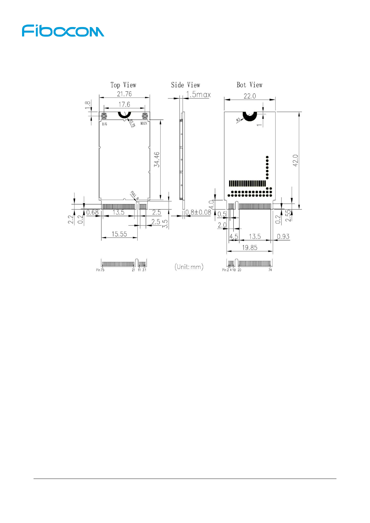
The dimension of structure of H380 module is shown in Figure 5-2:
Figure 5-2 Dimension of Structure
5.3 M.2 Interface Type
H380 M.2 module applies 75-pin Gold Finger as the external interface, of which 67 pins are signal
interfaces, and 8 pins are a notch (as shown in Figure 3-1). Please refer to the description in Section 5.2
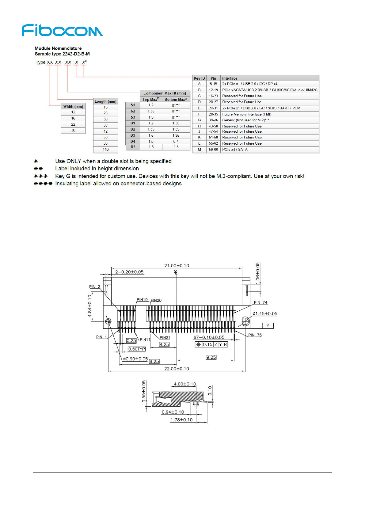
for dimension of the module. According to the definition of M.2 interface, H380 module applies Type
2242-S3-B interface (22x42mm, the thickness of element layer on Top surface is up to 1.5mm, the
thickness of PCB is 0.8mm, and Key ID is B).
Reproduction forbidden without Fibocom Wireless Inc. written authorization - All Rights Reserved
H380-GL Hardware User Manual Page
44
of
47
5.4 M.2 Connector
H380 module connects with the AP by using M.2 connector, LOTES M.2 connector is recommended,
the model is APCI0026-P001A, as shown in Figure 5-3. Please refer to specification design for connector
package.
Figure 5-3 Dimension of M.2 Connector

Reproduction forbidden without Fibocom Wireless Inc. written authorization - All Rights Reserved
H380-GL Hardware User Manual Page
45
of
47
5.5 Storage
5.5.1 Storage Life
Storage conditions (recommended): Temperature: 23±5°C, relative humidity (RH): 35-70%.
Storage period (sealed vacuum packing): 12 months under the recommended storage conditions.
5.6 Package
The H380 module uses the tray sealed vacuum packing, combined with the hard cartoon box outer
packing method, so that the storage, transportation and the usage of the module can be protected to the
greatest extent.
Note:
The vacuum package bag includes the humidity card and a desiccant. The module is the
humidity sensitive device, and the humidity sensitivity level is Class 3, which meets the
requirements of the American Electronic Component Industry Association (JEDEC). Please
protect the module to avoid the permanent damage to the product caused by humidity.
The module is a sophisticated electronic product and may suffer permanent damage if no proper
ESD protection measures are taken.
5.6.1 Tray Package
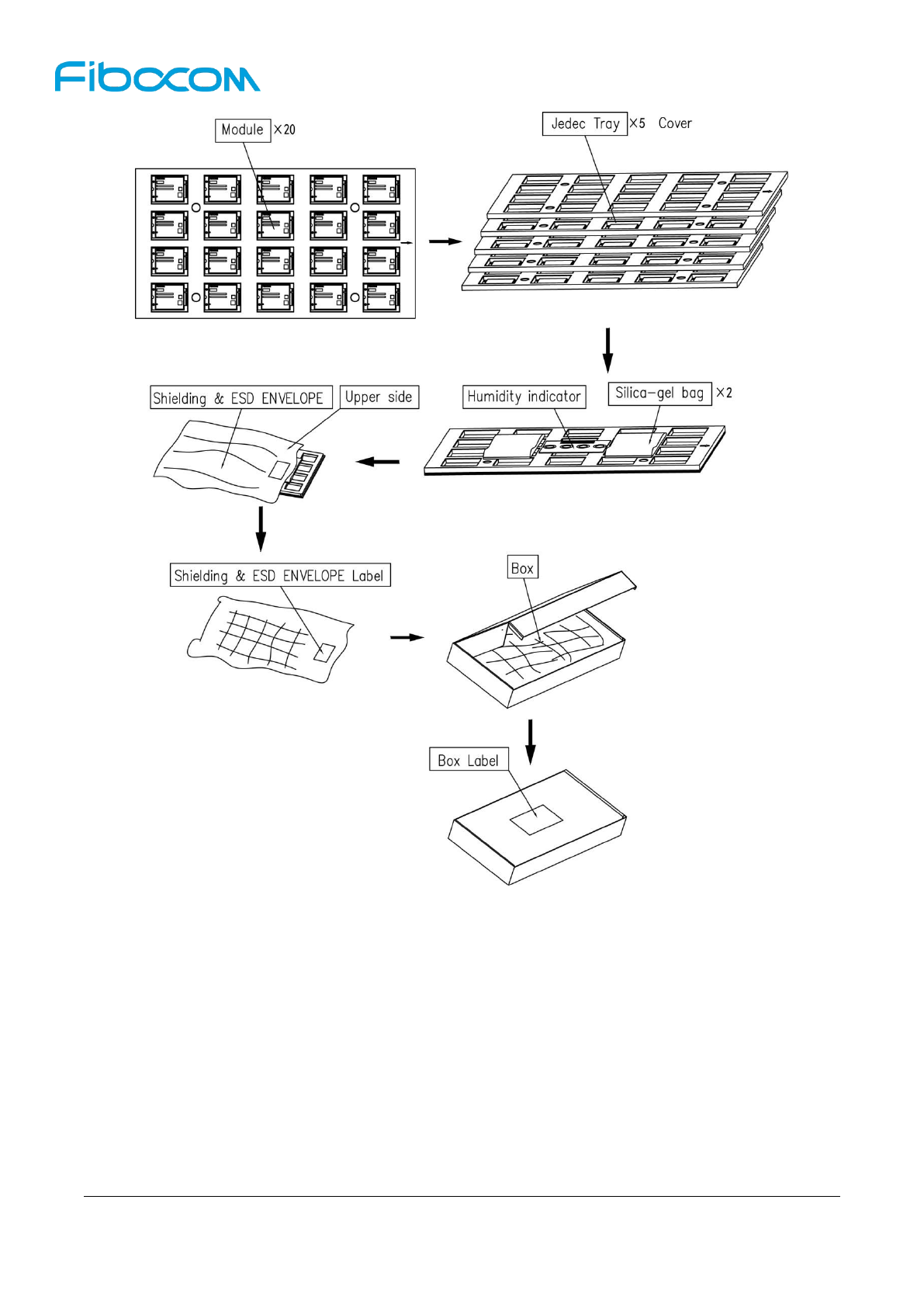
The L816 module uses tray package, 20pcs are packed in each tray, with 5 trays in each box and 6
boxes in one case. Tray packing process is shown in Figure 5-4:
Reproduction forbidden without Fibocom Wireless Inc. written authorization - All Rights Reserved
H380-GL Hardware User Manual Page
46
of
47
Figure 5-4 Tray Packing Process
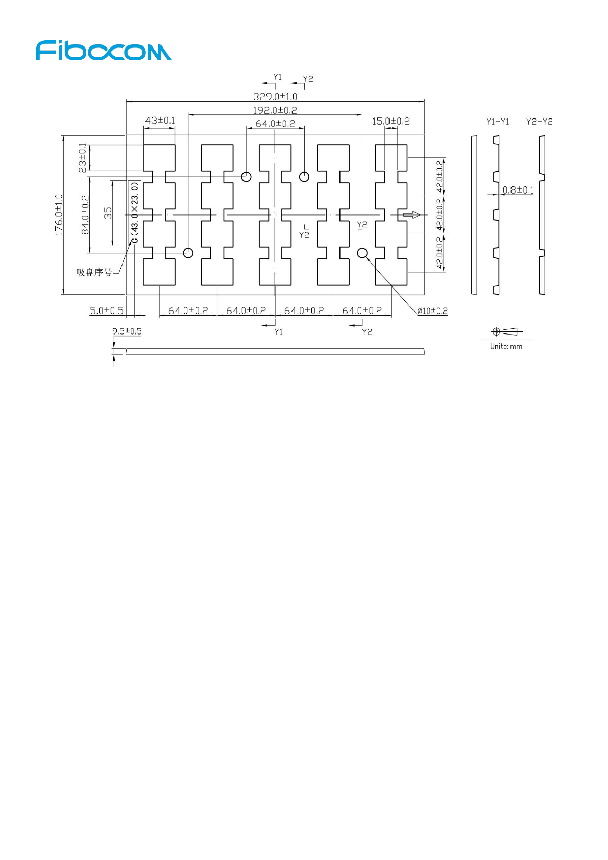
5.6.2 Tray Size
The type of tray is C (43*23mm), and its size is 329*176*9.5mm, as shown in Figure 5-5:
Reproduction forbidden without Fibocom Wireless Inc. written authorization - All Rights Reserved
H380-GL Hardware User Manual Page
47
of
47
Figure 5-5 Tray Size