Fibocom Wireless L831 LTE Module User Manual ng
Fibocom Wireless Inc. LTE Module ng
User Manual

ng
L831-EA Module Hardware
User Manual
Version: V1.0.1
Date: 2015-02-12

L831-EA Module Hardware User Manual Page
2
of
43
Confidential Material
This document contains information highly confidential to Fibocom Wireless Inc. (Fibocom). Fibocom
offers this information as a service to its customers, to support application and engineering efforts that use
the products designed by Fibocom. The information provided is based upon requirements specifically
provided to Fibocom by the customers. All specifications supplied herein are subject to change.
Disclosure of this information to other parties is prohibited without the written consent of Fibocom.
Copyright
Copy, Reproduce, Distribute and/or Edit of this document or part of it as well as utilization of its contents
and communication thereof to others without express authorization are prohibited. Offenders will be held
liable for payment of damages. All rights created by patent grant or registration of a utility model or design
patent are reserved. Copyright ©2015 Fibocom Wireless Inc. All rights reserved.
Trademarks Notice
The FIBOCOM Logo is registered by Fibocom Wireless Inc. All other product or service names or logos
are the property of their respective owners. Copyright ©2015 Fibocom Wireless Inc. All rights reserved.

L831-EA Module Hardware User Manual Page
3
of
43
FOR FCC
Federal Communications Commission (FCC) Declaration of Conformity
This device complies with part 15 of the FCC Rules. Operation is subject to the following two conditions:
(1) This device may not cause harmful interference, and (2) this device must accept any interference
received, including interference that may cause undesired operation.
This device has been tested and found to comply with the limits for a Class B digital , pursuant to Part 15
of the FCC Rules. These limits are designed to provide reasonable protection against harmful
interference in a residential installation. This equipment generates, uses and can radiated radio frequency
energy and, if not installed and used in accordance with the instructions, may cause harmful interference
to radio communications. However, there is no guarantee that interference will not occur in a particular
installation If this equipment does cause harmful interference to radio or television reception, which can
be determined by turning the equipment off and on, the user is encouraged to try to correct the
interference by one or more of the following measures:
-Reorient or relocate the receiving antenna.
-Increase the separation between the equipment and receiver.
-Connect the equipment into an outlet on a circuit different from that to which the receiver is connected.
-Consult the dealer or an experienced radio/TV technician for help.
FCC Caution:
Changes or modifications not expressly approved by the party responsible for compliance could void the
user‘s authority to operate the equipment.
RF Exposure Information
This device meets the government’s requirements for exposure to radio waves.
This device is designed and manufactured not to exceed the emission limits for exposure to radio
frequency (RF) energy set by the Federal Communications Commission of the U.S. Government.
This device complies with FCC radiation exposure limits set forth for an uncontrolled environment. In
order to avoid the possibility of exceeding the FCC radio frequency exposure limits, human proximity to
the antenna shall not be less than 20cm (8 inches) during normal operation.

L831-EA Module Hardware User Manual Page
4
of
43
IMPORTANT NOTE:
This module is intended for OEM integrator. The OEM integrator is still responsible for the FCC
compliance requirement of the end product, which integrates this module. 20cm minimum distance has to
be able to be maintained between the antenna and the users for the host this module is integrated into.
Under such configuration, the FCC radiation exposure limits set forth for an population/uncontrolled
environment can be satisfied.
Any changes or modifications not expressly approved by the manufacturer could void the user's authority
to operate this equipment.
USERS MANUAL OF THE END PRODUCT:
In the users manual of the end product, the end user has to be informed to keep at least 20cm separation
with the antenna while this end product is installed and operated. The end user has to be informed that
the FCC radio-frequency exposure guidelines for an uncontrolled environment can be satisfied. The end
user has to also be informed that any changes or modifications not expressly approved by the
manufacturer could void the user's authority to operate this equipment. If the size of the end product is
smaller than 8x10cm, then additional FCC part 15.19 statement is required to be available in the users
manual: This device complies with Part 15 of FCC rules. Operation is subject to the following two
conditions: (1) this device may not cause harmful interference and (2) this device must accept any
interference received, including interference that may cause undesired operation.
LABEL OF THE END PRODUCT:
The final end product must be labeled in a visible area with the following " Contains TX FCC ID:
ZMOL831". If the size of the end product is larger than 8x10cm, then the following FCC part 15.19
statement has to also be available on the label: This device complies with Part 15 of FCC rules.
Operation is subject to the following two conditions: (1) this device may not cause harmful interference
and (2) this device must accept any interference received, including interference that may cause
undesired operation.
L831-EA Module Hardware User Manual Page
5
of
43
Revision History
Version
Date
Remarks
V1.0.0
2014-12-30
Initial version
V1.0.1
2015-02-12
Update the consumption and the power on/off timing
L831-EA Module Hardware User Manual Page
6
of
43
Applicability Table
No.
Type
Note
1
L831-EA
The difference of L831-EA wireless module as listed below:
Model Type
LTE FDD
WCDMA
GSM/GPRS/EDGE
L831-EA
Band
1,2,3,4,5,7,8,13,17,
18,19,20
Band 1,2,4,5,8
850/900/1800/1900MHz

L831-EA Module Hardware User Manual Page
7
of
43
Contents
IMPORTANT NOTE:................................................................................................................................................... 4
1 Preface..................................................................................................................................................................... 10
1.1 Outline........................................................................................................................................................... 10
1.2 Standards..................................................................................................................................................... 10
2 Introduction.............................................................................................................................................................. 12
2.1 Description................................................................................................................................................... 12
2.2 Specifications...............................................................................................................................................12
2.3 Appearance.................................................................................................................................................. 15
3 Mechanical...............................................................................................................................................................16
3.1 Dimension.....................................................................................................................................................16
3.2 Application Interface Description..............................................................................................................17
3.3 M.2 Connector............................................................................................................................................. 18
4 Hardware Overview................................................................................................................................................19
4.1 Pins Definition..............................................................................................................................................19
4.1.1 Pins Number.....................................................................................................................................19
4.1.2 Pins Description............................................................................................................................... 20
5 Hardware Interface.................................................................................................................................................24
5.1 Power Interface........................................................................................................................................... 24
5.1.1 Power Supply................................................................................................................................... 24
5.1.2 VSD2_1V8........................................................................................................................................ 24
5.2 Power on/off and Reset Signal................................................................................................................. 25
5.2.1 Power on/off Signal......................................................................................................................... 25
5.2.1.1 Power on................................................................................................................................25
5.2.1.2 Power off................................................................................................................................25
5.2.1.3 Recommended Circuit Design of Power on/off signals................................................. 26
5.2.2 RESET Signal.................................................................................................................................. 27
5.3 Index Signal................................................................................................................................................. 28
5.3.1 Index Signal Pins............................................................................................................................. 28
5.4 USB Interface...............................................................................................................................................28
5.4.1 Definition of USB Interface.............................................................................................................28
5.4.2 Application for USB Interface........................................................................................................ 29
5.5 USIM Interface.............................................................................................................................................29

L831-EA Module Hardware User Manual Page
8
of
43
5.5.1 USIM Pins......................................................................................................................................... 30
5.5.2 Description of USIM........................................................................................................................ 30
5.5.2.1 “Normally Closed”SIM Circuit Design............................................................................ 30
5.5.2.2 “Normally Open” SIM Circuit Design.................................................................................31
5.5.3 USIM Design Points........................................................................................................................ 31
5.5.4 USIM Hot Plug..................................................................................................................................32
5.5.4.1 Hardware Connection..........................................................................................................32
5.5.4.2 Software Configuration........................................................................................................32
5.6 Digital Audio................................................................................................................................................. 32
5.6.1 Description of I2S Interface............................................................................................................33
5.6.2 Description of PCM Interface.........................................................................................................33
5.7 Android/Win8Dual System Switch Control Interface.............................................................................34
5.8 W_DISABLE# Interface............................................................................................................................. 34
5.8.1 Description of WWAN_DISABLE# Interface...............................................................................34
5.8.2 Description of GPS_DISABLE# Interface................................................................................... 35
5.9 TX_BLANKING Interface........................................................................................................................... 35
5.10 The WAKEUP_HOST Interface..............................................................................................................35
5.11 BODY_SAR Interface............................................................................................................................... 36
5.12 Description of I2C Interface.................................................................................................................... 36
5.13 Clock Interface.......................................................................................................................................... 36
5.14 Config Interface......................................................................................................................................... 36
5.15 RF Interface............................................................................................................................................... 37
5.15.1 Description of RF Connector....................................................................................................... 37
5.15.2 Description of RF Connecting Seat............................................................................................37
5.15.3 Main Performance of RF Connector.......................................................................................... 38
5.16 Other Interfaces........................................................................................................................................ 39
6 Electrical and Environmental................................................................................................................................ 40
6.1 Electrical....................................................................................................................................................... 40
6.2 Environmental..............................................................................................................................................40
7 RF Interface............................................................................................................................................................. 41
7.1 Operating Band........................................................................................................................................... 41
7.1.1 Antenna Band...................................................................................................................................41
7.2 RF PCB Design........................................................................................................................................... 41
7.2.1 Routing Principle..............................................................................................................................41

L831-EA Module Hardware User Manual Page
9
of
43
7.2.2 Impedance Design...........................................................................................................................42
7.3 Antenna Design........................................................................................................................................... 42
7.3.1 Antenna Design Requirements..................................................................................................... 42

L831-EA Module Hardware User Manual Page
10
of
43
1 Preface
1.1 Outline
The document outlines the electrical, RF performance, mechanical size and application environment of
L831-EA wireless module. Under the help of the document and others application notice, the application
developer could understand quickly the performance of L831-EA series wireless module, and developing
the product.
1.2 Standards
The products `reference design standard as listed below:
3GPP TS 27.007 -v6.9.0: AT command set for User Equipment (UE)
3GPP TS 27.005 -v6.0.1: Use of Data Terminal Equipment -Data Circuit terminating Equipment
(DTE-DCE) interface for Short Message Service (SMS) and Cell Broadcast Service (CBS)
3GPP TS 23.040 -v6.9.0: Technical realization of Short Message Service (SMS)
3GPP TS 24.011 -v6.1.0: Point- to - Point (PP) Short Message Service (SMS) support on mobile
radio interface
3GPP TS 27.010 -v6.0.0: Terminal Equipment to User Equipment (TE-UE) multiplexer protocol
3GPP TS 27.060 -v6.0.0: Packet domain; Mobile Station (MS) supporting Packet Switched services
3GPP TS 25.304-v6.10.0: User Equipment (UE) procedures in idle mode and procedures for cell
reselection in connected mode
3GPP TS 25.308 -v6.4.0: High Speed Downlink Packet Access (HSDPA); Overall description;
Stage 2
3GPP TS 25.309 -v6.6.0: FDD enhanced uplink; Overall description; Stage 2
3GPP TS 23.038 -v6.1.0: Alphabets and language - specific information
3GPP TS 21.111 -v6.3.0: USIM and IC card requirements
3GPP TS 31.111 -v6.11.0 "USIM Application Toolkit (USAT)"
3GPP TS 45.002 -v6.12.0: Multiplexing and multiple access on the radio path
3GPP TS 51.014 -v4.5.0: Specification of the SIM Application Toolkit for the Subscriber Identity
Module - Mobile Equipment (SIM-ME) interface
3GPP TS 51.010 -1 -v6.7.0: Mobile Station (MS) conformance specification; Part 1: Conformance
specification
3GPP TS 22.004 -v6.0.0: General on supplementary services

L831-EA Module Hardware User Manual Page
11
of
43
3GPP TS 23.090 -v6.1.0: Unstructured Supplementary Service Data (USSD); Stage 2
3GPP TS 24.008 v6.19, Mobile radio interface Layer 3 specification;
3GPP TS 25.101 V7.18.0: User Equipment (UE) radio transmission and reception (FDD)
3GPP TS 36.101 V9.18.0: User Equipment (UE) radio transmission and reception
3GPP TS 36.104 V9.13.0: Base Station (BS) radio transmission and reception
3GPP TS 36.106 V9.4.0: FDD Repeater radio transmission and reception
3GPP TS 36.113 V9.5.0: Base Station (BS) and repeater ElectroMagnetic Compatibility (EMC)
3GPP TS 36.124 V9.2.0: ElectroMagnetic Compatibility (EMC) requirements for mobile terminals
and ancillary equipment
3GPP TS 36.133 V9.18.0: Requirements for support of radio resource management
3GPP TS 34.121-1 version 7.2.0: The requirements and this test apply to all types of UTRA for the
FDD UE
3GPP TS 36.521-1 User Equipment (UE) conformance specification; Radio transmission and
reception; Part 1: Conformance testing
3GPP TS 34.122 V5.7.0: Technical Specification Group Radio Access Network; Radio transmission
and reception (TDD)
3GPP TS 45.005 9.4.0: Digital cellular telecommunications system (Phase 2+);Radio transmission
and reception
L831-EA Module Hardware User Manual Page
12
of
43
2 Introduction
2.1 Description
L831-EA modules are highly integrated LTE M.2 wireless communication modules, supports 3 module 12
band and the global main 4G/3G/2G modes (LTE FDD/WCDMA/GSM) These bands support the mobile
operators `cellular network of the Europe & Asia-Pacific and American marketing.
2.2 Specifications
Specifications
Bands
L831-EA
LTE FDD: Band 1,2,3,4,5,7,8,13,17,18,19,20
WCDMA HSPA+: Band 1,2,4,5,8
GSM/GPRS/EDGE: 850/900/1800/1900MHz
Data
LTE FDD
Category 4 (150Mbps DL,50Mbps UL)
UMTS/HSDPA/HSUPA
3GPP Rel.8
DC-HSDPA 42Mbps(Cat24)/42Mbps(Cat20)
HSUPA 11.5Mbps(Cat7)
GSM 3GPP release 7
EDGE (E-GPRS) multi-slot class 33(296kbps DL,
236.8kbps UL)
GPRS multi-slot class 33 (107kbps DL,85.6kbps UL)
Physical
Dimension : 32mm x 42mm x 2.3 mm
Interface : M.2
Weight : 5.9 grams
Environment
Operating Temperature: -30℃~ +55℃
Storage Temperature: -40℃~ +85℃
Performance
Operating Voltage
Voltage:3.135V ~ 4.4V Normal:3.3V
Operating Current
(Typical Value)
5.5mA (Sleep Mode)
3G Idle:16mA
LTE FDD Idle: 17mA
LTE FDD DATA:700mA
WCDMA Talk:580mA
L831-EA Module Hardware User Manual Page
13
of
43
2G Talk:300mA (GSM PCL5)
Interfaces
RF Interface
Antenna : Mainx1,Diversityx1
Function Interface
1 x USB 2.0,Multiple Profiles over USB
SIM Support,I2C Support,I2S/PCM Support
GPIO,Clock
Data Features
Protocol Stack
Embedded TCP/IP and UDP/IP protocol stack
EDGE
Multi-slot class 33 (5 Down; 4 Up; 6 Total)
Coding Scheme MCS1~9
GPRS
Multi-slot class 33 (5 Down; 4 Up; 6 Total)
Coding Scheme MCS1~4
CSD
UMTS(14.4kbps),GSM(9.6kbps)
USSD
Support
SMS
MO / MT Text and PDU modes
Cell broadcast
Audio
Digital Audio
Voice coders :EFR/HR/FR/AMR
VoLTE (not support yet)
Audio Control
Gain control
Character Set
IRA,GSM,UCS2,HEX
AT commands
FIBOCOM proprietary AT commands
GSM 07.05
GSM 07.07
Accessories
Firmware Loader Tool over USB
User Manual
Developer Kit
L831-EA Module Hardware User Manual Page
14
of
43
Note:
1. Please make sure the temperature for device will not be higher than 55˚C.
2. The minimum distance between the user and/or any bystander and the radiating structure of the
transmitter is 20cm.
3. Assessment of compliance of the product with the requirements relating to the Radio and
Telecommunication Terminal Equipment Directive (EC Directive 1999/5/EC) was performed by
PHOENIX TESTLAB (Notified Body No.0700),
L831-EA Module Hardware User Manual Page
15
of
43
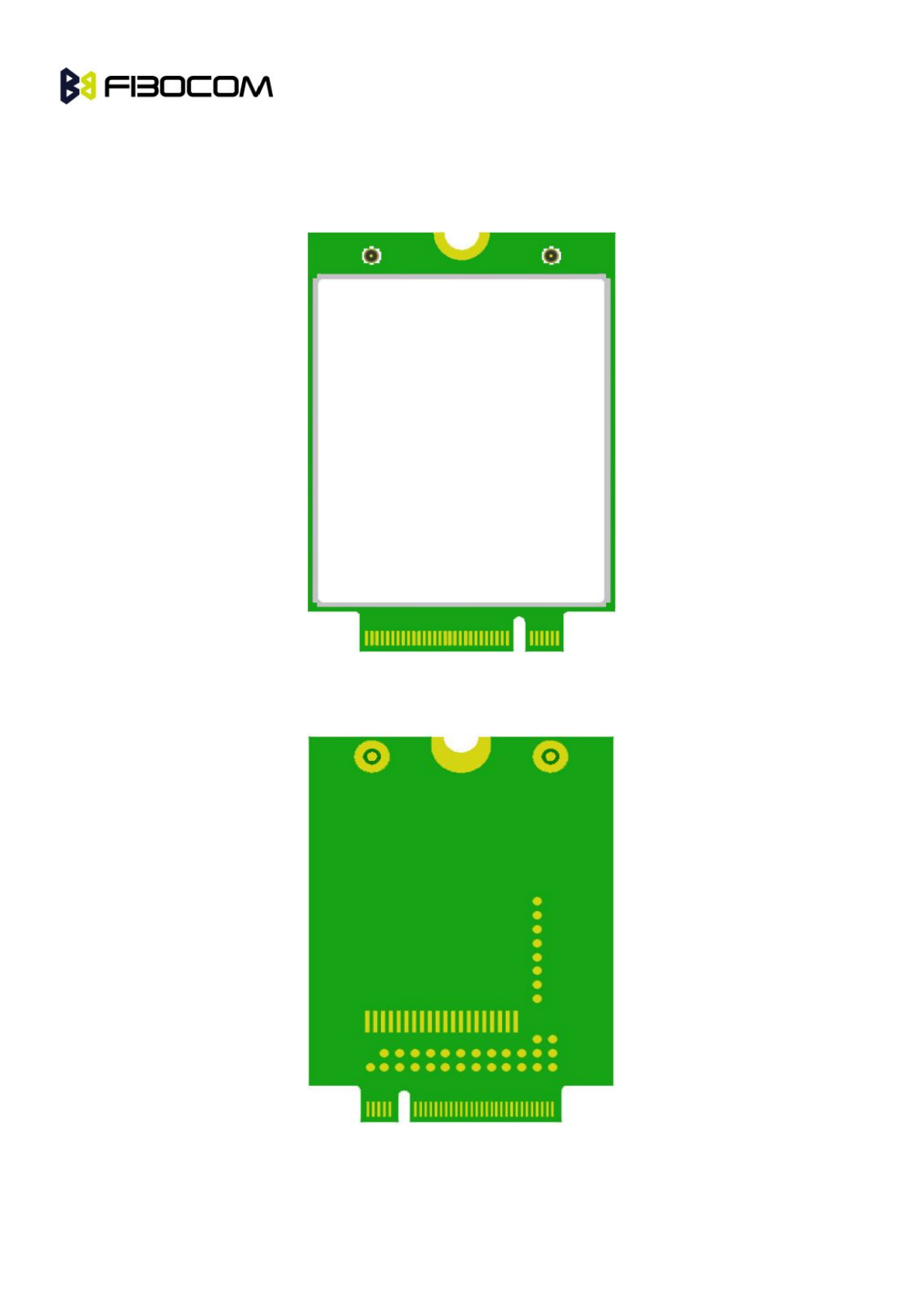
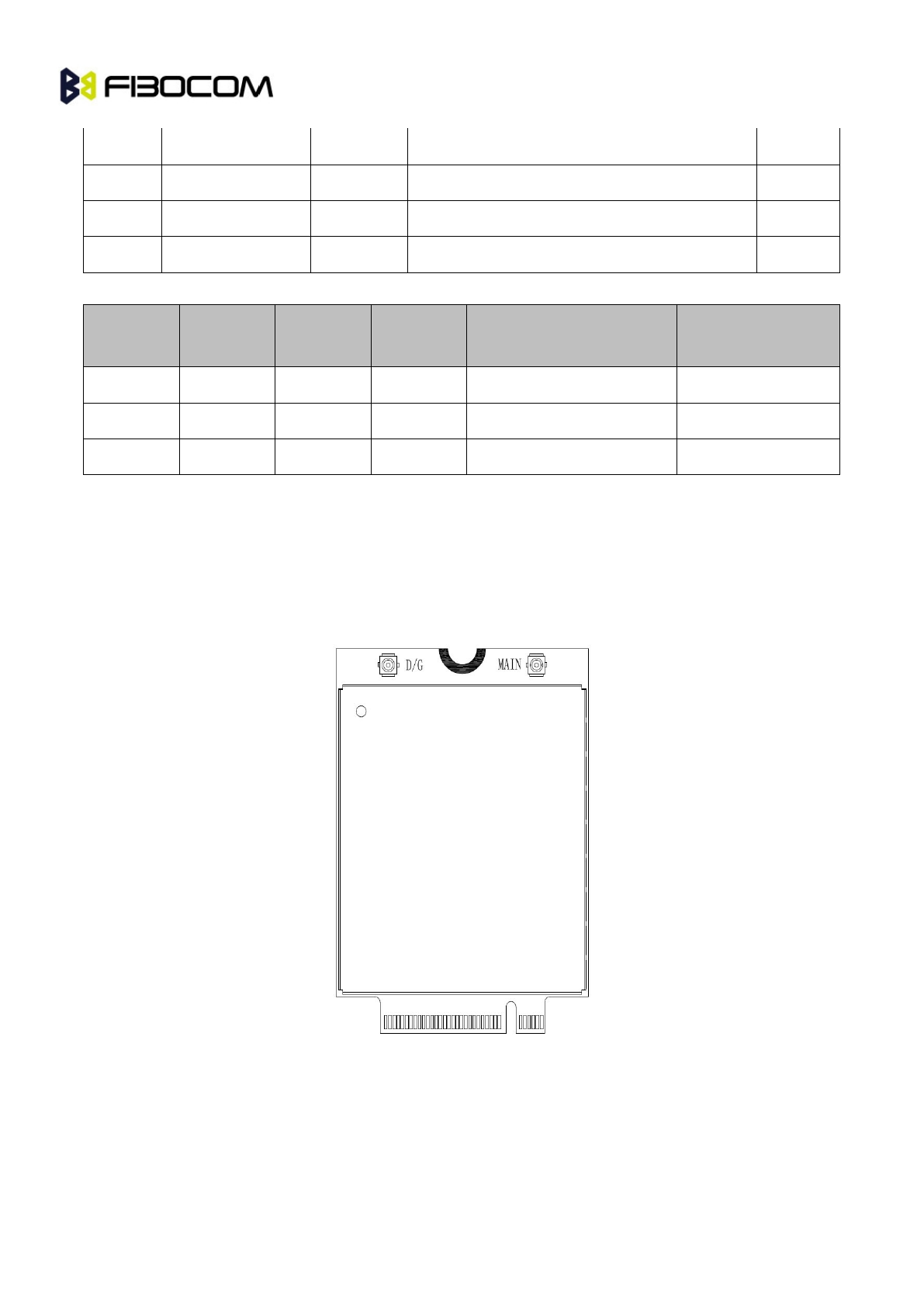
2.3 Appearance
The following pictures show the L831-EA wireless module.
Top view:
Figure 2- 1 Top View
Bottom view:
Figure 2- 2 Bottom View
L831-EA Module Hardware User Manual Page
16
of
43
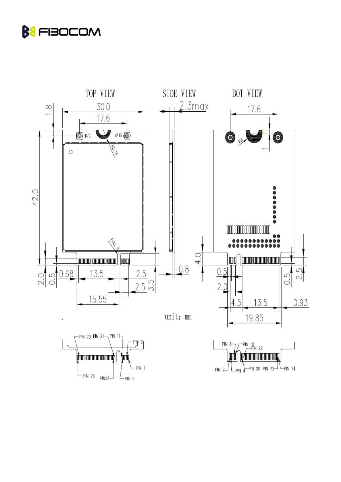
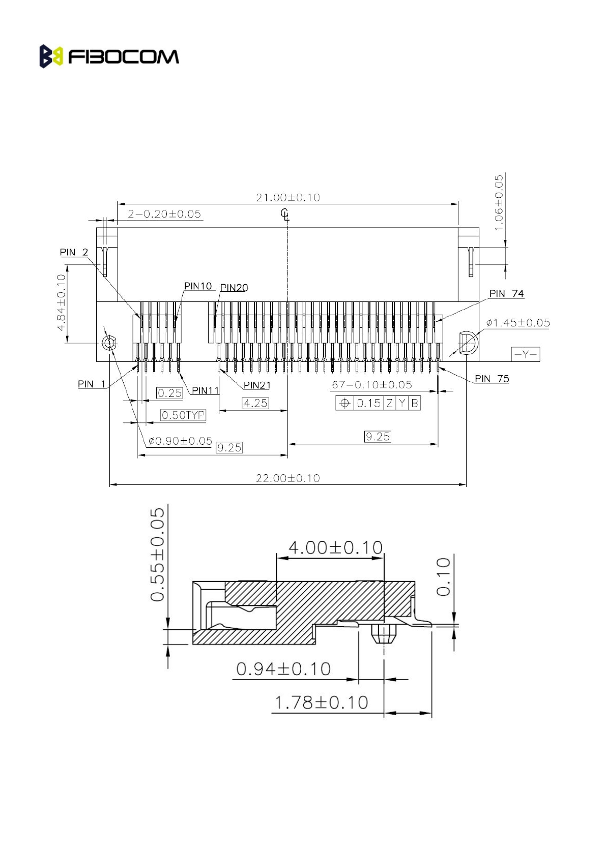
3 Mechanical
3.1 Dimension
Figure3- 1Dimension Diagram
L831-EA Module Hardware User Manual Page
17
of
43
3.2 Application Interface Description
L831-EA module uses 75-pin gold fingers as the external interface, the size of the module please refer to
the section3.1.
As shown in Figure 4-2, L831-EA module uses the 75-pin fingers interface (67pin is the signal interface
and Pin8 is notch).
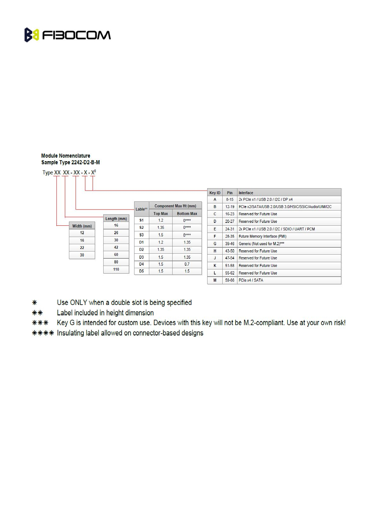
About the naming rules of M.2, L831-EA adopts the Type 3042-S3-B (30mmx42mm,the maximum
thickness of element layer of Top surface is 1.5mm, the thickness of PCB is 0.8mm, Key ID is B).
L831-EA Module Hardware User Manual Page
18
of
43
3.3 M.2 Connector
Recommend to use the M.2 connector from LOTES, the type is APCI0026-P001A,the package of
connector design please refer to the relevant specifications.
As shown in Figure 3-2:
Figure 3-2 Size of APCI0026-P001A M.2 connector
L831-EA Module Hardware User Manual Page
19
of
43
4 Hardware Overview
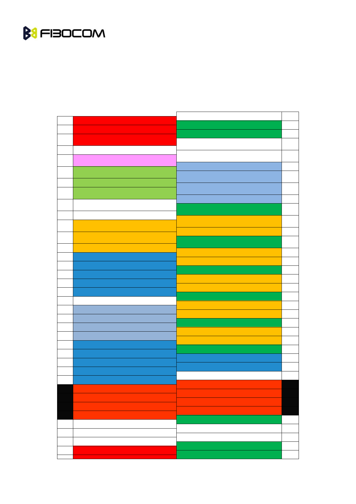
4.1 Pins Definition
4.1.1 Pins Number
CONFIG_2
75
74
+3.3V
GND
73
72
+3.3V
GND
71
70
+3.3V
CONFIG_1
69
68
CLK32K
RESET#
67
66
SIM_DETECT
ANTCTL3
65
64
NC
ANTCTL2
63
62
NC
ANTCTL1
61
60
NC
ANTCTL0
59
58
NC
GND
57
56
NC
NC
55
54
NC
NC
53
52
NC
GND
51
50
NC
NC
49
48
TX_BLANKING
NC
47
46
SYSCLK
GND
45
44
GNSS_IRQ
NC
43
42
GNSS_SDA
NC
41
40
GNSS_SCL
GND
39
38
NC
SSIC-TXP/USB3.0-TX+(NC)
37
36
UIM_PWR
SSIC-TXN/USB3.0-TX-(NC)
35
34
UIM_DATA
GND
33
32
UIM_CLK
SSIC-RXP/USB3.0-RX+(NC)
31
30
UIM_RESET
SSIC-RXN/USB3.0-RX-(NC)
29
28
I2S_WA
GND
27
26
W_DISABLE2#
DPR
25
24
I2S_RX
WOWWAN#
23
22
I2S_TX
CONFIG_0
21
20
I2S_CLK
Notch
Notch
Notch
Notch
Notch
Notch
Notch
Notch
GND
11
10
LED1#(3.3V)
USB D-
9
8
W_DISABLE1#(3.3V)
USB D+
7
6
FUL_CARD_POWER_OFF#(1.8V)
GND
5
4
+3.3V
GND
3
2
+3.3V
L831-EA Module Hardware User Manual Page
20
of
43
CONFIG_3
1
Figure4- 2 Pins Definition (Top View)
4.1.2 Pins Description
The description of L831-EA pins as listed below:
Pin#
Name
I/O
Reset
Value
Idle
Value
Description
1
CONFIG_3
O
L
L
The internal connects with GND, the
interface type of L831-EA module is
WWAN-SSIC0.
2
+3.3V
PI
The main power input, the voltage
range is: 3.135V ~ 4.4V
3
GND
GND
4
+3.3V
PI
The main power input, the voltage
range is: 3.135V ~ 4.4V
5
GND
GND
6
FUL_CARD_POWER_OFF#
I
PU
PU
Off control signal,the internal 200K
ohm will be pulled down, CMOS 1.8V
7
USB D+
I/O
USB 2.0 signal+
8
W_DISABLE1#
I
PU
PU
WWAN Disable, Low active, CMOS
3.3V
9
USB D-
I/O
USB 2.0 signal-
10
LED1#
O
OD
OD
System status LED,drain output, low
level is available, CMOS 3.3V
11
GND
GND
12
Notch
Notch
13
Notch
Notch
14
Notch
Notch
15
Notch
Notch
16
Notch
Notch
17
Notch
Notch
18
Notch
Notch
19
Notch
Notch
20
I2S_CLK
O
T
T
I2S serial clock,CMOS 1.8V
21
CONFIG_0
O
NC
NC
NC,the interface type of L831-EA
L831-EA Module Hardware User Manual Page
21
of
43
module is WWAN-SSIC0
22
I2S_RX
O
T
T
I2Sserial data output, CMOS 1.8V
23
WOWWAN#
O
PU
PU
The module wake up the Host device
signal,low level is available,CMOS
1.8V.
24
I2S_TX
I
T
T
I2Sserial data input, CMOS 1.8V
25
DPR
I
Body SAR Detect,CMOS 1.8V
26
W_DISABLE2#
I
PU
PU
GPS Disable signal, low level is
available, CMOS 1.8V (not support
yet).
27
GND
GND
28
I2S_WA
O
T
T
I2S left/right channel clock signal,
CMOS 1.8V
29
SSIC-RXN/USB3.0-RX-(NC)
NC
30
UIM_RESET
O
PP
PP
Reset signal of USIM card.
31
SSIC-RXP/USB3.0-RX+(NC)
I/O
NC
32
UIM_CLK
O
PP
PP
Clock signal of USIM card.
33
GND
GND
34
UIM_DATA
I/O
PU
PU
Data signal of USIM card. the
internal 4.7K resistance will be pulled
up.
35
SSIC-TXN/USB3.0-TX-(NC)
NC
36
UIM_PWR
O
Power output of SIM card, 1.8V/3.0V
37
SSIC-TXP/USB3.0-TX+(NC)
NC
38
NC
NC
39
GND
GND
40
GNSS_SCL
O
PU
PU
I2C serial data signal clock, the
internal 4.7K resistance will be pulled
up, CMOS 1.8V.
41
NC
NC
42
GNSS_SDA
I/O
PU
PU
I2C serial data signal data, the
internal 4.7K resistance will be pulled
up, CMOS 1.8V
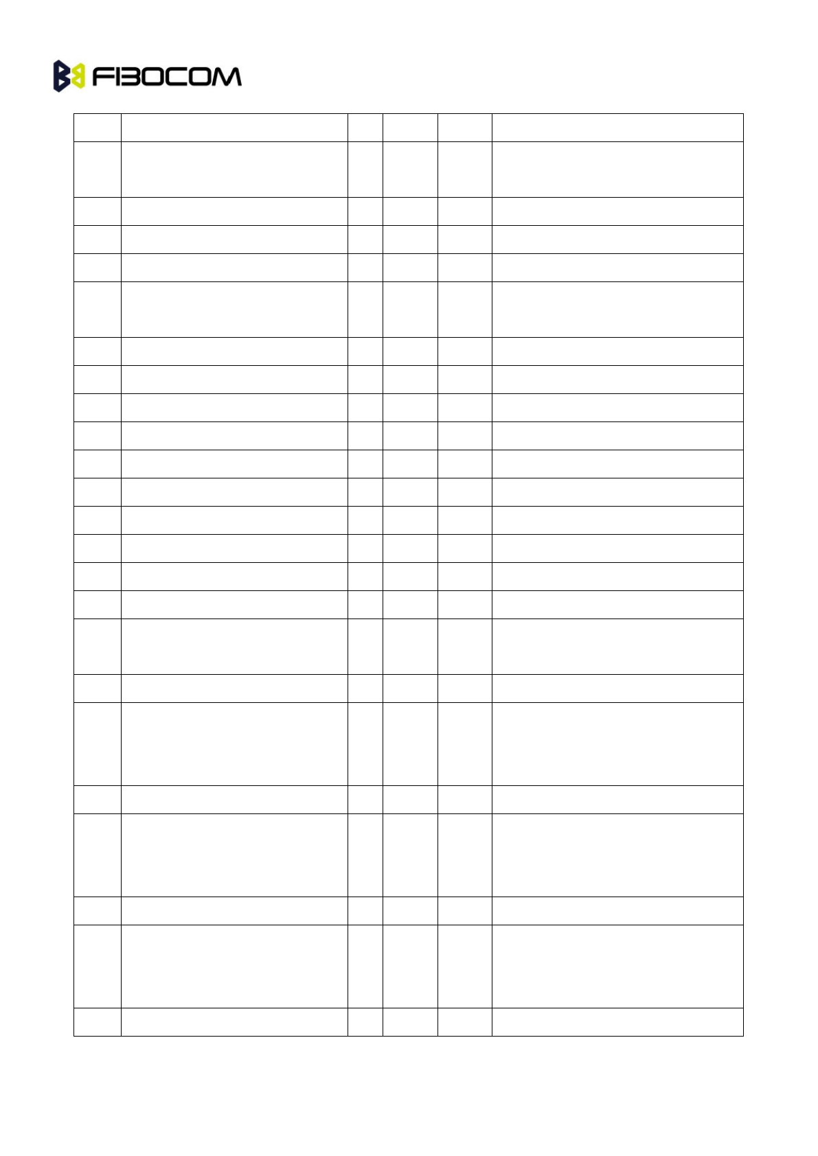
L831-EA Module Hardware User Manual Page
22
of
43
43
NC
NC
44
GNSS_IRQ
I
PU
PU
The switch interrupt signal of
Win8/Android system.
45
GND
GND
46
SYSCLK
O
L
L
26MHz clock output.
47
NC
NC
48
TX_BLANKING
O
L
L
GSM TDMA Timer output signal, the
GPS control signal, CMOS 1.8V
49
NC
NC
50
NC
NC
51
GND
GND
52
NC
NC
53
NC
NC
54
NC
NC
55
NC
NC
56
NC
NC
57
GND
GND
58
NC
NC
59
ANTCTL0
O
Tunable antenna control signal
GPO,CMOS 1.8V (not support yet)
60
NC
NC
61
ANTCTL1
O
L
L
Tunable antenna control signal, MIPI
RFFE SDATA, CMOS 1.8V (not
support yet)
62
NC
NC
63
ANTCTL2
O
L
L
Tunable antenna control signal, MIPI
RFFE SCLK, CMOS 1.8V (not
support yet)
64
NC
NC
65
ANTCTL3
O
Tunable antenna control signal, MIPI
RFFE VIO, CMOS 1.8V (not support
yet)
66
SIM_DETECT
I
PU
PU
SIM Detect,CMOS 1.8V,390K ohm
L831-EA Module Hardware User Manual Page
23
of
43
will be pulled up.
67
RESET#
I
PU
PU
External reset signal input, CMOS
1.8V
68
CLK32K
O
32KHz clock output.
69
CONFIG_1
O
L
L
The internal connects with GND, the
interface type of L831-EA module is
WWAN-SSIC0.
70
+3.3V
PI
The main power input, the voltage
range is : 3.135V ~ 4.4V
71
GND
GND
72
+3.3V
PI
The main power input, the voltage
range is : 3.135V ~ 4.4V
73
GND
GND
74
+3.3V
PI
The main power input, the voltage
range is : 3.135V ~ 4.4V
75
CONFIG_2
O
L
L
The internal connects with GND, the
interface type of L831-EA module is
WWAN-SSIC0.
Note :put the pins not used in circuit design NC directly.
PI:Power Input
H:High Voltage Level
L:Low Voltage Level
PD:Pull-Down
PU:Pull-Up
T:Tristate
OD:Open Drain
PP:Push-Pull
L831-EA Module Hardware User Manual Page
24
of
43
5 Hardware Interface
5.1 Power Interface
5.1.1 Power Supply
L831-EA module requires a 3.135V~ 4.4V DC power supply to provide the maximum GSM emission
current with 2A.
Input power supply requirements as listed below:
Parameters
Minimum
Recommended
Maximum
Unit
+3.3V
3.135
3.3
4.4
V
Note:
1. The ripple of Power supply must be lower than 200mV.
2. The minimum value of power supply voltage drops shall more than 3.135V.
The filter capacitor design of the supply circuit is as follows:
Recommended
capacitor
Application
Description
330uF
Supply capacitor
Reduce power wave in call. The
value of capacitor is bigger better.
1uF,100nF
Digital signal noise
Filtering interference from clock and
digital signal.
39pF,33pF
700/850/900 MHz band
Filtering the RF reference.
18pF,8.2pF,6.8pF
1700/1800/1900,2100,2500/2600MHz band
Filtering the RF reference.
5.1.2 VSD2_1V8
VSD2_1V8 is the digital part circle`s` power supply within the module, VSD2_1V8 can use for the index
signal and the reference level. With the circle design only use for external low current application
(<50mA), and floating it if not use.
Parameters
Minimum
Recommended
Maximum
Unit
VSD2_1V8
1.7135
1.8
1.8865
V
VIH
0.7* VSD2_1V8
1.8
1.8865
V
VIL
-0.3
0
0.3* VSD2_1V8
V
L831-EA Module Hardware User Manual Page
25
of
43
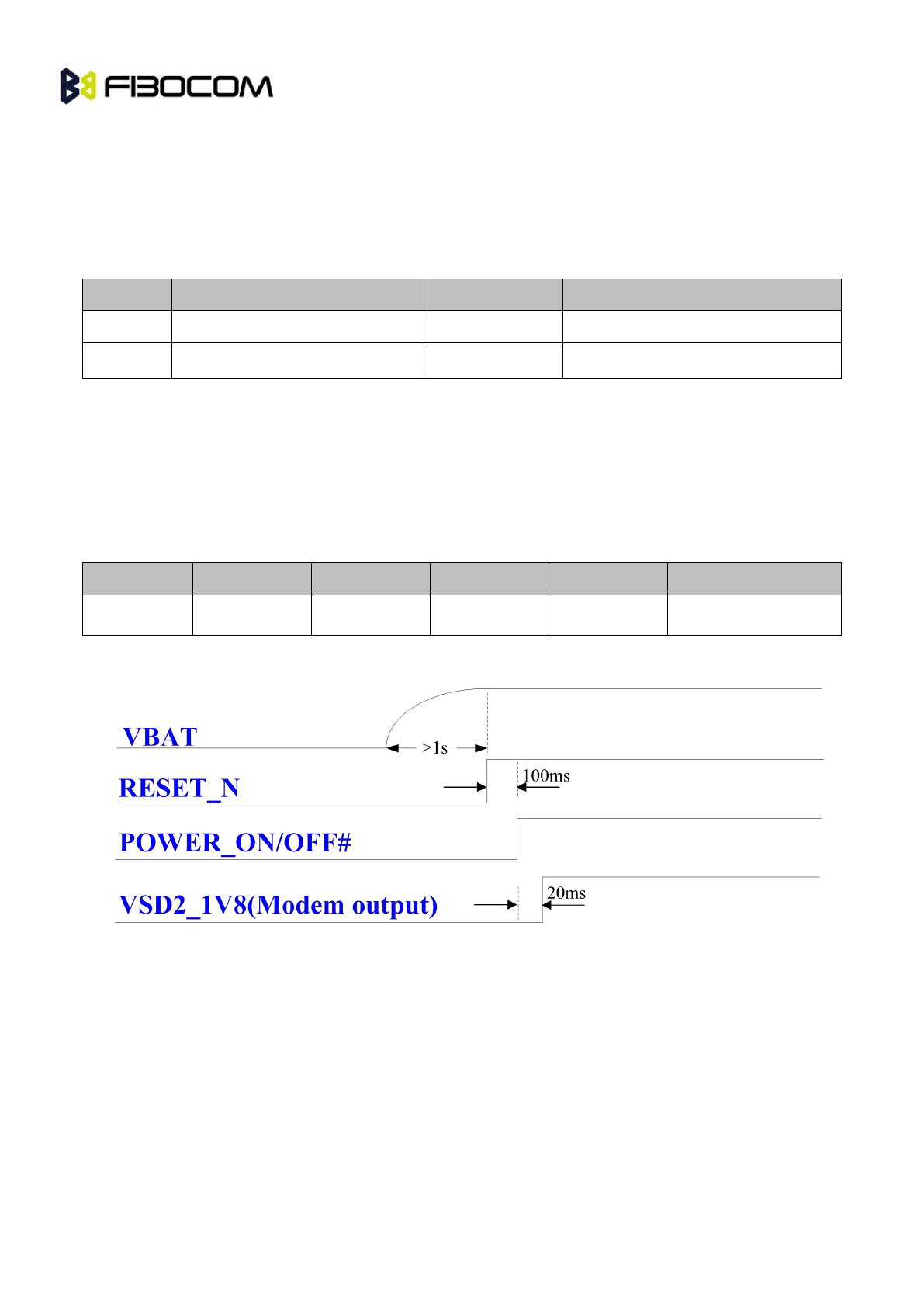
5.2 Power on/off and Reset Signal
L831-EA wireless module supports 2 control signals for the modules` power on/off and the reset
operation.
The definition of the pins as listed below:
Pin#
Pin Name
Electrical Level
Description
6
FUL_CARD_POWER_OFF#
CMOS 1.8V
Power on/off signal
67
RESET#
CMOS 1.8V
External reset signal input.
5.2.1 Power on/off Signal
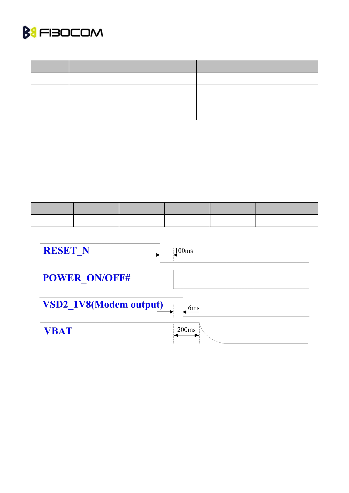
5.2.1.1 Power on
Clients can pull up the FUL_CARD_POWER_OFF# signal while the module is power on, then the module
will turn on.
The Pulse Timing requirements as listed below:
Parameters
Condition
Minimum
Typical
Maximum
Unit
Pulse Width
Power on
20
100
ms
The Figure5- 1 shows the power_on timing control:
Figure5- 1 Power_on Timing Control
5.2.1.2 Power off
L831-EA module supports two powers off modes. Through the software modes to turn off the module in
general condition. If the system halted or happen exceptions, use the following hardware modes to turn
L831-EA Module Hardware User Manual Page
26
of
43
off it, pull down the FUL_CARD_POWER_OFF# or floating. For details as listed below:
Off modes
Methods
Condition
Software
Send AT+CPWROFF commands.
Normal power_off
Hardware
Pull down the FUL_CARD_POWER_OFF#
or floating.
Only used for system halted or happens
exceptions and the software modes can
not be used.
The description of hardware power_off as follows ( Pull down the FUL_CARD_POWER_OFF# or
floating ):
While pulling down the FUL_CARD_POWER_OFF# signals or floating, the modules` PMU (Power
Management Unit) will be reset, then the module will get into off modes from working modes.
Note ①: the RESET_N signal must be pulled down before pulling down the FUL_CARD_POWER_OFF#
signal, and then the module will be turned off safely.
The Pulse Timing requirements as listed below:
Parameters
Condition
Minimum
Typical
Maximum
Unit
Pulse Width
Power off
5
100
ms
The Figure 5- 2 shows the power off timing control:
Figure5- 2 Power off Timing Control
5.2.1.3 Recommended Circuit Design of Power on/off signals
The recommended design of FUL_CARD_POWER_OFF# signal as follows:
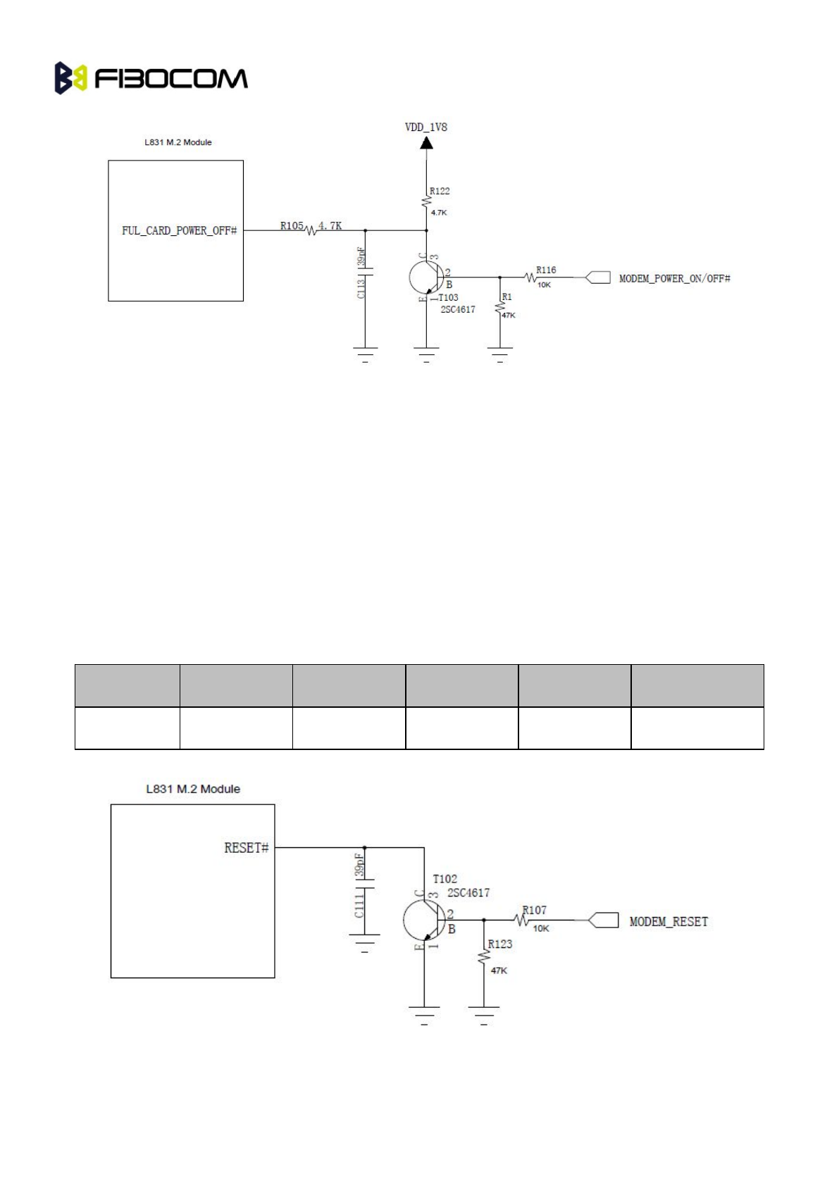
L831-EA Module Hardware User Manual Page
27
of
43
Figure 5- 3 the recommended design of FUL_CARD_POWER_OFF# signal
5.2.2 RESET Signal
L831-EA wireless module supports external reset function. The module can back to initial state through
Reset _N signal.
While the RESET# signal is active low and keep 100ms, the module will reset and restart. The internal
PMU cannot power cut while the clients execute the RESET function.
Note: Reset signal is sensitive signal line , while PCB layout, please keep it away from RF interference,
add the surrounding processing and recommend to decouple capacitor near the module. Don’t layout the
Reset signal in PCB edge or surface to avoid ESD causing system reset.
The requirements of Pulse Timing as listed below:
Parameters
Condition
Minimum
Typical
Maximum
Unit
Pulse Width
Reset
7
100
1000
ms
The recommended design as follows:
Figure5- 4 Recommended design of RESET# circuit
L831-EA Module Hardware User Manual Page
28
of
43
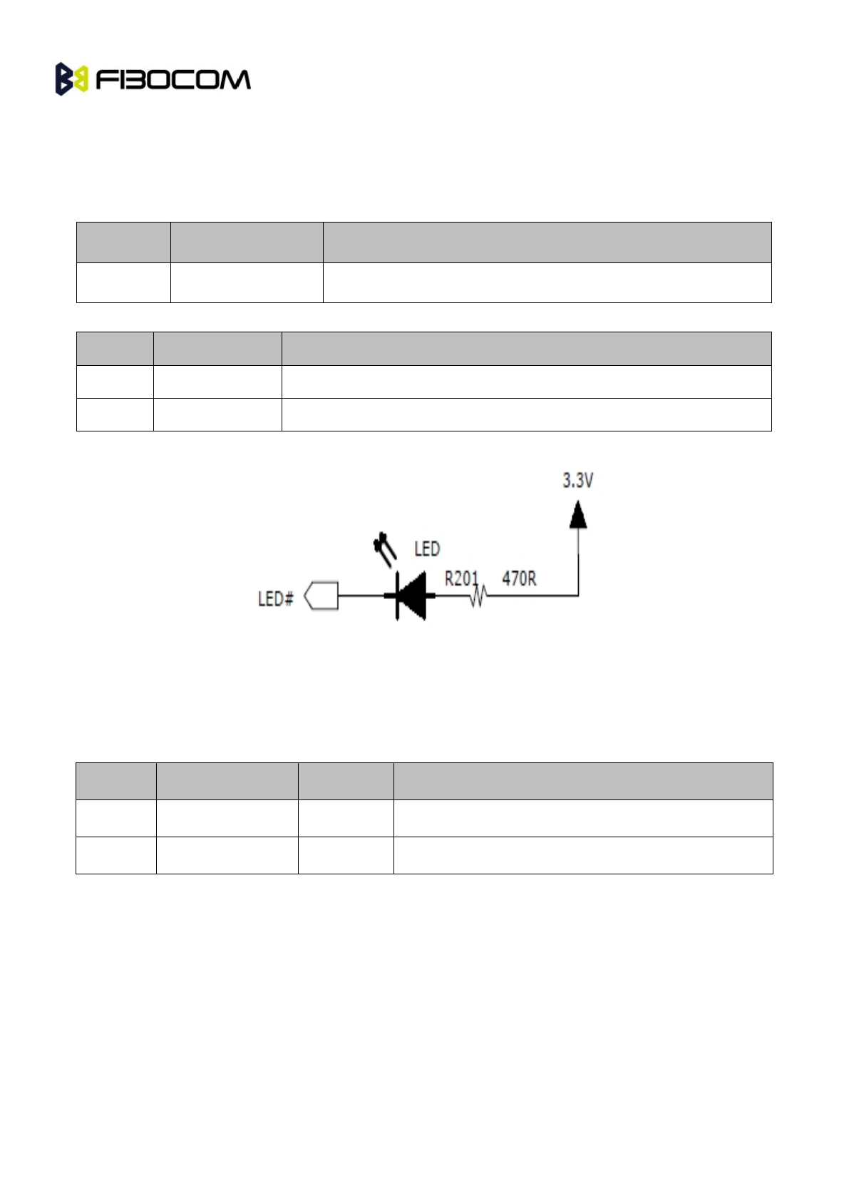
5.3 Index Signal
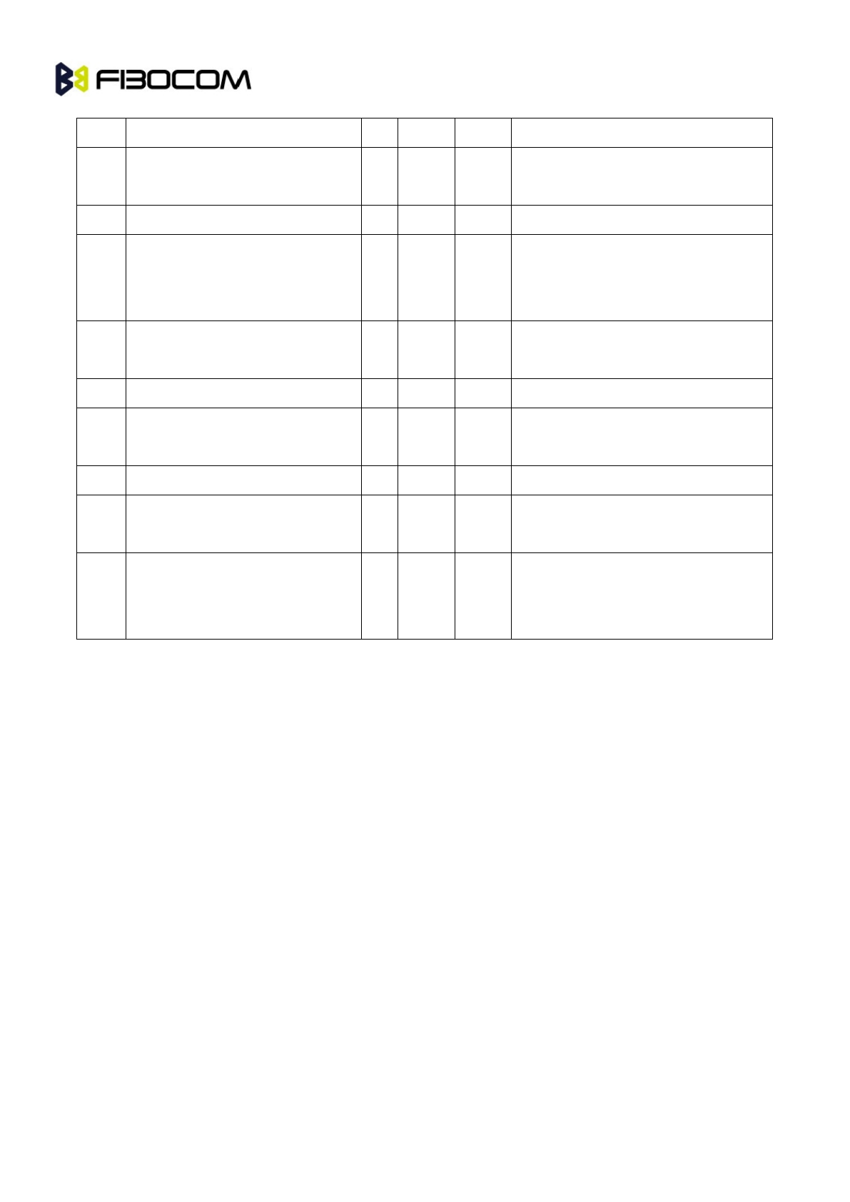
5.3.1 Index Signal Pins
L831-EA module used for providing drain output signal and indicate RF condition:
Pin #
Name
Description
10
LED1#
Close or open the condition indication of RF network, CMOS 3.3V
The condition description of LED1# signal as listed below :
No.
Condition
LED1#
1
RF open
Low level
2
RF closed
High level
The recommended design as follows:
Figure5- 5 Recommended design of LED condition index
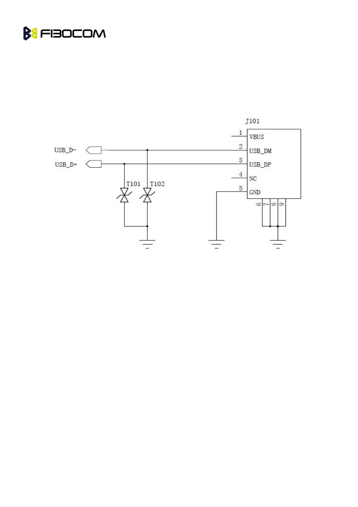
5.4 USB Interface
5.4.1 Definition of USB Interface
Pin No
Pin Name
I/O
Description
7
USB_DP
I/O
USB signal+
8
USB_DM
I/O
USB signal-
L831-EA wireless module supports USB 2.0. It should be installed USB driver before using on PC.
While L831-EA wireless module plugged into the PC, the USB interface with the drive can map 3 COM
ports and 4 NCM ports at PC end of Windows system, and for details as listed below:
Two COM ports for sending AT Commands.
One COM port for tracing LOG information.
Four NCM ports are VLAN ports, mainly used for initiating data services .
Note: The COM port can used as Modem COM port and initiate data services. But cause of the speed of
L831-EA Module Hardware User Manual Page
29
of
43
Modem COM port is so slow, and cannot up to 100Mbpss, the uplink requirements of LTE. So it is not
suggested. The Modem COM can be used to initiate data services temporarily only while the client`s NCM
port is useless.
5.4.2 Application for USB Interface
The recommended circuit design as follows:
Figure5- 6 Recommended circuit design of USB interface
T101 and T102 shall choose the TVS pipes witch less than 1pF.
VUSB supply power has connected within the module, so the VBUS pin of Host end can float.
USB_D+ and USB_D- is high speed differential signal line , the highest transmit speed is up to480Mbps.
Not the following requirements while PCB Layout:
USB_DP+ and USB_D- signal lines request with the same length, parallel, and try to avoid right
angle routing.
Around the USB_DP +and USB_D- signal lines should be packaged with GND.
Put the USB2.0 differential signal lines in the signal layer while are nearest to the ground.
USB signal lines shall far away from strong interference signals, like power supply.
Do the impedance matching, the impedance requests 90 ohm.
5.5 USIM Interface
L831-EA wireless module supports USIM and high speed SIM card, and does not supports 8-wire smart
USIM yet.
L831-EA Module Hardware User Manual Page
30
of
43
5.5.1 USIM Pins
Pin#
Name
Type
Description
36
UIM_PWR
O
USIM power supply signal
30
UIM_RESET
O
USIM Reset signal
32
UIM_CLK
O
USIM clock signal
34
UIM_DATA
I/O
USIM data signal
66
SIM_DETECT
I
The detection signal for SIM insetting
The default is 390K ohm resistance pulled up and
input.
High level: SIM is present.
Low level: SIM is absent
5.5.2 Description of USIM
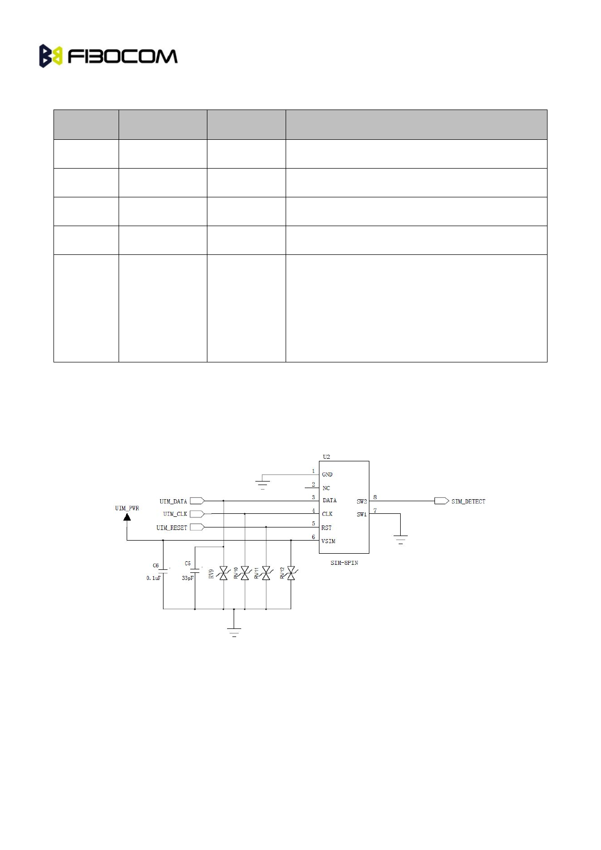
5.5.2.1 “Normally Closed”SIM Circuit Design
Referenced Circuit Design:
Figure5- 7 Reference Design of “Normally Closed” SIM Card Interface
Normally closed SIM Connector:
1)Pull out SIM card, pin 7 and pin 8 short-circuit .
2)Insert SIM card, pin 7 and pin 8 disconnect.
L831-EA Module Hardware User Manual Page
31
of
43
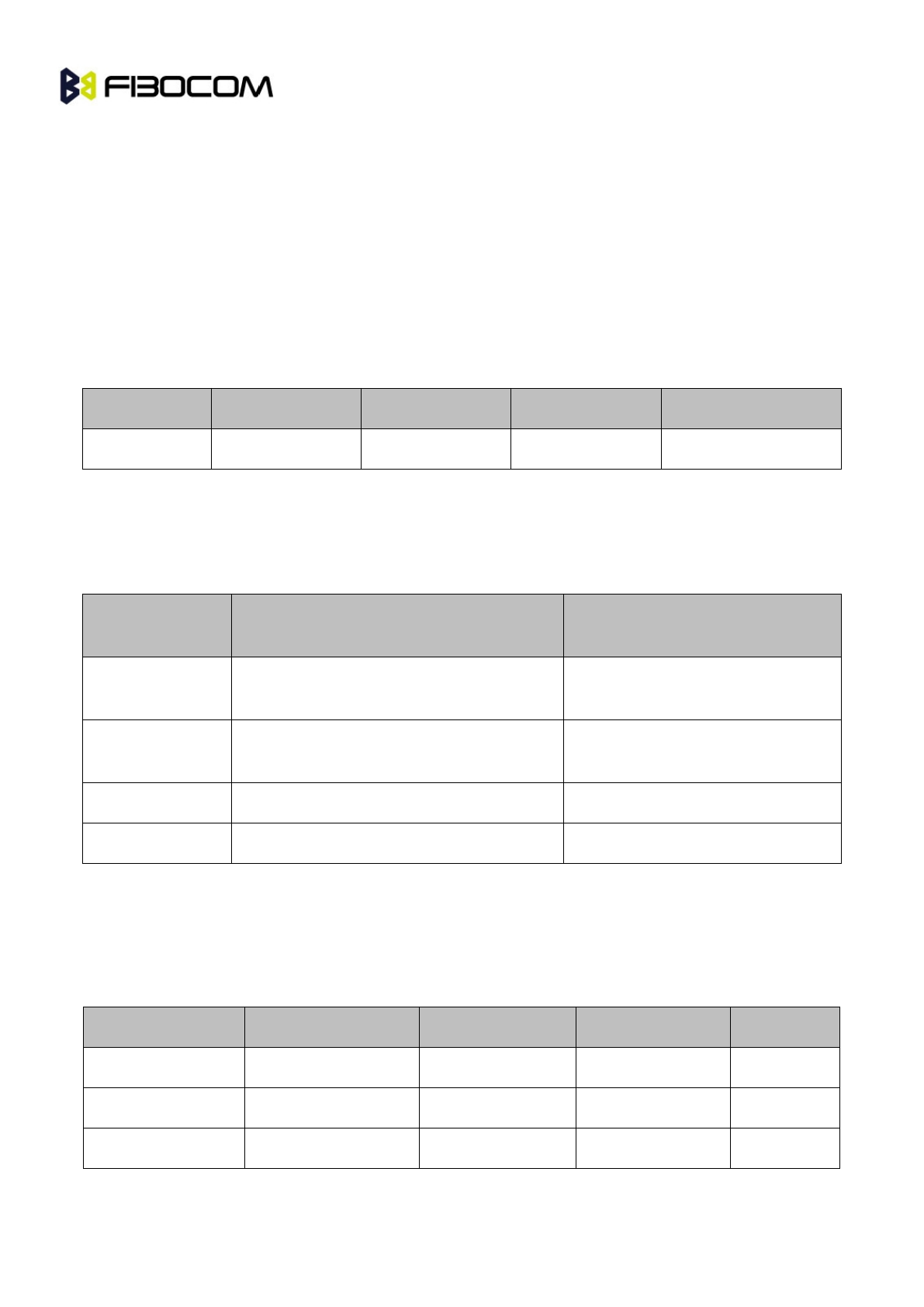
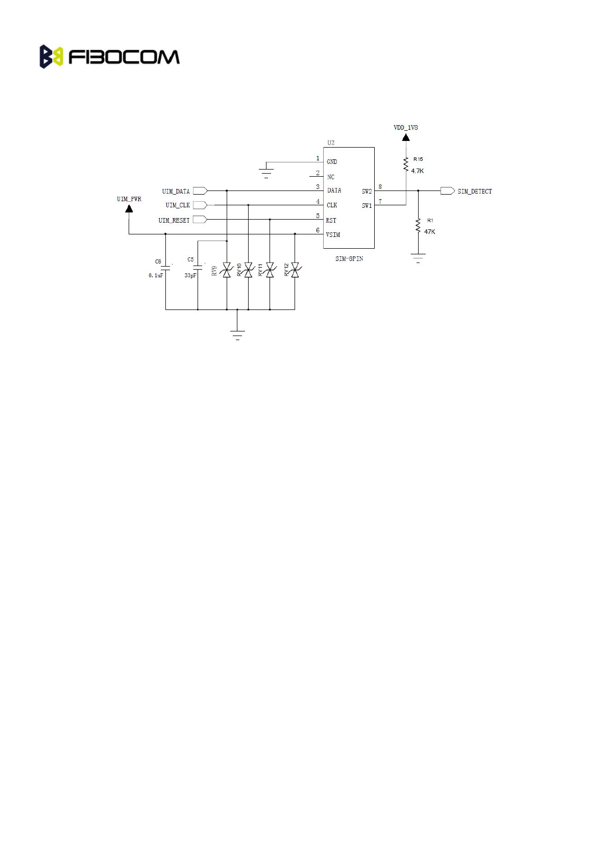
5.5.2.2 “Normally Open” SIM Circuit Design
Referenced Circuit Design:
Figure5- 8 “Reference Design of “Normally open” SIM Card Interface
Normally Open SIM Connector:
1)Pull out SIM card, pin 7 and pin 8 disconnect.
2)Inset SIM card, pin 7 and pin 8 short-circuit .
Note:
For improving EMC performance, SIM card connector should be closed to the module.
For improving the anti-jamming capability of SIM card, please choose the SIM card socket with
masking function.
Filtering capacitor on SIM card should be closed to SIM card pin.
SIM card signal need add ESD protection (just like TVS pipe), ESD components should be closed to
SIM card pin.
SIM_CD signal connection supports hot plug, default high level is available (switch to low level is
available through AT commands). If high level is detected, it means the SIM card is inserted.
5.5.3 USIM Design Points
The design of SIM interface is very important to its own normal working and the module.
There are several design guidelines that must be followed:
The layout and routing of SIM card should be away from EMI interference source , such as RF
antenna and digital switching signals.
To ensure signal integrity, the routing length between module and SIM card should not exceed
100mm.
To avoid mutual interference, the routing of UIM_CLK and UIM_DATA signal shall keep separate.

L831-EA Module Hardware User Manual Page
32
of
43
The signal lines of SIM cards shall do some ESD protection , and it request to choose the ESD
protected components with low capacitance, such as Zener diode. Recommend the clients to use the
ESD components and the equivalent capacitance shall be less than 33pF. ESD components shall
near to SIM card interfaces while layout.
5.5.4 USIM Hot Plug
L831-EA module supports the status detection function, and this function can realize hot plug of SIM
card .
5.5.4.1 Hardware Connection
The hot plug function of SIM card needs the cooperation of SIM_DETECT signal.
SIM_DETECT is low level while no SIM card; SIM_DETECT is high level while installing SIM card.
Principle description:
1)For “normally closed” SIM card, as shown in Figure 5-7.SIM_DETECT signal connects Pin8 (SW2) of
U2, pull down the Pin7 (SW1) to GND. SW2 and SW1 short-circuit while SIM card is not inserted, so
SW2 is low level. SW1 and SW2 disconnect while SIM card installed, SIM_DETECT is pulled high.
2)For “normally open“SIM card, as shown in Figure 5-8. SIM_DETECT signal connects Pin8 (SW2) of
U2 and pull down to ground through 47Kohm resistance. Pin 7 (SW1) shall be pulled up
with4.7Kohms. SW2 and SW1 is disconnected while SIM card is not inserted, so SW2 is low level.
SW1 and SW2 is short-circuiting while SIM card installed, SIM_DETECT is pulled high.
5.5.4.2 Software Configuration
“+MSMPD” is used for setting the state detection of SIM card.
AT+MSMPD=0, state detection function of SIM card is closed. The module does not detect the
SIM_DETECT signal.
AT+MSMPD=1, state detection function of SIM card is open. Detect the SIM card if installing or not
through the SIM_DETECT Pin .
SIM_DETECT is high level, SIM card is installed, and the module registers the network automatically.
SIM_DETECT is low level, SIM card is not inserted, and the module does not register the network.
Note: The parameters of “+MSMPD” is “1” by default. SIM_DETECT is the detection signal. While the
module first power on or plug after that, SIM_DETECT will detect if the SIM card is existing or not. Just
only if the SIM_DETECT is low level, the module will cannot read SIM card.
5.6 Digital Audio
L831-EA supports digital audio I2S interface.12S interface can support normal I2S modes and data
transmission of PCM modes. The level of I2S interface signal is 1.8V.
L831-EA Module Hardware User Manual Page
33
of
43
The description of I2S signal as listed below:
Pin#
Name
Type
Description
20
I2S2_CLK
O
Bit clock
28
I2S2_WA0
O
Left- right clock (LRCK)
22
I2S2_TX
O
Serial data output
24
I2S2_RX
I
Serial data input
5.6.1 Description of I2S Interface
L831-EA
Signal Direction
Audio CODEC I2S Port
I2S_CLK
I2S_CLK
I2S_WA
I2S_LRCK
I2S_RX
I2S_SDOUT
I2S_TX
I2S_SDIN
Note:
I2S interfaces can be configured to master or slave modes .
It supports various audio sample rates (48KHz, 44.1KHz, 32KHz, 24KHz, 22.5KHz, 16KHz, 12KHz,
11.025KHz, 8KHz).
5.6.2 Description of PCM Interface
L831-EA
Signal Direction
Audio CODEC PCM Port
I2S_CLK0(PCM_CLK,PCM clock signal)
PCM_CLK (PCM clock signal)
I2S_WA0(PCM_SYNC,PCM frame
synchronization signal)
PCM_SYNC (PCM frame
synchronization signal )
I2S_RX(PCM_DIN,PCM data input)
PCM_DOUT (PCM data output)
I2S_TX(PCM_DOUT,PCM data output)
PCM_DIN (PCM data input)
Description:
PCM interfaces can be configured to master or slave modes.
Supports short frame synchronization under16 bit, 32bit, 48bit and 64bit modes.
Supports sending data in burst modes and continuous modes.
Supports clock length of frame synchronization signal and rising edge/ falling edge trigger
L831-EA Module Hardware User Manual Page
34
of
43
configuration of data transmission.
Supports various audio sample rates (48KHz,44.1KHz,32KHz, 24KHz,22.5KHz,16KHz,12KHz,8KHz,
11.025KHz).
Note: Cause the timing of I2S modes is easier than PCM modes and easier to fit, recommend clients to
use transmission audio of I2S mode. While transmission with PCM modes, the PCM timing sequence is
difficult to fit to make the tone quality become bad.
5.7 Android/Win8Dual System Switch Control Interface
L831-EA module supports Win8/Android dual system switch, check and achieve the dual system switch
through interrupt signal ”GNSS_IRQ”.
Pin#
Name
I/O
Description
44
GNSS_IRQ
I
Win8/Android dual system switch detection signal,
CMOS 1.8V
The function definition of GNSS_IRQ signal as listed below:
No.
GNSS_IRQ
Function
1
High/Floating
Support Win8 system, the module`s USB ports shall set as MBIM modes.
2
Low
Support Android system, the module`s `USB ports shall set as
3ACM modes.
Description:
1. Check and achieve the Win8/Android system switch through GNSS_IRQ level when the module
power on. Keep the GNSS_IRQ level stability during booting.
2. Check and achieve the Win8/Android system switch through GNSS_IRQ rising edge/ falling edge
while the module power on, the de-bouncing time sets as 100ms. The module will reboot after
meeting the requirements and can switch different system supports.
5.8 W_DISABLE# Interface
5.8.1 Description of WWAN_DISABLE# Interface
L831-EA module provides through hardware to open/close the WWAN RF function signal, this function
can also controlled by AT commands.
Pin#
Name
I/O
Description
8
W_DISABLE1#
I
WWAN open/close signal ,CMOS 3.3V
The definition of W_DISABLE# signal as listed below:
L831-EA Module Hardware User Manual Page
35
of
43
5.8.2 Description of GPS_DISABLE# Interface
L831-EA module provides through hardware to open/close GPS function signal, this function can also
control by AT commands.
Pin#
Name
I/O
Description
26
W_DISABLE
2#
I
GPS open/close signal , and the
signal with 1.8V
The definition of GPS_DISABLE# signal as listed below:
No.
GPS_DISABLE#
Description
1
Low
GPS closed
2
High
GPS open
3
Floating
The function of GPS defined by AT commands, keeps open by default.
Note: this function don`t support yet.
5.9 TX_BLANKING Interface
Output low level by default, the TX_BLANKING output the pulse signal that synchronized with GSM burst
timing while the module works in GSM band. Cause GSM transmitting may interfere the receiving of GPS
signal, close GPS or stop the data receiving of GPS while AP detected TX_BLANKING pulse signal.
Pin#
Name
I/O
Description
48
TX_BLANKING
O
External GPS control signal
5.10 The WAKEUP_HOST Interface
The module supports the WAKEUP_HOST function, the pin is high level by default, but it outputs low level
while awaking Host.
Pin#
Name
I/O
Description
23
WOWWAN#
O
The module wakes up Host signal with 1.8V,and low
level is available.
No.
W_DISABLE#
Function
1
Low
WWAN closed
2
High
WWAN opened
3
Floating
The function of WWAN defined by AT commands , and keep open by
default .
L831-EA Module Hardware User Manual Page
36
of
43
5.11 BODY_SAR Interface
L831-EA module supports BODY_SAR (DPR pin) function.
BODY_SAR is input signal (the signal is output directly by the AP end), with high level by default, and low
level is effectively. While the human nearing, AP can detect it through the distance sensor, then output the
BODY_SAR signal with low level. While the module detected the signal through the interruption, the
module `s Tx power will be reduced and the threshold value can be set by the AT commands.
Pin#
Name
I/O
Description
25
DPR
I
BODY_SAR detection
5.12 Description of I2C Interface
L831-EA module supports one 12C interface, default configuration is I2C master. The I2C can used for
driving external 12C slave device, such as Audio codes and so on.
Pin#
Name
I/O
Description
42
GNSS_SDA
I/O
I2C control signal input/output ,1.8V signal
40
GNSS_SCL
O
I2C control clock signal, 1.8V signal
The signal connection between L831-EA module and external 12C slave device ( such as Audio Codec)
as listed below:
L831-EA
Direction
Audio Codec I2C Port
GNSS_SDA
I2C_SDA
GNSS_SCL
I2C_SCL
5.13 Clock Interface
L831-EA module supports one 26MHz clock output and one 32KHz clock output.
Pin#
Name
I/O
Description
68
CLK32K
O
32K clock output ,
46
SYSCLK
O
26Mclock output , (recommend used for external GPS, and can
also used as audio codec`s MCLK)
5.14 Config Interface
L831-EA module provides four config pins and with the configuration of WWAN-USB3.0-0.
PIN#
Name
I/O
Description
Value
L831-EA Module Hardware User Manual Page
37
of
43
1
CONFIG_3
O
Connect to GND within the module
0
21
CONFIG_0
O
NC
-
69
CONFIG_1
O
Connect to GND within the module
0
75
CONFIG_2
O
Connect to GND within the module
0
The configuration of M.2 Socket 2 Module as listed below :
Config_0
(pin21)
Config_1
(pin69)
Config_2
(pin75)
Config_3
(pin1)
Module Type and Main
Host Interface
Port Configuration
GND
GND
GND
GND
SSD-SATA
N/A
GND
GND
N/C
GND
WWAN-PCIe
N/A
GND
GND
GND
N/C
WWAN-USB3.0
0
5.15 RF Interface
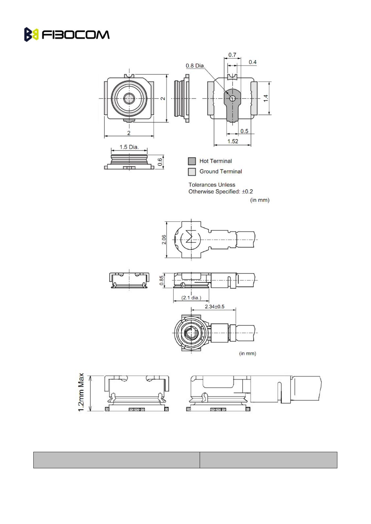
5.15.1Description of RF Connector
L831-EA module provides two RF connector for the connection of external antenna , the MAIN means the
main antenna of RF, and DIV means the diversity antenna .
Figure 5-9 RF connectors Diagram
5.15.2Description of RF Connecting Seat
L831-EA module adopts the RF connecting seat with Murata MM4829-2702, the size is 2*2*0.6mm, and
the structure diagram as follows:
L831-EA Module Hardware User Manual Page
38
of
43
Figure 5-10 Structure diagram of RF connecting seat
Figure 5-11 0.81mm coaxial line
Figure 5-12 RF connector insert into RF connecting seat
5.15.3Main Performance of RF Connector
Rated conditions
Environment condition

L831-EA Module Hardware User Manual Page
39
of
43
Frequency range
DC to 6GHz
Temperature range :
Characteristic impedance
50Ω
–40°C to +85°C
5.16 Other Interfaces
The following interfaces are not supported now: GPIO and Tunable ANT.
L831-EA Module Hardware User Manual Page
40
of
43
6 Electrical and Environmental
6.1 Electrical
This table shows the electrical features range of L831-EA module.
Parameter
Minimum Value
Maximum Value
Unit
Power supply
0
4.4
V
Digital Signal
0
1.9
V
6.2 Environmental
This table shows the environmental features of L831-EA module
Parameter
Minimum Value
Maximum Value
Unit
Operational Temperature
-30
+55
°C
Storage Temperature
-40
+85
°C
L831-EA Module Hardware User Manual Page
41
of
43
7 RF Interface
7.1 Operating Band
7.1.1 Antenna Band
Operating
Band
Description
Mode
Tx (MHz)
Rx (MHz)
Band 1
IMT 2100MHz
LTE FDD/WCDMA
1920 - 1980
2110 - 2170
Band 2
PCS 1900MHz
LTE FDD/WCDMA/GSM
1850 - 1910
1930 - 1990
Band 3
DCS 1800MHz
LTE FDD/GSM
1710 - 1785
1805 - 1880
Band 4
AWS 1700MHz
LTE FDD
1710 - 1755
2110 - 2155
Band 5
CLR 850MHz
LTE FDD/WCDMA/GSM
824 - 849
869 - 894
Band 7
IMT-E 2600Mhz
LTE FDD
2500 - 2570
2620 - 2690
Band 8
E-GSM 900MHz
LTE FDD/WCDMA/GSM
880 - 915
925 - 960
Band 13
US 700MHz blocks C
LTE FDD
777 - 787
746 - 756
Band 17
US 700MHz blocks B/C
LTE FDD
704 - 716
734 - 746
Band 18
Japan 850MHz
LTE FDD
815 – 830
860 – 875
Band 19
Japan Extend 850MHz
LTE FDD
830 – 845
875 – 890
Band 20
EUDD 800MHz
LTE FDD
832 - 862
791 - 821
7.2 RF PCB Design
7.2.1 Routing Principle
L831-EA module adopts double RF antennas, the MAIN_ANT used for transmitting and receiving, the
DIV_ANT used for receiving. On the one hand, diversity antenna can improve the receiving sensitivity; on
the other hand, it can also improve the download speed. Because the L831-EA module belong to LTE
module, the Antenna need double antennas can meet the performance requirements.

L831-EA Module Hardware User Manual Page
42
of
43
7.2.2 Impedance Design
The impedance of RF signal lines should be controlled within 50ohm.
7.3 Antenna Design
7.3.1 Antenna Design Requirements
(1) Antenna Efficiency
Antenna efficiency is the ratio of antenna input power to radiation power. Cause the return loss, material
loss, and coupling loss, the radiation power is always lower than the input power.
Recommended value> 40% (–4dB)
(2) S11 or VSWR
S11 can indicates the 50ohm`s matched-degree of antenna .To some degree, it affects the antenna
efficiency. It can measure the indicator through VSWR test, recommended value: S11 < –10 dB.
(3) Polarization
The antenna`s polarization means the rotate direction of electric field in the direction of the maximum
radiation.
Recommend to use linear polarization: it would be better if the polarization direction of diversity antenna is
different from main antenna.
(4) Radiation Pattern
Radiation pattern is the antenna`s electromagnetic-field strength in all directions of far field .Half-wave
dipole antenna is the most suitable terminal antenna.
If it is built-in antenna, PIFA antenna is recommended:
Antenna area (H x W x L): 6mm x 10mm x 100mm. PIFA or IFA antenna is recommended.
Radiation Pattern: Omni-directional.
(5) Gain and Direction
The direction of the antenna is the electromagnetic field strength of the electromagnetic wave in all
directions. The gain is a collection of antenna efficiency and the direction of antenna.
Recommended antenna gain≤ 3dBi
(6) Interference
Besides the antenna`s performance, the other interference on the PCB board can also affect the
module`s performance. To ensure the module`s high performance, we must have a good control to the
interference.
Suggestions: such as the routing of Speak, LCD, CPU and FPC, the audio circuits and the power part
shall try to keep away from the antenna. At the same time, note the corresponding isolation and shielding,

L831-EA Module Hardware User Manual Page
43
of
43
or do some filtering on the routing.
(7)TRP/TIS
TRP (Total Radiated Power):
GSM850/900>28dBm
GSM DCS1800/PCS1900 >25dBm
WCDMA Band 1,2,4,5,8>19dBm
LTE FDD Band 1,2,3,5,7,8,13,17,18,19,20 >19dBm
TIS (Total Isotropic Sensitivity):
GSM850,GSM 900,DCS1800,PCS1900 <-102dBm
WCDMA Band1,2,4,5,8<-102dBm
LTE FDD Band1,2,3,5,7,8,13,17,18,19,20 <-95dBm (10MHz band width)