Fibocom Wireless M910GL LTE(CatM1, NB-IoT) Module User Manual
Fibocom Wireless Inc. LTE(CatM1, NB-IoT) Module Users Manual
Users Manual

Reproduction forbidden without Fibocom Wireless Inc. written authorization - All Rights Reserved.
M910-GL Hardware User Manual Page 1 of 45
M910-GL Series Hardware User Manual
Version: V1.0.1
Update date: Mar 21, 2018
Reproduction forbidden without Fibocom Wireless Inc. written authorization - All Rights Reserved.
M910-GL Hardware User Manual Page 2 of 45
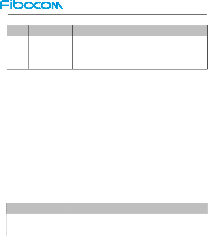
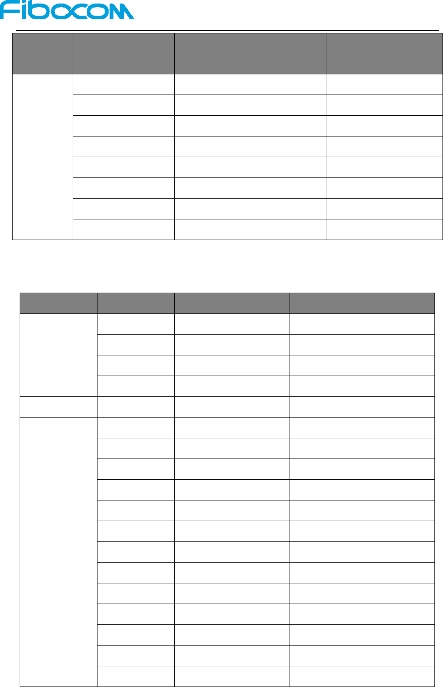
Applicability Table
No.
Product model
Description
1
M910-GL-00-00
MCP is 1G + 512M and supports MAIN_ANT and GNSS_ANT
Copyright
Copyright©2017 Fibocom Wireless Co., Ltd. All rights reserved.
Without the prior written permission of the copyright holder, any company or individual is
prohibited to excerpt, copy any part of or the entire document, or distribute the document in any
form.
Notice
The document is subject to update from time to time owing to the product version upgrade or
other reasons. Unless otherwise specified, the document only serves as the user guide. All the
statements, information and suggestions contained in the document do not constitute any explicit
or implicit guarantee.
Version Record
Version
Update Date
Description
V1.0.0
2017-12-24
Initial version
V1.0.1
2018-03-21
Add VBUS feature description

Reproduction forbidden without Fibocom Wireless Inc. written authorization - All Rights Reserved.
M910-GL Hardware User Manual Page 3 of 45
Contents
1 Foreword ................................................................................................... 5
1.1 Introduction ............................................................................................ 5
1.2 Safety Instruction .................................................................................... 5
1.3 Reference Standards ................................................................................ 6
1.4 Related Document ................................................................................... 6
1.5 EU Declaration of Conformity (DoC) ........................................................ 7
1.6 Federal Communication Commission Interference Statement ........................ 8
1.7 IC Statement ......................................................................................... 10
2 Product Overview ..................................................................................... 12
2.1 Product Introduction .............................................................................. 12
2.2 Product Specifications ............................................................................ 12
2.3 Hardware Diagram ................................................................................ 13
3 Application Interface ................................................................................ 15
3.1 LGA Interface ....................................................................................... 15
3.1.1 Pin Distribution ...................................................................................... 15
3.1.2 Pin definition .......................................................................................... 16
3.2 Power Supply ........................................................................................ 20
3.2.1 Power Supply .......................................................................................... 20
3.2.2 1.8V Output ............................................................................................ 20
3.2.3 Power consumption ................................................................................. 20
3.3 Control Signal ....................................................................................... 22
3.3.1 Module start-up....................................................................................... 23
3.3.2 Module shutdown .................................................................................... 24
3.3.3 Module reset ........................................................................................... 25
3.4 USB Interface ....................................................................................... 26
3.4.1 USB interface definition ........................................................................... 26
3.5 USIM Interface ..................................................................................... 27
3.5.1 USIM pin ................................................................................................ 27
3.5.2 USIM interface circuit ............................................................................. 27
3.5.3 USIM design requirements ....................................................................... 29
3.6 UART Interface ..................................................................................... 29
3.6.1 UART interface definition ........................................................................ 29
3.6.2 UART interface application ...................................................................... 30

Reproduction forbidden without Fibocom Wireless Inc. written authorization - All Rights Reserved.
M910-GL Hardware User Manual Page 4 of 45
3.7 Status Indicator ..................................................................................... 30
3.8 PCM/IIS ............................................................................................... 31
3.8.1 Digital voice interface definition .............................................................. 31
3.8.2 Interface description ................................................................................ 31
3.8.3 Signal description ................................................................................... 31
3.9 ADC function ....................................................................................... 31
4 Antenna Interface ..................................................................................... 32
4.1 Antenna design ..................................................................................... 32
4.1.1 Antenna RF connector ............................................................................. 32
4.1.2 RF output power of M910-GL .................................................................. 33
4.1.3 RF receiving sensitivity of M910-GL ......................................................... 34
4.1.4 Operating frequency of M910-GL supported bands (MHz) ......................... 35
4.2 Antenna Design ..................................................................................... 36
4.2.1 Antenna design requirements .................................................................... 36
5 Electrical Characteristics .......................................................................... 37
5.1 Limiting voltage range ........................................................................... 37
5.2 Environment temperature range ............................................................... 38
5.3 Electrical characteristics of the interface in operating status ........................ 38
5.4 Environmental reliability requirements ..................................................... 39
5.5 ESD characteristics ................................................................................ 40
6 Structure Specification.............................................................................. 41
6.1 Product Appearance ............................................................................... 41
6.2 Dimension of Structure .......................................................................... 42
6.3 SMT Patch ............................................................................................ 42
6.4 Storage ................................................................................................. 42
6.4.1 Storage life ............................................................................................. 42
6.4.2 Baking .................................................................................................... 43
6.5 Packaging ............................................................................................. 43
6.5.1 Tape packaging ....................................................................................... 44
6.5.2 Packaging list (TBD) ............................................................................... 44

Reproduction forbidden without Fibocom Wireless Inc. written authorization - All Rights Reserved.
M910-GL Hardware User Manual Page 5 of 45
1 Foreword
1.1 Introduction
This document describes the electrical characteristics, RF performance, structure size, application
environment, etc. of M910-GL module. With the assistance of the document and other instructions,
the developers can quickly understand the hardware functions of the M910-GL module and
develop products.
1.2 Safety Instruction
By following the safety guidelines below, you can protect the personal safety and help protect the
product and work environment from potential damage. Product manufacturers need to
communicate the following safety instructions to end users. In case of failure to comply with these
safety rules, Fibocom will not be responsible for the consequences caused by the user’s misuse.
Road safety first! When you drive, do not use the handheld devices even if it
has a hand-free feature. Please stop and call!
Please turn off the mobile device before boarding. The wireless feature of the
mobile device is not allowed on the aircraft to prevent interference with the
aircraft communication system. Ignoring this note may result in flight safety
issue or even breaking the law.
When in a hospital or health care facility, please be aware of restrictions on
the use of mobile devices. Radio frequency interference may cause medical
equipment to malfunction, so it may be necessary to turn off the mobile
device.
The mobile device does not guarantee that an effective connection can be
made under any circumstances, for example, when there is no prepayment for
the mobile device or the SIM is invalid. When you encounter the above
situation in an emergency, remember to use an emergency call, while keeping
your device turned on and in areas where signal is strong.
Your mobile device receives and transmits RF signals when it is powered on.

Reproduction forbidden without Fibocom Wireless Inc. written authorization - All Rights Reserved.
M910-GL Hardware User Manual Page 6 of 45
Radio interference occurs when it is near televisions, radios, computers, or
other electronic devices.
Keep the mobile device away from flammable gases. Turn off the mobile
device when near gas stations, oil depots, chemical plants or explosive
workplaces. There is a safety hazard in operating electronic equipment in any
potentially explosive environment.
1.3 Reference Standards
This design of the product complies with the following standards:
3GPP TS 51.010-1 V10.5.0: Mobile Station (MS) conformance specification; Part 1:
Conformance specification
3GPP TS 34.121-1 V10.8.0: User Equipment (UE) conformance specification; Radio
transmission and reception (FDD); Part 1: Conformance specification
3GPP TS 34.122 V10.1.0: Technical Specification Group Radio Access Network; Radio
transmission and reception (TDD)
3GPP TS 36.521-1 V10.6.0: User Equipment (UE) conformance specification; Radio
transmission and reception; Part 1: Conformance testing
3GPP TS 21.111 V10.0.0: USIM and IC card requirements
3GPP TS 51.011 V4.15.0: Specification of the Subscriber Identity Module -Mobile
Equipment (SIM-ME) interface
3GPP TS 31.102 V10.11.0: Characteristics of the Universal Subscriber Identity Module
(USIM) application
3GPP TS 31.11 V10.16.0: Universal Subscriber Identity Module (USIM) Application
Toolkit(USAT)
3GPP TS 36.124 V10.3.0: Electro Magnetic Compatibility (EMC) requirements for
mobile terminals and ancillary equipment
3GPP TS 27.007 V10.0.8: AT command set for User Equipment (UE)
3GPP TS 27.005 V10.0.1: Use of Data Terminal Equipment - Data Circuit terminating
Equipment (DTE - DCE) interface for Short Message Service (SMS) and Cell Broadcast
Service (CBS)
1.4 Related Document
FIBOCOM M910-GL LGA SMT Application Design Instruction
Reproduction forbidden without Fibocom Wireless Inc. written authorization - All Rights Reserved.
M910-GL Hardware User Manual Page 7 of 45
1.5 EU Declaration of Conformity (DoC)
Hereby we,
Name of manufacturer:
Fibocom Wireless Inc.
Address:
5/F,Tower A,Technology Building II,1057 Nanhai Avenue
Zip code & City:
Shenzhen
Country:
China
Telephone number:
+86 755 26525092
declare that this DoC is issued under our sole responsibility and that this product:
Product description:
LTE(CatM1, NB-IoT) Module
Type designation(s):
M910-GL
Trademark:
Fibocom
Batch / Serial number:
Object of the declaration (further identification of the radio equipment allowing
traceability; it may include a color image for the identification of the radio equipment):
is in conformity with the relevant Union harmonization legislation:
Radio Equipment directive: 2014 / 53 / EU
with reference to the following standards applied:
EN 301 489-1 V2.1.1; EN 301 489-19 V2.1.0;
EN 301 489-52 V1.1.0; EN 303 413 V1.1.1
EN 301 511 V12.5.1; EN 301 908-1 V11.1.1
EN 301 908-13 V11.1.2
EN 62311:2008
EN 60950-1:2006+ A11:2009 + A1:2010 + A12:2011 + A2:2013
The Notified Body SGS United Kingdom Limited, with Notified Body number 0890
performed:
Modules: B+C and issued the EU-type examination certificate.
Signed: Printed name: Yin Jixiong
Place and date of issue:2018-07-24
On behalf of Company name: Fibocom Wireless Inc.
Position within Company: Regulatory Principal Engineer

Reproduction forbidden without Fibocom Wireless Inc. written authorization - All Rights Reserved.
M910-GL Hardware User Manual Page 8 of 45
1.6 Federal Communication Commission Interference
Statement
Changes or modifications not expressly approved by the party responsible for compliance
could void the user’s authority to operate the equipment.
This equipment has been tested and found to comply with the limits for a Class B digital
device, pursuant to Part 15 of the FCC Rules. These limits are designed to provide
reasonable protection against harmful interference in a residential installation. This
equipment generates, uses and can radiate radio frequency energy and, if not installed
and used in accordance with the instructions, may cause harmful interference to radio
communications. However, there is no guarantee that interference will not occur in a
particular installation.
If this equipment does cause harmful interference to radio or television reception, which
can be determined by turning the equipment off and on, the user is encouraged to try to
correct the interference by one or more of the following measures:
-- Reorient or relocate the receiving antenna.
-- Increase the separation between the equipment and receiver.
-- Connect the equipment into an outlet on a circuit different from that to which the receiver
is connected.
-- Consult the dealer or an experienced radio/TV technician for help.
This device complies with FCC radiation exposure limits set forth for an uncontrolled
environment. In order to avoid the possibility of exceeding the FCC radio frequency
exposure limits, human proximity to the antenna shall not be less than 20cm (8 inches)
during normal operation.
This device complies with Part 15 of the FCC Rules. Operation is subject to the following
two conditions: (1) this device may not cause harmful interference, and (2) this device
must accept any interference received, including interference that may cause undesired
operation.
This transmitter must not be co-located or operating in conjunction with any other antenna
or transmitter.
This device is intended only for OEM integrators under the following conditions:
1) The antenna must be installed such that 20 cm is maintained between the antenna and
users, and the Max allowed antenna gain is as following table showed:
Reproduction forbidden without Fibocom Wireless Inc. written authorization - All Rights Reserved.
M910-GL Hardware User Manual Page 9 of 45
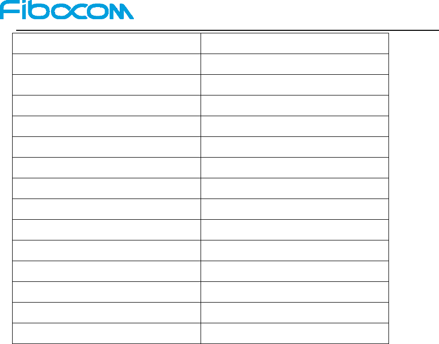
Operating Band
Antenna Gain(dBi)
GSM850
5.46
GSM1900
3
LTE-M1 BAND 2
9.5
LTE-M1 BAND 4
6.5
LTE-M1 BAND 12
12.94
LTE-M1 BAND 13
13.42
LTE-M1 BAND 26(814-824)
11.65
LTE-M1 BAND 26(824-849)
14.46
LTE-NB1 BAND 2
9.5
LTE-NB1 BAND 4
6.5
LTE-NB1 BAND 12
12.95
LTE-NB1 BAND 13
13.42
LTE-NB1 BAND 26(814-824)
11.65
LTE-NB1 BAND 26(824-849)
14.46
2) The transmitter module may not be co-located with any other transmitter or antenna.
As long as 2 conditions above are met, further transmitter test will not be required.
However, the OEM
integrator is still responsible for testing their end-product for any additional compliance
requirements
required with this module installed
IMPORTANT NOTE: In the event that these conditions can not be met (for example
certain laptop configurations or co-location with another transmitter), then the FCC
authorization is no longer considered valid and the FCC ID can not be used on the final
product. In these circumstances, the OEM integrator will be responsible for re-evaluating
the end product (including the transmitter) and obtaining a separate FCC authorization.
End Product Labeling
This transmitter module is authorized only for use in device where the antenna may be
installed such that 20 cm may be maintained between the antenna and users. The final
end product must be labeled in a visible area with the following: “Contains FCC ID:
ZMOM910GL”.The grantee's FCC ID can be used only when all FCC compliance
Host manufacturer is responsible for ensuring that the host continues to be compliant
with the Part 15 subpart B unintentional radiator requirements after the module is
installed and operational.

Reproduction forbidden without Fibocom Wireless Inc. written authorization - All Rights Reserved.
M910-GL Hardware User Manual Page 10 of 45
requirements are met.
Manual Information To the End User
The OEM integrator has to be aware not to provide information to the end user regarding
how to install or remove this RF module in the user’s manual of the end product which
integrates this module. The end user manual shall include all required regulatory
information/warning as show in this manual.
1.7 IC Statement
This device complies with Industry Canada license-exempt RSS standard(s). Operation is
subject to the following two conditions: (1) this device may not cause interference, and (2)
this device must accept any interference, including interference that may cause undesired
operation of the device.
Le présent appareil est conforme aux CNR d'Industrie Canada applicables aux appareils
radio exempts de licence. L'exploitation est autorisée aux deux conditions suivantes : (1)
l'appareil ne doit pas produire de brouillage, et (2) l'utilisateur de l'appareil doit accepter
tout brouillage radioélectrique subi, même si le brouillage est susceptible d'en
compromettre le fonctionnement.
Radiation Exposure Statement:
This equipment complies with IC radiation exposure limits set forth for an uncontrolled
environment. This equipment should be installed and operated with minimum distance
20cm between the radiator & your body.
Déclaration d'exposition aux radiations:
Cet équipement est conforme aux limites d'exposition aux rayonnements IC établies
pour un environnement non contrôlé. Cet équipement doit être installé et utilisé avec un
minimum de 20 cm de distance entre la source de rayonnement et votre corps.\
This Class B digital apparatus complies with Canadian ICES-003.
Cet appareil numérique de la classe B est conforme à la norme NMB-003 du Canada.
The Innovation, Science and Economic Development Canada certification label of a
module shall be clearly visible at all times when installed in the host device; otherwise,

Reproduction forbidden without Fibocom Wireless Inc. written authorization - All Rights Reserved.
M910-GL Hardware User Manual Page 11 of 45
the host device must be labeled to display the Innovation, Science and Economic
Development Canada certification number for the module, preceded by the words
“Contains transmitter module IC: 21374-M910GL
Reproduction forbidden without Fibocom Wireless Inc. written authorization - All Rights Reserved.
M910-GL Hardware User Manual Page 12 of 45
2 Product Overview
2.1 Product Introduction
The M910-GL is a multi-mode (LTE Cat.M1, LTE Cat.NB1 and EGPRS) IoT wireless
communication module that supports half-duplex LTE and GSM. It can provide data connection in
LTE-FDD, LTE-TDD, GPRS and EGPRS networks, and also supports GNSS and VOLTE (LTE
Cat.M1).
2.2 Product Specifications
Specification
Operating
frequency band
LTE FDD : B1/B2/B3/B4/B5/B8/B12/B13/B18/B19/B20/B26/B28
LTE TDD : B39 (Cat.M1 only)
GSM : GSM850/GSM900/DCS1800/PCS1900
Data transmission
LTE features
Support Cat.M1 and Cat.NB1
Cat.M1: The maximum uplink rate 375kbps, the
maximum downlink rate 375kbps
Cat.NB1: The maximum uplink rate 70kbps, the
maximum downlink rate 32kbps
GSM features
GPRS: the maximum downlink rate 107kbps, the
maximum uplink rate 85.6kbps
EDGE: The maximum downlink rate 296kbps, the
maximum uplink rate 236.8kbps
Power supply
voltage
3.3V~4.3V (3.8V recommended)
Temperature
Normal: -30°C~+75°C
Extended: -40°C ~+85°C
Storage: -40°C ~+85°C
Physical
characteristics
Package: LGA 120Pin
Size: 27.6×25.4×2.3 mm
Weight: TBD
Interface
Antenna
Antenna: Main x 1、GNSS x 1
Reproduction forbidden without Fibocom Wireless Inc. written authorization - All Rights Reserved.
M910-GL Hardware User Manual Page 13 of 45
Functional
interface
USIM 3.0V/1.8V
USB 2.0 x 1
UART, SIM, PCM, I2C
System Indicator
Clock
ADC
Software
Protocol Stack
Support PPP/TCP/UDP/SSL/TLS/FTP(S)/HTTP(S) protocols
AT Command
3GPP TS 27.007 and 27.005, and proprietary FIBOCOM AT
Firmware update
FOTA
Voice service
Support
SMS
Text and PDU mode; point-to-point SMS; SMS broadcast
MMS service
TBD
Note:
When the temperature is beyond the normal operating temperature range (-30 °C to +
75 °C), the RF performance of the module may slightly exceed the 3GPP specifications.
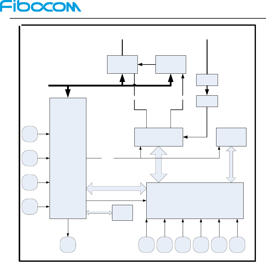
2.3 Hardware Diagram
Figure 2-1 hardware diagram shows the main hardware features of the M910-GL module.
PMIC
MCP
Clock
Function interface
Transceiver
RF PA
RF filter
RF switch
Reproduction forbidden without Fibocom Wireless Inc. written authorization - All Rights Reserved.
M910-GL Hardware User Manual Page 14 of 45
PMIC
Baseband
Control
19.2M
xo
Transceiver NAND
DDR2
IQ
POWER
GPIO Uarts PCM
IIS USIMIICUSBV180
LED
EMG_
RST
ADC
A_ON
2G PA+SWITCH LTE PA
BATT+
TX RX TX
LNA
SAW
RF_OUT GNSS_OUT
Figure 2-1 Hardware Diagram
Reproduction forbidden without Fibocom Wireless Inc. written authorization - All Rights Reserved.
M910-GL Hardware User Manual Page 15 of 45
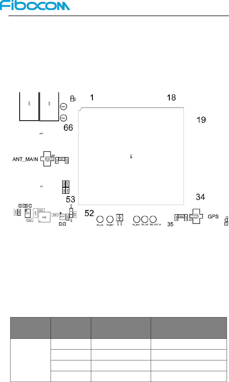
3 Application Interface
3.1 LGA Interface
M910-GL module adopts LGA packaging with a total of 120 pins. It can be applied to the client’s
wireless application platform. The function of interface:
Power supply
Power on/off, reset
interface
interface
interface
I2C interface
Status indication interface
Emergency download interface
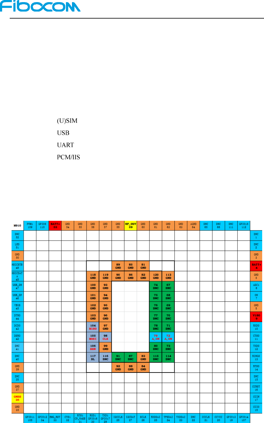
3.1.1 Pin Distribution
Figure 3-1 Pin Distribution Diagram
Reproduction forbidden without Fibocom Wireless Inc. written authorization - All Rights Reserved.
M910-GL Hardware User Manual Page 16 of 45
Note: It is recommended that the heat sink pad is reserved for the PCB packaging and
welded.
3.1.2 Pin definition
The pin definitions are as shown in the following table:
Pin
Pin Name
I/O
Level
Description
1
DNC
-
-
2
DNC
-
-
3
GND
G
-
Ground
4
BATT+
I
3.8V
RF PA power input(3.3V-4.3V)
5
GND
G
-
Ground
6
ADC
I
-
Analog input
7
ON
I
1.8V
High level power-on control pin;
can be floating
8
GND
G
-
Ground
9
V180
O
1.8V
Module digital level, 1.8V
output, 80mA
10
RXD0
I
1.8V
Serial interface signal
11
CTS0
O
1.8V
Serial interface signal
12
TXD0
O
1.8V
Serial interface signal
13
RING0
O
1.8V
Serial interface signal
14
RTS0
O
1.8V
Serial interface signal
15
DNC
-
-
16
CCRST
O
1.8V or 3.0V
SIM reset signal line
17
CCIN
O
1.8V
SIM card hot plug detection
18
CCIO
O
1.8V or 3.0V
SIM data signal line
107
GPIO14
I/O
1.8V
GPIO
19
GPIO13
I/O
1.8V
GPIO
20
CCVCC
O
1.8V or 3.0V
SIM power supply
21
CCCLK
O
1.8V or 3.0V
SIM clock signal line
22
DNC
-
23
TXDDAI
O
1.8V
Digital voice interface
24
TFSDAI
IO
1.8V
Digital voice interface
25
RXDDAI
I
1.8V
Digital voice interface

Reproduction forbidden without Fibocom Wireless Inc. written authorization - All Rights Reserved.
M910-GL Hardware User Manual Page 17 of 45
Pin
Pin Name
I/O
Level
Description
26
SCLK
I/O
1.8V
Digital voice interface
27
I2CDAT
OD
-
I2C interface data signal
28
I2CCLK
OD
-
I2C interface clock signal
29
TXD1
O
1.8V
Serial interface signal
30
RXD1
I
1.8V
Serial interface signal
31
RTS1
O
1.8V
Serial interface signal
32
CTS1
O
1.8V
Serial interface signal
33
EMG_RST
I
1.8V
Module reset signal
34
GPIO12
I/O
1.8V
GPIO
108
GPIO11
I/O
1.8V
GPIO
35
GND
G
-
Ground
36
GNSS
I
-
GNSS antenna interface
37
GND
G
-
Ground
38
DNC
-
-
39
GND
G
-
Ground
40
DNC
-
-
41
DNC
-
-
42
DSR0
43
DCD0
O
1.8V
Serial interface signal
44
DTR0
I
1.8V
Serial interface signal
45
VBUS
I
1.8V
USB plug detect signal
46
USB_DP
I/O
USB 2.0
Specification
USB differential data positive
signal
47
USB_DM
I/O
USB 2.0
Specification
USB differential data negative
signal
48
DNC
-
-
49
DNC
-
-
50
GND
G
-
Ground
51
LED
OD
-
Network indicator
52
DNC
-
-
109
PWM1
O
1.8V
Adjustable pulse signal
110
GPIO8
I/O
1.8V
GPIO
53
BATT+
I
3.8V
PMIC power input(3.3V-4.3V)
Reproduction forbidden without Fibocom Wireless Inc. written authorization - All Rights Reserved.
M910-GL Hardware User Manual Page 18 of 45
Pin
Pin Name
I/O
Level
Description
54
GND
G
-
Ground
55
GND
G
-
Ground
56
GND
G
-
Ground
57
GND
G
-
Ground
58
GND
G
-
Ground
59
RF_OUT
I/O
Main antenna interface
60
GND
G
-
Ground
61
GND
G
-
Ground
62
GND
G
-
Ground
63
GND
G
-
Ground
64
GND
G
-
Ground
65
DNC
-
-
66
DNC
-
-
111
DNC
-
-
112
GPIO15
I/O
1.8V
GPIO
67
DNC
-
-
68
DNC
-
-
69
DNC
-
-
70
DNC
-
-
71
DNC
-
-
72
A_ON
I
1.8V
Power on/off signal; low level
power on /off
73
DNC
-
-
74
DNC
-
-
75
DNC
-
-
76
DNC
-
-
77
DNC
-
-
78
DNC
-
-
79
A_ON
I
1.8V
Power on/off signal; low level
power on /off
80
DNC
-
-
81
GND
G
-
Ground
82
GND
G
-
Ground

Reproduction forbidden without Fibocom Wireless Inc. written authorization - All Rights Reserved.
M910-GL Hardware User Manual Page 19 of 45
Pin
Pin Name
I/O
Level
Description
83
GND
G
-
Ground
84
GND
G
-
Ground
85
GND
G
-
Ground
86
GND
G
-
Ground
87
DNC
-
-
88
GND
G
-
Ground
89
GND
G
-
Ground
90
GND
G
-
Ground
91
DNC
-
-
92
GND
G
-
Ground
93
GND
G
-
Ground
94
GND
G
-
Ground
95
GND
G
-
Ground
96
GND
G
-
Ground
97
GND
G
-
Ground
98
DNC
-
-
CLK
99
GND
G
-
Ground
100
GND
G
-
Ground
101
GND
G
-
Ground
102
GND
G
-
Ground
103
GND
G
-
Ground
104
DNC
-
-
MISO
105
DNC
-
-
MOSI
106
DNC
-
-
SSN
113
GND
G
-
Ground
114
DNC
-
-
115
DNC
-
-
116
DNC
-
-
117
DL
I
1.8V
Emergency download point
118
GND
G
-
Ground
119
GND
G
-
Ground
120
GND
G
-
Ground
Reproduction forbidden without Fibocom Wireless Inc. written authorization - All Rights Reserved.
M910-GL Hardware User Manual Page 20 of 45
Note:
DNC pins remain floating.
3.2 Power Supply
The power interfaces of M910-GL module are as shown in the following table:
Pin Name
I/O
Pin
Description
BATT+
I
4,53
Module power supply, 3.3 ~
4.3, nominal value 3.8V
V180
O
9
Voltage Output, 1.8V, 80mA
GND
-
Ground
3.2.1 Power Supply
The power supply range of the M910-GL module is 3.3V-4.3V.
While ensuring the sufficient BATT + power supply capacity (2A load), the design shall follow:
Connect a 100uF low-ESR (less than 0.5Ω) ceramic voltage-stabilizing capacitor near the BATT +
input. Since the price of small sized high-capacity ceramic capacitor is higher, it is recommended
to replace it with a 220uF tantalum capacitor, and then connect a 0.1uF ~ 1uF ceramic capacitor.
3.2.2 1.8V Output
The M910-GL outputs a 1.8V voltage using for the internal digital circuit of the module. The
voltage is the IO level voltage of the module and can be used to indicate that the module is on or
off, or for external low current (<80mA) circuit. If it is not in use, keep it in floating status. The
logic level of V180 is defined as follows:
Parameter
Minimum
Typical
Maximum
Unit
V180
1.71
1.8
1.89
V
VIH
1.3
1.8
1.89
V
VIL
-0.3
0
0.5
V
3.2.3 Power consumption
In the case of 3.8V power supply , the power consumption of M910-GL module is shown in the
following table:
Reproduction forbidden without Fibocom Wireless Inc. written authorization - All Rights Reserved.
M910-GL Hardware User Manual Page 21 of 45
Parameter
Mode
Condition
Average
Typ.Current(m
A)
Ioff
Power off
Module power off
0.008
Isleep
PSM
0.01
e-DRX
TBD
Iidle
RRC_Idle
<5mA
RRC_Connect
<42 mA
IGPRS-RMS
CS4
GPRS
GPRS Data transfer GSM850; PCL=5; 1Rx/4Tx
513
GPRS Data transfer GSM900; PCL=5; 1Rx/4Tx
510
GPRS Data transfer DCS1800; PCL=0;
1Rx/4Tx
409
GPRS Data transfer PCS1900; PCL=0; 1Rx/4Tx
381
IEGPRS-RMS
MCS9
EDGE
EDGE Data transfer GSM850; PCL=8; 1Rx/4Tx
437
EDGE Data transfer GSM900; PCL=8; 1Rx/4Tx
468
EDGE Data transfer DCS1800; PCL=2;
1Rx/4Tx
400
EDGE Data transfer PCS1800; PCL=2;
1Rx/4Tx
383
ILTE-RMS
LTE FDD
LTE FDD B1 @+23dBm
Cat.M1: 222
Cat.NB1: 272
LTE FDD B2 @+23dBm
Cat.M1: 223
Cat.NB1: 304
LTE FDD B3 @+23dBm
Cat.M1: 218
Cat.NB1: 336
LTE FDD B4 @+23dBm
Cat.M1: 216
Cat.NB1: 332
LTE FDD B5 @+23dBm
Cat.M1: 224
Cat.NB1: 267
LTE FDD B8 @+23dBm
Cat.M1: 241
Cat.NB1: 275
LTE FDD B12 @+23dBm
Cat.M1: 249
Cat.NB1: 308
LTE FDD B13 @+23dBm
Cat.M1: 229
Cat.NB1: 282
LTE FDD B17 @+23dBm @NB only
Cat.NB1: 306
LTE FDD B18 @+23dBm
Cat.M1: 221
Cat.NB1: 262
Reproduction forbidden without Fibocom Wireless Inc. written authorization - All Rights Reserved.
M910-GL Hardware User Manual Page 22 of 45
Parameter
Mode
Condition
Average
Typ.Current(m
A)
LTE FDD B19 @+23dBm
Cat.M1: 221
Cat.NB1: 263
LTE FDD B20@+23dBm
Cat.M1: 219
Cat.NB1: 253
LTE FDD B26@+23dBm
Cat.M1: 220
Cat.NB1: 279
LTE FDD B28@+23dBm
Cat.M1: 245
Cat.NB1: 298
LTE TDD
LTE TDD B39 @+23dBm @eMTC only
Cat.M1: TBD
Note:
PSM: The M910-GL module can further reduce its own power consumption by entering the
PSM. PSM is similar to switch off, but the module is still registered on the network. After
waking up from PSM mode, the module does not need to reattach or reestablish a PDN
connection. Therefore, after the module enters the PSM, it can not immediately respond to
user requests. When the module needs to use the PSM, it will request an activity time value
during each attach and TAU process. If the network side supports PSM and accepts the
module to use the PSM, then the network confirms PSM usage by assigning the module an
activity time value. If the module wants to change the activity time value, for example
when the conditions in the module change, the module will request the desired value during
the TAU.
If the network side supports PSM, PSM function can be enabled by AT command.
Wake up the module from the PSM state as follows:
1. Pull PWRKEY pin to low level to wake up the module;
2. Wait for the timer (T3412) overflow, the module will automatically wake up.
3.3 Control Signal
The M910-GL module provides two control signals for power on/off and reset operations. The pin
definitions are as follows:
Pin name
I/O
Pin
Description
EMG_RST
I
33
When the module is in work, give it a Tst (150 ~ 460ms) low level,
and then pull it high, the module is reset
Reproduction forbidden without Fibocom Wireless Inc. written authorization - All Rights Reserved.
M910-GL Hardware User Manual Page 23 of 45
A_ON
I
72\79
When pulling down the level to power on, the shortest duration of
low level is 100ms, and when pulling down the level to power off,
the minimum duration is 2s
3.3.1 Module start-up
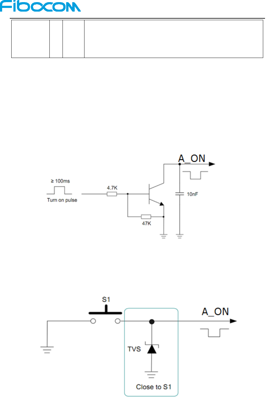
3.3.1.1.1 Start-up circuit reference
When the M910-GL module is in shutdown mode, the module will start up by pulling down A_ON for
at least 100ms. It is recommended to use open-drain drive circuit for control. The reference circuit is
shown in Figure 3-2:
Figure 3-2 Open Set Reference Start-up Circuit
Another control method is to directly control through a button, and place a TVS near the button
for ESD protection. The reference circuit is shown in Figure 3-3:
Figure 3-3 Button Start-up Reference Circuit
Reproduction forbidden without Fibocom Wireless Inc. written authorization - All Rights Reserved.
M910-GL Hardware User Manual Page 24 of 45
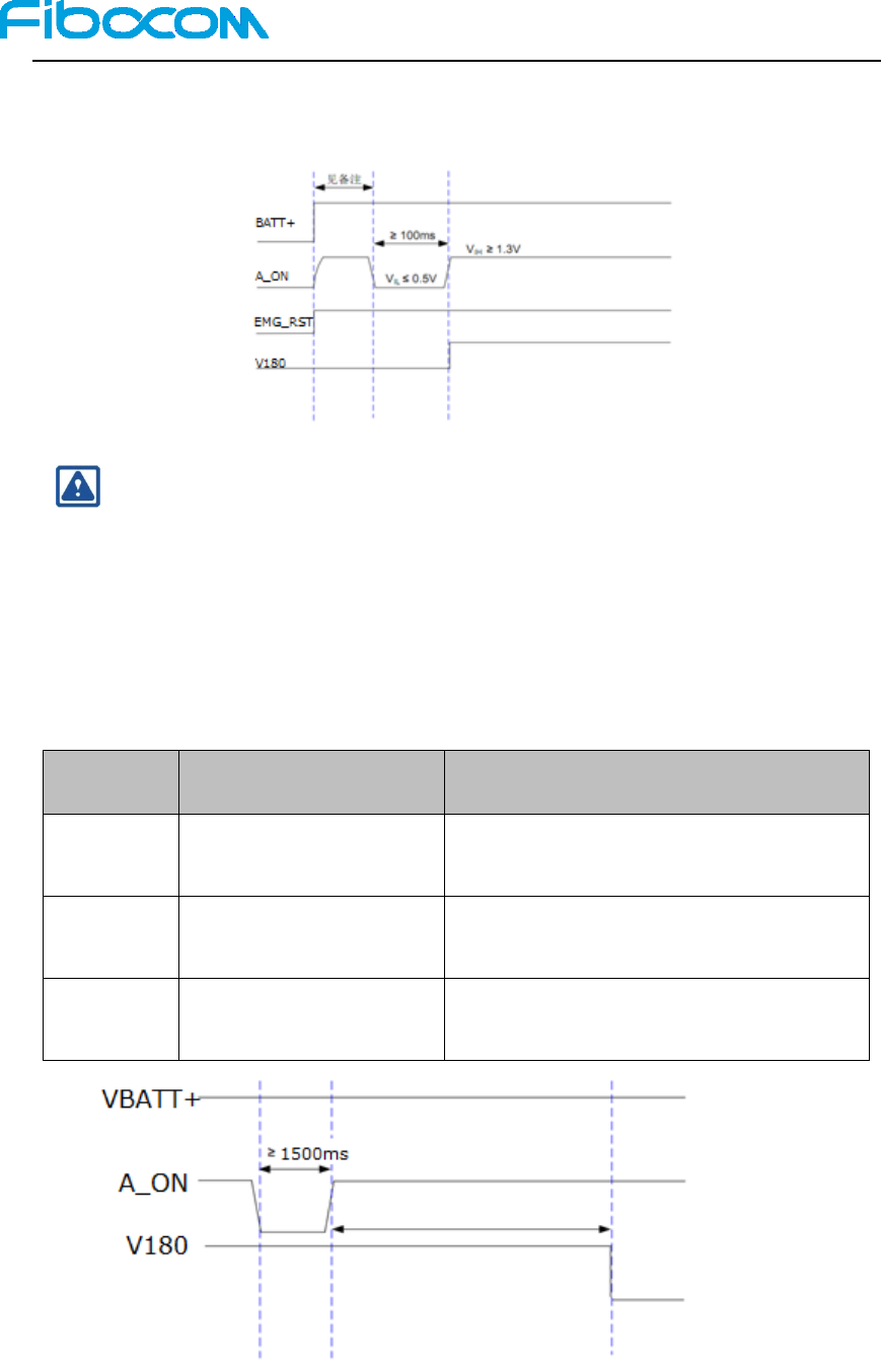
3.3.1.2 Start-up timing
The start-up timing is shown in Figure 3-4:
Figure 3-4 Start-up Timing Control Diagram
Note:
Before pulling down the A_ON pin, make sure the BATT + voltage is stable. It is
recommended that the interval between powering up BATT + and pulling down A_ON pin
should not be less than 100ms.
3.3.2 Module shutdown
The module supports the following three shutdown modes:
Shutdown
Mode
Shutdown Method
Applicable scenarios
Low-voltage
shutdown
When BATT + powers down,
the module will shut down
The module does not shut down through normal
process, i.e. logout process from the base station
Hardware
shutdown
Pull down A_ON (more
than1. 5s)
Normal shutdown
AT shutdown
TBD
Figure 3-5 Shutdown Timing Control Diagram
Reproduction forbidden without Fibocom Wireless Inc. written authorization - All Rights Reserved.
M910-GL Hardware User Manual Page 25 of 45
3.3.2.1 Shutdown Timing
1. When the module is working properly, do not cut off the power to the module immediately to
avoid damaging the internal Flash of the module. It is strongly recommended to shut down the
module by A_ON or AT command before disconnecting the power supply.
2. When using the AT command to shut down, make sure that the A_ON is in a high level state
after the shutdown command is executed, otherwise the module will start up again after the
shutdown is completed.
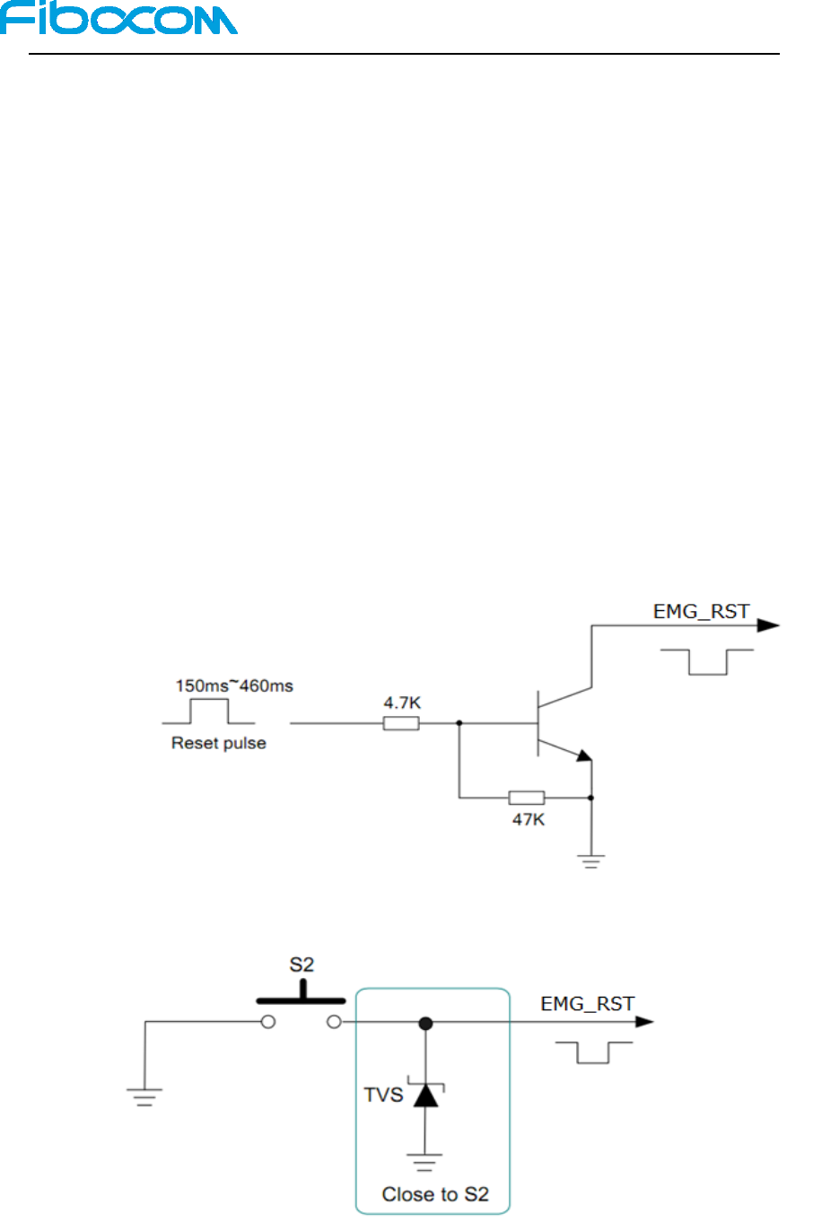
3.3.3 Module reset
M910-GL module can reset by hardware and AT command.
3.3.3.1 Reset circuit
Refer to Figure 3-6 and Figure 3-7. It is similar to the start-up/shutdown control circuit. The client
can control the EMG_RST pin using an open-drain drive circuit or push button.
Figure 3-6 EMG_RST Reset Open Reference Circuit
Figure 3-7 EMG_RST Reset Button Reference Circuit
Reproduction forbidden without Fibocom Wireless Inc. written authorization - All Rights Reserved.
M910-GL Hardware User Manual Page 26 of 45
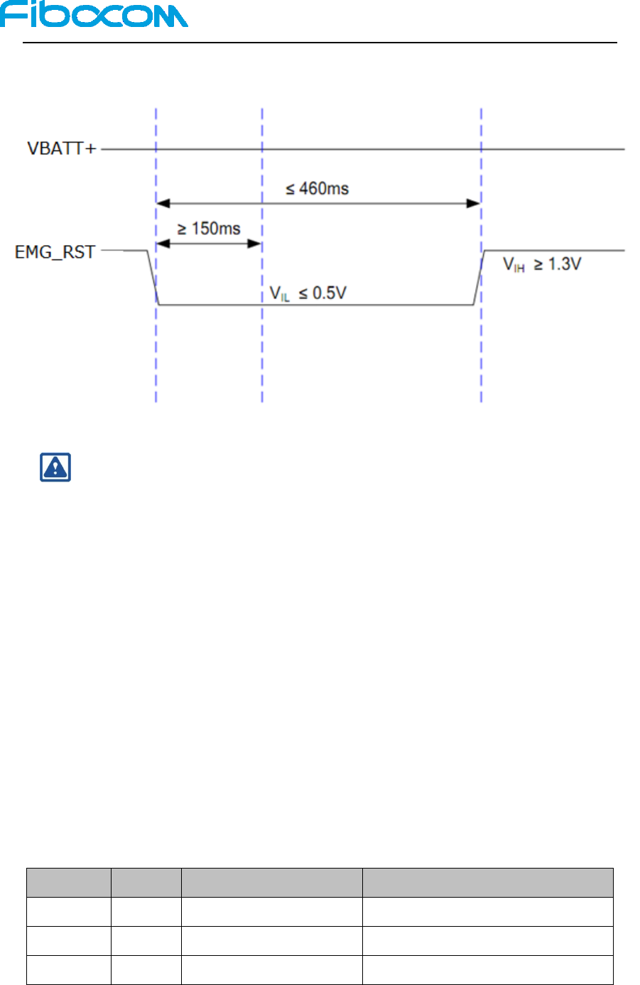
3.3.3.2 RESET control timing
Figure 3-8 Reset Control Timing
Note:
RESET is a sensitive signal, so it is recommended to add a filter capacitor close to the
module. In case of PCB layout, the RESET signal lines should keep away from the RF
interference and be protected by nice Ground. Also, the RESET signal lines shall be
neither near the PCB edge nor route on the surface planes to avoid module from reset
caused by ESD problems.
Software reset: TBD
3.4 USB Interface
The M910-GL provides a USB interface that conforms to the USB 2.0 specification and supports
high-speed (480Mbps) and full-speed (12Mbps) modes. The USB interface can be used for AT
command transmission, data transmission, software debugging and software upgrades.
For more information about the USB 2.0 specification, visit http://www.usb.org/home.
3.4.1 USB interface definition
Pin Name
I/O
Pin
Description
USB_DN
I/O
47
USB differential data bus
USB_DP
I/O
46
USB differential data bus
VBUS
I
45
USB plug detection; 1.8V input level
We recommend that clients reserve USB interface for software upgrades.
Reproduction forbidden without Fibocom Wireless Inc. written authorization - All Rights Reserved.
M910-GL Hardware User Manual Page 27 of 45
In the design of USB interface circuit, in order to ensure the USB performance, the following
principles are recommended in circuit design:
1) The USB data lines need to be grounded, with 90Ω impedance differential cable;
2) Do not take the USB cable under the crystal, oscillator, magnetic device or RF signal. It is
recommended to take the inner differential cable and the cable shall be grounded at all directions;
3) The model selection for ESD protection of USB data cable requires special attention, and the
parasitic capacitance must not exceed 2pF;
4) ESD protector of USB should be placed close to the USB interface.
5) As a USB plug-in testing, the input level of VBUS does not exceed 1.8V, and VBUS connects
USB USB_VBUS pin through the partial pressure resistor.
3.5 USIM Interface
M910-GL module supports the USIM card interface (1.8V and 3.0V cards).
3.5.1 USIM pin
USIM pin is shown in the following table:
Pin Name
I/O
Pin
Description
CCRST
I/O
15
RESET Signal
CCIN
(USIM_DET)
O
17
Detect USIM/SIM card
for Hot-swap
CCIO
O
18
Data Signal
CCVCC
O
20
Power
CCCLK
I
21
Clock Signal
3.5.2 USIM interface circuit
3.5.2.1 SIM card slot with detection signal
USIM/SIM design requires the use of SIM card slot (Fibocom recommend: SIM016-8P-220P). We
recommend using hot plug holder with SIM_DECTECT feature.
Reproduction forbidden without Fibocom Wireless Inc. written authorization - All Rights Reserved.
M910-GL Hardware User Manual Page 28 of 45
Figure 3-9 SIM Card Slot Diagram SIM016-8P-220P
Figure 3-10 M910-GL USIM/SIM Interface with Detection Reference Design
Reproduction forbidden without Fibocom Wireless Inc. written authorization - All Rights Reserved.
M910-GL Hardware User Manual Page 29 of 45
Principles of SIM card slot with detection signal are as follows:
SIM card is plugged, CCIN is high level
SIM card is unplugged, CCIN is low level
For SIM card slot without detection signal, CCIN remains floating.
Note:
SIM card hot plug feature can be enabled by AT command for logic level control. Please
refer to the AT command manual for the specific AT command.
3.5.3 USIM design requirements
SIM card circuit design shall meet EMC standards and ESD requirements, and at the same time, it
shall improve anti-interference ability to ensure that the SIM card can work stably. The design
needs to strictly observe the following rules:
SIM card slot is placed as close to the module as possible, away from the RF antenna, DCDC
power, clock signal lines and other strong interference sources;
Adopt the SIM card slot with metal shield shell to improve anti-interference ability;
The length of cable from the module to the SIM card slot shall not exceed 100mm. Longer
cable reduces signal quality.
CCCLK and CCIO signals are isolated to avoid mutual interference. If it is difficult to do so,
SIM signal needs to be protected as a set;
The filter capacitor and ESD device of SIM card signal cable are placed close to the SIM
card slot. Select 22 ~ 33pF capacitor for ESD device equivalent capacitor.
3.6 UART Interface
3.6.1 UART interface definition
M910-GL module has two serial interfaces: serial interface 0 and serial interface 1. The following
describes the main features of these two serial interfaces:
Support 4800bps, 9600bps, 19200bps, 38400bps, 57600bps, 115200bps, 230400bps,
460800bps, 921600bps baud rate, and the default baud rate is 115200bps, used for data
transmission and AT command transmission.
The following table describes the serial interface 0 pin:
Pin Name
I/O
Pin
Description
RXD0
I
10
Serial interface RXD
CTS0
DO
11
Serial interface CTS
TXD0
O
12
Serial interface TXD
RING0
DO
13
Serial interface RI
Reproduction forbidden without Fibocom Wireless Inc. written authorization - All Rights Reserved.
M910-GL Hardware User Manual Page 30 of 45
Pin Name
I/O
Pin
Description
RTS0
DI
14
Serial interface RTS
DSR0
DO
42
Serial interface DSR
DCD0
DO
43
Serial interface DCD
DTR0
DI
44
Serial interface DTR
The following table describes the serial interface 1 pin:
Pin Name
I/O
Pin
Description
TXD1
DO
29
Serial interface TXD
RXD1
DI
30
Serial interface RXD
RTS1
DI
31
Serial interface RTS
CTS1
DO
32
Serial interface CTS
3.6.2 UART interface application
The serial interface level of M910-GL module is 1.8V. If the level of the client host system is 3.3V
or other, a level shifter shall be added to the serial interface connection between the module and
the host. The following figure shows the reference circuit design using level shifter chip:
Figure 3-11 UART Signal Connection 1
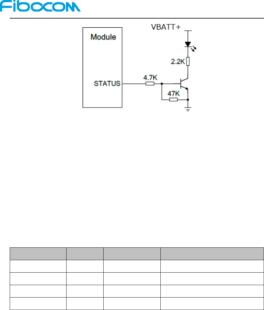
3.7 Status Indicator
M910-GL module provides a signal to indicate the operating status of the module, and status
indicator pin is shown in the following table:
Pin Name
I/O
Pin
Description
LED
O
51
TBD
LED reference circuit is shown in Figure 3-12:
Reproduction forbidden without Fibocom Wireless Inc. written authorization - All Rights Reserved.
M910-GL Hardware User Manual Page 31 of 45
Figure 3-12: M910-GL LED Reference Design Diagram
3.8 PCM/IIS
The M910-GL provides a digital voice interface for communication with digital audio devices
such as external CODECs.
RXDDAI data sends the external CODEC MIC to the DSP code channel inside the module; the
TXDDAI signal is sent from the internal DSP code channel to the external CODEC Speaker.
M910-GL main chip provides PCM/IIS signal using the mainstream European E1 standard.
3.8.1 Digital voice interface definition
PIN Name
I/O
PIN Num.
Description
TXDDAI
I
23
Digital voice output signal
TFSDAI
O
24
Digital voice synchronization signal
RXDDAI
I
25
Digital voice input signal
SCLK
O
26
Digital voice clock signal
3.8.2 Interface description
TBD
3.8.3 Signal description
TBD
3.9 ADC function
TBD
Reproduction forbidden without Fibocom Wireless Inc. written authorization - All Rights Reserved.
M910-GL Hardware User Manual Page 32 of 45
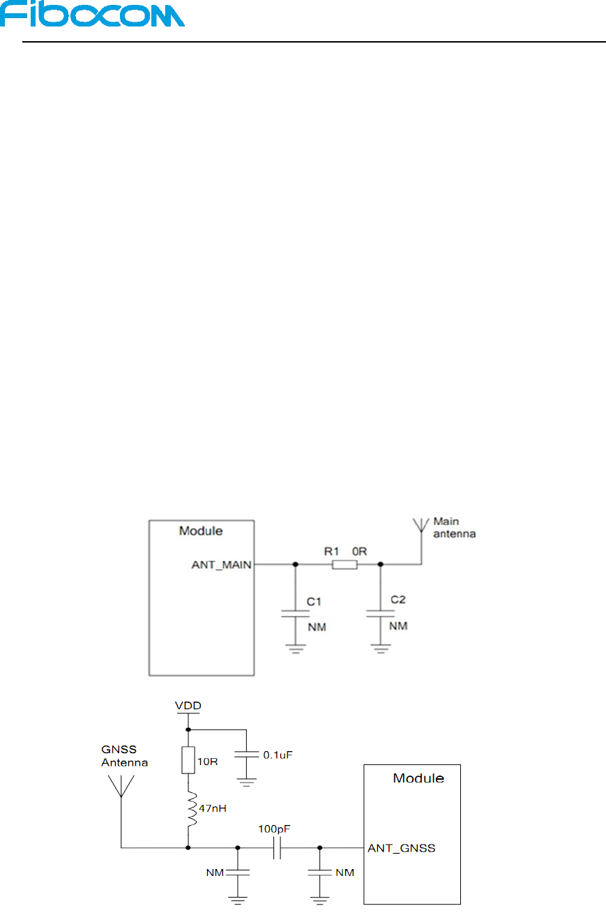
4 Antenna Interface
M910-GL provides two antenna interfaces:
MAIN Connector50Ω impedance
GNSS Connector50Ω impedance
4.1 Antenna design
4.1.1 Antenna RF connector
M910-GL has two antennas, led by welding plate.
Antenna is a sensitive device, susceptible to the external environment. For example, the size of the
module, the location of the antenna, the space it occupies, and the surrounding ground all may
affect antenna performance. In addition, the RF cable connecting the antenna, and the location of
the fixed antenna also may affect the performance of the antenna.
The figure below shows the reference circuit design of the main antenna and GNSS antenna.
These matches need to be placed close to the antenna:
Figure 4-1 RF Reference Circuit Design
The module has no special requirements for the type of antenna. The user can adjust the antenna
Reproduction forbidden without Fibocom Wireless Inc. written authorization - All Rights Reserved.
M910-GL Hardware User Manual Page 33 of 45
gain, antenna size, shape, TRP, TIS, according to the actual structure of the whole machine,
combined with the net space environment.
Figure 4-2 ANT Reference layout Design
Make sure the characteristic impedance of the transmission line is 50 ohms.
Since the antenna loss should be less than 0.3dB, keep the PCB cable as short as possible.
PCB cable should have a good reference ground to avoid other signal cable near the antenna.
Recommend a complete ground, and use this complete ground as a reference ground.
4.1.2 RF output power of M910-GL
The RF output power of M910-GL is shown in the following table.
Network
mode
Band
Max
Min
GSM
GSM850
32.5 dBm±1dB
5dBm±3.5dB
EGSM900
32.5 dBm±1dB
5dBm±3.5dB
DCS1800
29.5dBm±1dB
0dBm±3.5dB
PCS1900
29.5dBm±1dB
0dBm±3.5dB
Reproduction forbidden without Fibocom Wireless Inc. written authorization - All Rights Reserved.
M910-GL Hardware User Manual Page 34 of 45
Network
mode
Band
Max
Min
TDD-LTE
Band39
TBD
TBD
FDD-LTE
Band1
23dBm±1dB
<-44dBm
Band2
23dBm±1dB
<-44dBm
Band3
23dBm±1dB
<-44dBm
Band4
23dBm±1dB
<-44dBm
Band5
23dBm±1dB
<-44dBm
Band8
23dBm±1dB
<-44dBm
Band12
23dBm±1dB
<-44dBm
Band13
23dBm±1dB
<-44dBm
Band18
23dBm±1dB
<-44dBm
Band19
23dBm±1dB
<-44dBm
Band20
23dBm±1dB
<-44dBm
Band26
23dBm±1dB
<-44dBm
Band28
23dBm±1dB
<-44dBm
4.1.3 RF receiving sensitivity of M910-GL
Network mode
Band
Sensitive(dbm)
GSM(8-PSK)
GSM850
-86
EGSM900
-86
DCS1800
-86
PCS1900
-86
Network
mode
Band
Cat.M1
Sensitive/3GPP(dbm)-5MHz
Nb-iot
Sensitive/3GPP(dbm)
TDD-LTE
Band39
TBD
no support
FDD-LTE
Band1
-99.8/-102.3
-116/-107.5
Band2
-100.3/-100.3
-115.6/-107.5
Band3
-100.6/-99.3
-114.5/-107.5
Band4
-99.6/-102.3
-115.8/-107.5
Band5
-100.6/-100.8
-117.4/-107.5
Reproduction forbidden without Fibocom Wireless Inc. written authorization - All Rights Reserved.
M910-GL Hardware User Manual Page 35 of 45
Network
mode
Band
Cat.M1
Sensitive/3GPP(dbm)-5MHz
Nb-iot
Sensitive/3GPP(dbm)
Band8
-100.9/-99.8
-116.2/-107.5
Band12
-101.9/-99.3
-118.4/-107.5
Band13
-101.2/-99.3
-117.7/-107.5
Band18
-101.2/-102.3
-117.2/-107.5
Band19
-101/-102.3
-117.2/-107.5
Band20
-101.5/-99.8
-117.3/-107.5
Band26
-100.8/-100.3
-116.7/-107.5
Band28
-101.2/-100.8
-117.5/-107.5
4.1.4 Operating frequency of M910-GL supported bands (MHz)
Network mode
Band
Receive
Transmit
GSM
GSM850
869~894
824~849
EGSM900
925~960
880~915
DCS1800
1805~1880
1710~1785
PCS1900
1930~1990
1850~1910
TDD-LTE
Band39
1880~1920
1880~1920
FDD-LTE
Band1
2110~2170
1920~1980
Band2
1930~1990
1850~1910
Band3
1805~1880
1710~1785
Band4
2110~2155
1710~1755
Band5
869~894
824~849
Band8
925~955
880~910
Band12
728~746
699~716
Band13
746~757
777~787
Band18
860~874.9
815~829.9
Band19
875~889.9
830~844.9
Band20
791~821
832~862
Band26
859~893.9
814~848.9
Band28
758~803
703~748

Reproduction forbidden without Fibocom Wireless Inc. written authorization - All Rights Reserved.
M910-GL Hardware User Manual Page 36 of 45
4.2 Antenna Design
4.2.1 Antenna design requirements
1) Antenna efficiency
Antenna efficiency is the ratio of antenna input power to radiated power. Due to the antenna return
loss, material loss, and coupling loss, the radiated power is always lower than the input power.
Recommend> 40% (-4dB).
2) S11 or VSWR
S11 shows that the matching degree of the antenna’s 50 ohm impedance, to a certain extent,
affects the antenna efficiency. VSWR test methods can be used to measure this parameter.
Recommend S11 <-10dB.
3) Polarization
Polarization is the rotation direction of the electric field in the maximum radiation direction of the
antenna.
It is recommended to use linear polarization.
4) Radiation pattern
Radiation pattern refers to the antenna’s electromagnetic field strength in the far field in all
directions. Half-wave dipole antenna is the most suitable terminal antenna. For built-in antenna,
PIFA antennas or IFA antennas are recommended:
Antenna area: 6mm high*10mm wide*100mm long.
Antenna radiation direction: Omni_directional.
5) Gain and directivity
Antenna directivity refers to the electromagnetic field strength of electromagnetic wave in all
directions. Gain is a collection of antenna benefits and antenna directivity.
Recommended antenna gain ≤2.5dBi.
6) Interference
In addition to the antenna performance, other interferences on the PCB also may affect the
performance of the module. In order to ensure the high performance of the module, interference
must be controlled. Suggestions: For example, LCD, CPU, FPC cable, audio circuit, power supply
should be as far as possible away from the antenna, and make the appropriate isolation and
shielding, or filtering on the path.
7) Antenna index requirements
M910-GL module main antenna requirements
Frequency range
It shall use the most suitable antenna to adapt
Reproduction forbidden without Fibocom Wireless Inc. written authorization - All Rights Reserved.
M910-GL Hardware User Manual Page 37 of 45
M910-GL module main antenna requirements
to the relevant frequency band
Bandwidth (GPRS/EDGE)
Bandwidth (LTE)
Impedance
50 ohms
Input power
Standing wave ratio recommended
5 Electrical Characteristics
5.1 Limiting voltage range
The limiting voltage range refers to the power voltage of the module and the maximum voltage
range that the digital and analog input/output interface can withstand. Working outside this range
may cause damage to the product.
The voltage range of M910-GL is shown in the following table.
Parameter
Description
Min
Typ
Max
Unit
Reproduction forbidden without Fibocom Wireless Inc. written authorization - All Rights Reserved.
M910-GL Hardware User Manual Page 38 of 45
Parameter
Description
Min
Typ
Max
Unit
BATT+
Power supply
3.3
3.8
4.3
V
RMS average supply current
0
0.5
A
The IVBAT peak current may
reach 2A (power transmission
at each 4.6ms slot) at the
instantaneous voltage drop in
each time slot
400
mV
GPIO
Digital IO level supply
voltage
-0.3
1.8
2.0
V
Supply voltage in shutdown
mode
-0.25
0.25
V
5.2 Environment temperature range
M910-GL module is recommended to operate at -30~+75℃. It is recommended that the
application uses temperature control measures under harsh environmental conditions. At the same
time, the limited operating temperature range of the module should be provided. Under these
temperature conditions, some RF parameters may exceed the limit. It is recommended that the
module application terminal be stored in certain temperature conditions. Modules outside this
range may not operate or may be damaged.
Temperature
Min
Typ
Max
Unit
Operating
temperature
-30
25
75
℃
Limited operating
temperature
-40
85
℃
Storage temperature
-40
85
℃
5.3 Electrical characteristics of the interface in
operating status
VL: logic low level;
VH: logic high level;
Signal
VL
VH
Unit
Min
Max
Min
Max
Reproduction forbidden without Fibocom Wireless Inc. written authorization - All Rights Reserved.
M910-GL Hardware User Manual Page 39 of 45
Digital
input
-0.3
0.3*Vpin_min
0.3*Vpin_max
Vpin_max
V
Digital
output
GND
0.2
Vpin_min-0.2
Vpin
V
Note: Vpin_min = 1.45V, Vpin_max = 2.0V (Vpin is digital interface high level, Vpin = 1.8V)
Parameter
I/O
Min
Typ
Max
Unit
BATT+
I
3.3
3.8
4.3
V
CCVCC
O
1.7/2.75
1.8/2.85
1.9/2.95
V
5.4 Environmental reliability requirements
Test items
Test conditions
Low
temperature
storage test
Temperature -40℃±3 ℃, 24 hours in shutdown state
High
temperature
storage test
Temperature +85℃±3 ℃, 24 hours in shutdown state
Temperature
shock test
In shutdown state, 0.5 hour at -40℃ and +85℃ environment respectively,
the temperature conversion time <3min, for 24 cycles
High
temperature
and humidity
test
Temperature +85℃±3 ℃, humidity 90 ~ 95% RH, 24 hours in shutdown state
Low
temperature
operating test
Temperature -30℃±3 ℃, 24 hours in operating state
High
temperature
operating test
Temperature +75℃±3 ℃, 24 hours in operating state
Vibration test
Conduct vibration test according to the requirements shown in the table
below:
Frequency
Random vibration ASD (Acceleration Spectral
Density)
5~20Hz
0.96m2/s3
Reproduction forbidden without Fibocom Wireless Inc. written authorization - All Rights Reserved.
M910-GL Hardware User Manual Page 40 of 45
Test items
Test conditions
20~500Hz
0.96m2/s3(20Hz), other -3dB/octave
Connector life
test
50 times of insertion/removal for board to board connector interface; 30 times
of insertion/removal for RF antenna interface cable
ESD test
1 Test module antenna interface, power PAD and large ground area in call
state, ESD should meet the following conditions:
1) Contact discharge should pass ± 0.5KV test
2) Air discharge should pass ± 2KV test
2. Test EVB SIM card slot while the module is in shutdown state, ESD should
meet the following conditions:
1) Contact discharge should pass ± 0.5KV test
2) Air discharge should pass ± 2KV test
5.5 ESD characteristics
M910-GL is a consumer product. Although the design of the module has considered the ESD issue
and provided ESD protection, the ESD issue may occur in the transport and secondary
development, so developers should consider ESD protection for the final product. In addition to
considering anti-static treatment for packaging, please refer to recommended circuit for interface
design in the document for client’s application.
Refer to the following table for the ESD allowable discharge range of the M910-GL module.
Part
Air discharge
Contact discharge
BATT+,GND
±2KV
±0.5KV
Antenna port
± 8KV
Other port
±2KV
±0.5KV
Reproduction forbidden without Fibocom Wireless Inc. written authorization - All Rights Reserved.
M910-GL Hardware User Manual Page 41 of 45
6 Structure Specification
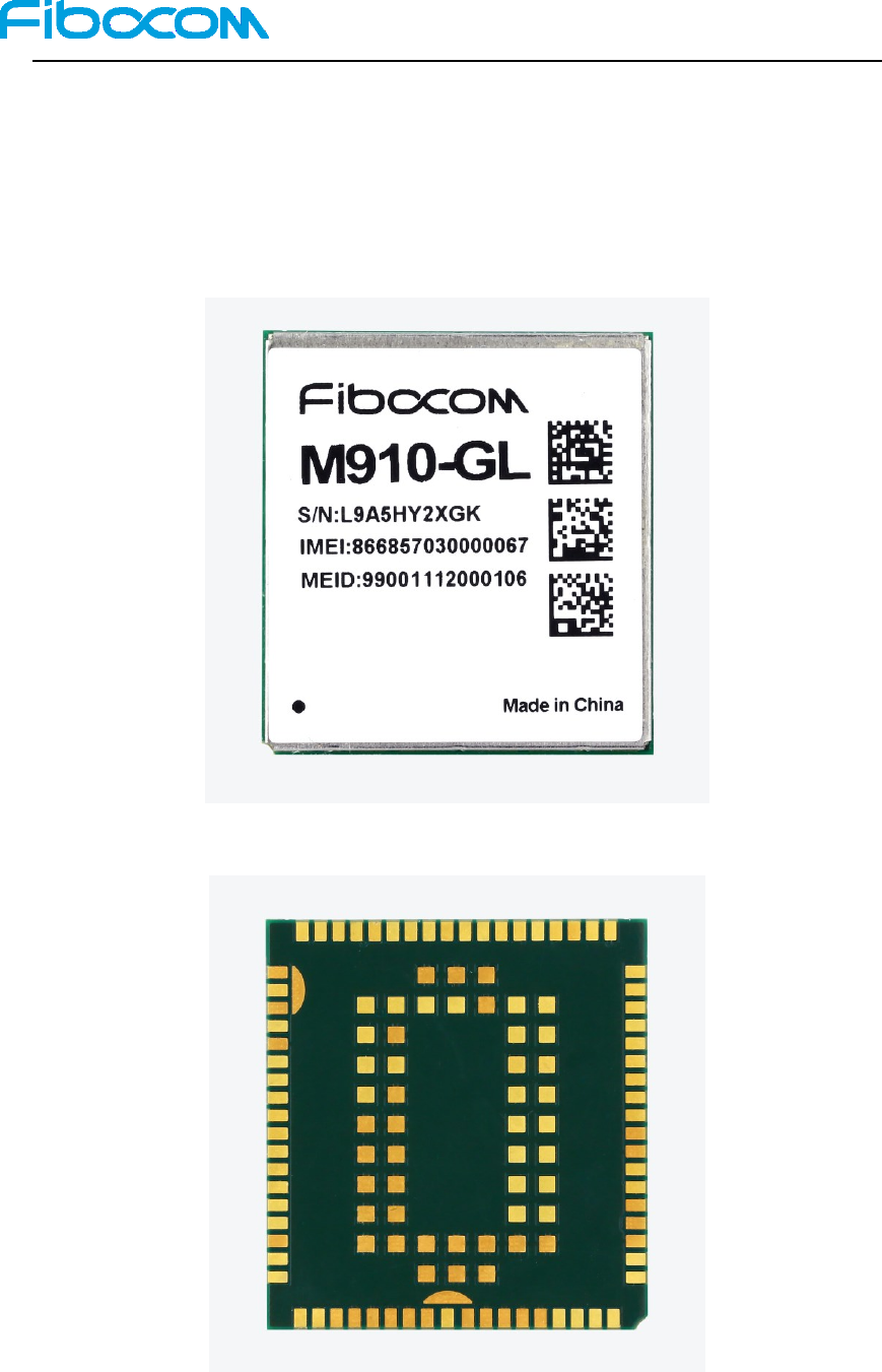
6.1 Product Appearance
The product appearance for M910-GL module is shown in Figure 6-1 and Figure 6-2:
Figure 6-1 Module Product Appearance (Top)
Figure 6-2 Module Product Appearance (Bottom)
Reproduction forbidden without Fibocom Wireless Inc. written authorization - All Rights Reserved.
M910-GL Hardware User Manual Page 42 of 45
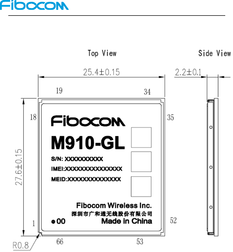
6.2 Dimension of Structure
The structural dimension of the M910-GL module is shown in Figure 6-3:
Figure 6-3 Dimension of Structure (Unit: mm)
6.3 SMT Patch
For module steel net design, please refer to SMT Application Design Instructions for the solder
paste and furnace temperature control.
6.4 Storage
6.4.1 Storage life
M910-GL is shipped in a vacuum-sealed bag. The module storage should follow the following
conditions:

Reproduction forbidden without Fibocom Wireless Inc. written authorization - All Rights Reserved.
M910-GL Hardware User Manual Page 43 of 45
1. If the ambient temperature is below 40°C and the air humidity is less than 90%, the module can
be stored in a vacuum-sealed bag for 12 months.
2. When the vacuum-sealed bag is opened, if the following conditions are met, the module can be
directly re-soldered or go through other high temperature process:
Air humidity for module storage is less than 10%.
The module ambient temperature is below 30°C, air humidity less than 60%, and the factory
completes patch within 168 hours.
6.4.2 Baking
If the module is in the following conditions, it needs to be baked before patching:
1. When the ambient temperature is 23°C (±5°C allowed), the humidity indicator shows that the
humidity is more than 10%.
2. When the vacuum-sealed bag is opened, the module’s ambient temperature is below 30°C, air
humidity is less than 60%, but the factory failed to complete the patch within 168 hours
3. When the vacuum-sealed bag is opened, the air humidity for module storage is more than 10%.
4. If the baking is required, bake the module for 48 hours at 125°C (±5°C allowed).
Note:
The package of the module cannot withstand high temperature baking. Therefore, please
remove the module package before the module is baked.
6.5 Packaging
M910-GL module adopts tray sealed vacuum packaging, combined with the outer packaging
method using the hard carton box, so that the storage, transportation and the usage of modules can
be protected to the greatest extent.
Note:
The vacuum bag contains desiccant. The module is a moisture-sensitive device, with the
moisture sensitive level 3, and it is in line with the standards of the JEDEC. Please avoid
permanent damage to the product caused by moisture.
The module is a precision electronic product, and may suffer permanent damage if no
correct electrostatic protection measures are taken.
Reproduction forbidden without Fibocom Wireless Inc. written authorization - All Rights Reserved.
M910-GL Hardware User Manual Page 44 of 45
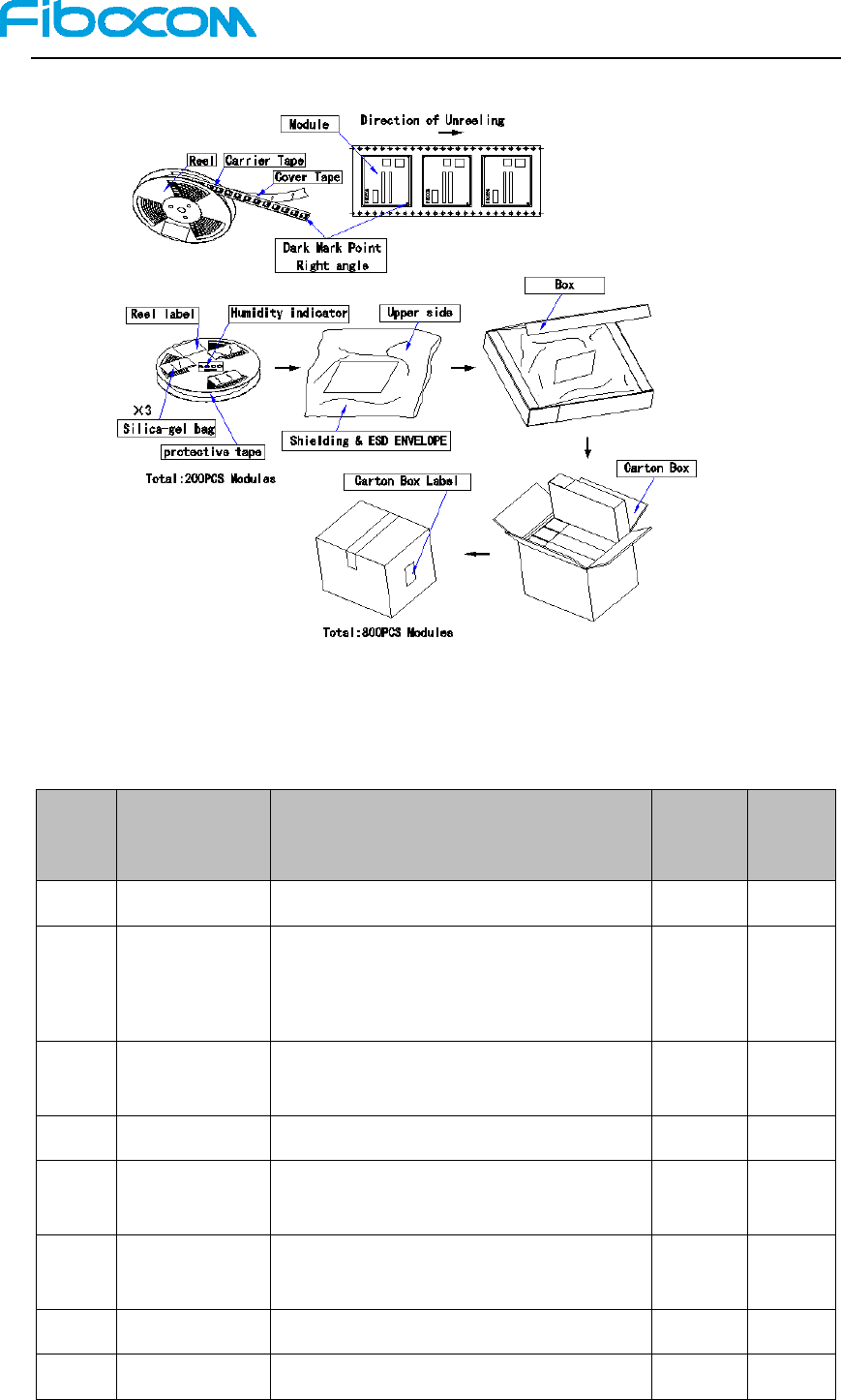
6.5.1 Tape packaging
Figure 6-4 Tape Packaging Flowchart
6.5.2 Packaging list (TBD)
No.
Name
Description
Quantit
y
Confor
m to
RoHS
1
Module
Product module
2
M910-GL_Inne
r box label
Dimension (mm)
1 for each reel, 1 for each antistatic bag, 1
for each inner box
3
M910-GL_Oute
r box label
Dimension (mm), 1 for Outer box
4
Tape
1 for each inner box
5
Reel
Dimension of the reel centering hole must
match with SMT machine feeder area
6
Tape seal sticky
tape
1 for each inner box
7
Humidity card
Four-point humidity card, 1 for each reel
8
Silica desiccant
General silica desiccant, 3 bags per reel

Reproduction forbidden without Fibocom Wireless Inc. written authorization - All Rights Reserved.
M910-GL Hardware User Manual Page 45 of 45
No.
Name
Description
Quantit
y
Confor
m to
RoHS
9
Anti-static bag
Anti-static vacuum bag, with silk anti-static
and moisture-sensitive warning signs
10
Inner box
Dimension: 340×340×75mm
11
Outer box
Dimension 365×330×365mm
12
Sealing label
1 for each inner box, 2 for outer box
13
Sealing tape
_BOPP_transparent