Flaircomm Microelectronics BTM101 Bluetooth module User Manual FLC BTM401 DS
Fujian Flaircomm Microelectronics,Inc. Bluetooth module FLC BTM401 DS
User Manual

FLC-BTM101 Datasheet
Flaircomm Microelectronics Confidential
-1-
FLC-BTM101
Datasheet
Document Type: Bluetooth Module Datasheet
Document Number: FLC-BTM101-DS
Document Version: V1.4
Release Date: 2012/8/29
Copyright 2012 ~ 2014 by Flaircomm Microelectronics Inc., All Right Reserved
Without written permission from Flaircomm Microelectronics Inc., reproduction, transfer, distribution or
storage of part or all of the contents in this document in any form is prohibited
FLC-BTM101 Datasheet
Flaircomm Microelectronics Confidential
-2-
Release Record
Version
Release Date
Comments
1.0
2012/6/26
Initial Release
1.1
2012/8/1
Update Table 2.
1.2
2012/8/6
Add the weight. Add Part 5.1.1 & 5.2 & 5.3. Modify
PCB footprint and reference design.
1.3
2012/8/8
Add BT/CE/FCC logo. Add Cautions & Warnings.
1.4
2012/8/29
Update FCC 2200 logo. Add module statement.

FLC-BTM101 Datasheet
Flaircomm Microelectronics Confidential
-3-
CONTENTS
1. INTRODUCTION .................................................................................................................. 7
1.1 BLOCK DIAGRAM ................................................................................................................... 7
1.2 FEATURES .............................................................................................................................. 7
1.3 APPLICATIONS ....................................................................................................................... 8
2. GENERAL SPECIFICATION ........................................................................................... 10
3. PIN DEFINITION ................................................................................................................ 11
3.1 PIN CONFIGURATION ............................................................................................................ 11
3.2 PIN DEFINITION .................................................................................................................... 11
4. PHYSICAL INTERFACES ................................................................................................ 14
4.1 POWER SUPPLY .................................................................................................................... 14
4.2 RESET .................................................................................................................................. 14
4.2.1 Digital Pin States on Reset ........................................................................................... 14
4.2.2 Power-on Reset ............................................................................................................ 14
4.3 GENERAL PURPOSE DIGITAL IO ........................................................................................... 15
4.4 GENERAL PURPOSE ANALOGUE IO ...................................................................................... 15
5. SERIAL INTERFACES ...................................................................................................... 16
5.1 UART .................................................................................................................................. 16
5.1.1 UART Configuration While in Deep Sleep ................................................................. 16
5.2 I2C INTERFACE ..................................................................................................................... 16
5.3 SPI MASTER INTERFACE ...................................................................................................... 17
5.4 PROGRAMMING AND DEBUG INTERFACE .............................................................................. 18
5.4.1
I
nstruction
Cycle
........................................................................................................... 19
5.4.2
Multi-slave
Operation
.................................................................................................... 19
6. ELECTRICAL CHARACTERISTICS ............................................................................. 21
6.1 ABSOLUTE MAXIMUM RATINGS .......................................................................................... 21
6.2 RECOMMENDED OPERATING CONDITIONS ........................................................................... 21
6.3 INPUT/OUTPUT TERMINAL CHARACTERISTICS ..................................................................... 21
6.3.1 Digital Terminals.......................................................................................................... 21

FLC-BTM101 Datasheet
Flaircomm Microelectronics Confidential
-4-
6.4 AIO ..................................................................................................................................... 22
6.5 POWER CONSUMPTION ......................................................................................................... 22
7. REFERENCE DESIGN ....................................................................................................... 23
8. MECHANICAL CHARACTERISTIC .............................................................................. 24
9. RECOMMENDED REFLOW PROFILE ......................................................................... 27
10. ORDERING INFORMATION ........................................................................................ 29
10.1 PRODUCT PACKAGING INFORMATION ............................................................................... 29
10.2 ORDERING INFORMATION ................................................................................................. 31
10.2.1 Product Revision ....................................................................................................... 31
10.2.2 Shipping Package ...................................................................................................... 31
10.2.3 Product Package ........................................................................................................ 31
10.2.4 Product Grade ........................................................................................................... 32
11. CAUTIONS &WARNINGS ............................................................................................. 33
11.1 FCC STATEMENT .............................................................................................................. 33
11.2 RF WARNING STATEMENT ............................................................................................... 33
11.3 FLC-BTM101 MODULE STATEMENT ............................................................................... 33

FLC-BTM101 Datasheet
Flaircomm Microelectronics Confidential
-5-
TABLES AND FIGURES
Table 1: General Specification ......................................................................................................... 10
Table 2: Pin Definition..................................................................................................................... 13
Table 3: Digital Pin Status on Reset ................................................................................................ 14
Table 4: Power-on Reset .................................................................................................................. 15
Table 5: Possible UART Settings .................................................................................................... 16
Table 6: SPI Master Serial Flash Memory Interface ....................................................................... 17
Table 7: Instruction Cycle for a SPI Transaction............................................................................. 19
Table 8: Absolute Maximum Ratings .............................................................................................. 21
Table 9: Recommended Operating Conditions ................................................................................ 21
Table 10: Digital Terminal............................................................................................................... 22
Table 11: Power Consumption......................................................................................................... 22
Table 12: Product Revision .............................................................................................................. 31
Table 13: Shipping Package............................................................................................................. 31
Table 14: Product Package ............................................................................................................... 31
Table 15: Product Grade .................................................................................................................. 32
Figure 1: Block Diagram ................................................................................................................... 7
Figure 2: Pin Configuration ............................................................................................................. 11
Figure 3: Example of an I2C Interface EEPROM Connection ........................................................ 17
Figure 4: Memory Boot-up Sequence .............................................................................................. 18
Figure 5: Reference Design ............................................................................................................. 23
Figure 6: Top View .......................................................................................................................... 24
Figure 7: Bottom View .................................................................................................................... 24
Figure 8: Detail of Pads ................................................................................................................... 25
Figure 9: Recommended PCB Footprint.......................................................................................... 26
Figure 10: Recommended Reflow Profile ....................................................................................... 27
Figure 11: Product Packaging Information ...................................................................................... 29

FLC-BTM101 Datasheet
Flaircomm Microelectronics Confidential
-6-
Figure 12: Product Packaging Information (Tape) .......................................................................... 31
Figure 13: Ordering Information ..................................................................................................... 31
FLC-BTM101 Datasheet
Flaircomm Microelectronics Confidential
-7-
1. Introduction
FLC-BTM101 is a Bluetooth low energy (BLE) module supporting BT4.0 (BLE only). This module
enables customers to add ultra-low power wireless connectivity to their products. The module
provides everything required to create a Bluetooth low energy product with RF, based band, MCU,
system clock, antenna and qualified Bluetooth 4.0 (BLE only) stack and customer application
settings. It also enables the transfer of short data sets between compact devices opening up a
completely new area of Bluetooth applications such as watches, TV remote controls, medical sensors
and fitness trainers.
Bluetooth low energy takes less time to establish a connection than conventional Bluetooth wireless
technology and can consume approximately 1/20th of the power of Bluetooth Basic Rate. BTM101
support profiles for sensors, watches, HIDs and time synchronization. Naming Declaration
1.1 Block Diagram
UART
PIOs
FLC-BTM101
PM Two
Clocks
CSR1000 BLE
Filter
SPI
VDD
Antenna
Figure 1: Block Diagram
1.2 Features
Bluetooth v4.0(BLE only)( doesn’t support BT2.0& BT 2.1 &BT3.0)

FLC-BTM101 Datasheet
Flaircomm Microelectronics Confidential
-8-
Support of Bluetooth 4.0(BLE only) specification host stack including ATT, GATT, SMP,
L2CAP, GAP
RSSI monitoring for proximity applications
32kHz and 16MHz system clocks
10 bits ADC
12 digital PIOs
3 analog AIOs
UART host interface
512 Kbits EEPROM
Debug SPI host interface
3 PWM modules
Wakeup interrupt
64KB RAM and 64K ROM
Watchdog timer
Small form factor
SMT pads for easy and reliable PCB mounting
BQB/FCC/CE Certified
RoHS compliant
1.3 Applications
Typical applications are:
Sports and fitness
Healthcare
Home automation
Office and mobile accessories
Automotive

FLC-BTM101 Datasheet
Flaircomm Microelectronics Confidential
-9-
Commercial
Watches
Human interface devices
FLC-BTM101 Datasheet
Flaircomm Microelectronics Confidential
-10-
2. General Specification
Bluetooth Specification
Standard
Bluetooth 4.0(BLE only)
Frequency Band
2.402GHz ~ 2.480GHz
Antenna
Antenna
High System Clock
16MHz
Low System Clock
32.768kHz
Interface
UART, PIO, SPI, AIO
Sensitivity
-90dBm@0.1%BER
RF TX Power
6dBm
Power
Supply Voltage
1.8 ~ 3.6V DC
Operational Current
Refer to Table 11
Deep Sleep Current
<5uA in deep sleep mode
Operating Environment
Temperature
-30ºC to +85ºC
Certifications
BQB/FCC /CE2200
Environmental
RoHS Compliant
Dimension and Weight
Dimension
22.00mm x 13.40mm x 1.50mm
Weight
1.08g
Table 1: General Specification
FLC-BTM101 Datasheet
Flaircomm Microelectronics Confidential
-11-
3. Pin Definition
3.1 Pin Configuration
Figure 2: Pin Configuration
3.2 Pin Definition
Pin
Symbol
I/O Type
Description
1
GND
Ground
Ground
2
AIO2
Bidirectional analogue
Analogue programmable I/O line
3
AIO1
Bidirectional analogue
Analogue programmable I/O line
4
AIO0
Bidirectional analogue
Analogue programmable I/O line

FLC-BTM101 Datasheet
Flaircomm Microelectronics Confidential
-12-
5
PIO0 /
UART_TX
Bi-directional with
programmable strength internal
pull-up/down
Programmable input/output line / UART TX
selected by firmware setting
6
PIO1 /
UART_RX
Bi-directional with
programmable strength internal
pull-up/down
Programmable input/output line / UART RX
selected by firmware setting
7
PIO3
Bi-directional with
programmable strength internal
pull-up/down
Programmable input/output line
8
PIO4
Bi-directional with
programmable strength internal
pull-up/down
Programmable input/output line
9
PIO5 /
SPI_CLK
Bi-directional with
programmable strength internal
pull-up/down
Programmable input/output line / SPI Clock
selected by SPI_PIO#
10
GND
Ground
Ground
11
PIO6 /
SPI_CSB
Bi-directional with
programmable strength internal
pull-up/down
Programmable input/output line / SPI CSB
selected by SPI_PIO#
12
PIO7 /
SPI_MOSI
Bi-directional with
programmable strength internal
pull-up/down
Programmable input/output line / SPI MOSI
selected by SPI_PIO#
13
PIO8 /
SPI_MISO
Bi-directional with
programmable strength internal
pull-up/down
Programmable input/output line / SPI MISO
selected by SPI_PIO#
14
PIO9
Bi-directional with
programmable strength internal
pull-up/down
Programmable input/output line
15
I2C_SDA
Bidirectional, tristate, with
weak internal pull-up
I2C data input/output
16
I2C_SCL
Input with weak internal pull-up
I2C clock
17
GND
Ground
Ground
18
PIO2
Bi-directional with
programmable strength internal
pull-up/down
Programmable input/output line

FLC-BTM101 Datasheet
Flaircomm Microelectronics Confidential
-13-
19
PIO10
Bi-directional with
programmable strength internal
pull-up/down
Programmable input/output line
20
VDD_PIO
Power Input
Positive supply for all digital I/O port PIO[11:0]
21
PIO11
Bi-directional with
programmable strength internal
pull-up/down
Programmable input/output line
22
SPI_PIO#SEL
Input with strong internal pull-
down
Select SPI debug port on PIO[8:5]
23
Wake-up
Input has no internal pull-up or
pull-down, use external pull-
down
Input to wake up BTM101 from hibernate
24
VDD
Power input
3.3v power input
25
GND
Ground
Ground
26
GND
Ground
Ground
Table 2: Pin Definition
FLC-BTM101 Datasheet
Flaircomm Microelectronics Confidential
-14-
4. Physical Interfaces
4.1 Power Supply
BTM101 contains two regulators:
One switch-mode regulator, which generates the main supply rail directly from battery
One low-voltage linear regulator with 1.2V output powers digital circuits
VDD_PIO is input voltage to power all digital I/Os including PIOs, UART port, SPI port and I2C.
4.2 Reset
The module may be reset from several sources:
Power-on reset
Software configured watchdog timer.
4.2.1 Digital Pin States on Reset
The following table shows the digital pin states of BTM101 on reset. PU and PD default to weak
values unless specified otherwise.
Pin
Name
/
Group
On
Reset
I2C_SDA
Strong
PU
I2C_SCL
Strong
PU
PIO[11:0]
Weak
PD
Table 3: Digital Pin Status on Reset
4.2.2 Power-on Reset
The following table shows how the power-on reset occurs.

FLC-BTM101 Datasheet
Flaircomm Microelectronics Confidential
-15-
Power-on
Reset
Type
Unit
Reset
release
on
VDD_DIG
rising
1.05
V
Reset
assert
on
VDD_DIG
falling
1.00
Reset
assert
on
VDD_DIG
falling
(Sleep
mode)
0.60
Hysteresis
50
mV
Table 4: Power-on Reset
4.3 General Purpose Digital IO
12 lines of programmable bidirectional I/O are provided. They are all powered from VDD_PIO.
PIO lines are software configurable as weak pull-up, weak pull-down, strong pull-up or strong pull-
down.
NOTE: at reset all PIO lines are input with weak pull-downs.
Any of the PIO line can be configured as interrupt request line or as weak-up lines from sleep modes.
The BTM101 supports alternative functions on the PIO lines:
SPI interface,
UART.
LED flashing / PWM module.
NOTE: Implementation of the PIO lines is firmware build specific.
4.4 General Purpose Analogue IO
BTM101 has 3 general purpose analog interface pins, AIO [2:0].
FLC-BTM101 Datasheet
Flaircomm Microelectronics Confidential
-16-
5. Serial Interfaces
5.1 UART
This is a standard UART interface for communicating with other serial devices. The UART interface
provides a simple mechanism for communicating with other serial devices using the RS232 protocol.
When the module is connected to another digital device, UART_RX and UART_TX transfer data
between the two devices.
When selected in firmware PIO[0] is assigned to UART_TX and PIO[1] is assigned to UART_RX.
The UART CTS and RTS signals can be assigned to any PIO pin by the on-chip firmware.
Parameter
Possible Values
Baud Rate
Minimum
1200 baud (≤2%Error)
9600 baud (≤1%Error)
Maximum
4M baud (≤1%Error)
Flow control
CTS / RTS
Parity
None, Odd or Even
Number of Stop Bits
1 or 2
Bits per Byte
8
Table 5: Possible UART Settings
5.1.1 UART Configuration While in Deep Sleep
The maximum baud rate is 9600 baud during deep sleep.
5.2 I2C Interface
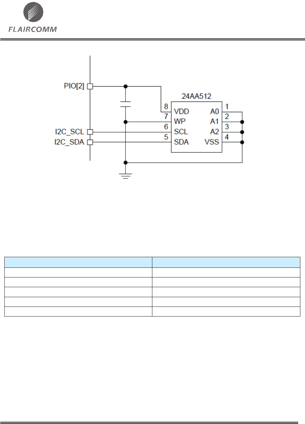
The I2C interface communicates to an internal EEPROM, or external peripherals or sensors. The
internal EEPROM holds the program code inside BTM101.
Figure 3 shows the connection of the internal EEPROM with the I2C interface where I2C_SCL,
I2C_SDA and PIO [2] are connected to the internal EEPROM. The PIO [2] pin supplies the power to
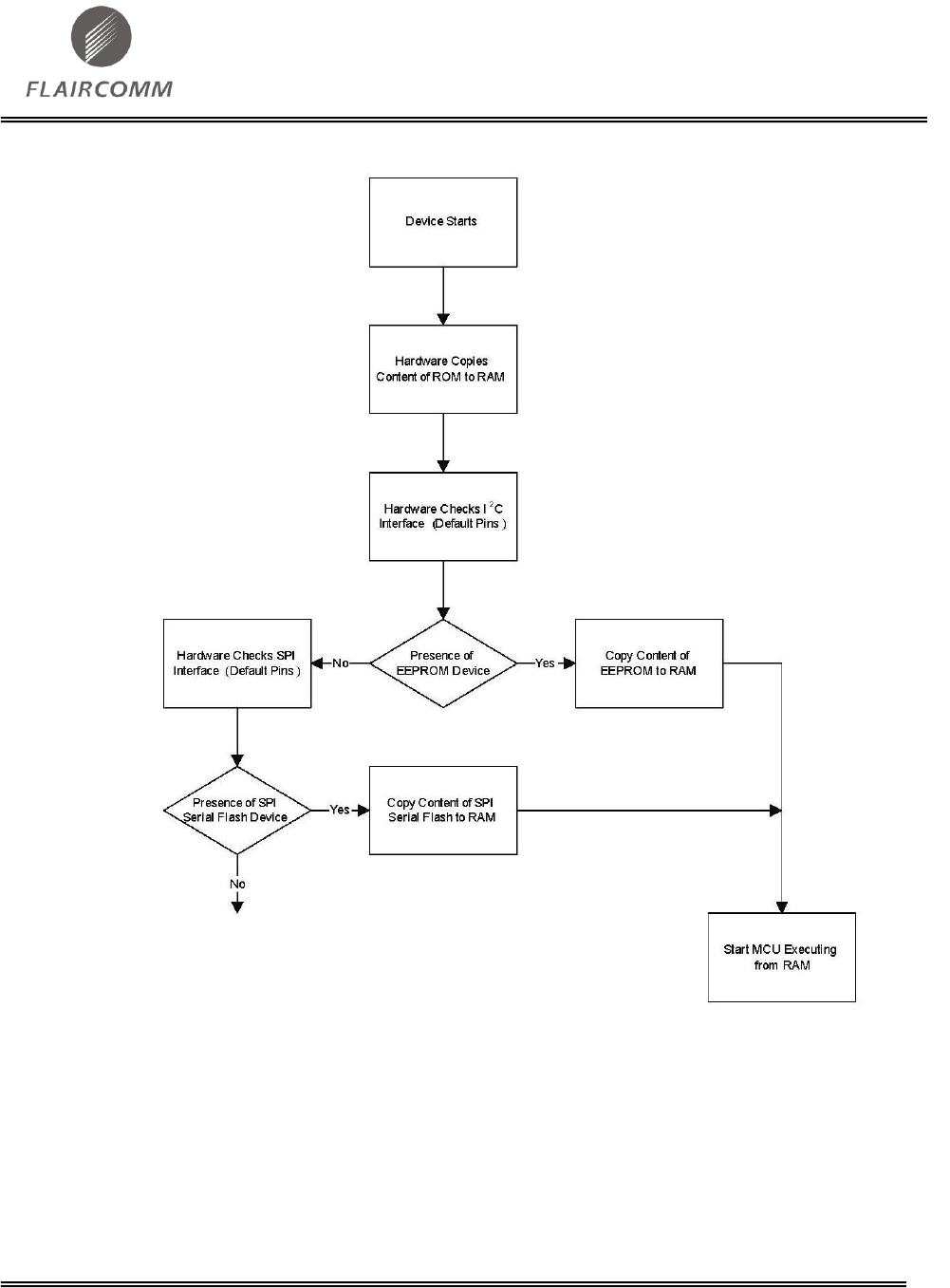
the EEPROM supply pin, e.g. VDD. At boot-up, if there is no valid ROM image in the BTM101
ROM area, BTM101 tries to boot from the I2C interface, see Figure 4. This involves reading the
code from the internal EEPROM and loading it into the internal BTM101 RAM.
FLC-BTM101 Datasheet
Flaircomm Microelectronics Confidential
-17-
Figure 3: Example of an I2C Interface EEPROM Connection
5.3 SPI Master Interface
BTM101 provides a SPI interface to connect an external serial flash memory. The SPI master
memory interface in the BTM101 is overlaid on the I2C interface and uses a further 3 PIOs for the
extra pins, see Table 6.
SPI Interface
Pin
Flash_VDD
PIO[2]
SF_DIN
PIO[3]
SF_CS#
PIO[4]
SF_CLK
I2C_SCL
SF_DOUT
I2C_SDA
Table 6: SPI Master Serial Flash Memory Interface
Note:
If an application using BTM101 is designed to boot from SPI serial flash, it is possible for the
firmware to map the I2C interface to alternative PIOs.
The boot-up sequence for BTM101 is controlled by hardware and firmware. Figure 4 shows the
sequence of loading RAM with content from RAM, EEPROM and SPI serial flash.
FLC-BTM101 Datasheet
Flaircomm Microelectronics Confidential
-18-
Figure 4: Memory Boot-up Sequence
5.4 Programming and Debug Interface
The BTM101 debug SPI interface is available in SPI slave mode to enable an external MCU to
program and control the BTM101, generally via libraries or tools supplied by Flaircomm. The

FLC-BTM101 Datasheet
Flaircomm Microelectronics Confidential
-19-
protocol of this interface is proprietary. The 4 SPI debug lines directly support this function. The
SPI programs, configures and debugs the BTM101.
Take SPI_PIO#_SEL high to enable the SPI debug feature on PIO [8:5].
BTM101 uses a 16-bit data and 16-bit address programming and debug interface. Transactions occur
when the internal processor is running or is stopped.
Data is written or read one word at a time, or the auto-increment feature is available for block access.
5.4.1
I
nstruction
Cycle
The BTM101 is the slave and receives commands on DEBUG_MOSI and outputs data on
DEBUG_MISO. Table 7 shows the instruction cycle for a SPI transaction.
1
Reset the SPI interface
Hold DEBUG_CS# high for 2 DEBUG_CLK cycles
2
Write the command word
Take DEBUG_CS# low and clock in the 8-bit
command
3
Write the address
Clock in the 16-bit address word
4
Write or read data words
Clock in or out 16-bit data word(s)
5
Termination
Take DEBUG_CS# high
Table 7: Instruction Cycle for a SPI Transaction
With the exception of reset, DEBUG_CS# must be held low during the transaction. Data on
DEBUG_MOSI is clocked into the BTM101 on the rising edge of the clock line DEBUG_CLK.
When reading, BTM101 replies to the master on DEBUG_MISO with the data changing on the
falling edge of the DEBUG_CLK. The master provides the clock on DEBUG_CLK. The transaction
is terminated by taking DEBUG_CS# high.
The auto increment operation on the BTM101 cuts down on the overhead of sending a command
word and the address of a register for each read or write, especially when large amounts of data are
to be transferred. The auto increment offers increased data transfer efficiency on the BTM101. To
invoke auto increment, DEBUG_CS# is kept low, which auto increments the address, while
providing an extra 16 clock cycles for each extra word written or read.
5.4.2
M
ulti-slave
Operation

FLC-BTM101 Datasheet
Flaircomm Microelectronics Confidential
-20-
Do not connect the BTM101 in a multi-slave arrangement by simple parallel connection of slave
MISO lines. When BTM101 is deselected (DEBUG_CS# = 1), the DEBUG_MISO line does not
float. Instead,
BTM101 outputs 0 if the processor is running or 1 if it is stopped.
FLC-BTM101 Datasheet
Flaircomm Microelectronics Confidential
-21-
6. Electrical Characteristics
6.1 Absolute Maximum Ratings
Rating
Min
Max
Unit
Storage Temperature
-40
+85
°C
Operating Temperature
-40
+85
°C
PIO Voltage
-0.4
+3.6
V
Battery (VDD) operation
1.8
+3.6
V
Other Voltages
VSS-0.4
VDD+0.4
V
Table 8: Absolute Maximum Ratings
6.2 Recommended Operating Conditions
Operating Condition
Min
Typical
Max
Unit
Storage Temperature
-40
--
+85
°C
Operating Temperature Range
-30
--
+85
°C
PIO Voltage
+1.2
--
+3.6
V
VDD Voltage
+1.8
--
+3.6
V
Table 9: Recommended Operating Conditions
6.3 Input/output Terminal Characteristics
6.3.1 Digital Terminals
Supply Voltage Levels
Min
Typical
Max
Unit
Input Voltage Levels
VIL input logic level low
-0.4
-
+0.4
V
VIH input logic level high
0.7VDD
-
VDD+0.4
V
Tr/Tf
-
-
25
ns
Output Voltage Levels
VOL output logic level low, lOL = 4.0mA
-
-
0.4
V
VOH output logic level high, lOH = -4.0mA
0.75VDD
-
-
V
FLC-BTM101 Datasheet
Flaircomm Microelectronics Confidential
-22-
Tr/Tf
-
-
5
ns
Input and Tri-state Current
With strong pull-up
-150
-40
-10
μA
With strong pull-down
10
40
150
μA
With weak pull-up
-5
-1.0
-0.33
μA
With weak pull-down
-0.33
+1.0
5.0
μA
I/O pad leakage current
-1
0
+1
μA
CI Input Capacitance
1.0
-
5.0
pF
Table 10: Digital Terminal
6.4 AIO
Input Voltage Levels
Min
Typical
Max
Unit
Input Voltages
0
--
+1.3
V
6.5 Power Consumption
Operation Mode
Description
Typical
Unit
Dormant
All functions are shutdown. To wake up toggle the
WAKE pin
<600
nA
Hibernate
VDD_PIO = ON. REFCLK = OFF, SLEEPCLK=ON,
VDD=ON
<1.5
uA
Deep Sleep
VDD_PIO=ON, REFCLK=OFF,
SLEEPCLK=ON,VDD=ON,RAM=ON,DIGITAL
CIRCUITS=ON, SMPS=ON (low-power mode), 1us
wake up time
<5
uA
Idle
VDD_PIO=ON, REFCLK=ON,
SLEEPCLK=ON,VDD=ON,RAM=ON,DIGITAL
CIRCUITS=ON, MCU=IDLE, <1us wake up time
~1
mA
RX / TX active
@3V peak
~16
mA
Table 11: Power Consumption
FLC-BTM101 Datasheet
Flaircomm Microelectronics Confidential
-23-
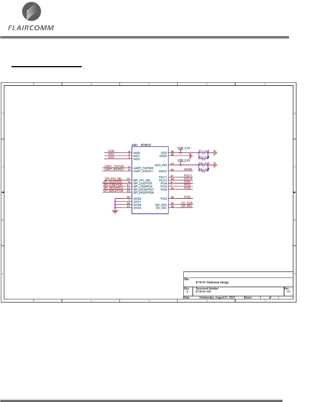
7. Reference Design
Figure 5: Reference Design
FLC-BTM101 Datasheet
Flaircomm Microelectronics Confidential
-24-
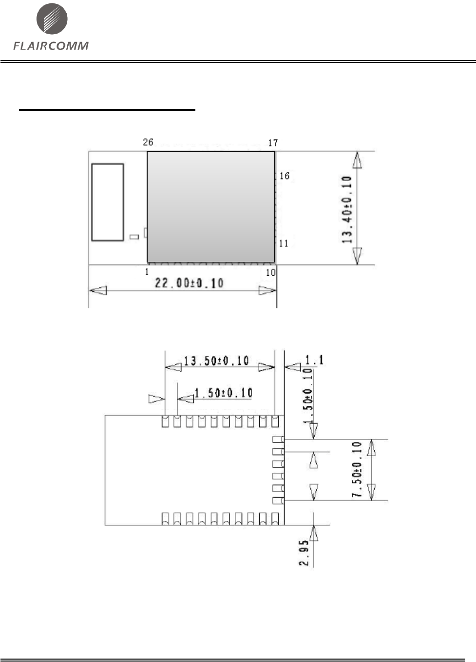
8. Mechanical Characteristic
Figure 6: Top View
Figure 7: Bottom View
FLC-BTM101 Datasheet
Flaircomm Microelectronics Confidential
-25-
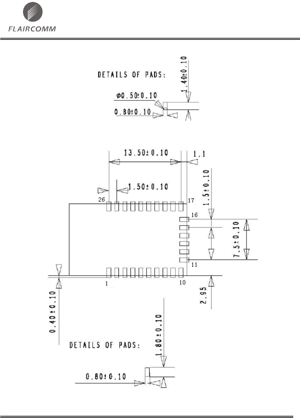
Figure 8: Detail of Pads

FLC-BTM101 Datasheet
Flaircomm Microelectronics Confidential
-26-
Figure 9: Recommended PCB Footprint
FLC-BTM101 Datasheet
Flaircomm Microelectronics Confidential
-27-
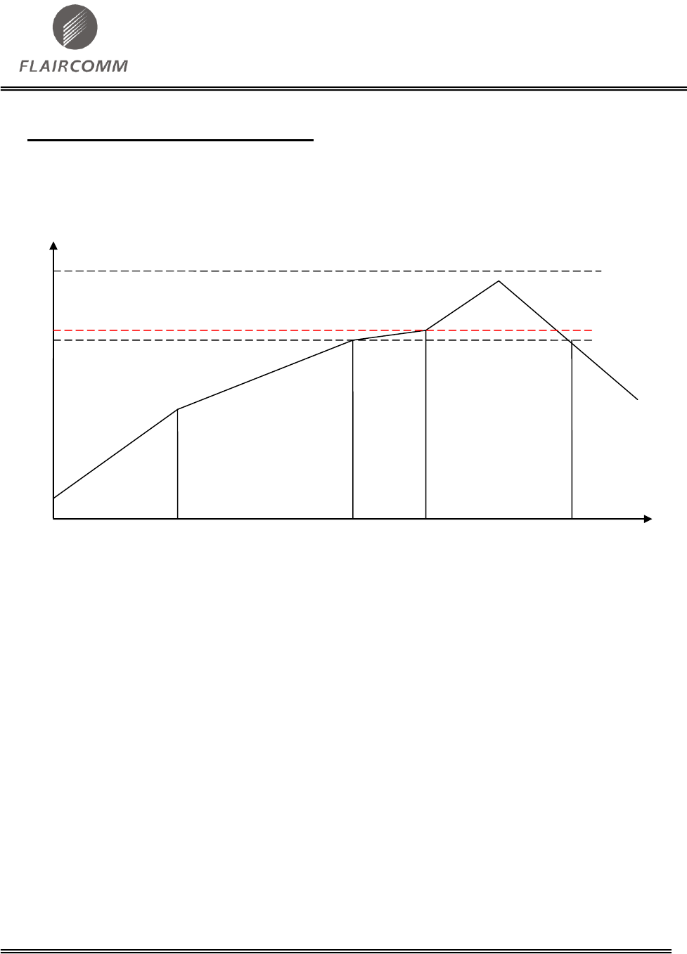
9. Recommended Reflow Profile
The soldering profile depends on various parameters necessitating a set up for each application. The
data here is given only for guidance on solder reflow.
210
217
℃
250
A
B
C
D
1
2
0
25
3
4
5
6
min
E
Figure 10: Recommended Reflow Profile
Pre-heat zone (A) — This zone raises the temperature at a controlled rate, typically 0.5 – 2 C/s.
The purpose of this zone is to preheat the PCB board and components to 120 ~ 150 C. This stage is
required to distribute the heat uniformly to the PCB board and completely remove solvent to reduce
the heat shock to components.
Equilibrium Zone 1 (B) — In this stage the flux becomes soft and uniformly encapsulates solder
particles and spread over PCB board, preventing them from being re-oxidized. Also with elevation
of temperature and liquefaction of flux, each activator and rosin get activated and start eliminating
oxide film formed on the surface of each solder particle and PCB board. The temperature is
recommended to be 150 to 210 for 60 to 120 second for this zone.
Equilibrium Zone 2 (c) (optional) — In order to resolve the upright component issue, it is
recommended to keep the temperature in 210 – 217 for about 20 to 30 second.
Reflow Zone (D) — The profile in the figure is designed for Sn/Ag3.0/Cu0.5. It can be a reference
for other lead-free solder. The peak temperature should be high enough to achieve good wetting but
not so high as to cause component discoloration or damage. Excessive soldering time can lead to

FLC-BTM101 Datasheet
Flaircomm Microelectronics Confidential
-28-
intermetallic growth which can result in a brittle joint. The recommended peak temperature (Tp) is
230 ~ 250 C. The soldering time should be 30 to 90 second when the temperature is above 217 C.
Cooling Zone (E) — The cooling ate should be fast, to keep the solder grains small which will give
a longerlasting joint. Typical cooling rate should be 4 C.
FLC-BTM101 Datasheet
Flaircomm Microelectronics Confidential
-29-
10. Ordering Information
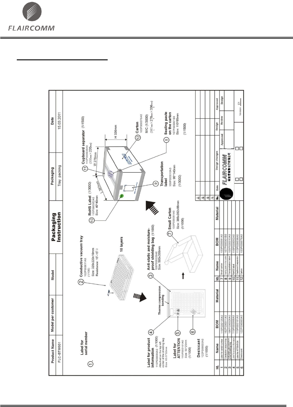
10.1 Product Packaging Information
Figure 11: Product Packaging Information
FLC-BTM101 Datasheet
Flaircomm Microelectronics Confidential
-30-
FLC-BTM101 Datasheet
Flaircomm Microelectronics Confidential
-31-
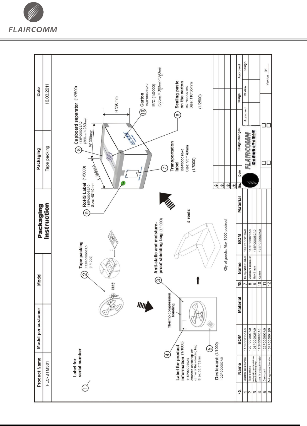
Figure 12: Product Packaging Information (Tape)
10.2 Ordering information
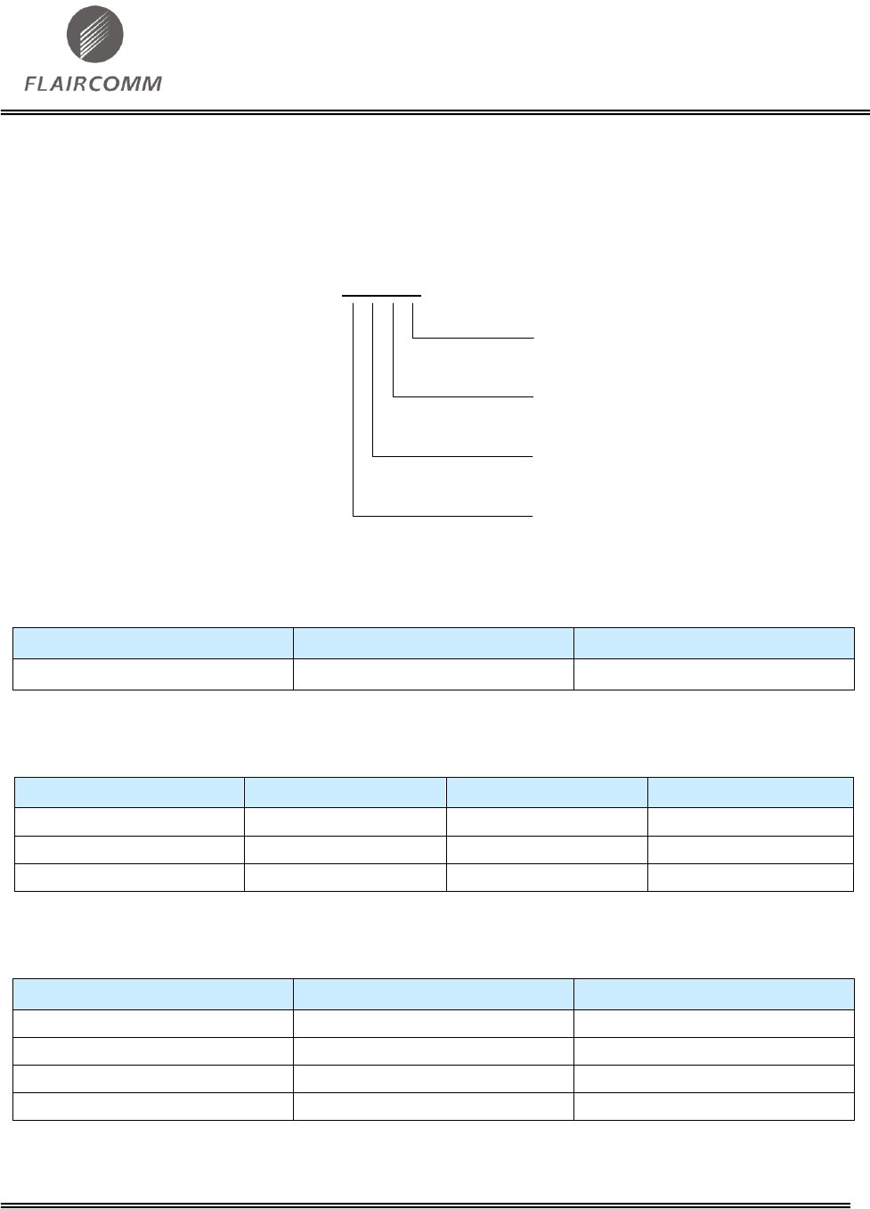
FLC-BTM101XYZA
Product Revision
Shipping Package
Product Package
Product Grade
Figure 13: Ordering Information
10.2.1 Product Revision
Product Revision
Description
Availability
A
Release A
Yes
Table 12: Product Revision
10.2.2 Shipping Package
Shipping Package
Description
Quantity
Availability
0
Foam Tray
—
No
1
Plastic Tray
100x10x3 = 3000
Yes
2
Tape
1000
Yes
Table 13: Shipping Package
10.2.3 Product Package
Product Package
Description
Availability
Q
QFN
Yes
L
LGA
No
B
BGA
No
C
Connector
No
Table 14: Product Package
FLC-BTM101 Datasheet
Flaircomm Microelectronics Confidential
-32-
10.2.4 Product Grade
Product Grade
Description
Availability
C
Consumer
Yes
I
Industrial
No
V
Automobile After-Market
Yes
A
Automobile Before-Market
No
Table 15: Product Grade

FLC-BTM101 Datasheet
Flaircomm Microelectronics Confidential
-33-
11. Cautions &Warnings
11.1 FCC Statement
1. This device complies with Part 15 of the FCC Rules. Operation is subject to the following two
conditions:
(1) This device may not cause harmful interference.
(2) This device must accept any interference received, including interference that may cause
undesired operation.
2. Changes or modifications not expressly approved by the party responsible for compliance could
void the user's authority to operate the equipment.
NOTE: This equipment has been tested and found to comply with the limits for a Class B digital
device, pursuant to Part 15 of the FCC Rules. These limits are designed to provide reasonable
protection against harmful interference in a residential installation.
This equipment generates uses and can radiate radio frequency energy and, if not installed and used
in accordance with the instructions, may cause harmful interference to radio communications.
However, there is no guarantee that interference will not occur in a particular installation. If this
equipment does cause harmful interference to radio or television reception, which can be determined
by turning the equipment off and on, the user is encouraged to try to correct the interference by one
or more of the following measures:
Reorient or relocate the receiving antenna.
Increase the separation between the equipment and receiver.
Connect the equipment into an outlet on a circuit different from that to which the receiver is
connected.
Consult the dealer or an experienced radio/TV technician for help.
11.2 RF Warning Statement
The device has been evaluated to meet general RF exposure requirement. The device can be used in
portable exposure condition without restriction.
11.3 FLC-BTM101 Module Statement
The FLC-BTM101 module is designed to comply with the FCC statements.

FLC-BTM101 Datasheet
Flaircomm Microelectronics Confidential
-34-
The Host system using BTM101, should have label indicated "Contains FCC ID: P4IBTM101."