Flaircomm Microelectronics WFM301 WIFI Module User Manual FLC BTM401 DS
Fujian Flaircomm Microelectronics,Inc. WIFI Module FLC BTM401 DS
User Manual
FLC-WFM301 Datasheet
Flaircomm Microelectronics Confidential
-1-
FLC-WFM301
Datasheet
Document Type: WiFi Module Datasheet
Document Number: FLC-WFM301-DS
Document Version: V1.3
Release Date: 2012/12/07
Copyright 2012 ~ 2014 by Flaircomm Microelectronics Inc., All Right Reserved
Without written permission from Flaircomm Microelectronics Inc., reproduction, transfer, distribution or
storage of part or all of the contents in this document in any form is prohibited

FLC-WFM301 Datasheet
Flaircomm Microelectronics Confidential
-2-
Release Record
Version
Release Date
Comments
1.0
2012/6/26
Release
1.1
2012/9/25
Add CE/FCC logo. Add Cautions & Warnings.
Reformat the text.
1.2
2012/11/13
Modify 11.3 Label Instructions.
1.3
2012/12/07
Modify Frequency Band and FCC Radiation
Exposure Statement. Add Antenna Specifications.

FLC-WFM301 Datasheet
Flaircomm Microelectronics Confidential
-3-
CONTENTS
1. INTRODUCTION .................................................................................................................................................. 6
1.1 BLOCK DIAGRAM .................................................................................................................................................. 6
1.2 FEATURES ............................................................................................................................................................. 6
1.3 FUNCTIONS ........................................................................................................................................................... 7
1.4 APPLICATIONS ...................................................................................................................................................... 8
2. GENERAL SPECIFICATION ............................................................................................................................. 9
3. PIN DEFINITION ................................................................................................................................................ 10
3.1 PIN CONFIGURATION ........................................................................................................................................... 10
3.2 PIN DEFINITION ................................................................................................................................................... 10
4. PHYSICAL INTERFACES ................................................................................................................................ 13
4.1 POWER SUPPLY ................................................................................................................................................... 13
4.1.1 Linear Regulators ....................................................................................................................................... 13
4.1.2 LDO for Digital Supply .............................................................................................................................. 13
4.1.3 RF Front End Power Supply ...................................................................................................................... 13
4.1.4 I/O Power Supply ....................................................................................................................................... 13
4.2 RESET ................................................................................................................................................................. 13
4.3 RF INTERFACE .................................................................................................................................................... 14
4.4 GENERAL PURPOSE DIGITAL IO .......................................................................................................................... 14
4.5 ANALOG IO ......................................................................................................................................................... 14
4.6 HOST INTERFACES .............................................................................................................................................. 14
4.6.1 SDIO .......................................................................................................................................................... 15
5. ELECTRICAL CHARACTERISTIC ................................................................................................................ 17
5.1 WIFI PERFORMANCE SPECIFICATIONS ................................................................................................................ 17
5.1.1 DSSS and CCK modulations (802.11b) TX Performance Specifications .................................................. 17
5.1.2 OFDM TX Performance Specifications ..................................................................................................... 17
5.1.3 DSSS and CCK modulations (802.11b) RX Performance Specifications .................................................. 17
5.1.4 OFDM RX Performance Specifications ..................................................................................................... 17
5.2 DC ELECTRICAL SPECIFICATIONS ....................................................................................................................... 18
5.2.1 Absolute Maximum Ratings ....................................................................................................................... 18
5.2.2 Recommended Operating Conditions ......................................................................................................... 18
5.2.3 Current Consumption ................................................................................................................................. 19
5.2.4 Digital Characteristics ................................................................................................................................ 19
5.2.5 Clock Characteristics .................................................................................................................................. 19
5.2.6 Power-on Reset Characteristics .................................................................................................................. 19
6. REFERENCE DESIGN ....................................................................................................................................... 21
7. MECHANICAL CHARACTERISTIC .............................................................................................................. 22
8. RECOMMENDED PCB LAYOUT AND MOUNTING PATTERN............................................................... 23
8.1 ANTENNA CONNECTION AND GROUNDING PLANE DESIGN ................................................................................. 23
9. RECOMMENDED REFLOW PROFILE ......................................................................................................... 25
10. ORDERING INFORMATION ....................................................................................................................... 26
10.1 PRODUCT PACKAGING INFORMATION ................................................................................................................. 26
10.2 ORDERING INFORMATION .................................................................................................................................... 26
10.2.1 Product Revision ........................................................................................................................................ 26
10.2.2 Shipping Package ....................................................................................................................................... 26
10.2.3 Product Package ......................................................................................................................................... 26

FLC-WFM301 Datasheet
Flaircomm Microelectronics Confidential
-4-
10.2.4 Product Grade ............................................................................................................................................. 27
11. CAUTIONS &WARNINGS ............................................................................................................................ 28
11.1 FCC STATEMENT ................................................................................................................................................ 28
11.2 FCC RADIATION EXPOSURE STATEMENT ........................................................................................................... 28
11.3 FLC-WFM301 LABEL INSTRUCTIONS ................................................................................................................ 28
11.4 FLC-BTM301 ANTENNA STATEMENT ................................................................................................................ 29
11.4.1 Antenna Electrical Specifications............................................................................................................... 29
11.4.2 Radiation Gain and Pattern ......................................................................................................................... 29

FLC-WFM301 Datasheet
Flaircomm Microelectronics Confidential
-5-
TABLES AND FIGURES
Table 1: General Specification ......................................................................................................................................... 9
Table 2: Pin Definition ................................................................................................................................................... 12
Table 3: GPIO Usage ..................................................................................................................................................... 14
Table 4: Analog IO Usage .............................................................................................................................................. 14
Table 5: Analog IO Usage .............................................................................................................................................. 15
Table 6: DSSS and CCK modulations (802.11b) TX Performance Specifications ........................................................ 17
Table 7: OFDM TX Performance Specifications ........................................................................................................... 17
Table 8: OFDM TX Performance Specifications ........................................................................................................... 17
Table 9: OFDM RX Performance Specifications ........................................................................................................... 18
Table 10: Absolute Maximum Ratings .......................................................................................................................... 18
Table 11: Recommended Operating Conditions ............................................................................................................ 19
Table 12: Current Consumption ..................................................................................................................................... 19
Table 13: Digital Characteristics .................................................................................................................................... 19
Table 14: Clock Characteristics ..................................................................................................................................... 19
Table 15: Power-on Reset Characteristics ...................................................................................................................... 20
Table 16: Product Revision ............................................................................................................................................ 26
Table 17: Shipping Package ........................................................................................................................................... 26
Table 18: Product Package ............................................................................................................................................. 27
Table 19: Product Grade ................................................................................................................................................ 27
Table 20: Antenna Electrical Specifications .................................................................................................................. 29
Table 20: Radiation Gain and Pattern ............................................................................................................................ 29
Figure 1: Block Diagram .................................................................................................................................................. 6
Figure 2: Pin Configuration............................................................................................................................................ 10
Figure 3: Reference Design ............................................................................................................................................ 21
Figure 4: Mechanical Characteristic............................................................................................................................... 22
Figure 5: Pad Size .......................................................................................................................................................... 22
Figure 6: Placement the Module on a System Board ..................................................................................................... 23
Figure 7: Leave 5mm Clearance Space from the Antenna ............................................................................................. 23
Figure 8: Recommended Trace Connects Antenna and the Module .............................................................................. 24
Figure 9: Recommended Reflow Profile ........................................................................................................................ 25
Figure 10: Product Packaging Information .................................................................................................................... 26
Figure 11: Ordering Information .................................................................................................................................... 26
Figure 12: ALA931C5 Radiation Pattern : Azimuth@2.45GHz .................................................................................... 30
Figure 13: ALA931C5 Radiation Pattern : Elevation1@2.45GHz ............................................................................... 31
Figure 14: ALA931C5 Radiation Pattern : Elevation2@2.45GHz ............................................................................... 32
FLC-WFM301 Datasheet
Flaircomm Microelectronics Confidential
-6-
1. Introduction
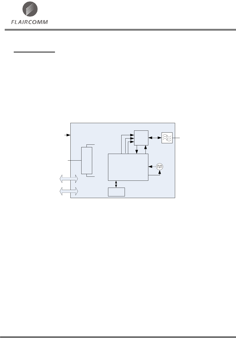
FLC-WFM301 is a tiny, low power and highly economic WiFi radio module that allows OEM to
add wireless capability to their products. The module supports SDIO and CSPI interfaces that make
it simple to design into fully certified embedded WiFi solutions.
The module is an appropriate product for designers who want to add wireless capability to their
products.
1.1 Block Diagram
FEM
CSR6027 / CSR6030
26 MHz
Power Supply
BPF
Antenna
SDIO
or
CSPI
SPI
TX
RX
FEM control
VDD_SDIO
VREG_IN_ANA
VREG_IN_DIG
VDD_RF
Reset
EEPROM
Figure 1: Block Diagram
1.2 Features
Low cost, low power, highly integrated IEEE 802.11b/g/n.
Support Independent Basic Service Set (IBSS), e.g. ad hoc, BSS and Extended Service Set (ESS)
network configurations.
IEEE 802.11n support, including MPDU and MSDU aggregation, immediate block
acknowledgement, PSMP and STBC for improved rate, range and performance.
Intelligent power control, including IEEE802.11 power saving mode.
SDIO (4-bit and 1-bit) and CSPI will be employed to interface with host device (Android, Linux
and WinCE).
Support open system and shared key authentication services.
Internal WEP engine allows 64 or 128 bit Encryption with Temporal Key Integrity Protocol

FLC-WFM301 Datasheet
Flaircomm Microelectronics Confidential
-7-
(TKIP).
Hardware encryption support for WEP40/64, WEP 104/128, TKIP, CCMP (AES), BIP and
CKIP provides functionality for WPA, WPA2, IEEE802.11i, 802.11w and CCX advanced
security mechanisms. Module supports WAPI security in China also.
Support 802.11e Quality of Service (QoS) with WMM Power Save ensures that mobile
solutions can achieve optimal battery life.
Advanced WiFi and BT coexistence schemes provide exceptional performance for WiFi and BT
using a single antenna.
RoHS Compliant.
Support soft AP function and Wi-Fi Direct (FLC-WFM301CL2B only).
1.3 Functions
Transmitter
Receiver
Single antenna BT coexistence
Modulations
IEE802.11b modulations;
1Mbps / 2Mbps / 5.5Mbps / 11Mbps
IEEE802.11g OFDM;
6Mbps / 9Mbps / 12Mbps / 18Mbps / 24Mbps / 36Mbps / 48Mbps / 54Mbps
IEEE802.11n HT modulations MCS0-7, 20MHz, 800 and 400 ns guard interval;
6.5Mbps / 7.2Mbps / 13Mbps / 14.4Mbps / 19.5Mbps / 21.7Mbps / 26.0Mbps /
28.9Mbps / 39.0Mbps / 43.3Mbps / 52.0Mbps / 57.8Mbps / 58.5Mbps / 65.0Mbps /
72.2Mbps
MAC
Comprehensive MAC functionality according to IEEE 802.11-2007, including QoS traffic
scheduling
Support the following optional IEEE802.11n features;
MPDU aggregation
MSDU aggregation
Immediate Block Acknowledgement

FLC-WFM301 Datasheet
Flaircomm Microelectronics Confidential
-8-
PSMP
MTBA
RIFS
L-SIG TXOP protection
Link adaptation using MCS feedback
Encryption
Hardware encryption according to IEEE 802.11-2007 and IEEE802.11w-2009;
WEP40/64
WEP104/128
CCMP(AES)
TKIP
BIP
Hardware encryption support for SMS4 to support WAPI (China)
Hardware encryption support Cisco CKIP
1.4 Applications
Cellular phones
Tablet PCs
Handheld devices
Industrial applications
FLC-WFM301 Datasheet
Flaircomm Microelectronics Confidential
-9-
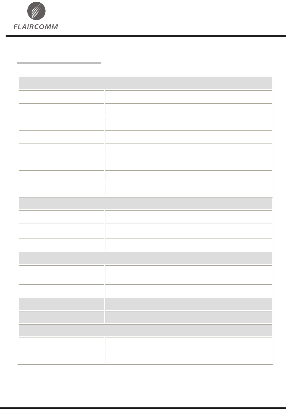
2. General Specification
WiFi Specification
Standard
IEEE 802.11b/g/n
Frequency Band
2.400G~2.4835G
Maximum Data Rate
72.2Mbps
RF Input Impedance
50 ohms
Interface
SDIO(4-bit and 1-bit) and SPI
Sensitivity
-Refer to 5.1
RF TX Power
Refer to 5.1
Encryption
WEP40/64/104/128, CCMP(AES), TKIP, BIP, WAPI
Power
Supply Voltage
1.7 ~ 3.6V DC
Working Current
Refer to Table 12
Standby Current
Refer to Table 12
Operating Environment
Temperature
-40ºC to +85ºC for A and I grade
-20ºC to +70ºC for V and C grade
Humidity
10%~90% Non-Condensing
Certifications
WiFi Alliance/FCC/CE
Environmental
RoHS Compliant
Dimension and Weight
Dimension
8.90mm x 8.90mm x 1.50mm
Weight
<1g
Table 1: General Specification
FLC-WFM301 Datasheet
Flaircomm Microelectronics Confidential
-10-
3. Pin Definition
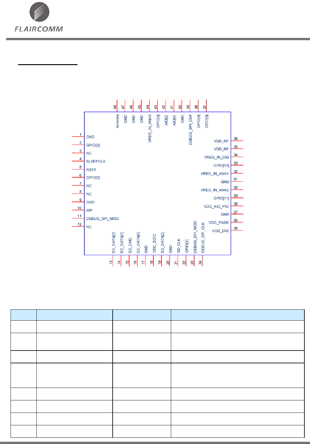
3.1 Pin Configuration
Figure 2: Pin Configuration
3.2 Pin Definition
Pin
Symbol
I/O Type
Description
1
GND
Ground
Ground
2
GPIO[5] (BT_STATE)
I/O
General Purpose Input/Output
(Can be configured for BT coexistence )
3
NC1
I/O
NC
4
SLEEPCLK
I
Sleep Clock Mode: Clock Input for External Sleep
Clock, If only use external 32.768KHz.
Default : using internal clock
5
RST#
I
System reset, active low
6
GPIO[2]
I/O
General Purpose Input/Output
7
NC2
I/O
NC
8
NC
I/O
NC

FLC-WFM301 Datasheet
Flaircomm Microelectronics Confidential
-11-
9
GND
Ground
Ground
10
WP
Reserved for Flaircomm used in production.
Connect to I2C EEPROM WP pin. Internally
pulled high through a 100 k resistor.
11
DEBUG_SPI_MISO
O
DEBUG Data Out
12
NC3
NC
13
SD_DATA[3]
I/O
SDIO 4 bit Mode : Data line bit [3]
SDIO 1 bit Mode : Reserved
SDIO SPI Mode : Card select (Active low)
CSPI Mode: Chip Select
14
SD_DATA[1]
I/O
SDIO 4 bit Mode : Data line bit [1]
SDIO 1 bit Mode : Interrupt
SDIO SPI Mode : Reserved
CSPI Mode: Interrupt
15
SD_CMD
I/O
SDIO 4 bit Mode : Command/Response
SDIO 1 bit Mode : Command Line
SDIO SPI Mode : Data Input
CSPI Mode: MOSI, Data Input
16
SD_DATA[0]
I
SDIO 4 bit Mode : Data Line Bit [0]
SDIO 1 bit Mode : Data Line
SDIO SPI Mode : Data Output
CSPI Mode: MISO, Data output
17
GND
Ground
Ground
18
VDD_SDIO
Power
Voltage Supply for Host Interface (1.7V ~ 3.6V).
19
SD_DATA[2]
I/O
SDIO 4 bit Mode : Data Line Bit [2] or Read Wait
(optional)
SDIO 1 bit Mode : Read Wait (optional)
SDIO SPI Mode : Reserved
CSPI Mode: Not Used
20
GND
Ground
Ground
21
SD_CLK
I
SDIO 4 bit Mode : Clock Input
SDIO 1 bit Mode : Clock Input
SDIO SPI Mode : Clock Input
CSPI Mode: Clock Input
22
GPIO[1]
I/O
General Purpose Input/Output (LED indicator)
23
DEBUG_SPI_MOSI
I
Debug Mode Data In
24
DEBUG_SPI_CLK
I
Debug Mode Clock
25
VDD_DIG
Power
Digital Core Power Supply. This pin is for bypass
cap only. Connect a 2.2uF bypass cap to this pin.
26
VDD_PADS
Power
1.8V power Supply for SPI, RES# and PIO[0] –
PIO[7]
27
GND
Ground
Ground

FLC-WFM301 Datasheet
Flaircomm Microelectronics Confidential
-12-
28
VDD_AIO_PIO
Power
3.3V Power Supply for AIO[0] – AIO[3] and
PIO[8] – PIO[15]
29
GPIO[11]
NC
30
VREG_IN_ANA2
Power
1.45V - 2V Analog Power Supply, for internal
LDO
31
GND
Ground
Ground
32
VREG_IN_ANA1
Power
1.45V - 2V Analog Power Supply, for internal
LDO
33
GPIO[10]
NC
34
VREG_IN_DIG
Power
1.45V - 2V Digital Power Supply, for internal
LDO
35
VDD_RF1
Power
3.3V (2.7 – 4.8V) PA Power Supply (for
FEM_VCC1 / FEM_VCC2)
36
VDD_RF2
Power
3.3V (2.7 – 4.8V) LNA Power Supply (for
FEM_VCC3)
37
GPIO[9]
38
GPIO[4]
(WL_DENY)
O
General Purpose Input/Output
(Can be configured for BT coexistence )
39
DEBUG_SPI_CS#
I/O
DEBUG Mode Select, Active low
Internally Weak Pull-up.
40
GND
Ground
Ground
41
AIO[0]
I/O
Programmable Analogue Input / Output
42
AIO[2]
I/O
Programmable Analogue Input / Output
43
GPIO[3]
(BT_PRIORITY)
I
General Purpose Input / Output
(Can be configured for BT coexistence )
44
VREG_IN_ANA3
Power
1.45V - 2V Analog Power Supply, for internal
LDO
45
GND
Ground
Ground
46
GND
Ground
Ground
47
GND
Ground
Ground
48
Antenna
Analog
RF Input/Output
Table 2: Pin Definition

FLC-WFM301 Datasheet
Flaircomm Microelectronics Confidential
-13-
4. Physical Interfaces
4.1 Power Supply
4.1.1 Linear Regulators
FLC-WFM301 contains four linear regulators:
A low-voltage regulator to supply the 1.2V core digital supply
Three low-voltage regulators for the 1.2V core auxiliary, radio and RF synthesizer analogue supplies
4.1.2 LDO for Digital Supply
VREG_IN_DIG is the input voltage to the internal LDO for digital supply and VDD_DIG is the
output of the LDO. A low ESR 2.2uF capacitor to ground should be connected to this pin.
4.1.3 RF Front End Power Supply
VDD_RF1 and VDD_RF2 are the external 3.3V input to power RF front end. Clean voltage should
be used for these two pins.
4.1.4 I/O Power Supply
VDD_PADS is used to power PIO[0] to PIO[7]. The typical voltage is 1.8V for this rail.
VDD_AIO_PIO is used to power PIO[8] to PIO[15], AIO[0] to AIO[3]
4.2 Reset
WFM301CL can be reset from several sources,
Via the external RST# pin (pin 5)
Via an internal core power supply supervisor
Using software watchdog timers
Via SDIO/CSPI host interface
RST# is an active-low reset input that is internally filtered using the internal low frequency clock
oscillator to avoid spurious resets. A reset occurs after the signal has been asserted for between 250
and 375 s. This pin may be tied to VDD_PADS is unused; otherwise it should be asserted for at
least 1 ms to force a reset.
The power supply monitors VDD_DIG to trigger a power-on-reset. This occurs when the supply
falls below 1.05V (typical) in normal operation or 0.785C (typical) in deep sleep, and ends when the
supply exceeds 1.10V (typical). Glitches of up to 30mV and 2.5s duration, which could be caused
by large load steps, will not trigger a reset.
Each of the internal processors has its own independent watchdog timer to detect and recover from
erroneous software operation. These are typically configured with a timeout of 1.5s, but this may be
increased up to maximum of 64s for reduced power consumption. The watchdogs are enabled at
power-on and continue operating while WFM301CL is in deep sleep.

FLC-WFM301 Datasheet
Flaircomm Microelectronics Confidential
-14-
4.3 RF Interface
The module integrates a band-pass filter to the antenna port which is a 50 port. The user can
connect a 50 antenna directly to the antenna port (pin 48).
4.4 General Purpose Digital IO
There are nine general purpose digital IOs defined in the module. All these GPIOs can be configured
by software to realize various functions, such as button controls, LED displays or interrupt signals to
host controller, etc. Do not connect them if not use.
GPIO pin
Function Assignment
GPIO[1]
BT-Coexistence or other (1.8V)
GPIO[2]
BT-Coexistence or other (1.8V)
GPIO[3]
BT-Coexistence or other (1.8V)
GPIO[4]
BT-Coexistence or other (1.8V)
GPIO[5]
BT-Coexistence or other (1.8V)
GPIO[9]
GPIO (3.3V)
GPIO[10]
GPIO (3.3V)
GPIO[11]
GPIO (3.3V)
Table 3: GPIO Usage
4.5 Analog IO
AIO Pin
Assignment
AIO[0]
Analog IO (3.3V)
AIO[2]
Analog IO (3.3V)
Table 4: Analog IO Usage
4.6 Host Interfaces
WFM301CL has a single host interface port that can be configured into one of four modes:
SD 1-bit
SD 4-bit
SDIO SPI
CSPI
The first three modes operate according to the SD Card specifications. The fourth mode is a CSR
proprietary variant designed to allow more efficient implementation on hosts without dedicated
SDIO host controller. Table 5 shows the usage of the host interfaces pins in each mode.
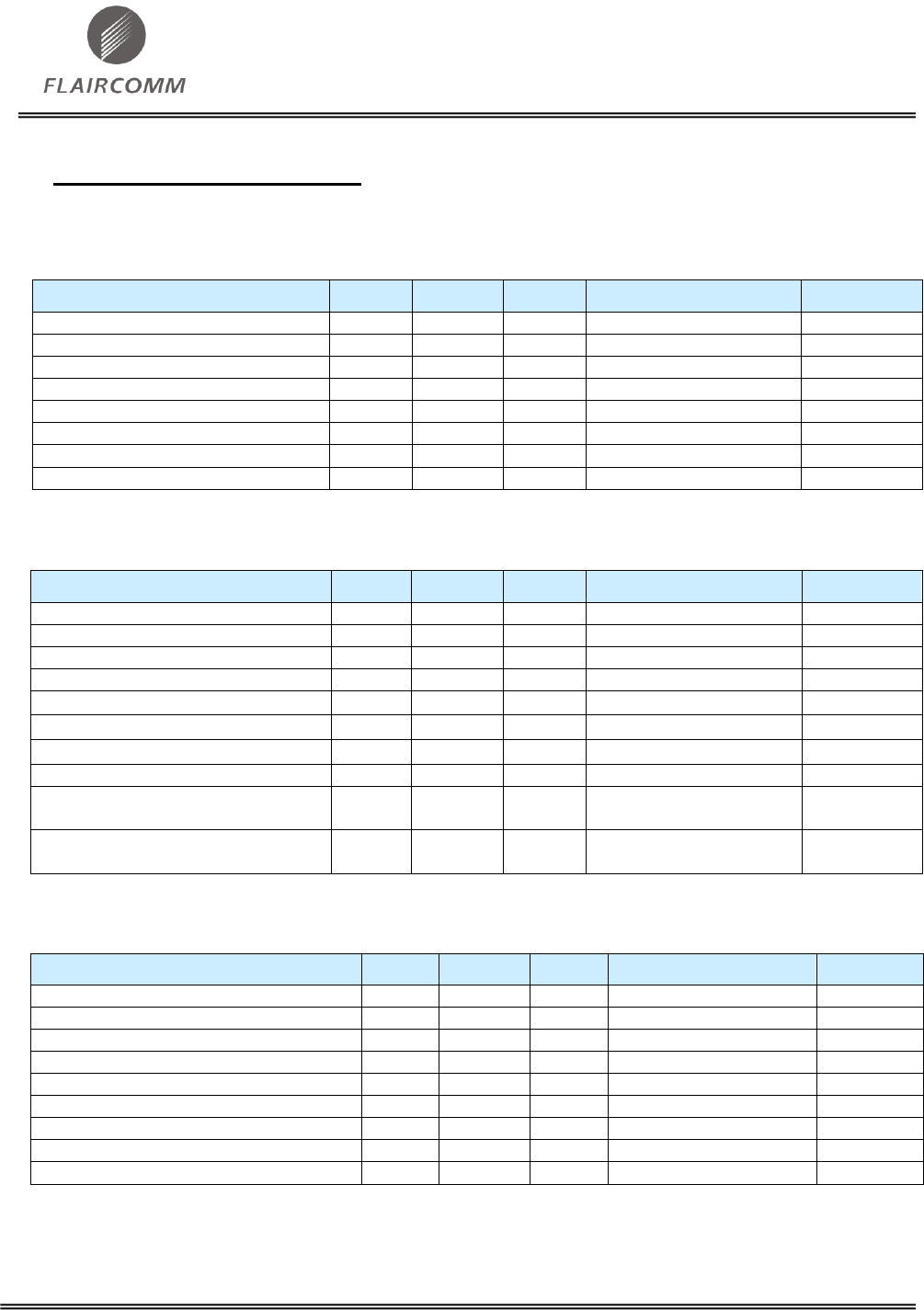
Pin Name
SD 1-bit
SD 4-bit
SD SPI
CSPI
SD_CLK
CLK: Clock
CLK: Clock
SCLK: Clock
CLK: Clock
SD_CMD
CMD: Commend line
CMD: Command line
DI: Data input
MOSI: Data input

FLC-WFM301 Datasheet
Flaircomm Microelectronics Confidential
-15-
SD_DATA[0]
DATA: Data line
DAT[0]: Data line 0
DO: Data output
MISO: Data output
SD_DATA[1]
IPQ#: Interrupt
DAT[1]: Data line 1
IRQ#: Interrupt
IRQ#: Interrupt
SD_DATA[2]
RW: Read wait
DAT[2]: Date line 2
Not used
Not used
SD_DATA[3]
CD: Card detect
DAT[3]: Date line 3
CS#: Card select
CS#: Card select
Table 5: Analog IO Usage
All four modes provide identical access to on-chip registers and support clock speeds of up to
50MHz for a maximum burst rate of 200Mbits/s (in SD 4-bit mode). At power-on the host interface
starts in SD 1-bit mode and may be switched into any of the alternative modes via SDIO commands.
4.6.1 SDIO
SDIO mode fully support SDIO specification version 2.00. It supports all defined slave modes (SD 1
bit, SD 4-bit and SDIO SPI), but not SD host functionality.
Two functions are supported:
Function 0 is the mandatory function used for card configuration. This includes the CCCR, FBR and CIS. Vender-
defined registers within the CCCR support sleep and wake-up signaling.
Function 1 provides access to the IEEE 802.11 functionality. IO_RW_DIRECT (CMD52) reads and writes on-chip
registers and memory locations directly. IO_RW_EXTENDED (CMD53) transfers blocks of data to or from the
on-chip MMU buffers.
The SDIO interface implements a subset of optional features. Specifically it supports:
Continuous SPI interrupt (SCSI)
Direct Commands during data transfer (SDC)
Multi-block (SMB)
Read wait (SRW)
4.6.1.1 SDIO Sleep Signaling
WFM301CL supports a variety of mechanisms to enable both itself and the host to efficiently enter
and leave low-power modes.
4.6.1.1.1 Card Sleep and Wake-up
WFM301CL automatically uses its sleep modes to minimize power consumption. Registers in
function 0 are always directly accessible by the host, irrespective of the device’s sleep modes.
Attempts to access function 1 while the device is in deep sleep are likely to results in SDIO timeouts.
To avoid the need for the host to implement complicated retry mechanisms, a simple deep sleep
control scheme is supported via a Vender Unique Register within the CCCR in function 0. The host
uses this register to tell WFM301CL when it is allowed to use deep sleep. When the host
subsequently needs to access function 1 it uses the same register to initiated a wake-up and them
waits for an SDIO interrupt to indicate that the wake-up is compete.

FLC-WFM301 Datasheet
Flaircomm Microelectronics Confidential
-16-
4.6.1.2 Host Sleep and Wake-up
The normal method for WFM301CL to wake the host up is via the in-band interrupt on
SDIO_DATA[1]. This is the dame mechanism that is used to notify the host of received data or
interesting events; no explicit sleep signaling is required.
An alternative out-of-band mechanism is provided for hosts that cannot utilize the SDIO interrupt as
a wake-up signal, e.g. where a separate power-management IC needs to restore power to the host
processor. This feature is enabled by masking out SDIO interrupts via the Int Enable register within
the CCCR in function 0. When an SDIO interrupt would have been signaled otherwise, a pulse is
instead generated on a configured PIO line.
Note: The out-of-band wake-up signal is not a replacement for the in-band SDIO interrupt. The standard interrupt signal
should be used for data transfer during normal operation.
FLC-WFM301 Datasheet
Flaircomm Microelectronics Confidential
-17-
5. Electrical Characteristic
5.1 WiFi Performance Specifications
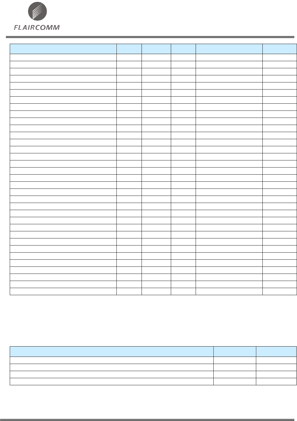
5.1.1 DSSS and CCK modulations (802.11b) TX Performance Specifications
Min
Typical
Max
IEEE Specification
Unit
Frequency range
2400
-
2500
-
MHz
RMS transmit power(a)
16
18
20
-
dBm
RMS EVM
0
3.5
20
35
%
Spectral mask 1st Sidelobe
-
-39
-33
-30
dBr
Spectral mask 2nd Sidelobe
-
-54
-50
-50
dBr
RF carrier suppression
-
-30
-25
-15
dB
Center Frequency Tolerance
-20
2
+20
25
ppm
Occupied Bandwidth
22
MHz
Table 6: DSSS and CCK modulations (802.11b) TX Performance Specifications
5.1.2 OFDM TX Performance Specifications
Min
Typical
Max
IEEE Specification
Unit
Frequency range
2400
-
2500
-
MHz
RMS transmit power(a)
12
14
18
-
dBm
RMS EVM,54Mbps
-
-29
-25
-25
dB
RMS EVM,mcs7
-
-29
-28
-28
dB
Spectral mask,±11MHz
-
-35
-30
-20
dBr
Spectral mask,±20MHz
-
-40
-30
-28
dBr
Spectral mask±30MHz
-
-50
-42
-40
dBr
Centre frequency leakage
-
-35
-25
-15
dB
Spectral flatness for spectral lines -16
to -1,1 to 16
-
-
±2
±2
dB
Spectral flatness for spectral lines -26
to -17,17 to 26
-
-
-4 to 2
-4 to 2
dB
Table 7: OFDM TX Performance Specifications
5.1.3 DSSS and CCK modulations (802.11b) RX Performance Specifications
Min
Typical
Max
IEEE Specification
Unit
Frequency range
2400
-
2500
-
MHz
Rx sensitivity,1Mbps DSSS(a)
-
-92
-90
-
dBm
Rx sensitivity,2Mbps DSSS(a)
-
-90
-88
-80
dBm
Rx sensitivity,5.5Mbps DSSS(a)
-
-88
-87
-
dBm
Rx sensitivity,11Mbps DSSS(a)
-
-87
-83
-76
dBm
Maximum input level, DSSS(a)
-4
0
-
-4
dBm
Maximum input level, CCK(a)
-5
-1
-
-10
dBm
Adjacent channel rejection, DSSS(b)
35
51
-
35
dB
Adjacent channel rejection, CCK(b)
35
48
-
35
dB
Table 8: OFDM TX Performance Specifications
5.1.4 OFDM RX Performance Specifications
FLC-WFM301 Datasheet
Flaircomm Microelectronics Confidential
-18-
Min
Typical
Max
IEEE Specification
Unit
Frequency range
2400
-
2500
-
MHz
Rx sensitivity,6Mbps(a)(b)
-
-89
-84
-82
dBm
Rx sensitivity,9Mbps(a)(b)
-
-88
-82
-81
dBm
Rx sensitivity,12Mbps(a)(b)
-
-87
-82
-79
dBm
Rx sensitivity,18Mbps(a)(b)
-
-85
-78
-77
dBm
Rx sensitivity,24Mbps(a)(b)
-
-82
-76
-74
dBm
Rx sensitivity,36Mbps(a)(b)
-
-79
-73
-70
dBm
Rx sensitivity,48Mbps(a)(b)
-
-74
-69
-66
dBm
Rx sensitivity,54Mbps(a)(b)
-
-72
-68
-65
dBm
Rx sensitivity,MCS0(a)(c)
-
-90
-84
-82
dBm
Rx sensitivity, MCS1(a)(c)
-
-87
-81
-79
dBm
Rx sensitivity, MCS2(a)(c)
-
-84
-78
-77
dBm
Rx sensitivity, MCS3(a)(c)
-
-81
-76
-74
dBm
Rx sensitivity, MCS4(a)(c)
-
-78
-70
-70
dBm
Rx sensitivity, MCS5(a)(c)
-
-73
-66
-66
dBm
Rx sensitivity, MCS6(a)(c)
-
-71
-65
-65
dBm
Rx sensitivity, MCS7(a)(c)
-
-69
-
-64
dBm
Maximum input level(d)
-5
-1
-
-20
dBm
Adjacent channelrejection,6Mbps(e)
16
27
-
16
dB
Adjacent channel rejection,9Mbps(e)
15
26
-
15
dB
Adjacent channel rejection,12Mbps(e)
13
25
-
13
dB
Adjacent channel rejection,18Mbps(e)
11
25
-
11
dB
Adjacent channel rejection,24Mbps(e)
8
23
-
8
dB
Adjacent channel rejection,36Mbps(e)
4
20
-
4
dB
Adjacent channel rejection,48Mbps(e)
0
16
-
0
dB
Adjacent channel rejection,54Mbps(e)
-1
14
-
-1
dB
Adjacent channel rejection,MCS0(e)
16
27
-
16
dB
Adjacent channel rejection,MCS1(e)
13
25
-
13
dB
Adjacent channel rejection,MCS2(e)
11
21
-
11
dB
Adjacent channel rejection,MCS3(e)
8
22
-
8
dB
Adjacent channel rejection,MCS4(e)
4
16
-
4
dB
Adjacent channel rejection,MCS5(e)
0
13
-
0
dB
Adjacent channel rejection,MCS6(e)
-1
10
-
-1
dB
Adjacent channel rejection,MCS7(e)
-2
6
-
-2
dB
Table 9: OFDM RX Performance Specifications
5.2 DC Electrical Specifications
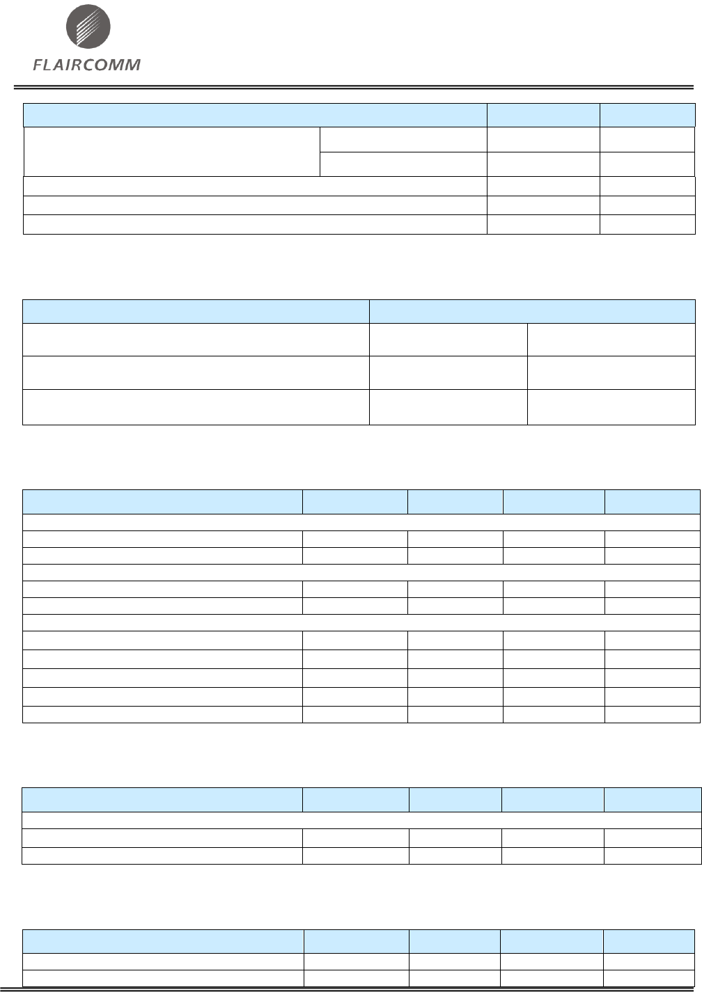
5.2.1 Absolute Maximum Ratings
Rating
Min
Max
Storage temperature
-40°C
85°C
Linear regulator voltage (VREG_EN)
-0.4V
2.5V
I/O supply voltage (VDD_SDIO,VDD_PADS_PIO_0_7,VDD_AIO_PIO_8_15)
1.7V
3.6V
Other terminal voltages
VSS-0.3V
VDD+0.3V
Table 10: Absolute Maximum Ratings
5.2.2 Recommended Operating Conditions
FLC-WFM301 Datasheet
Flaircomm Microelectronics Confidential
-19-
Operating Condition
Min
Max
Operating Temperature Range
for A and I grade
-40 ºC
+85 ºC
for V and C grade
-20 ºC
+70 ºC
Host interface I/O supply voltage (VDD_SDIO)
1.7V
3.6V
Other I/O supply voltage (VDD_PADS_PIO_0_7, VDD_AIO_PIO_8_15)
1.7V
3.3V
Linear regulator supply voltage (VREG_IN_DIG, VREG_IN_ANA)
1.45V
2.0V
Table 11: Recommended Operating Conditions
5.2.3 Current Consumption
State
Power Consumption
Continuous receive (2.4GHz OFDM)
135mA @1.8V
10mA @3.3V
276mW
Continuous transmit (2.4GHz OFDM)
160mA @1.8V
155mA @3.3V
800mW
Leakage (deep sleep, including internal sleep clock )
66μA @1.8V
5A @3.3V
135W
Table 12: Current Consumption
5.2.4 Digital Characteristics
Digital Terminals
Min
Typical
Max
Unit
Input Voltage Levels
VIL input logic level low
-0.3
-
0.25VDD
V
VIH input logic level high
0.625VDD
-
VDD+0.3
V
Output Voltage Levels
VOL output logic Level low, IOL=8.0mA
-
-
0.4
V
VOH output logic Level high, IOH=-8.0mA
0.75VDD
-
VDD
V
Input and Tri-state Currents
Strong pull-up
-150
-40
-10
μA
Strong pull-down
10
40
150
μA
Weak pull-up
-5
-1.0
-0.33
μA
Weak pull-down
0.33
1.0
5.0
μA
CI Input Capacitance
1.0
-
5.0
pF
Table 13: Digital Characteristics
5.2.5 Clock Characteristics
Clock Source
Min
Typical
Max
Unit
External Clock
XTAL_IN input resistance
30
-
-
kΩ
XTAL_IN input capacitance
-
-
4
pF
Table 14: Clock Characteristics
5.2.6 Power-on Reset Characteristics
Power-on Reset
Min
Typical
Max
Unit
Reset release on VDD_DIG rising(HL)
1.030
-
1.150
V
Reset assert on VDD_DIG falling(LO)
HL-0.060
-
HL-0.045
V

FLC-WFM301 Datasheet
Flaircomm Microelectronics Confidential
-20-
Reset assert on VDD_DIG falling(Sleep mode)
0.770
0.785
0.800
V
Table 15: Power-on Reset Characteristics
FLC-WFM301 Datasheet
Flaircomm Microelectronics Confidential
-21-
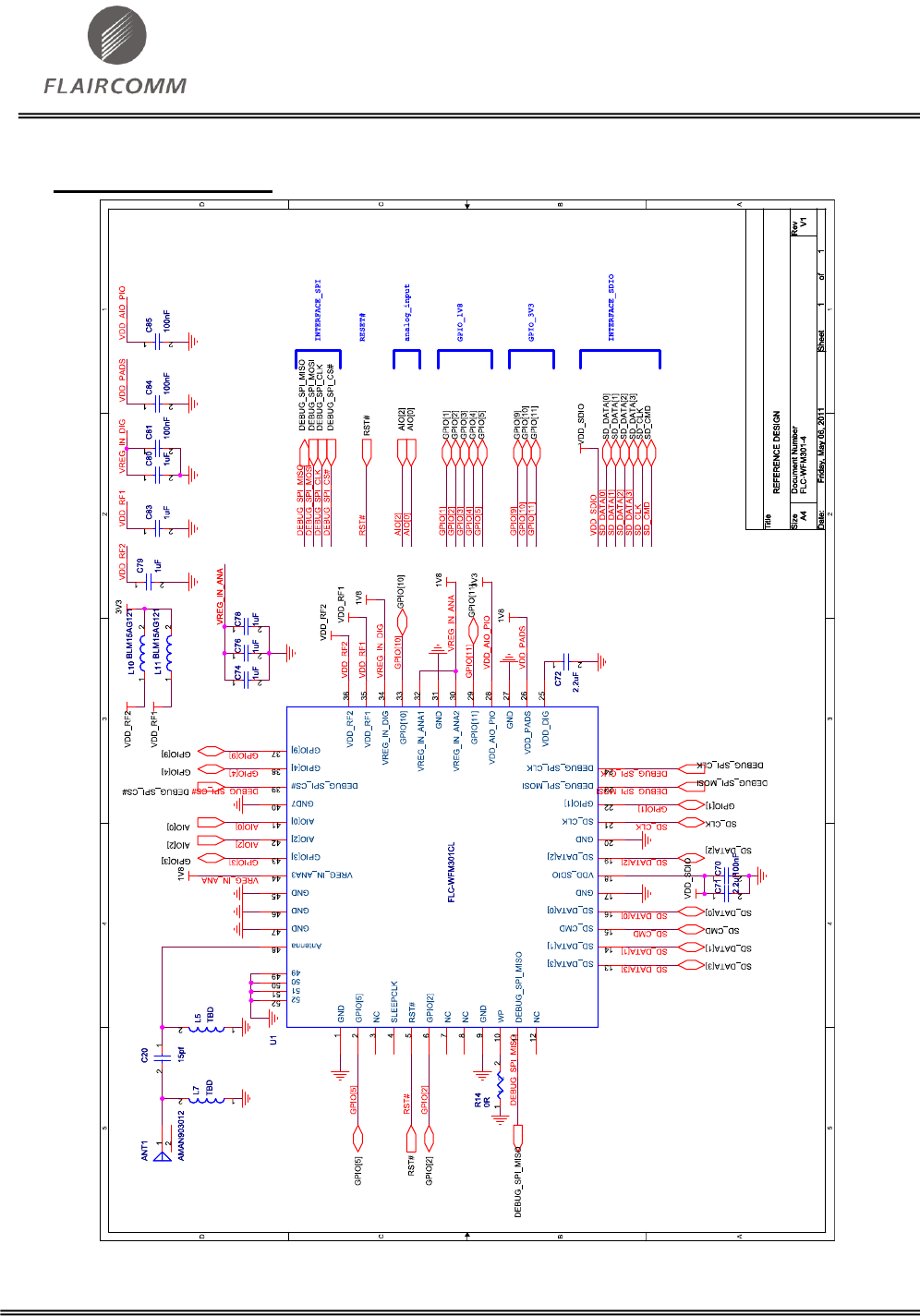
6. Reference Design
Figure 3: Reference Design
FLC-WFM301 Datasheet
Flaircomm Microelectronics Confidential
-22-
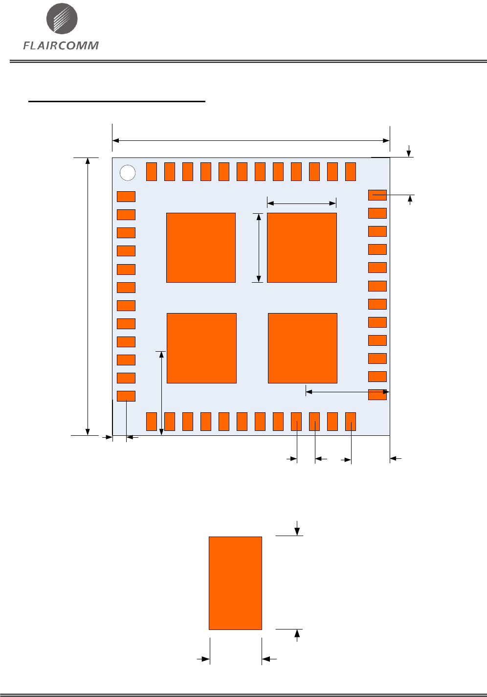
7. Mechanical Characteristic
8.90±0.1
8.90±0.1
2.30±0.1
2.30±0.1
3.05±0.1
3.05±0.1
0.6±0.1 1.15±0.05
1.15±0.05
0.5±0.05
Figure 4: Mechanical Characteristic
0.35±0.05
0.60±0.05
Figure 5: Pad Size
FLC-WFM301 Datasheet
Flaircomm Microelectronics Confidential
-23-
8. Recommended PCB Layout and Mounting Pattern
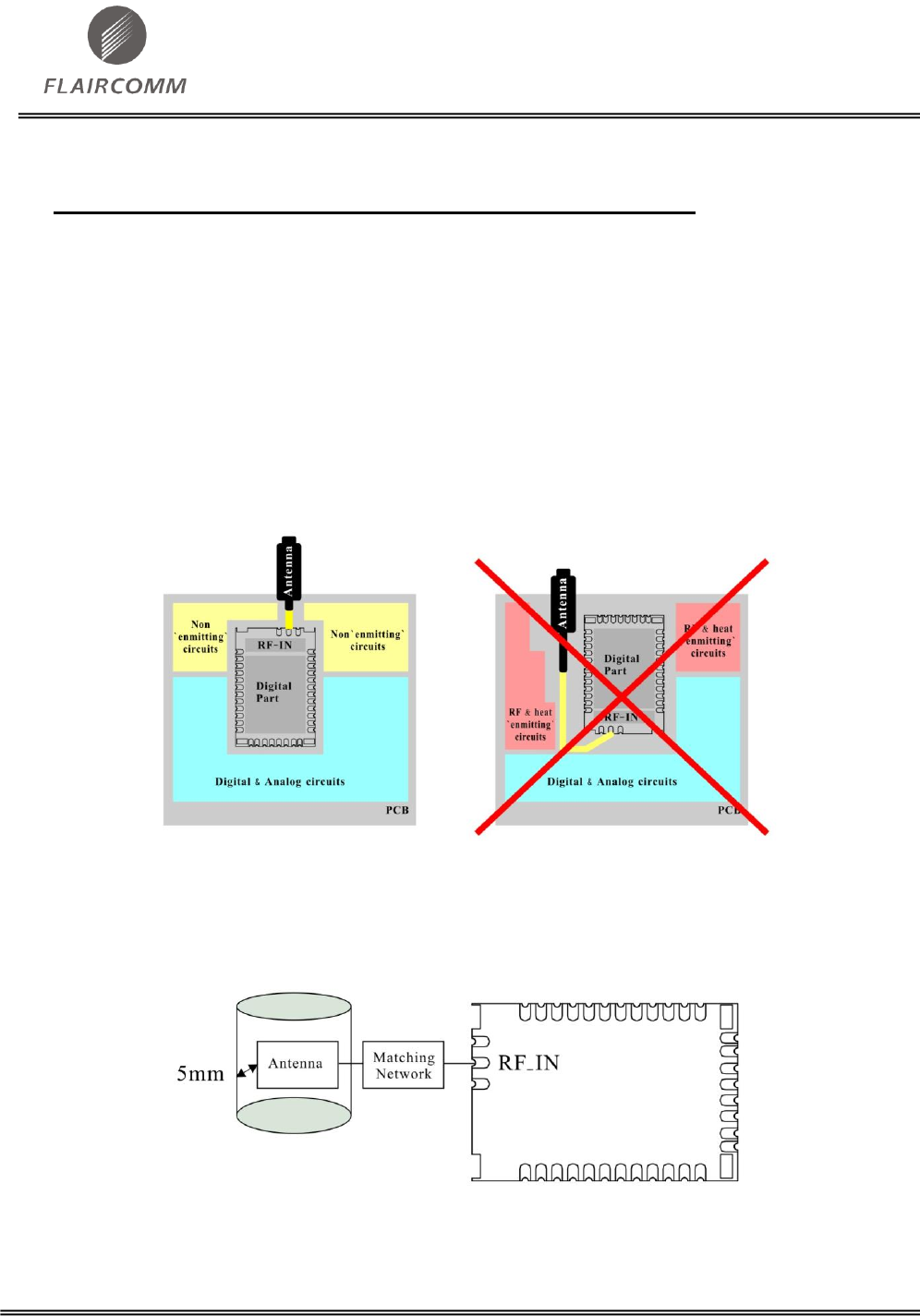
Placement and PCB layout are critical to optimize the performances of a module without on-board
antenna designs. The trace from the antenna port of the module to an external antenna should be 50
and must be as short as possible to avoid any interference into the transceiver of the module. The
location of the external antenna and RF-IN port of the module should be kept away from any noise
sources and digital traces. A matching network might be needed in between the external antenna and
Antenna port to better match the impedance to minimize the return loss.
As indicated in Figure 6 below, RF critical circuits of the module should be clearly separated from
any digital circuits on the system board. All RF circuits in the module are close to the antenna port.
The module, then, should be placed in this way that module digital part towards your digital section
of the system PCB.
Figure 6: Placement the Module on a System Board
8.1 Antenna Connection and Grounding Plane Design
Figure 7: Leave 5mm Clearance Space from the Antenna
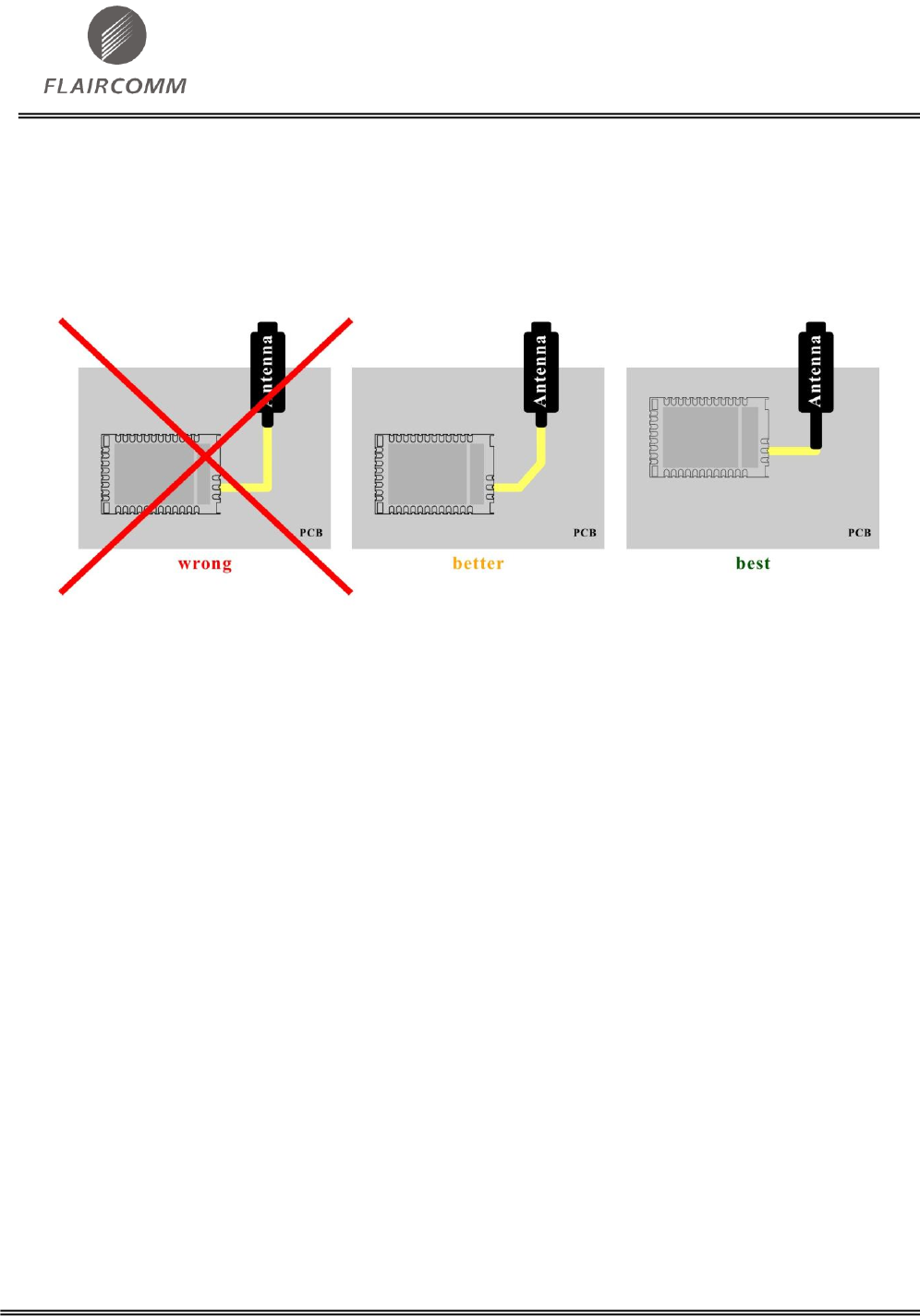
General design recommendations are:
The length of the trace or connection line should be kept as short as possible.
FLC-WFM301 Datasheet
Flaircomm Microelectronics Confidential
-24-
Distance between connection and ground area on the top layer should at least be as large as the
dielectric thickness.
Routing the RF close to digital sections of the system board should be avoided.
To reduce signal reflections, sharp angles in the routing of the micro strip line should be avoided.
Chamfers or fillets are preferred for rectangular routing; 45-degree routing is preferred over
Manhattan style 90-degree routing.
Figure 8: Recommended Trace Connects Antenna and the Module
Routing of the RF-connection underneath the module should be avoided.
Use as many vias as possible to connect the ground planes.
FLC-WFM301 Datasheet
Flaircomm Microelectronics Confidential
-25-
9. Recommended Reflow Profile
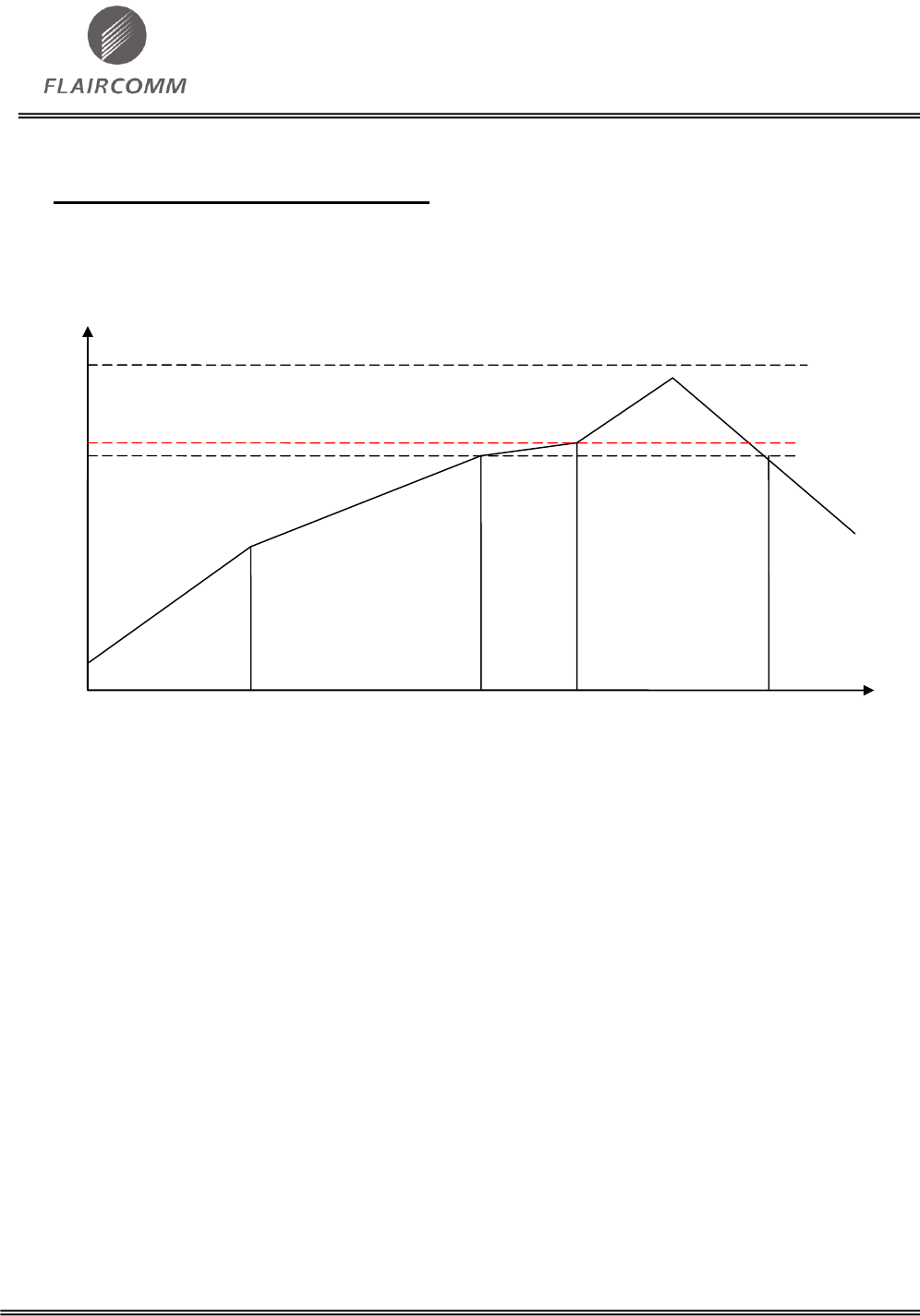
The soldering profile depends on various parameters necessitating a set up for each application. The
data here is given only for guidance on solder reflow.
210
217
℃
250
A
B
C
D
1
2
0
25
3
4
5
6
min
E
Figure 9: Recommended Reflow Profile
Pre-heat zone (A) — This zone raises the temperature at a controlled rate, typically 0.5 – 2 C/s.
The purpose of this zone is to preheat the PCB board and components to 120 ~ 150 C. This stage is
required to distribute the heat uniformly to the PCB board and completely remove solvent to reduce
the heat shock to components.
Equilibrium Zone 1 (B) — In this stage the flux becomes soft and uniformly encapsulates solder
particles and spread over PCB board, preventing them from being re-oxidized. Also with elevation
of temperature and liquefaction of flux, each activator and rosin get activated and start eliminating
oxide film formed on the surface of each solder particle and PCB board. The temperature is
recommended to be 150 to 210 for 60 to 120 second for this zone.
Equilibrium Zone 2 (c) (optional) — In order to resolve the upright component issue, it is
recommended to keep the temperature in 210 – 217 for about 20 to 30 second.
Reflow Zone (D) — The profile in the figure is designed for Sn/Ag3.0/Cu0.5. It can be a reference
for other lead-free solder. The peak temperature should be high enough to achieve good wetting but
not so high as to cause component discoloration or damage. Excessive soldering time can lead to
intermetallic growth which can result in a brittle joint. The recommended peak temperature (Tp) is
230 ~ 250 C. The soldering time should be 30 to 90 second when the temperature is above 217 C.
Cooling Zone (E) — The cooling ate should be fast, to keep the solder grains small which will give
a longer-lasting joint. Typical cooling rate should be 4 C.
FLC-WFM301 Datasheet
Flaircomm Microelectronics Confidential
-26-
10. Ordering Information
10.1 Product Packaging Information
Figure 10: Product Packaging Information
10.2 Ordering information
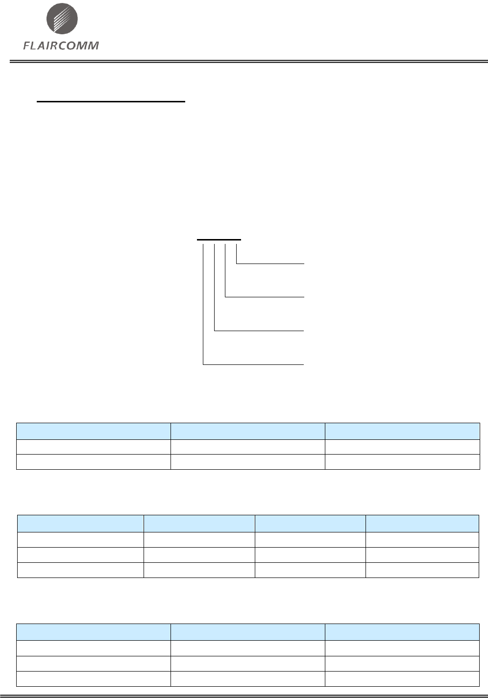
FLC-WFM301XYZA
Product Revision
Shipping Package
Product Package
Product Grade
Figure 11: Ordering Information
10.2.1 Product Revision
Product Revision
Description
Availability
A
With CSR6027
Yes
B
With CSR6030
Yes
Table 16: Product Revision
10.2.2 Shipping Package
Shipping Package
Description
Quantity
Availability
0
Foam Tray
—
No
1
Plastic Tray
—
No
2
Tape
1500
Yes
Table 17: Shipping Package
10.2.3 Product Package
Product Package
Description
Availability
Q
QFN
No
L
LGA
Yes
B
BGA
No

FLC-WFM301 Datasheet
Flaircomm Microelectronics Confidential
-27-
C
Connector
No
Table 18: Product Package
10.2.4 Product Grade
Product Grade
Description
Availability
C
Consumer
Yes
I
Industrial
Yes
V
Automobile After-Market
Yes
A
Automobile Before-Market
No
Table 19: Product Grade

FLC-WFM301 Datasheet
Flaircomm Microelectronics Confidential
-28-
11. Cautions &Warnings
11.1 FCC Statement
1. This device complies with Part 15 of the FCC Rules. Operation is subject to the following two
conditions:
(1) This device may not cause harmful interference.
(2) This device must accept any interference received, including interference that may cause
undesired operation.
2. Changes or modifications not expressly approved by the party responsible for compliance could
void the user's authority to operate the equipment.
NOTE: This equipment has been tested and found to comply with the limits for a Class B digital
device, pursuant to Part 15 of the FCC Rules. These limits are designed to provide reasonable
protection against harmful interference in a residential installation.
This equipment generates uses and can radiate radio frequency energy and, if not installed and used
in accordance with the instructions, may cause harmful interference to radio communications.
However, there is no guarantee that interference will not occur in a particular installation. If this
equipment does cause harmful interference to radio or television reception, which can be determined
by turning the equipment off and on, the user is encouraged to try to correct the interference by one
or more of the following measures:
Reorient or relocate the receiving antenna.
Increase the separation between the equipment and receiver.
Connect the equipment into an outlet on a circuit different from that to which the receiver is
connected.
Consult the dealer or an experienced radio/TV technician for help.
This radio module must not be installed to co-locate and operate simultaneously with other radios in
host system; additional testing and equipment authorization may be required to operating
simultaneously with other radios.
11.2 FCC Radiation Exposure Statement
This equipment complies with FCC radiation exposure limits set forth for an uncontrolled
environment. This equipment should be installed and operated with minimum distance 20cm
between the radiator & your body.
11.3 FLC-WFM301 Label Instructions
The FLC-WFM301 module is designed to comply with the FCC statements.
FLC-WFM301 Datasheet
Flaircomm Microelectronics Confidential
-29-
The packaging of host system that uses WFM301 should display a label indicating the information
as follows:
Contains FCC ID: P4IWFM301
Model: FLC-WFM301 (with CSR6030)
(Series models: FLC-WFM301IL2B/FLC-WFM301VL2B/FLC-WFM301CL2B)
Any similar wording that expresses the same meaning may also be used.
11.4 FLC-BTM301 Antenna Statement
11.4.1 Antenna Electrical Specifications
Part
Number
Frequency Range
(GHz)
Temperature
Average
Gain
VSWR
Impedance
ALA931C5
2.4~ 2.485
21.5°C typ.
-3 dBi min.
2.5:1 max.
50 Ω
Table 20: Antenna Electrical Specifications
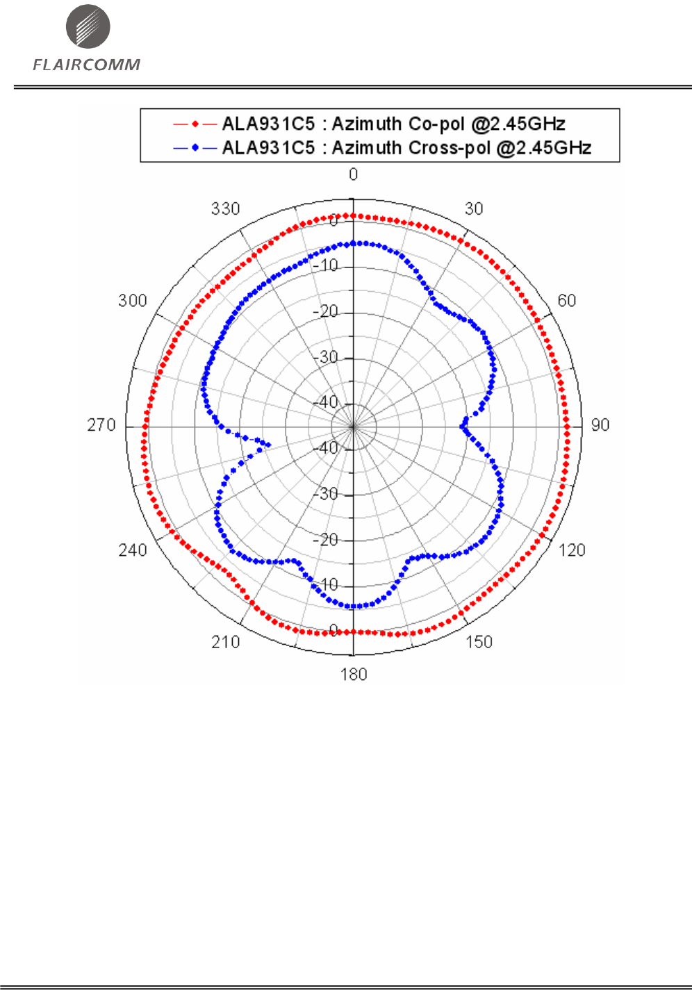
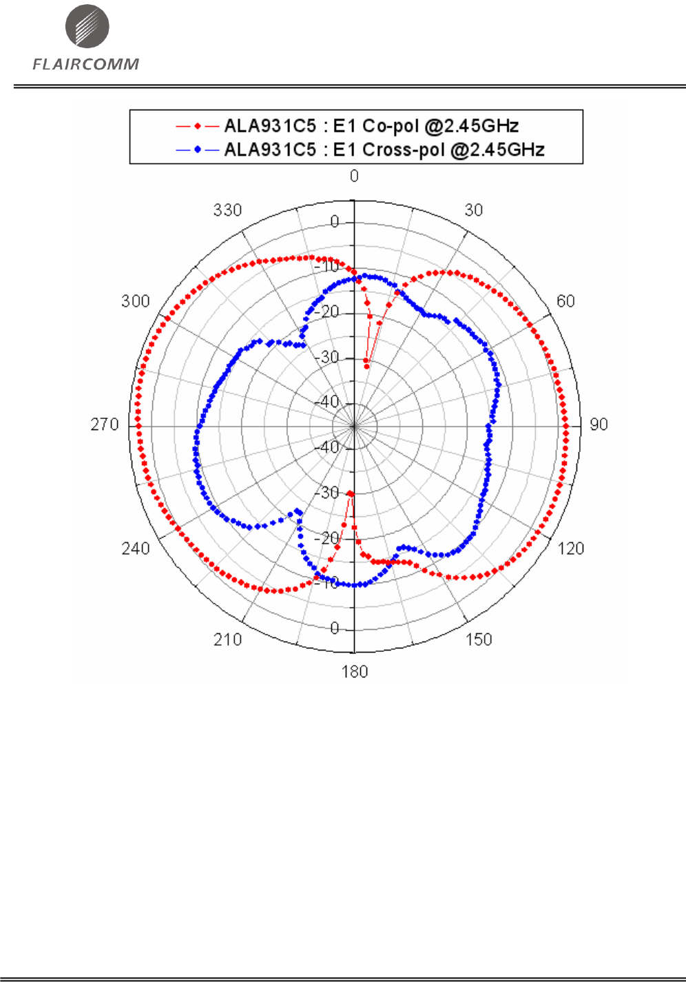
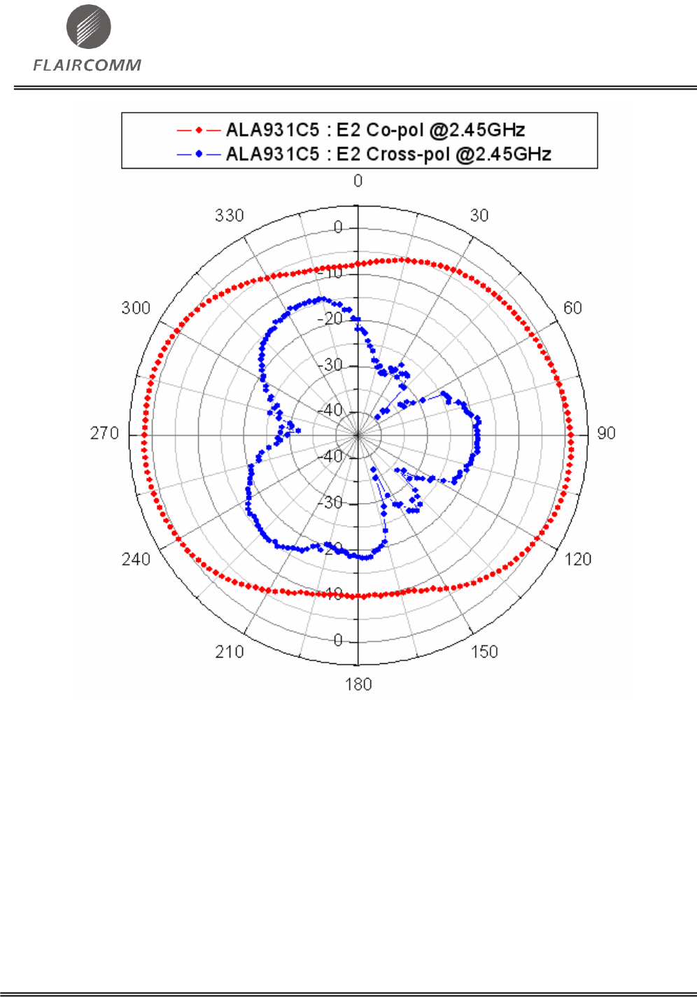
11.4.2 Radiation Gain and Pattern
Peak Gain(dBi)
Average Gain(dBi)
Remark
Azimuth
2.8
1.0
@2.45 GHz
Elevation 1
3.5
-0.7
@2.45 GHz
Elevation 2
1.7
-1.6
@2.45 GHz
Table 21: Radiation Gain and Pattern
FLC-WFM301 Datasheet
Flaircomm Microelectronics Confidential
-30-
Figure 12: ALA931C5 Radiation Pattern : Azimuth@2.45GHz
FLC-WFM301 Datasheet
Flaircomm Microelectronics Confidential
-31-
Figure 13: ALA931C5 Radiation Pattern : Elevation1@2.45GHz
FLC-WFM301 Datasheet
Flaircomm Microelectronics Confidential
-32-
Figure 14: ALA931C5 Radiation Pattern : Elevation2@2.45GHz