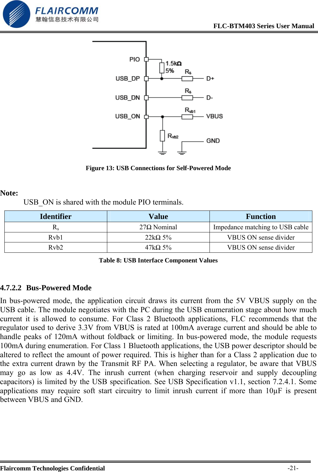
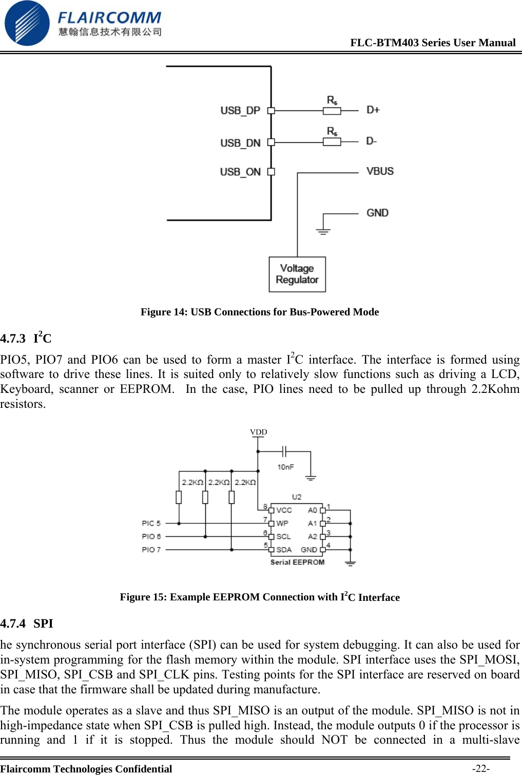
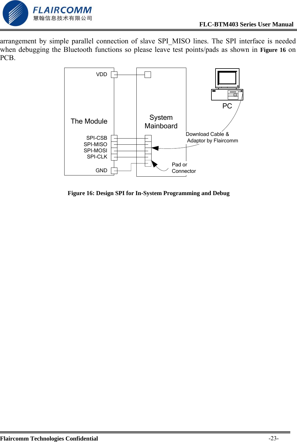
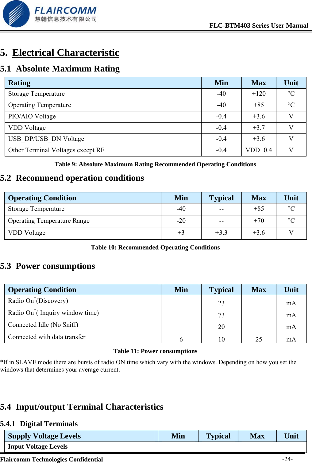
Flaircomm Technologies BTM403 Bluetooth Module User Manual FLC BTM401 DS
Flaircomm Technologies Inc. Bluetooth Module FLC BTM401 DS
UserManual.wiki
>
Flaircomm Technologies
>
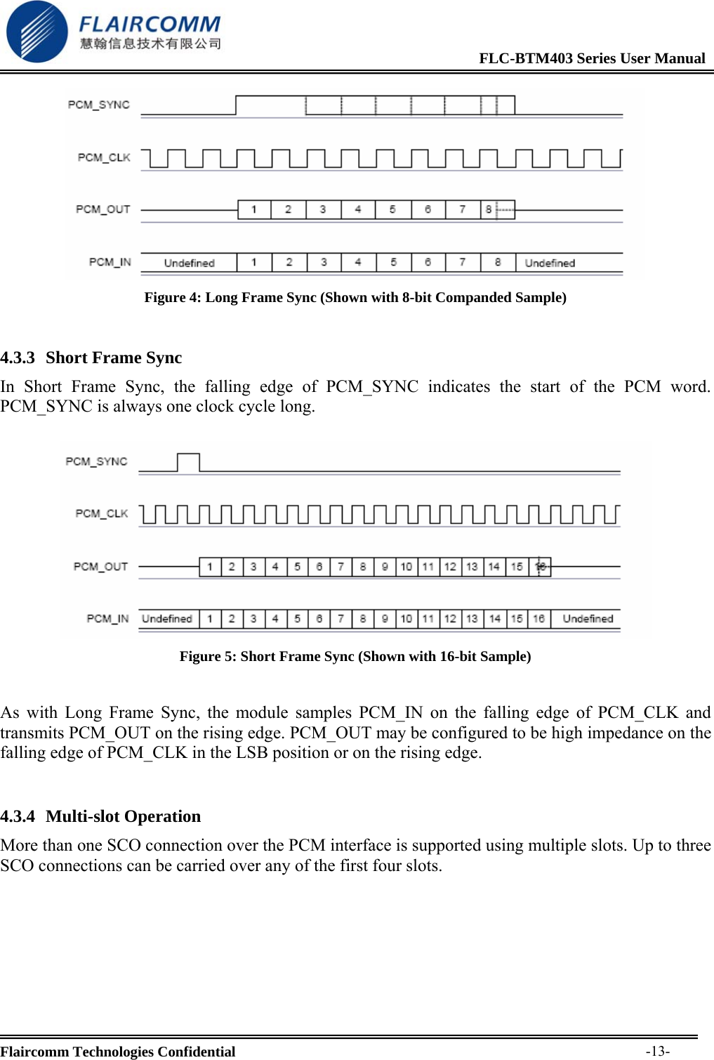
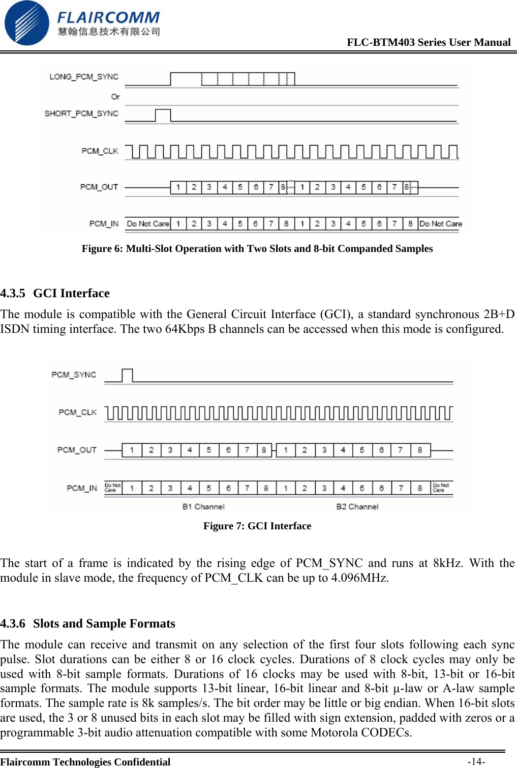
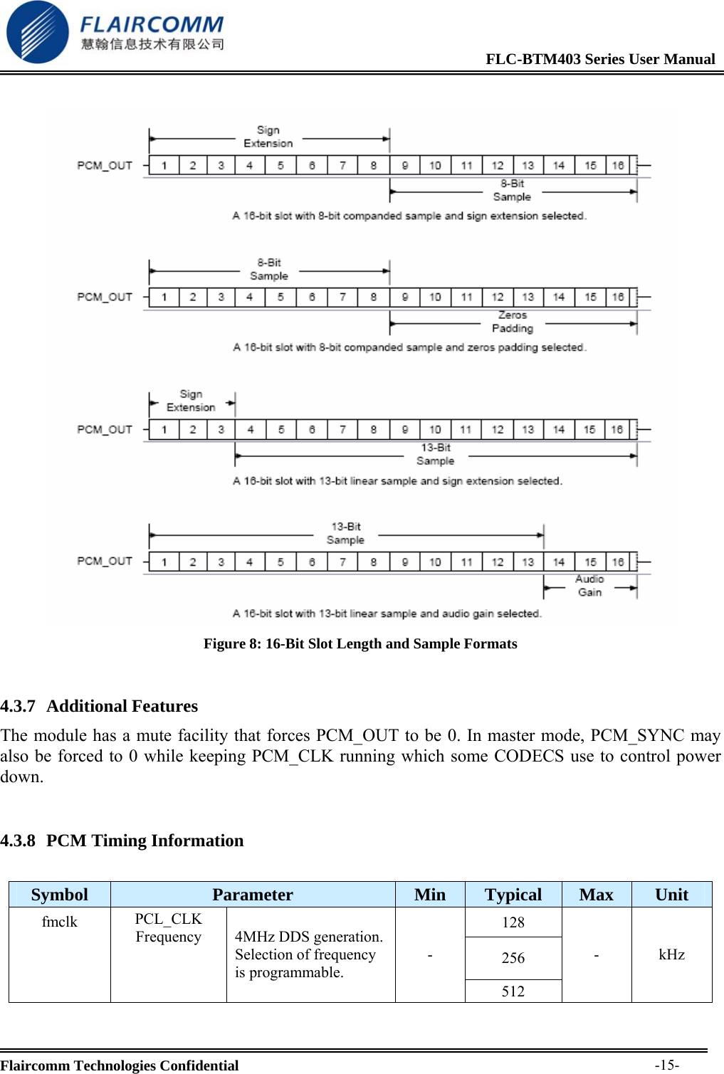
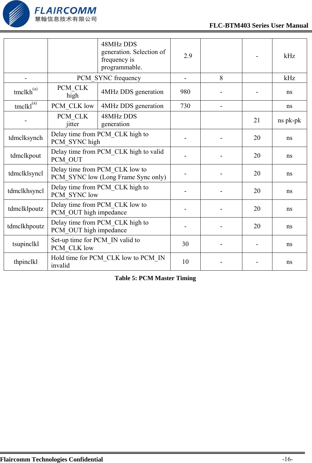
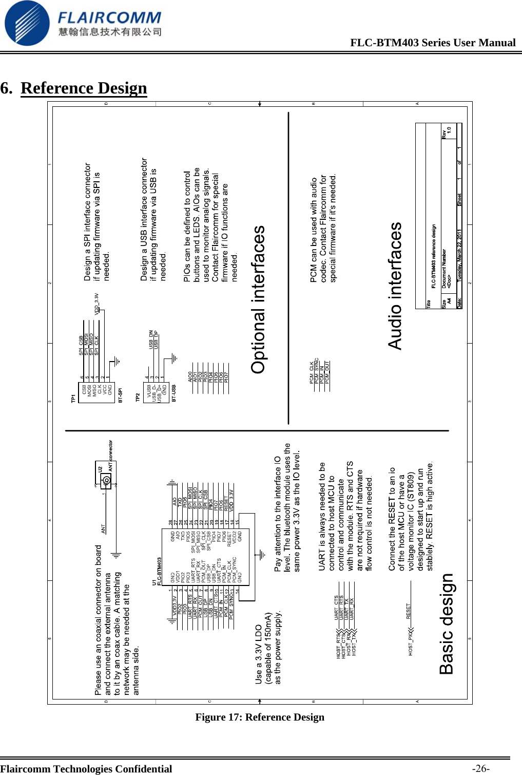
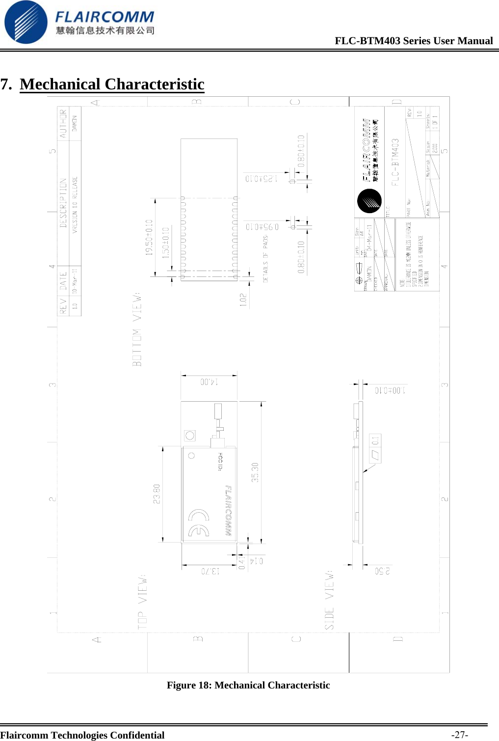
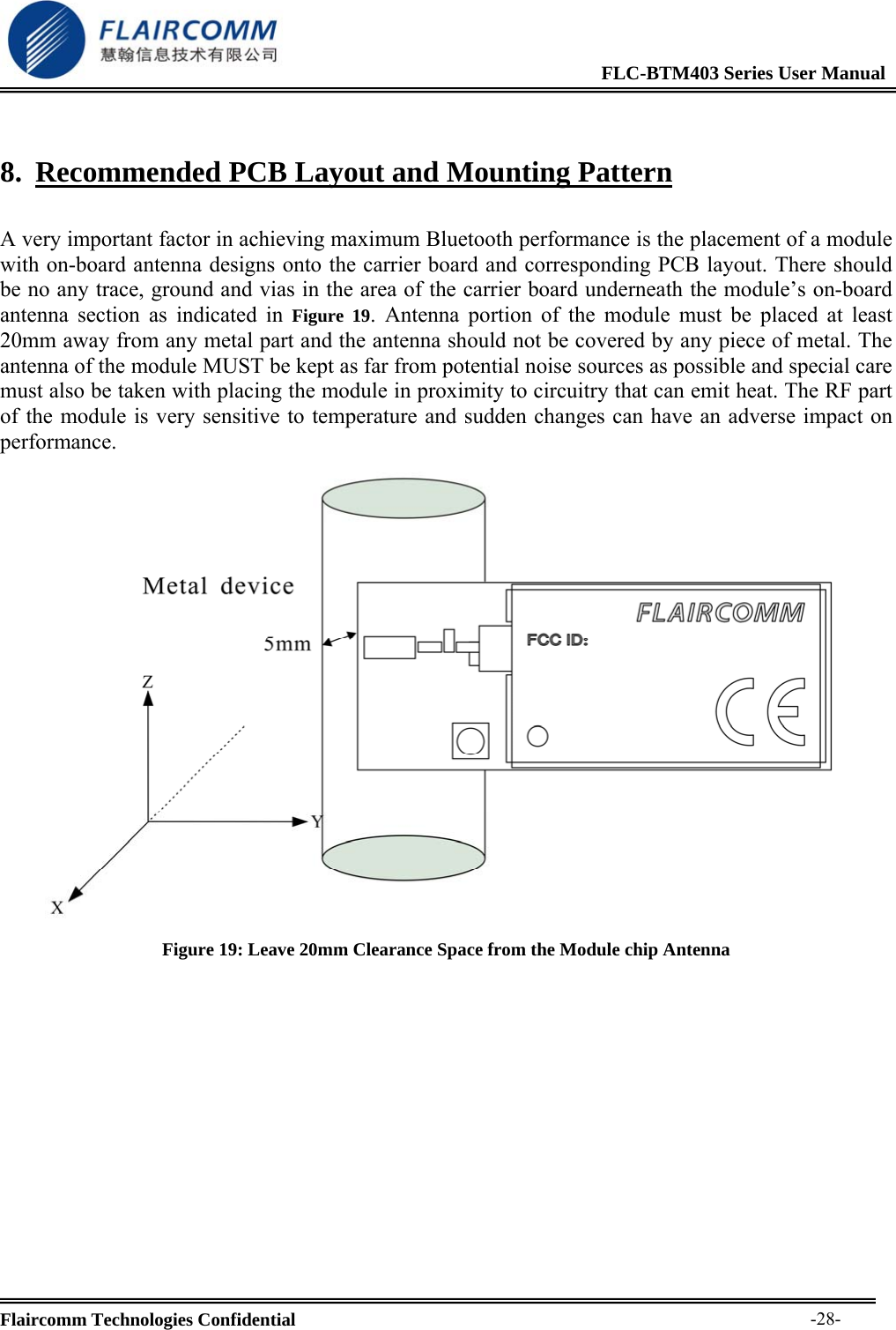
BTM403 User Manual
User Manual
Navigation menu
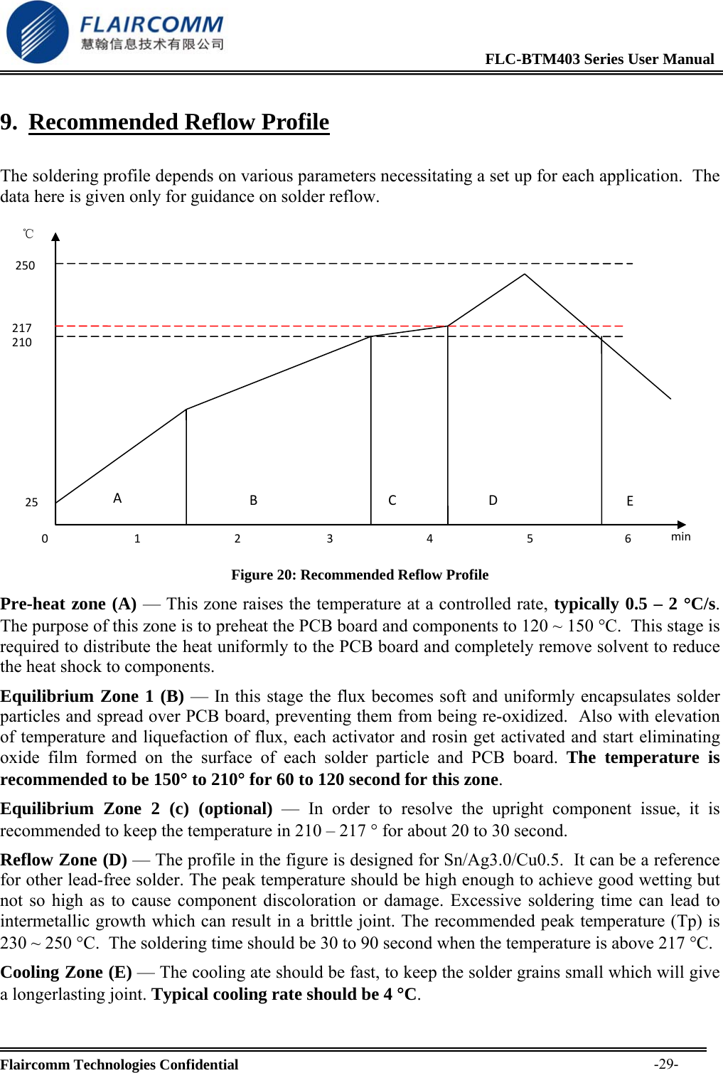
Upload a User Manual
Namespaces
Wiki Guide
HTML
PDF
Info
Views
User Manual
Discussion / Help
Navigation