Fluke Car Amplifier 5220A Users Manual
5220A to the manual 1a0e97f0-0883-44b6-8e1f-568485694fd3
2015-02-02
: Fluke Fluke-Fluke-Car-Amplifier-5220A-Users-Manual-427764 fluke-fluke-car-amplifier-5220a-users-manual-427764 fluke pdf
Open the PDF directly: View PDF ![]() .
.
Page Count: 138 [warning: Documents this large are best viewed by clicking the View PDF Link!]
- 5220A Instruction Manual
- 1. Introduction and Specifications
- 2. Operating Instructions
- 3. Theory of Operation
- 4. Maintenance
- 5. List of Replaceable Parts
- 6. Option and Accessory Information
- 7. Schematic Diagrams

®
5220A
Transconductance Amplifier
Instruction Manual
PN 491936
June 1979 Rev. 3, 6/97
© 1997 Fluke Corporation. All rights reserved. Printed in USA
All product names are trademarks of their respective companies.
LIMITED WARRANTY AND LIMITATION OF LIABILITY
Each Fluke product is warranted to be free from defects in material and workmanship under
normal use and service. The warranty period is one year and begins on the date of shipment.
Parts, product repairs, and services are warranted for 90 days. This warranty extends only to the
original buyer or end-user customer of a Fluke authorized reseller, and does not apply to fuses,
disposable batteries, or to any product which, in Fluke’s opinion, has been misused, altered,
neglected, contaminated, or damaged by accident or abnormal conditions of operation or
handling. Fluke warrants that software will operate substantially in accordance with its functional
specifications for 90 days and that it has been properly recorded on non-defective media. Fluke
does not warrant that software will be error free or operate without interruption.
Fluke authorized resellers shall extend this warranty on new and unused products to end-user
customers only but have no authority to extend a greater or different warranty on behalf of Fluke.
Warranty support is available only if product is purchased through a Fluke authorized sales outlet
or Buyer has paid the applicable international price. Fluke reserves the right to invoice Buyer for
importation costs of repair/replacement parts when product purchased in one country is submitted
for repair in another country.
Fluke’s warranty obligation is limited, at Fluke’s option, to refund of the purchase price, free of
charge repair, or replacement of a defective product which is returned to a Fluke authorized
service center within the warranty period.
To obtain warranty service, contact your nearest Fluke authorized service center to obtain return
authorization information, then send the product to that service center, with a description of the
difficulty, postage and insurance prepaid (FOB Destination). Fluke assumes no risk for damage in
transit. Following warranty repair, the product will be returned to Buyer, transportation prepaid
(FOB Destination). If Fluke determines that failure was caused by neglect, misuse, contamination,
alteration, accident, or abnormal condition of operation or handling, including overvoltage failures
caused by use outside the product’s specified rating, or normal wear and tear of mechanical
components, Fluke will provide an estimate of repair costs and obtain authorization before
commencing the work. Following repair, the product will be returned to the Buyer transportation
prepaid and the Buyer will be billed for the repair and return transportation charges (FOB
Shipping Point).
THIS WARRANTY IS BUYER'S SOLE AND EXCLUSIVE REMEDY AND IS IN LIEU OF ALL
OTHER WARRANTIES, EXPRESS OR IMPLIED, INCLUDING BUT NOT LIMITED TO ANY
IMPLIED WARRANTY OF MERCHANTABILITY OR FITNESS FOR A PARTICULAR PURPOSE.
FLUKE SHALL NOT BE LIABLE FOR ANY SPECIAL, INDIRECT, INCIDENTAL, OR
CONSEQUENTIAL DAMAGES OR LOSSES, INCLUDING LOSS OF DATA, ARISING FROM
ANY CAUSE OR THEORY.
Since some countries or states do not allow limitation of the term of an implied warranty, or
exclusion or limitation of incidental or consequential damages, the limitations and exclusions of
this warranty may not apply to every buyer. If any provision of this Warranty is held invalid or
unenforceable by a court or other decision-maker of competent jurisdiction, such holding will not
affect the validity or enforceability of any other provision.
Fluke Corporation
P.O. Box 9090
Everett, WA 98206-9090
U.S.A.
Fluke Europe B.V.
P.O. Box 1186
5602 BD Eindhoven
The Netherlands
11/99
i
Table of Contents
Section Title Page
1 Introduction and Specifications........................................................ 1-1
1-1. Introduction .......................................................................................... 1-1
1-2. Specifications ....................................................................................... 1-2
2 Operating Instructions....................................................................... 2-1
2-1. Introduction .......................................................................................... 2-1
2-2. Shipping Information............................................................................ 2-1
2-3. Input Power .......................................................................................... 2-1
2-4. Fuse Replacement................................................................................. 2-2
2-5. AC Line Fuse ................................................................................... 2-2
2-6. Power Supply Fuses......................................................................... 2-2
2-7. Rack Installation................................................................................... 2-2
2-8. Operating Features................................................................................ 2-2
2-9. Operating Notes.................................................................................... 2-5
2-10. AC Line Connection ........................................................................ 2-5
2-11. Transconductance Amplifier............................................................ 2-5
2-12. Input Voltage Requirements ............................................................ 2-5
2-13. Input Voltage Selection, Front/Rear ................................................ 2-6
2-14. Current Output, Front/Rear.............................................................. 2-6
2-15. Standby/Operate............................................................................... 2-6
2-16. Local/Remote................................................................................... 2-6
2-17. Status Indicators............................................................................... 2-6
2-18. Audible Output................................................................................. 2-7
2-19. Inductive Loads................................................................................ 2-7
2-20. Operation.............................................................................................. 2-9
3 Theory of Operation........................................................................... 3-1
3-1. Introduction .......................................................................................... 3-1
3-2. Overall Functional Description ............................................................ 3-1
3-3. General............................................................................................. 3-1
3-4. Analog Section................................................................................. 3-1
3-5. Digital Section.................................................................................. 3-4
3-6. Circuit Analysis.................................................................................... 3-4
3-7. Power Supply................................................................................... 3-4

5220A
Instruction Manual
ii
3-8. Preamplifier...................................................................................... 3-6
3-9. A6 Driver ......................................................................................... 3-7
3-10. A7 Output......................................................................................... 3-9
3-11. A8 Analog Control........................................................................... 3-10
3-12. A9 Front Panel ................................................................................. 3-11
3-13. A10 Logic ........................................................................................ 3-11
3-14. Reset Logic .................................................................................. 3-11
3-15. Timing Logic ............................................................................... 3-13
3-16. Standby/Operate Logic ................................................................ 3-14
3-17. Local/Remote Logic .................................................................... 3-15
3-18. Front/Rear Input Logic ................................................................ 3-15
3-19. Failure Status Logic..................................................................... 3-16
3-20. A11 MIS Bus Interface .................................................................... 3-16
4 Maintenance ....................................................................................... 4-1
4-1. Introduction .......................................................................................... 4-1
4-2. Service Information.............................................................................. 4-2
4-3. General Maintenance............................................................................ 4-2
4-4. Cleaning ........................................................................................... 4-2
4-5. Air Filter Maintenance..................................................................... 4-2
4-6. Access Information .......................................................................... 4-2
4-7. Internal Components/Assemblies ................................................ 4-4
4-8. Front Panel Removal ................................................................... 4-4
4-9. A9 Front Panel PCB Removal..................................................... 4-4
4-10. A2 Transformer Assembly Removal ........................................... 4-4
4-11. A6 Driver and A7 Output Assembly Removal............................ 4-5
4-12. A3 Cap Bus Removal .................................................................. 4-5
4-13. A12 Shunt Assembly Removal.................................................... 4-5
4-14. Fuse Replacement ............................................................................ 4-6
4-15. Ac Line Fuse................................................................................ 4-6
4-16. Power Supply Fuses..................................................................... 4-6
4-17. Line Voltage Selection..................................................................... 4-6
4-18. Output Terminal Selection, Front/Rear............................................ 4-7
4-19. Service Tools.................................................................................... 4-8
4-20. Performance Test.................................................................................. 4-8
4-21. Initial Conditions.............................................................................. 4-8
4-22. Front Panel Tests.............................................................................. 4-9
4-23. Zero Output...................................................................................... 4-9
4-24. DC Accuracy and Line Regulation .................................................. 4-10
4-25. Harmonic Distortion......................................................................... 4-10
4-26. Frequency Response......................................................................... 4-11
4-27. Overcurrent Trip Test....................................................................... 4-11
4-28. Overvoltage Trip Test ...................................................................... 4-12
4-29. Calibration Adjustments....................................................................... 4-12
4-30. Initial Conditions.............................................................................. 4-13
4-31. Input Offset Adjustment................................................................... 4-13
4-32. Driver Offset Adjustment................................................................. 4-13
4-33. Output Bias Adjustment................................................................... 4-14
4-34. DC Accuracy Adjustment ................................................................ 4-14
4-35. Frequency Response......................................................................... 4-14
4-36. Overcurrent Adjustment................................................................... 4-15
4-37. Overvoltage Adjustment .................................................................. 4-15
4-38. Replacement of Selected Components ................................................. 4-15
4-39. Resistors R11 and R12..................................................................... 4-16

Contents
(continued)
iii
4-40. Resistor R13..................................................................................... 4-17
4-41. Troubleshooting.................................................................................... 4-18
5 List of Replaceable Parts................................................................... 5-1
5-1. Introduction .......................................................................................... 5-1
5-2. How to Obtain Parts ............................................................................. 5-1
5-3. Manual Status Information................................................................... 5-2
5-4. Newer Instruments................................................................................ 5-2
5-5. Service Centers..................................................................................... 5-2
6 Option and Accessory Information................................................... 6-1
6-1. Introduction .......................................................................................... 6-1
6-2. Accessories........................................................................................... 6-1
6-3. Rack Mounting Kit (M08-205-600)................................................. 6-1
6-4. Rack Slide Kit (M00-280-610) ........................................................ 6-3
6-5. Precision Y5020A Current Shunt..................................................... 6-3
7 Schematic Diagrams.......................................................................... 7-1

5220A
Instruction Manual
iv
v
List of Tables
Table Title Page
1-1. Accessories ............................................................................................................ 1-2
1-2. Specifications......................................................................................................... 1-2
2-1. Controls, Indicators, and Connectors..................................................................... 2-4
3-1. Effect of Reset Command on A10 Logic and A9 Front Panel............................... 3-13
4-1. Required Test Equipment ...................................................................................... 4-1
4-2. DC Accuracy Test.................................................................................................. 4-10
4-3. Frequency Response Test ...................................................................................... 4-11
4-4. Replacement Resistors for R11 and R12 ............................................................... 4-17
4-5. Replacement Resistors for R13.............................................................................. 4-18
4-6. Mainframe and Digital Section Troubleshooting Guide........................................ 4-21
4-7. Analog Section Troubleshooting Guide................................................................. 4-25
5-1. 5220A Final Assembly .......................................................................................... 5-4
5-2. A1 Motherboard PCB Assembly ........................................................................... 5-17
5-3. A2 Power Transformer Assembly ......................................................................... 5-18
5-4. A3 Capacitor Bus PCB Assembly ......................................................................... 5-19
5-5. A4 Regulator PCB Assembly ................................................................................ 5-21
5-6. A5 Preamplifier PCB Assembly............................................................................ 5-23
5-7. A6 Driver PCB Assembly...................................................................................... 5-26
5-8. A7 Output PCB Assembly..................................................................................... 5-28
5-9. A8 Analog Control PCB Assembly....................................................................... 5-31
5-10. A9 Front Panel PCB Assembly.............................................................................. 5-33
5-11. A10 Logic PCB Assembly..................................................................................... 5-34
5-12. A11 MIS Bus Interface PCB Assembly................................................................. 5-36
5-13. A12 Shunt Assembly ............................................................................................. 5-38
5-14. A13 Output Termination PCB Assembly .............................................................. 5-40
5-15. A14 Extender PCB Assembly................................................................................ 5-41

5220A
Instruction Manual
vi
vii
List of Figures
Figure Title Page
5220A Transconductance Amplifier...................................................................... x
1-1. Outline Drawings................................................................................................... 1-5
2-1. Controls, Indicators, and Connectors..................................................................... 2-3
2-2. Maximum Load Inductance vs Frequency............................................................. 2-8
2-3. Typical Transconductance Error for Inductive Loads ........................................... 2-9
3-1. 5220A Functional Block Diagram......................................................................... 3-2
3-2. Transconductance Amplifier Simplified Circuit Diagram..................................... 3-3
3-3. Power Supply Functional Block Diagram ............................................................. 3-5
3-4. A5 Preamplifier Functional Block Diagram.......................................................... 3-6
3-5. A6 Driver Functional Block Diagram.................................................................... 3-8
3-6. A7 Output Functional Block Diagram................................................................... 3-9
3-7. A8 Analog Control Simplified Block Diagram ..................................................... 3-10
3-8. A10 Logic Simplified Block Diagram................................................................... 3-12
3-9. Timing Sequence ................................................................................................... 3-14
3-10. A11 MIS Bus Interface.......................................................................................... 3-18
4-1. Internal Component/Assembly Locations.............................................................. 4-3
4-2. Line Voltage Selection........................................................................................... 4-7
4-3. Test Point Location/Identification ......................................................................... 4-19
4-4. Flowchart Summary of Mainframe and Digital Section Troubleshooting Guide.. 4-20
4-5. Flowchart Summary of Analog Section Troubleshooting Guide........................... 4-24
5-1. 5220A Final Assembly .......................................................................................... 5-8
5-2. A1 Motherboard PCB Assembly ........................................................................... 5-17
5-3. A2 Power Transformer Assembly ......................................................................... 5-18
5-4. A3 Capacitor Bus PCB Assembly ......................................................................... 5-20
5-5. A4 Regulator PCB Assembly ................................................................................ 5-22
5-6. A5 Preamplifier PCB Assembly............................................................................ 5-25
5-7. A6 Driver PCB Assembly...................................................................................... 5-27
5-8. A7 Output PCB Assembly..................................................................................... 5-29
5-9. A8 Analog Control PCB Assembly....................................................................... 5-32
5-10. A9 Front Panel PCB Assembly.............................................................................. 5-33
5-11. A10 Logic PCB Assembly..................................................................................... 5-35
5-12. A11 MIS Bus PCB Assembly................................................................................ 5-37
5-13. A12 Shunt Assembly ............................................................................................. 5-39
5-14. A13 Output Termination PCB ............................................................................... 5-40
5-15. A14 Extender PCB Assembly................................................................................ 5-41

5220A
Instruction Manual
viii
6-1. Rack Mounting Kit ................................................................................................ 6-2
6-2. Rack Slide Kit........................................................................................................ 6-4
7-1. Interconnect Diagram............................................................................................. 7-2
7-2. Chassis Wiring....................................................................................................... 7-4
7-3. Power Supply......................................................................................................... 7-6
7-4. A5 Preamplifier PCB Assembly............................................................................ 7-8
7-5. A6 Driver and A7 Output PCB Assemblies .......................................................... 7-10
7-6. A8 Analog Control PCB Assembly....................................................................... 7-12
7-7. A9 Front Panel PCB Assembly.............................................................................. 7-14
7-8. A10 Logic PCB Assembly..................................................................................... 7-16
7-9. A11 MIS Bus Interface PCB Assembly................................................................. 7-18

Contents
(continued)
ix
5220A
Instruction Manual
x
ajs36f.eps
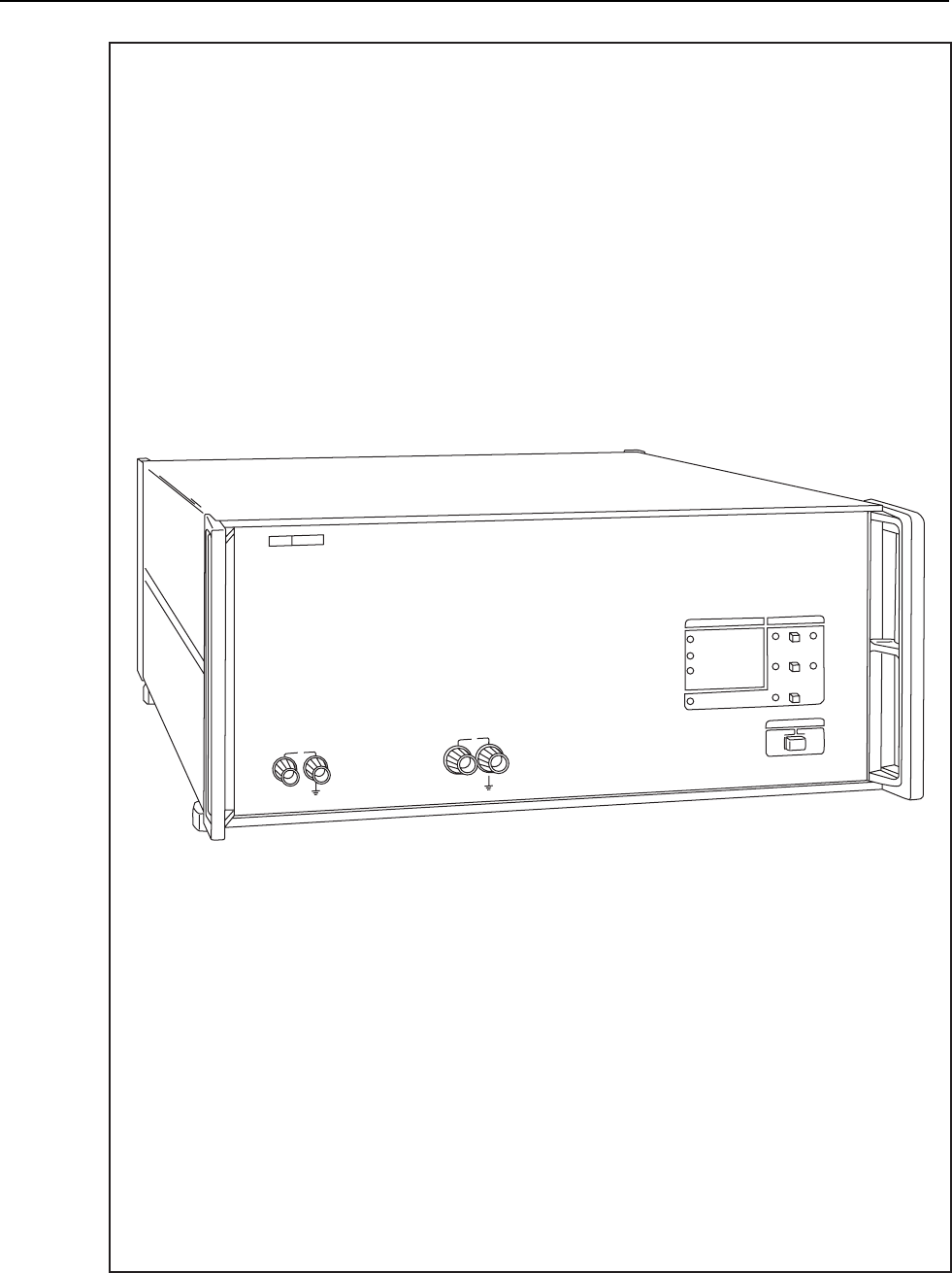
5220A Transconductance Amplifier
1-1
Section 1
Introduction and Specifications
1-1. Introduction
The Model 5220A is a transconductance amplifier designed to operate as either a stand
alone unit or an extension of the Fluke Model 5100 Series Calibrator. Functionally, the
instrument operates as a precision ac/dc current source for calibrating current shunts
and/or current meters. As the name (transconductance amplifier) implies, the output
current level is a function of an input control voltage. The input/output ratio is established
at 1:1 so that a voltage input in the range of -20 to +20 volts will produce a proportional
current output of -20 to +20 amperes. Input voltages may be either dc or ac levels,
depending on the output requirements. Bandwidth for ac operation is dc to 5 kHz.
Control of the 5220A can be handled locally using front panel controls or remotely by
way of the 5100 Series Calibrator. (The 5100 must be equipped with a Model Y5000
Interface.) Control mode selection is accomplished using two front-panel push button
switches, INPUT and LOCAL. The INPUT switch allows selection of either front or rear
control-voltage input connections. The LOCAL switch is used to recall the 5220A from
remote to local operation.
A series of front panel indicators are used to visually display both the control and
operating status of the 5220A. Control indicators include OPER (operate), STDBY
(standby), FRONT input, REAR input, REMOTE, and LOCAL LOCKOUT. The
combination of lit LEDs indicates the present status of the control mode. Status indicators
include THERMAL CUT-OFF, OVER COMPLIANCE, and OVER CURRENT. When
any one of these indicators is lit, an overload condition has been detected causing the
5220A to switch to standby operation. All indicators are active regardless of the selected
control mode, local or remote.
Current output connections are provided on both the front and rear panels. However, only
one set of terminals is active. Selection of the desired set is accomplished internally and
is, therefore, not considered an operator function. Neither local nor remote operation is
affected by the selection of front or rear output.
Forced-air circulation is incorporated in the 5220A to ensure adequate cooling of the
current output stage. Air is pulled in through a rear-panel filter, passed over the output
stage heat sink, and exhausted through the unit’s side panels.
The 5220A is designed to operate from ac line voltages within the range of 90 V ac to
264 V ac, 50 to 60 Hz. One-of-eight specific voltages (100, 110, 115, 120, 200, 220, 230,
240 V ac +10 %) can be selected to ensure compatibility with the local line voltage. The
5220A
Instruction Manual
1-2
selection switches are inside the 5220A. Refer to Section 4 of this manual for information
on how to properly set the line power switches.
Accessories available for use with the 5220A are listed and described in Table 1-1. The
rack mounting kits are designed for use with a standard 19-inch equipment rack. The
Model Y5020A is a precision current shunt recommended for use in calibrating the
5220A. Specify both model number and description when ordering accessories.
Table 1-1. Accessories
Model No. Description
M07-205-600 Rack Mounting Kit
M00-260-610 Rack Slide Kit, 18 in
M00-280-610 Rack Slide Kit, 24 in
Y5020 Precision Shunt
1-2. Specifications
Specifications for the Model 5220A are given in Table 1-2.
Table. 1-2. Specifications
Calibration Cycle All specifications are valid for a 180-day period at an operating
temperature of 20 °C to 30 °C and a relative humidity of 70 % or
less.
Basic
Transconductance 1 Siemen (1 ampere per volt)
Output Range 0 A to 20 A dc or rms ac (28.3 A peak)
Compliance Voltage ≥±4 V dc or 3 V rms ac (4.25 V peak)
DC Accuracy ±(0.025 % of output +1 mA)
AC Accuracy ±(0.05 % of output + 1 mA) from 30 Hz to 1 kHz, and ±(0.05 % of
output + 1 mA) x f from 1 kHz to 5 kHz, where f = frequency in kHz.
Short Term DC Stability Output changes less than ±(0.005 % + 200 µA) in 10 minutes, with
constant line, load, and temperature.
Short Term AC Stability Output changes less than ±(0.01 % + 500 µA) in 10 minutes, with
constant line, load, and temperature.
Harmonic Distortion and Noise ±(0.05 % of output ±1 mA rms) over frequency range of 30 Hz to 1
kHz and measured with a noise bandwidth of 300 kHz, ±(0.05 % of
output + 1 mA) x f from 1 kHz to 5 kHz, where f = frequency in kHz.
Temperature Coefficient ±(0.0025 % of output + 100 µA) per degree C above 30 °C or
below 20 °C.
Transient Recovery Output will settle to within 0.01 % of final value within 2 seconds
following a programmed change in output current or frequency
(10 ms for 5220A alone).

Introduction and Specifications
Specifications
1
1-3
Table 1-2. Specifications (cont.)
Electromagnetic Compatibility This instrument is designed to operate in Standard Laboratory
environments where in electromagnetic environment is highly
controlled. If used in areas with RF fields >0.4 V/m there could be
errors in measurement.
DC Mode (including 5100 Series B)
Output Range ±1 to ±19.9999 A
Accuracy of Output ±(0.025 % of selected output + 1 mA)
Resolution ±0.1 mA
Temperature Coefficient ±(0.003 % of selected output + 100 µA) / °C, above 30 °C and
below 20 °C
Line Regulation Output changes less than 0.001 % for a ±10 % change in line
voltage.
Load Regulation Output changes less than ±(0.005 % + 0.3 mA) for a full load
changes of 4 V of compliance.
AC Mode (including 5100 Series B)
Output Range 1 A rms to 19.9999 A rms
Accuracy of Output ±(0.07 % of selected output + 1 mA rms) from 50 Hz to 1 kHz,
and ±(0.07 % of selected output + 1 mA rms) x f from 1 kHz to 5
kHz, where f = frequency in kHz.
Resolution ±0.1 mA rms
Temperature Coefficient ±(0.003 % of selected output + 100 µA rms) per °C, above 30 °C
and below 20 °C.
Short Term Stability Output changes less than ±(0.02 % + 500 µA rms) in 10 minutes,
with constant line, load, and temperature.
Harmonic Distortion and Noise ±(0.07 % of output + 1 mA rms) over frequency range of 30 Hz to
1 kHz a noise bandwidth of 300 kHz, ±(0.07 % of output + 1 mA)
x f from 1 kHz to 5 kHz, where f = frequency in Hz.
Line Regulation Output changes less than 0.005 % for ±10 % changes in line
voltage.
Load Regulation For frequencies less than 1 kHz:
±(0.005 % lout + 150 µA) per volt of output compliance voltage.
For frequencies greater than 1 kHz:
±(0.005 % lout + 150 µA) x f per volt of output compliance
voltage, where f = frequency in kHz.

5220A
Instruction Manual
1-4
Table 1-2. Specifications (cont.)
General
Load Capability Drives all resistive and capacitive loads consistent with current and
compliance voltage capability. For inductive loads greater than
1 µH and less than maximum inductive loads, output current is
limited to 16 A rms (22.6 A peak)
Maximum Isolation Voltage ±20 V dc or 20 V ac rms
Temperature Range Operating: 0 °C to 50 ° C
Storage: +20 °C to 56 °C
Relative Humidity 50 % to 50 °C, 75 % to 40 °C, 95 % to 25 °C
Altitude Operating: 0 ft to10,000 ft
Non-operating: 0 ft to 40,000 ft
Vibration 2 g maximum, 5 Hz to 55 Hz for 15 minutes
Shock 15 g maximum, half sinewave
Power Requirements 100, 110, 115, 120, 200, 220, 230, or 240 V ac ±10 %, switch-
selectable, 50 Hz to 60 Hz, 300 W
Weight 27 kg (50 lb)
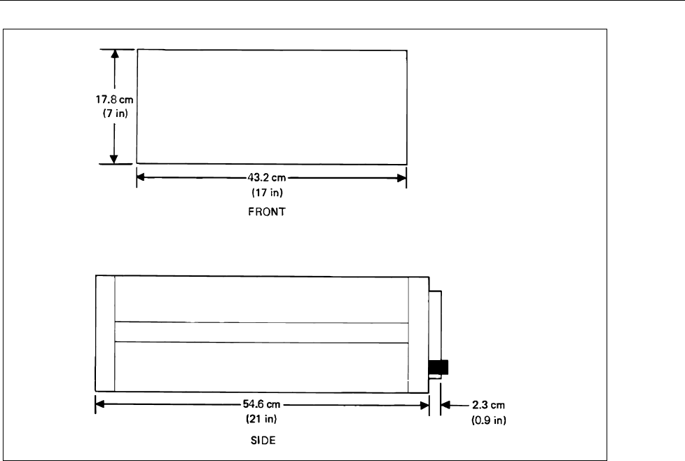
Dimensions 17.8 cm H x 43.2 cm W x 55.9 cm D (7 in H x 17 in W x 22 in D),
case only (See Figure 1-1).
Protection Safety Class 1 Relates solely to insulation or grounding properties as defined in
IEC 348.
Introduction and Specifications
Specifications
1
1-5
ajs01f.wmf
Figure1-1. Outline Drawings

5220A
Instruction Manual
1-6
2-1
Section 2
Operating Instructions
2-1. Introduction
This section of the manual contains information concerning the installation and operation
of the Model 5220A transconductance Amplifier. It is recommended that the contents of
this section be read and understood before any attempt is made to operate the unit. Should
any difficulties arise during operation, contact your nearest John Fluke Sales
representative, or the John Fluke Mfg. Co., Inc., P.O. Box C9090, Everett, WA 98206;
telephone (206) 347-6100.
2-2. Shipping Information
The 5220A is packaged and shipped in a foam-packed container. Upon receipt of the
instrument, a thorough inspection should be made to reveal any possible shipping
damage. Special instructions for inspection and claims are included on the shipping
carton.
If reshipment of the instrument is necessary, the original container should be used. If the
original container is not available, a new container can be obtained from the John Fluke
Mfg. Co., Inc. Please reference the instrument’s model number when requesting a new
shipping container.
2-3. Input Power
The 5220A can be operated from any one of the following 50 to 60 Hz (±1 %) line
voltages: 100, 110, 115, 120, 200, 220, 230, or 240 V ac (±10 %). A rear panel decal
specifies the voltage selected prior to shipment. If a change in voltage is required, refer to
Section 4 of this manual for the selection procedure.

5220A
Instruction Manual
2-2
2-4. Fuse Replacement
2-5. AC Line Fuse
The ac line fuse is accessible by way of a rear-panel fuse holder located to the left of the
input power connector. If fuse replacement is required, disconnect the 5220A from line
power and remove the fuse cap and fuse (twist the fuse cap ccw using a screw driver).
Select and install a replacement fuse whose rating is compatible with the local line
voltage.
1. 100 to 120 V ac use fuse type MDA 3 A
2. 200 to 240 V ac use fuse type MDX 1.5 A
2-6. Power Supply Fuses
Each of the secondary windings on the power transformer is fused to protect the power
supplies from damage in the event of an overload. These fuses, six in all, are internal to
the 5220A and are not available to the operator. Details for replacement by qualified
personnel are given in Section 4 of this manual.
2-7. Rack Installation
The 5220A is designed for either bench-top use or for installation in a standard 19-inch
equipment rack using the accessory Rack Mounting Kit (John Fluke P/N M08-205-600).
Chassis slides (John Fluke P/N M00-280-610) can also be installed to facilitate access to
the instrument when it is installed in an equipment rack. Information regarding the
installation of the rack-mounting accessories is included in Section 6.
2-8. Operating Features
The function and location of all 5220A controls, indicators, and connectors are shown in
Figure 2-1 and described in Table 2-1.
Operating Instructions
Operating Features
2
2-3
ajs02f.wmf
Figure 2-1. Controls, Indicators, and Connectors

5220A
Instruction Manual
2-4
Table 2-1. Controls, Indicators, and Connectors
Ref.
No Name Function
1 STATUS Indicators Three LEDs that light on an individual basis to indicate that the 5220A
has exceeded an operating limit. When the limit condition is detected the
5220A is switched to the standby mode. When the limit condition is
cleared the LED will remain lit until the 5220A is commanded to the
operate mode. The three status conditions are as follows:
THERMAL CUTOFF: Indicates that the output stage of the 5220A has
exceeded its maximum operating temperature.
OVERCOMPLIANCE: Indicates that the compliance voltage at the output
terminals has exceeded its limit.
OVERCURRENT: Indicates that the output current has been
programmed beyond its upper limit.
2 CONTROL Switches
and Indicators
A series of pushbutton switches and LEDs used to select and indicate
the 5220A operating mode. The function of each is as follows:
OPR/STDBY Switch: Allows alternate selection of the standby and
operate modes.
INPUT Switch: Allows alternate selection of the front and rear input
connectors.
REMOTE Switch: Allows recall of the local mode when remote is
enabled and the LOCAL LOCKOUT LED is not lit.
OPR/STBY LEDs: One of the two is lit to indicate the current operating
mode, operate or standby.
FRONT/REAR LEDs: One is lit to indicate the selected voltage input
connector, front or rear.
REMOTE LED: Lights to indicate that the remote mode has been
remotely selected. If the LED is not lit the local mode is enabled.
LOCAL LOCKOUT LED: Lights to indicate that the unit has been
remotely locked in the remote mode. In this event, the three front panel
CONTROL switches are disabled.
3 POWER Switch A push-push switch used to switch instrument power on and off.
4 CURRENT OUTPUT
Terminals (Front)
A pair of banana-jack terminals used to provide front-panel connection to
the output of he current source. The terminals are inactive when the rear-
panel output terminals are selected.
5 VOLTAGE INGUT
Terminals (Front)
A pair of banana-jack terminals that serve as control voltage input
connections in the local/front-input mode.
6 MIS* Bus Connector A 24-pin connector used as an I/O port for remote operation (Fluke MIS
Bus) of the 5220A. When the 5220A is interfaced with a 5100 Series
Calibrator (by way of a Y5000 interface) the 5220A output can be
controlled from the 5100 front panel.
7 Ventilation Filter Prevents dirt and debris from being drawn into the 5220A intake
ventilation port.

Operating Instructions
Operating Notes
2
2-5
Table 2-1. Controls, Indicators, and Connectors (cont.)
Ref.
No Name Function
8 Power Connector Provides the means of connecting the 5220A to ac line power by way of
a 3-wire power cord.
9 Fuse Holder Houses the ac line fuse and allows easy access for fuse replacement.
10 Ground Connector A binding post positioned to provide a convenient connection to chassis
ground.
11 Current Output
Terminals (Rear)
A pair of banana-jack terminals used as rear-panel current output
connections. The terminals are inactive when the front-panel CURRENT
OUTPUT terminals are selected.
2-9. Operating Notes
The following paragraphs describe the various conditions that should be considered
before operating the 5220A.
2-10. AC Line Connection
The rear-panel three-prong, U-ground connector permits the 5220A to be connected,
through a power cord to 50 or 60 Hz line power. The offset prong on this connector is
connected to the 5220A chassis and should be connected, via the power cord, to a high-
quality earth ground.
2-11. Transconductance Amplifier
A transconductance amplifier is a current source whose output current level is
proportional to an analog input voltage. Electrically, the output of the unit appears as a
constant current source with an output impedance that is much greater than the load
resistance. Similarly, its input impedance is much greater than that of the input voltage
source.
The input/output ratio of the 5220A is 1:1, and the output current range is +20 to –20 A.
Therefore, the range of the input control voltage is +20 to –20 V dc. The compliance
voltage of the 5220A is 3 V rms ac or +4 V dc.
2-12. Input Voltage Requirements
Input control voltage for the 5220A can be supplied by any low-impedance voltage
source with an output proportional to the desired output current. The source may be either
ac (30 Hz to 1 kHz) or dc, fixed or adjustable, depending upon the output requirements.
The control voltage source may be connected to either the front-panel VOLTAGE
INPUT terminals or the rear-panel voltage input terminals (Pins 5 (low) and 6 (high) of
the 24-pin connector), but not both simultaneously. Instrument damage will not result
from the simultaneous connection of two sources. However, interaction between the two
inputs can result in source loading, which in turn can cause inaccuracy in the expected
current output level.
If a rear-panel input is desirable, the use of the 5100 Series Calibrator and a Y5000
Interface is recommended. This combination allows the 5220A to be operated remotely
as an extension of the 5100. If the use of an alternate rear-input source is desirable, the
user is responsible for the proper interface. Details for custom interface requirements can
be derived from the theory of operation (Section 3) and the detailed schematics (Section
8).

5220A
Instruction Manual
2-6
2-13. Input Voltage Selection, Front/Rear
Selection of the front or rear terminals for control voltage input is manually accomplished
by pressing the INPUT push button switch on the front panel. Each depression alternately
selects front or rear as indicated by the lit FRONT/REAR LED indicator. This switch is
active in the local mode, and inactive in the remote mode.
2-14. Current Output, Front/Rear
The 5220A current output can be taken from either a front- or rear-panel set of five-way
binding post terminals, but not both simultaneously. An internal jumper configuration
allows qualified personnel to establish the desired output. A detailed output selection
procedure is given in Section 4, Maintenance.
2-15. Standby/Operate
When the 5220A is energized it can be placed into one-of-two operating modes; standby
or operate. The enabled mode is indicated by a lit front panel LED; OPR (operate) or
STDBY (standby). Standby is essentially a reset state, in which the output of the
transconductance amplifier is forced to zero regardless of the input control voltage level.
In the standby mode both the amplifier and the device connected to its output are
protected from accidental overloads. The operate mode is enabled when an output is
required. It causes the amplifier to respond to the control voltage input, and thereby
provides the appropriate current level output.
A front panel pushbutton switch (located between the OPR/STDBY LEDs) allows
manual selection of either mode when the LOCAL LOCKOUT LED is not lit. However,
the selection can be counteracted under certain conditions. For example, either mode may
be remotely selected, and the detection of an output overload will command the standby
mode. Similarly, when the unit is initially energized it is forced to standby.
2-16. Local/Remote
The 5220A can be operated manually using the front panel controls, or remotely by way
of the rear panel connector. When the unit is initially energized, it is forced to the local
control mode (REMOTE LED is not lit). The remote mode can only be selected by way
of a remote control source. When remote is enabled (REMOTE LED is lit) the local
mode can be recalled by a remote command or by pressing the LOCAL push-button
switch on the front panel. However, if the LOCAL LOCKOUT is lit (this is also a remote
command) the local mode can only be recalled by a remote command.
2-17. Status Indicators
A series of three front-panel STATUS LEDs provide a visual indication of overload
conditions that have been detected at the 5220A output. They are: THERMAL CUTOFF,
OVERCOMPLIANCE, and OVERCURRENT. When any one of these conditions is
detected the appropriate LED is lit and the unit is commanded to standby. The LED will
remain lit even after the overload condition has been relieved. To return the unit to the
operate mode the overload must be cleared and the operate mode must be commanded. If
operate is commanded while the overload is still present, the unit will remain in standby.
A thermal cutoff indication identifies overheating of the current output stage. If the
heating is excessive a cooling-down period may be required before the condition is
cleared.
The presence of an open-circuit or a high impedance load at the output terminals will
cause an overcompliance indication. In this case, an appropriate load will have to be

Operating Instructions
Operating Notes
2
2-7
connected to the output before the condition can be cleared. Overcompliance is detected
as an output voltage outside the range of +4 V dc or 3 V rms ac.
Output current in excess of 20 A will cause an overcurrent indication. To correct the
condition, the input control voltage must be reduced to an acceptable level.
2-18. Audible Output
When the 5220A is used to output high current at high frequencies (above 10 A and 1
kHz) it may emit an audible tone. The sound is normal and is characteristic of power
transistors that are operated at high current density. Several factors will cause the sound
to be more or less apparent. They include background noise, location of the 5220A
relative to the operator, and operator’s hearing ability.
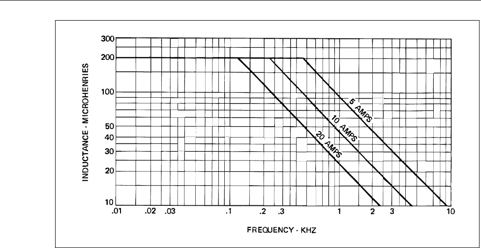
2-19. Inductive Loads
The 5220A will drive an inductive load of up to 200 µH. However, reasonable care must
be exercised to ensure the desired results. One or more of the following considerations
may apply to a given application:
1. Compliance voltage (3.0 V maximum) places a restriction on the product of
inductance and operating frequency for a given output current. This is illustrated in
Figure 2-2 for maximum load inductance vs frequency at output currents of 5, 10,
and 20 A.
2. A step change in output current into an inductive load can easily produce an
overcompliance condition. If the control voltage is being input at the front panel
terminals, the rate of change must be controlled to avoid an overcompliance trip. An
alternate approach is to set the 5220A to standby before making a change in the
control voltage, then select the operate mode. This allows the 5220A to internally
control the rate of change. If the control voltage is taken from a Fluke Model 5100
Series Calibrator, the calibrator will limit its output to an acceptable rate of change.
3. The leads used to connect a load to the 5220A can add appreciably to load
inductance. For example, a pair of 5-foot leads (10 feet of wire) made of 18 gauge
wire (AWG) will have a calculated inductance of 3.86 µH. This is enough to cause an
overcompliance trip if a step change in the input control voltage occurs.
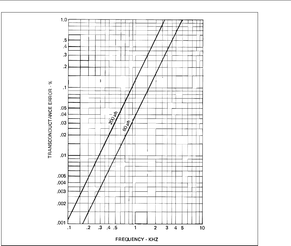
4. When driving an ac current through an inductive load the 5220A will exhibit
increased distortion and transconductance error. This is due to a reduction in loop
gain caused by the inductance. The graph in Figure 2-3 illustrates the typical
transconductance error, as a function of frequency, for two different inductive load
values.
5220A
Instruction Manual
2-8
ajs03f.wmf
Figure 2-2. Maximum Load Inductance vs Frequency
Operating Instructions
Operation
2
2-9
ajs04f.wmf
Figure 2-3. Typical Transconductance Error for Inductive Loads
2-20. Operation
The following procedure is suggested for operating the 5220A. With reference to the
previous paragraphs proceed as follows:
1. Connect the 5220A to the 5100 Series Calibrator via the Y5000 Interface if remote
operation is desired. See the 5100B/Y5000 Instruction Manuals for details.
2. Connect the 5220A to line power.
3. Turn-on the 5220A by depressing the POWER switch to the ON position. Only the
STDBY and FRONT indicators should be lit.
4. Energize peripheral equipment as required.
5. If local operation is required, connect the control voltage source to the front-panel
VOLTAGE INPUT terminals.
6. Adjust the output of the control voltage source (remote or local) to approximately
1 V.

5220A
Instruction Manual
2-10
7. Determine the active output terminals (front or rear) by connecting a short jumper
wire between the front-panel CURRENT OUTPUT terminals and then pressing the
OPR/STDBY switch. If the OVERCOMPLIANCE LED lights, the rear output
terminals are active. Otherwise, the OPR LED will light indicating that the front
CURRENT OUTPUT terminals are active.
8. Press the STDBY switch and then remove the short from the front output terminals.
9. Connect the intended load between the active output terminals.
10. Adjust the control voltage to the desired level.
11. Command the operate mode. If the OPR LED is lit, the predetermined current level is
flowing through the load.
12. Set the unit to standby before disconnecting the load or setting the POWER switch to
OFF.
3-1
Section 3
Theory of Operation
3-1. Introduction
This section of the manual contains an overall functional description followed by a
detailed circuit analysis of the 5220A. Both descriptions are supported by block
diagrams. Component level descriptions contained in the circuit analysis are referenced to
the detailed schematics in Section 8 of this manual.
3-2. Overall Functional Description
3-3. General
The 5220A is a transconductance amplifier. That is, a current source whose output
current is proportional to an analog input voltage. Electrically viewed at the output
terminals, the 5220A appears as a current source with an output impedance that is very
much greater than the load resistance. Its input terminals exhibit a similar characteristic;
the input impedance is larger than that of the input voltage source.
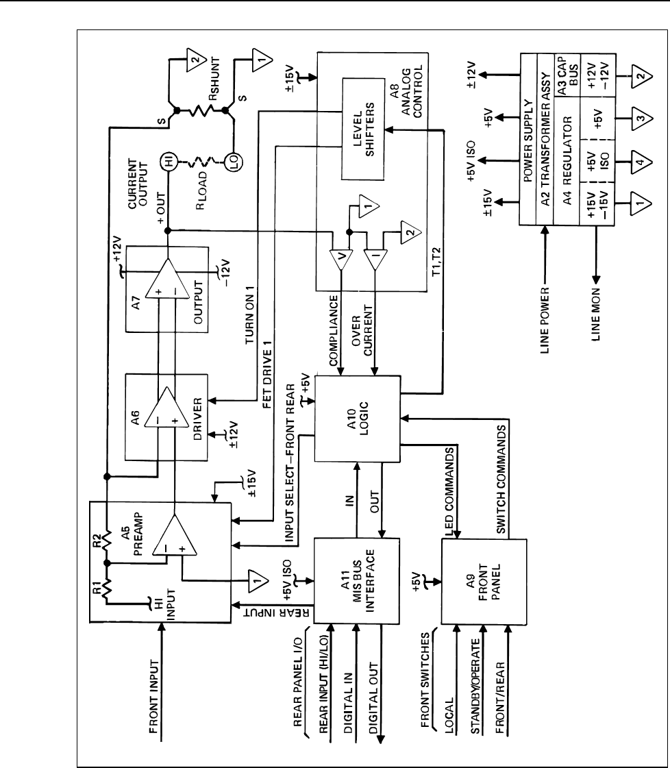
Functionally, the 5220A, as shown in Figure 3-1, can be divided into two sections, analog
and digital. The analog section consists of the power supplies, the transconductance
amplifier, and associated analog control circuitry. The digital section comprises the logic
necessary for overall control, and the interfaces necessary for front panel (local)
operation and remote operation by way of the Fluke MIS Bus.
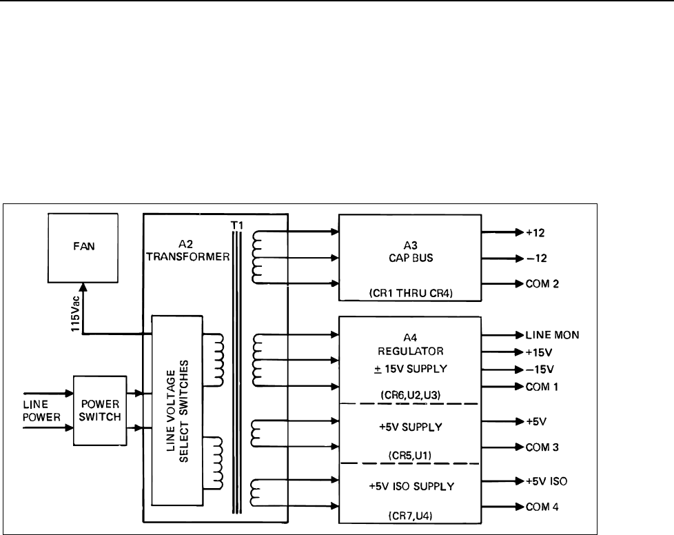
3-4. Analog Section
The power supply used in the 5220A provides operating voltages for both the analog and
the digital section of the unit. It consists of three separate assemblies: the A2 Transformer
Assembly, the A3 Cap Bus, and the A4 Regulator. The Cap Bus and Regulator
Assemblies comprise the output portion of the supply, while the Transformer Assembly
provides isolated ac power for the power supplies. Regulated supply voltages are a
function of the A4 Regulator. These include +5 V dc and +5 V dc Isolated for the digital
circuits and +15/-15 V dc for analog circuit operation. Unregulated voltages are a
function of the A3 Cap Bus. The Cap Bus is a high-current, +12/-12 V dc source for the
5220A current output.
5220A
Instruction Manual
3-2
ajs05f.wmf
Figure 3-1. 5220A Functional Block Diagram
Theory of Operation
Overall Functional Description
3
3-3
The transconductance amplifier is a three-stage, closed-loop amplifier whose feedback
signal is proportional to the 5220A output (load) current. It consists of the A5 Preamp,
the A6 Driver, the A7 Output, and a precision four-terminal shunt. Input voltage to the
amplifier is presented, by way of front or rear input terminals, to the A5 Preamp. This
assembly includes relays for front/rear input selection, precision feedback resistors to
establish overall loop gain, and a high-gain amplifier equipped with on/off control for
power-on/off sequencing and failure control. The output of the A5 Preamp is input
directly to the A6 Driver where it is buffered and passed on as a differential input to the
high-current A7 Output stage. Output current from this stage is returned through the
output load and a precision current shunt to power supply common (COM 2) of the A3
Cap Bus (high-current supply). The voltage drop that occurs across the shunt is sent to
the A5 Preamp as a feedback signal, thus closing the loop.
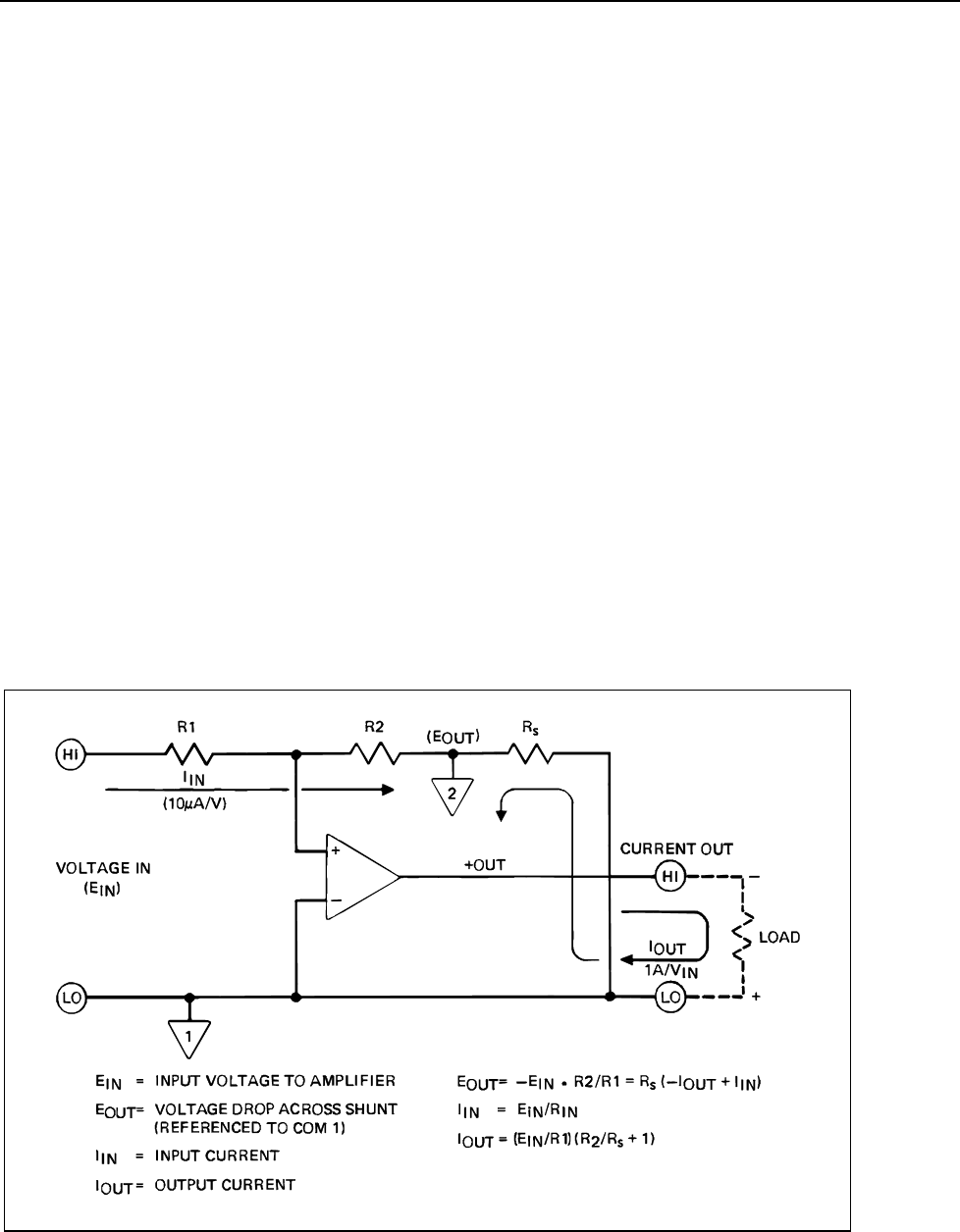
Overall operation of the transconductance amplifier is illustrated in Figure 3-2. When an
input voltage, EIN, is applied to the amplifier an output current, IOUT, is produced. The
current passes through the series connected load and the precision shunt, RS. Current
passing through the shunt produces a voltage (IR) drop, EOUT, whose polarity (with
respect to COM 1) is opposite that of the input voltage. This voltage is returned to the
amplifier as negative feedback through resistor R2. The values of R1, R2 and RS
established the 1:1 ratio of input voltage to output current. See equations in Figure 3-2.
The analog control circuit constantly monitors the voltage and current outputs of the
transconductance amplifier and provides overcompliance and overcurrent indications to
the digital section of the 5220A. When an overload condition occurs, the digital section
responds by sending shut-down signals to the amplifier by way of the analog control
logic. Control sequencing signals (T1, T2) for amplifier turn-on are also processed by the
analog control circuit.
ajs07f.wmf
Figure 3-2. Transconductance Amplifier Simplified Circuit Diagram

5220A
Instruction Manual
3-4
3-5. Digital Section
The logic portion of the 5220A controls the sequencing of input relays (front/rear) and
other control signals that turn the transconductance amplifier on and off. It also provides
drive commands to light appropriate front panel status LEDs. Inputs to the logic are in the
form of local/remote control commands from the front panel switches or the remote MIS
Bus Interface, and overload signals from the analog control circuit.
Local or front panel control of the 5220A is accomplished through a series of front panel
pushbutton switches which provide direct inputs to the logic circuit. Control and/or status
responses to the commands are displayed on the front panel LEDs.
Remote control of the 5220A is enabled by the A11 MIS Bus Interface. The interface is
intended for use with a 5100 Series Calibrator equipped with a Y5000 Interface. Control
data (analog and digital) is received at the A11 MIS Bus Interface by way of a connector
on the rear panel of the 5220A. In the remote mode, this data is processed by the interface
and internally coupled with the analog and digital sections of the 5220A.
3-6. Circuit Analysis
A detailed circuit description of the 5220A is given in the following paragraphs. The
description is keyed to the functional blocks defined in Figure 3-1. Each block is
described separately and is supported by both a block diagram and a detailed schematic
diagram (see Section 8 for schematics).
3-7. Power Supply
The power supply, as shown in Figure 3-3, consists of the three major assemblies: A2
Transformer, A3 Cap Bus, and A4 Regulator. Its function is to transform line power into
four sets of 5220A operating voltages. Each voltage set is isolated from the other, and
three of the four are regulated. The three regulated voltage sets are +15/-15 V dc,
+5 V dc, and +5 V ISO (isolated). The unregulated voltage set is +12/-12 V dc.
The A2 Transformer assembly consists of a series of three line-voltage selection
switches, a power transformer, and appropriate secondary output fuses. Line power to the
transformer passes through the front panel power switch (S4) and the line voltage
selection switches before reaching the two primary windings. The setting of the line
voltage switches (S1) connects the primary windings in either a parallel or a series
configuration. Parallel connection is required for 115 V ac operation and the series
connection is used for 230 V ac. Switches S2 and S3 allow selection of alternate primary
winding taps. They allow operation from 100, 110, 115 or 120 V ac line voltages in the
parallel configuration, or from 200, 220, 230 or 240 V ac in the series configuration. The
115 V ac ventilation fan is permanently connected to one of the primary windings, thus
ensuring proper operation in either voltage configuration. Fuse protection for the power
line is provided by an external fuse (F1) mounted on the rear panel. Supply overload
protection for the regulated supplies is provided by secondary-winding fuses F4, F5, F6,
and F7 located on the A2 Transformer Assembly.
The A3 Cap Bus is a high-current, unregulated, +12/-12 V dc power supply designed to
provide operating power to the output amplifier. It consists of two fuses, a full-wave
rectifier, two bleeder resistors, and a bank of filter capacitors. Operating voltage is
derived from a high-current center-tapped secondary winding of T1. It enters the A3 Cap
Bus through overload fuses F2 and F3, and is full-wave rectified by diodes CR1 through
CR4 to establish both positive and negative supply voltages. Filter capacitors, C1 through
C8, filter the supply outputs. Bleeder resistors, R2 and R3, discharge the filter capacitors
when line power is turned off.
Theory of Operation
Circuit Analysis
3
3-5
The A4 Regulator is designed to convert the ac outputs from the three remaining
secondary windings of T1 into three sets of isolated and regulated voltages: +5 V dc,
+15/-15 V dc, and +5 V dc ISO (isolated). Each voltage is produced using conventional
regulating techniques. That is, it is rectified, filtered, regulated by a three-terminal
regulator, and filtered again before being output. A fifth voltage, Line Mon (monitor), is
also produced on the A4 Regulator. It is derived from the T1 windings used for the
+15/-15 V dc supply and is used to convey the line power status of the 5220A to the A10
Logic. The voltage is rectified by diodes CR8 and CR9, and clipped by zener VR1 before
being output.
ajs08f.wmf
Figure 3-3. Power Supply Functional Block Diagram
5220A
Instruction Manual
3-6
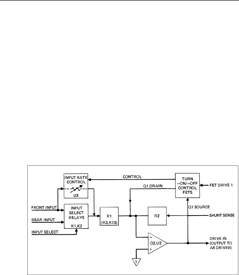
3-8. Preamplifier
The A5 Preamplifier, as shown in Figure 3-4, is a high-gain amplifier designed to accept
a front/rear panel input signal and provide an amplified output to the A6 Driver stage of
the transconductance amplifier. It consists of a high-gain differential amplifier with
feedback resistors, front/rear input select relays, and turn-on/off control circuitry.
In operation, the input voltage source (front or rear), as selected by the A10 Logic, is
connected through reed relay K1 (front) or K2 (rear) and input resistors R1, R3, and R13
to the inverting input of a differential transistor pair, Q2. The non-inverting input of Q2 is
connected to COM 1 through parallel resistors R9 and R14. The resistance value
approximates the value of R1 and R2 in parallel and, thereby balances the source
impedance at the amplifier inputs. Balance is required to minimize apparent input offset
voltage that may result from input currents. Diode CR3 and diode-connected transistor
Q3 are voltage clamps that prevent amplifier saturation on high input transients. The
collectors of Q2A and Q2B drive the emitters of a pair of grounded base amplifiers
formed by transistor array, U1. This holds the collectors of Q2 at a low and equal level to
maintain low and equal collector-to-base leakage currents (ICER) at Q2. The actual
collector voltage of Q2 is set by the temperature corrected divider formed by R4, R19,
and the diode connected transistor U1C. Voltage variations at the collectors of U1A and
U1B constitute the output of the differential amplifier, and are used as the input to op-
amp, U2. Diodes CR4 and CR5 clamp the inputs to prevent U2 saturation when transient
voltages appear. An ac feedback network, R15 and C7, fix the frequency response of the
preamplifier to satisfy the overall transconductance amplifier loop. Amplifier zero is
established by the selected values of collector resistors R11 and R12, and the setting of
the zero-adjust potentiometer, R6.
ajs09f.wmf
Figure 3-4. A5 Preamplifier Functional Block Diagram
The turn-on/off control FET (Q1) operates as FET switch to control the overall gain of
the A5 Preamplifier in both the standby and operate modes. Q1 responds to the FET
Drive 1 signal initiated (as T2) on the A10 Logic.
In the standby mode FET Drive 1 is near zero volts causing Q1 to turn on. FET Q1
completes the feedback loop between the output of U2 and the inverting input of Q2. This
in effect reduces the gain of the A5 Preamplifier to zero. As a result the output of the
transconductance amplifier is forced to zero amperes. Photo resistor U3 is used to control

Theory of Operation
Circuit Analysis
3
3-7
the rate at which the input voltage is applied to the A5 Preamplifier when the 5220A is
switched from standby to operate. This is necessary to prevent a step output which, if
applied to an inductive load, would result in an overvoltage transient, forcing the 5220A
back to standby. In standby both input select relays, K1 and K2, are open, capacitors, C3
and C12, are discharged, and the photo resistor U3 is a very high impedance with the
LED drive removed. Thus, the A5 Preamplifier is effectively isolated from the input
voltage.
In the operate mode FET Drive 1 is stepped to –15 V dc causing FET Q1 to turn off.
With Q1 off, the A5 Preamplifier returns to its high gain state with feedback established
by resistors R1 and R2. If front input is selected, the Relay 1 drive signal is low and
capacitor C12 begins charging. The increasing voltage across C12 increased the LED
output from U3 which, in turn, decreases the impedance of the photo resistor. Since the
resistor is in parallel with the input contacts of the still open front input relay K1, it acts
as a variable input attenuator. In other words, the front input voltage is applied to the
input of the A5 Preamplifier at a controlled rate and not as a step input. At the same time,
a low Relay 1 drive signal is inverted by U4 causing C3 to charge through R24. When the
charge reaches the threshold of the second inverter (U4) relay K1 is energized by a set of
four parallel connected inverters. The charge time for C3 and C12 are designed to ensure
that K1 closes after photo resister U3 changes to a low impedance. When K1 closes, it
places a short across the resistor in U3 and selects the front panel input voltage to drive
the A5 Preamplifier. If the rear panel input signal is selected, a variable attenuator is not
necessary because the signal from the remote 5100A rises at a controlled rate when
switched from standby to operate.
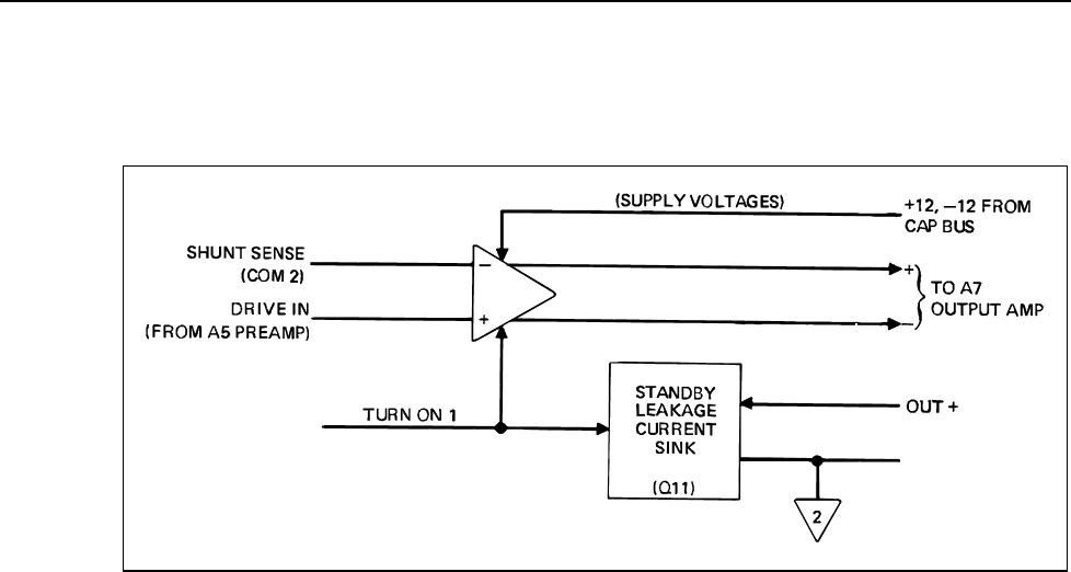
3-9. A6 Driver
The A6 Diver, as shown in Figure 3-5, is a differential amplifier designed to accept its
input from the A5 Preamplifier and to provide a differential drive signal to the A7 Output
stage. The amplifier itself is of a discrete-component, complementary, push-pull design.
Its features include the following:
• Temperature compensated biasing for both itself and the A7 Output stage
• An amplifier-disable circuit for standby operation
• An output-leakage current sink for standby operation.
The input section of the driver amplifier consists of a differential transistor pair, Q2 and
Q3; a current regulator, Q4; and a common base driver, Q1, for the bias circuit.
Transistor Q3 of the input pair receives the drive input from the A5 Preamplifier. The
other input transistor, Q2, is driven by Shunt Sense 2, which provides negative feedback
from the output current shunt to reduce distortion in the A7 Output stage. Current
regulator Q4 regulates the emitter current of the differential pair, and provides isolation
from variations in the –12 V supply. Output from the differential pair is taken at the
collector of Q3 by way of a common-base driver, Q1.
The bias section of the driver amplifier consists of resistors, R13 through R17, current
regulator, CR1, and transistors, Q5 and Q107 (Q107 is physically located on the output
amplifier's heat sink). Resistors R13 through R17 and current regulator CR1 form a series
string that is driven by the output driver Q1 of the input amplifier. Regulator CR1 is at
the end of the string and connected to –12 V dc. This ensures a constant current of
approximately 5.2 mA through the string. Transistors Q5 and Q107 are connected across
resistors R14, R15 and R16, R17 as VBE multipliers to ensure that the voltage drop
across the resistor string changes at a rate which will compensate for VBE temperature
changes in the A6 Driver and A7 Output stages. Transistor Q5 senses ambient
temperature changes while Q107 senses temperature changes due to power dissipation in
the A7 output. The temperature compensated voltage drop developed across the resistor
5220A
Instruction Manual
3-8
string is used as a voltage source to set the quiescent bias for the remaining stages of the
complementary A7 Driver and A7 Output. Variable resistor R13 is used to set the initial
bias voltage.
ajs10f.wmf
Figure 3-5. A6 Driver Functional Block Diagram
The characteristics of the VBE multipliers used in the bias section are stated in terms of
Q5 in the following formulas:
VBE = [R14/R14 + R15] VCE
VCE = VBE [R14 + R15/R14]
The output section of the A6 Driver consists of transistors Q8, Q9, Q10, Q12, and
associated components. Transistors Q8 and Q9 are arranged as complementary emitter
followers that are both biased and driven by the bias section. This is followed by a
common collector stage using Q10 and Q12. Overcurrent protection is provided in the
stage by the 10 ohms resistors, R30 and R31, in the collector circuits. The differential
output at the emitters of Q10 and Q12 is used as the drive input to the A7 output stage.
In the standby mode of operation it is necessary to reduce the 5220A output to a zero-
volt/zero-current condition. This is accomplished on the A6 Driver by two separate FET
circuits. FETs Q6 and Q7 comprise the voltage shut-down circuit, and FET Q11 is the
output current-sink. Both are enabled by a Turn-on 1 signal which is initiated (as T1) by
the A10 Logic when the 5220A is switched to standby. When Q6 and Q7 are enabled
(turned on) they remove the bias from the output stage of the A6 Driver, and thereby
disable the bias to the A7 Output stage. In this state the output is essentially floating and
is influenced only by leakage current that may be present in the output drivers. FET Q11
remedies the floating condition by effectively clamping the output to output common
(COM 2).
Theory of Operation
Circuit Analysis
3
3-9
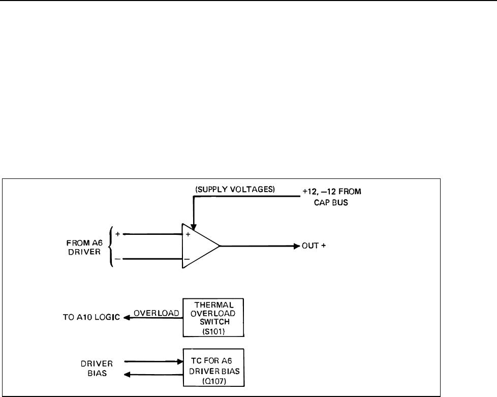
3-10. A7 Output
The A7 Output is a discrete-component, complementary-output, high-current amplifier
which serves as the final output stage of the transconductance amplifier. See Figure 3-6.
It consists of a pair of driver transistors, Q101 and Q102; two parallel pair(s) of output
transistors, Q103, Q104 and Q105, Q106; a thermal sensing transistor, Q107; and a
thermal overload switch S101. The differential output from the A6 Driver is applied to
the bases of Q101 and Q102. These transistors are configured as emitter followers and
provide the high current drive required by the output transistors. Collector resistors, R114
and R115, for Q101 and Q102 provide current limit protection under transient or fault
conditions. Emitter resistors in the parallel output pairs prevent current hogging which
would otherwise occur due to unequal VBE characteristics.
ajs11f.wmf
Figure 3-6. A7 Output Functional Block Diagram
All transistors in the A7 Output as well as the thermostatic switch, S101, are physically
mounted on a common heat sink. The temperature of the heat sink is sensed by Q107
(part of the A7 Driver’s bias network) and returned to the A7 Driver to provide bias
compensation for the change in VBE with output-transistor temperature. (See A7 Driver
description given earlier in this section of the manual.) Thermostatic switch S101 senses
the temperature of the heat sink and provides an open contact output when an over-
temperature condition is detected. The open output is sent to the A10 Logic which reacts
by switching the 5220A to standby (over temperature may result from a loss or restriction
of cooling airflow).
5220A
Instruction Manual
3-10
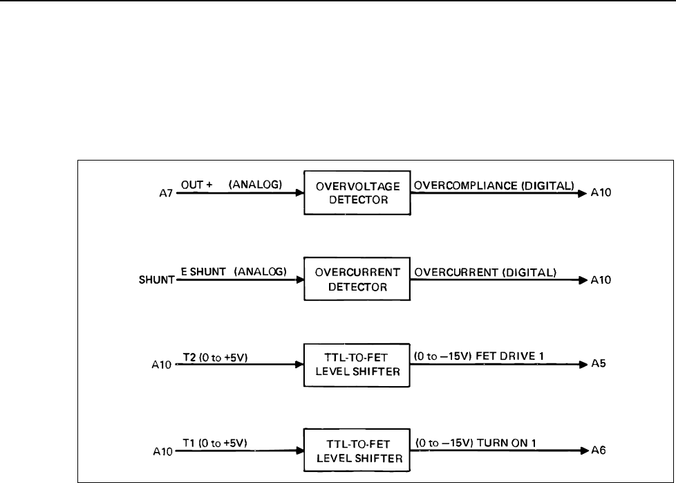
3-11. A8 Analog Control
The A8 Analog Control Assembly, as shown in Figure 3-7, contains an overcompliance
detector, an overcurrent detector and two TTL-to-FET level shifters. The detection
circuits are used to switch the 5220A to standby when an overcurrent or overcompliance
condition occurs. The level shifters are driven by the A10 Logic to control the turn-on/off
sequencing of the transconductance amplifier.
ajs12f.wmf
Figure 3-7. A8 Analog Control Simplified Block Diagram
The detection circuits are absolute value level detectors that provide a TTL output
indication of the transconductance amplifier’s operating status; i.e., output voltage status
and output current status. As long as both output voltage and current are within their
specified operating range, both detectors will output a low logic level as a normal-
operation status indication. However, if either or both the specified compliance voltage
and/or the output current are exceeded, the appropriate detector will output a high logic
level. Upon receipt of a high logic level from either detector the A10 Logic switches the
5220A to standby.
Each of the detectors is basically the same. They consist of an absolute value amplifier
(full-wave rectifier), a level conditioner, a zener diode threshold detector, and a TTL
buffered output stage. The absolute value amplifier is essentially a pair of operational
amplifiers configured to provide an output voltage that is equal to the amplified positive
absolute value of the input signal. The input to the compliance detector is connected to
sense the voltage present at the output terminals (+OUT and COM 1). Similarly, the input
to the overcurrent detector is connected to sense the voltage drop across the current shunt
(COM 2 and COM 1). The result, in both cases, is a negative output level that is equal to
the absolute value of the input signal. This level is sent to a level conditioner where it is
filtered/integrated, inverted, and amplified. An adjustable gain control in the level
conditioner’s feedback loop provides for accurate adjustment of the trip level.
The output of the level conditioner feeds a series connected zener/resistor circuit with the
resistor connected to logic common (COM 3). When the output of the level conditioner
exceeds the zener voltage, the excess is dropped across the zener resistor. This voltage is
monitored by a series-connected-pair of inverters which respond to the voltage drop as if

Theory of Operation
Circuit Analysis
3
3-11
it were a logic level. That is, voltages from 0 to an approximate 2 V threshold are
considered a low logic level. A high logic level is approximately 2 to 4.5 V.
The TTL-to-FET level shifters are used to interface turn on/off commands TTL logic
levels, T1 and T2, from the A10 Logic with the standby/operate control FETs in the
transconductance amplifier. Both level shifters are identical in design. The input is
designed to respond to voltage levels from +0.01 to +5.0 V dc. Corresponding output
levels to drive the FET gates are 0 to –15 V dc.
3-12. A9 Front Panel
The A9 Front Panel Assembly contains the switches (with the exception of the power
switch) and LEDs that comprise the 5220A controls and indicators. The switches are used
to manually convey control information to the A10 Logic. This includes selection of the
local operating mode, standby/operate, and front/rear panel input. The LEDs display the
current operating status of the 5220A as determined by the A10 Logic. Status conditions
include: remote, local lockout (LLO), overcompliance, overcurrent, thermal cutout, front
panel input, rear panel input, standby, and operate.
Electrically, the LEDs (anode end) and the switches (arm) are connected to a common +5
V bus powered by the logic supply. A switch depression represents a +5 V output to the
A10 Logic. A series resistor connected to the anode end of each LED serves as a current
limiter when the LED is lit. A low logic level from the A10 Logic lights the appropriate
LEDs.
3-13. A10 Logic
The A10 Logic, as shown in Figure 3-8, is designed to process and control the timing and
the input/output of all 5220A digital control data. Input data is received from the front
panel controls, the A11 MIS Bus Interface, and the analog protection circuits of the
transconductance amplifier. Output data provides timing and control signals to the
amplifier (including its relays) and the front panel indicator LEDs.
3-14. Reset Logic
The reset logic consists of dual multivibrator U11, RC network R7/C2, or gate U9-10,
and inverter U3-10. Its function is to command the reset of the A10 Logic, and thus the
5220A, to an initial state when any one of the following events occur:
1. The 5220A is initially energized.
2. The +15/-15 V dc power supply is interrupted.
3. Control is switched from remote to local.
When the 5220A is energized the +5 V dc power supply rapidly rises to its +5 V level to
supply operating voltage to the A10 Logic Assembly. The voltage rise is integrated by
RC network R7, C2. The slow rising voltage across C2 is used as a momentary low logic
level to issue a reset command to all sections of the A10 Logic. Some sections are reset
directly by the voltage across C2 while others are reset indirectly by the response of U11-
10 to the voltage across C2.
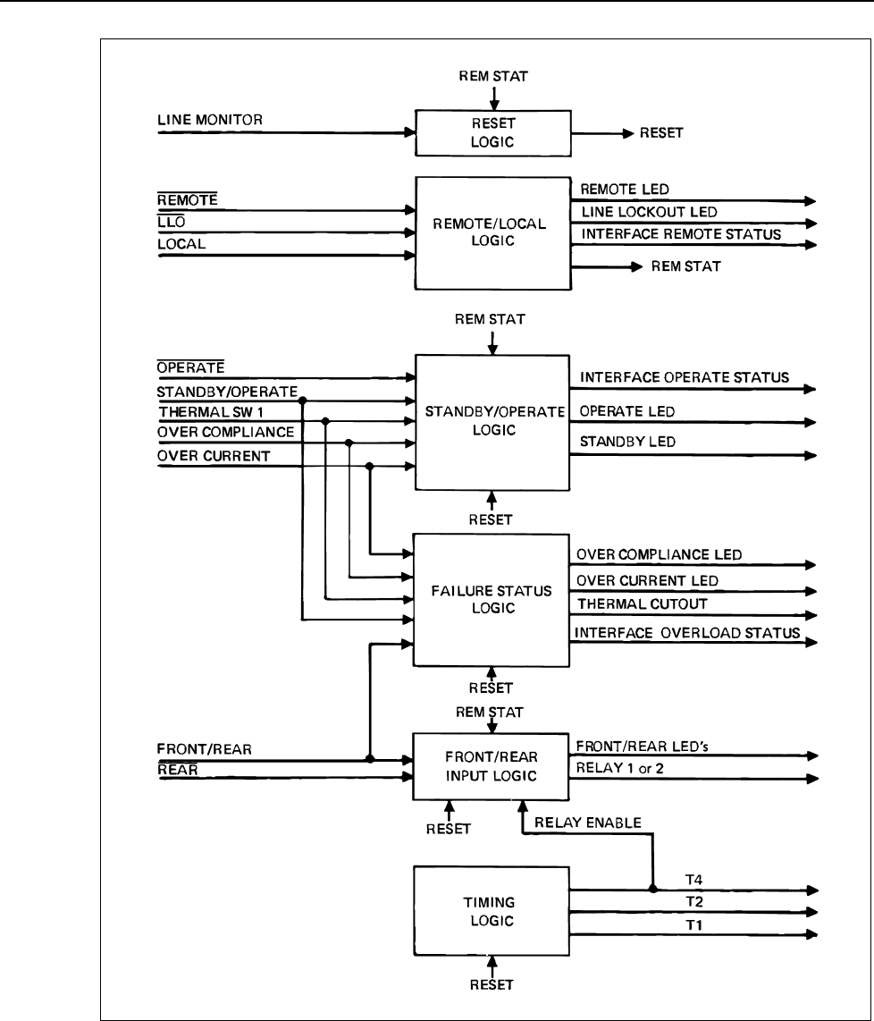
5220A
Instruction Manual
3-12
ajs13f.wmf
Figure 3-8. A10 Logic Simplified Block Diagram
Loss or interruption of the +15/-15 V dc supply output causes the Line Mon (monitor)
input from the power supply to go low. Normally, the line monitor input is a clipped full-
wave rectified 60 Hz waveform which is generated on the A4 Regulator Assembly. The
negative-going edge is used as the trigger for monostable U11-7 which is timed to
provide an output pulse of approximately 0.1 second. Since the output is longer than the
time between triggers, it will remain active (Q low) as long as the Line Mon (monitor)
Theory of Operation
Circuit Analysis
3
3-13
input is present. Under normal operating condition the reset command is high at U9-10
and low at U3-10.
When the 5220A is switched from remote to local operation the local/remote logic
triggers monostable U11-10 in the reset logic circuit. The result is a momentary positive-
going pulse at the Q output of U11-10. This in turn drives the complementary reset lines
of U9-10 and U3-10.
The overall result of a reset command, regardless of how it is initiated, is to set the output
commands of the A10 Logic to the states shown in Table 3-1. Essentially the unit is
commanded to standby operation with front panel inputs selected. Remote and Local
Lockout (LLO) commands are not affected by the reset command.
Table 3-1. Effect of Reset Command on A10 Logic and A9 Front Panel
Signal Name Logic State Front Panel LED Status
Interface Operate Status Low None
Operate LED High OPER LED off
Standby LED Low STDBY LED on
T1, T2, and T4 Low None
Relay 1 High None
Relay 2 High None
Front Panel Input LED Low FRONT LED on
Rear Panel Input LED High FRONT LED OFF
Overcompliance LED High OVERCOMPLIANCE LED off
Overcurrent LED High OVERCURRENT LED off
Thermal Cutout LED High THERMAL CUTOFF LED off
Interface Overload Status Low None
3-15. Timing Logic
The timing logic controls the timing sequence used to switch the transconductance
amplifier between the standby and operate modes. It consists of a bi-directional shift
register U22, D-type flip-flops U17-1, and free running multivibrator U23. The
multivibrator runs at a frequency of 100 Hz (10 ms period) and serves as the clock for
both the flip-flop and the shift register. Flip-flop U17-1 responds to the Reset command
(reset input) and the standby/operate commands (D-input) to select the shift register’s
control mode; i.e., shift left or shift right. The shift register’s four outputs are sequenced
low in the shift-left mode and high in the shift-right mode. With all outputs low the
transconductance amplifier is set to standby. The amplifier is operational when all output
are high.
The shift-left mode is selected when flip-flop U17-1 drives the register’s S0 input low and
its S1 input high. (This occurs as the result of a standby or reset command.) In this mode
the register sequentially propagates the low input at U22-7 through the register causing
its four outputs (QA, QB, QC, and QD) to be sequentially driven low. Since the register
shifts at the rate of the 100 Hz clock, the outputs are sequenced at intervals of 10 ms. At
the end of four clock pulses all four outputs are low (standby), and will remain low until
the register is commanded to shift right.
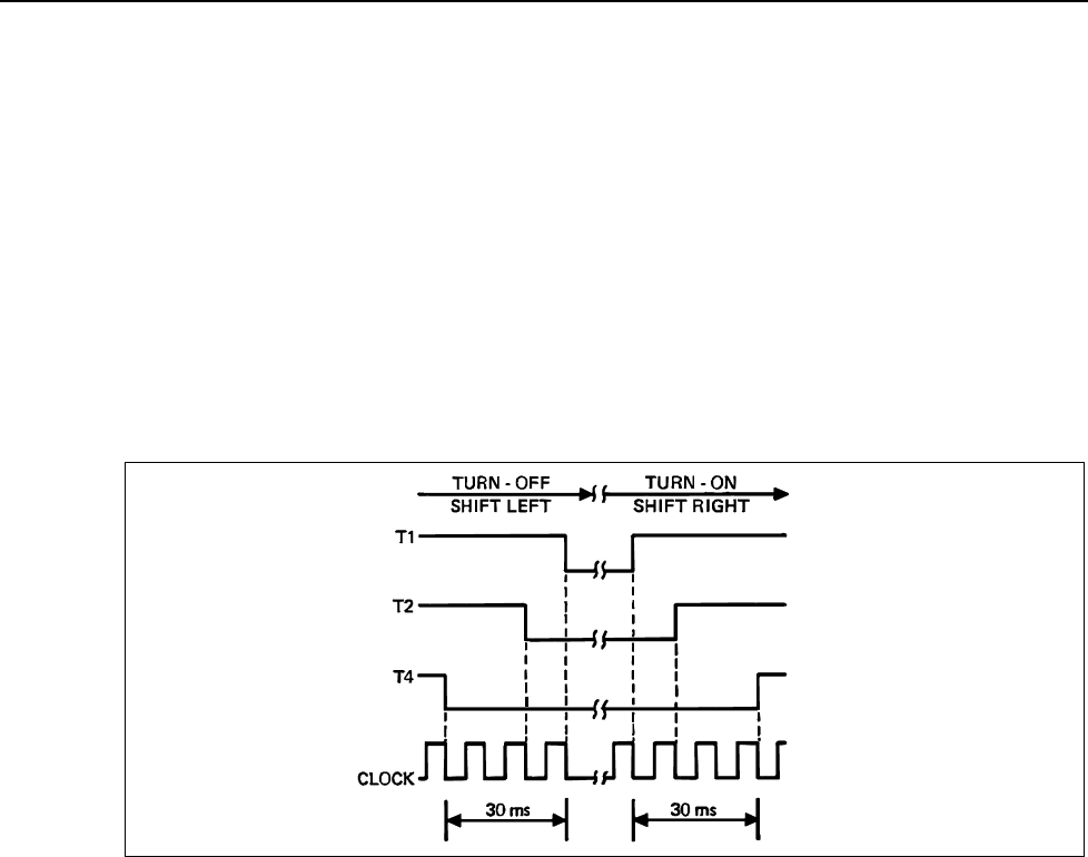
5220A
Instruction Manual
3-14
The shift-right mode is selected when flop-flop U17-1 responds to an operate command
(D-input low) and drives the register’s S0 input high and the S1 input low. This results in
the high input at U22-2 being sequentially propagated through the register and its four
outputs (QD, QC, QB and QA) being driven high (operate).
The outputs of the shift register are used as control signals to sequence the turn-on and
turn-off of the transconductance amplifier. They are designated T1, T2, and T4 (T3 is not
used) and their sequence is shown in Figure 3-9. The control function of each of the
signals is as follows:
1. T1 turns the A6 Driver on and off.
2. T2 turns the A5 Preamplifier on and off.
3. T4 enables/disables the selected front/rear input relay (K1 or K2) on the A5
preamplifier.
ajs14f.wmf
Figure 3-9. Timing Sequence
3-16. Standby/Operate Logic
The standby/operate logic consists of optical isolators U1 and U5, monostable U8-7, D-
type flip-flop U10-9, and a series of supporting logic gates and buffers. Its function is
twofold. One, it responds to reset and external inputs to command the state of the timing
logic, shift left (standby mode) or shift right (operate). Two, it drives the front-panel
STANDBY/OPERATE LEDs and provides the A11 MIS Bus Interface (remote interface)
with an Interface Operate Status (Standby/Operate) signal. Flip-flop U10-9 is used to
store the commanded mode (standby or operate) and to provide the necessary commands
to the shift register (in the timing logic) and the LED/status drivers. Optical isolators U1
and U5 are used to electrically isolate remote control signals to and from the A11 MIS
Bus Interface from the A10 Logic.
Standby/operate commands occur in the form of Reset, Standby/Operate, not Operate,
Sw(itch) 1, Overcompliance, and Overcurrent. Reset is an onboard command from the
reset logic. It sets the 5220A to standby by commanding U10-9 to the clear state (Q low).
Standby/Operate is received in the form of a +5 V (high) input each time the front-panel
STANDBY/OPERATE switch is pressed. If the 5220A is in the local control mode, each
press of the switch will clock flip-flop U10-9 to its alternate state. The result is an
alternate selection of either the standby or the operate mode, as indicated by the front-
panel STANDBY and OPERATE LEDs. A similar command, Interface Operate Status
(also derived from the state of U10-9), is issued to the A11 MIS Bus Interface; low

Theory of Operation
Circuit Analysis
3
3-15
indicates standby, high indicates operate. The not Operate signal is received from the
A11 MIS Bus Interface and is effective only when the 5220A is in the remote control
mode. In the high state, the signal clears flip-flop U10-9 to invoke the standby mode.
When not Operate goes low it presets flip-flop U10-9 (by way of U8-7) to invoke the
operate mode. Overload signals received at the standby/operate logic include; Thermal
Sw(itch) 1, Overcompliance and Overcurrent. When any one of these signals goes high,
flip-flop u10-9 is cleared to the standby state.
3-17. Local/Remote Logic
The local/remote logic consists of optical isolators U4 and U20-8, monostable U8-9,
D-type flip-flop U7, and a series of supporting logic gates and buffers. Its function is to
enable selection of the desired control mode (local or remote) and to provide the drive for
the appropriate front panel and A11 MIS Bus Interface status indicators. These include
LLO (Local Lock Out) LED, Remote LED, and Interface Remote Status. Flip-flop U7 is
used to store the commanded mode (local or remote) and to provide the necessary
commands to the onboard logic and the LED/status drivers. Optical isolators U4 and
U20-8 electrically isolate remote control signals to and from the A11 MIS Bus Interface
from the A10 Logic.
Local/remote commands are received in the form of Local, not Remote, and not LLO
(Local Lockout). Local occurs as a momentary +5 V (high) input each time the front
panel LOCAL switch is pressed. If the 5220A is in the remote control mode and Local
Lockout is not commanded (high) pressing the front panel LOCAL switch will initiate a 1
µs pulse from monostable U8-9. This pulse clears flip-flop U7, which in turn, commands
the A10 Logic to the local mode (Rem Stat low). As a result, the Remote LED and LLO
LED signals are high, Interface Remote Status is low. However, if not LLO is low when
the LOCAL switch is pressed, monostable U8-9 will be held in the reset state and flip-
flop U7 will not be cleared. Thus, the A10 Logic is effectively locked into the remote
mode until not LLO is returned high.
The not Remote signal is received from the A11 MIS Bus Interface and is used to
remotely command the A10 Logic to the remote control mode. When the signal goes low
it is coupled across optical isolator U4 to the clock input of D-type flip-flop U7. This sets
the Q Output of U7 high to select the remote control mode (Rem Stat high). As a result,
the Remote LED signal goes low to light the REMOTE LED and the Interface Remote
Status output goes high.
When the 5220A is commanded to the remote mode the front-panel
STANDBY/OPERATE and FRONT/REAR switches are disabled and the corresponding
remote inputs are enabled. Similarly, if LLO is remotely enabled, the LOCAL pushbutton
is disable.
3-18. Front/Rear Input Logic
The front/rear input logic is used to command the front/rear input relays on the A5
Preamplifier and to drive the appropriate FRONT/REAR LED on the front panel. When
the A10 Logic is in the local mode, Front/Rear commands are received from the front
panel pushbutton. Each switch depression is received as a +5 V (high) level that is used
to clock alternate states on D-type flip-flop U10-5. The FRONT LED and Relay K1 are
commanded when the Q output of U10-5 is low. When the A10 Logic is in the remote
mode the not Rear input signal is used to command the front/rear input relays. Front input
is selected when not Rear is high. Actual opening/closing of the relays is enabled at time
T4 of the timing logic.

5220A
Instruction Manual
3-16
3-19. Failure Status Logic
The failure status logic consists of three D-type flip-flop (U16-1, U16-13, and U17-13)
and their associated logic gates and drivers. Its function is to store failure conditions
detected by other parts of the A10 Logic and to drive the front panel STATUS indicators.
An optical isolator is also included for providing an Interface Overload Status signal to
the A11 MIS Bus Interface. Front panel status indicators comprise three LEDs:
OVERCOMPLIANCE, OVERCURRENT, and THERMAL CUTOUT. When any one of
these LEDs is lit, Interface Overload Status is driven high.
The inputs to the D-type flip-flop are connected to respond to three commands: reset,
clock, and set. The reset and clock inputs are used to set the Q outputs low, and thereby
remove the drive from the front panel STATUS LEDs. The three reset inputs are
connected in parallel and are commanded when the 5220A is initially energized and
when it is remotely commanded from standby to operate. The clock inputs are also
connected in parallel. They respond to a high input that transfers the low D-input to the Q
output. The clock is driven high under the following conditions:
1. When the STDBY/OPR pushbutton is pressed.
2. When the FRONT/REAR pushbutton is pressed.
3. When an onboard reset is initiated.
The set-inputs to the flip-flops in the failure status logic are used to set the Q outputs high
when a failure status is detected. This causes the corresponding STATUS LED to be lit
and the Interface Overload Status signal to go high. Each flip-flop responds to one of the
failure signals issued by the transconductance amplifier. They are:
1. Thermal Sw(itch) 1
2. Overcompliance
3. Overcurrent
3-20. A11 MIS Bus Interface
The A11 MIS Bus Interface, as shown in Figure 3-10, is a remote control interface that
allows the 5220A to operate as an extension of a 5100 Series Calibrator equipped with a
Model Y5000 Interface. An accessory cable is available for use with the Y5000 to
complete the necessary connections between the Y5000 and the A11 MIS Bus Interface.
Functionally, the A11 MIS Bus Interface (hereafter referred to as the MIS I/F) performs
three basic functions: receives and stores digital control data from a remote control
source (Y5000), interfaces 5220A status signals to the Y5000, and provides a connecting
path between the remote analog input signal (Aux Out) and the rear-input connections on
the A5 Preamplifier. Operating power for the assembly is derived from the +5 V ISO
(isolated) power supply.
Control data is received at the MIS I/F via the data bus as a 4-bit parallel word. When the
5100 Series Calibrator places the correct address on the address bus (BC0, BC3, and BC6
high), the write data logic responds by pulling the not ACK (acknowledge) line low and
clocking the control data word into the data register, U1. The not ACK signal is sent to
the 5100 to acknowledge the receipt of a valid address. The register outputs are buffered
and inverted by U6 before being used as remote programming inputs to the A10 Logic
PCB (i.e., not Remote, not Operate, not LLO and not Rear). At the same time that the
address is acknowledged, an RS flip-flop in the write data logic is set.
The function of the RS flip-flop is to prevent two successive status read inputs to the
5220A. The flip-flop is set when a high is present on inputs BC0, BC3, and BC6. This
results in a low output from U5-8 and a high output from U4-6. In this state gate U5-8 is
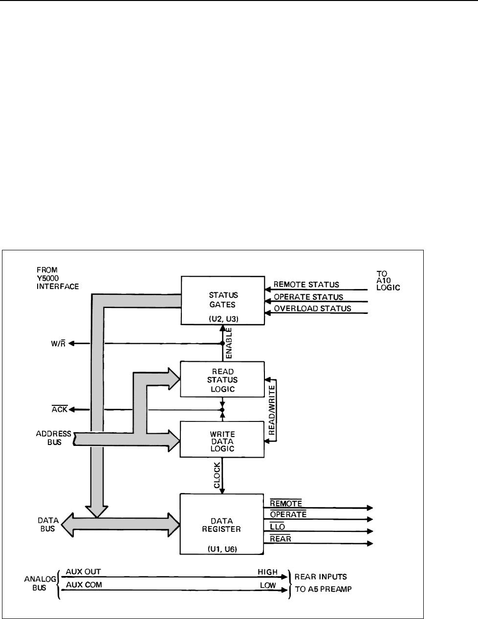
Theory of Operation
Circuit Analysis
3
3-17
enabled so that a status read can take place when BC0 and BC2 go high. Status read
causes the w/not R line to go low for the duration of the BC0 and BC2 inputs. At the end
of status read, the RS flop-flop is reset, closing the w/not R gate (U5-8) until it is
reopened by another programming input. This process is repeated every 16 ms because
the 5100 Series Calibrator refreshes the programming input to the 5220A at this rate.
Status information is received at the MIS I/F as three bits of parallel data (Remote Status,
Operate Status, and Overload Status) from the A10 Logic. When the 5100 Series
Calibrator places the correct address on the address bus (BC0 and BC2 high), the read
status logic responds by pulling the not ACK line low and gating the three status bits onto
the data bus. The not ACK signal is sent to the 5100 to acknowledge the receipt of a valid
address. At the same time the RS flip-flop in the read status logic is reset. This causes a
read command (W/nor R low) to be sent to the 5100 so that it can read the data bus. The
acknowledge output and the w/not R line will return high when the status address code is
removed from the address bus.
The analog output from the 5100 is passed through the Y5000 and the MIS I/F by way of
a two-wire (high, low) analog bus. The signal is routed directly from the MIS I/F to the
rear input connections on the A5 Preamplifier.
BDO-BD2
BCO, BC2
BCO, BC3, BC6
BDO-BC3
ajs06f.wmf
Figure 3-10. A11 MIS Bus Interface

5220A
Instruction Manual
3-18

4-1
Section 4
Maintenance
4-1. Introduction
WWarning
These servicing instructions are for use by qualified personnel
only. To avoid electric shock, do not perform any servicing
other than that contained in the operation instructions unless
you are qualified to do so.
This section of the manual contains maintenance information for the Model 5220A
Transconductance Amplifier. The material is presented under the categories of shipping
information, general maintenance, performance test, calibration adjustments, and
troubleshooting. The performance test is recommended as an acceptance test when the
unit is first received, and later as a calibration procedure to verify the 180-day
specifications. Table 4-1 lists the equipment required for both the performance test and
calibration adjustments. If a recommended model is not available, an equivalent
instrument meeting the required characteristics can be substituted.
Table 4-1. Required Test Equipment
Equipment Type Required Specifications Recommended Type
DC and AC Voltage Calibrator 0 to 20 V dc ±0.002 % Fluke Model 5700A
Digital Multimeter 0 to 20 V dc ±0.002 %, Resolution: 1 µV HP3458A
Precision Shunt 0.01 Ω ±0.01 % dc, 0.035 % ac to 5 kHz Fluke Model Y5020
Load Resistor 0.01 Ω ±3 %, 50 W Dale RH-50
Load Resistor 0.01 Ω ±5 %, 10 W Dale RH-10
Distortion Analyzer Frequency range: 100 Hz to 5 kHz Sound Technology Model
1700A
Autotransformer Nominal line voltage ±10 %, 500 W General Radio Variac

5220A
Instruction Manual
4-2
4-2. Service Information
The 5220A is warranted for a period of 1-year upon delivery to the original purchaser.
The warranty is located on the back of the title page.
Factory authorized calibration and service for each Fluke product is available at various
worldwide locations. A complete list of these service centers is included in Section 7 of
this manual. If requested, an estimate will be provided to the customer before work is
begun on instruments that are beyond the warranty period.
4-3. General Maintenance
4-4. Cleaning
Clean the 5220A periodically to remove dust, grease, and other contamination. Use the
following procedure:
1. Clean the front panel and case with a soft cloth dampened with a mild solution of
detergent and water.
2. Clean the surface of the PCBs using clean, dry air at low pressure (<20 psi). If grease
is encountered, spray with Freon T.F. Degreaser and remove grime with dry, low-
pressure air.
4-5. Air Filter Maintenance
Periodically inspect the air filter on the rear panel for dirt and contaminants. If cleaning is
required, use the following procedure:
1. Disconnect the 5220A from line power.
2. Remove the two screws from the filter housing and gently pull the filter assembly
from the unit.
3. Clean the filter using either low-pressure air or a mild solution of detergent and
water.
4. Dry (if necessary) and reinstall the filter.
4-6. Access Information
The 5220A is a modular instrument that can be easily disassembled by sections.
Procedures for section disassembly are given in the following paragraphs. Some
procedures require the completion of previous procedures in the disassembly process.
When this occurs, the previous procedure will be referenced, but not repeated.
WWarning
To avoid electrical shock hazard, disconnect he 5220A from line
power before attempting any of the following disassembly
procedures.
Reassembly of the instrument is accomplished by logically reversing the disassembly
procedure. Before installing the top covers on the unit, make a visual comparison with
Figure 4-1 to ensure the presence of all assemblies, jumpers, and fuses.
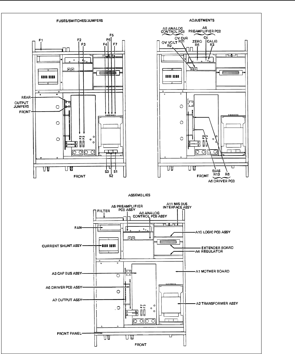
Maintenance
General Maintenance
4
4-3
ajs15f.wmf
Figure 4-1. Internal Component/Assembly Locations
Caution
To prevent component damage observe static awareness
precautions during instrument disassembly/assembly. Refer to
the yellow insert sheet following Section 1.

5220A
Instruction Manual
4-4
4-7. Internal Components/Assemblies
All internal switches, fuses, and calibration adjustments can be accessed by removing the
top cover and the large inner cover from the 5220A. The location of each of the
applicable components is shown in Figure 4-1. Procedures for setting, replacing, and/or
adjusting these components are given later in this section of the manual.
4-8. Front Panel Removal
There are no electrical components physically mounted on the front panel of the 5220A.
Use the following procedure to remove the front panel:
1. Remove the top and bottom covers from the 5220A.
2. Stand the instrument on its rear handles. Use a solid work surface.
3. Locate the two tabs at the rear of each front handle and remove the tab screws (4
total).
4. Lift the front panel from the chassis.
4-9. A9 Front Panel PCB Removal
Use the following procedure to access and remove the A9 Front Panel PCB Assembly:
1. Remove the front panel.
2. Remove the two screws from the top of the A9 Front Panel PCB Assembly.
3. Pull the PCB from its connector (J10).
4-10. A2 Transformer Assembly Removal
Use the following procedure to remove the A2 Transformer Assembly from the 5220A:
1. Remove the top cover from the 5220A.
2. Remove the large inner cover.
3. Locate and remove the two screws that hold the A2 Transformer Assembly to the
chassis side.
4. Remove the two screws that hold the A2 Transformer Assembly to the Motherboard.
These screws are located on the bottom right-side of the transformer assembly (as
viewed from the top rear of the 5220A).
5. Remove the two hex screws that hold the top front of the transformer assembly to the
5220A front bulkhead.
6. Disconnect the three high-current transformer leads at the A3 Cap Bus Assembly.
Lug nuts hold the leads in place.
Note
When reassembling, the clear colored lead (center top) must be connected
to the terminal marked T. Connect one black lead to terminal S and the
other to terminal F.
7. Carefully lift the A2 Transformer Assembly from the 5220A.

Maintenance
General Maintenance
4
4-5
4-11. A6 Driver and A7 Output Assembly Removal
The A6 Driver and A7 Output PCB Assemblies comprise a plug-in assembly referred to
in this procedure as the A6 Driver/A7 Output. Use the following procedure to remove the
A6 Driver/A7 Output:
1. Remove the top cover from the 5220A.
2. Remove the large inner cover.
3. Remove the four screws from the sheet-metal portion of the A7 Output Assembly.
4. Remove the lug nuts holding the +12 and –12 V bus straps to the A3 Cap Bus.
5. Remove the front/rear output selection screws (jumpers).
6. Lift the A6 Driver/A7 Output from the chassis.
4-12. A3 Cap Bus Removal
To remove the A3 Cap Bus from the 5220A use the following procedure:
1. Remove the top and bottom covers from the 5220A.
2. Remove the top inner cover.
3. Remove both the front panel and the A9 Front Panel PCB Assembly.
4. Remove the A6 Driver/A7 Output Assembly.
5. Disconnect the transformer leads at the A3 Cap Bus.
6. Remove the two screws that secure the A3 Cap Bus ground strap to the motherboard.
7. Remove the nine screws holding the A3 Cap Bus to the front panel bulkhead.
8. On the A3 Cap Bus locate and the remove the two large-head screws located to the
side of resistors R2 and R5.
Caution
When these screws are installed they should be snug with the
PCB. However, they should not cause the PCB to bow.
9. Lift the A3 Cap Bus from the chassis.
Note
A heat-sink compound has been applied to the diode-end of the A3 Cap Bus.
Do not wipe off or otherwise remove this compound.
4-13. A12 Shunt Assembly Removal
Use the following procedure to remove the A12 Shunt Assembly:
1. Remove the top cover from the 5220A.
2. Remove both the large and small inner covers.
3. Remove the A8 Analog Control PCB Assembly from its connectors (J40).
4. Unplug the red-/black-lead connector next to J50 on the motherboard.
5. Locate the A12 Shunt Assembly (just in front of the fan) and remove the two screws
at the base of the assembly).
6. Carefully pull the A12 Shunt Assembly straight up while feeding the red-/black-leads
under the bulkhead. When the leads are free, remove the A12 Shunt Assembly from
the chassis.
Note
When reinstalling the shunt make sure that the red-/black-leads are plugged
into the motherboard; red lead to pin R, black lead to pin B.

5220A
Instruction Manual
4-6
4-14. Fuse Replacement
4-15. Ac Line Fuse
The ac line fuse is accessible by way of a rear-panel fuse holder located to the left of the
input power connector. If fuse replacement is required, disconnect the 5220A from line
power and remove the fuse cap and fuse (twist the fuse cap ccw using a screwdriver).
Select and install a replacement fuse whose rating is compatible with the local line
voltage.
• 100 to 120 V ac: Use fuse type MDA 3 A
• 220 to 240 V ac: Use fuse type MDX 1.5 A
4-16. Power Supply Fuses
There are six fuses located inside of the 5220A. Each is used to fuse one of the secondary
windings of the power transformer. Four of the fuses are located on the A2 Transformer
Assembly, and two are on the A3 Cap Bus. Their locations (F2 through F7) are shown in
Figure 4-1. Use the following procedure when replacement is necessary:
1. Disconnect the 5220A from line power.
2. Remove the top and large inner covers from the 5220A.
3. With reference to Figure 4-1, locate and inspect fuses F2 through F7. The fuses are
installed in fuse clips and can be pulled out using your fingers.
4. Replace defective fuses with the appropriate type and rating:
a. F2 and F3 are AGC 20 A fuses.
b. F4 through F7 are MDL 1/2 A fuses.
4-17. Line Voltage Selection
The 5220A is set at the factory to operate at a line voltage of either 115 or 230 V ac
+10%, 40 to 60 Hz. The selected voltage is identified on a rear panel decal. If your local
line voltage is not within this preset range, a suitable range may be selected by setting a
series of three switches (S1, S2, S3) on the A1 Transformer Assembly. Figure 4-2 shows
the switch locations as well as the switch settings for eight different line voltages. Use the
following procedure to set the line voltage switches:
1. Disconnect the 5220A from line power.
2. Remove both the top cover and the large inner cover from the 5220A.
3. With reference to Figure 4-2, locate and set switches S1, S2, and S3 to the positions
indicated for the desired line voltage.
4. Reinstall the top and inner covers.
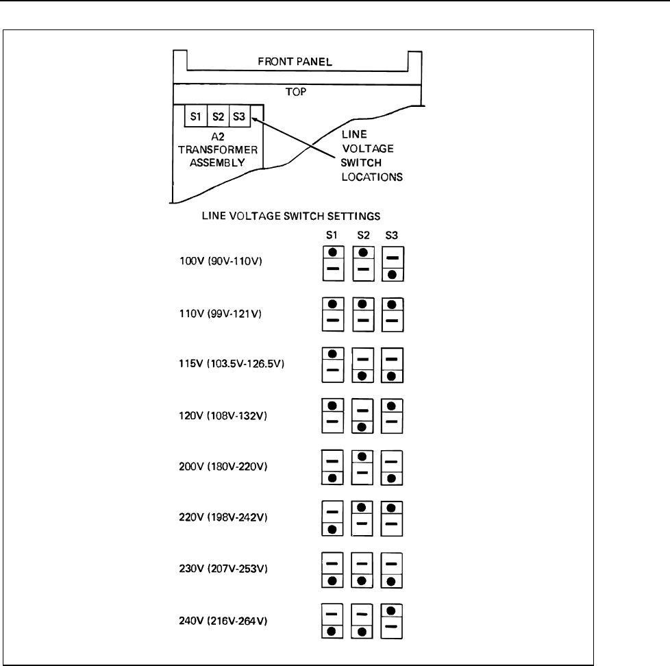
Maintenance
General Maintenance
4
4-7
ajs16f.wmf
Figure 4-2. Line Voltage Selection
4-18. Output Terminal Selection, Front/Rear
Either the front or rear output terminals (but not both simultaneously) may be selected to
provide the current output connections. The active terminals are determined by the
position of a pair of screws that serve as output jumpers. See Figure 4-1 for the output
jumper (screw) locations. Installing the screws in the two holes marked FRONT enables
the front CURRENT OUTPUT terminals. Similarly, installing the screws in the two holes
marked REAR enables the rear output terminals. Use the following procedure to position
the screws:

5220A
Instruction Manual
4-8
Caution
To ensure proper instrument operation make sure that both
screws are installed and that they are both in either the FRONT
or REAR locations.
1. Disconnect the 5220A from line power.
2. Remove both the top and large inner covers from the 5220A.
3. Locate the output jumper screws as shown in Figure 4-1.
4. Install and secure the screws in the two FRONT or REAR holes, as desired.
5. Reinstall the top and inner covers.
4-19. Service Tools
The 5220A comes equipped with an extender board for servicing other 5220A PCB
assemblies. A storage slot for the board is provided in the 5220A PCB assemblies. See
Figure 4-1 for the storage location.
4-20. Performance Test
The following paragraphs comprise a performance verification test that compares the
instrument’s performance to the specifications given in Section 1 of this manual. The test
is recommended as an acceptance test when the unit is first received, and later as a
calibration procedure to verify instrument accuracy at the scheduled calibration periods.
It is also useful as an aid in troubleshooting.
Test equipment required for the performance test is listed earlier in Table 4-1. If the
recommended equipment is not available, comparable instruments with equivalent
specifications may be substituted. To ensure optimum results, the test must be performed
at an ambient temperature of 22 to 24 degrees Celsius, with a relative humidity of less
than 85 %. Also the instrument should be allowed to warm up for at least 30 minutes
before starting the performance test.
If the instrument does not meet the performance test, troubleshooting, repair, and/or
calibration adjustment is indicated. Procedures for calibration adjustment and
troubleshooting are given later in this section of the manual.
4-21. Initial Conditions
Before starting the following procedures, condition the 5220A as follows:
1. Disconnect all input, output, and remote connections at the 5220A.
2. Install the top, bottom and inner covers if they have been removed.
3. Connect the unit to line power through an autotransformer set for the proper line
voltage, and set the POWER switch to ON. Only the STANDBY and FRONT LEDs
should light.
4. Allow the 5220A to warm up for at least 30 minutes before proceeding.

Maintenance
Performance Test
4
4-9
4-22. Front Panel Tests
Use the following procedure to check the operation of the 5220A front-panel controls and
LEDs:
1. With the unit in the standby mode, connect jumper wires between the enabled
(front/rear) output terminals. Use a 4-inch length of 16-gauge insulated wire.
2. Press the OPR/STDBY pushbutton. The OPR LED should light and the STDBY LED
should go out.
3. Press the INPUT pushbutton to select the rear input.
4. Return input control to the front panel by pressing the INPUT pushbutton. The
FRONT LED should light and the REAR LED should go out.
5. Remove the jumper wire from the output terminals. The unit should switch to the
standby mode and the OVERCOMPLIANCE LED should light.
6. Reinstall the jumper wire at the output terminals.
7. Clear the overcompliance condition by pressing the OPR/STDBY switch. Set the unit
to the operate mode.
Caution
The THERMAL CUTOFF LED will light only when the output
stage of the 5220A is overheated. This is a failure mode that
should not be invoked for test purposes. The LOCAL
pushbutton and the REMOTE, LOCAL LOCK OUT LEDs are
remote control features that require remote commands for
operation.
4-23. Zero Output
The following procedure checks the zero output of the 5220A in both the standby and
operate modes:
1. Connect the load resistor (0.1 ohm) to the enabled (front/rear) output terminals.
2. Connect the DVM to the sense terminals on the load resistor and select the 100 mV
dc range.
3. With the 5220A in the standby mode, read the voltage drop across the load resistor.
The reading should be 0 +/-5 µV dc.
4. Connect a short jumper wire between the front VOLTAGE INPUT terminals.
5. Set the 5220A to the operate mode. The OPERATE LED should be on and the
STANDBY LED off.
6. Read the output voltage on the DVM. It should be 0 +/-100 µV dc.
7. Set the 5220A to standby and remove the jumper wire from the VOLTAGE INPUT
terminals.
8. Disconnect the load resistor from the output terminals on the 5220A.
5220A
Instruction Manual
4-10
4-24. DC Accuracy and Line Regulation
The following procedure is used to check the dc accuracy of the 5220A output current:
1. Connect the precision shunt to the enabled output terminals on the 5220A.
2. Connect the DVM to the sense terminals on the precision shunt. Observe polarity.
3. Set the DVM to the 200 mV dc range.
4. Connect the output of the dc voltage calibrator to the VOLTAGE INPUT terminals
on the 5220A; positive to red, negative to black.
5. Set the dc voltage calibrator to the output shown in step 1 of Table 4-2 (+10.0000 V
dc).
6. Set the 5220A to the operate mode.
7. Using the DVM reading and the calibrated shunt valve, calculate the output current
(I = E/R). The calculated value should be within the limits shown in the table.
8. Vary the line voltage +10 % from nominal and verify a less than 0.001 % change in
output current.
9. Sequentially set the calibrator output to the voltages shown in steps 2 and 3 of Table
4-2. At each voltage setting verify the 5220A output accuracy by repeating step 7 of
this procedure.
10. Set the 5220A to the standby mode.
11. Set the dc voltage calibrator output to zero volts and disconnect it from the 5220A.
12. Disconnect the precision shunt from the 5220A output terminals.
Table 4-2. DC Accuracy Test
Step DC Calibrator Output (V dc) Calculated Output Current (Amps)
1 +10.0000 +9.9965 to +10.0035
2 +20.0000 +19.9940 to +20.0060
3 -10.0000 -10.0035 to –0.0065
4-25. Harmonic Distortion
This procedure is used to measure the harmonic distortion present at the output of the
5220A.
1. Set the output of the ac voltage calibrator to zero and connect it to the 5220A
VOLTAGE INPUT terminals.
2. Connect the load resistor (0.1 ohms) to the enabled (front/rear) output terminals.
3. Connect the distortion analyzer to load resistor sense terminals.
4. Set the ac voltage calibrator output to 20 V rms at 1 kHz.
5. Set the 5220A to the operate mode.
6. Measure the output distortion on the distortion analyzer. It should be less than or
equal to 0.075 %.
Note
Do not use input filters when making this measurement.
Maintenance
Performance Test
4
4-11
7. Set the 5220A to the standby mode.
8. Disconnect the load resistor and the distortion analyzer from the 5220A output
terminals.
4-26. Frequency Response
Note
When high ac currents at high frequencies are being used, and
minimization of inductive coupling is required, it is recommended that you
twist the current carrying leads between the 5220A and load. Also, any
measuring instruments used with the load should be kept at least eighteen
inches away the load to prevent radiation from affecting its reading.
The frequency response of the 5220A is checked using the following procedure:
1. Connect the precision shunt (.01 ohm) to the enabled (front/rear) output terminals.
2. Connect the true rms voltmeter to the sense terminals on the precision shunt.
3. Set the ac voltage calibrator output to the voltage and frequency shown in step 1 of
Table 4-3 (20.0000 V @ 100 Hz).
4. Set the 5220A to the operate mode.
5. Read the true rms voltmeter and calculate the current. It should indicate a current
within the limits shown for step 1.
6. Sequentially set the calibrator output to each of the frequencies shown in steps 2
through 5 of Table 4-3. At each frequency verify that the measured current is within
the limits given for that step.
7. Set the 5220A to the standby mode.
8. Disconnect the precision shunt from the 5220A output terminals.
Table 4-3. Frequency Response Test
Step AC Voltage Calibrator Output (V rms) Measured Output Current (Amps)
1 20 V @ 100 Hz 19.970 to 20.030*
2 20 V @ 300 Hz Reading 1 ±0.05 %
3 20 V @ 1 kHz Reading 1 ±0.05 %
4 20 V @ 3 kHz Reading 1 ±0.15 %
5 20 V @ 5 kHz Reading 1 ±0.25 %
* Includes limit of errors:
1. 5220A 2. 5200A 3. Y5020 4. 931A
4-27. Overcurrent Trip Test
The following procedure will verify the accuracy of the overcurrent trip setting on the
5220A:
1. Connect the load resistor (0.1 ohm) to the enabled (front/rear) output terminals.
2. Set the output of the ac voltage calibrator to 20.0000 V rms.
3. Set the 5220A to the operate mode.

5220A
Instruction Manual
4-12
4. Increase the ac voltage calibrator output in 1.0V rms increments. The 5220A should
switch to the standby mode at between 20.0 and 24.0 V rms. The OVERCURRENT
LED should also light.
5. Set the ac voltage calibrator output to zero volts.
6. Disconnect the load resistor from the 5220A output terminals.
4-28. Overvoltage Trip Test
The following procedure is used to check the overvoltage trip setting on the 5220A:
1. Connect a 1 ohm ±5 %, 10 W resistor (Dale RH-10) to the enabled (front/rear) output
terminals on the 5220A.
2. Set the output of the 5220A to 3.0000 V rms.
3. Set the 5220A to the operate mode.
4. Increase the ac voltage calibrator output in 0.1 V rms increments. The 5220A should
switch to the standby mode with an input of 3.1 to 3.5 V rms. The OVERVOLTAGE
LED should also light.
5. Set the ac voltage calibrator output to zero volts and disconnect the unit from the
5220A.
6. Remove the 1 ohm, 10 W resistor from the 5220A output terminals.
7. Set the 5220A POWER switch to OFF.
4-29. Calibration Adjustments
The calibration adjustment procedures given in the following paragraphs should be
performed after repair of the 5220A and/or when the unit fails the performance-test
requirements. If the unit will not respond to, or meet the limits of the adjustment
procedures, troubleshooting and repair is indicated. Equipment required for the
calibration adjustments is listed earlier in Table 4-1.
All calibration adjustments are accessible when the top and large inner covers are
removed from the 5220A. Figure 4-1 identifies the location of the assemblies, test points,
and adjustments that must be accessed to complete the calibration adjustment procedures.
To ensure optimum results, the calibration adjustments must be performed at an ambient
temperature of 22 to 24 degrees Celsius, with a relative humidity of less than 85 %. Also
the unit should be allowed to warmup in the operate mode (with the top cover in place)
for at least 30 minutes before starting the adjustment procedures.

Maintenance
Calibration Adjustments
4
4-13
4-30. Initial Conditions
Before starting the following procedures, condition the 5220A as follows:
1. Disconnect all input and remote connections to the 5220A, and connect a short
jumper wire between the selected output terminals.
2. Connect the unit to line power and set the POWER switch to ON. Only the STDBY
and FRONT LEDs should light.
3. Set the 5220A to the operate mode and allow it to warmup for at least 30 minutes.
4. Remove the top and large inner cover from the unit, and complete the following
procedures.
4-31. Input Offset Adjustment
The following procedure is used to adjust input offset (R6) on the A5 Preamplifier PCB
Assembly:
1. Connect the load resistor (0.1 ohm) to the enabled (front/rear) 5220A output
terminals.
2. Connect the DVM to the sense terminals on the load resistor and select the 100 mV
dc range.
3. Connect a short jumper wire between the front VOLTAGE INPUT terminals.
4. Set the 5220A to the operate mode.
5. Adjust R6 on the A5 Preamplifier PCB Assembly for a DVM reading of -.010 to -
.010 mV dc (0 +10 µV dc).
6. Set the 5220A to the standby mode.
4-32. Driver Offset Adjustment
The following procedure is used to adjust input offset (R6) on the A6 Driver PCB
Assembly. The procedure is accomplished with the 5220A in the standby mode:
1. Jumper test lead between TP7 (-15 V dc) on the A4 Regulator and TP4 (Turn on 1)
on the A8 Analog Control. This enables the A8 Analog Control and A7 Output while
the A5 Preamplifier is clamped to zero (standby).
2. Adjust R6 on the A6 Driver for a DVM reading of -1.000 to +1.000 mV dc.
3. Disconnect the test lead from TP4 and TP7.
4. Remove the load resistor from the 5220A output terminals.
5. Remove the jumper wire from the front-panel VOLTAGE INPUT terminals.

5220A
Instruction Manual
4-14
4-33. Output Bias Adjustment
This procedure is used to adjust the bias current for both the A6 Driver and the A7
Output. The bias adjustment (R13) is located on the A6 Driver PCB Assembly.
1. Connect the ac voltage calibrator to the front-panel VOLTAGE INPUT terminals on
the 5220A.
2. Connect the load resistor (.1 ohm) to the enabled output terminals on the 5220A.
3. Connect the distortion analyzer input to the sense terminals on the load resistor.
4. Set the ac voltage calibrator for a 20 V rms, 1 kHz output.
5. Set the 5220A to the operate mode.
6. Measure the distortion and adjust R13 for a minimum indication. At the final setting,
distortion should measure less than 0.04 %.
7. Set the 5220A to the standby mode.
8. Disconnect the distortion analyzer and the load resistor from the 5220A.
4-34. DC Accuracy Adjustment
This procedure is used to adjust R3 on the A5 Preamplifier PCB Assembly. This
adjustment controls the accuracy of the dc output current.
1. Connect the precision shunt (.01 ohm) to the enabled output terminals on the 5220A.
2. Connect the DVM to the sense terminals on the precision shunt. Observe polarity.
3. Connect the output of the dc voltage calibrator to the VOLTAGE INPUT terminals
on the 5220A; positive to red, negative to black.
4. Set the dc voltage calibrator for an output of +10.0000 V dc.
5. Set the 5220A to the operate mode.
6. Adjust R3 on the A5 Preamplifier for a voltage reading in millivolts that is 10 times
the calibrated value of the precision shunt in milliohms. The adjustment should be
within +0.002 mV dc of the calculated value. For example: if the calibrated value of
the shunt is 0.0100253, adjust R3 for a DVM reading of .100253 V dc or 100.253
+0.002 mV dc.
7. Set the 5220A to the standby mode.
8. Disconnect both the dc voltage calibrator and the precision shunt from the 5220A.
4-35. Frequency Response
The following procedure is used to adjust the frequency response of the 5220A. The
adjustment is made at C4 on the A5 Preamplifier PCB Assembly.
1. Connect the precision shunt to the enabled output terminals on the 5220A.
2. Connect the true rms voltmeter to the sense terminals on the precision shunt.
3. Set the output of the ac voltage calibrator to 10 V rms, 1 kHz.
4. Set the 5220A to the operate mode.
5. Note the reading on the rms voltmeter.
6. Change the frequency of the calibrator output to 5 kHz.
7. Adjust trimmer capacitor C4 on the A5 Preamplifier PCB to obtain the same reading
on the rms voltmeter as that noted in step 5.

Maintenance
Replacement of Selected Components
4
4-15
8. Set the 5220A to the standby mode.
9. Disconnect the shunt and voltmeter from the 5220A output terminals.
4-36. Overcurrent Adjustment
This procedure is used to adjust the overcurrent trip level of the 5220A. The overcurrent
adjustment (R21) is located on the A8 Analog Control PCB Assembly.
1. Connect the load resistor (0.1 ohm) to the enabled output terminals on the 5220A.
2. Set the calibrator output to 23.5 V rms, 50 Hz.
3. Set the 5220A to the operate mode. If the unit switches back to standby, turn R21 (on
the A8 Analog Control PCB Assembly) counterclockwise until the operate mode can
be enabled.
4. Adjust R21 clockwise until the 5220A switches to the standby mode. Both the
STDBY and OVERCURRENT LEDs should light.
5. Disconnect the 0.1 ohm load resistor from the 5220A output terminals.
4-37. Overvoltage Adjustment
This procedure is used to adjust the overvoltage trip level for the 5220A. The overvoltage
adjustment (R9) is located on the A8 Analog Control PCB Assembly.
1. Connect the 1 ohm load resistor to the enabled output terminals on the 5220A.
2. Set the ac voltage calibrator output for 3.3 V rms, 50 Hz.
3. Set the 5220A to the operate mode. If the unit switches back to standby, turn R9 (on
the A8 Analog Control PCB Assembly) counterclockwise until the operate mode can
be enabled.
4. Adjust R9 clockwise until the 5220A switches to the standby mode. Both the STDBY
and OVERCOMPLIANCE LEDs should light.
5. Disconnect the load resistor and the ac voltage calibrator from the 5220A.
6. Set the 5220A POWER switch to OFF.
7. Disconnect the unit from line power.
8. Install the inner cover and top cover on the 5220A.
4-38. Replacement of Selected Components
The A5 Preamplifier PCB Assembly contains a series of three selected parts that may
have to be changed after repairs have been made on the PCB. All three selected parts are
resistors. Two (R11, R12) are associated with the Input Offset Adjustment (R6); the third
(R13) affects the DC Accuracy Adjustment (R3). Resistors R11 and R12 are selected to
place R6 at approximately midrange when it is properly adjusted. Resistor R13 is selected
to accomplish the same thing for R3. When the travel of either R3 or R6 limits proper
adjustment, the associated selected resistor(s) should be replaced. Follow the appropriate
procedure for parts selection.

5220A
Instruction Manual
4-16
4-39. Resistors R11 and R12
Resistors R11 and R12 are associated with the Input Offset Adjustment procedure and the
setting of the ZERO ADJ potentiometer R6. Use the following procedure to select the
proper replacements for R11 and R12:
1. Disconnect the 5220A from line power.
2. Remove the top and large inner covers from the unit.
3. Remove the two fuses (F1 and F2) from the A3 Cap Bus PCB Assembly.
4. Mount the A5 Preamplifier PCB Assembly on the extender board and install jumper
wires on the PCB at the following points:
a. TP1 to TP5
b. TP3 to TP4
c. Short across R11
d. Short across R12
5. Disconnect the red and black Current Shunt sense lead from the motherboard
(connections are located near the A5 Preamplifier connector). On A8 the Analog
Control, short TP9 to TP13 to prevent a false overcurrent trip.
6. Set the digital voltmeter to the 100 mV dc range and connect its input to TP4(+) and
TP5(-) on the A5 Preamplifier PCB Assembly.
7. Adjust R6 on the A5 Preamplifier to the full ccw (counterclockwise) position.
8. Connect the 5220A to line power and set the POWER switch to ON.
9. Select the operate mode using the STDBY/OPR switch.
10. Note the DVM reading. It should read within the range of +/-1.300 mV dc.
11. Adjust R6 on the A5 Preamplifier PCB to the full cw (clockwise) position and note
the reading. The DVM reading should increase in a positive direction.
12. Calculate the difference between the DVM readings taken in steps 10 and 11. The
difference should be 350 µV +/- 70 µV dc.
13. Determine the average reading of steps 10 and 11 and adjust R6 for that reading on
the DVM. Then perform step a, b, or c as required:
a. If the DVM reading is within the range of +/-0.087 mV dc, replace both R11 and
R12 with shorting wires (0 Ω).
b. If the DVM reading is negative, refer to Table 4-4, and replace R12 with the
appropriate resistor. Replace R11 with a shorting wire.
c. If the DVM reading is positive, refer to Table 4-4 and replace R11 with the
appropriate resistor. Replace R12 with a shorting wire.
14. Set the POWER switch to OFF and disconnect the 5220A from line power.
15. Install the two fuses (F1 and F2) on the A3 Cap Bus PCB Assembly.
16. Remove the jumpers from TP1-TP5 and TP3-TP4.
17. Disconnect the DVM from TP4 and TP5.
18. Remove the A5 Preamplifier PCB from the extender board.
19. Reconnect the red and black current shunt sense leads to the motherboard.
20. Install the A5 Preamplifier PCB Assembly in its slot.
21. Perform the Calibration Adjustment procedures.

Maintenance
Replacement of Selected Components
4
4-17
Table 4-4. Replacement Resistors for R11 and R12
DVM Reading (±mV dc) Selected Value for R11/R12 Fluke Part Number
0.87 to 0.174 1.00 kΩ168229
0.175 to 0.261 2.00 kΩ235226
0.262 to 0.348 3.01 kΩ312645
0.349 to 0.435 4.02 kΩ235325
0.436 to 0.522 4.99 kΩ168252
0.523 to 0.609 6.04 kΩ285189
0.610 to 0.696 6.98 kΩ261685
0.697 to 0.783 8.06 kΩ347229
4-40. Resistor R13
Resistor R13 is associated with the DC Accuracy Adjustment procedure and the setting
of the GAIN ADJ potentiometer R3. Use the following procedure to select the proper
replacement for R13:
1. Disconnect the 5220A from line power.
2. Remove the top and large inner covers from the unit.
3. Connect the precision shunt (.01 ohm) to the enabled output terminals of the 5220A.
4. Connect the DVM to the sense terminals on the precision shunt; observe polarity. Set
the DVM to the 100 mV range and zero the display +/-.001 mV.
5. Connect the output of the dc voltage calibrator to the VOLTAGE INPUT terminals
on the 5220A; positive to red, negative to black.
6. Adjust R3 on the A5 Preamplifier to its full cw limit.
7. Install a shorting wire across R13 on the A5 Preamplifier PCB Assembly.
8. Connect the 5220A to line power and set the POWER switch to ON.
9. Set the calibrator for an output of +10.0000 V dc.
10. Set the 5220A to the operate mode.
11. Determine the actual value of the precision shunt (calibrated value) and subtract it
from .01 ohms. Multiply this difference by 10,000 and record the result.
12. Record the displayed DVM reading in mV and add the result of step 11 from the
reading. Use this corrected DVM reading in conjunction with Table 4-5, to select the
value of R13.
For example:
Given: Shunt Value = .0100123 Ω
DVM Reading = 101.041 mV dc
Corrected DVM Reading = 101.041 + 10000 (.01-.010012)
Corrected DVM Reading = 100.918 mV dc
R13 = 698 ohms (see Table 4-5.)
13. Set the POWER switch on the 5220A to OFF and replace R13 on the A5 Preamplifier
PCB with the selected value.
14. Perform the Calibration Adjustment procedures.

5220A
Instruction Manual
4-18
Table 4-5. Replacement Resistors for R13
Corrected DVM Indication (mV dc) Selected Value for R13 (Ω) Fluke Part Number
102.000 to 101.800 1740 Ω357756
101.800 to 101.600 1500 Ω376947
101.600 to 101.400 1282 Ω330472
101.400 to 101.200 1100 Ω347161
101.200 to 101.000 900 Ω460519
101.000 to 100.800 698 Ω289330
100.800 to 100.600 499 Ω289256
100.600 to 100.400 301 Ω289173
100.400 to 100.200 100 Ω357400
100.200 to 100.000 0 ΩNA
4-41. Troubleshooting
hCaution
Static discharge can damage MOS components contained in
the 5220A. To prevent this possibility use the following
precautions when troubleshooting and/or repairing the unit.
• Never remove, install, or otherwise connect, or disconnect PCBs and/or components
without disconnecting, the unit from line power.
• Perform all repairs at a static-free work station.
• Do not handle ICs or PCBs by their connectors.
• Use static ground straps to discharge repair personnel.
• Use conductive foam to store replacement or removed ICs.
• Remove all plastic, vinyl, and Styrofoam products from the work area.
• Use a grounded soldering iron.
A troubleshooting guide for the 5220A is given in Table 4-4 and 4-5. The guide is in the
form of a tabular flow chart and is recommended for use in isolating a mainframe
malfunction to the PCB (board) level. Details necessary to troubleshoot faulty PCBs to
the component level can be derived from the schematic diagrams given in Section 8, and
the theory of operation in Section 3.
When using the troubleshooting guides, the following notes apply:
• Do not start in the middle of the procedure. Any given step assumes that the previous
steps have been completed. Complete Table 4-4 before going on to Table 4-5.
• All measurements using external test equipment are made at test points on the various
PCB assemblies. See Figure 4-3 for test point location/identification.
Maintenance
Troubleshooting
4
4-19
ajs17f.wmf
Figure 4-3. Test Point Location/Identification
5220A
Instruction Manual
4-20
ajs18f.wmf
Figure 4-4. Flowchart Summary of Mainframe and Digital Section
Troubleshooting Guide
Maintenance
Troubleshooting
4
4-21
Table 4-6. Mainframe and Digital Section Troubleshooting Guide
Step Instruction Yes No Go to
1 Set the 5220A POWER switch to OFF and disconnect the unit from line
power.
2
2 Remove the top cover and the large inner cover from the 5220A. 3
3 Visually inspect the internal fuses (F2 through F7) and replace as
required.
4
4 Connect a shorting jumper between the front panel VOLTAGE INPUT
terminals.
5
5 Check to ensure that all PCB assemblies are securely installed in the
correct locations. See Figure 4-1.
6
6 Determine the enabled output terminals by visually identifying the
position of the front/rear output jumper screws. Tighten these screws if
they are loose.
7
7 Connect a shorting jumper between the enabled output terminals. 8
8 Connect the 5220A to line power and set the POWER switch to ON. 9
9 Is the fan running? 13 10
10 Are any of the front panel LEDs lit? 11 12
11 Loose fan connections or defective fan. Repair as required. 8
12 Check the line power fuse and replace if necessary. If fuse continues to
blow, locate short in input power circuit/transformer assembly. Check
the position of the line voltage switches on the transformer assembly.
Using a dc voltmeter, verify the presence of all power supply voltages
at the A4 Regulator PCB and the A3 Cap Bus. Test points are provided
on the A4 Regulator PCB. Measure the A3 Cap Bus outputs (±12 V dc)
at the bus bar terminals on that assembly with respect to COM 2 (the
ground plane on top of the A3 Cap Bus PCB).
Voltage Test Points Limits
Hi Lo
A4 Regulator
+15 V 3 5 +14.4 V to +15.6 V dc
-15 V 7 5 -15.6 V to –14.4 V dc
+5 V ISO 1 2 +4.8 V to +5.2 V dc
+5 V 6 4 +4.8 V to +5.2 V dc
A3 Cap Bus
+12 V - - +10.5 V to +13.5 V dc
13
- 12 V - - -12.5 V to –10.5 V dc
14 Are all voltages within limits? 16 15

5220A
Instruction Manual
4-22
Table 4-6. Mainframe and Digital Section Troubleshooting Guide (cont.)
Step Instruction Yes No Go to
15 Check the line voltage switch settings on A2 Transformer
Assembly. They should be set to comply with the local line
voltage. If some voltages are in limits and some are out, the
problem is on the A4 Regulator or the A3 Cap Bus. If a voltage is
low, check for power supply loading. If a voltage is high, the
regulator IC is likely the cause.
Front Panel Tests
16 Complete the Front Panel Tests described earlier under
Performance Test.
17
17 Does the 5220A respond as described in the Front Panel Tests?
18 Do one or more LEDs light? 20 19
19 Operating voltage (+5 V dc) is not present at either the A9 Front
Panel PCB or the A10 Logic PCB. Repair as required.
20 Can the standby/operate modes be selected?
Note
The jumper wire must be installed between the
enabled output terminals.
21 Is the OVERCURRENT or OVERCOMPLIANCE LED lit? 23 22
22 Defective switch, LED, or standby/operate circuit (on the A10
Logic PCB).
16
23 Set the POWER switch to OFF, then ON.
24 Is the OVERCURRENT or OVERCOMPLIANCE LED lit? 34 25
25 Connect a 0.1 Ω resistor between the selected output terminals,
then connect a DVM across the 0.1 Ω resistor.
26
26 Connect a jumper wire between TP4 (Turn on 1) on the A8
Analog Control PCB and TP7 (-15 V) on the A4 Regulator PCB.
27
27 With the 5220A in standby, adjust R6 on the A6 Driver for a DVM
reading of 0 V ±1.0 mV.
28
28 Can a 0 V DVM reading be obtained? 30 29
29 The A6 Driver and/or A7 Output Assemblies are defective.
Repair as required.
16
30 The A6 Driver and A7 Output Assemblies are functional.
Remove the jumper from between TP4 and the A8 Analog
Control PCB and TP17 on the A4 Regulator.
31
31 Press the STBY/OPR switch. 32
32 Can the operate mode be selected? 33 34

Maintenance
Troubleshooting
4
4-23
Table 4-6. Mainframe and Digital Section Troubleshooting Guide (cont.)
Step Instruction Yes No Go to
33 The mainframe and digital section are operational; the
transconductance amplifier (A5, A6, A7) is defective. Check out
and repair the transconductance amplifier using Table 4-7,
Analog Section Troubleshooting Guide.
16
34 Is OVERCURRENT LED lit? 35 36
35 Check the following and repair as required:
1. Open feedback loop, current shunt to A5 Preamplifier.
2. Overcurrent detector on A8 PCB.
3. Failure status logic on A10 PCB.
4. Defective A5 Preamplifier PCB.
36 Is OVERCOMPLIANCE LED lit? 37 38
37 Check the following and repair as required:
1. Overvoltage detector on A8 PCB.
2. Open loop on transconductance amplifier (A5, A6, A7
PCBs).
3. Failure status circuit on the A10 PCB.
4. Open load or open circuit between output amplifier and
output terminals.
16
38 Check timing logic on the A10 Logic PCB, and the level shifters
on the A8 Analog Control PCB. Repair as required.
16
5220A
Instruction Manual
4-24
ajs19f.wmf
Figure 4-5. Flowchart Summary of Analog Section Troubleshooting Guide

Maintenance
Troubleshooting
4
4-25
Table 4-7. Analog Section Troubleshooting Guide
Step Instruction Yes No Go to
1 Complete the troubleshooting procedure given in Table 4-6. 2
2 Set the 5220A POWER switch to OFF. 3
3 Connect a jumper wire between the front panel VOLTAGE
INPUT terminals.
4
4 Connect a 0.1 Ω resistor between the selected output terminals,
then connect a DVM across the 0.1 Ω resistor.
5
5 Set the POWER switch to ON and select the operate mode. 6
6 Does the 5220A remain in the operate mode? 8 9
7 If the 5220A trips to standby and indicates an overcompliance or
overcurrent condition, the A5 Preamplifier PCB is at fault. Check
voltage levels on the active components on the A5 preamplifier
PCB while the unit is in standby. Repair as required.
8
8 Using a tuning tool, adjust R1, Zero Adjust, on the A5
Preamplifier PCB for a DVM reading of 0 V ±3 µV dc. The
adjustment should cover a range or 0 V ±5 µV.
9
9 Can R6 be adjusted for a DVM reading or 0 V ±3 µV? 17 10
10 Connect the DVM from TP4 (high) to TP5 (low) on the A5
Preamplifier PCB Assembly. With the 5220A in the operate
mode the DVM should read –15 V dc.
11
11 Does the DVM read –15 V dc? 13 14
12 Troubleshoot the Turn on 1 circuit starting with the level-shifting
transistors Q3 and Q4 on the A8 Analog Control PCB Assembly.
Then check for a T1 output from U22 on the A10 Logic PCB
Assembly. Repair as required.
13 Connect the DVM from TP6 (high) to TP5 (low) on the A5
Preamplifier PCB Assembly. With the 5220A in the operate
mode, the DVM should read –15 V dc.
14
14 Does the DVM read –15 V dc? 16 15
15 Troubleshoot the FET Drive 1 circuit starting with the level-
shifting transistors Q1 and Q2 on the A8 Analog Control PCB
Assembly. Then check for a T2 output from U22 on the A10
Logic PCB Assembly. Repair as required.
8
16 The A5 Preamplifier PCB Assembly is defective. Check voltage
levels on the active components on the A5 Preamplifier while the
unit is in standby. Repair as required.
8
17 The A5 Preamplifier, A6 Driver, and A7 Output stages are
operating properly. Set the 5220A to standby, remove and
replace the front panel short at the VOLTAGE INPUT terminals
with a 1.0 V dc voltage source; positive to red, negative to black.
18
18 Reconnect the DVM across the 0.1 Ω resistor to the output
terminals.
19

5220A
Instruction Manual
4-26
Table 4-7. Analog Section Troubleshooting Guide (cont.)
Step Instruction Yes No Go to
19 Set the 5220A to the operate mode and read the DVM. 20
20 Does the DVM read approximately +0.1 V dc? 26 22
21 Does the DVM read approximately 0 V? 22 23
22 Check relay K1 and associated drive circuits on the A5
Preamplifier PCB Assembly. Also check resistors R1, R2, and
R13 for open circuits. If these are OK, check the Relay 1 drive
signal from the A10 Logic PCB Assembly.
23 Is the DVM reading greater than 0.010 V dc? 24 25
24 The A6 Driver or A7 Output stage is defective. Check voltage
levels on active components to isolate the fault. Repair as
required.
20
25 The A5 preamplifier is defective. Check voltage levels on active
components to isolate the fault. Repair as required.
20
26 The 5220A is operational. Verify instrument compliance with
published specifications by completing the Performance Test
given earlier in this section of the manual.
-
5-1
Section 5
List of Replaceable Parts
5-1. Introduction
This section contains an illustrated list of replaceable parts for 5220A. Parts are listed by
assembly; alphabetized by reference designator. Each assembly is accompanied by an
illustration showing the location of each part and its reference designator. The parts lists
give the following information:
• Reference designator
• An indication if the part is subject to damage by static discharge
• Description
• Fluke stock number
• Total quantity
• Any special notes (i.e., factory-selected part)
Caution
A h symbol indicates a device that may be damaged by static
discharge.
5-2. How to Obtain Parts
Electrical components may be ordered directly from the manufacturer by using the
manufacturers part number, or from the Fluke Corporation and its authorized
representatives by using the part number under the heading FLUKE STOCK NO. In the
U.S., order directly from the Fluke Parts Dept. by calling 1-800-526-4731. Parts price
information is available from the Fluke Corporation or its representatives. Prices are also
available in a Fluke Replacement Parts Catalog which is available on request.
In the event that the part ordered has been replaced by a new or improved part, the
replacement will be accompanied by an explanatory note and installation instructions, if
necessary.
To ensure prompt delivery of the correct part, include the following information when
you place an order:
• Part number and revision level of the PCA containing the part.
• Reference designator

5220A
Instruction Manual
5-2
• Fluke stock number
• Description (as given under the Description heading)
• Quantity
• Instrument Model, Serial Number, and Firmware Numbers
5-3. Manual Status Information
The Manual Status Information table that precedes the parts list defines the assembly
revision levels that are documented in the manual. Revision levels are printed on the
component side of each PCA.
5-4. Newer Instruments
Changes and improvements made to the instrument are identified by incrementing the
revision letter marked on the affected PCA. These changes are documented on a manual
supplement which, when applicable, is included with the manual.
5-5. Service Centers
To locate an authorized service center, call Fluke using any of the phone numbers listed
below, or visit us on the World Wide Web: www.fluke.com
• 1-800-443-5853 in U.S.A and Canada
• 31 40 267 8200 in Europe
• 1-425-356-5500 from other countries
Note
This instrument may contain a Nickel-Cadmium battery. Do not mix with
the solid waste stream. Spent batteries should be disposed of by a qualified
recycler or hazardous materials handler. Contact your authorized Fluke
service center for recycling information.
W Warning
This instrument contains two fusible resistors (PN 650085). To
ensure safety, use exact replacement only.
Manual Status Information
Ref. or Option No. Assembly Name Fluke Part No. Revision Level
A1 Motherboard PCB Assembly 491209 D
A3 Capacitor Bus PCB Assembly 497446
A4 Regulator PCB Assembly 489690 E
A5 Preamplifier PCB Assembly 487702 T
A6 Driver PCB Assembly 540146 E
A7 Output PCB Assembly 540138 F
A8 Analog Control PCB Assembly 491241 G
A9 Front Panel PCB Assembly 491217 B
A10 Logic PCB Assembly 491258 G

List of Replaceable Parts
Service Centers
5
5-3
A11 MIS Bus Interface PCB
Assembly
491266 C
A13 Output Termination PCB
Assembly
491274 B

5220A
Instruction Manual
5-4
Table 5-1. 5220A Final Assembly
Reference
Designator Description
Fluke Part
No.
Total
Quantity
A1 h Motherboard PCB Assembly 491209 1
A2 Power Transformer Assembly 491282 1
A3 h Capacitor Bus PCB Assembly 476994 1
A4 h Regulator PCB Assembly 489690 1
A5 h Preamplifier PCB Assembly 947205 1
A6 h Driver PCB Assembly 540146 1
A7 h Output PCB Assembly 540138 1
A8 h Analog Control PCB Assembly 491241 1
A9 h Front Panel PCB Assembly 491217 1
A10 h Logic PCB Assembly 491258 1
A11 h MIS Bus Interface PCB Assembly 491266 1
A12 Shunt Assembly 491290 1
A13 h Output Termination PCB Assembly 491274 2
A14 h Extender PCB Assembly 486217 1
B1 Venturi Muffin Fan, 4.5 in 103374 1
C1-C8 Capacitor, AL, 50,000 µF, +100-10 %, 15 V, Hi Term. 423525 8
C9 Capacitor, CER, 0.05 µF, +80-20 %, 1,000 V, Z5U 355420 1
CR1, CR3 Diode, SI, 50 PIV, 20.0 A 483206 2
CR2, CR4 Diode, SI, 50 PIV, 20.0 A 483214 2
E1, E2 Terminal Ring, 0.087 & 0.195, Solder 101048 2
F1 W Fuse, 0.25 x 1.25, 3 A ,250 V, Slow 109280 1
F2, F3 W Fuse 0.25 x 1.25, 30 A, 32 V, Fast 500793 2
H1 Screw, Cap, Sckt, Steel, 8-32 x 0.375 295105 8
H2 Screw, Machine, FH, P, Steel, 8-32 x 0.312 281725 14
H3 Screw, Machine, FHU, P, SS, 6-32 x 0.250 320093 16
H4 Screw, Machine, PH, P, Steel, 6-32 x 0.250 152140 80
H5 Screw, Machine, FH, P, Steel, 8-32 x 0.375 114116 8
H6 Nut, Machine, Hex, Nylon, 8-32 110593 8
H7 Screw, Machine, PH, P, Steel, 6-32 x 0.375 152165 10
H8 Screw, Machine, RHSL, Nylon, 8-32 x 1/2 501569 4
H9 Washer, Lock, Internal, Steel, 0.267 ID 110817 4
H10 Nut, Machine, Hex, BR, 10-32 529032 2

List of Replaceable Parts
Service Centers
5
5-5
Table 5-1. 5220A Final Assembly (cont.)
Reference
Designator Description
Fluke Part
No.
Total
Quantity
H11 Washer, Lock, Internal, Steel, #4 110403 2
H12 Nut, Machine, Hex, Steel, 4-40 110635 2
H13 Screw, Machine, PH, P, Steel, 6-32 x 0.500 152173 13
H14 Nut, Machine, Hex, BR, 1/4-28 110619 9
H15 Washer, Shoulder, Fiber, 0.250 ID 110833 4
H16 Screw, Machine, PH, P, Steel, 8-32 x 0.500 159749 5
H17 Nut, Machine, Hex, Steel, 8-32 110544 10
H18 Screw, Machine, PH, P, Steel, 10-32 x 0.375 114314 16
H19 Washer, Flat, Steel, 0.265, 0.500, 0.031 110718 4
H20 Washer, Flat, Teflon, 0.366 x 0.266 x 0.050 543314 4
H21 Screw, Machine, PH, P, Steel, 6-32 x 0.625 152181 8
H22 Screw, Machine, PH, P, Steel, 6-32 x 1.500 114181 4
H23 Screw, Machine, PH, P, Steel, 8-32 x 0.375 114124 14
H24 Screw, Machine, PH, P, Steel, 10-32 x 0.625 114066 4
H25 Washer, Lock, External, Steel, 0.500 175943 1
MP1 Panel, Front 479618 1
MP2 Corner Handle, Front, 7 in 394320 2
MP3 Cover, Top 522524 1
MP4 Bracket, Front Panel 486068 2
MP5 Cover, Power Supply 489500 1
MP6 M07-800-415 Decal Covers, Plastic 394403 4
MP7 Plastic Part, Hole Plug, Polyethylene, 0.312 187799 7
MP8 Cover Plate, Digital Connector 502781 1
MP9 Side Trim-21 in 526004 2
MP10 Panel, Rear 485888 1
MP11 Shim, Rear Corner 486050 2
MP12 Corner, Rear 486076 2
MP13 Decal, Rear 502799 1
MP14 Plate, Rear Output 485995 1
MP15 Plate, Front Output 485987 1
MP16 Output Bus, Minus 489526 1
MP17 Output Bus, Plus- Forward 486534 1

5220A
Instruction Manual
5-6
Table 5-1. 5220A Final Assembly (cont.)
Reference
Designator Description
Fluke Part
No.
Total
Quantity
MP18 Output Bus, Plus- Aft 486542 1
MP19 Output Bus, Spacer 486559 1
MP20 Assembly, Red 10-32 Binding Post Bracket 794404 2
MP21 Assembly, Black 10-32 Binding Post Bracket 794412 2
MP22 Shunt Bus, Minus 490524 1
MP23 Shunt Bus, Plus 497974 1
MP241Banana Jack, Panel 101550 4
MP25 Spacer, Round, Nylon, 6-32 x 1.063 104174 4
MP26 Bracket, Fan & Power Supply 485953 1
MP27 Cable Tie, 4.0 Length, 0.100 Width, 0.75 Diameter 172080 2
MP28 Binding Post Part, Head, Brass, 1/4-28 102889 1
MP29 Bushing, Snap-in, Nylon, 0.250 ID 102996 1
MP30 Terminal, Insulated, Standoff, Bifurcated 271650 2
MP31 Power Plug, Panel, 6 A, 250 V, 3-wire 284166 1
MP32 Card Guide, Nylon, 4.50 x 0.076 2-snap 256461 12
MP33 Binding Post, Brass, 1/4-28 102707 1
MP34 Holder Part, Fuse, Cap, 1/4 x 1-1/4 460238 1
MP35 Heatsink, Diode 502179 1
MP36 Insulating Part, Diode, Silicone, Washer 500785 4
MP37 Bus, Capacitor 497982 1
MP38 Chassis Side, Left 485896 1
MP39 Chassis Side, Right 485904 1
MP40 Chassis, Bottom 485912 1
MP41 Bulkhead, Front 485920 1
MP42 Bulkhead, Rear 485938 1
MP43 Partition, Rear 485946 1
MP44 Capacitor Tray 486035 1
MP45 Plate, Front Input 485979 1
MP46 Assembly, Red 6-32 Binding Post Bracket 794453 1
MP47 Assembly, Black 6-32 Binding Post Bracket 794461 1
MP48 Fan Accessory, Filter, AL with Foam 542118 1
MP49 Cover, Bottom 522532 1

List of Replaceable Parts
Service Centers
5
5-7
Table 5-1. 5220A Final Assembly (cont.)
Reference
Designator Description
Fluke Part
No.
Total
Quantity
MP50 Foot, Bail Stand 292870 4
MP51 Spacer, Capacitor 489484 2
MP52 Filter, Retainer 576967 1
MP54 Nameplate, 0.350 x 1.3, Serial Number 472795 1
MP55 Cover, Shunt 489948 1
R2, R5 Resistor, CC, 100, ±10 %, 2 W 109934 2
TM1 5220A Instruction Manual 491936 1
VR1, VR22Zener, Transient Suppressor, 7.5 V, 10 % 904896 2
W1 Line Cord, 5-15/IEC, 3-18 AWG, SVT, 7.5 ft 284174 1
W2 Cable, Fan/Power 491308 1
W3 Fan-Cable 629188 1
XF1 Holder Part, Fuse, Body, 1/4 x 1-1/4, 5 x 20 mm 460329 1
XF2, XF3 Fuse, Clip, PCB, 1/4 x 1-1/4 756460 4
Not Shown Recommended Spare Parts Kit 756460 -
h Indicates a static-sensitive part.
1. This item consists of a plug, a washer, and a hex nut.
2. These parts are located on the A1 Motherboard pcb assembly schematic.
5220A
Instruction Manual
5-8
ajs20f.wmf
Figure 5-1. 5220A Final Assembly
List of Replaceable Parts
Service Centers
5
5-9
ajs21f.wmf
Figure 5-1. 5220A Final Assembly (cont.)
5220A
Instruction Manual
5-10
ajs22f.wmf
Figure 5-1. 5220A Final Assembly (cont.)
List of Replaceable Parts
Service Centers
5
5-11
ajs23f.wmf
Figure 5-1. 5220A Final Assembly (cont.)
5220A
Instruction Manual
5-12
ajs24f.wmf
Figure 5-1. 5220A Final Assembly (cont.)
List of Replaceable Parts
Service Centers
5
5-13
ajs25f.wmf
Figure 5-1. 5220A Final Assembly (cont.)
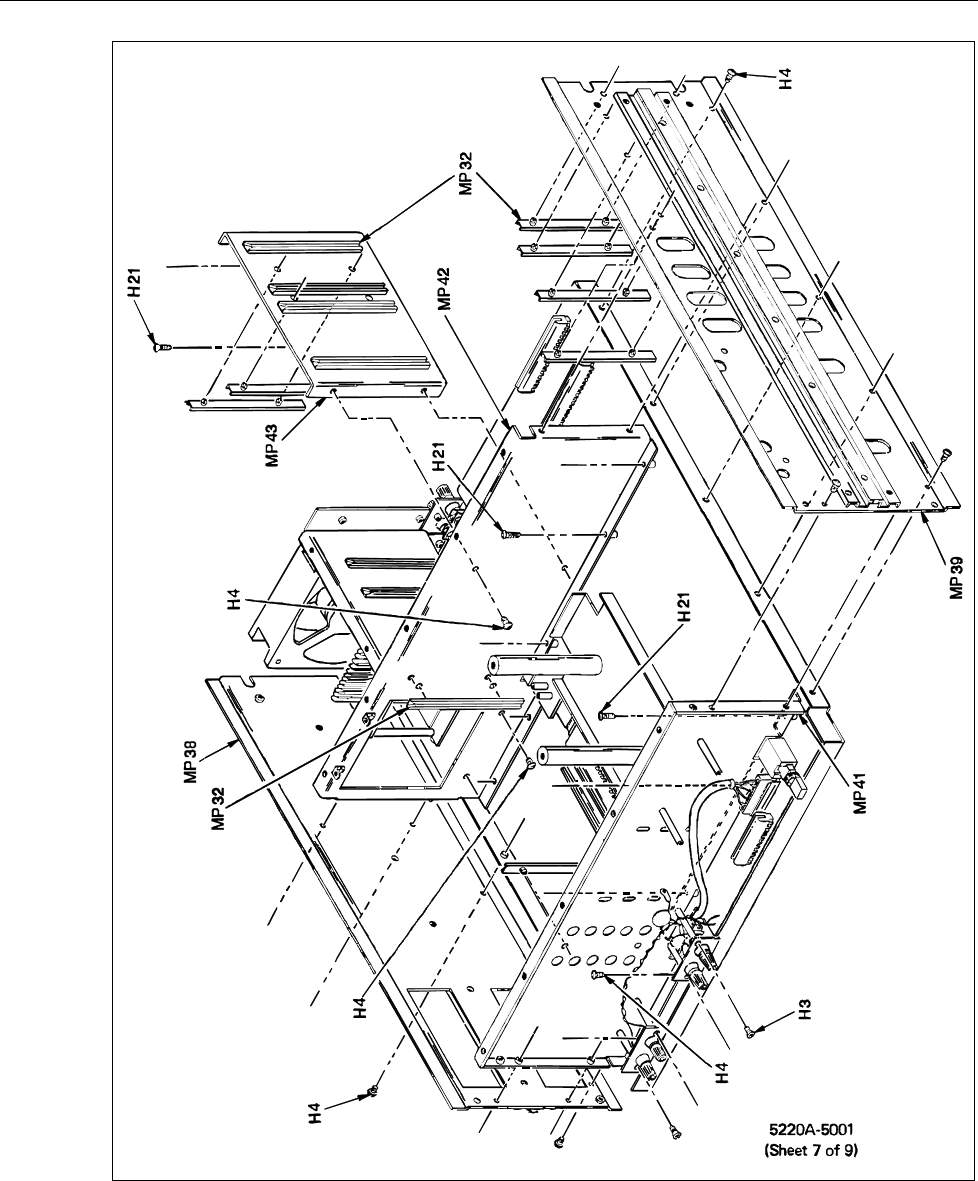
5220A
Instruction Manual
5-14
ajs26f.wmf
Figure 5-1. 5220A Final Assembly (cont.)
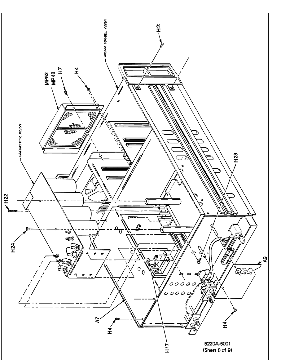
List of Replaceable Parts
Service Centers
5
5-15
ajs27f.wmf
Figure 5-1. 5220A Final Assembly (cont.)
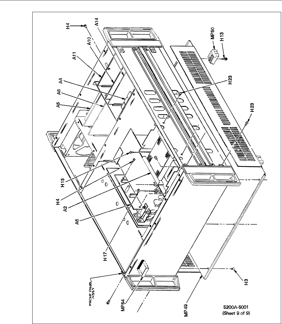
5220A
Instruction Manual
5-16
ajs28f.wmf
Figure 5-1. 5220A Final Assembly (cont.)
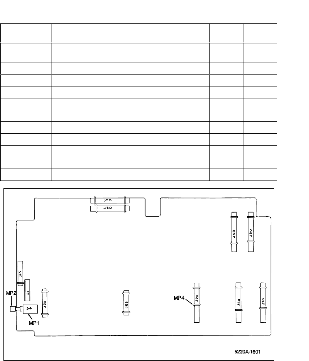
List of Replaceable Parts
Service Centers
5
5-17
Table 5-2. A1 Motherboard PCB Assembly
Reference
Designator Description
Fluke
Part No.
Total
Quantity
J10, J20, J30,
J40, J50, J70, J90
Connector, PCB Edge, Rec., 0.150 CTR, 40 Position 422550 7
J1 Header, 1 Row, 0.156 CTR, 10 Pin 446724 1
J10, J85 Connector, PCB Edge, Rec., 0.150 CTR, 24 Position 295352 2
J80 Connector, PCB Edge, Rec., 0.150 CTR, 22 Position 459883 1
MP1 Cover, AC Switch 475681 1
MP2 Pushbutton, SML Rect. C L Repl., Green 419747 1
MP3 Pin, Single, PCB, 0.025 Sq. 267500 3
MP4 Connector, Accessory, PCB Edge, Polarizing Insert 424572 19
MP5 Bushing, Snap-In, Nylon, 0.250 ID 102996 2
MP6 Spacer, Swaged, Round, Brass, 6-32 x 0.500 284380 4
S4 Switch, On-Off 453605 1
ajs35f.wmf
Figure 5-2. A1 Motherboard PCB Assembly
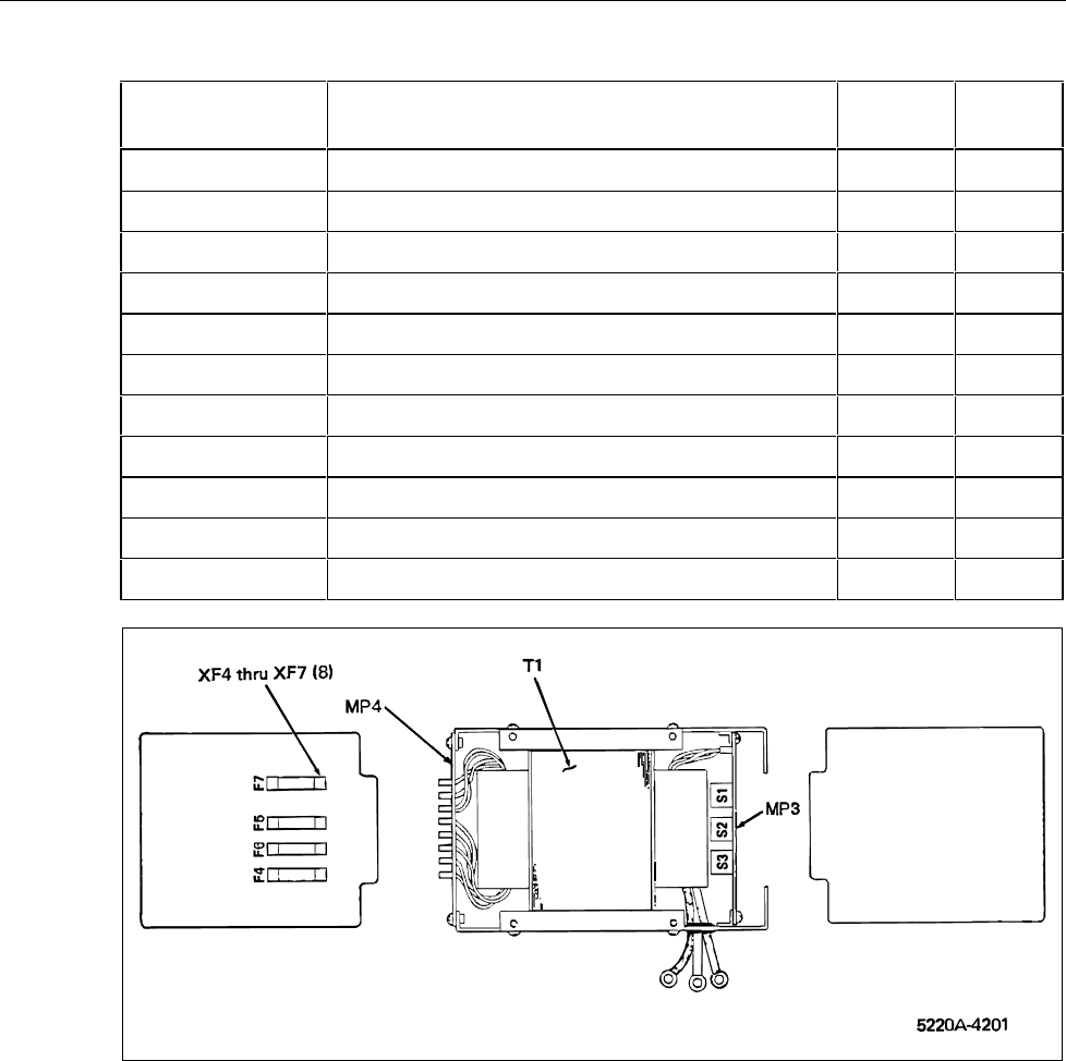
5220A
Instruction Manual
5-18
Table 5-3. A2 Power Transformer Assembly
Reference
Designator Description
Fluke
Part No.
Total
Quantity
F4 – F7 Fuse, 0.25 x 1.25, 0.5 A, 250 V, Slow 109322 4
H1 Screw, Machine, PH, P, Steel, 8-32 x 0.250 228890 8
H2 Screw, Machine, PH, P, Steel, 6-32 x 0.250 152140 8
MP1 Transformer Plate, Inboard 489468 1
MP2 Transformer Plate, Outboard 489476 1
MP3 Forward Transformer Terminator Assembly 660217 1
MP4 Aft Transformer Terminator Assembly 660225 1
MP5 Grommet, Slot, Rubber, 0.750, 0.875 380782 1
S1–S3 Switch, Slide, DPDT, Power 234278 3
T1 Power Transformer 477000 1
XF4–XF7 Fuse, Clip, PCB, 1/4 x 1-1/4 756460 8
ajs37f.wmf
Figure 5-3. A2 Power Transformer Assembly

List of Replaceable Parts
Service Centers
5
5-19
Table 5-4. A3 Capacitor Bus PCB Assembly
Reference
Designator Description
Fluke
Part No.
Total
Quantity
C1 – C8 Capacitor, AL, 50,000 µF, +100-10 %, 15 V, Hi Term 432525 8
CR1, CR3 Diode, SI, 50 PIV, 20.0 A 483206 2
CR2, CR4 Diode, SI, 50 PIV, 20.0 A 483214 2
F2, F3 Fuse, 0.25 x 1.25, 30 A, 32 V, Fast 500793 2
H14 Nut, Machine, Hex, BR, ¼-28 110619 9
H15 Washer, Shoulder, Fiber, 0.250 ID 110833 4
H16 Screw, Machine, PH, P, Steel, 10-32 x 0.375 159749 5
H17 Nut, Machine, Hex, Steel, 8-32 110544 10
H18 Screw, Machine, PH, P, Steel, 10-32 x 0.375 114314 16
H19 Washer, Flat, Steel, 0.265, 0.500, 0.031 110718 4
H20 Washer, Flat, Teflon, 0.366 x 0.266 x 0.050 543314 4
MP35 Heatsink, Diode 502179 1
MP36 Insulation Part, Diode, Silicone, Washer 500785 4
MP37 Bus, Capacitor 497982 1
R2, R5 Resistor, CC, 100, ±10 %, 2 W 109934 2
XF2, XF5 Fuse, Clip, PCB, 1/4 x 1-1/4 756460 4
5220A
Instruction Manual
5-20
ajs38f.wmf
Figure 5-4. A3 Capacitor Bus PCB Assembly

List of Replaceable Parts
Service Centers
5
5-21
Table 5-5. A4 Regulator PCB Assembly
Reference
Designator Description
Fluke
Part No.
Total
Quantity
C9, C10, C16, C17 Capacitor, AL, 4700 µF, +75-20 %, 16 V 379370 4
C11, C14, C15, C18 Capacitor, TA, 22 µF, ±20 %, 25 V 357780 4
C12, C13 Capacitor, AL, 2200 µF, +75-20 %, 25 V 392720 2
CR5 – CR7 Diode, SI, Rectifier, Bridge, BV = 100 V, IO = 1.0 A 392910 3
CR8, CR9 h Diode, SI, BV = 75 V, IO = 150 mA, 500 mW 203323 2
H1 Screw, Machine, PH, P, SEMS, Steel, 4-40, 0.250 185918 4
H2 Nut, Machine, Hex, Steel, 4-40 110635 4
MP1 Heat Dissipator, PCB MTG, 1.380, 2.000, 0.500 386235 4
MP2 Cable Tie, 4.0 L, 0.100 W, 0.75 Dia. 172080 6
R4, R6, R9, R15 Resistor, CF, 100 k, ±5 %, 0.25 W 348920 4
R7, R12 Resistor, CC, 220 Ω, ±10 %, 1 W 109462 2
R8 Resistor, CF, 1 k, ±5 %, 0.25 W 343426 1
R10, R11 Resistor, CC, 1 k, ±10 %, 1 W 109371 2
R13 Resistor, CF, 18 k, ±5 %, 0.25 W 348862 1
TP1 – TP8 Terminal, Uninsulated, Feedthrough, Hole, Turret 179283 8
U1, U4 h IC, Voltage Regulator, Fixed, +5 V, 1.5 A 355107 2
U2 h IC, Voltage Regulator, Fixed, +15 V, 1.5 A 413187 1
U3 h IC, Voltage Regulator, Fixed, -15 V, 1.5 A 413179 1
VR1 h Zener, Uncompensated, 4.3 V, 5 %, 20.0 mA, 0.4 W 180455 1
h Indicates a static-sensitive part.
5220A
Instruction Manual
5-22
ajs39f.wmf
Figure 5-5. A4 Regulator PCB Assembly

List of Replaceable Parts
Service Centers
5
5-23
Table 5-6. A5 Preamplifier PCB Assembly
Reference
Designator Description
Fluke
Part No.
Total
Quantity
C1, C2 Capacitor, CER, 100 pF, ±2 %, 100 V, COG 512848 2
C3, C5, C6 Capacitor, CER, 0.22 µF, ±20 %, 50 V, Z5U 309849 7
C4 Capacitor, Variable,1 – 42 pF, 750 V, Glass 758029 1
C7 Capacitor, CER, 1800 pF, ±5 % 50 V, COG 528547 1
C12, C15 Capacitor, TA, 10 µF, ±20 %, 20 V 330662 2
CR1, CR2, CR6 h Diode, SI, BV = 75 V, IO = 150 mA, 500 mW 203323 3
CR3 – CR5 h Diode, SI, BV = 20.0 V, IO = 50 mA, 250 mW 375907 3
E1, E2, E3 Jumper, Wire, Non-insulated, 0.200 CTR 816090 3
H1 Screw, Machine, SEMS, PH, P, Steel, 6-32, 0.250 178533 4
K1, K2 Relay, Reed, 1 Form A, 4.5 V dc 424408 2
MP1 Spacer, Swaged, Round, Brass, 6-32 x 0.812 306804 4
MP2 Shield, Preamplifier 486001 1
MP3 Spacer, Switch Standoff, Polyethylene, 0.094 285353 2
Q1 h Transistor, SI, N-JFET, Hi-Voltage, TO-92 393314 1
Q2 h Transistor, SI, NPN, Dual, TO-5 478099 1
Q3 h Transistor, SI, NPN, Small Signal 329698 1
R1, R2 Resistor Set, 1 k; 98.5 k 502625 1
R3 Resistor, Variable, CER, 500 Ω, ±20 %, 0.5 W 267849 1
R4 Resistor, MF, 60.4 k, ±1 %, 0.125 W, 100 PPM 291419 1
R5, R7 Resistors, 301 k Set 502671 1
R6 Resistor, Variable, CER, 2 k, ±20 %, 0.5 W 267864 1
R8 Resistor, MF, 215 k, ±1 %, 0.125 W, 100 PPM 289470 1
R9 Resistor, MF, 1 k, ±, 0.125 W, 100 PPM 168229 1
R10, R20 Resistor, CF, 100 k, ±5 %, 0.25 W 348920 2
R11, R121Resistor, MF, 100.03 k, ±0.1 %, 0.125 W, 25 PPM 291088 1
R132Resistor, Factory Selected - 2
R14 Resistor, MF, 100k, ±1 %, 0.125 W, 100 PPM 248807 1
R15, R25 Resistor, MF, 392 Ω, ±1 %, 0.125 W, 100 PPM 260299 2
R16 Resistor, MF, 10 k, ±1 %, 0.125 W, 100 PPM 168260 1
R17, R18 Resistor, CF, 10 Ω, ±5 %, 0.25 W 340075 2
5220A
Instruction Manual
5-24
Table 5-6. A5 Preamplifier PCB Assembly (cont.)
Reference
Designator Description
Fluke
Part No.
Total
Quantity
R19 Resistor, MF, 422 Ω, ±1 %, 0.125 W, 100 PPM 288506 1
R21, R23 Resistor, CF, 1 k, ±5 %,, 0.25 W 343426 2
R22 Resistor, CF, 1.2 k, ±5 %, 0.25 W 441378 1
R24 Resistor, CF, 33k, ±5 %, 0.25 W 348888 1
TP1 – TP14 Terminal, Un-insulated, Feed-through, Hole, Turret 179283 14
U1 h IC, Array, 5 Transistors, NPN, 3 Isolated, 2
Differentially Connected
248906 1
U2 h IC, OP AMP, JFET Input, TO-5 429837 1
U3 h Isolator, Opto, LED to Photo Resistor 507475 1
U4 h IC, CMOS, Hex Inverter 404681 1
h Indicates a static-sensitive part.
1. R11 and R12 are factory selected. See Table 4-4.
2. R13 may or may not be installed as factory selected. See Table 4-5.
List of Replaceable Parts
Service Centers
5
5-25
ajs40f.wmf
Figure 5-6. A5 Preamplifier PCB Assembly

5220A
Instruction Manual
5-26
Table 5-7. A6 Driver PCB Assembly
Reference
Designator Description
Fluke
Part No.
Total
Quantity
C1 Capacitor, Polyester, 0.027 µF, ±10 %, 250 V 267120 1
C2 Capacitor, TA, 6.8 µF, ±20 %, 35 V 363713 1
C3, C4 Capacitor, CER, 180 pF, ±10 % 1000 V, S3N 105890 2
C5 Capacitor, CER, 5000 pF, ±20 %, 100 V, Z5V 175232 1
C6 Capacitor, TA, 220 µF, ±20 %, 6 V 408682 1
C7 Capatitor, CER, 0.1 µF, ±20 %, 100 V Z5V 149146 1
CR1 h Diode, SI, N-JFET, Current Regulator, IF = 5.3 mA 334714 1
CR2 h Diode, SI, BV = 75 V, IO = 150 mA, 500 mW 203323 1
H1 Screw, Machine, PH, P, Steel, 6-32 x 1.000 114215 1
H2 Nut, Hex, Steel, 6-32 110551 1
MP1 Spacer, Round, Aluminum, 0.156 ID x 0.750 100966 1
Q1 h Transistor, SI, PNP, Small Signal 229898 1
Q2 – Q4 h Transistor, SI, NPN, Small Signal 218081 3
Q5, Q9, Q10 h Transistor, SI, PNP, Small Signal 402586 3
Q6, Q7, Q11 h Transistor, SI, N-JFET, TO-92, Switch 261578 3
Q8, Q12 h Transistor, SI, NPN, Small Signal 346916 2
R1 – R3 Resistor, CF, 1 k, ±5 %, 0.25 W 343426 3
R4, R5 Resistor, MF, 523 Ω, ±1 %, 0.125 W, 100 PPM 294835 2
R6 Resistor, Variable, CERM, 10 Ω, ±20 %, 0.5 W 344135 1
R7, R23 Resistor, CF, 100 k, ±5 %, 0.25 W 348920 2
R8 Resistor, MF, 191 Ω, ±1 %, 0.125 W, 100 PPM 325639 1
R9, R12 Resistor, CF, 560 Ω, ±5 %, 0.25 W 385948 2
R10 Resistor, 240 Ω, ±5 %, 0.25 W 376624 1
R13 Resistor, Variable, CERM, 100 Ω, ±20 % , 0.5 W 267823 1
R14, R16 Resistor, MF, 604 Ω, ±1 %, 0.125 W, 100 PPM 320309 2
R15 Resistor, MF, 383 Ω, ±1 %, 0.125 W, 100 PPM 375899 1
R17 Resistor, MF, 953 Ω, ±1 %, 0.125 W, 100 PPM 288555 1
R18, R24 Resistor, MF, 100 Ω, ±1 %, 0.125 W, 100 PPM 168195 2
R19, R25 Resistor, CF, 51 Ω, ±5 %, 0.25 W 414540 2
R20 Resistor CF, 100 Ω, ±5 %, 0.25 W 348771 1
R21, R22 Resistor, MF, 33.2 Ω, ±1 %, 0.125 W, 100 PPM 296681 2
R26, R27 Resistor, MF, 20 Ω, ±1 %, 0.125 W, 100 PPM 236844 2
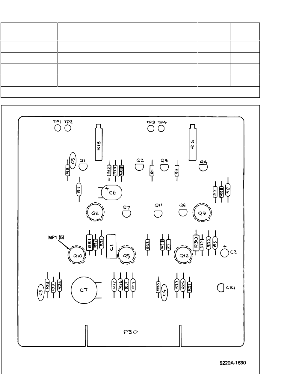
List of Replaceable Parts
Service Centers
5
5-27
Table 5-7. A6 Driver PCB Assembly (cont.)
Reference
Designator Description
Fluke
Part No.
Total
Quantity
R28, R29 Resistor, CF, 6.8 k, ±5 %, 0.25 W 368761 2
R30, R31 Resistor, CC, 10 Ω, ±10 %, 0.5 W 108092 2
TP1 – TP4 Terminal, Un-insulated, Feed-through, Hole, Turret 179283 4
VR1, VR2 h Zener, Uncompensated, 4.3 V, 5 %, 20.0 mA, 0.4 W 180455 2
h Indicates a static-sensitive part.
ajs41f.wmf
Figure 5-7. A6 Driver PCB Assembly

5220A
Instruction Manual
5-28
Table 5-8. A7 Output PCB Assembly
Reference
Designator Description Fluke
Part No. Total
Quantity
H1 Screw, Machine, PH, P, Steel, 4-40 x 0.375 152124 2
H2 Washer, Lock, Internal, Steel, #4 110403 2
H3 Nut, Hex, S. Steel, 4-40 147611 2
H4 Screw, Machine, PH, P, Steel, 6-32 x 0.250 152140 2
H5 Screw, Machine, PH, P, Steel, 6-32 x 0.750 114223 8
H6 Washer, Lock, Internal, Steel #6 110338 1
H7 Nut, Hex, Steel, 6-32 110551 1
H8 Screw, Machine, PH, P, Steel, 8-32 x 0.35 114124 8
H9 Nut, Macine, Hex, Steel, 8-32 110544 2
H10 Screw, Machine, PH, P, Steel, 4-40 x 0.312 152116 1
MP1 Output, PCB Bracket 489567 1
MP2 Fin, Heatsink 489880 1
MP3 Plate, Temperature Sense 489898 1
MP4 Bus, Output PCB 502161 2
MP5 Output Chamber 485961 1
MP6 Defector Fin, Heatsink 489508 1
MP7 Spacer, Swaged, Hex, Brass, 6-32 x 0.625 181727 2
MP8 Spacer, Swaged, Round, Brass, 6-32 x 0.187 351882 8
MP9 Insulated Part, Transistor, Aluminum, TO-3 477802 4
MP10 Socket, Single, PCB, For 0.018 – 0.040 Pin 348201 8
MP11 Heat Dissipator, W/BEO Washer, TO-5 407262 1
MP12 Space, Transistor Mount, DAP 152207 1
MP13 Washer, Flat, Nylon, 0.257 ID x 0.500 x 0.093 682385 1
MP14 Plastic Part, Hole Plug, Polyethylene, 0.312 187799 2
MP15 Washer, Shoulder, Nylon, 0.113, 0.345 485417 3
MP16 Insulated Part, Transistor, Film, TO-220 412809 1
Q101 h Transistor, SI, BV = 45 V, 27 W, TO-220 325753 1
Q102 h Transistor, SI, BV = 45 V, 30 W, TO-220 325761 1
Q103, Q104 h Transistor, SI, BV = 60 V, 200 W, TO-3 483222 2
Q105, Q106 h Transistor, SI, PNP, Small Signal 483230 2
Q107 Resistor, CF, 1 k, ±5 %, 0.25 W 402586 1
R101 – R107 Resistor, CF, 1 k, ±5 %, 0.25 W 343426 7
R108, R109 Resistor, CC, 5.1 Ω, ±5 %, 0.5 W 177147 2
R110 – R113 Resistor, 0.086 Ω, ±1 %, 4-Terminal, 10 W, 50 PPM 490771 4
R114, R115 Resistor, WW, 2.4 Ω, ±5 %, 2 W 219337 2
S101 Thermo, NO230±8F, NC200±8F, 15 A/120 V ac 344002 1
TP1 – TP7 Terminal, Un-insulated, Feed-through, Hole, Turret 179283 7
XQ101, XQ102 Socket, Transistor, 3-Pin 402958 2
h Indicates a static-sensitive part.
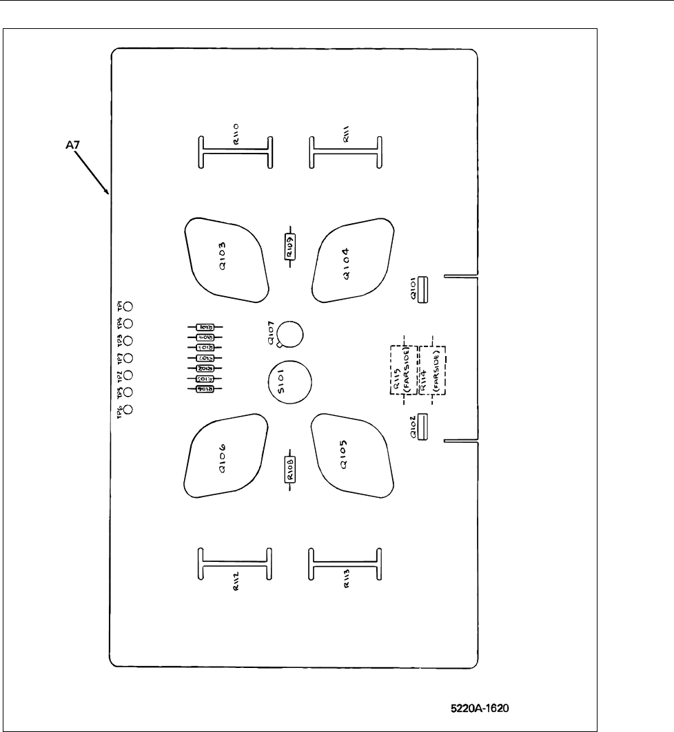
List of Replaceable Parts
Service Centers
5
5-29
ajs42f.wmf
Figure 5-8. A7 Output PCB Assembly
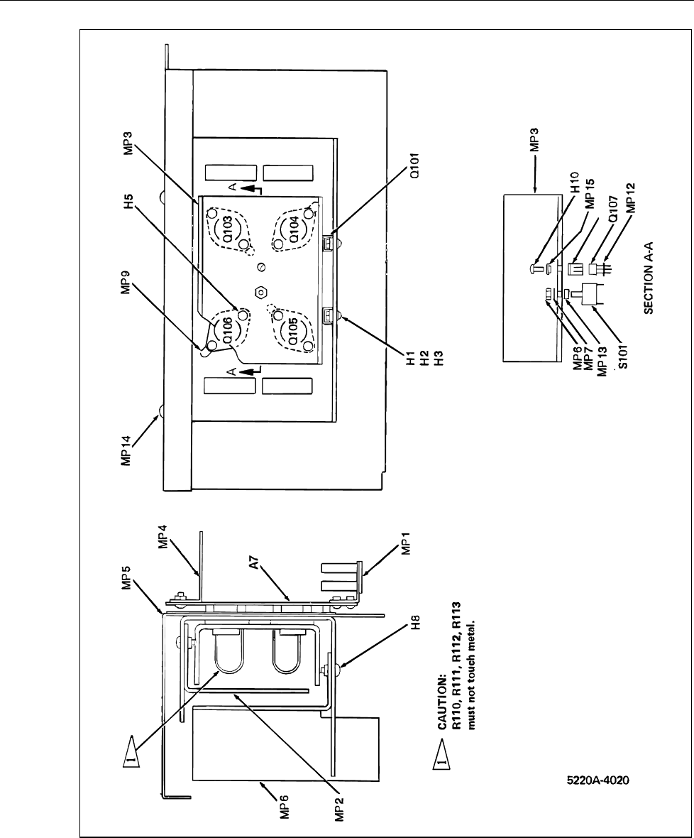
5220A
Instruction Manual
5-30
ajs43f.wmf
Figure 5-8. A7 Output PCB Assembly (cont.)

List of Replaceable Parts
Service Centers
5
5-31
Table 5-9. A8 Analog Control PCB Assembly
Reference
Designator Description
Fluke
Part No.
Total
Quantity
C1 Capacitor, CER, 0.10 µF, ±20 %, 50 V, X7R 853650 1
C2 Capacitor, Polyester, 0.22 µF, ±10 %, 100 V 436113 1
C3 Capacitor, TA, 0.68 µF, ±10 %, 35 V 182790 1
CR1 – CR10 h Diode, SI, BV = 20.0 V, IO = 50 Machine, Selected IR 348117 10
CR11 h Diode, SI, BV = 75.0 V, IO = 150 Machine, 500 mW 203323 1
Q1, Q3 h Transistor, SI, PNP, Small Signal 195974 2
Q2, Q4 h Transistor, SI, NPN, Small Signal 218396 2
R1, R2 Resistor, MF, 100 k, ±1 %, 0.125 W, 100 PPM 248807 2
R3 Resistor, CF, 51 k, ±5 %, 0.25 W 376434 1
R4, R6, R7, R16 –
R19, R25, R28,
R29, R32
Resistor, CF, 10 k, ±5 %, 0.25 W 348839 11
R5, R10, R27, R31,
R35 – R42
Resistor, CF, 100 k, ±5 %, 0.25 W 348920 12
R8 Resistor, CF, 82 k, ±5 %, 0.25 W 348912 1
R9 Resistor, Variable, CER, 100 k, ±10 %, 0.5 W 288308 1
R11 Resistor, CF, 300 k, ±5 %, 0.25 W 441535 1
R12, R24, R43 Resistor, CF, 1 k, ±5 %, 0.25 W 343426 3
R13, R14 Resistor, MF, 10 k, ±1 %, 0.125 W, 100 PPM 168206 2
R15 Resistor, CF, 5.1 k, ±5 %, 0.25 W 368712 1
R20 Resistor, CF, 9.1 k, ±5 %, 0.25 W 441691 1
R21 Resistor, Variable, CER, 5 k, ±10 %, 0.5 W 288282 1
R22 Resistor, CF 1.1 k, ±5 %, 0.25 W 348797 1
R23 Resistor, CF, 390 k, ±5 %, 0.25 W 742475 1
R26, R30 Resistor, CF, 22 k, ±5 %, 0.25 W 348870 2
R33 Resistor, CF, 1.2 k, ±5 %, 0.25 W 441378 1
TP1 – TP5, TP7 –
TP13
Terminal, Un-insulated, Feed-through, Hole, Turret 179283 12
U1, U2 h IC, Op Amp, Quad, 14-Pin DIP 402669 2
U3 h IC, LSTTL, Hex Inverter w/Schmitt Trigger 483180 1
VR1, VR2 h Zener, Uncompensated, 6.8 V, 10 %, 1.0 Machine, 0.4 W 187195 2
h Indicates a static-sensitive part.
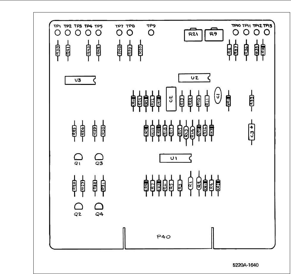
5220A
Instruction Manual
5-32
ajs44f.wmf
Figure 5-9. A8 Analog Control PCB Assembly
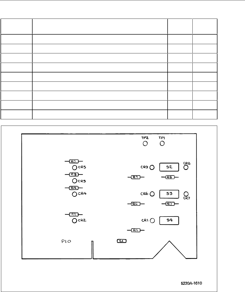
List of Replaceable Parts
Service Centers
5
5-33
Table 5-10. A9 Front Panel PCB Assembly
Reference
Designator Description
Fluke
Part No.
Total
Quantity
C1 Capacitor, CER, 0.22 µF, ±20 %, 50 V, Z5U 309849 1
DS1 – DS9 LED, Red, PCB mount, Luminous Intensity = 0.5 MCD 369777 9
MP1 Cover, Pushbutton, Switch 401299 3
MP2 Switch Part, SPST, Spring 414516 3
MP3 Switch Part, SPST, Fixed Contact 416875 3
MP4 Pushbutton-Square-, Dark Putty Grey 406728 3
R1 – R9 Resistor, CF, 220 Ω, ±5 %, 0.25 W 342626 9
S1 – S3 Actuator, Switch 412106 3
TP1 – TP2 Terminal, Un-insulated, Feed-through, Hole, Turret 179283 2
ajs29f.wmf
Figure 5-10. A9 Front Panel PCB Assembly

5220A
Instruction Manual
5-34
Table 5-11. A10 Logic PCB Assembly
Reference Designator Description Fluke
Part No. Total
Quantity
C1, C3, C4 Capacitor, Mica, 100 pF, ±5 %, 500 V 148494 3
C2 Capacitor, TA, 4.7 µF, ±20 %, 25 V 161943 1
C5 Capacitor, TA, 2.2 µF, ±20 %, 20 V 161927 1
C6 – C8 Capacitor, TA, 1 µF, ±10 %, 35 V 161919 3
C9 Capacitor, TA, 22 µF, ±20 %, 15 V 423012 1
C10 – C14 Capacitor, CER, 0.22 µF, ±20 %, 50 V, Z5U 309849 5
C15 Capacitor, CER, 0.01 µF, +80-20 %, 100 V, Z5V 149153 1
C16 Capacitor, TA, 0.47 µF, ±20 %, 35 V 161349 1
CR1 – CR3 h Diode, SI, BV = 75 V, IO = 150 mA, 500 mW 203323 3
R1, R2, R9, R10, R15, R16,
R19 Resistor, CF, 220 Ω, ±5 %, 0.25 W 342626 7
R3 – R6, R8, R11, R12, R14,
R17, R18, R20, R21 Resistor, CF, 10 k, ±5 %, 0.25 W 348839 12
R7, R22 Resistor, CF, 47 k, ±5 %, 0.25 W 348896 2
R13, R24, R26 Resistor, CF, 100 k, ±5 %, 0.25 W 348920 3
R22 Resistor, CF, 10 k, ±5 %, 0.25 W 348839 1
R23, R25 Resistor, CF, 4.7 k, ±5 %, 0.25 W 348821 2
TP1, TP2 Terminal, Un-insulated, Feed-through, Hole,
Turret 179283 2
U1, U4, U5, U20 Isolator, Opto, LED to Transistor, Dual 454330 4
U2 h IC, CMOS, Quad, 2-Input NAND w/Schmitt
Trigger
404632 1
U3 h IC, CMOS, Hex Inverter 404699 1
U6, U19 h IC CMOS, Quad 2-Input AND Gate 408401 2
U7, U10 h IC, CMOS, Dual D F/F, + Edge Trigger 418830 2
U8, U11 h IC, CMOS, Retrigger/Reset Multivibrator 393512 2
U9 h IC, CMOS, Triple 3-Input NOR Gate 355180 1
U12 – U14 h IC, LSTTL, Quad 2-Input NAND Gate 393116 3
U15 h IC, TTL, Dual NAND Driver w/Open Collector 329706 1
U16, U17 h IC, CMOS, Dual D F/F, + Edge Trigger 340117 2
U21 h IC, CMOS, Triple 3-Input OR Gate 408575 1
U22 h IC, LSTTL, 4-Bit Parallel I/O Right and Left
Shift Register
393249 1
U23 h IC, Bipolar, Timer, 8-Pin, DIP 402610 1
XU23 Socket, IC, 8-Pin 478016 1
h Indicates a static-sensitive part.
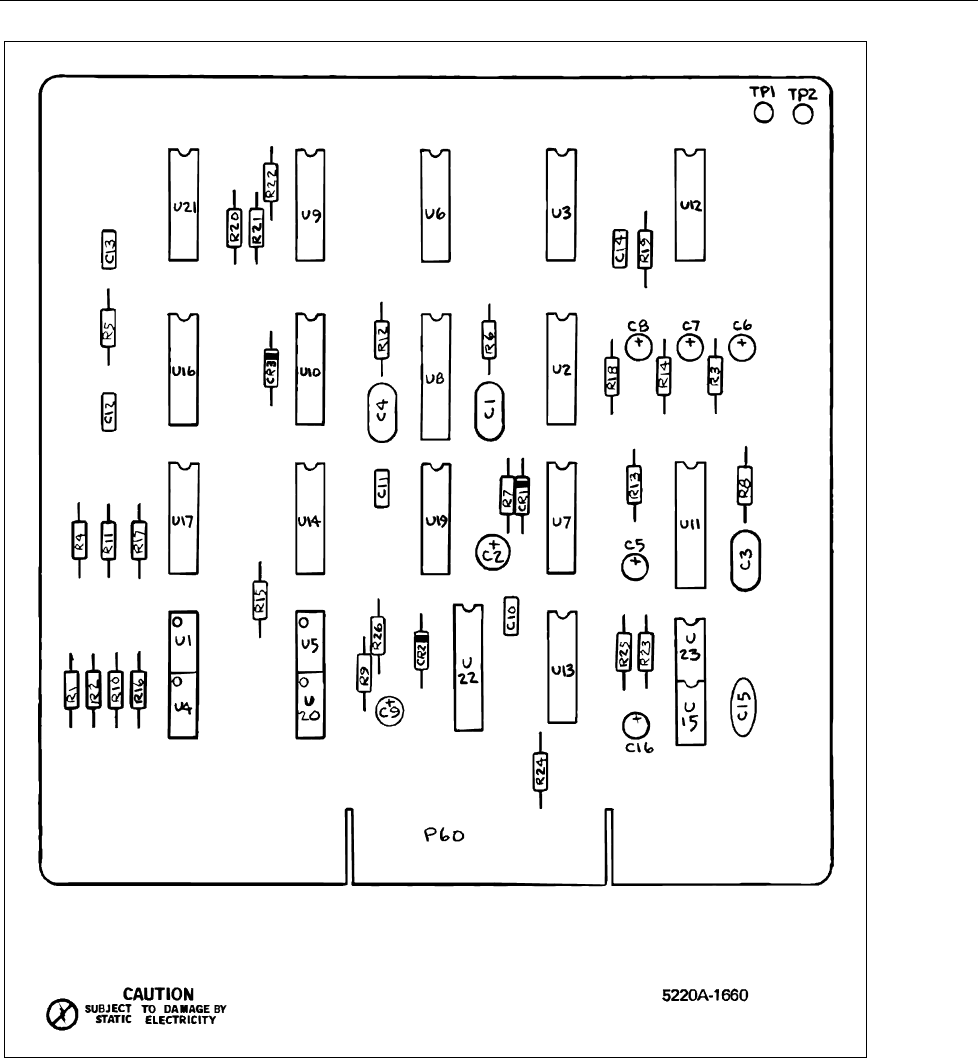
List of Replaceable Parts
Service Centers
5
5-35
ajs30f.wmf
Figure 5-11. A10 Logic PCB Assembly

5220A
Instruction Manual
5-36
Table 5-12. A11 MIS Bus Interface PCB Assembly
Reference
Designator Description
Fluke
Part No.
Total
Quantity
C1 Capacitor, TA, 4.7 µF, ±20 %, 25 V 161943 1
C2 Capacitor, TA, 22 µF, ±20 %, 15 V 423012 1
C3, C4 Capacitor, CER, 0.22 µF, ±20 %, 50 V, Z5U 309849 2
CR1 h Diode, SI, BV = 75.0 V, IO = 150 mA, 500 mW 203323 1
H1 Screw, Machine, PH, P, SEMS, Steel, 4-40, 0.250 185918 2
J71 Connector, Micro-Ribbon, REC, PCB, 24 Position 441337 1
MP1 Connector ACC, Micro-Ribbon, Latch 412700 2
MP2 Connector ACC, Micro-Ribbon, Spring 412718 2
MP3 Spacer, Swaged, Round, Brass, 4-40 x 0.187 335604 2
MP4 Spacer, Swaged, Round, Brass, 6-32 x 0.570 261875 1
R1 – R12 Resistor, CF, 10 k, ±5 %, 0.25 W 348839 12
R14 – R22 Resistor, CF, 1 k, ±5 %, 0.25 W 343426 9
R23 Resistor, CF, 47 k, ±5 %, 0.25 W 348896 1
TP1 – TP2 Terminal, Un-insulated, Feed-through, Hole, Turret 179283 2
U1 h IC, CMOS, Quad D F/F, + Edge Trigger, w/Clear 452912 1
U2 – U7 h IC, LSTTL, Quad 2-Input NAND Gate 394205 2
U3 h IC, CMOS, Hex Inverter 404699 1
U4 h IC, CMOS, Quad 2-Input NAND Gate 418509 1
U5 h IC, CMOS, Triple 3-Input NAND Gate 418244 1
U6 h IC, LSTTL, Quad 2-Input NAND Gate 393116 1
h Indicates a static-sensitive part.
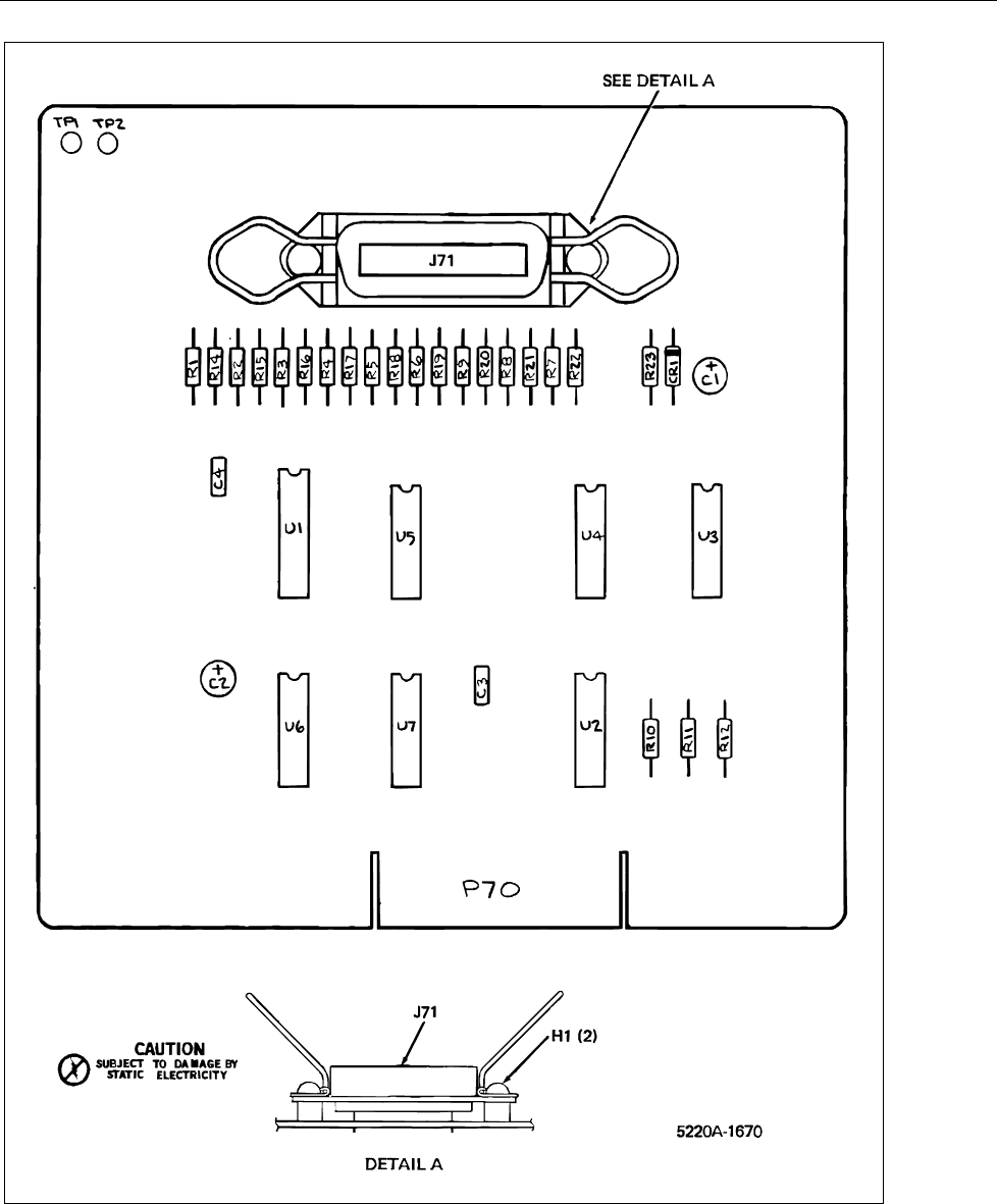
List of Replaceable Parts
Service Centers
5
5-37
ajs31f.wmf
Figure 5-12. A11 MIS Bus PCB Assembly

5220A
Instruction Manual
5-38
Note
The A12 shunt assembly is a suggested non-repairable assembly.
Table 5-13. A12 Shunt Assembly
Reference
Designator Description
Fluke
Part No.
Total
Quantity
H1 Screw, Machine, SEMS, PH, P, Steel, 6-32 x 0.500 177030 4
H2 Screw, Machine, RH, SL, Steel, 6-32 x 2.750 115022 4
H3 Nut, Mini, Hex, SS, 6-32 110569 4
H4 Solder, Tin-Lead Alloy, Preform Ring 516989 32
J1 – J4 Banana Plug, Panel 101543 4
MP1 Top Support, Shunt 489906 1
MP2 Bottom Support, Shunt 489914 1
MP3 Terminal, Shunt 489922 2
MP4 Element, Shunt 524397 16
MP5 Spacer, Round, Aluminum, 0.156 ID x 0.156 157792 4
MP6 Spacer, Round, Aluminum, 0.156 ID x 1.500 104257 4
MP7 Spacer, Round, Aluminum, 0.156 ID x 1.000 102905 4
W1 Cable, Shunt 502674 1
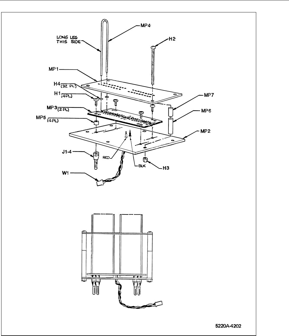
List of Replaceable Parts
Service Centers
5
5-39
ajs32f.wmf
Figure 5-13. A12 Shunt Assembly
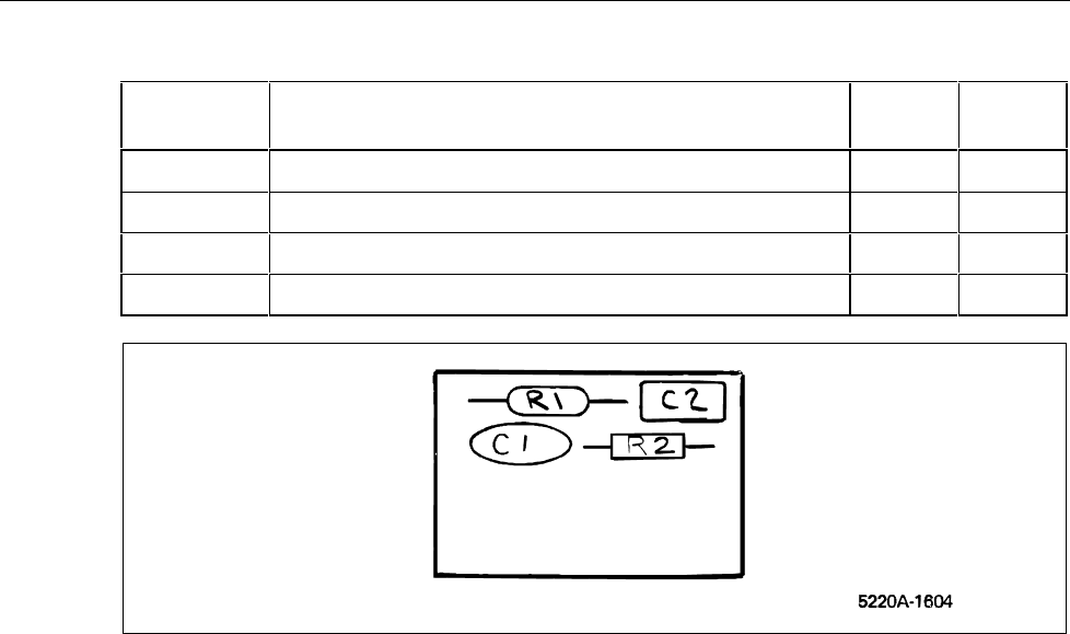
5220A
Instruction Manual
5-40
Table 5-14. A13 Output Termination PCB Assembly
Reference
Designator Description
Fluke
Part No.
Total
Quantity
C1 Capacitor, CER, 0.025 µF, 20 %, 100 V, Z5W 168435 1
C2 Capacitor, CER, 0.1 µF, +80-20 %, 25 V, Z5U 369199 1
R1 Resistor, MF, 40.2, ±1 %, 0.125 W, 100 PPM 245373 1
R2 Resistor, CF, 10 Ω, ±5 %, 0.25 W 340075 1
ajs33f.wmf
Figure 5-14. A13 Output Termination PCB
List of Replaceable Parts
Service Centers
5
5-41
Table 5-15. A14 Extender PCB Assembly
Reference
Designator Description
Fluke
Part No.
Total
Quantity
H1 Screw, Machine, SEMS, PH, P, Steel, 6-32, 0.250 178533 4
H2 Rivet, S-Tub, Oval, Steel, 0.118 x 0.218 103606 2
J1 Connector, PCB Edge, REC, 0.150 CTR, 40 Position 422550 1
J2 Connector, ACC, PCB Edge, Polarizing Insert 424572 1
MP1 Bracket, Right Angle, Tapped, Brass, 6-32 404525 4
ajs34f.wmf
Figure 5-15. A14 Extender PCB Assembly

5220A
Instruction Manual
5-42
6-1
Section 6
Option and Accessory Information
6-1. Introduction
This section of the manual documents the options and accessories available for use with
the 5220A. Currently, there are no options, and the accessories are limited to a choice of
two rack-mounting kits and a precision current shunt for calibration purposes. Each is
described in the following accessories subsection.
6-2. Accessories
6-3. Rack Mounting Kit (M08-205-600)
The 5220A can be rack mounted in a standard 19-inch equipment rack using Rack
Mounting Kit M08-205-600. Use the following procedure to install the kit:
1. Peel off the name plate decals from the front side corners of theinstrument.
2. Remove the front corner screws that match the hole pattern in the rack mounting ears
(see Figure 6-1).
3. Attach the rack mounting ears to the front corners of the unit using the screws
supplied in the rack mounting kit.
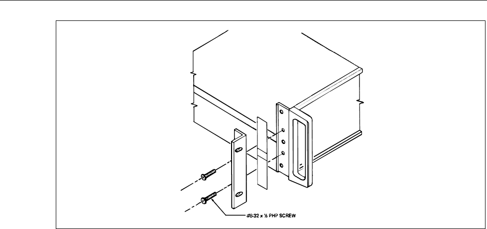
5220A
Instruction Manual
6-2
ajs45f.wmf
Figure 6-1. Rack Mounting Kit

Option and Accessory Information
Accessories
6
6-3
6-4. Rack Slide Kit (M00-280-610)
The 5220A can be rack mounted in a 24-inch deep equipment rack using the Rack Slide
Kit, model M00-280-610. Use the following procedure to install the kit:
1. Remove the horizontal side trim decal from both sides of the instrument.
2. Refer to Figure 6-2. Using the screws supplied with the kit, attach the chassis section
(B) of the slide kit to each side of the unit. Use the center row of mounting holes.
3. Install the cabinet section (D) of the center section (C) in the equipment rack.
4. Pull the center section of the slide out through the front of the equipment rack until it
locks in the extended position.
5. Depress the spring locks on the chassis section (B) and join sections B and C.
6. Push the instrument into the equipment rack and then pull it out to the extended
position. The spring locks should limit the rack slide travel.
6-5. Precision Y5020A Current Shunt
The Model Y5020A is a precision, high-current shunt recommended for use in calibrating
the Model 5220A Transconductance Amplifier. An instruction manual is suppled with the
unit.
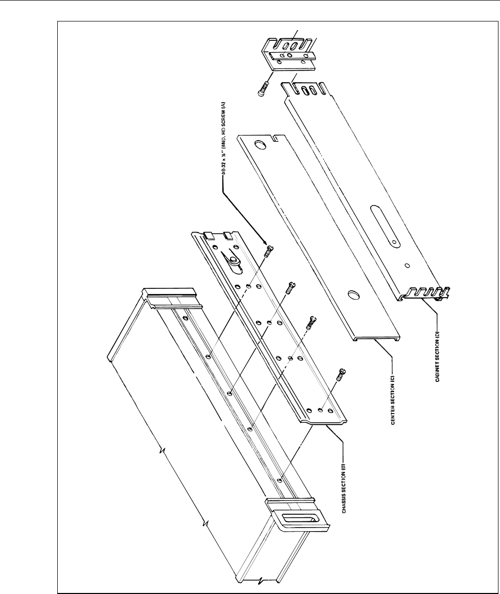
5220A
Instruction Manual
6-4
ajs46f.wmf
Figure 6-2. Rack Slide Kit
7-1
Chapter 7
Schematic Diagrams
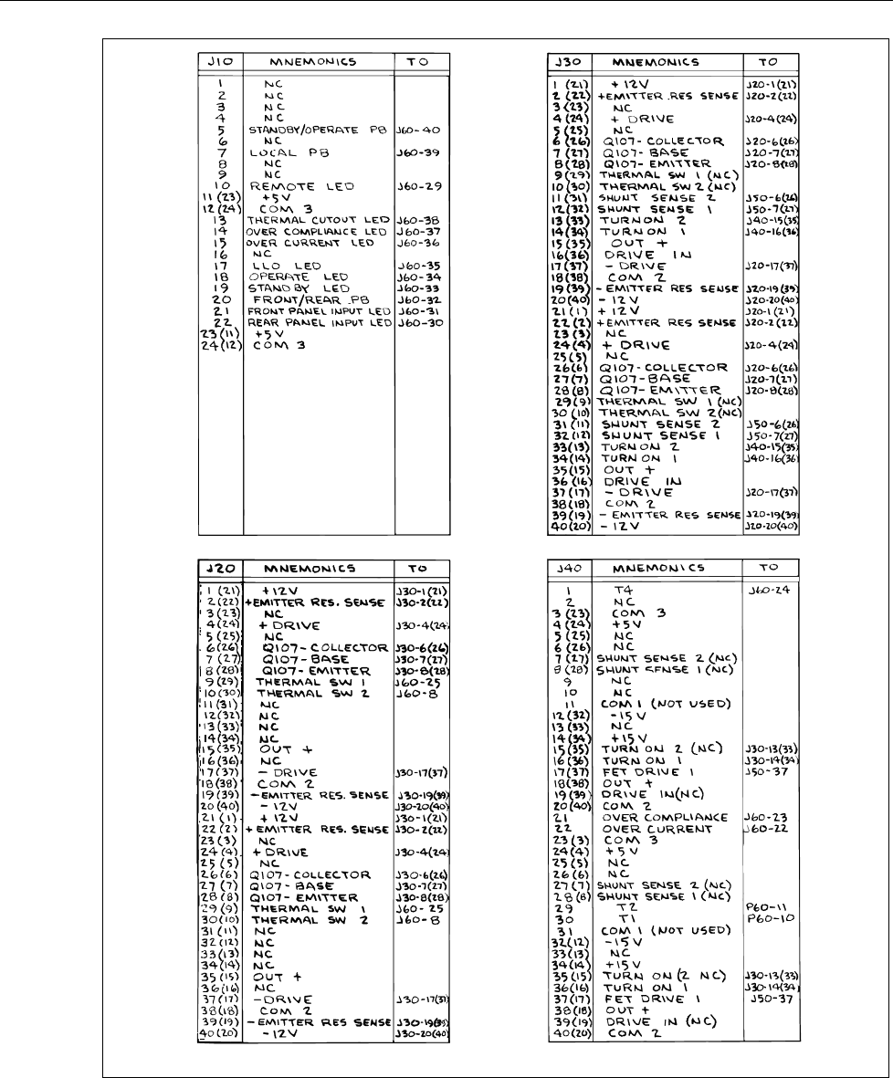
5220A
Instruction Manual
7-2
5220A-1001 (Sheet 1 of 2)
ajs47f.wmf
Figure 7-1. Interconnect Diagram
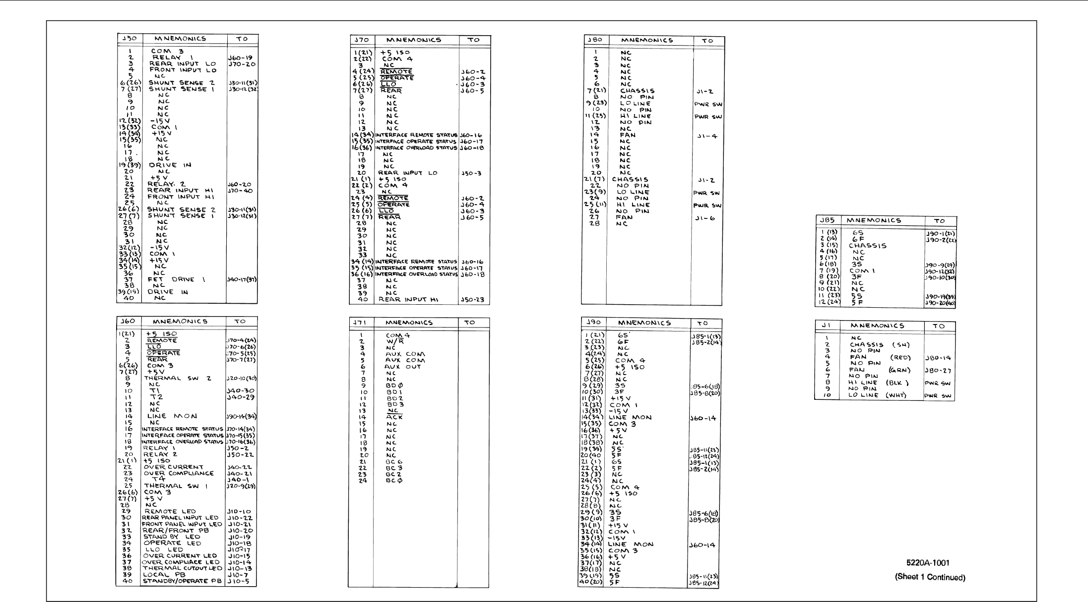
Schematic Diagrams
7
7-3
ajs48f.wm
Figure 7-1. Interconnect Diagram (cont.)
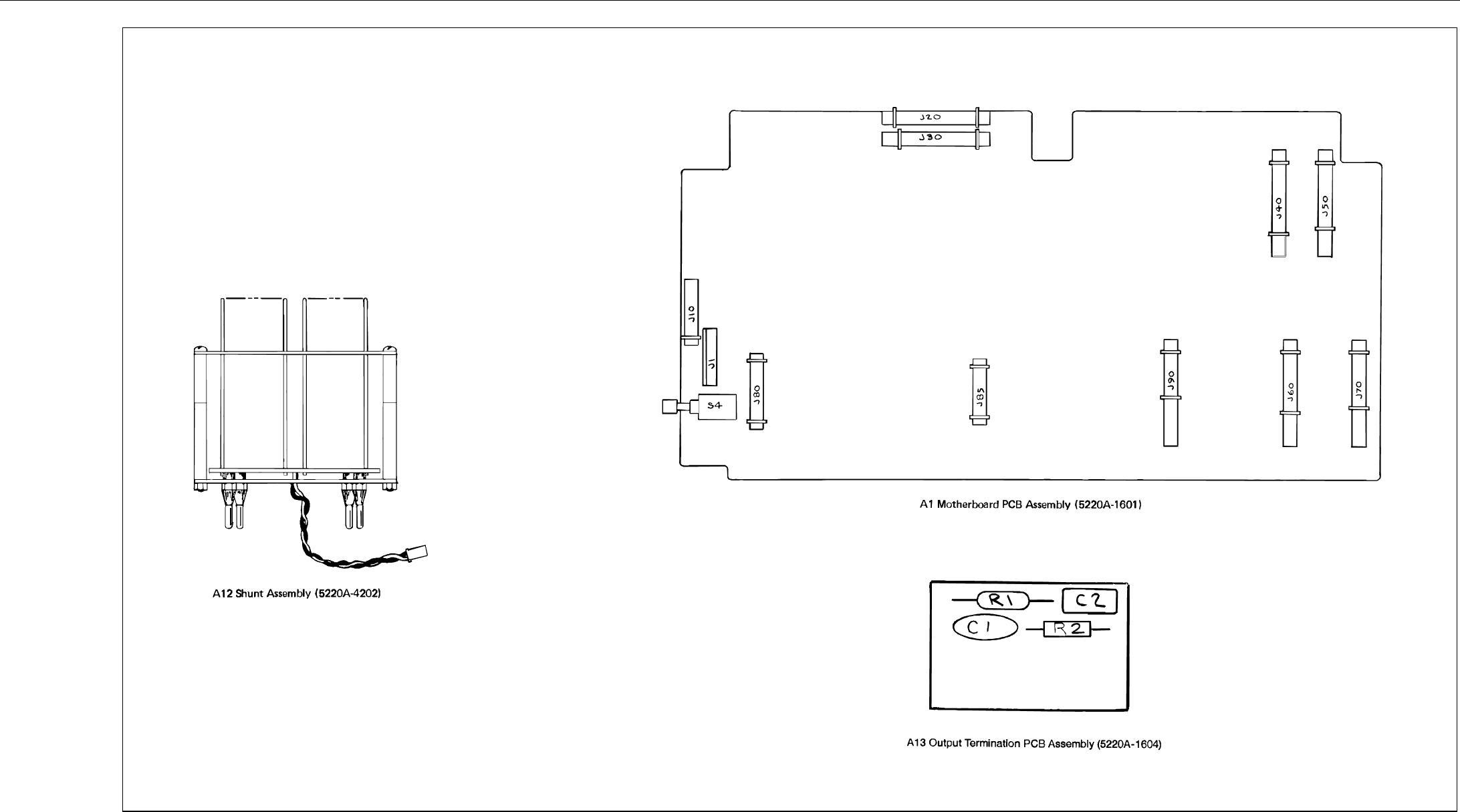
5220A
Instruction Manual
7-4
ajs49f.wmf
Figure 7-2. Chassis Wiring
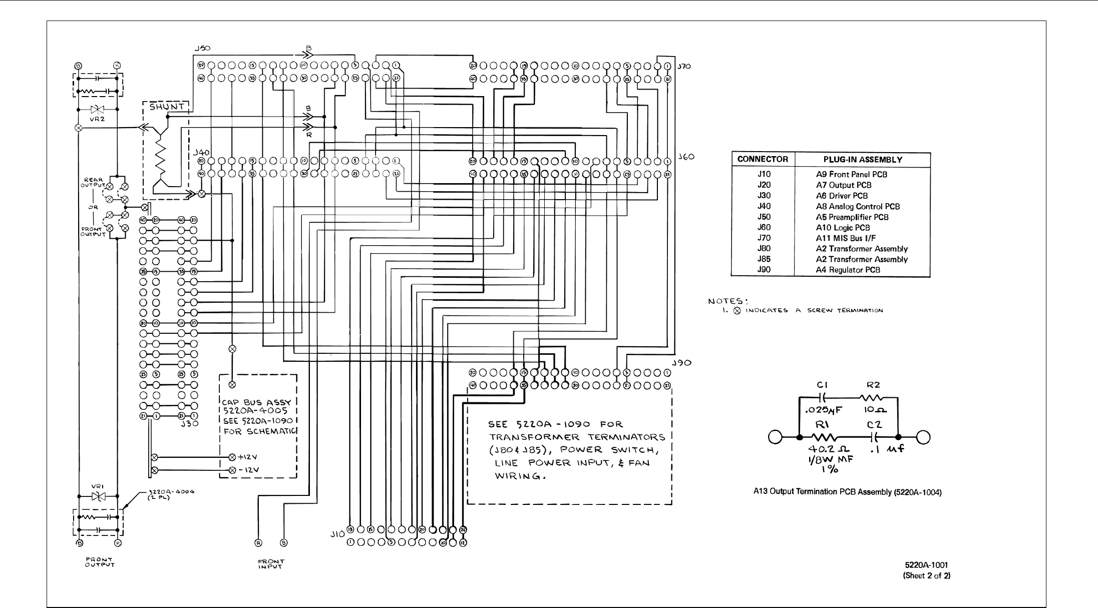
Schematic Diagrams
7
7-5
ajs50f.wmf
Figure 7-2. Chassis Wiring (cont.)
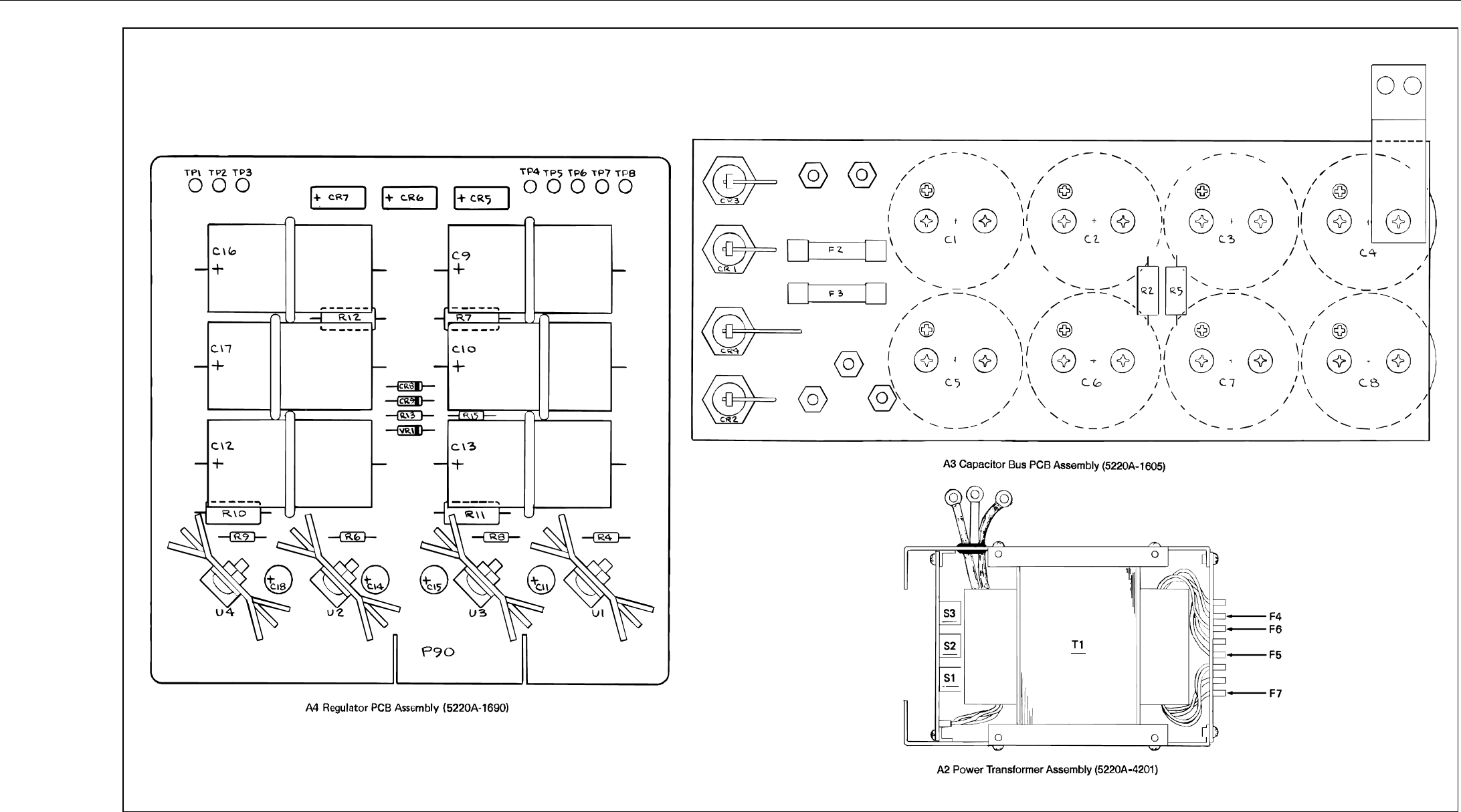
5220A
Instruction Manual
7-6
ajs51f.wmf
Figure 7-3. Power Supply
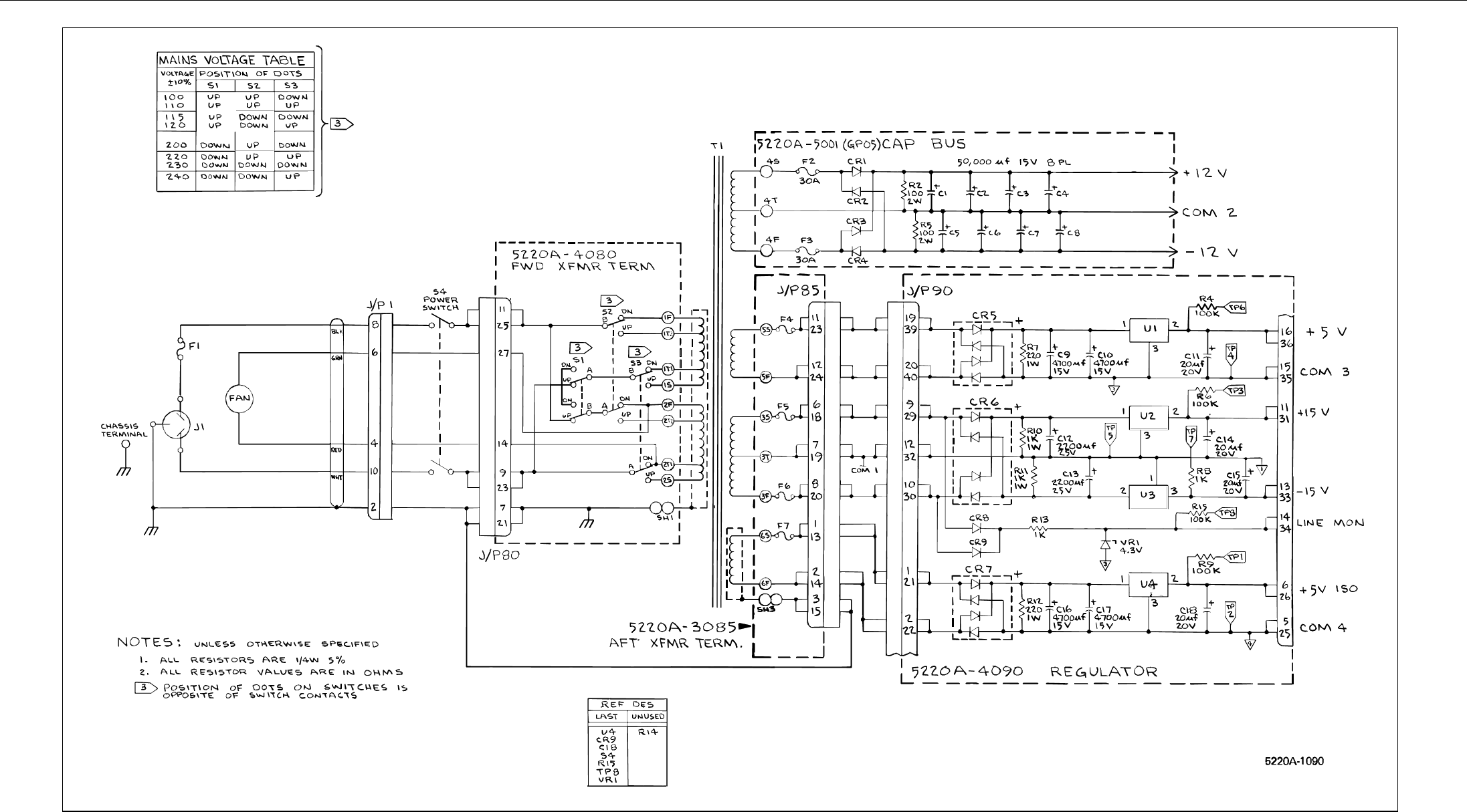
Schematic Diagrams
7
7-7
ajs52f.wmf
Figure 7-3. Power Supply (cont.)
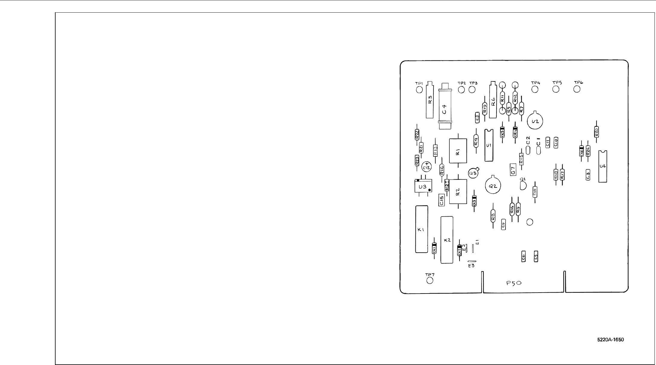
5220A
Instruction Manual
7-8
ajs53f.wmf
Figure 7-4. A5 Preamplifier PCB Assembly
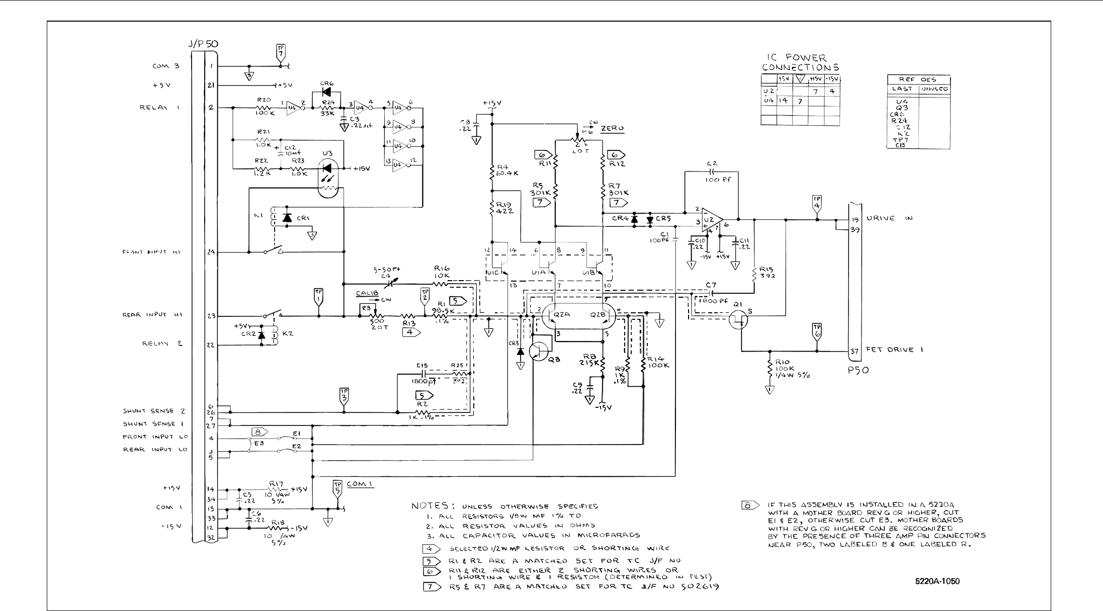
Schematic Diagrams
7
7-9
ajs54f.wmf
Figure 7-4. A5 Preamplifier PCB Assembly (cont.)
5220A
Instruction Manual
7-10
ajs55f.wmf
Figure 7-5. A6 Driver and A7 Output PCB Assemblies
Schematic Diagrams
7
7-11
ajs56f.wmf
Figure 7-5. A6 Driver and A7 Output
PCB Assemblies (cont.)
5220A
Instruction Manual
7-12
ajs57f.wmf
Figure 7-6. A8 Analog Control PCB Assembly
Schematic Diagrams
7
7-13
ajs58f.wmf
Figure 7-6. A8 Analog Control PCB Assembly (cont.)
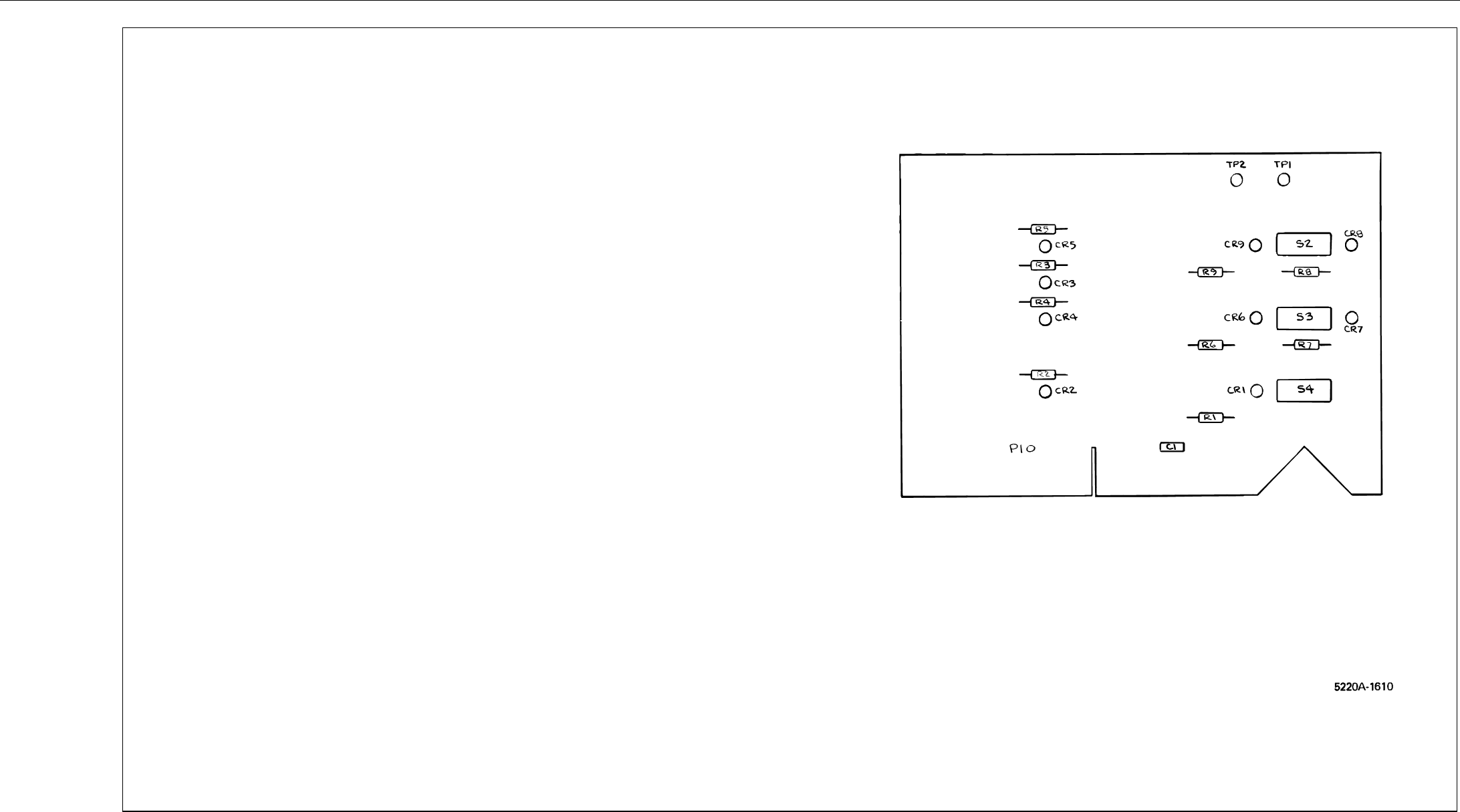
5220A
Instruction Manual
7-14
ajs59f.wmf
Figure 7-7. A9 Front Panel PCB Assembly
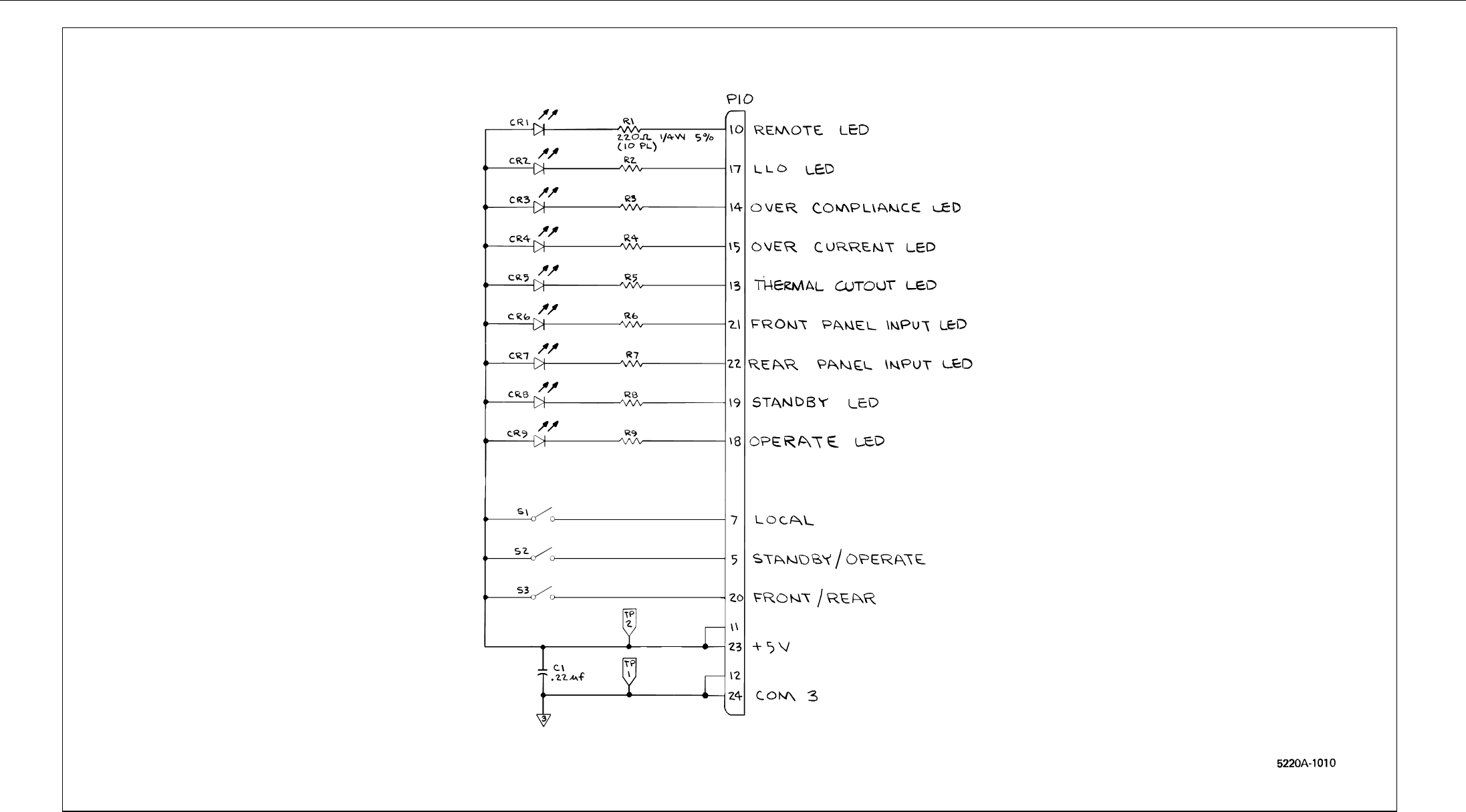
Schematic Diagrams
7
7-15
ajs60f.wmf
Figure 7-7. A9 Front Panel PCB Assembly (cont.)
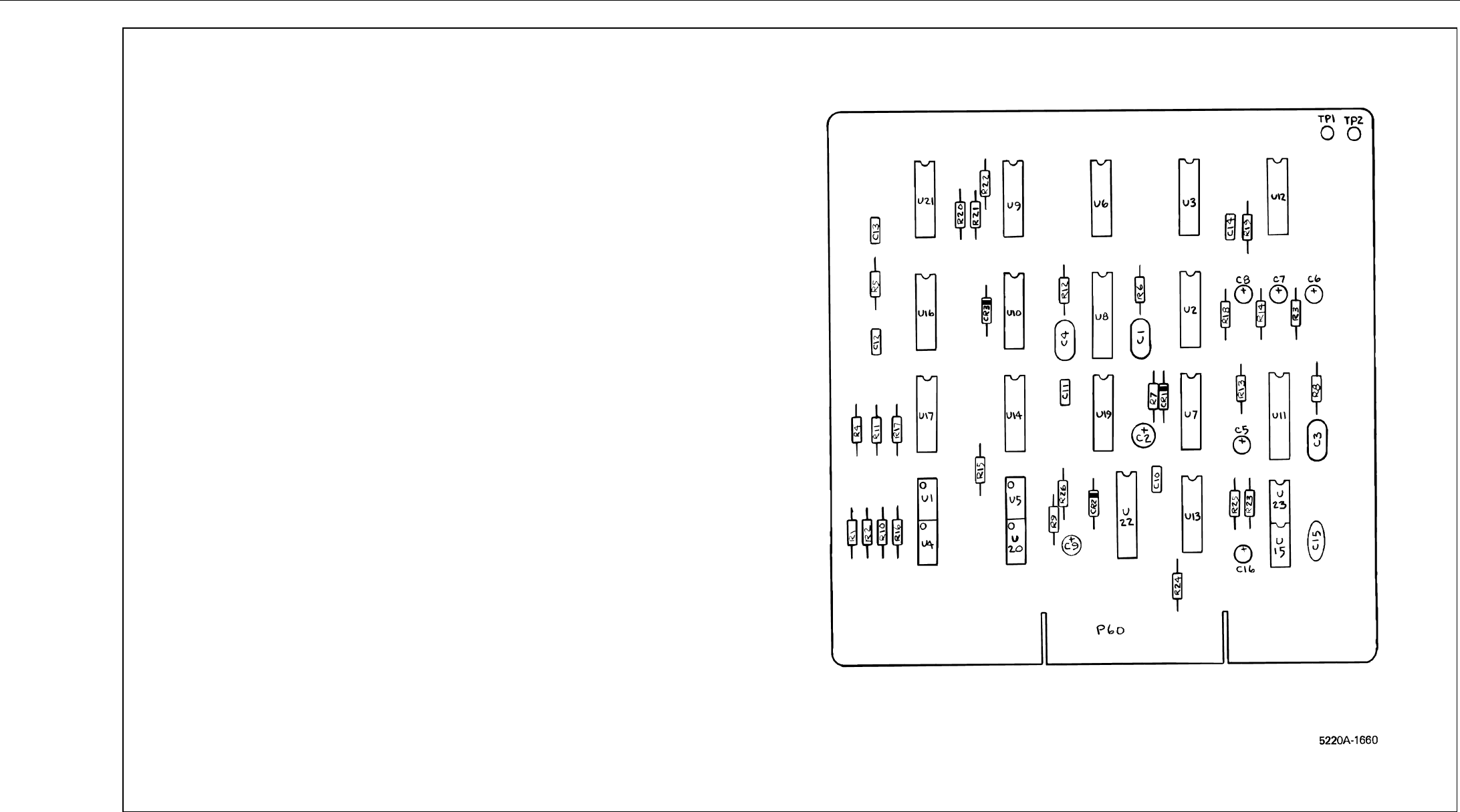
5220A
Instruction Manual
7-16
ajs61f.wmf
Figure 7-8. A10 Logic PCB Assembly
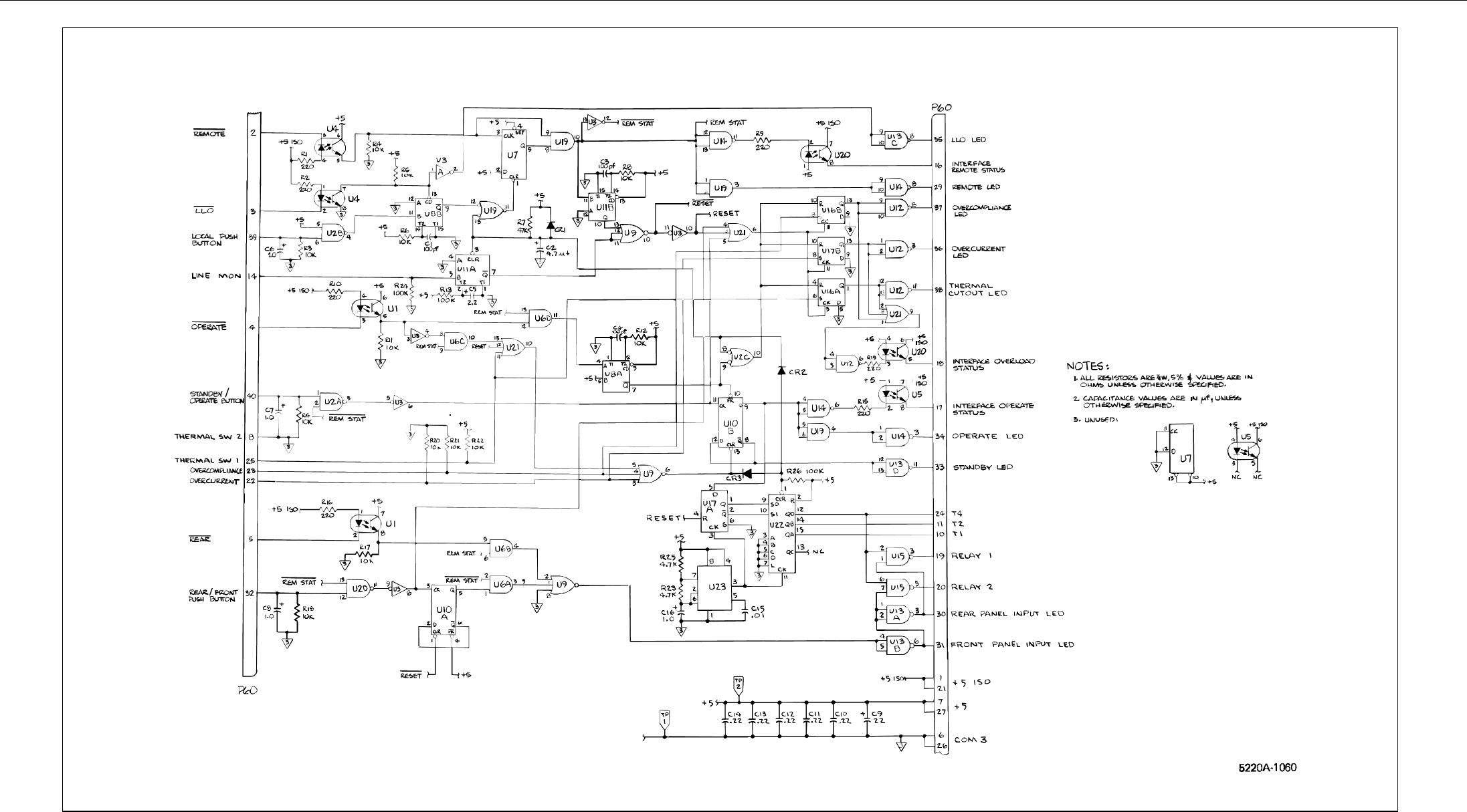
Schematic Diagrams
7
7-17
ajs62f.wmf
Figure 7-8. A10 Logic PCB Assembly (cont.)
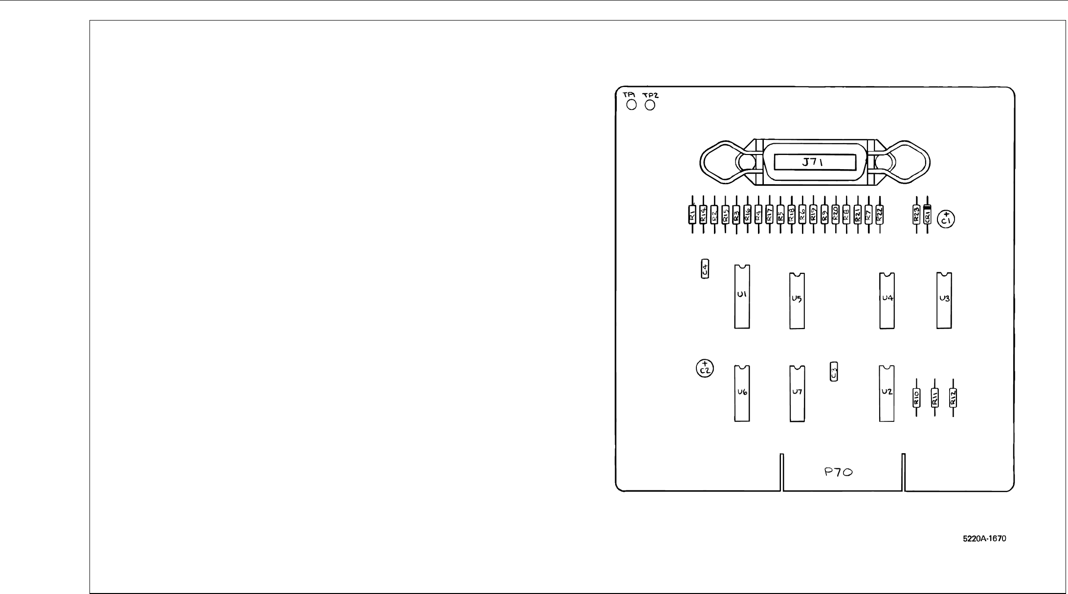
5220A
Instruction Manual
7-18
ajs63f.wmf
Figure 7-9. A11 MIS Bus Interface PCB Assembly
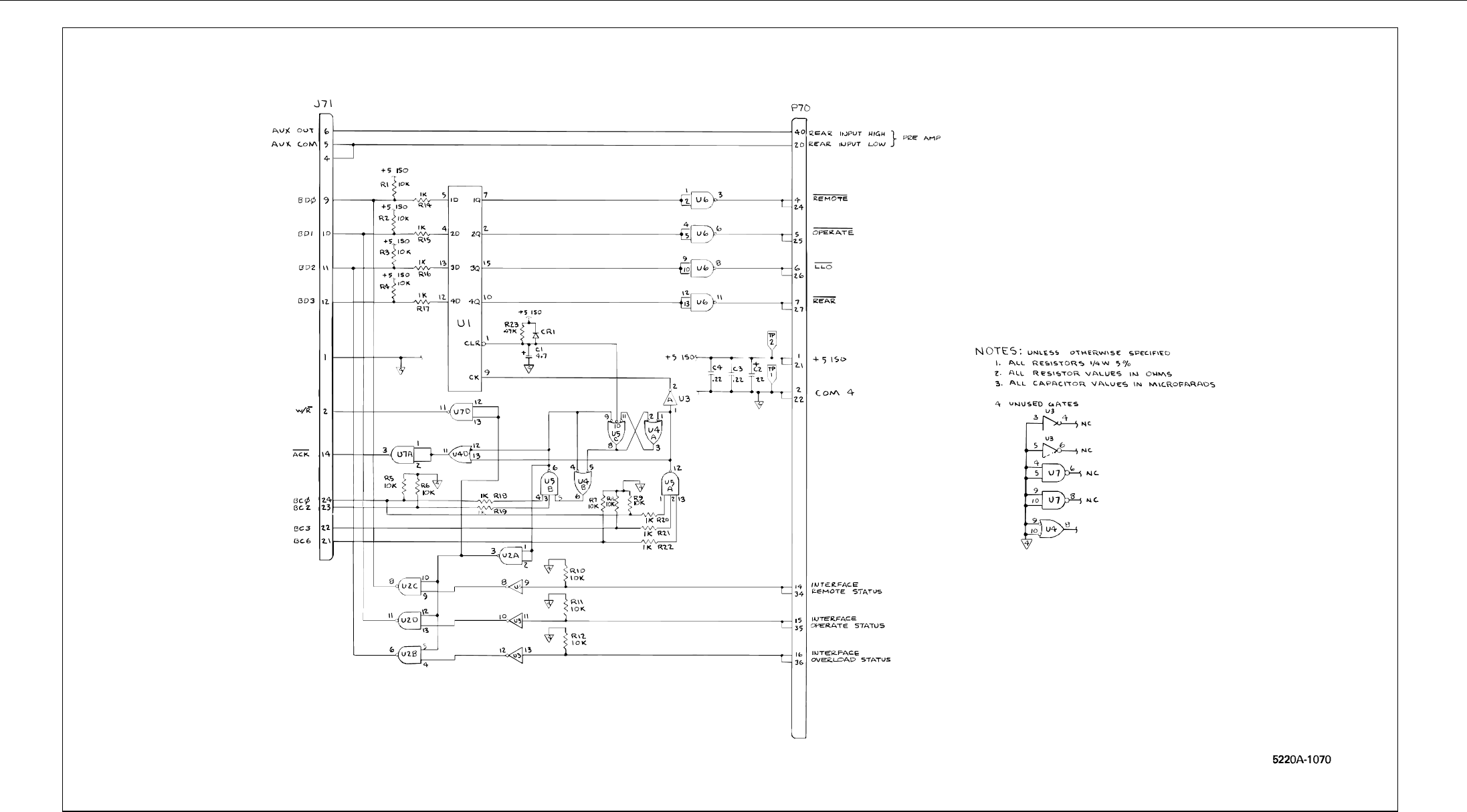
Schematic Diagrams
7
7-19
ajs64f.wmf
Figure 7-9. A11 MIS Bus Interface
PCB Assembly (cont.)

5220A
Instruction Manual
7-20
