Fluke Portable Multimedia Player 8842A Users Manual
8842a to the manual 53799805-bae4-40be-aa4a-310993d62c2c
2015-02-02
: Fluke Fluke-Fluke-Portable-Multimedia-Player-8842A-Users-Manual-427848 fluke-fluke-portable-multimedia-player-8842a-users-manual-427848 fluke pdf
Open the PDF directly: View PDF ![]() .
.
Page Count: 269 [warning: Documents this large are best viewed by clicking the View PDF Link!]
- 8842A Instruction Manual
- 1. Introduction and Specifications
- 2. Operating Instructions
- INTRODUCTION
- INSTALLATION
- OPERATING FEATURES
- MAKING MEASUREMENTS
- EXTERNAL CLEANING
- 3. Remote Programming
- INTRODUCTION
- CAPABILITIES
- BUS SET-UP PROCEDURE
- AN OVERVIEW OF REMOTE OPERATION
- A NOTE ABOUT EXAMPLES
- DEVICE-DEPENDENT COMMAND SET
- Bn (Offset Commands)
- Cn (Calibration Commands)
- Dn (Display Commands)
- Fn (Function Commands)
- Get Commands
- G0 (Get Instrument Configuration)
- G1 (Get SRQ Mask)
- G2 (Get Calibration Prompt)
- G3 (Get User-Defined Message)
- G4 (Get Calibration Status)
- G5 (Get IAB Status)
- G6 (Get YW Status)
- G7 (Get Error Status)
- G8 (Get Instrument Identification)
- N (Numeric Entry Command)
- Put Commands
- P0 (Put Instrument Configuration)
- P1 (Put SRQ Mask)
- P2 (Put Calibration Value)
- P3 (Put User-Defined Message)
- Rn (Range Commands)
- Sn (Reading Rate Commands)
- Tn (Trigger Mode Commands)
- Wn (Terminator Commands)
- X0 (Clear Error Register Command)
- Yn (Suffix Commands)
- Z0 (Self-Test Command)
- (Device-Clear Command)
- ? (Single-Trigger Command)
- INPUT SYNTAX
- OUTPUT DATA
- SERVICE REQUESTS
- INTERFACE MESSAGES
- TALK-ONLY MODE
- REMOTE CALIBRATION
- TIMING CONSIDERATIONS
- IMMEDIATE MODE COMMANDS
- EXAMPLE PROGRAMS
- 4. Measurement Tutorial
- 5. Theory of Operation
- INTRODUCTION
- OVERALL FUNCTIONAL DESCRIPTION
- DETAILED CIRCUIT DESCRIPTION
- DC SCALING
- TRACK/HOLD CIRCUIT
- PRECISION VOLTAGE REFERENCE
- OHMS CURRENT SOURCE
- OHMS PROTECTION
- OHMS FUNCTIONS
- A/D CONVERTER
- DISPLAY
- KEYBOARD
- DIGITAL CONTROLLER
- GUARD CROSSING
- POWER SUPPLY
- IEEE-488 INTERFACE (OPTION -05)
- TRUE RMS AC (OPTION -09)
- Static Awareness
- 6. Maintenance
- INTRODUCTION
- PERFORMANCE TEST
- CALIBRATION
- DISASSEMBLY PROCEDURE
- REASSEMBLY PROCEDURE
- INTERNAL FUSE REPLACEMENT
- EXTERNAL TRIGGER POLARITY SELECTION (Option -05 Only)
- TROUBLESHOOTING
- Initial Troubleshooting Procedure
- Diagnostic Self-Tests
- Self-Test Descriptions
- Digital Controller Troubleshooting
- DC Scaling Troubleshooting
- Track/Hold Troubleshooting
- Ohms Current Source Troubleshooting
- Precision Voltage Reference Troubleshooting
- A/D Converter Troubleshooting
- Power Supply Troubleshooting
- IEEE-488 Interface Troubleshooting (Option -05)
- True RMS AC Troubleshooting (Option -09)
- Guard Crossing Troubleshooting
- INTERNAL CLEANING
- Cleaning After Soldering
- 7. List of Replaceable Parts
- 8. Options and Accessories
- INTRODUCTION
- ACCESSORIES
- Rack-Mount Kits (Y8834, Y8835 and Y8836)
- Shielded IEEE-488 Interface Cables (Y8021, Y8022, and Y8023)
- Replacement Test Leads (TL70A)
- Deluxe Test Lead Kits (Y8134)
- Slim-Flex Test Leads (Y8140)
- Temperature Probes (80T-150U, and 80TK.)
- RF Probes (85RF and 83RF)
- Current Shunt (80J-10)
- Current Probes (Y8100, Y8101, 80i-400 and 80i-600)
- High Voltage Probes (80K-6 and 80K-40)
- 805. Option -05 IEEE-488 Interface
- 809. Option -09 True RMS AC
- 9. Schematic Diagrams

®
8842A
Digital Multimeter
Instruction Manual
PN 879309
Date December 1991
Rev.3 7/96
© 1999 Fluke Corporation, All rights reserved. Printed in USA
All product names are trademarks of their respective companies.
i
Table of Contents
Chapter Title Page
1 Introduction and Specifications........................................................ 1-1
1-1. INTRODUCTION................................................................................ 1-2
1-2. THE 8842A DIGITAL MULTIMETER.............................................. 1-2
1-3. OPTIONS AND ACCESSORIES........................................................ 1-2
1-4. SPECIFICATIONS .............................................................................. 1-3
2 Operating Instructions....................................................................... 2-1
2-1. INTRODUCTION................................................................................ 2-2
2-2. INSTALLATION................................................................................. 2-2
2-3. Installing the Power-Line Fuse ........................................................ 2-2
2-4. Connecting to Line Power................................................................ 2-2
2-5. Adjusting the Handle........................................................................ 2-3
2-6. Rack Mounting Kits......................................................................... 2-3
2-7. OPERATING FEATURES .................................................................. 2-4
2-8. Power-Up Features........................................................................... 2-4
2-9. Front and Rear Panel Features ......................................................... 2-4
2-10. Display Features............................................................................... 2-8
2-11. Error Messages................................................................................. 2-8
2-12. Overrange Indication........................................................................ 2-10
2-13. Diagnostic Self-Tests ....................................................................... 2-10
2-14. Ranging ............................................................................................ 2-10
2-15. AUTORANGE............................................................................. 2-10
2-16. MANUAL RANGE..................................................................... 2-11
2-17. Triggering......................................................................................... 2-11
2-18. CONTINUOUS TRIGGER MODE ............................................ 2-11
2-19. EXTERNAL TRIGGER MODE ................................................. 2-11
2-20. Reading Rates and Noise Rejection ................................................. 2-11
2-21. Automatic Settling Time Delay........................................................ 2-12
2-22. External Trigger Input (Option -05 Only)........................................ 2-12
2-23. Sample Complete Output (Option -05 Only) ................................... 2-12
2-24. MAKING MEASUREMENTS............................................................ 2-13
2-25. Input Overload Protection Limits..................................................... 2-13
2-26. Measuring Voltage and Resistance .................................................. 2-13
2-27. Measuring Current ........................................................................... 2-13

8842A
Instruction Manual
ii
2-28. Current Fuse Protection.................................................................... 2-13
2-29. Offset Measurements ....................................................................... 2-14
2-30. EXTERNAL CLEANING.................................................................... 2-15
3 Remote Programming........................................................................ 3-1
3-1. INTRODUCTION................................................................................ 3-3
3-2. CAPABILITIES ................................................................................... 3-3
3-3. BUS SET-UP PROCEDURE............................................................... 3-3
3-4. AN OVERVIEW OF REMOTE OPERATION................................... 3-4
3-5. A NOTE ABOUT EXAMPLES........................................................... 3-6
3-6. DEVICE-DEPENDENT COMMAND SET ........................................ 3-6
3-7. Bn (Offset Commands) .................................................................... 3-9
3-8. Cn (Calibration Commands) ............................................................ 3-9
3-9. Dn (Display Commands).................................................................. 3-9
3-10. Fn (Function Commands) ................................................................ 3-10
3-11. Get Commands................................................................................. 3-10
3-12. G0 (Get Instrument Configuration).................................................. 3-12
3-13. G1 (Get SRQ Mask)......................................................................... 3-12
3-14. G2 (Get Calibration Prompt)............................................................ 3-12
3-15. G3 (Get User-Defined Message)...................................................... 3-13
3-16. G4 (Get Calibration Status).............................................................. 3-13
3-17. G5 (Get IAB Status)......................................................................... 3-14
3-18. G6 (Get YW Status)......................................................................... 3-14
3-19. G7 (Get Error Status) ....................................................................... 3-14
3-20. G8 (Get Instrument Identification)................................................... 3-14
3-21. N (Numeric Entry Command).......................................................... 3-15
3-22. Put Commands ................................................................................. 3-15
3-23. P0 (Put Instrument Configuration)................................................... 3-15
3-24. P1 (Put SRQ Mask).......................................................................... 3-16
3-25. P2 (Put Calibration Value).............................................................. 3-16
3-26. P3 (Put User-Defined Message)...................................................... 3-17
3-27. Rn (Range Commands).................................................................... 3-17
3-28. Sn (Reading Rate Commands)......................................................... 3-17
3-29. Tn (Trigger Mode Commands) ........................................................ 3-17
3-30. Wn (Terminator Commands) ........................................................... 3-19
3-31. X0 (Clear Error Register Command) ............................................... 3-19
3-32. Yn (Suffix Commands).................................................................... 3-19
3-33. Z0 (Self-Test Command) ................................................................. 3-19
3-34. (Device-Clear Command)................................................................ 3-20
3-35. ? (Single-Trigger Command) ........................................................... 3-20
3-36. INPUT SYNTAX................................................................................. 3-20
3-37. Definitions........................................................................................ 3-20
3-38. Input Processing............................................................................... 3-21
3-39. Syntax Rules .................................................................................... 3-23
3-40. OUTPUT DATA .................................................................................. 3-24
3-41. Loading Output Data........................................................................ 3-24
3-42. Types of Output Data....................................................................... 3-25
3-43. Numeric Data and Error Messages................................................... 3-25
3-44. MEASUREMENT DATA........................................................... 3-25
3-45. OVERRANGE INDICATION .................................................... 3-26
3-46. ERROR MESSAGES .................................................................. 3-26
3-47. Status Data ....................................................................................... 3-26
3-48. Output Priority ................................................................................. 3-26
3-49. SERVICE REQUESTS ........................................................................ 3-27

Contents
(continued)
iii
3-50. The Serial Poll Register ................................................................... 3-27
3-51. The SRQ Mask................................................................................. 3-28
3-52. INTERFACE MESSAGES .................................................................. 3-29
3-53. Address Messages............................................................................ 3-29
3-54. Universal Commands....................................................................... 3-29
3-55. Addressed Commands...................................................................... 3-30
3-56. TALK-ONLY MODE .......................................................................... 3-30
3-57. REMOTE CALIBRATION.................................................................. 3-31
3-58. TIMING CONSIDERATIONS............................................................ 3-31
3-59. IMMEDIATE MODE COMMANDS.................................................. 3-31
3-60. EXAMPLE PROGRAMS .................................................................... 3-32
4 Measurement Tutorial........................................................................ 4-1
4-1. INTRODUCTION................................................................................ 4-2
4-2. DC VOLTAGE MEASUREMENT ..................................................... 4-2
4-3. Circuit Loading Error....................................................................... 4-2
4-4. Input Bias Current Error................................................................... 4-3
4-5. RESISTANCE MEASUREMENT ...................................................... 4-4
4-6. 2-Wire Ohms.................................................................................... 4-4
4-7. Correcting for Test Lead Resistance in 2-Wire Ohms ..................... 4-5
4-8. 4-Wire Ohms.................................................................................... 4-5
4-9. Applications of the Ohms Functions................................................ 4-7
4-10. TESTING DIODES..................................................................... 4-7
4-11. TESTING ELECTROLYTIC CAPACITORS ............................ 4-7
4-12. A PRECISION CURRENT SOURCE......................................... 4-8
4-13. DC CURRENT MEASUREMENT ..................................................... 4-8
4-14. REDUCING THERMAL VOLTAGES............................................... 4-9
4-15. AC VOLTAGE AND CURRENT MEASUREMENT........................ 4-10
4-16. True RMS Measurement.................................................................. 4-10
4-17. Waveform Comparison.................................................................... 4-10
4-18. Crest Factor...................................................................................... 4-12
4-19. AC-Coupled AC Measurements ...................................................... 4-12
4-20. Combined AC and DC Measurements............................................. 4-13
4-21. Bandwidth ........................................................................................ 4-13
4-22. Zero-Input VAC Error...................................................................... 4-13
4-23. MAKING ACCURATE MEASUREMENTS ON THE 20 mV
AND 20Ω RANGES ............................................................................ 4-14
4-24. MAKING ACCURATE HIGH-RESISTANCE MEASUREMENTS . 4-15
5 Theory of Operation........................................................................... 5-1
5-1. INTRODUCTION................................................................................ 5-3
5-2. OVERALL FUNCTIONAL DESCRIPTION...................................... 5-3
5-3. DETAILED CIRCUIT DESCRIPTION .............................................. 5-4
5-4. DC SCALING ...................................................................................... 5-4
5-5. VDC Scaling .................................................................................... 5-6
5-6. VDC Protection................................................................................ 5-7
5-7. mA DC Scaling................................................................................ 5-7
5-8. Analog Filter .................................................................................... 5-7
5-9. TRACK/HOLD CIRCUIT ................................................................... 5-8
5-10. Track Configuration......................................................................... 5-10
5-11. Settling Configuration...................................................................... 5-11
5-12. Hold Configuration .......................................................................... 5-11
5-13. Pre-Charge Configuration................................................................ 5-11
5-14. PRECISION VOLTAGE REFERENCE.............................................. 5-11

8842A
Instruction Manual
iv
5-15. OHMS CURRENT SOURCE .............................................................. 5-12
5-16. OHMS PROTECTION......................................................................... 5-13
5-17. OHMS FUNCTIONS ........................................................................... 5-13
5-18. 2-Wire Ohms.................................................................................... 5-13
5-19. 4-Wire Ohms.................................................................................... 5-15
5-20. A/D CONVERTER .............................................................................. 5-15
5-21. Timing/Data Control........................................................................ 5-17
5-22. Precision DAC ................................................................................. 5-18
5-23. A/D Amplifier.................................................................................. 5-18
5-24. Bootstrap Supplies ........................................................................... 5-18
5-25. DISPLAY ............................................................................................. 5-19
5-26. KEYBOARD........................................................................................ 5-19
5-27. DIGITAL CONTROLLER................................................................... 5-19
5-28. In-Guard Microcomputer ................................................................. 5-21
5-29. Function and Range Control ............................................................ 5-23
5-30. A/D Control and Computation......................................................... 5-23
5-31. Calibration Correction...................................................................... 5-23
5-32. Keyboard/Display Control ............................................................... 5-24
5-33. Troubleshooting Modes ................................................................... 5-24
5-34. Guard-Crossing Communication ..................................................... 5-24
5-35. GUARD CROSSING ........................................................................... 5-24
5-36. POWER SUPPLY ................................................................................ 5-25
5-37. IEEE-488 INTERFACE (OPTION -05)............................................... 5-26
5-38. Out-Guard Microcomputer............................................................... 5-26
5-39. Guard Crossing................................................................................. 5-26
5-40. Bus Interface Circuitry..................................................................... 5-26
5-41. Signal Conditioning ......................................................................... 5-27
5-42. IEEE-488 Interface Power Supply................................................... 5-27
5-43. TRUE RMS AC (OPTION -09) ........................................................... 5-27
5-44. VAC Scaling .................................................................................... 5-27
5-45. mA AC Scaling................................................................................ 5-28
5-46. Frequency Response Trimming ....................................................... 5-28
5-47. True RMS AC-to-DC Conversion ................................................... 5-28
6 Maintenance ....................................................................................... 6-1
6-1. INTRODUCTION................................................................................ 6-3
6-2. PERFORMANCE TEST...................................................................... 6-4
6-3. Diagnostic Self-Tests ....................................................................... 6-4
6-4. DC Voltage Test............................................................................... 6-5
6-5. AC Voltage Test (Option -09 Only)................................................. 6-7
6-6. Resistance Test................................................................................. 6-8
6-7. DC Current Test............................................................................... 6-9
6-8. AC Current Test (Option -09 Only)................................................. 6-10
6-9. CALIBRATION................................................................................... 6-10
6-10. Basic Calibration Procedure............................................................. 6-11
6-11. INITIAL PROCEDURE.............................................................. 6-11
6-12. A/D CALIBRATION .................................................................. 6-12
6-13. OFFSET AND GAIN CALIBRATION ...................................... 6-14
6-14. HIGH-FREQUENCY AC CALIBRATION................................ 6-15
6-15. Advanced Features and Special Considerations............................... 6-16
6-16. STORING VARIABLE INPUTS................................................ 6-16
6-17. CALIBRATING INDIVIDUAL RANGES................................. 6-17
6-18. VERIFYING CALIBRATION.................................................... 6-17
6-19. ERASING CALIBRATION MEMORY..................................... 6-18

Contents
(continued)
v
6-20. TOLERANCE CHECK ............................................................... 6-18
6-21. AC CALIBRATION AT OTHER FREQUENCIES ................... 6-19
6-22. OPTIMIZING USE OF THE 5450A........................................... 6-19
6-23. Remote Calibration .......................................................................... 6-20
6-24. TIMING CONSIDERATIONS ................................................... 6-23
6-25. REMOTE ERASURE.................................................................. 6-24
6-26. EXAMPLE CALIBRATION PROGRAM.................................. 6-24
6-27. DISASSEMBLY PROCEDURE.......................................................... 6-25
6-28. Case Removal................................................................................... 6-26
6-29. True RMS AC PCA Removal (Option -09 Only)............................ 6-30
6-30. IEEE-488 Interface PCA Removal (Option -05 Only) .................... 6-30
6-31. Main PCA Removal......................................................................... 6-30
6-32. Front Panel Disassembly.................................................................. 6-32
6-33. REASSEMBLY PROCEDURE........................................................... 6-32
6-34. INTERNAL FUSE REPLACEMENT ................................................. 6-36
6-35. EXTERNAL TRIGGER POLARITY SELECTION (Option -05 Only)6-36
6-36. TROUBLESHOOTING ....................................................................... 6-36
6-37. Initial Troubleshooting Procedure.................................................... 6-36
6-38. Diagnostic Self-Tests ....................................................................... 6-41
6-39. Self-Test Descriptions...................................................................... 6-42
6-40. Digital Controller Troubleshooting.................................................. 6-45
6-41. IN-GUARD MICROCOMPUTER SYSTEM............................. 6-45
6-48. DISPLAY SYSTEM.................................................................... 6-49
6-59. ANALOG CONTROL SIGNALS............................................... 6-51
6-62. DC Scaling Troubleshooting............................................................ 6-54
6-63. Track/Hold Troubleshooting............................................................ 6-56
6-64. Ohms Current Source Troubleshooting............................................ 6-56
6-65. Precision Voltage Reference Troubleshooting................................. 6-58
6-66. A/D Converter Troubleshooting....................................................... 6-59
6-67. Power Supply Troubleshooting........................................................ 6-61
6-68. IEEE-488 Interface Troubleshooting (Option -05) .......................... 6-64
6-69. SERVICE POSITION.................................................................. 6-64
6-70. DIAGNOSTIC PROGRAM ........................................................ 6-64
6-71. True RMS AC Troubleshooting (Option -09).................................. 6-66
6-72. SERVICE POSITION.................................................................. 6-66
6-73. MAJOR PROBLEMS.................................................................. 6-67
6-74. MORE OBSCURE PROBLEMS ................................................ 6-69
6-75. Guard Crossing Troubleshooting..................................................... 6-70
6-76. INTERNAL CLEANING..................................................................... 6-70
6-77. Cleaning Printed Circuit Assemblies ............................................... 6-70
6-78. Cleaning After Soldering ................................................................. 6-71
7 List of Replaceable Parts................................................................... 7-1
7-1. INTRODUCTION................................................................................ 7-3
7-2. HOW TO OBTAIN PARTS................................................................. 7-3
7-3. MANUAL STATUS INFORMATION................................................ 7-3
7-4. NEWER INSTRUMENTS................................................................... 7-4
7-5. SERVICE CENTERS........................................................................... 7-4
8 Options and Accessories.................................................................. 8-1
8-1. INTRODUCTION................................................................................ 8-3
8-2. ACCESSORIES ................................................................................... 8-4
8-3. Rack-Mount Kits (Y8834, Y8835 and Y8836)................................ 8-4
8-4. Shielded IEEE-488 Interface Cables (Y8021, Y8022, and Y8023). 8-4

8842A
Instruction Manual
vi
8-5. Replacement Test Leads (TL70A)................................................... 8-4
8-6. Deluxe Test Lead Kits (Y8134) ....................................................... 8-4
8-7. Slim-Flex Test Leads (Y8140)......................................................... 8-4
8-8. Temperature Probes (80T-150U, and 80TK.).................................. 8-4
8-9. RF Probes (85RF and 83RF)............................................................ 8-4
8-10. Current Shunt (80J-10)..................................................................... 8-5
8-11. Current Probes (Y8100, Y8101, 80i-400 and 80i-600).................... 8-5
8-12. High Voltage Probes (80K-6 and 80K-40) ...................................... 8-5
805 Option –05 IEEE-488 Interface........................................................... 805-1
805-1. INTRODUCTION................................................................................ 805-3
805-2. CAPABILITIES ................................................................................... 805-3
805-3. EXTERNAL CONTROLS................................................................... 805-3
805-4. INSTALLATION................................................................................. 805-3
805-5. PROGRAMMING INSTRUCTIONS.................................................. 805-4
805-6. MAINTENANCE................................................................................. 805-4
805-7. LIST OF REPLACEABLE PARTS..................................................... 805-4
809 Option –09 True RMS AC................................................................... 809-1
809-1. INTRODUCTION................................................................................ 809-3
809-2. INSTALLATION................................................................................. 809-3
809-3. OPERATING INSTRUCTIONS.......................................................... 809-4
809-4. MAINTENANCE................................................................................. 809-4
809-5. LIST OF REPLACEABLE PARTS..................................................... 809-4
9 Schematic Diagrams.......................................................................... 9-1
vii
List of Tables
Table Title Page
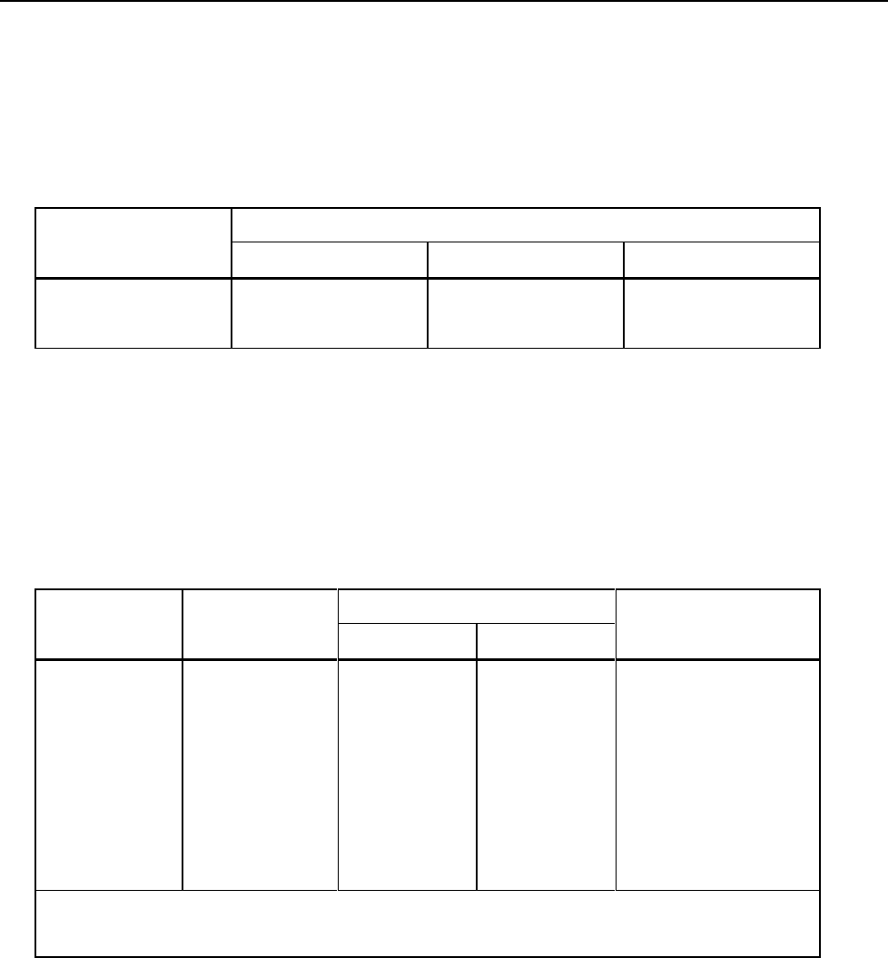
2-1. Error Codes............................................................................................................ 2-9
2-2. Input Overload Limits............................................................................................ 2-13
3-1. Status Data............................................................................................................. 3-11
3-2. Numeric Output Data Format ................................................................................ 3-25
3-8. Serial Poll Register ................................................................................................ 3-28
3-3. Immediate-Mode Commands for Various Controllers .......................................... 3-32
3-4. ASCII/IEEE Std 488-1978 Bus Codes .................................................................. 3-49
4-1. Ohms Test Current................................................................................................. 4-6
5-1. Sample Rates and Reading Rates........................................................................... 5-23
6-1. Recommended Test Equipment ............................................................................. 6-3
6-2. DC Voltage Test .................................................................................................... 6-6
6-3. Low- and Mid-Frequency AC Voltage Test .......................................................... 6-7
6-4. High-Frequency AC Voltage Test ......................................................................... 6-8
6-5. Resistance Test ...................................................................................................... 6-9
6-6. DC Current Test..................................................................................................... 6-9
6-7. AC Current Test..................................................................................................... 6-10
6-8. A/D Calibration Steps............................................................................................ 6-13
6-9. A/D Calibration Verification Test ......................................................................... 6-13
6-10. Offset and Gain Calibration Steps ......................................................................... 6-14
6-11. High-Frequency AC Calibration Steps .................................................................. 6-16
6-12. Prompts When Calibrating Individual Ranges....................................................... 6-17
6-13. Tolerance Limits.................................................................................................... 6-19
6-14. Commands Used During remote Calibration......................................................... 6-21
6-15. Error Numbers Which Are Displayed When Commands Are Not Valid.............. 6-23
6-16. Overall State Table ................................................................................................ 6-38
6-17. Circuitry Tested by the Analog Self-Tests............................................................. 6-40
6-18. Self-Test Voltages.................................................................................................. 6-42
6-19. Keyboard Wiring ................................................................................................... 6-51
6-20. Analog Control Devices......................................................................................... 6-52
6-21. Analog Control Logic States.................................................................................. 6-53
6-22. DC Scaling and Track/Hold Supply Voltages ....................................................... 6-55
6-23. Power Supply Voltages.......................................................................................... 6-63
6-24. Diagnostic Modes .................................................................................................. 6-65
6-25. I/O Port Configurations ......................................................................................... 6-66
6-26. Isolating a Defective AC Stage.............................................................................. 6-67

8842A
Instruction Manual
viii
6-27. AC Signal Tracing ................................................................................................. 6-68
6-28. Truth Table for U804 and K2 ................................................................................ 6-69
7-1. 8842A Digital Multimeter...................................................................................... 7-5
7-2. A1 Main PCA ........................................................................................................ 7-10
7-3. A2 Display PCA .................................................................................................... 7-14
8-1. Accessories ............................................................................................................ 8-3
8-2. Options................................................................................................................... 8-3
805-1.Option -05A IEEE-488 Interface PCA .................................................................. 805-7
809-1.Option -09 True RMS AC PCA............................................................................. 809-6
ix
List of Figures
Figure Title Page
1-1. External Dimensions.............................................................................................. 1-11
2-1. Line Voltage Selection Settings............................................................................. 2-2
2-2. Adjusting the Handle ............................................................................................. 2-3
2-3. Rack-Mount Kits.................................................................................................... 2-3
2-4. Installing the Single Rack Mount Kit .................................................................... 2-4
2-5. Front Panel Features .............................................................................................. 2-5
2-6. Rear Panel Features ............................................................................................... 2-7
2-7. Typical Error Messages ......................................................................................... 2-8
2-8. Overrange Indication ............................................................................................. 2-12
2-9. Measuring Voltage and Resistance........................................................................ 2-15
2-10. Measuring Current ................................................................................................. 2-15
3-1. IEEE-488 Address Selection.................................................................................. 3-4
3-2. Remote Operation Block Diagram......................................................................... 3-5
3-3. Typical Command String....................................................................................... 3-6
3-4. Commands Which Correspond to the Front Panel................................................. 3-7
3-5. Device-Dependent Command Set.......................................................................... 3-8
3-6. Output Data Format ............................................................................................... 3-10
3-6. Trigger Selection Logic Diagram .......................................................................... 3-18
3-7. Interpretation of Messages..................................................................................... 3-22
3-9. Example Program................................................................................................... 3-33
3-10. Example Program: Taking Readings with Local Control...................................... 3-34
3-11. Example Program: Using the Serial Poll Register................................................. 3-35
3-12. Example Program: Record Errors During Selftest................................................. 3-36
3-13. Example Programs: Using the IBM PC................................................................. 3-37
4-1. Circuit Loading Error Calculation ......................................................................... 4-2
4-2. Measuring Input Bias Current Error ...................................................................... 4-3
4-3. Wire Ohms Measurement...................................................................................... 4-4
4-4. Wire Ohms Measurement...................................................................................... 4-6
4-5. Burden Voltage Error Calculation ......................................................................... 4-9
4-6. Waveform Comparison Chart................................................................................ 4-11
4-7. Typical Crest Factors for Various Waveforms ...................................................... 4-12
4-8. Combined AC and DC Measurement .................................................................... 4-13
4-9. Reduction of Zero-Input Error............................................................................... 4-14
4-10. Shielding for Low Voltage Measurements ............................................................ 4-15
4-11. Shielding for Low Resistance Measurements........................................................ 4-15

8842A
Instruction Manual
x
4-12. Leakage Resistance in High Resistance Measurement.......................................... 4-16
5-1. Overall Functional Block Diagram........................................................................ 5-5
5-2. DC Scaling (VDC and mA DC)............................................................................. 5-6
5-3. Track/Hold Amplifier ............................................................................................ 5-8
5-4. Track/Hold Circuit Configurations........................................................................ 5-9
5-5. Timing Diagram for One A/D Cycle ..................................................................... 5-10
5-6. Precision Voltage Reference.................................................................................. 5-11
5-7. Ohms Current Source............................................................................................. 5-12
5-8. Ohms Scaling......................................................................................................... 5-14
5-9. Analog-to-Digital Converter.................................................................................. 5-16
5-10. First Remainder-Store Period ................................................................................ 5-17
5-11. Autozero Period..................................................................................................... 5-18
5-12. Vacuum Fluorescent Display................................................................................. 5-19
5-13. Digital Controller Block Diagram.......................................................................... 5-20
5-14. Read/Write Timing Diagrams for Internal Bus...................................................... 5-22
5-15. Guard Crossing Circuit.......................................................................................... 5-24
5-16. IEEE-488 Interface Block Diagram....................................................................... 5-26
5-17. True RMS AC Option Block Diagram .................................................................. 5-27
5-18. True RMS AC-to-DC Converter............................................................................ 5-28
6-1. DC Calibration Connections.................................................................................. 6-6
6-2. First A/D Calibration Prompt................................................................................. 6-11
6-3. Calibration Functions............................................................................................. 6-12
6-4. Optimizing Use of the 5450A................................................................................ 6-20
6-5. Example A/D Calibration Program........................................................................ 6-25
6-6. 8842A Disassembly ............................................................................................... 6-26
6-7. Front Panel Disassembly........................................................................................ 6-34
6-8. Removing the Display Window............................................................................. 6-35
6-9. U202 Pin Diagram ................................................................................................. 6-46
6-10. Waveforms for In-Guard Troubleshooting Mode.................................................. 6-47
6-11. Waveforms for Display Logic ............................................................................... 6-49
6-12. Typical Dynamic Control Signals.......................................................................... 6-54
6-13. Typical Output Waveforms for Track/Hold Circuit (TP103) ................................ 6-57
6-14. Output of A/D Amplifier (TP101)......................................................................... 6-59
6-15. Waveforms at U101-24 and U101-25.................................................................... 6-60
6-16. Typical Bus Data Line Waveform......................................................................... 6-60
6-17. Waveforms at TP102 for Several Inputs on 2V DV Range................................... 6-62
6-18. Calculating the A/D Reading From TP102 Waveform.......................................... 6-63
6-19. Option -05 Service Position................................................................................... 6-65
6-20. Option -09 Service Position................................................................................... 6-68
6-21. Guard Crossing Test Waveforms........................................................................... 6-71
7-1. 8842A Digital Multimeter...................................................................................... 7-6
7-2. A1 Main PCA ........................................................................................................ 7-13
7-3. A2 Display PCA .................................................................................................... 7-15
7-4. Service Centers ...................................................................................................... 7-18
7-4. Service Centers (cont)............................................................................................ 7-19
805-1.Installing Option -05.............................................................................................. 805-5
805-2.IEEE-488 Interface PCA........................................................................................ 805-8
809-1.Installing Option -09.............................................................................................. 809-5
809-2.True RMS AC PCA ............................................................................................... 809-7
9-1. Main PCA, DC Scaling and F/R Switch................................................................ 9-3
9-2. Main PCA, A/D Converter .................................................................................... 9-5
9-3. Main PCA, Ohms Current Source ......................................................................... 9-7
9-4. Main PCA, Digital ................................................................................................. 9-9
9-5. Main PCA, Power Supply...................................................................................... 9-11
9-6. Display PCA .......................................................................................................... 9-13


8842A
Instruction Manual
xii
1-1
Chapter 1
Introduction and Specifications
Title Page
1-1. INTRODUCTION................................................................................1-2
1-2. THE 8842A DIGITAL MULTIMETER..............................................1-2
1-3. OPTIONS AND ACCESSORIES........................................................1-2
1-4. SPECIFICATIONS ..............................................................................1-3

8842A
Instruction Manual
1-2
1-1. INTRODUCTION
This manual provides complete operating instructions and service information for the
8842A. If you want to get started using your 8842A right away, proceed to the operating
instructions in Section 2. If you intend to use the 8842A with the IEEE-488 Interface
(Option -05), read Sections 2 and 3. This meter has been designed and tested according to
IEC publication 348, Safety Requirements for Electronic Measuring Apparatus. This
manual contains information and warnings which must be followed to ensure safe
operation and retain the meter in safe condition.
1-2. THE 8842A DIGITAL MULTIMETER
The Fluke 8842A Digital Multimeter is a high-performance 5-1/2 digit instrument
designed for general-purpose bench or systems applications. The 8842A is the top-of-the-
line DMM in the 8840A family. Using proprietary thin film resistor networks, a stable
reference amplifier and stable active components, the 8842A offers superior
measurement performance and stability. It also offers additional 20 mV, 20 ohm, and
200 mA dc ranges. Features of the 8842A include:
• Highly legible vacuum fluorescent display
• Intuitively easy front panel operation
• Basic dc accuracy of 0.003% for 1 year
• 2-wire and 4-wire resistance measurement
• DC current measurement
• Up to 100 readings per second
• Closed-case calibration (no internal adjustments)
• Built-in self-tests
1-3. OPTIONS AND ACCESSORIES
A number of options and accessories are available for the 8842A which can be easily
installed at any time. The options include:
• IEEE-488 Interface (Option -05), featuring:
• Full programmability
• Simple and predictable command set
• Fast measurement throughput
• External Trigger input connector
• Sample Complete output connector
• Automated calibration
• Low cost
• True RMS AC (Option -09), featuring:
• AC voltage measurement
• AC current measurement
Accessories include a variety of rack mounting kits, probes, test leads, and cables. Full
information about options and accessories can be found in Section 8.
Introduction and Specifications
SPECIFICATIONS
1
1-3
1-4. SPECIFICATIONS
Specifications for the 8842A are given in Table 1-1. External dimensions are shown in
Figure 1-1.
Table 1-1. Specifications
DC VOLTAGE
Input Characteristics
RESOLUTION
RANGE
FULL SCALE 5ñ
DIGITS 5ñ DIGITS 4ñ DIGITS*
INPUT
RESISTANCE
20 mV 19.9999 mV 0.1µV1 µV≥10,000 MΩ
200 mV 199.999 mV 1µV 10 µV≥10,000 MΩ
2V 1.99999V 10 µV 100 µV≥10,000 MΩ
20V 19.9999V 100 µV1 mV≥10,000 MΩ
200V 199.999V 1 mV 10 mV 10 MΩ
1000V 1000.00V 10 mV 100 mV 10 MΩ
*4ñ digits at the fastest reading rate.
Accuracy
NORMAL (S) READING RATE ............. ±(% of Reading + Number of Counts)
RANGE 24 HOURî 23±1°C 90 DAY 23±5°C 1 YEAR 23±5°C 2 YEAR 23±5°C
20 mV20.0050 + 2030.0070 + 3030.0100 + 3030.0120 + 403
200 mV20.0030 + 2 0.0045 + 3 0.0070 + 3 0.0100 + 4
2V 0.0015 + 2 0.0025 + 2 0.0030 + 2 0.0050 + 3
20V 0.0015 + 2 0.0030 + 2 0.0035 + 2 0.0060 + 3
200V 0.0015 + 2 0.0030 + 2 0.0035 + 2 0.0060 + 3
1000V 0.0020 + 2 0.0035 + 2 0.0045 + 2 0.0070 + 3
1. Relative to calibration standards.
2. Within one hour of dc zero, using offset control.
3. When offset control is not used the number of counts are 50, 70, 90 and 90 for 24 hours, 90 day, 1
year, and 2 year respectively.
4. When offset control is not used the number of counts are 5, 7, 9 for 24 hours, 90 day, 1 year, and 2
year respectively.
MEDIUM AND FAST RATES: ................In medium rate, add 3 counts (20 counts on 20 mV Range) to
number of counts. In fast rate, use 2 (4½ digit mode) counts
(30 counts on 20 mV range) for the number of counts
8842A
Instruction Manual
1-4
Operating Characteristics
TEMPERATURE COEFFICIENT ...........<(0.0006% of reading + 0.3 Count) per °C from 0°C to 18°C
and 28°C to 50°C.
MAXIMUM INPUT...................................1000V dc or peak ac on any range.
NOISE REJECTION................................Automatically optimized at power-up for 50, 60, or 400 Hz.
RATE READINGS/
SECONDî
FILTER NMRRïPEAK NM
SIGNAL
CMRRð
S2.5 Analog & Digital >98 dB 20V or 2x FS >140 dB
M20 Digital >45 dB 1x FS >100 dB
F 100 None _ 1x FS >60 dB
1. Reading rate with internal trigger and 60 Hz power line frequency. See “reading rates” for more detail.
2. Normal Mode Rejection Ratio, at 50 or 60 Hz ±0.1%. The NMRR for 400 Hz ±0.1% is 85 dB in S rate
and 35 dB in M rate.
3. Common Mode Rejection Ratio at 50 or 60 Hz ±0.1%, with 1 kΩ in series with either lead. The CMRR
is >140 dB at dc for all reading rates.
4. 20 volts or 2 times full scale whichever is greater, not to exceed 1000V.
5. Reading rate-1/3 rdg / sec. in the 20 mV, 20Ω, 200 mA dc ranges
6. Reading rate-1.25 rdg / sec. in the 20 mV, 20Ω, 200 mA dc ranges
TRUE RMS AC VOLTAGE (OPTION 8842A-09)
Input Characteristics
RESOLUTIONRANGE FULL SCALE 5ñ
DIGITS 5ñ DIGITS 4ñ DIGITS*
INPUT
IMPENDANCE
200 mV 199.999 mV 1 µV 10 µV1 MΩ
2V 1.99999V 10 µV 100 µV Shunted
20V 19.9999V 100 µV1 mV By
200V 199.999V 1 mV 10 mV <100 pF
700V 700.00V 10 mV 100 mV
*4ñ digits at the fastest reading rate
Introduction and Specifications
SPECIFICATIONS
1
1-5
Accuracy
NORMAL (s) READING RATE .............. ±(% of Reading + Number of Counts).
For sinewave inputs ≥10,000 counts1.
FREQUENCY 24 HOURS2 23±1°C 90 DAY 23±5°C 1 YEAR 23±5°C 2 YEARS ±5°C
20-45 1.2 + 100 1.2 + 100 1.2 + 100 1.2 + 100
45-200 0.3 + 100 0.35 + 100 0.4 + 100 0.5 + 100
200-20k
(200 mV range) 0.06 + 100 0.08 + 100 0.10 + 100 0.20 + 100
(2V-200V range) 0.05 + 80 0.07 + 80 0.08 + 80 0.15 + 80
(700V range) 0.06 + 100 0.08 + 100 0.10 + 100 0.20 + 100
20k-50k 0.15 + 120 0.19 + 150 0.21 + 200 0.25 + 250
50k-100k 0.4 + 300 0.5 + 300 0.5 + 400 0.5 + 500
1. For sinewave inputs between 1,000 and 10,000 counts, add to number of counts 100 counts for
frequencies 20 Hz to 20 kHz, 200 counts for 20 kHz, and 500 counts for 50 kHz to 100 kHz.
2. Relative to calibration standards.
MEDIUM AND FAST READING RATES........In medium rate, add 50 counts to number of counts. In the
fast rate the specifications apply for sinewave inputs
≥1000 (4½ digit PRGH FRXQWV and >100 Hz.
NONSINUSOIDAL INPUTS ...........................For nonsinusoidal inputs ≥10,000 counts with frequency
components ≥100 kHz, add the following % of reading to
the accuracy specifications.
CREST FACTOR
FUNDAMENTAL
FREQUENCY 1.0 TO 1.5 1.5 TO 2.0 2.0 TO 3.0
45 Hz to 20 kHz 20 Hz 0.05 0.15 0.3
20 Hz to 45 Hz and 20
kHz to 50 kHz
0.2 0.7 1.5
Operating Characteristics
MAXIMUM INPUT...................................700V rms, 1000V peak or 2 x 10⁷ Volts-Hertz product
(whichever is less) for any range.
TEMPERATURE COEFFICIENT............±(% of reading + Number of Counts) per °C, to 18°C and 28°C
to 50°C.
FREQUENCY IN HERTZ
FOR INPUTS 20-20k 20k-50k 50k-100k
≥10,000 counts 0.019 + 9 0.021 + 9 0.027 + 10
≥1,000 counts 0.019 + 12 0.021 + 15 0.027 + 21
COMMON MODE REJECTION ..............>60 dB at 50 or 60 Hz with 1 kΩ in either lead.
8842A
Instruction Manual
1-6
CURRENT
Input Characteristics
RESOLUTIONRANGE FULL SCALE 5½
DIGITS 5½ DIGITS 4½ DIGITS1
200 mA 2199.999 mA 1 µA 10 µA
2000 mA 1999.99 mA 10 µA 100 µA
1. 4½ digits at the fastest reading rate.
2. The 200mA range is available for dc current only.
DC Accuracy
NORMAL (S) READING RATE...............±(% of reading + number of counts).
RANGE 90 DAYS 23±5°C 1 YEAR 23±5°C 2 YEARS 23±5°C
200 mA 0.04 + 40 0.05 + 40 0.08 + 40
2000 mA
≤1A 0.04 + 4 0.05 + 4 0.08+4
>1A 0.1 + 4 0.1 + 4 0.15+4
MEDIUM AND FAST READING RATES In medium reading rate, add 2 counts (20 counts on 200 mA
range) to number of counts. In fast reading rate, use 2 (4½
digit mode) counts (20 counts on 200 mA range) for number
of counts.
AC Accuracy (Option –09)
NORMAL (S) READING RATE...............±(% of Reading + Number of Counts).
23±5°C, for sinewave inputs ≥10,000 counts1.
FREQUENCY IN HERTZ
20-45 45-100 100-5K*
ONE YEAR 2.0 + 200 0.5 + 200 0.4 + 200
TWO YEAR 3.0 + 300 0.7 + 300 0.6 + 300
*Typically 20 kHz
1. For sinewave inputs between 1,000 and 10,000 counts, add to number of counts 100 counts for
frequencies 20 Hz to 5 kHz (typically 20 kHz).
Introduction and Specifications
SPECIFICATIONS
1
1-7
MEDIUM AND FAST READING RATES........In medium rate, add 50 counts to number of counts. In fast
reading rate, for sinewave inputs ≥1000 (4½ digit mode)
counts and frequencies >100 Hz, the accuracy is ±(0.4%
of reading +30 (4½ digit mode) counts).
NONSINUSOIDAL INPUTS ...........................For nonsinusoidal inputs ≥10,000 counts with frequency
components ≤100 kHz, add the following % of reading to
the accuracy specifications
CREST FACTOR
FUNDAMENTAL
FREQUENCY 1.0 TO 1.5 1.5 TO 2.0 2.0 TO 3.0
45 HZ to 5 kHz
20 Hz to 45 Hz
0.05
0.2
0.15
0.7
0.3
1.5
Operating Characteristics
TEMPERATURE COEFFICIENT............Less than 0.1 x accuracy specification per °C to 18°C and
28°C to 50°C.
MAXIMUM INPUT...................................2A dc or rms ac. Protected with 2A, 250V fuse accessible at
front panel, and interval 3A, 600V fuse.
BURDEN VOLTAGE...............................1V dc or rms ac typical at full scale.
RESISTANCE
Input Characteristics
RESOLUTION
RANGE FULL SCALE
5½ DIGITS 5½ DIGITS 4½ DIGITS1
CURRENT
THROUGH UNKNOWN
20Ω219.999Ω0.1 mΩ1 mΩ1 mA
200Ω199.999Ω1 mΩ10 mΩ1 mA
2 kΩ1.99999 kΩ10 mΩ100 mΩ1 mA
20 kΩ19.9999 kΩ100 mΩ1Ω100 µA
200 kΩ199.999 kΩ1Ω10Ω10 µA
2000 kΩ1999.99 kΩ10Ω100Ω5 µA
20 MΩ19.9999 MΩ100Ω1 kΩ0.5 µA
1. 4½ digits at the fastest reading rate.
2. Four-wire ohms only.

8842A
Instruction Manual
1-8
Accuracy
NORMAL (S) READING RATE...............±(% of Reading + Number of Counts)1.
RANGE 24 HOURS 23±1°C 90 DAY 23±5°C 1 YEAR 23±5°C 2 YEARS 23±1°C
20Ω30.007 + 3040.009 + 4040.012 + 4040.015 + 404
200Ω30.0040 + 350.007 + 450.010 + 450.012 + 45
2 kΩ0.0025 + 2 0.005 + 3 0.008 + 3 0.010 + 3
20 kΩ0.0025 + 2 0.005 + 3 0.008 + 3 0.010 + 3
200 kΩ0.0025 + 2 0.006 + 3 0.010 + 3 0.012 + 3
2000 kΩ0.023 + 3 0.025 + 3 0.027 + 3 0.030 + 3
20 MΩ0.023 + 3 0.040 + 4 0.042 + 4 0.050 + 4
1. Within one hour of ohms zero, using offset control.
2. Relative to calibration standards.
3. Applies to 4-wire ohms only.
4. When offset control is not used the number of counts are 50, 70, 90 and 90 for 24 hours,90 day, 1
year, and 2 year respectively.
5. When offset control is not used the number of counts are 5, 7, 9 and 9 for 24 hours, 90 day, 1 year,
and 2 year respectively.
MEDIUM AND FAST READING RATES........In medium rate, add 2 counts to the number of counts for
the 200Ω through 200 kΩ ranges, 3 counts for the 2000
kΩ and 20 MΩ ranges, and 20 counts for the 20Ω range.
In fast reading rate, use 3 (4½ digit mode) counts for the
number of counts for the 200Ω range, 20 (4½ digit mode)
counts for the 20Ω range and 2 (4½ digit mode) counts for
all other ranges.
Operating Characteristics
TEMPERATURE COEFFICIENT............Less than 0.1 x accuracy specification per °C from 0°C to 18°C
and 28°C to 50°C.
MEASUREMENT CONFIGURATION.....2-wire or 4-wire in all ranges accept 20Ω range. Only 4-wire
configuration is allowed in the 20Ω range.
OPEN CIRCUIT VOLTAGE ....................Less than 6.5V on the 20Ω through the 200 kΩ ranges. Less
than 13V on the 2000 kΩ and 20 MΩ ranges.
INPUT PROTECTION.............................To 300V rms.
Introduction and Specifications
SPECIFICATIONS
1
1-9
Reading Rates
READING RATES WITH INTERNAL TRIGGER (readings per second)
POWER LINE FREQUECNCY1
RATE
50 Hz 60 Hz 400 Hz
S 2.08 (.26)22.5 (.31)22.38 (.30)2
M 16.7 (1.04)220 (1.25)219.0 (1.19)2
F 100 100 100
1. Sensed automatically at power-up.
2. In 20 mV, 20 ohm, and 200 mA DC ranges.
AUTORANGING
The 8842A autoranges up to the highest ranges in all funtions, down to the 200 mV range in the VDC
and VAC funtions, and down to the 200 Ω ranges in the ohms funtions. To select the 20 mV dc, 20Ω, or
200 mA dc range, press the respective range button (or send the respective range command, if using
the IEEE-488 option).
AUTOMATIC SETTLING TIME DELAY
Time in milliseconds from single trigger to start of A/D conversion, Autorange off.
READING RATE
FUNCTION RANGE
SMF
NUMBER OF COUNTS
FROM FINAL VALUE1
VDC 20 mV 342 342 9 30
200 mV 342 61 9 5
2V-1000V 342 17 9 9
VAC All 551 551 551 30 (Note 2)
MA DC 200 mA 342 342 9 9
2000 mA 342 17 9 5
MA AC 2000 mA 551 551 551 30 (Note 2)
Ohms 20Ω395 395 17 40
200Ω395 106 17 5
2 kΩ322 17 13 5
20 kΩ342 17 13 5
200 kΩ141 121 21 5
2000 kΩ141 101 81 10
20 MΩ1020 964 723 10
1. Difference between first reading and final value for an in-range step change coincident with trigger.
For slow reading rate. 50 counts for medium rate; 10 counts for fast rate.
8842A
Instruction Manual
1-10
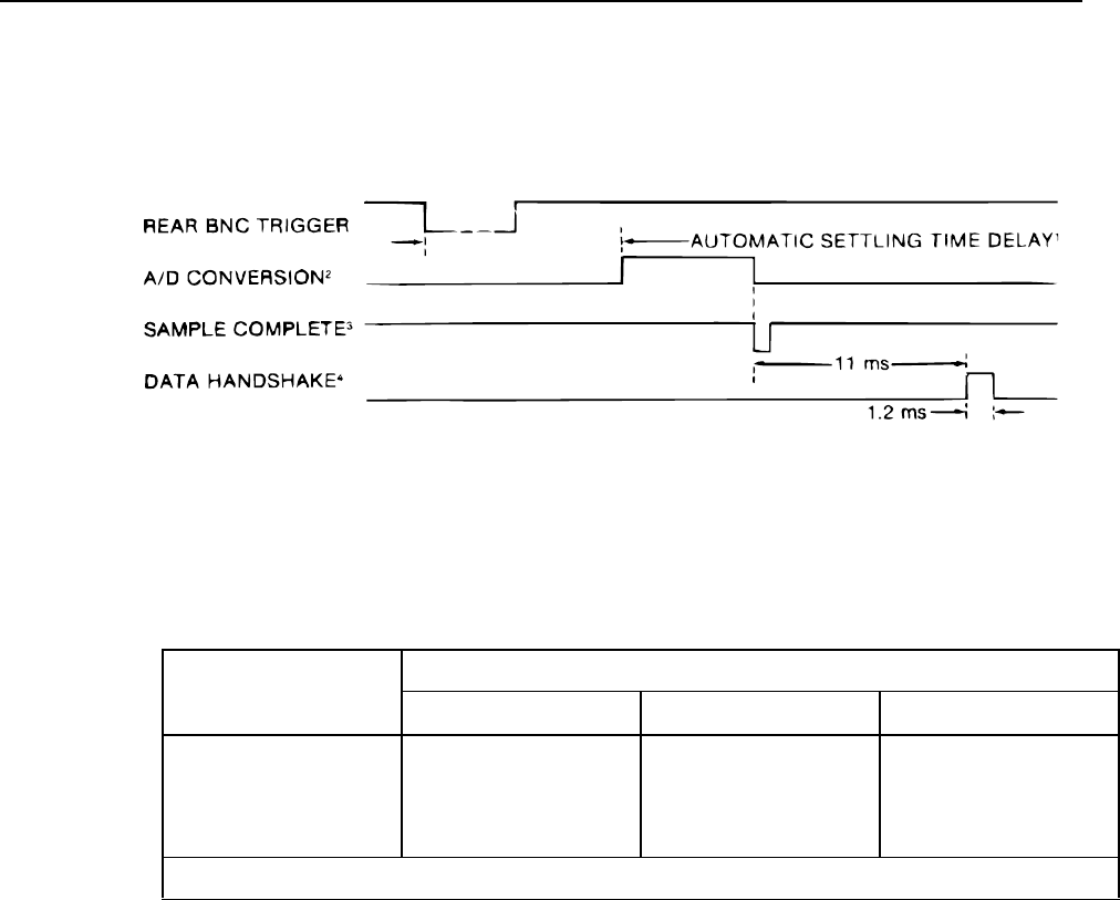
EXTERNAL TRIGGER TIMING CHARACTERISTICS
The following diagram shows the nominal timing for the various processes which take place between an
external trigger and data sent out on the IEEE-488 interface. Delays will vary if a second trigger comes
before the data handshake is complete.
t1-1.wmf
NOTES: 1. Time for single trigger to start of A/D conversion.(See “Automatic Settling Time
Delay” on previous page.) If the delay is disabled by using the T3 or T4 command,
then the delay is 1 ms±150 µs. When the 8842A is triggered with an IEEE-488
command (GET or ?), the automatic settling time delay begins after the trigger
command has been processed and recognized.
2. A/D conversion time is dependent on the reading rate and power-line frequency:
A/D CONVERSION TIME (ms)
RATE
50 Hz 60 Hz 400 Hz
S 472 (3800)* 395 (3195)* 414 (3300)*
M 52 (960)* 45 (795)* 47 (840)*
F777
*In 20 mV DC, 20Ω and 200 mA DC ranges.
3. Sample complete is a 2.5 µs pulse which indicates that the analog input may be
changed for the next reading.
4. When talking to a fast controller.
Introduction and Specifications
SPECIFICATIONS
1
1-11
GENERAL
COMMON MODE VOLTAGE..................1000V dc or peak ac, or 700V rms ac from any input to earth.
TEMPREATURE RANGE .......................0 to 50°C operating, -40 to 70°C storage.
HUMIDITY RANGE.................................80% RH from 0 to 35°C, 70% to 50°C.
WARMUP TIME......................................1 hour to rated specifications.
POWER ..................................................100, 120, 220, or 240V ac ±10% (250V ac maximum), switch
selectable at rear panel. 50, 60, or 400 Hz, automatically
sensed at power-up. 20 VA maximum.
VIBRATION.............................................Meets requirements of MIL-T- 28800C for Type III, Class 3,
Style E equipment.
PROTECTION ........................................ANSI C39.5 AND IEC 348, Class I.
SIZE........................................................8.9 cm high, 21.6 cm wide, 37.1 cm deep(3.47 in high, 8.5 in
wide, 14.6 in deep).
WEIGHT..................................................Net, 3.4 kg (7.5 lb); shipping, 5.0 kg (11 lb).
INCLUDED..............................................Line cord, test leads, Instruction/Service Manual, IEEE-488
Quick Reference Guide, (Option –05 only), and instrument
performance record.
IEEE-488 INTERFACE FUNTION ..........Option allows complete control and data output capability, and
supports the following interface funtion subsets: SH1,AH1, T5,
L4, SR1, RL1, DC1, DT1, E1, PP0, AND C0.
ELECTROMAGNETIC COMPATIBILITYSpecifications apply when used in an environment with fields
strengths ≤ 1 V/m, (0.8 V/m for DC Current.) For fields
strengths up to 3 V/m, multiply floor adder by 12 for VDC and
Resistance and 200 for DC current. VAC and AC Current have
no adders up to 3 V/m.
f1-01.wmf
Figure 1-1. External Dimensions
2-1
Chapter 2
Operating Instructions
Title Page
2-1. INTRODUCTION................................................................................2-2
2-2. INSTALLATION.................................................................................2-2
2-3. Installing the Power-Line Fuse ........................................................2-2
2-4. Connecting to Line Power................................................................2-2
2-5. Adjusting the Handle........................................................................2-3
2-6. Rack Mounting Kits.........................................................................2-3
2-7. OPERATING FEATURES ..................................................................2-4
2-8. Power-Up Features...........................................................................2-4
2-9. Front and Rear Panel Features .........................................................2-4
2-10. Display Features...............................................................................2-8
2-11. Error Messages.................................................................................2-8
2-12. Overrange Indication........................................................................2-10
2-13. Diagnostic Self-Tests .......................................................................2-10
2-14. Ranging ............................................................................................2-10
2-15. AUTORANGE.............................................................................2-10
2-16. MANUAL RANGE.....................................................................2-11
2-17. Triggering.........................................................................................2-11
2-18. CONTINUOUS TRIGGER MODE ............................................2-11
2-19. EXTERNAL TRIGGER MODE .................................................2-11
2-20. Reading Rates and Noise Rejection .................................................2-11
2-21. Automatic Settling Time Delay........................................................2-12
2-22. External Trigger Input (Option -05 Only)........................................2-12
2-23. Sample Complete Output (Option -05 Only) ...................................2-12
2-24. MAKING MEASUREMENTS............................................................2-13
2-25. Input Overload Protection Limits.....................................................2-13
2-26. Measuring Voltage and Resistance ..................................................2-13
2-27. Measuring Current ...........................................................................2-13
2-28. Current Fuse Protection....................................................................2-13
2-29. Offset Measurements .......................................................................2-14
2-30. EXTERNAL CLEANING....................................................................2-15
8842A
Instruction Manual
2-2
2-1. INTRODUCTION
This section provides instructions for installing and operating the 8842A. Refer to
Section 4 for measurement considerations.
2-2. INSTALLATION
2-3. Installing the Power-Line Fuse
WARNING
FOR POWER-LINE VOLTAGES OF 198V TO 250V, THE POWER-
LINE FUSE MUST BE REPLACED WITH A 1/8A, 250V SLO-BLO
FUSE FOR FIRE PROTECTION. TO AVOID ELECTRIC SHOCK,
REMOVE THE POWER CORD BEFORE REPLACING THE
EXTERNAL LINE FUSE.
The 8842A has a rear-panel power-line fuse in series with the power supply. A 1/4A,
250V slow-blow fuse is installed in the factory for operation from 90V to 132V. For
operation with power-line voltages of 198V to 250V, the fuse must be replaced with a
1/8A, 250V slo-blow fuse.
To replace the power-line fuse, first remove the power cord. Then turn the rear-panel fuse
cover 1/4-turn counterclockwise with a screwdriver.
For power-line voltages of 198V to 250V, use only a 1/4 x 1 1/4 (6.3mm x 32mm) fuse
with at least a 100A breaking capacity.
2-4. Connecting to Line Power
WARNING
TO AVOID SHOCK HAZARD, CONNECT THE INSTRUMENT
POWER CORD TO A POWER RECEPTACLE WITH EARTH
GROUND. TO AVOID INSTRUMENT DAMAGE, CHECK THAT
THE REAR PANEL LINE VOLTAGE SELECTION SWITCHES ARE
SET TO THE POWER-LINE VOLTAGE IN OUR AREA.
The 8842A can be configured to accept line power of 100, 120, 220, or 240V ac (+/-10%,
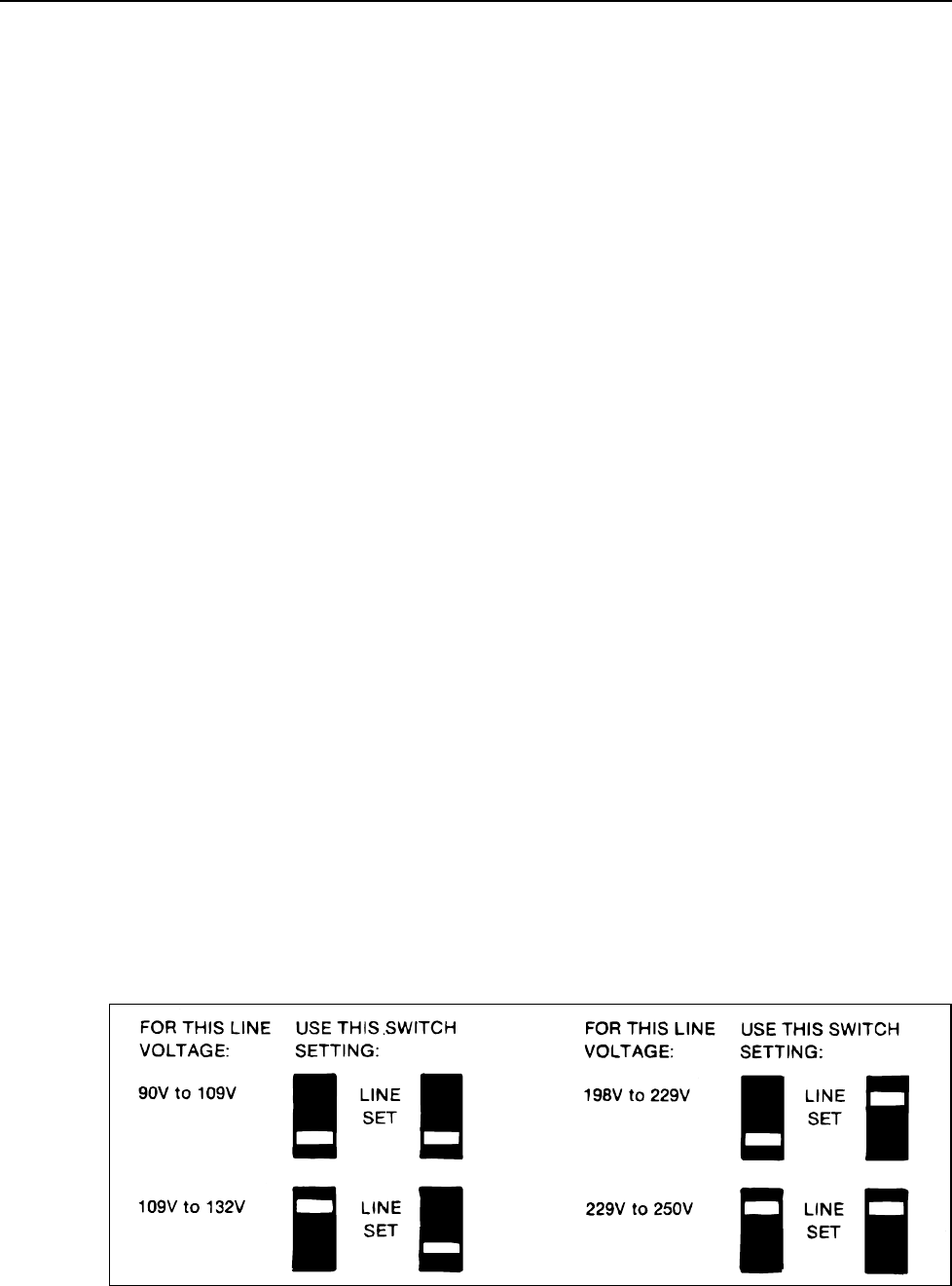
250V maximum) at 50, 60, or 400 Hz. The voltage must be selected by setting the rear
panel LINE SET switches as shown in Figure 2-1. The 8842A automatically senses the
power-line frequency at power-up, so that no adjustment for frequency is necessary.
f2-01.wmf
Figure 2-1. Line Voltage S election Settings
Operating Instructions
INSTALLATION
2
2-3
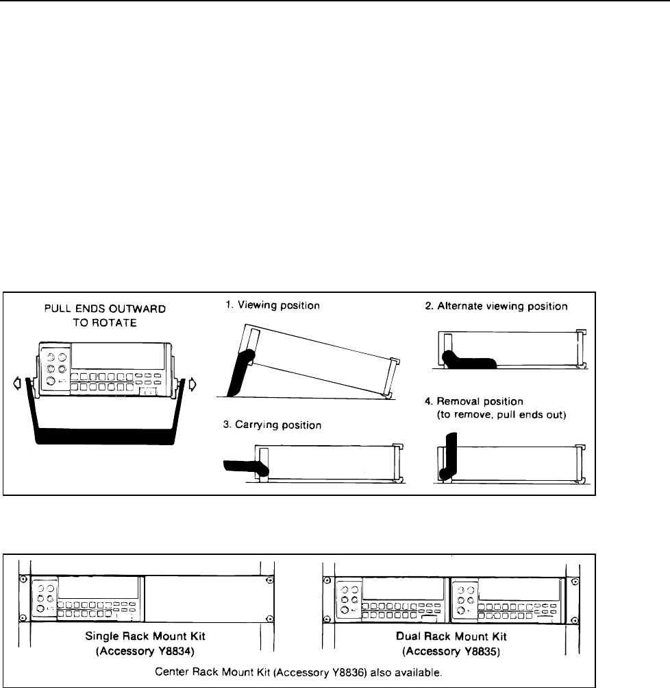
2-5. Adjusting the Handle
The handle provides two viewing angles for bench-top use. To adjust its position, pull the
ends out to a hard stop (about 1/4 inch on each side) and rotate it to one of the four stop
positions shown in Figure 2-2. To remove the handle, adjust it to the vertical stop
position and pull the ends all the way out.
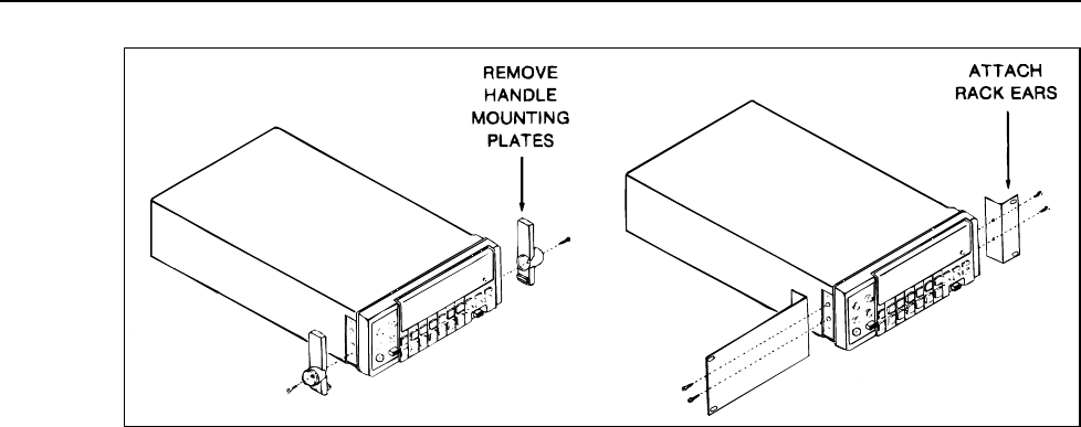
2-6. Rack Mounting Kits
You can mount the 8842A in a standard 19-inch rack panel using the accessory rack
mounting kits shown in Figure 2-3. To install the Single Rack Mount Kit, remove the
handle and handle mounting plates, and attach the rack ears with the screws provided
(Figure 2-4). The Dual Rack Mount Kit is installed similarly. (Both kits include mounting
instructions.)
The rear feet may be rotated 180 degrees to clear a narrow rack space.
f2-02.wmf
Figure 2-2. Adjusting the Handle
f2-03.wmf
Figure 2-3. Rack-Mount Kits
8842A
Instruction Manual
2-4
f2-04.wmf
Figure 2-4. Installing the Single Rack Mount Kit
2-7. OPERATING FEATURES
2-8. Power-Up Features
When the 8842A is turned on, all display segments light up for about 2 seconds while the
instrument performs an internal self-test of its digital circuitry. The 8842A then assumes
the following configuration:
• VDC function
• Autorange, starting in the 1000V range
• Slow reading rate
• Continuous, internal trigger
• OFFSET off
• Local (front panel) control
While all display segments are lit during the power-up self-test, you can freeze the
display by pressing the SRQ button. All display segments will then remain lit until you
press any button.
2-9. Front and Rear Panel Features
Front panel features are explained in Figure 2-5. Rear panel features are explained in
Figure 2-6.
The alternate functions embossed below the front panel range buttons and the special
feature buttons are enabled by the CAL ENABLE switch. These functions are for use
only when calibrating the instrument. See the Maintenance section for further
explanation.
CAUTION
To avoid accidentally uncalibrating the 8842A, do not press the
CAL ENABLE switch unless calibrating the instrument. Never
cycle power on or off while the CAL ENABLE switch is on.
Operating Instructions
OPERATING FEATURES
2
2-5
Note that the VAC and mA AC functions are available only with the True RMS AC
option. If this option is absent, pressing the VAC and mA AC function buttons causes the
8842A to briefly display an error message (ERROR 30).
!
!
M
FUNCTION BUTTONS:
RANGE BUTTON:
DC Volts
AC Volts*
2-Wire Ohms
4-Wire Ohms
Display
HIGH and LO SENSE
Terminals for 4-Wire Ohms Only
HI and LO
INPUT Terminals
2A INPUT Terminal
(Houses 2A fuse)
FRONT/REAR switch selects
either front or rear inputs.
Calibration Functions
(embossed)
*Available with 8842A-09 True RMS AC only.
Gives error message if option not installed.
** For a description of the autorange feature,
see paragraph 2-14.
20 mV or 20
200 mV or 200
2V or 2 k 20 M
20V or 20 k Autorange On/Off **
200V, 200 k or
200 mA dc
1000V dc, 700V ac,
2 M or 2000 mA
POWER switch turns 8842A
on or off. Also initiates
power-up self-test and
resets instrument to:
VDC function
Autorange
Slow reading rate
Continuous trigger
OFFSET off
Local (front panel) control
SPECIAL
FEATURES
CAL ENABLE switch
enables calibration
mode. (CAUTION! See text.)
DC Current
AC Current*
f2-05_1.wmf
Figure 2-5. Front Panel Features
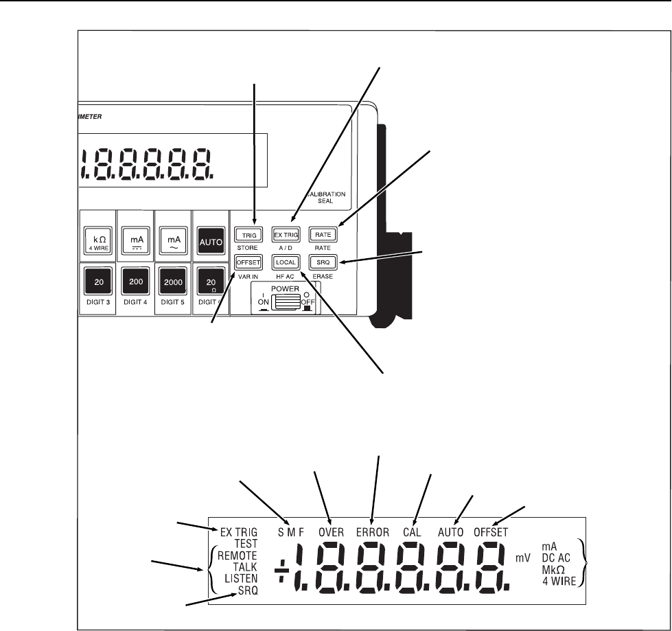
8842A
Instruction Manual
2-6
M
TRIG triggers a new reading.
Enabled in external trigger mode.
EXT TRIG toggles between internal
and external trigger modes
RATE cycles between slow, medium and
fast reading rates. Automatically
selects the optimum filter for each
reading rate.
SRQ generates a service request over the IEEE-
488 bus if enabled by the SRQ mask (IEEE-488
Interface option only). When pressed for 3
seconds, SRQ initiates diagnostic self-tests.
NOTE: Leave inputs disconnected during self-
tests or the 8842A may indicate errors.
OFFSET stores the displayed reading as an
offset, which the 8842A subtracts from all
subsequent readings in the function
presently selected. Readings in the other
functions remain unaffected. Pressing
OFFSET again cancels the offset, or stores
a new offset if in a different function.
If the 8842A is in remote, LOCAL returns it to
local control. If the 8842A is in local, the
LOCAL button causes the 8842A to display its
bus address for two and one half seconds.
Ignored if the IEE-488 Interface is not
installed.
Self-Test
Enabled
Calibration Mode Enabled
Error Condition
Overrange
Autorange On
Offset On
Function
and Units
Annunciators
Reading Rate Slow, Medium
and Fast. Blinks off when a
reading is triggered.
External Trigger
Mode Enabled
IEEE-488 Interface
Annunciators
f2-05_2.wmf
Figure 2-5. Front Panel Features (cont)
Operating Instructions
OPERATING FEATURES
2
2-7
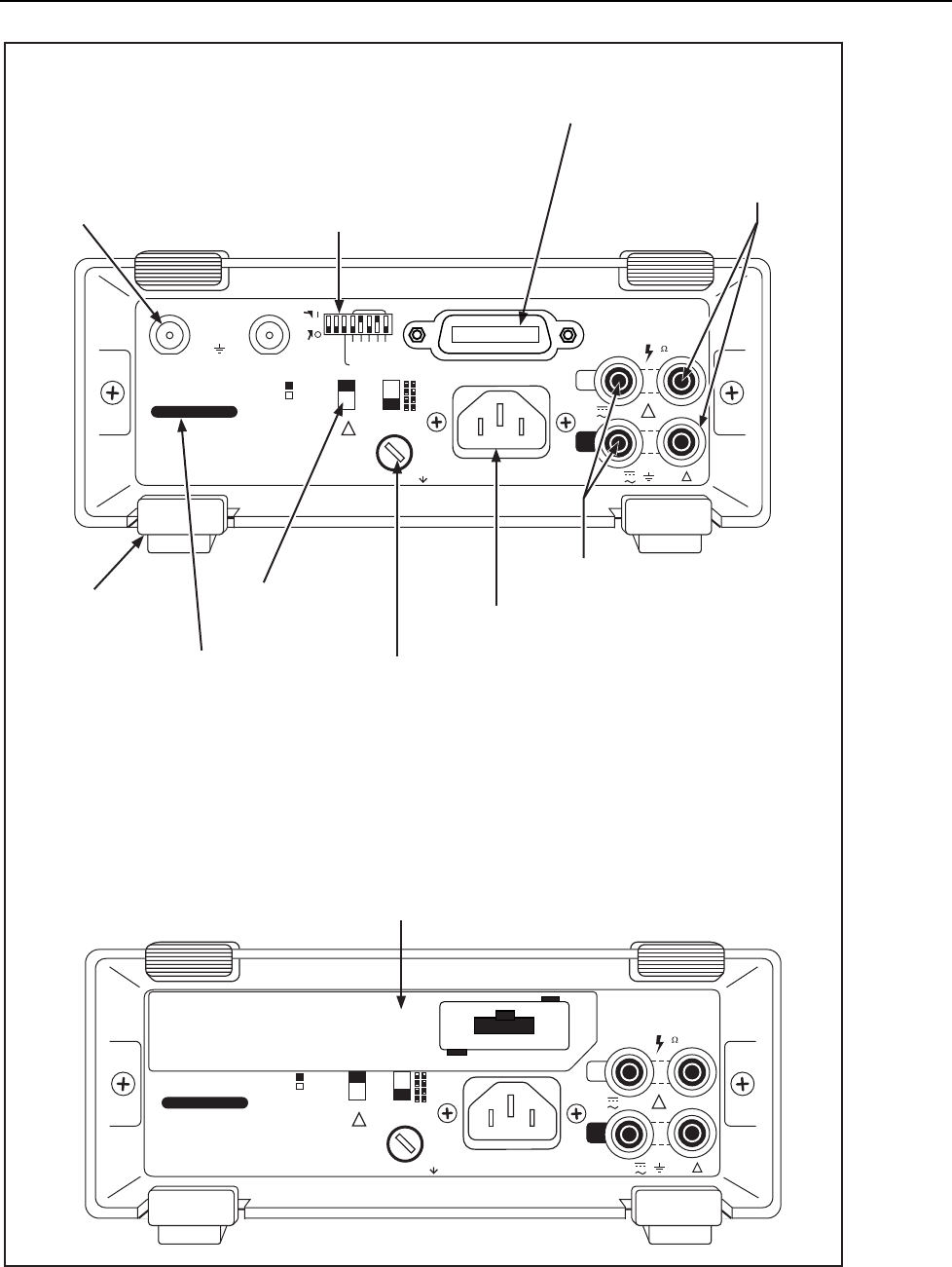
Line Voltage
Selection Switches
Power-Line Fuse
Power-Line Cord
Connector
HI and LO INPUT
Terminals
IEEE-488 Interface
Bus Connector*
TALK ONLY and IEEE-488
ADDRESS Selection Switches*
SAMPLE COMPLETE output
TTL-level. Normally high,
pulsed low when samples for
a reading are completed*
*Available with IEEE-488 Interface only.
Otherwise, the upper portion of the rear panel is
covered with an insert as shown at right.
CAUTION: The rear panel insert is attached from
inside the case. Refer to Section 8 for instructions
on removing it.
EX TRIG input*
TTL-level,
falling-edge triggered
(internally selectable)
Serial Number
Rear feet rotate
for rack mounting
Rear Panel Insert
HIGH and LO SENSE
Terminals for 4-Wire
Ohms Only
IEEE STD-488 PORT
SH1, AH1, T5, L4, SR1, RL1,
DC1, DT1, PP0, C0, E1
INPUT SENSE
300V MAX
1000V
700V
1000V
700V
HI
4 WIRE
20 VA 50/60/400 Hz
A5
TALK
ONLY
SAMPLE
COMPLETE
SHELL NOT
GROUNDED
15V MAX
PATENTS PENDING
IN OUT
IEEE-05
AC-09
EXT TRIG
10V MAX
TTL LEVELS
JOHN FLUKE MFG. CO., INC.
EVERETT, WA MADE IN U.S.A.
!
REMOVE GROUNDING SCREW BEFORE REMOVING COVER
ADDRESS
A3
240V
220V
120V
100V
LINE
SET
LINE FUSE
250V
CAUTION
FOR FIRE PREVENTION
REPLACE ONLY WITH
1/4 A SLOW FUSE, 100/120v
1/8 A SLOW FUSE, 220/240V
WARNING
GROUNDING CONDUCTOR
IN POWER CORD MUST BE
CONNECTED TO ENSURE
PROTECTION FROM
ELECTRICAL SHOCK
A1
!
!
LO
MAX
MAX
ALL
INPUTS
INPUT SENSE
300V MAX
1000V
700V
1000V
700V
HI
4 WIRE
20 VA 50/60/400 Hz
PATENTS PENDING
IEEE-05
AC-09
JOHN FLUKE MFG. CO., INC.
EVERETT, WA MADE IN U.S.A.
!
REMOVE GROUNDING SCREW BEFORE REMOVING COVER
240V
220V
120V
100V
LINE
SET
LINE FUSE
250V
CAUTION
FOR FIRE PREVENTION
REPLACE ONLY WITH
1/4 A SLOW FUSE, 100/120v
1/8 A SLOW FUSE, 220/240V
WARNING
GROUNDING CONDUCTOR
IN POWER CORD MUST BE
CONNECTED TO ENSURE
PROTECTION FROM
ELECTRICAL SHOCK
!
!
LO
MAX
MAX
ALL
INPUTS
f2-06.wmf
Figure 2-6. Rear Panel Features
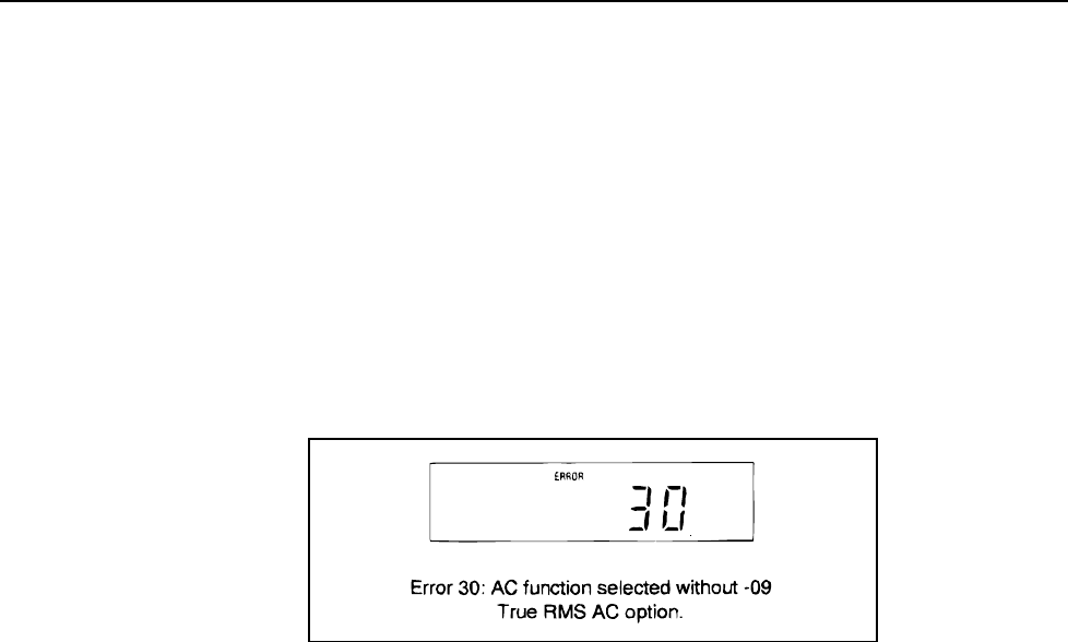
8842A
Instruction Manual
2-8
2-10. Display Features
The 8842A features a vacuum fluorescent display with a numeric field and annunciators.
The annunciators are explained in Figure 2-5.
2-11. Error Messages
If the 8842A detects an operator error or an internal failure, it displays an error message
for about 2-1/2 seconds and then resumes normal operation. During this time, the front
panel buttons are ignored. The error message consists of the ERROR annunciator and a
two-digit error code. (See Figure 2-7.) Error codes are explained in Table 2-1.
If the FRONT/REAR switch is set to the REAR position while the mA DC or mA AC
function is selected, ERROR 31 is displayed. In this case the error message is displayed
until you return the switch to the FRONT position or select another function.
f2-07.wmf
Figure 2-7. Typical Error Messages
Operating Instructions
OPERATING FEATURES
2
2-9
Table 2-1. Error Codes
ERROR
CODE MEANING ERROR CODE MEANING
ANALOG SELF-TEST ERRORS OPERATION ERRORS
1 200 VAC, Zero 30 AC funtions availible only with 8842A-09 True
RMS AC option.
2 700 VAC, Zero 31 mA AC or mA DC funtion selected while
REAR inputs selected.
3 mA AC, Zero 32 OFFSET selected with reading unavailible for
overrange.
4 mA DC, Zero 40 Computed calibration constant out of
range.(Previous cal may be wrong or there
may be a hardware problem.)
5 200 VDC, Zero 41 Calibration input out of acceptable range.
Check that input is correct. (Previous cal may
be wrong or there may be a hardware
problem.)
6 1000 VDC, Zero 42 Calibration memory write error. (Probably a
hardware problem.)
7 1000 VDC, Zero 50 Guard crossing error detected by In-Guard
µC.
8 20 VDC + 20MΩ51 Calibration command not valid unless
calibration mode is enabled.
9 20 VDC + 2000 kΩ52 Command not valid at this time.
10 2 VDC + 2000 kΩ53 Invalid calibration value in Put command.
(Example: Sending a negative value during
ac calibration.)
11 200Ω, Overrange 54 Command not valid in calibration verification.
12 2 kΩ, Overrange 56 Variable inputs not allowed during A/D
calibration.Use prompted value.
13 20 kΩ, Overrange 60 Device-dependent commands not valid
during self-tests.
14 200 kΩ, Overrange 71 Syntax error in device-dependent command
string.
15 1000 VDC + X10 T/H + 20 MΩ72 Guard crossing error detected by out Guard
µC.
16 200 VDC + 200 kΩ73 Guard crossing error detected at power on or
CAL ENABLE switch on at power on.
17 200 VDC + 20 kΩ77 IEEE-488 Interface self-test error.
DIGITAL SELF-TEST ERRORS
25 In-Guard µC Internal RAM
26 Display RAM
27 In-Guard µC Internal Program Memory
28 External Program Memory
29 Calibration Memory
NOTE: See the Maintenance section for a detailed description of self-tests.

8842A
Instruction Manual
2-10
2-12. Overrange Indication
An input is overrange if it exceeds the full scale of the selected range. In most ranges, the
8842A indicates an input is overrange by lighting the OVER annunciator and showing a
"1" on the display. (See Figure 2-8.) The sign, the position of the decimal point, and the
other annunciators are not affected.
As a safety feature, the 8842A treats the 1000V dc and 700V ac rangesdifferently. In
these ranges, the 8842A indicates when the input exceeds the input overload limit of
1000V dc or 700V ac, respectively, by lighting the OVER annunciator and flashing the
display. Readings are still displayed.
2-13. Diagnostic Self-Tests
The 8842A features diagnostic self-tests which check both the digital and analog circuitry
in the instrument. The self-tests consist of 21 analog tests followed by the in-guard
program memory, calibration memory, and display self-tests. To initiate the self-tests,
press the SRQ button for 3 seconds. The instrument can be stopped in any of the test
configurations by pressing the SRQ button while the test number is displayed. Press any
button to continue the tests.
During the test, the TEST annunciator lights, and the numeric field displays the number
of each analog test as it is performed. Then all display segments light up while the
instrument performs the in-guard program memory, calibration memory, and display self-
tests. The 8842A then returns to the power-up configuration. The self-tests are described
in greater detail in the Maintenance section.
NOTE
The inputs must be left disconnected while the self-tests are performed or
the 8842A may indicate that errors are present.
If the 8842A detects an error, it displays an error message for about 2-1/2 seconds. (Error
codes 01 through 29 correspond to the self-tests.) If self-test errors are displayed even
when the input terminals are disconnected, there may be a hardware problem in your
8842A. In that event, refer to the Maintenance section or contact your local Fluke
representative.
2-14. Ranging
Measurement ranges can be selected using either autorange (by pressing the AUTO
button) or manual range (by pressing another range button). The 8842A displays explicit
units in every range, so that the display may be read directly.
2-15. AUTORANGE
In autorange, the 8842A goes to a higher range when the input exceeds full scale (199999
counts), and goes to a lower range when the input falls below 9% of full scale (18000
counts). While the instrument changes range, the numeric field on the display is blanked
until a new reading is completed. However, the decimal point and units annunciators
always indicate what range the instrument is in.
Pressing the AUTO button when the instrument is already in autorange toggles the
8842A from autorange to manual range. This causes the instrument to remain locked in
the present range.
The 8842A autoranges up to the highest ranges in all functions, down to the 200 mV
range in the VDC and VAC functions, and down to the 200Ω range in the ohms
functions. To select the 20 mV dc, 20Ω, or 200 mA dc range, press the respective range
button (or send the respective range command, if using the IEEE-488 option).

Operating Instructions
OPERATING FEATURES
2
2-11
2-16. MANUAL RANGE
In manual range, the 8842A remains fixed in the selected range until you select another
range or press AUTO. If you select a range which is not valid for the present function, or
select a function which is not valid for the present range, the 8842A selects the nearest
valid range. For example, if the 8842A is in the VDC function and you press the 20 MΩ
button, the 8842A selects the 1000V range.
The range buttons have no effect in the mA AC functions, since all measurements in
these functions are made in the 2000 mA range.
2-17. Triggering
Triggering causes the 8842A to execute a measurement cycle and display the result.
During each measurement cycle, the instrument samples the input a number of times and
then averages the samples to compute a reading. The number of samples averaged for
each reading depends upon the reading rate.
Each time a reading is triggered, the rate annunciator (S, M, or F) blinks off. In the fast
reading rate, the F annunciator flashes so rapidly it appears to be almost constant.
How the 8842A is triggered depends on whether the continuous trigger mode or external
trigger mode is selected. Pressing the EX TRIG (external trigger) button toggles the
8842A between the two modes.
2-18. CONTINUOUS TRIGGER MODE
In the continuous trigger mode, readings are triggered by a continuous, internal trigger.
The rate of the trigger is set by the RATE button.
2-19. EXTERNAL TRIGGER MODE
In the external trigger mode, readings are triggered by pressing the TRIG button. If the
IEEE-488 Interface option is installed, readings can also be triggered by remote
commands or by using the rear panel external trigger (EXT TRIG) connector. (See the
Options and Accessories section.)
In the external trigger mode, pressing any front panel button blanks the numeric field on
the display until a new measurement is triggered. This ensures that all readings
correspond to the instrument configuration indicated by the display annunciators. The
blanking also occurs in the continuous trigger mode, but usually isn’t noticed because
new measurements are triggered automatically.
The TRIG button does not trigger readings in the continuous trigger mode.However, it
does blank the last reading to acknowledge a button was pressed.
2-20. Reading Rates and Noise Rejection
The RATE button allows you to optimize either measurement speed or noise rejection.
The 8842A uses both analog and digital filtering to allow measurements in the presence
of unwanted environmental noise (especially line-related noise). However, since filtering
introduces a delay in response to a change in the input signal, there is an inherent trade-
off between noise rejection and measurement speed.
The instrument has three reading rates: slow (S) and medium (M), with a 5-1/2 digit
display, and fast (F), with a 4-1/2 digit display. To provide optimum combinations of
measurement speed and noise rejection, the RATE button allows control of both the
internal trigger rate and the degree of filtering. The same degree of filtering is used in
both the continuous and external trigger modes. In the 20 mV, 20Ω, and 200 mA dc
ranges, use of slow (S) filter provides maximum noise rejection.
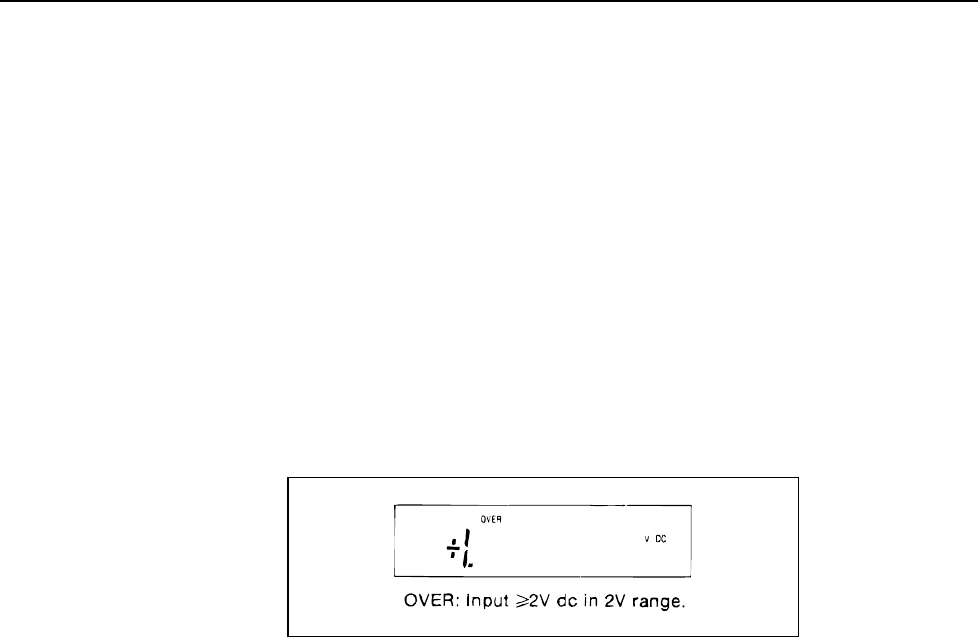
8842A
Instruction Manual
2-12
In the continuous trigger mode, the actual number of readings displayed per second for
each reading rate is determined by the line-power frequency. At power-up, the 8842A
senses the line-power frequency and adjusts the analog-to-digital converter timing
characteristics for optimum normal-mode noise rejection. The resulting reading rates are
shown in the specifications in Section 1.
2-21. Automatic Settling Time Delay
When the external trigger mode is selected, the 8842A automatically inserts a delay after
receiving a trigger signal, but before starting the first input sample. The delay is just long
enough so that the reading will be correct (within a specified number of counts of the
final value) even if the trigger signal occurs as the input makes a step change between
zero and full scale (10,000 counts and full scale in the ac functions).The length of the
delay depends on the range, function, and reading rate, as shown in the specifications in
Section 1. The delay is enabled only in the external trigger mode. It can be turned off
with a remote command over the IEEE-488 interface bus to accommodate special timing
considerations.
f2-08.wmf
Figure 2-8. Overrange Indication
2-22. External Trigger Input (Option -05 Only)
The rear panel EXT TRIG input is a TTL-level input which can be used to trigger
measurements when the 8842A is in the external trigger mode. A measurement is
triggered on the falling edge of the input. Since the EXT TRIG input is pulled high
internally, it can also be controlled by a normally open switch. A measurement is
triggered when the switch is closed. For special applications using the IEEE-488
Interface, the automatic setting time delay can be disabled using remote commands. (See
Section 3.) Refer to Section 1 for timing details.
The polarity of the EXT TRIG input can be reversed by changing internal jumpers. Refer
to the Maintenance section for instructions.
2-23. Sample Complete Output (Option -05 Only)
The SAMPLE COMPLETE output indicates when analog input sampling for a reading is
completed. The output is a TTL-level signal which is pulsed low for approximately 2.5
µs when the input-sampling portion of the A/D conversion is completed. The signal is
useful for interfacing with other equipment when the 8842A is used in external trigger
mode in an instrumentation system. For example, the SAMPLE COMPLETE output
could be used to advance a scanner to the next channel.
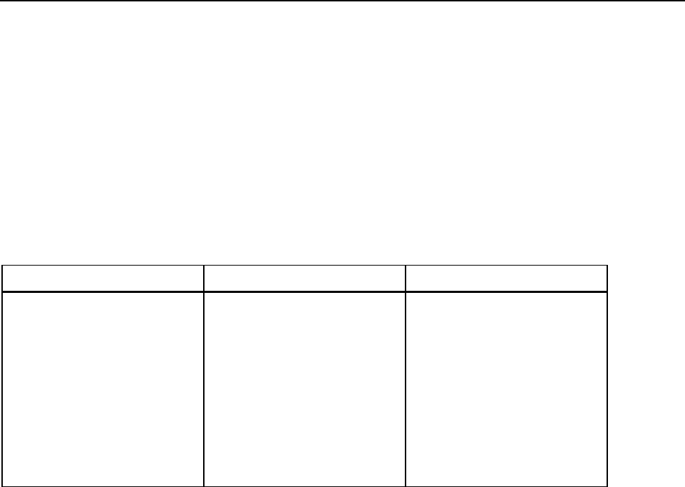
Operating Instructions
MAKING MEASUREMENTS
2
2-13
2-24. MAKING MEASUREMENTS
2-25. Input Overload Protection Limits
WARNING
TO AVOID SHOCK HAZARD AND/OR INSTRUMENT DAMAGE,
DO NOTAPPLY INPUT POTENTIALS THAT EXCEED THE INPUT
OVERLOAD LIMITS SHOWN IN TABLE 2-2.
The 8842A is protected against input overloads up to the limits shown in Table 2-2.
Exceeding these limits may damage the instrument and/or pose a shock hazard.
Table 2-2. Input Overload Limits
FUNTION CONNECTORS MAXIMUM INPUT
VDC INPUT HI and LO: 1000 dc
MA DC 2A INPUTand INPUT LO: 2000mA
2 WIRE/4 WIRE kΩINPUT HI and LO: 300V rms
SENSE HI and LO: 300V rms
VAC INPUT HI and LO: 700V rms, 1000V peak, or 2 x 10⁷
V-Hz (whichever is less)
MA AC 2A INPUT and INPUT LO: 2000 mA rms
All Funtions Any terminal to earth: 1000V dc or peak ac
2-26. Measuring Voltage and Resistance
To measure voltage or resistance, select the desired function and connect the test leads as
shown in Figure 2-9. Resistance can be measured in either the 2-wire or 4-wire
configuration.
2-27. Measuring Current
To measure current, select the desired function and connect the test leads as follows:
1. Turn off power in the circuit to be measured (Figure 2-10).
2. Break the circuit (preferably on the ground side to minimize the common mode
voltage), and place the 8842A in series at that point.
3. Turn on power in the circuit, and read the display.
4. Turn off power in the circuit, and disconnect the 8842A.
2-28. Current Fuse Protection
The 2A input terminal is protected from overloads by a 2A, 250V fuse which is
accessible from the front panel, and by an internal 3A, 600V fuse. If either fuse blows,
the 8842A will respond as though the input were zero.
WARNING
TO AVOID ELECTRIC SHOCK, REMOVE THE TEST LEADS
BEFOREREPLACING THE FRONT PANEL FUSE.

8842A
Instruction Manual
2-14
To replace the front panel fuse, first remove the test leads. Then press in the lip of the 2A
input terminal slightly and rotate it 1/4-turn counterclockwise. Spring tension will force
the fuse and fuse holder out of the front panel. The internal 3A fuse should be replaced
only by qualified service personnel.
2-29. Offset Measurements
WARNING
WHEN THE OFFSET FEATURE IS IN USE, DISPLAYED
READINGS ARE RELATIVE AND MAY NOT INDICATE THE
PRESENCE OF DANGEROUS POTENTIALS AT THE INPUT
CONNECTORS OR TEST LEADS. USE CAUTION TO AVOID
ELECTRIC SHOCK OR INSTRUMENT DAMAGE.
The OFFSET feature allows you to store a reading as a relative reference value. When the
OFFSET button is pressed, the 8842A stores the present reading and displays subsequent
measurements as the difference between the measured value and the stored reading. The
OFFSET annunciator is lit whenever an offset is in use.
The OFFSET feature may be used in all functions. Since the display represents a numeric
difference, it always has a sign, even in the resistance and ac functions.
The offset can be canceled by pressing the OFFSET button again, in which case the
OFFSET annunciator disappears from the display. The offset can also be canceled by
storing an offset in another function. If a reading is overrange or unavailable when the
OFFSET button is pressed, the 8842A indicates ERROR 32 and does not store the offset.
If you change functions while an offset is stored, the OFFSET annunciator disappears and
the offset temporarily disappears. However, when you return to the original function, the
offset is restored (and the OFFSET annunciator reappears) unless a new offset was
established in another function. Note that the input overload limits are not changed by the
use of the offset feature. However, the display flashes if the 8842A is in the 1000V dc or
700V ac ranges and the input exceeds 1000V dc or 700V ac, respectively.
While an offset is enabled, the 8842A indicates an overrange condition if either of the
following conditions occur:
• The input signal is overrange
• The calculated reading is overrange
For example, suppose the instrument is in the 20V range of the VDC function and you
store an offset of +15V. The maximum positive voltage reading that can be displayed
without overranging is +4.9999V, which is actually a +19.9999V input signal. The
maximum negative voltage reading that can be displayed without overranging is -
19.9999V, which is actually a -4.9999V input signal. You can measure a greater range of
voltages by selecting a higher range.
When in autorange, the 8842A selects the range appropriate for the input signal,
regardless of any stored offset. If, for example, a +10V offset is stored, and a +1V input
is applied, the 8842A will autorange to the 2V range and display an overrange condition
since it cannot display -9V on the 2V range. Manual range control could be used to lock
the 8842A into the 20V range in this case.
Applications of the offset feature include correcting for test lead resistance in 2-wire
resistance measurements, nulling offset currents or voltages, measuring voltage
deviations, and matching resistors.
Operating Instructions
EXTERNAL CLEANING
2
2-15
f2-09.wmf
Figure 2-9. Measuring Voltage and Resistance
f2-10.wmf
Figure 2-10. Measuring Current
2-30. EXTERNAL CLEANING
WARNING
TO AVOID ELECTRIC SHOCK OR INSTRUMENT DAMAGE,
NEVER GET WATER INSIDE THE CASE. TO AVOID
INSTRUMENT DAMAGE, NEVER APPLY SOLVENTS TO THE
INSTRUMENT.
Should the 8842A case require cleaning, wipe the instrument with a cloth that is lightly
dampened with water or a mild detergent solution.

8842A
Instruction Manual
2-16
3-1
Chapter 3
Remote Programming
Title Page
3-1. INTRODUCTION................................................................................3-3
3-2. CAPABILITIES ...................................................................................3-3
3-3. BUS SET-UP PROCEDURE...............................................................3-3
3-4. AN OVERVIEW OF REMOTE OPERATION...................................3-4
3-5. A NOTE ABOUT EXAMPLES...........................................................3-6
3-6. DEVICE-DEPENDENT COMMAND SET ........................................3-6
3-7. Bn (Offset Commands) ....................................................................3-9
3-8. Cn (Calibration Commands) ............................................................3-9
3-9. Dn (Display Commands)..................................................................3-9
3-10. Fn (Function Commands) ................................................................3-10
3-11. Get Commands.................................................................................3-10
3-12. G0 (Get Instrument Configuration)..................................................3-12
3-13. G1 (Get SRQ Mask).........................................................................3-12
3-14. G2 (Get Calibration Prompt)............................................................3-12
3-15. G3 (Get User-Defined Message)......................................................3-13
3-16. G4 (Get Calibration Status)..............................................................3-13
3-17. G5 (Get IAB Status).........................................................................3-14
3-18. G6 (Get YW Status).........................................................................3-14
3-19. G7 (Get Error Status) .......................................................................3-14
3-20. G8 (Get Instrument Identification)...................................................3-15
3-21. N (Numeric Entry Command)..........................................................3-15
3-22. Put Commands .................................................................................3-15
3-23. P0 (Put Instrument Configuration)...................................................3-15
3-24. P1 (Put SRQ Mask)..........................................................................3-16
3-25. P2 (Put Calibration Value)..............................................................3-16
3-26. P3 (Put User-Defined Message)......................................................3-17
3-27. Rn (Range Commands)....................................................................3-17
3-28. Sn (Reading Rate Commands).........................................................3-17
3-29. Tn (Trigger Mode Commands) ........................................................3-18
3-30. Wn (Terminator Commands) ...........................................................3-19
3-31. X0 (Clear Error Register Command) ...............................................3-19
3-32. Yn (Suffix Commands)....................................................................3-19
3-33. Z0 (Self-Test Command) .................................................................3-19
3-34. (Device-Clear Command)................................................................3-20

8842A
Instruction Manual
3-2
3-35. ? (Single-Trigger Command) ...........................................................3-20
3-36. INPUT SYNTAX.................................................................................3-20
3-37. Definitions........................................................................................3-21
3-38. Input Processing...............................................................................3-21
3-39. Syntax Rules ....................................................................................3-23
3-40. OUTPUT DATA ..................................................................................3-24
3-41. Loading Output Data........................................................................3-24
3-42. Types of Output Data.......................................................................3-25
3-43. Numeric Data and Error Messages...................................................3-25
3-44. MEASUREMENT DATA...........................................................3-25
3-45. OVERRANGE INDICATION ....................................................3-26
3-46. ERROR MESSAGES ..................................................................3-26
3-47. Status Data .......................................................................................3-26
3-48. Output Priority .................................................................................3-26
3-49. SERVICE REQUESTS ........................................................................3-27
3-50. The Serial Poll Register ...................................................................3-27
3-51. The SRQ Mask.................................................................................3-28
3-52. INTERFACE MESSAGES ..................................................................3-29
3-53. Address Messages............................................................................3-29
3-54. Universal Commands.......................................................................3-29
3-55. Addressed Commands......................................................................3-30
3-56. TALK-ONLY MODE ..........................................................................3-30
3-57. REMOTE CALIBRATION..................................................................3-31
3-58. TIMING CONSIDERATIONS............................................................3-31
3-59. IMMEDIATE MODE COMMANDS..................................................3-31
3-60. EXAMPLE PROGRAMS ....................................................................3-32

Remote Programming
INTRODUCTION
3
3-3
NOTE
This section contains programming instructions for use with the IEEE-488
Interface (Option -05). For installation instructions, refer to the Options
and Accessories section.
3-1. INTRODUCTION
The IEEE-488 Interface turns the 8842A into a fully programmable instrument for use
with the IEEE Standard 488-1978 interface bus (IEEE-488 bus). With the IEEE-488
Interface, the 8842A can become part of an automated instrumentation system. The
8842A can be under complete, interactive control from a remote bus controller; or it can
be set to the talk-only mode, connected to a data logger or printer, and dedicated to a
single task.
This manual assumes you know the basics of the IEEE-488 interface bus. For an
introduction to the bus, request Fluke Application Bulletin AB-36, "IEEE Standard 488-
1978 Digital Interface for Programmable Instrumentation."
3-2. CAPABILITIES
The IEEE-488 Interface provides remote control of all front panel controls except for the
POWER, CAL ENABLE, and FRONT/REAR switches. Other features include:
• A simple and predictable command set
• Fast measurement throughput
• Full talk/listen capability, including talk-only operation
• Full serial poll capability, with bit-maskable SRQ
• Full remote/local capability, including local lockout
• EXTERNAL TRIGGER and SAMPLE COMPLETE connectors
• Remote calibration
• Programmable trigger sources, including two bus triggers
• Informative output suffix (suppressible)
• Selectable output terminators
The 8842A supports the following interface function subsets: SH1, AH1, T5, L4, SR1,
RL1, DC1, DT1, E1, PP0, and C0.
3-3. BUS SET-UP PROCEDURE
To set up the 8842A on the IEEE-488 bus, proceed as follows:
1. Turn the 8842A POWER switch OFF and set the 8842A IEEE-488 address using the
rear panel IEEE-488 address switches shown in Figure 3-1.
2. With the 8842A POWER switch OFF, plug the IEEE-488 cable into the 8842A rear
panel IEEE-488 connector.
3. Switch on the 8842A.
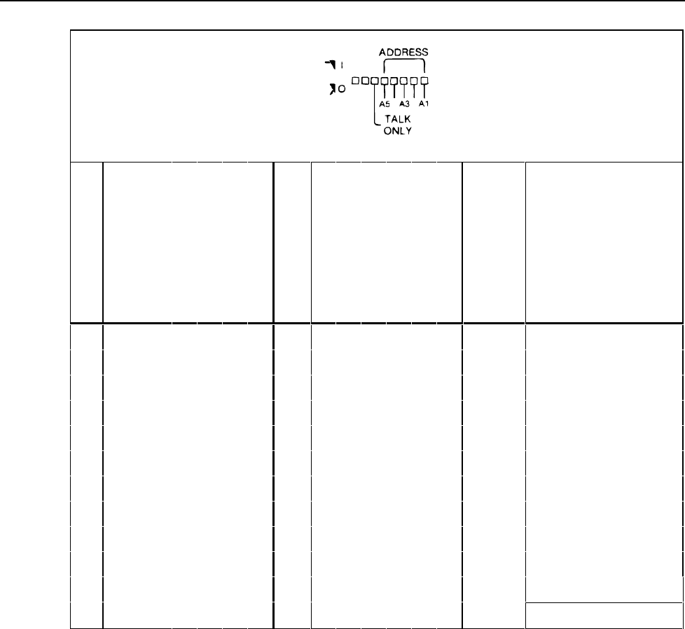
8842A
Instruction Manual
3-4
A
D
D
R
E
S
S
T
A
L
K
O
N
L
Y
A5 A4 A3 A2 A1 A
D
D
R
E
S
S
T
A
L
K
O
N
L
Y
A5 A4 A3 A2 A1 A
D
D
R
E
S
S
T
A
L
K
O
N
L
Y
A5 A4 A3 A2 A1
00 0 0 0000 11 001011 22 0 10110
01 0 0 0001 12 001100 23 0 10111
02 0 0 0010 13 001101 24 0 11000
03 0 0 0011 14 001110 25 0 11001
04 0 0 0100 15 001111 26 0 11010
05 0 0 0101 16 010000 27 0 11011
06 0 0 0110 17 010001 28 0 11100
07 0 0 0111 18 010010 29 0 11101
08 0 0 1000 19 010011 30 0 11110
09 0 0 1001 20 010100 31 Not allowed
10 0 0 1010 21 010101 1 XXXXXTALK
ONLY X = setting does not matter
f3-01.wmf
Figure 3-1. IEEE-488 Address Selection
Whenever the 8842A is in the local state, the IEEE-488 address can be displayed on the
front panel by pressing the LOCAL button.
3-4. AN OVERVIEW OF REMOTE OPERATION
An overview of remote operation is presented in the block diagram in Figure 3-2. Each
block represents a register, buffer, etc., contained in the 8842A. The status registers in the
center column indicate the instrument’s status, including its function, range, reading rate,
etc. The input buffer receives data from the IEEE-488 bus. The output buffer receives
data from the blocks to its left, and sends data on to the IEEE-488 bus.
Remote Programming
AN OVERVIEW OF REMOTE OPERATION
3
3-5
f3-02.wmf
Figure 3-2. Remote Operation Block Diagram
8842A
Instruction Manual
3-6
Information is transferred between blocks by device-dependent commands. Each
command is shown next to an arrowhead which indicates the resulting information
transfer. For example, Put command P0 takes a number from the input buffer and stores it
in the primary status registers. Likewise, Get command G0 gets the content of the
primary status registers and copies it into the output buffer.
3-5. A NOTE ABOUT EXAMPLES
In the examples in this manual, device-dependent commands are shown enclosed within
quotation marks, as they would be entered in Fluke BASIC. For clarity, the commands
are also separated by spaces. However, the spaces are are not necessary and may be
omitted.
Example Explanation
"* F3 R1 S1 T2" This example is equivalent to "*F3R1S1T2" or
"*,F3,R1,S1,T2".
Using the Fluke 1722A Instrument Controller, these commands might be written into a
BASIC program as shown in Figure 3-3. Examples using other controllers are given at
the end of this section.
f3-03.wmf
Figure 3-3. Typical Command String
Examples of 8842A output data show the terminators CR and LF. The terminator EOI is
not shown because it is a uniline message. However, the terminators CR, LF, and EOI are
all selectable using the Write commands.
For reference, the ASCII and IEEE Std 488-1978 bus codes are shown at the back of this
section.
3-6. DEVICE-DEPENDENT COMMAND SET
Device-dependent commands are the heart of 8842A remote control. They tell the 8842A
how and when to make measurements, when to put data on the bus, when to make service
requests, etc. Commands which correspond directly to the front panel controls or display
are shown in Figure 3-4. The complete set of device-dependent commands is listed in
Figure 3-5. The commands may be entered using either upper- or lower-case letters. See
Table 6-15 for conditions under which certain commands are not valid.
Remote Programming
DEVICE-DEPENDENT COMMAND SET
3
3-7
RANGE COMMANDS
R0 Autorange On
R1 200 mV, 200Ω
R2 2V, 2 kΩ
R3 20V, 20 kΩ
R4 200V, 200 kΩ, 200 mA
R5 1000V dc, 700V ac,
2 MΩ, 2000 mA
R6 20 MΩ
R7 Autorange Off
R8 20 mV, 20Ω
FUNCTION COMMANDS
F1 VDC
F2 VAC
F3 2 Wire kΩ
F4 4 Wire kΩ
F5 mA DC
F6 mA AC
DISPLAY COMMANDS
D0 Normal Display
D1 Blank Display
READING RATE
COMMANDS
S0 Slow
S1 Medium
S2 Fast
SUFFIX COMMANDS
Y0 Disable Suffix
Y1 Enable Suffix
TRIGGER MODE COMMANDS
T0 Continuous Trigger
T1-T4 External Trigger
TRIGGER COMMANDS
? Trigger Measurement
GET Trigger and Execute
Sensed
by G5
SELF-TEST
COMMANDS
Z0 Begins Self-Tests
OFFSET COMMANDS
B0 Offset Off
B1 Offset On
GTL Go To Local
DEVICE-CLEAR
COMMANDS
*Reset 8842A to
power-up state
M
f3-04.wmf
Figure 3-4. Commands Which Correspond to the Front Panel
8842A
Instruction Manual
3-8
FUNCTON COMMANDS TERMINATOR COMMANDS
F1 VDC (Default) W0 Enable CR LF EOI (Default)
F2 VAC W1 Enable CR LF Only
F3 2 WIRE kΩW2 Enable CR EOI Only
F4 4 WIRE kΩW3 Enable CR Only
F5 MA DC W4 Enable LF EOI Only
F6 MA AC W5 Enable LF Only
RANGE COMMANDS W7 Disable All Output Terminators
R0 Autorange CLEAR COMMANDS
R2 2V, 2 kΩ*Device Clear (Resets 8842A to default
conditions)
R3 20V, 20 kΩX0 Clear Error Register
R5 1000V dc, 700V ac, 2 MΩ, 2000 mA SINGLE-TRIGGER COMMAND
R6 20 mΩ? Trigger Measurement
R8 20mV, 20ΩGET COMMANDS
READING RATE COMMANDS G0 Get Instrument Configuration (F,R,S, and
T)
S0 Slow (Default) G1 Get SRQ Mask
S1 Medium G2 Get Calibration Input Prompt
S2 Fast G3 Get User-Defined Message
TRIGGER MODE COMMANDS G4 Get Calibration Status
COMMAND TRIGGER
MODE REAR PANEL
TRIGGER SETTLING
DELAY G5 Get IAB Status (input F/R, Autorange
On/Off, Offset On/Off)
TO (Default) Internal Disabled - G6 Get YW Status (Suffix
Enabled/Disabled, Terminator
Selection)
T1 External Enabled On G7 Get Error Status
T2 External Disabled On G8 Get Instrument Identification
T3 External Enabled Off Note: G2 valid only in calibration mode.
T4 External Disabled Off PUT COMMANDS
Note: Delay is enabled by entering EX TRIG mode while in local. P0 Put Instrument Configuration (F,R,S,
and T)
OFFSET COMMANDS P1 Put SRQ Mask
B0 P2 Put Variable Calibration Value
B1 P3 Put User-Defined Message
DISPLAY COMMANDS Note: P2 and P3 valid only in calibration
mode.
D0 Offset Off (Default) PUT COMMAND FORMAT
D1 Offset On N <value> P0
SUFFIX COMMANDS N <value> P1
Y0 Normal Display (Default) N <value> P2
Y1 Blank Display P3 < 16 ASCII characters>
Figure 3-5. Device-Dependent Command Set

Remote Programming
DEVICE-DEPENDENT COMMAND SET
3
3-9
Device-dependent commands are device-dependent messages. For the 8842A to receive
them, they must be sent over the IEEE-488 bus when the 8842A is in remote and has
been addressed as a listener.
The following paragraphs describe the device-dependent commands in alphabetical order.
Special characters (* and ?) are described last.
3-7. Bn (Offset Commands)
The Offset commands duplicate the function of the front panel OFFSET button. When
the 8842A receives the B1 command, the 8842A stores the present reading as an offset
for the present function. The B0 command cancels the offset. As with front panel
operation, only one offset is allowed at a time.
The offset status (not the offset value) can be read using the G5 command. The 8842A
defaults to B0 on both power-up and on any device-clear command (*, DCL, or SDC).
3-8. Cn (Calibration Commands)
CAUTION
The command string "C3 C0" erases the entire calibration
memory. A complete calibration must then be performed.
The Calibration commands allow the 8842A to be calibrated under remote control.
Commands C0, C1, and C2 duplicate the front panel calibration functions STORE, A/D,
and HF AC, respectively. For a complete description of remote calibration, see the
Maintenance section of this manual.
For the 8842A to accept these commands, the 8842A must be in the calibration mode
(enabled by pressing the front panel CAL ENABLE switch). Otherwise, the commands
generate an error message.
3-9. Dn (Display Commands)
The Display commands allow the user to blank the numeric field in the 8842A front
panel display. The D0 command causes the display to operate normally, and is the default
on power-up and upon any device-clear command (*, DCL, or SDC).
The D1 command blanks the numeric field in the display. The annunciators remain
active, and all of the annunciators still flash if the input exceeds 1000V dc or 700V ac in
the respective ranges. The D1 command is used for best performance when high IEEE-
488 Interface Data rates are required.
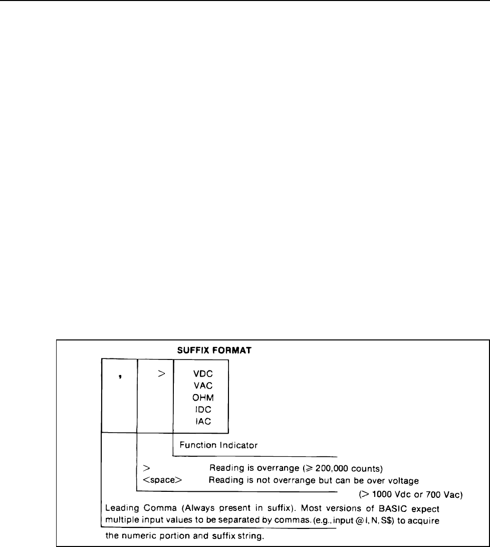
8842A
Instruction Manual
3-10
3-10. Fn (Function Commands)
The function commands duplicate the front panel function buttons. The 8842A defaults to
F1 on power-up and on any device-clear command (*, DCL, or SDC). If F0 is sent to the
8842A, it is internally converted to F1. The function setting can be read using the G0
command.
As with the front panel commands, selecting F6 automatically selects the 2000 mA range
(R5). If the instrument is in range R8, commanding F5 automatically selects the 200 mA
range (R4). If the instrument is in R1 through R6, commanding F5 automatically selects
the 2000 mA range (R5). If the 8842A is in a resistance function (F3 or F4) and in R6,
selecting any other function automatically selects R5. If the 8842A is in range R8 and F2
or F3 is commanded, range R1 is selected.
Example Explanation
"F3" Selects 2 WIRE kΩ function; it does not affect any other settings.
"* F6" Selects mA AC function and 2000 mA range. Resets all other settings to
default.
3-11. Get Commands
The Get commands "get" information from the 8842A for the controller. Each Get
command loads the output buffer with an output string in the format shown in Figure 3-6.
Status data (the output from Get commands G0, G1, G3, G4, G5, G6, G7 and G8) is
interpreted as shown in Table 3-1. The Get commands should not be confused with the
interface message GET (Group Execute Trigger).
f3-06.wmf
Figure 3-6. Output Data Format

Remote Programming
DEVICE-DEPENDENT COMMAND SET
3
3-11
Table 3-1. Status Data
COMMAND
OUTPUT
STRING MEANING
G0 Frst F = 1 – 6 as in Funtion commands (Fn)
9 for Self-Test
r = 1 – 6 and 8 in Range commands (Rn)
s = 0 – 2 as in Reading Rate commands (Sn)
t = 0 – 4 as in Trigger Mode commands (Tn)
G1 nn nn = 00 for SRQ disabled (default)
01 for SRQ on overrange
04 for SRQ on front panel SRQ
08 for SRQ on cal step complete
16 for SRQ on data availible
32 for SRQ on any error
Note: SRQ mask values may be added for combinations.Example:
33 for SRQ on overrange or any error.
G3 aaaaaaaaaaaaaaaa 16 user-defined ASCII characters
G4 10vm V = 0 Not in cal verification
1 Cal verification
m = 0 Not in calibration mode
1 A/D calibration
2 Offset and gain calibration
4 HF AC calibration
G5 1iab I = 0 FRONT inputs selected
1 REAR inputs selected
a = 0Autorange on
1 Autorange off (manual range)
b = 0 OFFSET off
1 OFFSET on
G6 10yw Y = 0 output suffix disabled
1 output suffix enabled
w = 0 – 7 as in Terminator commands (Wn)
G7 10nn nn represents error code (See Table 2-1)
G8 FLUKE,
mmmmm,
0, Vn.n
Mmmmm = 8842A
Vn.n = IEEE-488 Interface software version number
The output data from some Get commands starts with a leading 1 or 10. This prevents the
controller from suppressing leading zeroes and gives a uniform four-character length to
all instrument configuration data (the data from Get commands G0, G4, G5, G6, and G7).
The Get commands are described further in the following paragraphs. For more
information about output data, see paragraph 3-39.

8842A
Instruction Manual
3-12
3-12. G0 (Get Instrument Configuration)
The G0 command copies the 8842A function, range, reading rate, and trigger mode into
the output buffer in the format shown in Figure 3-6. The four digits returned represent the
arguments for the equivalent F, R, S, and T commands, as shown in Table 3-1. An
example output string follows.
Example Explanation
3410 CR LF 3: F3 (2 WIRE kΩ function)
4: R4 (200 kΩ range)
1: S1 (Medium reading rate)
0: T0 (Continuous trigger)
The second digit, which can vary from 1 to 6, indicates what measurement range the
8842A is in regardless of whether the 8842A is in autorange or manual range.
The output string from a G0 command is acceptable as an argument for an "N" command.
This allows you to configure the 8842A from the front panel and then record the
configuration over the bus for future use with a P0 command. However, 9mmm (meaning
self-test) can not be used with the P0 command.
3-13. G1 (Get SRQ Mask)
The G1 command copies the present SRQ mask into the output buffer in the format
shown in Figure 3-6. The SRQ mask values are explained in Table 3-1. An example
output string follows. For more about the SRQ mask, see paragraph 3-47.
Example Explanation
33 CR LF Enable SRQ on any error or overrange
3-14. G2 (Get Calibration Prompt)
The G2 command is used when calibrating the 8842A under remote control. The
command loads the output buffer with a calibration prompt that represents the input
expected at the analog inputs. The calibration prompt is formatted as a signed decimal
with exponent, as shown in Figure 3-6. The suffix may be enabled with the Y1 command.
Example output strings follow.
Examples Explanation
+1.00000E+0 CR LF Calibration prompt
+190.000E-3 CR LF Calibration prompt
+1.90000E+0, VDC CR LF Calibration prompt (Suffix enabled)
If an error has occurred, the G2 command loads the output buffer with an error message
instead of the prompt. (See paragraph 3-39.)
The G2 command is valid only when the calibration mode is enabled by pressing the
front panel CAL ENABLE switch. If the 8842A is not in the calibration mode, the G2
command generates an error message.

Remote Programming
DEVICE-DEPENDENT COMMAND SET
3
3-13
3-15. G3 (Get User-Defined Message)
The G3 command loads the output buffer with the user-defined message stored in
calibration memory during the calibration procedure. The message consists of 16 ASCII
characters, as shown in Figure 3-6.
The message is stored in calibration memory during calibration using the P3 command. If
fewer than 16 characters have been stored, the remaining characters returned are spaces.
If no message has ever been stored, a string of 16 null characters (hex 00) will be
returned. Some example output strings follow.
Example Explanation
FL8842A.12-17-83 CR LF Identifies instrument and gives cal date.
01-25-84 CR LF Gives cal date. The last eight characters are
blank.
3-16. G4 (Get Calibration Status)
The G4 command is used when calibrating the 8842A under remote control. The
command loads the output buffer with the instrument’s calibration status in the format
shown in Figure 3-6. The status is represented by a four-digit integer which is interpreted
in Table 3-1.
The first two digits are always 1 and 0. The third digit indicates whether or not the
calibration verification mode is enabled. (This mode is enabled only when the calibration
mode is enabled.) The fourth digit indicates whether or not the calibration mode is
enabled, and if so, which part of the calibration procedure the 8842A is in. Example
output strings follow.
Example Explanation
1000 CR LF 1: Leading 1
0: Leading 0
0: Not in cal verification
0: Cal mode disabled
1001 CR LF 1: Leading 1
0: Leading 0
0: Not in cal verification
1: Cal mode enabled; A/D cal selected

8842A
Instruction Manual
3-14
3-17. G5 (Get IAB Status)
The G5 command loads the output buffer with the IAB status in the format shown in
Figure 3-6. As Table 3-1 explains, the IAB status is a four-character string which
indicates the status of the FRONT/REAR switch (front or rear analog inputs selected), the
autorange feature (autorange on or off), and the OFFSET feature (OFFSET on or off).
The first digit is always 1. An example output string follows.
Example Explanation
1011 CR LF 1: Leading 1
0: FRONT inputs
1: Autorange off
1: OFFSET feature on
It is useful to know whether autorange is on or off because this information is not
available from the G0 command. For example, the G0 command could indicate that the
8842A was in the 200 mV range, but it would not indicate whether the 8842A was in
autorange or manual range.
3-18. G6 (Get YW Status)
The G6 command loads the output buffer with the YW status in the format shown in
Figure 3-6. The YW status is a four-character string which indicates which terminators
are selected and whether the output suffix is enabled or disabled, as shown in Table 3-1.
The first two digits are always 1 and 0. An example output string follows.
Example Explanation
1015 LF CR 1: Leading 1
0: Leading 0
1: Y1 (enable output suffix)
5: W5 (enable LF only)
3-19. G7 (Get Error Status)
The G7 command copies the error status register into the output buffer in the format
shown in Figure 3-6. The first two digits are always 1 and 0. The second two digits
represent the appropriate error code, if an error has occurred. (Error codes are listed in
Table 2-1, Section 2). If an error has not occurred, the second two digits are 00. An
example output string follows.
Example Explanation
1071 CR LF 1: Leading 1
0: Leading 0
71: Syntax error in device-dependent command string
The G7 command gives the error status as it exists when the command is executed at its
position in the input string. The G7 command does not clear the error status register. For
more information about error messages, see paragraph 3-40.

Remote Programming
DEVICE-DEPENDENT COMMAND SET
3
3-15
3-20. G8 (Get Instrument Identification)
The G8 command copies the 8842A instrument identification into the output buffer in the
format shown in Figure 3-6. The identification is represented by four comma separated
fields that are interpreted in Table 3-1.
The first field indicates the manufacturer, the second indicates the instrument model
number, the third is always zero, and the fourth indicates the version number of the
IEEE-488 interface software.
Example Explanation
FLUKE,8842A,0,V4.0 CR LF This instrument is a Fluke 8842A with IEEE-
488 interface software version 4.0.
3-21. N (Numeric Entry Command)
Format Explanation
N<numeric entry> Where <numeric entry> is one of the following:
<signed integer>
<signed real number without exponent>
<signed real number>E<signed exponent>
Example Explanation
"N12001" Enters the five-digit integer 12001
"N-1.23E2" Enters -1.23 x 10²
"N+154.33E-1" Enters 1.5433 x 101
The N command enters numeric values for use with subsequent Put commands. The
interpretation of the numeric value depends on which Put command it is used with.
The E can be used within an N command for entering an exponent of 10. The N can be
used without an E, but an E requires a prior N. The exponent can be any integer from -9
to +9.
The mantissa may exceed 5-1/2 digits. The 8842A accurately calculates the appropriate
exponent and then disregards all but the first 5-1/2 digits of the mantissa. However, a
syntax error will occur if the numeric entry overflows the input buffer.
Example Explanation
"N123456789" Enters +1.23456 x 10⁸
3-22. Put Commands
The Put commands P0 through P3 set up the 8842A’s configuration and operating modes
by entering ("putting") information in the appropriate registers. The put commands are
described further in the following paragraphs.
3-23. P0 (Put Instrument Configuration)
Format Explanation
N<frst>P0 Where <frst> is a four-digit integer interpreted as arguments for the F,
R, S, and T commands.
Example Explanation

8842A
Instruction Manual
3-16
"N3120 P0" Identical to F3 R1 S2 T0. Selects 2 WIRE kΩ function, 200Ω range,
fast sample rate, continuous trigger.
The P0 command allows broadside loading of the Function, Range, Reading Rate, and
Trigger Mode commands (F, R, S, and T). The codes for these commands are listed in
Figure 3-5.
A numeric entry for P0 must be within +1000 and +6824. Each of the four digits must not
exceed its maximum allowed value (6, 8, 2, and 4, respectively) or an error message will
occur and the instrument configuration will remain unchanged. The entry may be
expressed as an integer, real number, or real number with exponent, as described under
the N command. Any fractional part is ignored.
Example Explanation
"N3112 P0" Sets the 8842A to F3, R1, S1, and T2.
3-24. P1 (Put SRQ Mask)
Format Explanation
N<SRQ mask>P1 Where <SRQ mask> is a two-digit integer from 00 to 63.
The P1 command is used to program the 8842A to make service requests on user-
specified conditions. The two-digit code for the SRQ mask is interpreted in Table 3-1
under the G1 command. For more about the SRQ mask, see paragraph 3-51.
Numeric entries for the P1 command must be between 0 and +63 (inclusive), or an error
will occur and the SRQ mask will remain unchanged. The entry may be expressed as an
integer, real number, or real number with exponent, as described under the N command.
Any fractional part is ignored.
Example Explanation
"N0.17E+2 P1" Sets SRQ mask to 17. Enables SRQ on data available or overrange.
"N1 P1" Sets SRQ mask to 01. (A leading zero is assumed.) Enables SRQ on
overrange.
3-25. P2 (Put Calibration Value)
Format Explanation
N<value>P2 Where <value> can be an integer, real number, or real number with
exponent, as described under the N command.
Example Explanation
"N1 P2" If the 8842A is in VDC, the next calibration input expected is
1.00000V dc.
The P2 command is used to enter variable input calibration values just like the front panel
VAR IN button. To accept the P2 command, the 8842A must be in the calibration mode
(enabled by pressing the front panel CAL ENABLE switch). Otherwise, the P2 command
will generate an error message.
The variable input is a measurement value that is to be used as the calibration value for
the next calibration step. Its format is the same as a measurement value. But since it is
coming from the controller, the value can be specified using any valid format (signed
interger, real number, or real number with exponent). For example, if the 8842A prompts
for an input value of 100Ω for the next calibration step, but the available source is
98.97Ω, the variable input can be specified as "N+9.897E+1", "N0.9897E2", N9897E-2",

Remote Programming
DEVICE-DEPENDENT COMMAND SET
3
3-17
etc. All of these strings result in the same value being used for the next calibration step.
For complete information about remote calibration, refer to the Maintenance section.
Numeric values exceeding full scale and negative values for ohms and AC generate error
messages.
3-26. P3 (Put User-Defined Message)
Format Explanation
P3<value> Where <value> is a string of up to 16 ASCII characters.
Example Explanation
"P3FL.8842.12-17-83" Loads the message "FL.8842.12-17-83" into calibration
memory.
"P3HIMOM" Loads the message "HIMOM" into calibration memory. The
remaining eleven characters are assumed to be blank.
The P3 command stores a user-defined message in the internal calibration memory during
remote calibration. The message may be read with a subsequent G3 command.
The message may consist of up to 16 ASCII characters, and typically represents the
instrument’s identification, calibration date, calibration facility, etc. If fewer than 16
characters are specified, spaces are appended to fill the message to 16 characters. Spaces
and commas in the 16-character input string are suppressed. Lower-case letters are
converted to upper-case.
NOTE
If fewer than 16 characters are specified, the P3 command must not be
followed by other commands in the same input command string. Otherwise,
the subsequent commands will be misinterpreted as part of the 16-character
string.
To accept the P3 command, the 8842A must be in the calibration mode (enabled by
pressing the front panel CAL ENABLE switch). Otherwise, the P3 command will
generate an error message.
3-27. Rn (Range Commands)
The Range commands duplicate the front panel range buttons. For example, R0 selects
autorange, and R3 selects the 20V/20 kQ range.
The R7 command turns autorange off, just as the AUTO button does when it is toggled.
Command R7 puts the 8842A into manual range, selecting whatever range the instrument
is in when the command is received.
The 8842A defaults to R0 on power-up and any device-clear command (*, DCL, or
SDC). The range setting can be read using the G0 command.
3-28. Sn (Reading Rate Commands)
The Reading Rate commands duplicate the front panel RATE button. Like the RATE
button, the reading rate command also selects the number of digits displayed and the
filter setting. (Filter settings are shown in the specifications in Section 1).
The 8842A defaults to S0 on power-up and any device-clear command (*, DCL, or
SDC). The reading rate can be read using the G0 command.
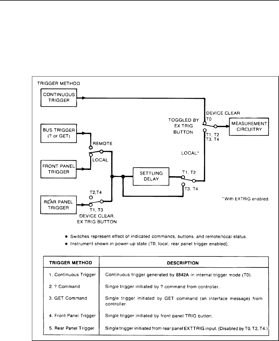
8842A
Instruction Manual
3-18
3-29. Tn (Trigger Mode Commands)
The Trigger Mode commands duplicate the front panel EX TRIG button. In addition, the
commands can enable or disable the rear panel trigger and the automatic settling time
delay.
Figure 3-7 illustrates how to select among the five types of triggers: continuous trigger,
front panel trigger, rear panel trigger, and two bus triggers. Note that the front panel
TRIG button is enabled only while the instrument is under local control.
f3-07.wmf
Figure 3-6. Trigger Selection Logic Diagram
In the continuous trigger mode (T0), triggers are initiated at the selected reading rate.
Each new reading is loaded into the output buffer as it becomes available, unless the
instrument is busy sending previous output data.

Remote Programming
DEVICE-DEPENDENT COMMAND SET
3
3-19
The trigger mode can be read using the G0 command. The 8842A defaults to T0 on both
power-up and any device-clear command (*, DCL, or SDC).
3-30. Wn (Terminator Commands)
The Terminator commands select what terminators the 8842A appends to every output
string. The available terminators are: Carriage Return (CR), Line Feed (LF), and End Or
Identify (EOI).
CR and LF are ASCII control codes, sent over the data lines just like output data. EOI is a
uniline message which is sent simultaneously with the last character in the output string.
Normally, each output string is terminated with CR followed by LF and EOI.
The terminator selection can be read using the G6 command. The 8842A defaults to W0
on power-up and any device-clear command.
3-31. X0 (Clear Error Register Command)
The X0 command clears the 8842A’s error status register. After an X0 command is
executed, a G7 command (Get Error Status) would return 1000 (no errors).
Note that the error status register is also cleared when any device-clear command (*,
DCL, or SDC) is executed. However, X0 is useful for clearing the error status register
without forcing a complete instrument clear (as do the device-clear commands).
3-32. Yn (Suffix Commands)
The Suffix commands enable or disable a suffix which the 8842A can append to all
numeric data (the data in response to G2 or trigger commands). The suffix includes a
comma, an overrange indicator (>), and a function indicator (VDC, VAC, OHM, IDC, or
IAC). The suffix is illustrated in Figure 3-6. An example of suffixed data is given in
paragraph 3-43.
To read suffixed data with a controller using BASIC, one can read the whole line into a
string variable and then convert the numeric part into a numeric variable. However, it is
much easier to read the numeric part directly into a numeric variable and the suffix into a
string variable. The leading comma of the suffix serves as a convenient delimiter. For
example, a BASIC program statement might be:
INPUT @1,A, B$
The suffix status can be read using the G6 command. The 8842A defaults to Y0 on
power-up and any device-clear command (*, DCL or SDC), unless in talk-only mode.
3-33. Z0 (Self-Test Command)
The Z0 command initiates the diagnostic self-tests as does pressing the front panel SRQ
button for 3 seconds. The 8842A then runs through the tests in sequence. (For a
description of the self-tests, see the Maintenance section.)
If the 8842A detects an error, an error message is loaded into the output buffer and
displayed on the front panel. After the last test, the 8842A is reset to the power-up
configuration, and it begins taking readings.
It is an error to send the 8842A device-dependent commands during the self-tests.
However, the controller can still make the 8842A a talker to read the output buffer during
the test, and thus record each error that occurs, except that only the last of the digital self-
test errors can be read. After the tests, only the last error is stored in the output buffer if
more than one error occurred.

8842A
Instruction Manual
3-20
Error messages are indicated by an exponent of +21. For more about error messages, see
paragraph 3-40.
Since the 8842A is reset at the end of the self-tests, the Z0 command should be the last
command in a given command string. The 8842A will ignore any subsequent commands
in the same command string.
When the self-tests are complete and no errors have occurred, the serial poll register will
have bit 5 (Data Available) true and bit 6 (Any Error) false. See paragraph 3-50 for more
about the serial poll register.
3-34. (Device-Clear Command)
The asterisk command (*) is a device-dependent message which resets the 8842A to the
power-up default settings and clears all registers and buffers except for the input buffer.
The remote/local status remains unchanged. The asterisk command performs the
following:
1. Implements the default settings F1, R0, S0, T0, D0, B0, Y0, W0.
2. Clears the error status register (equivalent to X0).
3. Zeros the SRQ mask, prohibiting service requests (equivalent to N0 P1).
4. Zeros the numeric entry register (equivalent to N0).
5. Zeros the serial poll register.
6. Sets the SRQ line false.
The asterisk command is executed in its proper turn in a string, just like any other
command, without affecting the contents of the input buffer. All commands which
precede the asterisk command are performed.
The asterisk command is useful to ensure that the 8842A is initialized to the same state
each time a program is run. By contrast, the similar interface messages DCL (Device
Clear) and SDC (Selected Device Clear) cause the entire input buffer to be cleared
immediately.
DCL, SDC, and the asterisk command are all considered to be device-clear commands
because the results are so similar; however, DCL and SDC are not identical to the asterisk
command described here. DCL and SDC are discussed further in the paragraph on
interface messages.
3-35. ? (Single-Trigger Command)
The Single-Trigger command (?) causes the 8842A to take a reading and place the result
into the output buffer. To accept this command, the 8842A must be in external trigger
mode (selected by the T1, T2, T3, or T4 command).
The Single-Trigger command is one of five ways to trigger a reading. (See Figure 3-7.)
Of these, only the Single-Trigger command (?) and the Group Execute Trigger command
(GET) are loaded into the input buffer.
3-36. INPUT SYNTAX
The following paragraphs describe how to construct groups of commands for the 8842A.
A few definitions are presented first, followed by a description of how the 8842A
processes input commands. Guidelines are then summarized in four syntax rules.

Remote Programming
INPUT SYNTAX
3
3-21
3-37. Definitions
• Output commands: Commands which load data into the output buffer. The output
commands are: the Get commands (G0 through G8); the Single-Trigger Command
(?); the Continuous Trigger command (T0); and Group Execute Trigger (GET), not to
be confused with the Get commands.
• Input terminator: An ASCII control code sent by the controller which tells the 8842A
to execute all device-dependent commands since the previous terminator.
Terminators are CR (Carriage Return), LF (Line Feed), EOI (End Or Identify), and
GET (Group Execute Trigger).
• Input command string: One or more device-dependent commands followed by a
terminator.
3-38. Input Processing
When the 8842A receives commands from the bus, it stores them in a 31-character input
buffer as a continuous string of characters. Commands in the input buffer are not
executed or checked for syntax until an input terminator is received or the input buffer
becomes full. The only valid input terminators are CR, LF, GET (Group Execute
Trigger), and/or EOI.
When the 8842A receives an input terminator, it executes the previous commands in the
order in which they were received. As input characters are processed and executed, space
is made available in the input buffer for new characters.
If the input buffer becomes full, the 8842A stops accepting characters from the bus until
all complete command strings currently in the input buffer have been executed. In this
way, characters sent to the 8842A are never lost due to buffer overflow.
In some instances, a terminator is automatically transmitted at the end of the controller’s
output string. For example, in Fluke BASIC, the PRINT statement always finishes with a
CR LF pair. If a controller does not have this feature, the programmer must transmit a
terminator explicitly.
The 8842A accepts alphabetic characters in either upper or lower case. Spaces, commas,
and control codes are ignored and are not placed in the input buffer. If the 8842A
receives a group of terminators (such as CR LF or CR LF EOI), only a single terminator
is loaded into the input buffer. Numeric values used in PUT commands may be in NR1,
NR2, or NR3 format as described in the IEEE-488 Codes and Formats Recommended
Practice. (These correspond to the signed integer, real number, and real-number-with-
exponent formats described under the N command.) For reference, Figure 3-8 shows how
the 8842A interprets messages.

8842A
Instruction Manual
3-22
DEVICE-DEPENDENT MESSAGES
Single-character Commands
Bn Cn Dn Fn Gn Pn Rn Sn Wn Xn Yn Zn Each of these commands requires the single
numeric digit (n).
Numeric-entry Characters
NE. + - 0123456789 These characters are used for entering numbers
Terminators
CR Carriage Return
LF Line Feed
GET Group Execute Trigger
EOI End Or Idenity (used as END/DAB)
INTERFACE MESSAGES
Address Messages
MLA My Listen Address
MTA My Talk address
UNL Unlisten
UNT Untalk
Universal Commands
ATN Attention
DCL Device Clear
IFC Interface Clear
LLO Local Lockout
REN Remote Enable
SPD Serial Poll Disable
SPE Serial Poll Enable
Addressed Commands
GET Group Execute Trigger
GTL Go to Local
SDC Selected Device Clear
Ignored Characters
, comma These characters may be inserted anywhere in a
character string without affecting the string.
Space Character string without affecting the string.
All Other ASCII non-printing characters (except CR
and LF) They carry no special meaning and are ignored by
the 8842A. They are not placed in the input buffer.
ERROR-PRODUCING CHARACTERS
! “ # $ ‘ ( ) / : < = > ; @ [ / ] ~
HIJKLMOQUV
The error annunciator is displayed on the 8842A
front panel when one of these characters is
encountered (ERROR 71).
Figure 3-7. Interpretation of Messages

Remote Programming
INPUT SYNTAX
3
3-23
Illegal commands (e.g., F9) generate an error message, but are otherwise ignored, and do
not affect the instrument’s configuration.
Example Explanation
"* F9" This would load the output buffer with an error message and select F1
(established by the * command).
3-39. Syntax Rules
Four syntax rules should be followed when constructing input command strings. They
are:
• RULE 1: Read output data only once.
To prevent old (previously read) data from being read a second time by mistake, the
output buffer is always cleared after it has been read. If the output buffer is read twice
without an intervening output command, the 8842A will not respond to the second
attempt to read the output buffer. (However, if the 8842A is in T0, no intervening
command is necessary.)
• RULE 2: Use no more than one output command per input command string.
Because the 8842A has only one output buffer, it writes new data over old. If an input
command string contains more than one output command, only the data from the last
command can be read.
Example Explanation
"F1 T3 ? F2 ?" Improper construction. The second trigger writes over the first. To
obtain two readings, send two complete command strings (separated by
terminators).
"F2 R3 S0 T3 ?" Correct construction. The string contains only one output command.
"F2 R3 S0" Correct construction. It is permissible for a string not to contain an
output command.
• RULE 3: Read the output data generated by one input command string before sending
the next input command string.
Output data remains available in the output buffer until it is read, or until the next
input command string is received. As soon as the controller finishes reading the output
buffer, or as soon as the 8842A receives a new input terminator, the Data Available bit
in the serial poll register is set false. When this bit is false, data can no longer be read
from the output buffer. Therefore, an output string which is available must be read by
the controller before, rather than after, the next input command string is sent.
Rule 3 is most evident in the external trigger mode, and is best demonstrated by a
programming example. The following program is written first incorrectly, and then
correctly, in Fluke BASIC using the 1722A Instrument Controller.
Incorrect example
100 PRINT @3, "T1 ?"
200 PRINT @3, "F4"
300 INPUT @3, A

8842A
Instruction Manual
3-24
In this incorrect example, the INPUT statement is located incorrectly for reading the
measurement data from line 100. The new input command string "F4" disallows the
reading of data from the output buffer.
Correct example
100 PRINT @3, "T1 ?"
200 INPUT @3, A
300 PRINT @3, "F4"
In this example, the reading taken at line 100 is read at line 200. Then the F4 command is
sent. Note that in the external trigger mode, the reading from line 100 flashes on the
8842A display too briefly to see. This is because the function change at line 300 blanks
the display until the next trigger.
The previous example could also be correctly programmed as follows:
100 PRINT @3, "T1 ? F4"
200 INPUT @3, A
• RULE 4: If an input command string contains a trigger, enter the commands in the
following order:
a. Commands to configure the instrument (if any).
b. The trigger command.
c. Commands to re-configure the instrument (if any).
d. Terminator(s).
The principle behind this rule is that the 8842A executes all commands in the exact order
they are received, from left to right as written.
Example Explanation
"F3 F4 ?" Improper construction. F3 is effectively discarded.
"F3 ? F4" Correct construction. The 8842A is configured in F3, and the trigger is
executed. Then the 8842A is left in F4.
3-40. OUTPUT DATA
The following paragraphs describe the data that can be loaded into the 8842A output
buffer and sent to the IEEE-488 bus. The paragraphs describe how and when data is
loaded into the output buffer, the types of output data, and their relative priority.
Note that the 8842A can also send data to the IEEE-488 bus from the serial poll register.
For a description of this data, see paragraph 3-47.
3-41. Loading Output Data
The output buffer is loaded when the 8842A receives an output command, or when an
error occurs. Output commands are those device-dependent commands which load the
output buffer with data:
• Get commands (G0 through G8)
• Single-trigger command (?)
• Group execute trigger (GET)
• Continuous Trigger (T0)
Remote Programming
OUTPUT DATA
3
3-25
Because the 8842A gives priority to input processing, it completely processes all
characters in the input buffer before it loads the output buffer. When the output buffer is
loaded, the Data Available bit in the serial poll register is set true.
Data from the output buffer is not actually loaded onto the IEEE-488 bus until the
controller addresses the 8842A as a talker. This is done by sending the interface message
MTA (My Talk Address).
3-42. Types of Output Data
The types of data that can be loaded into the output buffer are shown in Figure 3-6. Each
type has its own format. Error messages, which are loaded into the output buffer if an
error occurs, are formatted as numeric data.
3-43. Numeric Data and Error Messages
Numeric data is loaded into the output buffer in response to the G2 command or an
instrument trigger, and has the format shown in Table 3-2. The exponent is always a
multiple of 3, as in engineering notation. The position of the decimal point matches the
front panel display.
Numeric data is of constant length, It is 11 characters (plus terminators) when the suffix
is disabled, and 16 characters (plus terminators) when the suffix is enabled.
The suffix is enabled by the Y1 command, and consists of five ASCII characters as
shown in Figure 3-6. The suffix is appended only to numeric data, never to status data.
The terminators are determined by the Terminator commands. The default is CR LF EOI.
There are three types of numeric data: measurement data, overrange indication, and error
messages.
3-44. MEASUREMENT DATA
Measurement data has the numeric data format shown in Table 3-2, and is always in the
units of volts, amps, or ohms.
Table 3-2. Numeric Output Data Format
MEASUREMENT DATA
RANGE
VDC, VAC 2-, 4-WIRE kΩMA DC, mA AC
OVERRANGE
INDICATION
ERROR
MESSAGES
R8 ±1x.xxxxE-3* ±1x.xxxxE+0** -- ±9.99999E+9 +1.00xxE+21
R1 ±1xx.xxxE-3 ±1xx.xxxE+0 -- ±9.99999E+9 +1.00xxE+21
R2 ±1.xxxxxE+0 ±1.xxxxxE+3 -- ±9.99999E+9 +1.00xxE+21
R3 ±1x.xxxxE+0 ±1x.xxxxE+3 -- ±9.99999E+9 +1.00xxE+21
R4 ±1xx.xxxE+0 ±1xx.xxxE+3 ±1xx.xxxE-3*** ±9.99999E+9 +1.00xxE+21
R5 ±1xxx.xxE+0 ±1xxx.xxE+3 ±1xxx.xxE-3 ±9.99999E+9 +1.00xxE+21
R6 -- ±1x.xxxxE+6 -- ±9.99999E+9 +1.00xxE+21
* VDC only
** 4-wire ohms
*** mA DC only

8842A
Instruction Manual
3-26
NOTE
In the fast (F) reading rate, the least significant digit is always zero, and
should be disregarded when interpreting accuracy specifications.
3-45. OVERRANGE INDICATION
If a reading is overrange (≥ 200,000 counts), the measurement data has the following
format:
±9.99999E+9 <suffix> <terminators>
Overvoltage readings (> 1000V dc or 700V ac) do not result in this display.
3-46. ERROR MESSAGES
If the 8842A detects an error, it loads an error message into the output buffer in the
following numeric format:
+1.00xxE+21 <terminators>
The digits xx represent a two-digit error code. (Error codes are listed in Table 2-1,
Section 2.) The suffix is always suppressed for error messages.
Example Explanation
+1.0071E+21 CR LF ERROR 71: Syntax error in device-dependent command string.
As with local operation, none of the errors are latching except for ERROR 31. If the mA
DC or mA AC function is requested while the FRONT/REAR switch is in the REAR
position, ERROR 31 will persist until the switch is set to FRONT or another function is
selected.
To check for an error condition, test whether the output buffer data is greater than or
equal to +1E+21, or test the Any Error bit (bit 6) in the serial poll register.
3-47. Status Data
Status data is the output in response to G0, G1, G3, G4, G5, G6, G7 and G8, commands.
The data is formatted as shown in Figure 3-2, and is interpreted in Table 3-1. Examples
of status data can be found in the description of the Get commands.
The user-defined message loaded by the G3 command consists of 16 characters plus
terminators. The SRQ mask loaded by the G1 command consists of two integers plus
terminators. All other status data is always a four-digit integer plus terminators. The
terminators LF (Line Feed) and CR (Carriage Return) each add an extra character when
enabled.
The 8842A begins some status data with a leading ASCII one (1) or a one and a zero
(10). This prevents the controller from suppressing any leading zeros present in the
8842A’s output string. It also gives a uniform four-character length to all instrument
configuration data.
Status data from the Get commands reflects the status of the 8842A at the time the
command is executed at its place in the input command string.
3-48. Output Priority
Since only one output string is allowed per input command string, the 8842A gives
priority to some types of data over others. An input command string may call for more
than one output string. (For example, an input string may contain a Get command but
also cause an error message.) However, the output buffer is loaded with only one output
string. That string is selected according to the following priority:

Remote Programming
SERVICE REQUESTS
3
3-27
1. Status data (from G0, G1, G3, G4, G5, G6, G7 and G8)
2. Error messages (if an error exists)
3. Numeric data (from G2 or a trigger)
This means that an error message always overrides numeric data, but status data is sent
even in the presence of an error. However, the status data does not clear the error
message; the error message is sent the next time numeric data is requested.
3-49. SERVICE REQUESTS
Service requests let bus instruments get the attention of the system controller. The
requests are sent over the SRQ line (one of the IEEE-488 bus lines). If more than one
instrument on the bus is capable of sending service requests, the controller can learn
which one made the request by taking a serial poll. Each device (including the 8842A)
responds to the poll by sending the contents of its serial poll register. The serial poll
register indicates whether or not the device requested service, and if so, the reason for the
request.
The 8842A may be programmed to make a service request on user-specified conditions.
The conditions are specified by entering a value for the service request mask (SRQ mask)
with the P1 command. The SRQ mask works by monitoring the serial poll register, which
in turn monitors various conditions in the 8842A.
3-50. The Serial Poll Register
The serial poll register is a binary-encoded register which contains eight bits, as
illustrated in Figure 3-9. The controller can read the 8842A serial poll register at any time
by taking a serial poll. Because serial poll register data is loaded directly onto the bus
(instead of being loaded into the output buffer first), reading the serial poll register leaves
data in the output buffer intact.
Service requests may also be initiated using the front panel SRQ button if it has been
enabled by the SRQ mask.
The eight bits of the serial poll register are described in Figure 3-9. Note that the SRQ
mask uses bits 1 through 6 to set bit 7 (the RQS bit). When the RQS bit is set true, the
8842A sets the SRQ line true, which generates a service request. A bit is considered true
when it is set to 1.
8842A
Instruction Manual
3-28
BIT: 8 7 6 5 4 3 2 1
0 RQS ANY
ERROR
DATA
AVAILIBLE
CAL STEP
COMPLETE
FRONT
PANEL SRQ
0 OVER-
RANGE
DECIMAL
VALUE:
64 32 16 8 4 2 1
Bit Name Set Cleared
1 Overrange An overrange condition occurs Device command received, or
Bus or Rear Panel Trigger, or
Output buffer is read
2 Not used Never Always
3 Front panel SRQ Front panel SRQ button
pressed
Device command received
4 Cal Step Complete Completion of store command
(C0)
Device command received
5 Data Availible Output buffer loaded with any
data (Readings, Error
Messages. Get Responses)
Device command received, or
Bus or Rear Panel Trigger, or
Output buffer is read
6 Any Error An error condition occurs. At
the same time the output buffer
is loaded with an error
message. This sets bit 5.
Device command received, or
Output buffer is read
7 RQS Any SRQ mask-enabled bit is
set.
All SRQ mask-enabled bits are
cleared
8 Not used Never Always
Figure 3-8. Serial Poll Register
For example, the serial poll register reads 00010000 (binary) when data is available. This
value is read in binary by the controller, which might numerically reformat the value to
16 (decimal) or 10 (hexadecimal).
The serial poll register is cleared whenever the 8842A receives a new input command
string.
3-51. The SRQ Mask
The SRQ mask is a two-digit integer that specifies which conditions will generate a
service request. The SRQ mask is entered using the P1 command and can be read with
the G1 command. The conditions corresponding to each SRQ mask value are listed under
G1 in Table 3-1.

Remote Programming
INTERFACE MESSAGES
3
3-29
The SRQ mask can enable any combination of serial poll register bits 1 through 6. Its six-
bit binary representation is ANDed bit-for-bit with serial poll register bits 1 through 6
whenever the output buffer is loaded. If any mask-enabled bit in the serial poll register
comes true, the RQS bit (bit 7) is set true, generating a service request.
Example Explanation
"* N4 P1 ?" An SRQ is generated if the front panel SRQ button is pressed. The string
sets the SRQ mask to 04, which is 000100 in binary. This mask is ANDed
with the lower six bits of the serial poll register. The mask thus enables bit
3, the Front Panel SRQ bit.
The SRQ mask codes can be added to select combinations of conditions.
Example Explanation
"* N5 P1 ?" An SRQ is generated if the SRQ button is pressed or if the trigger results
in an overrange reading. The SRQ mask is set to 05, which is 000101 in
binary.
At power-up or on any device-clear command, the SRQ mask is set to 00 (decimal). This
prevents service requests by holding the RQS bit false under all conditions. For other
examples of the SRQ mask, see the description of the P1 command.
3-52. INTERFACE MESSAGES
The interface messages understood by the 8842A can be separated into the three main
classes described in the IEEE-488 Standard: address messages (AD), universal
commands (UC), and addressed commands (AC). All interface messages described here
originate at the controller.
3-53. Address Messages
Address messages are used by the controller to communicate talk and listen control to
other devices on the bus. Address messages are sent over the eight data lines of the bus
while the controller holds ATN true. Address messages are processed immediately and
are not placed in the input buffer. The address messages are:
• MLA My Listen Address -- Addresses a device to listen
• MTA My Talk Address -- Addresses a device to talk
• UNL Unlisten -- Addresses all listeners to unlisten
• UNT Untalk -- Addresses all talkers to untalk
3-54. Universal Commands
Universal commands are accepted and interpreted by all devices on the bus. The
commands are of two types, multiline messages and uniline messages. Multiline
messages are sent over the eight parallel data lines in the IEEE-488 bus. Uniline
messages are sent over one of the individual interface management lines in the IEEE-488
bus. All universal commands except DCL are processed immediately by the 8842A,
ahead of any device-dependent commands. Only DCL enters the 8842A input buffer.
The 8842A responds to the following universal messages:
ATN Attention -- A uniline message which causes the 8842A to interpret multiline
messages as interface messages (AD, AC, or UC). When false, multiline
messages are interpreted as device-dependent messages.

8842A
Instruction Manual
3-30
IFC Interface Clear -- A uniline message which clears only the interface (not the
8842A) by placing it in a known quiescent state.
REN Remote Enable -- A uniline message which, when received with MLA, switches
the 8842A to remote. When REN is set false, the 8842A switches to local and
removes local lockout.
DCL Device Clear -- A multiline message which is loaded into the input buffer as a
special device-clear command. DCL performs the same operation as the device-
dependent command *, except that it is read before any other characters that are
already present in the input buffer, and clears the entire input buffer. Processing
then continues normally. The action of DCL is not immediate; if the 8842A is
taking a reading when DCL is received, the DCL command is executed after the
measurement is finished.
LLO Local Lockout -- A multiline message which disables the front panel LOCAL
button. The result is that the local mode is not accessible by front panel control.
SPD Serial Poll Disable -- A multiline message which removes the serial poll enable
state.
SPE Serial Poll Enable -- A multiline message which causes the serial poll data (rather
than output buffer data) to be transferred on the bus once ATN becomes false.
3-55. Addressed Commands
Addressed commands are multiline messages which are accepted and interpreted by only
those devices currently addressed to listen. The 8842A responds to the following
addressed commands:
GET Group Execute Trigger -- (Not to be confused with the device-dependent Get
commands.) GET loads a trigger command into the input buffer and also
terminates the string at that point. Only a single character is loaded into the input
buffer. The trigger command is executed in its proper turn in the input string,
rather than immediately. When executed, GET initiates a measurement.
GTL Go To Local -- Causes the 8842A to switch to local. This command does not
enter the input buffer. If the display has been blanked (with a D1 command),
issue a D0 command before sending GTL.
SDC Selected Device Clear -- Identical to the universal command DCL, but is
accepted and interpreted by current listeners only. Therefore, it clears the 8842A
only if it is addressed to listen.
3-56. TALK-ONLY MODE
The talk-only mode lets you take advantage of the remote capability of the 8842A
without having to use an instrument controller. To put the 8842A in the talk-only mode:
1. Turn the 8842A POWER switch OFF.
2. Set the rear panel TALK ONLY bit switch to 1 (the up position).
3. Connect the 8842A via the IEEE-488 bus to your printer, data logger, or other device.
4. Configure the other device as a listener only.
5. Turn the 8842A POWER switch ON.

Remote Programming
REMOTE CALIBRATION
3
3-31
6. Configure the 8842A with the front panel controls.
The 8842A reads the TALK ONLY bit switch on power-up and when it receives the
interface command IFC. You can therefore set the TALK ONLY switch to 1 after power-
up as long as you then send the 8842A the IFC command.
3-57. REMOTE CALIBRATION
The 8842A can be calibrated over the IEEE-488 bus using remote commands. Refer to
the Maintenance section for details.
3-58. TIMING CONSIDERATIONS
To help you take the best advantage of the speed of the 8842A, external trigger timing
for the IEEE-488 Interface is described in the specifications in Section 1.
3-59. IMMEDIATE MODE COMMANDS
Many controllers have some amount of "immediate mode" capability. That is, commands
may be given interactively to the 8842A via the run-time-system without the need for
actually running a program. The controller accepts and executes these commands one at a
time. Some commonly used commands are listed in Table 3-3 for several controllers.
These are provided for the convenience of instrument demonstrations, set-up and check-
out, and for those with limited experience with IEEE-488 bus operations.
As a general note: The entire 8842A command set should work well provided the "port
clear" and "device clear" commands are given first. You should then be able to send any
other commands in the 8842A command set without repeating the clearing commands.
8842A
Instruction Manual
3-32
Table 3-3. Immediate-Mode Commands for Various Controllers
FUNTION
PERFORMED FLUKE-BASIC on
1720A or 1722A HP-HPL on
HP9825
Calculator
HP-BASIC on
HP9816-PC and HP-
85 Calculator
TEK-BASIC on
4051 Graphics
System
INITIALIZE Port INIT PORT 0 cli 7 CLEAR 7 INIT
CLEAR Instrument CLEAR @4 cir 704 CLEAR 704 PRINT @4: “*”
REMOTE Commands REMOTE @4 rem 704 REMOTE 704 WBYTE @36, 17:
LOCAL Control LOCAL @4 Icl 704 LOCAL 704 WBYTE @36, 1:
EXTERNAL TRIGGER PRINT @4,”T1” wrt 704,”T1” OUTPUT 704;”T1” PRINT @4:”T1”
TRIGGER Instrument TRIG @4 trg 704 TRIGGER 704 PRINT @4:”?”
GET Output Data INPUT @4,A red 704, A ENTER 704;A (Note 2) INPUT @4:A
PRINT Data to Screen PRINT A prt A PRINT A (Note 2) PRINT A
CONFIGURE for VAC PRINT @4,”F2” wrt 704,”F2” OUTPUT 704;”F2” PRINT @4:”F2”
CONFIGURE for
200Vac
PRINT @4,”R4” wrt 704;”R4” OUTPUT 704;”R4” PRINT @4:”R4”
TRIGGER Continuously PRINT @4,”TO” wrt 704,”TO” OUTPUT 704; “TO” PRINT @4:”TO”
SUFFIXES Enable PRINT @4,”Y1” wrt 704,”Y1” OUTPUT 704;”Y1” PRINT @4:”Y1”
GET Data & Suffix INPUT @4, A,A$ Red 704,A,A$
(Note 1)
ENTER 704;A,A$ (Note
2)
INPUT %4:A,A$
PRINT Data & Suffix PRINT A,A$ Prt A$,A PRINT A,A$ (Note 2) PRINT A,A$
Notes:
1. Before using A$ on the 9825 is necessary to enter ”dimA$[6]” to allocate a string variable. This statement allows
six characters.
2. In the HP9816 system, variables cannot be created from the keyboard; they must be created by running a
program. (See error 910 for that system.) To get around this, type in a very short program as follows:
SCRATCH (Hit “EXEC” key)
10 A = 0 (Hit “ENTER” key)
20 A$ = ‘’’’ (Hit “ENTER” key)
30 END (Hit “ENTER” key)
(Hit “RUN” Key)
This program creates the variables ‘A’ and ‘A$’ so that they may be accessed in immediate mode and changed at
will. This program is not necessary for the HP-85 Calculator.
3-60. EXAMPLE PROGRAMS
Several example programs for the 8842A using various controllers are presented in the
remaining figures in this section. In all of these examples, the 8842A is set to IEEE-488
address 4 (rear panel switch setting 000100). Of course, any other address (00 to 30)
could be substituted.
In each of these examples, the instrument is cleared prior to configuration set-ups. This
ensures that the 8842A configuration has been completely defined.
To run these programs, it is not necessary to type in all the comments (which appear to
the right of the exclamation marks). Also, spaces are placed between commands for ease
of reading; they are not required.
Remote Programming
EXAMPLE PROGRAMS
3
3-33
f3-10.wmf
Figure 3-9. Example Program
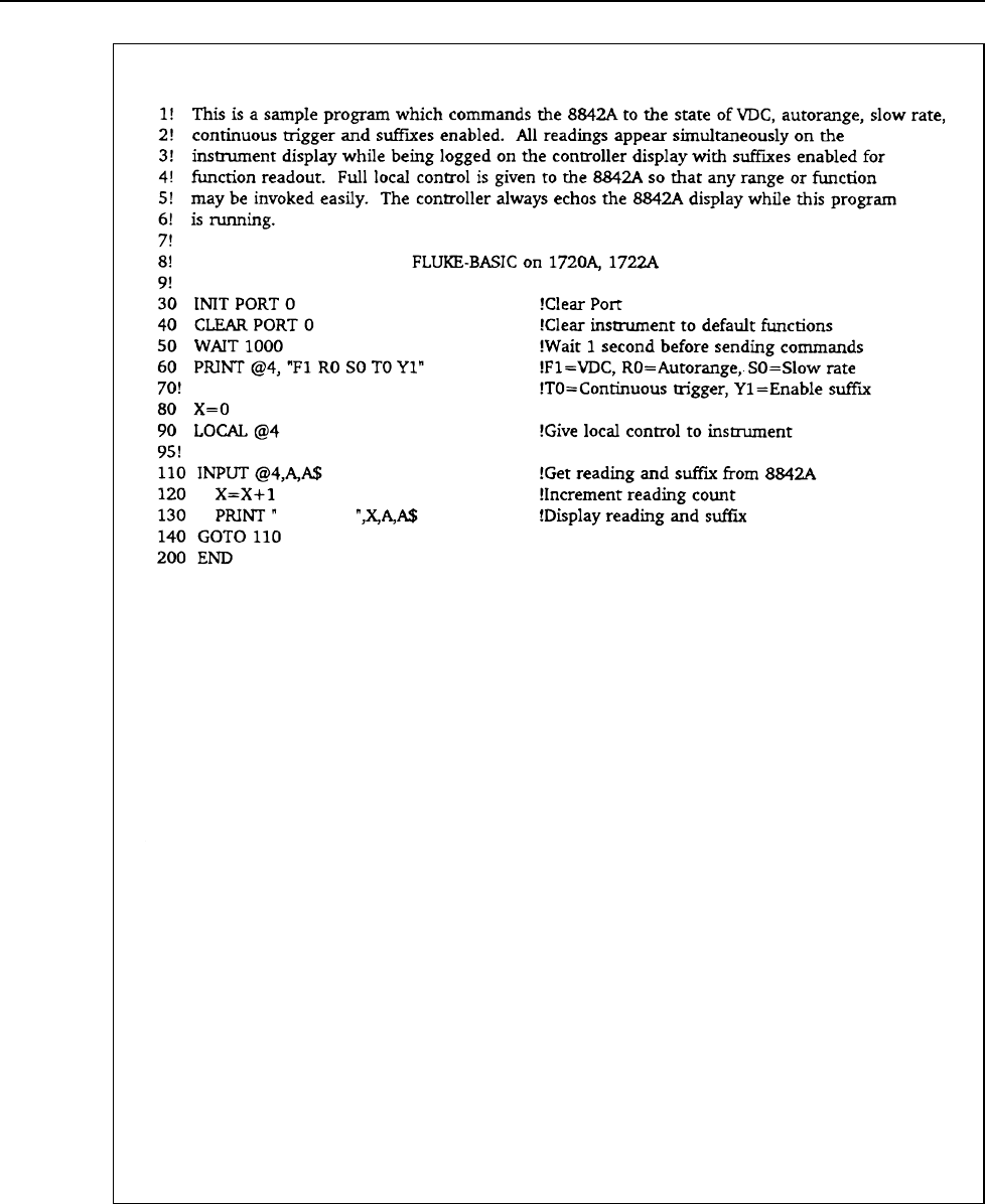
8842A
Instruction Manual
3-34
f3-11.wmf
Figure 3-10. Example Program: Taking Readings with Local Control
Remote Programming
EXAMPLE PROGRAMS
3
3-35
f3-12.wmf
Figure 3-11. Example Program: Using the Serial Poll Register
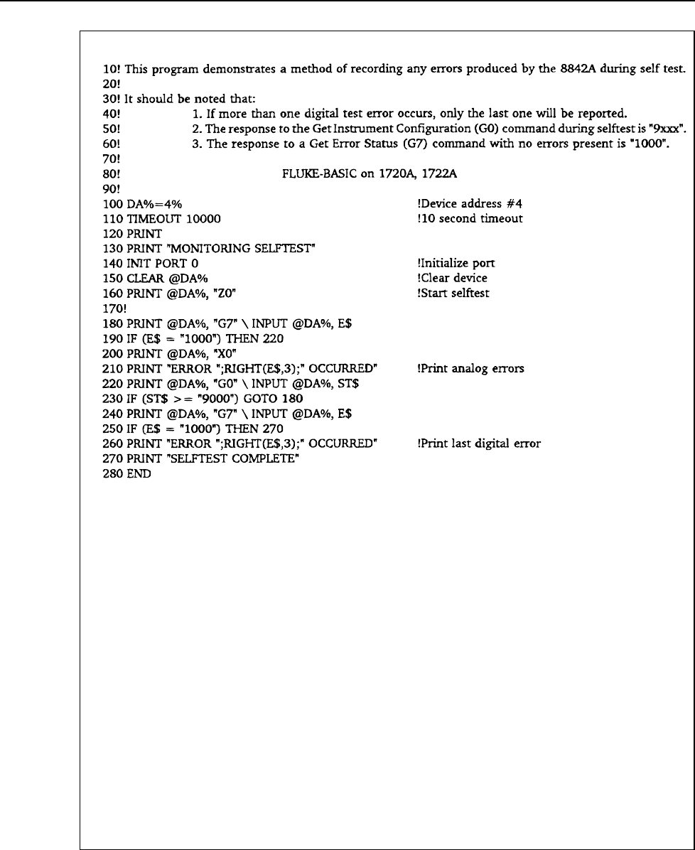
8842A
Instruction Manual
3-36
f3-13.wmf
Figure 3-12. Example Program: Record Errors During Selftest
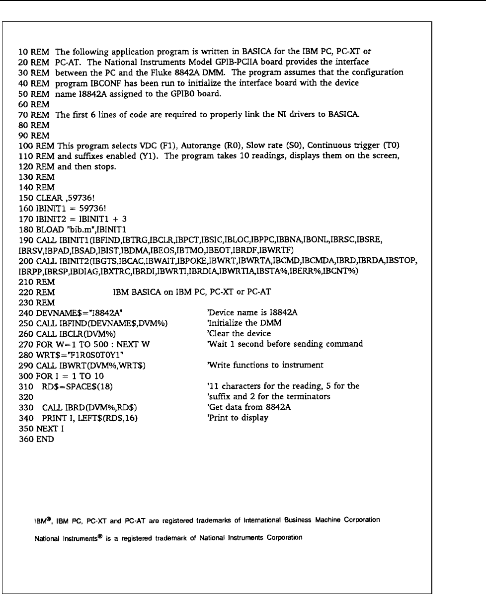
Remote Programming
EXAMPLE PROGRAMS
3
3-37
f3-14_01.wmf
Figure 3-13. Example Programs: Using the IBM PC
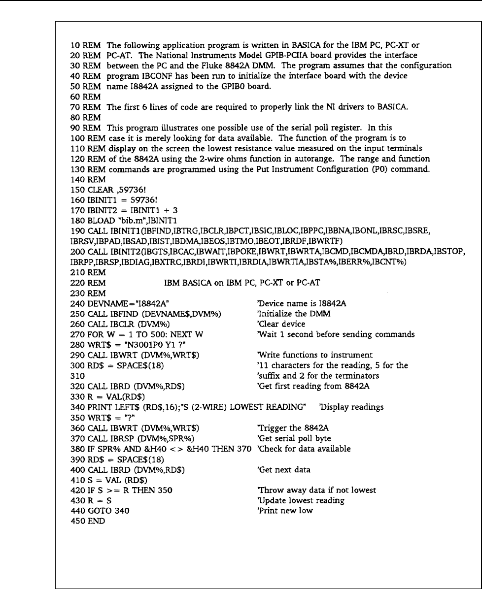
8842A
Instruction Manual
3-38
f3-14_01.wmf
Figure 3-14. Example Programs: Using the IBM PC (cont)
Remote Programming
EXAMPLE PROGRAMS
3
3-39
f3-14_02.wmf
Figure 3-14. Example Programs: Using the IBM PC (cont)
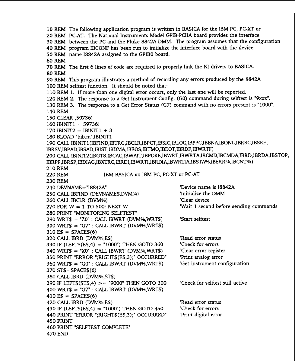
8842A
Instruction Manual
3-40
f3-14_03.wmf
Figure 3-14. Example Programs: Using the IBM PC (cont)
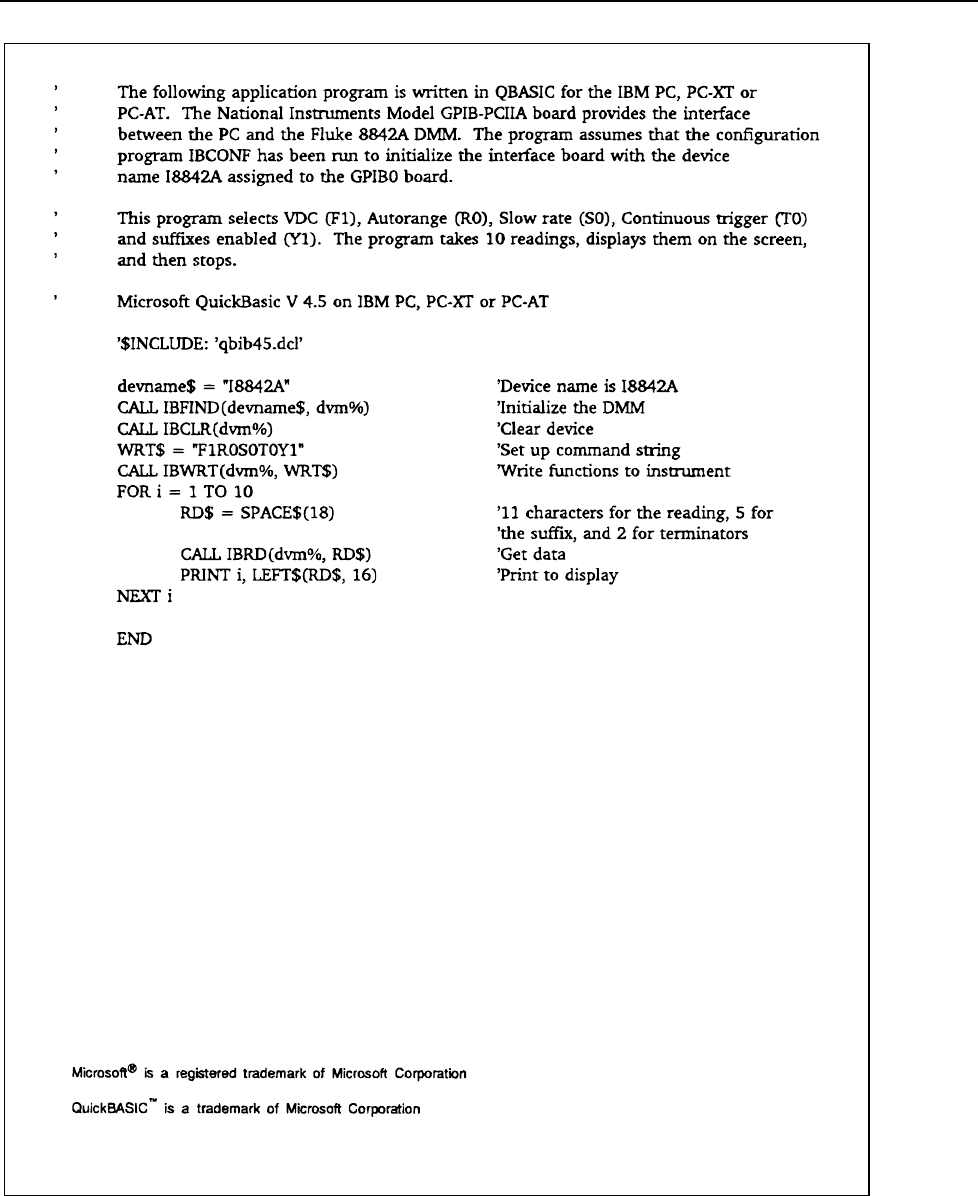
Remote Programming
EXAMPLE PROGRAMS
3
3-41
f3-14_04.wmf
Figure 3-14. Example Programs: Using the IBM PC (cont)
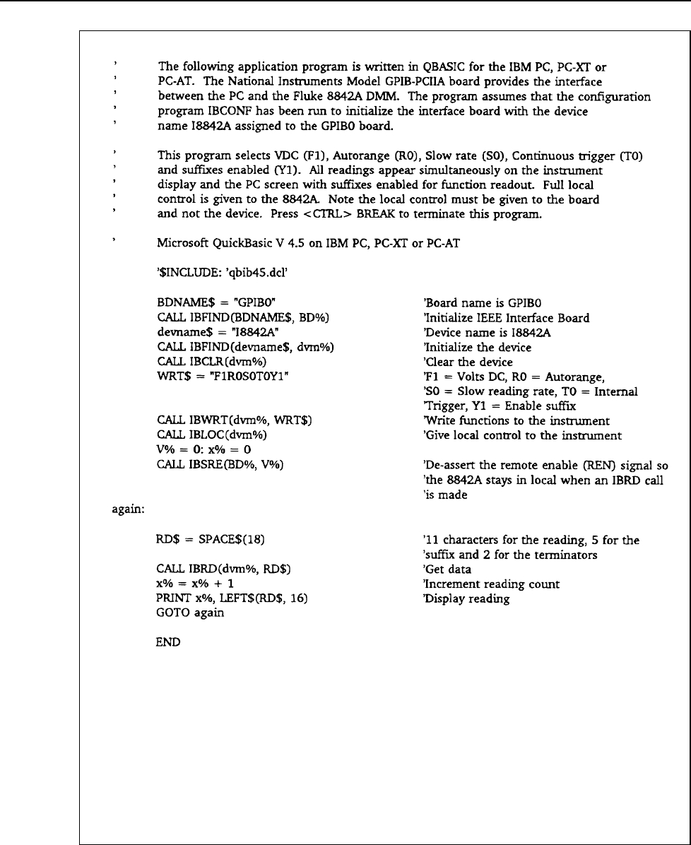
8842A
Instruction Manual
3-42
f3-14_05.wmf
Figure 3-14. Example Programs: Using the IBM PC (cont)
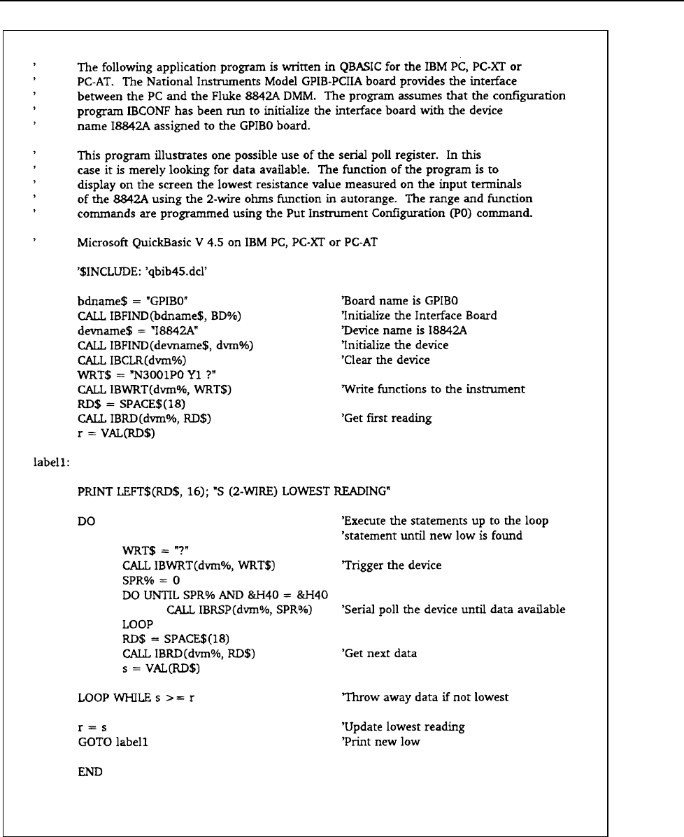
Remote Programming
EXAMPLE PROGRAMS
3
3-43
f3-14_06.wmf
Figure 3-14. Example Programs: Using the IBM PC (cont)
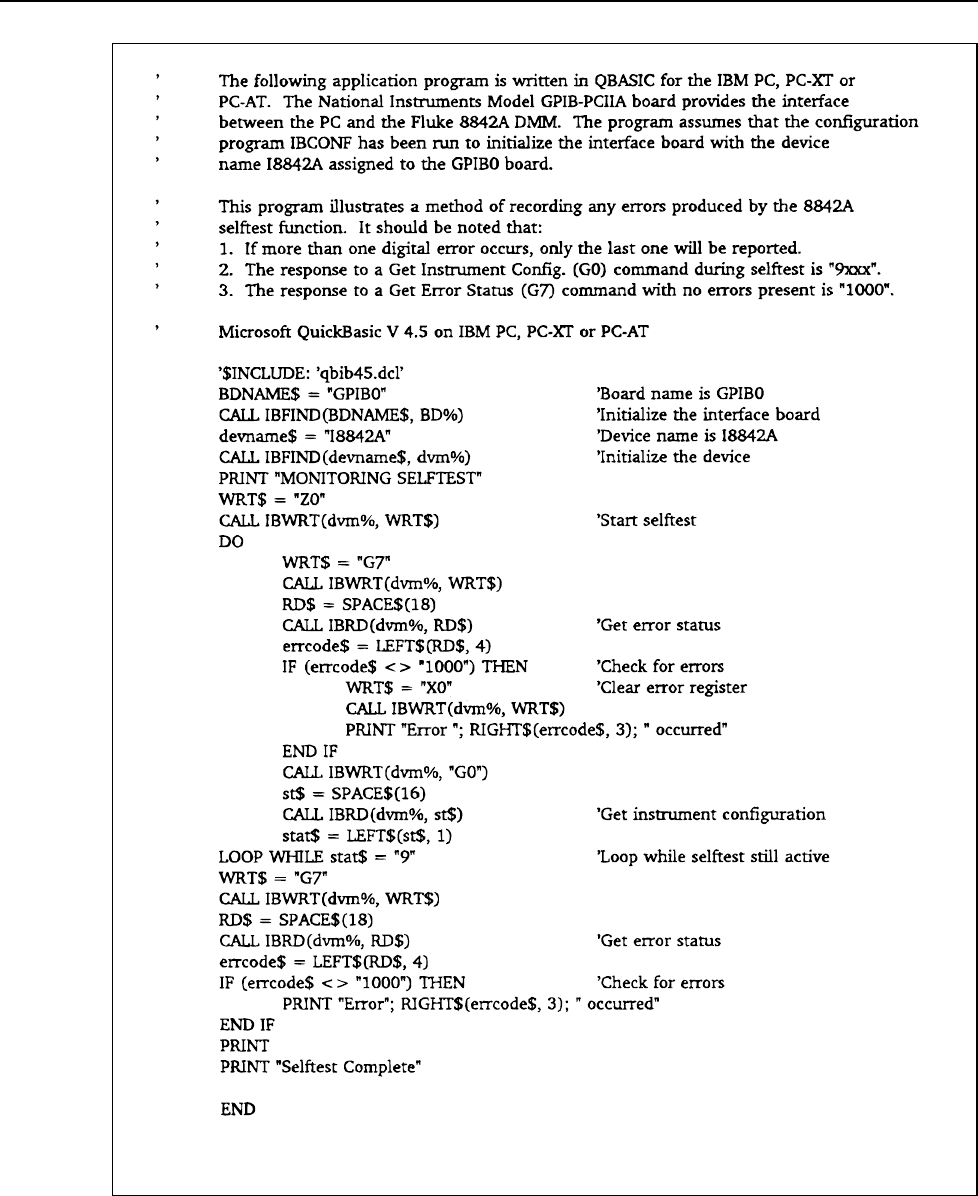
8842A
Instruction Manual
3-44
f3-14_07.wmf
Figure 3-14. Example Programs: Using the IBM PC (cont)
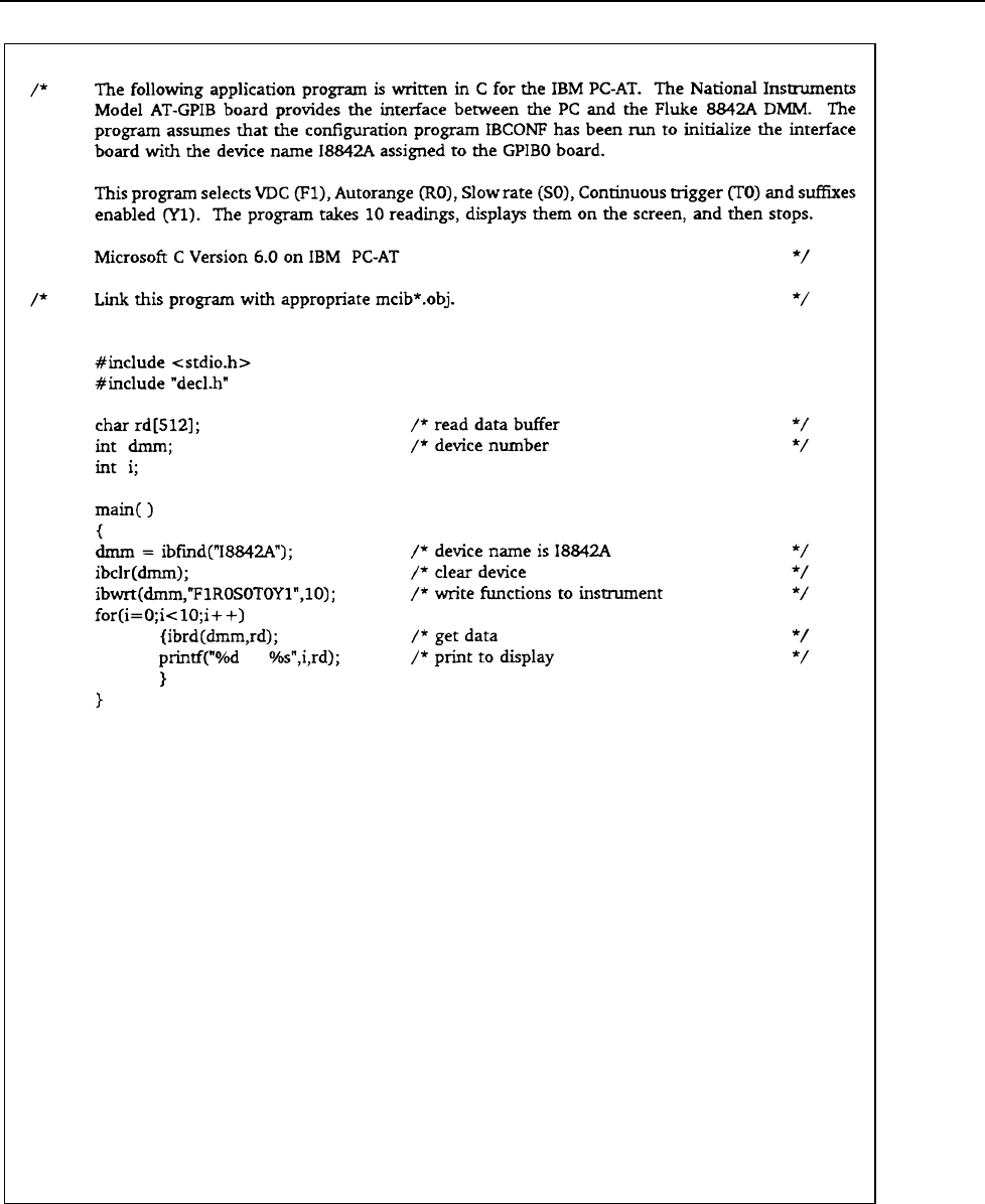
Remote Programming
EXAMPLE PROGRAMS
3
3-45
f3-14_08.wmf
Figure 3-14. Example Programs: Using the IBM PC (cont)
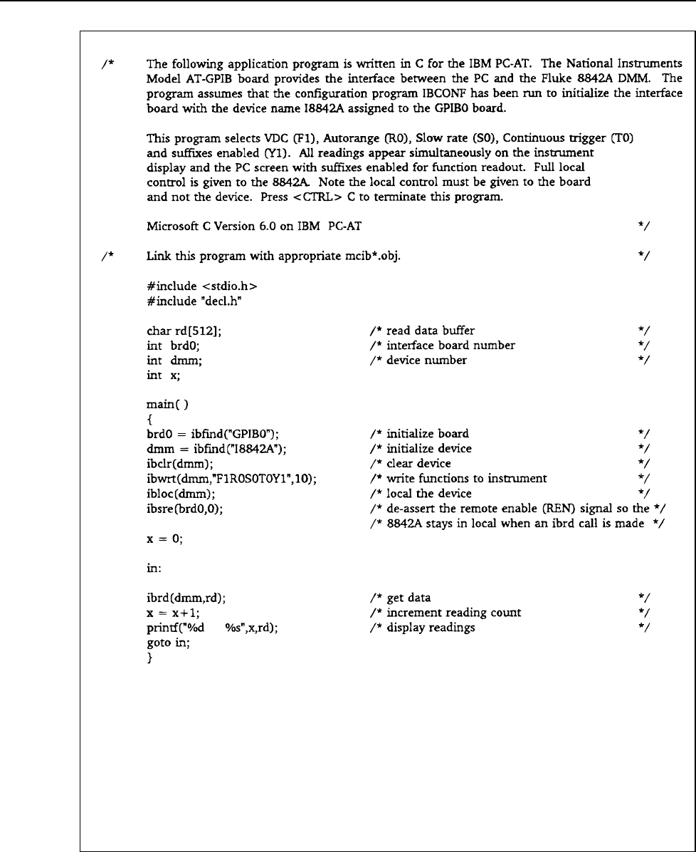
8842A
Instruction Manual
3-46
f3-14_09.wmf
Figure 3-14. Example Programs: Using the IBM PC (cont)
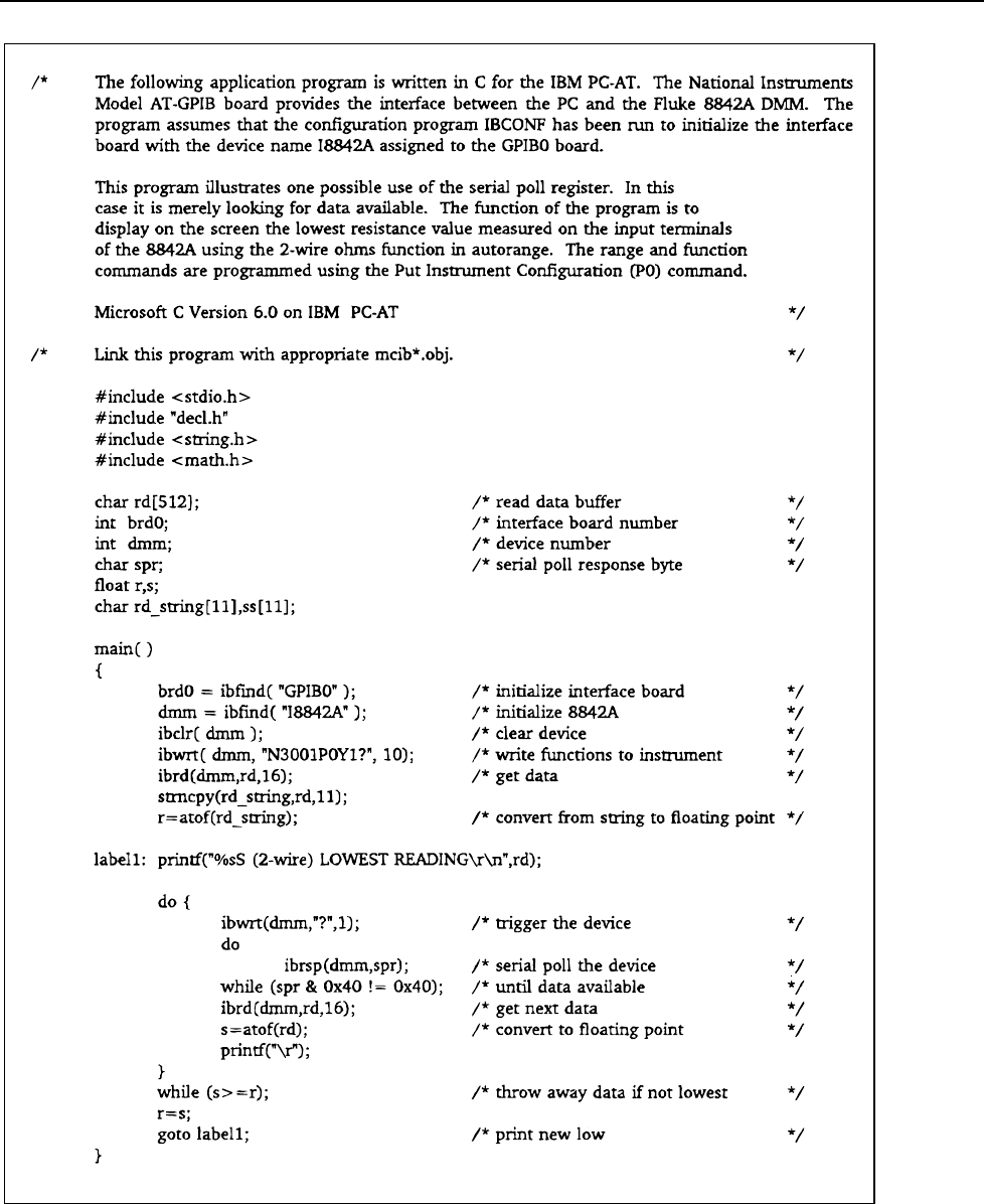
Remote Programming
EXAMPLE PROGRAMS
3
3-47
f3-14_10.wmf
Figure 3-14. Example Programs: Using the IBM PC (cont)
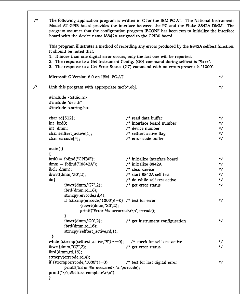
8842A
Instruction Manual
3-48
f3-14_11.wmf
Figure 3-14. Example Programs: Using the IBM PC (cont)
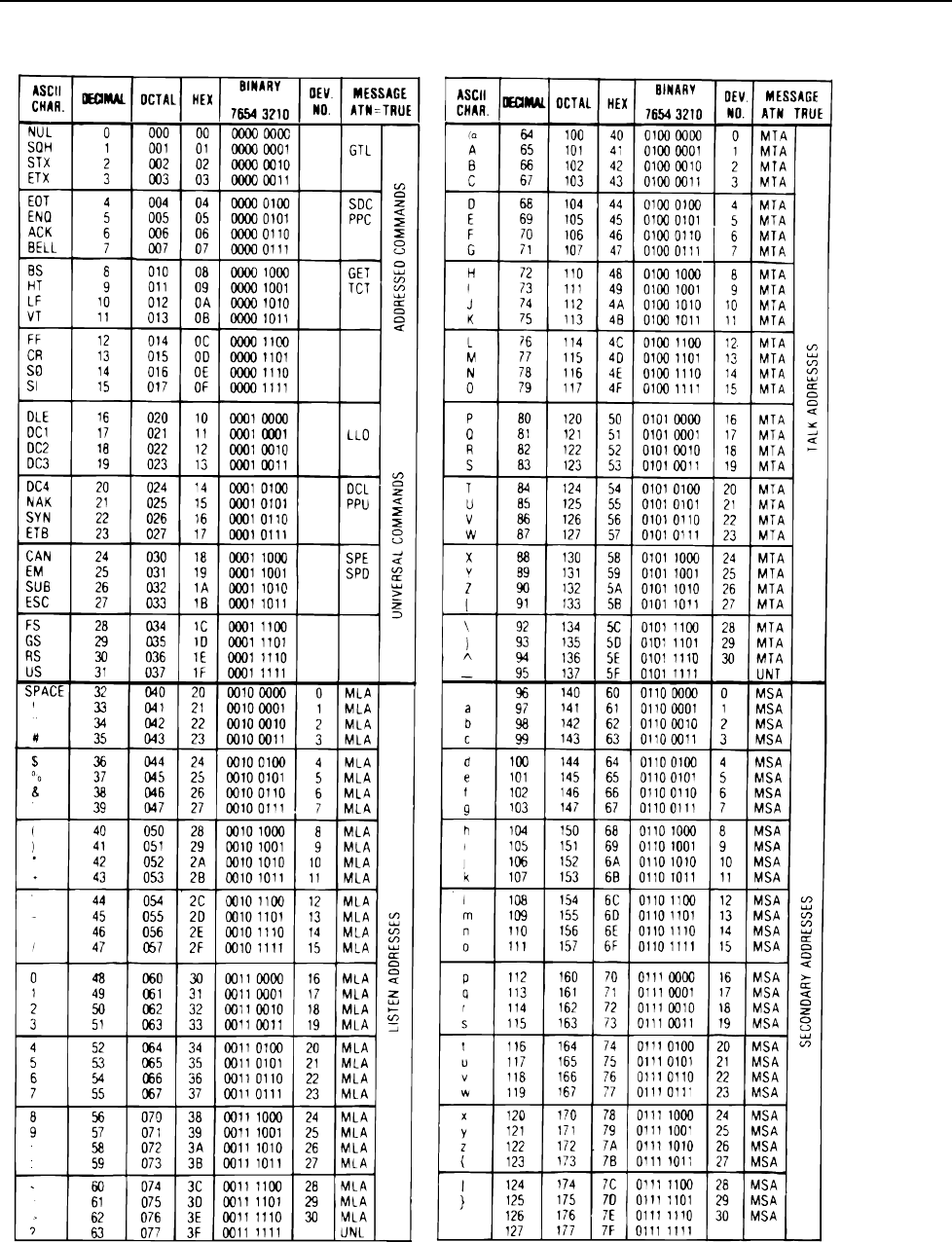
Remote Programming
EXAMPLE PROGRAMS
3
3-49
Table 3-4. ASCII/IEEE Std 488-1978 Bus Codes

8842A
Instruction Manual
3-50
NOTE
For the examples using the Fluke 1720A or 1722A, the 8842A is plugged
into port 0. The port is initialized by the INIT statement, which sends IFC
(interface clear).
4-1
Chapter 4
Measurement Tutorial
Title Page
4-1. INTRODUCTION................................................................................4-2
4-2. DC VOLTAGE MEASUREMENT .....................................................4-2
4-3. Circuit Loading Error.......................................................................4-2
4-4. Input Bias Current Error...................................................................4-3
4-5. RESISTANCE MEASUREMENT ......................................................4-4
4-6. 2-Wire Ohms....................................................................................4-4
4-7. Correcting for Test Lead Resistance in 2-Wire Ohms .....................4-5
4-8. 4-Wire Ohms....................................................................................4-5
4-9. Applications of the Ohms Functions................................................4-7
4-10. TESTING DIODES.....................................................................4-7
4-11. TESTING ELECTROLYTIC CAPACITORS ............................4-7
4-12. A PRECISION CURRENT SOURCE.........................................4-8
4-13. DC CURRENT MEASUREMENT .....................................................4-8
4-14. REDUCING THERMAL VOLTAGES...............................................4-9
4-15. AC VOLTAGE AND CURRENT MEASUREMENT........................4-10
4-16. True RMS Measurement..................................................................4-10
4-17. Waveform Comparison....................................................................4-10
4-18. Crest Factor......................................................................................4-12
4-19. AC-Coupled AC Measurements ......................................................4-12
4-20. Combined AC and DC Measurements.............................................4-13
4-21. Bandwidth ........................................................................................4-13
4-22. Zero-Input VAC Error......................................................................4-13
4-23. MAKING ACCURATE MEASUREMENTS ON THE 20 mV
AND 20Ω RANGES ............................................................................4-14
4-24. MAKING ACCURATE HIGH-RESISTANCE MEASUREMENTS .4-15
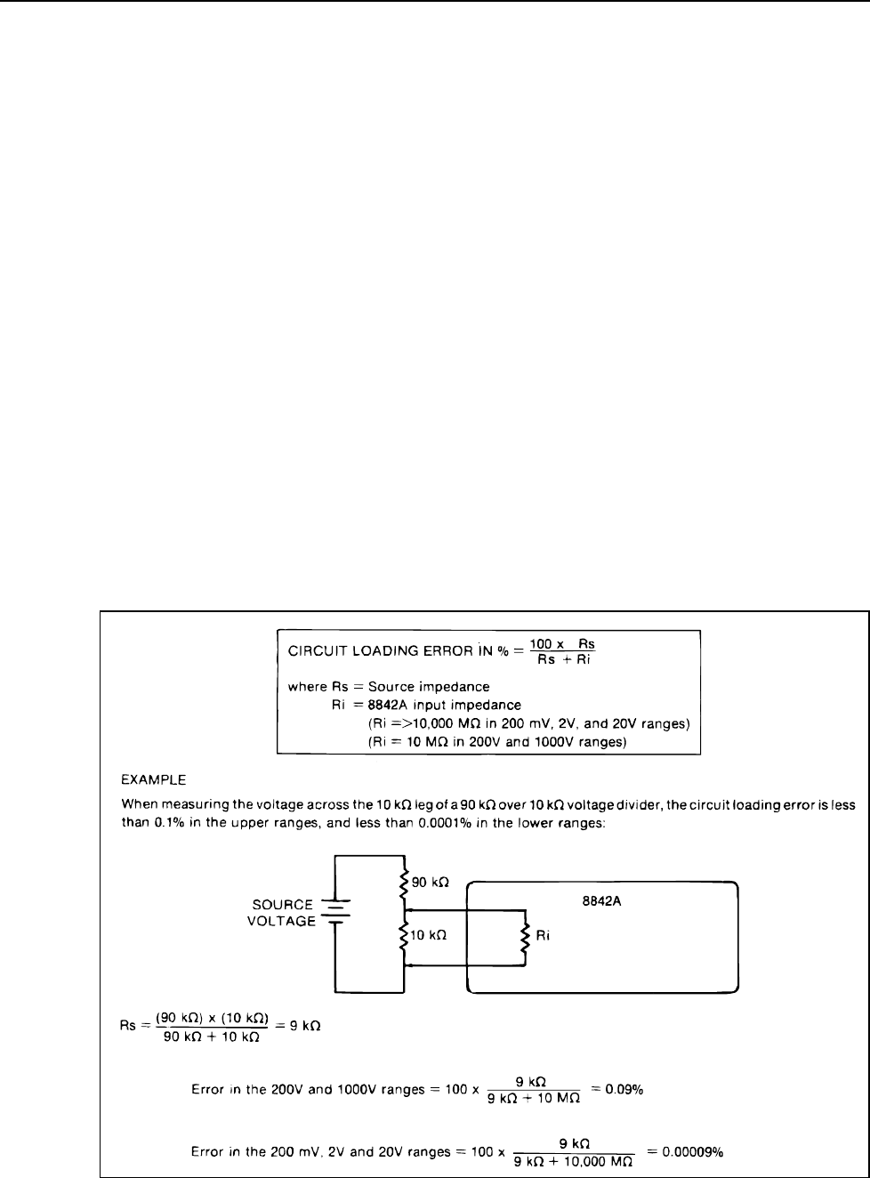
8842A
Instruction Manual
4-2
4-1. INTRODUCTION
This section discusses considerations and techniques to help you use the 8842A
effectively. Among other things, this section discusses sources of error which are an
inherent part of the measurement process and which occur for all multimeters. By
understanding why and when these errors occur, and by knowing how and when to
correct for them, you can make accurate measurements with confidence.
This section also discusses the relative benefits of 2-wire and 4-wire ohms, describes
special considerations for making ac measurements, and presents some unusual
applications--for example, using the test current in the 2-wire ohms function as a
troubleshooting tool in itself.
4-2. DC VOLTAGE MEASUREMENT
When measuring dc voltages in high-impedance circuits, there are two possible sources
of error to consider: circuit loading and input bias current.
4-3. Circuit Loading Error
Whenever a voltmeter is connected to a circuit, the voltmeter’s internal resistance changes
the voltage of the circuit under test. The resulting error is called circuit loading error. The
error is negligible as long as the resistance of the circuit under test (the source
impedance) is small compared to the input impedance of the meter. As the source
impedance approaches the input impedance of the voltmeter, the error can be
considerable. The percentage of error can be calculated using the formula in Figure 4-1.
f4-01.wmf
Figure 4-1. Circuit Loading Error Calculation
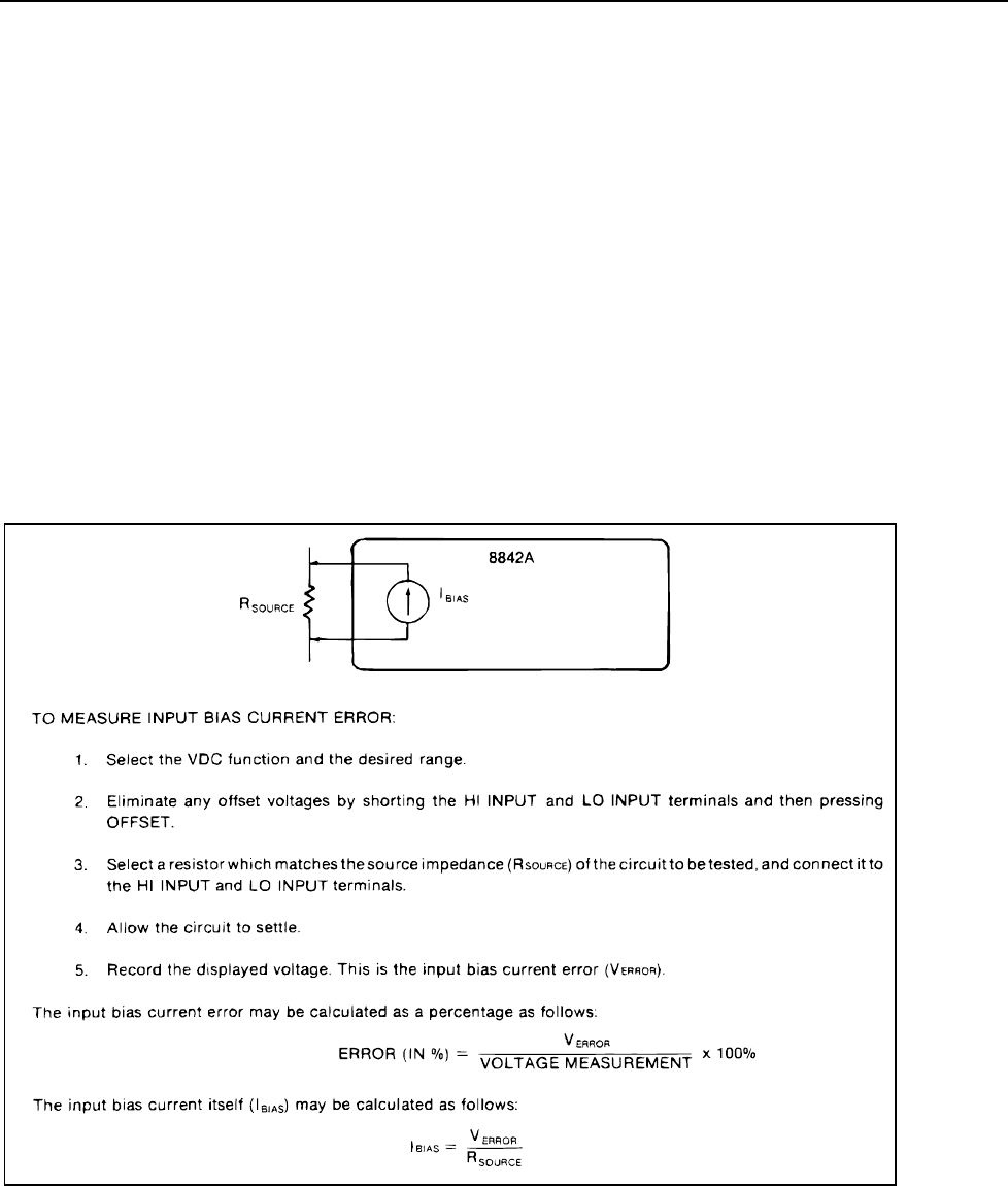
Measurement Tutorial
DC VOLTAGE MEASUREMENT
4
4-3
The input impedance of the 8842A is 10 MΩ in the 200V and 1000V dc ranges, and is
greater than 10,000 MΩ in the 20 mV, 200 mV, 2V, and 20V ranges. Therefore, for the
8842A, circuit loading error is less than 0.01% as long as the source impedance is less
than 1 MΩ in the 20 mV, 200 mV, 2V, and 20V ranges, and less than 1 kΩ in the 200V
and 1000V ranges. The exceptionally high input impedance on the 20V dc range allows
high-accuracy readings in CMOS and high-impedance analog circuitry.
NOTE
Input protection circuitry can reduce the input impedance to as low as 100
k
Ω
when the input is overrange. This may also occur momentarily when the
instrument autoranges to a higher range.
4-4. Input Bias Current Error
Input bias current error occurs because a voltmeter’s input bias current always changes
the voltage of the circuit under test. However, the error is significant only when
measuring voltages in circuits with very high source impedance. The error can be
measured as shown in Figure 4-2.
f4-02.wmf
Figure 4-2. Measuring Input Bias Current Error
With the 8842A, it is easy to correct for this error using the OFFSET button:
1. Select the VDC function and the desired range.
2. Connect the 8842A INPUT terminals to a resistor which matches the source
impedance of the circuit to be tested.
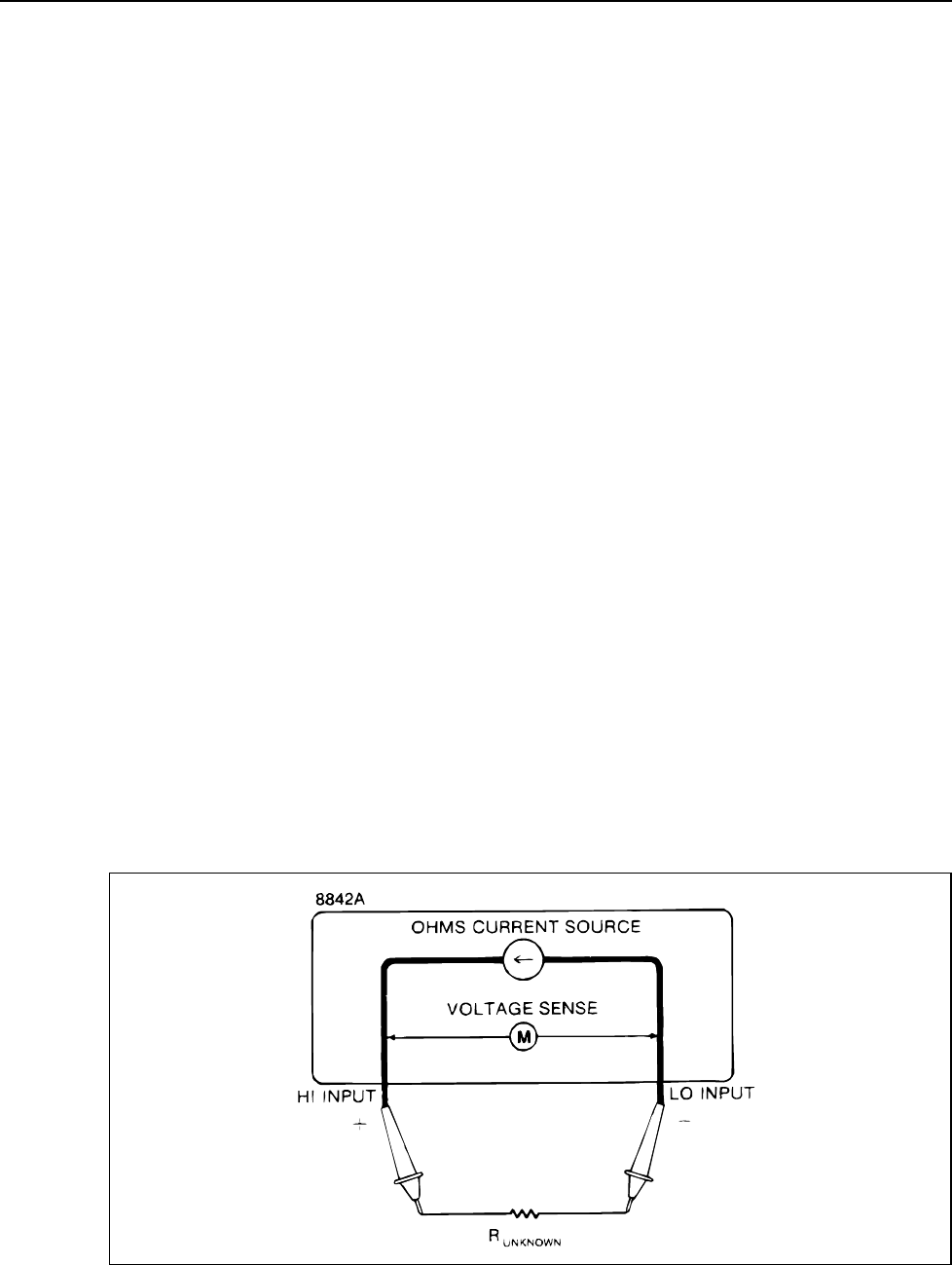
8842A
Instruction Manual
4-4
3. Allow the displayed reading to settle.
4. Press the OFFSET button.
5. Remove the resistor.
6. Proceed with the desired measurement.
Example:
Measure a 1.5V source with 1 MΩ source impedance, correcting for input bias current.
1. Connect a 1 MΩ resistor between the INPUT HI and INPUT LO terminals.
2. Select the VDC function and the 2V range.
3. Allow the display to settle.
4. Press OFFSET. (This zeroes the input bias current error.)
5. Remove the 1 MΩ resistor.
6. Measure the voltage of the circuit under test.
Note that this procedure does not correct for circuit loading error. Also note that if input
bias current error is not corrected for, it may be added to the circuit loading error.
4-5. RESISTANCE MEASUREMENT
The 8842A allows you to measure resistance in both 2-wire and 4-wire configurations.
Each has its benefits.
4-6. 2-Wire Ohms
Two-Wire ohms measurements are simple to set up and yield good results for most
measurement conditions. Measurements are made as shown in Figure 4-3. An internal
current source (the "ohms current source") passes a known test current (Itest) through the
resistance being tested (Runknown). The 8842A measures the voltage drop across
Runknown, calculates Runknown using Ohm’s law (Runknown = Vtest/Itest), and
displays the result.
f4-03.wmf
Figure 4-3. Wire Ohms Measurement

Measurement Tutorial
RESISTANCE MEASUREMENT
4
4-5
The test current and full-scale voltage for each resistance range are shown in Table 4-1.
Since the HI INPUT test lead is positive with respect to the LO INPUT lead, these test
leads are not interchangeable when a semiconductor device is being measured.
4-7. Correcting for Test Lead Resistance in 2-Wire Ohms
In 2-wire ohms, the resistance of the test leads can introduce error when measuring low
resistances. Typical test leads may add as much as 0.5Q to 2-wire ohms readings.
With the 8842A, it is easy to correct for this error using the OFFSET button:
1. Select the 2-wire ohms function.
2. Touch the test leads together. The 8842A should indicate the resistance of the test
leads.
3. With the test leads still touching, press the OFFSET button.The 8842A should read
0Ω.
4-8. 4-Wire Ohms
Four-Wire ohms measurements provide the highest accuracy for low resistance
measurements. The 4-wire configuration automatically corrects for both test lead
resistance and contact resistance. Contact resistance (the resistance between the test probe
tips and the circuit being tested) is unpredictable, and therefore cannot be reliably
corrected with a fixed offset.
Four-Wire ohms measurements are especially important when using long test leads. In a
typical automated test system, for example, the test leads could be connected through
four or five switching relays, each with 2Ω of resistance!
NOTE
Instability of the test lead’s resistance can cause significant error on low
ohms ranges, particularly on the 20
Ω
and 200
Ω
ranges. Therefore, only 4-
wire ohms measurement is permitted in the 20
Ω
range.
The 8842A makes 4-wire ohms measurements as shown in Figure 4-4. The HI and LO
INPUT leads apply a known, internal current source to the unknown resistance, just as in
2-wire ohms. (See Table 4-1.) However, the voltage drop across the unknown resistance
is measured with the SENSE leads rather than the INPUT leads. Since the current flow in
the SENSE leads is negligible, the error caused by the voltage drop across the leads is
also negligible.
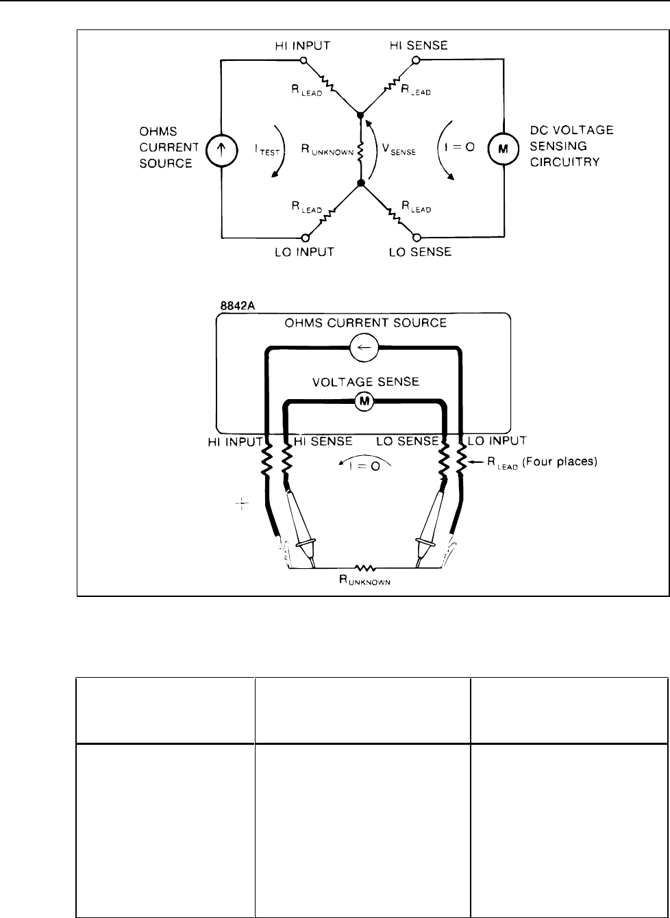
8842A
Instruction Manual
4-6
f4-04.wmf
Figure 4-4. Wire Ohms Measurement
Table 4-1. Ohms Test Current
RANGE TEST CURRENT FULL SCALE VOLTAGE
20Ω1 mA 0.02V
200Ω1 mA 0.2V
2 kΩ1 mA 2.0V
20 kΩ100 µA2.0V
200 kΩ10 µA2.0V
2000 kΩ5 µA 10.0V
20 MΩ500 nA 10.0V

Measurement Tutorial
RESISTANCE MEASUREMENT
4
4-7
NOTE
In the 2 M
Ω
and 20 M
Ω
ranges of 4-wire ohms, the voltage across the
unknown resistance is sensed between the HI SENSE and LO INPUT
terminals. Accuracy is not affected as long as the resistance of the LO
INPUT lead is less than 10
Ω
in the 2 M
Ω
range, and less than 100
Ω
in the
20 M
Ω
range.
4-9. Applications of the Ohms Functions
The 2-wire and 4-wire ohms functions can be used for a variety of purposes in addition to
measuring resistance, as the following applications show.
4-10. TESTING DIODES
The 2-wire ohms function can also be used to test diodes.
1. Select the 2-wire ohms function and the 2 kΩ range.
2. Measure the resistance of the diode. If the diode is good, when forward-biased it will
measure about 0.6 kΩ to 0.7 kΩ for silicon (0.25 kΩ to 0.3 kΩ for germanium), and
when reverse-biased it will cause the 8842A to indicate overrange. (The forward-
biased reading depends upon the range used.)
The 2 kΩ range is used because its 1 mA test current provides a typical operating point,
and its 2V full-scale voltage is sufficient to turn on most diodes (even two diodes in
series).
4-11. TESTING ELECTROLYTIC CAPACITORS
The 2-wire ohms function can also give a rough test of an electrolytic capacitor’s leakage
and dielectric absorption. This test works well for capacitors 0.5 µF and larger.
1. Select the 2-wire ohms function, the 2 kΩ range, and the medium reading rate.
2. Connect the test leads to the capacitor (with the INPUT HI lead to the + lead and the
INPUT LO lead to the - lead). The 8842A attempts to charge it to the open-circuit
voltage of the 2 kΩ range (about 6V).
3. Disconnect the + test lead.
4. To test for leakage, select the VDC function and the 20V range (leave the 8842A in
the medium reading rate), and measure the voltage that was stored on the capacitor
during step 2.
a. If the capacitor is good, the voltage across the capacitor will be about 6V, and
will be relatively stable.
b. If the capacitor is leaky, the voltage across the capacitor will be much less than
6V, and the voltage will be decreasing. The rate of change depends on how leaky
the capacitor is.
c. With some electrolytic capacitors, the reading will increase. This usually
indicates the capacitor is defective.
5. To test the capacitor’s dielectric absorption, briefly short the capacitor’s leads together
and then measure the voltage across the capacitor.
a. If the dielectric is good (i.e., has low dielectric absorption), the voltage across the
capacitor will be nearly zero volts.
b. If the dielectric is poor (i.e., has high dielectric absorption), the voltage across the
capacitor will be significantly above zero.

8842A
Instruction Manual
4-8
4-12. A PRECISION CURRENT SOURCE
The ohms current source (the internal current source used in the ohms functions) makes a
useful troubleshooting tool in itself. It has excellent linearity and temperature stability. Its
compliance voltage is typically 5V in the lower five ohms ranges, and 12V in the upper
two ohms ranges. The inputs are protected against accidental applications of voltage up to
300V rms.
To use the ohms current source, connect the test leads to the HI and LO INPUTS, and
select either the 2-wire or 4-wire ohms function. Press the range buttons to select any of
the current levels shown in Table 4-1.
The ohms current source can be used to troubleshoot circuits by injecting current into
selected nodes, forcing the circuits to be in a specific test state. For example, the ohms
current source can be used to set or modify the bias of amplifier circuits. The current
level can be changed simply by changing range.
The ohms current source can also be used to test mA or µA panel meters. The accuracy
of the current source is more than enough to verify panel meters, whose accuracy is
typically 1% to 5%. To test an analog panel meter, simply connect the current source
across the meter movement (as though measuring its resistance). A 1 mA meter should
show full scale when the ohms function is set on the 2 kΩ range. The same technique also
works with digital panel meters.
4-13. DC CURRENT MEASUREMENT
To get the best accuracy using the mA DC function, it is important to understand the
concept of burden voltage error.
When a meter is placed in series with a circuit to measure current, error can be caused by
the small voltage drop across the meter (in this case, across the protective fuses and
current shunt). This voltage drop is called the burden voltage, and it is highest for full-
scale measurements. The full-scale burden voltage for the 8842A is typically less than
1V.
The burden voltage can present a significant error if the current source being measured is
unregulated (i.e., not a true current source) and if the resistance of the fuse and shunt is a
significant part of the source resistance. If burden voltage does present a significant error,
the percentage of error can be calculated and corrected for using the formulas in Figure 4-
5.
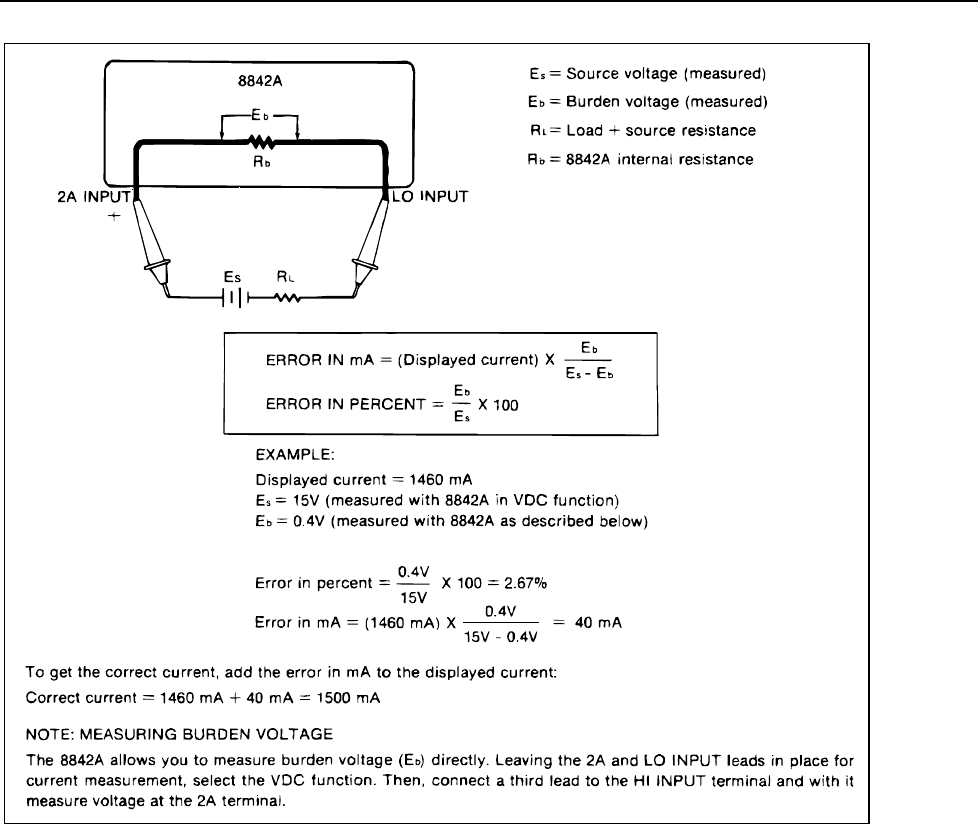
Measurement Tutorial
REDUCING THERMAL VOLTAGES
4
4-9
f4-05.wmf
Figure 4-5. Burden Voltage Error Calculation
4-14. REDUCING THERMAL VOLTAGES
When making very low-level dc measurements, thermal voltages can present an
additional source of error. Thermal voltages are the thermovoltaic potentials generated at
the junction between dissimilar metals. Thermal voltages typically occur at binding posts
and can be greater than 10 µV.
Thermal voltages can also cause problems in the low dc and ohms ranges, particularly in
the 20 mV and 20Ω ranges. Some low-value resistors are constructed with dissimilar
metals. Just handling such resistors can cause thermal voltages large enough to introduce
measurement errors.
The effect of thermal voltages can be reduced by using the following techniques:
1. Use tight connections.
2. Use clean connections (especially free of grease and dirt).
3. Use similar metals for connections wherever possible (e.g., copper-to-copper, gold-
to-gold, etc.).

8842A
Instruction Manual
4-10
4. Use caution when handling the circuit under test.
5. Wait for the circuit to reach thermal equilibrium. (Thermal voltages are generated
only where there is a temperature gradient.)
4-15. AC VOLTAGE AND CURRENT MEASUREMENT
When making precise measurements of ac voltage and current, there are several
considerations in addition to those discussed under dc voltage and current measurement.
These include the concepts of rms conversion, crest factor, bandwidth, and zero-input
error.
4-16. True RMS Measurement
The True RMS AC Option measures the true rms value of ac voltages and currents. In
physical terms, the rms (root-mean-square) value of a waveform is the equivalent dc
value that causes the same amount of heat to be dissipated in a resistor. True rms
measurement greatly simplifies the analysis of complex ac signals. Since the rms value is
the dc equivalent of the original waveform, it provides a reliable basis for comparing
dissimilar waveforms.
By contrast, many meters in use today use average-responding ac converters rather than
true rms converters. The scale factor in these meters is adjusted so that they display the
rms value for harmonic-free sinusoids. However, if a signal is not sinusoidal, average-
responding meters do not display correct rms readings.
The 8842A actually derives the rms value using analog computation. This means that the
8842A readings represent true rms values not only for harmonic-free sinusoids, but also
for mixed frequencies, modulated signals, square waves, sawtooths, random noise,
rectangular pulses with 10% duty cycle, etc.
4-17. Waveform Comparison
Figure 4-6 illustrates the relationship between ac and dc components for common
waveforms, and compares readings for true rms meters and average-responding meters.
For example, consider the first waveform, a 1.41421V (zero-to-peak) sine wave. Both the
8842A and rms-calibrated average-responding meters display the correct rms reading of
1.00000V (the dc component equals 0). However, consider the 2V (peak-to-peak) square
wave. Both types of meter correctly measure the dc component (0V), but only the 8842A
correctly measures the ac component (1.00000V). The average-responding meter
measures 1.110V, which amounts to an 11% error.
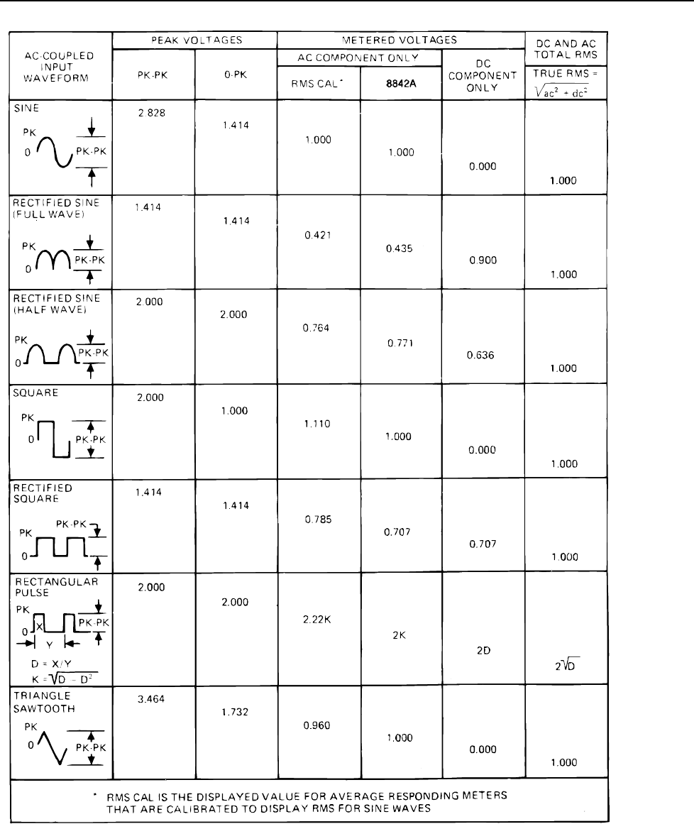
Measurement Tutorial
AC VOLTAGE AND CURRENT MEASUREMENT
4
4-11
f4-06.wmf
Figure 4-6. Waveform Comparison Chart
Since average-responding meters have been in use for so long, you may have
accumulated test or reference data based on them. The conversion factors in Figure 4-6
should help you convert between the two measurement methods.
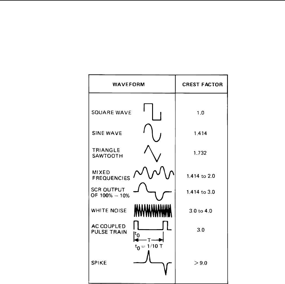
8842A
Instruction Manual
4-12
4-18. Crest Factor
Crest factors are useful for expressing the ability of an instrument to measure a variety of
waveforms accurately. The crest factor of a waveform is the ratio of its peak voltage to its
rms voltage. (For waveforms where the positive and negative half-cycles have different
peak voltages, the more extreme peak is used in computing the crest factor.) Crest factors
start at 1.0 for square waves (for which the peak voltage equals the rms voltage) and
increase for more "pointed" waveforms as shown in Figure 4-7.
f4-07.wmf
Figure 4-7. Typical Crest Factors for Various Waveforms
The 8842A has a full-scale crest factor limit of 3.0 for the 20V and 700V ranges, and 6.0
for the other ranges. For full-scale input signals with a crest factor above these limits,
dynamic range limitations can begin to cause large errors. However, as Figure 4-7 shows,
signals with a crest factor above 3.0 are unusual.
If you don’t know the crest factor of a particular waveform but wish to know if it falls
within the crest factor limit of the 8842A, measure the signal with both the 8842A and an
ac-coupled oscilloscope. If the rms reading on the 8842A is 1/3 or more of the
waveform’s zero-to-peak voltage, the crest factor is 3.0 or less.
4-19. AC-Coupled AC Measurements
Input signals are ac-coupled in the ac functions. One of the advantages of ac coupling is
that ac measurements can be made on power supply outputs, phone lines, etc. Ripple
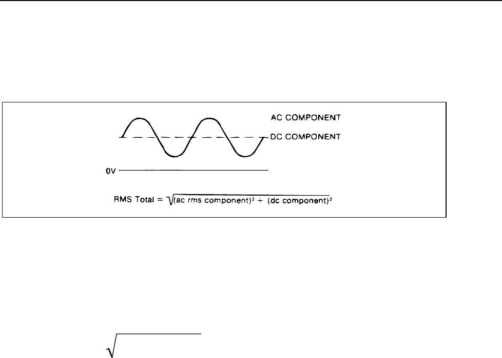
Measurement Tutorial
AC VOLTAGE AND CURRENT MEASUREMENT
4
4-13
measurements, for instance, cannot be made with dc coupling. Remember, however, that
when the 8842A measures signals with the ac functions, the reading on the display does
not include the dc component (if one exists). For example, consider Figure 4-8, which
shows a simple ac signal riding on a dc level. The VAC function would measure the ac
component only.
f4-08.wmf
Figure 4-8. Combined AC and DC Measurement
4-20. Combined AC and DC Measurements
The 8842A can be used to evaluate the true rms value of waveforms such as the one
shown in Figure 4-8, which includes both ac and dc components. First, measure the rms
value of the ac component using the VAC function. Next, measure the dc component
using the VDC function. Finally, calculate the total rms value as follows:
22
RMSVDCAC VV +=
4-21. Bandwidth
Bandwidth defines the range of frequencies to which an instrument can respond
accurately. The accuracy of the 8842A is specified for sinusoidal waveforms up to 100
kHz, or for nonsinusoidal waveforms with frequency components up to 100 kHz. The
small-signal bandwidth (the frequency at which the response is 3 dB down) is typically
around 300 kHz.
For signals with components greater than 100 kHz, the measurement accuracy is reduced
because of frequency bandwidth and slew-rate limitations. Because of this, accuracy may
be reduced when measuring signals with fast rise times, such as high-frequency square
waves or switching supply waveforms. As a rule of thumb, an ac voltage input signal is
within the bandwidth limitations if the rise time is longer than 2 us, and within the slew-
rate limitations if the input slew rate is slower than (1V/µs)x(full scale of range).
4-22. Zero-Input VAC Error
If the 8842A input terminals are shorted while the VAC function is selected, the 8842A
displays a non-zero reading (typically less than 80 digits in the highest four ranges, and
less than 300 digits in the 200 mV range). Such readings are due to random noise
combined with the inherent nonlinear response of computing-type rms converters to very
small input signals.
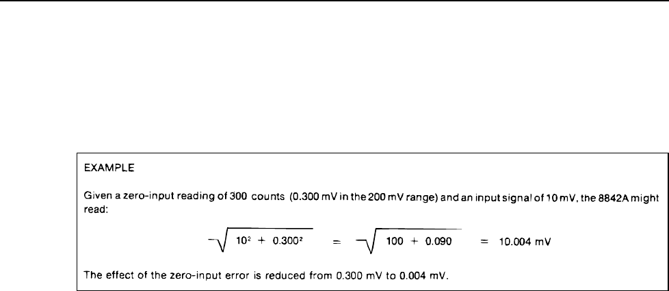
8842A
Instruction Manual
4-14
The zero-input error is quickly reduced when the input is increased. The rms converter
error (a dc error) and the internally generated noise (a random ac error) are both
uncorrelated with the input signal. Therefore, when a signal is applied, the resulting
reading is not the simple addition of the signal and the zero-input error, but the square
root of the sum of their squares. This reduces the effect of the error, as shown in the
example in Figure 4-9.
f4-09.wmf
Figure 4-9. Reduction of Zero-Input Error
As long as the 8842A reading is 1,000 counts or more, readings will still be within
specified accuracy.
4-23. MAKING ACCURATE MEASUREMENTS ON THE 20 mV
AND 20
Ω
RANGES
NOTE
When making low-level (uV) measurements after a large step signal has
been applied to the inputs, allow sufficient time for thermal emfs and other
system-related sources of error to settle before taking readings.
The 20 mV dc and 20Ω ranges are the 8842A’s most sensitive ranges. For that reason,
they are also the most susceptible to error from electrical noise, thermal voltages, and (for
resistance measurements) test lead resistance. You can minimize these sources of error by
using good measurement practices.
The most common source of error is electrical noise. Typical sources of noise include
electrostatic noise, inductive pickup noise, radio frequency noise, power line noise and
noise generated by ground loop currents. Noise pickup can be minimized by properly
shielding the test leads between the 8842A and the signal source.
For voltage measurements in most system applications, where common-mode voltages
are typically present, connect the test lead shielding to the 8842A INPUT LO terminal as
shown in Figure 4-10. This configuration minimizes the error caused by current that
would flow in the leads due to common-mode voltages between the measurement and
stimulus points and instrument ground. The 8842A’s INPUT LO terminal is internally
connected to the instrument’s internal guard, which provides a shield between the
instrument’s ground and its sensitive analog circuits. The 8842A’s analog circuits are
isolated from its digital circuits by an electrostatically shielded transformer, whose shield
is also connected to the guard.
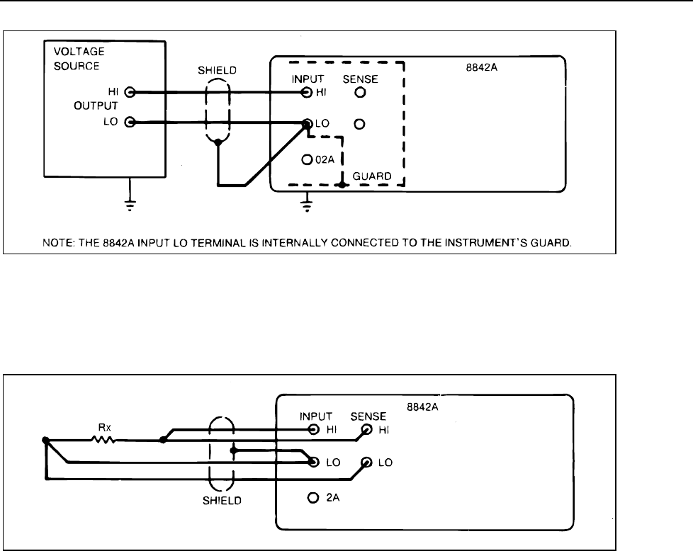
Measurement Tutorial
MAKING ACCURATE HIGH-RESISTANCE MEASUREMENTS
4
4-15
f4-10.wmf
Figure 4-10. Shielding for Low Voltage Measurements
For low-level resistance measurements, connect the test lead shielding as shown in Figure
4-11. Use the 4-wire ohms function to minimize the error caused by the resistance of the
test leads.
f4-11.wmf
Figure 4-11. Shielding for Low Resistance Measurements
Errors due to thermal voltages should also be considered when making low-level voltage
or resistance measurements. Techniques for reducing thermal voltages are presented
earlier in this section.
4-24. MAKING ACCURATE HIGH-RESISTANCE
MEASUREMENTS
When high resistances are measured (typically 1 MΩ or greater), leakage resistance at the
test circuit can provide enough shunt resistance to degrade the accuracy of the
measurement (see Figure 4-12). To minimize leakage resistance, watch out for
contamination, high humidity, poor-quality interconnections, and poor-quality insulation
of the stand-offs on which test resistors are mounted.
High-resistance measurements are also susceptible to error from electrical noise pickup.
For accurate measurements, use short test leads and enclose the test leads and test circuit
in a proper shield that is connected to the 8842A’s INPUT LO terminal. Pickup of slowly
fluctuating noise can also be reduced by using the OFFSET feature as described in
paragraph 4-7.
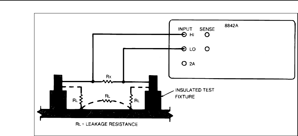
8842A
Instruction Manual
4-16
f4-12.wmf
Figure 4-12. Leakage Resistance in High Resistance Measurement
5-1
Chapter 5
Theory of Operation
Title Page
5-1. INTRODUCTION................................................................................ 5-3
5-2. OVERALL FUNCTIONAL DESCRIPTION...................................... 5-3
5-3. DETAILED CIRCUIT DESCRIPTION .............................................. 5-4
5-4. DC SCALING ...................................................................................... 5-4
5-5. VDC Scaling .................................................................................... 5-6
5-6. VDC Protection................................................................................ 5-7
5-7. mA DC Scaling................................................................................ 5-7
5-8. Analog Filter .................................................................................... 5-7
5-9. TRACK/HOLD CIRCUIT ................................................................... 5-8
5-10. Track Configuration......................................................................... 5-10
5-11. Settling Configuration...................................................................... 5-11
5-12. Hold Configuration .......................................................................... 5-11
5-13. Pre-Charge Configuration................................................................ 5-11
5-14. PRECISION VOLTAGE REFERENCE.............................................. 5-11
5-15. OHMS CURRENT SOURCE .............................................................. 5-12
5-16. OHMS PROTECTION......................................................................... 5-13
5-17. OHMS FUNCTIONS ........................................................................... 5-13
5-18. 2-Wire Ohms.................................................................................... 5-13
5-19. 4-Wire Ohms.................................................................................... 5-15
5-20. A/D CONVERTER .............................................................................. 5-15
5-21. Timing/Data Control........................................................................ 5-17
5-22. Precision DAC ................................................................................. 5-17
5-23. A/D Amplifier.................................................................................. 5-18
5-24. Bootstrap Supplies ........................................................................... 5-18
5-25. DISPLAY ............................................................................................. 5-18
5-26. KEYBOARD........................................................................................ 5-19
5-27. DIGITAL CONTROLLER................................................................... 5-19
5-28. In-Guard Microcomputer ................................................................. 5-21
5-29. Function and Range Control ............................................................ 5-23
5-30. A/D Control and Computation......................................................... 5-23
5-31. Calibration Correction...................................................................... 5-23
5-32. Keyboard/Display Control ............................................................... 5-24
5-33. Troubleshooting Modes ................................................................... 5-24
5-34. Guard-Crossing Communication ..................................................... 5-24
5-35. GUARD CROSSING ........................................................................... 5-24

8842A
Instruction Manual
5-2
5-36. POWER SUPPLY ................................................................................ 5-25
5-37. IEEE-488 INTERFACE (OPTION -05)............................................... 5-26
5-38. Out-Guard Microcomputer............................................................... 5-26
5-39. Guard Crossing................................................................................. 5-26
5-40. Bus Interface Circuitry..................................................................... 5-26
5-41. Signal Conditioning ......................................................................... 5-27
5-42. IEEE-488 Interface Power Supply................................................... 5-27
5-43. TRUE RMS AC (OPTION -09) ........................................................... 5-27
5-44. VAC Scaling .................................................................................... 5-27
5-45. mA AC Scaling................................................................................ 5-28
5-46. Frequency Response Trimming ....................................................... 5-28
5-47. True RMS AC-to-DC Conversion ................................................... 5-28

Theory of Operation
INTRODUCTION
5
5-3
5-1. INTRODUCTION
This section presents an overall functional description of the 8842A, followed by a
detailed circuit description. The descriptions are supported by simplified schematics in
text and by the complete schematics in Section 10.
5-2. OVERALL FUNCTIONAL DESCRIPTION
A functional block diagram of the 8842A is shown in Figure 5-1. The basic signal path
flows from left to right across the center of the page. The input is sensed at the input
terminals, scaled, directed through the Track/Hold circuit, converted into digital
representation by the Analog-to-Digital (A/D) Converter, processed by the Digital
Controller, and sent to the display.
The DC Scaling circuit, which constitutes the "front end" of the instrument, has two
major functions. First, it senses the input and produces an equivalent dc voltage for all
functions except VAC and mA AC. (AC inputs are converted to a dc voltage by the True
RMS AC Option.) Resistances are sensed as a dc voltage using a known test current from
the Ohms Current Source. A dc current input is converted to a dc voltage by a precision
current shunt.
Second, the DC Scaling circuit scales the equivalent dc voltages (for in-range inputs) to
within the input range of the A/D Converter (+/-2V). In addition, the DC Scaling circuit
provides input protection and provides analog filtering for certain ranges and reading
rates. (AC inputs are scaled by the True RMS AC Option.)
The Track/Hold (T/H) circuit samples the scaled dc voltage and presents the A/D
Converter with a voltage that is constant for the input portion of each A/D conversion
cycle. The T/H circuit also provides additional scaling for certain ranges.
The Digital Controller controls the operation of virtually every part of the 8842A. It reads
the front panel keyboard, configures the instrument for each function and range, triggers
the A/D Converter, calculates the result of each A/D conversion cycle, averages A/D
samples, controls the display, and communicates with the IEEE-488 Interface Option via
the Guard Crossing circuit. The heart of the Digital Controller is the In-Guard
Microcomputer (µC).
The Guard Crossing circuit permits serial asynchronous communication between the
Digital Controller and the IEEE-488 Interface Option, while isolating the two circuits
electrically. Whereas the in-guard power supply floats with the voltage at the INPUT LO
terminal, the IEEE-488 Interface Option operates with reference to earth ground. The
"guard" is the isolation between the in-guard and out-guard circuits.
The Power Supply provides supply voltages to all parts of the instrument. The Precision
Voltage Reference provides precise reference voltages for the A/D Converter and the
Ohms Current Source.

8842A
Instruction Manual
5-4
5-3. DETAILED CIRCUIT DESCRIPTION
The following paragraphs give a detailed circuit description of each of the functional
blocks in Figure 5-1. For clarity, measurement ranges are referred to as r1, r2, r3, etc.,
where r1 is the lowest possible range, r2 the next higher range, and so on. Pins are
designated by the respective integrated circuit (e.g., U101-7 for U101 pin 7).
5-4. DC SCALING
The DC Scaling circuit scales all in-range dc inputs so that the output of the Track/Hold
(T/H) amplifier (U307) is within +/-2V. In addition, the DC Scaling circuit provides input
protection and analog filtering. Additional scaling is provided by the the T/H Amplifier.
The following paragraphs describe the configuration of the DC Scaling circuit in the
DCV and mA DC functions and also describe the analog filter. The ohms functions are
described under a later heading because the T/H Amplifier provides additional input
switching for these functions.
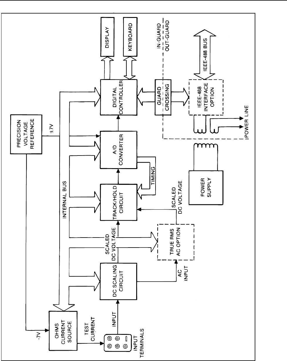
Theory of Operation
DC SCALING
5
5-5
f5-01.wmf
Figure 5-1. Overall Functional Block Diagram
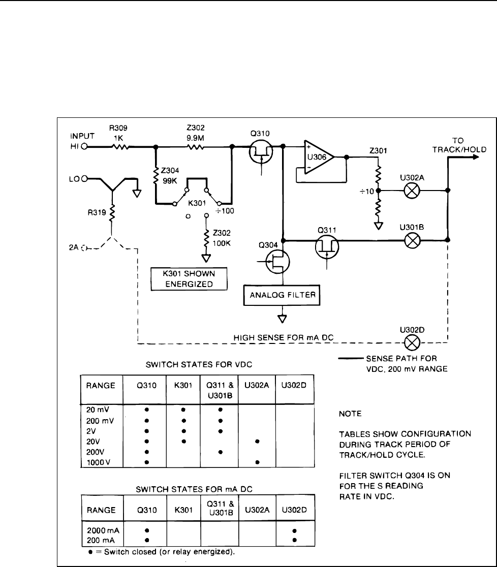
8842A
Instruction Manual
5-6
5-5. VDC Scaling
Scaling is performed in the VDC function by two precision resistors networks (Z301 and
Z302). These components are configured by relay K301, switching transistor Q311, and
quad analog switches U302A and U301B to provide the correct scaling for each range.
Voltage follower U306 provides high input impedance for the 20V dc range. A simplified
schematic and a switch state table for the VDC function are shown in Figure 5-2.
f5-02.wmf
Figure 5-2. DC Scaling (VDC and mA DC)

Theory of Operation
DC SCALING
5
5-7
In the 20 mV, 200 mV and and 2V ranges, the input voltage is applied directly to the T/H
Amplifier via Q310, Q311, and U301B. In the 20 mV range, the T/H Amplifier has a gain
of 100; in the 200 mV range, the T/H Amplifier has a gain of 10; in all other dc voltage
ranges, the T/H Amplifier has a gain of 1.
In the 20V range, the input voltage is buffered by unity-gain amplifier U306, and divided
by 10 by Z301. To allow U306 to handle +/-20V inputs, its power supplies are
"bootstrapped" by Q305 and Q306, so that the output voltage of U306 determines the
midpoint of its supply voltages. The positive supply is approximately 6.2V above the
input and the negative supply is approximately 6.2V below.
In the 200V and 1000V ranges, K301 is de-energized and the input voltage is divided by
100 by Z302. In the 200V range, the reduced input voltage is then applied directly to the
T/H Amplifier as in the 2V range. In the 1000V range, the reduced input voltage is
buffered by U306 and divided by 10 as in the 20V range.
5-6. VDC Protection
Input protection for the VDC function is provided by a 1K, fusible resistor (R309), four
metal-oxide varistors (MOVs) (RV301, RV402, RV403, and RV404), and additional
protection resistors and clamp circuits.
WARNING
TO AVOID INJURY OR EQUIPMENT DAMAGE, USE EXACT
REPLACEMENT PARTS FOR ALL PROTECTION COMPONENTS.
In all dc voltage ranges, voltage transients greater than 1560V are clamped by the MOVs.
Extreme overvoltage conditions cause R309 to fail open-circuit.
R309 is followed either by a 99 kΩ, 10W resistor network (Z304) in the 20 mV, 200 mV,
2V, and 20V ranges, or by 10 MΩ (Z302) to ground in the 200V and 1000V ranges. Z304
provides current limiting in extreme overvoltage conditions in the 20 mV, 200 mV, 2V,
and 20V ranges. The non-inverting input of U306 is clamped to +/-25V by Q307 and
Q308.
5-7. mA DC Scaling
In the mA DC function, the unknown current causes a voltage drop across current shunt
R319. This voltage drop is then measured as in the VDC function. The DC Scaling circuit
is configured as shown by the simplified switch table in Figure 5-2.
5-8. Analog Filter
The three-pole, low-pass analog filter (U304) has a Bessel response with corner
frequency at 7 Hz, giving approximately 50 dB of rejection at 50 Hz. The filter is used
for the slow reading rate and is used in the VDC ranges and lowest three ohms ranges.
The filter is also used in the 20mV DC, 20Ω, and 200 mA DC ranges when in the
medium reading rate. The filter is switched into the input signal path by Q304 (Figure 5-
2). In some ranges and functions, additional filtering is provided by Q317 and C314.
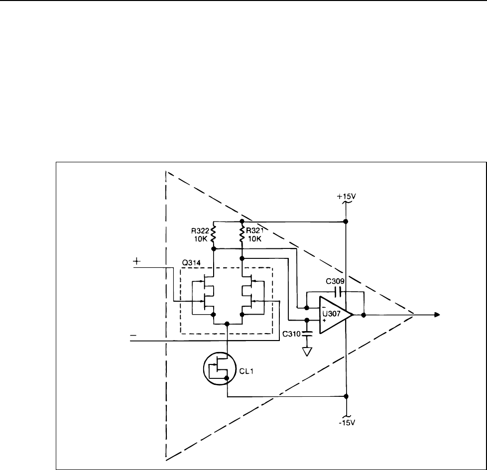
8842A
Instruction Manual
5-8
5-9. TRACK/HOLD CIRCUIT
The Track/Hold (T/H) circuit presents a stable voltage to the A/D Converter during the
input period of the A/D conversion cycle. The circuit also provides a gain of 100 in the
20 mV, 20Ω and 200 mA ranges, and a gain of 10 in the 200 mV dc, 200Ω, and 2000 mA
dc ranges.
The T/H circuit consists of the T/H Amplifier (Figure 5-3), T/H capacitor C308, quad
analog switches U301, U302, and U303, and associated components. As shown in Figure
5-3, the T/H Amplifier functions as an op amp, with Q314 supplying additional gain. In
subsequent figures, the T/H Amplifier is represented as a single op amp.
f5-03.wmf
Figure 5-3. Track/Hold Amplifier
The circuit operates by cycling between the track, settling, hold, and precharge
configurations shown in Figure 5-4. The In-Guard µC selects a particular settling and
hold configuration for each function and range, and suppresses the precharge
configuration for certain ranges. This control is achieved by latching function and range
information in U301, U302, and U303.
Basic timing for the T/H circuit is provided by the A/D Converter over clock lines PC,
HD1, TR1, and TR2. (See the timing diagram in Figure 5-5, top.) The T/H cycle is
initiated when the In-Guard µC pulls line TR low.
Theory of Operation
TRACK/HOLD CIRCUIT
5
5-9
f5-04.wmf
Figure 5-4. Track/Hold Circuit Configurations
8842A
Instruction Manual
5-10
f5-05.wmf
Figure 5-5. Timing Diagram for One A/D Cycle
5-10. Track Configuration
In the track configuration (Figure 5-4A), the T/H circuit functions as a non-inverting
buffer. The voltage on C308 tracks the scaled dc input voltage.
Theory of Operation
PRECISION VOLTAGE REFERENCE
5
5-11
5-11. Settling Configuration
The circuit assumes a settling configuration between the track and hold configurations.
The circuit assumes the configuration in Figure 5-4B for unity gain and the configuration
in Figure 5-4C for gain of 10.
During this time the DC Scaling circuit is still connected to the T/H amp. However,
changes in the input do not affect the value to be measured, which is stored on C308.
5-12. Hold Configuration
The X1 hold configuration (Figure 5-4D) is used for all VDC ranges except r1 and for all
ohms ranges except r1. The output of U307 is the negative of the input voltage.
The X10 hold configuration (Figure 5-4E) is used for the mA DC function, the 200 mV
dc range, and the 200Ω range, and provides a gain of 10.
5-13. Pre-Charge Configuration
The pre-charge configuration (Figure 5-4F) occurs after the hold configuration in VDC
ranges r1, r2, and r4, and ohms ranges r1, r2, r3, and r4. U306 is connected as a buffer to
charge stray capacitance at the non-inverting input of the T/H Amplifier. The pre-charge
configuration is not used in any other ranges.
5-14. PRECISION VOLTAGE REFERENCE
The Precision Voltage Reference (Figure 5-6) provides precise reference voltages of -
7.00000 and +7.00000. The reference element is a reference amplifier (ref amp). The
nominal ref amp voltage is 6.5V.
f5-06.wmf
Figure 5-6. Precision Voltage Reference
8842A
Instruction Manual
5-12
Resistor R701, precision resistor network Z701, and transistor/zener diode combination
U701 are produced as a matched set so that the output of U702A is precisely -7.00000V.
This output is remotely sensed at the pins of the custom A/D IC (U101). Diode CR701
prevents the output from going positive at power-up.
U702B functions as an inverter to provide the +7.00000V output and to supply the
reference amplifier. The gain of U702B is set by the two 20 kΩ resistors in the resistor
network Z702.
5-15. OHMS CURRENT SOURCE
The Ohms Current Source (Figure 5-7) provides a precise test current for the ohms
functions. The first stage (U401, R401, and Q401) produces a precise reference current,
using precision resistor R401 and a -7.0000V reference voltage from the Precision
Voltage Reference.
f5-07.wmf
Figure 5-7. Ohms Current Source

Theory of Operation
OHMS PROTECTION
5
5-13
The second stage (U404, precision resistor network Z401, and analog switches U402 and
U403) is a current amplifier whose gain is controlled by the In-Guard µC. The In-Guard
µC sets the output current for each range by controlling U402 and U403. (See switch
state table in Figure 5-7.)
5-16. OHMS PROTECTION
The Ohms Protection circuit (Q402, Q403, Q404, Q405, Q406, and Q407) clamps the
open circuit voltage of the Ohms Current Source and provides protection for the Ohms
Current Source.
The circuit protects the Ohms Current Source from up to +/-300V across the INPUT
terminals. The circuit also clamps voltage transients larger than 1560V with four MOVs
(RV401, RV402, RV403, and RV404). In addition, a 1 kΩ, 2W fusible wire-wound
resistor (R410) in series with the output current path fails open-circuit under extreme
overvoltage conditions.
Large positive input voltages are blocked by CR402. Large negative input voltages are
dropped equally across three high-voltage transistors (Q402, Q403, and Q404). If -300V
is present at the collector of Q404, the voltage drops equally across Z402 so that large
negative voltages never reach the current source.
The circuitry associated with Q408 (R406, R407, R408, R409, Q406, Q408, and CR403)
clamps the open-circuit voltage of the Ohms Current Source below +6.5V in the lower
four ranges and below +13V dc in the higher two ranges. The in-guard uC turns Q408 on
or off depending on range. In the lower four ohms ranges, Q408 is on, effectively
shorting R409; R406 and R409 then form a voltage divider which clamps the output of
the ohms current source below +6.5V. In the higher two ohms ranges, Q408 is off,
including R409 in the voltage divider and clamping the output below +13V.
5-17. OHMS FUNCTIONS
5-18. 2-Wire Ohms
In the 2-wire ohms function, the Ohms Current Source is connected to the INPUT HI
terminal by ohms relay K401 (Figure 5-8). The Ohms Current Source applies a known
current to the resistance under test, and the resulting voltage drop across the resistor is
measured ("sensed") as in the VDC function.
8842A
Instruction Manual
5-14
f5-08.wmf
Figure 5-8. Ohms Scaling

Theory of Operation
A/D CONVERTER
5
5-15
The voltage sensed at the INPUT terminals is scaled as shown by the simplified switch
table in Figure 5-8. (Refer to the track period of the track/hold cycle, during which the
scaled input voltage is sampled.)
In the lower five ranges, the full scale input voltage to the A/D Converter is 2V.
However, in the 2000 kΩ and 20 MΩ ranges, the full-scale input voltage to the A/D
Converter is +1V; the in-guard uC completes the scaling by multiplying the A/D result by
2.
5-19. 4-Wire Ohms
In the 4-wire ohms function, the Ohms Current Source is connected to the INPUT HI
terminal by ohms relay K401 as in 2-wire ohms (Figure 5-8). The Ohms Current Source
applies a known current to the resistance under test through the INPUT HI and INPUT
LO leads. The resulting voltage drop across the resistor is measured by the SENSE HI
and SENSE LO leads.
The voltage at the SENSE HI terminal is connected to the DC Scaling circuit by Q303
(Figure 5-8). The voltage is then scaled exactly as in the 2-wire ohms function. (Refer to
the track period in the switch table in Figure 5-8.) Q310 is turned off to isolate the
SENSE HI terminal from the INPUT HI terminal.
Additional input switching occurs during the hold period of the track/hold cycle. (Refer
to the hold period in the switch table in Figure 5-8.) In ranges r1 through r4, and r8, the
SENSE LO terminal is switched into the dc input path by U301D, and the INPUT LO
terminal is switched out of the dc input path by U301C. This has the effect of measuring
the SENSE HI terminal with respect to the SENSE LO terminal.
In ranges r5 and r6, the SENSE LO and INPUT LO terminals are both switched into the
dc input path by U301C and U301D during the hold period. This has the effect of
measuring the SENSE HI terminal with respect to INPUT LO terminal rather than
SENSE LO. Although the resistance of the INPUT LO lead is in series with the unknown
resistance, accuracy is not affected as long as the resistance of the lead is less than 10Ω in
the 2000 kΩ range and less than 100Ω in the 20 MΩ range.
5-20. A/D CONVERTER
The Analog-to-Digital (A/D) Converter (Figure 5-9) uses Fluke’s patented recirculating
remainder technique. An input voltage (Vin) is compared to the output of the precision
Digital-to-Analog Converter (DAC). The output of the A/D Amplifier, connected as a
comparator, is monitored to indicate when the DAC output is larger than the input
voltage.
8842A
Instruction Manual
5-16
f5-09.wmf
Figure 5-9. Analog-to-Digital Converter
The conversion process is broken up into an autozero period followed by five
measurement intervals. (A timing diagram is shown in Figure 5-5.) Six bits of the final
A/D sample are obtained during each interval.
During the first compare period (shown in Figure 5-9), the A/D Converter determines the
value of the scaled input voltage (Vin) by comparing Vin to the output of the DAC. Each
of the DAC bit-switches is tried in sequence and kept or rejected (left closed or reopened)
depending on the output polarity of the A/D Amplifier, which is configured as a
comparator. This process produces a string of six bits which is stored in the Timing/Data
Control circuit (the digital portion of U101).
During the following remainder-store period (Figure 5-10), the difference between the
Vin and the DAC output is multiplied by 16 by the A/D Amplifier and stored on
capacitor C102. During subsequent compare and remainder-store periods, the remainder
voltage is connected to the input of U103 and is resolved to six bits; the remainder
voltage (multiplied by 16) is stored alternately on capacitor C102 and C103. Each of the
five compare periods thus produces a six-bit nibble which is stored in the Timing/Data
Control circuit.
Theory of Operation
A/D CONVERTER
5
5-17
f5-10.wmf
Figure 5-10. First Remainder-Store Period
This five-interval process thus generates five nibbles which are processed by the In-
Guard µC to produce one A/D sample. After the fifth nibble is generated, U101 interrupts
the In-Guard µC over line INT. The In-Guard µC then pulls line CS7 low five times,
causing U101 to send the µC the five (six-bit) nibbles one-at-a-time over lines AD0-
AD5. The In-Guard µC then weights each nibble 1/16 of the value of the previous
number and calculates the input voltage.
The hardware for the A/D Converter has four major sections: Timing/Data Control,
Precision DAC, A/D Amplifier, and bootstrap supplies.
5-21. Timing/Data Control
The Timing/Data Control circuit (the digital portion of U101) times and controls the A/D
Converter by manipulating the switches in the A/D Amplifier and the bit-switches in the
Precision DAC. An A/D conversion cycle is triggered by the falling edge of line TR from
the In-Guard µC. Once triggered, the A/D Converter (under control by U101) generates
the five 6-bit nibbles without further interaction with the In-Guard µC.
The Timing/Data Control circuit also provides a watch-dog timer (line RES not) which
resets the In-Guard µC in case normal program execution is interrupted. If the timer
senses inactivity on line CS7 for longer than 1.5 seconds, it resets the In-Guard µC by
pulling RES not low.
The Timing/Data Control circuit is supplied with a fixed-rate 8 MHz clock and provides a
1 MHz output clock for the Keyboard/Display Interface (U212). In addition, four output
lines (PC, HD1 not) TR1, and TR2) provide control signals for the Track/Hold circuit.
5-22. Precision DAC
The Precision Digital-to-Analog Converter (DAC) is composed of DAC Amplifier
U102B and a binary ladder network, which consists of resistors in Z101 and digitally
controlled analog bit-switches contained in U101.
8842A
Instruction Manual
5-18
The bit-switches determine the output voltage of U102B by controlling the binary ladder
network. The gain of U102B is set by the ratio of a precision feedback resistor (Z101-7, -
8) and the equivalent output resistance of the ladder network.
5-23. A/D Amplifier
The A/D Amplifier is composed of a comparator/amplifier (U103), two remainder-
storage capacitors (C103 and C102), an autozero storage capacitor (C101), and several
digitally controlled analog switches contained in U101.
The A/D Amplifier has three modes of operation: autozero mode, where any offsets in
the A/D input are stored on C101 so as to be cancelled later; compare mode, where the
A/D input is compared to the DAC output; and remainder-store mode, where U103
amplifies and stores the difference between the A/D input and the DAC output on one of
the two remainder-storage capacitors (C102 or C103). The autozero mode is shown in
Figure 5-11. The other modes are shown in Figures 5-9 and 5-10.
f5-11.wmf
Figure 5-11. Autozero Period
5-24. Bootstrap Supplies
The bootstrap supplies are composed of U102A, Q101, Q102, CR103, CR104, and
associated components. The bootstrap supplies enhance the gain accuracy of U103.
During compare periods, the bootstrap supplies limit the output of U103 to minimize the
time it takes to recover from being driven to a supply rail. Both functions are achieved by
manipulating the supplies of U103 (BS1 and BS2).
5-25. DISPLAY
The vacuum fluorescent display is similar to a vacuum tube, containing eight control
grids and 69 phosphor-coated plates which form the display segments and annunciators.
(See Figure 5-12.) The filament voltage is 4.5V ac, with a +5V dc bias. Each plate is
controlled by a G line and a P line. The G lines go to the control grids, and the P lines go
to the plates.
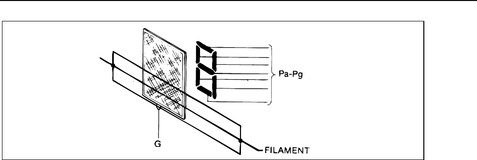
Theory of Operation
KEYBOARD
5
5-19
f5-12.wmf
Figure 5-12. Vacuum Fluorescent Display
The Digital Controller sequentially enables the G lines by applying +30V dc (nominal).
When a G line is enabled, electrons flow from the filament to the enabled grid. If a P line
is enabled (i.e., raised to a nominal +30V dc by the Digital Controller), the electrons
continue past the grid and strike the respective plate, causing it to glow.
5-26. KEYBOARD
The keyboard consists of a silicone-rubber switch matrix located over metalized epoxy
contacts on the printed wire board. Each button contains a conductive pad that shorts two
contacts when pressed.
5-27. DIGITAL CONTROLLER
The Digital Controller (Figure 5-13) consists of the In-Guard µC (U202), External
Program Memory (U222), Calibration Memory (U220), Keyboard/Display Interface, and
associated components.
8842A
Instruction Manual
5-20
f5-13.wmf
Figure 5-13. Digital Controller Block Diagram

Theory of Operation
DIGITAL CONTROLLER
5
5-21
5-28. In-Guard Microcomputer
The In-Guard Microcomputer (µC) is a single-chip Z8 microcomputer containing 4K
bytes of ROM, 144 bytes of RAM, a UART, and four 8-bit I/O ports. It communicates
with the rest of the instrument via the internal bus and dedicated I/O lines. The In-Guard
µC is reset when pin 6 is pulled low either by C204 at power-up or by the watch-dog
timer in the custom A/D IC (U101). Pin 6 is tied to +5V through a 100 kΩ resistor inside
the µC.
All internal bus communication is memory-mapped. Each component that sends or
receives data on the bus has a unique address or range of addresses. The internal bus
consists of lines AD0-AD7 and A8-A11. Lines AD0-AD7 are time-multiplexed to carry
both the least-significant address byte and the data. Lines A8-A11 carry the most-
significant bits of the address. The µC writes to and reads from the internal bus according
to the read and write cycles shown in Figure 5-14. During either cycle, the address strobe
(AS) changes from low to high when an address is valid, and the data strobe (DS)
changes from low to high when the data is valid.
The address strobe latches the address on AD0-AD7 into U219 which then provides static
address inputs for those devices that need it while data is on the bus. The data memory
line (DM) divides the address space between program memory (U222) and data memory
(all other devices on the bus). The data memory address space is further divided between
the calibration memory (U220) and the remaining devices by A11. The addresses of the
remaining devices are decoded from A8-A10 by U208, which combines the address with
the data strobe (DS) to provide a chip select (CS0, CS2, CS3, CS4, or CS7) for each
device.
The In-Guard µC performs the following functions: range and function control; A/D
control and computation; calibration corrections; keyboard/display control; serial
communication with the IEEE-488 Interface; and diagnostic self-testing and
troubleshooting.
8842A
Instruction Manual
5-22
f5-14.wmf
Figure 5-14. Read/Write Timing Diagrams for Internal Bus

Theory of Operation
DIGITAL CONTROLLER
5
5-23
5-29. Function and Range Control
The In-Guard µC configures the DC Scaling circuit, the Track/Hold circuit, and the
Ohms Current Source to provide the proper input switching, scaling, and filtering for
each function, range, and reading rate. It does this by controlling dedicated output lines
which control relays and FET switches, and by sending configuration codes out on the
bus. The quad analog switches (U301, U302, U303, U402, and U403) latch the
configuration codes and perform any level-shifting needed to control their internal
MOSFET switches. Some of the switches require dynamic timing signals from the
custom A/D IC (U101); these signals are combined appropriately in the quad analog
switches with the configuration codes.
5-30. A/D Control and Computation
The In-Guard µC initiates each A/D sample by pulling line TR low. When the µC is
reset, it senses the power line frequency on line FREQ REF. The µC then sets its internal
timer so that the A/D sample rate is as shown in Table 5-1.
The number of readings per second for the slow and medium rates are chosen to provide
rejection of input signals that are at the line frequencies.
Table 5-1. Sample Rates and Reading Rates
SLOW MEDIUM FAST
POWER LINE
FREQUENCY Samples
per Sec
Samples
per
Reading
Samples
per Sec
Samples
per
Reading
Samples
per Sec
Samples
per
Reading
50 Hz 66.67 32 66.67 4 100 1
60 Hz 80 32 80 4 100 1
400 Hz 76.19 32 76.19 4 100 1
The custom A/D IC (U101) generates five 6-bit numbers after each trigger from the µC
and then pulls INT low, telling the µC that data is ready. The µC reads the five 6-bit
numbers over the bus (CS7 pulses low five times for five read cycles) and computes the
value of the A/D sample using calibration constants. The µC averages the appropriate
number of samples for one reading, which is then sent to the keyboard/display interface
for display.
For example, with a 60-Hz power-line frequency, an externally triggered reading in the
slow reading rate would cause the µC to send 32 pulses on TR at an 80 Hz rate. The 32
A/D samples would be calibrated and averaged by the µC and sent for display. With
internal triggering, the A/D runs continuously at 80 samples per second with a reading
being sent to the display every 32 samples.
5-31. Calibration Correction
The calibration constants used by the In-Guard µC in computing each reading are stored
in the EEROM (electronically erasable read-only memory) Calibration Memory (U220).
The front panel CAL ENABLE switch protects the EEROM from accidental writes.
8842A
Instruction Manual
5-24
5-32. Keyboard/Display Control
Keyboard/Display Controller U212 communicates with the In-Guard µC over the internal
bus. During a µC write cycle, address line A0 tells U212 whether to consider data being
sent by the µC as configuration commands or as display data. Display data is stored in the
Keyboard/Display Controller, which automatically scans the display. The
Keyboard/Display Controller selects one of eight grids using decoder U213 and buffer
U215. The numeric display data is decoded from BCD to 7-segment by decoder U216
and buffered by U217. Additional annunciator data is buffered by U218.
The Keyboard/Display Controller is reset by the µC whenever the µC is reset. It receives
a 1-MHz clock signal from the custom A/D IC (U101), which uses the µC 8-MHz crystal
for its clock input.
The Keyboard/Display Controller scans the keyboard, sensing pressed buttons on lines
RL0-RL7. It sends an interrupt to the µC via line KEYINT whenever a front panel button
is pressed. The µC then reads the keycode from the Keyboard/Display Controller. (The
status of the FRONT/REAR switch is sensed separately by line F/R SENSE.)
5-33. Troubleshooting Modes
In addition to running the diagnostic self-tests, the In-Guard µC has a troubleshooting
mode which aids in finding digital hardware problems. After the uC is reset, it senses the
relay control lines (U202-35 through U202-38) as inputs. If line U202-38 (TP205) is
shorted to ground, the µC goes into the troubleshooting mode. (U201 provides internal
pull-up.) The troubleshooting mode is described in detail in the Maintenance section.
5-34. Guard-Crossing Communication
The In-Guard µC contains a UART (universal asynchronous receiver transmitter) which
it uses to communicate across the guard to the IEEE-488 Interface. The transmission
speed is 62,500 bits per second.
5-35. GUARD CROSSING
The Guard Crossing consists of two identical circuits, each of which transmits data in one
direction across the guard isolation between the Main Printed Circuit Assembly and the
IEEE-488 Interface. One circuit is shown in Figure 5-15; the other circuit works
identically. A portion of each circuit is contained in the IEEE-488 Interface.
f5-15.wmf
Figure 5-15. Guard Crossing Circuit

Theory of Operation
POWER SUPPLY
5
5-25
The circuit in Figure 5-15 has two stable states, corresponding to output high (+5V) and
output low (0V). If the output is high, the voltage present at the non-inverting input of op
amp A is approximately +140 mV.
Since the inputs to op amps A and B are inverted, their outputs are always in opposite
states. If the output of A is high, the output of B is low, forcing the inverting input of A
(and the non-inverting input of B) to ground, hence reinforcing the existing state. The
situation is analogous if the output of A is low.
A positive-going transition at the input causes a positive pulse at the non-inverting input
of A, and a corresponding negative pulse at the inverting input of A. If the output is high
to start with (with the non-inverting input of A raised 140 mV above its inverting input),
these pulses reinforce the existing state (raising the non-inverting input and lowering the
inverting input). If, however, the output is low to start with, the positive pulse (which is
greater than 140 mV) raises the non-inverting input of A above its inverting input,
switching the output to the high state. The situation is analogous for a negative-going
input transition.
5-36. POWER SUPPLY
The Power Supply provides the following in-guard outputs: +/-30V, +/-15V, -6.2V,
+7.5V, +5V, -5V, and -8.2V dc; and 4.5V ac. The Power Supply also provides a 16V ac
center-tapped out-guard output.
Input line voltage is directed to the primary transformer winding through fuse F601, the
front panel POWER switch, and the rear panel LINE SET switches. Metal oxide varistor
RV601 clamps line transients at about 390V. The LINE SET switches configure the
Power Supply to accept line power of 100, 120, 220, or 240V ac (+/-10% with a
maximum of 250V) at 50, 60, or 400 Hz.
AC voltage for the +5V supply is rectified by CR601 and CR602 and regulated by
VR601. The +5V output supplies mostly logic circuits. The ac input to the +5V supply is
sensed by the In-Guard µC (via R604, CR615, and U221-12, 13) to measure the line
frequency.
AC voltage for the +30V and -30V supplies is rectified by bridge network CR603,
CR604, CR605, and CR606 and regulated by VR602 and VR605. The +30V and -30V
outputs supply front-end buffer amp U306. In addition, the +30V output supplies the
anodes of the vacuum fluorescent display. Zener diode CR612 supplies -6.2V to the A/D
Converter clamps.
AC voltage for the +15V and -15V supplies is rectified by bridge network CR608,
CR609, CR610, and CR611 and regulated by VR603 and VR604. The +15V and -15V
supply analog circuitry throughout the 8842A. Zener diodes CR613 and CR614 supply
+7.5V and -8.2V to the A/D Converter, analog filter, and DC Scaling circuit.
Secondary T601-14, 15, 16 supplies the vacuum fluorescent display filament with 4.5V
ac. The center tap is connected to the in-guard +5V supply in order to correctly bias the
display. An isolated secondary supplies 16V ac to the power supply on the IEEE-488
Interface.
Zener diode CR615 and SCR Q601 comprise a protective crow-bar circuit. If the line
voltage exceeds the nominal value by approximately 30 percent or more, CR615
conducts, turning on Q601, shorting out the power transformer secondary and blowing
the line fuse. In normal operation, these components have no effect.
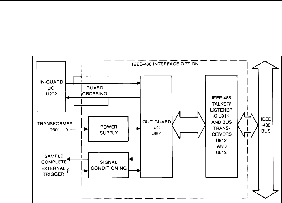
8842A
Instruction Manual
5-26
5-37. IEEE-488 INTERFACE (OPTION -05)
The IEEE-488 Interface has five major parts, as shown in the block diagram in Figure 5-
16. All components are contained in a single printed circuit assembly (PCA). Reference
designations are numbered in the 900 series.
f5-16.wmf
Figure 5-16. IEEE-488 Interface Block Diagram
5-38. Out-Guard Microcomputer
The Out-Guard Microcomputer (µC) (U901) communicates with the IEEE-488
talker/listener IC (U911) and the In-Guard µC (U202).
The Out-Guard µC is similar to the In-Guard Z8 µC except that is contains 8K bytes of
ROM and 236 bytes of RAM. For futher description of the Z8 µC, refer to the heading
"In-Guard Microcimputer, " above.
5-39. Guard Crossing
The guard crossing circuit permits serial asynchronous communication between U901
and U202 while isolating the two electrically. One-half of the guard crossing circuit is
contained on the Main PCA; the other half is on the IEEE-488 Interface PCA. Operation
of the guard crossing circuit is described in an earlier heading.
5-40. Bus Interface Circuitry
The IEEE-488 bus protocol is handled by the uPD7210 IEEE-488 talker/listener IC
(U911). It is controlled by U901 as a memory mapped peripheral through an 8-bit data
bus.
Bus transceivers U912 and U913 buffer U911 from the IEEE-488 bus. They provide the
bus with the required output drive capability and receiver impedance.
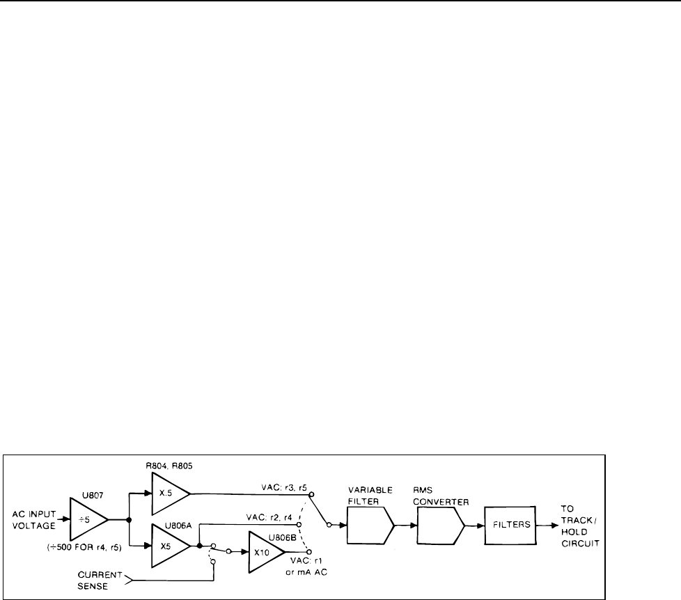
Theory of Operation
TRUE RMS AC (OPTION -09)
5
5-27
5-41. Signal Conditioning
The SAMPLE COMPLETE and EXT TRIG signals (J903 and J904) are conditioned by
U909. Diodes CR903, CR904, CR905, and CR906 and resistors R917 and R918 provide
protection from excessive voltages. Jumpers E902 and E903 allow selection of the
polarity of the EXT TRIG signal. (A polarity selection procedure is given in the
Maintenance section.) The 8842A is configured in the factory so that it is triggered on the
falling edge of the EXT TRIG signal.
5-42. IEEE-488 Interface Power Supply
The IEEE-488 Interface power supply circuit provides the IEEE-488 Interface PCA with
+5V. The circuit consists of rectifying diodes CR908 and CR909, filter capacitor C910,
and voltage regulator VR901. Power comes from transformer T605 on the Main PCA.
U908 and associated circuitry resets the Out-Guard µC at power-up and following power-
line voltage dropouts.
5-43. TRUE RMS AC (OPTION -09)
The True RMS AC circuit (Figure 5-17) performs two primary functions. First, it scales
ac input voltages and ac current sense voltages to a range of 0V to 2V ac rms. Second, it
converts the scaled ac voltages to an equivalent dc voltage which is then directed to the
A/D Converter via the Track/Hold Amplifier. The True RMS AC circuit is trimmed for
flat high-frequency response using a variable filter which is set by the High-Frequency
AC Calibration procedure.
f5-17.wmf
Figure 5-17. True RMS AC Option Block Diagram
The following paragraphs describe how these functions are performed. Components are
laid out on a single printed circuit assembly (PCA). Component reference designators are
numbered in the 800 series.
5-44. VAC Scaling
AC voltage inputs are directed from the HI INPUT terminal to the True RMS AC PCA
through protection resistor R309 on the Main PCA. In this way, voltage transients greater
than 1560V are clamped by MOVs (RV301, RV402, RV403, and RV404) as in the VDC
function. With the VAC function selected, K801 is closed. The input voltage is thus
applied to C801, which blocks dc inputs.
U807 and resistor network Z801 provide selectable attenuation and 1 MΩ input
impedance. In the upper two ranges, K802 is closed and Q806 is off, providing a gain of -
1/500. In the lower three ranges, K802 is open and Q806 is on, shorting Z801-4 to
ground; this configuration provides a gain of -1/5. CR801 and CR802 provide protection
by clamping the inverting input of U807 to approximately +/-0.6V. Q805 shifts logic
levels to control Q806.
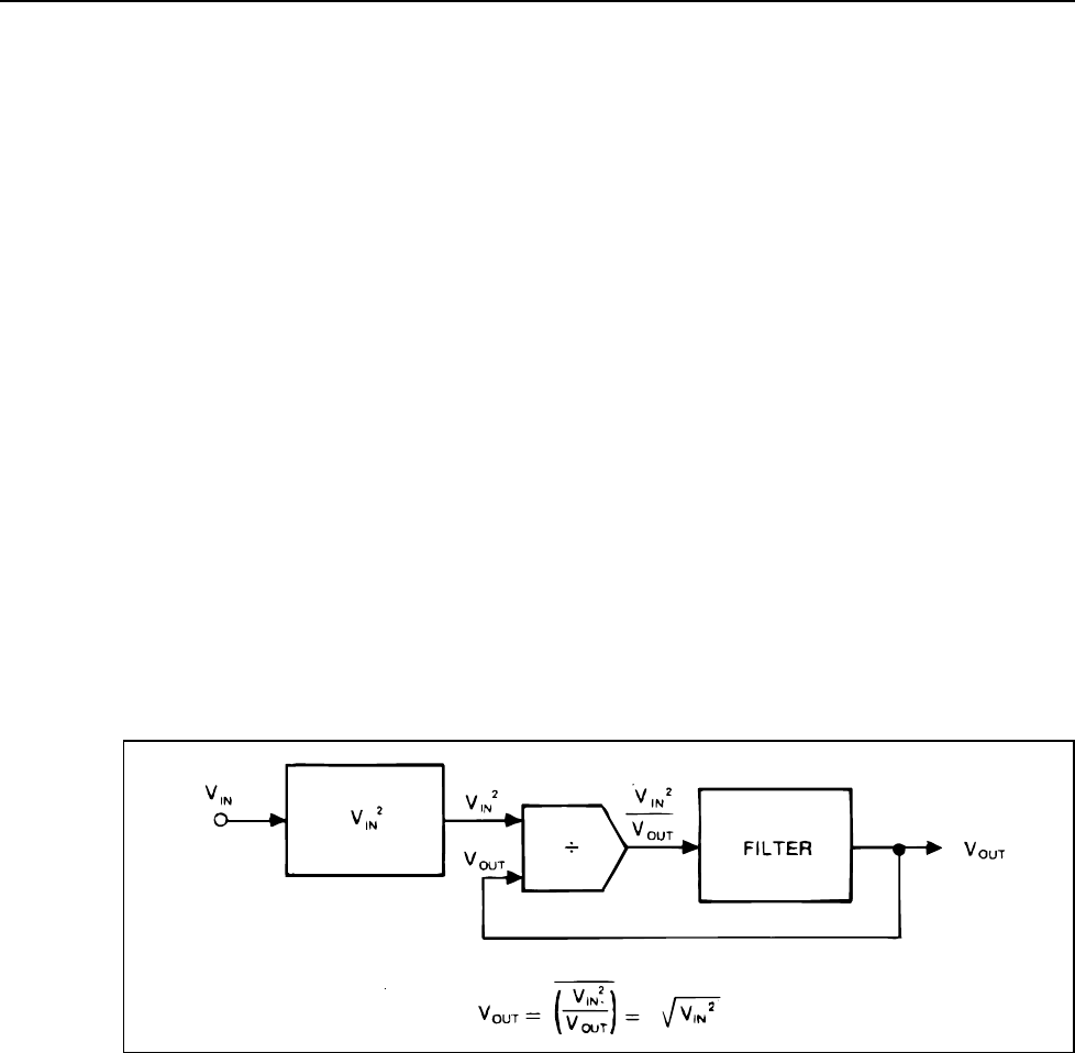
8842A
Instruction Manual
5-28
U806A, U806B, and a voltage divider (R804 and R805) provide gain which is selected
for each range by the analog switches in U804. The configuration for each range is shown
in Figure 5-17. (In this figure, the CMOS analog switches are represented by mechanical
switches.) When U806A is not used, its non-inverting input is grounded by Q804. When
U806B is not used, its non-inverting input is connected to the CURRENT SENSE line.
5-45. mA AC Scaling
The mA AC function uses the same current shunt and protection network which is used
for dc current. In the mA AC function, Q802 switches the CURRENT SENSE line to the
non-inverting input of U806B, which provides a gain of 10.
5-46. Frequency Response Trimming
The frequency response is trimmed by software calibration using a digitally controlled
one-pole low-pass filter (R832 and a combination of C826, C827, C828, and C829). The
analog switches in U808 configure the four capacitors to select one of 16 possible RC
constants. The input of the digitally controlled filter is buffered by voltage follower
U801A. The individual gain stages are also provided with fixed frequency compensation.
5-47. True RMS AC-to-DC Conversion
U801B buffers the input to rms converter U802. U802 computes the rms value of the
scaled input voltage as shown in Figure 5-18. Rather than explicitly squaring and
averaging the input, U802 uses an implicit method in which feedback is used to perform
an equivalent analog computation.
f5-18.wmf
Figure 5-18. True RMS AC-to-DC Converter
The filter averages the divider output signal. This filter consists of U809A, C813, R815,
and the internal 25 kΩ resistor and op amp between pins 8 and 9 of U802. The output is
further filtered by a three-pole post-filter comprised of U809B and associated resistors
and capacitors. This output is then switched into the Track/Hold Amplifier of the dc front
end via U302 pins 15 and 14. The Track/Hold Amplifier is set up for unity gain on all ac
ranges.
Some semiconductors and custom IC's can be
damaged by electrostatic discharge during
handling. This notice explains how you can
minimize the chances of destroying such devices
by:
1. Knowing that there is a problem.
2. Leaning the guidelines for handling them.
3. Using the procedures, packaging, and
bench techniques that are recommended.
The following practices should be followed to minimize damage to S.S. (static sensitive) devices.
1. MINIMIZE HANDLING
2. KEEP PARTS IN ORIGINAL CONTAINERS
UNTIL READY FOR USE.
3. DISCHARGE PERSONAL STATIC BEFORE
HANDLING DEVICES. USE A HIGH RESIS-
TANCE GROUNDING WRIST STRAP.
4. HANDLE S.S. DEVICES BY THE BODY.
static awareness
A Message From
Fluke Corporation
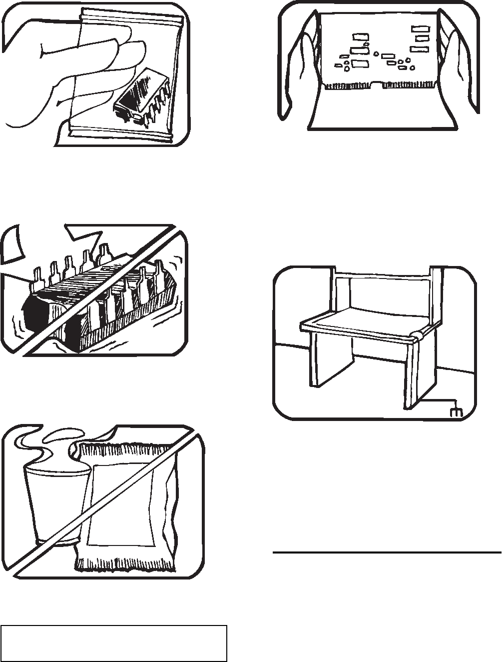
5. USE STATIC SHIELDING CONTAINERS FOR
HANDLING AND TRANSPORT.
6. DO NOT SLIDE S.S. DEVICES OVER
ANY SURFACE.
7. AVOID PLASTIC,VINYL AND STYROFOAM
IN WORK AREA.
8. WHEN REMOVING PLUG-IN ASSEMBLIES
HANDLE ONLY BY NON-CONDUCTIVE
EDGES AND NEVER TOUCH OPEN EDGE
CONNECTOR EXCEPT AT STATIC-FREE
WORK STATION. PLACING SHORTING
STRIPS ON EDGE CONNECTOR HELPS
PROTECT INSTALLED S.S. DEVICES.
9. HANDLE S.S. DEVICES ONLY AT A
STATIC-FREE WORK STATION.
10. ONLY ANTI-STATIC TYPE SOLDER-
SUCKERS SHOULD BE USED.
11. ONLY GROUNDED-TIP SOLDERING
IRONS SHOULD BE USED.
PORTIONS REPRINTED
WITH PERMISSION FROM TEKTRONIX INC.
AND GERNER DYNAMICS, POMONA DIV.
Dow Chemical
6-1
Chapter 6
Maintenance
Title Page
6-1. INTRODUCTION.................................................................................. 6-3
6-2. PERFORMANCE TEST........................................................................ 6-4
6-3. Diagnostic Self-Tests ......................................................................... 6-4
6-4. DC Voltage Test................................................................................. 6-5
6-5. AC Voltage Test (Option -09 Only)................................................... 6-7
6-6. Resistance Test................................................................................... 6-8
6-7. DC Current Test................................................................................. 6-9
6-8. AC Current Test (Option -09 Only)................................................... 6-10
6-9. CALIBRATION..................................................................................... 6-10
6-10. Basic Calibration Procedure............................................................... 6-11
6-11. INITIAL PROCEDURE................................................................ 6-11
6-12. A/D CALIBRATION .................................................................... 6-12
6-13. OFFSET AND GAIN CALIBRATION ........................................ 6-14
6-14. HIGH-FREQUENCY AC CALIBRATION.................................. 6-15
6-15. Advanced Features and Special Considerations................................. 6-16
6-16. STORING VARIABLE INPUTS.................................................. 6-16
6-17. CALIBRATING INDIVIDUAL RANGES................................... 6-17
6-18. VERIFYING CALIBRATION...................................................... 6-17
6-19. ERASING CALIBRATION MEMORY....................................... 6-18
6-20. TOLERANCE CHECK ................................................................. 6-18
6-21. AC CALIBRATION AT OTHER FREQUENCIES ..................... 6-19
6-22. OPTIMIZING USE OF THE 5450A............................................. 6-19
6-23. Remote Calibration ............................................................................ 6-20
6-24. TIMING CONSIDERATIONS ..................................................... 6-23
6-25. REMOTE ERASURE.................................................................... 6-24
6-26. EXAMPLE CALIBRATION PROGRAM.................................... 6-24
6-27. DISASSEMBLY PROCEDURE............................................................ 6-25
6-28. Case Removal..................................................................................... 6-26
6-29. True RMS AC PCA Removal (Option -09 Only).............................. 6-30
6-30. IEEE-488 Interface PCA Removal (Option -05 Only) ...................... 6-30
6-31. Main PCA Removal........................................................................... 6-30
6-32. Front Panel Disassembly.................................................................... 6-32
6-33. REASSEMBLY PROCEDURE............................................................. 6-32
6-34. INTERNAL FUSE REPLACEMENT ................................................... 6-36

8842A
Instruction Manual
6-2
6-35. EXTERNAL TRIGGER POLARITY SELECTION (Option -05 Only) 6-36
6-36. TROUBLESHOOTING ......................................................................... 6-36
6-37. Initial Troubleshooting Procedure...................................................... 6-36
6-38. Diagnostic Self-Tests ......................................................................... 6-41
6-39. Self-Test Descriptions........................................................................ 6-42
6-40. Digital Controller Troubleshooting.................................................... 6-45
6-41. IN-GUARD MICROCOMPUTER SYSTEM............................... 6-45
6-48. DISPLAY SYSTEM...................................................................... 6-48
6-59. ANALOG CONTROL SIGNALS................................................. 6-51
6-62. DC Scaling Troubleshooting.............................................................. 6-54
6-63. Track/Hold Troubleshooting.............................................................. 6-56
6-64. Ohms Current Source Troubleshooting.............................................. 6-56
6-65. Precision Voltage Reference Troubleshooting................................... 6-58
6-66. A/D Converter Troubleshooting......................................................... 6-59
6-67. Power Supply Troubleshooting.......................................................... 6-61
6-68. IEEE-488 Interface Troubleshooting (Option -05) ............................ 6-64
6-69. SERVICE POSITION.................................................................... 6-64
6-70. DIAGNOSTIC PROGRAM .......................................................... 6-64
6-71. True RMS AC Troubleshooting (Option -09).................................... 6-66
6-72. SERVICE POSITION.................................................................... 6-66
6-73. MAJOR PROBLEMS.................................................................... 6-67
6-74. MORE OBSCURE PROBLEMS .................................................. 6-69
6-75. Guard Crossing Troubleshooting....................................................... 6-70
6-76. INTERNAL CLEANING....................................................................... 6-70
6-77. Cleaning Printed Circuit Assemblies ................................................. 6-70
6-78. Cleaning After Soldering ................................................................... 6-71
Maintenance
INTRODUCTION
6
6-3
WARNING
THESE SERVICE INSTRUCTIONS ARE FOR USE BY QUALIFIED
PERSONNEL ONLY. TO AVOID ELECTRIC SHOCK, DO NOT
PERFORM ANY PROCEDURES IN THIS SECTION UNLESS YOU
ARE QUALIFIED TO DO SO.
6-1. INTRODUCTION
This section presents maintenance information for the 8842A. The section includes a
performance test, a calibration procedure, troubleshooting information, and other general
service information.
Test equipment recommended for the performance test and calibration procedure is listed
in Table 6-1. If the recommended equipment is not available, equipment that meets the
indicated minimum specifications may be substituted.
Table 6-1. Recommended Test Equipment
INSTRUMENT
TYPE
MINIMUM SPECIFICATIONS RECOMMENDED MODEL
PREFERRED:
Voltage Range: 0-1000V dc
Voltage Accuracy: 10 ppm
Absolute Linearity: ±1.0 ppm
Fluke 5700A or Fluke 5440A
ALTERNATIVE:
(Must be used with Kelvin-
Varley Voltage Divider)
Voltage Range: 0-1000V dc
Voltage Accuracy: 20 ppm + 20 ppm
of range
Fluke 720A
DC Calibrator
Kelvin-Varley Voltage Divider:
Ratio Range: 0-1.0
Absolute Linearity: ± 1 ppm of input
at dial setting
Fluke 720A
Resistor Calibrator Resistance Accuracy: 0.0005% Fluke 5700A or Fluke 5450A, ESI
DB62
DC Current Source Accuracy: ±0.025% Fluke 5700A or Fluke 5100B
Oscilloscope General porpose, 60 MHz, with 10
MΩ probe Philips PM3055 or PM3355
Digital Multimeter Voltage Accuracy
:0.01% in V dc
1.0% for 1V in V ac @ 100 kHz
Input Impedance:
10 MΩ or greater in V dc;
1 MΩ or greater in parallel with <100
pF in V ac
Fluke 8842A (with AC Option –09)
8842A
Instruction Manual
6-4
AC Calibrator Fluke 5700A and Fluke 5725A
Minimum Required Accuracy (By Range)
Frequency Range 1, 10, 100 mV11, 10, 100V21000V2
20 Hz – 30 Hz .1 + .005 .1 + .005 .12 + .005
30 Hz – 20 kHz .02 + 10 0.2 + .002 .04 + .004
20 kHz – 50 kHz .05 + 20 .05 + .005 .08 + .005
50 kHz – 100 kHz .05 + 20 .05 + .005 .1 + .01
1. ±(% of setting + µV) 2. +/-(% of setting + % of range)
AC Current Source Fluke 5700A
Frequency Range Minimum Required Accuracy (All Ranges)
30 Hz – 1 kHz ±.07% + 1 mA)
1kHz – 5 kHz ±(.07% + 1 mA) X frequency in kHz
Shorting Bar Resistance <1.5 mΩ
Construction Soldered (not
rivetted)
Pomona MDP-S-0
6-Inch Jumper ---- E-Z-Hook 204-6W-S or equivalent
Optional Test
Equipment 9010A, 9005A or Micro-System Troubleshooter; 9000A-8048 Interface Pod.
6-2. PERFORMANCE TEST
This test compares the performance of the 8842A with the specifications given in Section
1. The test is recommended as an acceptance test when the instrument is first received,
and as a verification test after performing the calibration procedure. If the instrument
does not meet the performance test, calibration or repair is needed.
To ensure optimum performance, the test must be performed at an ambient temperature
of 18°C to 28°C, with a relative humidity of less than 75%. Also, the 8842A should be
allowed to warm up for one hour prior to beginning any test other than the self-test.
6-3. Diagnostic Self-Tests
The diagnostic self-tests check the analog and digital circuitry in the 8842A. There are 21
analog tests followed by in-guard program memory, calibration memory, and display
tests. Out-guard program memory is tested when self-test is initiated by a remote
command. Microcomputer RAM tests are done only at powerup. Each test is described
in detail under the heading Troubleshooting. All five digital tests are performed at
powerup.
NOTE
The inputs must be left open-circuited while the self-tests are performed.
Otherwise, the 8842A may indicate errors are present. Errors may also be
caused by inductive or capacitive pick-up from long test leads.
If the FRONT/REAR switch is in the REAR position, the 8842A skips tests 3
and 4. Also, if Option -09 is not installed, the 8842A skips tests 1, 2, and 3.

Maintenance
PERFORMANCE TEST
6
6-5
To initiate the self-tests, press the SRQ button for 3 seconds. The TEST annunciator will
then light up, and the 8842A will run through the analog tests in sequence. Each test
number is displayed for about 1 second. The instrument can be stopped in any of the test
configurations by pressing the SRQ button while the test number is displayed. Pressing
any button continues the tests.
After the last analog test is performed, all display segments light up while the instrument
performs the in-guard program memory, calibration memory, and display tests. The
instrument then assumes the power-up configuration: VDC, autorange, slow reading rate,
offset off, local control.
If the 8842A detects an error during one of the tests, it displays the ERROR annunciator
and the test number for about 2-1/2 seconds, and then proceeds to the next test. The test
number thus becomes an error code. (Error codes are listed in Table 2-1, Section 2.)
Passing all diagnostic self-tests does not necessarily mean the 8842A is 100% functional.
The test, for example, cannot check the accuracy of the analog circuitry. If one or more
errors are displayed, the 8842A probably requires service.
6-4. DC Voltage Test
The following procedure may be used to verify the accuracy of the VDC function:
1. Ensure the 8842A is on and has warmed up for at least 1 hour.
2. Select the VDC function.
3. Connect the DC Calibrator (see Table 6-1) to provide a voltage input to the HI and
LO INPUT terminals. Connections for the Kelvin-Varley Voltage Divider and the
Fluke 5440A are shown in Figure 6-1.
4. For each step in Table 6-2, select the indicated range, set the DC Calibrator for the
specified input, and verify that the displayed reading is within the limits shown for
each reading rate. (For step A, connect a short across the HI and LO INPUT
terminals and press OFFSET. The measurement in step C should be relative to this
offset.)
5. Set the DC Calibrator to input negative voltage, and repeat steps C thrugh G of Table
6-2.
6. With the unit in the 2V range, check the A/D linearity by setting the DC Calibrator
for each step in Table 6-9, while verifying the display reading is within the limit
shown. Set the DC Calibrator for zero volts and disconnect if from the 8842A.
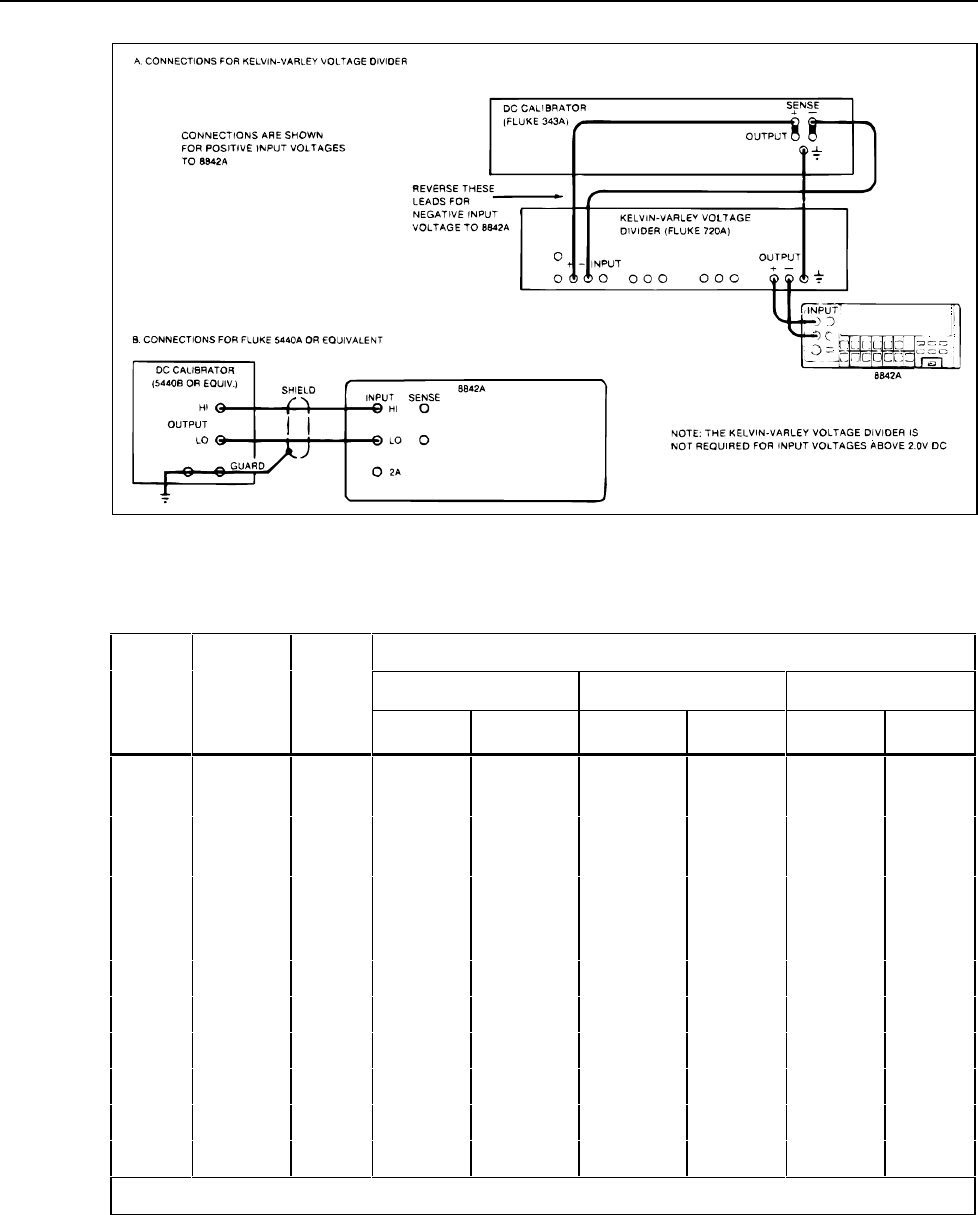
8842A
Instruction Manual
6-6
f6-01.wmf
Figure 6-1. DC Calibration Connections
Table 6-2. DC Voltage Test
Displayed Reading
SLOW MEDIUM FAST
STEP RANGE INPUT
(V dc) MIN MAX MIN MAX MIN MAX
A120 mV 0V
(short)
-0.0030 +0.0030 -0.0050 +0.0050 -0.030 +0.030
B1200 mV 0V
(short)
-00.003 +00.003 -00.005 +00.005 -00.03 +00.03
C12V, 20V,
200V,
1000V
0V
(short)
-2 counts +2 counts -4 counts + 4 counts -3 counts +3
counts
D 20 mV 10 mV +9.9963 +10.0037 +9.9943 +10.0057 +9.970 +10.030
E 200 mV 100 mV +99.993 +100.007 +99.991 +100.009 +99.97 +100.03
F 2V 1V +.99996 +1.00004 +.99994 +1.00006 +.9997 +1.0003
G 20V 10V +9.9995 +10.0005 +9.9993 +10.0007 +9.997 +10.003
H 200V 100V +99.995 +100.005 +99.993 +100.007 +99.97 +100.03
I 1000V 1000V +999.95 +1000.05 +999.93 +1000.07 +999.7 +1000.3
1. Relative to high-quality short stored using OFFSET feature.
Maintenance
PERFORMANCE TEST
6
6-7
6-5. AC Voltage Test (Option -09 Only)
The following procedure may be used to verify the accuracy of the VAC function:
1. Ensure the 8842A is on and warmed up for at least 1 hour.
2. Select the VAC function and the slow (S) reading rate.
3. Connect the AC Calibrator to provide a voltage input to the HI and LO INPUT
terminals.
4. (Low- and Mid-Frequency Test.) For each step in Table 6-3, select the indicated
range, set the AC Calibrator for the specified input, and verify that the displayed
reading is within the limits shown for each reading rate.
NOTE
This procedure tests the extremes of each range. You may shorten the
procedure by testing only the "quick test points" indicated in Table 6-3 with
asterisks.
5. (High-Frequency Test.) For each step in Table 6-4, select the indicated range, set the
AC Calibrator for the specified input, and verify that the displayed reading is within
the limits shown for each reading rate.
NOTE
This procedure tests the extremes of each range. You may shorten the
procedure by testing only the "quick test points" indicated in Table 6-4 with
asterisks.
6. Set the AC calibrator to standby and disconnect it from the 8842A.
Table 6-3. Low- and Mid-Frequency AC Voltage Test
Input Display Readings
Step
Number
Range
Voltage Frequency
Error in
Counts Minimum Maximum
1 2V 0.01000V 200 Hz 181 0.00819 VAC 0.01181 VAC
2 2V 0.10000V 200 Hz 87 .09913 VAC .10087 VAC
3* 2V 0.30000V 200 Hz 101 0.29899 VAC 0.30101 VAC
4 2V 1.00000V 200 Hz 150 0.99850 VAC 1.00150 VAC
5* 2V 1.90000V 200 Hz 213 1.89787 VAC 1.90213 VAC
6 2V 0.10000V 20 Hz 220 0.09780 VAC 0.10220 VAC
7 2V 1.90000V 20 Hz 2380 1.87620 VAC 1.92380 VAC
8 2V .10000V 45 Hz 135 0.09865 VAC 0.10135 VAC
9 2V 1.90000V 45 Hz 765 1.89235 VAC 1.90765 VAC
10* 200 mV 0.001000V 100 Hz 204 00.796 mVAC 190.252 mVAC
11 200 mV 0.190000V 20 kHz 252 189.748 mVAC 190.252 MvAC
* Quick Test points
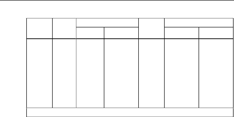
8842A
Instruction Manual
6-8
Table 6-4. High-Frequency AC Voltage Test
INPUT TEST LIMITS (IN VOLTS)
STEP
NUMBER
RANGE
VOLTAGE FREQUENCY
ERROR
IN
COUNTS MIN MAX
1 200 mV 0.010000V 50 kHz 169 09.831 mVAC 10.169 mVAC
2 * 200 mV 0.010000V 100 kHz 350 09.650 mVAC 10.350 mVAC
3 * 2V 0.10000V 100 kHz 350 0.09650 VAC 0.10350 VAC
4 * 20V 1.0000V 100 kHz 350 0.9650 VAC 1.0350 VAC
5 * 200V 10.000V 100 kHz 350 09.650 VAC 10.350 VAC
6 * 700V 100.00V 100 kHz 350 96.50 VAC 103.50 VAC
7 20V 19.0000V 100 kHz 1250 18.8750 VAC 19.1250 VAC
8 200 mV 0.190000V 100 kHz 1250 188.750 mVAC 191.250 mVAC
* Quick test points.
6-6. Resistance Test
The following procedure may be used to verify the accuracy of the 2-wire and 4-wire
ohms functions.
1. Ensure the 8842A is on and has warmed up for at least 1 hour.
2. Connect the Resistance Calibrator to the 8842A for 4-wire ohms.
3. For each step in Table 6-5, select the indicated range, set the Resistance Calibrator
for the specified nominal input. When the input is 0Ω(short), press the OFFSET
switch and verify that the OFFSET anunciator is illuminated.
NOTE
A new OFFSET must be stored for each new range selected.
a. Test the 4-wire ohms function:
1. Select the 4-wire ohms function.
2. Verify that the displayed reading is within the limits shown for
each reading rate.
b. Test the 2-wire ohms function:
1. Select the 2-wire ohms function. (The SENSE test leads need not
be disconnected.)
2. Verify that the displayed reading is within the limits shown for
each reading rate.
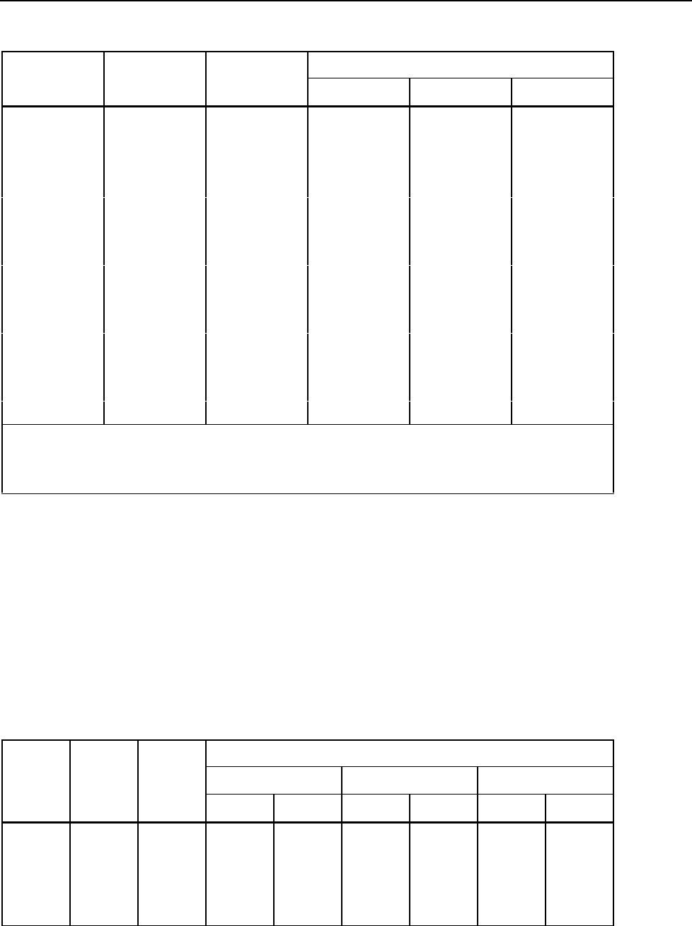
Maintenance
PERFORMANCE TEST
6
6-9
Table 6-5. Resistance Test
Error From Input1 (in counts)Step Range Input
(Nominal) Slow Medium Fast2
120Ω30Ω (short) ±40 ±60 ±20
220Ω310Ω±49 ±69 ±21
3 200Ω30Ω (short) ±4 ±6 ±3
4 200Ω3100Ω±11 ±13 ±4
52 kΩ0Ω (short) ±3 ±5 ±2
62 kΩ1 kΩ±8 ±10 ±3
7 20 kΩ0Ω (short) ±3 ±5 ±2
8 20 kΩ10 kΩ±8 ±10 ±3
9 200 kΩ0Ω (short) ±3 ±5 ±2
10 200 kΩ100 kΩ±9 ±11 ±3
11 2000 kΩ0Ω (short) ±3 ±6 ±2
12 2000 kΩ1 MΩ±28 ±31 ±5
13 20 MΩ0Ω (short) ±4 ±7 ±2
14 20 MΩ10 MΩ±44 ±47 ±6
1 – Using offset control
2 = 4 ½ digit counts
3 = Applies to 4-wire ohms only
6-7. DC Current Test
The following procedure may be used to test the mA DC function:
1. Ensure the 8842A is on and has warmed up for at least 1 hour.
2. Select the mA DC function.
3. Connect the Current Source to the 2A and LO INPUT terminals.
4. For each step in Table 6-6, set the Current Source for the indicated input and verify
that the displayed reading is within the limits shown for each reading rate.
5. Set the Current Source for zero mA and disconnect it from the 8842A.
Table 6-6. DC Current Test
DISPLAYED READING
SLOW MEDIUM FAST
STEP RANGE INPUT
MIN MAX MIN MAX MIN MAX
1 200 mA 0 mA -00.040 +00.040 -00.060 +00.060 -00.20 +00.20
2 200 mA 100 mA 99.920 100.080 99.900 100.100 99.76 100.24
3 2000 mA 0 mA -000.04 +000.04 -000.06 +000.06 -000.2 +000.2
4 2000 mA 1000 mA 999.56 1000.44 999.54 1000.46 999.4 1000.6

8842A
Instruction Manual
6-10
6-8. AC Current Test (Option -09 Only)
The following procedure may be used to test the mA AC function:
1. Ensure the 8842A is on and warmed up for at least 1 hour.
2. Select the mA AC function.
3. Connect the AC Current Source to provide a current input to the 2A and LO INPUT
terminals. If an ac current source is not available, the functionality of the 8842A can
be checked at 10 mA by using a Fluke 5200A set at 100V and connected to the
8842A 2A terminal through a 10 kΩ, 2W, 1% resistor.
4. For each step in Table 6-7, set the AC Current Source for the indicated input and
verify that the displayed reading is within the limits shown for each reading rate.
5. Set the AC Current Source to Standby and disconnect it from the 8842A.
Table 6-7. AC Current Test
INPUT TEST LIMITS
STEP
NUMBER
RANGE
CURRENT FREQUENCY MINIMUM MAXIMUM
1 2000 mA 1900.00 mA 1 kHz 1890.40 1909.60
2 2000 mA 100.00 mA 1 kHz 97.60 102.40
6-9. CALIBRATION
CAUTION
To avoid uncalibrating the 8842A, never cycle power on or off
while the CAL ENABLE switch is on.
NOTE
If U220 is replaced, perform the Erase Cal Memory procedure (located
later in this section) before attempting calibration. Failure to do so may
result in an "ERROR 29" on the 8842A front panel display.
The 8842A features closed-case calibration using known reference sources. The 8842A
automatically prompts you for the required reference sources, measures them, calculates
correction factors, and stores the correction factors in the nonvolatile calibration memory.
Closed-case calibration has many advantages. There are no parts to disassemble, no
mechanical adjustments to make, and if the IEEE-488 Interface is installed, the 8842A
can be calibrated by an automated instrumentation system.
The 8842A should normally be calibrated on a regular cycle, typically every 90 days or 1
year. The frequency of the calibration cycle depends on the accuracy specification you
wish to maintain. The 8842A should also be calibrated if it fails the performance test or
has undergone repair. To meet the specifications in Section 1, the 8842A should be
calibrated with equipment meeting the minimum specifications given in Table 6-1.
The following paragraphs first present a basic calibration procedure. This is followed by
a description of advanced features and special considerations, and by a description of
remote calibration using the IEEE-488 Interface.
Maintenance
CALIBRATION
6
6-11
6-10. Basic Calibration Procedure
The basic calibration procedure consists of the following four parts. These parts must be
performed in the order shown.
1. Initial Procedure.
2. A/D Calibration.
3. Offset and Gain Calibration for each function and range.
4. High-Frequency AC Calibration (True RMS AC option only).
Normally, it is recommended that the entire calibration procedure be performed.
However, under some circumstances the earlier parts may be omitted. For example, if
installing the True RMS AC option, it may be necessary only to perform Offset and Gain
Calibration for the ac functions, followed by High-Frequency AC Calibration. But if the
A/D Calibration is performed, it must be followed by a complete Offset and Gain
Calibration for all functions and then by High-Frequency AC Calibration.
Some of the calibration calculations are complex and take the 8842A some time to
execute. For example, when you store the zero input during the Offset and Gain
Calibration for the VDC function, it takes around 22 seconds before the next prompt
appears. (The 8842A automatically uses this input to calibrate the offset for all ranges.)
While the 8842A is executing a calibration step, it ignores all of the front panel buttons
and postpones execution of all remote commands.
6-11. INITIAL PROCEDURE
Always begin the calibration procedure as follows:
1. Allow the 8842A to stabilize in an environment with ambient temperature of 18°C to
28°C and relative humidity less than 75%.
2. Turn the 8842A on and allow it to warm up for at least 1 hour.
3. Enable the calibration mode by pressing the CAL ENABLE switch with a small
screw-driver or other suitable instrument. (The CAL ENABLE switch is located on
the right side of the display and is normally covered by a calibration seal.)
When the calibration mode is enabled, the CAL annunciator lights up, and the 8842A
displays the first prompt for the A/D Calibration procedure (Figure 6-2). To exit the
calibration mode, press the CAL ENABLE switch again.
f6-02.wmf
Figure 6-2. First A/D Calibration Prompt
In the calibration mode, the front panel controls assume the functions described in Figure
6-3. Some of these functions are advanced features and are not required for the basic
calibration procedure. The display blanks briefly when a button is pressed.
8842A
Instruction Manual
6-12
f6-03.wmf
Figure 6-3. Calibration Functions
The following functions are inappropriate during calibration, and are therefore
unavailable:
• Offset
• Autoranging
• External Trigger
• Front Panel Trigger
• Front panel SRQ (Under local control)
• Diagnostic self-tests
6-12. A/D CALIBRATION
The A/D Calibration procedure calibrates the analog-to-digital converter for offset, gain
and linearity. The 8842A automatically selects the A/D calibration procedure when the
CAL ENABLE switch is first pressed. The procedure must be performed in its entirety,
and may not be performed in part. If the A/D calibration is discontinued prior to
completion, the last complete set of A/D calibration constants will be retained unchanged.
To perform A/D Calibration, proceed as follows:
1. Ensure the Initial Procedure has been completed. The 8842A then displays the
prompt for the first reference source, zero volts (i.e., a short).

Maintenance
CALIBRATION
6
6-13
2. Each time the 8842A prompts you for a reference source, apply the requested source
to the HI and LO INPUT terminals, and press the STORE button. When STORE is
pressed, the numeric display field blanks while the 8842A performs the necessary
calculations. (Do not change the reference source while the display is blank.) The
8842A then displays the next prompt. For reference, all prompts are shown in Table
6-8.
NOTE
The 8842A automatically checks that the reference input is near the value
prompted, and displays ERROR 41 if it exceeds a specific tolerance. (See
Advanced Features and Special Considerations, later in this section.)
3. After the last input is stored, the 8842A begins taking readings in the 2V range of the
VDC function. (The CAL annunciator remains on.) Verify the A/D calibration using
the test points in Table 6-9. If you wish to repeat the A/D Calibration procedure,
press the A/D button.
Table 6-8. A/D Calibration Steps
STEP DISPLAYED PROMPT
A .0 V DC (short)
B - .03 V DC
C - 1.01 V DC
D + .99 V DC
E + .51 V DC
F - .51 V DC
G - .26 V DC
H + .26 V DC
I + .135 V DC
J - .135 V DC
K - .0725 V DC
L + .0725 V DC
Table 6-9. A/D Calibration Verification Test
STEP INPUT A L L O W A B L E
ERROR
A 0V (short) ±2 counts
B -0.03V ±2 counts
C +0.03V-0.660V ±2 counts
D -0.660V ±3 counts
E +0.660V ±3 counts
F -1.970V ±4 counts
G +1.970V ±4 counts

8842A
Instruction Manual
6-14
The A/D Calibration procedure is an iterative process. Each pass through the procedure
uses the constants stored previously and improves them. Normally, one pass is adequate.
However, if the calibration memory has been erased or replaced, or the A/D Converter
has undergone repair, the A/D Calibration procedure must be performed twice.
Because the A/D Calibration procedure is iterative, the instrument’s performance can be
slightly enhanced by going through the procedure more than twice. However, this is not
necessary to meet the published specifications.
6-13. OFFSET AND GAIN CALIBRATION
This procedure calibrates the instrument’s offsets and gains by applying a high and low
input for every range of each function. To save time, the 8842A uses each input for as
many ranges as possible.
A function is calibrated by pressing the corresponding function button. Once a function is
selected, the 8842A automatically steps through each range of that function, prompting
you for the necessary reference sources. (The prompts are shown in Table 6-10.) The
8842A does not automatically select another function after one function has been
completely calibrated; therefore, the functions may be calibrated in any order.
To perform Offset and Gain Calibration, proceed as follows:
Table 6-10. Offset and Gain Calibration Steps
DISPLAYED PROMPT
STEP
VDC VAC12 WIRE kΩ
4 WIRE kΩ
mA DC mA AC1
A +00.0 mV DC (short) 10.0 mV AC 0.00Ω (short) 00.0 mA DC (open) 100 mA AC
B +19.0 mV DC -- 10.0Ω (4 wire) 100 mA DC --
C +190.0 mV DC 100.0 mV AC 100.0Ω1000. mA DC 1000.0 mA AC
D +1.900 V DC 1.000 V AC 1.000 kΩ
E +19.00 V DC 10.00 V AC 10.00 kΩ
F +190.0 V DC 100.0 V AC 100.0 kΩ
G +1000. V DC 500. V AC 1000. kΩ
H Step H not applicable for these
functions. 10.00 MΩ
Steps D-H not applicable for these
functions.
1 Inputs should be at 1 kHz +/-10%. Performance may be enhanced for specific frequencies (see text).
1. Ensure the A/D Calibration procedure has been completed.
2. Select the desired function by pressing the corresponding function button. The 8842A
will display the first prompt for that function.
3. Each time the 8842A prompts you for a reference source, apply this source to the
appropriate terminals, and press the STORE button. When STORE is pressed, the
numeric display field blanks while the 8842A performs the necessary calculations.
(Do not change the reference source while the display is blank.) The 8842A then
displays the next prompt. For reference, all prompts are shown in Table 6-10.

Maintenance
CALIBRATION
6
6-15
NOTE
To use reference sources that differ from the prompted values, see Storing
Variable Inputs later in this section.
4. After the last range is calibrated, the 8842A begins taking readings in the highest
range so that you may verify its calibration. (The CAL annunciator remains on.) To
verify the calibration for the other ranges, press the corresponding range button.
(Pressing a function button begins the Offset and Gain Calibration procedure for that
function.)
5. Repeat steps 2, 3, and 4 for the remaining functions. Note that both 2-wire and 4-wire
ohms functions must be calibrated. (The VAC and mA AC functions require
calibration only if the True RMS AC option is installed.)
NOTE
(True RMS AC option only.) The VAC and mA AC functions should
normally be calibrated using reference sources at 1 kHz (+/-10%). For
special applications, performance may be optimized at other frequencies.
See Optimizing AC Calibration at Other Frequencies, later in this section.
6. When all functions have been calibrated, exit the calibration mode by pressing the
CAL ENABLE switch and attach a calibration certification sticker over the CAL
ENABLE switch. (If the True RMS AC option is installed, instead proceed to the
High-Frequency AC Calibration procedure which follows.)
6-14. HIGH-FREQUENCY AC CALIBRATION
The High-Frequency AC Calibration procedure calibrates the response of the VAC
function from 20 kHz to 100 kHz. If the True RMS AC option is not installed, selecting
this procedure results in an error message.
The reference sources used in this procedure should normally be between 90 kHz and 100
kHz. 100 kHz (nominal) is recommended. For special applications, performance may be
optimized at other frequencies. See Optimizing AC Calibration at Other Frequencies,
later in this section.
To perform High-Frequency AC Calibration, proceed as follows:
1. Ensure Offset and Gain Calibration has been completed for the VAC function.
2. Select the High-Frequency AC Calibration procedure by pressing the HF AC button.
The 8842A will display the first prompt (100 mV AC). The "U" in the display
indicates the High-Frequency AC Calibration procedure has been selected.
3. Each time the 8842A prompts you for a reference amplitude, apply this amplitude to
the HI and LO INPUT terminals, and press the STORE button. When STORE is
pressed, the numeric display field blanks while the 8842A performs the necessary
calculations. (Do not change the reference source while the display is blank.) The
8842A then displays the next prompt. For reference, all prompts are shown in Table
6-11.
NOTE
To use reference amplitudes that differ from the prompted values, see
Storing Variable Inputs later in this section.
4. After the last range is calibrated, the 8842A begins taking readings in the highest
range so that you may verify its calibration. To verify the calibration for the other
ranges, push the corresponding range button. The CAL annunciator remains on.
8842A
Instruction Manual
6-16
5. The calibration procedure is now completed. Exit the calibration mode by pressing
the CAL ENABLE switch, and attach a calibration certification sticker over the CAL
ENABLE switch.
6-15. Advanced Features and Special Considerations
Table 6-11. High-Frequency AC Calibration Steps
STEP DISPLAYED PROMPT1,2
A 100.0 mV AC
B 1.000 V AC
C 10.00 V AC
D 100.0 V AC
E 200.0 V AC
1. The display also indicates “U” to show that HF AC cal is selected.
2. Inputs should be between 90 kHz and 100 kHz. (nominal) is recommended.
The 8842A has several advanced calibration features which are not necessary for the
basic calibration procedure, but which can make calibration easier. The following
paragraphs describe these features and also discuss special considerations for optimizing
the performance of the 8842A in special situations.
6-16. STORING VARIABLE INPUTS
As a convenience, the VAR IN (variable input) feature lets you calibrate the 8842A using
reference source values which differ from the values prompted by the 8842A. For
example, you may want to calibrate the 200Ω range using a reference resistor with a
precisely known value of 99.875Ω, rather than 100Ω as prompted. This feature is not
available during A/D Calibration.
To use the variable input feature, proceed as follows:
1. When the 8842A prompts you for an input, press the VAR IN button. The blank
digits will be replaced with zeroes. You can then increment each digit of the display
by pressing the range buttons. The 20Ω/mV button toggles the displayed sign.
2. Change the displayed prompt to correspond to the desired reference source by
pressing the appropriate range buttons.
3. Connect the desired reference source to the appropriate input terminals of the 8842A.
4. Press the STORE button.
To meet the specifications over all ranges, the reference source for the high prompts must
be between half and full scale. (The high prompts are those prompts that are between
50% and 100% of full scale.) The reference source for the low prompts must be equal to
or greater than the prompted value, but not more than that value plus 4000 counts. (The
low prompts are those prompts that are zero or 5% of full scale.)
For special applications, the 8842A can be calibrated at values outside the recommended
range. This can enhance the performance at the calibration value. However, performance
at other values may be degraded.
Maintenance
CALIBRATION
6
6-17
6-17. CALIBRATING INDIVIDUAL RANGES
During Offset and Gain and High-Frequency AC Calibration, it is possible to calibrate
individually selected ranges. This feature does not apply to the mA DC and mA AC
functions and is not permitted during A/D Calibration.
To calibrate an individual range, proceed as follows:
1. Select the desired calibration procedure by pressing the appropriate function button
(or press the HF AC button if High-Frequency AC Calibration is desired).
2. Press the range button for the range to be calibrated. The 8842A then prompts for a
low reference source for that range. (See Table 6-12.) (During High-Frequency AC
Calibration, the 8842A prompts only for a high reference source. In this case,
proceed to step 4.)
3. Apply the requested reference source and press STORE. The display will blank
briefly and then prompt for a high reference source. (See Table 6-12.)
4. Apply the requested reference source and press STORE. The display will blank
briefly, and the 8842A will then begin taking readings in the selected range so that
you may verify the calibration. The CAL annunciator remains on.
5. To continue, select another range. You may restart any of the calibration procedures
by pressing the appropriate function button, the A/D button, or the HF AC button.
6-18. VERIFYING CALIBRATION
Table 6-12. Prompts When Calibrating Individual Ranges
PROCEDURE FUNCTION LOW PROMPT HIGH PROMPT
VDC Zero 95% of full scale 1
kΩZero 50% of full scale
Offset and Gain
Calibration
VAC 5% of full scale 250% of full scale 2
High-Frequency AC
Calibration (Not applicable) (No low prompt) 50% of full scale 3
1. Exception: The 1000V dc range has a high prompt of 1000V dc.
2. Exception: The 700V ac range has a low prompt of 100V ac and a high prompt of 500V ac.
3. Exception: The 700V ac range has a prompt of 200V ac.
When you complete certain parts of the calibration procedure, the 8842A automatically
begins taking readings so that you can verify the calibration is correct. (It is
recommended that you do so.) The CAL annunciator remains lit. The 8842A continues to
take readings until you select another calibration procedure or exit the calibration mode.
Specifically, the 8842A begins taking verification readings after:
1. Completing A/D Calibration.
2. Completing Offset and Gain or High-Frequency AC Calibration.
3. Completing the calibration of an individually selected range.
While the 8842A is taking verification readings, certain buttons are active or function
differently:

8842A
Instruction Manual
6-18
1. If you just completed the Offset and Gain or High-Frequency AC Calibration for an
entire function (not just one range), the range buttons can be used to change ranges in
order to verify all ranges were calibrated correctly.
2. If you just calibrated an individually selected range, pressing another range button
begins the Offset and Gain Calibration procedure for the new range.
3. You can use the RATE button to verify the calibration at other reading rates.
CAUTION
It is still possible to erase the calibration memory while the
8842A is taking verification readings.
6-19. ERASING CALIBRATION MEMORY
The 8842A allows you to erase some or all of the correction constants stored in
calibration memory (U220). It is recommended that you erase the entire calibration
memory before beginning calibration if the calibration memory is replaced or
accidentally altered. The capability of erasing particular parts of the memory is mainly
intended as a troubleshooting aid to the technician.
CAUTION
Once the calibration memory is erased, the 8842A must be
recalibrated.
To erase all or part of the calibration memory, proceed as follows:
1. Press the front panel ERASE button. The display should show the erase prompt "cl"
(for "clear"). If you do not press another button within 1-1/2 seconds, the 8842A
returns to its previous state.
2. To complete an erasure, press one of the following buttons within 1-1/2 seconds of
pressing the ERASE button:
a. STORE -- Erases the entire memory.
b. A/D -- Erases the A/D Calibration constants
c. Any function button -- Erases the Offset and Gain Calibration constants for all
ranges of that function.
d. HF AC -- Erases the High-Frequency AC Calibration constants.
3. After an erasure is finished (a complete erasure takes about 3 seconds), the 8842A
returns to one of the following states:
a. After complete erasure: Begins A/D Calibration.
b. After A/D erasure: Begins A/D Calibration.
c. After Offset and Gain erasure: Begins Offset and Gain Calibration for erased
function.
d. After High-Frequency AC erasure: Begins High-Frequency AC Calibration.
6-20. TOLERANCE CHECK
The 8842A automatically checks that the reference input is near the value prompted. This
minimizes common errors such as applying a reference source with the wrong sign. If the
reference input exceeds the tolerances shown in Table 6-13, the 8842A displays ERROR
41.

Maintenance
CALIBRATION
6
6-19
If ERROR 41 occurs, the most likely cause is that the reference input is incorrect (e.g.,
has the wrong polarity). If the input is in fact correct, refer to the Troubleshooting
heading in this section.
Table 6-13. Tolerance Limits
CALIBRATION TOLERANCE
1. A/D Calibration ±244 counts from prompt
2. Offset and Gain Calibration
VDC, mA DC ±488 counts from prompt
Ohms ±3002 counts from prompt
VAC, mA AC ±3002 counts from prompt
3. HF AC Calibration ±9999 counts from prompt
6-21. AC CALIBRATION AT OTHER FREQUENCIES
For special applications where the 8842A is to be used to measure ac voltages or currents
exclusively at a single frequency or narrow range of frequencies, accuracy may be
enhanced at that frequency (or range of frequencies) by performing calibration according
to the following procedure. Note that this may degrade the accuracy at frequencies
significantly removed from the frequency of optimization.
To optimize performance at a frequency less than 1 kHz, perform the offset and gain
calibration procedure, above, using the frequency at which measurements will be made
rather than 1 kHz. This technique may be used for both the VAC and mA AC functions.
At the calibration frequency, the 8842A will yield accuracy closely approaching the
specified mid-band performance.
To optimize performance at a frequency greater than 1 kHz, perform calibration as
follows:
1. Perform the Offset and Gain Calibration procedure using inputs at 1 kHz.
2. Perform the High-Frequency AC Calibration procedure using inputs at the desired
frequency of optimization rather than at 100 kHz. Skip step 5 in that procedure
3. Again perform the Offset and Gain Calibration procedure, this time using inputs at
the desired frequency of optimization rather than at 1 kHz.
6-22. OPTIMIZING USE OF THE 5450A
If the Fluke 5450A Resistance Calibrator is used to calibrate the 2-wire ohms function,
the following procedure is recommended to optimize the calibration of the lowest two
ranges. (The 5450A has a 25 mΩ "floor" which would otherwise result in 25 digits of
error in the 200Ω range of the 8842A.) In this procedure, the 8842A is referred to as the
unit under test (UUT).
1. Complete Offset and Gain Calibration for the UUT’s 4-wire ohms function. The
UUT will then be taking verification readings.
2. Connect the UUT to the 5450A as shown in Figure 6-4.
3. Select the "SHORT" from the 5450A, and measure this value at the 5450A OUTPUT
terminals using the UUT in 4-wire ohms. If in remote, take the average of four
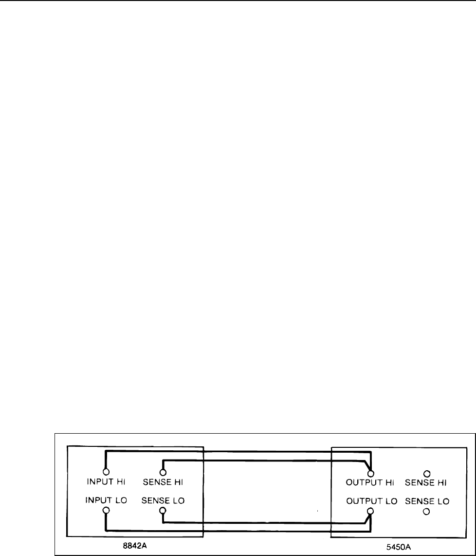
8842A
Instruction Manual
6-20
readings. (In remote calibration, the averaged value can be stored in the controller.)
Record the value.
4. Select the "100Ω" output from the 5450A, and measure this value as in step 3.
5. Find and record the numerical difference between the values calculated in steps 3 and
4. This value will be used as the variable input for calibrating the 200Ω range in 2-
wire ohms.
6. Repeat steps 4 and 5 using the "1 kΩ" output from the 5450A; find and record the
numerical difference between this and the "SHORT" measured in step 3. This value
will be used as the variable input for calibrating the 2 kΩ range in 2-wire ohms.
7. Press the UUT’s 2 WIRE kΩ button. This selects the Offset and Gain calibration
procedure for the 2-wire ohms function and prompts for zero input. Select the
"SHORT" from the 5450A, and calibrate all the zeros by pressing STORE.
8. Select the "100Ω" output from the 5450A and calibrate the high point for the 200Ω
range, entering the value computed in step 5 as a variable input.
9. Select the "1 kΩ" output from the 5450A and calibrate the high point for the 2 kΩ
range, entering the value computed in step 6 as a variable input.
10. Calibrate the remaining ranges (steps D-G of Table 6-10) using the 5450A outputs.
11. Recalibrate the low point for each 2-wire ohms range using a shorting link (Pomona
MDP-S-0 or equivalent) across the UUT’s HI and LO INPUT terminals.
12. Exit the calibration mode by pressing the CAL ENABLE switch.
13. Using the same configuration shown in Figure 6-4, verify that the UUT measures the
same value (within 1 digit) in 2-wire ohms (using the offset feature to correct for
5450A floor error) as in 4-wire ohms. If the readings differ by more than 1 digit,
reenable the calibration mode and repeat steps 2 through 8.
NOTE
Only 4-wire ohm calibration is allowed in the 20
Ω
range.
14. Cover the CAL ENABLE switch with a calibration certification sticker.
f6-04.wmf
Figure 6-4. Optimizing Use of the 5450A
6-23. Remote Calibration
If the IEEE-488 Interface is installed, the 8842A can be calibrated under remote control.
Remote calibration is very similar to local (front-panel controlled) calibration. Table 6-14
shows the remote commands which correspond to the front panel features.To facilitate
remote calibration, there are some differences from local calibration:
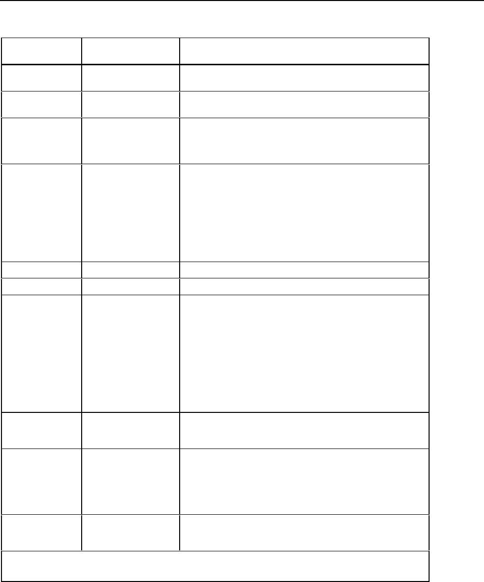
Maintenance
CALIBRATION
6
6-21
Table 6-14. Commands Used During remote Calibration
FRONT PANEL
FEATURE CORRESPONDING
COMMAND COMMENTS
Display G2 Loads the calibration prompt into the output buffer. Not valid
when the 8842A is taking verification readings.
Function Buttons F1 through F6 In the calibration mode, these select the Offset and Gain
Calibration procedure for the corresponding funtion.
Range R1 through R6 and R8 In the calibration mode, these select the Offset and Gain
Calibration Procedure for the corresponding range in the
presently selected function. (For entering variable inputs, see
VAR IN below.)
STORE C0 Tells the 8842A that the requested calibration input is valid.
This command causes the 8842A to take readings, and
compute and store calibration constants.
NOTE
The C0 command can take up to 22 seconds to execute.
You must determine when this command is complete
before sending more commands. See Timing
Considerations in text.
A/D C1 Selects the A/D Calibration procedure.
HF AC C2 Selects the High-Frequency AC Calibration procedure.
ERASE C3 After receiving this command the display shows the erase
mode prompt (‘cl’). (The prompt is not loaded into the output
buffer.) To complete the erasure you must then send C0.
Sending any other command after the C3 command causes
the 8842A to return to its previous state. There is no timeout
as with the front panel ERASE button.
CAUTION
The command string “C3 C0” erases the entire
calibration memory. A complete calibration must then
be performed.
RATE S0 through S2 Changes the reading rate while the 8842A is taking
verification readings. Causes an error at any other time
during calibration.
VAR IN N<value>P2 Enters <value> as a variable input. (See Entering Variable
Inputs, in text.) Causes an error if sent during A/D Calibration
or when the 8842A is taking verification readings. You can
check that the command was successful by checking the
error status or by sending the Get Calibration Input command
(G2).
-- P3<string>Puts the <string> into calibration memory. The string must
contain up to 16 ASCII characters, and be recalled with the
G3 command.
NOTE: Other commands that may be used during calibration are: P1 (Put SRQ mask); the remaining Get
commands; and X0 (clear Error Register).

8842A
Instruction Manual
6-22
1. In remote calibration, you can store a 16-character message in the calibration
memory which can be read by the system controller. Possible uses include
storing the calibration date, instrument ID, etc.
2. Although some buttons are ignored in local calibration (e.g., the AUTO button),
the corresponding remote commands (e.g., R0) load the output buffer with an
error message.
3. The calibration memory is erased differently. (This is explained later.)
4. The rear panel SAMPLE COMPLETE signal acts slightly differently. During
calibration, the SAMPLE COMPLETE signal is inactive. When the 8842A is
taking verification readings, the SAMPLE COMPLETE signal acts the same as
in normal operation.
Note that a command may be valid in some parts of the calibration procedure but not in
others. The Get Input Prompt (G2) command, for instance, is not valid when the 8842A is
taking verification readings. The Rate (Sn) commands, for instance, are valid when the
8842A is taking verification readings, but they are not valid at any other time during
calibration. Table 6-15 shows when commands are invalid.

Maintenance
CALIBRATION
6
6-23
6-24. TIMING CONSIDERATIONS
Table 6-15. Error Numbers Which Are Displayed When Commands Are Not Valid
CALIBRATION MODE
COMMAND NORMAL
MODE
SELFTEST
A/D CAL OFFSET &
GAIN CAL
HF AC CAL VERIFICAT
ION MODE
Bn 60 52 52 52 52
C0 51 60 54
C1 51 60
C2 51 60
C3 51 60
Dn 60 52 52 52 52
Fn 60
G0
G1
G2 51 60 54
G3 60
G4
G5
G6
G7
N
P0 60 52 52 52 52
P1
P2 51 60 56 54
P3 51 60
R0 60 52 52 52 52
R1-6 60 52 52 52 52
R7 60 52 52 52 52
R8 60 52 52
Sn 60 52 52 52
Tn 60 52 52 52 52
Wn
X0
Yn
Z0 60 52 52 52 52
* 6052525252
?60

8842A
Instruction Manual
6-24
The C0 command can take up to 22 seconds. If during this time the controller continues
to send the 8842A more commands, the commands may fill up the 8842A’s input buffer.
If this happens, errors will probably occur.
You can avoid this problem by knowing when these commands are completed. There are
three ways to determine this:
1. Monitoring the Cal Step Complete bit in the serial poll status register. This status bit
is set false every time the remote processor sends a command to the in guard
processor. It is then set true when the in guard processor completes the command and
is ready to accept more. So you can send a command and loop on a check of the
status, until the command is complete.
2. Setting the SRQ mask to generate an SRQ on Cal Step Complete. An SRQ is
generated and the Cal Step Complete bit in the serial poll status response is set when
a cal command is complete. This approach depends on capabilities of the controller
being used.
3. Executing a delay in controller software after sending each command. (Not
recommended.)
Although not usually necessary, these methods can be used for other commands as well.
6-25. REMOTE ERASURE
The C3 command allows you to erase the entire calibration memory. The erasure is
executed by sending the string "C3 C0" (equivalent to pressing ERASE and then
STORE). Any command other than C0 after C3 will abort the erasure. To facilitate
remote calibration, the C0 command does not timeout as does the front panel ERASE
button. The selective erasure that is possible from the front panel is intended as a
troubleshooting aid, and is not available over the IEEE-488 Interface.
Note that the erase command can take up to 3 seconds to execute. To prevent timeout
problems with the controller, you must determine when the command is completed
before continuing. Several methods are presented in Timing Considerations, above.
NOTE
When erasing calibration memory, it is good practice to send the
commands C3 and C0 in the same command string. Sending C3 by itself
could lead to accidentally erasing calibration memory, since the C3
command does not time out as does the ERASE button.
6-26. EXAMPLE CALIBRATION PROGRAM
An example A/D calibration program is shown in Figure 6-5. The program is written in
Fluke BASIC for the Fluke 1722A Instrument Controller. It uses the Fluke 5440A Direct
Voltage Calibrator to perform and then verify the A/D Calibration procedure. In this
program, the 8842A is at bus address 1, and the 5440A is at bus address 7.
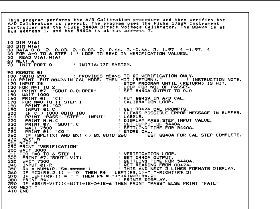
Maintenance
DISASSEMBLY PROCEDURE
6
6-25
f6-05.wmf
Figure 6-5. Example A/D Calibration Program
6-27. DISASSEMBLY PROCEDURE
WARNING
TO AVOID ELECTRIC SHOCK, REMOVE THE POWER CORD
AND TEST LEADS BEFORE DISASSEMBLING THE
INSTRUMENT. OPENING COVERS MAY EXPOSE LIVE PARTS.
CAUTION
To avoid contaminating the printed circuit assemblies (PCAs),
handle the PCAs by their edges. Do not handle the areas of the
PCAs that are not solder masked unless absolutely necessary.
These areas must be cleaned if contaminated.
The following paragraphs present a disassembly procedure for the 8842A. The procedure
should be performed in the order presented. Remove the case first, and then remove
Option -09, the True RMS AC PCA, Option -05, the IEEE-488 Interface PCA, the Main
PCA, and the front panel. For reference, see the final assembly drawing in Section 7.
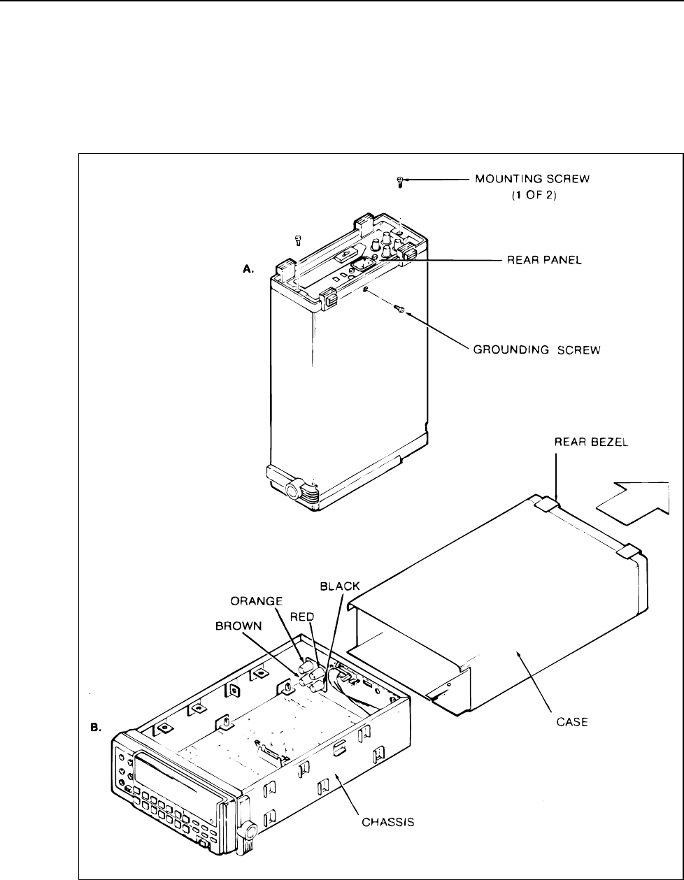
8842A
Instruction Manual
6-26
6-28. Case Removal
1. Remove the grounding screw from the bottom of the case. Remove two rear bezel
mounting screws. (See Figure 6-6A.)
2. While holding the front panel, slide the case and rear bezel off the chassis (See
Figure 6-6B). (At this point, the rear bezel is not secured to the case.)
f6-06_1.wmf
Figure 6-6. 8842A Disassembly
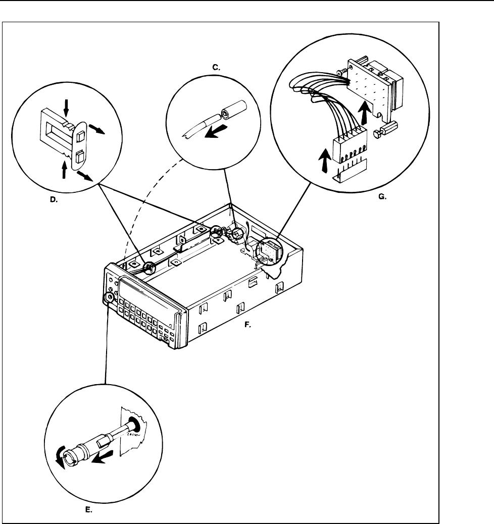
Maintenance
DISASSEMBLY PROCEDURE
6
6-27
f6-06_2.wmf
Figure 6-6. 8842A Disassembly (cont)
8842A
Instruction Manual
6-28
f6-06_3.wmf
Figure 6-6. 8842A Disassembly (cont)
Maintenance
DISASSEMBLY PROCEDURE
6
6-29
f6-06_4.wmf
Figure 6-6. 8842A Disassembly (cont)

8842A
Instruction Manual
6-30
6-29. True RMS AC PCA Removal (Option -09 Only)
The True RMS AC PCA should be removed by reversing the last three steps in Figure
809-1 (see Section 8).
1. Release the True RMS AC PCA from the chassis by pulling the four plastic latches
upward (Figure 809-1E).
2. Raise the True RMS AC PCA slightly, and disconnect the red lead from the
connector (J301) located on the Main PCA (Figure 809-1C).
3. Disconnect the ribbon cable from the Main PCA by releasing the ribbon connector
latches (push outward; see Figure 809-1D) and pulling the ribbon cable directly
outward from the connectors (Figure 809-1C).
4. Lift the True RMS AC PCA out of the chassis.
6-30. IEEE-488 Interface PCA Removal (Option -05 Only)
The IEEE-488 Interface PCA should be removed by reversing the last four steps in
Figure 805-1 (see Section 8):
1. Remove the two jack screws and washers from the rear panel IEEE-488 connector
(Figure 805-1H).
2. Release the IEEE-488 Interface PCA from the chassis by pulling the two plastic
latches upward (Figure 805-1H).
3. Raise the forward edge of the IEEE-488 Interface PCA slightly, pull the PCA
towards the front panel (guiding the IEEE-488 jack and BNC connectors out of the
rear panel), and lift the PCA out of the chassis (Figure 805-1G).
4. Disconnect the ribbon cable from the IEEE-488 Interface PCA by releasing the
connector latches (push outward; see Figure 805-1F) and pulling the ribbon cable out
from the connector (Figure 805-1E).
6-31. Main PCA Removal
1. Disconnect the leads from the four front panel input terminals and the four rear panel
input terminals by unplugging them. (Refer to Figure 6-6C.)
2. Remove the cable harness from the two cable clamps on the side of the instrument
chassis. (Figure 6-6D.) Lift the cable harness clear of the sidewall cable guide.
3. Remove the front panel fuse by pressing in the lip of the 2A input terminal slightly
and rotating it 1/4-turn counterclockwise (Figure 6-6E).
4. (Disregard this step if the IEEE-488 Interface was installed.) Disconnect the ribbon
cable from the rear panel insert by pushing outward on the snap tab on either side of
the ribbon cable connector.
5. Disconnect the two ribbon cables from the Display PCA by pulling the two plastic
pull tabs directly outward from the Display PCA.
6. Remove the two mounting screws on either side of the rear panel power receptacle.
7. Disconnect the green power supply ground lead from the rear panel mounting stud.
(The stud is located near the rear panel power receptacle. See Figure 6-6F.)
8. Remove the Line Voltage Selection Switch (LINE SET) PCA as follows (Figure 6-
6G):
a. Remove the upper screw that holds the LINE SET PCA to the upper rear panel
standoff.

Maintenance
DISASSEMBLY PROCEDURE
6
6-31
b. Unplug the ribbon cable from the Main PCA and lift out the LINE SET PCA.
9. Remove the push rod for the CAL ENABLE switch as follows (Figure 6-6H):
a. While supporting the white plunger of the CAL ENABLE switch with a finger,
pop the push rod off the switch plunger by pulling the push rod directly upward.
b. Rotate the push rod 90 degrees toward the center of the instrument.
c. Pull the push rod toward the rear panel and remove it.
10. Remove the FRONT/REAR switch push rod as follows (Figure 6-6I):
a. Insert a blade-type screw driver in the slot visible on the top of the
FRONT/REAR switch push rod at the junction of the push rod and the switch.
b. Twist the screwdriver slightly to release the push rod from the switch shaft, then
pull the FRONT/REAR switch push rod out through the front panel.
11. Place the chassis on its side.
12. Remove the POWER switch push rod as follows (Figure 6-6J):
a. Insert a blade-type screwdriver in the slot visible on the top of the POWER
switch push rod at the junction of the push rod and the switch.
b. Twist the screwdriver slightly to release the push rod from the switch shaft, then
pull the rear of the POWER switch push rod out through the bottom of the
chassis.
c. Lift the push rod out and toward the rear panel, and remove it.
13. Remove the two screws fastened to the transformer bracket, then remove the bracket.
14. Remove the Main Shield as follows (Figure 6-6K):
a. Remove the screw that fastens the Main Shield to the Main PCA.
b. Grasp the Main Shield supports on one side of the instrument and pull the
supports toward the center of the chassis, bowing the Main Shield. Remove the
main shield.
15. Release the six plastic latches that hold the Main PCA to the chassis by pulling the
latches upward (Figure 6-6L).
16. Lift the front end of the Main PCA upward about 3 inches.
17. Free the white lead from the 2A INPUT tower as follows (Figure 6-6M):
a. Guide the wire, spring and fuse contact toward the front panel.
b. Thread the spring and fuse contact through the hole in the front end of the tower.
18. Slide the Main PCA forwards until it is free of the chassis.

8842A
Instruction Manual
6-32
6-32. Front Panel Disassembly
1. Holding the chassis vertically (with the front panel downward), remove the mounting
screws from the four corners of the Display PCA (Figure 6-7A).
2. Holding the chassis vertically (now standing the instrument on the rear panel), pull
the front panel off the chassis and set it aside (Figure 6-7B).
3. Remove the the display assembly (Display PCA, spacer matrix, and keypad) from the
chassis as follows (see Figure 6-7C):
a. Release the two plastic tabs on the front of the chassis.
b. Let the bottom edge of the display assembly swing toward the rear of the
instrument.
c. Pull the Display PCA toward the bottom of the chassis.
4. Separate the spacer matrix from the Display PCA by releasing the two pairs of plastic
snap tabs on the back of the Display PCA (Figure 6-7D).
5. Remove the keypad from the spacer matrix.
CAUTION
The vacuum fluorescent display should not be removed from
the Display PCA; these are supplied as one part.
6. Remove the display window from the front panel as follows:
a. Slide the window upward (away from the buttons) about 1/32 inch (Figure 6-8A).
b. Push the window directly outward from the front panel (Figure 6-8B).
6-33. REASSEMBLY PROCEDURE
To reassemble the instrument, proceed as follows:
1. Assemble the front panel assembly by reversing the front panel disassembly
procedure (Figure 6-7). (It is easiest to lay the keypad on the Display PCA before
installing the spacer matrix on the Display PCA.)
CAUTION
The four Display PCA mounting screws are self-tapping. To
avoid damaging the threads, ensure the screws are threaded
properly before tightening. Do not overtighten them.
2. Turn the chassis upside down.
3. Install the Main PCA through the bottom of the chassis as follows:

Maintenance
REASSEMBLY PROCEDURE
6
6-33
NOTE
When installing the Main PCA, guide the rear ribbon cable around the
shield connected to the rear panel so that the cable is next to the side of the
chassis. Make certain that the cable is not pinched between the shield and
the Main PCA.
a. Slide the Main PCA toward the rear panel, and position the power connector and
fuse to fit through their respective openings in the rear panel.
b. Reinstall the white lead in the 2A INPUT tower and reinstall the 2A fuse in the
front panel.
c. Make sure the six plastic latch heads are extended. Lower the Main PCA into
position on the chassis and guide the six plastic latches into the circuit board
supports on the chassis. Press the latch heads to lock the board in the chassis.
Refer to Figure 6-6L. 4. Install one side of the Main Shield; bow it to install the
the other side, and secure it to the Main PCA with the retaining screw. 5. Place the
transformer bracket back into position and fasten down with the two screws.
6. Replace the push rod for the POWER switch as follows:
a. Insert the button end of the push rod into the rear of the front panel.
b. While supporting the opposite side of the plunger with your finger, snap the other
end of the push rod onto the POWER switch plunger. Refer to Figure 6-6J.
7. Set the chassis right side up.
8. Insert the FRONT/REAR switch push rod through the front panel and snap it into
place.
9. Reinstall the CAL ENABLE switch push rod by inserting the cylindrical end of the
push rod into the rear of the front panel, then snapping it onto the CAL ENABLE
switch plunger.
8842A
Instruction Manual
6-34
f6-07.wmf
Figure 6-7. Front Panel Disassembly
Maintenance
REASSEMBLY PROCEDURE
6
6-35
f6-08.wmf
Figure 6-8. Removing the Display Window
CAUTION
Make certain that the CAL ENABLE switch shaft is in the out
(disabled) position after the CAL ENABLE push rod is installed.
If the 8842A is switched on with the CAL ENABLE switch in the
enabled position, the 8842A may require recalibration.
10. Position the slot in the lower edge of the Line Voltage Selection Switch PCA in the
slot on the lower rear panel standoff. Secure the top of the Line Voltage Selection
Switch PCA to the upper standoff using the single mounting screw, and plug the
ribbon cable into the Main PCA.
11. Connect the power supply ground lead to the rear panel mounting stud. (The stud is
located near the rear panel power receptacle as shown in Figure 6-6F.)
WARNING
TO AVOID ELECTRIC SHOCK, ENSURE THAT THE POWER
SUPPLY GROUND LEAD IS FIRMLY ATTACHED TO THE
REAR PANEL MOUNTING STUD.
12. Attach the two mounting screws on either side of the rear panel power receptacle.
13. Connect the two ribbon cables to the Display PCA to the connectors. Push the cables
straight in to avoid damage.
14. Reinstall the harness in the sidewall cable guide, and secure the harness to the chassis
with the cable clamps.
15. Connect the leads to the four front panel input terminals according to the color codes
marked on the rear side of the Display PCA.
16. Connect the leads to the four rear panel input terminals following the color codes as
shown in Figure 6-6B.
17. (Option -05 only) Install the IEEE-488 Interface PCA according to the instructions in
Section 8.
18. (Option -09 only) Install the True RMS AC PCA according to the instructions in
Section 8.
19. Slide the case and rear bezel onto the chassis.
20. Install the two rear panel mounting screws.
21. Install the case grounding screw in the bottom of the case.

8842A
Instruction Manual
6-36
WARNING
TO AVOID ELECTRIC SHOCK, ENSURE THAT
THE GROUNDING SCREW IS FIRMLY
ATTACHED TO THE CASE BOTTOM.
6-34. INTERNAL FUSE REPLACEMENT
CAUTION
For fire protection, use exact fuse replacements only.
The 8842A has an internal 3A 600V slow-blow fuse (F301) in series with the 2A input
terminal. To replace this fuse, remove the case according to the disassembly instructions.
The fuse is held in fuse clips on the Main PCA. Do not use makeshift fuses or short-
circuit the fuse holder.
6-35. EXTERNAL TRIGGER POLARITY SELECTION (Option -
05 Only)
The EXT TRIG input is factory-configured with negative polarity (trigger on falling-
edge). This polarity is set by jumper E902 on the IEEE-488 Interface PCA. To select
positive polarity (trigger on rising-edge), remove jumper E902 and add jumper E903.
6-36. TROUBLESHOOTING
The 8842A is designed to be easily maintained and repaired. Both the analog and digital
circuits have built-in diagnostic self-tests and troubleshooting modes to facilitate
troubleshooting and repair. The instrument’s circuits allow troubleshooting and repair
with basic electronic troubleshooting equipment such as a multimeter and oscilloscope.
The troubleshooting mode in the digital controller circuitry generates special test signals
to allow troubleshooting and repair without a special test signal generator or complex
logic analyzer. Using the information in this section, a technician should be able to
troubleshoot and repair the 8842A very efficiently. There is also a troubleshooting
package available which utilizes the Fluke 9010A System Troubleshooter. The 8842A-
9000 Troubleshooting Kit is described in detail in Section 8.
6-37. Initial Troubleshooting Procedure
WARNING
TO AVOID INJURY OR EQUIPMENT DAMAGE, USE EXACT
REPLACEMENT PARTS FOR ALL PROTECTION COMPONENTS.
When a problem occurs in the 8842A, first verify the problem is actually in the
instrument. If the problem occurs when the instrument is in a system, check to see if the
same problem exists when under local control. Watch the display as the instrument is
turned on to see if any of the digital self-test error codes appear indicating a digital
failure. If the malfunction does not involve the True RMS AC or IEEE-488 options,
remove the option(s) from the instrument before proceeding.

Maintenance
TROUBLESHOOTING
6
6-37
If the display lights up, perform the self-test by pressing the SRQ button for 3 seconds.
(Remember, the input terminals must be disconnected from the test leads during the self-
tests. Otherwise, the 8842A may indicate errors are present.) The test numbers will
appear consecutively. "ERROR" will appear on the display if a test should fail. The
8842A can be held in each of the test configurations by momentarily pressing the SRQ
button. (Press any button to continue the tests.) With the description of the self-tests
given below, it may be possible to isolate the failure. For reference, the states of various
switches and logic lines are shown in Table 6-16 for each function, range, and reading
rate.
If only one or a few failures appear in the self-tests, the problem is usually in the DC
Scaling circuit. By carefully analyzing which failure(s) occurred, the fault can be located
to within a few components. (Table 6-17 shows which components are exercised by each
of the analog tests.) The heading DC Scaling Troubleshooting provides detailed
instructions on locating and repairing DC Scaling circuit problems. However, before
troubleshooting the DC Scaling circuit, all of the power supply levels should be measured
to verify they are within the limits specified in Table 6-23 under Power Supply
Troubleshooting, later in this section.
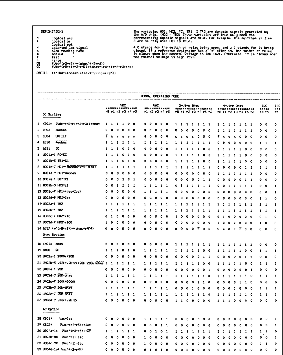
8842A
Instruction Manual
6-38
Table 6-16. Overall State Table
t6-16_1.wmf
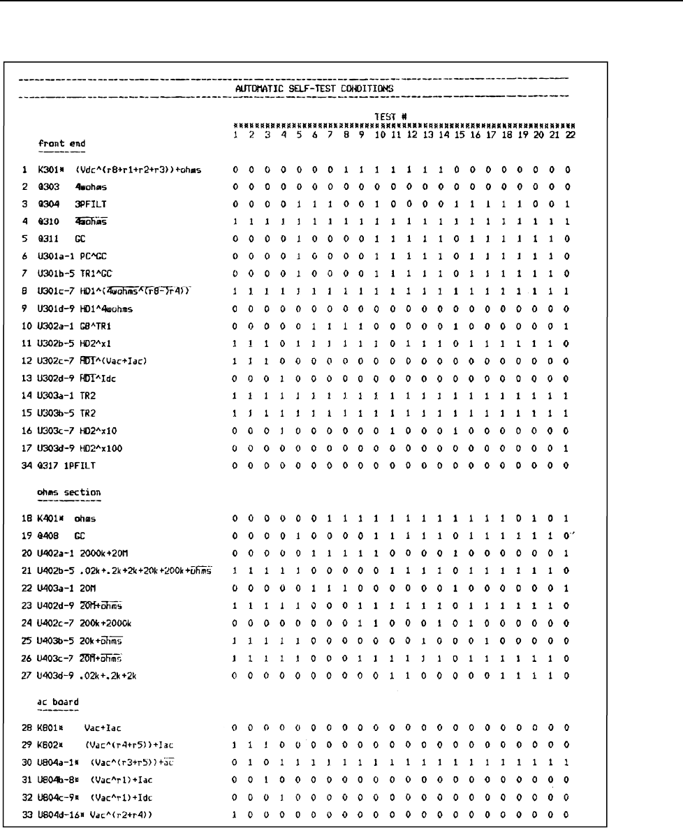
Maintenance
TROUBLESHOOTING
6
6-39
Table 6-16. Overall State Table (cont)
t6-16_2.wmf
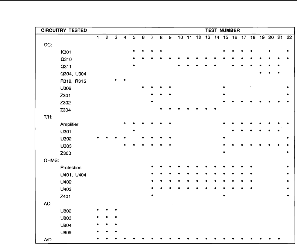
8842A
Instruction Manual
6-40
Table 6-17. Circuitry Tested by the Analog Self-Tests
t6-17.wmf
Some failures will cause many self-tests to fail. If this occurs, the fault is usually in the
Track/Hold circuit, the A/D Converter, the Digital Controller circuit, or the Power
Supply. Again, measure all of the power supply levels according to the limits specified in
Table 6-23. The next step is to isolate the problem to a specific section.
If the self-tests display a large number of errors or if readings are noisy and/or in error,
the problem is usually in the A/D Converter or Track/Hold circuit. (A large number of
errors can also be caused by a problem in the Ohms Current Source.) To isolate the
problem, connect a jumper between TP103 and Reference Low (TP306, or the L-shaped
shield around U202). The display should typically read less than approximately 35 counts
(i.e., +/-.000XX where XX is less than 35) on the 2V dc range. If a good reading can be
obtained (less than approximately 35 counts), the A/D Converter and Precision Voltage
Reference circuits are most likely good. A more conclusive test can be made by
connecting a low-impedance dc source between Reference Low and TP103 with an
output voltage between -2.0V and +2.0V. The reading on the display will be of opposite
polarity to the voltage applied to TP103. (Disconnecting one end of R318 will usually
make it possible to display readings within 0.1% to 0.5% of the actual input.) After it has
been determined that the A/D Converter or the Track/Hold circuit is not functioning
properly, proceed to the corresponding heading for detailed troubleshooting instructions
and guidelines.

Maintenance
TROUBLESHOOTING
6
6-41
A failure in the instrument may cause the 8842A to display random patterns or nothing at
all. Usually, analog circuit failures do not cause the display to go blank or display random
patterns. The best place to start troubleshooting a "dead" instrument or an instrument with
a non-functional display is to check the power supply with a voltmeter for proper levels
and to use an oscilloscope to check the supplies for oscillations. If all of the supplies are
working correctly, check the clock for the In-Guard µC at U202-2. The signal should be
an 8 MHz sine wave approximately 3.5V peak-to-peak. Then check the 1 MHz output of
the A/D IC (U101) at U212-3. (If not present, check at the A/D IC at U101-14.) The
signal should be a 1 MHz square wave approximately 5V peak-to-peak. The 8 MHz sine
wave is generated by the clock circuit of the In-Guard µC, and the 1 MHz signal is the 8
MHz signal divided by a counter in the A/D IC. If the clock signals are correct, proceed
to the heading Digital Controller Troubleshooting, below, for detailed troubleshooting
instructions.
If a problem occurs in the keyboard/display area, the instrument may appear to be totally
inoperative even when the measurement circuitry is still functional. The heading Digital
Controller Troubleshooting provides detailed instructions on locating problems in the
display/keyboard system.
Finally, as in most processor-based systems, there are communication links between the
various parts of the system. Specifically, in the 8842A, there is a bus interface between
analog and digital control circuits and a guard-crossing interface between logic circuits
which may be separated by large potentials. Failures in these links can generate problems
that may be difficult to locate and repair. However, such failures will in turn cause
failures in some analog and or digital section. Thus, indirectly, troubleshooting the
affected section will lead to correction of problems in the internal bus or guard-crossing
circuit.
6-38. Diagnostic Self-Tests
To run the diagnostic self-tests, disconnect the test leads and press the SRQ button for 3
seconds. If the test leads are left attached to the input terminals the 8842A may indicate
errors are present (most likely, errors 5, 7, 8, 9, and 10). Also, if the FRONT/REAR
switch is in the REAR position, the 8842A skips tests 3 and 4, and if Option -09 is not
installed, the 8842A skips tests 1, 2, and 3. For all tests, there is a 0.5 second delay period
before any readings are taken. The tests are all contingent on the A/D Converter being
properly calibrated, but do not depend on the Offset and Gain Calibration constants.
Failing the tests indicates that key portions of the 8842A are not performing properly.
Passing the tests gives approximately a 90% probability that all VDC ranges and range r6
of 2-wire ohms can be calibrated. Passing the tests also gives a reasonable probability
that it will give accurate measurements in VDC and range r6 of 2-wire ohms. However,
passing the tests does not guarantee that the instrument can be calibrated in VAC, mA
DC, mA AC, 4-wire ohms, or ranges r1 to r5 of 2-wire ohms.
NOTE
If the A/D Converter or Precision Voltage Reference is not working, all
analog tests would show an error. If the A/D Converter is not calibrated,
tests 7, 15, 19 could show an error.
If the analog self-tests indicate an error, it may be possible to isolate the problem as
follows:
1. While the error code is being displayed, press the SRQ button. This latches the
8842A into the particular test configuration.
2. Referring to Table 6-18, check that the test point voltages are as shown using another
DMM.

8842A
Instruction Manual
6-42
6-39. Self-Test Descriptions
Table 6-18. Self-Test Voltages
TEST NUMBER TEST POINT VOLTAGE
1 TP803 ±5 mV dc
2 TP803 ±5 mV dc
3 TP803 ±5 mV dc
4 TP103 T/H output waveform for zero input (Figure 6-14)
5 TP302 ±5 mV dc
6 TP302 ±5 mV dc
7 TP302 +50 mV dc typical
8 TP302 +11.5V dc typical
9 TP302 +11.5V dc typical
10 TP302 +4.5V dc with possibly 1V ac (p-p) at 10 Hz
11 TP302 +4.5V dc with possibly 1V ac (p-p) at 10 Hz
12 TP302 +4.5V dc with possibly 1V ac (p-p) at 10 Hz
13 TP302 +4.5V dc with possibly 1V ac (p-p) at 10 Hz
14 TP302 +4.5V dc with possibly 1V ac (p-p) at 10 Hz
15,22 TP302 +50 mV dc typical
16 TP302 +49 mV dc typical
17 TP302 +53 mV dc typical
18 TP302 +59 mV dc typical
19 TP302 <±5 mV dc
20 TP302 +59 mV dc
21 TP302 <±5 mV dc
Note: To measure these correctly, each test must be stopped using the SRQ button.
Also use TP306 (or L-shaped shield around U202) as Reference low.
• TEST 1: 200 VAC, Zero
Configures the 8842A in the 200V ac range (except that K801 is opened) and measures
the open-circuit floor reading. In this range, the first and second stage buffers effectively
divide any noise at the input terminals by 100. This test should be fairly immune from
noise because the input terminals are always open-circuited except for capacitive
feedthrough across K801.
• TEST 2: 700 VAC, Zero
Configures the 8842A in the 700V ac range and measures the open-circuit floor reading.
In this range, the open-circuit reading is divided by 1000. Again, K801 is opened to
reduce sensitivity to external noise.
• TEST 3: mA AC, Zero
Configures the 8842A exactly as in the mA AC function and takes a reading of the
voltage across the 0.1Ω current shunt at the slow reading rate.
• TEST 4: mA DC, Zero

Maintenance
TROUBLESHOOTING
6
6-43
Configures the 8842A in the mA DC function and the slow reading rate, and measures
the reading across the 0.1Ω current shunt. This test should be fairly immune to outside
noise because the total driving impedance is typically less than 1 kΩ. The reading is not a
perfect zero because of the offsets generated by charge injection of U302 and the T/H
Amplifier (X10 configuration).
• TEST 5: 200 VDC, Zero
Configures the 8842A in the 200V dc range and slow reading rate. Input noise is divided
by 100. Assuming no input of any kind, the T/H Amplifier is essentially shorted to
ground by 100 kΩ and filtered by the 3-pole analog filter. Any non-zero reading under
quiet input conditions is due to the offset of the T/H Amplifier (X1 configuration).
• TEST 6: 1000 VDC, Zero
Configures the 8842A exactly as in the 1000V dc range and slow reading rate, with input
noise being divided by 1000. The reading is very close to zero because of the inherent 2
kΩ driving impedance to the T/H Amplifier (X1 configuration).
• TEST 7: 1000 VDC + 20 MΩ
Couples the 1000V dc range and 20 MΩ current source together. The result is nominally
500 nA through the 10 MΩ input divider. Since the 1000V dc range senses this voltage at
the divide-by-1000 point of the scaling circuit, the reading should be 5 mV, or 500 counts
at the A/D Converter. This test could indicate an error if input capacitance is greater than
1000 pF.
• TEST 8: 20 VDC + 20 MΩ
Puts the DC Scaling circuit into the 20V dc range and the Ohms Current Source into the
20 MΩ range. The infinite input impedance of the 20V dc range causes the 20 MΩ
current source to be clamped at its maximum open circuit voltage, typically 12V. The
20V dc range scales this voltage and presents the A/D Converter with 1.15V, or 115,000
counts.This is a good test to ensure that the maximum open-circuit voltage of the Ohms
Current Source is less than 13V. This test is susceptible to capacitance greater than 0.01
µF at the input terminals.
• TEST 9: 20 VDC + 2000 kΩ
Puts the DC Scaling circuit in the 20V dc range and the Ohms Current Source in the 2000
kΩ range. The infinite input impedance of the 20V dc range causes the 2000 kΩ current
source to be clamped at typically 11.5V. The reading at the A/D Converter should be
1.15V. Again tests that the maximum open-circuit voltage of the Ohms Current Source is
less than 13V. Capacitances greater than 0.1 µF at the input terminals can cause an error.
• TEST 10: 2 VDC + 2000 kΩ
Puts the DC Scaling circuit in the 2V dc range and the Ohms Current Source in the 2000
kΩ range, except that its maximum open-circuit voltage is limited to less than 6.5V in
this configuration. This test, as well as tests 11-13, checks clamps Q312 and Q313 and
the analog filter. The reading at the A/D Converter should be an overload. Capacitances
greater than 0.5 µF at the input terminals can cause an error.
• TEST 11: 200Ω, Overrange
• TEST 12: 2 kΩ, Overrange
• TEST 13: 20 kΩ, Overrange
• TEST 14: 200 kΩ, Overrange

8842A
Instruction Manual
6-44
These tests put the 8842A in the respective range of the 2-wire ohms function. They
check that each range of the Ohms Current Source has enough compliance voltage to
overload the dc front end.
• TEST 15: 1000 VDC + X10 T/H + 20 MΩ
Puts the Ohms Current Source in the 500 nA range. The resulting current through Z302
(the 10 MΩ input divider) causes a nominal divider output voltage of 50 mV. The T/H
Amplifier is in X10; thus the A/D Converter sees 50 mV, or 5000 counts. This test can be
susceptible to input capacitances above 1000 pF.
• TEST 16: 200 VDC + 200 kΩ
• TEST 17: 200 VDC + 20 kΩ
• TEST 18: 200 VDC + 2 kΩ
These three tests put the DC Scaling circuit in the 200V dc range and the Ohms Current
Source in the respective current range. The 10M ohm input divider (Z302) senses the
maximum open-circuit voltage of each range of the current source, and the T/H Amplifier
(X1) presents the compliance voltage divided by 100 to the A/D Converter. Nominal
readings should be 49 mV for Test 16, 53 mV for Test 17, and 59 mV for Test 18. All
three tests have a pass limit of 65 mV, insuring that no more than 6.5 volts appears at the
input terminals.
• TEST 19: 200 VDC, Filter On
Test 18 (above) ties the 1 mA range of the Ohms Current Source into the 200V dc range,
with the three-pole analog filter on, such that the A/D reads 59 mV nominal. Test 19
decouples the DC Scaling circuit from the Ohms Current Source; the In-Guard µC waits
28 ms and determines if the voltage at Z302-3 (the divide-by-100 point of the 10 MΩ
input divider) has not discharged to zero volts, due to the long time constant of the filter.
• TEST 20: 200 VDC + 2 kΩ, Filter Off
• TEST 21: 200 VDC, Filter Off
• TEST 22: x100 T/H
The T/H Amplifier is configured in x100 mode. DC stimulus of 5 mV (similar to test 15)
is amplified to 500 mV, which is applied to the A/D converter. This test can be
susceptible to input capacitance above 1000 pF.
Test 20 ties the 1 mA range of the Ohms Current Source into the 200V dc range, with the
3-pole analog filter off, such that the A/D Converter reads 59 mV nominal. Test 21 then
decouples the DC Scaling circuit from the ohms current source; the In-Guard µC waits 28
ms and determines if the voltage at Z302-3 is at zero volts.
• TEST 25: In-Guard µC Internal RAM (U202)
A GALPAT test is performed on the internal RAM of the In-Guard µC. If there are any
errors, ERROR 25 is displayed. This test is performed only upon powerup.
• TEST 26: Display RAM (U212)
A pattern is written to the Display RAM and read back for comparison.If there are any
differences ERROR 26 is displayed.
• TEST 27: In-Guard µC Program Memory (U202)
A two-byte check sum is calculated over the entire 4K Internal Program Memory and
compared with the checksum bytes at the end of that memory. A special add and shift
algorithm minimizes the possibility of double errors cancelling. If something is wrong
with the Internal Program Memory, ERROR 27 is displayed.

Maintenance
TROUBLESHOOTING
6
6-45
• TEST 28: External Program Memory (U222)
A two-byte check sum is calculated over the entire 4K External Program Memory and
compared with the checksum bytes at the end of that memory. A special add and shift
algorithm minimizes the possibility of double errors cancelling. If something is wrong
with the External Program Memory, ERROR 28 is displayed.
• TEST 29: Calibration Memory (U220)
Numerous single-byte checksums are placed in the Calibration Memory, one at the end of
each group of calibration constants. They are calculated in such a way that the single-byte
sum of all bytes in the Calibration Memory add to zero (all carries discarded) and the
single-byte sums of each group also add to zero. A new checksum is calculated and
written to Calibration Memory each time a full or partial calibration is performed. If the
Calibration Memory is not properly configured or not working correctly, ERROR 29 is
displayed. The accuracy of the 8842A is suspect.
6-40. Digital Controller Troubleshooting
The basic strategy in troubleshooting the Digital Controller circuit is to check first
whether the In-Guard Microcomputer (µC) system is functional, starting with the In-
Guard µC itself (U202). Most of this circuitry is tested using the specially provided In-
Guard Troubleshooting Mode.
If the In-Guard µC system proves to be functional, then basic instrument control is
assured and troubleshooting efforts can proceed in one of two directions. If the display
and keyboard appear to be malfunctioning, then they should be checked next. (See
Display System, below.) If the display and keyboard are functioning correctly, you can
omit Display System troubleshooting and proceed to verify that signals are arriving
correctly at the inputs of the analog control devices. (See Analog Control Signals, below.)
If these are also correct, the digital controller is functioning correctly, and you can
proceed to the appropriate analog troubleshooting procedure.
NOTE
For the convenience of the following tests, Options -05 and -09 should be
removed if present. They should only be removed in the power-off
condition.
6-41. IN-GUARD MICROCOMPUTER SYSTEM
This procedure is performed entirely in the In-Guard Troubleshooting Mode. This mode
is established by shorting TP205 (U202-38) to Reference Low (TP306, or the L-shaped
shield around U202) prior to turning on the instrument. Refer to Figure 6-9. To maintain
this mode, the short must remain in effect after the instrument is turned on. When this is
done, the µC programs U202-38 as an input (it is normally an output) to preclude any
possibility of damage due to the short.
CAUTION
To avoid damaging the µC, the short must be initiated before
the instrument is turned on, not after.
The In-Guard Troubleshooting Mode also programs all the normal port outputs to display
a 1 kHz square wave except that the IEEE-488 output (U202-4) sends the word "55"
repeatedly at a rate of 2,000 words/second and the A/D trigger (U202-40) is a square
wave at its normal frequency of 80 Hz, and DM and P23 stay high. (The data received at
U202-5 is meaningless.) Adjacent port outputs display opposite phases of the 1 kHz
square wave. All µC pins that are normally only programmed as inputs are also
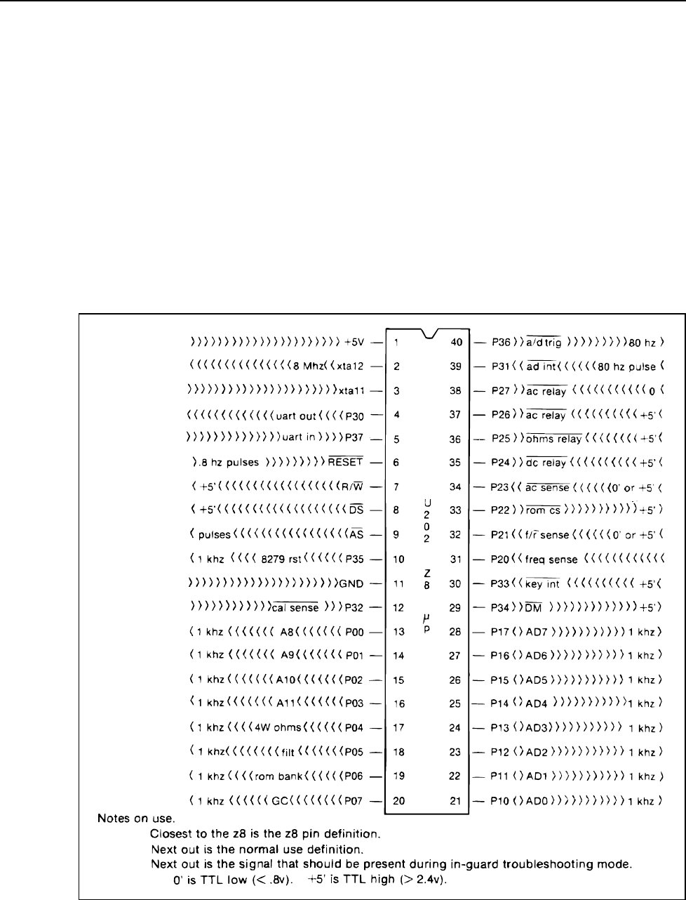
8842A
Instruction Manual
6-46
programmed as inputs to prevent contentions between them and the outputs from other
ICs which drive them. Data coming into all µC inputs (except pin 38) is ignored.
NOTE
If the A/D IC (U101) is working properly, its watchdog timer briefly
interrupts all of the In-Guard Troubleshooting Mode signals every 1.5 sec
for a period of about 0.2 sec. (The signals are then re-established.) If this
occurs, the main counter in U101 and its watchdog timer are operating
correctly. (See step 6, below.)
When the test is complete, turn off the 8842A and remove the short from TP205.
6-42. In-Guard Microcomputer
While the 8842A is in the In-Guard Troubleshooting Mode, check the following in the
order shown:
f6-09.wmf
Figure 6-9. U202 Pin Diagram
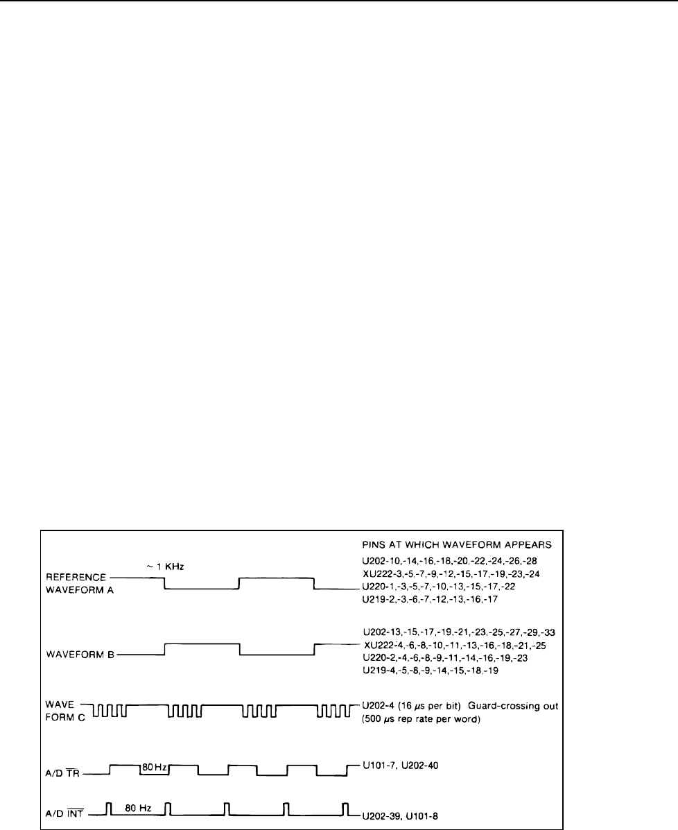
Maintenance
TROUBLESHOOTING
6
6-47
1. Power supplies: +5V dc at U202-1; 0V dc U202-11.
2. µC clock output: 8 MHz at U202-2,-3.
3. Trigger line U202-40 (TP201): Square wave, 50% duty, low 0V, high 3.8V
(nominal). The period of the trigger signal should be 12.500 ms for 60 Hz line.
4. Interrupt from A/D (U202-39): Normally low, duration 48 µs occurs approximately
5450 µs after falling edge of trigger signal on TP201 (U202-40).
5. Guard-crossing test pattern (U202-4): Waveform C (see Figure 6-10).
6. Interrupts from watchdog timer (U202-6): Pulsed low for 0.2 sec every 1.5 sec,
exponential rise between pulses.
7. Output test patterns (see Waveforms A and B in Figure 6-10): 1 kHz square wave on
indicated pins, 50% duty cycle, low 0V, high 3.8V nominal. (The waveforms are
interrupted every 1.5 sec for 0.2 sec due to interrupts from the watchdog timer.) To
observe these patterns, remove U220, attach a logic clip to address latch U219 and
sync on U219-3 for Reference Waveform A on channel 1 of a dual trace scope.
Compare channel 1 with waveforms at U202-10,-14,-16,-18,-20,-22,-24,-26,-28.
These should all be the same as reference Waveform A (including phase). Then
compare channel 1 with waveforms at U202-13,-15,-17,-19,-21,-23,-25,-27,-29,-
33.These should be the same as Waveform B, which is simply the opposite phase of
Waveform A.
6-43. Address Latch (U219)
Verify that U219-2, -6, -7, -12, -13, -16, -17 are the same as Waveform A (see Figure 6-
10) on U219-3. Verify that U219-4, -5, -8, -9, -14, -15, -18, -19 are the same as
Waveform B. The waveforms should be interrupted every 1.5 sec for 0.2 sec due to
interrupts from the watchdog timer.
f6-10.wmf
Figure 6-10. Waveforms for In-Guard Troubleshooting Mode
6-44. External Program Memory (XU222)
Sync on U219-3. Verify that XU222-3, -5, -9, -12, -15, -17, -19, -23, -24 are the same as
Waveform A (see Figure 6-10) on U219-3. Verify that XU222-4, -6, -8, -10, -11, -13, -

8842A
Instruction Manual
6-48
16, -18, -21, -25 are the same as Waveform B. The waveforms should be interrupted
every 1.5 sec for 0.2 sec due to interrupts from the watchdog timer. (Note: XU222 pins
refer to a 28-pin socket.)
6-45. Calibration Memory (U220)
Sync on U219-3. Verify that U220-1, -3, -5, -7, -10, -13, -15, -17, -22 are the same as
Waveform A (U219-3). Verify that U220-2, -4, -6, -8, -9, -11, -14, -16, -19, -23 are the
same as Waveform B. The waveforms should be interrupted every 1.5 sec for 0.2 sec due
to interrupts from the watchdog timer.
6-46. Relay Buffer (U201)
At this point it is necessary to return the 8842A to the normal operating mode by turning
the power switch off, removing the short from TP205 (U202-38), and installing the True
RMS AC option, if present, so that U201-14, -15 may be checked. Power up the
instrument. Unlike the previous checks, outputs are steady state and therefore do not
require a sync signal. Logic "1" is approximately 4.3V dc.
Check that U201-14 is high (4.3V) for mA AC and all ranges of VAC, and low for all
other functions.
Check that U201-15 is high (4.3V) for mA AC and 200V ac and 700V ac ranges, and low
for all other functions.
Check that U201-16 is high (4.3V) for all 2-wire and 4-wire ohms ranges, and low for all
other functions.
Check that U201-17 is high (4.3V) for the lowest three VDC ranges and all 2-wire and 4-
wire ohms ranges, and low for all other functions.
6-47. 3-to-8 Chip Select Decoder (U208)
Make the following checks in the normal operating mode using the fast reading rate and
any function and range. These sequences begin 5.5 ms after the A/D trigger, which is the
falling edge at U202-40.
Check U208-13 for 0.2 µs pulses, normally high, groups of 1, pulse spacing: 10 ms.
Check U208-12 for 0.2 µs pulses, normally high, groups of 1, pulse spacing: 10 ms (10
µs after pin 13).
Check U208-11 for 0.2 µs pulses, normally high, groups of 1, pulse spacing: 10 ms (46
us after pin 13).
Check U208-15 for 0.2 µs pulses, normally high, groups of 13, group width: 100 µs,
group spacing: 10 ms (230 µs after pin 13).
Check U208-7 for 0.6 µs pulses, normally high, groups of 5, group width: 50 µs, group
spacing: 10 ms (380 µs after pin 13).
This concludes testing of the basic µC system. If the keyboard or display is still suspect at
this point, proceed to Display System, below. Otherwise proceed to Analog Control
Signals, below.
6-48. DISPLAY SYSTEM
The display/keyboard system is operated by a complex LSI IC (U212). Generally, this IC
is checked indirectly by observing behavior of the simpler logic devices which it drives.
If the keyboard is working at all, the 8842A display should be "frozen" to make the
following tests. This places the 8842A in a special display test configuration. If it is not
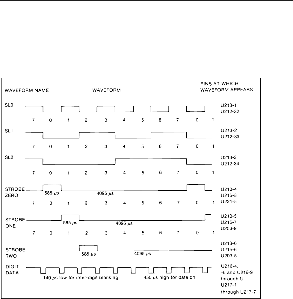
Maintenance
TROUBLESHOOTING
6
6-49
possible to freeze the display, it should still be possible to observe the waveforms at
U215, U213, U221, and U211 as described in the following paragraphs.
To freeze the display, turn off the instrument, press the POWER switch and within 1
second press the SRQ button. If all is well, all display segments will light and remain lit.
Do not press any other buttons as that will release the display, allowing the instrument to
resume its normal power-up sequence. This state should remain in effect for all of the
following tests.
f6-11.wmf
Figure 6-11. Waveforms for Display Logic
6-49. Display Control (U212)
Check for the 1 MHz clock from the A/D IC at U212-3.
NOTE
The following waveforms are illustrated in Figure 6-11.
6-50. 8-Bit Digit Driver (U215)
Check for strobe waveforms 0-7 on U215-8, -1. Reference U215-8 for waveform
STROBE ZERO. U215-7 is STROBE ONE, U215-6 is STROBE TWO etc. High level is
3.8V to 4.3V and low is near 0V.

8842A
Instruction Manual
6-50
Check for the same waveforms at outputs U215-11 through U215-18. (However, the high
level should be approximately 30V.) If these waveforms are OK, then strobe decoder
U213 and display control U212 are OK in this regard.
6-51. 3-to-8 Strobe Decoder (U213)
Check for strobe waveforms 0-7 on U213-4, -5, -6, -7, -9, -10, -11, -12. Reference U213-
4 for STROBE ZERO. Check for strobe decoder inputs SL0, SL1, SL2 on U213-1, -2, -3
respectively.
6-52. 8-Bit Segment Driver (U217)
Check that U217-1 through U217-7 all look like the waveform DIGIT DATA. High level
is 3.8V to 4.3V.
Check that U217-12 through U217-18 all look like the waveform DIGIT DATA except
high level is approximately 30V.
6-53. 4-to-7 Segment Decoder (U216)
Check that U216-1, -2, -7 are low and U216-4, -6 and U216-9 through U216-15 look like
the DIGIT DATA waveform.
6-54. 8-Bit Digit Driver (U218)
Check that U218-1 through U218-4 all look like the waveform DIGIT DATA. High level
is 3.8V to 4.3V.
Check that U218-15 through U218-18 all look like the waveform DIGIT DATA, except
that the high level should be approximately 30V.
6-55. Hex Inverter (U203)
At this point the display should be "unfrozen" by pressing any button. The instrument
should then complete the power-up self-test and begin normal operation. Then do the
following:
1. Check that U203-9 is the same as STROBE ONE and that U203-10 is STROBE ONE
inverted.
2. Check that U203-5 is the same as STROBE TWO and that U203-6 is STROBE TWO
inverted.
3. Check that U203-11 shows positive pulses 50 us to 300 us while repeatedly pushing
front panel buttons in normal mode and that U203-10 shows the inverse.
4. Check that the waveform seen at U208-15 is the same at U203-13, -4 and inverted at
U203-3, -12.

Maintenance
TROUBLESHOOTING
6
6-51
6-56. Hex Inverter (U221)
Check that U221-5 is the same as STROBE ZERO and that U221-6 is STROBE ZERO
inverted.
6-57. Quad OR Gate (U211)
Check U211-6 for 0.2 us pulses, normally high, in two groups of 3 and 15, group widths:
50 and 100 us, group spacing: 10 ms (in fast reading rate).
Check U211-8 for 0.4 us pulses, normally high, groups of hundreds, group widths: 3.5-4
ms, group spacing: about 8 ms (variable).
6-58. Keyboard Wiring
Table 6-19 indicates which waveforms in Figure 6-11 are seen on keyboard inputs to
U212 when each front panel button is pressed and held. For example, if the SRQ button is
pressed and held, an inverted version of STROBE ZERO waveform is applied to U212-
38. If range button "20" is pressed then inverted STROBE ONE is applied to U212-1, and
so forth. Note that these waveforms are very noisy with many spikes. That is normal.
Compare these waveforms with normal STROBE ZERO at U215-8.
6-59. ANALOG CONTROL SIGNALS
Table 6-19. Keyboard Wiring
SIGNAL NAME PIN BUTTONS THAT
PRODUCE
INVERTED
(STROBE ZERO)
BUTTONS THAT
PRODUCE
INVERTED
(STROBE ONE)
BUTTONS THAT
PRODUCE
INVERTED
(STROBE TWO)
RL0 U212-38 SRQ 20Ω/mV VDC
RL1 U212-39 LOCAL 200Ω/mV VAC
RL2 U212-1 RATE 2 2 WIRE kΩ
RL3 U212-2 OFFSET 20 4 WIRE KΩ
RL4 U212-5 20MΩ200 mA DC
RL5 U212-6 TRIG 2000 mA AC
RL6 U212-7 EX TRIG Not used AUTO
Table 6-20 is useful for determining whether the correct digital signals are being applied
to the analog control devices indicated. Since most of these devices (the quad analog
switches in particular) have no digital outputs, it cannot be determined directly whether
the correct pattern is being latched. That determination must be made indirectly by analog
means. Nevertheless, it is valuable to know whether the correct digital signals are
reaching those devices.

8842A
Instruction Manual
6-52
Table 6-20. Analog Control Devices
DEVICE REF. DES.
Relay Buffer U201
Quad Comparator U305
Quad Analog Switch U301
Quad Analog Switch U302
Quad Analog Switch U303
Quad Analog Switch U402
Quad Analog Switch U403
8-Bit Latch U803 *
Quad Analog Switch U804 *
Quad Analog Switch U808 *
* Option -09 only
Correct operation of 8-bit latch U803, situated on the True RMS AC PCA (Option -09
only), can be determined directly since all of its inputs and outputs are available. Again,
outputs of quad analog switches U804 and U808 are not available and must be
determined by analog means.
6-60. Evaluating Static Signals
Table 6-21 may be used to determine whether or not proper signals are reaching any
particular analog control device. It may also be used to quickly exercise all of the devices
before beginning analog troubleshooting if it is still unclear as to which devices are
suspect. A number of the inputs to these devices are static which makes them particularly
easy to check.
For example, suppose quad comparator U305 appears not to be working. Connect a scope
to U305-11 and step the 8842A through all functions and ranges in the following
sequence:
1. VDC: 20 mV, 200 mV, 2V, 20V, 200V, 1000V
2. VAC: 200 mV, 2V, 20V, 200V, 700V
3. 2 WIRE kΩ: 200Ω, 2k, 20k, 200k, 2M, 20M
4. 4 WIRE kΩ: 20Ω, 200Ω, 2k, 20k, 200k, 2M, 20M
5. mA DC: 200 mA, 2000 mA
6. mA AC (one range only)
While doing this, observe the state of U305-11. As shown in Table 6-21, this 24-range
sequence will produce the following pattern at U305-11:
111010 00000 111100 1111100 000
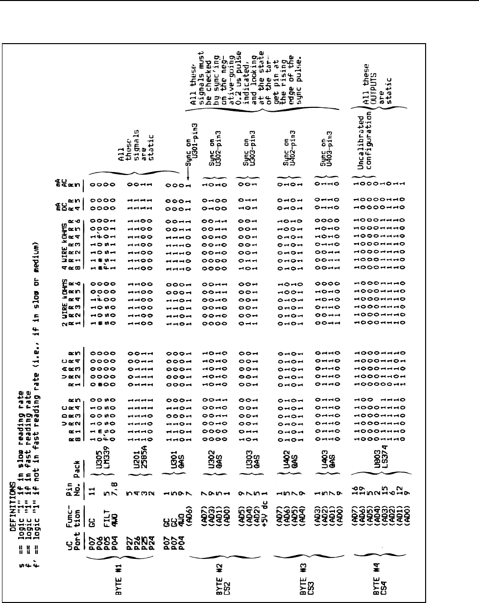
Maintenance
TROUBLESHOOTING
6
6-53
Table 6-21. Analog Control Logic States
t6-21.wmf
Next move to U305-5 and repeat. The slow reading rate gives the following pattern at
U305-5:
111111 00000 111000 1111000 000
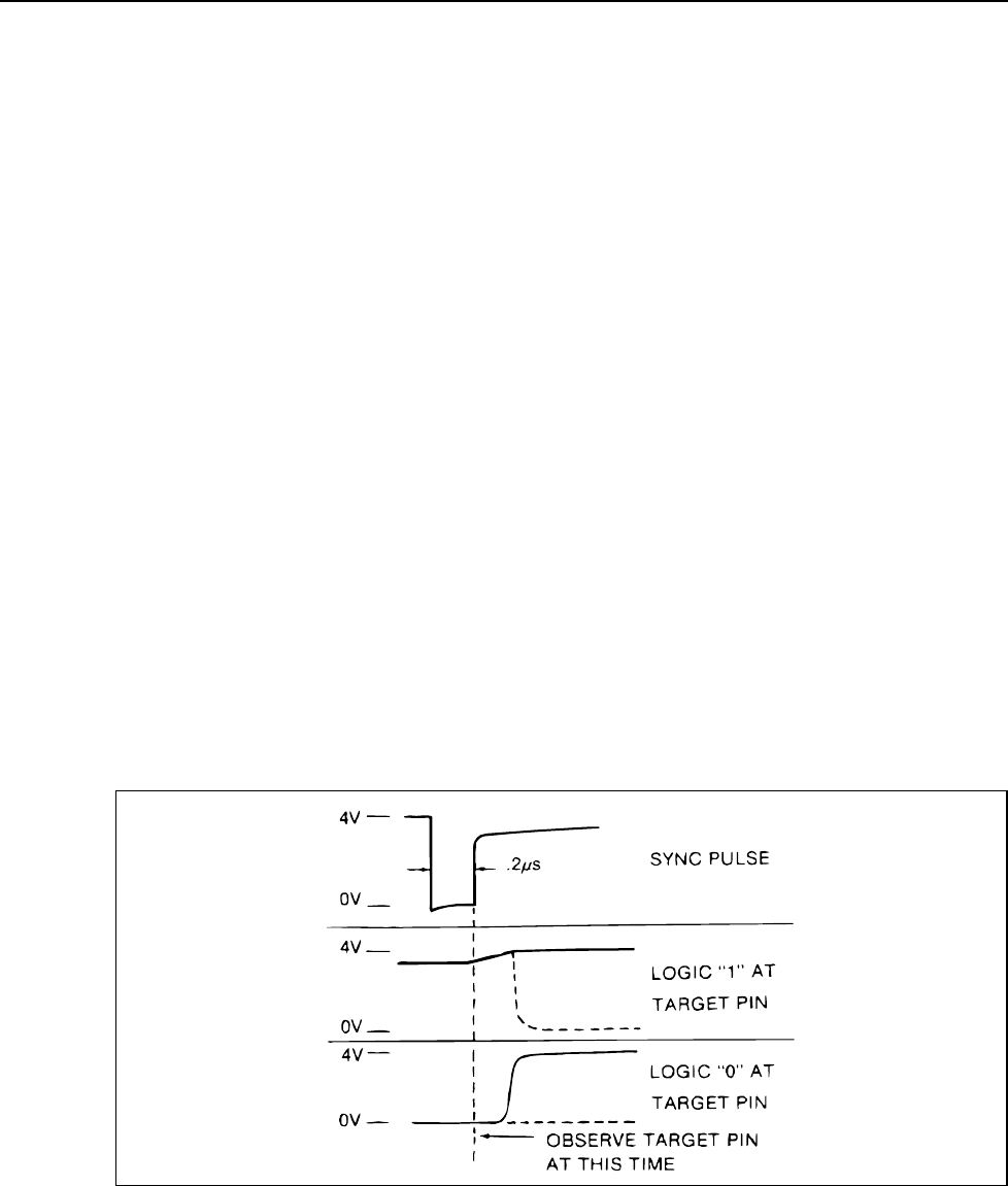
8842A
Instruction Manual
6-54
If the instrument is not in the slow reading rate, it gives the following pattern at U305-5:
000000 00000 000000 0000000 000
Next move to U305-7 and repeat. The pattern at U305-7 will be:
000000 00000 000000 1111111 000
6-61. Evaluating Dynamic Signals
The procedure for evaluating the dynamic signals is only slightly more involved. For
example, consider U302-7 in Table 6-21. At the right end of that row the table says to
sync on U302-3. The sync pulse is negative-going. Apply it to channel 1 of a dual-trace
scope syncing on the leading (negative-going) edge. Observe the target pin (U302-7) on
channel 2 of the scope. While stepping through the 24 ranges observe the state of the
target pin exactly when the sync pulse goes from low to high. (See Figure 6-12.) (This
procedure works best in the fast reading rate since the repetition rate of the sync pulse on
U302-3 is greater.) Using this procedure, the following pattern should be seen:
00000 11111 000000 000000 0 1
Note that the last eight rows in Table 6-21 are actually outputs of U803. Therefore,
observing those pins proves not only that the control signals are correct but also that
U803 itself is functioning correctly.
6-62. DC Scaling Troubleshooting
Whenever there is a failure in the DC Scaling circuit, first check the power supply
voltages for all active components. (Supply voltages and pin numbers are listed in Table
6-22.) A test of the bootstrap supplies for U306 is described later under this heading.
After checking the power supplies, use an oscilloscope to check the digital logic input
pins of quad analog switches U301, U302 and U303. These should show digital signals
with high =>+3V and low =<+0.5V.
f6-12.wmf
Figure 6-12. Typical Dynamic Control Signals
Maintenance
TROUBLESHOOTING
6
6-55
Table 6-22. DC Scaling and Track/Hold Supply Voltages
PIN OR DEVICE SUPPLY VOLTAGE PIN OR DEVICE SUPPLY VOLTAGE
U301-6 +5V U303-20 +7.5V
U301-10 0V U303-11 -8.2V
U301-20 +7.5V U304-4 -8.2V
U301-11 -5V U304-7 +7.5V
U302-6 +5V U305-3 +5V
U302-10 0V U305-12 -5.5V(Nom)*
U302-20 +7.5V U307-4 -15V
U302-11 -5V U307-7 +15V
U303-6 +5V Q305,c +30V
U303-10 0V Q306,c -30V
*With 0V input.
In the 20V range, any voltage applied to the HI INPUT terminal (relative to Reference
Low) should be present at U306-3. If it isn’t, trace the voltage from the HI INPUT
terminal to U306-3 to isolate the problem.
To check U306, select the VDC function and the 2V range. Measure the voltage at TP302
while applying first 1V and then 0V (a short) across the HI and LO INPUT terminals. If
1V and then 0V appear at TP302, U306 is probably OK. If not, the problem is in U306 or
its bootstrap supplies (TP301 and TP303).
To check the bootstrap supplies, put the 8842A in the 20V range and measure the voltage
at TP301, TP302, and TP303. TP301 should be 6.3V (nominal) above TP302, and TP303
should be 6.2V (nominal) below TP302. If the bootstrap supplies are operating correctly,
measure the voltage at U306-3 and U306-6 for input voltages of +20V and -20V; if the
voltage at U306-3 differs from U306-6, then U306 is bad.
To check the dc input path after U306, short the HI and LO INPUT terminals and read
the display. If zero is displayed for ranges r3 and r5 but not for r1, r2, and r4, then the
signal path including Q311 and U301B is suspect. To check Q311, apply a 1V dc input in
the 2V range and check that the voltage at the drain and source of Q311 is 1V. If not,
Q311 or its driver is bad. If 1V appears at U301-16, but not at the display, then U301
may be bad.
If zero is not displayed for r3 and r5 with the HI and LO INPUT terminals shorted, then
Z301 or U302D is probably bad.

8842A
Instruction Manual
6-56
6-63. Track/Hold Troubleshooting
If a problem is suspected in the Track/Hold (T/H) circuit, first check the power supply
voltages of all active components. (See Table 6-22.)
Next, check the T/H output waveform at TP103 with an oscilloscope. Set the 8842A to
the VDC function and 2V dc range, apply +1V dc across the HI and LO INPUT
terminals, and trigger the scope from the falling edge of line not-TR (TP201). The
waveform should look like that in Figure 6-13. The circuit may be checked as follows:
1. Short the HI and LO INPUT terminals, and select the 2V dc range.
2. Short U301-14 to ground (Reference Low). The 8842A should read within 10 counts
of zero. (The actual value is not as important as its stability.)
3. Connect U307-6 to U303-18, and monitor the voltage at TP103 using another
multimeter. The 8842A should read about the same as the external multimeter, but
with opposite sign.
If the 8842A fails step 2 but not step 3, then U303 is bad. If the 8842A fails both steps 2
and 3, then the fault is in the A/D Converter or the T/H Amplifier. To tell which, lift the
end of R318 closest to the front panel (connected to U307-6) and apply an input of less
than +2V to TP103. If the A/D Converter is OK, the 8842A will display the applied
voltage with the opposite polarity. (For example, if you apply +1V, it should display -
1V.) The readings may differ by a slight offset.
6-64. Ohms Current Source Troubleshooting
Malfunctions in the ohms functions can be caused by a fault in the Precision Voltage
Reference, Ohms Current Source, or Ohms Protection. Malfunctions can also be caused
by a fault in the DC Scaling circuit which loads the Ohms Current Source.
First check the power-supply levels (see schematic). Then check all digital logic input
pins of the quad analog switches (U402 and U403). These should show digital signals
with high =>+3V and low =<+0.5V.
To determine whether the Ohms Current Source is being loaded down by the DC Scaling
circuit, select the VDC function and connect a 10 kΩ resistor between the collector of
Q404 and ground (Reference Low). (Selecting the VDC function opens K401, and
configures the Ohms Current Source in the 20 kΩ range.) If the voltage across the 10 kΩ
resistor is 1V, then the Ohms Current Source is working (at least in the 20 kΩ range), and
the problem is probably due to a defect in the DC Scaling circuit.
Maintenance
TROUBLESHOOTING
6
6-57
f6-13.wmf
Figure 6-13. Typical Output Waveforms for Track/Hold Circuit (TP103)
To test whether the Ohms Current Source is actually being sourced out the HI and LO
OUTPUT terminals, select the 20 kΩ range and the 2-wire ohms function, connect a 10
kΩ resistor across the HI and LO INPUT terminals, and measure the voltage across this
resistor with another voltmeter. There should be a 1V drop across the resistor.

8842A
Instruction Manual
6-58
If the ohms functions do not work in any range, check the supplies at U401 (+/-15V),
U404 (+30V and -5V), U402 (+15V, +5V, and 0V), and U403 (+15V, +5V, and 0V), and
check the -7V reference at R416. Also, test the Ohms Protection circuitry as follows:
Select the 20 kΩ range and 2-wire ohms function, connect a 10 kΩ resistor to the HI and
LO INPUT terminals, and bypass the protection circuitry by connecting the emitter of
Q402 to the junction of R410 and R309. If a reading of 10 kΩ is displayed, the protection
circuitry is defective. To isolate the problem, successively short each part of the
protection circuitry that is in series with the Ohms Current Source, until the display reads
10 kΩ.
If the ohms functions work in only certain ranges, suspect resistor network Z401 or
analog switches U402 or U403. To test the analog switches, select a defective range and
connect a short across the switches that are supposed to be closed in that range. If the
Ohms Current Source then works, one of the analog switches is probably bad. If the
range still doesn’t work, then Z401 is probably bad.
To test the first stage of the Ohms Current Source, short U402-19 to Reference Low
through a 2 kΩ resistor and check that the voltage across R401 is 7.0V (nominal) and that
the voltage at U401-6 is -4V (nominal). If the voltages are correct, the first stage of the
Ohms Current Source (U401 and Q401) is working. If not, suspect U401 or Q401.
(Under no circumstances should U401-6 ever be positive.)
If the first stage of the Ohms Current Source is working, test the second stage as follows:
1. Select the 20 kΩ range and apply a 10 kΩ input.
2. Check that the voltage between TP403 and U402-16 is +5V.
3. Measure the voltage at U404-6 with respect to ground. If the voltage at U404-6 is
negative, U404 is bad. (Under no condition should U404-6 ever be negative.)
6-65. Precision Voltage Reference Troubleshooting
If there is a failure of the Precision Voltage Reference, check the power supply levels at
U702. U702 requires two supplies, +15V and -15V, which must be within approximately
+/-5% of their nominal value. Using an oscilloscope, check that the power supplies and
op amp outputs (U702-1 and U702-7) are free from ripple and oscillations.
If the supplies are correct, check the output voltage levels at TP701 and TP702. The
voltages should be +7.00000V +/-1000 ppm and -7.00000V +/-250 ppm. Also check that
the reference amplifier output voltage (U702-1) is nominally +6.5V.
If the outputs are grossly out of tolerance (e.g., stuck at +15V or -15V), the most likely
cause is a bad op amp (U702) or open resistor network (Z701 or Z702). If the outputs are
slightly out of tolerance, the most likely cause is a defective or out-of-tolerance resistor in
Z701 or Z702. Because Z701 is precisely matched with U701, Z701 and U701 must be
replaced as a matched set.
Shorts between lands or runs can also cause small errors (10 ppm to several hundred
ppm). Shorts between sense and output lands can cause small errors that are not related to
resistor networks. Load regulation problems can also be caused by shorts between sense
and load lines.
In some rare cases, the op amps (U702A and U702B) could be out of spec, causing a
small error. The maximum input offset voltage of the op amps used in the circuit is 3 mV.
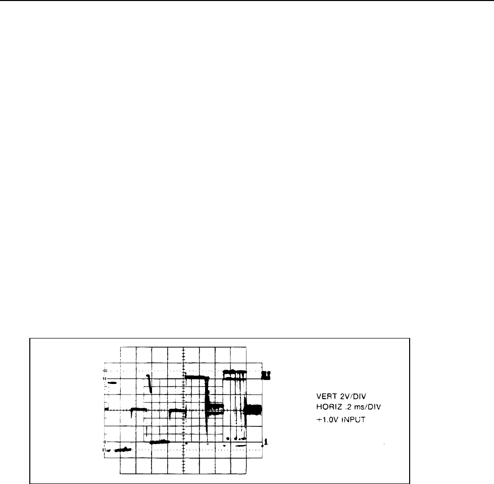
Maintenance
TROUBLESHOOTING
6
6-59
6-66. A/D Converter Troubleshooting
If there is a failure of the A/D Converter, all power supply levels should be checked at the
op amps (U102 and U103) and the A/D IC (U101). The A/D Converter has a total of
seven supplies: +15V, -15V, +5V, +7.5V, -8.2V, +7.00000V, and -7.00000V. All
supplies should be within 5% of their nominal values except for the +7.00000V and -
7.00000V reference supplies, which should be within +/-1000 ppm and +/-250 ppm
respectively. The bootstrap supplies (lines BS1 and BS2) should be +7V and -7V (+/-
10%) referenced to the + input of the A/D amplifier (U103-3).
Troubleshooting the bootstrap supplies can often be made easier by putting the 8842A in
EX TRIG (to stop the A/D Converter) and connecting the input of the A/D Converter
(TP103) to INPUT LO (Reference Low on the schematic). The bootstrap supplies are
then referenced to instrument common (Reference Low).
NOTE
For the following tests, set the 8842A to the VDC function and the 2V
range, and trigger the oscilloscope from the falling edge of line not-TR
(TP201).
If all supplies are correct, the next most useful troubleshooting tool is the A/D output
waveform at TP101, which can be checked with an oscilloscope. The waveform should
look like the one shown in Figure 6-14 when the input voltage is at 50% of the selected
range. Various portions of the waveform correspond to different parts of the A/D cycle.
By examining the waveform, problems in the A/D Converter can be isolated down to one
or two components.
f6-14.wmf
Figure 6-14. Output of A/D Amplifier (TP101)
8842A
Instruction Manual
6-60
f6-15.wmf
Figure 6-15. Waveforms at U101-24 and U101-25
f6-16.wmf
Figure 6-16. Typical Bus Data Line Waveform
The waveform at the storage capacitors can often be used to locate leakage problems. The
leakage can be due to contamination on the Main PCA or to defective switches in U101.
Figure 6-15 shows the waveforms across storage capacitors C102 and C103 (U101-24
and U101-25, respectively) for a specific input.
The A/D Converter communicates with the In-Guard µC via the internal bus, which also
goes to several other sections of the instrument. What looks like a problem in the A/D
Converter may actually be caused by a problem in another section of the instrument
which is loading down the bus data lines (U101-1, -2, -3, -38, -39, -40). A typical
waveform at one of the data lines is shown in Figure 6-16. One of the data lines can be
loaded down so that the In-Guard µC fails to recognize data sent over that line. If so, the
amplitude of the signal of the bad line would be less than 3V peak-to-peak.
One technique of finding an overloaded or shorted data line is to remove the In-Guard µC
and drive one data line at a time through a 1 kΩ resistor. Measure the voltage drop across
a length of the line. Normally the voltage drop across the line is zero volts (less than 5
µV). Voltage drops larger than 5 µV indicate a short. (The voltage drop is caused by
excessive current flowing through the line.)
When troubleshooting the A/D Converter it may be desirable to determine what the
reading is at the A/D Converter when the display is definitely incorrect. A digital

Maintenance
TROUBLESHOOTING
6
6-61
problem between the A/D Converter and the In-Guard µC can cause erroneous or noisy
readings or offsets. Similar problems may be caused by a failure of the Calibration
Memory (U220) or by bad A/D calibration constants. (To check for bad A/D calibration
constants, clear the calibration memory.)
Readings at the A/D Converter can be determined by interpreting the waveform at the
DAC output (TP102). Waveforms at TP102 for several input levels are shown in Figure
6-18. The A/D reading can be calculated by knowing the weight of each bit and by
weighting each nibble correctly. (The first nibble is weighted 1, the second 1/16, the third
1/16 2 the fourth 1/16 3 etc.) Figure 6-18 shows how to read the A/D output for an input
of 0.66V by interpreting the waveform at TP102 using the first three nibbles.
Troubleshooting the A/D Converter for defective components can be simplified by
setting the circuit in a quiescent state. This can be done by selecting EX TRIG, which
causes all A/D activity to stop. The A/D Converter is then in the autozero configuration,
and the offset of the amplifiers and the various levels in the bootstrap circuits can be
easily measured with a voltmeter. Oscillations at the outputs of the amplifiers and other
abnormal signals can easily be identified with an oscilloscope.
6-67. Power Supply Troubleshooting
If the display does not light up, first check the following:
1. Is the instrument plugged in to an energized outlet providing alternating current at a
frequency of 47 Hz to 440 Hz and a voltage within +/-10% of that selected by the
rear panel line voltage selection switches?
2. Is the POWER switch ON (pushed in)?
3. Is the rear panel fuse blown?
CAUTION
For fire protection, use exact fuse replacement only.
If the rear panel fuse is blown, replace it with a 250V fuse of the proper rating for the line
voltage selected. Use 1/4A slow-blow for 100V and 120V power-line voltage and 1/8A
slow-blow for 200V and 240V power-line voltage. If the fuse keeps blowing, measure the
resistances of the power transformer (T601) windings. They should be within 10% of the
values shown on the schematic. If not, the transformer is probably shorted. Also inspect
the area around the transformer POWER switch and power-cord connector to make sure
there isn’t something shorting out the traces. If the IEEE-488 Interface board is suspected
of causing the problem, it can easily be unplugged. Check the crowbar circuit (CR615
and Q601, and R605). If CR615 or Q601 is shorted or if there is a large amount of
leakage or R605 is open, fuses may continue to blow.
If everything looks OK but the fuse keeps blowing, troubleshooting may be performed by
powering the instrument through a variac, applying only enough line voltage to find the
problem without blowing the fuse. NEVER USE A LARGER FUSE. To do so will only
turn a small problem into a big one.
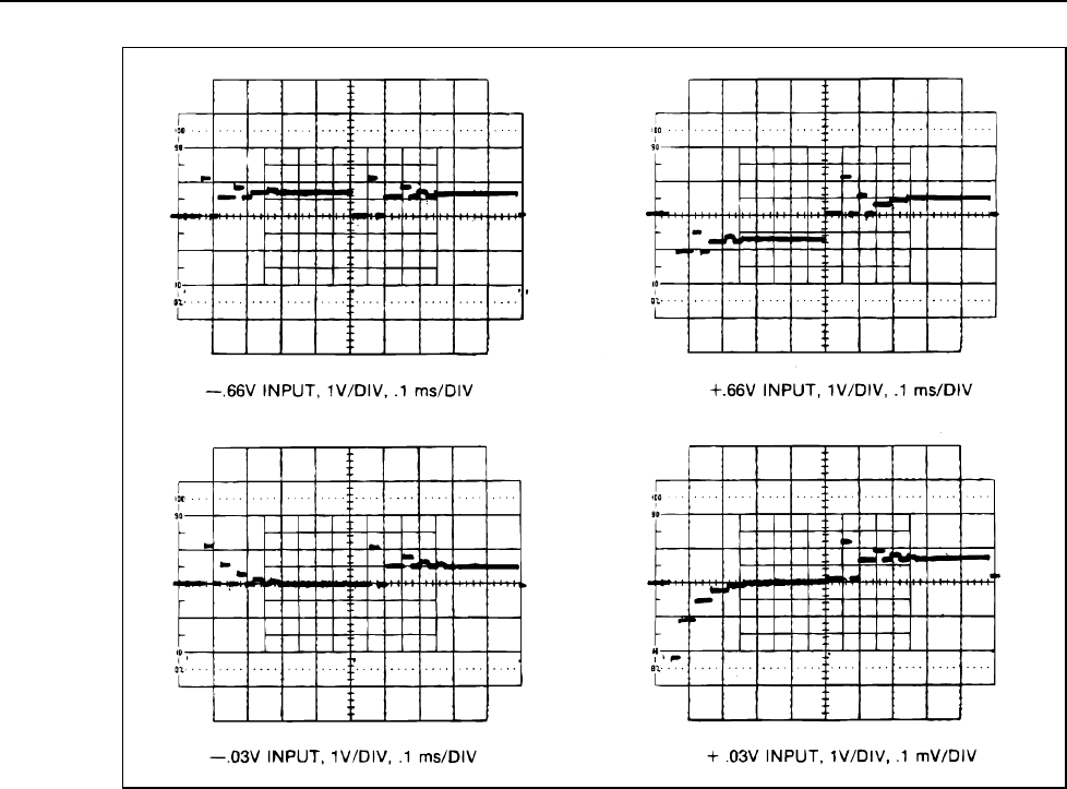
8842A
Instruction Manual
6-62
f6-17.wmf
Figure 6-17. Waveforms at TP102 for Several Inputs on 2V DV Range
Since power supply problems can produce symptoms in many different sections of the
instrument, the first step in troubleshooting any problem should usually be a quick check
of the power supplies. For each power supply (TP801-TP806), check the level with a
voltmeter and check for ripple with an ac-coupled oscilloscope. The dc voltages should
be within the limits given in Table 6-23.
If a supply is too high, either its three-terminal regulator has failed or a fault elsewhere in
the instrument has shorted two supplies together. After repairing such a problem, make
certain that nothing else was damaged by the overvoltage.
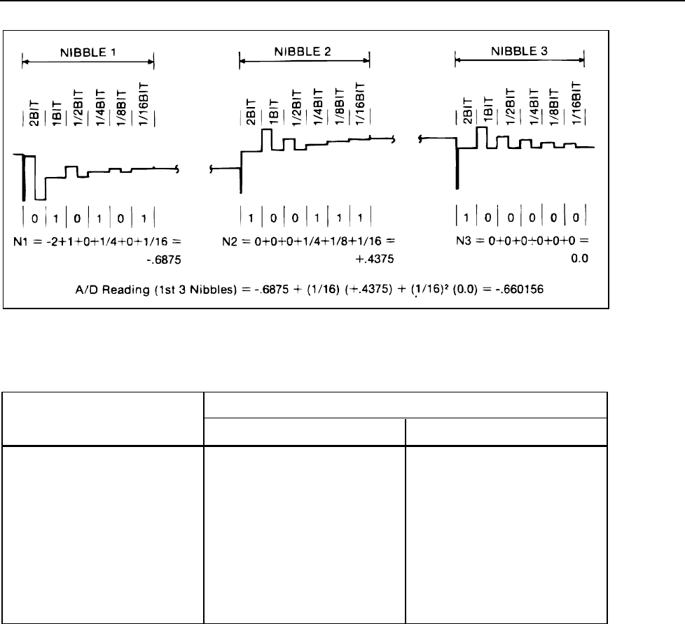
Maintenance
TROUBLESHOOTING
6
6-63
f6-18.wmf
Figure 6-18. Calculating the A/D Reading From TP102 Waveform
Table 6-23. Power Supply Voltages
LIMITS (in volts)TEST POINT
MINIMUM MAXIMUM
+5V 4.75 5.25
+7.5V 7.00 7.87
+15V 14.25 15.75
+30V 28.45 31.55
-8.2 -8.61 -7.60
-15V -15.75 -14.25
-30V -31.55 -28.45
If a supply is too low, there are a number of possible causes. First check the input to the
affected regulator. If it is not at least 1V above the maximum output given in Table 6-23,
the cause may be a bad transformer winding (check the resistance), open or shorted
rectifiers, a shorted filter capacitor, or a shorted regulator. The latter two failures will
usually blow the line fuse.
All regulators incorporate current-limiting which allows them to shut down in the event
of a load failure. Therefore if the power supply output is too low, the first step should be
to determine if it is due to a high load caused by a failure elsewhere in the instrument.
Frequently the faulty component can be found by using a multimeter with at least 5 digits
resolution to check the supply pins of all components powered from that supply. Connect
one lead of the voltmeter to the appropriate test point for the power supply under test and
use the other lead to probe the loads. Small voltage drops across the PCA traces can be
detected in this way, and the fault isolated. If any component other than one of the
regulators is too hot to touch, there is something wrong with it or with something
connected to it.

8842A
Instruction Manual
6-64
The True RMS AC PCA, if installed, uses +5V and +/-15V. If there is a problem with
one of those supplies, first disconnect the True RMS AC PCA. If the problem goes away,
troubleshoot the True RMS AC PCA using the procedure given later in this section.
With most power supply problems, the output voltage is too low or too high. More subtle
problems that may be encountered include high ripple or oscillation. If more than 10 mV
of line-frequency ripple exists on one of the power supply outputs, it is usually caused by
the input being too low, causing the regulator to drop out of regulation. It is also possible
(but not likely) that the regulator itself is defective. High-frequency oscillation
(frequently synchronized with the 1 Mhz or 8 Mhz clock) is usually the result of a bad
regulator or output bypass capacitor. A fair amount of high-frequency noise is generally
present on all the supplies, particularly +5V, and should not cause any concern unless the
instrument behaves erratically or the reading is noisy.
6-68. IEEE-488 Interface Troubleshooting (Option -05)
6-69. SERVICE POSITION
To provide easy access to the IEEE-488 Interface PCA and the Main PCA, the IEEE-488
Interface PCA can be placed in the specially provided service position as follows:
1. Remove the case from the chassis according to the Case Disassembly procedure
provided earlier in this section.
2. Release the two nylon latches that hold the IEEE-488 Interface PCA in place by
pulling the latches upward.
3. Position the IEEE-488 Interface PCA vertically as shown in Figure 6-19 and latch it
in place be pressing the two nylon latches into the mounting supports specially
provided on the chassis.
6-70. DIAGNOSTIC PROGRAM
To facilitate troubleshooting, the IEEE-488 Interface provides a diagnostic program
which places the instrument in known configurations. To initiate the diagnostic program,
proceed as follows:
CAUTION
To avoid damage to the 8842A or other equipment, the 8842A
must be disconnected from all other IEEE-488 Interface
instruments while the diagnostic program is running.
1. Ensure the 8842A POWER switch is OFF.
2. Disconnect all cables from the rear panel IEEE-488 connector.
3. Short TP903 to TP905.
4. Power up the 8842A. The 8842A should display ERROR 50. To exit the
troubleshooting mode, open the jumper and cycle the POWER switch from off to on.
Once the diagnostic program is started, rear-panel IEEE-488 address switches A3, A2,
and A1 can be used to select one of four diagnostic modes, as shown in Table 6-24. In
this table, Configuration indicates which Out-Guard µC I/O port bits are programmed as
outputs and driven with a signal, as shown in Table 6-25.
Maintenance
TROUBLESHOOTING
6
6-65
f6-19.wmf
Figure 6-19. Option -05 Service Position
Table 6-24. Diagnostic Modes
SWITCHES
A3 A2 A1 CONFIGURATION
1 0 1 Static, odd-port bits = 1, even-port bits = 0
1 1 1 Static, odd-port bits = , even-port bits = 1
1 X 0 Dynamic
0 X x Read/Write
NOTES:
• “x” means switch setting does not matter.
• “Static” means the Out-Guard µC I/O port bits programmed as outputs are driven to a constant
logic 1 or 0 level (as determined by switch A2).
• “Dynamic” means the Out-Guard µC I/O port bits programmed as outputs are driven with a 610
Hz, 50% duty cycle square wave. All odd port bit numbers are 180 degrees out of phase with
even port bit numbers.
• “Read/Write” means that data is read from and written to the NEC7210 IEEE chip (U901) when DS
(U901-8) is low. R/W (U901-7) determines whether the data is being read from or written to the
NEC7120. The address bits are always 3 (0011) and the data bits are incremented each time.
8842A
Instruction Manual
6-66
Table 6-25. I/O Port Configurations
CONFIGURATION CONFIGURATION
PORT BIT Static
Dynamic
Read/Write PORT BIT Static
Dynamic
Read/Write
PO-0 OUT Address P1-0 OUT Data
PO-1 OUT Address P1-1 OUT Data
PO-2 OUT Address P1-2 OUT Data
PO-3 OUT Address P1-3 OUT Data
PO-4 IN IN P1-4 OUT Data
PO-5 IN IN P1-5 OUT Data
PO-6 IN IN P1-6 OUT Data
PO-7 IN IN P1-7 OUT Data
P2-0 IN IN P3-0 IN IN
P2-1 IN IN P3-1 IN IN
P2-2 IN IN P3-2 IN IN
P2-3 IN IN P3-3 IN IN
P2-4 IN IN P3-4 IN IN
P2-5 IN IN P3-5 IN IN
P2-6 IN IN P3-6 Clock Clock
P2-7 IN IN P3-7 serial Serial
NOTES:
• Due to external hardware conflicts, the following bits are NEVER driven by the Out-Guard µC in
ANY diagnostic mode: P0-4,5,6,7; P2 (all bits); P3-1,2,3,4.
• P3-6 is the 4 MHz clock for the NEC7210 IEEE chip (U901).
• P3-7 is programmed as the serial output, and constantly transmits hex 55 every 820 µs at 62,000
baud in all four diagnostic modes. This causes the front panel error message.
6-71. True RMS AC Troubleshooting (Option -09)
6-72. SERVICE POSITION
To provide easy access to the True RMS AC PCA and the Main PCA, the True RMS AC
PCA can be placed in the specially provided service position as follows:
1. Remove the case from the chassis using the Case Disassembly procedure provided
earlier in this section.
2. Release the four nylon latches that hold the True RMS AC PCA in place by pulling
the latches upward. (See Figure 809-1E in Section 8.)
3. Disconnect the red ac input lead from both the True RMS AC PCA and the Main
PCA.
Maintenance
TROUBLESHOOTING
6
6-67
4. Position the True RMS AC PCA vertically as shown in Figure 6-20 and latch it in
place by pressing the bottom two nylon latches into the specially provided mounting
supports on the chassis.
5. Connect the Main PCA ac take-off point (stud connector W301) to the True RMS AC
PCA input (the stud connector labeled AC IN) with a 6-inch jumper (E-Z-Hook 204-
6W-S or equivalent).
6-73. MAJOR PROBLEMS
The signal flow through the True RMS AC option is straightforward, with no feedback
paths between individual stages. This simplifies troubleshooting and often makes it
possible to isolate a single defective stage without removing the instrument cover.
Test the mid-frequency response of the VAC function around 1 kHz. If an accurate
reading can be obtained on at least one range, the rms converter (U802) is working
properly. Test the high-frequency response around 100 kHz. If, after calibration, an
accurate reading can be obtained on at least one range, the digitally controlled filter
(U801, U808, R832, and C826-829) is OK. If some ranges are good and others are bad,
the defective stage may be isolated using Table 6-26. If this table is used, the bad ranges
must correspond exactly to the ranges listed in the first column and all other ranges must
be good.
Most ac troubleshooting can be performed with the shields removed. To remove both
shields, unscrew the Phillips screw on the back of the True RMS AC PCA. The only time
it should be necessary to work on the PCA with the shields in place is when there is
subtle high-frequency (>20 kHz) or low-level (<10 mV) error. In that case, the PCA
should be left in its operating position, and the test points probed from the foil side of the
PCA. Test points are labeled on both sides to facilitate such troubleshooting.
Table 6-26. Isolating a Defective AC Stage
DEFECTIVE RANGES DEFECTIVE STAGE
200 mV, 2000 mA U806B
20V, 700V U806A
2V, 200V U806A
200V, 700V Input (Q806, K802, Z801)
2V, 20V, 200V Input (Q806, K802, Z801)
If no ranges work, the signal should be traced from input to output. At any point where
the signal disappears, the preceding stage should be searched thoroughly. To trace the
signal, lock the instrument into one range (200 mV is usually a good choice) and apply
the appropriate voltage shown in Table 6-27 to the HI and LO INPUT terminals. The
input voltage should appear unchanged at pin Z801-1, and should appear at TP801 and
TP802 as shown in Table 6-27. If no ranges work, it is likely that the rest of the scaling
circuitry (U806B) is functional.
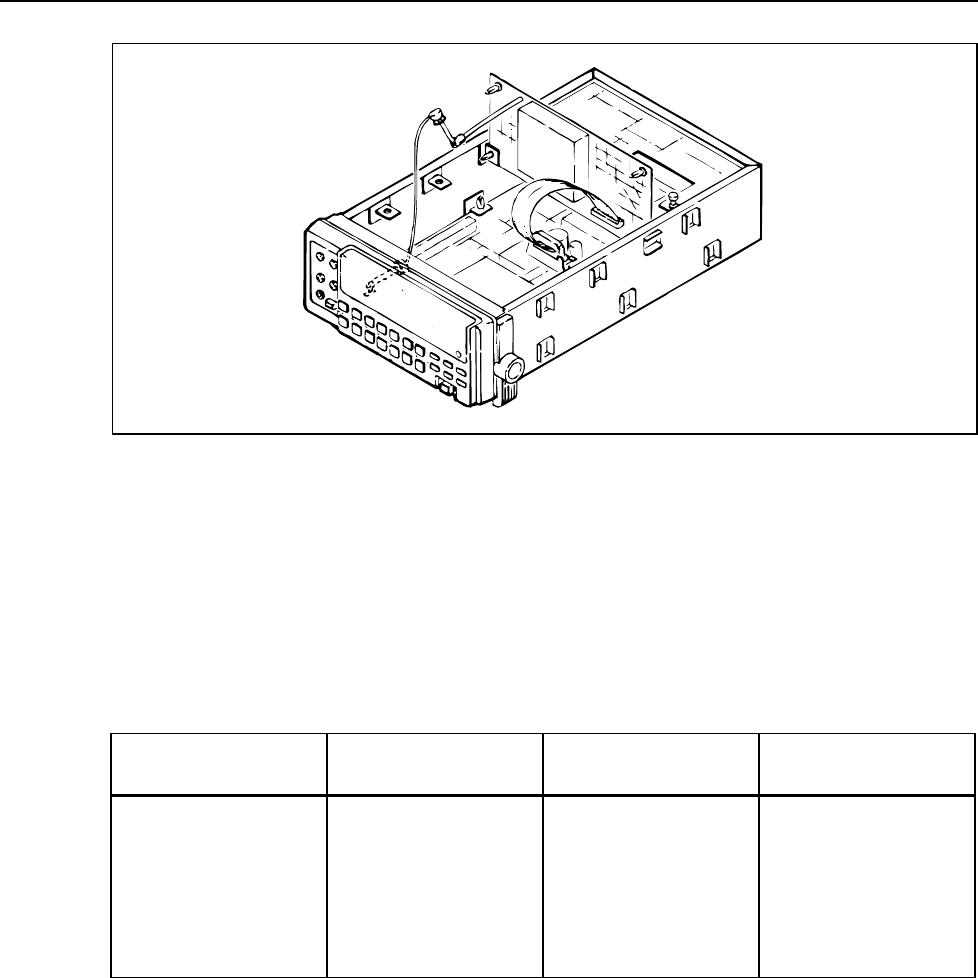
8842A
Instruction Manual
6-68
f6-20.wmf
Figure 6-20. Option -09 Service Position
If the signal at the input to U801A (pin 5) is incorrect, U804 may be defective, or the
switch codes may be wrong. If the latter problem is suspected, refer to Table 6-28 and
test the control lines to U804 (U804-1, 8, 9, 16). If a logic error is found, it may be due to
excessive loading or a faulty data latch (U803), or other cabling or main-board digital
problems. High-frequency oscillation problems are usually caused by switches being on
when they should be off, resulting in positive feedback loops being closed around
portions of the scaling circuitry.
Table 6-27. AC Signal Tracing
RANGE INPUT VOLTAGE (1
kHz)
VOLTAGE AT TP801 VOLTAGE AT TP802
200 mV 100 mV 20 mV 1 V
2V 1V 200 mV 1 V
20V 10V 2V 1V
200V 10V 20 mV 100 mV
700V 100V 200 mV 100 mV
If the signal at TP802 is incorrect, but U801-5 is OK, the digitally controlled filter section
(U801A and U808) is probably defective.
Maintenance
TROUBLESHOOTING
6
6-69
Table 6-28. Truth Table for U804 and K2
PIN OR DEVICERANGE
U804-1 U804-8 U804-9 U804-16 K2
2000 mA 10110
200 mV 10010
2V 11100
20V 01110
200V 11101
700V 01111
NOTE:
For U804, logic 0 = switch on. Logic 1 is >2.4V; logic 0 is <0.8V.
If the signal at TP802 is correct but the output signal (TP803) is incorrect, the rms
converter is probably the source of the problem. Problems with U802 generally show up
as an identical number of counts displayed in all ranges or as an overrange in all ranges.
First isolate faults in the buffer amplifier (U802A) by ascertaining that the signal at
U802-13 is the same as that at TP802 when each is observed with an ac-coupled
oscilloscope, and that the dc offset at U802-13 is less than 4 mV. It is possible that a
component in the loop filter (U809A and associated passive components) or the post-
filter (U809B and associated passive components) is defective. The dc voltage at U802-6
should be the same as that at TP803 for frequencies above 500 Hz, and should be equal to
the rms value of the input signal.
6-74. MORE OBSCURE PROBLEMS
Slow settling time or excessive jitter for low-frequency inputs is caused by rms converter
loop errors. The cause may be a fault in the rms converter or loop filter.
If the output voltage is stuck at the supply rails, the cause is probably a fault in the rms
converter. A less common cause is op amp oscillation; this can be checked with a scope
at TP802.
If one or more ranges are functional but cannot be calibrated at high frequencies, then
either the digitally controlled filter (U801B, R832, and C826-C829) is defective, or a
defective component elsewhere in the circuit has rendered the response out of calibration
range. (The high-frequency calibration is designed to cover the range of error expected
due to op amp variations, input dividers, PCA tolerances, shielding, etc.). A sweep
generator is useful in troubleshooting difficult frequency response problems.
The calibration control lines to U808 are set by software to store a high-frequency
correction factor for each range. A state table cannot be given for these signals, but
common sense will indicate if they are reasonable. For example, if all lines are at logic 0
for all ranges, something is probably wrong. Suspect U803, U808, or digital hardware on
the Main PCA. If the control signals do indeed change with range, U808 or some part of
the digitally controlled filter (U801B, R832, and C826-C829) may be defective. Even
with the worst possible error in the high-frequency calibration code, the reading should
be within 10% of the correct value at frequencies up to 100 kHz. If the error is larger,
there are analog problems.

8842A
Instruction Manual
6-70
It is safe to force one control line at a time high (+5V) or low (0V) to test the individual
switches in U808. (The on resistance of switches in U808 should be less than 500Ω; the
off resistance should be greater than 10 MΩ.) Forcing the control lines high or low
should cause the reading to change when the voltages in Table 6-27 are applied to the
input terminals at 100 kHz. If only certain ranges cannot be calibrated, refer to Table 6-
26 to find the suspected stage.
6-75. Guard Crossing Troubleshooting
To troubleshoot the Guard Crossing circuit, place the 8842A in the In-Guard
Troubleshooting Mode as described under Digital Controller Troubleshooting, earlier in
this section. This causes the In-Guard µC to send a test pattern to the IEEE-488 Interface
PCA via one-half of the Guard Crossing circuit. You should be able to observe the
waveforms shown in the left half of Figure 6-21.
To troubleshoot the second half of the Guard Crossing circuit, leave the 8842A in the In-
Guard Troubleshooting Mode. This causes the IEEE-488 Interface PCA to send a test
pattern to the In-Guard µC. You should be able to observe the waveforms shown in the
right half of Figure 6-21. The IEEE-488 Interface PCA sends the test pattern in response
to the test pattern sent by the In-Guard µC; therefore, the first half of the Guard Crossing
Circuit (which was tested in the previous paragraph) must be working properly before the
second half can be tested.
6-76. INTERNAL CLEANING
CAUTION
Failures due to electrostatic discharge can be caused by
improper handling of the PCAs and by the use of a vacuum
cleaner with static-inducing brushes. To prevent damage by
electrostatic discharge, observe the precautions described on
the Static Awareness sheet in front of this section.
If visual inspection of the instrument shows excessive dirt build-up in the instrument,
clean the appropriate section using clean, oil-free, low-pressure air (less than 20 psi). If
necessary, remove the option PCAs first.
6-77. Cleaning Printed Circuit Assemblies
If conditions warrant, individual printed circuit assemblies (PCAs) can be cleaned with
water-based commercial cleaning systems such as dishwashers. If such systems are used,
observe the following precautions:
1. Remove all shield covers (applies to the True RMS AC PCA) and socketed ICs.
2. Use Reagent Grade 2 or better water (de-ionized or distilled water) for the final rinse
in geographic areas with exceptionally hard water. During the final rinse, spray or
run the water so that the surface is thoroughly covered to remove all ionized material.
3. Thoroughly dry all PCAs using one of the following methods:
a. Preferably, the PCA should be dried in a low-temperature drying chamber or
infrared drying rack with a temperature range of 49°C to 72°C (120°F to 160°F).
b. If neither a drying chamber nor a drying rack is available, air dry the PCA at
ambient room temperature for at least two days.
A satisfactory cleaning method consists of holding the PCAs under hot running water
until they are clean. Follow this wash with a final rinse. (See consideration 2, above.)
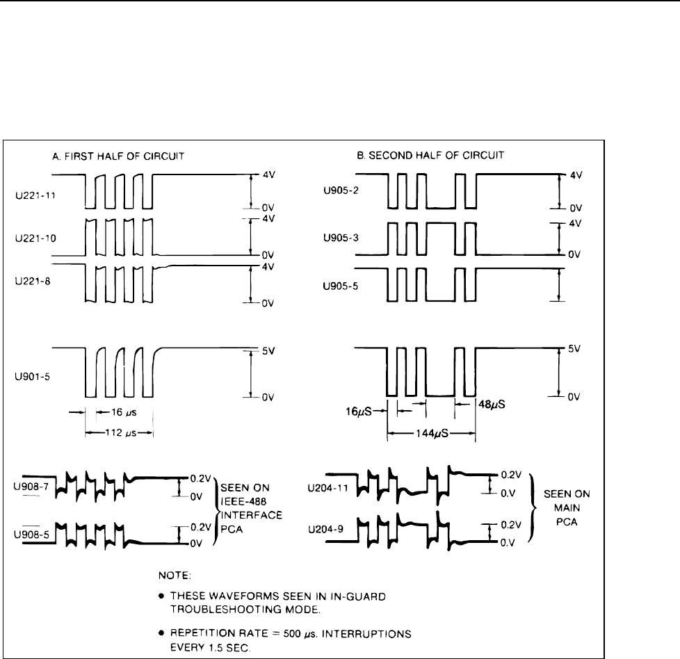
Maintenance
INTERNAL CLEANING
6
6-71
6-78. Cleaning After Soldering
CAUTION
T.M.C. Cleaner and similar products can can attack the nylon
latches and other plastic pieces.
f6-21.wmf
Figure 6-21. Guard Crossing Test Waveforms
If a PCA has been soldered, it should first be cleaned with SPRAYON T.M.C Cleaner
(rosin flux remover) or equivalent. The PCA should then be cleaned with water as
described above.

8842A
Instruction Manual
6-72
7-1
Chapter 7
List of Replaceable Parts
Title Page
7-1. INTRODUCTION................................................................................7-3
7-2. HOW TO OBTAIN PARTS.................................................................7-3
7-3. MANUAL STATUS INFORMATION................................................7-3
7-4. NEWER INSTRUMENTS...................................................................7-4
7-5. SERVICE CENTERS...........................................................................7-4

8842A
Instruction Manual
7-2

List of Replaceable Parts
INTRODUCTION
7
7-3
7-1. INTRODUCTION
This section contains an illustrated list of replaceable parts for the 8842A. Parts are listed
by assembly; alphabetized by reference designator. Each assembly is accompanied by an
illustration showing the location of each part and its reference designator. The parts lists
give the following information:
• Reference designator
• An indication if the part is subject to damage by static discharge
• Description
• Fluke stock number
• Manufacturers supply code (code-to-name list at the end of this section)
• Manufacturers part number or generic type
• Total quantity
• Any special notes (i.e., factory-selected part)
CAUTION
A * symbol indicates a device that may be damaged by static
discharge.
7-2. HOW TO OBTAIN PARTS
Electrical components may be ordered directly from the manufacturer by using the
manufacturers part number, or from the Fluke Corporation and its authorized
representatives by using the part number under the heading FLUKE STOCK NO. In the
U.S., order directly from the Fluke Parts Dept. by calling 1-800-526-4731. Parts price
information is available from the Fluke Corporation or its representatives. Prices are also
available in a Fluke Replacement Parts Catalog which is available on request.
In the event that the part ordered has been replaced by a new or improved part, the
replacement will be accompanied by an explanatory note and installation instructions, if
necessary.
To ensure prompt delivery of the correct part, include the following information when
you place an order:
• Instrument model and serial number
• Part number and revision level of the pca containing the part
• Reference designator
• Fluke stock number
• Description (as given under the DESCRIPTION heading)
• Quantity
7-3. MANUAL STATUS INFORMATION
The Manual Status Information table that precedes the parts list defines the assembly
revision levels that are documented in the manual. Revision levels are printed on the
component side of each pca.

8842A
Instruction Manual
7-4
7-4. NEWER INSTRUMENTS
Changes and improvements made to the instrument are identified by incrementing the
revision letter marked on the affected pca. These changes are documented on a
supplemental change/errata sheet which, when applicable, is included with the manual.
7-5. SERVICE CENTERS
A list of service centers is located at the end of this section.
NOTE
This instrument may contain a Nickel-Cadmium battery. Do not mix with
the solid waste stream. Spent batteries should be disposed of by a qualified
recycler or hazardous materials handler. Contact your authorized Fluke
service center for recycling information.
WARNING
THIS INSTRUMENT CONTAINS A FUSIBLE RESISTOR (PN
733915).TO ENSURE SAFETY, USE EXACT REPLACEMENT
ONLY.
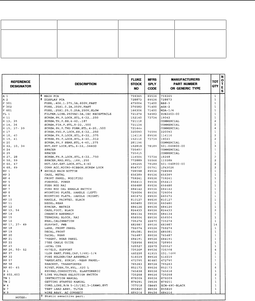
List of Replaceable Parts
SERVICE CENTERS
7
7-5
Manual Status Information
REF OF OPTION NO. ASSEMBLY FLUKE PART NO. REVISION LEVEL
A1
A2
05
09
Main PCA
Display PCA
IEEE-488 Interface PCA
True RMS AC PCA
759365
728873
879267
759266
BE
__
D
N
Table 7-1. 8842A Digital Multimeter
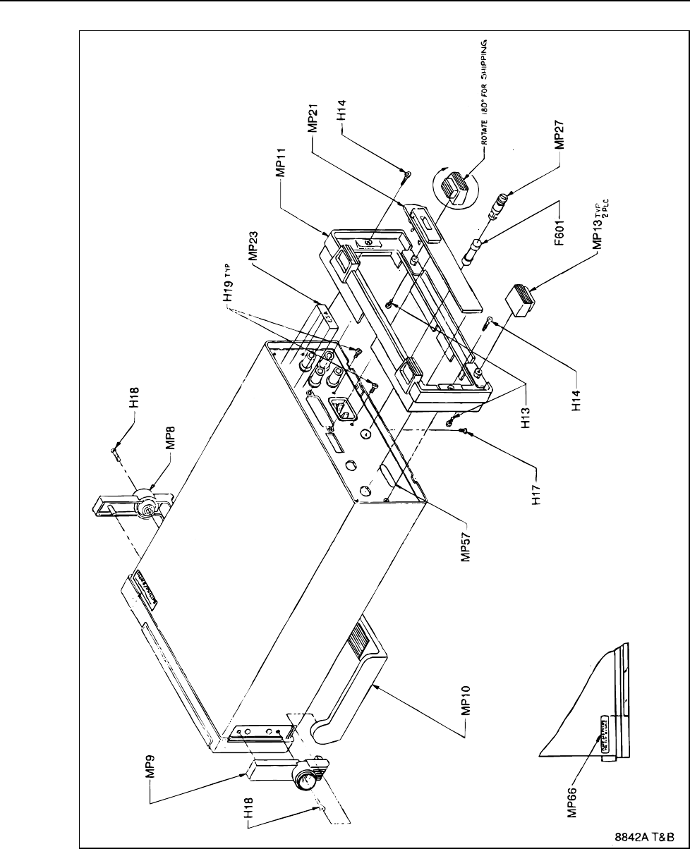
8842A
Instruction Manual
7-6
f7-01_1.wmf
Figure 7-1. 8842A Digital Multimeter
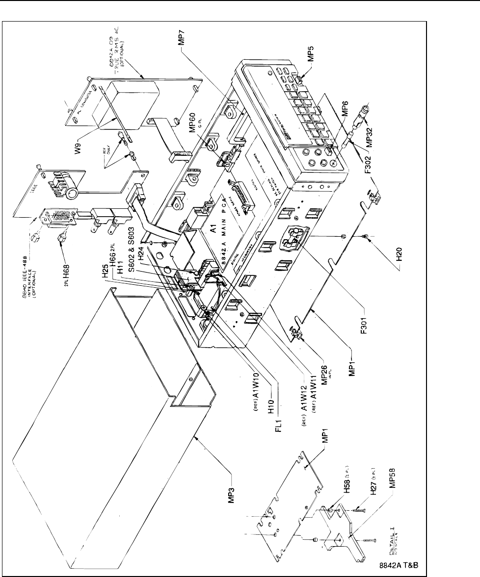
List of Replaceable Parts
SERVICE CENTERS
7
7-7
f7-01_2.wmf
Figure 7-1. 8842A Digital Multimeter (cont)
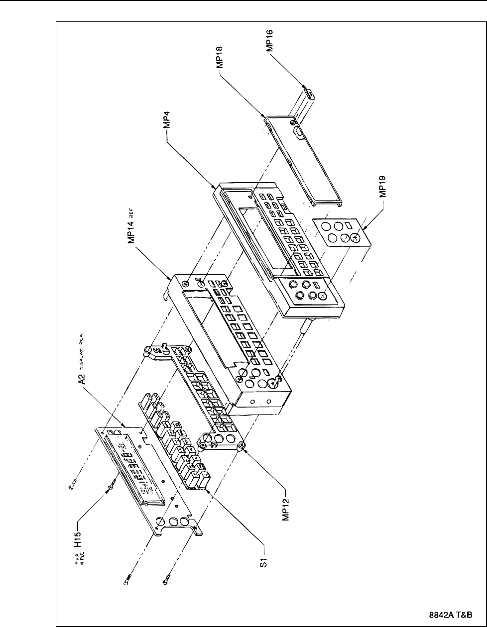
8842A
Instruction Manual
7-8
f7-01_3.wmf
Figure 7-1. 8842A Digital Multimeter (cont)
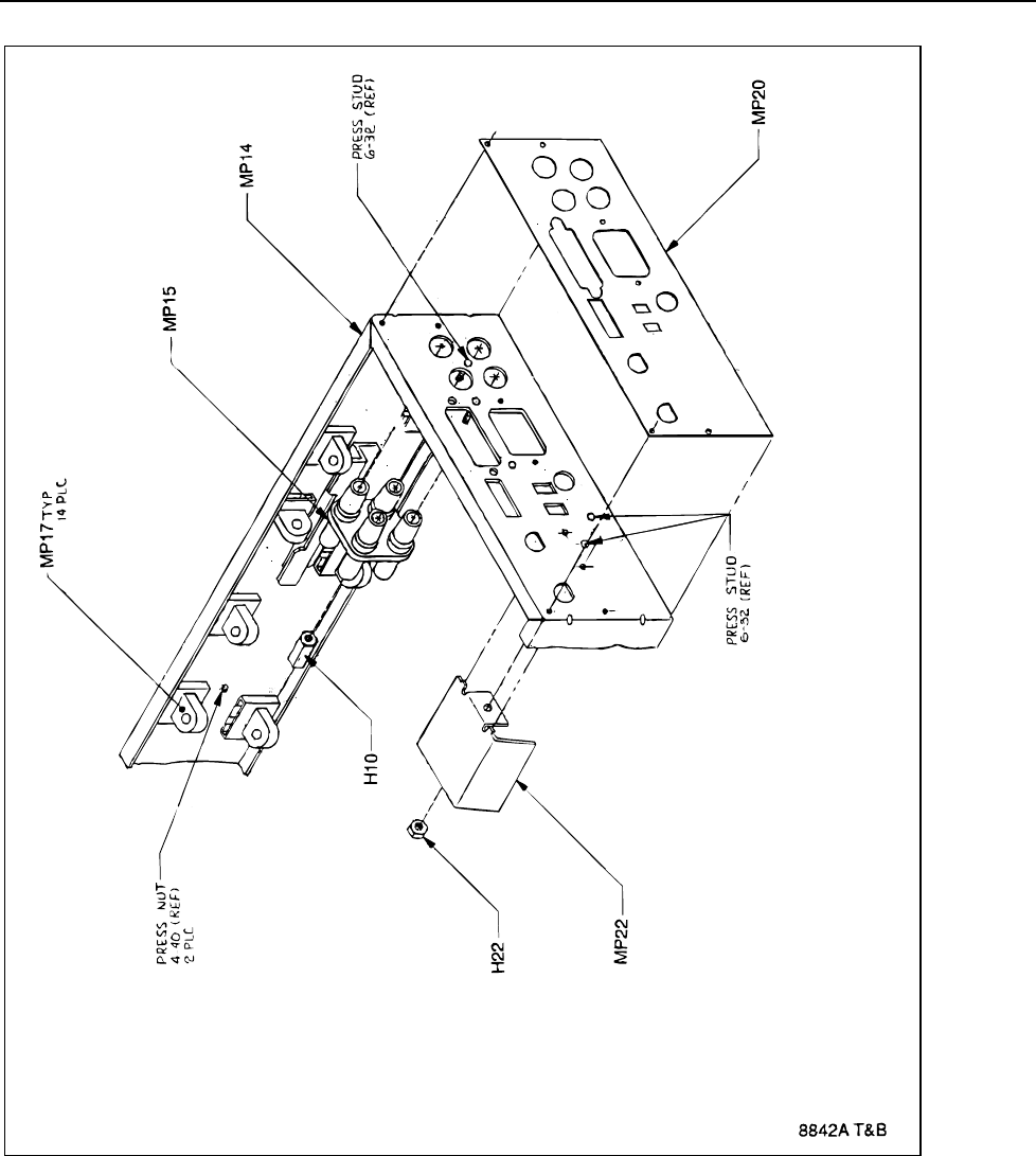
List of Replaceable Parts
SERVICE CENTERS
7
7-9
f7-01_4.wmf
Figure 7-1. 8842A Digital Multimeter (cont)

8842A
Instruction Manual
7-10
Table 7-2. A1 Main PCA
Reference
Designator
Description Fluke Stock
No
Tot Qty Notes
AR701 REF AMP SET 759290 1
C101-103,C311 CAP,POLYPR,0.1UF,+-10%,160V 446781 4
C104,C105,C205- CAP,CER,0.22UF,+80-20%,50V,Z5U 733386 15
209,C304,C305, 733386
C315,C404,C604, 733386
C606,C609,C610 733386
C202,C203,C617, CAP,CER,0.01UF,+80-20%,50V,Z5V 697284 4
C618 697284
C204,C602,C608, CAP,TA,1UF,+-20%,35V 697417 4
C612 697417
C210 CAP,CER,1000PF,+-20%,50V,X7R 697458 1
C301,C302 CAP,POLYPR,0.33UF,+-10%,160V 520346 2
C303 CAP,POLYES,0.33UF,+-10%,50V 715284 1
C306 CAP, POLYPR,0.22UF,+-10%,160V 446799 7
C307 CAP, POLYPR,4700PF,+-10%,63V 721662 t
C308 CAP,POLYPR,0.47UF,+-10%,160V 446807 1
C309 CAP,CER,120PF,+-5%,50V,C0G 721142 1
C310 CAP,CER,120PF,+-5%,50V,C0G 721142 1
C312 CAP,POLYES,0.001UF,+-10%,50V 720938 1
C314 CAP,POLYPR,0.047UF,+-10%,160V 446773 1
C402 CAP,CER,330PF,+-5%,50V,C0G 697441 1
C403 CAP,POLYES,0.47UF,+-10%,50V 697409 1
0601 CAP,AL,6800UF,+/-20%,16V 478784 1
C603 CAP,AL,330UF,+50-20%,100V 484436 1
C605,C607 CAP,AL,470UF,+-20%,50V,SOLV PROOF 747493 2
C611 CAP,AL,100UF,+50-20%,50V 649731 1 1
C701 CAP,CER,270PF,+-5%,50V,C0G 658898 1
CL301 * I-REG DIODE,0.43MA,20%,SEL,TO-0226AC 707836 1
CR101,CR102, ZENER,UNCOMP,3.9V,10%,20.0MA,0,4W 113316 10
CR201,CR202, 113316
CR306,CR307, 113316
CR309,CR311- 113316
313 113316
CR103,CR104, * ZENER,UNCOMP,7.5V,5%,20.0MA,0.4W 256446 3
CR613 * 256446
CR105,CR106, * DIODE,SI,BV=75V,10=150MA,500MW 203323 12
CR203-206, * 203323
CR301,CR302, * 203323
CR401,CR404, * 203323
CR615,CR701 * 203323
CR303 * ZENER,UNCOMP,10.0V,5%,12.5MA,0.4W 246611 1
CR304,CR305 * ZENER,UNCOMP,6.8V,5%,20.OMA,0.4W 260695 2
CR308,CR310 * ZENER,UNCOMP,24.0V,5%,5.2MA,0.4W 267807 2
CR402,CR403 DIODE,SI,1K PIV,1.0AMP 707075 2
CR405 * ZENER,UNCOMP,5.1V,5%,20.0MA,0 159798 1
CR601-606, DIODE,S1,100 PIV,1 AMP 742874 70
CR608-611 742874
CR607,CR612 * ZENER,UNCOMP,6.2V,5%,20.0MA,0.4W 325811 2
CR614 * ZENER,UNCOMP,8.2V,5%,20.0MA,0.4W 386771 1
CR616 ZENER,UNCOMP,56.0V,5%,2.2MA,0.4W 187757 1
CR617 ZENER,UNCOMP,8.2V,5%,20.OMA,0.4W 386771 1
H1,H51 RIVET,S-TUB,OVAL,STL,.118,.156 103424 2
H3 NUT,BROACH,STL,4-40 380196 1
H5 NUT,HEX,STL,4-40 110635 1
H6 SCREW,PH,P,SEMS,STL,6-32,.250 178533 1
H12 SCREW,PH,P,SEMS,STL,4-40,.250 185918 1
J201 HEADER,2 ROW,.100CTR,20 PIN 706986 1
J202 CABLE ASSY,FLAT,10 CONDUCT,6.0 714022 1

List of Replaceable Parts
SERVICE CENTERS
7
7-11
Table 7-2. A1 Main PCA (cont)
Reference
Designator
Description Fluke Stock
No
Tot Qty Notes
J203,J204 CABLE, DISPLAY 684167 2
J602 HEADER,1 ROW,.156CTR,6 PIN 380378 1
JPR001,JPR002 RES JUMPER,0.02,0.25W 682575 2
K301 RELAY,ARMATURE,2 FORM C,5VDC 615575 1
K401 RELAY,REED,1 FORM A,5V,HIGH VOLTAGE 714352 1
MP2 INSUL PT,TRANSISTOR MOUNT,DAP,TO-5 152207 1
MP29,MP50 HLDR,FUSE,13/32,PWB MT 516880 2
MP30 SHIELD, AID 728907 1
MP33 HEAT DIS,VERT,1.18X1.00X0.50,T0-220 414128 1
MP35 HLDR PART,FUSE,BODY,PWB MT 602763 1
MP201 PAD, ADHESIVE 735365 1
Q101,Q309,Q318, * TRANSISTOR,SI,NPN,60V,1W,T0-92 698225 4
Q408 * 698225
Q102,Q319 * TRANSISTOR,SI,PNP,40V,350MW,T0-92 698233 2
Q301, * TRANSISTOR,SI,N-JFET,TO-92 601333 17
Q302,Q303,Q304, * 601333
Q307,Q308,Q310 * 601333
Q311,Q312,Q313, * 601333
Q315,Q316,Q317, * 601333
Q401,Q405-407 * 601333
Q305 * TRANSISTOR,SI,NPN,300V,1W,T0-92 722934 1
Q306,Q402-404 * TRANSISTOR,SI,PNP,350V,0.6W,SEL,TO-92 650846 4
Q314 * TRANSISTOR,SI,N-JFET,DUAL,SEL,TO-71 461772 1
Q320 * TRANSISTOR,SI,N-MOS,350MW,T0-92 783449 1
Q601 * THYRISTOR,SI,SCR,VBO=100V,0.8A 742643 1
R101,R602,R603, RES,CF,1K,+-5%,0.25W 343426 4
R605 343426
R102,R203,R204 RES,CF,470,+-5%,0.25W 343434 3
R103,R104 RES,CF,27K,+-5%,0.25W 441501 2
R105 RES,MF,50K,+-0.1 %,0.125W,25PPM 340257 1
R106 RES,CF,560,+-5%,0.25W 385948 1
R201,R215,R217, RES,CF,15K,+-5%,0.25W 348854 7
R305-307,R604 348854
R202,R315,R327 RES,CF,100,+-5%,0.25W 348771 3
R205,R207,R208, RES,CF,1.5K,+-5%,0.25W 343418 5
R210,R412 343418
R206,R209,R312, RES,CF,33K,+-5%,0.25W 348888 5
R313,R408 348888
R216,R326,R406 RES,CF,2.4K,+-5%,0.25W 441493 3
R301 RES,CC,100K,+-5%,2W 285056 1
R302,R311,R324, RES,MF,46.4K,+-1%,0.125W,50PPM 715185 4
R325 715185
R303 RES,MF,110K,+-1%,0.125W,100PPM 234708 1
R304 FiES,CF,1.5M,+-5%,0.25W 349001 1
R308,R316,R317, RES,CF,1M,+-5%,0.25W 348987 4
R323 348987
R309 RES,MF,1K,+-1%,0.5W,FLMPRF,FUSIBLE 733915 1 1
R310,R409,R415 RES,CF,5.6K,+-5%,0.25W 442350 3
R314 RES,CC,22K,+-10%,2W 109975 1
R318 RES,CF,620,+-5%,0.25W 442319 1
R319 W W RESISTOR 731950 1
R321,R322 RES,MF,10K,+-0.1%,0.725W,50PPM 343459 2
R401 RES, WW, HERM, 1/4W, 54.6K, +-.05% 762120 1
R402 RES,CF,4.3M,+-5%,0.25W 543348 9
R403 RES,CF,10M,+-5%,.25W 875257 1
R407 RES,CF,910,+-5%,0.25W 442335 1
R410 RES,MF,1K,+-1%,100PPM,FLMPRF,FUSIBLE 474080 1 1

8842A
Instruction Manual
7-12
Table 7-2. A1 Main PCA (cont)
Reference
Designator
Description Fluke Stock
No
Tot Qty Notes
R413 RES,MF,4.99M,+-1%,0.125W,100PPM 715060 1
R414 RES,MF,576K,+-1%,0.125W,l00PPM 344291 1
R416 RES,MF,100,+-1 %,0.125W,25PPM 460527 1
R601 RES,CF,560,+-5%,0.25W 385948 1
RV301,RV401-404 VARISTOR,390V,+-10%,1MA 697383 5
RV601 VARISTOR,430V,+-10%,1.0MA 519355 1
S201 SWITCH,PUSHBUTTON,DPDT,PUSH-PUSH 875703 1
S601 SWITCH,PUSHBUTTON,DPDT,PUSH-PUSH 453605 1
T201,T202 TRANSFORMER, PULSE 660589 2
T601 TRANSFORMER, POWER 803270 1
TP101-105,TP201, TERM,FASTON,TA8,.110,SOLDER 512889 25
TP202,TP204-207, 512889
TP301-304,TP401, 512889
TP403,TP601-605, 512889
TP607-609 512889
U102,U702 * IC,OP AMP,DUAL,LO OFFST,VOLT,LO-DRIFT 685164 2
U103 * IC,OP AMP,LO-OFF VOLTAGE,LO-DRIFT 685156 1
U201 * IC,BIPLR,BCHNL DRIVER 685412 1
0203 * IC,LSTTL,HEX INVERTER 393058 1
U204,U305 * IC,COMPARATOR,QUAD,14 PIN DIP 387233 2
U208 * IC,LSTTL,3-8 LINE DCDR W/ENABLE 407585 1
U211 * IC,LSTTL,QUAD 2 INPUT OR GATE 393108 1
0213 * IC,LSTTL,8BIT ADDRSABLE LATCH,W/CLR 419242 1
U215,U217,U218 * IC,BIPLR,8CHNL FLOURSCNT DISPLY DRIVR 685537 3
0216 * IC,LSTTL,BCD TO 7 SEGMENT DCDR/DRVR 697730 1
U219 * IC,CMOS,OCTL D F/F W/3-STATE,+EDG TRG 585364 1
0221 * IC,LSTTL,HEX INVERTER W/SCHMT TRIG 483180 1
U301-303,U402 * IC CMOS, QAS, PLASTIC, HIGH, B GRADE 700013 4
U304 * IC,OP AMP,FET,LO NOISE,PRECISIION,8DIP 780759 1
0306 * IC,OP AMP,SPECIAL,LOW DRIFT,TO-99 650713 1
U307 * IC,OP AMP,JFET IN,COMPENSTD,8 PIN DIP 418780 1
0401 * IC,OP AMP,LO-OFFSET VOLTAGE,LO-NOISE 605980 1
U403 * IC CMOS, QAS, PLASTIC, HIGH, A GRADE 803478 1
U404 * IC,OP AMP,GENERAL PURPOSE,8 PIN 478107 1
VR601 * IC,VOLT REG,FIXED,+5 VOLTS,1.5 AMPS 428847 1
VR602 * IC,VOLT REG,FIXED,+24 VOLTS,1.5 AMPS 604074 1
VR603 * IC,VOLT REG,FIXED,+15 VOLTS,1.5 AMPS 413187 1
VR604 * IC,VOLT REG,FIXED; 15 VOLTS,1.5 AMPS 413179 1
VR605 * IC,VOLT REG,FIXED, 24 VOLTS,1.5 AMPS 418251 1
W1,W8 WIRE ASSEMBLY, GUARD CROSSING 684399 2
W2,W9 WIRE ASSY, GUARD CROSSING 728840 2
W5 HARNESS, ANALOG FRONT 765297 1
W6 HARNESS, ANALOG REAR 765305 1
W10 CABLE, LINE VOLTAGE-GROUND 873740 1
W11 CABLE, LINE VOLTAGE-LINE 873745 1
W12 CABLE, LINE VOLTAGE-NEUTRAL 873752 1
XU101,XU102, SOCKETJC,40 PIN,DUAL WIPE,RET 756668 3
XU212 756668
XU220 SOCKET,IC,24 PIN,DUAL WIPE,BEAM TYPE 756650 1
XU222 756353 1
Y201 CRYSTAL,8.OOMHZ QUARTZ HC-18U 707133 1
Z101 RNET,MF,HERM,SIP,8842 A TO D CONV 755983 1
Z301,Z303 * RNET,MF,HERM,SIP,8842 LO V DIVIDER 755934 2
Z302 * RNET,MF,HERM,SIP,8842 HI V DIVIDER 756130 1
Z304,Z402 * RNET,CERM,SIP,8840 HI V PROTECT 715789 2
Z401 * RNET,MF,HERM,SIP,LO V 1 SOURCE 755884 1
Z702 * RNET,MF,HERM,SIP,8842 LO V DIVIDER 756080 1
1. FUSIBLE RESISTOR. TO ENSURE SAFETY, USE EXACT REPLACEMENT ONLY.
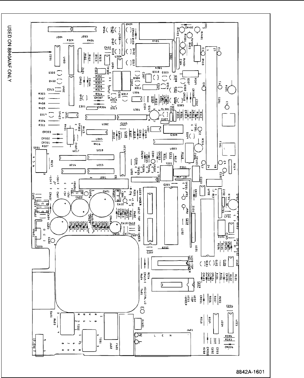
List of Replaceable Parts
SERVICE CENTERS
7
7-13
f7-03.wmf
Figure 7-2. A1 Main PCA
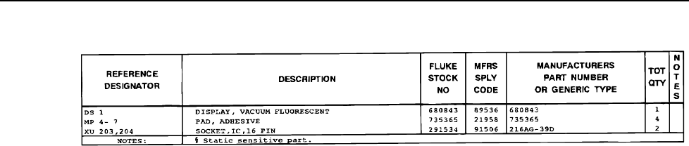
8842A
Instruction Manual
7-14
Table 7-3. A2 Display PCA
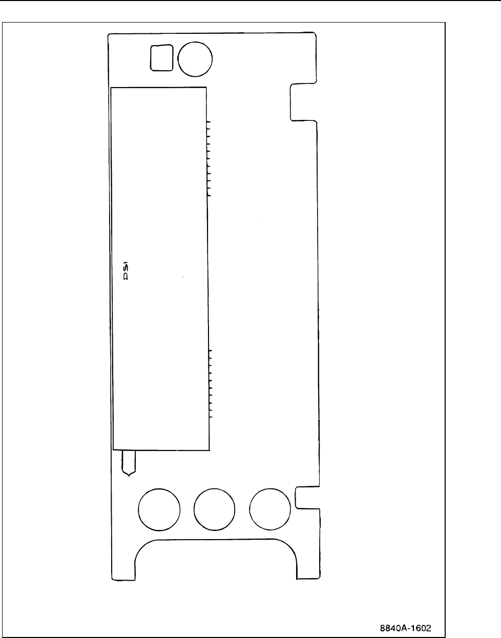
List of Replaceable Parts
SERVICE CENTERS
7
7-15
f7-03.wmf
Figure 7-3. A2 Display PCA
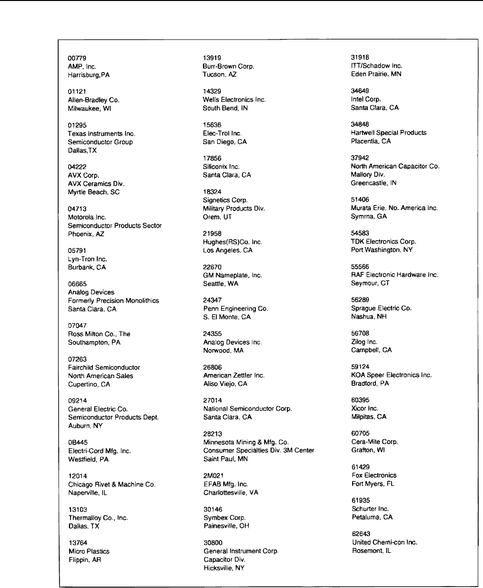
8842A
Instruction Manual
7-16
Supply Codes for Manufacturers
supply_1.wmf
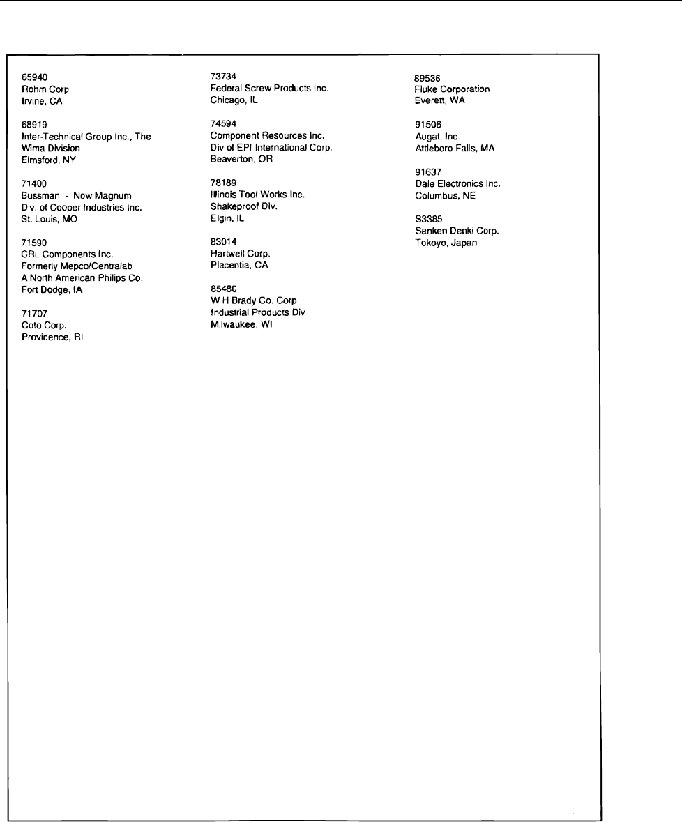
List of Replaceable Parts
SERVICE CENTERS
7
7-17
Supply Codes for Manufacturers (cont)
supply_2.wmf
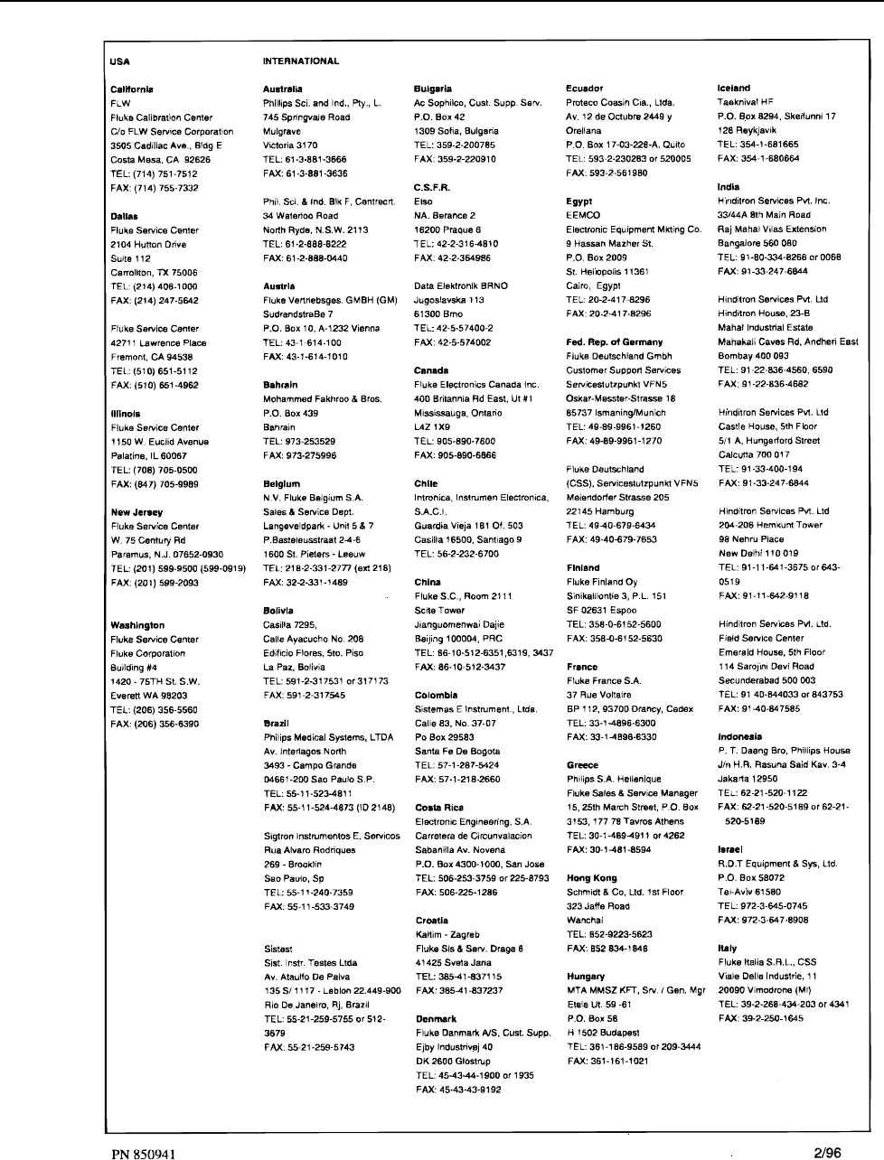
8842A
Instruction Manual
7-18
service_1.wmf
Figure 7-4. Service Centers
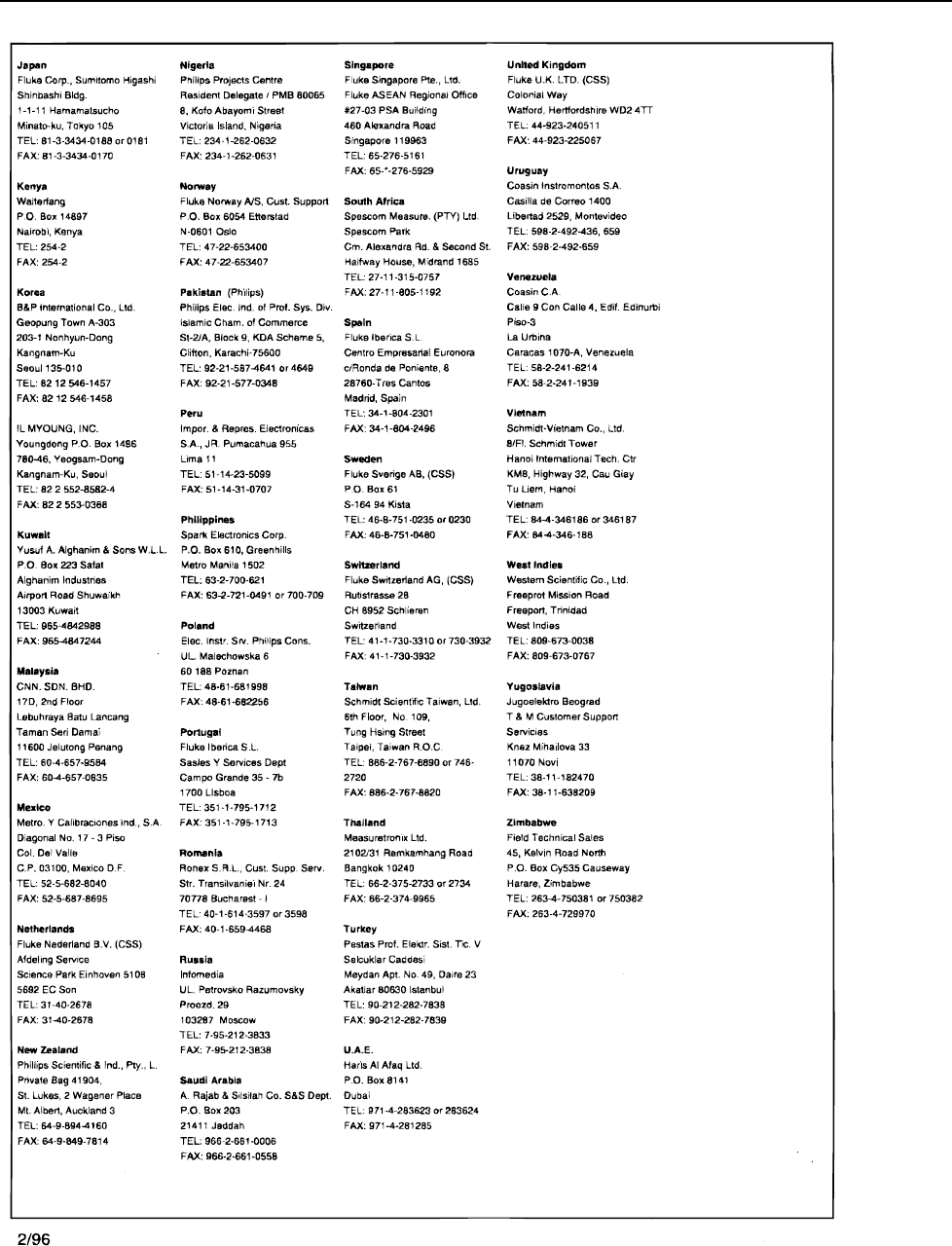
List of Replaceable Parts
SERVICE CENTERS
7
7-19
service_2.wmf
Figure 7-4. Service Centers (cont)

8842A
Instruction Manual
7-20
8-1
Chapter 8
Options and Accessories
Title Page
8-1. INTRODUCTION.................................................................................. 8-3
8-2. ACCESSORIES ..................................................................................... 8-4
8-3. Rack-Mount Kits (Y8834, Y8835 and Y8836).................................. 8-4
8-4. Shielded IEEE-488 Interface Cables (Y8021, Y8022, and Y8023)... 8-4
8-5. Replacement Test Leads (TL70A)..................................................... 8-4
8-6. Deluxe Test Lead Kits (Y8134) ......................................................... 8-4
8-7. Slim-Flex Test Leads (Y8140)........................................................... 8-4
8-8. Temperature Probes (80T-150U, and 80TK.).................................... 8-4
8-9. RF Probes (85RF and 83RF).............................................................. 8-4
8-10. Current Shunt (80J-10)....................................................................... 8-5
8-11. Current Probes (Y8100, Y8101, 80i-400 and 80i-600)...................... 8-5
8-12. High Voltage Probes (80K-6 and 80K-40) ........................................ 8-5

8842A
Instruction Manual
8-2
Options and Accessories
INTRODUCTION
8
8-3
8-1. INTRODUCTION
A number of options and accessories are available which can enhance the 8842A’s
capabilities and increase operator safety. The accessories are summarized in Table 8-1
and described in the following paragraphs. The options are summarized in Table 8-2 and
described in the following subsections.
Table 8-1. Accessories
MODEL DESCRIPTION
Y8021 IEEE-488 Interface Cable (1m)
Y8022 IEEE-488 Interface Cable (2m)
Y8023 IEEE-488 Interface Cable (4m)
Y8834 Single Rack-Mount Kit
Y8835 Dual Rack-Mount Kit
Y8836 Center Rack-Mount Kit
TL70A Replacement Test Leads
Y8134 Replacement Test Leads
Y8140 Slim-Flex Test Leads
80T-150U Temperature Probe
80TK K-Type Thermocouple Converter
85RF RF Probe (100 kHz to 500 MHz)
83RF RF Probe (100 kHz to 100 MHz)
80J-10 Current Shunt
Y8100 Current Probe (200A ac/dc)
Y8101 Current Probe (150A ac)
80I-400 Current Probe (400A ac)
80I-600 Current Probe (600A)
80K-6 High Voltage Probe (6,000V)
80K-40 High Voltage Probe (40,000V)
Table 8-2. Options
NUMBER OPTION
-05 IEEE-488 Interface
-09 True RMS AC

8842A
Instruction Manual
8-4
8-2. ACCESSORIES
Accessories include a variety of rack-mounting kits, cables, test leads, and probes. The
accessories include installation and/or operating instructions.
8-3. Rack-Mount Kits (Y8834, Y8835 and Y8836)
The rack-mount kits allow the 8842A to be mounted in standard 19-inch rack panels. The
Y8834 kit allows the 8842A to be mounted either on the left or the right. The Y8835 kit
allows two 8842As to be mounted side-by-side. The Y8836 kit allows the 8842A to be
mounted in the center of the rack. Installation instructions are given in Section 2, and are
also included with each kit.
8-4. Shielded IEEE-488 Interface Cables (Y8021, Y8022, and Y8023)
Shielded IEEE-488 cables are available in three lengths (see Table 8-1). The cables attach
the 8842A to any other IEEE-488 device. Each cable has double 24-pin connectors at
both ends to allow stacking. Metric threaded mounting screws are provided with each
connector.
8-5. Replacement Test Leads (TL70A)
The TL70A replacement test leads feature safety-designed input connectors.
8-6. Deluxe Test Lead Kits (Y8134)
Each deluxe test lead kit includes two test-tip probes, two alligator clips, two large spade
lug tips, and one spring-loaded hook tip and probe.
8-7. Slim-Flex Test Leads (Y8140)
The Y8140 has adjustable, flexible, and insulated leads, and can fit into small places. The
sharp steel needle points will pierce varnish and thin insulation.
8-8. Temperature Probes (80T-150U, and 80TK.)
The 80T-150U is a universal temperature probe designed to provide virtually any DMM
with temperature measurement capability. The probe provides direct temperature
conversion of 1 mV dc per degree. A three-position switch acts as a power switch and is
used for selecting Celsius or Fahrenheit scaling for the output. The 80TK thermocouple
module converts the microvolt output from a "K" type thermocouple to a 1 mV per
degree signal. The on-off switch allows selection of degrees "C" or "F" output scaling.
8-9. RF Probes (85RF and 83RF)
The RF probes (85RF and 83RF) use the DMM dc volts function to measure radio
frequency (RF) ac signals. The 83RF has a frequency range of 100 kHz to 100 MHz; the
85RF has a frequency range of 100 kHz to 500 MHz. The probes are calibrated so that
the dc output is equivalent to the rms value of a sine wave input over a range of 0.25V to
30V rms.
For best accuracy, the probes should be used with DMMs having 10 MΩ input
impedance. This condition is satisfied by the 8842A in the 200V and 1000V ranges. The
probes can also be used with the 8842A in the 200 mV, 2V, and 20V ranges if a 10 MΩ
resistor is connected in parallel across the 8842A input terminals.

Options and Accessories
ACCESSORIES
8
8-5
8-10. Current Shunt (80J-10)
The 80J-10 current shunt extends ac or dc current measurement up to 10A continuous, or
to 20A for one minute without overheating.
8-11. Current Probes (Y8100, Y8101, 80i-400 and 80i-600)
The current probes extend the ac and dc current measurement range. The Y8100 current
probe uses the Hall effect to measure dc or ac current up to 200A (in two ranges) without
electrical contact. The Y8101 is a low-cost, compact current probe which uses a
transformer to measure ac current from 2A to 150A. The 80i-600 uses a transformer to
measure ac current from 1A to 600A, and features a large jaw opening for industrial use.
The Y8101, 80i-400 and 80i-600 measure ac current only.
8-12. High Voltage Probes (80K-6 and 80K-40)
The high voltage probes extend the dc and ac voltage measurement range while
minimizing shock hazard. The 80K-6 has a range of 0 to 6000V dc or peak ac, with
frequency response to 1 kHz; the 80K-40 has a range of 0 to 40,000V dc or peak ac, with
frequency response to 60 Hz. As the probes use 1000:1 dividers, the probes have a high
input impedance and cause minimal circuit loading. The probes are impedance matched
for both ac and dc measurements. A plastic body protects the operator from the voltage
being measured.
For best accuracy, the probes should be used with DMMs having 10 MΩ input
impedance. This condition is satisfied by the 8842A in the 200V dc and 1000V dc ranges.
The probes can also be used with the 8842A in the 200 mV dc, 2V dc, and 20V dc ranges
if a 10 MΩ resistor is connected in parallel across the input terminals.

8842A
Instruction Manual
8-6
805-1
Chapter 805
Option –05 IEEE-488 Interface
Title Page
805-1. INTRODUCTION................................................................................ 805-3
805-2. CAPABILITIES ................................................................................... 805-3
805-3. EXTERNAL CONTROLS................................................................... 805-3
805-4. INSTALLATION................................................................................. 805-3
805-5. PROGRAMMING INSTRUCTIONS.................................................. 805-4
805-6. MAINTENANCE................................................................................. 805-4
805-7. LIST OF REPLACEABLE PARTS..................................................... 805-4

8842A
Instruction Manual
805-2

Option –05 IEEE-488 Interface
INTRODUCTION
805-3
805-1. INTRODUCTION
The IEEE-488 Interface turns the 8842A into a fully programmable instrument for use
with the IEEE Standard 488-1978 interface bus (IEEE-488 bus). With the IEEE-488
Interface, the 8842A can become part of an automated instrumentation system. The
8842A can be under complete, interactive control from a remote bus controller, or it can
be set to the talk-only mode, connected to a data logger or printer, and dedicated to a
single task.
805-2. CAPABILITIES
The IEEE-488 Interface provides remote control of all front panel controls except for the
POWER, CAL ENABLE, and FRONT/REAR switches. Other features include:
• A simple and predictable command set
• Fast measurement throughput
• Full talk/listen capability, including talk-only operation
• Full serial poll capability, with bit-maskable SRQ
• Full remote/local capability, including local lockout
• External Trigger and Sample Complete connectors
• Remote calibration
• Programmable trigger sources, including two bus triggers
• Informative output suffix (suppressible)
• Selectable output terminators
The 8842A supports the following interface function subsets: SH1, AH1, T5, L4, SR1,
RL1, DC1, DT1, E1, PP0, and C0.
805-3. EXTERNAL CONTROLS
When the IEEE-488 Interface is installed, the rear panel contains EXT TRIG (External
Trigger) and SAMPLE COMPLETE connectors. These controls can be used even when
the 8842A is disconnected from the IEEE-488 bus. Refer to Section 2 for details.
805-4. INSTALLATION
The IEEE-488 Interface is contained on a single, easy-to-install printed circuit assembly
(PCA). To install the option, proceed as follows:
WARNING
TO AVOID ELECTRIC SHOCK, DISCONNECT THE POWER
CORD AND ANY INPUT LEADS BEFORE REMOVING THE
INSTRUMENT CASE.
1. Remove the grounding screw from the bottom of the case and remove the two
rear panel mounting screws (Figure 805-1A).
2. Holding the front panel, slide the case and rear bezel off of the chassis (Figure
805-1B). Note: At this point, the rear bezel is not secured to the case.

8842A
Instruction Manual
805-4
3. Disconnect the ribbon cable from the plastic rear panel insert by pulling the tabs
on either side of the ribbon cable connector outward. Pull the ribbon cable
directly toward the front panel (Figure 805-1C).
4. Remove the rear panel insert by releasing the two snap tabs inside the instrument
(Figure 805-1D).
NOTE
The connection on the rear panel insert is used for factory calibration only.
The connector is electrically isolated from all measuring circuitry.
5. Connect the the ribbon cable from the Main PCA to the connector on the IEEE-
488 Interface PCA (Figure 805-1E).
6. Latch the ribbon cable in place as shown in Figure 805-1F.
7. Make sure the heads of the plastic latches are in the extended position.
8. With the component side down, guide the BNC and IEEE-488 connectors
(located on the rear of the IEEE-488 Interface PCA) into the rear panel, and seat
the IEEE-488 Interface PCA on the mounting supports on the chassis (Figure
805-1G).
9. Fasten the IEEE-488 Interface PCA to the chassis by pressing the two plastic
latches into the mounting supports. (See Figure 805-1H.)
10. Secure the IEEE-488 connector to the rear panel with the two screws and
washers supplied.
11. Replace the cover and rear bezel on the chassis and attach the two ear panel
mounting screws.
12. Attach the grounding screw to the bottom of the case.
WARNING
TO AVOID ELECTRIC SHOCK, ENSURE THE GROUNDING
SCREW IS FIRMLY ATTACHED TO THE CASE BOTTOM.
805-5. PROGRAMMING INSTRUCTIONS
Programming instructions are presented in Section 3. That section also explains how to
set up the 8842A on the IEEE-488 bus.
805-6. MAINTENANCE
All service information regarding Option -05 is contained in Section 6. The theory of
operation is contained in Section 5.
805-7. LIST OF REPLACEABLE PARTS
A list of replaceable parts for the IEEE-488 Interface printed circuit assembly (PCA) is
given in Table 805-1. Refer to Section 7 for ordering information.
Caution
The symbol Y indicates a device that may be damaged by static
discharge.
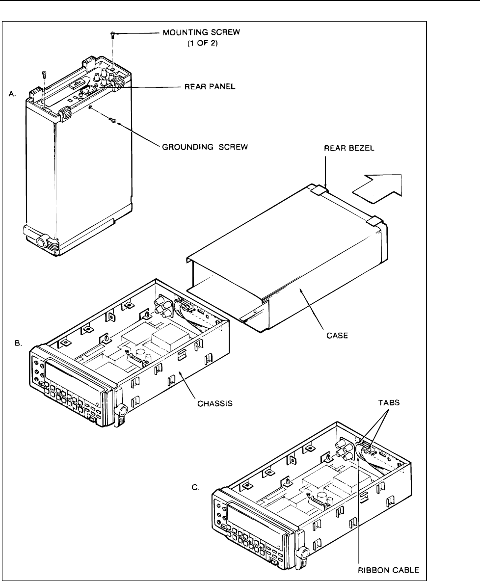
Option –05 IEEE-488 Interface
LIST OF REPLACEABLE PARTS
805-5
f805-1_1.wmf
Figure 805-1. Installing Option -05
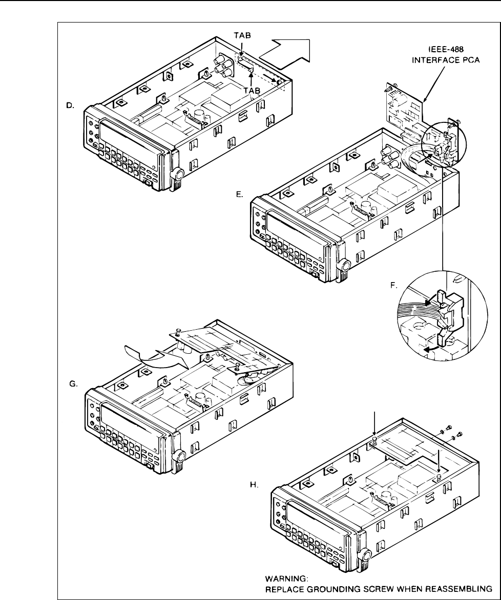
8842A
Instruction Manual
805-6
f805-1_2.wmf
Figure 805-1. Installing Option –05 (cont)
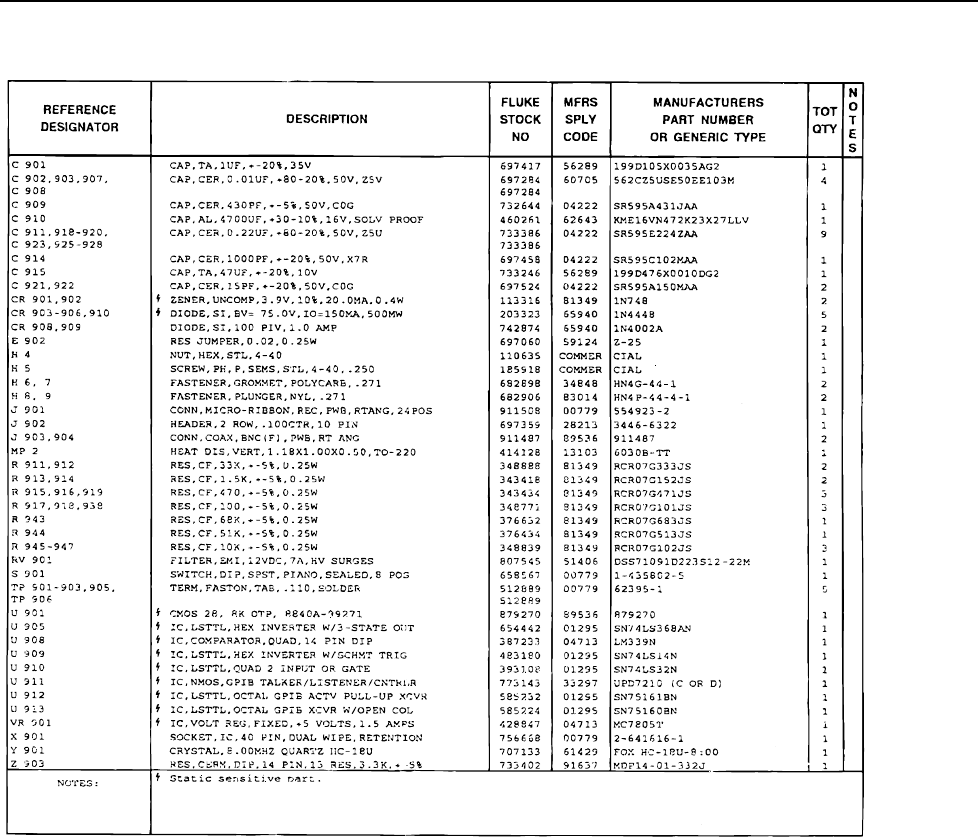
Option –05 IEEE-488 Interface
LIST OF REPLACEABLE PARTS
805-7
Table 805-1. Option -05A IEEE-488 Interface PCA
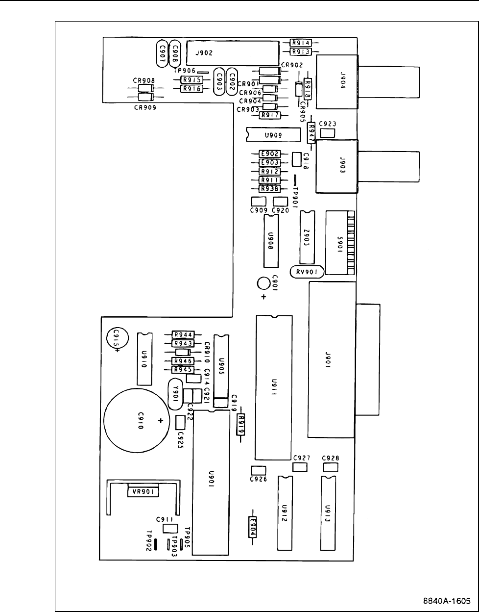
8842A
Instruction Manual
805-8
f805-2.wmf
Figure 805-2. IEEE-488 Interface PCA
809-1
Chapter 809
Option –09 True RMS AC
Title Page
809-1. INTRODUCTION.................................................................................. 809-3
809-2. INSTALLATION................................................................................... 809-3
809-3. OPERATING INSTRUCTIONS............................................................ 809-4
809-4. MAINTENANCE................................................................................... 809-4
809-5. LIST OF REPLACEABLE PARTS....................................................... 809-4

8842A
Instruction Manual
809-2

Option –09 True RMS AC
INTRODUCTION
809-3
809-1. INTRODUCTION
The True RMS AC option gives the 8842A the ability to make ac voltage and current
measurements. The ac functions are selected with the front panel VAC and mA AC
buttons, or by remote commands if the IEEE-488 Interface option is installed.
Specifications for Option -09 are shown in Section 1, Table 1-1.
809-2. INSTALLATION
The True RMS AC option is contained on a single, easy-to-install printed circuited
assembly (PCA). To install the option, proceed as follows:
WARNING
TO AVOID ELECTRIC SHOCK, DISCONNECT THE POWER
CORD AND TEST LEADS BEFORE REMOVING THE
INSTRUMENT CASE.
1. Remove the grounding screw from the bottom of the case and remove the two rear
panel mounting screws (Figure 809-1A).
2. Holding the front panel, slide the case and rear bezel off of the chassis (Figure
809-1B). (At this point, the rear bezel is not secured to the case.)
3. Holding the True RMS AC PCA slightly above the chassis, component side down,
connect the the ribbon cable from the True RMS AC PCA to the Main PCA and
latch it in place. (See Figure 809-1C and D.)
4. Connect the red lead from the True RMS AC PCA to stud W301 on the Main
PCA. (See Figure 809-1C.) The stud is located next to the forward end of the
FRONT/REAR switch.
5. Make sure the heads of the four plastic latches are in the extended position. Guide
the PCA into the 4 circuit board supports.
6. Fasten the True RMS AC PCA to the chassis by pressing the four nylon latches
into the mounting supports on the chassis. (See Figure 809-1E.)
7. Reinstall the cover and rear bezel on the chassis and attach the two rear panel
mounting screws.
8. Attach the grounding screw to the bottom of the case.
WARNING
TO AVOID ELECTRIC SHOCK, ENSURE THE GROUNDING
SCREW IS FIRMLY ATTACHED TO THE CASE BOTTOM.
9. Calibrate the VAC voltage and mA AC functions according to the calibration
instructions given in the Maintenance section.

8842A
Instruction Manual
809-4
809-3. OPERATING INSTRUCTIONS
For operating instructions, refer to Section 2. For ac measurement considerations, refer to
Section 4.
809-4. MAINTENANCE
All service information regarding Option -09 is contained in Section 6. The theory of
operation is contained in Section 5.
809-5. LIST OF REPLACEABLE PARTS
A list of replaceable parts for the True RMS AC printed circuit assembly (PCA) is given
in Table 809-1. Refer to Section 7 for ordering information.
CAUTION
The symbol * indicates a device that may be damaged by static
discharge.
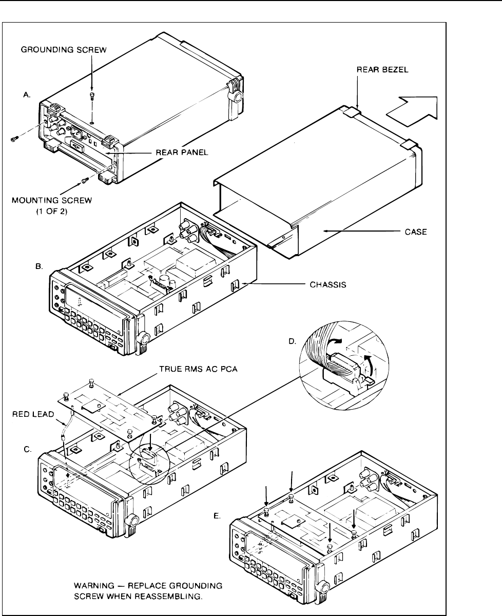
Option –09 True RMS AC
LIST OF REPLACEABLE PARTS
809-5
f809-1.wmf
Figure 809-1. Installing Option -09
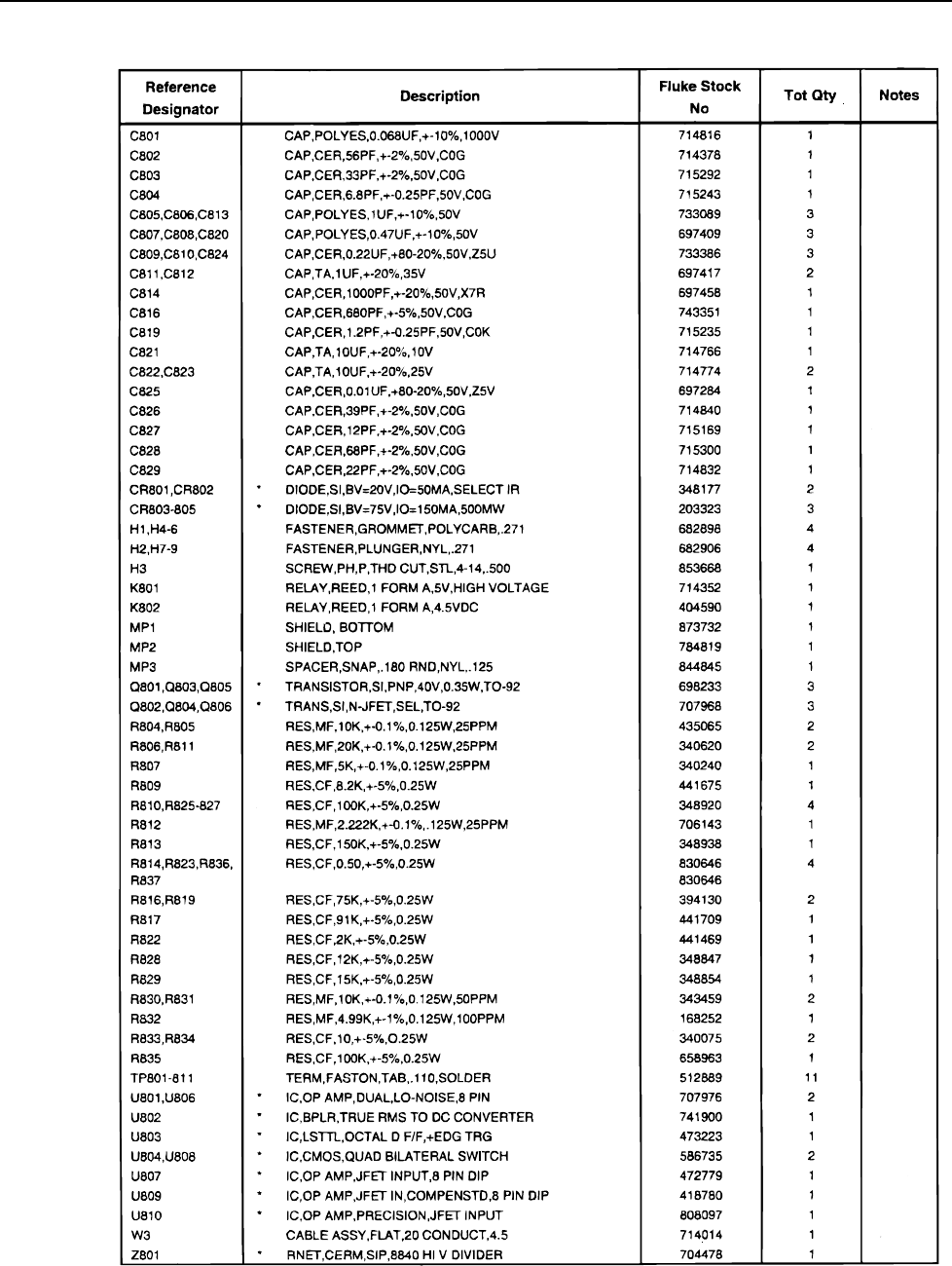
8842A
Instruction Manual
809-6
Table 809-1. Option -09 True RMS AC PCA
t809-1.wmf
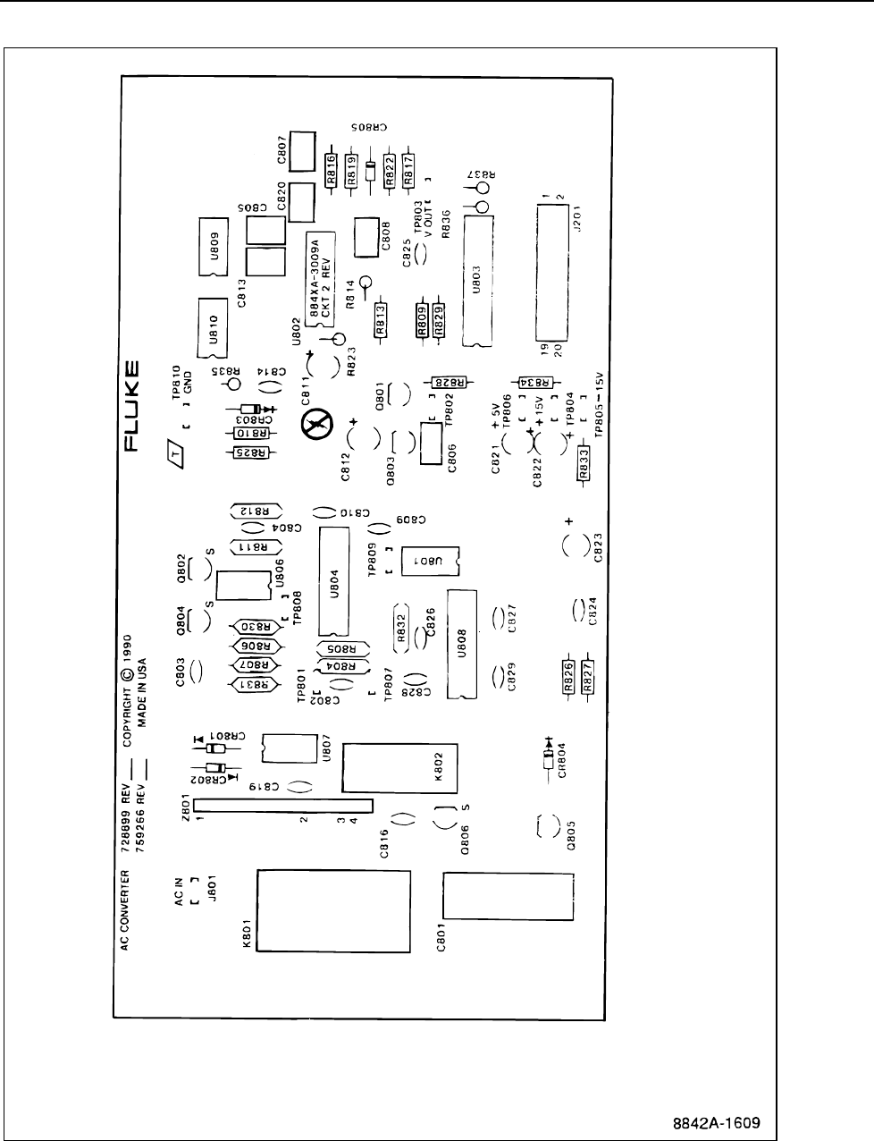
Option –09 True RMS AC
LIST OF REPLACEABLE PARTS
809-7
f809-2.wmf
Figure 809-2. True RMS AC PCA

8842A
Instruction Manual
809-8
9-1
Chapter 9
Schematic Diagrams

8842A
Instruction Manual
9-2
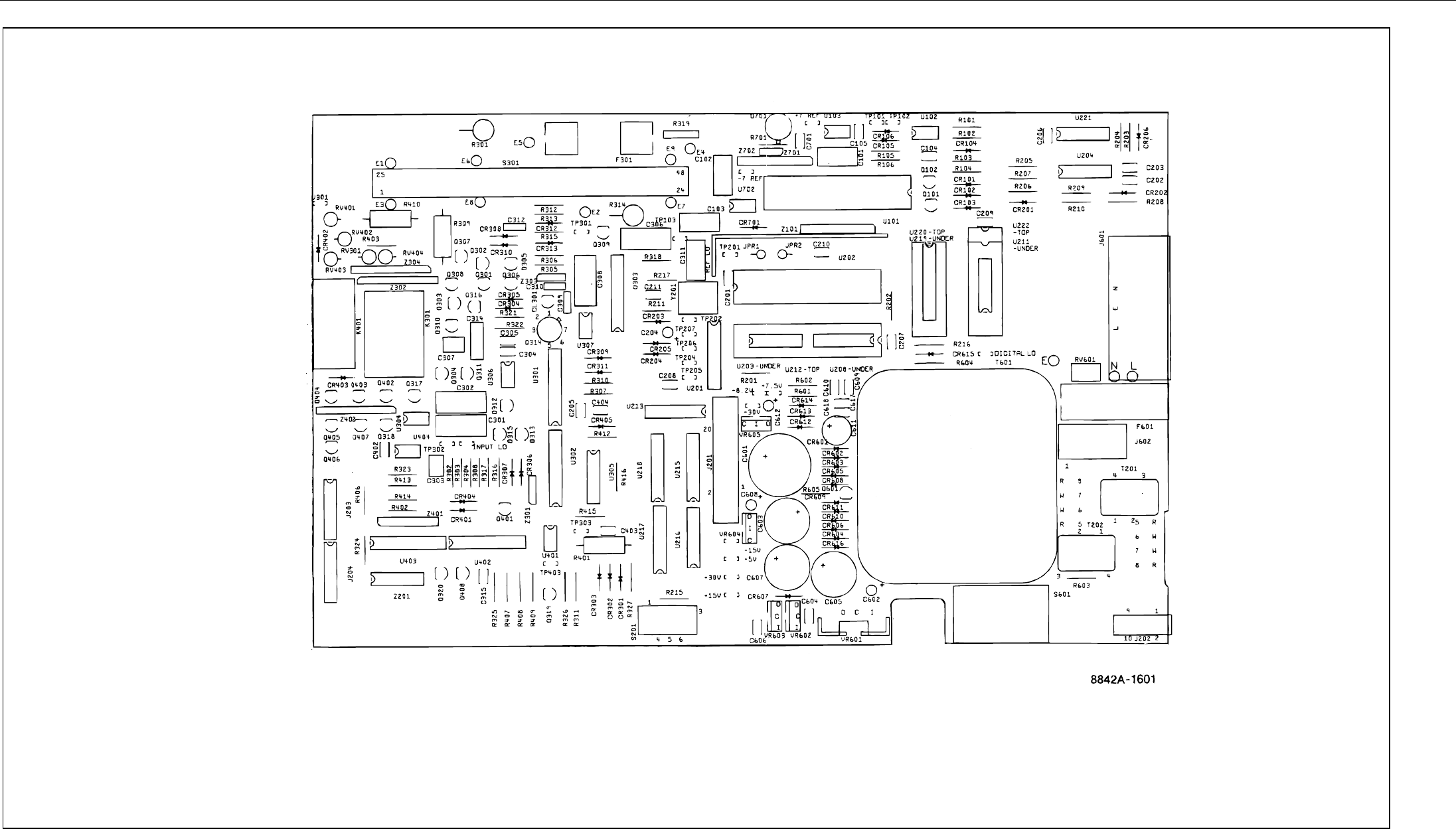
Schematic Diagrams
9
9-3
f9-01_1.wmf
Figure 9-1. Main PCA, DC Scaling and F/R Switch
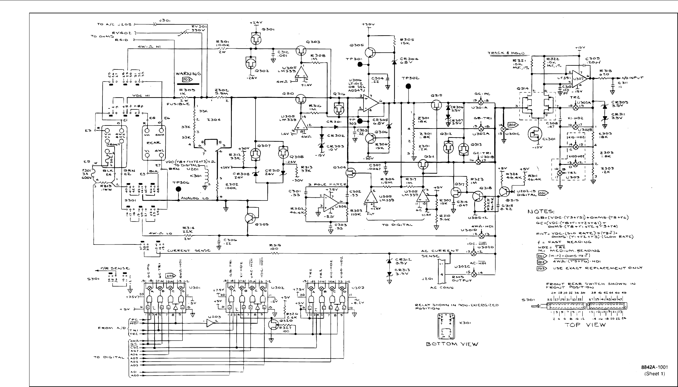
8842A
Instruction Manual
9-4
f9-01_2.wmf
Figure 9-1. Main PCA, DC Scaling and F/R Switch (cont.)
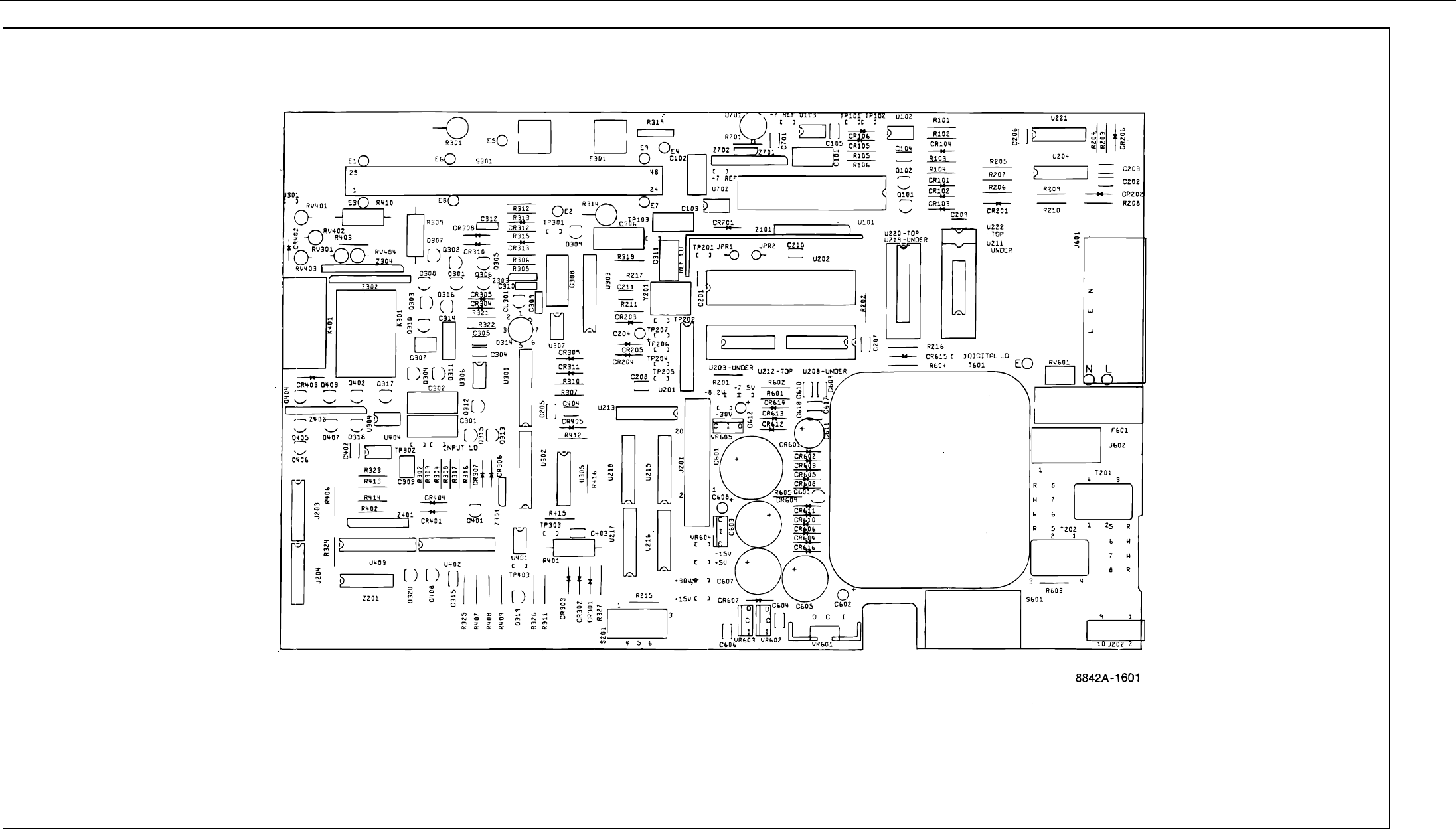
Schematic Diagrams
9
9-5
f9-02_1.wmf
Figure 9-2. Main PCA, A/D Converter
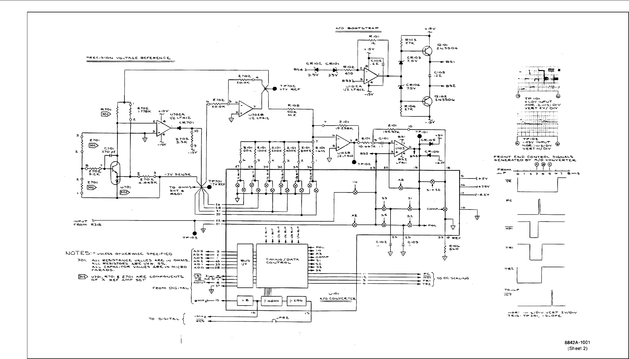
8842A
Instruction Manual
9-6
f9-02_2.wmf
Figure 9-2. Main PCA, A/D Converter (cont.)
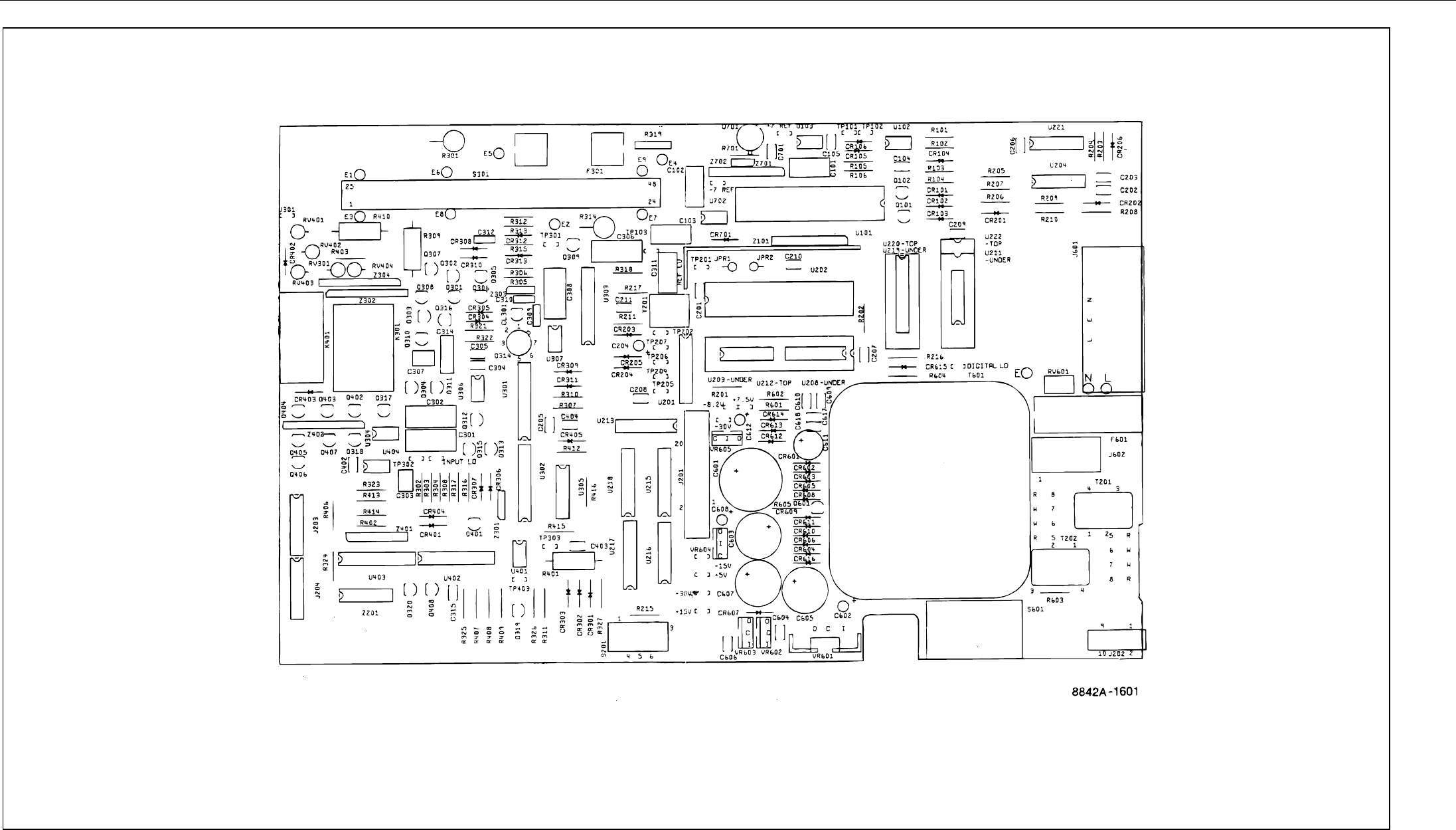
Schematic Diagrams
9
9-7
f9-03_1.wmf
Figure 9-3. Main PCA, Ohms Current Source
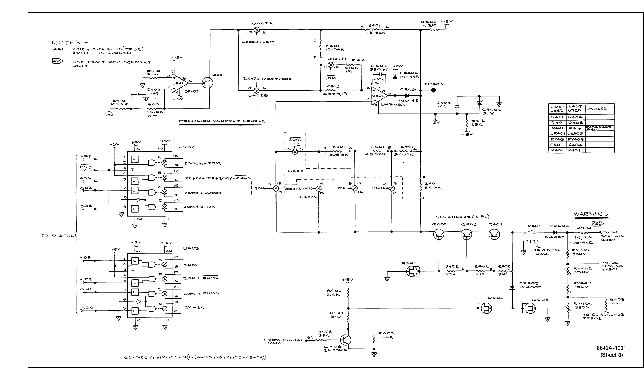
8842A
Instruction Manual
9-8
f9-03_2.wmf
Figure 9-3. Main PCA, Ohms Current Source (cont.)
Schematic Diagrams
9
9-9
f9-04_1.wmf
Figure 9-4. Main PCA, Digital
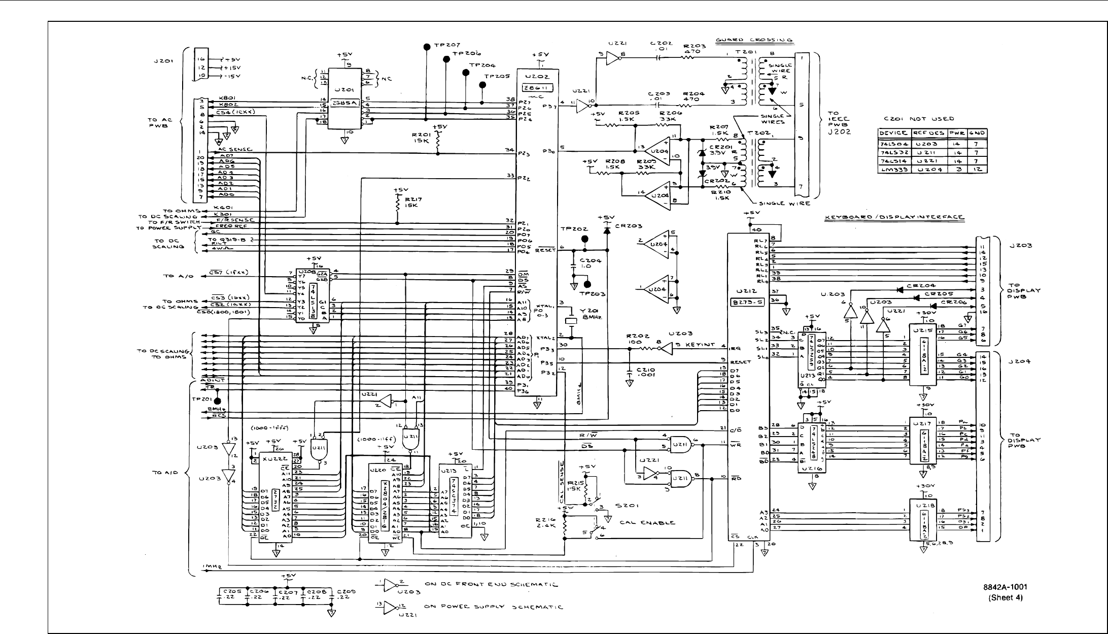
8842A
Instruction Manual
9-10
f9-04_2.wmf
Figure 9-4. Main PCA, Digital (cont.)
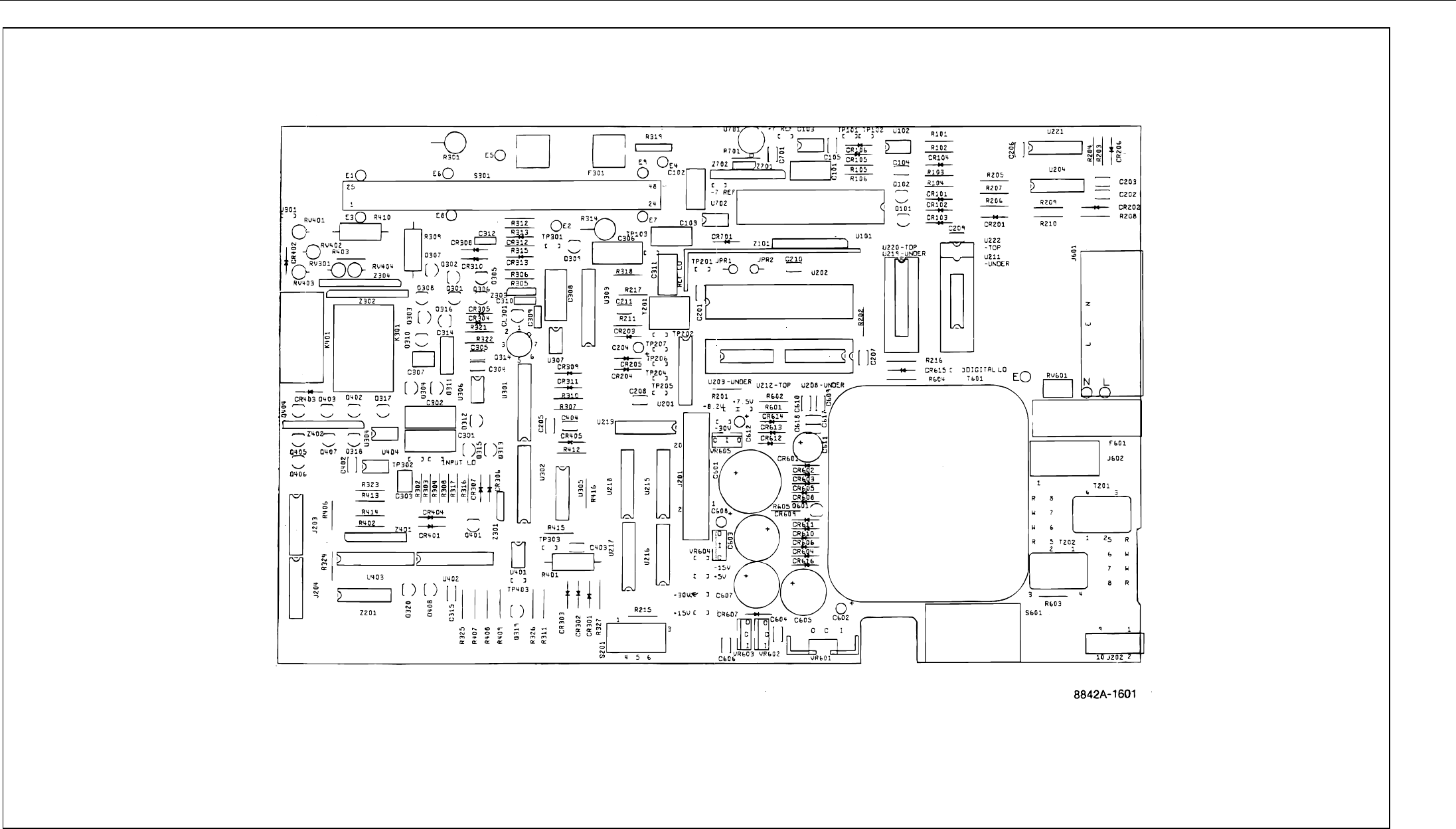
Schematic Diagrams
9
9-11
f9-05_1.wmf
Figure 9-5. Main PCA, Power Supply
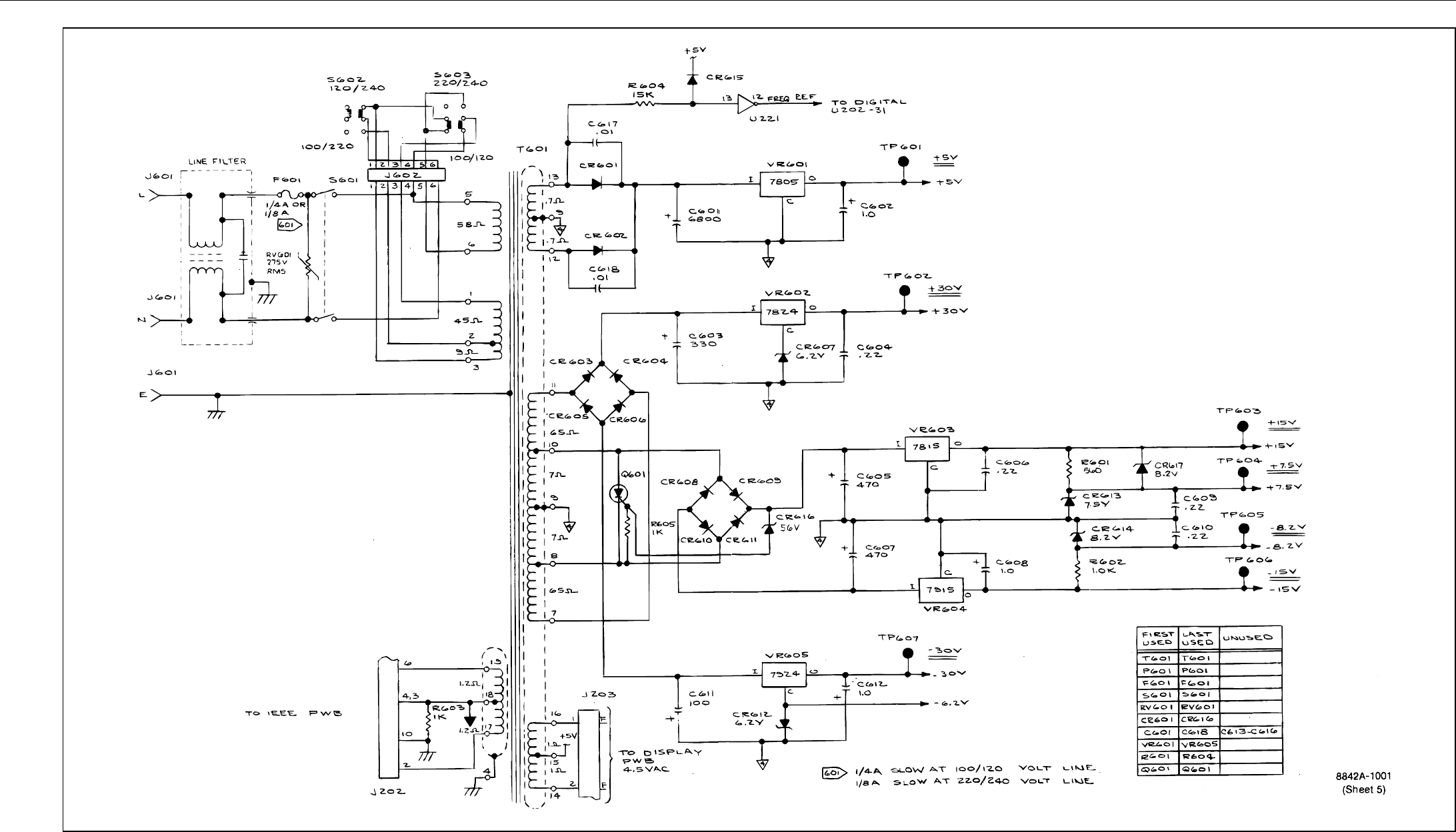
8842A
Instruction Manual
9-12
f9-05_2.wmf
Figure 9-5. Main PCA, Power Supply (cont.)
Schematic Diagrams
9
9-13
f9-06_1.wmf
Figure 9-6. Display PCA
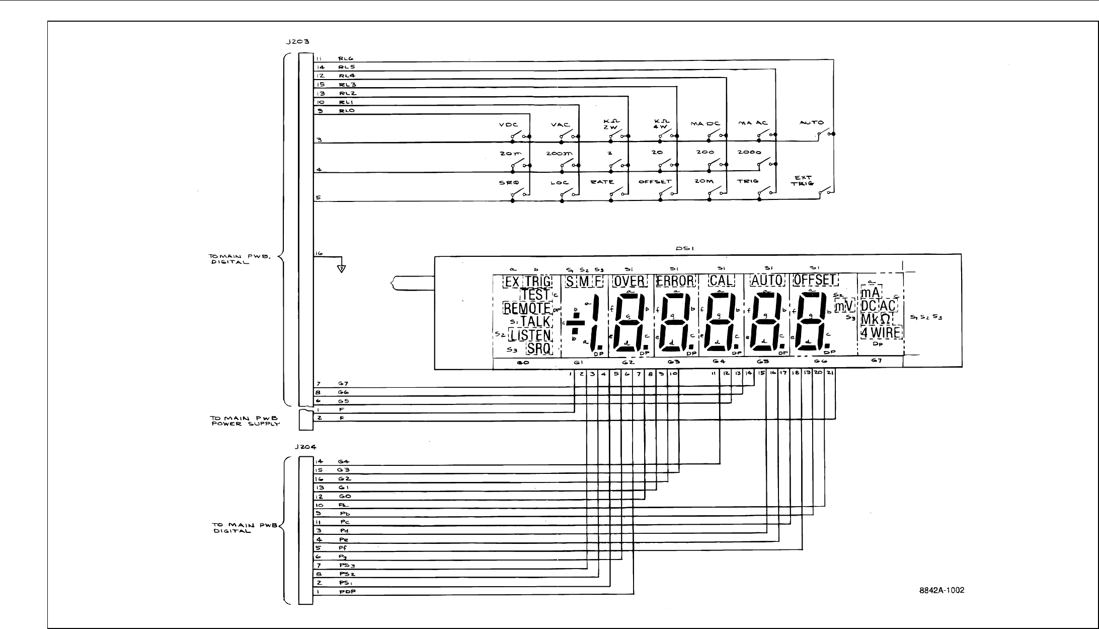
8842A
Instruction Manual
9-14
f9-06_2.wmf
Figure 9-6. Display PCA (cont.)
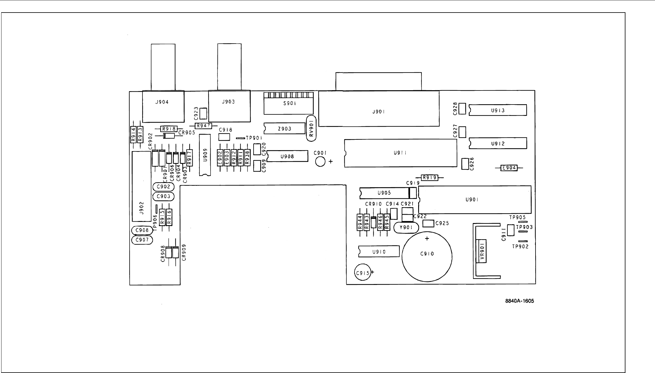
Schematic Diagrams
9
9-15
f9-07_1.wmf
Figure 9-7. IEEE-488 Interface PCA
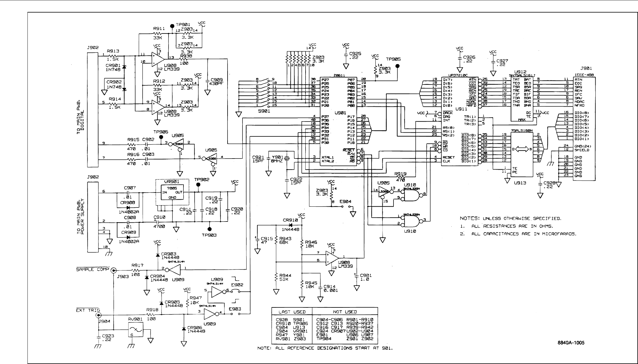
8842A
Instruction Manual
9-16
f9-07_2.wmf
Figure 9-7. IEEE-488 Interface PCA (cont.)
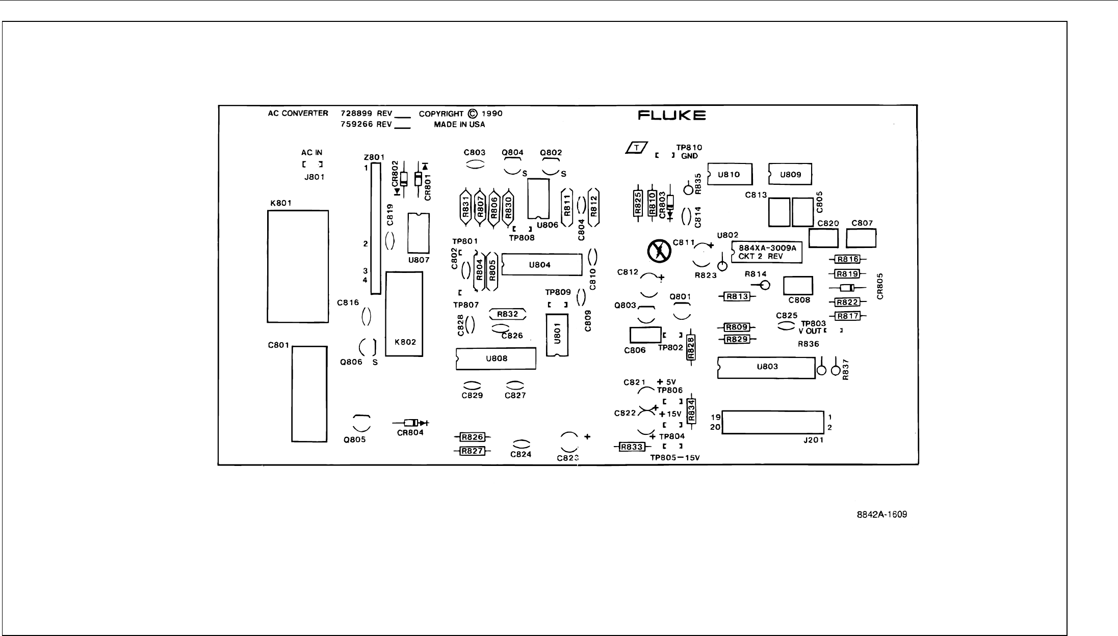
Schematic Diagrams
9
9-17
f9-08_1.wmf
Figure 9-8. IEEE-488 Interface PCA, Option -08
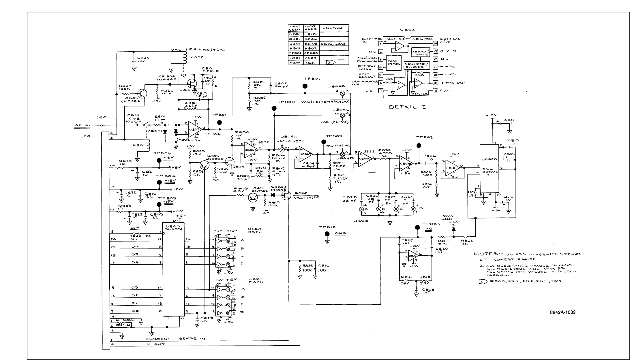
8842A
Instruction Manual
9-18
f9-08_2.wmf
Figure 9-8. IEEE-488 Interface PCA, Option –08 (cont.)
