Fluke Power Supply 5720A Users Manual
5720A to the manual 79d08b52-b679-4929-8297-ad83d22edd9a
2015-02-02
: Fluke Fluke-Fluke-Power-Supply-5720A-Users-Manual-427861 fluke-fluke-power-supply-5720a-users-manual-427861 fluke pdf
Open the PDF directly: View PDF ![]() .
.
Page Count: 570 [warning: Documents this large are best viewed by clicking the View PDF Link!]
- 5700A/5720A Series II Service Manual
- 1. Introduction and Specifications
- Introduction
- Contacting Fluke
- About this Manual
- How to Use this Manual
- Additional Instruction Manuals
- Wideband AC Voltage Module (Option 5700A-03)
- Auxiliary Amplifiers
- Support Equipment and Services
- The Components of the 5700A/5720A Series II Calibrator
- Calibrating the 5700A/5720A Series II Calibrator
- Calibration Check
- Developing a Performance History
- Range Calibration
- DC Zeros Calibration
- Specifications
- DC Voltage Specifications
- AC Voltage Specifications
- Resistance Specifications
- DC Current Specifications
- AC Current Specifications
- Wideband AC Voltage (Option 5700-03) Specifications
- General Specifications
- 2. Theory of Operation
- Introduction
- Calibrator Overview
- Digital Section Overview
- Analog Section Overview
- Functional Description Presented by Output Function
- System Interconnect Detailed Circuit Description
- Digital Section Detailed Circuit Description
- Analog Section Detailed Circuit Description
- Filter/PA Supply (A18), Low-voltage Filter/Regulator Section
- Filter/PA Supply (A18), Power Amplifier Output Supply Section
- Regulator/Guard Crossing Assembly (A17)
- Switch Matrix Assembly (A8)
- Switch Matrix Digital Control
- Switch Matrix Operation: 11V DC and 22V DC Ranges
- Switch Matrix Operation: 2.2V AC and 22V AC Ranges
- Switch Matrix Operation: 220V AC and DC Ranges
- Switch Matrix Operation: 2.2V DC Range
- Calibration of the 2.2V Range
- Switch Matrix Operation: 220 mV DC Range
- Switch Matrix Operation: 220 mV AC Range
- Switch Matrix Operation: 2.2 mV and 22 mV AC Ranges
- Calibration of the mV Ranges
- Internal CAL Zero Amplifier
- Switch Matrix 5725A Amplifier Interface
- DAC Assembly (A11)
- Basic DAC Theory of Operation.
- DAC Assembly Digital Control
- DAC Assembly Reference Circuitry
- Duty-Cycle Control Circuit
- DAC Filter Circuit
- DAC Output Stage
- Sense Current Cancellation Circuit
- Linearity Control Circuit
- Negative Offset Circuit
- DAC Output Switching
- DAC Buffered Reference Sip
- Calibration Hardware
- ADC Amplifier
- ADC Input Selection
- ADC Circuit
- How the DAC is Used in Calibration
- DAC Assembly Calibration
- Oscillator Section Overview
- Oscillator Control Assembly (A12)
- Oscillator Output Assembly (A13)
- Power Amplifier Assembly (A16)
- High Voltage Assemblies (A14 and A15)
- Ohms Overview
- Ohms Main Assembly (A10)
- Ohms Cal Assembly (A9)
- Current/High Resolution Oscillator Assembly Overview (A7)
- Current Input Switching
- Complementary Drive Circuit
- Transconductance Amplifiers
- Shunt Resistors
- Feedback Loop
- Current Output Switching
- Generation of the 2.2A Range
- Current Guard Buffer
- Compliance Limiter
- Current/Compliance Voltage Monitor
- Current Assembly Calibration
- Reference Frequency Amp/Divider
- Phase-Locked Loop
- 5-500k Output Divider
- Hi-Res Output Switching
- Rear Panel Assembly (A21)
- Wideband AC Module (Option -03)
- Wideband Output Attenuators
- Wideband Output RMS Sensor and Amplitude Control Circuit
- Wideband Output Overload Control Circuit
- Wideband Output Digital Control
- Wideband Output Calibration
- 3. Calibration and Verification
- Introduction
- Accessing the Fuse
- Cleaning the Air Filter
- Cleaning the Exterior
- Calibration
- Calibrating the 5700A/5720A Series II to External Standards
- Range Calibration
- Calibrating the Wideband AC Module (Option 5700A-03)
- Performing a Calibration Check
- Full Verification
- Required Equipment for All Tests
- Warm-up Procedure for All Verification Tests
- Resistance Verification Test
- Two-Wire Compensation Verification
- DC Voltage Verification Test
- DC Voltage One-Tenth Scale Linearity Test
- Direct Current Accuracy Verification Test
- AC Voltage Frequency Accuracy Test
- Output Level Tests For AC V Ranges
- AC Current Test( 22 mA to 11A Ranges
- AC Current Test, 2 mA and 200 (A Ranges
- Rationale for Using Metal-Film Resistors to Measure AC Current
- Wideband Frequency Accuracy Test
- Wideband AC Voltage Module Output Verification
- Wideband Output Accuracy at 1 kHz Test
- Wideband Output Flatness Test
- Optional Tests
- Minimum Use Requirements
- Determining Test Limits for Other Calibration Intervals
- Static Awareness
- 4. Maintenance
- Introduction
- Cleaning the Air Filter
- General Cleaning
- Cleaning PCA's
- Access Procedures
- Top and Bottom Covers
- Digital Section Cover
- Analog Section Covers
- Rear Panel Removal and Installation
- Rear Panel Assembly Access
- Front Panel Removal and Installation
- Analog Assembly Removal and Installation
- Digital Assembly Removal and Installation
- Power Transformer Removal and Installation
- Hybrid Cover Removal
- Front/Rear Binding Post Reconfiguration
- Installing a Wideband AC Module (Option -03)
- Clearing Ghost Images from the Control Display
- Replacing the Clock/Calendar Backup Battery
- Using Remote Commands Reserved for Servicing
- 5. Troubleshooting
- Introduction
- Interpreting Diagnostic Fault Codes
- Component-level Troubleshooting
- Troubleshooting the Wideband Output Assembly (A5)
- Troubleshooting the Wideband Oscillator Assembly (A6)
- Troubleshooting the Current/Hi-Res Assembly (A7)
- Troubleshooting the Switch Matrix Assembly (A8)
- Troubleshooting the Ohms Cal Assembly (A9)
- Troubleshooting the Ohms Main Assembly (A10)
- Troubleshooting the DAC Assembly (A11)
- Troubleshooting the Oscillator Control Assembly (A12)
- Troubleshooting the Oscillator Output Assembly (A13)
- Troubleshooting the High Voltage Control Assembly (A14)
- Troubleshooting the High Voltage/High Current Assembly (A15)
- Troubleshooting the Power Amplifier Assembly (A16)
- Troubleshooting the Filter/PA Supply Assembly (A18)
- 6. List of Replaceable Parts
- 7. Schematic Diagrams

®
5700A/5720A Series II
Multi-Function Calibrator
Service Manual
PN 601630
June 1996 Rev. 1, 3/02
©1996, 2002 Fluke Corporation, All rights reserved. Printed in U.S.A.
All product names are trademarks of their respective companies.
LIMITED WARRANTY & LIMITATION OF LIABILITY
Each Fluke product is warranted to be free from defects in material and workmanship
under normal use and service. The warranty period is one year and begins on the date
of shipment. Parts, product repairs and services are warranted for 90 days. This
warranty extends only to the original buyer or end-user customer of a Fluke authorized
reseller, and does not apply to fuses, disposable batteries or to any product which, in
Fluke’s opinion, has been misused, altered, neglected or damaged by accident or
abnormal conditions of operation or handling. Fluke warrants that software will operate
substantially in accordance with its functional specifications for 90 days and that it has
been properly recorded on non-defective media. Fluke does not warrant that software
will be error free or operate without interruption.
Fluke authorized resellers shall extend this warranty on new and unused products to
end-user customers only but have no authority to extend a greater or different warranty
on behalf of Fluke. Warranty support is available if product is purchased through a Fluke
authorized sales outlet or Buyer has paid the applicable international price. Fluke
reserves the right to invoice Buyer for importation costs of repair/replacement parts
when product purchased in one country is submitted for repair in another country.
Fluke’s warranty obligation is limited, at Fluke’s option, to refund of the purchase price,
free of charge repair, or replacement of a defective product which is returned to a Fluke
authorized service center within the warranty period.
To obtain warranty service, contact your nearest Fluke authorized service center or
send the product, with a description of the difficulty, postage and insurance prepaid
(FOB Destination), to the nearest Fluke authorized service center. Fluke assumes no
risk for damage in transit. Following warranty repair, the product will be returned to
Buyer, transportation prepaid (FOB Destination). If Fluke determines that the failure
was caused by misuse, alteration, accident or abnormal condition of operation or
handling, Fluke will provide an estimate of repair costs and obtain authorization before
commencing the work. Following repair, the product will be returned to the Buyer
transportation prepaid and the Buyer will be billed for the repair and return transportation
charges (FOB Shipping Point).
THIS WARRANTY IS BUYER’S SOLE AND EXCLUSIVE REMEDY AND IS IN LIEU OF
ALL OTHER WARRANTIES, EXPRESS OR IMPLIED, INCLUDING BUT NOT LIMITED
TO ANY IMPLIED WARRANTY OF MERCHANTABILITY OR FITNESS FOR A
PARTICULAR PURPOSE. FLUKE SHALL NOT BE LIABLE FOR ANY SPECIAL,
INDIRECT, INCIDENTAL OR CONSEQUENTIAL DAMAGES OR LOSSES,
INCLUDING LOSS OF DATA, WHETHER ARISING FROM BREACH OF WARRANTY
OR BASED ON CONTRACT, TORT, RELIANCE OR ANY OTHER THEORY.
Since some countries or states do not allow limitation of the term of an implied warranty,
or exclusion or limitation of incidental or consequential damages, the limitations and
exclusions of this warranty may not apply to every buyer. If any provision of this
Warranty is held invalid or unenforceable by a court of competent jurisdiction, such
holding will not affect the validity or enforceability of any other provision.
Fluke Corporation Fluke Europe B.V.
P.O. Box 9090 P.O. Box 1186
Everett, WA 98206-9090 5602 BD Eindhoven
U.S.A. The Netherlands
5/94
Interference Information
This equipment generates and uses radio frequency energy and if not installed and used in strict
accordance with the manufacturer’s instructions, may cause interference to radio and television
reception. It has been type tested and found to comply with the limits for a Class B computing
device in accordance with the specifications of Part 15 of FCC Rules, which are designed to
provide reasonable protection against such interference in a residential installation.
Operation is subject to the following two conditions:
• This device may not cause harmful interference.
• This device must accept any interference received, including interference that may cause
undesired operation.
There is no guarantee that interference will not occur in a particular installation. If this equipment
does cause interference to radio or television reception, which can be determined by turning the
equipment off and on, the user is encouraged to try to correct the interference by one of more of
the following measures:
• Reorient the receiving antenna
• Relocate the equipment with respect to the receiver
• Move the equipment away from the receiver
• Plug the equipment into a different outlet so that the computer and receiver are on different
branch circuits
If necessary, the user should consult the dealer or an experienced radio/television technician for
additional suggestions. The user may find the following booklet prepared by the Federal
Communications Commission helpful: How to Identify and Resolve Radio-TV Interference
Problems. This booklet is available from the U.S. Government Printing Office, Washington, D.C.
20402. Stock No. 004-000-00345-4.
Declaration of the Manufacturer or Importer
We hereby certify that the Fluke Model 5700A/5720A Series II Calibrator is in compliance with
BMPT Vfg 243/1991 and is RFI suppressed. The normal operation of some equipment (e.g. signal
generators) may be subject to specific restrictions. Please observe the notices in the users
manual. The marketing and sales of the equipment was reported to the Central Office for
Telecommunication Permits (BZT). The right to retest this equipment to verify compliance with the
regulation was given to the BZT.
Bescheinigung des Herstellers/Importeurs
Hiermit wird bescheinigt, daβ Fluke Models 5700A/5720A Series II Calibrator in Übereinstimung
mit den Bestimmungen der BMPT-AmtsblVfg 243/1991 funk-entstört ist. Der vorschriftsmäßige
Betrieb mancher Geräte (z.B. Meßsender) kann allerdings gewissen Einschränkungen
unterliegen. Beachten Sie deshalb die Hinweise in der Bedienungsanleitung. Dem Bundesamt für
Zulassungen in der Telekcommunikation wurde das Inverkehrbringen dieses Gerätes angezeigt
und die Berechtigung zur Überprüfung der Seire auf Einhaltung der Bestimmungen eingeräumt.
Fluke Corporation

OPERATOR SAFETY
SUMMARY
WARNING
HIGH VOLTAGE
is used in the operation of this equipment
LETHAL VOLTAGE
may be present on the terminals, observe all safety precautions!
To avoid electrical shock hazard, the operator should not electrically
contact the output hi or sense hi binding posts. During operation, lethal
voltages of up to 1100V ac or dc may be present on these terminals.
Whenever the nature of the operation permits, keep one hand away from
equipment to reduce the hazard of current flowing thought vital organs of
the body.
Terms in this Manual
This instrument has been designed and tested in accordance with IEC Publication 348,
Safety Requirements for Electronic Measuring Apparatus. This manual contains information
and warnings which have to be followed by the user to ensure safe operation and to retain
the instrument in safe condition.
Warning statements identify conditions or practices that could result in personal injury or
loss of life.
Caution statements identify conditions or practices that could result in damage to the
equipment or other property.

Symbols Marked on Equipment
DANGER — High Voltage
Protective ground (earth) terminal
Attention — refer to the manual. This symbol indicates that information about
the usage of a feature is contained in the manual.
Power Source
The 5700A/5720A Series II is intended to operate from a power source that will not
apply more than 264V ac rms between the supply conductors or between either supply
conductor and ground. A protective ground connection by way of the grounding
conductor in the power cord is essential for safe operation.
Use the Proper Fuse
To avoid fire hazard, use only the fuse specified on the line voltage selection switch
label, and which is identical in type voltage rating, and current rating.
Grounding the 5700A/5720A Series II
The 5700A/5720A Series II is Safety Class I (grounded enclosure) instruments as
defined in IEC 348. The enclosure is grounded through the grounding conductor of the
power cord. To avoid electrical shock, plug the power cord into a properly wired earth
grounded receptacle before connecting anything to any of the 5700A/5720A Series II
terminals. A protective ground connection by way of the grounding conductor in the
power cord is essential for safe operation.
Use the Proper Power Cord
Use only the power cord and connector appropriate for proper operation of a
5700A/5720A Series II in your country.
Use only a power cord that is in good condition.
Refer cord and connector changes to qualified service personnel.
Do Not Operate in Explosive Atmospheres
To avoid explosion, do not operate the 5700A/5720A Series II in an atmosphere of
explosive gas.
Do Not Remove Cover
To avoid personal injury or death, do not remove the 5700A/5720A Series II cover. Do
not operate the 5700A/5720A Series II without the cover properly installed. There are no
user-serviceable parts inside the 5700A/5720A Series II, so there is no need for the
operator to ever remove the cover.
Do Not Attempt to Operate if Protection May be Impaired
If the 5700A/5720A Series II appears damaged or operates abnormally, protection may
be impaired. Do not attempt to operate it. When in doubt, have the instrument serviced.
SERVICING SAFETY
SUMMARY
FOR QUALIFIED SERVICE
PERSONNEL ONLY
Also refer to the preceding Operator Safety Summary
Do Not Service Alone
Do not perform internal service or adjustment of this product unless another person
capable of rendering first aid and resuscitation is present.
Use Care When Servicing With Power On
Dangerous voltage exist at many points inside this product. To avoid personal injury, do
not touch exposed connections and components while power is on.
Whenever the nature of the operation permits, keep one hand away from equipment to
reduce the hazard of current flowing through vital organs of the body.
Do not wear a grounded wrist strap while working on this product. A grounded wrist strap
increase the risk of current flowing through the body.
Disconnect power before removing protective panels, soldering, or replacing components.
High voltage may still be present even after disconnecting power.

FIRST AID FOR
ELECTRIC SHOCK
Free the Victim From the Live Conductor
Shut off high voltage at once and ground the circuit. If high voltage cannot be turned off
quickly, ground the circuit.
If the circuit cannot be broken or grounded, use a board, dry clothing, or other
nonconductor to free the victim.
Get Help!
Yell for help. Call an emergency number. Request medical assistance.
Never Accept Ordinary and General Tests for Death
Symptoms of electric shock may include unconsciousness, failure to breathe, absence of
pulse, pallor, and stiffness, and severe burns.
Treat the Victim
If the victim is not breathing, begin CPR or mouth-to-mouth resuscitation if you are
certified.
i
Table of Contents
Chapter Title Page
1 Introduction and Specifications........................................................ 1-1
1-1. Introduction .......................................................................................... 1-3
1-2. Contacting Fluke .................................................................................. 1-4
1-3. About this Manual................................................................................ 1-4
1-4. How to Use this Manual....................................................................... 1-4
1-5. Additional Instruction Manuals............................................................ 1-5
1-6. Wideband AC Voltage Module (Option 5700A-03)............................ 1-5
1-7. Auxiliary Amplifiers ............................................................................ 1-6
1-8. 5725A Amplifier.............................................................................. 1-6
1-9. Support Equipment and Services ......................................................... 1-6
1-10. 732B Direct Voltage Reference Standard........................................ 1-7
1-11. 732B-200 Direct Volt Maintenance Program (U.S.A. Only) .......... 1-7
1-12. 742A Series Resistance Standards................................................... 1-7
1-13. Wideband AC Module (Option 5700A-03) Calibration Support .... 1-7
1-14. Service Centers ................................................................................ 1-8
1-15. The Components of the 5700A/5720A Series II Calibrator................. 1-8
1-16. Calibrating the 5700A/5720A Series II Calibrator............................... 1-9
1-17. The Calibration Process................................................................... 1-10
1-18. Establishing Traceability ................................................................. 1-10
1-19. Calibration Reports.......................................................................... 1-11
1-20. Calibration Check................................................................................. 1-11
1-21. Developing a Performance History...................................................... 1-11
1-22. Range Calibration................................................................................. 1-12
1-23. DC Zeros Calibration ........................................................................... 1-12
1-24. Specifications ....................................................................................... 1-12
1-25. Specification Confidence Levels ..................................................... 1-12
1-26. Using Absolute and Relative Uncertainty Specifications................ 1-12
1-27. Using Secondary Performance Specifications................................. 1-13
1-28. DC Voltage Specifications................................................................... 1-14
1-29. AC Voltage Specifications................................................................... 1-17
1-30. Resistance Specifications..................................................................... 1-23
1-31. DC Current Specifications ................................................................... 1-27
1-32. AC Current Specifications ................................................................... 1-30
1-33. Wideband AC Voltage (Option 5700-03) Specifications .................... 1-35

5700A/5720A Series II
Service Manual
ii
1-34. General Specifications.......................................................................... 1-36
1-35. Auxiliary Amplifier Specifications...................................................... 1-37
2 Theory of Operation........................................................................... 2-1
2-1. Introduction .......................................................................................... 2-5
2-2. Calibrator Overview............................................................................. 2-5
2-3. Internal References .......................................................................... 2-5
2-4. Hybrid Reference Amplifiers ...................................................... 2-5
2-5. Fluke Thermal Sensor (FTS)....................................................... 2-5
2-6. Digital-to-Analog Converter (DAC)............................................ 2-6
2-7. Digital Section Overview..................................................................... 2-6
2-8. Analog Section Overview..................................................................... 2-6
2-9. Functional Description Presented by Output Function........................ 2-8
2-10. DC Voltage Functional Description................................................. 2-8
2-11. AC Voltage Functional Description................................................. 2-11
2-12. Wideband AC V Functional Description (Option -03).................... 2-12
2-13. DC Current Functional Description................................................. 2-12
2-14. AC Current Functional Description................................................. 2-12
2-15. Ohms Functional Description .......................................................... 2-13
2-16. System Interconnect Detailed Circuit Description............................... 2-13
2-17. Digital Motherboard Assembly (A4)............................................... 2-13
2-18. Transformer Assembly (A22).......................................................... 2-14
2-19. Analog Motherboard Assembly (A3) .............................................. 2-14
2-20. Front/Rear Binding Posts................................................................. 2-18
2-21. Rear Panel Assembly (A21)............................................................. 2-18
2-22. Filter PA Supply Assembly (A18)................................................... 2-18
2-23. Digital Section Detailed Circuit Description ....................................... 2-18
2-24. Digital Power Supply Assembly (A19)............................................ 2-18
2-25. +5V Power Supply....................................................................... 2-19
2-26. ±12V Power Supplies .................................................................. 2-19
2-27. +35V Power Supply..................................................................... 2-19
2-28. +75V Power Supply..................................................................... 2-20
2-29. +35V and +75V Shut-Down Circuit............................................ 2-20
2-30. CPU (Central Processing Unit) Assembly (A20) ............................ 2-21
2-31. Power-Up and Reset Circuit........................................................ 2-21
2-32. Clock Generation......................................................................... 2-21
2-33. Watchdog Timer.......................................................................... 2-24
2-34. Address Decoding and DTACK (Data Acknowledge)................ 2-24
2-35. Interrupt Controller...................................................................... 2-25
2-36. Glue Logic ................................................................................... 2-25
2-37. RAM (Random-Access Memory)................................................ 2-25
2-38. ROM (Read-Only Memory) ........................................................ 2-25
2-39. Electrically-Erasable Programmable Read-Only Memory
(EEPROM) .................................................................................. 2-26
2-40. DUART (Dual Universal Asynchronous Receiver/transmitter)
Circuit .......................................................................................... 2-26
2-41. Clock/Calendar Circuit................................................................ 2-26
2-42. Clock Filter Circuit...................................................................... 2-27
2-43. CPU to Rear Panel Interface........................................................ 2-27
2-44. CPU to Front Panel Interface....................................................... 2-27
2-45. Fan Monitor ................................................................................. 2-27
2-46. Front Panel Assembly (A2).............................................................. 2-28
2-47. Clock Regeneration Circuitry...................................................... 2-28
2-48. Refresh Failure Detect Circuitry ................................................. 2-28

Contents
(continued)
iii
2-49. Decoding and Timing Circuitry................................................... 2-28
2-50. Control Display Circuitry............................................................ 2-29
2-51. Output Display Circuitry ............................................................. 2-30
2-52. Keyboard Scanner Circuitry........................................................ 2-31
2-53. Knob Encoder Circuitry............................................................... 2-31
2-54. Led Circuitry................................................................................ 2-32
2-55. Keyboard Assembly (A1) ................................................................ 2-32
2-56. Analog Section Detailed Circuit Description....................................... 2-33
2-57. Filter/PA Supply (A18), Low-voltage Filter/Regulator Section...... 2-33
2-58. Unregulated OSC Supplies.......................................................... 2-34
2-59. Unregulated LH Supplies ............................................................ 2-34
2-60. Unregulated S Supplies ............................................................... 2-34
2-61. Triac Circuit................................................................................. 2-34
2-62. FR1 Supplies................................................................................ 2-34
2-63. Unregulated FR1 Supply ............................................................. 2-34
2-64. FR2 Supplies................................................................................ 2-35
2-65. Filter/PA Supply (A18), Power Amplifier Output Supply Section . 2-35
2-66. ±PA Supplies Digital Control...................................................... 2-35
2-67. ±250V and ±500V Supplies ........................................................ 2-37
2-68. +PA and -PA Supplies................................................................. 2-37
2-69. ±PA Supply Current Limit........................................................... 2-37
2-70. Regulator/Guard Crossing Assembly (A17).................................... 2-38
2-71. Voltage Regulator Circuitry ........................................................ 2-38
2-72. Regulated OSC Supplies.............................................................. 2-38
2-73. Regulated LH Supplies................................................................ 2-39
2-74. Regulated S Supplies................................................................... 2-39
2-75. FR1 Supply.................................................................................. 2-40
2-76. FR2 Supply.................................................................................. 2-40
2-77. Guarded Digital Control Circuitry............................................... 2-41
2-87. Switch Matrix Assembly (A8)......................................................... 2-43
2-88. Switch Matrix Digital Control..................................................... 2-44
2-89. Switch Matrix Operation: 11V DC and 22V DC Ranges............ 2-46
2-90. Switch Matrix Operation: 2.2V AC and 22V AC Ranges........... 2-48
2-91. Switch Matrix Operation: 220V AC and DC Ranges.................. 2-48
2-92. Switch Matrix Operation: 2.2V DC Range ................................. 2-51
2-93. Calibration of the 2.2V Range..................................................... 2-53
2-94. Switch Matrix Operation: 220 mV DC Range ............................ 2-53
2-95. Switch Matrix Operation: 220 mV AC Range ............................ 2-56
2-96. Switch Matrix Operation: 2.2 mV and 22 mV AC Ranges......... 2-56
2-97. Calibration of the mV Ranges ..................................................... 2-56
2-98. Internal CAL Zero Amplifier....................................................... 2-59
2-99. Switch Matrix 5725A Amplifier Interface .................................. 2-61
2-100. DAC Assembly (A11)...................................................................... 2-61
2-101. Basic DAC Theory of Operation................................................. 2-61
2-102. DAC Assembly Digital Control................................................... 2-64
2-103. DAC Assembly Reference Circuitry ........................................... 2-64
2-104. Duty-Cycle Control Circuit ......................................................... 2-65
2-105. DAC Filter Circuit....................................................................... 2-66
2-106. DAC Output Stage....................................................................... 2-66
2-107. Sense Current Cancellation Circuit ............................................. 2-67
2-108. Linearity Control Circuit ............................................................. 2-67
2-109. Negative Offset Circuit................................................................ 2-68
2-110. DAC Output Switching................................................................ 2-68
2-111. DAC Buffered Reference Sip...................................................... 2-68
2-112. Calibration Hardware .................................................................. 2-69

5700A/5720A Series II
Service Manual
iv
2-113. ADC Amplifier............................................................................ 2-69
2-114. ADC Input Selection.................................................................... 2-69
2-115. ADC Circuit................................................................................. 2-70
2-116. How the DAC is Used in Calibration .......................................... 2-72
2-117. DAC Assembly Calibration......................................................... 2-72
2-118. Oscillator Section Overview............................................................ 2-73
2-119. Oscillator Control Assembly (A12)................................................. 2-73
2-120. Oscillator Control Digital Control............................................... 2-74
2-121. Oscillator Input Switching........................................................... 2-74
2-122. Sense Current Cancellation ......................................................... 2-74
2-123. Averaging Converter.................................................................... 2-75
2-124. Error Integrator............................................................................ 2-75
2-125. Three-Pole Filter.......................................................................... 2-75
2-126. Analog Amplitude Control Loop................................................. 2-75
2-127. AC/DC Thermal Transfer Circuit................................................ 2-77
2-128. Oscillator Calibration .................................................................. 2-79
2-129. AC/DC Frequency Response Characterization ........................... 2-80
2-130. Oscillator Output Assembly (A13) .................................................. 2-80
2-131. Oscillator Output Digital Control................................................ 2-82
2-132. Quadrature RC Oscillator............................................................ 2-82
2-133. Oscillator Amplitude Control...................................................... 2-83
2-134. Phase−locked Loop...................................................................... 2-83
2-135. 2.2V and 22V Range Output Amplifier....................................... 2-84
2-136. Oscillator Wideband Smd Assembly (A13A1) ........................... 2-84
2-137. Output Stage ................................................................................ 2-85
2-138. Phase Shifter................................................................................ 2-85
2-139. Power Amplifier Assembly (A16) ................................................... 2-85
2-140. Power Amplifier Digital Control Sip Assembly (A16A1) .......... 2-86
2-141. PA Common Circuitry................................................................. 2-87
2-142. +PA and -PA Supplies................................................................. 2-87
2-143. PA Input Stage............................................................................. 2-87
2-144. PA Mid Stage............................................................................... 2-88
2-145. PA Output Stage .......................................................................... 2-88
2-146. PA Sense Current Cancellation Circuitry.................................... 2-89
2-147. PA in Standby.............................................................................. 2-89
2-148. PA Operation: 220V DC Range .................................................. 2-89
2-149. PA Operation: 220V AC Range .................................................. 2-91
2-150. High Voltage Assembly Support Mode....................................... 2-91
2-153. 220V DC Internal Calibration Network ...................................... 2-92
2-154. PA Calibration ............................................................................. 2-92
2-155. High Voltage Assemblies (A14 and A15) ....................................... 2-96
2-156. 1100V AC Range......................................................................... 2-96
2-157. 1100V DC Range......................................................................... 2-98
2-158. HVDC Power Supply Filter Circuit............................................. 2-98
2-159. HV DC Output Series Pass and Current Limit Circuit................ 2-98
2-160. DC HV Amplifier/AC Sense Buffer............................................ 2-100
2-161. 2.2A Range .................................................................................. 2-100
2-162. 2.2A Power Supply Filter Circuit................................................ 2-102
2-163. High Voltage Digital Control ...................................................... 2-103
2-164. High Voltage Calibration............................................................. 2-104
2-165. Calibration of the AC Function ................................................... 2-104
2-166. Calibration of the Current Function. ........................................... 2-106
2-167. High Voltage Magnitude Control................................................ 2-106
2-168. Ohms Overview ............................................................................... 2-108

Contents
(continued)
v
2-169. Ohms Main Assembly (A10) ........................................................... 2-109
2-170. Selection of Resistance Values.................................................... 2-109
2-171. Ohms Main Assembly Support of Current Function Calibration 2-112
2-172. Ohms Digital Control .................................................................. 2-112
2-173. Ohms Cal Assembly (A9)................................................................ 2-112
2-174. Ohms CAL Digital Control ......................................................... 2-112
2-175. 1, 1.9, and Short Resistance......................................................... 2-113
2-176. Two-Wire Ohmmeter Compensation Circuit. ............................. 2-113
2-180. Ohms Calibration......................................................................... 2-115
2-186. Current/High Resolution Oscillator Assembly Overview (A7)....... 2-121
2-187. Current Section............................................................................ 2-122
2-199. High-Resolution Oscillator Section............................................. 2-128
2-204. Rear Panel Assembly (A21)............................................................. 2-130
2-205. Rear Panel Power Supplies.......................................................... 2-131
2-206. Rear Panel Address Mapping ...................................................... 2-131
2-207. Clock Regeneration Circuit ......................................................... 2-132
2-208. IEEE-488 (GPIB) Interface.......................................................... 2-132
2-209. RS-232C Interface ....................................................................... 2-132
2-210. Auxiliary Amplifier Interface...................................................... 2-133
2-211. 5725A Interface ........................................................................... 2-133
2-212. Phase Lock In/Variable Phase out............................................... 2-133
2-213. Rear Panel Relay Control ............................................................ 2-134
2-214. Rear Panel CPU Interface............................................................ 2-134
2-215. Wideband AC Module (Option -03)................................................ 2-135
2-216. Wideband Oscillator Assembly (A6) .......................................... 2-135
2-222. Wideband Output Assembly (A5) ............................................... 2-138
3 Calibration and Verification .............................................................. 3-1
3-1. Introduction .......................................................................................... 3-3
3-2. Accessing the Fuse............................................................................... 3-4
3-3. Cleaning the Air Filter.......................................................................... 3-5
3-4. Cleaning the Exterior ........................................................................... 3-6
3-5. Calibration............................................................................................ 3-6
3-6. Calibrating the 5700A/5720A Series II to External Standards ............ 3-6
3-7. Calibration Requirements ................................................................ 3-7
3-8. When to Adjust the Calibrator’s Uncertainty Specifications .......... 3-7
3-9. Calibration Procedure ...................................................................... 3-8
3-10. Range Calibration................................................................................. 3-14
3-11. Calibrating the Wideband AC Module (Option 5700A-03)................. 3-17
3-12. Performing a Calibration Check........................................................... 3-20
3-13. Full Verification................................................................................... 3-22
3-14. Required Equipment for All Tests................................................... 3-23
3-15. Warm-up Procedure for All Verification Tests ............................... 3-23
3-16. Resistance Verification Test............................................................ 3-25
3-17. Two-Wire Compensation Verification ............................................ 3-27
3-18. DC Voltage Verification Test.......................................................... 3-28
3-19. DC Voltage One-Tenth Scale Linearity Test................................... 3-29
3-20. Direct Current Accuracy Verification Test...................................... 3-30
3-21. AC Voltage Frequency Accuracy Test ............................................ 3-31
3-22. Output Level Tests For AC V Ranges ............................................. 3-31
3-23. AC Current Test, 22 mA to 11A Ranges ......................................... 3-33
3-24. AC Current Test, 2 mA and 200 µA Ranges ................................... 3-36
3-25. Rationale for Using Metal-Film Resistors to Measure AC Current 3-37
3-26. Wideband Frequency Accuracy Test............................................... 3-38

5700A/5720A Series II
Service Manual
vi
3-27. Wideband AC Voltage Module Output Verification....................... 3-38
3-28. Wideband Output Accuracy at 1 kHz Test........................................... 3-39
3-29. Wideband Output Flatness Test ........................................................... 3-40
3-30. Wideband Flatness Calibration Procedure....................................... 3-41
3-31. Optional Tests ...................................................................................... 3-42
3-32. DC Voltage Load Regulation Test................................................... 3-42
3-33. DC Voltage Linearity Test............................................................... 3-43
3-34. DC Voltage Output Noise (10 Hz to 10 kHz) Test.......................... 3-43
3-35. DC Voltage Output Noise (0.1 to 10 Hz) Test................................. 3-45
3-36. AC Voltage Distortion Test ............................................................. 3-45
3-37. Wideband Distortion Testing........................................................... 3-45
3-38. AC Voltage Overshoot Test............................................................. 3-46
3-39. Minimum Use Requirements................................................................ 3-46
3-40. Determining Test Limits for Other Calibration Intervals..................... 3-48
4 Maintenance....................................................................................... 4-1
4-1. Introduction .......................................................................................... 4-3
4-2. Cleaning the Air Filter.......................................................................... 4-3
4-3. General Cleaning.................................................................................. 4-4
4-4. Cleaning PCA’s..................................................................................... 4-4
4-5. Access Procedures................................................................................ 4-4
4-6. Top and Bottom Covers................................................................... 4-4
4-7. Digital Section Cover....................................................................... 4-4
4-8. Analog Section Covers..................................................................... 4-4
4-9. Rear Panel Removal and Installation............................................... 4-4
4-10. Rear Panel Assembly Access........................................................... 4-5
4-11. Front Panel Removal and Installation.............................................. 4-6
4-12. Display Assembly Removal and Installation............................... 4-6
4-13. Keyboard Assembly Removal and Installation ........................... 4-7
4-14. Analog Assembly Removal and Installation.................................... 4-7
4-15. Digital Assembly Removal and Installation .................................... 4-9
4-16. Power Transformer Removal and Installation ................................. 4-9
4-17. Hybrid Cover Removal .................................................................... 4-9
4-18. Front/Rear Binding Post Reconfiguration............................................ 4-9
4-19. Installing a Wideband AC Module (Option -03).................................. 4-11
4-20. Clearing Ghost Images from the Control Display................................ 4-11
4-21. Replacing the Clock/Calendar Backup Battery.................................... 4-11
4-22. Using Remote Commands Reserved for Servicing.............................. 4-12
4-23. Using the ETIME Command............................................................ 4-12
5 Troubleshooting................................................................................. 5-1
5-1. Introduction .......................................................................................... 5-3
5-2. Interpreting Diagnostic Fault Codes..................................................... 5-3
5-3. Component-level Troubleshooting....................................................... 5-40
5-4. Troubleshooting the Wideband Output Assembly (A5) .................. 5-40
5-5. Troubleshooting the Wideband Oscillator Assembly (A6) ............. 5-42
5-6. Troubleshooting the Current/Hi-Res Assembly (A7)...................... 5-47
5-7. Current Section............................................................................ 5-47
5-8. Hi-Res Oscillator Section............................................................ 5-52
5-9. Troubleshooting the Switch Matrix Assembly (A8)........................ 5-54
5-10. Troubleshooting the Ohms Cal Assembly (A9)............................... 5-56
5-11. Two-wire Compensation Circuit ................................................. 5-56
5-12. Troubleshooting the Ohms Main Assembly (A10).......................... 5-57

Contents
(continued)
vii
5-13. Troubleshooting the DAC Assembly (A11) .................................... 5-58
5-14. Duty-cycle Control Circuit .......................................................... 5-63
5-15. ADC Circuit................................................................................. 5-67
5-16. Buffered Reference SIP Assembly (A11A2):.............................. 5-68
5-17. Troubleshooting the Oscillator Control Assembly (A12)................ 5-69
5-18. Troubleshooting the Oscillator Output Assembly (A13)................. 5-72
5-19. Troubleshooting the High Voltage Control Assembly (A14).......... 5-74
5-20. Magnitude Control Circuit........................................................... 5-76
5-21. Troubleshooting the High Voltage/High Current Assembly (A15). 5-77
5-22. Troubleshooting the Power Amplifier Assembly (A16).................. 5-79
5-23. Troubleshooting the Filter/PA Supply Assembly (A18) ................. 5-82
6 List of Replaceable Parts .................................................................. 6-1
6-1. Introduction .......................................................................................... 6-3
6-2. How to Obtain Parts ............................................................................. 6-3
6-3. Manual Status Information................................................................... 6-3
6-4. Newer Instruments................................................................................ 6-3
6-5. Service Centers..................................................................................... 6-4
7 Schematic Diagrams.......................................................................... 7-1

5700A/5720A Series II
Service Manual
viii
ix
List of Tables
Table Title Page
1-1. Auxiliary Amplifier Data....................................................................................... 1-6
1-2. 5720A Series II DC Voltage Specifications: 99 % and 95 % Confidence Levels 1-14
1-3. 5700A Series II DC Voltage Specifications: 99 % and 95 % Confidence Levels 1-15
1-4. DC Voltage Secondary Performance Specifications and Operating
Characteristics ....................................................................................................... 1-16
1-5. 5720A Series II AC Voltage Specifications: 99 % Confidence Level.................. 1-17
1-6. 5720A Series II AC Voltage Specifications: 95 % Confidence Level.................. 1-18
1-7. 5700A Series II AC Voltage Specifications: 99 % Confidence Level.................. 1-19
1-8. 5700A Series II AC Voltage Specifications: 95 % Confidence Level.................. 1-20
1-9. AC Voltage Secondary Performance Specifications and Operating
Characteristics ....................................................................................................... 1-21
1-10. 5720A Series II Resistance Specifications: 99 % and 95 % Confidence Levels .. 1-23
1-11. 5700A Series II Resistance Specifications: 99 % and 95 % Confidence Levels .. 1-24
1-12. Resistance Secondary Performance Specifications and Operating
Characteristics ....................................................................................................... 1-25
1-13. Current Derating Factors ....................................................................................... 1-26
1-14. 5720A Series II DC Current Specifications: 99 % and 95 % Confidence Levels. 1-27
1-15. 5700A Series II DC Current Specifications: 99 % and 95 % Confidence Levels. 1-28
1-16. DC Current Secondary Performance Specifications and Operating
Characteristics ....................................................................................................... 1-29
1-17. 5720A Series II AC Current Specifications: 99 % Confidence Level .................. 1-30
1-18. 5720A Series II AC Current Specifications: 95 % Confidence Level .................. 1-31
1-19. 5700A Series II AC Current Specifications: 99 % Confidence Level .................. 1-32
1-20. 5700A Series II AC Current Specifications: 95 % Confidence Level .................. 1-33
1-21. AC Current Secondary Performance Specifications and Operating
Characteristics ....................................................................................................... 1-34
1-22. Wideband AC Voltage (Option 5700-03) Specifications...................................... 1-35
2-1. Analog Motherboard Connectors .......................................................................... 2-17
2-2. Supplies Generated by the Digital Power Supply ................................................. 2-19
2-3. CPU Acronym Glossary ........................................................................................ 2-23
2-4. CPU Memory Map ................................................................................................ 2-24
2-5. CPU Interrupts, Priorities, and Vectors................................................................. 2-25

5700A/5720A Series II
Service Manual
x
2-6. Front Panel Memory Map...................................................................................... 2-29
2-7. Control Lines for the Keyboard LEDs................................................................... 2-32
2-8. Unregulated Supplies from the Filter Assembly ................................................... 2-33
2-9. Regulated Supplies from the Filter/PA Supply ..................................................... 2-33
2-10. Regulated Outputs from the Regulator/Guard Crossing Assembly ...................... 2-39
2-11. Inguard CPU Memory Map................................................................................... 2-41
2-12. Inguard CPU Interrupts.......................................................................................... 2-43
2-13. PA and -PA Supply Settings at Different Outputs ................................................ 2-87
2-14. AC and DC Current Ranges................................................................................... 2-122
2-15. Relay Settings for Current Range Selection.......................................................... 2-125
2-16. Divider Settings and VCO Frequencies................................................................. 2-131
3-1. Standards for Calibrating 5700A/5720A Series II ................................................ 3-7
3-2. List of Required Equipment for Main Output ....................................................... 3-24
3-3. Equipment Required for Resistance Testing ......................................................... 3-25
3-4. Low Value Resistance Calibration Using a Current Source.................................. 3-27
3-5. Equipment Required for DC Voltage Testing ....................................................... 3-28
3-6. Equipment Required for Direct Current Test ........................................................ 3-30
3-7. Equipment Required for AC V Output Level Tests .............................................. 3-31
3-8. 5790A Adjustment Counts .................................................................................... 3-33
3-9. Equipment Required for 22 mA to 11A Alternating Current Test Using
the 5790A Input 1 .................................................................................................. 3-33
3-10. Equipment Required for Alternating Current Accuracy Test for the 2 mA
and 200 uA Ranges................................................................................................ 3-36
3-11. Equipment Required for Testing and Calibrating the Wideband Option.............. 3-39
3-12. Wideband Adjustment Tolerance .......................................................................... 3-40
3-13. Equipment Required For DC V Optional Tests..................................................... 3-42
3-14. Equipment Required for Distortion Test ............................................................... 3-45
3-15. Minimum Use Requirements................................................................................. 3-47
3-16. 5720A Resistance Test Record.............................................................................. 3-50
3-17. 5700A Resistance Test Record.............................................................................. 3-52
3-18. DC Voltage Test Record for 5720A ...................................................................... 3-54
3-19. DC Voltage Test Record for 5700A ...................................................................... 3-55
3-20. Direct Current Accuracy Test Record (5720A)..................................................... 3-56
3-21. Direct Current Accuracy Test Record (5700A)..................................................... 3-57
3-22. AC Voltage Frequency Accuracy Test Record ..................................................... 3-57
3-23. 5720A AC Voltage Output Test Record................................................................ 3-58
3-24. 5700A AC Voltage Output Test Record................................................................ 3-60
3-25. AC Voltage 2 mV Range Test Record .................................................................. 3-61
3-26. 5720A AC Current 20 mA to 10A Accuracy Test Record.................................... 3-62
3-27. 5700A AC Current 20 mA to 10A Accuracy Test Record.................................... 3-63
3-28. 5720A AC Current 2 mA and 200 mA Accuracy Test Record ............................. 3-64
3-29. 5700A AC Current 2 mA and 200µA Accuracy Test Record............................... 3-64
3-30. Wideband Frequency Accuracy Testi Record....................................................... 3-65
3-31. Wideband Accuracy at 1 kHz Test Record............................................................ 3-66
3-32. Wideband Flatness Test Record ............................................................................ 3-66
3-33. Wideband Absolute Error 10 Hz to 500 kHz......................................................... 3-68
3-34. Load Regulation Test Record................................................................................ 3-69
3-35. DC Voltage Linearity Test Record....................................................................... 3-69
3-36. DC Voltage Output Noise Test.............................................................................. 3-69
3-37. AC V Distortion Test Summary ............................................................................ 3-70

Contents
(continued)
xi
3-38. Test Record for Flatness Check of the AC 2 mV Range....................................... 3-70
5-1. Verifying Multiplexer U 6..................................................................................... 5-46
5-2. Ohms Main Resistance Tolerance ......................................................................... 5-58
6-1. Front Panel Final Assembly .................................................................................. 6-5
6-2. A1 Keyboard PCA................................................................................................. 6-12
6-3. A2 Front Panel PCA .............................................................................................. 6-14
6-4. A3 Analog Motherboard PCA............................................................................... 6-17
6-5. A4 Digital Motherboard PCA................................................................................ 6-19
6-6. A5 Wideband Output PCA, Option -03................................................................ 6-21
6-7. A6 Wideband Ocillator PCA, Option -03.............................................................. 6-25
6-8. A7 Current/High-Res Oscillator PCA................................................................... 6-29
6-9. A8 Switch Matrix PCA.......................................................................................... 6-33
6-10. A9 Ohms Cal PCA................................................................................................. 6-36
6-11. A10 Ohms Main PCA............................................................................................ 6-39
6-12. A11 DAC PCA ...................................................................................................... 6-41
6-13. A11A1 DAC Filter SIP PCA................................................................................. 6-46
6-14. A11A2 DAC Buffered Reference SIP PCA .......................................................... 6-48
6-15. A12 Oscillator Control PCA.................................................................................. 6-50
6-16. A13 Oscillator Output PCA................................................................................... 6-54
6-17. A13A1 Oscillator Wideband SMD PCA.............................................................. 6-58
6-18. A14 High Voltage Control PCA............................................................................ 6-60
6-19. A15 High Voltage/High Current PCA................................................................... 6-63
6-20. A16 Power Amplifier PCA.................................................................................... 6-66
6-21. A16A1 Power Amplifier Digital Control SIP PCA............................................... 6-70
6-22. A17 Regulator/Guard Crossing PCA..................................................................... 6-72
6-23. A18 Filter/PA Supply PCA ................................................................................... 6-75
6-24. A19 Digital Power Supply PCA............................................................................ 6-79
6-25. A20 CPU PCA....................................................................................................... 6-82
6-26. A20 CPU PCA....................................................................................................... 6-83
6-27. A21 Rear Panel PCA ............................................................................................. 6-85

5700A/5720A Series II
Service Manual
xii
xiii
List of Figures
Figure Title Page
1-1. Time and Costs: Calibrator Calibration................................................................. 1-10
1-2. Volt-Hertz Capability ............................................................................................ 1-22
2-1. Digital Section Block Diagram.............................................................................. 2-7
2-2. Analog Section Block Diagram, Part .................................................................... 2-9
2-3. Analog Section Block Diagram, Part .................................................................... 2-10
2-4. System Interconnections........................................................................................ 2-15
2-5. CPU Assembly Block Diagram............................................................................. 2-22
2-6. Power Amplifier Output Supply Simplified Schematic ........................................ 2-36
2-7. Switch Matrix Assembly Simplified Schematic.................................................... 2-45
2-8. Switch Matrix Configuration for 11V DC and 22V DC Ranges........................... 2-47
2-9. Switch Matrix Configuration for 2.2V and 22V AC Ranges ................................ 2-50
2-10. Switch Matrix Configuration for 220V DC and AC Ranges................................. 2-50
2-11. Switch Matrix Configuration for 2.2V DC Range ................................................ 2-52
2-12. Calibration of the 2.2V DC Range ........................................................................ 2-54
2-13. Switch Matrix Configuration for 220 mV DC Range ........................................... 2-56
2-14. V AC, 2.2 mV AC, and 22 mV AC Range............................................................ 2-57
2-15. Divider Calibration................................................................................................ 2-58
2-16. Divider Gain Calibration ....................................................................................... 2-60
2-17. DAC Assembly Simplified Schematic .................................................................. 2-63
2-18. ADC Circuit Measurement Functions................................................................... 2-71
2-19. Oscillator Control Analog Control Loop............................................................... 2-76
2-20. AC/DC Thermal Transfer Circuit.......................................................................... 2-78
2-21. Quadrature RC Oscillator Circuit.......................................................................... 2-81
2-22. Power Amplifier Simplified Schematic................................................................. 2-90
2-23. Power Amplifier DC Calibration Network............................................................ 2-93
2-24. Power Amplifier Calibration AC Attenuator......................................................... 2-95
2-25. High Voltage/High Current Assembly 1100V AC Range..................................... 2-97
2-26. High Voltage/High Current Assembly 1100V DC Range..................................... 2-99
2-27. High Voltage/High Current Assembly 2.2A AC and DC Ranges......................... 2-102
2-28. High Voltage/High Current Assembly Calibration............................................... 2-106
2-29. High Voltage/High Current Assembly 2.2A Range Calibration........................... 2-107
2-30. Ohms Assemblies Simplified Schematic............................................................... 2-111

5700A/5720A Series II
Service Manual
xiv
2-31. Ohms Main Assembly Simplified Schematic........................................................ 2-111
2-32. Two-Wire Lead Drop Compensatin Circuit .......................................................... 2-114
2-33. Calibration to an External 10 kΩ Standard ........................................................... 2-116
2-34. Ratio Calibration, 10Ω From 100Ω....................................................................... 2-120
2-35. Current Output Simplified Schematic ................................................................... 2-123
2-36. Current Assembly Calibration............................................................................... 2-128
2-37. Wideband Output Assembly Simplified Schematic.............................................. 2-139
3-1. Accessing the Fuse ................................................................................................ 3-4
3-2. Accessing the Air Filter......................................................................................... 3-5
3-3. 732B External Calibration Connections................................................................ 3-9
3-4. 742A-1 and 742A-10k External Calibration Connections .................................... 3-12
3-5. 220V DC Range Calibration Connections............................................................. 3-17
3-6. Wideband Module Calibration Connection........................................................... 3-19
3-7. Overview of Verification Tests ............................................................................. 3-22
3-8. 1 Ohm and 10 Ohm Resistor Verification............................................................. 3-26
3-9. Direct Current Accuracy Test Setup...................................................................... 3-30
3-10. 1 MHz Low Pass Filter.......................................................................................... 3-31
3-11. AC Voltage Test Setup .......................................................................................... 3-32
3-12. Alternating Current Test Setup.............................................................................. 3-35
3-13. Alternating Current Test Setup2 mA and 200 µA................................................. 3-36
3-14. Metal Film Resistor Equivalent Circuit................................................................. 3-37
3-15. Metal Film Resistor in Test Circuit....................................................................... 3-37
3-16. Wideband Accuracy at 1 kHz Test Setup.............................................................. 3-39
3-17. Wideband Flatness Test Setup............................................................................... 3-40
3-18. DC Voltage Linearity Test..................................................................................... 3-43
3-19. DC Voltage Output Noise Test Setup.................................................................... 3-44
3-20. Determining Other Test Limits.............................................................................. 3-49
4-1. Air Filter ................................................................................................................ 4-3
4-2. Rear Panel Removal .............................................................................................. 4-5
4-3. Rear Panel Assembly Access................................................................................. 4-5
4-4. Front Panel Removal ............................................................................................. 4-6
4-5. Analog and Digital Assemblies ............................................................................. 4-8
5-1. Waveform at TP10................................................................................................. 5-42
5-2. Waveform at TP1................................................................................................... 5-43
5-3. Waveform at TP15................................................................................................. 5-44
5-4. Waveform at Pins 14 and 15 of U1 ....................................................................... 5-45
5-5. Waveform at Pin 6 of U9....................................................................................... 5-46
5-6. Waveform at Pin 11 of K2..................................................................................... 5-48
5-7. Waveform at Pin 6 of K2....................................................................................... 5-49
5-8. Verifying the 220 uA Range of the 220 µA/2.2 mA Amp Circuit ........................ 5-49
5-9. Verifying the 2.2 mA Range of the 220 µA/2.2 mA Amp Circuit........................ 5-50
5-10. Verifying the 22 mA Range of the 22 mA/220 mA Amp Circuit......................... 5-50
5-11. Verifying the 220 mA Range of the 22 mA/220 mA Amp Circuit....................... 5-51
5-12. Waveform at Pin 4 of U13..................................................................................... 5-52
5-13. Waveform at TP12................................................................................................. 5-53
5-14. Waveform at TP13................................................................................................. 5-54
5-15. Waveform at TP16................................................................................................. 5-55
5-16. Waveform at Pin 13 of U6..................................................................................... 5-57
5-17. Waveform at TP6................................................................................................... 5-59

Contents
(continued)
xv
5-18. Waveform at TP4, Calibrator Set to 0V ................................................................ 5-59
5-19. Waveform at TP4, Calibrator Set to 6.5V ............................................................. 5-60
5-20. Waveform at TP7................................................................................................... 5-61
5-21. Waveform at TP5................................................................................................... 5-62
5-22. Waveform at Pin 10 of U6..................................................................................... 5-64
5-23. Waveform at Pin 6 of U13..................................................................................... 5-65
5-24. Waveform at Pin 4 of U10..................................................................................... 5-65
5-25. Waveform at TP6................................................................................................... 5-66
5-26. Waveform at Pin 7 of U12..................................................................................... 5-67
5-27. Waveform at Anode of CR4.................................................................................. 5-70
5-28. Waveform at Pin 6 of U11..................................................................................... 5-70
5-29. DC Sense Buffer Waveform TP6 .......................................................................... 5-71
5-30. AC Sense Buffer Waveform at TP6 ...................................................................... 5-72
5-31. Waveform at TP 3.................................................................................................. 5-75
5-32. Waveform at Pin 18 of Hybrid H4 ........................................................................ 5-79
5-33. Power Amplifier with Calibrator Set to 22V at 1 kHz .......................................... 5-80
6-1. Front Panel Final Assembly .................................................................................. 6-6
6-2. Chassis Final Assembly......................................................................................... 6-8
6-3. Rear Panel Final Assembly................................................................................... 6-11
6-4. A1 Keyboard PCA................................................................................................. 6-13
6-5. A2 Front Panel PCA .............................................................................................. 6-16
6-6. A3 Analog Motherboard PCA............................................................................... 6-18
6-7. A4 Digital Motherboard PCA................................................................................ 6-20
6-8. A5 Wideband Output PCA, Option -03................................................................. 6-24
6-9. A6 Wideband Oscillator PCA, Option -03............................................................ 6-28
6-10. A7 Current/HIgh-Res Oscillator PCA................................................................... 6-32
6-11. A8 Switch Matrix PCA.......................................................................................... 6-35
6-12. A9 Ohms Cal PCA................................................................................................. 6-38
6-13. A10 Ohms Main PCA............................................................................................ 6-40
6-14. A11 DAC PCA ...................................................................................................... 6-45
6-15. A11A1 DAC Filter SIP PCA................................................................................. 6-47
6-16. A11A2 DAC Buffered Reference SIP PCA .......................................................... 6-49
6-17. A12 Oscillator Control PCA.................................................................................. 6-53
6-18. A13 Oscillator Output PCA................................................................................... 6-57
6-19. A13A1 Oscillator Wideband SMD PCA.............................................................. 6-59
6-20. A14 High Voltage Control PCA............................................................................ 6-62
6-21. A15 High Voltage/High Current PCA................................................................... 6-65
6-22. A16 Power Amplifier PCA.................................................................................... 6-69
6-23. A16A1 Power Amplifier Digital Control SIP PCA............................................... 6-71
6-24. A17 Regulator/Guard Crossing PCA..................................................................... 6-74
6-25. A18 Filter/PA Supply PCA ................................................................................... 6-78
6-26. A19 Digital Power Supply PCA............................................................................ 6-81
6-27. A20 CPU PCA....................................................................................................... 6-84
6-28. A21 Rear Panel PCA ............................................................................................. 6-87

5700A/5720A Series II
Service Manual
xvi
1-1
Chapter 1
Introduction and Specifications
Title Page
1-1. Introduction .......................................................................................... 1-3
1-2. Contacting Fluke .................................................................................. 1-4
1-3. About this Manual................................................................................ 1-4
1-4. How to Use this Manual....................................................................... 1-4
1-5. Additional Instruction Manuals............................................................ 1-5
1-6. Wideband AC Voltage Module (Option 5700A-03)............................ 1-5
1-7. Auxiliary Amplifiers ............................................................................ 1-6
1-8. 5725A Amplifier.............................................................................. 1-6
1-9. Support Equipment and Services ......................................................... 1-6
1-10. 732B Direct Voltage Reference Standard........................................ 1-7
1-11. 732B-200 Direct Volt Maintenance Program (U.S.A. Only) .......... 1-7
1-12. 742A Series Resistance Standards................................................... 1-7
1-13. Wideband AC Module (Option 5700A-03) Calibration Support .... 1-7
1-14. Service Centers ................................................................................ 1-8
1-15. The Components of the 5700A/5720A Series II Calibrator................. 1-8
1-16. Calibrating the 5700A/5720A Series II Calibrator............................... 1-9
1-17. The Calibration Process................................................................... 1-10
1-18. Establishing Traceability ................................................................. 1-10
1-19. Calibration Reports.......................................................................... 1-11
1-20. Calibration Check................................................................................. 1-11
1-21. Developing a Performance History...................................................... 1-11
1-22. Range Calibration................................................................................. 1-12
1-23. DC Zeros Calibration ........................................................................... 1-12
1-24. Specifications ....................................................................................... 1-12
1-25. Specification Confidence Levels ..................................................... 1-12
1-26. Using Absolute and Relative Uncertainty Specifications................ 1-12
1-27. Using Secondary Performance Specifications................................. 1-13
1-28. DC Voltage Specifications................................................................... 1-14
1-29. AC Voltage Specifications................................................................... 1-17

5700A/5720A Series II Calibrator
Service Manual
1-2
1-30. Resistance Specifications..................................................................... 1-23
1-31. DC Current Specifications ................................................................... 1-27
1-32. AC Current Specifications ................................................................... 1-30
1-33. Wideband AC Voltage (Option 5700-03) Specifications .................... 1-35
1-34. General Specifications.......................................................................... 1-36
1-35. Auxiliary Amplifier Specifications...................................................... 1-37

Introduction and Specifications
Introduction
1
1-3
1-1. Introduction
The Fluke Model 5700A/5720A Series II calibrators are precise instruments that
calibrate a wide variety of electrical measuring instruments. These calibrators maintain
high accuracy over a wide ambient temperature range, allowing them to test instruments
in any environment, eliminating the restrictions to calibrate only in a temperature-
controlled standards laboratory. With a 5700A/5720A Series II, you can calibrate
precision multimeters that measure ac or dc voltage, ac or dc current, and resistance. The
5720A Series II operates in a similar manner to the 5700A Series II, the difference is that
the 5720A Series II has a considerably higher specified accuracy. Option 5700A-03
Wideband AC Voltage, which is available for both the 5700A Series II and the 5720A
Series II, extends this workload to include rf voltmeters.
Specifications are provided at the end of this chapter. The calibrator is a fully-
programmable precision source of the following:
• DC voltage to 1100V
• AC voltage to 1100V, with output available from 10 Hz to 1.2 MHz.
• AC and DC current to 2.2A, with output available from 10 Hz to 10 kHz
• Resistance in values of 1x10n and 1.9x10n from 1Ω to 100 MΩ, plus a short.
• Optional wideband ac voltage from 300 µV to 3.5V into 50Ω (-57 dBm to
+24 dBm), 10 Hz to 30 MHz.
Features of the calibrator include the following:
• Internal environmentally-controlled references allowing the calibrator to maintain
full performance over a wide ambient temperature range.
• Automatic meter error calculation obtained through using a simple output adjust
knob; the display shows linearity, offset, and scale errors.
• Keys that multiply and divide the output value by 10 to simplify work on meters
with calibration points at decade multiples of a fraction of full-scale.
• Programmable entry limits used for restricting the levels that can be keyed into the
calibrator, preventing access to levels that may be harmful to equipment or
personnel.
• A s key that provides the capability of displaying the instrument’s specification at
the selected operating point, calibration interval, and specification confidence level.
• An auxiliary current binding post that allows you to calibrate meters with separate
current inputs without moving cables.
• Real-time clock and calendar for date stamping reports.
• Offset and scaling modes that simplify linearity testing of multimeters.
• Variable phase reference signal output and phase-lock input.
• Interface for the Fluke 5725 Amplifier.
• Standard IEEE-488 (GPIB) interface, complying with ANSI/IEEE Standards 488.1-
1987 and 488.2-1987.
• Selectable normal remote mode or emulation of the Fluke 5100B and 5200A Series
calibrators in functions and response to system controller software
• EIA Standard RS-232C serial data interface for printing, displaying, or transferring
internally-stored calibration constants, and for remote control of the calibrator.

5700A/5720A Series II Calibrator
Service Manual
1-4
• Extensive internal self testing and diagnostics of analog and digital functions.
• A traceable calibration procedure for all modes and ranges that requires only 10V,
1Ω, and 10 kΩ external standards, with only occasional independent verification.
• Fast, simple, automated calibration check providing added confidence between
calibration recalls, and data that can be used to document and characterize the
calibrator’s performance between calibration recalls.
1-2. Contacting Fluke
To order accessories, receive operating assistance, or get the location of the nearest
Fluke distributor or Service Center, call:
USA: 1-888-99-FLUKE (1-888-993-5853)
Canada: 1-800-36-FLUKE (1-800-363-5853)
Europe: +31 402-678-200
Japan: +81-3-3434-0181
Singapore: +65-738-5655
Anywhere in the world: +1-425-446-5500
Or, visit Fluke's Web site at www.fluke.com.
1-3. About this Manual
This manual provides complete information for installing the calibrator and operating it
from the front panel keys and in remote. It also provides a glossary of calibration-related
terms as well as general items such as specifications and error code information. The
following topics are covered in this manual:
• Installation
• Operating controls and features
• Front panel operation
• Remote operation (IEEE-488 bus or serial port remote control)
• Serial port operation (printing, displaying, or transferring data, and setting up for
serial port remote control)
• Operator maintenance, including how to calibrate the 5700A/5720A Series II
• Options and accessories
1-4. How to Use this Manual
Use the following list to find the location of specific information.
• Quick setup procedure: 5700A/5720A Series II Operators Reference Guide
• Unpacking and setup: Chapter 2.
• Installation and rack mounting: Chapter 2; also the rack mount kit instruction sheet
• AC line power and interface cabling: Chapter 2
• Controls, indicators, and displays: Chapter 3
• Front panel operation: Chapter 4
• Cabling to a UUT (Unit Under Test): Chapter 4

Introduction and Specifications
Additional Instruction Manuals
1
1-5
• Using auxiliary amplifiers: Chapter 4
• Self calibration: Chapters 1 and 7
• Remote operation (IEEE-488 or serial): Chapter 5
• Options and accessories: Chapters 2 and 8
• Instrument specifications: The end of this Chapter
• Theory of operation: Chapter 2 of the 5700A/5720A Series II Service Manual
1-5. Additional Instruction Manuals
The 5700A/5720A Series II Calibrators ship with a complete manual set that contains
information for the operator and service or maintenance technicians. The set includes:
• 5700A/5720A Series II Getting Started Manual (PN 1668111)
• 5700A/5720A Series II Operator Reference Guide (PN 601648)
• 5700A/5720A Series II Remote Programming Reference Guide (PN 601655)
• 5700A/5720A Series II Operator Manual (provided on CD-ROM, PN 1668127, or a
printed copy is available for purchase through the Fluke Service Department under
PN 601622)
• 5700A/5720A Series II Service Manual (provided on CD-ROM, PN 1668127, or a
printed copy is available for purchase through the Fluke Service Department under
PN 105798)
Order additional copies of these instruction manuals separately using the part numbers
provided. For ordering instructions, refer to the Fluke Catalog or contact a Fluke sales
representative.
1-6. Wideband AC Voltage Module (Option 5700A-03)
The Wideband AC Voltage Module (Option 5700A-03) can be installed in both the
5700A and 5720A Series II Calibrators. The module is a high-accuracy, low-noise,
extremely flat ac voltage source for calibrating rf voltmeters, with a frequency range of
10 Hz to 30 MHz. Output is in seven ranges from 300 µV (-57 dBm) to 3.5 V (+24 dBm)
through a Type-N coaxial connector into a 50 Ω load. The output level is selected in
volts or dBm through either the front panel controls or under remote control.
The wideband module also functions with the calibrator’s output adjust controls that let
display the error of a wideband meter in either percentage of output or in decibels.
Included with the wideband module is a Type-N output cable and a 50 Ω terminator. The
wideband module is calibrated to the end of its standard-equipment output cable.

5700A/5720A Series II Calibrator
Service Manual
1-6
1-7. Auxiliary Amplifiers
The Fluke Model 5725A Amplifier is available to extend the high voltage performance
and current range of the calibrator:
Interface connectors on the calibrator’s rear panel accept cables to directly operate a
5725A. Three amplifiers can be connected to the calibrator at the same time, but only
one output can be active at a time. Once you have connected the amplifiers and
configured the calibrator in a setup menu, amplifier operation is controlled by the
calibrator.
Chapter 4 provides instructions for operating the 5725A. The general specifications at
the end of this chapter include specifications for operating the calibrator with the 5725A.
For other amplifier specifications, refer to their instruction manuals. Table 1-1
summarizes the extended capabilities offered by the 5725A. Brief descriptions of the
extended capabilities follow.
Table 1-1. Auxiliary Amplifier Data
Model Mode Range
5725A Amplifier AC V 220 to 1100V rms up to 70 mA, 40 Hz to 30 kHz
(50 mA < 5 kHz)
220 to 750V rms up to 70 mA, 30 kHz to 100 kHz
DC Amps 0 to ±11A
AC Amps 1 to 11A rms, 40 Hz to 10 kHz
1-8. 5725A Amplifier
The Fluke 5725A Amplifier is an external unit operating under calibrator control to
extend ac voltage drive capabilities and both ac and dc current output range. The
amplifier adds the following capabilities to the calibrator’s 1100V ac range with no
compromise in accuracy:
• Frequency limits at higher voltage increase to 100 kHz at 750V, 30 kHz at 1100V.
• Load limit increases to 70 mA for frequencies above 5 kHz.
• Capacitive drive increases to 1000 pF, subject to the maximum output current.
Extended-performance voltage is available at the calibrator’s front or rear binding posts,
eliminating the need to change cables during a procedure.
A separate set of binding posts on the front panel of the 5725A supplies extended-range
ac and dc current outputs. Since most meters have a separate input terminal for the high
current ranges, this eliminates the need to change cables during a procedure. The 5725A
can also be configured to source all current (both standard calibrator-generated current
and its own current) through the 5725A binding posts.
1-9. Support Equipment and Services
Fluke supports your calibration needs with precision, high-quality equipment and a wide
range of services. Depending on your needs, location, and capabilities, you may decide
to support your 5700A/5720A Series II calibrator independently or use Fluke services
for part, or all, of your support needs. The following paragraphs describe the support
equipment and services offered by Fluke for the calibrator. For specifications and

Introduction and Specifications
Support Equipment and Services
1
1-7
ordering instructions for this support equipment and other Fluke instruments, refer to the
Fluke catalog, or contact a representative at a Fluke Sales and Service Center.
1-10. 732B Direct Voltage Reference Standard
The Fluke 732B is a rugged, easily transported solid state direct voltage reference
standard with a highly predictable 10V output. This predictability allows the Fluke
Standards Laboratory, as well as many Fluke customers, to completely eliminate fragile,
saturated standard cells. Laboratories still maintain standard cells using the 732A and
732B as a transportable voltage standard, eliminating the need to transport their standard
cells. The 732B can be short-circuited, even for extended periods of time, without
damage or loss of stability. It maintains full specified stability over a temperature span
of 18 to 28 °C.
The calibrator uses a 10V reference standard such as the Fluke 732B in its semi-
automated calibration procedure to establish external voltage traceability. Chapter 7
describes this procedure.
1-11. 732B-200 Direct Volt Maintenance Program (U.S.A. Only)
The Fluke 732B-200 Direct Volt Maintenance Program provides your laboratory with
NIST-traceable 10V calibration uncertainty as low as 0.6 parts per million.
The program maintains the 732B that you keep in your laboratory. To accomplish this,
the following occurs:
1. Fluke sends you a calibrated Fluke-owned 732B standard, together with all
necessary connecting cables and instructions for comparison with your 10V
reference standard.
2. You take a series of readings over a five-day period, and return the results to the
Fluke Standards Laboratory.
3. The Fluke Standards Laboratory assigns a value to your 10V standard relative to the
NIST legal volt and sends you a report of calibration.
1-12. 742A Series Resistance Standards
The calibrator uses 1Ω and 10 kΩ resistor standards such as the 742A Series in its semi-
automated calibration procedure to establish external traceability of resistance and
current. Chapter 7 describes this procedure.
The 742A Resistance Standards, which are constructed of arrays of Fluke wirewound
precision resistors, are ideally suited as support standards for the calibrator. Stability of
the resistance transfer standards and their temperature coefficients make them ideal for
easy transport to and operation in the calibrator's working environment.
1-13. Wideband AC Module (Option 5700A-03) Calibration Support
The Wideband AC Module (Option 5700A-03) requires two kinds of calibration: gain
and flatness. Gain constants are checked and recalibrated as a part of the normal
calibrator semi-automated calibration process.
Since frequency flatness is determined by such stable parameters as circuit geometry and
dielectric constants, flatness of the Wideband AC module has excellent long-term
stability. This stability gives the Wideband AC Module a two-year calibration cycle for
flatness calibration. Flatness calibration is required only infrequently, and can be done

5700A/5720A Series II Calibrator
Service Manual
1-8
when the calibrator is returned to a standards laboratory for periodic verification. The
5700A/5720A Series II Service Manual contains the wideband flatness calibration
procedure. Chapter 7 of this manual contains the wideband gain calibration procedure.
1-14. Service Centers
A worldwide network of Fluke service centers supports Fluke instruments and assists
customers in many ways. Most service centers have standards and calibration
laboratories certified by local national standards organizations. The following is a partial
list of the services provided by most service centers:
• Repair and certified traceable calibration of all Fluke products.
• Certified traceable calibration of many non-Fluke standards and calibrators.
• Worldwide exchange of calibrator internal modules. Delivery inside the U.S.A. is
typically within 48 hours.
• Service agreements with the flexibility to suit your needs. These can be a simple
warranty extension or an agreement that includes on-site support. Calibration service
agreements are also available in many areas.
• Training programs and seminars, including laboratory metrology, system
applications, and product maintenance.
• Application help and consulting, including system design, hardware selection,
custom software, site evaluation and installation.
• Replacement parts inventory, including recommended spare parts and module kits.
• Visit www.fluke.com for locations and phone numbers of authorized Fluke service
centers.
1-15. The Components of the 5700A/5720A Series II Calibrator
The calibrator is configured internally as an automated calibration system, with process
controls and consistent procedures. Internal microprocessors control all functions and
monitor performance, using a switching matrix to route signals between modules.
Complete automatic internal diagnostics, both analog and digital, confirm operational
integrity.
Reference amplifiers maintain dc accuracy and stability. Of all technologies available,
reference amplifiers have the lowest noise and best stability. Reference amplifiers in the
calibrator go through special selection processes including long-term aging to ensure
high reliability and performance well within specifications.
The calibrator achieves its exceptional ac voltage accuracy by using a patented Fluke
rms sensor to make real-time ac/dc comparison measurements. The Fluke rms sensor is
similar in principle to the traditional thermal voltage converter, but has a shorter time
constant, virtually no reversal error, higher signal-to-noise ratio, and better frequency
response. In the calibrator, one Fluke rms sensor serves as an ac/dc transfer standard to
develop gain and flatness correction constants during calibration. The second Fluke rms
sensor continuously monitors and corrects output voltage during operation.
A patented 26-bit digital-to-analog converter (dac) provides the calibrator with the
ability to precisely vary its output. This is a pulse-width modulated dac with linearity
typically better than 0.2 ppm of full scale. As with the other internal functions, the
linearity of the dac is automatically checked during calibration and analog diagnostics.

Introduction and Specifications
Calibrating the 5700A/5720A Series II Calibrator
1
1-9
1-16. Calibrating the 5700A/5720A Series II Calibrator
The traditional practice of returning a calibrator to a standards laboratory at regular
intervals for a full calibration is time consuming, expensive, and disruptive to the task to
which the calibrator is being applied. Moreover, it leaves gaps in confidence. You must
rely on manufacturer’s specifications to determine if a calibrator will perform acceptably
in an operating environment outside the lab. Also, you must assume that drift is
predictable enough so that performance is within limits between recalls.
The 5700A/5720A Series II Calibrator makes use of Fluke design breakthroughs in the
use of internal check standards and measurement systems. As a result, it can be
completely calibrated in place to full specifications using a small number of convenient,
portable, environmentally tolerant standards available from Fluke. As you will see
below, this procedure is traceable to military standard requirements.
When manufactured, each calibrator is calibrated and thoroughly verified with process
metrology and calibration standards traceable to the U.S. National Bureau of Standards.
A certificate of calibration is included.
A calibration verification procedure described in the 5700A/5720A Series II Service
Manual is recommended every two years, or as required by your established policies.
This procedure involves no adjustments. It simply ensures internal processes are in
control, and establishes parallel external traceability paths for internal functions such as
ac transfers that are never adjusted or corrected.
Figure 1-1 illustrates the time and money that can be saved by using the 5700A/5720A
Series II calibration support plan recommended by Fluke. Depending on your policies,
you may initially decide to perform calibration verification more often. The calibrator
makes this unnecessary and offers you a practical way to collect data unavailable with a
traditional calibrator design about performance between calibrations.
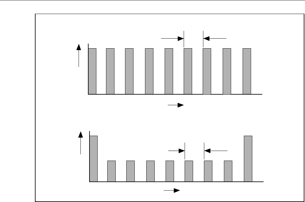
5700A/5720A Series II Calibrator
Service Manual
1-10
COST $ COST $
CALIBRATION CYCLE
CALIBRATION CYCLE
TRADITIONAL CALIBRATOR CALIBRATION
5700A/5720A SERIES II CALIBRATION
TIME
TIME
f1-1.eps
Figure 1-1. Time and Costs: Calibrator Calibration
1-17. The Calibration Process
Calibration requires only three external standards: 10V, 1Ω, and 10 kΩ.
Environmentally-controlled internal check standards provide the primary reference
points. A stored table of calibration constants defines additional reference points for
controlling the output. Traceable calibration and adjustment to the specified level of
performance is accomplished in a semi-automated process that revises this table.
When you finish calibration, but before you save the new constants, the calibrator
presents you with the proposed adjustments as +/- ppm of range and percentage change
in specification for each range and function. You can print a list of changes through the
serial (RS-232C) port, or send them to a computer through either the serial port or the
IEEE-488 port. Also on completion of calibration, the calibrator displays the largest
proposed change.
Calibration can be completed as far as deriving and printing the proposed adjustments
without changing the setting of the rear panel CALIBRATION switch; however, the
switch must be set to ENABLE to store the changes in nonvolatile memory and make
them effective. The switch is recessed to allow the metrologist to cover it with a
calibration sticker to guarantee calibrator integrity.
1-18. Establishing Traceability
Traceability to national standards is established as follows:

Introduction and Specifications
Calibration Check
1
1-11
• Except for the internal ac/dc transfer standard, the internal check standards are
directly calibrated by traceable external standards every time the 5700A/5720A
Series II is calibrated.
• The internal ac/dc transfer standard is never adjusted, so its traceability is not
disturbed by calibration. Infrequent verification is done in the traditional way, by
comparing selected ac voltage outputs with an external dc voltage standard through
an external ac/dc transfer standard. Fluke recommends this be done every two years,
or as determined by the policy of your organization.
• Infrequent independent verification is also performed on stable parameters, such as
frequency flatness, determined more by circuit geometry and dielectric constants
than time.
1-19. Calibration Reports
The calibrator stores two sets of calibration constants: the set currently in use and the old
set from the previous calibration. This gives the calibrator the ability at any time to
produce a calibration report of the differences between the present settings and the
settings that were in effect before the last calibration. The report shows changes for each
range and function in +/- ppm of range and in percentage of specification limit. You can
print the report or send it to a host computer through either the RS-232-C or IEEE-488
interface.
If you request a calibration report after doing calibration but before saving the new
constants, the report shows proposed changes to the calibration constants relative to the
previously stored settings.
1-20. Calibration Check
Checking the calibration takes about an hour, and provides you with a means of
documenting the calibrator’s performance of a between calibrations. Calibration
checking is similar to calibration, except internal check standards are used as primary
references (no external standards are needed), and changes cannot be stored. The process
produces a report similar to normal calibration, showing drift relative to internal check
standards. Because cal check does not change stored calibration constants, there is no
need to enable the rear panel CALIBRATION switch. Therefore, an external computer
can do the procedure unattended.
1-21. Developing a Performance History
A Fluke specification is a set of performance limits that all products must meet. To
maintain consistent quality, Fluke calibrators are specified with enough margin to
include temperature, line, and load extremes, plus additional margin for production. This
means that a typical 5700A/5720A Series II calibrator in a typical environment operates
inside 50% of specification limits. For some exacting applications, it can be helpful to
know just how accurately a particular calibrator operates. The proper way to do this is to
accumulate a performance history by calibrating regularly and recording results on a
control chart.
Calibrating regularly and recording the results on a control chart is tedious and requires a
large array of equipment. The calibrator’s calibration check feature is an alternative with
some distinct advantages:
• Calibrated check standards are already programmed into the unit. You do not have to
use external standards.

5700A/5720A Series II Calibrator
Service Manual
1-12
• The process is consistent and automatic: it does not require an operator’s assistance.
Each calibration check produces a new set of data points for accumulating a historical
record. When this process is externally automated, significant history can be
accumulated much faster than with a manual calibration.
1-22. Range Calibration
After calibration, you can make further fine adjustments to each range. Range
adjustments are optional; they are not necessary to meet total uncertainty specifications.
However, they do allow you to align your calibrator closer to your standards.
Before you do range calibration, you must first use the calibrator’s semi-automated
calibration procedure. This is to calibrate the ranges that will not be adjusted. It also
performs an initial adjustment for each range, and supplies flatness corrections for ac
functions.
1-23. DC Zeros Calibration
To ensure the validity of the specifications, a dc zeros calibration must be performed at
least every 30 days. If more than 30 days elapse without a dc zeros calibraiton a warning
message appears. This procedure does not require any external equipment or connections
and takes approximately 2.5 minutes to complete.
1-24. Specifications
The 5700A/5720A Series II calibrators are verified and calibrated at the factory prior to
shipment to ensure they meet the accuracy standards required for all certified calibration
laboratories. By calibrating to the specifications in this chapter, you can maintain the
high performance level throughout the life of your calibrator.
Specifications are valid after a warm-up period of twice the time the calibrator has been
turned off, up to a maximum of 30 minutes. For example, if the calibrator has been
turned off for five minutes, the warm-up period is ten minutes.
1-25. Specification Confidence Levels
You calibrator’s performance level is ensured by regular calibration to the primary
performance specifications, which are provided at both the 99% and 95% confidence
levels. The 95% confidence level will provide an accuracy that surpasses the accuracy
requirements for meeting Tag 4 standards, or a coverage factor of 2. Calibration at the
99% confidence level is also available for those applications that require a confidence
factor for the specifications that is higher than 95%. For information on selecting the
confidence level, refer to Chapter 4.
The tables in this chapter provide specifications at both the 95% and 99% confidence
levels for the 5700A/5720A Series II calibrators. Included with these tables are operating
specifications for using the calibrator with the Wideband AC Module (Option 5700A-03)
and the 5725A Amplifier.
1-26. Using Absolute and Relative Uncertainty Specifications
To evaluate the 5700A/5720A Series II coverage of your calibration workload, use the
Absolute Uncertainty specifications. Absolute uncertainty includes stability, temperature
coefficient, linearity, line and load regulation, and the traceability to external standards.

Introduction and Specifications
Specifications
1
1-13
You do not need to add anything to absolute uncertainty to determine the ratios between
the calibrator’s uncertainties and the uncertainties of your calibration workload.
Relative uncertainty specifications are provided for enhanced accuracy applications.
These specifications apply when range constants are adjusted (see “Range Calibration”).
To calculate absolute uncertainty, you must combine the uncertainties of your external
standards and techniques with relative uncertainty.
1-27. Using Secondary Performance Specifications
Secondary performance specifications and operating characteristics are included in
uncertainty specifications. They are provided for special calibration requirements such as
stability or linearity testing.
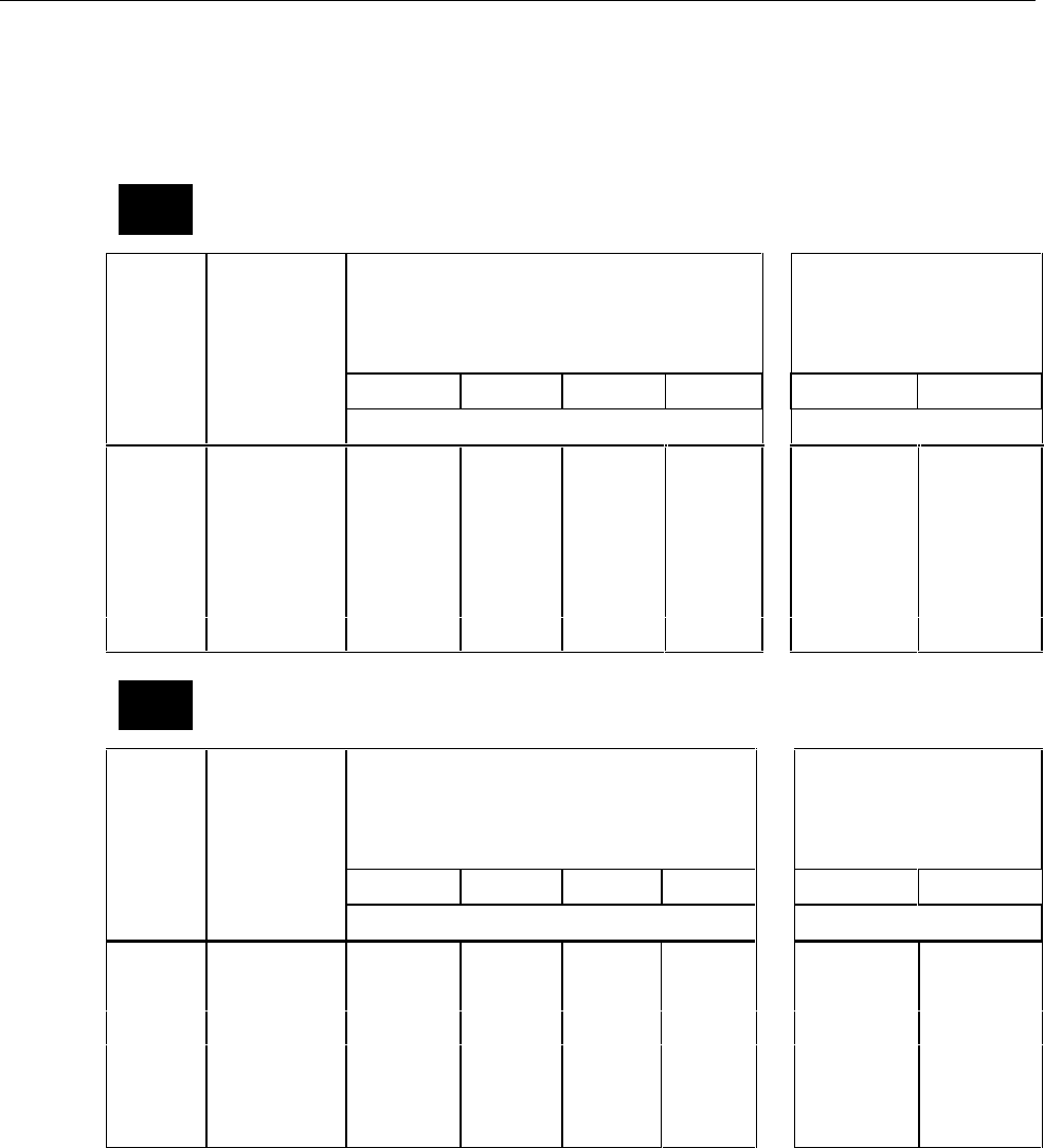
5700A/5720A Series II Calibrator
Service Manual
1-14
1-28. DC Voltage Specifications
Table 1-2. 5720A Series II DC Voltage Specifications: 99 % and 95 % Confidence Levels
5720A
99%
99 % Confidence Level
Range Resolution
Absolute Uncertainty
± 5 °C from calibration temperature
For fields strengths >1 V/m but ≤3 V/m,
add 0.01% of range.
Relative Uncertainty
± 1 °C
24 Hours 90 Days 180 Days 1 Year 24 Hours 90 Days
± (ppm output + µV) ± (ppm output + µV)
220 mV 10 nV 0 5 + 0.5 7 + 0.5 0 8 + 0.5 0 9 + 0.5 0 2 + 0.4 2.5 + 0.4
2.2 V 100 nV 3.5 + 0.8 4 + 0.8 4.5 + 0.8 0 6 + 0.8 0 2 + 0.8 2.5 + 0.8
11 V 1 µV 2.5 + 3 3 + 3 3.5 + 3 0 4 + 3 0 1 + 3 1.5 + 3
22 V 1 µV 2.5 + 5 3 + 5 3.5 + 5 0 4 + 5 0 1 + 5 1.5 + 5
220 V 10 µV 3.5 + 50 4 + 50 0 5 + 50 06 + 50 02 + 50 2.5 + 50
1100 V 100 µV0 5 + 500 6 + 500 0 7 + 500 08 + 500 2.5 + 400 03 + 400
5720A
95%
95% Confidence Level
Range Resolution
Absolute Uncertainty
± 5 °C from calibration temperature
For fields strengths >1 V/m but ≤3 V/m,
add 0.01 % of range.
Relative Uncertainty
± 1 °C
24 Hours 90 Days 180 Days 1 Year 24 Hours 90 Days
± (ppm output + µV) ± (ppm output + µV)
220 mV 10 nV 4 + 0.4 0 6 + 0.4 6.5 + 0.4 7.5 + 0.4 1.6 + 0.4 02 + 0.4
2.2 V 100 nV 3 + 0.7 3.5 + 0.7 0 4 + 0.7 05 + 0.7 1.6 + 0.7 02 + 0.7
11 V 1 µV 2 + 2.5 2.5 + 2.5 03 + 2.5 3.5 + 2.5 0.8 + 2.5 1.2 + 2.5
22 V 1 µV 2 + 4 2.5 + 4 03 + 4 3.5 + 4 0.8 + 4 1.2 + 4
220 V 10 µV 3 + 40 3.5 + 40 04 + 40 0 5 + 40 1.6 + 40 02 + 40
1100 V 100 µV 4 + 400 4.5 + 400 06 + 400 6.5 + 400 02 + 400 2.4 + 400
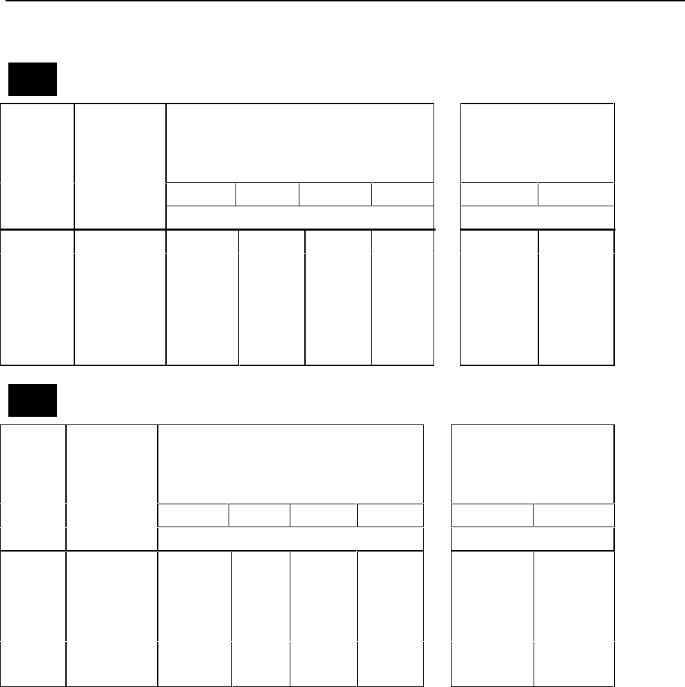
Introduction and Specifications
DC Voltage Specifications
1
1-15
Table 1-3. 5700A Series II DC Voltage Specifications: 99 % and 95 % Confidence Levels
5700A
99%
99 % Confidence Level
Range Resolution
Absolute Uncertainty
± 5 °C from calibration temperature
For fields strengths >1 V/m but ≤3 V/m,
add 0.01 % of range.
Relative Uncertainty
± 1 °C
24 Hours 90 Days 180 Days 1 Year 24 Hours 90 Days
± (ppm output + µV) ± (ppm output + µV)
220 mV 10 nV 6.5 + .75 7 + .75 08 + .75 09 + .8 2.5 + .5 04 + .5
2.2 V 100 nV 3.5 + 1.2 6 + 1.2 07 + 1.2 08 + 1.2 2.5 + 1.2 04 + 1.2
11 V 1 µV 3.5 + 3 5 + 4 07 + 4 08 + 4 1.5 + 3 3.5 + 4
22 V 1 µV 3.5 + 6 5 + 8 07 + 8 08 + 8 1.5 + 6 3.5 + 8
220 V 10 µV 05 + 100 6 + 100 08 + 100 09 + 100 2.5 + 100 04 + 100
1100 V 100 µV 07 + 600 8 + 600 10 + 600 11 + 600 03 + 600 4.5 + 600
5700A
95%
95 % Confidence Level
Range Resolution
Absolute Uncertainty
± 5 °C from calibration temperature
For fields strengths >1 V/m but ≤3 V/m,
add 0.01 % of range.
Relative Uncertainty
± 1 °C
24 Hours 90 Days 180 Days 1 Year 24 Hours 90 Days
± (ppm output + µV) ± (ppm output + µV)
220 mV 10 nV 5.5 + 0.6 6 + 0.6 7 + 0.6 8 + 0.6 02 + 0.4 3.5 + 0.4
2.2 V 100 nV 3.5 + 1 5 + 1 6 + 1 7 + 1 02 + 1 3.5 + 1
11 V 1 mV 03 + 3.5 4 + 3.5 6 + 3.5 7 + 3.5 1.2 + 3 03 + 3.5
22 V 1 mV 03 + 6.5 4 + 6.5 6 + 6.5 7 + 6.5 1.2 + 6 03 + 7
220 V 10 mV 04 + 80 5 + 80 7 + 80 8 + 80 02 + 80 3.5 + 80
1100 V 100 mV 06 + 500 7 + 500 8 + 500 9 + 500 2.4 + 500 04 + 500

5700A/5720A Series II Calibrator
Service Manual
1-16
Table 1-4. DC Voltage Secondary Performance Specifications and Operating Characteristics
Temperature Coefficient
Adder [Note 2] Noise
Range Stability [Note 1]
± 1 °C 10 °-40 °C 0 °-10 °C
and Linearity
± 1 °C Bandwidth
0.1-10 Hz Bandwidth
10 Hz-10 kHz
24 Hours 40°-50 °C pk-pk RMS
± (ppm output + µV) ± (ppm output + µV)/°C ± (ppm output + µV) µV
220 mV
2.2 V
11 V
22 V
220 V
1100 V
0.3 + 0.3
0.3 + 1
0.3 + 2.5
0.4 + 5
0.5 + 40
0.5 + 200
00.4 + 0.1
00.3 + 0.1
0.15 + 0.2
00.2 + 0.4
00.3 + 5
00.5 + 10
1.5 + 0.5
1.5 + 2
0 1 + 1.5
1.5 + 3
1.5 + 40
0 3 + 200
0 1 + 0.2
0 1 + 0.6
0.3 + 2
0.3 + 4
0 1 + 40
0 1 + 200
0.15 + 0.1
0.15 + 0.4
0.15 + 2
0.15 + 4
0.15 + 60
0.15 + 300
5
15
50
50
150
500
Notes:
1. Stability specifications are included in the Absolute Uncertainty values in the primary specification
tables.
2. Temperature coefficient is an adder to uncertainty specifications that does
not
apply unless operating
more than ±5 °C from calibration temperature.
Minimum output: 0 V for all ranges, except 100 V for 1100 V range
Maximum load: 50 mA for 2.2 V through 220 V ranges; 20 mA for 1100 V range; 50 Ω output impedance
on 220 mV range; all ranges <1000 pF, >25 Ω
Load regulation: <(0.2 ppm of output + 0.1ppm of range), full load to no load
Line regulation: <0.1 ppm change, ± 10 % of selected nominal line
Settling time: 3 seconds to full accuracy; + 1 second for range or polarity change; + 1 second for 1100 V
range
Overshoot: <5 %
Common mode rejection: 140 dB, DC to 400 Hz
Remote sensing: Available 0 V to ±1100 V, on 2.2 V through 1100 V ranges

Introduction and Specifications
AC Voltage Specifications
1
1-17
1-29. AC Voltage Specifications
Table 1-5. 5720A Series II AC Voltage Specifications: 99 % Confidence Level
5720A
99%
99 % Confidence Level
Range Resolution Frequency Absolute Uncertainty
± 5 °C from calibration temperature Relative Uncertainty
± 1 °C
24 Hours 90 Days 180 Days 1 Year 24 Hours 90 Days
Hz ± (ppm output + µV) ± (ppm output + µV)
2.2 mV 1 nV
0010 - 20
0020 - 40
0040 - 20 k
020 k - 50 k
050 k - 100 k
100 k - 300 k
300 k - 500 k
500 k - 1 M
0250 + 5
0100 + 5
0085 + 5
0220 + 5
0500 + 6
1000 + 12
1400 + 25
2900 + 25
0270 + 5
0105 + 5
0090 + 5
0230 + 5
0540 + 6
1200 + 12
1500 + 25
3100 + 25
0290 + 5
0110 + 5
0095 + 5
0240 + 5
0570 + 6
1250 + 12
1600 + 25
3250 + 25
00300 + 5
00115 + 5
00100 + 5
00250 + 5
00600 + 6
01300 + 12
01700 + 25
03400 + 25
0250 + 5
0100 + 5
0060 + 5
0085 + 5
0200 + 6
0350 + 12
0800 + 25
2700 + 25
0270 + 5
0105 + 5
0065 + 5
0095 + 5
0220 + 6
0400 + 12
1000 + 25
3000 + 25
22 mV 10 nV
0010 - 20
0020 - 40
0040 - 20 k
020 k - 50 k
050 k - 100 k
100 k - 300 k
300 k - 500 k
500 k - 1 M
0250 + 5
0100 + 5
0085 + 5
0220 + 5
0500 + 6
1000 + 12
1400 + 25
2900 + 25
0270 + 5
0105 + 5
0090 + 5
0230 + 5
0540 + 6
1200 + 12
1500 + 25
3100 + 25
0290 + 5
0110 + 5
0095 + 5
0240 + 5
0570 + 6
1250 + 12
1600 + 25
3250 + 25
00300 + 5
00115 + 5
00100 + 5
00250 + 5
00600 + 6
01300 + 12
01700 + 25
03400 + 25
0250 + 5
0100 + 5
0060 + 5
0085 + 5
0200 + 6
0350 + 12
0800 + 25
2700 + 25
0270 + 5
0105 + 5
0065 + 5
0095 + 5
0220 + 6
0400 + 12
1000 + 25
3000 + 25
220 mV 100 nV
0010 - 20
0020 - 40
0040 - 20 k
020 k - 50 k
050 k - 100 k
100 k - 300 k
300 k - 500 k
500 k - 1 M
0250 + 15
0100 + 8
0085 + 8
0220 + 8
0500 + 20
0850 + 25
1400 + 30
2700 + 60
0270 + 15
0105 + 8
0090 + 8
0230 + 8
0540 + 20
0900 + 25
1500 + 30
2900 + 60
0290 + 15
0110 + 8
0095 + 8
0240 + 8
0570 + 20
1000 + 25
1600 + 30
3100 + 60
00300 + 15
00115 + 8
00100 + 8
00250 + 8
00600 + 20
01100 + 25
01700 + 30
03300 + 60
0250 + 15
0100 + 8
0060 + 8
0085 + 8
0200 + 20
0350 + 25
0800 + 30
2600 + 60
0270 + 15
0105 + 8
0065 + 8
0095 + 8
0220 + 20
0400 + 25
1000 + 30
2800 + 60
2.2 V 1 mV
0010 - 20
0020 - 40
0040 - 20 k
020 k - 50 k
050 k - 100 k
100 k - 300 k
300 k - 500 k
500 k - 1 M
0250 + 50
0095 + 20
0045 + 10
0080 + 12
0120 + 40
0380 + 100
1000 + 250
1600 + 400
0270 + 50
0100 + 20
0047 + 10
0085 + 12
0125 + 40
0420 + 100
1100 + 250
1800 + 600
0290 + 50
0105 + 20
0050 + 10
0087 + 12
0127 + 40
0460 + 100
1150 + 250
1900 + 400
00300 + 50
00110 + 20
00052 + 10
00090 + 12
00130 + 40
00500 + 100
01200 + 250
02000 + 400
0250 + 50
0095 + 20
0030 + 10
0070 + 12
0100 + 40
0270 + 100
0900 + 250
1200 + 400
0270 + 50
0100 + 20
0040 + 10
0075 + 12
0105 + 40
0290 + 100
1000 + 250
1300 + 400
22 V 10 mV
0010 - 20
0020 - 40
0040 - 20 k
020 k - 50 k
050 k - 100 k
100 k - 300 k
300 k - 500 k
500 k - 1 M
0250 + 500
0095 + 200
0045 + 70
0080 + 120
0110 + 250
0300 + 800
1000 + 2500
1500 + 4000
0270 + 500
0100 + 200
0047 + 70
0085 + 120
0115 + 250
0310 + 800
1100 + 2500
1600 + 4000
0290 + 500
0105 + 200
0050 + 70
0087 + 120
0117 + 250
0320 + 800
1150 + 2500
1700 + 4000
00300 + 500
00110 + 200
00052 + 70
00090 + 120
00120 + 250
00325 + 800
01200 + 2500
01800 + 4000
0250 + 500
0095 + 200
0030 + 70
0070 + 120
0100 + 250
0270 + 800
0900 + 2500
1300 + 4000
0270 + 500
0100 + 200
0040 + 70
0075 + 120
0105 + 250
0290 + 800
1000 + 2500
1400 + 4000
± (ppm output + mV) ± (ppm output + mV)
220 V
[Note 2] 100 mV
0010 - 20
0020 - 40
0040 - 20 k
020 k - 50 k
050 k - 100 k
100 k - 300 k
300 k - 500 k
500 k - 1 M
0250 + 5
0095 + 2
0057 + 0.7
0090 + 1.2
0160 + 3
0900 + 20
5000 + 50
8000 + 100
0270 + 5
0100 + 2
0060 + 0.7
0095 + 1.2
0170 + 3
1000 + 20
5200 + 50
9000 + 100
0290 + 5
0105 + 2
0062 + 0.7
0097 + 1.2
0175 + 3
1050 + 20
5300 + 50
9500 + 100
00300 + 5
00110 + 2
00065 + 0.7
00100 + 1.2
00 180 + 3
0 1100 + 20
0 5400 + 50
10,000 + 100
0250 + 5
0095 + 2
0045 + 0.7
0075 + 1.2
0140 + 3
0600 + 20
4500 + 50
8000 + 100
0270 + 5
0100 + 2
0050 + 0.7
0080 + 1.2
0150 + 3
0700 + 20
4700 + 50
8500 + 100
1100 V 1 mV
[Note 1] 0015 - 50
0050 - 1 k 0300 + 20
0070 + 4 0320 + 20
0075 + 4 0340 + 20
0080 + 4 00 360 + 20
00085 + 4 0300 + 20
0050 + 4 0320 + 20
0055 + 4
5725A Amplifier:
1100 V
1 mV
0040 - 1 k
001 k - 20 k
020 k - 30 k
0075 + 4
0105 + 6
0230 + 11
0080 + 4
0125 + 6
0360 + 11
0085 + 4
0135 + 6
0440 + 11
000 90 + 4
00 165 + 6
00 600 + 11
0050 + 4
0085 + 6
0160 + 11
0055 + 4
0105 + 6
0320 + 11
750 V 030 k - 50 k
050 k - 100k 0230 + 11
0600 + 45 0360 + 11
1300 + 45 0440 + 11
1600 + 45 00600 + 11
02300 + 45 0160 + 11
0380 + 45 0320 + 11
1200 + 45
Notes: 1. Maximum output 250V from 15-50 Hz.
2. See Volt-Hertz capability in Figure 1-2.

5700A/5720A Series II Calibrator
Service Manual
1-18
Table 1-6. 5720A Series II AC Voltage Specifications: 95 % Confidence Level
5720A
95%
95 % Confidence Level
Range Resolution Frequency Absolute Uncertainty
± 5 °C from calibration temperature Relative Uncertainty
± 1 °C
24 Hours 90 Days 180 Days 1 Year 24 Hours 90 Days
Hz ± (ppm output + µV) ± (ppm output + µV)
2.2 mV 1 nV
0010 - 20
0020 - 40
0040 - 20 k
020 k - 50 k
050 k - 100 k
100 k - 300 k
300 k - 500 k
500 k - 1 M
0200 + 4
0080 + 4
0070 + 4
0170 + 4
0400 + 5
0300 + 10
1100 + 20
2400 + 20
0220 + 4
0085 + 4
0075 + 4
0180 + 4
0460 + 5
0900 + 10
1200 + 20
2500 + 20
0230 + 4
0087 + 4
0077 + 4
0190 + 4
0480 + 5
1000 + 10
1300 + 20
2600 + 20
0240 + 4
0090 + 4
0080 + 4
0200 + 4
0500 + 5
1050 + 10
1400 + 20
2700 + 20
0200 + 4
0080 + 4
0050 + 4
0070 + 4
0160 + 5
0280 + 10
0650 + 20
2100 + 20
0220 + 4
0085 + 4
0055 + 4
0080 + 4
0180 + 5
0320 + 10
0800 + 20
2400 + 20
22 mV 10 nV
0010 - 20
0020 - 40
0040 - 20 k
020 k - 50 k
050 k - 100 k
100 k - 300 k
300 k - 500 k
500 k - 1 M
0200 + 4
0080 + 4
0070 + 4
0170 + 4
0400 + 5
0300 + 10
1100 + 20
2400 + 20
0220 + 4
0085 + 4
0075 + 4
0180 + 4
0460 + 5
0900 + 10
1200 + 20
2500 + 20
0230 + 4
0087 + 4
0077 + 4
0190 + 4
0480 + 5
1000 + 10
1300 + 20
2600 + 20
0240 + 4
0090 + 4
0080 + 4
0200 + 4
0500 + 5
1050 + 10
1400 + 20
2700 + 20
0200 + 4
0080 + 4
0050 + 4
0070 + 4
0160 + 5
0280 + 10
0650 + 20
2100 + 20
0220 + 4
0085 + 4
0055 + 4
0080 + 4
0180 + 5
0320 + 10
0800 + 20
2400 + 20
220 mV 100 nV
0010 - 20
0020 - 40
0040 - 20 k
020 k - 50 k
050 k - 100 k
100 k - 300 k
300 k - 500 k
500 k - 1 M
0200 + 12
0080 + 7
0070 + 7
0170 + 7
0400 + 17
0700 + 20
1100 + 25
2400 + 45
0220 + 12
0085 + 7
0075 + 7
0180 + 7
0420 + 17
0750 + 20
1200 +25
2500 + 45
0230 + 12
0087 + 7
0077 + 7
0190 + 7
0440 + 17
0800 + 20
1300 + 25
2600 + 45
0240 + 12
0090 + 7
0080 + 7
0200 + 7
0460 + 17
0900 + 20
1400 + 25
2700 + 45
0200 + 12
0080 + 7
0050 + 7
0070 + 7
0160 + 17
0280 + 20
0650 + 25
2100 + 45
0220 + 12
0085 + 7
0055 + 7
0080 + 7
0180 + 17
0320 + 20
0800 + 25
2400 + 45
2.2 V 1 mV
00010 - 20
0020 - 40
0040 - 20 k
020 k - 50 k
050 k - 100 k
100 k - 300 k
300 k - 500 k
500 k - 1 M
0200 + 40
0075 + 15
0037 + 8
0065 + 10
0100 + 30
0300 + 80
0800 + 200
1300 + 300
0220 + 40
0080 + 15
0040 + 8
0070 + 10
0105 + 30
0340 + 80
0900 + 200
1500 + 300
0230 + 40
0085 + 15
0042 + 8
0073 + 10
0107 + 30
0380 + 80
0950 + 200
1600 + 300
0240 + 40
0090 + 15
0045 + 8
0075 + 10
0110 + 30
0420 + 80
1000 + 200
1700 + 300
0200 + 40
0075 + 15
0025 + 8
0055 + 10
0080 + 30
0230 + 80
0700 + 200
1000 + 300
0220 + 40
0080 + 15
0035 + 8
0060 + 10
0085 + 30
0250 + 80
0800 + 200
1100 + 300
22V 10 mV
0010 - 20
0020 - 40
0040 - 20k
020k - 50k
050k - 100k
100k - 300k
300k - 500k
500k - 1M
0200 + 400
0075 + 150
0037 + 50
0065 + 100
0090 + 200
0250 + 600
0800 + 2000
1200 + 3200
0220 + 400
0080 + 150
0040 + 50
0070 + 100
0095 + 200
0260 + 600
0900 + 2000
1300 + 3200
0230 + 400
0085 + 150
0042 + 50
0073 + 100
0097 + 200
0270 + 600
0900 + 2000
1400 + 3200
0240 + 400
0090 + 150
0045 + 50
0075 + 100
0100 + 200
0275 + 600
1000 + 2000
1500 + 3200
0200 + 400
0075 + 150
0025 + 50
0055 + 100
0080 + 200
0250 + 600
0700 + 2000
1100 + 3200
0220 + 400
0080 + 150
0035 + 50
0060 + 100
0085 + 200
0270 + 600
0800 + 2000
1200 + 3200
± (ppm output + mV) ± (ppm output + mV)
220 V
[Note 2] 100 mV
0010 - 20
0020 - 40
0040 - 20 k
020 k - 50 k
050 k - 100 k
100 k - 300 k
300 k - 500 k
500 k - 1 M
0200 +4
0075 + 1.5
0045 + 0.6
0070 + 1
0120 + 2.5
0700 + 16
4000 + 40
6000 + 80
0220 + 4
0080 + 1.5
0047 + 0.6
0075 + 1
0130 + 2.5
0800 + 16
4200 + 40
7000 + 80
0230 + 4
0085 + 1.5
0050 + 0.6
0077 + 1
0140 + 2.5
0850 + 16
4300 + 40
7500 + 80
0240 + 4
0090 + 1.5
0052 + 0.6
0080 + 1
0150 + 2.5
0900 + 16
4400 + 40
8000 + 80
0200 + 4
0075 + 1.5
0035 + 0.6
0060 + 1
0110 + 2.5
0500 + 16
3600 + 40
6500 + 80
0220 + 4
0080 + 1.5
0040 + 0.6
0065 + 1
0120 + 2.5
0600 + 16
3800 + 40
7000 + 80
1100 V 1 mV
[Note 1] 0015 - 50
0050 - 1 k 0240 + 16
0055 + 3.5 0260 + 16
0060 + 3.5 0280 + 16
0065 + 3.5 0300 + 16
0070 + 3.5 0240 + 16
0040 + 3.5 0260 + 16
0045 + 3.5
5725A Amplifier:
1100 V
1 mV
0040 - 1 k
001 k - 20 k
020 k - 30 k
0075 + 4
0105 + 6
0230 + 11
0080 + 4
0125 + 6
0360 + 11
0085 + 4
0135 + 6
0440 + 11
0090 + 4
0165 + 6
0600 + 11
0050 + 4
0085 + 6
0160 + 11
0055 + 4
0105 + 6
0320 + 11
750 V 030 k - 50 k
050 k - 100 k 0230 + 11
0600 + 45 0360 + 11
1300 + 45 0440 + 11
1600 + 45 0600 + 11
2300 + 45 0160 + 11
0380 + 45 0320 + 11
1200 + 45
Notes: 1. Maximum output 250V from 15-50 Hz.
2. See Volt-Hertz capability in Figure 1-2.

Introduction and Specifications
AC Voltage Specifications
1
1-19
Table 1-7. 5700A Series II AC Voltage Specifications: 99 % Confidence Level
5700A
99%
99 % Confidence Level
Range Resolution Frequency Absolute Uncertainty
± 5 °C from calibration temperature Relative Uncertainty
± 1 °C
24 Hours 90 Days 180 Days 1 Year 24 Hours 90 Days
Hz ± (ppm output + µV) ± (ppm output + µV)
2.2 mV 1 nV 0010 - 20
0020 - 40
0040 - 20 k
020 k - 50 k
050 k - 100 k
100 k - 300 k
300 k - 500 k
500 k - 1 M
0
0 500 + 5
00200 + 5
0
0 100 + 5
0
0 340 + 5
0
0 800 + 8
01100 + 15
01500 + 30
0
4000 + 40
0
0 550 + 5
0
0 220 + 5
0
0 110 + 5
0
0 370 + 5
0
0 900 + 8
01200 + 15
01700 + 30
04400 + 40
0
0 600 + 5
0
0 230 + 5
0
0 120 + 5
0
0 390 + 5
0
0 950 + 8
0
1300 + 15
01700 + 30
0
4700 + 40
0
0 600 + 5
0
0 240 + 5
0
0 120 + 5
0
0 410 + 5
0
0950 + 8
0
1300 + 15
0
1800 + 30
0
4800 + 40
00 500 + 5
00 200 + 5
000 60 + 5
00 100 + 5
00 220 + 8
00 400 + 15
01000 + 30
00 400 + 30
0
0 550 + 5
0
0220 + 5
0
0 065 + 5
0
0 110 + 5
0
0 240 + 8
0
0 440 + 15
0
1100 + 30
0
4400 + 30
22 mV 10 nV 0010 - 20
0020 - 40
0040 - 20 k
020 k - 50 k
050 k - 100 k
100 k - 300 k
300 k - 500 k
500 k - 1 M
0
0 500 + 6
0
0 200 + 6
0
0100 + 6
0
0340 + 6
0
0800 + 8
0
1100 + 15
01500 + 30
04000 + 40
0
0 550 + 6
0
0 220 + 6
0
0 110 + 6
0
0 370 + 6
0
0 900 + 8
01200 + 15
01700 + 30
04400 + 40
00600 + 6
0
0 230 + 6
0
0 120 + 6
0
0 390 + 6
0
0 950 + 8
0
1300 + 15
0
1700 + 30
0
4700 + 40
0
0600 + 6
0
0 240 + 6
0
0 120 + 6
0
0 410 + 6
0
0 950 + 8
0
1300 + 15
0
1800 + 30
0
4800 + 40
00 500 + 6
00 200 + 6
000 60 + 6
00 100 + 6
00 220 + 8
00 400 + 15
01000 + 30
0 4000 + 30
0
0 550 + 6
0
0 220 + 6
0
00 65 + 6
0
0 110 + 6
0
0 240 + 8
0
0 440 + 15
0
1100 + 30
0
4400 + 30
220 mV 100 nV 0010 - 20
0020 - 40
0040 - 20 k
020 k - 50 k
050 k - 100 k
100 k - 300 k
300 k - 500 k
500 k - 1 M
0
0500 + 16
0
0 200 + 10
0
0 095 + 10
0
0 300 + 10
0
0 750 + 30
0
0 940 + 30
0
1500 + 40
0
3000 + 100
0
0 550 + 16
0
0 220 + 10
0
0 100 + 10
0
0 330 + 10
0
0 800 + 30
0
1000 + 30
01700 + 40
03300 + 100
0
0 600 + 16
0
0 230 + 10
0
0 110 + 10
0
0 350 + 10
0
0 850 + 30
01100 + 30
0
1700 + 40
0
3500 + 100
0
0 600 + 16
00240 + 10
00110 + 10
00360 + 10
0
0900 + 30
01100 + 30
01800 + 40
03600 + 100
00 500 + 16
00200 + 10
00060 + 10
00100 + 10
00220 + 30
00400 + 30
01000 + 40
03000 + 100
00550 + 16
00220 + 10
00065 + 10
00110 + 10
00240 + 30
00440 + 30
01100 + 40
03300 + 100
2.2 V 1 mV 0010 - 20
0020 - 40
0040 - 20 k
020 k - 50 k
050 k - 100 k
100 k - 300 k
300 k - 500 k
500 k - 1 M
0
0 500 + 100
0
0 150 + 30
0
00 70 + 7
0
0 120 + 20
0
0 230 + 80
0
0 400 + 150
0
1000 + 400
0
2000 + 1000
0
0 550 + 100
0
0 170 + 30
0
00 75 + 7
0
0 130 + 20
0
0 250 + 80
0
0 440 + 150
0
1100 + 400
0
2200 + 1000
0
0 600 + 100
0
0 170 + 30
0
00 80 + 7
0
0 140 + 20
0
0 270 + 80
0
0 470 + 150
0
1200 + 400
0
2300 + 1000
0
0 600 + 100
0
0 180 + 30
0
00 85 + 7
0
0 140 + 20
0
0 280 + 80
0
0 480 + 150
0
1200 + 400
0
2400 + 1000
00 500 + 100
00 150 + 30
000 40 + 7
00 100 + 20
00 200 + 80
00 400 + 150
0 1000 + 400
0 2000 + 1000
0
0 550 + 100
0
0 170 + 30
0
00 45 + 7
0
0 110 + 20
0
0 220 + 80
0
0 440 + 150
0
1100 + 400
0
2200 + 1000
22 V 10 mV 0010 - 20
0020 - 40
0040 - 20 k
020 k - 50 k
050 k - 100 k
100 k - 300 k
300 k - 500 k
500 k - 1 M
0
0 500 + 1000
0
0 150 + 300
0
00 70 + 70
0
0 120 + 200
0
0 230 + 400
0
0 500 + 1700
0
1200 + 5000
0
2600 + 9000
0
0 550 + 1000
0
0 170 + 300
0
00 75 + 70
0
0 130 + 200
0
0 250 + 400
0
0 550 + 1700
0
1300 + 5000
0
2800 + 9000
0
0 600 + 1000
0
0 170 + 300
0
00 80 + 70
0
0 140 + 200
0
0 270 + 400
0
0 550 + 1700
0
1300 + 5000
0
2900 + 9000
0
0 600 + 1000
0
0 180 + 300
0
00 85 + 70
0
0 140 + 200
0
0 280 + 400
0
0 600 + 1700
0
1400 + 5000
0
3000 + 9000
00 500 + 1000
00 150 + 300
000 40 + 70
00 100 + 200
00 200 + 400
00500 + 1700
01200 + 5000
02600 + 9000
0
0 550 + 1000
0
0 170 + 300
0
00 45 + 70
0
0 110 + 200
0
0 220 + 400
0
0 550 + 1700
0
1300 + 5000
0
2800 + 9000
± (ppm output + mV) ± (ppm output + mV)
220 V
[Note 2] 100 mV 0010 - 20
0020 - 40
0040 - 20 k
020 k - 50 k
050 k - 100 k
100 k - 300 k
300 k - 500 k
500 k - 1 M
0
0 500 + 10
0
0 150 + 3
0
00 75 + 1
0
0 200 + 4
0
0 500 + 10
0
1500 + 110
0
5000 + 110
12,000 + 220
0
0 550 + 10
0
0 170 + 3
0
00 80 + 1
0
0 220 + 4
0
0 550 + 10
0
1500 + 110
0
5200 + 110
12,500 + 220
0
0600 + 10
0
0 170 + 3
0
00 85 + 1
0
0 240 + 4
0
0 600 + 10
0
1600 + 110
0
5300 + 110
12,500 + 220
0
0 600 + 10
0
0 180 + 3
0
00 90 + 1
0
0 250 + 4
0
0 600 + 10
0
1600 + 110
0
5400 + 110
13,000 + 220
00 500 + 10
00 150 + 3
000 45 + 1
00 100 + 1
00 300 + 10
01500 + 110
0 5000 + 110
12,000 + 220
0
0 550 + 10
0
0 170 + 3
0
00 50 + 1
0
0 110 + 1
0
0 330 + 10
0
1500 + 100
0
5200 + 110
12,000 + 220
1100 V 1 mV
[Note 1] 00015 - 50
00050 - 1 k
0
0 400 + 20
0
00 75 + 4 00420 + 20
0
00 80 + 4 00440 + 20
0
00 85 + 4 00460 + 20
0
00 90 + 4 00400 + 20
000 50 + 4 00420 + 20
0
00 55 + 4
5725A Amplifier:
1100 V 1 mV 00040 - 1 k
0001 k - 20 k
0020 k - 30 k
0
00 75 + 4
0
0 105 + 6
0
0 230 + 11
0
00 80 + 4
0
0 125 + 6
0
0 360 + 11
0
00 85 + 4
0
0 135 + 6
0
0 440 + 11
0
00 90 + 4
0
0 165 + 6
0
0 600 + 11
000 50 + 4
000 85 + 6
00 160 + 11
0
00 55 + 4
0
0 105 + 6
0
0 320 + 11
750 V 0030 k - 50 k
0050 k - 100 k
0
0 230 + 11
0
0 600 + 45
0
0 360 + 11
0
1300 + 45
0
0 440 + 11
0
1600 + 45
0
0 600 + 11
0
2300 + 45 00 160 + 11
00 380 + 45
0
0 320 + 11
0
1200 + 45
Notes: 1. Maximum output 250V from 15-50 Hz.
2. See Volt-Hertz capability in Figure 1-2.

5700A/5720A Series II Calibrator
Service Manual
1-20
Table 1-8. 5700A Series II AC Voltage Specifications: 95 % Confidence Level
5700A
95%
95% Confidence Level
Range Resolution Frequency Absolute Uncertainty
± 5 °C from calibration temperature
Relative Uncertainty
± 1 °C
24 Hours 90 Days 180 Days 1 Year 24 Hours 90 Days
Hz ± (ppm output + µV) ± (ppm output + µV)
2.2 mV 1 nV
0010 - 20
0020 - 40
0040 - 20 k
020 k - 50 k
050 k - 100 k
100 k - 300 k
300 k - 500 k
500 k - 1 M
0
0 400 + 4.5
0
0 170 + 4.5
0
00 85 + 4.5
0
0 300 + 4.5
0
0 700 + 7
0
0 900 + 13
0
1300 + 25
0
2800 + 25
0
0 500 + 4.5
0
0 190 + 4.5
0
00 95 + 4.5
0
0 330 + 4.5
0
0750 + 7
0
1000 + 13
0
1500 + 25
0
3100 + 25
0
0 530 + 4.5
0
0 200 + 4.5
0
0 100 + 4.5
0
0 350 + 4.5
0
0 800 + 7
0
1050 + 13
0
1600 + 25
0
3300 + 25
0
0 550 + 4.5
0
0 210 + 4.5
0
0 105 + 4.5
0
0 370 + 4.5
0
0 850 + 7
0
1100 + 13
0
1700 + 25
0
3400 + 25
00 400 + 4.5
00 170 + 4.5
000 55 + 4.5
000 90 + 4.5
00 210 + 7
00 380 + 13
00 900 + 25
0 2900 + 25
0
0 500 + 4.5
0
0 190 + 4.5
0
00 60 + 4.5
0
0 100 + 4.5
0
0 230 + 7
0
0 420 + 13
0
1000 + 25
0
3200 + 25
22 mV 10 nV
0010 - 20
0020 - 40
0040 - 20 k
020 k - 50 k
050 k - 100 k
100 k - 300 k
300 k - 500 k
500 k - 1 M
0
0 400 + 5
0
0 170 + 5
0
00 85 + 5
0
0 300 + 5
0
0 700 + 7
0
0 900 + 12
0
1300 + 25
0
2800 + 25
0
0 500 + 5
0
0 190 + 5
0
00 95 + 5
0
0 330 + 5
0
0 750 + 7
0
1000 + 12
0
1500 + 25
0
3100 + 25
0
0 530 + 5
0
0 200 + 5
0
0 100 + 5
0
0 350 + 5
0
0 800 + 7
0
1050 + 12
0
1600 + 25
0
3300 + 25
0
0 550 + 5
0
0 210 + 5
0
0 105 + 5
0
0 370 + 5
0
0 850 + 7
0
1100 + 12
0
1700 + 25
0
3400 + 25
00 400 + 5
00 170 + 5
000 55 + 5
000 90 + 5
00 210 + 7
00 380 + 12
00900 + 25
0 2900 + 25
0
0 500 + 5
0
0 190 + 5
0
00 60 + 5
0
0 100 + 5
0
0 230 + 7
0
0 420 + 12
0
1000 + 25
0
3200 + 25
220 mV 100 nV
0010 - 20
0020 - 40
0040 - 20 k
020 k - 50 k
050 k - 100 k
100 k - 300 k
300 k - 500 k
500 k - 1 M
0
0 400 + 13
0
0 170 + 8
0
00 85 + 8
0
0 250 + 8
0
0 700 + 25
0
0 900 + 25
0
1300 + 35
0
2800 + 80
0
0 500 + 13
0
0 190 + 8
0
00 95 + 8
0
0 280 + 8
0
0 750 + 25
0
1000 + 25
0
1500 + 35
0
3100 + 80
0
0 530 + 13
0
0 200 + 8
0
0 100 + 8
0
0 300 + 8
0
0 800 + 25
0
1050 + 25
0
1600 + 35
0
3300 + 80
0
0 550 + 13
0
0 210 + 8
0
0 105 + 8
0
0 320 + 8
0
0 850 + 25
0
1100 + 25
0
1700 + 35
0
3400 + 80
00 400 + 13
00 170 + 8
000 55 + 8
000 90 + 8
00 210 + 25
00 380 + 25
00 900 + 35
0 2900 + 80
0
0 500 + 13
0
0 190 + 8
0
00 60 + 8
0
0 100 + 8
0
0 230 + 25
0
0 420 + 25
0
1000 + 35
0
3200 + 80
2.2 V 1 mV
0010 - 20
0020 - 40
0040 - 20 k
020 k - 50 k
050 k - 100 k
100 k - 300 k
300 k - 500 k
500 k - 1 M
0
0 400 + 80
0
0 130 + 25
0
00 60 + 6
0
0 105 + 16
0
0 190 + 70
0
0 350 + 130
0
0 850 + 350
0
1700 + 850
0
0 450 + 80
0
0 140 + 25
0
00 65 + 6
0
0 110 + 16
0
0 210 + 70
0
0 390 + 130
0
0950 + 350
0
1900 + 850
0
0 480 + 80
0
0 150 + 25
0
00 70 + 6
0
0 115 + 16
0
0 230 + 70
0
0 420 + 130
0
1000 + 350
0
2100 + 850
0
0 500 + 80
0
0 160 + 25
0
00 75 + 6
0
0 120 + 16
0
0 250 + 70
0
0 430 + 130
0
1050 + 350
0
2200 + 850
00 400 + 80
00 130 + 25
000 35 + 6
000 85 + 16
00 170 + 70
00 340 + 130
00 850 + 350
0 1700 + 850
0
0 450 + 80
0
0 140 + 25
0
00 40 + 6
0
00 95 + 16
0
0 190 + 70
0
0 380 + 130
0
0 950 + 350
0
1900 + 850
22 V 10 mV
0010 - 20
0020 - 40
0040 - 20 k
020 k - 50 k
050 k - 100 k
100 k - 300 k
300 k - 500 k
500 k - 1 M
0
0 400 + 800
0
0 130 + 250
0
00 60 + 60
0
0 105 + 160
0
0 190 + 350
0
0 400 + 1500
0
1050 + 4300
0
2300 + 8500
0
0 450 + 800
0
0 140 + 250
0
00 65 + 60
0
0 110 + 160
0
0 210 + 350
0
0 450 + 1500
0
1150 + 4300
0
2500 + 8500
0
0 480 + 800
0
0 150 + 250
0
00 70 + 60
0
0 115 + 160
0
0 230 + 350
0
0 470 + 1500
0
1200 + 4300
0
2600 + 8500
0
0 500 + 800
0
0 160 + 250
0
00 75 + 60
0
0 120 + 160
0
0 250 + 350
0
0 500 + 1500
0
1250 + 4300
0
2700 + 8500
00 400 + 800
00 130 + 250
000 35 + 60
000 85 + 160
00 170 + 350
00 400 + 1500
0 1000 + 4300
0 2200 + 8500
0
0 450 + 800
0
0 140 + 250
0
00 40 + 60
0
00 95 + 160
0
0 190 + 350
0
0 450 + 1500
0
1100 + 4300
0
2400 + 8500
± (ppm output + mV) ± (ppm output + mV)
220 V
[Note 2] 100 mV
0010 - 20
0020 - 40
0040 - 20 k
020 k - 50 k
050 k - 100 k
100 k - 300 k
300 k - 500 k
500 k - 1 M
0
0 400 + 8
0
0 130 + 2.5
0
00 65 + 0.8
0
0 170 + 3.5
0
0 400 + 8
0
1300 + 90
0
4300 + 90
10,500 + 190
0
0 450 + 8
0
0 140 + 2.5
0
00 70 + 0.8
0
0 190 + 3.5
0
0 450 + 8
0
1400 + 90
0
4500 + 90
11,000 + 190
0
0 480 + 8
0
0 150 + 2.5
0
00 75 + 0.8
0
0 210 + 3.5
0
0 480 + 8
0
1450 + 90
0
4600 + 90
11,300 + 190
0
0 500 + 8
0
0 160 + 2.5
0
00 80 + 0.8
0
0 220 + 3.5
0
0 500 + 8
0
1500 + 90
0
4700 + 90
11,500 + 190
00 400 + 8
00 130 + 2.5
000 40 + 0.8
000 85 + 3.5
00 270 + 8
0 1200 + 90
0 4200 + 90
10,500 + 190
0
0 450 + 8
0
0 140 + 2.5
0
00 45 + 0.8
0
00 95 + 3.5
0
0 300 + 8
0
1300 + 90
0
4500 + 90
11,000 + 190
1100 V 1 mV
[Note 1] 0015 - 50
0050 - 1 k
0
0 340 + 16
0
00 65 + 3.5 00360 + 16
0
00 70 + 3.5 00380 + 16
0
00 75 + 3.5 00400 + 16
0
00 80 + 3.5 00340 + 16
000 45 + 3.5 00360 + 16
0
00 50 + 3.5
5725A Amplifier:
1100 V 1 mV
0040 - 1 k
001 k - 20 k
020 k - 30 k
0
00 75 + 4
0
0 105 + 6
0
0 230 + 11
0
00 80 + 4
0
0 125 + 6
0
0 360 + 11
0
00 85 + 4
0
0 135 + 6
0
0 440 + 11
0
00 90 + 4
0
0 165 + 6
0
0 600 + 11
000 50 + 4
000 85 + 6
00 160 + 11
0
00 55 + 4
0
0 105 + 6
0
0 320 + 11
750 V 030 k - 50 k
050 k - 100 k
0
0 230 + 11
0
0 600 + 45
0
0 360 + 11
0
1300 + 45
0
0 440 + 11
0
1600 + 45
0
0 600 + 11
0
2300 + 45 00 160 + 11
00 380 + 45
0
0 320 + 11
0
1200 + 45
Notes: 1. Maximum output 250V from 15-50 Hz.
2. See Volt-Hertz capability in Figure 1-2.

Introduction and Specifications
AC Voltage Specifications
1
1-21
Table 1-9. AC Voltage Secondary Performance Specifications and Operating Characteristics
Stability
± 1 °C [Note 1] Temperature Coefficient Maximum
Distortion
Range Frequency 24 Hours 10°-40 °C 0°-10 °C and
40°-50 °C Output Impedance Bandwidth
10 Hz-10 MHz
Hz ± µV±µV/°C Ω± (% output + µV)
2.2 mV
0010 - 20
0020 - 40
0040 - 20 k
020 k - 50 k
050 k - 100 k
100 k - 300 k
300 k - 500 k
500 k - 1 M
5
5
2
2
3
3
5
5
0.05
0.05
0.05
0.1
0.2
0.3
0.4
0.5
0.05
0.05
0.05
0.1
0.2
0.3
0.4
0.5
50
00.05 + 10
0.035 + 10
0.035 + 10
0.035 + 10
0.035 + 10
000.3 + 30
000.3 + 30
000 1 + 30
22 mV
0010 - 20
0020 - 40
0040 - 20 k
020 k - 50 k
050 k - 100 k
100 k - 300 k
300 k - 500 k
500 k - 1 M
5
5
2
2
3
5
10
15
0.2
0.2
0.2
0.4
0.5
0.6
1
1
0.3
0.3
0.3
0.5
0.5
0.6
1
1
50
00.05 + 11
0.035 + 11
0.035 + 11
0.035 + 11
0.035 + 11
000.3 + 30
000.3 + 30
000 1 + 30
± (ppm output + µV) ± (ppm output µV)/°C
220 mV
0010 - 20
0020 - 40
0040 - 20 k
020 k - 50 k
050 k - 100 k
100 k - 300 k
300 k - 500 k
500 k - 1 M
150 + 20
080 + 15
012 + 2
010 + 2
010 + 2
020 + 4
100 + 10
200 + 20
002 + 1
002 + 1
002 + 1
015 + 2
015 + 4
080 + 5
080 + 5
080 + 5
02 + 1
02 + 1
02 + 1
15 + 2
15 + 4
80 + 5
80 + 5
80 + 5
50
00.05 + 16
0.035 + 16
0.035 + 16
0.035 + 16
0.035 + 16
000.3 + 30
000.3 + 30
000 1 + 30
Load Regulation
±(ppm output+ µV)
2.2 V
0010 - 20
0020 - 40
0040 - 20 k
020 k - 50 k
050 k - 100 k
100 k - 300 k
300 k - 500 k
500 k - 1 M
150 + 20
080 + 15
012 + 4
015 + 5
015 + 5
030 + 10
070 + 20
150 + 50
050 + 10
015 + 5
002 + 1
010 + 2
010 + 4
080 + 15
080 + 40
080 + 100
50 + 10
15 + 5
05 + 2
15 + 4
20 + 4
80 + 15
80 + 40
80 + 100
0010 + 2
0010 + 2
0010 + 4
0030 + 10
0120 + 16
0300 ppm
0600 ppm
01200 ppm
00.05 + 80
0.035 + 80
0.035 + 80
0.035 + 80
0.035 + 80
000.3 + 110
000.3 + 110
000 1 + 110
22 V
0010 - 20
0020 - 40
0040 - 20 k
020 k - 50 k
050 k - 100 k
100 k - 300 k
300 k - 500 k
500 k - 1 M
150 + 20
080 + 15
012 + 8
015 + 10
015 + 10
030 + 15
070 + 100
150 + 100
050 + 100
015 + 30
002 + 10
010 + 20
010 + 40
080 + 150
080 + 300
080 + 500
50 + 100
15 + 40
04 + 15
20 + 20
20 + 40
80 + 150
80 + 300
80 + 500
0010 + 20
0010 + 20
0010 + 30
0030 + 50
0080 + 80
0100 + 700
0200 + 1100
0600 + 3000
00.05 + 700
0.035 + 700
0.035 + 700
0.035 + 700
0.035 + 700
000.3 + 800
000.3 + 800
000 2 + 800
220 V
0010 - 20
0020 - 40
0040 - 20 k
020 k - 50 k
050 k - 100 k
100 k - 300 k
300 k - 500 k
500 k - 1 M
150 + 200
080 + 150
012 + 80
015 + 100
015 + 100
030 + 400
100 + 10,000
200 + 20,000
0 50 + 1000
0 15 + 300
00 2 + 80
0 10 + 100
0 10 + 500
0 80 + 600
0 80 + 800
0 80 + 1000
50 + 1000
15 + 300
04 + 80
20 + 100
20 + 500
80 + 600
80 + 800
80 + 1000
0010 + 200
0010 + 200
0010 + 300
0030 + .600
0080 + 3,000
0250 + 25,000
0500 + 50,000
1000 + 110,000
00.05 + 10,000
00.05 + 10,000
00.05 + 10,000
00.05 + 10,000
000.1 + 13,000
001.5 + 50,000
001.5 + 50,000
003.5 + 100,000
±(ppm output + mV) ±(ppm output)/°C ±(% output)
1100 V 0015 - 50
0050 - 1 k
150 + 0.5
020 + 0.5
50
2
50
5
0010 + 2
0010 + 1
0.15
0.07
Note: 1. Stability specifications are included in Absolute Uncertainty values for the primary specifications.
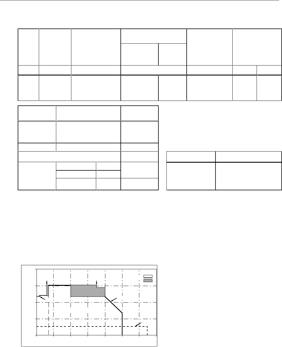
5700A/5720A Series II Calibrator
Service Manual
1-22
Table 1-9. AC Voltage Secondary Performance and Operating Characteristics (continued)
5725A Amplifier:
Stability
±1 °C [Note 1] Temperature Coefficient
Adder Distortion
Bandwidth
Range Frequency 24 Hours 10°-40 °C 0°-10 °C
and
40°-50 °C
Load Regulation
[Note 2]
10 Hz-10 MHz
±(% output)
Hz ±(ppm output + mV) ±(ppm output)/°C
±
(ppm output + mV) 150 pF 1000 pF
1100 V
040 - 1 k
01 k - 20 k
20 k - 50 k
50 k - 100 k
010 + .5
015 + 2
040 + 2
130 + 2
5
5
10
30
5
5
10
30
010 + 1
090 + 6
275 + 11
500 + 30
0.10
0.10
0.30
0.40
0.10
0.15
0.30
0.40
Voltage Range Maximum Current Limits Load Limits Output display formats: Voltage or dBm,
dBm reference 600 Ω.
2.2 V [Note 3]
22 V
220 V
50 mA, 0 °C-40 °C
20 mA, 40 °C-50 °C
>50 Ω,
1000 pF
Minimum output:: 10 % on each range
External sense: Selectable for 2.2 V, 22 V, 220 V, and
1100 V ranges; 5700A/5720A <100 kHz, 5725A <30 kHz
1100 V 6 mA 600 pF Settling time to full accuracy:
5725A Amplifier: 1000 pF [Note 2] Frequency (Hz) Settling time (seconds)
040 Hz-5 kHz 50 mA <20 7
1100 V 05 kHz-30 kHz 70 mA 300 pF 120-120 k 5
30 kHz-100 kHz 70 mA
[Note 4]
150 pF >120 k 2
Notes:
1 Stability specifications are included in Absolute Uncertainty values
for the primary specifications.
2. The 5725A will drive up to 1000 pF of load capacitance.
Uncertainty specifications include loads to 300 pF and 150 pF as
shown under "Load Limits." For capacitances up to the maximum of
1000 pF, add "Load Regulation."
3. 2.2 V Range, 100 kHz-1.2 MHz only: uncertainty specifications
cover loads to 10 mA or 1000 pF. For higher loads, load regulation
is added.
4. Applies from 0 °C to 40 °C
1000
100
10
0
3.5 V
10000
50 Hz10 Hz 1 kHz 100 kHz 1 MHz 30 MHz
Voltage
Frequency
40 Hz 30 Hz 5725A
5700A-03
2.2 x 10
7
V-Hz
15 Hz
5700A/5720A
Volt-Hertz Capability
ahp160f.eps
Figure 1-2. Volt-Hertz Capability
+ 1 second for amplitude or frequency range change;
+ 2 seconds for 5700A/5720A 1100 V range;
+ 4 seconds for 5725A 1100 V range
Overshoot:: <10%
Common mode rejection: 140 dB, DC to 400 Hz
Frequency:
Ranges (Hz):
10.000-119.99
0.1200 k-1.1999 k, 1.200 k-11.999 k
12.00 k-119.99 k,120.0 k-1.1999
Uncertainty: ±0.01 %
Resolution: 11.999 counts
Phase lock: Selectable rear panel BNC input
Phase uncertainty (except 1100 V range):
>30 Hz: ±1° + 0.05°/kHz), <30 Hz: ±3°
Input voltage: 1 V to 10 V rms sine wave (do not exceed
1 V for mV ranges)
Frequency range: 10 Hz to 1.1999 MHz
Lock range: ±2 % of frequency
Lock-in time: Larger of 10/frequency or 10 msec
Phase reference: Selectable, rear panel BNC output
Range: ±180°
Phase Uncertainty (except 1100 V range):
±1° at quadrature points (0°, ±90°, ±180°) elsewhere
±2°
Stability: ±0.1°
Resolution: 1°
Output level: 2.5 V rms ±0.2 V
Frequency range:
50 kHz to 1 kHz, usable 10 Hz to 1.1999 MHz
Introduction and Specifications
Resistance Specifications
1
1-23
1-30. Resistance Specifications
Table 1-10. 5720A Series II Resistance Specifications: 99 % and 95 % Confidence Levels
5720A
99%
99% Confidence Level
Nominal
Value Absolute Uncertainty of Characterized Value
±5 °C from calibration temperature [Note 1] Relative Uncertainty
±1 °C
24 Hours 90 Days 180 Days 1 Year 24 Hours 90 Days
Ω±ppm ±ppm
0
1
1.9
10
19
100
190
1 k
1.9 k
10 k
19 k
100 k
190 k
1 M
1.9 M
10 M
19 M
100 M
50 µΩ
85
85
23
23
10
10
8
8
8
9
9
9
16
17
33
43
100
50 µΩ
95
95
25
25
11
11
9
9
9
9
11
11
18
19
37
47
110
50 µΩ
100
100
26
26
11.5
11.5
9.5
9.5
9.5
9.5
12
12
20
21
40
50
115
50 µΩ
110
110
27
27
12
12
10
10
10
10
13
13
23
24
46
55
120
50 µΩ
32
25
5
4
2
2
2
2
2
2
2
2
2.5
3
10
20
50
50 µΩ
40
33
8
7
4
4
3
3
3
3
3
3
5
6
14
24
60
5720A
95%
95 % Confidence Level
Nominal
Value Absolute Uncertainty of Characterized Value
±5 °C from calibration temperature [Note 1] Relative Uncertainty
±1 °C
24 Hours 90 Days 180 Days 1 Year 24 Hours 90 Days
Ω±ppm ±ppm
0
1
1.9
10
19
100
190
1 k
1.9 k
10 k
19 k
100 k
190 k
1 M
1.9 M
10 M
19 M
100 M
40 µΩ
70
70
20
20
8
8
6.5
6.5
6.5
7.5
7.5
7.5
13
14
27
35
85
40 µΩ
80
80
21
21
9
9
7.5
7.5
7.5
7.5
9
9
15
16
31
39
95
40 µΩ
85
85
22
22
9.5
9.5
8
8
8
8
10
10
17
18
34
42
100
40 µΩ
95
95
23
23
10
10
8.5
8.5
8.5
8.5
11
11
20
21
40
57
100
40 µΩ
27
20
4
3.5
1.6
1.6
1.6
1.6
1.6
1.6
1.6
1.6
2
2.5
8
16
40
40 µΩ
35
26
7
6
3.5
3.5
2.5
2.5
2.5
2.5
2.5
2.5
4
4
12
20
50
Note: 1. Specifications apply to displayed value. 4-wire connections, except 100 MΩ.

5700A/5720A Series II Calibrator
Service Manual
1-24
Table 1-11. 5700A Series II Resistance Specifications: 99 % and 95 % Confidence Levels
5700A
99%
99 % Confidence Level
Nominal
Value Absolute Uncertainty of Characterized Value
±5 °C from calibration temperature [Note 1] Relative Uncertainty
±1 °C
24 Hours 90 Days 180 Days 1 Year 24 Hours 90 Days
Ω±ppm ±ppm
0
1
1.9
10
19
100
190
1 k
1.9 k
10 k
19 k
100 k
190 k
1 M
1.9 M
10 M
19 M
100 M
50 µΩ
85
85
26
24
15
15
11
11
9
9
11
11
16
17
33
43
110
50 µΩ
95
95
28
26
17
17
12
12
11
11
13
13
18
19
37
47
120
50 µΩ
100
100
30
28
18
18
13
13
12
12
14
14
20
21
40
50
125
50 µΩ
110
110
33
31
20
20
15
15
14
14
16
16
23
24
46
55
130
50 µΩ
32
25
5
4
2
2
2
2
2
2
2
2
2.5
3.5
10
20
50
50 µΩ
40
33
8
7
4
4
3.5
3.5
3.5
3.5
3.5
3.5
5
6
14
24
60
5700A
95%
95 % Confidence Level
Nominal
Value Absolute Uncertainty of Characterized Value
±5 °C from calibration temperature [Note 1] Relative Uncertainty
±1 °C
24 Hours 90 Days 180 Days 1 Year 24 Hours 90 Days
Ω±ppm ±ppm
0
1
1.9
10
19
100
190
1 k
1.9 k
10 k
19 k
100 k
190 k
1 M
1.9 M
10 M
19 M
100 M
50 µΩ
70
70
21
20
13
13
9
9
7.5
7.5
9
9
13
14
27
35
90
50 µΩ
80
80
23
22
14
14
10
10
9.5
9.5
11
11
15
16
31
39
100
50 µΩ
85
85
27
24
15
15
11
11
10.5
10.5
12
12
17
18
34
42
105
50 µΩ
95
95
28
27
17
17
13
13
12
12
14
14
20
21
40
47
110
50 µΩ
32
25
5
4
2
2
2
2
2
2
2
2
2.5
3
10
20
50
50 µΩ
40
33
8
7
4
4
3.5
3.5
3.5
3.5
3.5
3.5
5
6
14
24
60
Note: 1. Specifications apply to displayed value. 4-wire connections, except 100 MΩ.
Introduction and Specifications
Resistance Specifications
1
1-25
Table 1-12. Resistance Secondary Performance Specifications and Operating Characteristics
Nominal
Value Stability
±1 °C
[Note 1]
Temperature
Coefficient Adder
[Note 2]
Full Spec
Load Range Maximum
Peak
Current
Maximum
Difference
of
Characterized
Two-Wire Adder
active
compensation
[Note 4]
10°-40 °C 0°-10 °C
and [Note 3] to Nominal
Value Lead Resistance
24 Hours 40°-50 °C 0.1Ω 1Ω
Ω±ppm ±ppm/°C mA mA ±ppm ±mΩ
0
00
8 - 500 500 2 + Im
4 V
µ
4 + Im
4 V
µ
13245
00
8 - 100 700 500 2 + Im
4 V
µ
4 + Im
4 V
µ
1.9 25 6 7
00
8 - 100 500 500 2 + Im
4 V
µ
4 + Im
4 V
µ
10 5 2 3
00
8 - 11 220 300 2 + Im
4 V
µ
4 + Im
4 V
µ
19 4 2 3
00
8 - 11 160 300 2 + Im
4 V
µ
4 + Im
4 V
µ
100 2 2 3
00
8 - 11 70 150 2 + Im
4 V
µ
4 + Im
4 V
µ
190 2 2 3
00
8 - 11 50 150 2 + Im
4 V
µ
4 + Im
4 V
µ
1 k 2 2 3
00
1 - 2 22 150 10 15
1.9 k 2 2 3
00
1 - 1.5 16 150 10 15
10 k 2 2 3 100 - 500 µA 7 150 50 60
19 k 2 2 3
0
50 - 250 µA 5 150 100 120
100 k 2 2 3 10 - 100 µA 1 150 Im= Current
produced by
Ohmmeter
190 k 2 2 3 00 5 - 50 µA 500 µA 150
1 M 2.5 2.5 6 00 5 - 20 µA 100 µA 200
1.9 M 3.5 3 10 02.5 - 10 µA 50 µA 200
10 M 10 5 20 00.5 - 2 µA 10 µA 300
19 M 20 8 40 0.25 - 1 µA5 µA 300
100 M 50 12 100 0 50 - 200 nA 1 µA 500
Notes:
1. Stability specifications are included in the Absolute Uncertainty values in the primary specification tables.
2. Temperature coefficient is an adder to uncertainty specifications that does not apply unless operated
more than 5 °C from calibration temperature, or calibrated outside the range 19 °C to 24 °C. Two
examples:
• Calibrate at 20 °C: Temperature coefficient adder is not required unless operated below 15 °C or
above 25 °C.
• Calibrate at 26 °C: Add 2 °C temperature coefficient adder. Additional temperature coefficient adder is
not required unless operated below 21 °C or above 31 °C.
3. Refer to current derating factors table for loads outside of this range.
4. Active two-wire compensation may be selected for values less than 100 kΩ, with either the front panel or
the meter input terminals as reference plane. Active compensation is limited to 11 mA load, and to 2 V
burden. Two-wire compensation can be used only with Ω-meters that source continuous (not pulsed) dc
current.

5700A/5720A Series II Calibrator
Service Manual
1-26
Table 1-13. Current Derating Factors
Nominal Value Value of Derating Factor K for Over or Under Current
Ω
Two-Wire Comp
I < IL
[Note 1]
Four-Wire
I < IL
[Note 1]
Four-Wire
IU < I < Imax
[Note 2]
SHORT
1
1.9
10
19
100
190
1 k
1.9 k
10 k
19 k
100 k
190 k
1 M
1.9 M
10 M
19 M
100 M
4.4
4.4
4.4
4.4
4.4
4.4
4.4
4.4
4.4
5000
5000
0.3
300
160
30
16
3.5
2.5
0.4
0.4
50
50
7.5
4.0
1.0
0.53
0.2
0.53
0.1
4 x10⁻⁵
1.5 x 10⁻⁴
1.6 x 10⁻³
3 x 10⁻³
1 x 10⁻²
1.9 x 10⁻²
0.1
0.19
2.0
3.8
2 x 10⁻⁵
3.8 x 10⁻⁵
1.5 x 10⁻⁴
2.9 x 10⁻⁴
1 x 10⁻³
1.9 x 10⁻³
Notes:
1. For
I < I L, errors occur due to thermally generated voltages within the 5720A. Use the following
equation to determine the error, and add this error to the corresponding uncertainty or stability
specification.
Error = K(I L - I)/( I L x I)
Where: Error is in mΩ for all two-wire comp values and four-wire short, and in ppm for the remaining
four-wire values.
K is the constant from the above table;
I and IL are expressed in mA for short to 1.9 kΩ;
I and IL are expressed in µA for 10 kΩ to 100 MΩ
2. For
IU < I < IMAX errors occur due to self-heating of the resistors in the calibrator. Use the following
equation to determine the error in ppm and add this error to the corresponding uncertainty or stability
specification.
Error in ppm = K(I2-IU
2)
Where: K is the constant from the above table;
I and IU are expressed in mA for short to 19 kΩ;
I and IU are expressed in µA for 100 kΩ to 100 MΩ
Introduction and Specifications
DC Current Specifications
1
1-27
1-31. DC Current Specifications
Table 1-14. 5720A Series II DC Current Specifications: 99 % and 95 % Confidence Levels
5720A
99%
99 % Confidence Level
Range Resolution Absolute Uncertainty
±5 °C from calibration temperature.
For fields strengths >0.4 V/m but ≤3 V/m,
add 1 % of range.
Relative Uncertainty ±1 °C
24 Hours 90 Days 180 Days 1 Year 24 Hours 90 Days
nA ± (ppm output + nA) ± (ppm output + nA)
220 µA
2.2 mA
22 mA
0.1
1
10
040 + 7
030 + 8
030 + 50
042 + 7
035 + 8
035 + 50
045 + 7
037 + 8
037 + 50
050 + 7
040 + 8
040 + 50
024 + 7
024 + 8
024 + 50
026 + 7
026 + 8
026 + 50
µA± (ppm output + µA) ± (ppm output + µA)
220 mA
2.2 A
[Note 1]
0.1
1
040 + 0.8
060 + 15
045 + 0.8
070 + 15
047 + 0.8
080 + 15
050 + 0.8
090 + 15
026 + 0.5
040 + 12
030 + 0.5
045 + 12
5725A Amplifier:
11 A 10 330 + 470 340 + 480 350 + 480 360 + 480 100 + 130 110 + 130
5720A
95%
95 % Confidence Level
Range Resolution Absolute Uncertainty
±5 °C from calibration temperature
For fields strengths >0.4 V/m but ≤3 V/m,
add 1 % of range.
Relative Uncertainty ±1 °C
24 Hours 90 Days 180 Days 1 Year 24 Hours 90 Days
nA ± (ppm output + nA) ± (ppm output + nA)
220 µA
2.2 mA
22 mA
0.1
1
10
032 + 6
025 + 7
025 + 40
035 + 6
030 + 7
030 + 40
037 + 6
033 + 7
033 + 40
040 + 6
035 + 7
035 + 40
020 + 6
020 + 7
020 + 40
022 + 6
022 + 7
022 + 40
µA± (ppm output + µA) ± (ppm output + µA)
220 mA
2.2 A
[Note 1]
0.1
1
035 + 0.7
050 + 12
040 + 0.7
060 + 12
042 + 0.7
070 + 12
045 + 0.7
080 + 12
020 + 0.7
032 + 12
025 + 0.7
040 + 12
5725A Amplifier:
11 A 10 330 + 470 340 + 480 350 + 480 360 + 480 100 + 130 110 + 130
Note: Maximum output from calibrator terminals is 2.2 A. Uncertainty specifications for 220 mA and 2.2 mA
ranges are increased by a factor of 1.3 when supplied through 5725A terminals.
Specifications are otherwise identical for all output locations.
1. Add to uncertainty specifications:
±200 x I2 ppm for >100 mA on 220 mA range
±10 x I2 ppm for >1 A on 2.2 A range
5700A/5720A Series II Calibrator
Service Manual
1-28
Table 1-15. 5700A Series II DC Current Specifications: 99 % and 95 % Confidence Levels
5700A
99%
99 % Confidence Level
Range Resolution
Absolute Uncertainty
±5 °C from calibration temperature
For fields strengths >0.4 V/m but ≤3 V/m,
add 1% of range.
Relative Uncertainty ±1 °C
24 Hours 90 Days 180 Days 1 Year 24 Hours 90 Days
nA ± (ppm output + nA) ± (ppm output + nA)
220 µA
2.2 mA
22 mA
0.1
1
10
045 + 10
045 + 10
045 + 100
050 + 10
050 + 10
050 + 100
055 + 10
055 + 10
055 + 100
060 + 10
060 + 10
060 + 100
024 + 2
024 + 5
024 + 50
026 + 2
026 + 5
026 + 50
µA± (ppm output + µA) ± (ppm output + µA)
220 mA
2.2 A
[Note 1]
0.1
1
055 + 1
075 + 30
060 + 1
080 + 30
065 + 1
090 + 30
070 + 1
095 + 30
026 + .3
040 + 7
030 + .3
045 + 7
5725A Amplifier:
11 A 10 330 + 470 340 + 480 350 + 480 360 + 480 100 + 130 110 + 130
5700A
95%
95 % Confidence Level
Range Resolution
Absolute Uncertainty
±5 °C from calibration temperature
For fields strengths >0.4 V/m but ≤3 V/m,
add 1 % of range.
Relative Uncertainty ±1 °C
24 Hours 90 Days 180 Days 1 Year 24 Hours 90 Days
nA ± (ppm output + nA) ± (ppm output + nA)
220 µA
2.2 mA
22 mA
0.1
1
10
035 + 8
035 + 8
035 + 80
040 + 8
040 + 8
040 + 80
045 + 8
045 + 8
045 + 80
050 + 8
050 + 8
050 + 80
020 + 1.6
020 + 4
020 + 80
022 + 1.6
022 + 4
022 + 80
µA± (ppm output + µA) ± (ppm output + µA)
220 mA
2.2 A
[Note 1]
0.1
1
045 + 0.8
060 + 25
050 + 0.8
065 + 25
055 + 0.8
075 + 25
060 + 0.8
080 + 25
022 + 0.25
035 + 6
025 + 0.25
040 + 6
5725A Amplifier:
11 A 10 330 + 470 340 + 480 350 + 480 360 + 480 100 + 130 110 + 130
Note: Maximum output from the calibrator’s terminals is 2.2 A. Uncertainty specifications for 220 mA and
2.2 mA ranges are increased by a factor of 1.3 when supplied through 5725A terminals.
Specifications are otherwise identical for all output locations.
1. Add to uncertainty specifications:
±200 x I2 ppm for >100 mA on 220 mA range
±10 x I2 ppm for >1A on 2.2A range
Introduction and Specifications
DC Current Specifications
1
1-29
Table 1-16. DC Current Secondary Performance Specifications and Operating Characteristics
Temperature
Coefficient [Note 2] Noise
Range Stability
±1 °C [Note 1] 10 °-40 °C 0 °-10 °C
and
Compliance
Limits
Burden
Voltage
Adder
[Note 3]
Maximum
Load for
Full
Accuracy
Bandwidth
0.1-10 Hz Bandwidth
1
0 Hz-10 kHz
24 Hours 40 °-50 °C [Note 4] pk-pk RMS
± (ppm output
+ nA) ± (ppm output + nA)/ °C ±nA/V Ωppm output
+ nA nA
220 µA
2.2 mA
22 mA
220 mA
2.2 A
05 + 1
05 + 5
05 + 50
08 + 300
09 + 7 µA
0
1 + 0.40
0
1 + 2
0
1 + 20
0
1 + 200
0
1 + 2.5 µΑ
0
3 + 1
0
3 + 10
0
3 + 100
0
3 + 1 µA
0
3 + 10 µA
10
10
10
10
3 [Note 5]
0.2
0.2
10
100
2 µA
20k
2k
200
20
2
06 + .9
06 + 5
06 + 50
09 + 300
12 + 1.5 µA
10
10
50
500
20 µA
5725A ± (ppm output
+ µA) ± (ppm output + µA)/
°C ppm output
+ µAµA
11 A 25 + 100 20 + 75 30 + 120 4
0
4 15 + 70 175
Notes:
Maximum output from the calibrator’s terminals is 2.2 A. Uncertainty specifications for 220 mA and 2.2 mA
ranges are increased by a factor of 1.3 when supplied through 5725A terminals.
1. Stability specifications are included in the Absolute Uncertainty values for the primary specifications.
2. Temperature coefficient is an adder to uncertainty specifications. It does not apply unless operating more
than ±5 °C from calibration temperature.
3. Burden voltage adder is an adder to uncertainty specifications that does not apply unless burden voltage is
greater than 0.5 V.
4. For higher loads, multiply uncertainty specification by: 10.1 x actual load
maximum load for full accuracy
+
5. The calibrator’s compliance limit is 2 V for outputs from 1 A to 2.2 A. 5725A Amplifier may be used in range-
lock mode down to 0 A.
Minimum output: 0 for all ranges, including 5725A.
Settling time to full accuracy: 1 second for mA and mA ranges; 3 seconds for 2.2 A range; 6 seconds for 11 A
range; + 1 second for range or polarity change
Overshoot: <5 %

5700A/5720A Series II Calibrator
Service Manual
1-30
1-32. AC Current Specifications
Table 1-17. 5720A Series II AC Current Specifications: 99 % Confidence Level
5720A
99%
99 % Confidence Level
Range Resolution Frequency Absolute Uncertainty
±5 °C from calibration temperature
For fields strengths >0.4 V/m but ≤3 V/m,
add 1 % of range.
Relative Uncertainty
±1 °C
24 Hours 90 Days 180 Days 1 Year 24 Hours 90 Days
Hz ± (ppm output + nA) ± (ppm output + nA)
220 µA1 nA
010 - 20
020 - 40
040 - 1 k
01k - 5 k
05k - 10 k
0260 + 20
0170 + 12
0120 + 10
0300 + 15
1000 + 80
0280 + 20
0180 + 12
0130 + 10
0320 + 15
1100 + 80
0290 + 20
0190 + 12
0135 + 10
0340 + 15
1200 + 80
0300 + 20
0200 + 12
0140 + 10
0350 + 15
1300 + 80
0260 + 20
0130 + 12
0100 + 10
0250 + 15
0900 + 80
0280 + 20
0150 + 12
0110 + 10
0280 + 15
01000 + 80
2.2 mA 10 nA
010 - 20
020 - 40
040 - 1 k
01k - 5 k
05k - 10 k
0260 + 50
0170 + 40
0120 + 40
0210 + 130
1000 + 800
0280 + 50
0180 + 40
0130 + 40
0220 + 130
1100 + 800
0290 + 50
0190 + 40
0135 + 40
0230 + 130
1200 + 800
0300 + 50
0200 + 40
0140 + 40
0240 + 130
1300 + 800
0260 + 50
0130 + 40
0100 + 40
0250 + 130
0900 + 800
0280 + 50
0150 + 40
0110 + 40
0280 + 130
1000 + 800
22 mA 100 nA
010 - 20
020 - 40
040 - 1 k
01k - 5 k
05k - 10 k
0260 + 500
0170 + 400
0120 + 400
0210 + 700
1000 + 6000
0280 + 500
0180 + 400
0130 + 400
0220 + 700
1100 + 6000
0290 + 500
0190 + 400
0135 + 400
0230 + 700
1200 + 6000
0300 + 500
0200 + 400
0140 + 400
0240 + 700
1300 + 6000
0260 + 500
0130 + 400
0100 + 400
0250 + 700
0900 + 6000
0280 + 500
0150 + 400
0110 + 400
0280 + 700
1000 + 6000
Hz ± (ppm output + µA) ± (ppm output + µA)
220 mA 1 µA
010 - 20
020 - 40
040 - 1 k
01k - 5 k
05k - 10 k
0260 + 5
0170 + 4
0120 + 3
0210 + 4
1000 + 12
0280 + 5
0180 + 4
0130 + 3
0220 + 4
1100 + 12
0290 + 5
0190 + 4
0135 + 3
0230 + 4
1200 + 12
0300 + 5
0200 + 4
0140 + 3
0240 + 4
1300 + 12
0260 + 5
0130 + 4
0100 + 3
0250 + 4
0900 + 12
0280 + 5
0150 + 4
0110 + 3
0280 + 4
1000 + 12
2.2 A 10 µA020 - 1 k
01 k - 5 k
05 k - 10 k
0290 + 40
0440 + 100
6000 + 200
0300 + 40
0460 + 100
7000 + 200
0310 + 40
0480 + 100
7500 + 200
0320 + 40
0500 + 100
8000 + 200
0300 + 40
0500 + 100
6000 + 200
0350 + 40
0520 + 100
7000 + 200
5725A Amplifier:
11 A 100 µA040 - 1 k
01 k - 5 k
05 k - 10 k
0370 + 170
0800 + 380
3000 + 750
0400 + 170
0850 + 380
3300 + 750
0440 + 170
0900 + 380
3500 + 750
0460 + 170
0950 + 380
3600 + 750
0300 + 170
0700 + 380
2800 + 750
0330 + 170
0800 + 380
3200 + 750
Note: Maximum output from the calibrator’s terminals is 2.2 A. Uncertainty specifications for 220 µA and 2.2 mA
ranges are increased by a factor of 1.3 plus 2 µA when supplied through 5725A terminals. Specifications are
otherwise identical for all output locations.
Introduction and Specifications
AC Current Specifications
1
1-31
Table 1-18. 5720A Series II AC Current Specifications: 95 % Confidence Level
5720A
95%
95 % Confidence Level
Range Resolution Frequency Absolute Uncertainty
±5 °C from calibration temperature
For fields strengths >0.4 V/m but ≤3 V/m,
add 1 % of range.
Relative Uncertainty
±1 °C
24 Hours 90 Days 180 Days 1 Year 24 Hours 90 Days
Hz ± (ppm output + nA) ± (ppm output + nA)
220 µA1 nA
010 - 20
020 - 40
040 - 1 k
01k - 5 k
05k - 10 k
0210 + 16
0130 + 10
0100 + 8
0240 + 12
0800 + 65
0230 + 16
0140 + 10
0110 + 8
0250 + 12
0900 + 65
0240 + 16
0150 + 10
0115 + 8
0270 + 12
1000 + 65
0250 + 16
0160 + 10
0120 + 8
0280 + 12
1100 + 65
0210 + 16
0110 + 10
0080 + 8
0200 + 12
0700 + 65
0230 + 16
0130 + 10
0090 + 8
0230 + 12
0800 + 65
2.2 mA 10 nA
010 - 20
020 - 40
040 - 1 k
01k - 5 k
05k - 10 k
0210 + 40
0140 + 35
0100 + 35
0170 + 110
0800 + 650
0230 + 40
0140 + 35
0110 + 35
0180 + 110
0900 + 650
0240 + 40
0150 + 35
0115 + 35
0190 + 110
1000 + 650
0250 + 40
0160 + 35
0120 + 35
0200 + 110
1100 + 650
0210 + 40
0110 + 35
0080 + 35
0200 + 110
0700 + 650
0230 + 40
0130 + 35
0090 + 35
0230 + 110
0800 + 650
22 mA 100 nA
010 - 20
020 - 40
040 - 1 k
01k - 5 k
05k - 10 k
0210 + 400
0130 + 350
0100 + 350
0170 + 550
0800 + 5000
0230 + 400
0140 + 350
0110 + 350
0180 + 550
0900 + 5000
0240 + 400
0150 + 350
0115 + 350
0190 + 550
1000 + 5000
0250 + 400
0160 + 350
0120 + 350
0200 + 550
1100 + 5000
0210 + 400
0110 + 350
0080 + 350
0200 + 550
0700 + 5000
0230 + 400
0130 + 350
0090 + 350
0230 + 550
0800 + 5000
Hz ± (ppm output + µA) ± (ppm output + µA)
220 mA 1 µA
010 - 20
020 - 40
040 - 1 k
01k - 5 k
05k - 10 k
0210 + 4
0130 + 3.5
0100 + 2.5
0170 + 3.5
0800 + 10
0230 + 4
0140 + 3.5
0110 + 2.5
0180 + 3.5
0900 + 10
0240 + 4
0150 + 3.5
0115 + 2.5
0190 + 3.5
1000 + 10
0250 + 4
0160 + 3.5
0120 + 2.5
0200 + 3.5
1100 + 10
0210 + 4
0110 + 3.5
0080 + 2.5
0200 + 3.5
0700 + 10
0230 + 4
0130 + 3.5
090 + 2.5
0230 + 3.5
0800 + 10
2.2 A 10 µA020 - 1 k
01 k - 5 k
05 k - 10 k
0230 + 35
0350 + 80
5000 + 160
0240 + 35
0390 + 80
6000 + 160
0250 + 35
0420 + 80
6500 + 160
0260 + 35
0450 + 80
7000 + 160
0250 + 35
0400 + 80
5000 + 160
0300 + 35
0440 + 80
6000 + 160
5725A Amplifier:
11 A 100 µA040 - 1 k
01 k - 5 k
05 k - 10 k
0370 + 170
0800 + 380
3000 + 750
0400 + 170
0850 + 380
3300 + 750
0440 + 170
0900 + 380
3500 + 750
0460 + 170
0950 + 380
3600 + 750
0300 + 170
0700 + 380
2800 + 750
0330 + 170
0800 + 380
3200 + 750
Note: Maximum output from the calibrator’s terminals is 2.2 A. Uncertainty specifications for 220 µA and
2.2 mA ranges are increased by 1.3 x plus 2 µA when supplied through 5725A terminals. Specifications are
otherwise identical for all output locations.

5700A/5720A Series II Calibrator
Service Manual
1-32
Table 1-19. 5700A Series II AC Current Specifications: 99 % Confidence Level
5700A
99%
99 % Confidence Level
Range Resolution Frequency Absolute Uncertainty
±5 °C from calibration temperature
For fields strengths >0.4 V/m but ≤3 V/m,
add 1 % of range.
Relative Uncertainty
±1 °C
24 Hours 90 Days 180 Days 1 Year 24 Hours 90 Days
Hz ± (ppm output + nA) ± (ppm output + nA)
220 µA1 nA
010 - 20
020 - 40
040 - 1 k
01k - 5 k
0
5k - 10 k
0650 + 30
0350 + 25
0120 + 20
0500 + 50
1500 + 100
0700 + 30
0380 + 25
0140 + 20
0600 + 50
1600 + 100
0750 + 30
0410 + 25
0150 + 20
0650 + 50
1700 + 100
00 800 + 30
00 420 + 25
00 160 + 20
00 700 + 50
0 1800 + 100
0450 + 30
0270 + 25
0110 + 20
0450 + 50
1400 + 100
0500 + 30
0300 + 25
0120 + 20
0500 + 50
1500 + 100
2.2 mA 10 nA
010 - 20
020 - 40
040 - 1 k
01k - 5 k
0
5k - 10 k
0650 + 50
0350 + 40
0120 + 40
0500 + 500
1500 + 1000
0700 + 50
0380 + 40
0140 + 40
0600 + 500
1600 + 1000
0750 + 50
0410 + 40
0150 + 40
0650 + 500
1700 + 1000
00 800 + 50
0 0420 + 40
00 160 + 40
00 700 + 500
0 1800 + 1000
0450 + 50
0270 + 40
0110 + 40
0450 + 500
1400 + 1000
0500 + 50
0300 + 40
0120 + 40
0500 + 500
1500 + 1000
22 mA 100 nA
010 - 20
020 - 40
040 - 1 k
01k - 5 k
0
5k - 10 k
0650 + 500
0350 + 400
0120 + 400
0500 + 5000
1500 + 10,000
0700 + 500
0380 + 400
0140 + 400
0600 + 5000
1600 + 10,000
0750 + 500
0410 + 400
0150 + 400
0650 + 5000
1700 + 10,000
00 800 + 500
00 420 + 400
00 160 + 400
00 700 + 5000
0 1800 + 10,000
0450 + 500
0270 + 400
0110 + 400
0450 + 5000
1400 + 10,000
0500 + 500
0300 + 400
0120 + 400
0500 + 5000
1500 +
10,000
Hz ± (ppm output + µA) ± (ppm output + µA)
220 mA 1 µA
010 - 20
020 - 40
040 - 1 k
01k - 5 k
0
5k - 10 k
0650 + 5
0350 + 4
0120 + 4
0500 + 50
1500 + 100
0700 + 5
0380 + 4
0150 + 4
0600 + 50
1600 + 100
0750 + 5
0410 + 4
0170 + 4
0650 + 50
1700 + 100
00 800 + 5
00 420 + 4
00 180 + 4
0 700 + 50
0 1800 + 100
0450 + 5
0280 + 4
0110 + 4
0450 + 50
1400 + 100
0500 + 5
0300 + 4
0130 + 4
0500 + 50
1500 + 100
2.2 A 10 µA
0
20 - 1 k
0
1 k - 5 k
0
5 k - 10 k
0600 + 40
0700 + 100
8000 + 200
0650 + 40
0750 + 100
9000 + 200
0700 + 40
0800 + 100
9500 + 200
0 750 + 40
00 850 + 100
10,000 + 200
0600 + 40
0650 + 100
7500 + 200
0650 + 40
0750 + 100
8500 + 200
5725A Amplifier:
11 A 100 µA
0
40 - 1 k
0
1 k - 5 k
0
5 k - 10 k
0370 + 170
0800 + 380
3000 + 750
400 + 170
850 + 380
3300 + 750
0440 + 170
0900 + 380
3500 + 750
00 460 + 170
00 950 + 380
0 3600 + 750
0300 + 170
0700 + 380
2800 + 750
0330 + 170
0800 + 380
3200 + 750
Note: Maximum output from the calibrator’s terminals is 2.2 A. Uncertainty specifications for 220 µA and 2.2 mA
ranges are increased by 1.3 x plus 2 µA when supplied through 5725A terminals. Specifications are otherwise
identical for all output locations.

Introduction and Specifications
AC Current Specifications
1
1-33
Table 1-20. 5700A Series II AC Current Specifications: 95 % Confidence Level
5700A
95%
95 % Confidence Level
Range Resolution Frequency Absolute Uncertainty
±5 °C from calibration temperature
For fields strengths >0.4 V/m but ≤3 V/m,
add 1 % of range.
Relative Uncertainty
±1 °C
24 Hours 90 Days 180 Days 1 Year 24 Hours 90 Days
Hz ± (ppm output + nA) ± (ppm output + nA)
220 µA1 nA
010 - 20
020 - 40
040 - 1 k
01k - 5 k
0
5k - 10 k
0550 + 25
0280 + 20
0100 + 16
0400 + 40
1300 + 80
0600 + 25
0310 + 20
0120 + 16
0500 + 40
1400 + 80
0650 + 25
0330 + 20
0130 + 16
0550 + 40
1500 + 80
0700 + 25
0350 + 20
0140 + 16
0600 + 40
1600 + 80
0375 + 25
0220 + 20
090 + 16
0375 + 40
1200 + 80
0400 + 25
0250 + 20
0100 + 16
0400 + 40
1200 +80
2.2 mA 10 nA
010 - 20
020 - 40
040 - 1 k
01k - 5 k
0
5k - 10 k
0550 + 40
0280 + 35
0100 + 35
0400 + 400
1300 + 800
0600 + 40
0310 + 35
0120 + 35
0500 + 400
1400 + 800
0650 + 40
0330 + 35
0130 + 35
0550 + 400
1500 + 800
0700 + 40
0350 + 35
0140 + 35
0600 + 400
1600 + 800
0375 + 40
0220 + 35
0090 + 35
0375 + 400
1200 + 800
0400 + 40
0250 + 35
0100 + 35
0400 + 400
1200 + 800
22 mA 100 nA
010 - 20
020 - 40
040 - 1 k
01k - 5 k
0
5k - 10 k
0550 + 400
0280 + 350
0100 + 350
0400 + 4000
1300 + 8000
0600 + 400
0310 + 350
0120 + 350
0500 + 4000
1400 + 8000
0650 + 400
0330 + 350
0130 + 350
0550 + 4000
1500 + 8000
0700 + 400
0350 + 350
0140 + 350
0600 + 4000
1600 + 8000
0375 + 400
0220 + 350
0090 + 350
0375 + 4000
1200 + 8000
0400 + 400
0250 + 350
0100 + 350
0400 + 4000
1200 + 8000
Hz ± (ppm output + µA) ± (ppm output + µA)
220 mA 1 µA
010 - 20
020 - 40
040 - 1 k
01k - 5 k
0
5k - 10 k
0550 + 4
0280 + 3.5
0100 + 3.5
0400 + 40
1300 + 80
0600 + 4
0310 + 3.5
0120 + 3.5
0500 + 40
1400 + 80
0650 + 4
0330 + 3.5
0130 + 3.5
0550 + 40
1500 + 80
0700 + 4
0350 + 3.5
0140 + 3.5
0600 + 40
1600 + 80
0375 + 4
0220 + 3.5
0090 + 3.5
0375 + 40
1200 + 80
0400 + 4
0250 + 3.5
0100 + 3.5
0400 + 40
1200 + 80
2.2 A 10 µA
0
20 - 1 k
0
1 k - 5 k
0
5 k - 10 k
0500 + 35
0600 + 80
6500 + 160
0550 + 35
0650 + 80
7500 + 160
0600 + 35
0700 + 80
8000 + 1600
0650 + 35
0750 + 80
8500 + 160
0500 + 35
0550 + 80
6000 + 160
0550 + 35
0650 + 80
7000 + 160
5725A Amplifier:
11 A 100 µA
0
40 - 1 k
0
1 k - 5 k
0
5 k - 10 k
0370 + 170
0800 + 380
3000 + 750
0400 + 170
0850 + 380
3300 + 750
0440 + 170
0900 + 380
3500 + 750
0460 + 170
0950 + 380
3600 + 750
0300 + 170
0700 + 380
2800 + 750
0330 + 170
0800 + 380
3200 + 750
Note: Maximum output from the calibrator’s terminals is 2.2 A. Uncertainty specifications for 220 µA and
2.2 mA ranges are increased by a factor of 1.3 plus 2 µA when supplied through 5725A terminals.
Specifications are otherwise identical for all output locations.

5700A/5720A Series II Calibrator
Service Manual
1-34
Table 1-21. AC Current Secondary Performance Specifications and Operating Characteristics
Stability
±1 °C [Note 1] Temperature Coefficient
[Note 2] Compliance
Limits Maximum
Resistive
Load
Noise and
Distortion
Range Frequency 24 Hours 10°-40 °C 0°-10 °C and
40°-50 °C For Full
Accuracy
[Note 3]
Bandwidth
10 Hz-50 kHz
<0.5V Burden
Hz ± (ppm output + nA) ± (ppm output + nA)/°C V rms Ω± (% output + µA)
220 µA010 - 20
020 - 40
040 - 1 k
01k - 5 k
05k - 10 k
150 + 5
080 + 5
030 + 3
050 + 20
400 + 100
050 + 5
020 + 5
004 + 0.5
010 + 1
020 + 100
050 + 5
020 + 5
010 + 0.5
020 + 1
020 + 100
72k
[Note 6]
0.05 + 0.1
0.05 + 0.1
0.05 + 0.1
0.25 + 0.5
00.5 + 1
2.2 mA 010 - 20
020 - 40
040 - 1 k
01k - 5 k
05k - 10 k
150 + 5
080 + 5
030 + 3
050 + 20
400 + 100
050 + 5
020 + 4
004 + 1
010 + 100
050 + 400
050 + 5
020 + 4
010 + 2
020 + 100
050 + 400
7 500 0.05 + 0.1
0.05 + 0.1
0.05 + 0.1
0.25 + 0.5
00.5 + 1
22 mA 010 - 20
020 - 40
040 - 1 k
01k - 5 k
05k - 10 k
150 + 50
080 + 50
030 + 30
050 + 500
400 + 1000
050 + 10
020 + 10
004 + 10
010 + 500
050 + 1000
050 + 10
020 + 10
010 + 20
020 + 400
050 + 1000
7 150 0.05 + 0.1
0.05 + 0.1
0.05 + 0.1
0.25 + 0.5
00.5 + 1
Hz ± (ppmutput + µA) ± (ppm output + µA)/°C
220 mA 010 - 20
020 - 40
040 - 1 k
01k - 5 k
05k - 10 k
150 + 0.5
080 + 0.5
030 + 0.3
050 + 3
400 + 5
050 + 0.05
020 + 0.05
004 + 0.1
010 + 2
050 + 5
050 + 0.05
020 + 0.05
010 + 0.1
020 + 2
050 + 5
7 15 0.05 + 10
0.05 + 10
0.05 + 10
0.25 + 50
00.5 + 100
2.2 A 20 - 1 k
1 k - 5 k
5 k - 10 k
050 + 5
080 + 20
800 + 50
004 + 1
010 + 5
050 + 10
010 + 1
020 + 5
050 + 10
1.4
[Note 4]
0.5 0.5 + 100
0.3 + 500
0 1 + 1 mA
5725A Amplifier: ± (% output)
11 A 40 - 1 k
1 k - 5 k
5 k - 10 k
075 + 100
100 + 150
200 + 300
020 + 75
040 + 75
100 + 75
030 + 75
050 + 75
100 + 75
3 3 0.05
0.12
0.5
[Note 5]
Notes:
Maximum output from 5720A terminals is 2.2 A. Uncertainty specifications for 220 µA and 2.2 mA ranges are increased by a
factor of 1.3, plus 2 µA when supplied through 5725A terminals. Specifications are otherwise identical for all output locations.
1. Stability specifications are included in the Absolute Uncertainty values for the primary specifications.
2. Temperature coefficient is an adder to uncertainty specifications that does not apply unless operating more than ±5 °C from
calibration temperature.
3. For larger resistive loads multiply uncertainty specifications by: (actual load
maximum load for full accuracy )2
4. 1.5 V compliance limit above 1 A. 5725A Amplifier may be used in range-lock mode down to 1 A.
5. For resistive loads within rated compliance voltage limits.
6. For outputs from the Aux Current terminals, the maximum resistive load for full accuracy is 1 kΩ. For larger resistive loads,
multiply the uncertainty as described in Note 3.
Minimum output: 9 µA for 220 µA range, 10 % on all other ranges. 1 A minimum for 5725A.
Inductive load limits: 400 µH (5700A/5720A, or 5725A). 20 µH for 5700A/5720A output >1 A.
Power factors: 5700A/5720A, 0.9 to 1; 5725A, 0.1 to 1. Subject to compliance voltage limits.
Frequency:
Range (Hz): 10.000-11.999, 12.00-119.99, 120.0-1199.9, 1.200 k-10.000 k
Uncertainty: ±0.01 %
Resolution: 11,999 counts
Settling time to full accuracy: 5 seconds for 5700A/5720A ranges; 6 seconds for 5725A 11 A range; +1 second for amplitude
or frequency range change.
Overshoot: <10 %
Introduction and Specifications
Wideband AC Voltage (Option 5700-03) Specifications
1
1-35
1-33. Wideband AC Voltage (Option 5700-03) Specifications
Table 1-22. Wideband AC Voltage (Option 5700-03) Specifications
Specifications apply to the end of the cable and 50 Ω termination used for calibration
Range Resolution Absolute Uncertainty
±5 °C from calibration temperature
30 Hz-500 kHz
Volts dBm 24 Hours 90 Days 180 Days 1 Year
± (% output + µV)
1.1 mV -46 10 nV 0.4 + 0.4 00.5 + 0.4 00.6 + 0.4 0.8 + 2
3 mV -37 10 nV 0.4 + 1 0.45 + 1 00.5 + 1 0.7 + 3
11 mV -26 100 nV 0.2 + 4 0.35 + 4 00.5 + 4 0.7 + 8
33 mV -17 100 nV 0.2 + 10 00.3 + 10 0.45 + 10 0.6 + 16
110 mV -6.2 1 µV 0.2 + 40 00.3 + 40 0.45 + 40 0.6 + 40
330 mV +3.4 1 µV 0.2 + 100 0 2.5 + 100 0.35 + 100 0.5 + 100
1.1 V +14 10 µV 0.2 + 400 0.25 + 400 0.35 + 400 0.5 + 400
3.5 V +24 10 µV 0.15 + 500 00.2 + 500 00.3 + 500 0.4 + 500
Frequency Frequency
Resolution Amplitude Flatness, 1 kHz Reference
Voltage Range Temperature
Coefficient
Settling
Time To
Full
Accuracy
Harmonic
Distortion
1.1 mV 3 mV >3 mV
Hz Hz ± (% output + floor indicated) ±ppm/°C Seconds dB
00 10 - 30 0.01 0.3 0.3 0.3 100 7 -40
00 30 - 120 0.01 0.1 0.1 0.1 100 7 -40
0 120 - 1.2 k 0.1 0.1 0.1 0.1 100 5 -40
01.2 k - 12 k 1 0.1 0.1 0.1 100 5 -40
0 12 k - 120 k 10 0.1 0.1 0.1 100 5 -40
120 k - 1.2 M 100 00.2 + 3 µV00.1 + 3 µV 0.1 + 3 µV 100 5 -40
1.2 M - 2 M 100 k 00.2 + 3 µV00.1 + 3 µV 0.1 + 3 µV 100 0.5 -40
0 2 M - 10 M 100 k 00.4 + 3 µV00.3 + 3 µV 0.2 + 3 µV 100 0.5 -40
10 M - 20 M 1 M 00.6 + 3 µV00.5 + 3 µV 0.4 + 3 µV 150 0.5 -34
20 M - 30 M 1 M 10.5 + 15 µV 10.5 + 3 µV0 1 + 3 µV 300 0.5 -34
Additional Operating Information:
dBm reference = 50 Ω
Range boundaries are at voltage points, dBm levels are approximate.
dBm = 10 log (Power
1 mW ) ; 0.22361 V across 50 Ω = 1 mW or 0 dBm
Minimum output: 300 µV (-57 dBm)
Frequency uncertainty: ±0.01 %
Frequency resolution: 11,999 counts to 1.1999 MHz, 119 counts to 30 MHz.
Overload protection: A short circuit on the wideband output will not result in damage. After settling time, normal operation is
restored upon removal.
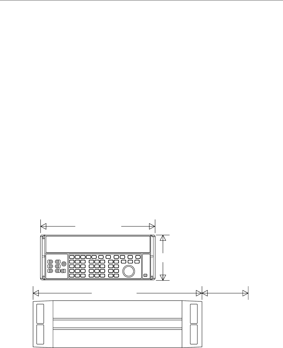
5700A/5720A Series II Calibrator
Service Manual
1-36
1-34. General Specifications
Warm-Up Time: Twice the time since last warmed up, to a maximum of 30 minutes.
System installation: Rear output configuration and rack- mount kit available.
Standard interfaces: IEEE-488, RS-232, 5725A, 5205A or 5215A, 5220A, phase lock in (BNC), phase
reference out (BNC).
Temperature performance: Operating: 0 °C to 50 °C. Calibration: 15 °C to 35 °C. Storage: -40 °C to
75 °C; DC Zeros calibration required every 30 days.
Relative humidity: Operating: <80 % to 30 °C, <70 % to 40 °C, <40 % to 50 °C. Storage: <95 %, non-
condensing. A power stabilization period of four days may be required after extended storage at high
temperature and humidity.
Safety: Designed to comply with UL3111; EN61010; CSA C22.2 No. 1010; ANSI/ISA S82.01-1994
Guard isolation: 20 V
EMI/RFI: Designed to comply with FCC Rules Part 15, Subpart B, Class B; EN50081-1, EN50082-1
Electro Static Discharge: This instrument meets criteria C for ESD requirements per EN61326
Line Power: 47 to 63 Hz; ±10 % allowed about selectable nominal line voltage: 100 V, 110 V, 115 V,
120 V, 200 V, 220 V, 230 V, 240 V. Maximum power: 5700A/5720A, 300 VA; 5725A, 750 VA.
Size:
5700A/5720A: Height 17.8 cm (7 in), standard rack increment, plus 1.5 cm (0.6 in) for feet; Width 43.2 cm
(17 in), standard rack width; Depth 63.0 cm (24.8 in), overall; 57.8 cm (22.7 in), rack depth.
5725A: Height 13.3 cm, (5.25 in); Width and depth same as 5700A/5720A. Both units project 5.1 cm, (2 in)
from rack front.
Weight: 5700A/5720A: 27kg (62 lbs); 5725A: 32kg (70 lbs).
43.2 cm (17 in)
17.8 cm (7 in)
63 cm (24.8 in) 6.35 cm (2.5 in)
FOR CABLE
ACCESS

Introduction and Specifications
Auxiliary Amplifier Specifications
1
1-37
1-35. Auxiliary Amplifier Specifications
For complete specifications, see the 5205A and 5220A Operators Manuals.
5205A (220V - 1100 V ac, 0 V - 1100 V dc)
Overshoot: < 10 %
Distortion (bandwidth 10 Hz - 1 MHz):
10 Hz - 20 kHz
20 kHz - 50 kHz
50 kHz - 100 kHz
0.07 %
0.2 %
0.25 %
Frequency
(Hz)
90 Day Accuracy
at 23° ±5 °C
± (% output + % range)
Temperature Coefficient for
0°-18 °C and 28°-50 °C
± (ppm output + ppm range)/ °C
00 dc
010 - 40
040 - 20 k
20 k - 50 k
50 k - 100 k
0.05 + 0.005
0.15 + 0.005
0.04 + 0.004
0.08 + 0.006
00.1 + 0.01
15 + 3
45 + 3
15 + 3
50 + 10
70 + 20
5220A (AC Current, 180-day specifications):
Accuracy:
20 Hz - 1 kHz
1 kHz - 5 kHz
0.07% + 1 mA
(0.07% + 1mA) x frequency in kHz
Temperature Coefficient (0° - 18 °C and 28° - 50 °C): (0.003 % + 100 µA)/°C
Distortion (bandwidth 300 kHz):
20 Hz - 1 kHz
1 kHz - 5 kHz
0.1% + 1 mA
(0.1% + 1 mA) x frequency in kHz
Note: 5700A/5720A combined with 5220A is not specified for inductive loads.

5700A/5720A Series II Calibrator
Service Manual
1-38
2-1
Chapter 2
Theory of Operation
Title Page
2-1. Introduction .......................................................................................... 2-5
2-2. Calibrator Overview............................................................................. 2-5
2-3. Internal References .......................................................................... 2-5
2-4. Hybrid Reference Amplifiers ...................................................... 2-5
2-5. Fluke Thermal Sensor (FTS)....................................................... 2-5
2-6. Digital-to-Analog Converter (DAC)............................................ 2-6
2-7. Digital Section Overview ..................................................................... 2-6
2-8. Analog Section Overview..................................................................... 2-6
2-9. Functional Description Presented by Output Function........................ 2-8
2-10. DC Voltage Functional Description................................................. 2-8
2-11. AC Voltage Functional Description................................................. 2-11
2-12. Wideband AC V Functional Description (Option -03).................... 2-12
2-13. DC Current Functional Description................................................. 2-12
2-14. AC Current Functional Description................................................. 2-12
2-15. Ohms Functional Description .......................................................... 2-13
2-16. System Interconnect Detailed Circuit Description............................... 2-13
2-17. Digital Motherboard Assembly (A4)............................................... 2-13
2-18. Transformer Assembly (A22) .......................................................... 2-14
2-19. Analog Motherboard Assembly (A3) .............................................. 2-14
2-20. Front/Rear Binding Po sts................................................................ 2-18
2-21. Rear Panel Assembly (A21)............................................................. 2-18
2-22. Filter PA Supply Assembly (A18)................................................... 2-18
2-23. Digital Section Detailed Circuit Description ....................................... 2-18
2-24. Digital Power Supply Assembly (A19)............................................ 2-18
2-25. +5V Power Supply....................................................................... 2-19
2-26. ±12V Power Supplies .................................................................. 2-19
2-27. +35V Power Supply..................................................................... 2-19
2-28. +75V Power Supply..................................................................... 2-20
2-29. +35V and +75V Shut-Down Circuit............................................ 2-20
2-30. CPU (Central Processing Unit) Assembly (A20) ............................ 2-20
2-31. Power-Up and Reset Circuit........................................................ 2-21
2-32. Clock Generation......................................................................... 2-21
2-33. Watchdog Timer.......................................................................... 2-24
2-34. Address Decoding and DTACK (Data Acknowledge)................ 2-24
2-35. Interrupt Controller...................................................................... 2-25

5700A/5720A Series II Calibrator
Service Manual
2-2
2-36. Glue Logic ................................................................................... 2-25
2-37. RAM (Random-Access Memory)................................................ 2-25
2-38. ROM (Read-Only Memory) ........................................................ 2-25
2-39. Electrically-Erasable Programmable Read-Only
Memory (EEPROM) .................................................................... 2-26
2-40. DUART (Dual Universal Asynchronous Receiver/transmitter)
Circuit........................................................................................... 2-26
2-41. Clock/Calendar Circuit................................................................ 2-26
2-42. Clock Filter Circuit...................................................................... 2-27
2-43. CPU to Rear Panel Interface........................................................ 2-27
2-44. CPU to Front Panel Interface....................................................... 2-27
2-45. Fan Monitor ................................................................................. 2-27
2-46. Front Panel Assembly (A2).............................................................. 2-28
2-47. Clock Regeneration Circuitry...................................................... 2-28
2-48. Refresh Failure Detect Circuitry ................................................. 2-28
2-49. Decoding and Timing Circuitry................................................... 2-28
2-50. Control Display Circuitry............................................................ 2-29
2-51. Output Display Circuitry ............................................................. 2-30
2-52. Keyboard Scanner Circuitry........................................................ 2-31
2-53. Knob Encoder Circuitry............................................................... 2-31
2-54. Led Circuitry................................................................................ 2-32
2-55. Keyboard Assembly (A1) ................................................................ 2-32
2-56. Analog Section Detailed Circuit Description....................................... 2-33
2-57. Filter/PA Supply (A18), Low-voltage Filter/Regulator Section...... 2-33
2-58. Unregulated OSC Supplies.......................................................... 2-34
2-59. Unregulated LH Supplies ............................................................ 2-34
2-60. Unregulated S Supplies ............................................................... 2-34
2-61. Triac Circuit................................................................................. 2-34
2-62. FR1 Supplies................................................................................ 2-34
2-63. Unregulated FR1 Supply ............................................................. 2-34
2-64. FR2 Supplies................................................................................ 2-35
2-65. Filter/PA Supply (A18), Power Amplifier Output Supply Section . 2-35
2-66. ±PA Supplies Digital Control...................................................... 2-35
2-67. ±250V and ±500V Supplies ........................................................ 2-37
2-68. +PA and -PA Supplies................................................................. 2-37
2-69. ±PA Supply Current Limit........................................................... 2-37
2-70. Regulator/Guard Crossing Assembly (A17).................................... 2-38
2-71. Voltage Regulator Circuitry ........................................................ 2-38
2-72. Regulated OSC Supplies.............................................................. 2-38
2-73. Regulated LH Supplies................................................................ 2-39
2-74. Regulated S Supplies................................................................... 2-39
2-75. FR1 Supply.................................................................................. 2-40
2-76. FR2 Supply.................................................................................. 2-40
2-77. Guarded Digital Control Circuitry............................................... 2-41
2-87. Switch Matrix Assembly (A8)......................................................... 2-43
2-88. Switch Matrix Digital Control..................................................... 2-44
2-89. Switch Matrix Operation: 11V DC and 22V DC Ranges............ 2-46
2-90. Switch Matrix Operation: 2.2V AC and 22V AC Ranges........... 2-48
2-91. Switch Matrix Operation: 220V AC and DC Ranges.................. 2-48
2-92. Switch Matrix Operation: 2.2V DC Range ................................. 2-51
2-93. Calibration of the 2.2V Range..................................................... 2-53
2-94. Switch Matrix Operation: 220 mV DC Range ............................ 2-53
2-95. Switch Matrix Operation: 220 mV AC Range ............................ 2-56
2-96. Switch Matrix Operation: 2.2 mV and 22 mV AC Ranges......... 2-56
2-97. Calibration of the mV Ranges ..................................................... 2-56

Theory of Operation
Introduction
2
2-3
2-98. Internal CAL Zero Amplifier....................................................... 2-59
2-99. Switch Matrix 5725A Amplifier Interface .................................. 2-61
2-100. DAC Assembly (A11)...................................................................... 2-61
2-101. Basic DAC Theory of Operation................................................. 2-61
2-102. DAC Assembly Digital Control................................................... 2-64
2-103. DAC Assembly Reference Circuitry ........................................... 2-64
2-104. Duty-Cycle Control Circuit ......................................................... 2-65
2-105. DAC Filter Circuit....................................................................... 2-66
2-106. DAC Output Stage....................................................................... 2-66
2-107. Sense Current Cancellation Circuit ............................................. 2-67
2-108. Linearity Control Circuit ............................................................. 2-67
2-109. Negative Offset Circuit................................................................ 2-68
2-110. DAC Output Switching................................................................ 2-68
2-111. DAC Buffered Reference Sip...................................................... 2-68
2-112. Calibration Hardware .................................................................. 2-69
2-113. ADC Amplifier............................................................................ 2-69
2-114. ADC Input Selection.................................................................... 2-69
2-115. ADC Circuit................................................................................. 2-70
2-116. How the DAC is Used in Calibration .......................................... 2-72
2-117. DAC Assembly Calibration......................................................... 2-72
2-118. Oscillator Section Overview............................................................ 2-73
2-119. Oscillator Control Assembly (A12)................................................. 2-73
2-120. Oscillator Control Digital Control............................................... 2-74
2-121. Oscillator Input Switching........................................................... 2-74
2-122. Sense Current Cancellation ......................................................... 2-74
2-123. Averaging Converter.................................................................... 2-75
2-124. Error Integrator............................................................................ 2-75
2-125. Three-Pole Filter.......................................................................... 2-75
2-126. Analog Amplitude Control Loop................................................. 2-75
2-127. AC/DC Thermal Transfer Circuit................................................ 2-77
2-128. Oscillator Calibration .................................................................. 2-79
2-129. AC/DC Frequency Response Characterization ........................... 2-80
2-130. Oscillator Output Assembly (A13) .................................................. 2-80
2-131. Oscillator Output Digital Control................................................ 2-82
2-132. Quadrature RC Oscillator............................................................ 2-82
2-133. Oscillator Amplitude Control ...................................................... 2-83
2-134. Phase−locked Loop...................................................................... 2-83
2-135. 2.2V and 22V Range Output Amplifier....................................... 2-84
2-136. Oscillator Wideband Smd Assembly (A13A1) ........................... 2-84
2-137. Output Stage ................................................................................ 2-85
2-138. Phase Shifter................................................................................ 2-85
2-139. Power Amplifier Assembly (A16)................................................... 2-85
2-140. Power Amplifier Digital Control Sip Assembly (A16A1) .......... 2-86
2-141. PA Common Circuitry................................................................. 2-87
2-142. +PA and -PA Supplies................................................................. 2-87
2-143. PA Input Stage............................................................................. 2-87
2-144. PA Mid Stage............................................................................... 2-88
2-145. PA Output Stage .......................................................................... 2-88
2-146. PA Sense Current Cancellation Circuitry.................................... 2-89
2-147. PA in Standby.............................................................................. 2-89
2-148. PA Operation: 220V DC Range .................................................. 2-89
2-149. PA Operation: 220V AC Range .................................................. 2-91
2-150. High Voltage Assembly Support Mode....................................... 2-91
2-153. 220V DC Internal Calibration Network ...................................... 2-92
2-154. PA Calibration ............................................................................. 2-92

5700A/5720A Series II Calibrator
Service Manual
2-4
2-155. High Voltage Assemblies (A14 and A15) ....................................... 2-96
2-156. 1100V AC Range......................................................................... 2-96
2-157. 1100V DC Range......................................................................... 2-98
2-158. HVDC Power Supply Filter Circuit............................................. 2-98
2-159. HV DC Output Series Pass and Current Limit Circuit................ 2-98
2-160. DC HV Amplifier/AC Sense Buffer............................................ 2-100
2-161. 2.2A Range .................................................................................. 2-100
2-162. 2.2A Power Supply Filter Circuit................................................ 2-102
2-163. High Voltage Digital Control ...................................................... 2-103
2-164. High Voltage Calibration............................................................. 2-104
2-165. Calibration of the AC Function ................................................... 2-104
2-166. Calibration of the Current Function. ........................................... 2-106
2-167. High Voltage Magnitude Control................................................ 2-106
2-168. Ohms Overview ............................................................................... 2-108
2-169. Ohms Main Assembly (A10) ........................................................... 2-109
2-170. Selection of Resistance Values.................................................... 2-109
2-171. Ohms Main Assembly Support of Current Function Calibration 2-112
2-172. Ohms Digital Control .................................................................. 2-112
2-173. Ohms Cal Assembly (A9) ................................................................ 2-112
2-174. Ohms CAL Digital Control ......................................................... 2-112
2-175. 1, 1.9, and Short Resistance......................................................... 2-113
2-176. Two-Wire Ohmmeter Compensation Circuit. ............................. 2-113
2-180. Ohms Calibration......................................................................... 2-115
2-186. Current/High Resolution Oscillator Assembly Overview (A7)....... 2-121
2-187. Current Section............................................................................ 2-122
2-199. High-Resolution Oscillator Section............................................. 2-128
2-204. Rear Panel Assembly (A21)............................................................. 2-130
2-205. Rear Panel Power Supplies.......................................................... 2-131
2-206. Rear Panel Address Mapping ...................................................... 2-131
2-207. Clock Regeneration Circuit ......................................................... 2-132
2-208. IEEE-488 (GPIB) Interface.......................................................... 2-132
2-209. RS-232C Interface ....................................................................... 2-132
2-210. Auxiliary Amplifier Interface...................................................... 2-133
2-211. 5725A Interface ........................................................................... 2-133
2-212. Phase Lock In/Variable Phase out............................................... 2-133
2-213. Rear Panel Relay Control ............................................................ 2-134
2-214. Rear Panel CPU Interface............................................................ 2-134
2-215. Wideband AC Module (Option -03)................................................ 2-135
2-216. Wideband Oscillator Assembly (A6) .......................................... 2-135
2-222. Wideband Output Assembly (A5) ............................................... 2-138

Theory of Operation
Introduction
2
2-5
2-1. Introduction
This section provides theory of operation in increasing level of detail. The calibrator is
first broadly defined in terms of digital functions (relating to the Digital Motherboard
assembly) and analog functions (relating to the Analog Motherboard assembly). The
interrelationship of these two areas is then explored in discussions of each output
function. Finally, the overall picture is rounded out with a discussion of system
interconnections.
Most of this section is devoted to detailed circuit descriptions, first of in the digital
(unguarded) section, then in the analog (guarded) section.
2-2. Calibrator Overview
Figures 2-1, 2-2, and 2-3 comprise the block diagram of the Calibrator. These figures are
presented further on in the Analog Section Overview and the Digital Section Overview.
The Calibrator is configured internally as an automated calibration system with process
controls and consistent procedures. Internal microprocessors control all functions and
monitor performance, using a switching matrix to route signals between modules.
Complete automatic internal diagnostics, both analog and digital, confirm operational
integrity.
The heart of the measurement system is a 5 1/2-digit adc (analog-to-digital converter),
which is used in a differential mode with the Calibrator dac. (The dac is described next
under "Internal References.")
2-3. Internal References
The major references that form the basis of the Calibrator’s accuracy are the hybrid
reference amplifiers, patented Fluke solid-state thermal rms sensors, an extremely linear
dac, and two internal precision resistors.
2-4. Hybrid Reference Amplifiers
A precision source can only be as accurate as its internal references, so the dc voltage
reference for the Calibrator was chosen with extreme care. Years of data collection have
proven the ovenized reference amplifier to be the best reference device available for
modern, ultra-stable voltage standards.
In a microprocessor-controlled precision instrument such as the 5700A/5720A Series II,
the important characteristics of its dc voltage references are not the accuracy of the value
of the references, but rather their freedom from drift and hysteresis. (Hysteresis is the
condition of stabilizing at a different value after being turned off then on again.) The
5700A/5720A Series II hybrid reference amplifiers excel in both freedom from drift and
absence of hysteresis.
2-5. Fluke Thermal Sensor (FTS).
Thermal rms sensors, or ac converters, convert ac voltage to dc voltage with great
accuracy. These devices sense true rms voltage by measuring the heat generated by a
voltage through a known resistance.
Conventional thermal voltage converters suffer from two main sources of error. First,
they exhibit frequency response errors caused by component reactance. Second, they
have a poor signal-to-noise ratio because they operate at the millivolt level. The FTS has
a full-scale input and output of 2V and a flat frequency response.

5700A/5720A Series II Calibrator
Service Manual
2-6
After initial functional verification of the Fluke Thermal Sensors, their characteristics
only change by less than 1/10th of the allowed ac/dc error per year. External calibration
of the ac voltage function of the Calibrator consists of verifying that the Calibrator meets
its specifications.
2-6. Digital-to-Analog Converter (DAC).
A patented 26-bit dac is used in the calibrator as a programmable voltage divider. The
dac is a pulse-width modulated (pwm) type with linearity better than 1 ppm (part-per-
million) from 1/10th scale to full scale.
2-7. Digital Section Overview
The unguarded Digital Section contains the CPU assembly (A20), Digital Power Supply
assembly (A19), Front Panel assembly (A2), Keyboard assembly (A1), and the
unguarded portion of the Rear Panel assembly (A21). Figure 2-1 is a block diagram of
the digital section of the Calibrator.
Power for the digital assemblies and the cooling fans is supplied by the Digital Power
Supply assembly.
The CPU (central processing unit) assembly is a single-board computer based on the
68HC000 microprocessor. It controls local and remote interfaces, as well as serial
communications over a fiber-optic link to the crossing portion of the Regulator/Guard
Crossing assembly (A17). The guard crossing controls the guarded analog circuitry.
A Keyboard assembly provides the user with front-panel control of the Calibrator. It
contains four LED’s, a rotary edit knob, and a forty-five key keypad. It connects to the
Front Panel assembly via a cable.
The Front Panel assembly provides information to the user on an Output Display and a
Control Display. The Front Panel also contains circuitry that scans the keyboard and
encodes key data for the CPU.
The Rear Panel assembly includes digital interfaces for the following:
• IEEE-488 bus connection
• RS-232-C DTE serial port
• Auxiliary amplifier: the 5725A
2-8. Analog Section Overview
The guarded analog section contains the following assemblies:
• Wideband Output (A5) (Part of Option -03)
• Wideband Oscillator (A6) (Part of Option -03)
• Current/Hi-Res (A7)
• Switch Matrix (A8)
• Ohms Cal (A9)
• Ohms (A10)
• DAC (A11)
• Oscillator Control (A12)
• Oscillator Output (A13)
• High Voltage Control (A14)
• High Voltage/High Current (A15)
• Power Amplifier (A16)
• Regulator/Guard Crossing (A17)
• Filter/PA Supply (A18)
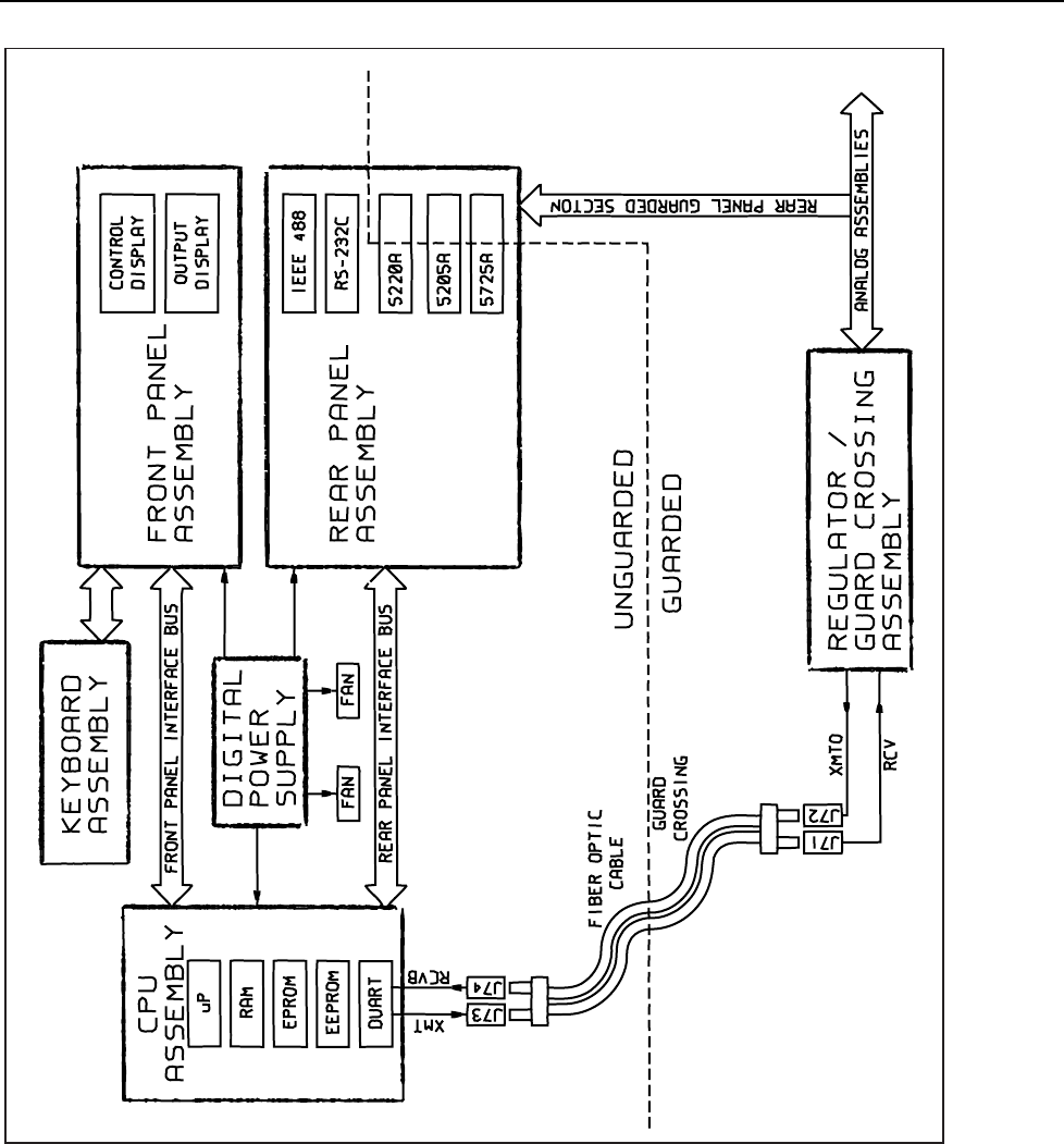
Theory of Operation
Analog Section Overview
2
2-7
ahp003f.eps
Figure 2-1. Digital Section Block Diagram

5700A/5720A Series II Calibrator
Service Manual
2-8
These analog assemblies are interfaced to the Analog Motherboard assembly (A3). The
guarded digital bus generated by the guard crossing portion of the Regulator/Guard
Crossing assembly controls all analog assemblies except the Filter/PA Supply. The
Guard Crossing interfaces with the unguarded CPU assembly via a fiber-optic link. The
Transformer assembly, along with the filter portion of the Filter/PA Supply assembly
and the regulator portion of the Regulator/Guard Crossing assembly, create the system
power supply for all the analog assemblies. The Power Amplifier Supply portion of the
Filter/PA Supply assembly provides the high voltage power supplies required by the
Power Amplifier assembly. The amplitudes of these high voltage supplies are controlled
by circuitry contained on the Power Amplifier assembly.
Figures 2-2 and 2-3 are block diagrams for the analog section of the Calibrator.
2-9. Functional Description Presented by Output Function
This part of the theory section presents Calibrator operation from the perspective of each
output function. It describes which assemblies come into play, and how they interact. It
does not provide a detailed circuit description. Refer to the individual assembly theories
further on in this section for detailed circuit descriptions.
2-10. DC Voltage Functional Description
The DAC assembly (A11) provides a stable dc voltage and is the basic building block of
the Calibrator. DC voltages are generated in six ranges:
• 220 mV
• 2.2V
• 11V
• 22V
• 220V
• 1100V
The 11V and 22V ranges are generated by the DAC assembly, with its output, DAC
OUT HI and DAC SENSE HI routed to the Switch Matrix assembly, where relays
connect it to INT OUT HI and INT SENSE HI. Lines INT OUT HI and INT SENSE HI
connect to the Calibrator binding posts by relays on the Analog Motherboard assembly
(A3).
The 2.2V range is created on the Switch Matrix assembly by resistively dividing by five
the 11V range from the DAC assembly. Relays on the Switch Matrix and Analog
Motherboard route the 2.2V range output to the Calibrator binding posts.
The 220 mV range is an extension of the 2.2V range. The Switch Matrix assembly
resistively divides by ten the 2.2V range to create the 220 mV range. Relays on the
Switch Matrix and Analog Motherboard route the 220 mV range output to the front
panel binding posts.
The 220V range is generated by the DAC and Power Amplifier assemblies. The Power
Amplifier amplifies the 11V range of the DAC assembly by a gain of -20 to create the
220V range. The output of the Power Amplifier is routed to the High Voltage Control
assembly (A14), where a relay connects it to PA OUT DC. Line PA OUT DC is routed
to the binding posts via relays on the Switch Matrix and Analog Motherboard.
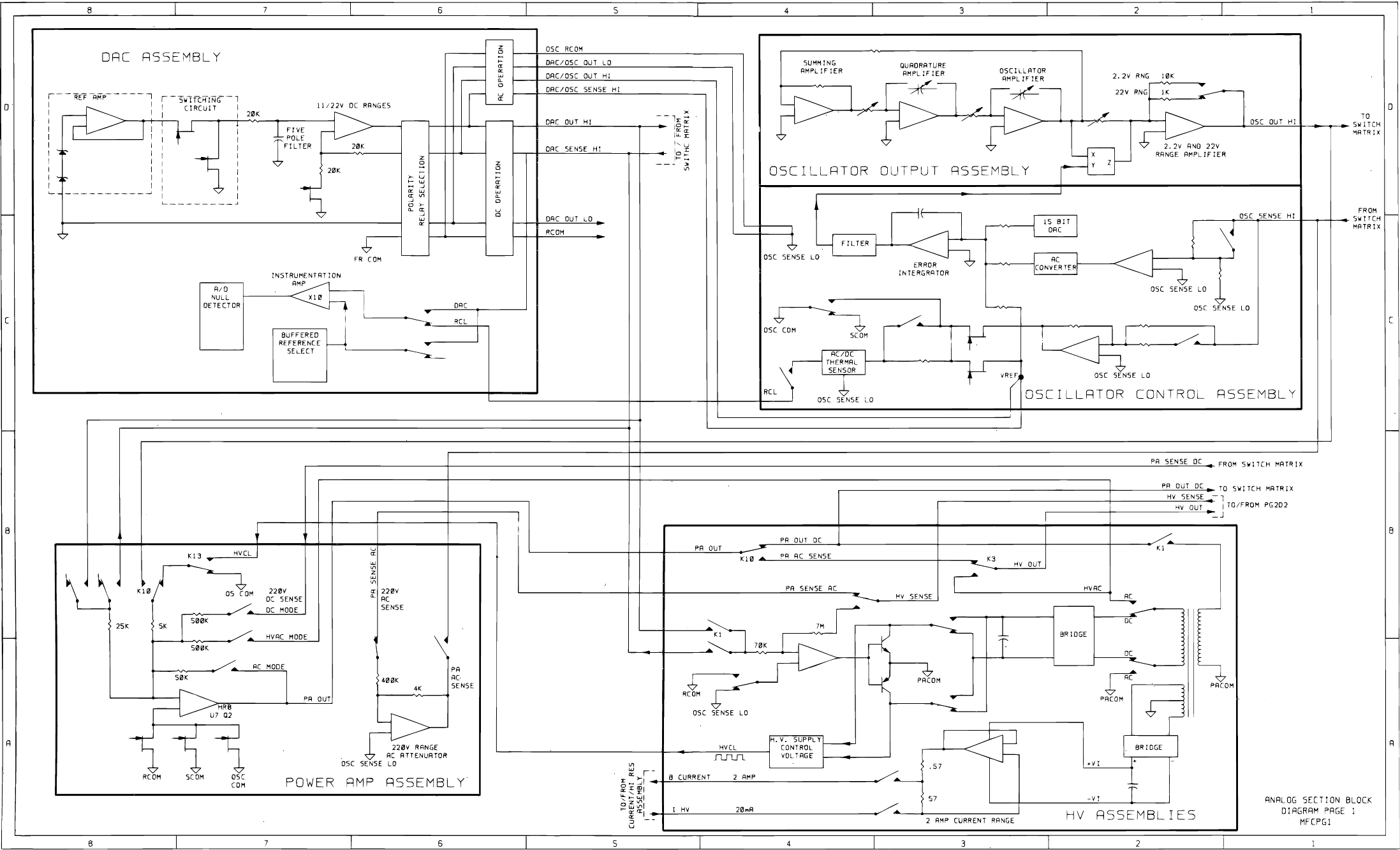
2
Theory of Operation
2-9
Theory of Operation
Figure 2-2. Analog Section Block Diagram, Part 1
ahp33f.eps
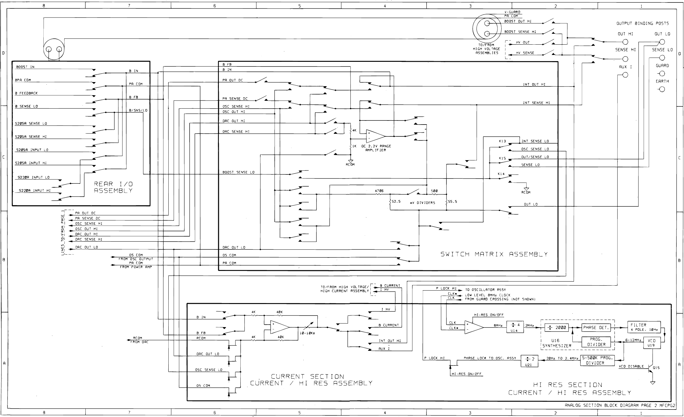
5700/5720A Series II Calibrator
Service Manual
ahp34f.eps
Figure 2-3. Analog Section Block Diagram, Part 2
2-10

Theory of Operation
Functional Description Presented by Output Function
2
2-11
The 1100V range is generated by the High Voltage/High Current assembly (A15)
operating in conjunction with the Power Amplifier assembly and the High Voltage
Control assembly. The 11V range of the DAC assembly is routed to the High
Voltage/High Current assembly which amplifies by a gain of -100 to create the 1100V
range. Basically the high voltage output is obtained by rectifying and filtering a high
voltage ac signal generated by the High Voltage Control assembly operating in
conjunction with the Power Amplifier assembly.
2-11. AC Voltage Functional Description
The Oscillator Output assembly (A13) is the ac signal source for the Calibrator. The
Oscillator Control assembly (A12), controls the amplitude of this ac signal by comparing
it with the accurate dc voltage from the DAC assembly and making amplitude
corrections via the OSC CONT line. The frequency of oscillation is phase locked to
either the high resolution oscillator on the Current/Hi-Res (A7) assembly or an external
signal connected to the PHASE LOCK IN connector on the rear panel. AC voltages are
generated in the following ranges:
• 2.2 mV
• 22 mV
• 220 mV
• 2.2V
• 11V
• 22V
• 220V
• 1100V
The 2.2V and 22V ranges are generated by the Oscillator Output assembly and routed to
the Calibrator binding posts via relays on the Switch Matrix (A8) and Analog
Motherboard assemblies.
The 220 mV range is generated on the Switch Matrix assembly, which resistively divides
by ten the 2.2V range of the Oscillator Output assembly. Relays on the Switch Matrix
and Analog Motherboard route the 220 mV range to the Calibrator binding posts.
The 2.2 mV and 22 mV ranges are generated on the Switch Matrix assembly. In this
mode, the Switch Matrix resistively divides the 2.2V range or the 22V range by 1000 to
create the 2.2 mV and 22 mV ranges respectively. Relays on the Switch Matrix and
Analog Motherboard route these ranges to the Calibrator binding posts.
The 220V range is generated on the Power Amplifier assembly. In this mode, the Power
Amplifier is set for a nominal gain of -10 to amplify the 22V range from the Oscillator
Output to the 220V range. The 220V ac range from the Power Amplifier is routed to the
Calibrator binding posts by relays on the High Voltage Control assembly and the Analog
Motherboard.
The 1100V range is generated by the High Voltage Control assembly operating in
conjunction with the Power Amplifier assembly. In this mode, the 22V range from the
Oscillator Output is amplified by the Power Amplifier and High Voltage Control
assemblies, which create an amplifier with a nominal gain of -100. Relays on the High
Voltage Control and Analog Motherboard assemblies route the 1100V ac range to the
Calibrator binding posts.

5700A/5720A Series II Calibrator
Service Manual
2-12
2-12. Wideband AC V Functional Description (Option -03)
The Wideband AC Voltage module (Option -03) consists of the Wideband Oscillator
assembly (A6) and the Wideband Output assembly (A5). There are two wideband
frequency ranges:
• 10 Hz to 1.1 MHz
• 1.2 MHz to 30 MHz
During operation between 10 Hz and 1.1 MHz, output from the Oscillator Output
assembly is routed to the Wideband Output assembly where it is amplified and
attenuated to achieve the specified amplitude range. The output is connected to the
Calibrator front panel WIDEBAND connector. Operation between 1.2 MHz and 30 MHz
works the same way, except the input to the Wideband Output assembly is the ac signal
from the Wideband Oscillator assembly.
2-13. DC Current Functional Description
DC current is generated in five ranges:
• 20 µA - 220 µA
• 220 µA - 2.2 mA
• 2.2 mA - 22 mA
• 22 mA - 220 mA
• 2.2A
All current ranges except 2.2A are generated by the current portion of the Current/Hi-
Res assembly. These currents are created by connecting the output of the DAC assembly,
set to the 22V range, to the input of the Current assembly. The Current assembly uses
this dc voltage to create the output current. The current output can be connected to the
AUX CURRENT OUTPUT binding post by relays on the Current assembly, to the
OUTPUT HI binding post by relays on the Current, Switch Matrix, and Analog
Motherboard assemblies, or to the 5725A via the B-CUR line by relays on the Analog
Motherboard assembly and Rear Panel assembly.
The 2.2A range is an extension of the 22 mA range. The 22 mA range output from the
Current assembly is amplified by a gain of 100 by the High Voltage/High Current
assembly operating in conjunction with the Power Amp assembly and the High Voltage
Control assembly. The 2.2A current range is routed back to the Current assembly where
it is connected to either the AUX CURRENT OUTPUT binding post, the OUTPUT HI
binding post, or the 5725A in the same manner as the lower current ranges.
2-14. AC Current Functional Description
AC current is created in the same manner as dc current, except the input to the Current
assembly is the ac voltage from the Oscillator Output assembly set to the 22V range. The
switching between ac and dc is carried out on the Switch Matrix, Oscillator Control,
Oscillator Output, and DAC assemblies.

Theory of Operation
System Interconnect Detailed Circuit Description
2
2-13
2-15. Ohms Functional Description
Two assemblies function as one to supply the fixed values of resistance:
• Ohms Main assembly (A10)
• Ohms Cal assembly (A9)
All of the resistance values except the 1Ω, 1.9Ω, and short are physically located on the
Ohms Main assembly. The 1Ω, 1.9Ω, and short are physically located on the Ohms Cal
assembly. The desired resistance is selected by relays on these Ohms assemblies and is
connected to the Calibrator binding posts by relays on the Analog Motherboard. The
Ohms Cal assembly also contains the appropriate circuitry to enable the Calibrator to
perform resistance calibration. Once calibrated, the Calibrator output display shows the
true value of the resistance selected, not the nominal (e.g., 10.00031 kΩ, not 10 kΩ).
Four ohms measurement modes are available. For the two-wire configuration,
measurement with or without lead-drop compensation sensed at the binding posts of the
UUT (using the SENSE binding posts and another set of leads), or at the ends of its test
leads is available for 19 kΩ and below. Four-wire configuration is available for all but
the 100 MΩ value.
2-16. System Interconnect Detailed Circuit Description
The motherboard assembly contains the Digital Motherboard assembly (A4), and the
Analog Motherboard assembly (A3). These two Motherboards are mechanically fastened
together with screws. They are electrically connected by connectors P81 and P82 on the
Digital Motherboard and connectors J81 and J82 on the Analog Motherboard. AC
voltage taps from the Transformer assembly (A22) are connected to the Analog
Motherboard through these connectors. Refer to Figure 2-4 for an overview of system
interconnections. Figure 2-4 continues on the reverse side, showing system grounds.
2-17. Digital Motherboard Assembly (A4)
The Digital Motherboard contains the line-select switches, line fuse, power switch, a
fiber-optic transmitter (J73), and a fiber-optic receiver (J74). It also contains connectors
for the Transformer assembly (A22), Digital Power Supply assembly (A19), CPU
assembly (A20), Front Panel assembly (A2), Rear Panel assembly (A21), and the two
24V dc fans mounted in the chassis.
The fiber-optic receiver and transmitter provide the serial communication link between
the CPU on the unguarded Digital Motherboard and the Regulator/Guard Crossing on the
guarded Analog Motherboard.

5700A/5720A Series II Calibrator
Service Manual
2-14
2-18. Transformer Assembly (A22)
The Transformer assembly receives ac line inputs routed through the A4 Digital
Motherboard. This assembly supplies outputs throughout the Calibrator, all of which are
routed through the A4 Digital Motherboard.
The Transformer assembly, the filter portion of the Filter/PA Supply assembly (A18),
and the regulator portion of the Regulator/Guard Crossing assembly (A17) create the
system power supply for all analog assemblies. The Transformer assembly also supplies
ac voltages to the Digital Power Supply assembly which generates five regulated dc
voltages for use by the CPU, Front Panel assembly, Rear Panel assembly, and the
cooling fans.
2-19. Analog Motherboard Assembly (A3)
The Analog Motherboard contains the connectors for all assemblies in the guarded
section of the calibrator. The Analog Motherboard also contains 13 relays, a fiber-optic
transmitter, a fiber-optic receiver, a cable for binding post connections, and two cables
for the interface to the Rear Panel assembly. Table 2-1 lists Analog Motherboard
The fiber-optic transmitter (J72) and the fiber-optic receiver (J71) provide the serial
communication link between the Regulator/Guard Crossing assembly and the CPU
assembly on the unguarded Digital Motherboard.
Control lines for relays K1-K10 and K13 on the Analog Motherboard assembly are
generated on the Switch Matrix (A8) assembly. Control line RLY11*, which controls
relay K11, is generated on the Current/Hi-Res assembly (A7). Control line RLY12*,
which controls relay K12, is generated on the Rear Panel assembly (A21).
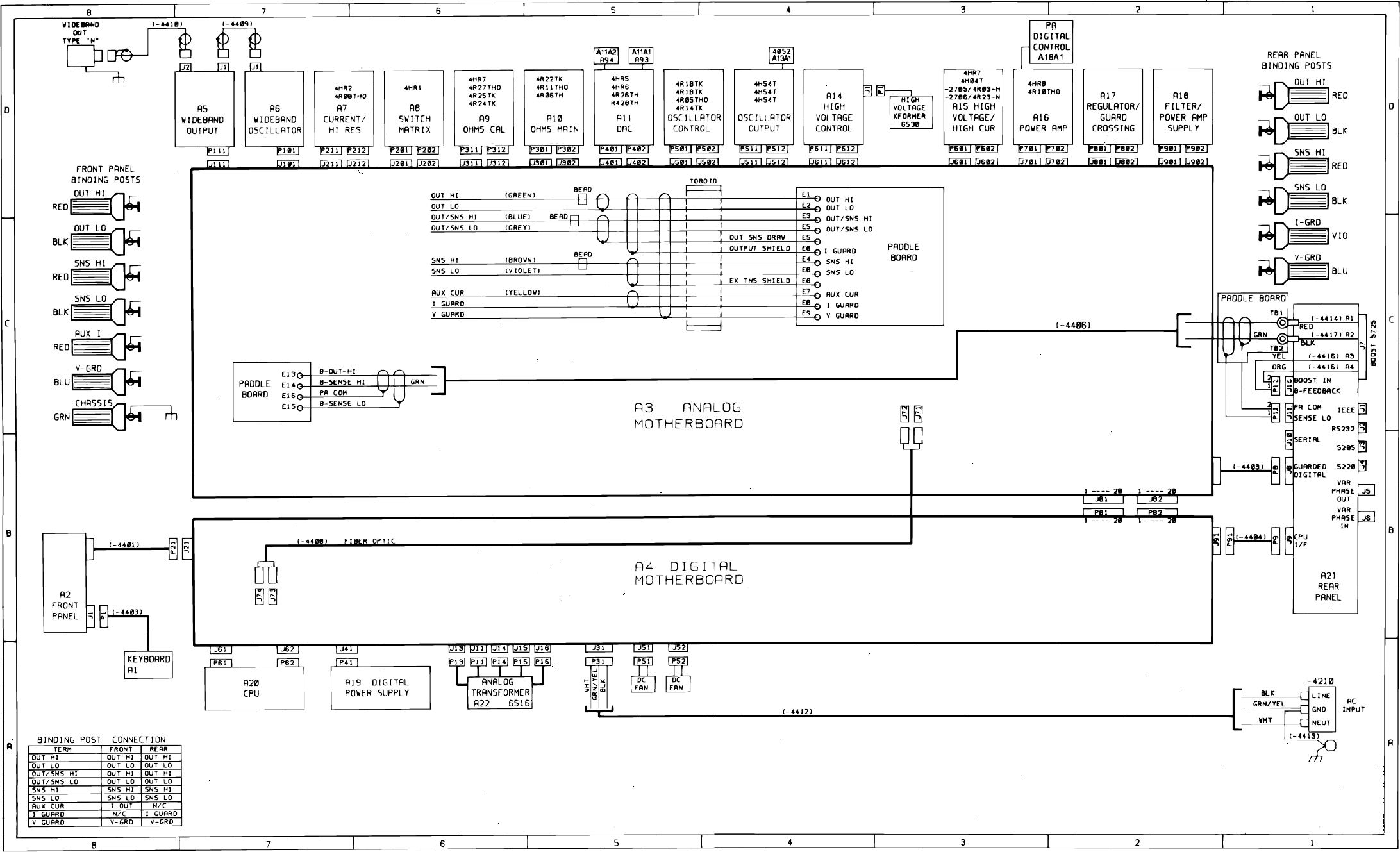
2
Theory of Operation
ahp35f.eps
2-15
Functional Description Presented by 0utput Function
Figure 2-4. System Interconnections
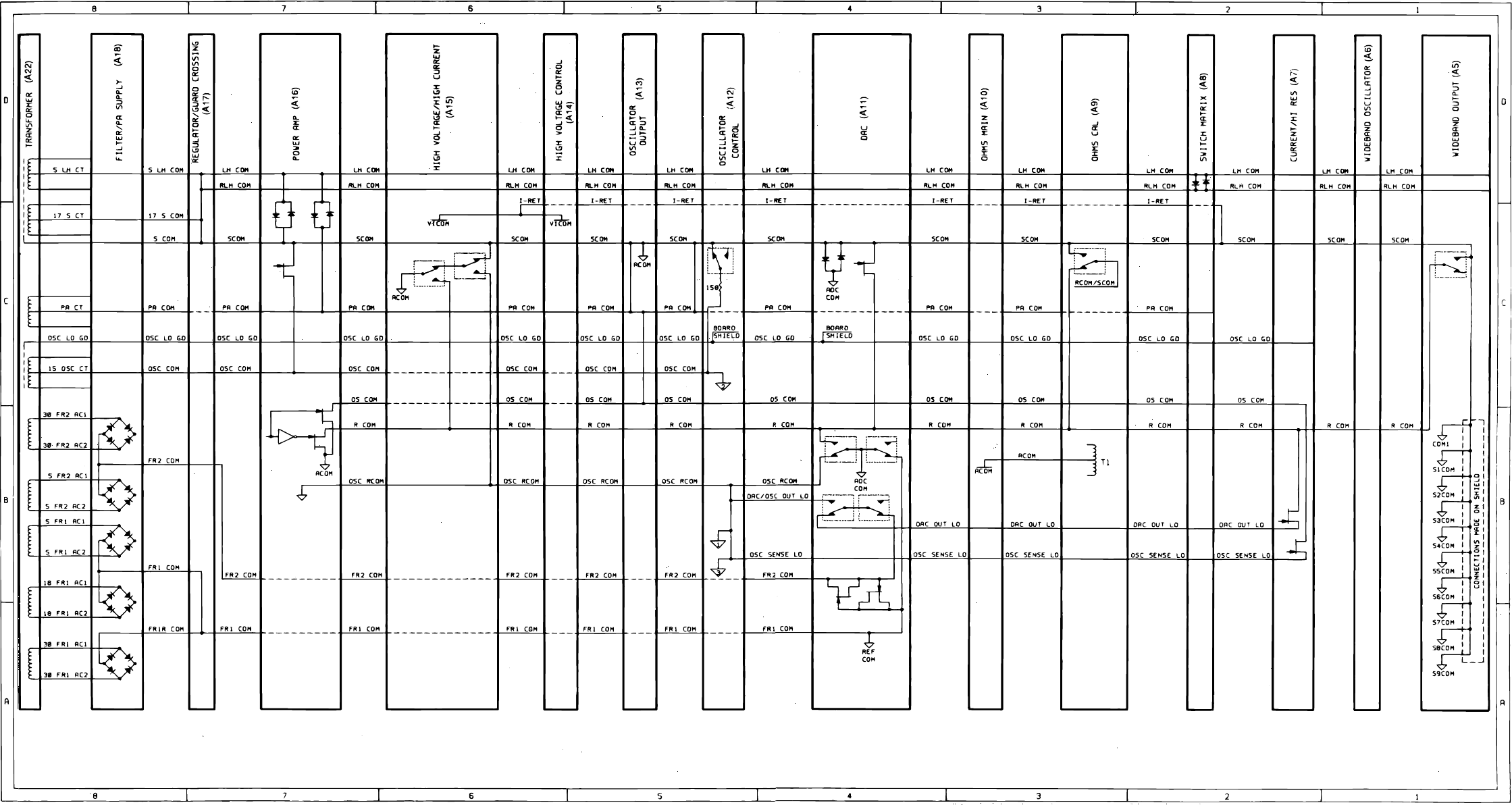
5700/5720A Series II Calibrator
Service Manual
2-16
Figure 2-4. System Interconnections (cont)
ahp35f.eps

Theory of Operation
System Interconnect Detailed Circuit Description
2
2-17
Table 2-1. Analog Motherboard Connectors
Motherboard Connector Connected to Assembly
J101 Wideband Oscillator Assembly (A6)
J111 Wideband Output Assembly (A5)
J201 and J202 Switch Matrix Assembly (A8)
J211 and J212 Current/Hi-Res Assembly (A7)
J301 and J302 Ohms Main Assembly (A10)
J311 and J312 Ohms Cal Assembly (A9)
J401 and J402 DAC Assembly (A11)
J501 and J502 Oscillator Control Assembly (A12)
J511 and J512 Oscillator Output Assembly (A13)
J601 and J602 High Voltage/High Current Assembly (A15)
J611 and J612 High Voltage Control Assembly (A14)
J701 and J702 Power Amplifier Assembly (A16)
J801 and J802 Regulator/Guard Crossing Assembly (A17)
J901 and J902 Filter/PA Supply Assembly (A18)
Line INT OUT HI is the calibrator output for ac voltage operation in the 22V range and
below, dc voltage operation in the 220V range and below, all resistance functions, and
all ac/dc current ranges. Relays on the Current assembly route the current output to the
AUX CURRENT OUTPUT binding post via the I OUT line if so selected by the
operator. INT SENSE HI is the sense high path during these modes of operation. INT
OUT HI is connected to the OUTPUT HI binding post through relay K1. INT SENSE HI
is connected to the SENSE HI or OUTPUT HI binding post through relays K2 and K3.
Line HV OUT is the calibrator output for dc voltage operation in the 1100V range, and
ac voltage operation in the 220V and 1100V ranges. Line HV SENSE is the sense high
path during these modes of operation. HV OUT is connected to the OUT HI binding post
through relays K9 and K1. HV SENSE is connected to the SENSE HI or OUTPUT HI
binding post through relays K10, K2, and K3.
The 5725A Amplifier output is B OUT HI and the sense high path is B SNS HI. When
the 5725A is active, B OUT HI is connected to the OUT HI binding post through relays
K4 and K1. When the 5725A Amplifier is inactive, B OUT HI is connected to GUARD
CHASSIS by relay K12. Line B SNS HI is tied to B OUT HI through diode clamps CR1
and CR2 and is connected to the SENSE HI or OUTPUT HI binding post through relays
K5, K2, and K3.
The cable from the motherboard to the binding posts consists of six insulated wires and
six shields, each with its own drain wire. The OUT HI line, SENSE HI line,
OUT/SENSE HI line and AUX CURRENT line each connect to an insulated wire and
each has a shield around the wire. These shields are connected to OUT LO, SENSE LO,
OUT/SENSE LO, and I/V GUARD, respectively. The I/V GUARD line is connected to I
GUARD during operation in the current mode or V GUARD during operation in the
voltage mode. This selection is done by relay K11.
When the Calibrator is in standby, all binding posts are open-circuited except the
GROUND binding post. In addition, GUARD CHASSIS is connected to S COM by K6.
When in the operate condition, this connection is broken (K6 energized) and GUARD
CHASSIS is connected to V GUARD via K7, which goes to the GUARD binding post,
and to OUT LO via K8. GUARD CHASSIS is also connected to OSC LO GD by K13
except during ac or dc millivolt operation, when instead OSC LO GD is connected to S
COM.

5700A/5720A Series II Calibrator
Service Manual
2-18
2-20. Front/Rear Binding Posts
An internal cable can be configured to enable either the front panel or panel binding
posts. When compared to front panel binding posts, the rear panel provides the same
OUTPUT HI, OUTPUT LO, SENSE HI, SENSE LO, AND V GUARD functions. Also,
the rear panel provides an I GUARD (current guard) connection for use when the
Calibrator is supplying low-level ac current through a long cable. Use of the I GUARD
connection removes errors introduced by leakage through such cables. The rear panel
binding posts do not provide an AUX CURRENT OUTPUT connection. The procedure
to disable the front panel binding posts and enable the rear panel binding posts is to be
done at Service Centers, although it is described in this manual in Section 4.
2-21. Rear Panel Assembly (A21)
The Rear Panel assembly provides physical and electrical connections for the auxiliary
amplifiers, along with RS-232-C and IEEE-488 interface connections. Relays on the
Rear Panel assembly are used as the interfaces for the 5725A amplifier, or for switching
the PHASE LOCK IN and VARIABLE PHASE OUT signals.
A 5725A auxiliary amplifier can be physically connected to the Rear Panel assembly of
the 5700A/5720A Series II at J7. Only one amplifier can be in use at one time.
• The Rear Panel assembly provides relay switching for 5725A signals. Voltage
outputs from the 5725A are routed to the binding posts on the Calibrator. Current
outputs are soured at the 5725A OUTPUT binding posts. An alternate configuration
is also available, allowing for routing of Calibrator current outputs to the 5725A
OUTPUT binding posts.
2-22. Filter PA Supply Assembly (A18)
The Filter/PA Supply assembly incorporates two sections. The first section contains
filters and regulators for some of the in-guard low-voltage supplies, and the second
contains the power supply for the Power Amplifier output. Theory for each section is
discussed separately.
2-23. Digital Section Detailed Circuit Description
Detailed descriptions of each assembly in the digital section are provided here.
Simplified schematics and block diagrams are provided to supplement the text.
2-24. Digital Power Supply Assembly (A19)
The Digital Power Supply assembly receives ac voltages from the transformer and
provides five regulated dc voltages for use by the CPU, Front Panel assembly, Rear
Panel assembly, and the cooling fans. All power supply voltages are referenced to
COMMON, which is the transformer center tap for the ±12V supplies. Test points at the
top of the assembly can be used to check unregulated input voltages, and regulated dc
output voltages. Table 2-2 lists the supplies generated by the Digital Power Supply.

Theory of Operation
Digital Section Detailed Circuit Description
2
2-19
Table 2-2. Supplies Generated by the Digital Power Supply
Signal Name Test Point Nominal
Output Tolerance Current
Limit Rated
Output
+75V OUT TP2 73V +/-8% 121 mA 100 mA
+35V OUT TP5 35V +/-7% 52 mA 40 mA
+12 VOLTS TP8 12V +/-5% 1.5A 700 mA
-12 VOLTS TP10 12V +/-5% 1.5A 450 mA
+5V TP12 5.2V +/-5% 2.4A 2.0A
COMMON TP13
2-25. +5V Power Supply
The unregulated +5V supply uses CR25-CR28 in a full-wave rectifier configuration with
filter capacitors C12, C13, and C14. Capacitors C20 and C21 filter out high-frequency
noise. Inductor L8 is a common-mode choke and C11 is a bypass capacitor. The
regulator is fused by 3.15A slow-blow fuse F5.
The regulated +5V is generated by three-terminal low-dropout +5V regulator U3 with
heat sink. The regulator’s output voltage is increased about 0.2V by CR35, a germanium
diode connected between the regulator’s ground pin and COMMON. Capacitor C14 is
for bypass. Capacitor C23 filters out high-frequency noise. Diode CR29 protects the
regulator against input shorts, and diode CR30 protects the regulator from reverse
voltage. Inductor L7 and C16 further filter the output to P41.
2-26. ±12V Power Supplies
A full-wave rectifier made of diodes CR17-CR20 and filter capacitors C6 and C7
generate the unregulated +12V and -12V supplies. AC inputs are fused by F3 and F4,
both 2A slow blow.
The regulated +12V supply is generated by a three-terminal +12V regulator U1 with heat
sink. Capacitors C5 and C9 are for bypass. Diode CR21 protects the regulator from input
shorts, and diode CR23 protects the regulator from reverse voltage. Capacitor C22 filters
out high frequency noise.
Three-terminal -12V regulator U2 with heat sink generates the regulated -12V supply.
Capacitors C8, C10, and C19 are for bypass. Diode CR22 protects the regulator from
input shorts, and diode CR24 protects the regulator from reverse voltage.
Inductors L3-L6 filter the regulated outputs. R7 further isolates the ±12V FAN lines
from the ±12V power lines. The +12V FAN and -12V FAN lines power the two 24V dc
fans inside the calibrator.
2-27. +35V Power Supply
The +35V power supply powers the grid drivers and anode drivers on the front panel
output display circuitry.
A full-wave rectifier made of diodes CR9-CR12 and filter capacitor C3 generate the
unregulated +35V supply. Its input is fused by F2, a 0.125A slow-blow. Capacitor C18 is
for bypass. Capacitor C25 filters out high frequency noise.
Zener diodes VR14, VR15 and transistor Q5 generate the +35V regulated output. Zener
diodes VR14 and VR15 (both 18V) make up the control element which sets the output
voltage. Transistor Q5 is used as an emitter follower. CR13 is the constant current source
supplying current to the zener diodes and the base of Q5. Components R5 and Q6 make
up the current-limiting circuit. During an over-current condition, the voltage drop across
R5 turns Q6 on, thus drawing current away from the base of Q5 and limiting current

5700A/5720A Series II Calibrator
Service Manual
2-20
flow to the output. Diode CR16 protects this circuit from reverse voltage and C4 is a
bypass capacitor. Inductor L2 filters the regulated output. Resistor R13 is a bleed-off
resistor for C3.
2-28. +75V Power Supply
The +75V power supply powers the grid drivers and anode drivers on the front panel
control display circuitry.
A full-wave rectifier made of diodes CR1-CR4 and filter capacitor C1 generate the
unregulated +75V supply. Its input is fused by F1, a 0.315A slow-blow. Capacitor C17 is
for bypass. Capacitor C24 filters out high frequency noise.
The +75V regulated output is generated by 36V zener diode VR6, 39V zener diode VR7,
and transistors Q1 and Q3. Zener diodes VR6 and VR7 set the output voltage.
Transistors Q1 and Q3, in a Darlington configuration for current gain, are used as an
emitter follower. Transistor Q4, zener diode VR5, and resistors R2 and R3 make up the
constant current source supplying current to the zener diodes and the base of Q3. Current
limiting is performed by R1 and Q2 in the same manner as in the +35V supply. Diode
CR8 protects the circuit from reverse voltage and C2 is a bypass capacitor. Inductor L1
filters the regulated output. Resistor R6 is a bleed-off resistor for C1.
2-29. +35V and +75V Shut-Down Circuit
The +35V and +75V high voltage supplies are shut down when a fault occurs in the
control display refresh circuitry. This shut-down circuit prevents the Control Display and
Output Display from burning out, and also verifies that the master clock is generating
control signals for both displays.
During normal operation, 75VSD is low, turning Q10 off. Line RESETL pulls the base
of Q9 high through R9, turning Q9 on. This action in turn pulls the junctions of CR31-
CR32 and CR33-CR34 low, turning Q7 and Q8 off. The +75V and +35V constant-
current sources can then supply the appropriate zener diodes and drive the bases of the
respective emitter followers.
When a display refresh fault occurs, the 75VSD line on P41 pin 5C, coming from the
Front Panel assembly, goes high. this signal, pulled up by R4, drives the base of Q10
through base resistor R11. Transistor Q10 then saturates, pulling the base of Q9 near
ground, turning Q9 off. On power-up or during a CPU reset, the RESETL signal is low,
pulling the base of Q9 near ground through R9, also turning Q9 off. Resistor R12 is a
turn-off resistor for Q9. Diodes CR31 and CR33 are in a wired-OR configuration. When
Q9 is saturated (on), CR31 and CR33 pull their respective junctions to CR32 and CR34
near ground, turning Q7 and Q8 off. When Q9 is off, the junctions are pulled high
through R8 and R10, saturating Q7 and Q8 (on). When on, Q7 removes the base drive
from Q3, shutting down the +75V supply. Similarly, Q8 removes the base drive from
Q5, shutting down the +35V supply.
Diodes CR32 and CR34 simply ensure that Q7 and Q8 are off when Q9 is on. Resistor
R8 guarantees that Q7 will hold the +75V supply off until it drops below 15.6V, and R10
holds the +35V supply off to 7.8V.

Theory of Operation
Digital Section Detailed Circuit Description
2
2-21
2-30. CPU (Central Processing Unit) Assembly (A20)
The CPU (Central Processing Unit) for the Calibrator is a single-board computer based
on a 68HC000 microprocessor. The CPU assembly communicates with the Guarded
Digital section, the Front Panel assembly, and the Rear Panel assembly. The board can
be divided into three primary areas:
• The microprocessor and its support circuitry
• Memory
• Peripheral chips and I/O interfaces
Microprocessor support circuitry consists of a power-up and reset circuit, clock
generation, a watchdog timer, address decoders and DTACK (data acknowledge)
generator, bus error timeout, and interrupt controller.
Figure 2-5 is a block diagram of the CPU assembly. Table 2-3 is a glossary of the
acronyms used in the text and schematic for the CPU assembly.
2-31. Power-Up and Reset Circuit
The power-up and reset circuitry consists of line monitor chip U1, C5, C6, CR1, R3, Z3,
switch SW1, and inverters on U2. This circuit provides a 195 ms reset pulse at power-up
or upon pressing and releasing SW1, placing the CPU assembly in a known safe
condition. If the power supply glitches or falls below 4.55V ±0.05V, U1 resets the
Calibrator. The reset pulse duration is determined by C5. Note that SW1 performs a
different function than the front panel RESET button. SW1 is a hardware reset that is
hard-wired to and directly read by the microprocessor. The front panel RESET button is
a software reset; it tells the system software to restore the Calibrator configuration to a
default condition.
The heart of this circuit is the line monitor chip U1. On power-up or when SW1 is
pushed, U1 forces an active-low reset pulse on RESETL and an active-high pulse on
RESET. RESETL helps to prevent accidental writes to EEPROM and drives an inverter
in U2 to turn off LED CR1. CR1 indicates that the +5V supply is on and that the CPU is
operating, i.e. not reset. RESETL also resets the rear panel assembly. The other output,
RESET, drives two inverters in U2. One of these inverters provides HALT*. The other
generates IORESET*, which drives the processor's RESET, and provides a reset for the
front panel interface and DUARTs (dual universal asynchronous receiver/transmitter)
circuitry.
2-32. Clock Generation
The clock generation circuit uses components Y1, Y2, U3, U4, R4, R5, C8, C9, and E5.
The crystal Y1, along with the resistors, capacitors, and an inverter in U3 generates the
7.3728 MHz primary system clock CLK. This system clock is used by the processor and
is divided down by a binary counter (U4) for clocks of 3.6864 MHz, 28.8 kHz, and 450
Hz. The 450 Hz clock is used by the watchdog timer, the 28.8 kHz is used by U6 in the
decoding circuit, and the 3.6864 MHz is used by the DUARTs, and the clock filter
circuit. Jumper E5 allows for selection of the alternate oscillator (Y2) as the system
clock.

5700A/5720A Series II Calibrator
Service Manual
2-22
ahp004f.eps
Figure 2-5. CPU Assembly Block Diagram

Theory of Operation
Digital Section Detailed Circuit Description
2
2-23
Table 2-3. CPU Acronym Glossary
Signal Name Function
A01-A23 Address lines
ADCLKCS* Clock/calendar (U33) chip select
AS* Address strobe
BERR* Bus error
BGACK* Bus grant acknowledge
BR* Bus request
BRPDRTINT* Rear panel DUART interrupt
BRPDTK* Rear panel data transfer acknowledge
BRPIEEEINT* Rear panel IEEE-488 interrupt
CLKCALINT* Clock/calendar interrupt
D00-D15 Data lines
DOGCLR Dog clear (clears watchdog timer)
DOGINTH Dog interrupt (interrupt from watchdog timer)
DRTDTK* DUART data transfer acknowledge
DTACK* Data transfer acknowledge
E Enable for 6800 family devices (737.28 kHz clock)
EXDUARTINT* External DUART Interru
FAN1 Signal monitoring fan 1
FAN2 Signal monitoring fan 2
FANINT* Fan monitor interrupt
FC0 Function code output 0
FC1 Function code output 1
FC2 Function code output 2
FPDTK* Front panel data transfer acknowledge
FRNTPNLCS* Front panel chip select
FRNTPNLEN* Front panel enable
GCDRTCS* Guard crossing DUART chip select
GCDUARTINT* Guard crossing DUART interrupt
INTRCNTL1 Interrupt control 1
INTRCNTL2 Interrupt control 2
IPL0* Interrupt priority level 0
IPL1* Interrupt priority level 1
IPL2* Interrupt priority level 2
KEYBRDINT* Keyboard interrupt
LDS* Lower data strobe
MISCCS* Miscellaneous chip select enable (upper address bits decoder)
NVMCS* Nonvolatile memory chip select
NVMOE* Nonvolatile memory output enable
PROM0CS* PROM 0 chip select (U15 and U16)
PROM1CS* PROM 1 chip select (U17 and U18)
PROM2CS* PROM 2 chip select (U23 and U24)
PSFAILINT* Power supply fail interrupt
RAM0CS* RAM chip select (U19 and U20)
RAM1CS* RAM chip select (U21 and U22)
RAM2CS* RAM chip select (U40 and U41)
R/WR* Read/write
RDINT* Read interrupt
RDL* Read data lower
RDU* Read data upper
RDY/BSYL Ready/busy
RPSEL* Rear panel chip select
RRPNLEN* Rear panel enable
RXDA Receive Data Port A
RCVB Receive Data Port B
SCLK Serial clock
TXDA Transmit Data Port A
TXDB Transmit Data Port B
UDS* Upper data strobe
WRL* Write lower
WRU* Write upper
XDUARTCS* External DUART chip select

5700A/5720A Series II Calibrator
Service Manual
2-24
2-33. Watchdog Timer
The watchdog timer circuitry uses a 74HC4020 binary counter (U11) to divide the 450
Hz from the clock generation circuit to produce interrupt DOGINTH, signifying that the
system may be locked up. This interrupt is generated 1.14 seconds after the last
DOGCLR2 signal from interrupt controller U10. Therefore, DOGCLR2 must occur more
often then every 1.14 seconds to clear U11 and prevent the watchdog interrupt.
Generation of DOGCLR2 is under software control. The watchdog timer can be disabled
by cutting jumper E1.
2-34. Address Decoding and DTACK (Data Acknowledge)
Two Programmable Logic Devices (PLDs) accomplish address decoding and DTACK
(data acknowledge) generation. ICs U5 and U6 provide chip selects and generate
acknowledgment signals for those devices without DTACK lines. IC U5 receives
DTACK signals from the asynchronous devices and ORs these signals together to form
DTACK*. Table 2-4 is the memory map for the system. It shows the chip select, address
range, and notes whether AS* (address strobe) or LDS* (lower data strobe) is required.
Table 2-4. CPU Memory Map
Chip Select Read/Write Address Range AS* or LDS* Required?
PROM0CS* R 0 to 3FFFF no
PROM1CS* R 40000 to 7FFFF no
PROM2CS* R 80000 to BFFFF no
RAM0CS* 600000 to 60FFFF no
RAM1CS* 610000 to 61FFFF no
RAM2CS* 620000 to 623FFF no
NVMCS* R/W C00000 to CFFFFF no
MISCCS* R/W D00000 to DFFFFF no
RPSEL* R/W D00000 to D01FFF LDS*
RPDUARTCS* R/W D00000 to D0001F LDS*
RPIEEECS* R/W D00020 to D0002F LDS*
Y52XXRD* R D00030 to D00031 LDS*
Y5205WR* W D00032 to D00033 LDS*
Y5220WR* W D00034 to D00035 LDS*
FRNTPNLCS* R/W D02000 to D03FFF AS*
OTDCS* R/W D02000 to D027FF AS*
DMDCS* R/W D02800 to D02FFF AS*
ENCODERCSR R D03000 to D033FF AS*
ENCODERRESETW W D03000 to D033FF AS*
LED_OUTPUT_ R R D03400 to D037FF AS
LED_LATCH_EN R/W D03400 to D037FF AS*
KEYBOARDCS R/W D03800 to D038FF AS*
GCDRTCS* D04000 to D05FFF LDS*
XDUARTCS* R/W D06000 to D07FFF LDS*
RDINT* W D08000 to D09FFF AS*
DOGCLR D08000 to D09FFF even only, AS*
ADCLKCS* E00000 to EFFFFF AS*

Theory of Operation
Digital Section Detailed Circuit Description
2
2-25
2-35. Interrupt Controller
PLD U10 is the priority interrupt controller. The interrupt controller reads incoming
interrupts and interrupt control lines, then encodes the highest priority interrupt into the
interrupt level for the 68HC000. When the 68HC000 responds to an interrupt request, it
asks the interrupt controller for an 8-bit vector that corresponds to the pending interrupt
of highest priority. The interrupt controller responds with the 4 LSB’s of the vector
according to how it is programmed. The 4 MSB’s are pulled up on resistor network Z1.
Table 2-5 shows the interrupts, their priority levels, and vectors.
Table 2-5. CPU Interrupts, Priorities, and Vectors
Interrupt Priority Level Vector (Hex)
NMI 7 - (not used)
DOGINTH 6 F4
BRPDRTINT* 5 F6
GCDUARTINT* 5 F7
EXDUARTINT* 5 F8
CLKCALINT* 4 F5
BRPIEEEINT* 4 F9
KEYBRDINT* 3 FA
BPSFAILINT* 2 FB
FANINT* 0 FF (not used)
RDY/BSYL 0 FF (not used)
No interrupt 0 FF
2-36. Glue Logic
ICs U2, U3, and U9 form the glue logic circuit, which keeps various CPU functions
running properly. The four OR gates in U9 and an inverter in U3 use control signals
UDS*, LDS*, and R/WR* from the microprocessor to generate control signals WRU*,
WRL*, RDL*, and RDU*.
2-37. RAM (Random-Access Memory)
Random-access memory is contained in three pairs of sockets, U19 and U20, U21 and
U22, and U40 and U41. These sockets accommodate either 32K x 8 or 128K x 8 static
CMOS RAM modules (32KB or 128 KB each). The Calibrator is shipped with U19-U22
installed, using 32K x 8 parts and providing 128 KB of static RAM.
2-38. ROM (Read-Only Memory)
Read-only memory is contained in three pairs of sockets, U15-U16, U17-U18, and U23-
U24. These sockets accommodate 27010 EPROMS, 128K x 8 devices (128 KB each).
Jumpers allow 256 KB devices to be used in their place. The Calibrator is shipped with
U15-U18 installed, providing 512 KB of EPROM.

5700A/5720A Series II Calibrator
Service Manual
2-26
2-39. Electrically-Erasable Programmable Read-Only Memory (EEPROM)
IC U13 is an EEPROM. The socket accommodates a 32K x 8 device (32 KB of storage.)
A jumper is provided to allow an 8K x 8 (8 KB) device to be used in place of the 32 KB
device. The Calibrator is shipped with a 32KB EEPROM installed.
The EEPROM requires protection against inadvertent writes during power-up and
power-down sequences, which could corrupt calibration constants stored there by the
68HC000. The 32 KB EEPROM provides for software-controlled protection against
accidental writes.
Hardware is also used to further ensure data integrity. The EEPROMs are designed so
that writes to the device are prevented by holding the output enable line (NVMOE*) low.
Diodes CR5, CR6 and CR8, together with resistor R6, perform a wired-OR function for
three signals that control NVMOE*. Components R6, CR6 and C17 hold NVMOE* to a
valid logic low for typically 37.3 ms during power-up; 26.8 ms minimum, 49.6 ms
maximum. Diode CR7 provides a discharge path for C17 on power-down, allowing the
operator to quickly turn the Calibrator off then on again, without interfering with the
power-up charge time of the capacitor. Diode CR8 allows the normal microprocessor
read of the device to take place. And diode CR5 allows power monitoring IC U1 to hold
NVMOE* low when the +5V power supply drops below 4.5V on power-down or during
power glitches.
2-40. DUART (Dual Universal Asynchronous Receiver/transmitter) Circuit
The 68C681 DUART (U31) has several functions. Its primary function is to provide the
asynchronous serial lines that communicate with the Guarded Digital Controller over the
fiber-optic path off the Digital Motherboard. A 75451 driver chip (U32) drives the fiber-
optic transmitter on the digital Motherboard.
The DUART has 8 output lines that perform various functions. INTRCNTL1 and
INTRCNTL2 go to the interrupt controller and are fed back to the DUART inputs. These
are used by the interrupt controller to enable certain interrupts. Line SCLK is a test
output of the channel A serial clock.
The DUART monitors the EEPROM ready signal and the FANINT* signal. It also has a
spare serial channel that goes to connector J5. Components U44 and U43 convert the
TTL-level signals at the DUART to RS-232-C-level signals at J5.
The DUART generates its own DTACK signal, DRTDTK*, which is used by U5 to
generate system DTACK, DTACK*. A second DUART, U42, with associated RS-232-C
drivers and receivers is used only for test purposes. It generates its own DTACK, wire-
ORed to DRTDTK*.
2-41. Clock/Calendar Circuit.
Time and date information is stored in a battery-backed clock/calendar circuit consisting
of 32.768 kHz crystal Y3, 3V lithium battery BT1, clock/calendar IC U33, and
capacitors C10 and C11. The clock/calendar IC has the necessary circuitry internally to
switch operation from the power supply to battery BT1. Pull-up resistors in Z5 off U33
are to ensure low power operation when the +5V supply is off. U33 generates
CLKCALINT* under software control.

Theory of Operation
Digital Section Detailed Circuit Description
2
2-27
2-42. Clock Filter Circuit
The clock filter circuit generates a 3.6864 MHz 200 mV sine wave for the Rear Panel
and Front Panel assemblies. This circuit buffers the 3.6864 MHz Clock with an inverter
in U3. The circuit contains dc-blocking capacitor C80, two stages of a low pass LC filter
(L80 and C81, L81 and C82), transformer T51, and termination resistor R82.
2-43. CPU to Rear Panel Interface
Components U25, U26, U27, and connector P62 interface the CPU to the rear panel. Bi-
directional bus transceiver U26 buffers the data lines. Signal R/WR* controls the
transmission direction of the data lines, and RRPNLEN* is the chip enable. IC U25
buffers control lines BRPDRTINT*, BRPIEEEINT*, and BRPDTK*. U27, enabled by
RRPNLEN*, buffers address line A01-A05 and control lines WRL* and R/WR*.
Control lines RESETL, RPSEL*, TXDB, RCVB, and XMT go directly to connector P62.
2-44. CPU to Front Panel Interface
Components U25, U28, U29, U30 and connector P61 interface the front panel to the
CPU. Bi-directional bus transceiver U30 buffers the data lines. Control signal R/WR*
controls the transmission direction of the data lines, and FRNTPNLEN* is the chip
enable. IC U28, enabled by FRNTPNLEN*, buffers address lines A05-A12. IC U29, also
enabled by FRNTPNLEN*, buffers address lines A01-A04 and control line R/WR*. Two
sections of U25 in parallel buffer IORESET*, providing twice the drive current of a
single section, generating BRESET*. Three other sections of U25 buffer FPINT*,
FPDTK*, and PSFAILINT*. Control line FRNTPNLCS* goes directly to connector P61.
2-45. Fan Monitor
The fan monitor circuit detects whether one of the two fans is fully or partially shorted,
open-circuited, or drawing excessive current. Current-sense resistors on the Digital
Motherboard send analog signals FAN1 and FAN2 to the CPU through P61. FAN1 is
subtracted from FAN2 in U52D, and the difference is amplified before being sent to a
window comparator made up of U52B and U52C (plus associated resistors). Capacitors
C12 and C13 act as low-pass filters for the two signals, preventing spurious noise from
interfering with detection circuitry.
When the output of U52D is greater than +5V, the output of U52B goes low (to about -
11V); otherwise the output is high (about +11V). U52A takes the +5V and generates a -
5V reference for comparator U52C. When the output of U52D is more negative than -
5V, the output of U52C goes low (to about -11V); otherwise the output is high (about
+11V). The outputs of U52B and U52C are wire-ORed through CR2 and CR3, using
R52 and R53 to limit current sunk by the comparators when their respective outputs are
low. Schottky barrier diode CR4 converts the -11V outputs of the comparators, when
either is low, to a TTL-level logic low, which is the active (true) level of FANINT*.
When both fans are functioning properly, diodes CR2 and CR3 are reverse-biased,
effectively taking the comparators out of the circuit. At this point, R51 pulls FANINT*
to a valid TTL-level logic high, the inactive state of FANINT*. R51 and CR4 level-shift
the ±11V signal to valid TTL levels.
Signal FANINT* goes to DUART U31 and to the interrupt controller U10 for further
processing. System software monitors FANINT* through U31, and can program the
DUART to generate a GCDUARTINT* interrupt signal on FANINT* going low.

5700A/5720A Series II Calibrator
Service Manual
2-28
2-46. Front Panel Assembly (A2)
The Front Panel assembly, operating in conjunction with the Keyboard assembly (linked
by a cable), is the operator interface to the Calibrator. This assembly contains two
separate vacuum-fluorescent displays: the Control Display and the Output Display. Each
display has its own control, high voltage drive, and filament-switching circuits. This
assembly also contains clock regeneration, refresh failure detect, keyboard scanner,
rotary knob encoder, LED drive, and decoding and timing circuitry.
Connector J2 connects this assembly with the Keyboard/Encoder. Connector J1
interfaces with the CPU assembly and the Digital Power Supply assembly via the Digital
Motherboard.
2-47. Clock Regeneration Circuitry
To minimize EMI (electro-magnetic interference), the Front Panel assembly accepts a
low-level sine-wave (approximately 200 mV p-p) 3.6864 MHz clock from the CPU
assembly and converts it to a TTL-acceptable level. This is done by high-speed
differential comparator (U7A), operating on incoming signals 3.6864MHZCLK and
3.6864MHZCLK*. The output of U7A is the input to U8 and is also inverted by U11B to
create the 3.6864 MHz clock signal CLOCK. Twelve-stage binary counter U8 divides
the 3.6864 MHz clock by eight and U11A inverts the signal to create 460.8 kHz. The
master clock is further divided by U8, which outputs a 900 Hz signal on pin 1. These
clocks provide system timing for the other ICs on the assembly. A -5.2V supply for U7
is provided by VR5, with C64 acting as the supply bypass.
2-48. Refresh Failure Detect Circuitry
If a clock failure were to occur, the refresh cycles of the vacuum-fluorescent displays
would be interrupted. This condition could damage the tubes if not immediately
detected. Refresh failure detect circuitry monitors the GRIDDATA output from the last
high voltage driver (U23) for the Control Display. This output (REFRESH) is used to
clear a watchdog timer (U6) every refresh cycle. If the refresh is interrupted and
GRIDDATA does not occur, the watchdog timer times out and latches U12. Flip-flop
U12 generates control lines 75VSD and PSFAILINTR*. Control line 75VSD is routed to
the Digital Power Supply assembly to shut down the +35V and +75V power supplies,
thus preventing damage to the vacuum-fluorescent displays. Interrupt line
PSFAILINTR* is used by PLD U3 to properly blank the Control Display and Output
Display through DMDBLANK and OTDBLANK, and alerts the CPU that this failure
has occurred.
2-49. Decoding and Timing Circuitry
Main decoding and master timing functions for the front panel are accomplished by an
EP900 PLD (Programmable Logic Device), U3. Two state machines control display
refresh and filament switching. Filament switching is handled by two non-overlapping
57.6 kHz signals.
Signals GSTRBE and STROBE are master timing and synchronization signals used by
the other ICs. Signal DMDBLANK controls the Control Display grid drivers, ABCLK
and CDCLK control the Control Display anode drivers, and OTDBLANK controls the
Output Display grid and anode drivers. Front panel DTACK and interrupt functions, and
generation of the various chip select and reset signals are also provided by U3. Table 2-6
is a memory map for the front panel.
Theory of Operation
Digital Section Detailed Circuit Description
2
2-29
Table 2-6. Front Panel Memory Map
Name Read/Write Address
OTDCS* R/W D02000 to D027FF
DMDCS* R/W D02800 to D02FFF
ENCODERCS* R D03000 to D033FF
ENCODERRESET* W D03000 to D033FF
LED_OUTPUT_CNTRL R D03400 to D037FF
LED_LATCH_EN W D03400 to D037FF
KEYBOARDCS* R/W D03800 to D03BFF
2-50. Control Display Circuitry
Control display circuitry consists of a 26-row by 256-column vacuum-fluorescent dot
matrix display under the control of PLD U4, four high voltage grid drivers (U20-U23),
four high voltage anode drivers (U16-U19), a filament switching circuit, and 1K x 8 (1
KB) dual-port RAM U1.
This display is divided into 129 grids; alternate grids contain two anode columns lettered
B C or D A. Grid G129 and column C in grid G128 are not used. Each column contains
26 individual anodes.
IC U4 is an EP900 Programmable Logic Device (PLD). It provides the timing and
control signals for control display circuitry. Display data written by the microprocessor
into the Control Display’s dual port RAM (U1) is read by U4 and sent serially to the high
voltage anode drivers. Both the anode and grid drivers are serial TTL-level input, 32-bit
parallel high voltage output devices. IC U4 also controls the grid timing and display
refresh.
B C D A B C
G4 G5 G6
Adjacent columns in adjacent grids are driven, while the opposite columns are turned
off. For instance, grid G4 contains columns B and C, and grid G5 contains columns D
and A. G4 and G5 are driven simultaneously while anode columns G4-C and G5-D are
activated, and G4-B and G5-A are driven off. Next, grids G5 and G6 are driven
simultaneously, while columns G5-A and G6-B are activated, and G5-D and G6-C are
driven off. This pattern is repeated for all 128 grids at a refresh rate of about 75 Hz.
This particular scheme was selected because of the way the anode drivers are loaded
with display data. Both the A and C (U16 and U18), and B and D (U17 and U19) anode
drivers’ input registers are latched with the same data, while the output drivers are
appropriately enabled and displaying the data previously strobed to the driver outputs
from the input registers. The input register data is strobed to the output drivers while all
of the drivers are disabled, or blanked. Following this, either the A and B drivers are
enabled to display the A-B data, when the C and D drivers, latched with A-B data, are
disabled, or the C and D drivers are enabled to display the C-D data, when the A and B
drivers, latched with C-D data, are disabled.
Control display filament driver circuitry consists of transistors Q1 through Q6 and zener
diodes VR1 and VR2, with associated resistors. The transistors are driven by 7406 open
collector drivers U13B and U13A. These drivers are controlled by AOUT and BOUT.
AOUT and BOUT are synchronous, non-overlapping, three-eighths duty cycle, 57.6 kHz
timing signals generated by U3. Each signal is alternately active high for 6.51 us, with a
dead time between active signals of about 2.17 us to allow for turn-off times of the drive

5700A/5720A Series II Calibrator
Service Manual
2-30
transistors. When AOUT is high, U13B turns Q2 and Q4 on. Q4 turns Q6 on, providing a
path for the filament current through Q2 and Q6. Zener diode VR2 provides the dc
voltage offset necessary for proper filament operation. Then when BOUT is high, U13A
turns Q1 and Q3 on. Q1 turns Q5 on, providing a path for the filament current through
Q3 and Q5, effectively reversing the direction of the voltage driving the filament. Zener
diode VR1 provides the dc voltage offset necessary for proper filament operation.
PLD U4 also generates the 225 Hz square-wave SCAN signal used by PLD U9 to control
front panel keypad scanning and key debounce.
Dual-port RAM U1 contains all the Control Display data written by the 68HC000
microprocessor on the CPU board. PLD U4 contains a 10-bit address counter which is
used by U4 to read the contents of U1. U1 provides a BUSYD signal to U3, which is
active low whenever the CPU and U4 try to access the same RAM location at the same
time. If the microprocessor attempts to write to the RAM location that U4 is reading (as
it refreshes the DMD), U3 uses BUSYD to hold off DTACK to the microprocessor. This
prevents the written data from being lost. The other busy signal, generated when U4
attempts to read from a location being written to by the microprocessor, is ignored.
Losing display data for one refresh cycle is insignificant.
The Control Display can be blanked to maintain its brightness over years of operation.
The Main CPU pulls U10 pin 12 (SQ) low when the Calibrator has been inactive for at
least 30 minutes. This action results in U13 E&F being driven low to short the bases of
Q5 and Q6 to common, turning off any filament drive to the control display. Since U13
outputs are open-collector, they have no effect on the filament drive circuit when the
Main CPU returns U10 pin 12 high.
2-51. Output Display Circuitry
Output display circuitry consists of a custom 2-row, 22-character vacuum-fluorescent
display under the control of PLD U5. The circuit contains high voltage grid driver U15,
high voltage anode driver U14, a filament switching circuit, and a 1K x 8 (1 KB) dual-
port RAM, U2.
The custom display is divided into 24 grids. The 22 characters are made up of fourteen
seven-segment digits and eight 14-segment characters.
IC U5 is an EP900 PLD, programmed to provide the timing and control signals for the
output display circuitry. Display data written by the microprocessor into the Output
Display’s dual-port RAM U2, is read by U5 and sent serially to the high voltage anode
driver. Both the anode and grid drivers are serial TTL-level input, 32-bit parallel high
voltage output devices. Only 31 anode driver outputs and 24 grid driver outputs are used,
the remaining high voltage outputs are left unconnected. IC U5 also controls grid timing
and display refresh.
A special refresh scheme is used by the Output Display to intensify a specific digit to be
displayed. This feature is used by the Calibrator when in Error Mode, while editing a
value displayed on the Output Display. The digit selected for editing is brighter than the
other digits. To accomplish this, U5 monitors data it reads from the dual-port RAM.
Following the entry of the fourth data byte to the input registers of the anode driver, the
registers are strobed to the high voltage output drivers, then the drivers are enabled. If
data bit D7 of the fourth byte is low, the state machine in U5 simply goes on to refresh
the next digit at the normal rate of approximately 200 Hz. If, however, bit D7 of the
fourth byte is high, the state machine enters a delay routine that adds about 625 us to the
normal 5 ms anode and grid on-time, thereby intensifying the digit. Unlike the Control
Display, only one grid at a time is turned on.

Theory of Operation
Digital Section Detailed Circuit Description
2
2-31
Output display filament driver circuitry consists of transistors Q7-Q12 and zener diodes
VR3 and VR4, plus associated resistors. The transistors are driven by 7406 open-
collector drivers U13C and U13D. These drivers are controlled by AOUT and BOUT as
in the Control Display. When AOUT is high, U13C turns Q8 and Q10 on. Q10 turns Q12
on, providing a path for the filament current through Q8 and Q12. Zener diode VR4
provides the dc voltage offset necessary for proper filament operation. Then when
BOUT is high, U13D turns Q7 and Q9 on. Q7 turns Q11 on, providing a path for the
filament current through Q9 and Q11, effectively reversing the direction of the voltage
driving the filament. Zener diode VR3 provides the dc voltage offset necessary for
proper filament operation.
Dual-port RAM U2 contains all the Output Display data written by the 68HC000
microprocessor on the CPU board. U5 contains a 7-bit address counter which U5 uses to
read the contents of U2. U2 provides a BUSYO signal to U3, which is active low
whenever the CPU and U5 try to access the same RAM location at the same time. If the
microprocessor attempts to write to the same RAM location U5 is reading as it refreshes
the Control Display, U3 uses BUSYO to hold off DTACK to the microprocessor. This
prevents written data from being lost. The other busy signal, generated when U5
attempts to read from a location being written to by the microprocessor, is ignored.
Losing display data for one refresh cycle is insignificant.
IC U5 also generates the FPINTR* (front panel interrupt, active low) signal sent to the
68HC000 microprocessor, telling it there is an encoder or keyboard interrupt. The
interrupt inputs to U5, ENCODERINTR (encoder interrupt, active high) and
KEYBOARDINTR (keyboard interrupt, active high), are generated by PLDs U24 and
U9 respectively.
2-52. Keyboard Scanner Circuitry
The key matrix is scanned by PLD U9. It sequentially drives one of the eight columns
for about 2.2 ms, then reads all six rows of the matrix on each column scan. When a key
is pressed and the column associated with that key is scanned, the row associated with
that key goes low. If the key is still pressed after a 6.6 ms debounce period, U9 generated
signal KEYBOARDINTR. This signal goes to U5 where it generates FPINTR*, which
interrupts the 68HC000 microprocessor. The microprocessor generates
KEYBOARDCS* through PLD U3, causing U9 to output encoded row and column data
on the data bus for the microprocessor to read. This also resets the keyboard interrupt.
The microprocessor controls the speaker, also referred to as the beeper. Writing a logic
high on data line D6 to U9 enables the speaker, writing a logic low on D6 disables the
speaker. When enabled, a 900 Hz square-wave signal generated by U8 is gated out to the
speaker through U9.
2-53. Knob Encoder Circuitry
Knob encoder circuitry consists of PLD U24 and resistors R22, R23, R26, and R27. The
resistors configure the U24 knob inputs as Schmitt trigger inputs, with approximately
400 mV of hysteresis. The Schmitt inputs receive the two quadrature signals from the
optical shaft encoders at the knob, and remove digital bounce that can result from slowly
rotating the knob. The state machine inside U24 uses these signals to determine direction
and amount of rotation.
A feature was incorporated to allow the operator to quickly spin the knob and allow the
Calibrator to properly track it in spite of the inherent delay servicing the interrupt. Every
time the operator moves the knob through a 180º rotation of a single detent, U24
generates ENCODERINTR which is sent to U5. IC U5 then generates FPINTR*,
interrupting the 68HC000 microprocessor. The microprocessor services the encoder
5700A/5720A Series II Calibrator
Service Manual
2-32
interrupt by reading U24. On a read, indicated by a logic low on ENCODERCS*, U24
places the contents of a seven-bit up/down counter on the data bus. The counter keeps
track of the number of 180º rotations that have occurred between the time the interrupt
was first initiated and the counter is read. The counter is incremented or decremented
depending on the direction of rotation. Signal ENCODERRESET*, generated by U3 on a
write to the front panel encoder address space, clears the encoder interrupt.
2-54. Led Circuitry
The LED circuit controls the four light-emitting diodes mounted on the keyboard
assembly. It includes a 74LS373 8-bit latch (U10), and four resistors (R16-R19). The
respective LEDs light when the following states are active: external sense (EX SNS),
external guard (EX GRD), the wideband module is active (WBND), or when an attached
5725A Amplifier is active (BOOST).
Latch (U10) is controlled by the LED_LATCH_EN signal from the decoding PLD U3.
Signal LED_LATCH_EN latches the CPU data bus into the internal latches of U10 on a
write to the front panel LED memory space. This data appears at the output when control
line LEDENABLE* goes low. Control line LED_OUTPUT_CNTRL from U3 is inverted
by U11C to create LEDENABLE*. Table 2-7 shows which line activates each LED.
Table 2-7. Control Lines for the Keyboard LEDs
Keyboard Led Control Lines
EX SNS LED1A
EX GRD LED2A
W BND LED2B
BOOST LED1B
2-55. Keyboard Assembly (A1)
The Keyboard assembly provides the operator with front panel control of the Calibrator.
It connects to the Front Panel assembly (A2) through a cable, and includes an
elastomeric keypad, four LEDs, and a rotary encoder (output adjustment) knob.
The elastomeric keypad and the printed circuit board form a 45-switch keyboard
arranged in eight columns and six rows. The keyboard scanner circuit on the Front Panel
assembly sequentially drives columns one through eight. When a key is pressed, a low
appears on the corresponding row as the key's column is scanned. The keyboard scanner
circuit encodes the key's row and column location, then takes appropriate action.
The four LEDs (CR1-CR4) are controlled by the LED driver circuit on the Front Panel
assembly. LED CR1 is turned on by LED1A when external sensing is selected. LED
CR2 is turned on by LED2A when external guard is selected. LED CR3 is turned on by
LED2B when the wideband module is active. LED CR4 is turned on by LED1B when an
attached 5725A Amplifier is active.
The rotary output adjustment knob activates UUT "Error Mode", allowing the operator
to adjust the Calibrator output. It can also control the phase shift for variable phase
output. The knob assembly consists of two optocouplers (DT1 and DT2) and a
magnetically-detented rotary knob. As the knob is turned, optocoupler DT1 generates a
pulse signal on ENCODERA and optocoupler DT2 generates a pulse signal on
ENCODERB. These signals are routed to the Front Panel assembly where knob encoder
circuitry interprets these signals and takes appropriate action. The current-limiting
resistor for LEDs within DT1 and DT2 is located on the Front Panel assembly.

Theory of Operation
Analog Section Detailed Circuit Description
2
2-33
2-56. Analog Section Detailed Circuit Description
Detailed descriptions of each assembly in the analog section are provided here.
Simplified schematics are provided to supplement the text.
2-57. Filter/PA Supply (A18), Low-voltage Filter/Regulator Section
The Filter assembly receives various ac inputs from the main power transformer and
provides unregulated dc to the Regulator/Guard Crossing assembly (A17), and regulated
dc supplies +5FR1, -18FR1, and -5FR2 to the DAC assembly. The unregulated supplies
are listed in Table 2-8 and the regulated supplies are listed in Table 2-9.
Table 2-8. Unregulated Supplies from the Filter Assembly
Signal Name Nominal
Output Tolerance Max. P-P
Ripple Rated Output Test
Point
+15 OSCR 27V +/-8V 2V 200 mA TP2
-15 OSCR 27V +/-8V 2V 200 mA TP5
OSC COM RETURN TP4
+5 LHR 12V +/-4V 3V 3.5A TP1
-5 LHR 12V +/-4V 2V 400 mA TP6
LH COM RETURN TP3
+44 SR 60V +/-15V 3V 155 mA TP7
-44 SR 60V +/-15V 3V 460 mA TP9
44 S COM* TP22
+17 SR 27V +/-8V 3V 1.3A TP10
-17 SR 27V +/-8V 3V 1.3A TP14
17 S COM* RETURN TP12
+5 FR1R 12V +/-4V 2V 400 mA TP17
-18 FR1R 27V +/-8V 2V 50 mA TP20
FR1 COM RETURN TP19
+30 FR1R 50V +/-15V 3V 85 mA TP15
FR1R COM RETURN TP16
+30 FR2R RETURN +/-15V 3V 85 mA TP8
FR2 COM TP11
* 44 S COM and 17 S COM are tied together on the Regulator/Guard Crossing assembly (A17).
Table 2-9. Regulated Supplies from the Filter/PA Supply
Signal Name Nominal
Output Tolerance Current Limit Rated Output Test Point
-5 FR2 -5V +/-0.3V 0.15A 0.03A TP13
FR2 COM RETURN TP11
+5 FR1 +5V +/-0.3V 2A 0.1A TP18
-18 FR1 -18V +/-0.9V 2A 0.05A TP21
FR1 COM RETURN TP19

5700A/5720A Series II Calibrator
Service Manual
2-34
2-58. Unregulated OSC Supplies
Line OSC COM is the return path for the +15 OSCR and -15 OSCR supplies. These
supplies use a full-wave center-tapped configuration. They consist of bridge rectifier
CR3 and two filter capacitors, C4 and C6, for +15 OSCR and -15 OSCR, respectively.
Inputs are fused with 1.6A slow-blow fuses F1 and F2.
2-59. Unregulated LH Supplies
Line 5 LH COM is the return path for the +5 LHR and -5 LHR supplies. These supplies
use a full-wave center-tapped configuration, and consist of four diodes (CR1, CR2, CR4,
CR5) configured as a bridge rectifier.
Capacitors C2 and C3 filter +5 LHR, and C5 filters -5 LHR. Capacitor C1 reduces the
level of generated transients.
2-60. Unregulated S Supplies
The ±44 SR supplies use full-wave center-tapped rectifiers. Bridge rectifier CR6 is
followed by two filter capacitors C7 and C8 for the +44 SR and -44 SR supplies,
respectively. Inputs are fused by 0.5A slow blow fuses, F3 and F5. The ±17 SR supplies
also are full-wave center-tapped, consisting of four diodes (CR8, CR10, CR12, CR13)
configured as a bridge rectifier. Capacitors C13 and C14 filter the +17 SR supply, while
C15 and C16 filter the -17 SR supply.
2-61. Triac Circuit
The triac circuit protects the Calibrator if it is inadvertently plugged into an excessively
high line voltage. For example, it protects the Calibrator if it is plugged into a 230V line
when the rear panel line voltage select switches are set for 115V operation.
This circuit contains triac CR19, zener diodes VR20, VR21, resistor R1, and capacitor
C23. The zener diodes set a trip voltage of 82V. If the ac voltage across the main
transformer secondary for the ±17V supply exceeds 82V, the triac fires, shorting out the
winding, which causes the main transformer primary fuse to blow.
2-62. FR1 Supplies
Line FR1 COM is the return path for the unregulated +5 FR1R raw supply and the
regulated +5 FR1, and -18 FR1 supplies. Each supply uses a full-wave bridge
configuration.
The unregulated +5 FR1R supply consists of bridge rectifier CR15 and filter capacitor
C19. The input is fused with 1.6A slow-blow fuse F8. The regulated +5 FR1 supply uses
the unregulated +5 FR1R supply and contains regulator U2, filter capacitor C20, and
protection diode CR16.
The -18 FR1 supply consists of bridge rectifier CR17 and filter capacitor C21. Its input
is fused with 0.5A slow-blow fuse F9. The regulated -18 FR1 supply uses the
unregulated -18 FR1 supply and contains regulator U3, filter capacitor C22, and
protection diode CR18.
2-63. Unregulated FR1 Supply
FR1R COM is the return path for the unregulated +30 FR1 supply. This supply uses full-
wave bridge rectifier CR14 and filter capacitor C18. Its input is fused with 0.5A slow-
blow fuse F7.

Theory of Operation
Analog Section Detailed Circuit Description
2
2-35
2-64. FR2 Supplies
FR2 COM is the return path for unregulated +30 FR2R supply and regulated -5 FR2
supply. Each supply uses a full-wave, bridge configuration. The unregulated +30 FR2R
supply consists of bridge rectifier CR7 and filter capacitor C9. Its input is fused with
0.5A slow-blow fuse F4. The -5 FR2 supply consists of bridge rectifier CR11, filter
capacitor C11, regulator U1, bypass capacitor C12, and protection diode CR9. The input
is fused with 315 mA slow-blow fuse F6.
2-65. Filter/PA Supply (A18), Power Amplifier Output Supply Section
The power amplifier output power supply section of the Filter/PA Supply assembly
(A18) receives ac voltage from the main power transformer to generate power supplies
+PA and -PA for the output stage of the Power Amplifier assembly (A16). These two
power supplies can be switched between the following three modes of operation,
depending on the needs of the Power Amplifier.
• +PA and -PA to ±185V respectively.
• +PA and -PA to ±365V respectively.
• +PA and -PA are both turned off.
Figure 2-6 is a simplified schematic for the Power Amplifier Output Supply section of
this assembly.
2-66. ±PA Supplies Digital Control
Circuitry to control the three modes of operation of the +PA and -PA supplies is located
on the Power Amplifier Digital Control SIP assembly (A16A1). This SIP assembly is
mounted on the main Power Amplifier assembly (A16). Not on the assembly is the quad
comparator U201.
The main Power Amplifier assembly generates four control lines:
• +HI/LO V
• LO/HI I
• +ON/OFF
• H/LV S
Component Z201 pulls these signals up. At calibrator power up, the ±PA supply is off.
The Power Amplifier Digital Control SIP (A16A1) selectively pulls these control lines
low to achieve the two modes of operation. Pulling control lines +HI/LO V and
+ON/OFF low sets the +PA supply to +365V. Releasing +HI/LO V changes the +PA
supply to 185V.
The comparator (U201) provides level shifting to control the PMOSFETS in the -PA
circuit in a similar way. Signal -ON/OFF is generated from +ON/OFF, and -HI/LO V
from -H/LV. Control line +LO/HI I switches transistor Q217 which controls relay K201.
Relay K201 selects the current limit for both +PA and -PA supplies.
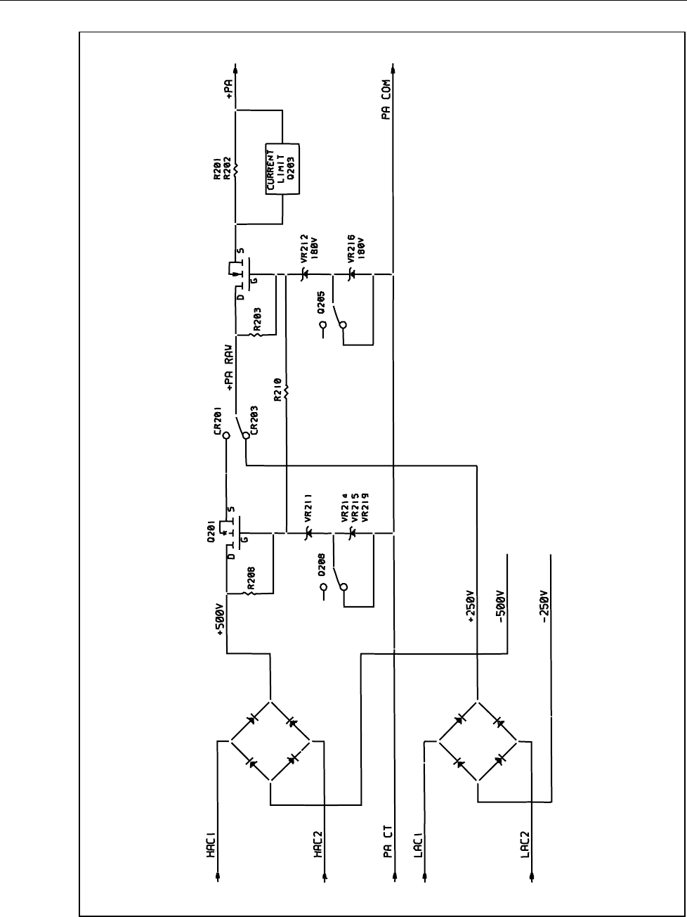
5700A/5720A Series II Calibrator
Service Manual
2-36
ahp005f.eps
Figure 2-6. Power Amplifier Output Supply Simplified Schematic

Theory of Operation
Analog Section Detailed Circuit Description
2
2-37
2-67. ±250V and ±500V Supplies
Input signals PA CT, PA HAC1, PA HAC2, PA LAC1, and PA LAC2 come from the
main transformer.
• PA CT is the center tap.
• PA HAC1 and PA HAC2 are high voltage taps with approximately 400V rms and
are fused by F201 and F204 respectively.
• PA LAC1 and PA LAC2 are lower voltage taps with approximately 200V rms and
are fused by F202 and F203 respectively.
• PA LAC1 and PA LAC2 and bridge rectifier CR222 generate the unregulated ±250V
supplies.
• PA HAC1 and PA HAC2 and diodes CR217, CR218, CR220, CR221, CR223,
CR224, CR227, and CR228 are in a bridge rectifier configuration to generate the
unregulated ±500V supplies.
When the PA supply outputs ±185V, current is drawn only from the lower voltage taps
LAC1 and LAC2.
2-68. +PA and -PA Supplies
Unregulated voltage for +PA is selected between the +250V and +500V unregulated
supplies by control line +HI/LO V and diodes CR201, CR203, CR208, and CR210.
Transistor Q204 is a current source that biases VR212 and VR216.
Supply +PA is +185V when the +HI/LO V signal is above 3V. (Transistors Q205 and
Q208 are turned on.) Transistor Q205 shorts VR216, while Q208 places a short across
VR214, VR215, and VR219. A voltage of +185V appears at the gate of Q202 because of
VR212. Approximately 140V appears at the gate of Q201. This 140V and about 250V at
the anode of CR208 reverse biases CR201 and CR210, thereby shutting off Q201.
Current flows out of the 250V unregulated supply through CR203 and Q202. Regulated
supply voltage +PA is determined by the gate voltage of Q202, which is about 190V
when +HI/LO V is above 3V.
When +HI/LO V is close to 0V, both Q208 and Q205 are turned off, and over 400V
appears at the gate of Q201. CR203 and CR208 are reverse biased, and the supply
current flows from the +500V unregulated supply through Q201, CR201, and Q202. The
gate voltage of Q202 is approximately 370V, nearly the same as +PA.
The -PA side works exactly like the +PA side except -PA is switched between -185V
and -365V by control line -HI/LO V.
The ±PA supplies can be replaced by the ±44SR unregulated supplies by moving switch
S201 switched towards the top edge of the board. This feature provides the means to
troubleshoot the Power Amplifier using reduced voltages.
NOTE
Make sure S201 is returned to the ±PA position before resuming normal
operation.
2-69. ±PA Supply Current Limit
The current limit for both the +PA and -PA supplies is set to either about 90 mA (K201
de-energized) or 150 mA (K201 energized) by K201. Control line +LO/HI I controls
relay K201. The high-current mode (150 mA) is used during operation in the 1100V dc
range and the 2.2A range.

5700A/5720A Series II Calibrator
Service Manual
2-38
Output current on the +PA side is sensed between the emitter and base of Q203 by R202
and/or R201. Supply +PA shuts off to near 0V when enough current is flowing through
+PA to forward-bias Q203. Then, current though Q203 charges capacitor C209 through
R214 to a voltage above the threshold voltage at the inverting input of comparator
U201C. The overcurrent condition must persist for about 75 ms for C209 to charge
above the threshold. The output of U201 goes high, turning on Q207. This forces the
zener diode bias current to flow through Q207 instead of VR212 or VR216, leaving only
a few volts at the gate of Q202, thus shutting +PA off. The output of U201C also
saturates Q218 and reduces the comparator threshold voltage to near 0V. This provides
the comparator with hysteresis; C209 has to discharge close to 0V before +PA can turn
on again. The +PA supply cycles on and off as long as the overcurrent condition exists.
Transistor Q206 provides another current limit. While otherwise similar to the Q203
limit, the Q206 current limit turns on at 0.5A and turns off immediately without any
delay. The Q206 limit thereby protects the supply under short circuit conditions.
Current limiting on the -PA side works similarly to the +PA side with one difference.
That is that shutoff of -PA can happen under two circumstances:
• -PA is loaded beyond its current limit.
• +PA is shut off. (Shut off of -PA is slaved to shut off of +PA.)
2-70. Regulator/Guard Crossing Assembly (A17)
The Regulator/Guard Crossing assembly (A17) provides two separate functions: voltage
regulation for the analog power supplies, and digital control of the guard crossing. The
voltage regulation portion is described first followed by the digital control portion. Refer
to the schematic diagrams for the Regulator/Guard Crossing Assembly for this
discussion.
2-71. Voltage Regulator Circuitry
The regulator circuit receives unregulated dc from the regulator filter circuit on the
Filter/PA Supply assembly (A18) and provides 13 regulated dc outputs and 1
unregulated dc output for the various analog assemblies. Table 2-10 lists the regulated
supplies from the Regulator/Guard Crossing Assembly.
2-72. Regulated OSC Supplies
The +15 OSC and -15 OSC supplies are used exclusively by the Oscillator Output (A12)
and Oscillator Control (A13) assemblies. OSC COM is the return path for these supplies.
The +15 OSC uses the unregulated +15 OSCR from the Filter assembly and consists of
three-terminal TO-220 regulator U2 with heat sink, bypass capacitors C1 and C2, and
protection diodes CR2 and CR3. The -15 OSC uses the unregulated -15 OSCR from the
Filter assembly and consists of three-terminal TO-220 regulator U3 with heat sink,
bypass capacitors C4 and C5, and protection diodes CR5 and CR7. Capacitors C2 and
C5 improve the stability of U2 and U3 respectively. Diodes CR3 and CR5 protect U2
and U3 from reverse voltages. Diodes CR2 and CR7 protect U2 and U3 from input
shorts.
Theory of Operation
Analog Section Detailed Circuit Description
2
2-39
Table 2-10. Regulated Outputs from the Regulator/Guard Crossing Assembly
Signal Name Nominal
Output Tolerance Current
Limit Rated
Output Test Point
+15 OSC +15V +/-800 mV 2A 200 mA TP3
-15 OSC -15V +/-800 mV 2A 200 mA TP5
+5RLH +5.975V +/-425 mV 2A 600 mA TP14
+5LH +5.1V +/-300 mV 2A 600 mA TP11
-5LH -5V +/-300 mV 2A 400 mA TP15
+44S +44.15V +/-2.03V 0.5A 140 mA TP13
-44S -44.15V +/-2.03V 0.5A 140 mA TP16
+17S +17.000V +/-475 mV 4A 1.0A TP8
-17S -17.000V +/-835 mV 6A 1.0A TP12
15S -15V +/-800 mV 2A 300 mA TP19
+30FR1 +30.96V +/-1.7V 1A 85 mA TP2
+30FR2 +30.96V +/-1.7V 1A 85 mA TP7
2-73. Regulated LH Supplies
LH COM is the return path for the +5RLH, +5LH, -5LH and +8RLH supplies. The
+5RLH, +8RLH, and +5LH supplies use the unregulated +5LHR supply from the Filter
assembly. The +5RLH supply uses three-terminal TO-3 regulator U11 with heat sink,
bypass capacitors C20 and C21, protection diodes CR17 and CR20, and the diode
combination of CR34 and CR35. The +5LH supply uses three-terminal TO-3 regulator
U8 with heat sink, bypass capacitor C16, protection diodes CR14 and CR16, and resistor
R13. The -5LH supply uses the unregulated -5LHR from the Filter assembly and consists
of three-terminal TO-220 regulator U12 with heat sink, bypass capacitors C23 and C24,
and protection diodes CR21 and CR24. Capacitors C16, C21, and C24 improve the
stability of U8, U11, and U12 respectively. Diodes CR14, CR17, and CR24 protect the
regulators from input shorts. Diodes CR16, CR20, and CR21 protect the regulators from
reverse voltage. Resistor R13 and diodes CR34 and CR35 increase the output of
regulators U8 and U11. The unregulated +8RLH supply is generated by fusing the
unregulated +5LHR supply from the Filter assembly with 3.15A slow-blow fuse F1.
2-74. Regulated S Supplies
Line S COM is the return path for the +44S, -44S, +17S, -17S, +15S and -15S supplies.
Line S COM is also connected to LH COM. The +44S supply uses the unregulated
+44SR from the Filter assembly. This supply uses three-terminal TO-39 regulator U10,
Q2, VR3, VR4, VR5, R20, R14, R15, CR18, CR19, CR25, C17, C18, C19, C65, PTC
resistor R60. The regulator IC (U10) provides the current and thermal limiting. Its
regulated output voltage is set by R14 and R15, yielding a nominal output of +44.15V.
Components Q2, R20, VR3 and VR4 act as an emitter follower to protect the regulator
against a potentially excessive input-output voltage differential in the event of a short
circuit. Capacitor C65 filters this voltage to the regulator. Diodes CR19 and CR25
protect the regulator against shorts at the input, while CR18 protects the regulated output
from reverse voltage. Capacitors C17 and C18 are for bypass. Capacitor C19 improves
rejection of input variations. Components U10 and Q2 have heat sinks to provide
thermal protection for both normal and short-circuit conditions. The regulator is shunted
by R60 and VR5, which normally pass 28 mA of current to remove the power from the
regulator. In an output short condition, the value of the PTC increases, limiting current
through the device to less than 17 mA at 25ºC.

5700A/5720A Series II Calibrator
Service Manual
2-40
The -44S supply uses the unregulated -44SR supply from the Filter assembly. This
supply uses three-terminal TO-39 regulator U13, Q1, VR1, VR2, VR6, R17, R18, R19,
PTC Resistor R61, CR22, CR23, CR32, CR33, C22, C25, C26, and C66. The regulator
IC, U13, provides the current and thermal limiting. Its regulated output voltage is set by
R17 and R18, yielding a nominal output of -44.15V. Components Q1, R19, VR1, VR2
and CR32 act as an emitter follower and protect the regulator against a potentially
excessive input-output voltage differential if a short circuit occurs. Capacitor C66 filters
the voltage to the regulator. The regulator is shunted by R61 and VR6, which pass 28
mA. In an output short condition, the value of the PTC increases, limiting current
through the device to less than 17 mA at 25ºC.
Diode CR32 removes VR2 from the circuit in a shorted condition to meet U13's input-
output differential specifications. Diodes CR22 and CR33 protect the regulator against
shorts at the output, while CR23 protects the regulated output from reverse voltage.
Capacitors C25 and C26 are for bypass. Capacitor C22 improves rejection of any input
variations. The heat sink on regulator U13 guarantees thermal protection for both normal
and short-circuit operating conditions.
The +17S supply uses the unregulated +17SR supply from the Filter assembly. This
supply uses three-terminal TO-3 regulator U6 with heat sink, and R5 and R6. The output
voltage is set by resistors R5 and R6 in the same manner as the +44S supply. Capacitors
C8 and C9 are for bypass. Capacitor C11 improves ripple rejection. Diodes CR8 and
CR26 protect the regulator against shorts at the input, while CR11 protects the regulated
output from reverse voltage.
The -17S supply uses the unregulated -17SR supply from the Filter assembly. It uses
three-terminal TO-3 regulator U7 and R10 and R11. The output voltage is set by
resistors R10 and R11 in the same manner as the -44S supply. Capacitors C13 and C15
are for bypass. Capacitor C14 improves ripple rejection. Diodes CR15 and CR27 protect
the regulator against shorts at the input, while CR13 protects the regulated output from
reverse voltage.
The +15S supply uses the unregulated +17SR supply from the Filter assembly. It
consists of +15V three-terminal TO-220 regulator U4. Capacitor C27 is required for the
stability of U4. Diode CR28 protects the regulator against shorts at the input, while
CR29 protects the regulated output from reverse voltage.
The -15S supply uses the unregulated -17SR supply from the Filter assembly. It consists
of -15V three-terminal TO-220 regulator U9. Capacitor C29 stabilizes U9. Diode CR31
protects the regulator against shorts at the output, while CR30 protects the regulated
output from reverse voltage.
2-75. FR1 Supply
FR1 COM is the return path for the +30FR1 supply. This supply uses the unregulated
+30FR1R supply from the Filter assembly and consists of three-terminal TO-39
regulator U1 with heat sink, bypass capacitors C3 and C6 and protection diodes CR1,
CR4, and CR6. Resistors R1 and R2 set the output voltage in the same manner as the
+44S supply. Capacitor C7 improves ripple rejection. Diodes CR1 and CR4 protect U1
against input shorts, while CR6 protects against reverse voltage.
2-76. FR2 Supply
FR2 COM is the return path for the +30FR2 supply. This supply uses the unregulated
+30FR2R supply from the filter assembly and consists of three-terminal TO-39 regulator
U5 with heat sink, bypass capacitors C10 and C28, and protection diodes CR9, CR10,
and CR12. Resistors R4 and R8 set the output voltage in the same manner as the +44S

Theory of Operation
Analog Section Detailed Circuit Description
2
2-41
supply. Capacitor C12 improves ripple rejection. Diodes CR9 and CR10 protect U5
against input shorts, while CR12 protects against reverse voltage.
2-77. Guarded Digital Control Circuitry
The Inguard CPU controls all the analog assemblies. It communicates with the
Unguarded CPU assembly (A20) through a serial fiber-optic link. The Inguard CPU is a
Hitachi 637A01Y0 CMOS microcontroller (U56) with 16K x 8 bit (16 KB, or 16
kilobyte) internal CMOS EPROM. Support circuitry includes 8K x 8 bits (8 KB) of
external CMOS static RAM, watchdog timer circuitry, reset and power glitch detect
circuitry, test switches, a serial fiber-optic link to the unguarded CPU, and decoders and
buffers to interface to the guarded digital bus. The assembly also generates an 8 MHz
sine wave for use by some of the analog assemblies.
2-78. Inguard CPU Memory Map
Table 2-11 shows the memory map of the Inguard processor.
Table 2-11. Inguard CPU Memory Map
Address Space (Hex) Name Use
0000 - 0027 Internal Registers on the 6301
0028 - 003F Unused memory space
0040 - 013F Internal RAM 256 Bytes
0140 - 3FFF CS0* Unused memory space
4000 - 4007 CS1* Wideband Output (A5)
4008 - 400F CS2* Current/Hi-Res (A7)
4010 - 4017 CS3* Switch Matrix (A8)
4018 - 401F CS4* Ohms Cal (A9)
4020 - 4027 CS5* Unused
4028 - 402F CS6 DAC (A11)
4030 - 4037 CS7* DAC (A11)
4038 - 403F CS8* Current/Hi-Res (A7)
4040 - 4047 CS9* Oscillator Control (A12)
4048 - 404F CS10* Oscillator Output (A13)
4050 - 4057 CS11* High Voltage Control (A14)
4058 - 405F CS12* Power Amplifier (A16)
4060 - 4067 CS13* Rear Panel (A21) Boost
4068 - 406F CS14* Current/Hi-Res (A7)
4070 - 4077 CS15* Wideband Oscillator (A6) Unused
4078 - 407F Unused
4080 - 5FFF Unused(memory overlay of 4000-407F)
6000 - 9FFF Unused
A000 - BFFF External RAM
C000 - FFFF Internal ROM or EPROM
2-79. Inguard Memory Configuration
The microcontroller (U56) has 16 KB (kilobytes) of internal EPROM program memory.
IC U62 provides 8 KB of external static CMOS RAM, with a jumper option for a plug-in
replacement with a 2 KB device.

5700A/5720A Series II Calibrator
Service Manual
2-42
2-80. Inguard Clock Circuit
This circuit uses 8 MHz crystal Y52 and step-down transformer T51 to generate a low-
level (200 mV p-p) 8 MHz clock used by other guarded assemblies throughout the
calibrator. Transformer (T51) has a center-tapped secondary, and provides CLK COM,
CLK and CLK*. The CLK and CLK* sine-wave signals are sent to certain analog
assemblies where they are converted into square wave clock signals for timing purposes.
2-81. Inguard Watchdog Timer
The watchdog timer circuit uses a 74HC4020 (U59) and part of Programmable Logic
Device (PLD) U58. The microcontroller (U56) generates a 19.2 kHz square wave
(SCLK) on pin 11. The frequency of this clock is the same as the baud rate of the serial
interface. Once the clock frequency is initialized, it runs without software supervision.
This clock drives U59, which divides by 16384 to obtain a logic low interval of 427 ms
followed by a logic high interval of 427 ms. The output of the U59, POPIN, goes to the
PLD, which asserts POP to the analog hardware and NMIPOP* to the processor if U59 is
not reset every 427 ms. The PLD also asserts POP on power-up and on any hardware
reset. In order to prevent POP and NMIPOP*, the watchdog counter must be reset by
reading or writing any analog hardware, or by toggling the POPCLRL line. The
POPCLRL line is also used to disable the watchdog by going low.
2-82. Power-Up and Reset Circuitry
This circuit consists of U60, SW51, C55, C56, R52, and Z51. The line monitor chip
(U60) detects three events: the power supply falling below 4.5V, reset being initiated by
closure of momentary contact switch SW51, or BREAK being asserted from the break
detection circuitry. If any of these conditions occurs, U60 resets the board for 130 ms.
Pin 5 of U60 is an open-collector output, pulled high by pin 12 of Z51.
2-83. Break Detection
The break-detect circuit acts as a serial communications break detector enabling the CPU
assembly (A20) to reset U56 and U58 via the power-up and reset circuitry. This break-
detect circuit uses a 74HC4020 binary counter (U63) and an inverter U51C. The
microcontroller (U56) outputs the 1.2288 MHz ECLK clock on pin 64. This signal
clocks U63, which in turn divides the signal by 16,384 to produce successive logic low
and high intervals (each of 6.67 ms) at the BREAK output (U63, pin 3). Under normal
conditions the RCV (receive) line is high to hold U63 clear. The main 68HC000 CPU
can force a reset of the Guard Crossing over the fiber-optic link by holding RCV low for
more than 6.67 ms, which causes BREAK to go high. BREAK, inverted by U51C, is
used by the reset circuitry to force a Guard Crossing reset via RESET*.
2-84. Fiber-Optic Link to CPU
Guarded digital and analog circuits are isolated from the unguarded CPU assembly
(A20) by a fiber-optic link that asynchronously transmits serial data. On the transmit
side, the microcontroller transmit output (XMT) controls a 75451 (U57) which drives
fiber-optic transmitter J72 mounted on the Analog Motherboard. Receive signal RCV
comes from fiber-optic receiver J71 also mounted on the Analog Motherboard. The
receiver converts the light signal to TTL levels that become the RCV signal at the
microcontroller. A fiber-optic cable links the fiber-optic transmitter on the Analog
Motherboard to the fiber-optic receiver on the Digital Motherboard. Another fiber-optic
cable links the other receiver/transmitter pair on the motherboards.

Theory of Operation
Analog Section Detailed Circuit Description
2
2-43
2-85. Interface to Guarded Digital Bus
The interface to the guarded digital bus consists of a 74HCT245 (U55), a 74HCT244
(U52), two 74HC137s (U53 and U54), inverters U51B and U51D, resistor packs Z52,
Z53, and Z54, and the POP line from U58. U52A and U52B buffer various control and
address lines. Resistors from Z52 pull the lines of U52A to desired inactive states when
BUSEN* is at a logic high, disabling the bus. U55 is a bi-directional data bus buffer
(D0-D7). Resistor packs Z53 and Z54 match the lines of the buffered data bus, reducing
reflected noise. ICs U53, U54, and U51D perform a 4-to-16 decode of address lines A3-
A6, generating 16 chip-select lines (CS0*-CS15*) on the guarded digital bus. These 16
signals select the various assemblies on the Analog Motherboard. U51B buffers and
inverts the INT interrupt signal from the DAC assembly. The POP signal from U58 is a
reset line sent to the analog assemblies.
2-86. Inguard CPU Interrupts
The Inguard CPU microprocessor handles many different interrupts. These are listed in
Table 2-12 in order of priority with the highest priority interrupts first.
Table 2-12. Inguard CPU Interrupts
Vector
MSB LSB Interrupt Description
FFFE FFFF *RES Power Up Reset
FFEE FFEF TRAP Address error or op code error
FFFC FFFD !NMI Non maskable interrupt (NMIPOPL)
FFFA FFFB SWI UNUSED
FFF8 FFF9 !IRQ1 !IRQ1,ISF (A/DINTL)
FFF6 FFF7 ICI Timer 1 input capture (unused)
FFF4 FFF5 0CI Timer 1 output compare 1,2 (unused)
FFF2 FFF3 TOI Timer 1 overflow (unused)
FFEC FFED CMI Timer 2 counter match
FFEA FFEB !IRQ2 UNUSED
FFF0 FFF1 SIO RDRF + ORFE + TDRE + PER
RDRF = Receive Data Register Full
ORFE = Overrun Framing Error
TDRE = TRANSMIT DATA REGISTER EMPTY
PER = Parity Error
2-87. Switch Matrix Assembly (A8)
Refer to Figure 2-7 for a simplified schematic of the Switch Matrix assembly (A8). The
Switch Matrix assembly does the following tasks:
• Coordinates the flow of signals from each analog assembly (excepting the Wideband
AC Module (Option -03)) to the calibrator’s binding posts. This communication
determines the calibrator’s range.
• Coordinates the connection of various analog and digital common lines during
operate, standby, and calibration modes.
• Controls such binding post functions as operate/standby, internal/external sense, and
internal/external guard.
• Provides an internal cal zero amplifier used in the calibration of offsets for all dcv
ranges (except the 1100V range).

5700A/5720A Series II Calibrator
Service Manual
2-44
The Switch Matrix assembly consists of 33 latching type, two- and four-pole relays. The
relays are driven by special driver chips, which are controlled by the assembly’s 24-
output 82C55 chip. The Switch Matrix also contains the 5700A-4HR1 Temperature-
Controlled Precision DC Amplifier Hybrid and RNET assembly, which is used when the
calibrator is in the dc 2.2V or 220 mV range. The resistor network also is used to create
resistive dividers to generate the ac or dc 220 mV, ac 22 mV, and ac 2 mV ranges.
Additional analog circuitry in the Switch Matrix Assembly includes the dc 2.2V range
output stage, the internal cal zero amplifier, FETs to support assembly calibration,
assembly diagnostics, and circuitry to control some of the motherboard relays.
2-88. Switch Matrix Digital Control
Refer to sheet four of the Switch Matrix schematic diagram for the following discussion.
The heart of the Switch Matrix digital control circuitry is an 82C55 Programmable
Peripheral Interface IC (U1) under software control via the guarded digital bus. This IC
has three ports that generate 24 outputs. These outputs are used to control eight
UCN5801 Latching Driver ICs (U5-U12) controlling all Switch Matrix latching relays,
one UCN5801 Latching Driver (U13) controlling the 10 non-latching relays on the
motherboard, a 4028 decoder (U2), five FET switches (Q6-Q7, Q9-Q11), and an analog
multiplexer (U4) for self diagnostics.
Eight UCN5801 latching driver ICs (U5-U12) drive Switch Matrix latching relays. Port
A (PA0-PA7) from U1 provides a common input bus. Each driver chip has a separate
strobe line. A 4028 decoder (U2) generates strobe lines U5STB-U13STB for strobing
U5-U13 respectively. These individual strobe lines are decoded from PB0-PB3 of U1.
When a strobe line is selected, the data on the bus is strobed in the respective driver chip.
The output enables are controlled directly by PC0-PC3 of U1. One bit of port C enables
two drivers. PC0 enables U5 and U6, PC1 enables U7 and U8, PC2 enables U9 and U10,
and PC3 enables U11 and U12. By enabling only two driver ICs at a time, excessive
power supply current draw is prevented. To ensure that the relays are latched properly,
the driver chips must be enabled for 10 ms. As an example, the following steps are taken
to set up relays in the first bank:
1. Write the proper data for the relays associated with driver U5 (K2,K9, K11, and
K15) to port A of the 82C55.
2. Write 0 hex to PB0-PB3 to make U5STB go high. Now write 9 hex toPB0-PB3 to
make all strobe lines go low. The data has now been strobed into U5.
3. Write the proper data for the relays associated with U6 (K3, K4, K5, and K24) to
port A of the 82C55.
4. Write 1 hex to PB0-PB3 to make U6STB go high. Now write 9 hex toPB0-PB3 to
make all strobe lines go low. The data has now been strobed into U6.
5. Write FE hex to port C (PC0 is low), wait 10 ms and write FF hex to port C. This
takes the outputs of U5 and U6 out of tri-state and allows the proper relay coils to be
energized for 10 ms.
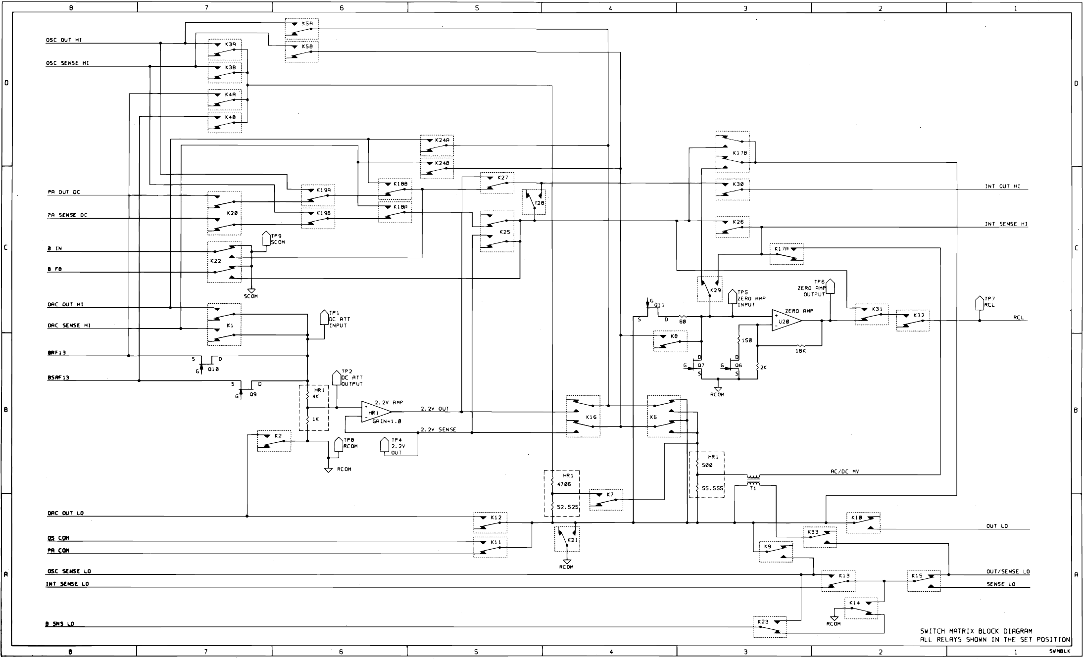
2
Theory of Operation
2-45
System Interconnection Detailed Circuit Description
Figure 2-7. Switch Matrix Assembly Simplified Schematic
ahp37f.eps

5700A/5720A Series II Calibrator
Service Manual
2-46
A UCN5801 driver (U13) drives non-latching relays on the motherboard. The
motherboard non-latching relay supply circuit, as outlined in sections A6 through A8 of
the schematic diagram, contains U17, Q1, Q2, CR1, CR2, CR10, and R6-R12. Port A of
U1 provides data for this driver (PA0-PA7), and decoder U2 provides the strobe signal.
Since this driver controls non-latching relays, the enable is tied to LH COM.
The non-latching relay supply circuit provides approximately 7V to the relays on the
motherboard during pull-in, and approximately 3.5V during normal operation. This
voltage is routed to the motherboard on the RLY+V line. The 7V is needed to ensure
pull-in while the 3.5V is sufficient to prevent drop out. This cuts relay heating and
thermal EMFs. PC5 controls the non-inverting amplifier U17. This amplifier is the
control element for Transistor Q1. When PC5 is low, the output is 3.5V, and when PB5
is high, the output is 7V. Components CR1, Q2 and R10-12 form a fold back current
limit for the supply. The following steps are taken to select a particular state for
Motherboard relays RLY1-RLY10:
1. Write the data corresponding to the desired state to port A(PA0-PA7) of the 82C55
(U1).
2. Strobe the data into U13 by writing 8 hex to PB0-PB3 to make U13STB go high,
then a 9 hex to make it go low.
3. Apply 7V to the relay coils by setting PC5 high.
4. Wait approximately 20 ms for the relays to pull in, then reduce the coil voltage to
3.5V by setting PC5 low.
There are five FETs on the Switch Matrix. Q9 and Q10 (sheet 3, C7), which are N-
channel JFETs controlled by port B (PB5) of U1, are driven by an LM393 open-collector
comparator (U15A) to provide the proper level shifting. DMOS enhancement FETs are
used for the remaining three FETs (Q6, Q7, and Q11). Refer to sheet 1, B5 of the
schematic diagram. FETs Q6 and Q7 are driven by U1, port B, with a high on PB4
turning on Q6, and a logic high on PB7 turning on Q7. FET Q11 is driven on by a logic
high from U1, port C (PC4).
The diagnostic circuit (sheet 4, B7) enables the calibrator to monitor +8RLH, the 2.2V
range output voltage, +5RLH, -5LH, +17S, -17S, the assembly temperature (U3), and the
OVEN TEMP line from the heated hybrid. OVEN TEMP, +5RLH, -5LH, and +8RLH
are divided down by a factor of 11 by Z5 and Z6. A 4051 analog multiplexer (U4) is
controlled by PA0-PA2 and PC6 from U1. This multiplexer selects which one of these
eight voltages is applied to the SDL line, where it is measured by the adc circuit on the
DAC assembly (A11).
2-89. Switch Matrix Operation
:
11V DC and 22V DC Ranges
Refer to Figure 2-8 for the following discussion. DC 11V and 22V ranges are generated
by the DAC assembly and routed directly to the front panel binding posts through relays
on the Switch Matrix and Motherboard.
Line DAC HI is connected to INT OUT HI through relays K18B, K27, and K30. INT
OUT HI is connected to the OUTPUT HI binding post through relay K1 on the
motherboard. Line DAC SENSE HI is connected to INT SENSE HI through relays
K18A, K25, and K26. Motherboard relays K2 and K3 switch INT SENSE HI to the
SENSE HI binding post during external sensing, or OUTPUT/SENSE HI during internal
sensing.
Lines PA COM and DAC LO are connected by relays K11 and K12, and connected to
the OUTPUT LO binding post by relay K10. Switch Matrix relays K14 and K15 connect
R COM to the SENSE LO binding post during external sensing, or to OUTPUT/SENSE
LO during internal sensing.
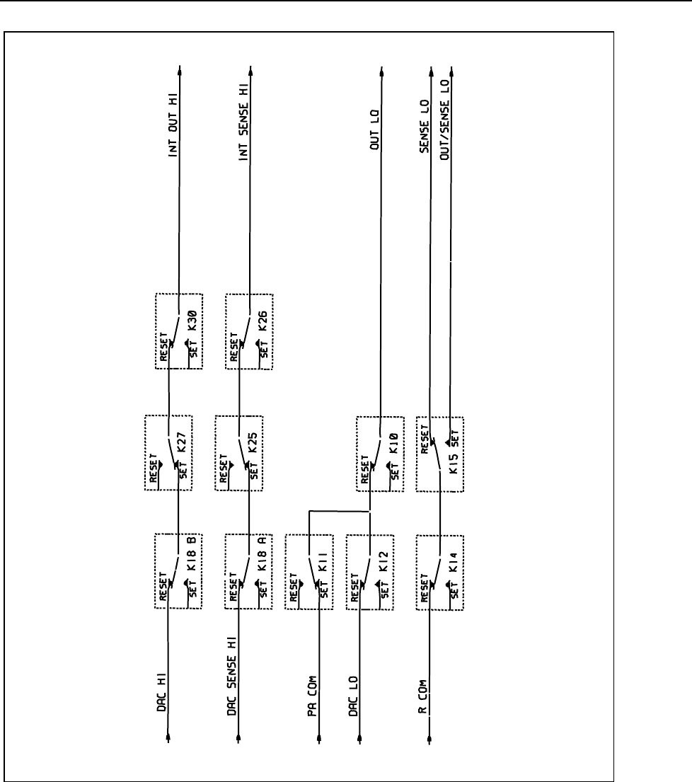
Theory of Operation
Analog Section Detailed Circuit Description
2
2-47
ahp006f.eps
Figure 2-8. Switch Matrix Configuration for 11V DC and 22V DC Ranges

5700A/5720A Series II Calibrator
Service Manual
2-48
2-90. Switch Matrix Operation
:
2
.
2V AC and 22V AC Ranges
Refer to Figure 2-9 for the following discussion. AC 2.2V and 22V ranges are generated
by the Oscillator assemblies and routed directly to the front panel binding posts through
relays located on the Switch Matrix and Motherboard.
Line OSC OUT is connected to INT OUT HI through relays K19A, K18B, K27, and
K30. INT OUT HI is connected to the OUTPUT HI binding post through relay K1 on the
motherboard. Line OSC SENSE is connected to INT SENSE HI through relays K19B,
K18A, K25, and K26. Motherboard relays K2 and K3 switch INT SENSE HI to the
SENSE HI binding post during external sensing, or OUTPUT/SENSE HI during internal
sensing.
Line OSC COM is connected to the OUTPUT LO binding post through relays K11 and
K10 on the Switch Matrix. Switch Matrix relays K13 and K15 connect OSC SENSE LO
to the SENSE LO binding post during external sensing, or OUTPUT/SENSE LO during
internal sensing.
2-91. Switch Matrix Operation
:
220V AC and DC Ranges
Refer to Figure 2-10 for the following discussion. In the dc 220V range, PA OUT HI
from the Power Amplifier assembly (A16) is routed to the High Voltage Control
assembly (A14), where it goes through relay K10 and becomes PA OUT DC. Line PA
OUT DC is routed to the Switch Matrix and connected to INT OUT HI through relays
K20, K19A, K18B, K27 and K30. Relay K1 on the motherboard connects INT OUT HI
to the OUTPUT HI binding post.
Line PA SENSE DC is connected to INT SENSE HI through relays K20, K19B, K18A,
K25, and K26. Motherboard relays K2 and K3 switch INT SENSE HI to the SENSE HI
binding post during external sensing, or OUT/SENSE HI during internal sensing. PA
COM and DAC LO are connected by relays K11 and K12, and connected to the
OUTPUT LO binding post by relay K10. Switch Matrix relays K14 and K15 connect R
COM to the SENSE LO binding post during external sensing, or OUTPUT/SENSE LO
during internal sensing.
In the ac 220V range, Power Amplifier outputs PA OUT HI and PA SNS AC are routed
to the High Voltage Control assembly (A14) where relays K10, K3, and K13 connect
them to HV OUT and HV SNS respectively. HV OUT is connected to the OUTPUT HI
binding post through relays K9 and K1 on the motherboard. Motherboard relays K10,
K2, and K3 connect HV SNS to the SENSE HI binding post during external sensing, or
to OUTPUT/SENSE HI during internal sensing. Connection to the OUTPUT LO and
SENSE LO binding posts is done with relays on the Switch Matrix. PA COM is
connected to the OUTPUT LO binding post through relays K11 and K10. Switch Matrix
Relays K13 and K15 connected OSC SENSE LO to the SENSE LO binding post during
external sensing, or OUTPUT/SENSE LO during internal sensing.
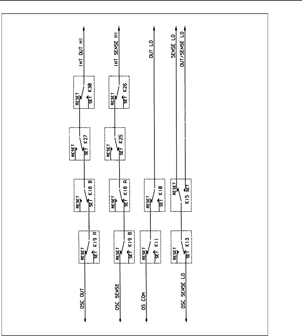
Theory of Operation
Analog Section Detailed Circuit Description
2
2-49
ahp007f.eps
Figure 2-9. Switch Matrix Configuration for 2.2V and 22V AC Ranges
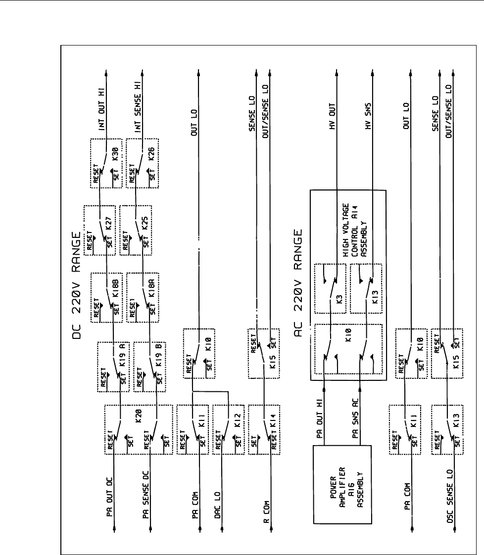
5700A/5720A Series II Calibrator
Service Manual
2-50
ahp008f.eps
Figure 2-10. Switch Matrix Configuration for 220V DC and AC Ranges

Theory of Operation
Analog Section Detailed Circuit Description
2
2-51
2-92. Switch Matrix Operation
:
2
.
2V DC Range
Refer to Figure 2-11 for the following discussion. The dc 2.2V range circuit consists of
the dc 2.2V attenuator and a dc 2.2V range amplifier as outlined on sheet 3 of the Switch
Matrix schematic. This circuit contains a CA3096 transistor array IC (U19A-E),
transistor Q4, FETs Q12 and Q13, resistors R20, R23-R30, and R32, relays K1 and K2,
part of the resistor network 4R07, and a dc amplifier heated hybrid.
The resistor network is bonded to the hybrid and this entire assembly is called the
5700A-4HR1 (HR1) on the schematic. Transistor Q3 drives the heater resistor on the
hybrid. The heater control circuit adjusts the base voltage of Q3 to deliver the correct
power to the heater resistor to maintain thermal control. Transistor Q8 protects the
hybrid in case Q3 fails.
To produce the dc 2.2V range, the DAC assembly (A11) is set to the 11V range. DAC
OUT HI and DAC SENSE HI are connected to pin 10 of the resistor network by relay
K1, and DAC LO is connected to pin 9 by relay K2. The network divides the voltage by
five. The divided voltage from pin 8 is connected to the input (pin 11) of the dc amplifier
hybrid.
This temperature-controlled amplifier is used as a buffer amplifier. The output of the
buffer amplifier (pin 18) drives the 2.2V range high current output stage consisting of
U19, Q4, R25-R30, R32, and CR7-CR9. This circuit enables the 2.2V range to support
50 mA of current with current limiting. FETs Q12 and Q13 provide localized feedback
for the precision dc amplifier during unusual conditions, such as a short circuit at the
OUTPUT binding posts or when this range is in standby.
Line 2.2V OUT is connected to INT OUT HI through relays K27 and K30 on the Switch
Matrix. Line INT OUT HI is connected to the OUTPUT HI binding post through relay
K1 on the motherboard. Line 2.2V SENSE is connected to INT SENSE HI through
relays K25 and K26 on the Switch Matrix. Motherboard relays K2 and K3 switch INT
SENSE HI to the SENSE HI binding post during external sensing, or to
OUTPUT/SENSE HI during internal sensing.
Line PA COM is connected to the OUTPUT LO binding post through relays K11 and
K10. Switch Matrix relays K14 and K15 connect R COM to the SENSE LO binding post
during external sensing, or OUTPUT/SENSE LO during internal sensing.
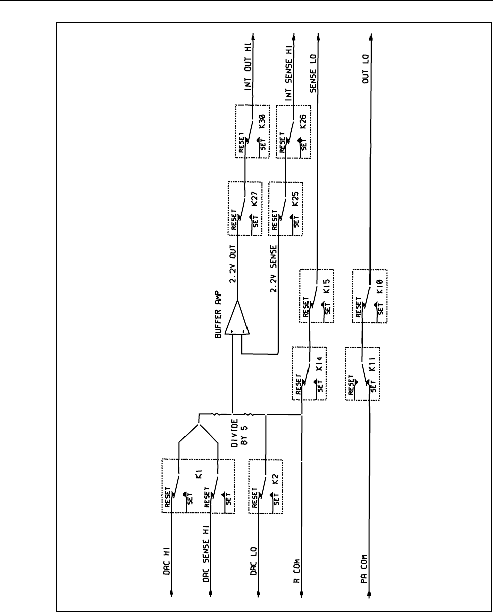
5700A/5720A Series II Calibrator
Service Manual
2-52
ahp009f.eps
Figure 2-11. Switch Matrix Configuration for 2.2V DC Range

Theory of Operation
Analog Section Detailed Circuit Description
2
2-53
2-93. Calibration of the 2
.
2V Range
Refer to Figure 2-12 for the following discussion. Calibration of the 2.2V range involves
determining its offset and gain constants.
To calibrate the offset:
1. The gain of the internal cal zero amplifier is set to 130 by turning on Q6 via PB4.
2. A checkpoint reading is taken, which represents 0V at the input of the internal call
zero amplifier. In this configuration, PBS turns on FET Q7 connecting RCOM to the
internal cal zero amplifier input, K29 is open (set position), and the output of the cal
zero amplifier is connected to RCL via relays K31 and K32.
3. The input of the internal cal zero amplifier is connected to the output of the 2.2V
range. The 2.2V range is adjusted until the adc reads the same as the checkpoint
reading within the given tolerance. In this configuration, 2.2V OUT and 2.2V
SENSE are tied together by relay K28 and the output (NIT SENSE HI) of the range
is channeled into the internal cal zero amplifier input (sheet 1) through relay K29.
To calibrate the gain of the 2.2V range, the 13V buffered reference (BRF13 and
BSRF13) from the DAC assembly (A11) is connected to the input of the 2.2V range by
FETs Q9 and Q10 on sheet 3 of the schematic. Since this network divides the voltage by
five, a voltage of 2.6V is obtained at the 2.2V OUT and 2.2V SENSE points. These
points are tied together by relay K28. This voltage is then channeled to the RCL line by
relays K31 and K32 where it is connected to the +input of the adc amplifier on the DAC
assembly (A11). The DAC output is connected to the -input of the adc amplifier and is
adjusted until a null is achieved. At this point, the DAC voltage represents the output
voltage of the 2.2V range. Gain is determined since the output, input, and offset of the
2.2V range are now known.
2-94. Switch Matrix Operation
:
220 mV DC Range
Refer to Figure 2-13 for the following discussion. The 220 mV range is an extension of
the dc 2.2V range. The 2.2V range is divided by ten to produce the 220 mV range. This
10:1 divider (on sheet 2 of the Switch Matrix Schematic) is part of the resistor network
on the 4HR1 assembly.
The 220 mV range is passive with an output resistance of 50Ω. This range is generated
by connecting the 2.2V OUT and 2.2V SENSE to pin 3 of the 10:1 divider by relays K16
and K6. Lines PA COM and R COM are connected to pin 2 of the 10:1 divider by relays
K11 and K21. This divided output from pin 1 is called AC/DC mV on the schematic.
This portion of the resistive attenuator is also used for generating the ac 2.2 mV and 22
mV ranges. The AC/DC mV signal is then connected to INT SENSE HI through relay
K17A on sheet 1 of the Switch Matrix schematic. Line INT SENSE HI is connected to
the OUTPUT HI binding post through relays K2 and K3 on the motherboard. Sensing for
the LO occurs by connecting R COM and PA COM via K11 and K21. A single line is
run out to the OUTPUT LO binding post by relay K33 on the Switch Matrix.
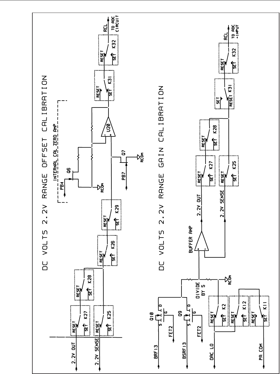
5700A/5720A Series II Calibrator
Service Manual
2-54
ahp010f.eps
Figure 2-12. Calibration of the 2.2V DC Range
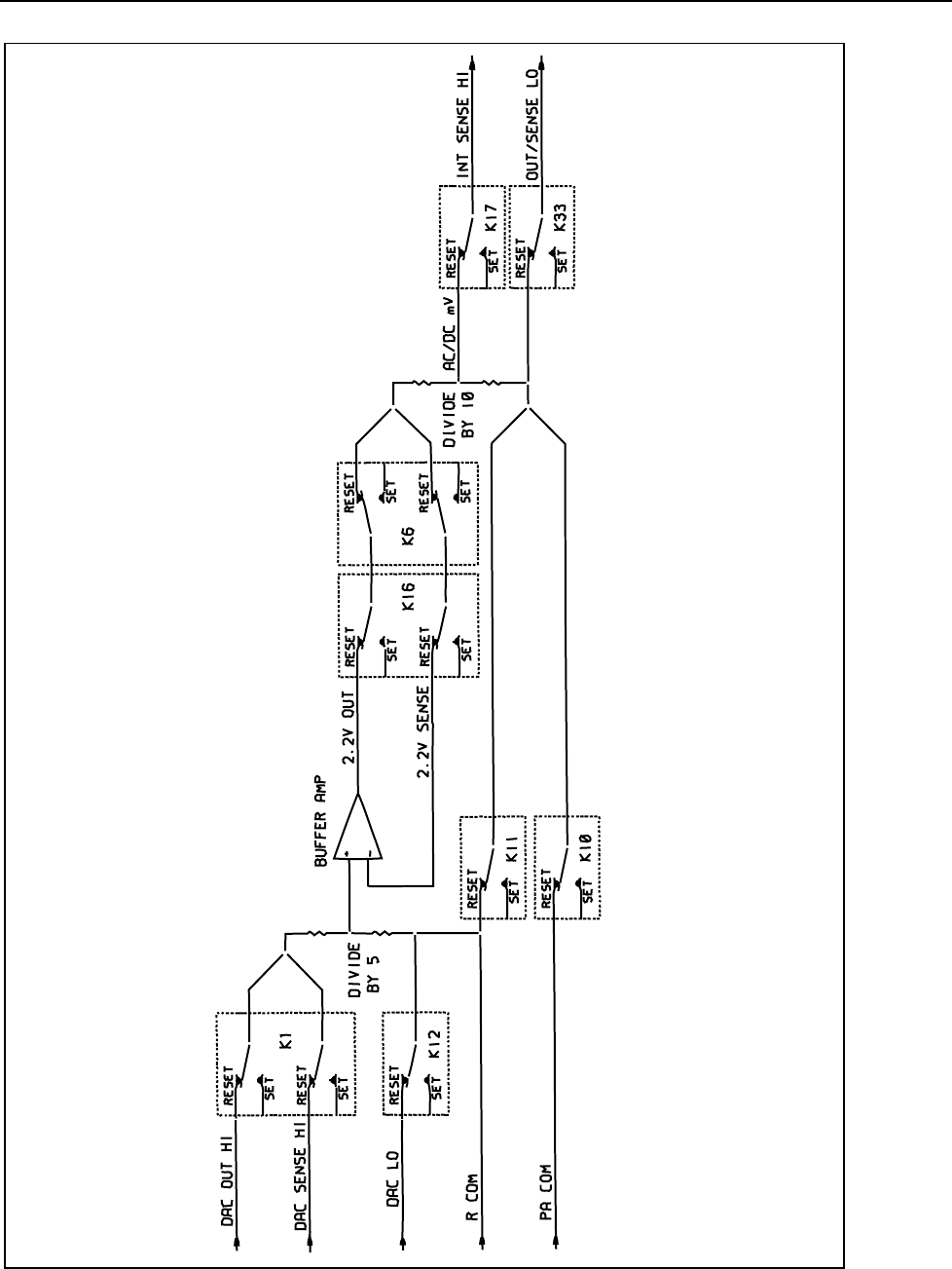
Theory of Operation
Analog Section Detailed Circuit Description
2
2-55
ahp011f.eps
Figure 2-13. Switch Matrix Configuration for 220 mV DC Range

5700A/5720A Series II Calibrator
Service Manual
2-56
2-95. Switch Matrix Operation
:
220 mV AC Range
Refer to Figure 2-14 for the following discussion. As previously mentioned, the ac 220
mV range uses the same resistor network as the dc 220 mV range. In generating the ac
220 mV range the Oscillator assembly is set to the 2.2V range. Lines OSC OUT and
OSC SENSE are connected to pin 3 of the 10:1 divider by relays K5 and K6. Lines OS
COM and OSC SENSE LO are connected to pin 2 by relays K11 and K9 respectively.
This divided output from pin 1 is referred to as AC/DC mV on the schematic. The
AC/DC mV is then connected to INT SENSE HI through relay K17 on sheet 1 of the
Switch Matrix schematic. Signal INT SENSE HI is connected to the OUTPUT HI
binding post through relays K2 and K3 on the motherboard. Sensing for the LO occurs
by connecting OS COM and OSC SENSE LO via K11 and K9. A single line is run out to
the OUTPUT LO binding post by relay K33 on the Switch Matrix.
2-96. Switch Matrix Operation
:
2
.
2 mV and 22 mV AC Ranges
Refer to Figure 2-14 for the following discussion. The ac 2.2 mV and 22 mV ranges use
the 100:1 divider and the 10:1 divider of resistor network on 4HR1 for a total division of
1000:1. Switch Matrix operation for these two ranges is the same. For the 2.2 mV range,
the Oscillator assembly is set to the 2.2V range. For the 22 mV range, the Oscillator
assembly is set to the 22V range.
Signals OS COM and OSC SENSE LO are connected to pin 6 of the 100:1 divider and
pin 2 of the 10:1 divider by relays K11 and K9. OSC OUT and OSC SENSE are
connected to the input (pin 7) of the 100:1 divider by relay K3 (A and B). The output of
this 100:1 divider is then connected to the input of the 10:1 divider (pin 3) by relay K7.
At the output of the 10:1 divider (called AC/DC mV on the schematic) there is a total
division of 1000:1. Connection to the binding posts is done in the same manner as in the
ac 220 mV range. In all cases, the output impedance of the millivolt ranges is 50Ω.
2-97. Calibration of the mV Ranges
Calibration of the mV ranges involves determining the resistor ratios of the 10:1 divider
and the 1000:1 divider (100:1 and 10:1 dividers cascaded). In addition, an offset
calibration is performed on the 10:1 divider to remove thermal EMF error for the 220
mV dc range.
Refer to Figure 2-15 for the following discussion. The 10:1 divider offset is calibrated by
configuring the Switch Matrix for the 220 mV dc range, except with the output of the
range (AC/DC mV) switched into the input of the internal cal amplifier through relays
K17 and K29. The Calibration procedure is the same as described for the 2.2V range
offset calibration except that during a checkpoint reading, control line PC4 turns on Q11
which connects SWM SENSE LO to the input of the zero amplifier, representing 0V for
the 220 mV range.
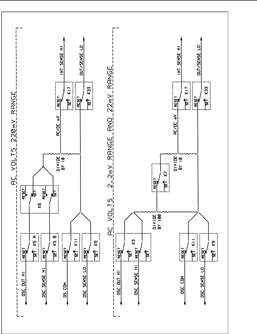
Theory of Operation
Analog Section Detailed Circuit Description
2
2-57
ahp012f.eps
Figure 2-14. V AC, 2.2 mV AC, and 22 mV AC Range
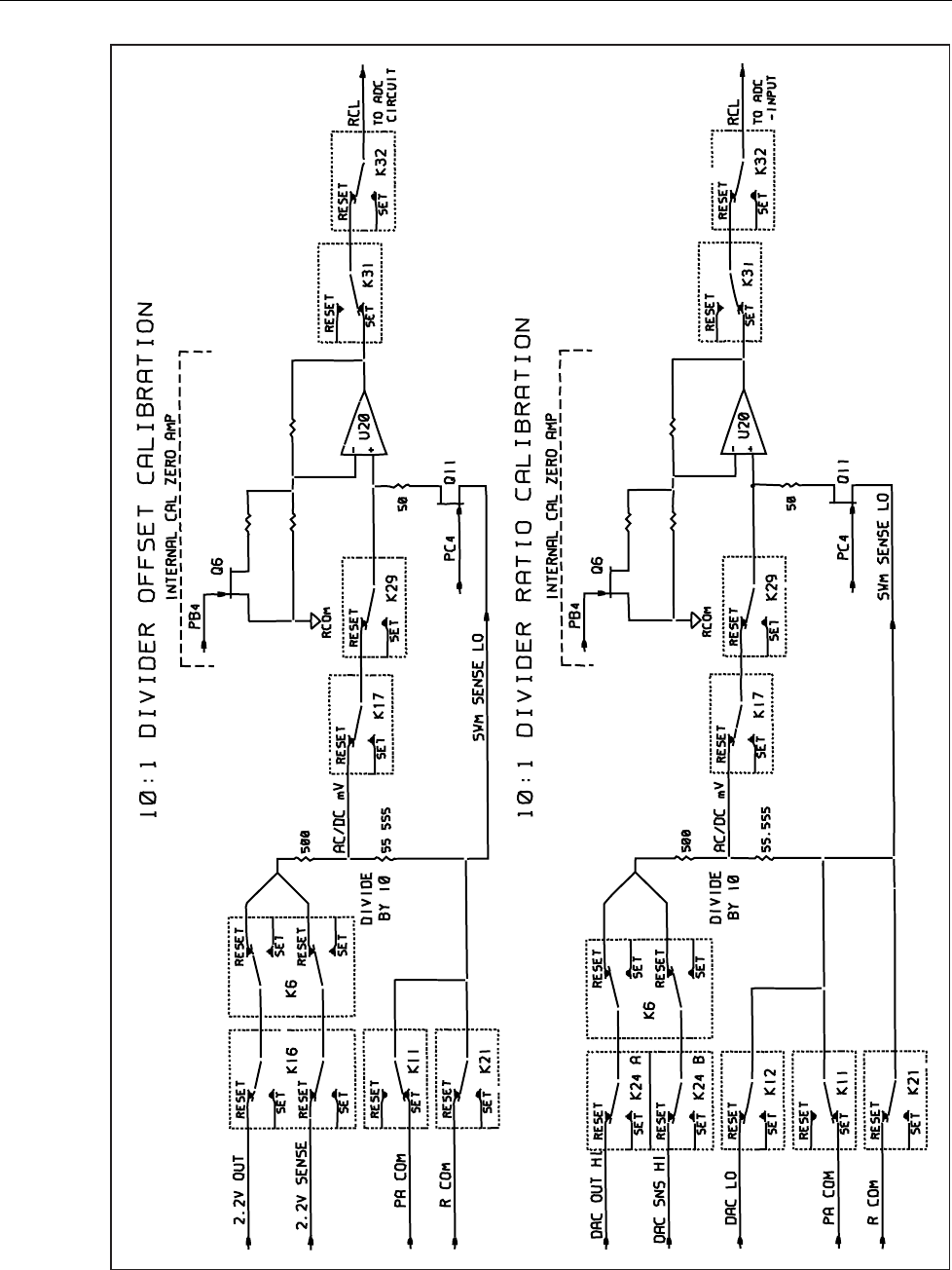
5700A/5720A Series II Calibrator
Service Manual
2-58
ahp013f.eps
Figure 2-15. Divider Calibration

Theory of Operation
Analog Section Detailed Circuit Description
2
2-59
Calibration of the 10:1 divider ratio is accomplished by connecting the DAC assembly
output (DAC OUT HI and DAC SENSE HI) through relays K24 (A and B) and K6 to the
input of the 10:1 divider. DAC LO, PA COM, and R COM are connected to the common
of the 10:1 divider by relays K12, K11, and K21 respectively. The DAC output is set to
2.2V to produce approximately 0.22V at the output of the 10:1 divider (AC/DC mV).
Relays K17 and K29 direct this voltage to the internal cal zero amplifier, which is
configured for a gain of 10, giving 2.2V plus an unknown error at its output.
The equation for this output is the DAC output (2.2V) multiplied by the 10:1 divider
ratio (unknown) multiplied by the internal cal zero amp gain (calibrated, approximately
10). Once the output of the internal cal zero amplifier is determined, the 10:1 divider
ratio is the only unknown, so it can be calculated.
To determine the output of the internal cal zero amplifier for this configuration, a
checkpoint reading is first taken by connecting both inputs of the DAC’s adc amplifier to
the DAC output, which is set to 2.2V. This reading represents a null at 2.2V. The output
of the internal cal zero amplifier is then channeled to the RCL line by relays K31 and
K32 and to the +input of the adc amplifier on the DAC assembly with the DAC output
still connected to the -input. An adc reading is now taken and the checkpoint reading is
subtracted from it. This value is the adc’s representation of the deviation of the internal
cal zero amplifier output from 2.2V.
However, due to inaccuracy in the adc, an additional step must be taken. The -input of
the adc amplifier is connected to RCOM and the +input to the DAC output. The DAC
output is adjusted until the adc reads the previous value within the given tolerance. At
this point, the DAC output voltage represents accurately the deviation of the internal cal
zero amplifier output from 2.2V. The output of the internal cal zero amplifier is now
calculated, allowing the 10:1 divider ratio to be determined.
Refer to Figure 2-16 for the following discussion. Calibration of the 100:1 divider ratio
is similar to calibration of the 10:1 divider ratio. The 13V buffered reference (BRF13
and BSRF13) is connected to the input of the 100:1 divider pin 7 by relay K4 (A and B).
DAC LO, PA COM , and R COM are connected to pin 6 of the 100:1 divider by relays
K12, K11, and K21 respectively. The voltage at the divider output (pin 5) is
approximately 0.13V. Relay K7 connects the output of the 100:1 divider to the input of
the 10:1 divider. Relays K6 and K8 connect it to the ac mV CAL line, which is the input
to the internal cal zero amplifier. The result is 1.3V at the amplifier output. This voltage
is switched onto the RCL line by relays K31 and K32 to the DAC assembly, where the
DAC is nulled to it. At this point, the DAC voltage represents the internal cal zero
amplifier output and the 100:1 divider ratio is calculated.
2-98. Internal CAL Zero Amplifier
The main function of the internal cal zero amplifier is to remove the offsets of each of
the dc ranges except the 1100V range. (The 1100V dc range is zeroed at the High
Voltage/High Current assembly.) The internal cal zero amplifier is switched into two
gain configurations for range zeroing; a gain of 130 for the 22V ranges and below, and a
gain of 10 for the 220V range. Each range is channeled into the internal cal zero
amplifier via relay K29. The range is then compared against 0V by connecting R COM
to the amplifier via FET Q7. For the 220 mV range, the reading for 0V (or checkpoint
reading) is taken by turning on Q11 instead of Q7 in order to achieve a 50Ω impedance.
The output of the amplifier is connected to the RCL line by relays K31 and K32, and
then channeled to the DAC assembly where the signal is measured by the adc.
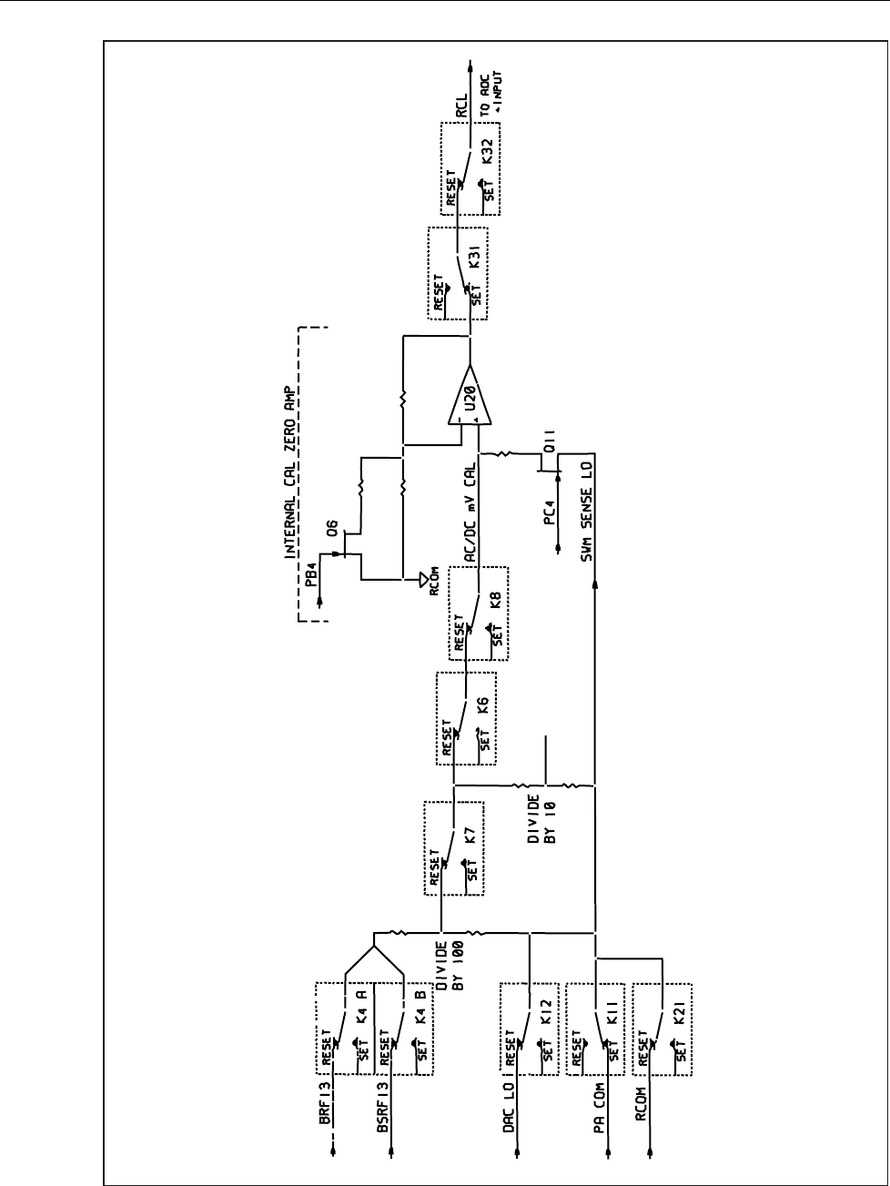
5700A/5720A Series II Calibrator
Service Manual
2-60
ahp014f.eps
Figure 2-16. Divider Gain Calibration

Theory of Operation
Analog Section Detailed Circuit Description
2
2-61
The internal cal zero amplifier is outlined in a broken line rectangle on sheet 1 of the
schematic. Its functional parts are U20-U21, R38-44, R46-47, Q6-7, Q11, and Z2. When
Q7 is on, the input of the zero amplifier is connected to 0V for a reference point. When
Q6 is on, the gain of the zero amplifier is 130. Op amp U21 and its associated resistors
form a current-cancellation circuit. It senses the output of the zero amplifier and creates
a current equal in magnitude but opposite in polarity to the current through the gain
resistors (Z2), resulting in zero current in the precision common (RCOM).
2-99. Switch Matrix 5725A Amplifier Interface
The Switch Matrix also provides switching between the calibrator and the 5725
Amplifier. The ac and dc input signals necessary to operate the 5725A are connected by
relay K22. Relay K23 connects B SNS LO to either OSC SENSE LO or R COM via
relay K14.
2-100. DAC Assembly (A11)
The DAC (digital-to-analog converter) is the basic building block of the calibrator. Other
assemblies create ac and dc voltages and currents with its precision dc voltage. The DAC
contains five assemblies:
• DAC Main Board (A11)
• DAC Filter SIP (A11A1)
• DAC Buffered Reference SIP (A11A2)
• Reference Hybrid (HR5)
• DC Amplifier Hybrid (HR6).
The DAC assembly serves two main functions:
• To provide a highly repeatable stable dc voltage
• To support calibration of the calibrator
The DAC’s adc circuit is used to accomplish calibration. It is made up of an analog to
digital converter (adc) and the adc amplifier. Together, these are used to completely
characterize the calibrator, using only one external voltage source and two external
resistor standards.
2-101. Basic DAC Theory of Operation.
Figure 2-17 is a simplified schematic of the DAC assembly. The DAC uses a pulse-
width-modulated scheme to produce a precision dc voltage of 0V to 22V with positive
and negative polarity. The DAC contains:
• A 13V temperature-controlled reference hybrid (HR5)
• Duty-cycle control circuitry
• A five-pole active filter (A11A1 assembly)
• An output stage
• Digital control circuitry
• These basic subcircuits work together for a stable and linear dc voltage.
The DAC assembly also contains:
• A sense-cancellation circuit
• Linearity control circuits
• Negative offset circuit
• An output switching circuit
The two inputs of the five-pole filter are two precision square waves with different fixed
amplitudes and independently variable duty cycles controlled by software. The filter’s

5700A/5720A Series II Calibrator
Service Manual
2-62
first input square wave is called the first channel. It is switched between the reference
voltage (13V) and 0V.
The filter’s second input square wave is called the second channel. It is switched between
approximately 0.78 mV and 0V. Its amplitude is derived by resistively dividing the 13V
reference. This second channel is used for extra resolution.
The filter rejects all ac components of the waveforms above 10 Hz. Since the frequency
of the square waves is 190 Hz, the output of the filter is a dc voltage which is the sum of
average voltages of the two waveforms. The Output Stage, which consists of the dc
amplifier hybrid and the output buffer, isolates the filter output from the DAC output and
gives current drive to the DAC output.
The output stage has a current limit of approximately 60 mA. It can be configured for a
gain of one for the 11V range, or a gain of two for the 22V range. Relays on the DAC
output lines allows them to be inverted for negative polarity.
To change the DAC voltage, the average value of the two square waves must be varied.
To determine the average value, multiply the waveforms amplitude by its duty cycle.
Vary the duty cycle and keep the amplitude fixed to change the DAC voltage.
For example, if the duty cycle of the first channel is 10% and the second channel 50%,
the overall average voltage would be:
(0.1 x 13V) + (0.5 x 0.78 mV) = 1.300390V.
The duty cycle resolution is 0.0024%, which gives a first channel resolution of 0.309 mV
and second channel resolution of 18.5 nV.
The duty cycle control circuitry creates the two digital square waves for the first and
second channels. These two waveforms are first run through optocouplers for isolation
and then into analog switching and level shifting circuits. These circuits derive the
proper signals to switch the input of the filter at the levels explained above.
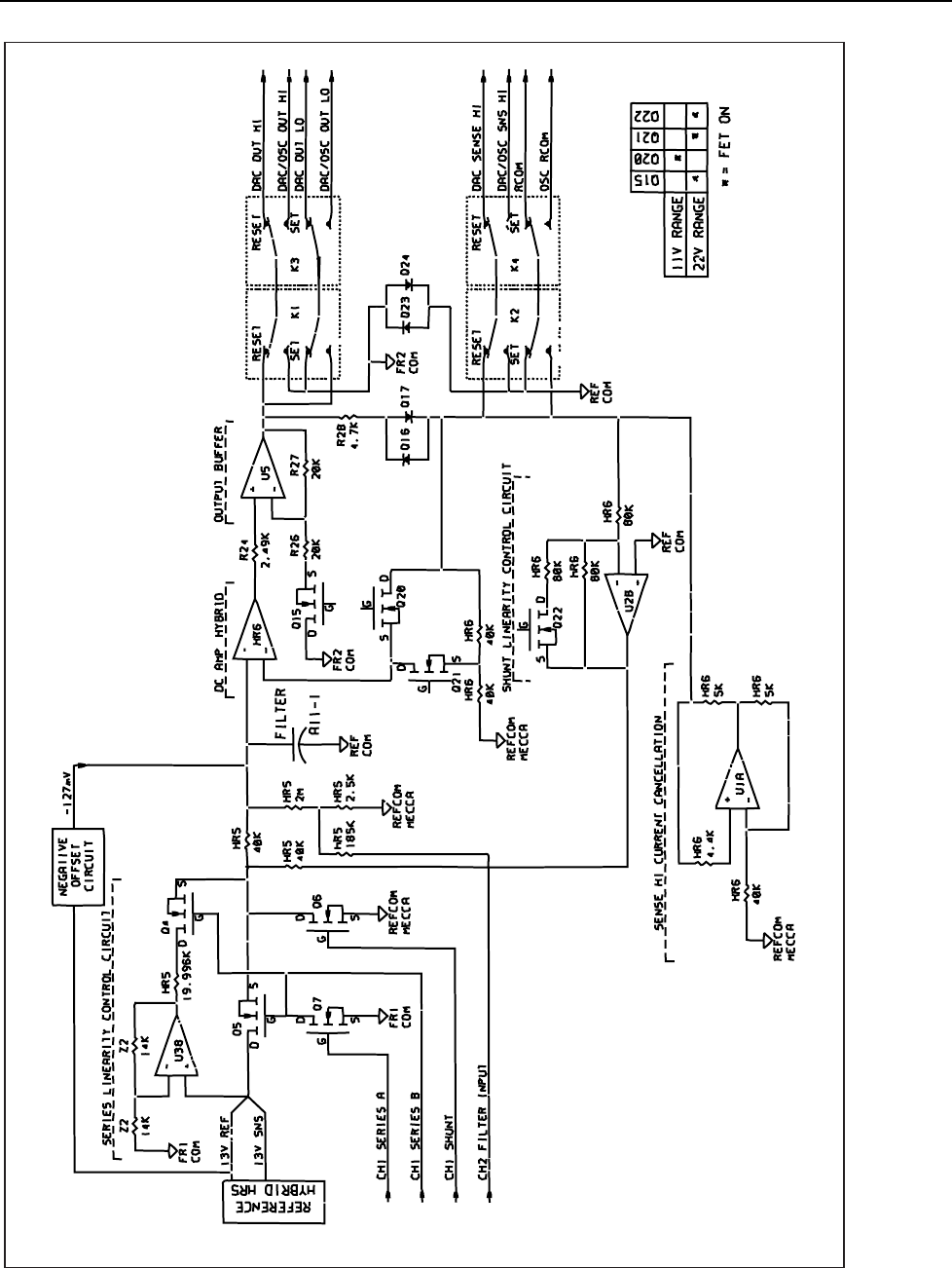
Theory of Operation
Analog Section Detailed Circuit Description
2
2-63
ahp015f.eps
Figure 2-17. DAC Assembly Simplified Schematic

5700A/5720A Series II Calibrator
Service Manual
2-64
2-102. DAC Assembly Digital Control
The digital control circuit is located on sheet 6 of the DAC schematic. The 82C55
Programmable Peripheral Interface IC (U31) is the heart of this circuit.
This IC, which is under software control via the guarded digital bus, has three ports that
provide 24 static lines. Port A (PA0-PA7) is configured as a read-only port register. It
passes the adc readings from the ADC IC (U25) to the guarded digital bus.
PB0-PB4 of port B control relays K1-K4 and K6-K8 via relay drivers U33 and U34. PB0
is also control line DAC OUT SEL used to turn on FET Q25, via FET Q26, and connect
RCOM to SCOM during calibrator operation in the ac function.
PC7 of port C, buffered by U8A, provides the enable for these relay drivers. Relay driver
U33 controls latching relays K7 and K8. Outputs from U33 are also used by Relay driver
U34 to control latching relays K1-K6. PB5-PB7 are decoded by U32 to create six control
lines. These control lines are used to select one input to the adc amplifier -input. K5SEL
is an input to the relay drivers to control latching relay K5. The remaining five control
lines are used by comparators in U35 and U36. These comparators provide the proper
level shifting to create control lines BSRF6 SEL, BSRF13 SEL, REF6 SEL, REF13 SEL,
and ADC COM SEL. These control lines are used to control FETs on the DAC Buffered
Reference SIP assembly (A11A2).
PC0 of port C is buffered by U8 (B and C) and routed through opto-isolator U37 to
create RANGE SELECT, which sets the DAC to the 11V or 22V range. PC1 is used in
the duty cycle control circuit to shut off the 8 MHz clock via buffer U8F and the first
channel via OR gate U9D. This is done during calibrator operation in the resistance
function. PC2 controls a FET in U23 for use in self-diagnostics. PC3 and PC4 are level-
shifted by comparators in U36 before they are used to control FETs in U23. PC5 of port
C is connected to a comparator in U36. This comparator provides the proper level
shifting to create control line ADCAMP OUT SEL to control a FET in U23. PC6 is
control line ADC TRIGGER which triggers the adc (analog-to-digital converter) IC U25.
A0, A1, and CS*, from the guarded digital bus, are used by OR gates in U9 (B and C) to
create control line ADC READ for use by the adc IC U25.
2-103. DAC Assembly Reference Circuitry
The reference circuitry is on the reference hybrid, located on the HR5 assembly. The
HR5 assembly contains a ceramic substrate reference hybrid bonded to a resistor
network.
All components on this assembly are surface mount devices, except U6 and U7. The
resistors are screened with a thick film paste. Associated resistors, capacitors, and zener
diodes are mounted on the main board to supply this hybrid with the appropriate power
and ground returns.
As previously explained, the amplitudes of the pulse width modulated signals for the
first and second channel are assumed to be fixed. Any change in amplitude shows up as
an error on the output of the DAC. Since the reference is used to determine the
amplitude, it must be very stable and generate little noise.
The 13V reference contains two cascaded 6.5V temperature compensated
transistor/zener diode pairs called ref amps (U6 and U7). The excellent temperature
characteristics of the ref amps are obtained by biasing the collector current on their
transistors with a value such that the TC (temperature coefficient) of its base-emitter
junction cancels the TC of the zener diode. Since the base-emitter junction and the zener
diode are in series, the result is a near zero TC.
Correct bias currents are achieved with a thin-film resistor network in a surface-mount
package mounted on the hybrid.

Theory of Operation
Analog Section Detailed Circuit Description
2
2-65
The reference circuit is designed such that the effects of the thin-film resistors and op
amp errors are second order. Thus, accuracy is determined almost entirely by the ref
amps.
To further reduce the effects of ambient temperature variations, the hybrid is heated to a
constant 62ºC by the heater control circuitry on sheet 1 of the DAC schematic.
Temperature is sensed near the ref amps by a thermistor (RT1). If the substrate
temperature changes, the thermistor resistance changes. This creates a correction voltage
to the base of Q2 (on the main board). This, in turn, causes the power into the heater
resistor, which is screened on the back of the substrate, to increase or decrease as
necessary to maintain a stable temperature.
Thermal runaway is prevented by a protection circuit. Once the substrate temperature
reaches approximately 67ºC, the change in resistance of RT2 causes Q9 to turn on. As
transistor Q9 turns on, it steals base current from Q1 on the main board, which brings it
out of saturation. This breaks the current path through the heater resistor. This condition
exists only if there is a failure.
The exact value of the reference is determined during calibration. Because of the
stability of the reference, it can be used for future internal calibration procedures to
remove short term errors in the calibrator.
The 13V output, REF13 HI, is from pin 9 and REF13 SENSE is on pin 12. Also, a 6.5V
reference line, REF6, is brought out on pin 14 of the reference for use during calibration.
In order to make these reference voltages available to other assemblies, the 6.5V and
13V references are buffered on the DAC Buffered Reference SIP assembly (A11A2).
This assembly also contains the circuitry to switch the references and buffered references
into the input of the adc during calibrator calibration. Refer to the section on the DAC
Buffered Reference SIP for more information.
2-104. Duty-Cycle Control Circuit
Duty-cycle control circuitry is pictured on sheet 3 of the schematics. DAC output
voltages are represented in software by what are called first and second channel counts.
Each count is a 16-bit number which is sent to the DAC assembly via the guarded digital
bus.
For example, a first channel count of 20,000 (in decimal) represents a DAC output
voltage of approximately 6.5V (half the reference voltage).
The first function of the duty-cycle control circuitry is to convert each count into a
stable, TTL level, square wave, with a duty cycle proportional to the numeric value of
the count. This is accomplished with the 82C54 programmable interval timer (U6).
A low-level 8 MHz clock is generated on the Regulator/Guard Crossing assembly (A17)
and routed to the DAC assembly via the motherboard. This low-level clock, CLK and
CLK*, is amplified to a TTL level by comparator U7 to generate the 8 MHz clock which
is used by U6 and the adc IC U25.
The 82C54 programmable interval timer receives its input counts from the guarded
digital bus and creates the second channel signal on OUT2 (pin 20) and the first channel
signal on OUT1 (pin 16).
The second channel signal is buffered by U8 (D and E) and runs through opto-isolator
U12 to become CH2 FLOATING. This signal alternately turns FETs Q30 and Q32 on
and off to turn the 3V source (called 3V) into a floating 3V pulse width modulated
waveform called CH2 FILTER INPUT.

5700A/5720A Series II Calibrator
Service Manual
2-66
The 3V source is created from the 13V reference. The 13V reference is buffered by op
amp U1B, configured as a voltage follower. The output from U1B is divided down to 3V
by a 100 kΩ and 30 kΩ resistor in the HR5 assembly, creating 3V.
This 3V is again buffered by op amp U11, configured as a voltage follower, to create the
3V, which is switched by FETs Q30 and Q32. CH2 FILTER INPUT uses three resistors
on the HR5 assembly to resistively divide its 3V amplitude by an additional factor of
approximately 3800.
The first channel signal is buffered by U8 (G and H) and run through opto-isolator U13,
to become CH1 FLOATING. Since the first channel is much more critical than the
second, CH1 FLOATING is clocked into a flip flop (U14) to ensure an accurate
waveform.
To clock in this waveform, the low-level 8 MHz clock (CLK and CLK*) from the
Regulator/Guard Crossing assembly (A17) is isolated by transformer T1 and amplified
to a TTL level by comparator U10. This generates the clock inputs for U14. The output
Q1 (pin 5) from U14 creates CH1 SERIES A, which switches Q7. The output Q1* (pin
6) is inverted by Q35, creating CH1 SHUNT, which switches Q6. The output Q1*, which
is a TTL level, is also amplified by components Q33, Q34, VR11, VR12, and R44-R46,
so it switches from 0 to 18V, creating CH1 SERIES B, which switches Q4 and Q5.
The watchdog timer sets the first channel filter input to 0V if a failure occurs on the 8
MHz clock. This circuit uses a monostable multivibrator (one shot) U15, C63, and R48.
The 8 MHz clock is divided to 4 MHz by U14. This 4 MHz clock is connected to U15
and discharges C63 to ground. If the 4 MHz clock stops, C63 charges up, causing the Q1
output of U15 to go low. This logic low on Q1 is connected to the preset pin of U14
(PRI), which causes its Q1 output high and its Q1* output low. This condition turns on
the shunt switch and turns off the series switch, which forces the filter input to be
REFCOM.
2-105. DAC Filter Circuit
The dac filter circuit is located on the DAC Filter SIP (A11A1) assembly. The dominant
pole of the filter is near 10 Hz. This gives 120 dB of rejection at 190 Hz.
The +30FR1 supply and 15V zener diode, VR1, create the 15V supply (15V) for the op
amps in the filter circuit. 15V is also connected to the main DAC board, where it is used
with R111 as a pull up for the RANGE SELECT control line.
2-106. DAC Output Stage
The output stage of the DAC assembly consists of the DC Amplifier Hybrid assembly
(HR6) and the output buffer circuitry. Like the Reference Hybrid, the DC Amplifier
Hybrid is constructed of surface-mount components (except precision op amp U2), on a
ceramic substrate hybrid, bonded to a resistor network.
It is temperature-controlled by a heater control circuit in the same manner as explained
on the Reference Hybrid. Transistor Q3 provides proper power to the heater resistor.
The DC Amplifier Hybrid consists of a precision op amp U2, with a bootstrapped power
supply (Q1, Q2, R1-R4, VR1-VR2). The op amp has low noise and low offset. It is
bootstrapped to improve the common-mode rejection in its noninverting configuration.
The DC Amplifier assembly interfaces with the output buffer (U5) to create the output
stage. Control line RANGE SELECT configures this output stage for unity gain for the
11V range or a gain of 2 for the 22V range. In the 11V range, Q15 is turned off, which
gives U5 unity gain, and Q20 is on, which gives the DC Amplifier unity gain.

Theory of Operation
Analog Section Detailed Circuit Description
2
2-67
In the 22V range, Q20 is off and Q21 is on, which switches in the 40 kΩ feedback
resistors located on the HR6 assembly. Precise ratio matching of these resistors provides
high accuracy in the 22V range.
FET Q15 is on in the 22V range so that the output of the dc amplifier is half the output
of the DAC. This is necessary so that the output of the dc amplifier is approximately the
same as its inputs, which allows the bootstrap circuit to work.
The output buffer (U5) provides drive for the DAC output. It is used in a feedback loop
with the DC Amplifier Hybrid so that the dc accuracy is dependent upon the dc
amplifier, and the output drive capability is dependent on the output buffer.
The output buffer is current-limited to a short circuit current of about 60 mA. The short-
circuit protection circuitry works as follows:
1. The supply current is sensed by R23. When the output current of U5 reaches
approximately 50 mA, the voltage across R23 is large enough to turn on Q10.
2. As Q10 turns on, the voltage across R20 increases, and pulls down the supply
voltage at pin 4 of U5.
3. In order to prevent the supply of U5 from dropping below the input, Q8 saturates
turning on Q11 which shorts the input to FR1 COM.
4. When the short is removed, R22 and C41 cause Q11 to turn off slowly, which
prevents a large overshoot at the DAC output.
2-107. Sense Current Cancellation Circuit
This circuit uses op amp U1A and four resistors on the HR6 assembly. This circuit
supplies the sense current of equal, but opposite, polarity to the feedback resistors in the
22V range. This eliminates current in the sense lead during external sensing.
2-108. Linearity Control Circuit
The linearity control circuitry contains the series linearity control circuit and the shunt
linearity control circuit, as outlined on the schematic. These linearity control circuits
eliminate filter current in the series switch (Q5) and the shunt switch (Q6). This is
necessary because Q5 and Q6 have finite resistance (3 to 5Ω) and a small mismatch in
the resistances can cause a linearity error.
The series linearity control circuit uses op amp U38, resistor network Z2, and a single
19.996 kΩ resistor on the HR5 assembly. This circuit eliminates filter current in the
series switch Q5.
When the series switch (FET Q5) is on, it connects the 13V reference to the first channel
input of the filter, and FET Q4 is also turned on. This causes U38 to supply the current to
the filter through the 19.996 kΩ resistor in HR5 and Q4, which makes the resistance
from TP2 to TP5 look like near 0 ohms.
The shunt linearity control circuit uses op amp U2B, FET Q22, three 80 kΩ resistors on
the HR6 assembly, and one resistor in the HR5 assembly.
Op amp U2B is configured as an amplifier with an inverting gain of 1 in the 11V range,
and an inverting gain of 0.5 in the 22V range. This gain is determined by FET Q22 and
the three 80 kΩ resistors in the HR6 assembly.
When the shunt switch (FET Q6) is on, connecting the input of the filter to REFCOM,
the current from the filter flows through the two 40 kΩ resistor (pin 7 to pin 8) on the
HR6 assembly to the output of U2B. This cancels out the current that would flow
through Q6 which makes it look like 0Ω.

5700A/5720A Series II Calibrator
Service Manual
2-68
2-109. Negative Offset Circuit
This circuit creates a constant offset voltage of approximately -127 mV at the filter
input. Thus, for a DAC output voltage of 0V, the first channel count must be
approximately 400 to offset this negative voltage. This guarantees a minimum duty cycle
pulse width of approximately 50 us.
This minimum duty cycle is necessary to overcome the offset of the output stage and to
allow the reference voltage to settle out after being switched into the filter input. Op amp
U2A and two 20 kΩ resistors in HR6 form an amplifier with an inverting gain of 1. This
amplifier input is the 13V reference which produces -13V at its output. This -13V is
divided by resistors in the HR5 assembly to create the -127 mV on the filter input.
2-110. DAC Output Switching
The floating outputs of the DAC are switched with latching-type relays K1, K2, K3, K4,
and K8.
Relays K1 and K2 determine the polarity of the DAC. In the reset position, the DAC
output is positive. In the set position, output is negative. Relay K1 also generates DAC
LO DIAG and DAC HI DIAG which are used by the adc circuit during DAC diagnostics.
Relays K3 and K4 switch the DAC to various assemblies. In the reset position, the DAC
is available to all assemblies except the oscillator. Relays K3 and K4 are set during
operation in the ac function so the DAC output is connected to the DAC/OSC lines
which run only to the Oscillator assembly. Also during operation in the ac function,
control line DAC OUT SEL turns on FET Q25, via FET Q26, to connect SCOM to
RCOM.
Relay K8, when in the set position, allows the DAC to be sensed right on the output of
the DAC assembly.
2-111. DAC Buffered Reference Sip
The DAC Buffered Reference SIP assembly (A11A2) has two main functions. First, it
buffers the 6.5V and 13V references so they can be used by other assemblies.
The 6.5V reference, REF6, is buffered by op amps U1A and U2A which creates BRF6
and its sense line BSRF6. The 13V reference, REF13 FILT, is buffered by op amps U1B
and U2B which creates BRF13 and its sense line BSRF13. These are routed to other
assemblies in the calibrator for use during calibrator calibration.
Second, it allows the reference voltages, or the buffered reference voltages, to be
switched to the REFCAL line, which is connected to the inverting input of the adc
amplifier by K5 during calibration of the DAC assembly.
Control line REF6 SEL and FETs Q1 and Q2 connect the 6.5V reference REF6 to
REFCAL.
Control line BSRF6 SEL and FETs Q5-Q7 tie BRF6 and BSRF6 together and connect
them to REFCAL.
Control line REF13 SEL and FETs Q8 and Q9 connect the 13V reference REF13 to
REFCAL.
Control line BSRF13 SEL and FETs Q12-Q14 tie BRF13 and BSRF13 together and
connect them to REFCAL.
ADC COM can also be connected to REFCAL by FET Q15 and control line ADC COM
SEL.

Theory of Operation
Analog Section Detailed Circuit Description
2
2-69
2-112. Calibration Hardware
The main components of the calibration hardware are the adc amplifier and the adc
(analog to digital converter). This adc circuitry converts dc analog voltages into 22-bit
binary numbers which the software interprets.
2-113. ADC Amplifier
ADC amplifier circuitry is located on sheet 4 of the DAC schematic. The adc amplifier is
used like a null detector. It has two inputs (inverting and noninverting) and a single
output with ADC AMP OUT and ADC AMP SENSE connected together.
The noninverting input (+INPUT) is switched between ADC COM, RCL, or DAC
SENSE CAL by relays K6 and K7. DAC SENSE CAL is the output of the DAC and
RCL is the calibration line which other assemblies use during their calibration.
The inverting input (-INPUT) is switched between DAC SENSE CAL and REFCAL by
relay K5. ADC amplifier inputs are high impedance. The output voltage is the voltage
difference between the inputs multiplied by the overall adc amplifier gain of 11.
To determine adc amplifier output, the following formula is used: (Noninverting input -
inverting input) x 11 = adc amplifier output. For example, if the noninverting input is a
5.0V and the inverting input is at 5.1V, the output would be -1.1V. (The calculation for
this example is (5.0V - 5.1V) x 11 = -1.1V.) Op amp U20A configured as an amplifier
with an inverting gain of 1 is used to cancel the current in ADC COM generated from op
amp U19A.
Zener diodes VR19 and VR20 keep the output of the adc amplifier from exceeding
±4.0V. Similarly, this protection is provided for the adc amplifier inputs by VR17,
VR18, VR21 and VR22.
2-114. ADC Input Selection
The input to the adc chip, U25, is selected by a quad FET analog switch array, U23. A
large filter (R74 and C84) and a buffer (U24) are put on the adc input line to filter out 60
Hz and 190 Hz before it is connected to the adc chip input (pin 22).
During calibrator diagnostics, control line PC2 selects the SDL (system diagnostic line)
line, which is used by other analog assemblies to monitor their diagnostic voltages.
During diagnostics of the DAC assembly control, line PC3 selects DAC HI DIAG which
is divided by R79 and R84. Control line PC4 selects DCAMP HEATER and REF
HEATER which are summed and divided by R80, R81, and R83.
Since DCAMP HEATER and REF HEATER are referenced to FR1 COM, DAC LO
DIAG is buffered by U22 to provide the proper current return.
During calibrator calibration, control line ADC OUT SEL selects the output of the adc
amplifier.

5700A/5720A Series II Calibrator
Service Manual
2-70
2-115. ADC Circuit
The adc (analog-to-digital converter) is shown on sheet 5 of the DAC schematic.
Most of the adc is contained on one chip (U25) which uses the Fluke-patented
recirculating remainder technique.
The adc has rms noise of approximately 20 µV between readings. This is reduced by a
factor of 5 by averaging the readings. The adc measures input voltages between -1.8V
and +1.8V.
Hardware for the adc has four major sections external to adc IC U25. These sections are:
• ADC reference voltage
• ADC dac
• ADC comparator/amplifier
• Timing/data control circuitry.
The adc reference voltage circuit is made up of zener diodes VR29, VR30, and resistors
R91-R93, which generate a 6.4V reference. This -6.4V is inverted by U27B to create the
+6.4V reference and is also buffered by U27A and connected to U25. A reference
common point for the adc reference is made by buffering ADC COM with op amps
U20B and U26A, resulting in an isolated ADC COM. Buffering allows the common
point to be referenced to ADC COM, yet current from R85, C89, C90, R93, VR29, and
VR30 to return to SCOM through the output of the buffer instead of through ADC COM.
The adc dac contains the dac amplifier, U28B, and a binary ladder network consisting of
resistors in Z10. Digitally controlled analog bit switches are contained in U25. The bit
switches determine the output voltage of U28B by control of the binary ladder network.
The output voltage of U28B can be varied from -1.95V to 1.95V.
The adc comparator/amplifier contains op amp U29, two remainder storage capacitors
(C89 and C90), an autozero storage capacitor (C95), and several digitally-controlled
analog switches in U25.
The supplies for U29 are bootstrapped off its input voltage. This circuitry includes
U28A, VR31-VR34, R95-R100, Q56, Q57, and C97.
The timing/data control circuit is the digital portion of U25. This internal circuitry
controls the adc by manipulating the switches in the adc comparator/amplifier and the bit
switches in the adc dac.
An adc conversion cycle is triggered by the falling edge of control line ADC TRIGGER
from the digital control circuit. Once triggered, the adc, under control by U25, generates
five 6-bit nibbles without any further interaction.
Once the adc is triggered, it goes through five measurement cycles. Each cycle is made
up of three functions, an autozero function, a compare function and a remainder store
function. Figure 2-18 illustrates these three functions.
Before the adc is triggered, it stays in the autozero function. In this function, the adc dac
is set to 0V with some offset error. Through U25, pin 3 of U29 is connected to ADC
COM and pins 2 and 6 are connected together. In this function, the offset of the adc dac
is stored on C95.
In the compare function, U29 compares the adc dac with the adc input (during the first
pass) or the stored remainder (C89 or C90) during the remaining four passes. The
voltage to be measured is switched into pin 3. The adc dac is connected to pin 2 and
adjusted according to the polarity output of U29 resolving the voltage on pin 3. During
this function the six bits of one nibble are determined.
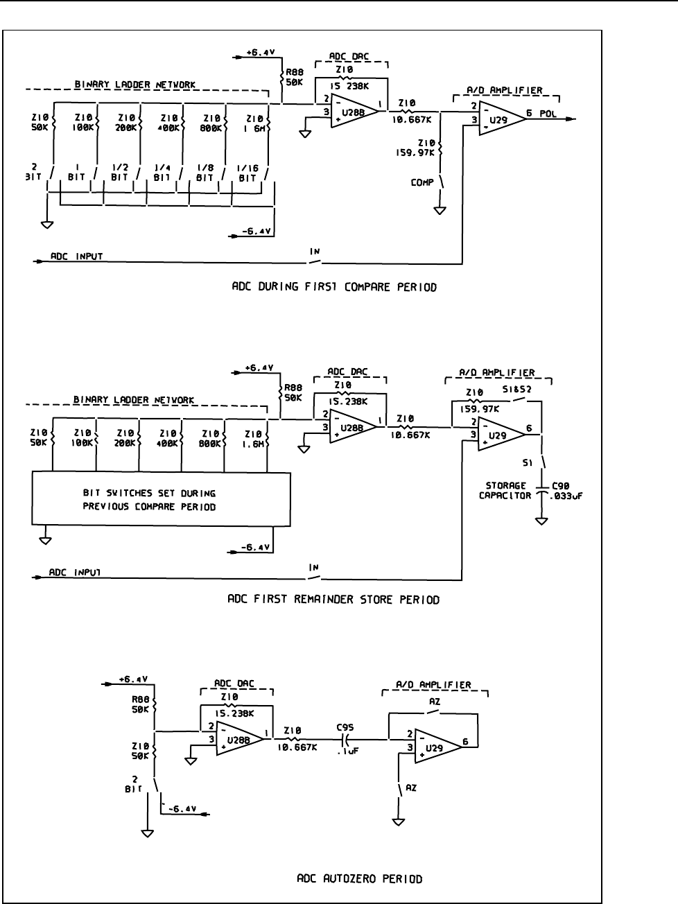
Theory of Operation
Analog Section Detailed Circuit Description
2
2-71
ahp016f.eps
Figure 2-18. ADC Circuit Measurement Functions

5700A/5720A Series II Calibrator
Service Manual
2-72
During the remainder store function, U29 amplifies and stores the difference between the
ADC INPUT and the adc dac output on one of the remainder storage capacitors, C89 or
C90. In this function, U29 is configured by the adc as a difference amplifier with a gain
of 16. The output of U29 is now the difference between the input voltage and the DAC
voltage, multiplied by 16. This voltage is stored on C89 or C90.
On the next cycle, this remainder voltage is switched into U29 as the input voltage
during the compare function.
Once this is repeated five times, U25 sends out an interrupt signal (ADC INT) to tell the
processor that it is waiting to read. To read the five passes of the adc, the processor reads
port A of the 82C55 five times.
For the most critical applications, the adc measures the output of the adc amplifier. Since
the output of the adc amplifier is adjusted until it reaches a checkpoint voltage, the adc
needs only to be repeatable at this voltage and low in noise. This reduces the constraints
on adc linearity and long term stability which allows a much simpler adc reference to be
used.
2-116. How the DAC is Used in Calibration
For internal and external calibration, the adc amplifier output is switched to ADC
INPUT.
The adc amplifier acts as a null meter. It measures the voltage difference between its
inverting and noninverting inputs and amplifies it by a gain of 11.
The adc amplifier can measure common-mode voltages up to 14V. Input switching
circuitry allows the DAC SENSE, buffered and unbuffered reference, RCL, and ADC
COM to be switched into the adc amplifier inputs.
To make a typical cal measurement, software sets the DAC to the approximate expected
common-mode voltage. The DAC is then switched into both adc amplifier inputs and an
adc reading is taken. This is the checkpoint measurement. It represents the adc amplifier
common-mode and offset error, and the errors in the adc and adc amplifier input
switching. The unknown voltage is switched into one input of the adc amplifier and the
DAC is adjusted by software until the adc reading matches the checkpoint reading. At
this point the unknown voltage is equal to the DAC voltage and is represented by the
current DAC counts.
2-117. DAC Assembly Calibration
The DAC assembly is completely characterized using a single external 10V source.
Calibration occurs in the following steps:
Ratio calibration of the first and second channels is performed first. The first channel
count is set for a DAC output of near 0V. The second channel count is set to its
minimum value of approximately 10,000. The DAC output is connected to the input of
the zero amplifier on the Switch Matrix assembly (A8) and its output connected to the
+input of the adc amplifier via the RCL line and the -input is connected to ADC COM.
The adc measures this value and stores it as a checkpoint reading. The first channel is
decremented by one count and the second channel is increased until the adc reads the
same as the previous checkpoint. The number of counts the second channel is increased
represents the channel ratio constant.
The ±11V and ±22V range zeros are calibrated next. This is done by the same technique
as the ratio cal except the checkpoint reading is obtained by connecting the input of the
zero amplifier on the Switch Matrix assembly to RCOM. The DAC output (DAC SENSE
CAL) is then connected to the zero amplifier input and adjusted until the adc reads the

Theory of Operation
Analog Section Detailed Circuit Description
2
2-73
same as the previous checkpoint. This determines the exact first and second channel
counts for a 0V output.
Next, the +11V and +22V range gain constants are calibrated by nulling the DAC to the
external 10V source, connected to the front panel binding posts of the calibrator. This
10V source is connected to the RCL line by relays on the Switch Matrix assembly (A8).
The RCL line is connected to the +INPUT of the adc amplifier. The DAC output is
connected to the -INPUT of the adc amplifier and is adjusted until the adc reads a null.
This determines the first and second channel counts required for an exact 10 V output
from the DAC. Software determines floating point gain constants from these counts.
The exact value of all the reference voltages (6.5V and 13V) are determined next. The
reference voltage to be determined is connected to the -INPUT of the adc amplifier. The
DAC output is connected to the +INPUT and adjusted until the adc reads a null. The
reference voltage is the value to which the DAC is set. This procedure is done for the
6.5V buffered and unbuffered, and 13V buffered and unbuffered references.
2-118. Oscillator Section Overview
The ac module consists of two plug-in assemblies, the Oscillator Output assembly (A13)
and the Oscillator Control assembly (A12). These assemblies generate a precision
amplitude-stabilized ac sine wave from 0.22V to 22V with a frequency range of 10 Hz to
1.2 MHz. This signal is either routed to the OUTPUT binding posts if the desired output
is within this range, or used internally by the Power Amplifier, High Voltage, Wideband,
Current, Switch Matrix, or an Auxiliary Amplifier (Model 5725A), for voltages and/or
functions outside this range.
Output sensing of the amplitude helps obtain an accurate output signal regardless of
output amplitude and load variations. Sensing is available for all voltage ranges above
200 mV at the calibrator SENSE binding posts. In the current function, and for voltages
less than 200 mV, sensing is performed internally and output accuracy is guaranteed
only for specified operating conditions.
The Oscillator Output assembly (A13) creates an ac voltage. The Oscillator Control
assembly (A12) controls the amplitude of this ac signal by comparing the SENSE HI
signal from the Oscillator Output with an accurate dc voltage from the DAC assembly
(A11). The Oscillator Control assembly adjusts the amplitude of the Oscillator Output
via the OSC CONT line. The frequency accuracy is controlled by the phase-locked loop
circuit on the Oscillator Output assembly, which phase locks to the signal created by the
Current/Hi-Res assembly (A7), or to an external signal connected to the Calibrator rear
panel through the PHASE LOCK IN jack.
The following discussions separately cover these two assemblies.
2-119. Oscillator Control Assembly (A12)
The Oscillator Control assembly (A12) contains all the precision ac amplitude control
circuitry except the output AGC amplifier, which is located on the Oscillator Output
assembly (A13). The primary function of the Oscillator Control assembly is to monitor
the output of the Calibrator in the ac voltage function, and to adjust the output until the
rms voltage across the SENSE point is equal to the voltage requested by the operator.
This assembly provides amplitude control for both the ac current function and the
Wideband AC Module (Option -03) during low-frequency operation.
The oscillator control circuitry contains an averaging converter, an error intergrator, a
three-pole filter, an ac/dc thermal transfer circuit, an ac/ac thermal transfer circuit, a 15-
bit dac, and a digital control circuit.

5700A/5720A Series II Calibrator
Service Manual
2-74
All power supplies used by this assembly are generated by the Guard Crossing/Regulator
assembly (A17) except the +5 OSC supply, which is generated by a three-terminal +5V
regulator (U25) from the +15 OSC supply. The ±15 OSC supplies are buffered by L3,
L4, C34 and C35 to create the ±15A supplies, and L1, L2, C86 and C87 to create the
±15B supplies. A +2.5V reference voltage is created from the +5LH supply by resistors
R52 and R53. A -200 mV reference voltage is created from the -15V OSC supply by
resistors R57 and R58 for use exclusively by the protection circuitry for thermal sensors
U14 and U16.
2-120. Oscillator Control Digital Control
The digital control circuit contains an 82C55 Programmable Peripheral Interface (U20)
and latching relay drivers (U23, U24). The 82C55 is controlled via the guarded digital
bus, and has three ports that generate 24 outputs. Port A (PA0-PA7) is a common input
bus (DATA) for the relay drivers (U23, U24) and the 14-bit DAC (U10). Relay driver
U23, which controls latching relays K1 through K4, K6, and K8, is strobed by PC5 and
enabled by PC7 of port C. Relay driver U24, which controls latching relays K5, K7, and
K9, is strobed by PC6 and enabled by PC7 of port C. The SW control bus contains
control lines SW1-SW4 from PB4-PB7 of port B which control a CMOS analog switch
IC U19. PC1-PC4 of port C create control lines GCAL, AC*/DC, DAC* and BIT14*
respectively. The Oscillator Output assembly (A13) generates two more control lines:
LFCOMP* and HFCOMP*. These control lines are routed to this assembly via the
motherboard and enter on pins 18A/C and 19A/C of connector P502.
A self-diagnostic circuit contains a multiplexer (U18) and resistor networks Z5 and Z6.
It monitors ±15V, VREF, and the outputs of the error integrator and 14-bit DAC. These
inputs are divided by the resistor networks, while U18 applies one to the SDL line. The
SDL line is routed to the DAC assembly (A11) to be measured by the adc circuit.
2-121. Oscillator Input Switching
Relay K1 selects an input to the Oscillator Control assembly. During ac voltage
operation, relay K1 is reset. This connects the input (SENSE HI) to the averaging
converter and the ac sense buffer to OSC SENSE HI. The reference voltage, VREF, is
connected to both DAC/OSC OUT HI and DAC/OSC SENSE HI, which is the dc
voltage from the DAC assembly (A11). During internal calibration K1 is set, so VREF is
the 6.5V reference voltage (BRF6 and BSRF6) from the DAC assembly. The input to the
averaging converter and ac sense buffer is DAC/OSC OUT HI and DAC/OSC SENSE
HI from the DAC assembly.
2-122. Sense Current Cancellation
The SENSE HI current cancellation circuit, containing op amp U1, Q1, Q2, K8, K2B and
associated components, supplies the current into SENSE HI (Z2 pin 1) so that no current
is pulled from the OSC SENSE HI line. During operation in the 2.2V and 22V, range K8
is set so the input is OSC OUT. In the 220V range K8 is reset so OSC SENSE HI is
connected to the input. Relay K2B is reset in the 2.2V range and set in the 22V range.
Transistors Q1 and Q2 form a bootstrapped supply for U1.
The SENSE LO current cancellation circuit, built around op amp U2, forces the return
current back to SCOM instead of OSC SENSE LO. Relay K2A is reset in the 2.2V range
and set in the 22V range.
To better understand the detailed circuit descriptions for the averaging converter, error
intergrator, and three-pole filter, refer to Figure 2-19.

Theory of Operation
Analog Section Detailed Circuit Description
2
2-75
2-123. Averaging Converter
The averaging converter contains the buffer amplifier and rectifying amplifier circuits as
outlined on sheet 1 of the schematic.
The buffer amplifier is a non-inverting unity gain amplifier (U3). Input to the buffer
amplifier is either a 0 or 20 dB attenuator contained in Z2 as selected by K3. In the 2.2V
range, SENSE HI is connected directly to the buffer amplifier with K3 in the reset
position. In the 22V range, K3 is in the set position, so the buffer amplifier input
(SENSE HI) is attenuated 20 dB by the 18 kΩ and 2 kΩ resistors in Z2. The buffer
amplifier output voltage is always between 0.22 and 2.2V, and is capacitively coupled to
the rectifying amplifier by C22 and C25.
The rectifying amplifier is comprised of U5, U7, Q3 and Q4, and has an inverting gain of
2. When the input voltage (from the buffer amp) is positive, feedback is negative through
CR5 and a 2 kΩ resistor in Z1 (pins 6 and 5). When the input voltage is negative, the
feedback path is through CR4 and a different 2 kΩ resistor in Z1 (pins 3 and 5). This
amplifier produces a full-wave rectified negative output current proportional to input
voltage. Output current is summed at the input of the error intergrator with the positive
adjustable reference current (VREF, which is the output of the DAC assembly).
2-124. Error Integrator
The error integrator circuit contains op amp U11, CMOS analog switch U8A, and
capacitors C42 and C43. When operating at frequencies above 119 Hz, op amp U11 and
C43 form an integrator. When operating at frequencies below 119 Hz, control line
LFCOMP* goes low to close U8A, adding C42 to C43. This reduces the integrator
crossover point by a factor of ten. If the magnitude of the averaging converter dc output
current is different than the reference current, the output of the error integrator begins to
change. Error integrator output goes through a three-pole filter and is buffered by U9A to
generate OSC CONT. OSC CONT is routed to the Oscillator Output assembly to adjust
the Oscillator amplitude. The output of the error integrator is also monitored by the
diagnostic circuit via ERROR INT. OUT.
2-125. Three-Pole Filter
The three-pole filter contains op amp U9B, CMOS analog switches U8B-U8D, and C26-
C31. This circuit filters out ac from the output of the error integrator. Control line
LFCOMP* goes low when operating at 119 Hz or less to reduce the crossover point.
2-126. Analog Amplitude Control Loop
This loop is comprised of the averaging converter, error integrator, three-pole filter, and
the agc amplifier on the Oscillator Output assembly (A13). It stabilizes the Calibrator
output voltage in the presence of load changes. This loop by itself is very stable but does
not have the conversion accuracy or gain flatness necessary to meet the precise
amplitude specifications of the Calibrator. Thus this circuit is used only to provide quick
load regulation recovery and short term output stability.
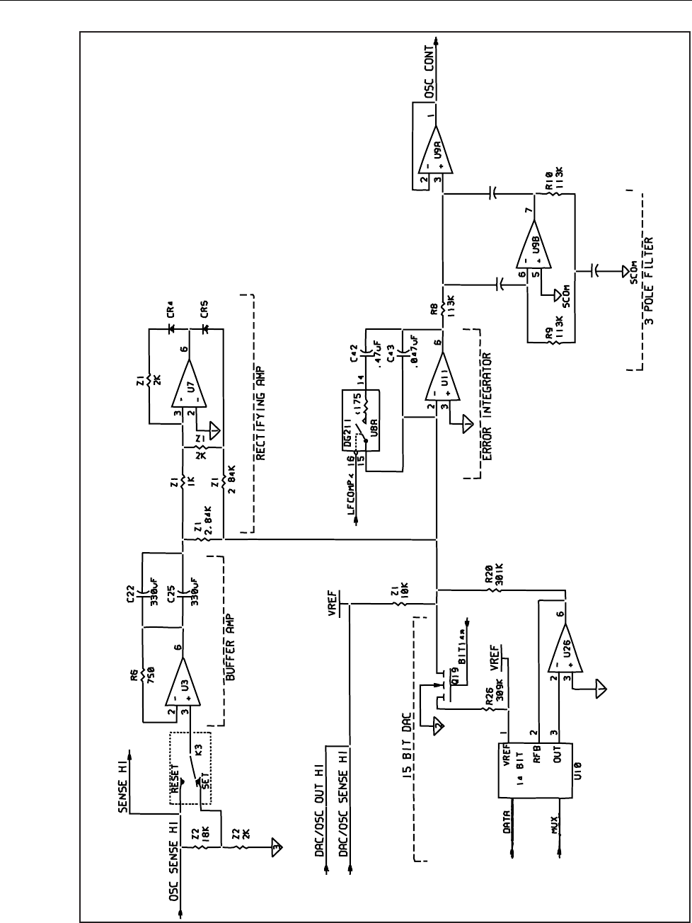
5700A/5720A Series II Calibrator
Service Manual
2-76
ahp017f.eps
Figure 2-19. Oscillator Control Analog Control Loop

Theory of Operation
Analog Section Detailed Circuit Description
2
2-77
2-127. AC/DC Thermal Transfer Circuit
Refer to Figure 2-20 for the following discussion. The ac/dc thermal transfer circuit
achieves basic mid-band amplitude accuracy. This is done by first applying the reference
voltage (VREF) to the thermal rms sensor (U14) and measuring the output. Next, the ac
voltage is applied to the thermal rms sensor and the dc output is compared to the
previous reading. The sensor detects the difference between the ac and dc input voltages
to within a few ppm.
If there is an ac/dc difference, the dc reference current applied to the error integrator of
the analog control loop is adjusted via the 15-bit dac until the ac/dc difference is zero.
The ac/dc thermal transfer circuit that performs this function is further described in
detail. It contains the dc sense buffer, ac sense buffer, ac/dc thermal sensor, and the
square-root amplifier and 15-bit dac as outlined on the schematic.
As previously mentioned, the input to the thermal rms sensor is either the dc reference
voltage (VREF) buffered by the dc sense buffer or the ac voltage (SENSE HI) buffered
by the ac sense buffer.
The dc sense buffer circuit uses op amp U30 as a buffer amplifier. Enhanced-mode FET
Q10 provides feedback for U30 while FETs Q8 and Q9 are off. During a dc transfer,
control line AC*/DC and comparator U21C turn on the FETs, applying the output of the
dc sense buffer to the input of thermal rms sensor U14.
The ac sense buffer circuit contains op amps U12A, U12B, U13; FETs Q6, Q7, Q11,
Q12; relay K4, and associated components. Relay K4 selects the input resistance to
amplifier U13, which has a nominal inverting gain of 0.316 in the 22V range and 3.16 in
the 2.2V range.
During operation in the 22V range, relay K4 is set, feeding the input, SENSE HI,
through the 20 kΩ resistor in Z3. When operating in the 2.2V range, the 2.22 kΩ and
20.0 kΩ resistors in Z3 are put in parallel by K4 in the reset position, reducing the input
resistance to 2 kΩ.
During an ac transfer, control line AC*/DC and comparator U21D turn on FET Q12 so
the output of amplifier U13 is applied to the input of thermal rms sensor U14. At this
time, FET Q11 is turned off and the feedback path for U13 is through the 6.32 kΩ
resistor in Z3.
During a dc transfer, Q12 is off and comparator U21B turns on FET Q11, providing the
feedback path for U13. Op amps U12A and U12B provide low offset and increase the
gain. Control line HFCOMP and comparator U22C turn on FETs Q6 and Q7 during
operation in the 1 MHz range.
The output of either the dc sense buffer or the ac sense buffer becomes the input of
thermal rms sensor U14. During operation from 0.22V to 0.7V in the 2.2V range, or
2.2V to 7V in the 22V range, relay K7 is set, directly connecting the input signal to the
sensor. The input to the thermal sensor is through R31 by K7 in the reset position during
operation from 0.7V to 2.2V in the 2.2V range, or 7V to 22V in the 22V range.
Comparator U21A provides protection for thermal rms sensor U14. If the junction
temperature of the sensor goes above 200ºC, the voltage at pin 3 increases, driving the
output of U21A negative. This turns off the FETs controlling the output of the dc sense
buffer. The ac sense buffer gain goes to zero by turning on FET Q11.
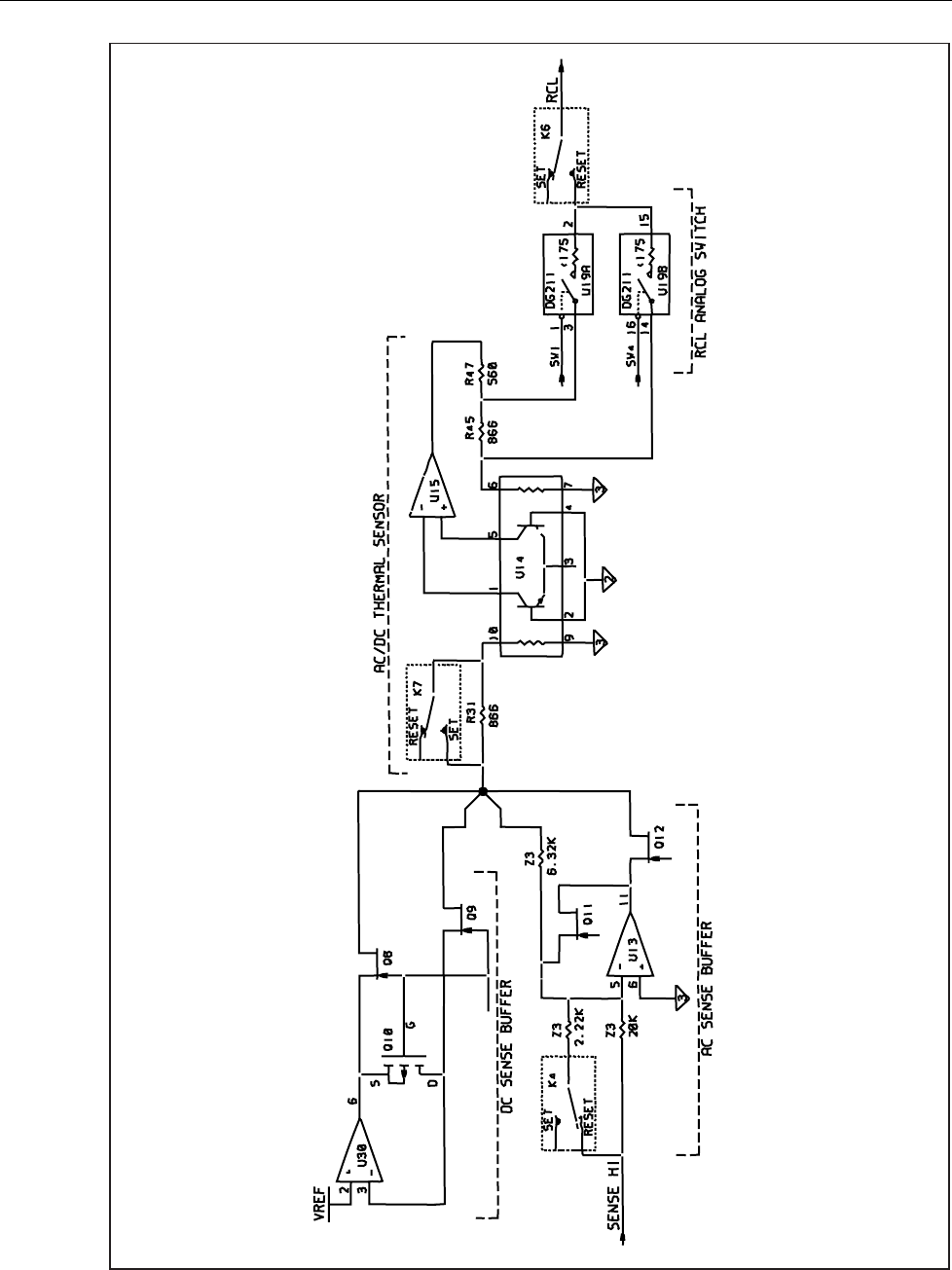
5700A/5720A Series II Calibrator
Service Manual
2-78
ahp018f.eps
Figure 2-20. AC/DC Thermal Transfer Circuit

Theory of Operation
Analog Section Detailed Circuit Description
2
2-79
The ac/dc thermal sensor and square-root amplifier, as outlined on the schematic, contain
the thermal sensor U14, op amp U15 and transistor array U17. The dc voltage from the
thermal sensor is connected to U15B configured as an integrator. Comparator U22B is
used to control FETs Q18 and Q20. These FETs are turned on, adding C84 and C62 to
the integrator, by control lines LFCOMP* and AC*/DC both at logic low. The output of
integrator U15B is used by the square-root amplifier contained in U15A, U15C and U17.
This circuit keeps the settling time of the sensor constant when its input is varied
between full and 1/3 scale. The output of the sensor is connected to the RCL line by
relay K6 and CMOS analog switch U19A and U19B. During operation from 0.22V to
0.7V in the 2.2V range, or 2.2V to 7V in the 22V range, sensor output is connected to the
RCL line through buffer U31, U19B, and K6 in the set position. During operation from
0.7V to 2.2V in the 2.2V range, or 7V to 22V in the 22V range, sensor output is
connected to the RCL line through U19A and K6. Control lines SW1 and SW4 control
U19A and U19B respectively. The RCL line is routed to the DAC assembly (A11) where
its amplitude is measured by the adc circuit.
To do an ac/dc transfer, the dc sense buffer is connected to the thermal sensor and the
sensor output is connected to the +input of the DAC’s adc circuit. The -input of the adc
circuit is connected to the DAC output (VREF), and the difference between the two is
measured and stored in memory. Next, the output of the ac sense buffer is connected to
the sensor and the sensor output is connected to the +input of the DAC’s adc circuit. The
difference is measured and compared to the previous reading. The difference between
these two readings is the difference in rms value of the ac and dc input voltages. If there
is an ac/dc difference, the dc reference current applied to the error integrator of the
analog control loop is adjusted via the 15-bit dac until the ac/dc difference is zero.
The 15-bit dac contains an AD7534 dac IC (U10), FET Q19 and op amp U26. The first
14 bits (bits 0-13) are generated by the dac IC U10, and bit 14 is generated by Q19, R26,
and control line BIT14. Control busses DATA and MUX from the digital control circuit
select the data and address for U10. The output is inverted by U26 to create 14 BIT DAC
OUT, which is applied to the summing node of the error integrator by R20. This output
is also monitored by the diagnostic circuit.
2-128. Oscillator Calibration
Calibration consists of determining the offset and gain errors of the ac/dc switching
circuitry. Errors are measured at dc using the calibrator DAC and the 6.5V reference as
the primary sources of accuracy. This characterization is valid for frequencies up to 1
kHz. Above 1 kHz, ac/ac characterization is used to ensure the output accuracy.
The DAC assembly (A11) is set to 0V with its output connected to the ac sense buffer
(via SENSE HI) by relay K1 in the set position. The output of the ac sense buffer is
connected to the RCL line by K6 in the set position and by control line GCAL and
comparator U22A turning on Q13. The 0V input is stored as Vin1. The output measured
by the adc circuit on the DAC assembly is stored as Vout1.
Relay K1 ties 6.5V reference BRF6 and BSRF6 to VREF, where it is measured at the
output of the thermal sensor in the same manner as a dc transfer. This measured output is
stored in memory.
The DAC output is set to 20V or 2V and is measured at the output of the thermal sensor
in the same manner as an ac transfer. The DAC is then adjusted until this measured
output is the same as stored in the previous step. The DAC setting is stored as Vin2 and
the 6.5V reference is Vout2. The gain can now be calculated with the formula: (Vout2 -
Vout1)/(Vin2 - Vin1).

5700A/5720A Series II Calibrator
Service Manual
2-80
2-129. AC/DC Frequency Response Characterization
Characterization is accomplished by first performing an ac/dc transfer with the Oscillator
Output set to a low frequency. The ac/ac thermal sensor circuit, containing the thermal
sensor U16 and op amp U15D, characterizes the frequency response of the main ac/dc
thermal sensor. This sensor has no active circuitry at its input, and all switching is done
by relays to ensure a flat frequency response.
In the 20V range, the Oscillator Output is switched through R34 to the ac/ac thermal
sensor via SENSE HI, K5, and K9 in the set position. In the 2.2V range, R34 is bypassed
by K9 in the reset position. The output of this sensor is routed to the RCL line via U19C
and K6. A reading is taken and stored in memory as ACref.
The output frequency of the Oscillator Output is changed to the first cal point and the 15-
bit dac is adjusted until the reading from this ac/ac thermal sensor is the same as ACref.
The RCL line is then switched back to the ac/dc thermal sensor. A reading is taken
stored in memory as ACdif. The gain constant is calculated using the formula (ACdif +
Vdac)/Vdac, where Vdac is the DAC assembly (A11) voltage.
This ac/ac transfer function is also performed for the 220V range and the 1100V range.
These ranges are generated by the Power Amplifier assembly (A16) and the High
Voltage/High Current assemblies (A14 and A15). High voltage ac signals are attenuated
and connected to AC CAL, where they are connected to the sensor though relay K5 in
the reset position. In the 220V range, the output of the sensor is divided by Z4 and
connected to the RCL line by U19D and K6.
Protection for this thermal sensor is provided by comparator U22D, FET Q14, zener
diodes VR5, VR6, resistor network Z10, and diodes CR12 and CR13. During normal
operation, U22D keeps Q14 off. If the junction temperature of the sensor goes above
200ºC, the voltage at pin 3 increases, driving the output of U22D positive. This turns on
Q14, shunting the input of the sensor to common through CR12 and CR13.
2-130. Oscillator Output Assembly (A13)
The Oscillator Output assembly is controlled by the Oscillator Control assembly. Refer
to Figure 2-21 and the schematic diagram for the following discussion.
The Oscillator Output assembly generates an ac sine wave from 0.22V to 22V with a
frequency range of 10 Hz to 1.1999 MHz. There are five frequency ranges (100 Hz, 1
kHz, 10 kHz, 100 kHz and 1 MHz) and two voltage ranges (2.2V and 22V). The output
signal is either routed to the OUTPUT binding posts, or it is used internally by the Power
Amplifier, High Voltage, Wideband AC Module (Option -03), Current, or Switch Matrix
assemblies, or it is routed to an Auxiliary Amplifier for generation of voltages and/or
functions outside this range. Output sensing is available for all voltage ranges above 220
mV at the SENSE binding posts.
The Oscillator Output assembly contains a fixed-amplitude quadrature RC oscillator, a
0.22-22V digital/linear gain-controlled amplifier, a fixed-amplitude variable phase-
shifting network, phase-locked loop control circuitry for phase locking to an external
signal or the PLOCK signal from the Current/Hi-Res assembly (A7), and digital control
circuitry.
All power supplies used by this assembly except the -12S supply are generated by the
Guard Crossing/Regulator assembly (A17). The -12S supply is generated on this
assembly by a three-terminal -12V regulator (U2) using the -17S supply as its input.
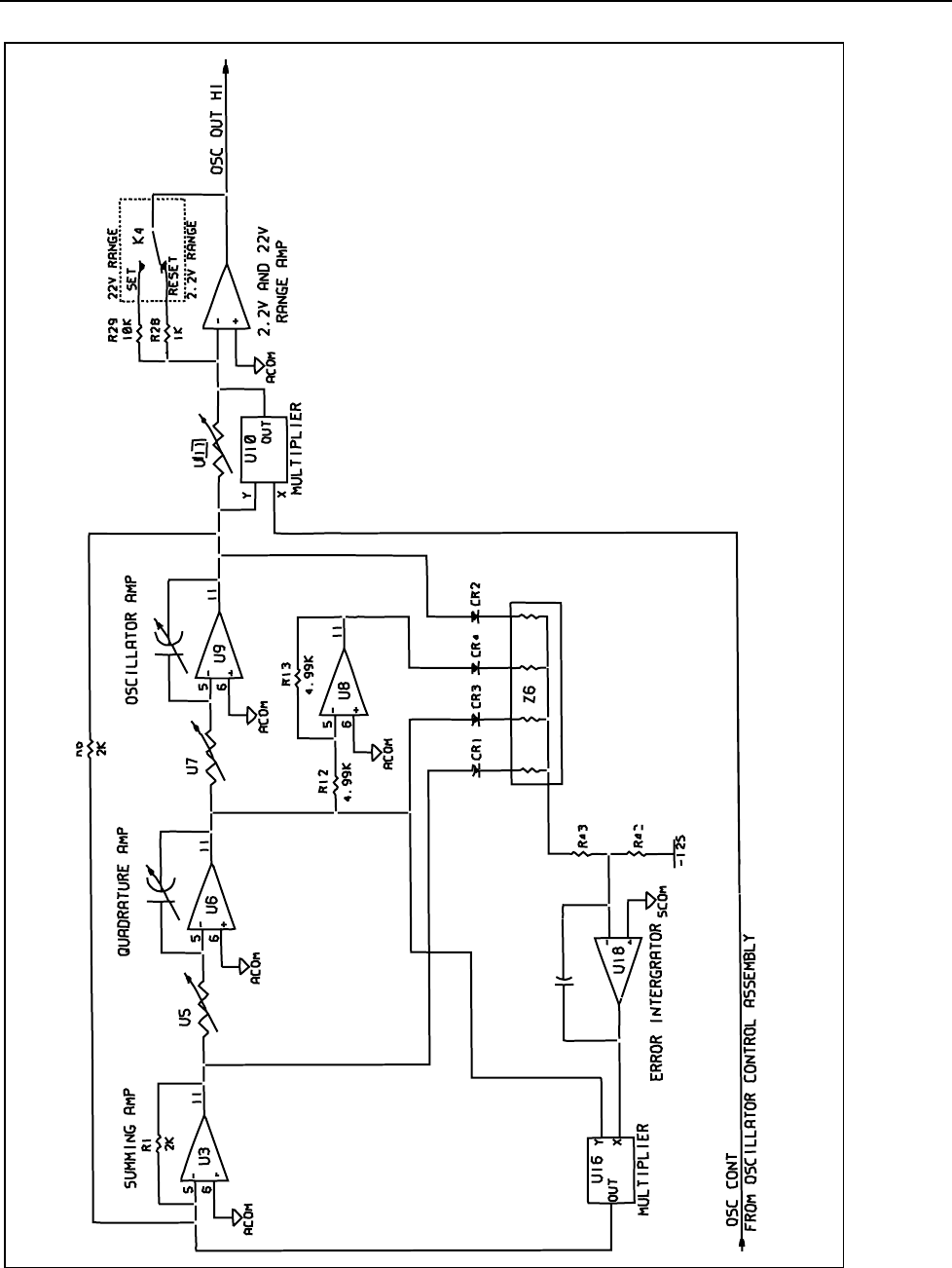
Theory of Operation
Analog Section Detailed Circuit Description
2
2-81
ahp019f.eps
Figure 2-21. Quadrature RC Oscillator Circuit

5700A/5720A Series II Calibrator
Service Manual
2-82
2-131. Oscillator Output Digital Control
The digital control circuit consists of an 82C55 Programmable Peripheral Interface
(U26), a 5801 Latching Relay Driver (U24), and three HC374 Octal D-Type Flip Flops
(U12, U32, U33). The Programmable Peripheral Interface (U26) is under software
control via the guarded digital bus and has three ports which generate 24 outputs. Port A
(PA0-PA7) is a common input bus for U24, U12, U32, U33, and U28. Latching relay
driver U24 controls the four latching relays K1-K4. Relays K1-K3 select the frequency
range and K4 selects the voltage range. This IC is strobed by PC3 of port C and enabled
by PC6 of port C. To ensure that the relays are latched properly the driver must be
enabled for 10 ms.
Latch U32 is clocked by PC0 and generates the data bus FREQ DATA for controlling 8-
bit resolution hybrid resistive dacs U5 and U7. Latch U12 is clocked by PC1 and
generates the data bus AMPL DATA for controlling U11, which is identical to U5 and
U7. Latch U33 is clocked by PC2 and generates control bus PHASE, which controls
multiplexer U27 in the phase shifter circuit and control bus MUX, which controls the
SDL multiplexer U25 in the diagnostic circuit. This diagnostic circuit monitors the ±44S
supplies, ±15S supplies, INTEGRATOR OUT, LOOP FILTER OUT, and AMP1 which
is from U30, the A13A1 assembly. These voltages are divided by Z2 and Z3 and
connected to the SDL line by multiplexer U25, where they are measured by the adc
circuit on the DAC assembly (A11).
PB0-PB2 of port B generates control bus PLOCK RNG which is used in the phase-
locked loop circuit. PB4 is control line 0/180 to control FET Q7 via comparator U31B in
the phase-locked loop circuit. PB6 is control line LFCOMP* to control FET Q6 via
comparator U20A in the integrator circuit. PB7 is control line HFCOMP*, which is
routed to the Oscillator Control assembly (A12). PC4 and PC5 are control lines DAC
STRB and DAC SEL respectively, which control the dual 8-bit dac U28 in the phase
shifter circuit. PC7 is control line INH to enable the multiplexer U25 in the diagnostic
circuit.
2-132. Quadrature RC Oscillator
The quadrature oscillator is a double integrator type. It contains two op amp RC
integrators and a unity-gain inverting summing amplifier. The integrators are identical
and use relay-switched feedback capacitors to select five frequency ranges. An 8-bit
resolution resistive dac selects frequency within a range.
The summing amplifier uses op amp U3 to provide a 180º phase shift in the oscillator
loop at unity gain. Its exact phase shift and gain are adjusted by the amplitude control
and phase-locked loop circuits to satisfy the conditions required for amplitude stable
oscillation: exactly 360º loop-phase and unity gain. This amplitude control circuit uses
an integrator and multiplier as outlined on sheet 1 of the schematic. These two circuits
are described in detail later.
The two op amp RC integrators are the quadrature amplifier and the oscillator amplifier.
Their purpose is to provide -90º each to the loop phase with an amplitude slope of -
20dB/decade. The quadrature amplifier contains op amp U6, 8-bit resolution resistive
dac U5, and relays K1B, K2B, and K3B. The relays select feedback capacitors C25, C24,
C22, and C21 for frequency ranges 100 Hz, 1 kHz, 10 kHz and 100 kHz respectively.
For the 1 MHz range, all the above capacitors are removed from the loop, and the only
feedback path is C19. The input resistor is the 8-bit resolution resistive dac U5 which is
under the control of the FREQ DATA bus from the digital control circuit. Its equivalent
resistance is R = (256/X)*2 kΩ, where X is the digital code on the FREQ DATA bus.
The oscillator amplifier contains op amp U9 and performs the same function as the
quadrature amplifier. Its input resistance is controlled by resistive dac U7. Relays K1A,
K2A, and K3A select the feedback capacitance. Since their phase shift is constant with

Theory of Operation
Analog Section Detailed Circuit Description
2
2-83
frequency and the sum of the phase shifts around the loop is zero for all frequencies, we
have satisfied one half of the requirement for oscillation. In summing the gain in dB
around the loop it is apparent that unity gain occurs at only one frequency. This happens
when the closed loop gains of the integrators are unity. This corresponds to F = 1/(2 x PI
x R x C), which is the frequency of oscillation.
2-133. Oscillator Amplitude Control
Since small excess phase shifts exist in all three amplifiers and the gain of the summing
amplifier cannot be made exactly one, it is impossible to generate an amplitude-stable
sinusoidal waveform from just these elements. A control circuit consisting of an error
integrator and a linear four-quadrant multiplier is used to sense the output amplitude and
stabilize it by adjusting the loop phase shift slightly.
To do this, a fourth oscillator signal is generated using U8 to invert the output of the
quadrature amplifier. The Oscillator now has four equal-amplitude signals all spaced 90º
apart. These signals are rectified and summed by CR1-CR4 and Z6 in such a way that a
dc representation of the output amplitude is created. This dc signal is summed with a -
12V reference voltage by the error integrator circuit which contains op amp U18. If there
is a magnitude difference between the rectified dc and the reference, the output of the
error integrator changes. This in turn controls the amplitude of the oscillation. This is
done via multiplier U16, a linear-variable resistance with a value inversely proportional
to the error integrator output voltage.
If the control input (x input) to the multiplier is zero, the equivalent resistance from the
signal input (y input) is infinite. If the control input is negative, the equivalent resistance
is negative. The Y signal input of the multiplier is the quadrature amplifier output. Any
nonzero control voltage changes the phase shift of the loop by injecting a small amount
of out-of-phase current into the summing amplifier. This negative feedback is used to
stabilize the amplitude of the oscillating signal by allowing one output amplitude only to
satisfy the required conditions of oscillation. During operation in the 100 Hz range,
control line LFCOMP* and comparator U20A turn off FET Q6.
2-134. Phase
−
locked Loop
The Oscillator Output assembly is phase locked to an external frequency to increase
frequency accuracy. This external frequency comes from the High-Resolution Oscillator
on the Current/Hi-Res assembly (A7) or from an external source connected to the rear-
panel PHASE LOCK IN jack.
The frequency capture range is approximately ±5% of the nominal output frequency
range. This is done by comparing the oscillator output frequency SUMMING AMP OUT
or INT OSC OUT against the external frequency source P LOCK HI with a phase
detector. The P LOCK HI signal is referenced to P LOCK LO. The phase-locked loop
circuit locks SUMMING AMP OUT to the external frequency when the calibrator is in
the 22V range or less. The phase-locked loop circuit locks INT OSC OUT, which is 180º
out of phase from SUMMING AMP OUT, during calibrator operation at higher voltages.
This occurs because the output from the Power Amplifier and High Voltage assemblies
(which are used to generate the higher voltage ranges) are 180º out of phase from the
Oscillator output. When the Calibrator is in the higher voltage ranges, control line 0/180
and op amp U31B turn on Q7, which selects INT OSC OUT to the Zero Crossing
Detector.
Since the phase detector circuit requires digital inputs, both signals are converted to
square waves using U23A/B as dual zero crossing detectors. Square waves from the zero
crossing detector circuitry are fed to the phase detector circuit containing U22A/B and
U21. The phase detector circuit looks for the falling edge of both signals. The first signal

5700A/5720A Series II Calibrator
Service Manual
2-84
that makes a positive to negative transition causes the phase detector to turn on either the
positive (CR5, CR6) or the negative (CR7, CR8) charge pump, depending on which
signal is first. The Charge Pump is turned off when the other signal makes its transition.
Thus the signal with the highest frequency has its respective charge pump pulsed on and
off while the other charge pump remains off.
The accumulated charge is integrated by the loop filter circuit, which contains op amp
U31A, multiplexer U17, Z1, and C75-C84. Multiplexer U17 is controlled by the PLOCK
RNG control bus from the digital control circuit. This multiplexer changes the cross-over
point of the loop filter by selecting C83 and C84 for feedback in the 100 Hz range.
Capacitors C81 and C82 are used for the 1 kHz range, C79 and C80 for the 10 kHz
range, C77 and C78 for the 100 kHz range, and C75 and C76 for the 1 MHz range.
The output of the loop filter controls two multipliers (U15 and U19) similarly to the
amplitude control section. The only difference is that the signal input is derived from the
in-phase signal. In the case of U15, the input signal is QUADRATURE AMP OUT,
which changes the unity-gain frequency of the oscillator amplifier. In the case of U19,
the input signal is SUMMING AMP OUT, which changes the unity-gain frequency of
the quadrature amplifier. The new frequency of oscillation is the new unity gain
frequency of the integrators. Under phase-locked conditions, neither charge pump is
allowed to turn on because neither signal reaches the phase detector first.
2-135. 2
.
2V and 22V Range Output Amplifier
The 2.2V and 22V range output amplifier is an inverting wide-band low-distortion
amplifier that provides output signal OSC OUT HI at the OUTPUT binding posts in the
2.2V and 22V ranges. OSC OUT HI is used by the Power Amplifier and High Voltage
assemblies to generate the higher voltage ranges.
This amplifier uses a surface-mount gain block (U30) called the Oscillator Wideband
SMD PCA (A13A1) and a complementary Darlington emitter follower bootstrapped
output stage. Relay K4 selects feedback resistor R28 for the 2.2V range and R29 for the
22V range. It also changes the open-loop frequency response for each voltage range. Its
gain within a range is controlled by the gain control multiplier circuit and the dac gain
control circuit.
The dac gain control circuit contains the same 8-bit resolution resistive dac (U11) as in
the oscillator with the exception that it is controlled by the AMPL DATA control bus
from the digital control circuit. This resistive DAC provides the coarse gain control. The
gain control multiplier circuit contains a multiplier U10, which provides a small linear
control range of several dac counts. The control input to the multiplier, OSC CONT,
comes from the Oscillator Control assembly (A12). This allows the output amplitude to
be adjusted as required by the Oscillator Control Assembly. The theory of operation for
the rest of the output stage is described following the A13A1 theory.
2-136. Oscillator Wideband Smd Assembly (A13A1)
The A13A1 is a surface-mount assembly on the Oscillator Output assembly (A13) that
provides the 22V output signals of the Calibrator. It is essentially an operational
amplifier built using discrete components to provide the necessary speed, power output
and breakdown voltage required for such a high output signal.
The input stage is a differential pair (Q2 and Q3) that is buffered by a source follower
Q1. The transconductance is determined by R3, R4 and R26. The inherent input offset
voltage of this stage is corrected by U1 and U2 and related components. The output of
Q3 is level-shifted by VR5-VR7 before being applied to the mid stage. Transistor Q4
serves as a high-impedance current sink used to bias the input stage to approximately 10
mA. Potentiometer R30 adjusts the dc zero at the output of U2.

Theory of Operation
Analog Section Detailed Circuit Description
2
2-85
The mid stage is a common-emitter, Miller-compensated gain stage (Q5) that drives a
common-base level shifter (Q13) on the Oscillator Output assembly. This stage is
current limit protected by R12 and Q4. The dominant pole is set with the Miller
capacitor C5 and the input stage transconductance. The mid stage is biased to 10 mA by
Q6 and related components.
The output stage of the amplifier is a bootstrapped complementary Darlington pair. The
only parts of the output stage on this A13A1 assembly are the input transistors Q7 and
Q8. The output bias current is set by R17 and CR4-CR5 to be approximately 40 mA.
This keeps the output stage class A for all normal output conditions.
2-137. Output Stage
The output stage circuit is a complementary Darlington emitter follower bootstrapped
buffer amplifier. The input transistors are Q7 and Q8 on the A13A1 assembly. These
transistors drive the output transistors Q8 and Q14 respectively. Transistors Q10 and
Q11 in the positive side and Q16 and Q17 in the negative side are parallel transistors
bootstrapped by VR3 and VR4. Current sources CR13, CR14, CR17, CR18, CR15,
CR16, CR11, and CR20 provide the bias current for their respective bootstrapped
transistors. Current limiting for the positive side is provided by Q9 and R91. During an
overcurrent condition, the voltage drop across R91 turns on Q9, which draws current
away from the base of Q11. Current limiting is done in the same manner for the negative
side with Q15 and R99.
Switch S1 can be switched to pull the input of the A13A1 output stage low for
troubleshooting the output stage. Refer to the Oscillator Output troubleshooting section
for more information.
2-138. Phase Shifter
The phase shifter circuit provides a fixed amplitude variable phase auxiliary signal at the
rear panel of the calibrator. This signal is the same frequency as the output, but can be
phase shifted over a 360º range. The four phases (each 90º apart) for the oscillator circuit
are divided by Z4 and Z5. These signals are connected to the dual four-channel
multiplexer (U27), which is under the control of the PHASE control bus from the digital
control circuit. This multiplexer selects any two adjacent oscillator phases (e.g. 0º and
90º) that are connected to the input of a dual monolithic DAC U28. These signals are
then scaled by the dac (U28), also under the control of the digital control circuit. The two
outputs of this dac are summed by op amp U29. Using this method, the output of U29 is
a phase shifted signal between 0 and 360º, where the scaling of the signals phase shift
within a 90º range.
2-139. Power Amplifier Assembly (A16)
The Power Amplifier assembly outputs dc voltages from ±22V to ± 219.99999V and ac
voltages from 22V to 219.99999V rms. The frequency limit for 220V ac output is 100
kHz. Output voltage limits are derated at frequencies above 100 kHz. At 1 MHz, the
maximum output voltage is 22V rms. The Power Amplifier drives the High Voltage
assemblies (A14, A15) in all high voltage and high current functions.
This assembly also contains calibration circuitry that enables the internal calibration
system to determine exact Power Amplifier ac and dc gain, offsets and frequency
response.
The main sections of this assembly are the input stage, mid stage, output stage, sense-
current cancellation circuit, the dc and ac gain calibration circuits, and the Power
Amplifier Digital Control SIP assembly (A16A1), which is mounted on the Power
Amplifier assembly.

5700A/5720A Series II Calibrator
Service Manual
2-86
2-140. Power Amplifier Digital Control Sip Assembly (A16A1)
Digital control for the Power Amplifier assembly is contained on the SIP assembly
(A16A1) mounted at the bottom of the Power Amplifier. This assembly configures the
Power Amplifier assembly for its various modes of operation. (Also see "±PA Supplies
Digital Control" in the Power Amplifier Supply theory of operation.)
The heart of the Digital Control assembly is an 82C55 Programmable Peripheral
Interface IC (U11) operating under software control via the guarded digital bus. This IC
has three ports that generate 24 outputs. These outputs control two 5801 relay driver ICs
(U10, U12), two LM339 Comparators (U13, U15) and an analog multiplexer (U14) used
for diagnostics.
Relay driver U10 generates eight control lines (LC0*-LC7*) that control four latching
relays (K1-K4). Relay driver U12 generates eight control lines (C0*-C7*) for non-
latching relays K10-K17. C0* also controls FETs Q57 and Q58. Port A (PA0-PA7) from
U11 provides an input bus common to relay drivers U10 and U12. Each driver has
separate strobe and enable lines from port C of U11. Driver U10 is strobed by PC7 and
enabled by PC5. Driver U12 is strobed by PC4 and enabled by PC6. When a STROBE
line is selected, data on the bus (PA0-PA7) is strobed into the respective driver chip.
When an ENABLE is selected, this strobed data appears at the output, thereby energizing
the appropriate relays. Latching relays only need to be energized for 10 ms; non-latching
relays need to be energized continuously.
As an example, the following steps are taken to set up latching relays controlled by relay
driver U10.
1. Write the proper data for these relays to port A of the 82C55 (U11).
2. Write hex A to PC4-PC7 to strobe the data into U10.
3. Write hex 0 to PC4-PC7, wait 10 ms and write hex 2 to PC4-PC7. This takes U10's
output out of tri-state and energizes the proper relay coils for 10 ms. Since PC4 and
PC6 are always low, U12 is undisturbed.
Two LM339 quad comparators (U13 and U15) get their data from port B of U11 (PB0-
PB7) and generate control lines SW0-SW7. SW0-SW2 are inputs to decoder U9, which
generates eight additional control lines (CONT0*-CONT7*) for controlling FETs and
solid state switches. Control line SW3 controls FETs Q50 and Q51. Control lines SW4-
SW7 are routed through the motherboard to the Filter/Power Amplifier Supply assembly
(A18) to control the +PA and -PA supplies.
The diagnostic circuit enables the Calibrator to monitor eight diagnostic (MUX) signals
on the Power Amplifier assembly. A 4051 analog multiplexer (U14) is controlled by
PC0-PC3 from U11. This multiplexer selects of the eight MUX signals to the SDL line,
where it is measured by the adc circuit on the DAC assembly (A11). Resistor network Z2
and various resistors and zener diodes on the Power Amplifier assembly divide these
MUX signals down to a proper level for measurement by the adc circuit. The eight
monitored points are:
• MUX0 Output of U7; indicates the status of the amplifier loop
• MUX1 +PA Supply
• MUX2 -PA Supply
• MUX3 Power Amplifier output
• MUX4 Indicates the temperature of the Power Amplifier assembly
• MUX5 Power Amplifier dc input
• MUX7 Diagnoses the state of the hybrid heater-control circuit
Theory of Operation
Analog Section Detailed Circuit Description
2
2-87
2-141. PA Common Circuitry
Common circuitry consists of the +PA and -PA supplies, input stage, mid stage, and the
output stage. These four circuits are described under the next four headings.
Power Amplifier input node, gain, and feedback are different for dc and ac operation.
Power Amplifier gain is -20 in the dc function, determined by the ratio of resistor
network bonded to the HR8 assembly (500 kΩ/25 kΩ). Gain in the ac function is -10,
which is determined by the ratio resistors [(R11 + R12 + R13)/R17]. This is described in
more detail under "DC Voltage Function" and "AC Voltage Function".
2-142. +PA and -PA Supplies
The ±PA supplies are high voltage supplies generated by the Filter/PA Supply assembly
(A18). These supplies can be controlled by the Digital Control SIP assembly (A16A1)
and are switched between the two modes shown in Table 2-13.
• ±185V
• ±365V
Theory of operation for the Filter/PA Supply assembly (A18) describes how these
voltages are generated and selected.
Table 2-13. PA and -PA Supply Settings at Different Outputs
Calibrator Output +PA -PA
Less than 22V ac or dc +185V -185V
22 to 110V dc +185V -185V
110 to 220V dc +365V -185V
-220 to -110V dc +185V -365V
22 to 101V ac (freq < 120 kHz) +185V -185V
22 to 85V ac (freq > 120 kHz) +185V -185V
Other voltages +365V -365V
220 to 550V dc or ac +185V -185V
550 to 1100V dc or ac +365V -365V
220 mA to 2.2A +365V -365V
2-143. PA Input Stage
The input stage consists of a heater-controlled hybrid HR8, op amp U7, transistor Q6,
and JFET Q2. The HR8 assembly consists of an op amp mounted on a heated-substrate
hybrid, with a resistor network bonded to it. Hybrid HR8 provides the input stage with
excellent dc characteristics of low offset, noise and drift. The hybrid heater-control
circuit (on sheet 3 of the schematic) adjusts the base voltage of Q38 to deliver the correct
current to the heater resistor. This maintains the hybrid assembly at a constant
temperature in spite of environmental temperature variations. Transistor Q35 protects the
hybrid in case Q38 fails. Input of the hybrid op amp is protected by CR13 and CR14.
Output of the hybrid op amp is connected to the input of a faster op amp (U7), which
provides additional dc gain and a higher slew rate. JFET Q2 and transistor Q6 combined
with these two op amps complete the input stage. Q2 is a very low-bias-current, high-
frequency JFET.
In mid to high-frequency operation, Q2 is effectively the only path for the input stage
signal. HR8 and the U7 op amps are bypassed at these frequencies by R89, C42, R24,
and C12. As a result, the base of Q6 is at ac ground. In dc to mid-frequency operation,

5700A/5720A Series II Calibrator
Service Manual
2-88
the gate of Q2 is at ground potential. At any frequency, the potential difference between
the gate of Q2 and the base of Q6 results in a current through Q6 as determined by R22,
and by the transconductance of Q2 and Q6. The input stage is called a transconductance
stage because an input voltage results in a current output at the collector of Q6.
This current output is coupled to the mid stage (Q12, Q14, and Q16) by Q8, Q9, Q13 and
C15, where it results in a voltage across the base-emitter of Q16 (the input of the mid
stage). Current source Q9 determines bias current in Q2 and Q6. Variations of Q6 output
current become voltage variations at the base of Q16. This transfer is through Q8 and
Q13 at dc and low frequencies, and through C15 at high frequencies.
The input stage operates with low voltage supplies (±17V) whereas Q16 of the mid stage
is connected to the -PA supply, which can be as high as -365V. This potential difference
is dropped across level shifter Q13.
2-144. PA Mid Stage
The mid stage (Q12, Q14, and Q16), biased by the 8 mA current source (CR53, Q31,
Q32 and R87 on sheet 2 of the schematic), is a voltage amplifier providing additional
gain. The base of transistor Q16 is the input to the mid stage. MOSFETs Q12 and Q14
are biased by R41 and R53 respectively. Components CR21, CR23, and VR22 protect
Q12 from excessive source-to-gate voltage, and R112 prevents Q12 from oscillating.
Components CR25, CR29, VR28, and R113 perform the same function for Q14. A signal
at the base of Q16 appears amplified at the drain of Q12. Total impedance from the drain
of Q12 to ground, divided by R58, determines gain at dc and low frequencies. At high
frequencies, the effective drain to ground impedance is R53. Relay K12A parallels C18
and C57 during dc operation for a lower bandwidth. Capacitors C18 and C57 provide the
Miller capacitance for the amplifier.
Transconductance gain of the input stage and the Miller capacitance determine Power
Amplifier frequency response at high frequencies. All the voltage gain of the Power
Amplifier comes from the input and mid stages.
2-145. PA Output Stage
The Output Stage is an emitter follower that provides current gain but no voltage gain. It
is needed because the mid stage cannot drive the rated load by itself.
Voltage across R74 and R35 determines the bias current through the output stage. This
voltage equals the voltage across Q7, minus the value (4 x Vbe) (for each transistor Q4,
Q5, Q10, and Q11). Transistor Q7 is configured as a Vbe multiplier, the voltage across
which (and thus the output stage bias current) is the value (1 + (R23+R26)/R32). The
output bias current is 50 mA.
NMOSFETs Q1, Q3, and transistor Q5 source current, while PMOSFETs Q15, Q17, and
transistor Q10 sink current from the load. This output stage can drive up to 50 mA of
load current as determined by the current limit circuit on ±PA supplies on the Filter/PA
Supply assembly (A18).
Zener diodes VR15 and VR18 bootstrap MOSFETs Q3 and Q15 respectively, and
provide the power supplies SC+ and SC- to op amp U1 in the sense current cancellation
circuit. Two stacked NMOSFETs (Q1, Q3) on the top end (+PA side), and two stacked
PMOSFETs (Q15, Q17) on the bottom end (-PA side) withstand the high voltage drops
between ±PA supplies and output. NMOSFETs Q1 and Q3 are biased by R15 and R19
respectively. PMOSFETs Q15 and Q17 are biased by R52 and R57 respectively.
Components CR5, CR7 and VR6 protect Q1 from excessive source-to-gate voltage and
R108 prevents Q1 from oscillating. Protection is also provided for remaining MOSFETs
in the output stage. Output of this stage, called PA OUT HI, is the output of the Power
Amplifier assembly. Components R120 and L10 isolate capacitive loads.

Theory of Operation
Analog Section Detailed Circuit Description
2
2-89
2-146. PA Sense Current Cancellation Circuitry
During dc operation of the Power Amplifier, sense current in the 500 kΩ feedback
resistor (on the resistor network in the HR8 assembly) can cause an output error because
of the finite resistance path of the connection to the load. Op amp U1 eliminates this
error by feeding an equal and opposite current in this path. The magnitude of this current
is determined by PA OUT HI, which is connected to the non-inverting input of U1. This
circuit generates a current through R8, which is equal to current flowing through the 500
kΩ feedback resistor. Sense-current cancellation is active only in dc 220V range.
2-147. PA in Standby
The Power Amplifier schematic shows all relays and DG211 FET switches in the
standby condition. The Power Amplifier 25 kΩ input resistor and R17 are tied to OS
COM through Q39 and R118. Power Amplifier output is close to zero and the whole
loop is stabilized.
To better understand Power Amplifier configuration in the ac/dc 220V range, refer to
Figure 2-22.
2-148. PA Operation: 220V DC Range
During dc operation, Power Amplifier gain is -20, as determined by the 500 kΩ/25 kΩ
resistor network on the HR8 assembly. Control line SW3, inverted by U8, turns on Q51.
This references the +input of the precision op amp in the input stage to R COM. The
DAC assembly is set to the negative 11V range and its outputs, DAC OUT HI and DAC
SENSE HI, are connected to pin 2 of the resistor network on the HR8 assembly by relay
K2. The sense current cancellation circuit is active during dc operation. Its output, SIG1,
is connected to the resistor network feedback resistor pin 1 by relay K15A. The amplifier
has a much lower bandwidth in this mode because of the much higher Miller capacitance
in C57. Lower bandwidth results in lower amplifier noise.
The output signal, PA OUT HI, is routed to the High Voltage Control assembly (A14),
where it goes through relay K10 and becomes PA OUT DC. PA OUT DC is routed to the
Switch Matrix for connection to the OUTPUT HI binding post. The sense signal, PA
SENSE DC from the Sense Current Cancellation circuit, is routed to the Switch Matrix
assembly (A8) for connection to the OUT/SENSE HI or SENSE HI binding posts, thus
making the binding post the sense point in internal sense and allowing for external sense
through the SENSE HI binding post.
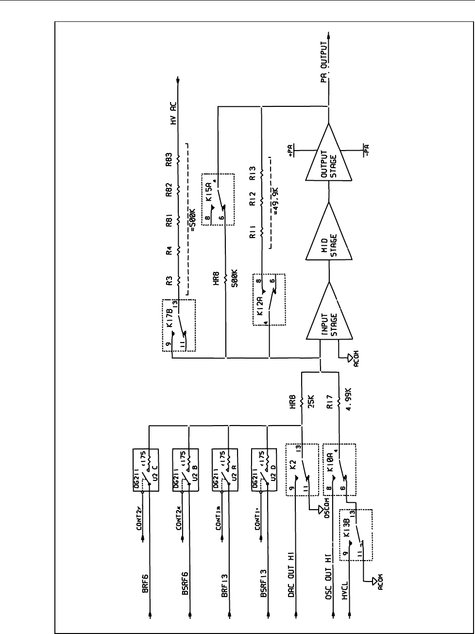
5700A/5720A Series II Calibrator
Service Manual
2-90
ahp020f.eps
Figure 2-22. Power Amplifier Simplified Schematic

Theory of Operation
Analog Section Detailed Circuit Description
2
2-91
2-149. PA Operation: 220V AC Range
During ac operation, Power Amplifier gain is -10 as determined by the 4.99 kΩ input
resistor R17, and 49.9 kΩ feedback resistors (R11 + R12 + R13). Control line SW3 turns
Q50 on, which references the +input of the precision op amp in the input stage to OS
COM. The Oscillator assembly (A13) is set to the 22V range and its output OSC OUT
HI is connected to the input resistor R17 by relay K10A. The Power Amplifier output is
connected to the feedback resistors R11-R13 by relay K12B.
The Power Amplifier output is attenuated by a precise 1/100 by 220V range ac
attenuator. The attenuated signal is connected to OSC SENSE HI, where it is sent to the
Oscillator Control assembly (A12). The Oscillator Control assembly regulates the
Oscillator Output so that an exact calibrated ac signal appears at OSC SENSE HI. Since
the 220V range ac attenuator is completely characterized (as explained below), the exact
desired signal appears at PA SENSE AC and hence at the appropriate sense point at the
output.
The 220V range ac attenuator circuit contains op amp U4, a 400 kΩ/4 kΩ resistor
network Z1, and transistor Q54. PA SENSE AC, which is connected to PA OUT HI at
the load, is connected to the 400 kΩ input resistor (pin 1) of Z1 by relay K16. The 400
kΩ/4 kΩ node (pin 3) of Z1 is connected to the inverting input of U4.
During ac operation, control line C0* is inverted by U8, which turns on Q58 to connect
the non-inverting input to OSC RCOM. Transistor Q54 supplies current gain for the
output of U4 to drive the capacitance of the OSC SENSE HI line. This voltage is
connected to the 4 kΩ feedback resistor (pin 4) of Z1. The output is connected to OSC
SENSE HI by relays K10B and K11. The dc feedback 500 kΩ/25 kΩ resistor network
and the sense-current cancellation circuitry are disconnected by energizing K15.
The sense signal, PA SENSE AC, and the output signal, PA OUT HI, are routed to the
High Voltage Control assembly (A14), where relays K10, K13, and K3 connect them to
HV SENSE and HV OUT. HV SENSE and HV OUT are connected to the binding posts
by the motherboard relays in the same manner as in the 1100V high voltage mode. Refer
to the High Voltage assembly theory of operation for more information.
2-150. High Voltage Assembly Support Mode
2-151. High Voltage AC 1100V Range
During high voltage ac operation, the output of the Power Amplifier is routed to the
input of a step up/down transformer on the High Voltage Control assembly (A14).
Overall gain from the Oscillator Output to the High Voltage Output is -100 as
determined by the 4.99 kΩ input resistor R17, and 500 kΩ feedback resistor (R3 + R4 +
R81 + R82 + R83). Relay K10A connects the ac signal OSC OUT HI from the Oscillator
Output assembly to input resistor R17. Relay K12 remains open as shown on the
schematic, while K15 is energized to remove feedback used in 220V-dc operation.
Output from the High Voltage Control assembly, called HVAC on the schematic, is
connected to the feedback resistors. Relay K17B is energized to close the feedback loop.
Control line SW3 is high, which turns Q50 on and turns Q51 off. Because sensing back
to the Oscillator Control assembly is done by the High Voltage/High Current assembly,
the output of the 220V range ac attenuator is disabled from OSC SENSE HI by relay
K11.
2-152. High Voltage DC 1100V Range and Current 2.2A Range
Operation of the Power Amplifier is the same for the 1100V dc and the 2.2A current
functions. In these functions, the output of the Power Amplifier is routed to a step
up/down transformer on the High Voltage Control assembly (A14). The Power Amplifier

5700A/5720A Series II Calibrator
Service Manual
2-92
is configured the same as for 220V ac operation, except that the input is the square-wave
signal HVCL from the High Voltage Control assembly, rather than OSC OUT HI,
through relays K13B and K10A.
2-153. 220V DC Internal Calibration Network
The 220V dc internal calibration network determines the exact gains and offsets of the
power amplifier. This circuit uses part of the resistor network HR8 as the input
attenuator, and uses op amp U9, and zener diodes VR57 and VR58. Relay K4 connects
the output of this circuit to the RCL line.
Zener diodes VR57 and VR58 reduce the power supplies for chopper-stabilized
amplifier U9, which is used as a voltage follower.
2-154. PA Calibration
The following paragraphs describe how the Power Amplifier assembly is calibrated
during the internal portion of calibration, or calibration check. This process calibrate the
offset, gain, and frequency characteristics of the Power Amplifier.
The instrument measures the offset of the main amplifier (220V range). The DAC output
is amplified by the Power Amplifier, which is configured for the dc 220V range, and its
output connected to the internal cal zero amplifier located on the Switch Matrix
assembly. Output of this internal cal zero amplifier is channeled to the DAC’s adc
amplifier circuit by the RCL line. Input of the internal cal zero amplifier is first
connected to R COM where a checkpoint reading is taken by the DAC’s adc circuit. The
output of the Power Amplifier is then connected to the input of the internal cal zero
amplifier and the DAC output is adjusted to the checkpoint reading out of the zero
amplifier. This adjusted DAC output is a measure of the offset of the Power Amplifier.
Also, refer to the Switch Matrix theory of operation.
The 175 kΩ/25 kΩ (internal cal) resistor network located on HR8 is calibrated next (see
Figure 2-23). First the offset of the 220V dc internal cal amplifier is measured. This is
done by connecting pin 6 of 175 kΩ/25 kΩ resistor network to RCOM by relay K1, and
pin 7 to ACOM by U5C and relay K3. ACOM is connected to RCOM through 051
during this step. Output of this internal cal amplifier is connected to the RCL line by
relay K4, where it is measured by the adc circuit on the DAC assembly. As before, the
DAC’s output needed to obtain the checkpoint for this step represents the offset of the
internal calibration amplifier.
Resistor network attenuation is calibrated next. Components U5A, U5D and K3 connect
BSRF13 and BRF13 to the 175 kΩ end, while K1 connects R COM to the 25 kΩ end of
the resistor network. The resulting 1.625V at the output is connected to the RCL line by
relay K4, where it is connected to the +input of the adc amplifier circuit on the DAC
assembly. The DAC output is connected to the adc circuit -input, and adjusted until the
checkpoint reading is obtained. The exact value of this voltage is now known, so the
system software computes the exact attenuator ratio from this known voltage, BSRF13
value, and the previous offset measurement.
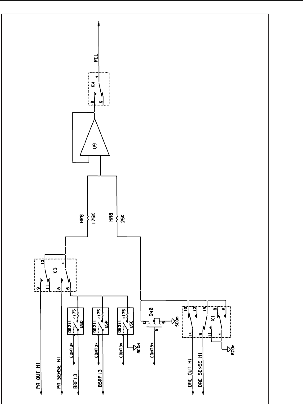
Theory of Operation
Analog Section Detailed Circuit Description
2
2-93
ahp021f.eps
Figure 2-23. Power Amplifier DC Calibration Network

5700A/5720A Series II Calibrator
Service Manual
2-94
Power Amplifier dc gain of approximately -20 is calibrated next. The Power Amplifier is
configured as in the 220V dc operation, except the input is connected to the DAC’s 6.5V
reference BRF6 and BSRF6 by U2C and U2D respectively. The resulting -130V at the
Power Amplifier output is connected to the 175 kΩ end of the internal cal resistor
network by relay K3. The 25 kΩ end of this network is connected to DAC OUT HI and
DAC SENSE HI by relay K1. The output of the internal cal amplifier is connected to the
DAC’s adc circuit as in the previous steps, and the DAC OUTPUT is adjusted until
checkpoint is measured by the adc circuit. Since the exact attenuation of the resistor
networks is already known, the exact Power Amplifier output voltage can be calculated.
This in turn gives the exact Power Amplifier dc gain, since the exact value of 6.5V
reference BSRF6 is known.
Attenuation of the 220V range ac attenuator (U4 and 396 kΩ/4 kΩ resistor network Z1)
is calibrated next. This is illustrated in Figure 2-24. First, the offset of the attenuator
circuit is measured by connecting the non-inverting input of U4 to ACOM through Q57
and thus to RCOM through Q51. Then, the Power Amplifier is configured for the 220V
dc range with its inputs connected to the DAC’s 6.5V reference BRF6 and BSRF6 by
U2B and U2C respectively. The resulting -130V is connected to the 400 kΩ input
resistor (Z1) of the 220V range ac attenuator by relay K16.
The +1.3V from the output of the attenuator circuit is connected to the RCL line by
relays K10B and K11. This voltage on the RCL line is connected to the +input of the adc
amplifier circuit on the DAC assembly. The DAC output is connected to the -input of the
adc amplifier circuit, and is adjusted until a null is achieved. The exact value of this
voltage is now known so the system software can compute the exact attenuator ratio.
The 220V range ac attenuator’s attenuation ratio can vary over the frequency range. This
variation can be accounted for if the frequency response of this network is characterized
at a few spot frequencies. This is done by connecting the Power Amplifier output, which
is set to 22V, to the AC CAL line by relay K14. The AC CAL line goes into the AC/AC
CAL thermal sensor located on the Oscillator Control assembly. The Power Amplifier
output of 22V is also attenuated through the AC Attenuator and sensed by the Oscillator
Control via OSC SENSE HI. The Oscillator adjusts its output, and hence the Power
Amplifier output, until the ac/ac cal thermal sensor measures the same ac level for all
these spot frequencies. The signal levels at OSC SENSE HI are stored in software at all
such points.
The ac/ac cal thermal sensor located on the Oscillator Control assembly has a flat
frequency response. The change in the ac attenuator’s output at various frequencies for a
constant thermal sensor output defines the frequency response of the Power Amplifier ac
attenuator. These computed ac attenuator factors are stored in the system memory and
are taken into account when the calibrator is configured to output ac voltages from the
Power Amplifier.
Output stage current is limited to about 250 mA; Q60 limits the current soured by the
output stage, and Q61 limits the current the output stage has to sink. Transistor Q62
limits the current flowing through the middle stage. These current limits both protect the
power amplifier circuitry and improve power amplifier transient response. Diode CR64
is a current source that maintains a current flow of at least 5 mA through the output
devices at all times.
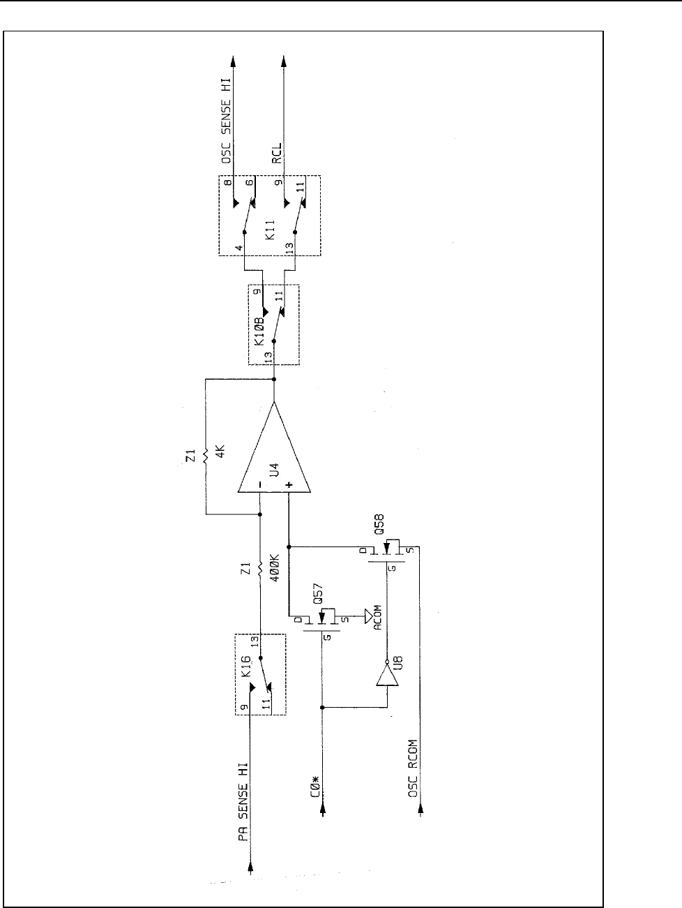
Theory of Operation
Analog Section Detailed Circuit Description
2
2-95
f2-24.eps
Figure 2-24. Power Amplifier Calibration AC Attenuator

5700A/5720A Series II Calibrator
Service Manual
2-96
2-155. High Voltage Assemblies (A14 and A15)
The High Voltage/High Current assembly (A15) and the High Voltage Control assembly
(A14) are used in with conjunction with other assemblies in the calibrator to generate the
±1100V dc, 1100V ac, and the 2.2A ranges. The two assemblies work together in
generating these ranges. This theory of operation explains how these ranges are
generated and discusses the individual circuits on each assembly. Refer to the High
Voltage/High Current assembly simplified schematics (Figures 2-24 through 2-28) or the
schematic diagram to understand this theory of operation better.
2-156. 1100V AC Range
Refer to Figure 2-25 for the following discussion. The ac signal generated by the
Oscillator Output assembly (A13) is amplified by the Power Amplifier assembly (A16).
The output of the Power Amplifier, PA OUT DC, is routed to the High Voltage Control
assembly (A14), where it is further amplified by transformer T1 to generate the 1100V
ac range. This high voltage signal from T1 is also the feedback signal to the Power
Amplifier assembly. Relays K14-K16 connect the transformer windings in series during
operation below 120 Hz.
Line PA OUT DC is connected to one side of the primary winding of step-up
transformer T1 by relay K1 on the High Voltage Control assembly (A14). The other side
of the primary winding is tied to PA COM through R67. One side of the secondary
winding is tied to PA COM by relays K9 and K6. The other side of the secondary
winding, the high voltage ac signal, is connected to HV OUT by relays K5, K12 and K3.
Line HV OUT is connected to the OUTPUT HI binding post by relays K9 and K1 on the
motherboard.
This high voltage ac signal is also connected to HVAC by relay K5. Line HVAC is the
feedback signal to the Power Amplifier assembly. During high voltage operation, the
input resistance of the Power Amplifier assembly is 5 kΩ. Line HVAC is connected to
the feedback resistance, which is a series of resistors totaling 500 kΩ. This creates a gain
of 100 to the Oscillator Output.
The SENSE HI binding post is connected to HV SENSE by relays K3, K2, and K10 on
the motherboard. HV SENSE, which is tied to HV OUT at the load, is connected to INT
HV SNS by relay K13 on the High Voltage Control assembly (A14). INT HV SNS is
routed to the High Voltage/High Current assembly (A15), where it is connected to the ac
sense buffer circuit by relay K6. This circuit attenuates the high voltage signal by 100
and connects it to OSC SENSE HI through relay K4B. The level of attenuation is
determined by the 7 MΩ input and 70 kΩ feedback resistors on the HR7 assembly. OSC
SENSE HI is used by the Oscillator Output assembly, which adjusts its output signal to
maintain an exact feedback signal level. HV OUT and HV SENSE are routed to the High
Voltage assembly (A15) where components CR9, CR10, and R33-R35 keep the voltage
difference between them at 0.7V should they become disconnected at the load. Relay
K11 connects HV OUT to HV SENSE during calibration in the ac function.
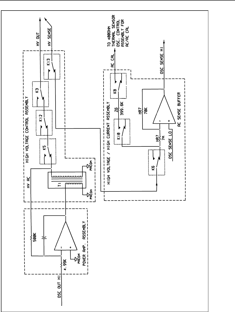
Theory of Operation
Analog Section Detailed Circuit Description
2
2-97
ahp022f.eps
Figure 2-25. High Voltage/High Current Assembly 1100V AC Range

5700A/5720A Series II Calibrator
Service Manual
2-98
2-157. 1100V DC Range
Refer to Figure 2-26 for the following discussion. The High Voltage assembly (A15)
amplifies the output of the DAC assembly (A11), set to the 11V range, by a gain of -100
to generate the 1100V dc range.
For operation in the 1100V dc range, DAC OUT HI and DAC SENSE HI from the DAC
assembly, set to the 11V range, are tied together and connected to the input of the dc HV
amplifier circuit by relay K1. The dc HV amplifier circuit, the HV dc output series pass
and current limit circuit, and the HV dc power supply circuit on the High Voltage
Control assembly (A14) constitute an overall amplifier with an inverting gain of 100.
This gain is determined by the 70 kΩ input and 7 MΩ feedback resistors on the HR7
assembly.
High voltage dc output, generated on the High Voltage Control assembly (A14), is
obtained by filtering an approximate trapezoidal wave. The overall loop gain of this
amplifier divides this ripple so the high voltage dc output is clean and stable.
Signal routing to the front panel binding posts is done in the same manner as the ac
1100V range.
2-158. HVDC Power Supply Filter Circuit
The high voltage dc power supplies are generated by the High Voltage Control assembly
(A14) in conjunction with the Power Amplifier assembly (A16). The High Voltage
Control assembly generates an amplitude-controlled square wave, HVCL, from the
magnitude control circuitry. The magnitude control circuit contains all the circuitry on
sheet 2 of the High Voltage Control assembly schematic.
Signal HVCL is amplified by the Power Amplifier assembly with its output, PA OUT
DC, connected to one side of the primary winding of transformer T1 by relay K1. The
other side of the primary is connected to PA COM by R67. The secondary windings of
T1 are connected to bridge rectifier CR1-CR4 by relays K9 and K6. The dc voltage from
this rectifier is called +HVDC and -HVDC. Resistors R3-R5 form a 600 kΩ bleeder
resistor for C1. Line HVDC is selected between +HVDC and -HVDC by relays K4 and
K11. Line HVDC is connected to HV OUT by relays K5, K12 and K3.
During operation with a negative DAC voltage and a positive output from the High
Voltage/High Current assembly, +HVDC is connected to HV OUT by relays K4, K11,
K5, K12 and K3. +SP C is created from -HVDC by relays K4 and K8. During operation
with a positive DAC voltage and a negative output from the High Voltage/High Current
assembly, -HVDC is connected to HV OUT by relays K4, K11, K5, K12 and K3. -SP C
is created from +HVDC by relays K4 and K8. Zener diodes VR4 and VR5 keep -SP C
and +SP C, respectively, from exceeding 16V. The dc voltage level of +SP C and -SP C
is controlled by the HV dc output series pass and current limit circuit on the High
Voltage/High Current assembly. This in turn controls the magnitude of HVCL which
sets the level of HVDC.
2-159. HV DC Output Series Pass and Current Limit Circuit
The HV dc output series pass circuit controls the level of +SP C when the high voltage
output is positive, and -SP C when the high voltage output is negative. Typically +SP C
and -SP C are approximately ±6.8V dc with ripple equal and opposite polarity from the
HVDC ripple.
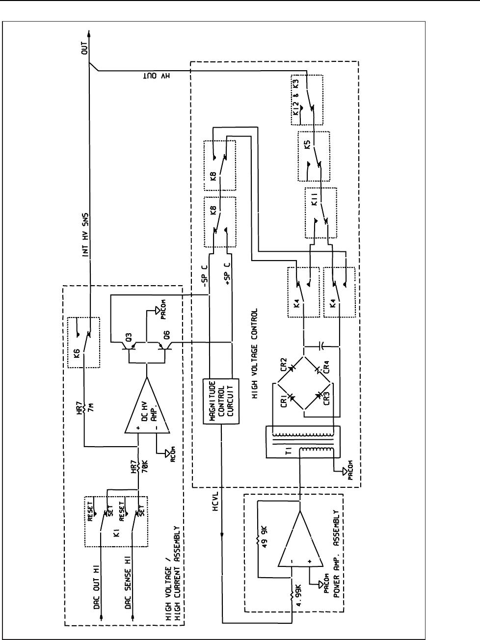
Theory of Operation
Analog Section Detailed Circuit Description
2
2-99
ahp023f.eps
Figure 2-26. High Voltage/High Current Assembly 1100V DC Range

5700A/5720A Series II Calibrator
Service Manual
2-100
When the DAC assembly is set to the +11V range, the output from the High Voltage
assembly (with a gain of -100) is in the -1100V range. In this mode, -SP C is connected
to the collector of transistor Q3. The output from the dc HV amplifier follows a change
in the output voltage from the DAC assembly. This change controls how much Q3 is
turned on or off. As the DAC voltage is increased, Q3 turns on pulling -SP C to
PACOM. This causes the magnitude control circuit to increase the amplitude of HVCL
which increases the output from the Power Amplifier assembly, thus increasing the
HVDC until the overall loop is stable.
Operation in the +1100V range is basically the same, with transistor Q6 controlling +SP
C in the same manner as above.
Current limiting is provided by Q4 if more than 35 mA is drawn from the output. If this
condition occurs, Q4 pulls down CUR LIM, which is routed to the High Voltage Control
assembly. (CUR LIM is also called RST.) When CUR LIM (RST) is pulled low, PS OFF
goes high to turn off the square wave, HVCL, which shuts down the HVDC supplies.
The generation of HVCL is described under the heading, "Magnitude Control".
2-160. DC HV Amplifier
/
AC Sense Buffer
The dc HV amplifier and the ac sense buffer are basically the same circuit. The
configuration is changed to provide the 100:1 amplification of dc voltage and the 100:1
attenuation of the high voltage ac signal. This is defined by the way the HR7 resistor
network is configured in the circuit. This configuration is described in the 1100V ac
range and 1100V dc range theory.
This circuit contains the HR7 resistor network and the circuitry contained in detail 1 as
shown on sheet 1 of the High Voltage (A15) schematic. It is used in both the ac and dc
voltage modes. Detail 1 contains the HR7 hybrid assembly which is an op amp mounted
on a heated substrate hybrid bonded to a resistor network. The HR7 assembly gives this
circuit excellent dc characteristics of low offset, noise and drift. The hybrid heater
control circuit adjusts the base voltage of Q8 to deliver the proper power to the heater
resistor. This maintains the HR7 assembly at a constant temperature in spite of
environmental temperature variations. Transistor Q9 protects the hybrid in case Q8 fails.
The output of the HR7 op amp is connected to a faster op amp (U2), which provides
additional gain and a high slew rate. The output of U2 is called HVAMP OUT on the
schematic.
In the dc voltage function, the output of this circuit, configured as a dc HV amplifier, is
connected to the series pass circuit by relay K5B. Relays K5A, K7 and K14 add C4 in
parallel with the 7 MΩ feedback resistor in the HR7 assembly to filter the noise. ACOM
is connected to RCOM by relay K3.
During operation in the ac voltage function relays are positioned as shown on the
schematic. Components VR7 and VR8 provide input protection for the op amp on the
HR7 assembly. Op amp U1 is added to the circuit by relays K9, K8B and K6. This op
amp inverts HVAMP OUT so that the signal to OSC SENSE HI is in phase with the
output of the Oscillator assembly. ACOM is connected to OSC RCOM by relays K3 and
K4A.
2-161. 2
.
2A Range
Refer to Figure 2-27 for the following discussion. Most of the same circuitry is used to
create the ac and dc 2.2A current ranges. The Current assembly (A7) is configured to the
22 mA range and connected to the IHV line which drives the 2.2A amplifier circuit on
the High Voltage assembly (A15). This 2.2A amplifier provides a gain of 100 to the 22
mA range from the Current assembly to create the 2.2A range.
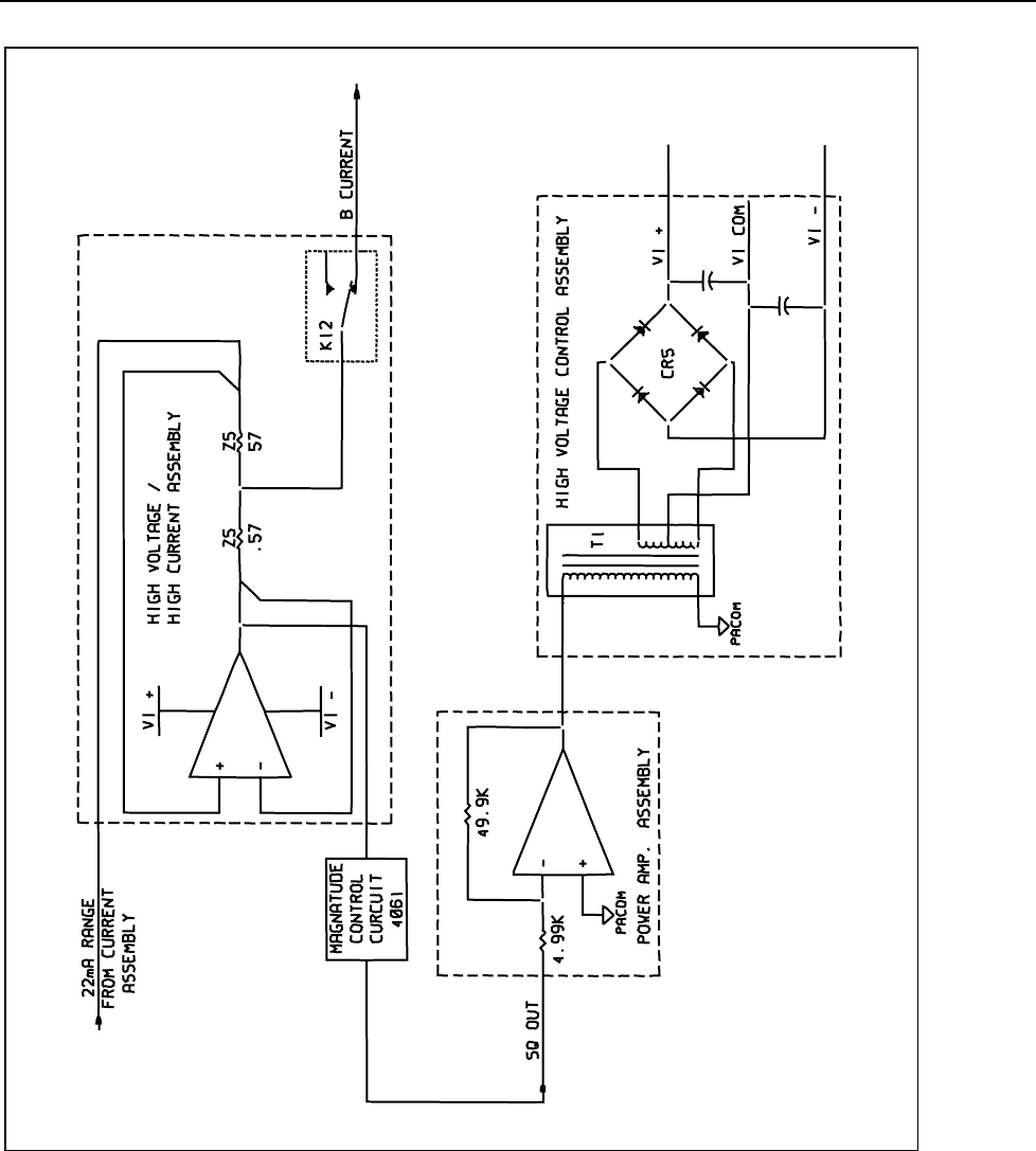
Theory of Operation
Analog Section Detailed Circuit Description
2
2-101
ahp024f.eps
Figure 2-27. High Voltage/High Current Assembly 2.2A AC and DC Ranges

5700A/5720A Series II Calibrator
Service Manual
2-102
Resistor network Z5 and hybrid H4 determine the performance of the 2.2A range.
Current from the A7 assembly develops a voltage across the 57W portion of Z5. The
2.2A current amplifier circuit forces the same voltage across the 0.57W portion of Z5.
Because the ratio of these resistors is 100, the current through 0.57W resistor is 100
times that coming from the Current assembly (A7). Relay K12 connects this 2.2A range
current to B CUR where it is routed to the Current assembly (A7), which provides the
proper relay switching to the front panel binding posts.
The 2.2A amplifier circuit contains the heater-controlled hybrid H4, op amps U3-U5,
and transistors Q11-Q16. This circuitry is outlined as detail 2 on sheet 2 of the High
Voltage/High Current assembly schematic. The H4 hybrid consists of an op amp
mounted on a heated substrate. The heater control circuit adjusts the base voltage of Q18
to deliver the proper power to the heater resistor. This maintains the hybrid at a constant
temperature in spite of environmental temperature variations. Transistor Q19 protects the
hybrid in case Q18 fails.
The output of the H4 hybrid is a voltage directly proportional to the current output G
OUT. Q22 and R72-R76 form a high-frequency path for loop stability. In the ac current
function, op amp U3A and its associated circuitry create a half-wave signal equal to the
positive peaks of the ac signal from H4. Resistor R47 keeps this half-wave signal
approximately 0.7V above 0V. This half-wave signal is then subtracted from the ac
signal coming from H4 by op amp U3B and its associated circuitry. This creates a half-
wave signal equal to the negative peaks of the ac signal from H4. Resistor R45 keeps this
half-wave signal approximately 0.7V below 0V. Transistor Q15 and resistor R50
generate a current from the negative peaks created by U3B. Transistor Q16 and R48
generate a current from the positive peaks created from U3A. The current from Q15 and
R50 develops a voltage across the 191Ω resistor (R69). This voltage is used by op amp
U4 which drives transistors Q11 and Q12 in the Darlington configuration for current
gain. Resistor R67 is the feedback path for U4. The voltage across 191Ω resistor R69 is
the same as across the 0.1Ω resistors R68 and R78. Since the value of R68 and R78 is
1000 times less than R69, the current through R68 is 1000 times greater. The current
from Q16 and R48 is increased by 1000, in the same manner as previously stated, with
op amp U5, resistors R56, R57, and R77, and Darlington-configured transistors Q13 and
Q14.
Only half of the circuitry is used, since the output current is either positive or negative in
the dc current function. When outputting a positive current, the voltage from H4 is
negative. Since there is no positive voltage, the output of U3A is zero, thus no current is
developed by R48 and Q16. At this time, the negative voltage from U3B generates an
output current in the same manner as in the ac current function. The opposite occurs
when outputting a negative dc current.
2-162. 2
.
2A Power Supply Filter Circuit
The 2A range power supply filter circuit on the High Voltage Control assembly (A14),
operating in conjunction with the Power Amplifier assembly (A16), generates the VI
±supplies used by the 2.2A amplifier circuit on the High Voltage/High Current assembly
(A15). The High Voltage Control assembly generates an amplitude controlled square
wave, HVCL, from the square wave generator and square wave amplifier circuits. This
HVCL is amplified by the Power Amplifier assembly (A16), which is set for a gain of
10. This amplified output, PA OUT DC, is connected to the primary side of transformer
T1 by relay K1. The stepped-down secondary voltage is full-wave rectified by CR5 and
filtered by C3 and C4 to generate the VI+ and VI- supplies respectively. VI± are low-
voltage, high current supplies. These supplies, along with the secondary center tap VI
COM, are routed to the High Voltage assembly.

Theory of Operation
Analog Section Detailed Circuit Description
2
2-103
VI+ supplies the output current when sourcing while VI- sinks it. To minimize power
dissipation, the magnitude of the VI± supplies is controlled to minimize the emitter to
collector voltage on the output stage transistors (Q11, Q14). This is done by controlling
the magnitude of the HVCL signal. The controlling function is described later in the
Magnitude Control theory.
2-163. High Voltage Digital Control
Digital control circuitry on the High Voltage Control assembly (A14) also contains the
control for the High Voltage/High Current assembly (A15). The heart of the digital
control circuitry is an 82C55 Programmable Peripheral Interface IC (U9), which is under
software control via the guarded digital bus. This IC has three ports which generate 24
outputs. These outputs are used to control four 5801 driver ICs (U10-U13), and an
analog multiplexer (U14) for self diagnostics.
All relays on both HV assemblies are controlled by drivers U10, U11, U12, and U13.
Driver U12 controls relays K14-K16, and generates seven control lines for controlling
various FETs and CMOS Analog Switch ICs contained on both assemblies. Port A
(PA0-PA7) of U9 provides a common input bus for all drivers. Port C (PC0-PC5) of U9
provides the strobe and enable lines for these drivers. Driver U10, which controls the
non-latching relays (K1-K6, K8-K13) on the High Voltage Control assembly, is strobed
by PC1. PC0 is inverted by U8C to provide the enable. Driver U11 controls latching
relay K7 on the High Voltage Control assembly and latching relays K1-K3 on the High
Voltage/High Current assembly. This driver is strobed by PC3. PC2 is inverted by U8D
to provide the enable. Driver U13, which controls the non-latching relays on the High
Voltage/High Current assembly (K4-K12 and K14), is strobed by PC5 and enabled in the
same manner as U10. Driver U12, which generates the Control Lines, is strobed by PC4
and enabled in the same manner as U10. Control line RST, from this driver, is inverted
by U8E to create PS OFF. This control line is used by the magnitude control circuit
described later.
The diagnostic circuit enables the Calibrator to monitor seven points on either the High
Voltage/High Current assembly (A15) or the High Voltage Control assembly (A14). A
4051 analog multiplexer (U14) is controlled by PB4-PB7 of port B of U9. This
multiplexer selects which one of these seven voltages are to be applied to the SDL line
where it is measured by the adc circuit on the DAC assembly (A11). HV MUX0-HV
MUX3 are points on the High Voltage/High Current assembly. HV MUX0 and HV
MUX1 monitor the oven temperature of the H4 and HR7 hybrids respectively. The
output of the dc HV amplifier/ac sense buffer circuit is divided by R18 and R19 to
generate HV MUX2. HV MUX3 monitors the current draw through the HV dc output
series pass circuit to detect an overcurrent condition in the high voltage dc mode.
Resistors R28 and R27 sense the current for a positive high voltage output and a negative
high voltage output respectively. MUX5-MUX7 are points on the High Voltage Control
assembly. MUX5 monitors the high voltage output. HV OUT is divided by R9-R13 and
R64.
This divided output is connected to the output peak measure circuit which uses op amp
U1B. In the dc V function, this circuit is a voltage follower. In the ac voltage function,
this circuit is a peak detector.
The output of U1B charges C5 with R17 being the discharge path. This provides a
positive dc voltage at MUX5. The output of the absolute value circuit is divided by R55
and R56 to generate MUX6. The output of the reference and error amplifier circuit is
divided by R46 and R47 to generate MUX7.

5700A/5720A Series II Calibrator
Service Manual
2-104
2-164. High Voltage Calibration
Refer to Figure 2-28 for the following discussion. The resistor network, (70 kΩ and 7
MΩ) which is part of the HR7 hybrid/resistor network assembly, determines the
accuracy of both 1100V ac and dc ranges. Calibration involves determining its offset and
gain constants.
To determine the offset, DAC outputs are connected to 70 kΩ input resistor by K1. The
output of the dc HV amplifier is inverted by U1 and its output is connected to the 7 MΩ
feedback resistor by K9, K8B, and K6. This configuration creates an inverting amplifier
with a gain of 100. Relay K9 connects the output of this amplifier to the RCL line, where
it is measured by the adc circuit on the DAC assembly (A11). The DAC’s adc circuit first
connects both its +input and -input to RCOM and takes a checkpoint reading. The +input
is then connected to the RCL line, which at this time is the amplifier output, and adjusts
the DAC output to obtain the same reading as the previous check point. This offset cal
constant is stored in nonvolatile memory.
To determine the gain, the High Voltage/High Current assembly is configured in the ac
1100V range, except PA SNS DC is connected directly to the 7 MΩ input resistor of the
ac sense buffer by relays K8 and K6 instead of going through step-up transformer T1.
The 6.5V reference (BRF6) is connected to the Power Amplifier assembly (A16) which
is configured for an inverting gain of 20 to create a -130V output. The ac sense buffer
circuit attenuates this signal by 100 to generate 1.3V at its output. This 1.3V is connected
to the RCL line by relay K2 where it is connected to the +input of the adc circuit on the
DAC assembly. DAC OUT HI, which is connected to the -input, is adjusted until a null
is achieved. The gain can be determined by using this and the previous offset reading.
This determines the exact ratio of 70 kΩ and 7 MΩ resistor network on the HR7
assembly. This known ratio can then be used to output very accurate dc voltages in
1100V dc range.
2-165. Calibration of the AC Function
The HR7 resistor network, previously calibrated at dc, is further characterized for its
frequency response. The Calibrator is placed in the ac 1100V range, except with HV
OUT and HV SENSE tied by relay K11 on the High Voltage/High Current assembly
(A15) instead of being tied at the load. The Oscillator Output assembly is set so the
output of the High Voltage/High Current Voltage assembly is approximately 695V at
130 Hz. This high voltage output (INT HV SNS) is connected to the AC CAL line,
through 399.6 kΩ resistor Z6, by relays K10 and K8A on the High Voltage assembly.
The AC CAL signal is routed to the Oscillator Control assembly (A12) where it is
measured by a 400Ω rms sensor.
Since the voltage is approximately 700V and it is applied through a 399.6 kΩ resistor
(Z6) to the 400Ω rms sensor, approximately 1.75 mA of current flows through the rms
sensor on the Oscillator Control assembly. A dc reading of the sensor, which is
approximately 0.7V (1.75 mA x 400Ω), is taken and then stored in memory with the
Oscillator Output level.
The Oscillator Output frequency is then increased to 500 Hz. The Oscillator Output level
is adjusted so the dc reading from the rms sensor is the same as for 130 Hz, and stored in
memory. This step is again repeated at 1 kHz. This characterizes the HR7 resistor
network’s frequency response. An accurate ac voltage can now be obtained at any
frequency between 50 Hz and 1 kHz. The theory of operation for the rms sensor is
contained in the Oscillator Control (A12) theory.
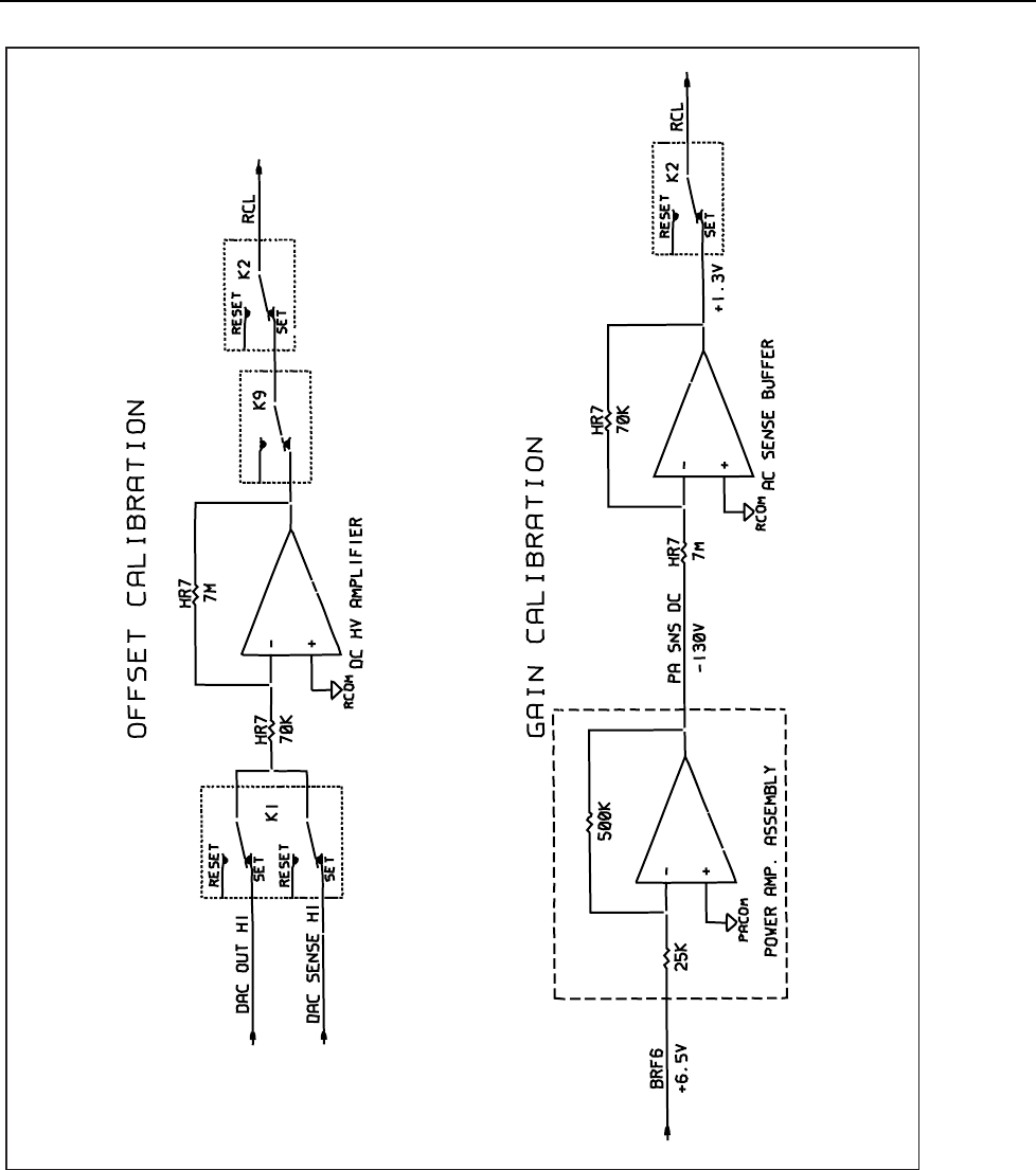
Theory of Operation
Analog Section Detailed Circuit Description
2
2-105
ahp025f.eps
Figure 2-28. High Voltage/High Current Assembly Calibration

5700A/5720A Series II Calibrator
Service Manual
2-106
2-166. Calibration of the Current Function.
Refer to Figure 2-29 for the following discussion. The resistor network Z5 determines
the accuracy of the 2.2A current range. Calibration involves determining its offset and
gain constants. The Calibrator is configured as in the 2.2A dc function, except that the
Current assembly (A7) is set to the 2.2 mA range.
To determine offset, the output (B CUR) is routed back to the Current assembly where it
is connected to INT OUT HI. INT OUT HI is routed to the Ohms Main assembly (A10),
where it is connected to a previously calibrated 10Ω resistor. The voltage generated
across this 10Ω resistor is routed to the differential amplifier on the Ohms Cal assembly
(A9). The output of the differential amplifier is routed to the DAC assembly (A11)
where it is measured by its adc circuit. A checkpoint reading is first taken by removing
INT OUT HI from the 10Ω resistor and measuring the voltage across the resistor. The
offset is then measured by connecting INT OUT HI to the 10Ω resistor. The DAC
assembly, which controls the output of the Current assembly, is adjusted until the adc
circuit measures the same as the previous checkpoint reading.
To determine gain, the Calibrator is configured as in the previous step, except with the
Current assembly outputting 1.3 mA generated from the 13V reference (BRF13 and
BSRF13) from the DAC assembly. This 1.3 mA is amplified 100 times by the 2.2A
amplifier. The resulting 130 mA is connected to the 10Ω resistor on the Ohms Main
assembly by the same path as for the offset calibration. The resulting 1.3V across this
10Ω resistor is routed to the Ohms Cal assembly (A9), where it is connected to the -input
of the differential amplifier. The +input of the differential amplifier is connected to the
output of the DAC assembly. The output of the differential amplifier is connected to the
RCL line which is routed to the adc circuit on the DAC assembly. The DAC output,
which is the +input of the differential amplifier, is adjusted until a null is measured on
the RCL line by the DAC’s adc circuit. This step is repeated by changing the -input of
the differential amplifier to the other side of the 10Ω resistor. The software now
computes the exact voltage drop across the 10Ω resistor. Gain is determined by using
this and the previous offset reading.
2-167. High Voltage Magnitude Control
The square wave (HVCL) used in the previously described functions, is created and
amplitude controlled by the High Voltage Control assembly (A14). This circuitry, shown
on sheet 2 of the schematic, contains the absolute value circuit, signal/polarity selection
circuit, reference and error amplifier, square wave generator, and the square wave
amplifier.
The absolute value circuit contains op amp U2A, U2B, Q3, diodes CR8 and CR9,
capacitor C20, and resistors R27-R32 and R68. During operation in the ac current
function, this circuit creates an absolute value of the G OUT signal from the collectors of
the 2.2A output transistors. Op amp U2A generates a negative half-wave signal equal to
the positive peaks of G OUT. Resistors R32 and R27 sum this half-wave signal and the
input signal G OUT at the input of U2B. Capacitor C20 averages the voltage so the
output of U2B is a dc voltage which represents the positive peak voltage of G OUT. In
the high voltage dc function, the 2.2A amplifier circuit is not used, so the output of U2B
is 0V.

Theory of Operation
Analog Section Detailed Circuit Description
2
2-107
ahp026f.eps
Figure 2-29. High Voltage/High Current Assembly 2.2A Range Calibration

5700A/5720A Series II Calibrator
Service Manual
2-108
The signal/polarity selection circuit generates the ERROR SIGNAL used by the error
amplifier. It contains op amp U2C, CMOS analog switch U6, and resistor R35-R39.
Control line V/I controls U6B and U6C which select the VI± when in the current mode.
Control lines ±* and ± control U6A and U6D respectively. These switches, operating in
conjunction with U6B and U6C, select between VI±, -SP C or +SP C. In the current
function, U2C subtracts the power supply voltage (VI±) from the absolute voltage
created by the absolute value circuit to create ERROR SIGNAL. This gives a measure of
the emitter to collector voltage of the driving device for each operating function. In the
positive dc voltage function, U2C is configured as a unity-gain inverting op amp. In the
negative dc voltage function, U2C is configured as a voltage follower.
The reference and error amplifier circuit contains op amp U2D, CMOS analog switch
U7B, zener diode VR1, transistors Q2 and Q4, diodes CR10-CR11, capacitor C18, and
resistors R40-R45. Zener diode VR1, R40-R45, Q4, and U7B create a reference voltage.
Control line V/I controls U7B which switches R43-R45 in or out to change this reference
voltage value, depending on the operating function. In the HV dc range, R40 and R41 are
used, balancing the error amplifier with the ERROR SIGNAL near 6.8V. In the 2A dc
range, U7B and Q4 are on, R43 is paralleled with R41, and R45 is paralleled with R40,
so the error amplifier balances when the ERROR SIGNAL is near 3.1V. In the 2A ac
function, Q4 is off, R44 is in series with R45, so the error amplifier balances when the
ERROR SIGNAL is about 5.2V. The output of U2C, ERROR SIGNAL, is summed with
the reference voltage by R40 and R41. This voltage is connected to the error amplifier
U2D which, with C18, is configured as an integrator. The error amplifier generates the
signal AMPLITUDE, which dynamically controls the amplitude of the square wave.
This AMPLITUDE is connected to the input of U7C. -AMPLITUDE, provided by
inverting op amp U1A, is connected to the input of U7D. Control line PS OFF provides a
soft start of the error amplifier. With this line high, Q2 is turned on, shorting C18, which
sets the AMPLITUDE control line to 0V. Once the High Voltage/High Current assembly
is set up for proper operation, this line goes low to turn off Q2.
The square wave generator circuit creates a 1 kHz signal QSQB and its complement
QSQB*. These signals are generated by R26, C17, and a stable multivibrator U4.
Control line FREQ controls the CMOS analog switch U7A, which parallels R25 to R26.
This changes the frequency of oscillation to prevent beating when putting out 2A ac near
1 kHz. Control line PS OFF goes high to shut down this oscillator when its not required.
The square-wave amplifier contains op amp U3 and CMOS analog switches U7C and
U7D. Switch U5C is connected to the AMPLITUDE voltage and is controlled by QSQB
from the square wave generator. Switch U7D is connected to AMPLITUDE through
inverting op amp U1A and is controlled by QSQB* from the square wave generator. The
input signal to the square wave amplifier is the output of U7C and U7D. Since QSQB* is
the complement of QSQB, the resulting square wave has a positive peak equal to
AMPLITUDE, and a negative peak equal to -AMPLITUDE. This square wave is
amplified by U3, which is configured for a gain of 2.6, to create HVCL. HVCL is the
square-wave signal used by the Power Amplifier assembly in the previously described
functions.
2-168. Ohms Overview
The Ohms function for the Calibrator is provided by two plug in circuit boards, the
Ohms Main assembly (A10) and the Ohms Cal assembly (A9). These two assemblies
function as one to supply fixed values of resistance from 1Ω to 100 MΩ. Resistance
output is available in values of 1x10n (1, 10, 100, 1k ... 100M) and 1.9x10n (1.9, 19, 190,
... 19M) from short to 100 MΩ. After the ohms function is calibrated, the Output Display
shows the true value of the resistance selected.

Theory of Operation
Analog Section Detailed Circuit Description
2
2-109
These assemblies are also used to calibrate the Calibrator Current function. The Ohms
Main assembly contains all the resistor values except the 1Ω, 1.9Ω, and short, which are
located on the Ohms Cal assembly. It also contains the relays and their drivers to switch
these values as requested under program control.
The Ohms Cal assembly contains all calibration circuits except for one op amp on the
Ohms Main assembly. It also contains a circuit to provide accurate calibration of two-
wire ohmmeters. In addition, there are relays, relay drivers, and logic to interface the
Ohms assemblies to the digital bus. Refer to Figure 2-30 for a simplified schematic of
both the Ohms Main and Ohms Cal assemblies.
2-169. Ohms Main Assembly (A10)
The Ohms Main assembly uses three Fluke hermetically-sealed thin film resistor
networks (Z1, Z2 and Z3) to obtain values from 10Ω to 19 MΩ. The values are arranged
in two strings, one for decade values and the other for the multiples of 1.9. The 100 MΩ
value is achieved by inserting a 90 MΩ film resistor (R1) in series with the decade
string.
2-170. Selection of Resistance Values
Refer to Figure 2-31 for the following discussion. Relays select the resistance values. All
resistor values have four-wire connections except 100 MΩ, which is two-wire. The
output high and sense high side of a resistance value is connected to INT OUT HI and
INT SENSE HI by relays K1 and K2 in the reset position, except 100 MΩ, which is
connected to INT OUT HI by K5. Relays on the motherboard connect INT OUT HI and
INT SENSE HI to the OUTPUT HI and SENSE HI binding posts.
The low side of the 1x string is connected to OHMS SENSE LO and OHMS OUT LO by
relay K27 (A and B) in the reset position. The low side of the 1.9x string is connected to
the same lines by relay K39 (A and B). These lines are routed to the Ohms Cal assembly
where they are connected via relays to the OUTPUT LO and SENSE LO binding posts.
The 10 MΩ value is selected by K7 (reset) and K8 (energized) and the 1 MΩ value by
K9 and K10 (reset). Selection of decades below 1 MΩ is done by K15 and K16 (reset)
plus a pair of relays from K17 through K26A. For example, to select 10 kΩ, relays
K18A and K20A are reset.
The 19 MΩ value is selected by K11 and K12 (energized), and the 1.9 MΩ value by K13
and K14 (reset). Selection of 1.9 decades below 1.9 MΩ is done by K35 and K36 (reset)
plus a pair of relays from K18B through K26B and K37.
Two lines, OHMS OUT HI and OHMS SENSE HI, are brought over to the Ohms Cal
assembly to connect to 1Ω, 1.9Ω, and short. These lines also access resistance values
during calibration. Relay K29 connects OHMS OUT HI to the 1x10n string when set, and
to the 1.9x10n string when reset. Relay K30 connects OHMS SENSE HI to the 1.9x10n
string during calibration.
Relays K3, K28, K31-K34, and op amp U1 and its associated components are only used
during calibration. Operation of this circuitry is described in the "Calibration" part of the
Ohms Cal theory.
Relays K4 and K6 are used during two-wire compensation. This is described in the
"Two-Wire Compensation" part of the Ohms Cal theory.
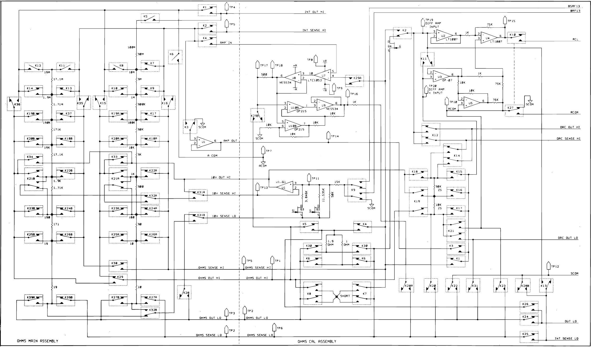
5700/5720A Series II Calibrator
Service Manual
Figure 2-30. Ohms Assemblies Simplified Schematic ahp38f.eps
2-110
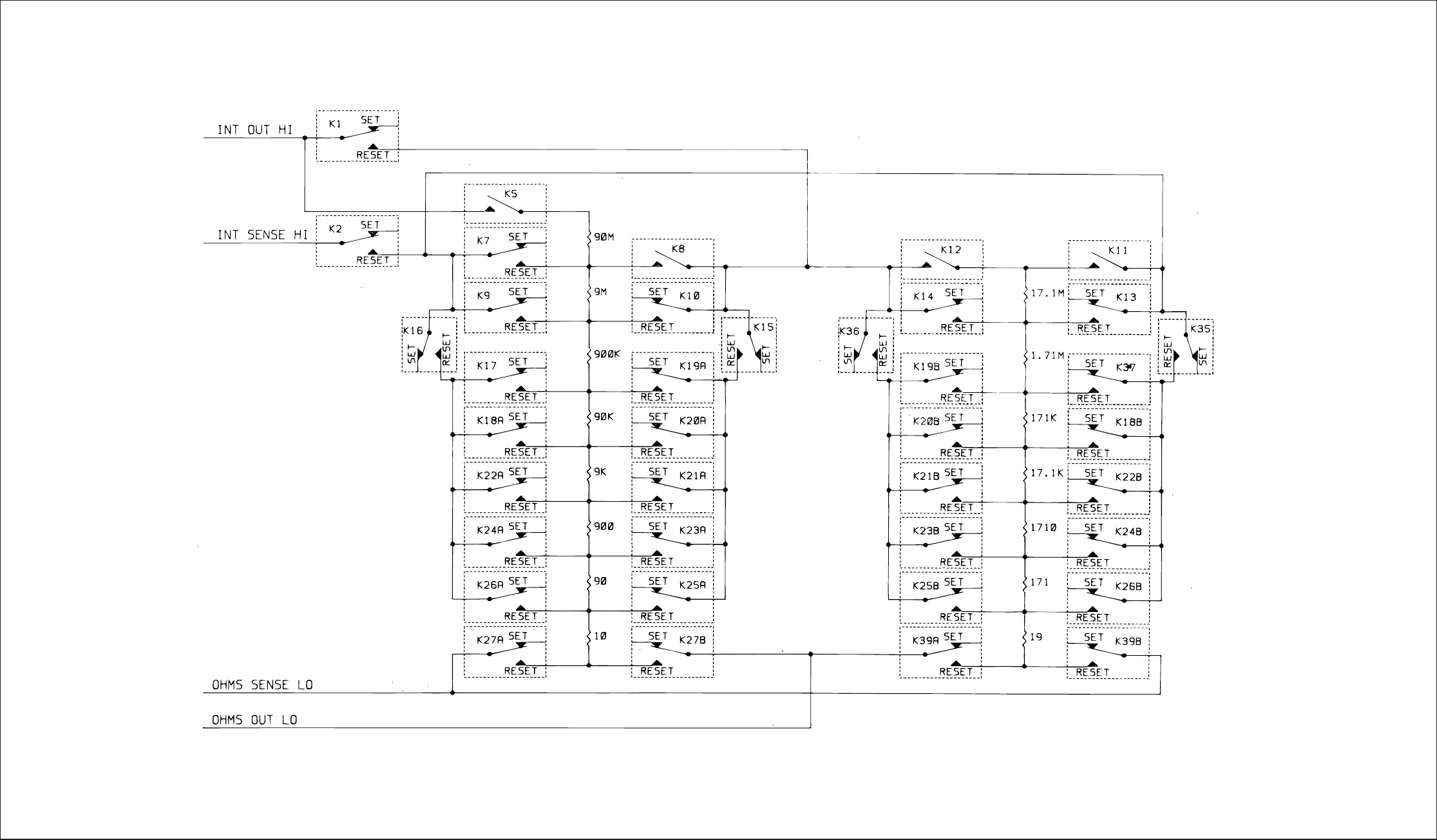
2
Theory of Operation
Analog Selection Detailed Circuit Description
ahp39f.eps
2-111
Figure 2-31. Ohms Main Assembly Simplified Schematic

5700A/5720A Series II Calibrator
Service Manual
2-112
2-171. Ohms Main Assembly Support of Current Function Calibration
To calibrate the current function, the Current assembly routes output current to the Ohms
Main assembly, where it is connected through a resistance. Current is determined by
measuring the voltage across this resistance. During calibration, half of K38 connects
DAC OUT LO to the SENSE LO side of the 1x10n string (Z1 pin 6). The Current
assembly generates approximately 60 µA of current on the DAC OUT LO line, which
can cause an error during measurement. To prevent this error, half of relay K38 connects
the -17S supply through R6 to the DAC OUT LO line. This generates an opposite-
polarity 60 µA current to cancel the current from the Current assembly.
2-172. Ohms Digital Control
The Ohms Main assembly is digitally controlled by the 82C55 Programmable Peripheral
Interface IC on the Ohms Cal assembly. This IC, under system software control through
the guarded digital bus, has three ports generating 24 outputs. PA0-PA7 of port A, PB0-
PB3 of port B, and PC0-PC4 of port C are routed on the motherboard to the Ohms Main
assembly. These lines and two decoders in U9 and U10 control nine relay driver ICs,
which in turn control 39 Ohms relays. Relay driver U3 drives non-latching relays K5,
K6, K8, K11, K12 and K38. Relay drivers U2, U5-U8, and U11-U13 drive the latching
relays.
Port A (PA0-PA7) is a common input bus for all relay drivers. IC U9 decodes PB0-PB3
to strobe the latching relay drivers. This signal causes the contents of the data on the
input bus to be latched into the latch portion of the selected device. IC U10 decodes
PC0-PC3 to provide four enable lines. Each line goes to two latch/drivers and when true
(0V), drives the relay coils on or off according to the contents of the latch. Since these
are latching relays, they are pulsed only briefly. The latching relays each have two coils,
one to set the relay and one to reset it. When the ohms function is not being used, all
relays are set, as shown on the schematic.
PC4 is the strobe line for non-latching relay driver U3. The enable is connected to LH
COM so the relays receive constant drive. These non-latching reed relays are shown in
the non-energized state.
2-173. Ohms Cal Assembly (A9)
The Ohms Cal assembly (A9) contains the 1Ω, 1.9Ω, and short resistance values. It also
contains a digital control circuit, and a two-wire compensation circuit to allow accurate
calibration of two-wire ohmmeters. A differential amplifier circuit and a 2/5/10V source
circuit are used during calibration of the ohms function.
2-174. Ohms CAL Digital Control
The heart of the Ohms Cal assembly digital control circuit is the 82C55 Programmable
Peripheral Interface IC (U11) mentioned previously under "Digital Control". This IC has
three ports generating 24 outputs. These outputs control seven 5801 latching relay
drivers ICs (U14-U20), a 4051 analog multiplexer (U21) for self diagnostics, and several
FET switches.
Port A (PA0-PA7) is a common input bus for latching relay drivers and multiplexer U21.
These lines also go to the Ohms Main assembly as previously described to control relay
drivers there.
Lines PB0-PB3 of port B goes to decoder U12 (PB3 is inverted by U22) and to the Ohms
Main assembly. The output of U12 strobes latch/driver ICs to latch data on input bus
lines.

Theory of Operation
Analog Section Detailed Circuit Description
2
2-113
Lines PC0-PC3 of port C go to decoder U13 and to the Ohms Main assembly. Decoder
U13 enables two latch/driver ICs at a time. Setting the enable true (0V) causes the relay
coils to be driven on or off depending on the contents of the latch portion of the selected
ICs. Since these are latching relays, they are pulsed only briefly.
The outputs PB4, PB5 and PB6 of U11 are connected to the gates of FETs Q2, Q3 and
Q4 respectively. The Programmable Peripheral Interface IC turns them on for a one (5V)
and off for a zero (0V). PB7 is connected to the base of Q6 through R31. When PB7 is
true (5V), it turns on Q6, which turns on Q5, which in turn supplies +17S to U6. PC4
goes to the Ohms Main assembly where it strobes relay latch/drivers for the non-latching
relays.
Line PC6 goes to the diagnostic circuit where it enables and disables output from the
multiplexer (U21). Connected to the input of the multiplexer are five voltage dividers
made from resistors in Z3 and Z4.
Two inputs to these dividers are connected. One is 10V OUT HI from the 2/5/10V
source circuit. The other is 2W COMP from the two-wire compensation circuit. These
inputs are connected to the SDL line by the multiplexer, where they are routed to the adc
circuit on the DAC assembly and measured during calibrator diagnostics. PC7 is not
used.
2-175. 1
,
1
.
9
,
and Short Resistance
Although located on the Ohms Cal assembly, the 1Ω value, 1.9Ω value, and short
operate as part of the Ohms Main assembly, filling out the range of values available to
the operator. The 1Ω value is made of four 4Ω wirewound resistors in parallel (R41).
The 1.9Ω value is made of two 3.8 ohm wirewound resistors in parallel (R42). Relays
K4 and K5 connect the 1 ohm and 1.9Ω values to OHMS OUT HI and OHMS SENSE
HI. Relays K6 and K30 connect them to OHMS OUT LO and OHMS SENSE LO.
Relays K7 and K8 select the short.
The Ohms Cal assembly contains the relays that switch the low side of the selected
resistance onto the output bus. (High sides are connected to the output bus by relays on
the Ohms Main assembly.) Relay K24 connects OHMS OUT LO to OUT LO and K25
connects OHMS SENSE LO to INT SENSE LO.
2-176. Two-Wire Ohmmeter Compensation Circuit.
Refer to Figure 2-32 for the following discussion. The Ohms Cal assembly contains a
two-wire lead drop compensation circuit that allows accurate calibration of two-wire
ohmmeters. The error normally encountered when calibrating a two-wire ohmmeter is
due to the voltage drop in the path resistance between the meter and the calibration
resistor. This circuit reduces the voltage drop to an insignificant level. Two wire
compensation can be used only with ohm meters that source continuous (not pulsed) dc
current.
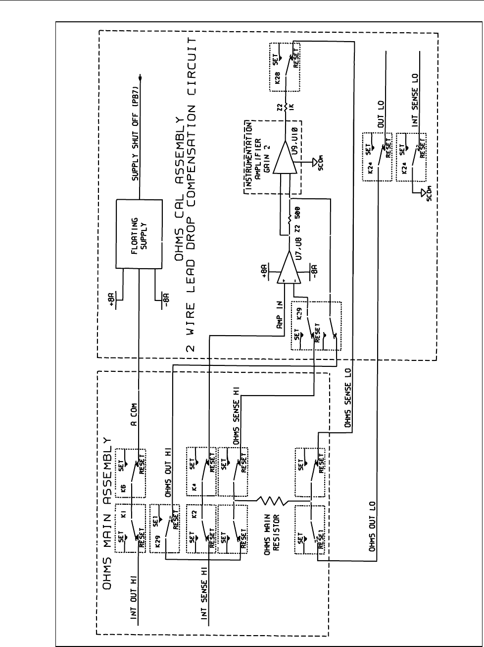
5700A/5720A Series II Calibrator
Service Manual
2-114
ahp027f.eps
Figure 2-32. Two-Wire Lead Drop Compensation Circuit

Theory of Operation
Analog Section Detailed Circuit Description
2
2-115
2-177. Two-Wire Compensation Power Supplies
The floating supplies for U7 and U8 consist of a dc-to-dc converter made up of U6, T1
and associated components. Switching-regulator control IC U6 switches +17S through
the primary of T1 at about 30 kHz as determined by R27 and C21. The switching creates
high-frequency spikes on the +17S line which are filtered out by L2, R25, C18, C19,
C20, and C52. When the two-wire compensation circuit is not in use, control line PB7
turns Q5 and Q6 off, which removes +17S, switching off U6. The secondary of T1 is
rectified and filtered by CR1, CR2, CR9, CR10, C22, and C23. The voltage is then
regulated by 8.2V zener diodes VR1 and VR2. Additional filtering is provided by L3,
L4, R43, R44, C24, and C25. Two capacitors (C53 and C54) between A COM and S
COM reduce switching noise that would otherwise appear across the calibration resistor.
2-178. High Side Cancellation
The high side voltage drop is eliminated by U7 and U8. Chopper-stabilized op amp U7
and buffer amplifier U8 supply up to 10 mA. The current from the high side of the
ohmmeter being calibrated enters at the OUTPUT HI binding post, goes through K1 and
K6 on the Ohms assembly, and is routed to the Ohms Cal assembly where it connects to
A COM. The A COM connection is a common for the floating supply that powers U7
and U8. The current then flows out of U8 through 500Ω in Z2 and through K29 to the
calibration resistor via the OHMS OUT HI line.
K29 connects the -input of U7 to the sense point of the calibration resistance via OHMS
SENSE HI. Relays K2 and K4 on the Ohms Main assembly connect the +input of U7,
AMP IN, to INT SENSE HI. Relays on the motherboard connect INT SENSE HI to the
OUTPUT HI or SENSE HI binding post. Connected this way, U7 controls the voltage at
the output of U8 so that the voltage at the input of U7 stays zero. This forces the voltage
drop in the path to zero. Diodes CR3-CR6 and resistor R45 provide protection for U7.
2-179. Low Side Cancellation
The voltage drop in the low side path is canceled by current from high current op amp
U9. U9 is driven by dual FET input op amp U10. The two non-inverting inputs of U10
are connected across the 500Ω resistor in Z2. This enables U10, in conjunction with the
four 10 kΩ resistors in Z2, to sense the current in the high side path and to supply
(through U9 and the 1 kΩ resistor in Z2) a current equal but opposite to the current
through the low side path. This cancels the drop in that path. This canceling current goes
through relay K28A to the low sense point of the calibration resistor via OHMS SENSE
LO. From there it goes through the output low path to the OUTPUT LO binding post and
then through the sense low path back to the Ohms Cal assembly and through K28B to S
COM.
2-180. Ohms Calibration
The remaining circuitry is used only for calibration of the resistor values. All values
except 1Ω and 1.9Ω are calibrated using a single external 10 kΩ resistance standard
connected to the binding posts. The 1Ω and 1.9Ω values are calibrated using an external
1Ω standard. How to do the procedure is described in Section 7 of the Operator Manual.
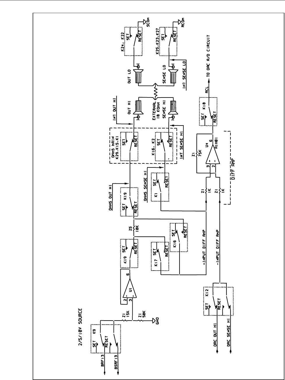
5700A/5720A Series II Calibrator
Service Manual
2-116
ahp028f.eps
Figure 2-33. Calibration to an External 10 kΩ Standard

Theory of Operation
Analog Section Detailed Circuit Description
2
2-117
2-181. Calibrating to the External 10 KW Standard
Refer to Figure 2-33 for the following discussion. The first step in ohms calibration is to
compare the 10 kΩ standard against the 10 kΩ value on the Ohms Cal assembly. This is
done by passing a current through both values and measuring the voltage drop across
each. The ratio of the voltages is equal to the ratio of the resistances.
The source of current comes from the 2/5/10V source circuit, which contains U1, Q1,
Q2, Q3 and Z1. The buffered 13V reference voltage from the DAC assembly (A11) is
switched through K9 to a voltage divider made up of resistors in Z1.
To calibrate the 10 kΩ resistance, control lines PB4 and PB5 turn off FETs Q2 and Q3
respectively. In this mode, the output of the divider uses the 15 kΩ and 50 kΩ values to
produce an output of 10V. This voltage is buffered by U1 and Q1. The current from this
source, 10V OUT HI, is sent through K19 to one side of the 10 kΩ resistance in Z5. 10V
SENSE HI is connected to 10V OUT HI by K31A on the Ohms assembly. The other side
of the 10 kΩ resistance in Z5 is connected to OHMS OUT HI by K19. This is routed to
the Ohms Main assembly where is goes through K29, K15 and K1 to INT OUT HI,
which is connected to the OUTPUT HI binding post by relays on the motherboard. From
there it goes through the external 10 kΩ standard and back in through the OUTPUT LO
binding post and over to the Ohms Cal assembly where it connects to S COM through
K24 and K22.
The voltage drops are measured by comparing each voltage to the DAC assembly output
in a differential amplifier circuit made of U2 through U5.
Since the DAC and differential amplifier are referenced to R COM, this line is brought
out through K27, K23 and K25 to INT SENSE LO. This is connected to the SENSE LO
binding post (which is connected to the sense low point of the standard). Line DAC OUT
LO is tied to S COM by relay K31. The high side of the DAC, DAC OUT HI and DAC
SENSE HI, are tied together and connected by K12 to U2, which is the differential
amplifier -input.
The voltage to be measured is connected to U3, which is the differential amplifier
+input. The output of U2 and U3 goes to U4 through gain setting resistors in Z1. These
set the gain of the differential amplifier to 75. The differential amplifier generates a
current through the 1 kΩ (pins 1-2) and 75 kΩ (pins 2-3) resistors in Z1 to R COM. This
current on R COM can cause an error during measurement. Op amp U5, configured as an
inverting amplifier, generates an equal current of opposite polarity through 76 kΩ
resistor R18 to cancel the current from the differential amplifier. The output of U4 goes
through K10 to the RCL line. This line is connected to the DAC assembly, where it goes
through an amplifier to the adc circuit.
The calibration program uses the adc circuit to measure the differential amplifier output
voltage. First the differential amplifier offset voltage is determined. (This offset is
different for each input condition.) Readings are taken to determine each offset voltage
by checking the output of the differential amplifier at equal voltages on the inputs. This
is done by switching K11 to the reset position to connect the differential amplifier +input
and -input together, then measuring the output with the DAC’s adc circuit.
Once the offsets are known, the software determines the calibration voltages by
adjusting the DAC output until the adc reading is the same as the offset. At that point,
the DAC output equals the voltage being measured.
Three readings are required to determine the ratio of the two resistances. For the first
reading, K16 connects the differential amplifier +input to the 10 kΩ resistor in Z5. For
the second reading, K17 connects the +input to the other side of that resistor. Subtracting
the first reading from the second gives the voltage across the internal 10 kΩ. For the
third reading, K1 on the Ohms Cal assembly connects the + input to OHMS SENSE HI.

5700A/5720A Series II Calibrator
Service Manual
2-118
OHMS SENSE HI is connected to INT SENSE HI by K16 and K2 on the Ohms Main
assembly. INT SENSE HI is connected to the SENSE HI binding post by relay K2 on the
motherboard which is the sense high side of the 10 kΩ external standard. The ratio of
this third reading to the difference of the first two readings is proportional to the ratio of
the two resistances. Thus by knowing the resistance of the external standard, the
software can calculate the value of the internal 10 kΩ resistance value.
2-182. Calibrating 10 KW and 19 KW
The next step in calibrating the ohms function is to determine the 10 kΩ and 19 kΩ
values on the Ohms Main assembly. This is done just like the 10 kΩ value on the Ohms
Cal assembly, except the 10 kΩ resistance on the Ohms Cal assembly acts as the
standard and is placed in series with 10 kΩ or 19 kΩ on the Ohms assembly.
This is done using K19 on the Ohms Cal assembly and K29, K20A and K27 on the
Ohms Main assembly for the 10 kΩ, and K29, K20B and K39 for the 19 kΩ value. The
source on the Ohms Cal assembly again outputs 10V. Again three readings are taken.
The first and second are the same as previously described. For the third reading, the
differential amplifier +input is connected through K1 on the Ohms Cal assembly and
through K18A on the Ohms Main assembly for 10 kΩ and K30 and K18B for 19 kΩ.
The software then calculates the 10 kΩ and 19 kΩ values using the ratio of readings and
the known value of the 10 kΩ on the Ohms Cal assembly.
2-183. Calibrating 100 KW
Once the 10 kΩ value is determined, the 100 kΩ value is calibrated by comparing its
value against 10 kΩ. The 10V source is connected across 100 kΩ. Since the 10 kΩ
resistance is used as part of 100 kΩ, the current goes through both.
Relays K33 and K19A on the Ohms Main assembly connect 10V OUT HI to 100 kΩ.
Relays K23 and K27 on the Ohms Cal assembly connects OHMS SENSE LO to RCOM.
OHMS OUT LO, DAC OUT LO, and 10V SENSE LO are connected to SCOM. Relay
K22 on the Ohms Cal assembly connects OHMS OUT LO to SCOM. OHMS OUT LO is
connected to DAC OUT LO by K31 on the Ohms Cal assembly, and to 10V SENSE LO
by K31B and K28 on the Ohms Main assembly.
Only two readings are required because this time there is no path resistance to subtract
out. DAC OUT HI and DAC SENSE HI are tied together and connected to the -input of
the differential amplifier by relay K12.
For the first reading, the +input of the differential amplifier is connected to the sense
side of the 100 kΩ point in the string through K1 on the Ohms Cal assembly and K17 on
the Ohms Main assembly. For the second reading, the + it is connected to the 10 kΩ
point by K18A. The software calculates the 100 kΩ value from the ratio of the readings
and the known 10 kΩ value.
2-184. Completion of High Resistance Value Calibration
Once 100 kΩ is determined, 1 MΩ and the other values up to 100 MΩ are determined in
a similar way. Using the same techniques, 190 kΩ is calibrated against 19 kΩ, and so
forth up to 19 MΩ.
Too much current noise is generated by U3 in the differential amplifier circuit for
accurate calibration of resistances above 1 MΩ. For these values, U1 on the Ohms Main
assembly (a low-bias current FET op amp) is switched ahead of U3.
The 1 kΩ and 1.9 kΩ resistance values are determined from the 10 kΩ and 19 kΩ
respectively.

Theory of Operation
Analog Section Detailed Circuit Description
2
2-119
The 10Ω, 19Ω, 100Ω and 190Ω resistance values are determined using 2V from the
2/5/10V source and using internal 10:1 divider (Z5) in conjunction with the DAC. To get
2V, Q2 and Q3 are both turned on, which parallels both the 11.535 kΩ value and the
3.846 kΩ value with the 50 kΩ value. The lower voltage is required to lower the power
dissipation in the resistors.
Using 2V presents a problem for the DAC. Instead of working at 10V and 1V, it would
be working at 2V and 0.2V. This level is too low to get accurate results from the DAC.
To solve this problem, the DAC is used only at 2V and the 0.2V level is achieved using a
10:1 divider. The DAC calibrates this 10:1 divider at 10V and 1V. The divider is made
of a 90 kΩ and a 10 kΩ resistor in Z5. To calibrate the divider, 10V is applied to the top
of the divider through K18. The low side of the divider is connected to R COM (K21 and
K27), DAC OUT LO (K21) and S COM through K20 on the Ohms Cal assembly,
K27A/B on the Ohms Main assembly and K22 on the Ohms Cal assembly. Two readings
are taken. Their ratio is equal to the division ratio of the divider. The -input of the
differential amplifier is connected to the DAC output by K12. For the first reading, K15
connects the top of the divider to the +input of the differential amplifier. For the second
reading, K16 connects the divider point to the +input of the differential amplifier. The
exact ratio of this divider can now be determined by these two readings.
Refer to Figure 2-34 for the following discussion. To calibrate the 10Ω resistor, the DAC
output is connected to the top of the divider by K14. The 2V source is connected across
100Ω on the Ohms Main assembly. This is done by 10V OUT HI, set to 2V, connected
to the high side of the 100Ω string by K33 and K23A on the Ohms Main assembly. Line
10V SENSE HI is also connected to this point by K31A and K32A on the Ohms
assembly. Line OHMS OUT LO and OHMS SENSE LO are connected to the low side of
the 100Ω string by K27B and K27A respectively. Line OHMS OUT LO is connected to
SCOM by K22 on the Ohms Cal assembly and is also connected to 10V SENSE LO by
K32B and K31B on the Ohms Main assembly. OHMS SENSE LO is connected to the
low side of the internal divider by K20 on the Ohms Cal assembly. The Ohms Cal
assembly also connects RCOM to the low side of the divider by K27 and K21. Relay
K21 also connects this point to DAC OUT LO.
Two measurements are taken. The first is with the +input of the differential amplifier
connected to the DAC output through K15. The - input is connected to the sense point of
the 100Ω resistance by K24A on the Ohms Main assembly and K2 on the Ohms Cal
assembly. The DAC is adjusted until its value is the same as the voltage across 100Ω.
Then the inputs of the differential amplifier are moved. The +input is connected to the
divider output on the Ohms Cal assembly by K16. The - input is connected to the sense
point of the 10Ω resistance by K26A on the Ohms Main assembly and K2 on the Ohms
Cal assembly. The DAC is again adjusted until the voltages are equal. The differential
amplifier sees 0.2V on each input for this measurement but the DAC is at 2V. The value
of 10Ω is determined from the two DAC settings and the division ratio of the divider on
the Ohms Cal assembly. The same procedure is used to determine the 100Ω value from
the 1 kΩ value, the 190Ω value from the 1.9 kΩ value and the 19Ω value from the 190Ω
value.
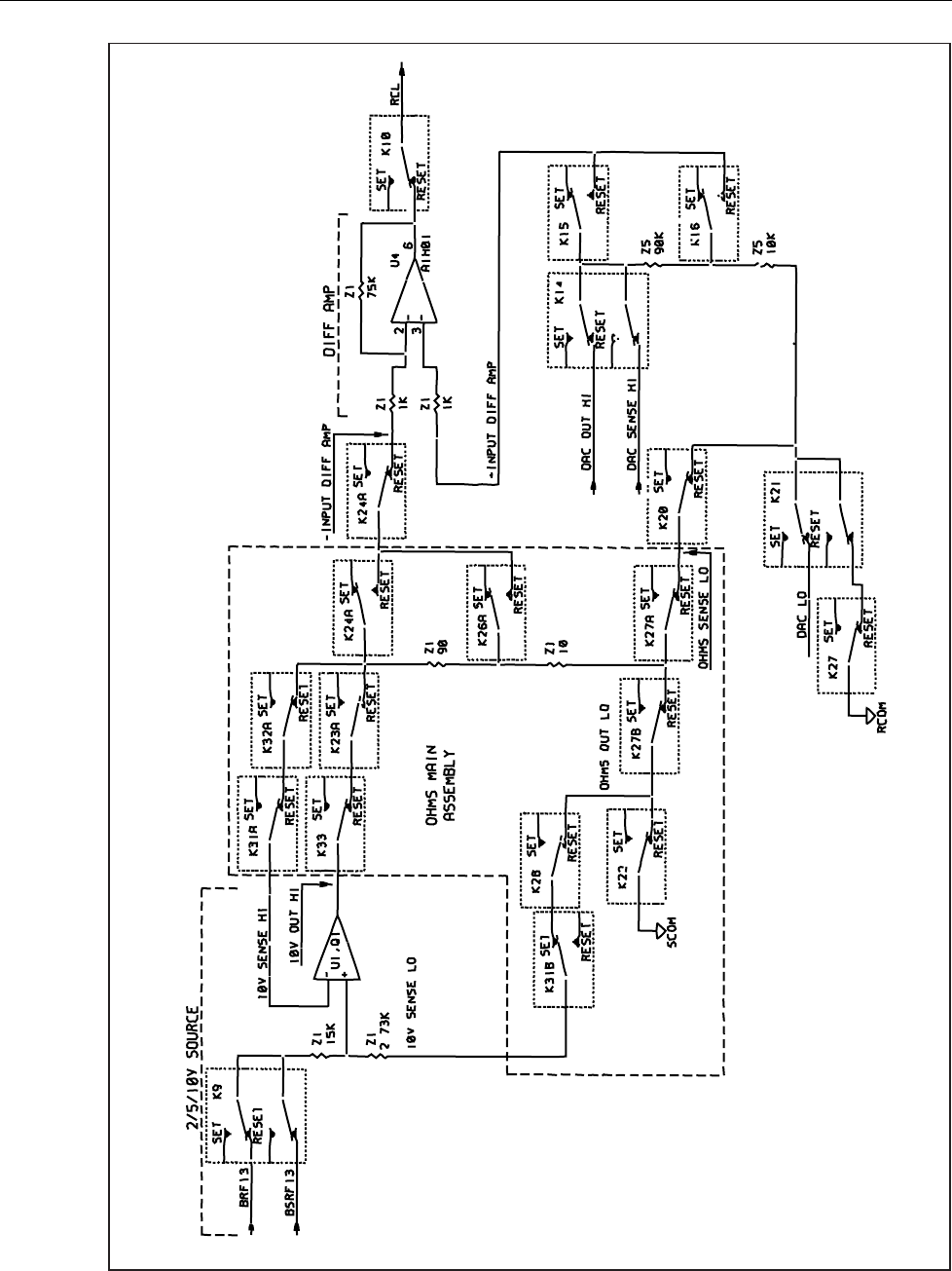
5700A/5720A Series II Calibrator
Service Manual
2-120
ahp029f.eps
Figure 2-34. Ratio Calibration, 10Ω From 100Ω

Theory of Operation
Analog Section Detailed Circuit Description
2
2-121
2-185. Calibrating to the External 1W Standard
The 1Ω and 1.9Ω resistor values are calibrated by comparing them against a 1Ω external
standard. The technique used is different from that used for the 10 kΩ external standard.
The Current assembly supplies a 130 mA (65 mA for 1.9Ω calibration) current through
both resistors. This current goes out the OUTPUT HI binding post to the 1Ω standard. It
comes back in through the OUTPUT LO binding post and through the internal 1Ω
resistance by K26 and K6, or 1.9Ω by K26 and K30 before going to S COM through
K22.
For the first reading, the inputs to the differential amplifier are connected across the
sense points of the 1Ω standard. Relay K1 connects the differential amplifier +input to
OHMS SENSE HI, which is connected to INT SENSE HI by K16 and K2 on the Ohms
Main assembly. INT SENSE HI is connected to the SENSE HI binding post by relays on
the motherboard. Relay K13 connects the differential amplifier -input to INT SENSE LO
which is connected to SENSE LO binding post by relays on the Switch Matrix assembly.
The voltage between the inputs is 0.13V, which is amplified by 75 by the differential
amplifier to approximately 9.75V and sent to the DAC assembly on the RCL line.
Another differential amplifier on the DAC assembly compares the 9.75V to the DAC
output. Before the reading is taken, however, amplifier offsets are determined.
When the DAC output equals the output of the differential amplifier on the Ohms Cal
assembly, the reading is stored and a second reading is taken. For this reading, the inputs
to the differential amplifier on the Ohms Cal assembly are connected across the 1Ω or
1.9Ω on the Ohms Cal assembly. The +input of the differential amplifier is connect
through K1 and K4 and the -input is connected through K2 and FET Q4. The second
reading is taken the same way as the first. The ratio of the two DAC settings are equal to
the ratio of the values of the two resistors. The value of the 1Ω and 1.9 ohm resistors are
determined from this ratio and the value of the external standard.
2-186. Current/High Resolution Oscillator Assembly Overview (A7)
The Current/Hi-Res (High-Resolution Oscillator) Assembly combines two functions on
one circuit board. The Current section generates dc and ac currents in the range of 20 µA
to 220 mA. The Hi-Res section generates a high-resolution signal accurate in frequency
to 4 1/2 digits, which is used by the phase-locked loop circuit on the Oscillator Output
assembly (A13). These two functions are independent circuits except for the sharing of
some digital controlling and self-diagnostic monitoring. The following theory describes
the digital control circuitry used by both circuits, then independently covers the Current
and Hi-Res functions.
The heart of the Current/Hi-Res assembly digital control circuitry is a 82C55
Programmable Peripheral Interface IC (U7), which is under software control via the
guarded digital bus. This IC has three ports which generate 24 outputs. These outputs
control three UCN5801 latching relay drivers ICs (U8-U10), a UCN5800 relay driver
(U11) for controlling non-latching relays, a 4051 analog multiplexer (U12) for self
diagnostics, and several FET switches throughout the assembly. Port A (PA0-PA7) is a
common input bus called CONTROL BUS on the schematic. This CONTROL BUS
transmits the desired state of all the relays (K1-K17) in the Current section, and also to
control two synthesizer ICs (U16, U17) in the Hi-Res section.
Four relay driver ICs drive latching controlling relays K1-K13 and K16. The CONTROL
BUS (port A of U7) is a common input bus. Port C of U7 (PC0-PC5) provides the strobe
and enable lines for these relay drivers. PC0 enables U8, while PC1 enables U9 and U10.
PC2, PC3, PC4, and PC5 strobe U11, U8, U9, and U10 respectively.

5700A/5720A Series II Calibrator
Service Manual
2-122
Relay driver U11 controls the three non-latching relays K14, K15, and K17 on this
assembly. It also generates control line RLY11* to control K11 on the Motherboard.
Relay K11 routes I-GUARD, described later, to the rear panel for operation when the
rear-panel binding posts are in use.
The diagnostic circuit allows the calibrator to monitor five points on the assembly.
Points DUMMY LOAD, OVEN TEMP, and CUR/COMP MONITOR are from the
Current section. Points HI-RES LOOP and HI-RES CLOCK come from the Hi-Res
section. Outputs PB0-PB2 select which point the multiplexer U12 monitors. PC6 enables
the output of U12 to the SDL line, where it is measured by the adc circuit on the DAC
assembly (A11).
Outputs PB3-PB5 generate control lines FET3, FET1, and FET2 respectively, which are
used by the Current section. FET1 controls NMOSFETs Q21 and Q22, FET2 controls
Q20 and Q23, and FET3 controls quad CMOS analog switches U5A, U5C, and U5D.
Output PB7 generates control line FET4, which controls analog switch U5B.
Outputs PB6 and PC7 generate control lines HI-RES RANGE and HI-RES ON/OFF
respectively, which are used by the Hi-Res section. These lines control quad CMOS
analog switch U18 and comparator U13.
2-187. Current Section
The current section of the A7 assembly uses dc voltage from the DAC assembly and ac
voltage from the Oscillator Output assembly to generate both ac and dc current outputs.
Four ranges of output current each for ac and dc are generated as shown in Table 2-14.
AC current is available from 40 Hz to 10 kHz.
Table 2-14. AC and DC Current Ranges
Range DC Current Limits AC Current Limits
220 µA 0 to 219.9999 µA 9.000 µA to 219.999 µA
2.2 mA 0.220000 mA to 2.199999 mA 0.22000 mA to 2.19999 mA
22 mA 2.20000 mA to 21.99999 mA 2.2000 mA to 21.9999 mA
220 mA 22.0000 mA to 219.9999 mA 22.000 mA to 219.999 mA
The 2.2A range is generated on the High Voltage/High Current assembly (A15) and
routed to this assembly for switching to the OUTPUT binding posts. This is further
described under the heading, "2.2A Range."
The transconductance amplifier, shunt resistors, feedback loop, and complementary
drive circuits form a loop to create the output current. In addition to these circuits, the
Current assembly contains input switching, output switching, a current guard, and a
current/compliance voltage monitor. Each of these circuits is described in detail. To
better understand the theory of operation, refer to Figure 2-35 and the schematic.
2-188. Current Input Switching
Relay K1, CMOS analog switch U5B, and FETs Q20-Q23 select the input source
voltage. For dc operation, the 22V range of the DAC assembly (A11) is brought in on the
B IN and B FB lines from the Switch Matrix assembly (A8). For ac operation, the 22V
range of the Oscillator Output assembly (A13) is brought in on the B IN and B FB lines.
During calibration of the current functions, the 13V buffered dc reference BRF13 and
BSRF13 are selected when K1 is set and U5B is closed.
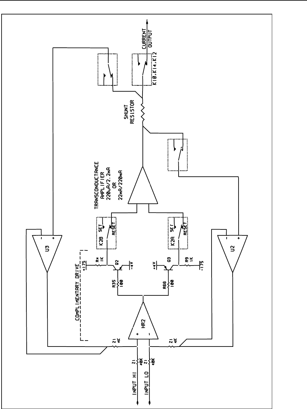
Theory of Operation
Analog Section Detailed Circuit Description
2
2-123
ahp030f.eps
Figure 2-35. Current Output Simplified Schematic

5700A/5720A Series II Calibrator
Service Manual
2-124
The input signal return paths are selected for ac or dc operation by control lines FET1
and FET2, and NMOSFETs Q20-Q23. With a dc or 13V reference input, control line
FET1 goes high, turning on Q21 and Q22, connecting RCOM and DAC OUT LO to the
respective circuit. For ac current input, control line FET2 goes high, turning on Q20 and
Q23, connecting OSC SENSE LO and OSCOM to the respective circuit.
2-189. Complementary Drive Circuit
The circuitry containing transistors Q2, Q3, Q18 and Q19 provides the complementary
drive to the output transconductance amplifiers from the single-ended output dc
amplifier on hybrid HR2. Transistors Q2 and Q18 provide the drive during a positive
input, while Q3 and Q19 provide the drive during a negative input. Relay K2 switches
the drive to the 220 µA/2.2 mA transconductance amplifiers when reset, or to the 22
mA/220 mA transconductance amplifier when set.
The HR2 assembly consists of an op amp mounted on a heated-substrate hybrid, bonded
to the shunt resistor network. The HR2 assembly gives this circuit excellent dc
characteristics of low offset, noise and drift. The hybrid heater control circuit, outlined
on sheet 2 of the schematic, adjusts the base voltage of Q1 to deliver the proper power to
the heater resistor. This maintains the HR2 assembly at a constant temperature in spite of
environmental temperature variations. Transistor Q14 protects the hybrid in case Q1
fails.
2-190. Transconductance Amplifiers
The transconductance amplifiers are the 220 µA/2.2 mA range amplifier the 22 mA/220
mA range amplifier circuits. The 220 µA and 2.2 mA ranges are provided by the 220
µA/2.2 mA range transconductance amplifier, containing transistors Q4, Q5, and relay
K3. With relay K3 reset as shown on schematic, the amplifier is in the 220 µA range. To
place the amplifier in the 2.2 mA range, relay K3 is set so emitter resistors R10 and R12
are shunted by R11 and R13 respectively.
The 22 mA/220 mA range transconductance amplifier contains transistors Q6-Q13 and
relay K4. It provides the 22 mA and 220 mA ranges. In the 22 mA range, the
transconductance amplifier is composed of Q6-Q9 with K4 in the reset position. In the
220 mA range, the transconductance amplifier is composed of Q6-Q13 with K4 in the set
position. In this range, Q10-Q13 are in the Darlington configuration with Q6-Q9
respectively. This provides the additional current gain needed for the 220 mA range.
2-191. Shunt Resistors
A resistor network is used to sense the output current in each of the four current ranges.
This network is composed of four four-terminal resistors attached to the heated substrate
of HR2. The shunt resistors are 10 kΩ for the 220 µA range, 1 kΩ for the 2.2 mA range,
100Ω for the 22 mA range, and the 10Ω for the 220 mA range. Relays K5-K9 select the
INPUT, OUTPUT, and SENSE binding posts for each of the four ranges as Table 2-15
shows.
Theory of Operation
Analog Section Detailed Circuit Description
2
2-125
Table 2-15. Relay Settings for Current Range Selection
Relay Range
220 µA 2.2 mA 22 mA 220 mA
K5 R S S S
K6 RSRR
K7 RSRR
K8 RRSR
K9 R R R S
S=SET R=RESET
2-192. Feedback Loop
The output current develops a 2.2V full-scale voltage across the appropriate shunt
resistors. Buffer amplifiers U2 and U3 isolate the shunt from the remaining feedback
circuit. The negative feedback buffer is op amp U2 configured as a voltage follower. The
positive feedback buffer is made of U3 configured as a voltage follower.
Both the feedback voltage from U2 and U3, and the input voltage from K1 and Q20-Q23
are applied to the precision dual 10:1 matched voltage divider network Z1. Any voltage
difference between the two halves of the network is amplified by the dc amplifier on the
heated substrate hybrid HR2. This amplified dc is applied to the complementary drive
circuit and in turn to the transconductance amplifiers to complete the feedback loop.
Therefore, with a 22V full scale input and the 10:1 divider, the voltage across the shunt
network is forced to 2.2V by the feedback loop. The 2.2V across the shunt is developed
by the full-scale output current on any of the four ranges. By programming the input
voltage over a 10:1 range, the output current follows with a 10:1 range. By switching the
shunt resistors, four 10:1 ranges give a total output range of 20 µA to 220 mA.
2-193. Current Output Switching
Relays K10-K15 switch the output current for the various modes of operation required
by this assembly. When K13 is reset, it switches in a dummy load (R14) to prevent
transients during switching, and also for use during diagnostics. Non-latching relay K15
connects the return lines to the output whenever an output is called for. Non-latching
relay K14 connects the output signal to latching relay K12. Relay K12 switches the
output to the AUX CURRENT OUTPUT binding post while in the reset position, or to
the OUTPUT HI binding post while in the set position.
The four ranges of output current can be connected to the B CUR line by relay K11. B
CUR is routed to the rear-panel 5725A connector. This allows all current ranges to be
available from the binding posts on the 5725A Amplifier if so selected by the operator.
2-194. Generation of the 2.2A Range
To generate the 2.2A range, the Current assembly is set to the 22 mA range with its
output directed to the High Voltage/High Current assembly (A15). This connection is
made via the IHV line by relay K10 in the set position. The High Voltage/High Current
assembly amplifies current by 100 to create the 2.2A range. This high current output is
returned to the Current assembly via the B CUR line. Relay K11 in the set position
directs it to the output relays, K12-K15, of the Current assembly.
During internal calibration of the 2.2A range, the Current assembly is set to the 22 mA
or 2.2 mA range and directed to the High Voltage assembly in the same manner as
previously described.

5700A/5720A Series II Calibrator
Service Manual
2-126
Internal calibration of the 2.2A range and gain of the High Voltage/High Current
assembly is discussed further in the theory for the High Voltage assemblies.
2-195. Current Guard Buffer
Buffer amplifier U4, configured as a voltage follower, is used to provide a guard voltage
equal to the output voltage across the external load. The guard voltage, if used, prevents
any output current from being shunted away from the load due to leakage or shunt
capacitance in the system cabling.
2-196. Compliance Limiter
A compliance limiter circuit consisting of Q24, Q25, and associated components clamps
the output to ±11V during an over-compliance condition.
2-197. Current/Compliance Voltage Monitor
The current/compliance voltage monitor circuit, which contains CMOS analog switch
U5A, U5C, U5D, op amp U6, and associated components, measures the voltage on either
side of the current shunts. This allows the Calibrator to detect an over-current or over-
compliance condition. A logic low on control line FET3 closes U5A to connect the
monitor circuit to the input side of the shunt resistor. The measurement at this point is
the sum of the output compliance voltage and voltage drop across the shunt, which is
proportional to the output current. A logic high on control line FET3 opens U5C, which
allows pull-down resistor R36 to close U5D. This connects the monitor circuit to the
output side of the shunt resistor, which gives the output compliance voltage.
Op amp U6 and associated components create an absolute value circuit whose output,
CUR/COMP MONITOR, is always a positive dc voltage. During operation in the ac
current function U6B generates a negative half-wave signal equal to the positive peaks of
its input. Resistors R31 and R30 sum this half-wave signal and the input signal at the
input of U6A. Capacitor C14 averages the voltage so the output of U6A is a dc voltage
which represents the average value of the selected input.
The diagnostic circuit connects CUR/COMP/ MONITOR to the SDL line, on which it is
routed to the DAC assembly (A11) to be measured by the adc circuit. The calibrator
software computes the difference between the two measurements and divides the result
by the shunt value to determine the output current.
2-198. Current Assembly Calibration
Refer to Figure 2-36 for the following discussion. Internal calibration of the Current
assembly is a process of determining the offset and gain constants for each of the four
current ranges.
To determine the offset of the 220 mA range, the Current assembly is set to the positive
dc 220 mA range with its input from the DAC assembly set to 0V. The output of the
Current assembly is routed to the Ohms Main assembly (A10), via INT OUT HI, where
it is connected to the previously calibrated 100Ω resistor.
To get a checkpoint reading, the Current assembly output is removed from the 100/Q
resistor on Ohms (via the output switching relays). The 100Ω resistor is connected to a
differential amplifier on the Ohms Cal assembly (A9). The output of this differential
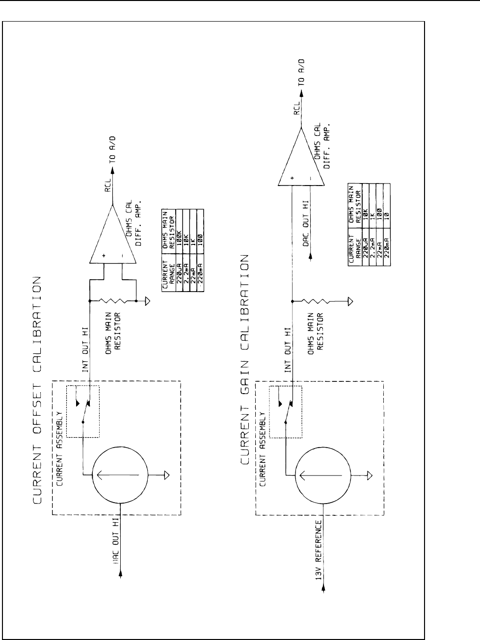
Theory of Operation
Analog Section Detailed Circuit Description
2
2-127
ahp031f.eps
Figure 2-36. Current Assembly Calibration

5700A/5720A Series II Calibrator
Service Manual
2-128
amplifier is connected to RCL, which is routed to the adc circuit on the DAC assembly.
The adc circuit measures the voltage, which is the drop across the 100Ω resistor with no
current applied through it. This value is the checkpoint reading and is stored in memory.
The output of the Current assembly is reconnected to the 100Ω resistor. Next, the DAC
assembly, which is the Current input, is adjusted until the adc circuit measures the same
reading as the check point.
Gain is determined by connecting the input of the Current assembly to the 13V reference
BRF13 and BSRF13 via relay K1 and analog switch U5B. The resulting 130 mA from
the Current assembly is routed via INT OUT HI to a previously calibrated 10W resistor
on the Ohms Main assembly. The +input of the differential amplifier, located on the
Ohms Cal assembly, is connected to one side of this 10W resistor and the -input of the
differential amplifier is connected to the output of the DAC assembly. The output of the
differential amplifier is connected to the adc circuit in the DAC assembly via the RCL
line, and the DAC output is adjusted until a null is achieved. This determines the exact
voltage drop across the 10W resistor. The exact gain can now be calculated using this
and the previous offset reading.
The current output, now calibrated at dc, is further characterized for its frequency
response. The Current assembly is configured to the ac current function with input from
the Oscillator Output assembly (A13) set to 20V at a low frequency. The output side of
the appropriate shunt resistor is connected to SCOM by relay K17B, and the resulting 2V
on the input side of the shunt resistor is connected to the AC CAL line through U22 by
relay K17A. The AC CAL signal is routed to the Oscillator Control assembly (A12)
where a 400Ω rms sensor measures the ac voltage on this line. A dc reading of the sensor
is taken. It and the Oscillator Output level are stored in memory. The Oscillator Output
frequency is then increased and the Oscillator Output level is adjusted, and stored in
memory, so the dc reading from the rms sensor is the same as the previous reading. This
is repeated at various frequencies up to 10 kHz to characterize the entire frequency
response of the ac current output.
2-199. High-Resolution Oscillator Section
The High-Resolution Oscillator supplies a square-wave signal (HI-RES) in the range of
10 Hz to 1.2 MHz with a frequency resolution of 4 1/2 digits. The output signal is routed
on the motherboard P LOCK HI line to the Oscillator Output assembly, where it phase-
locks the oscillator.
During calibrator operation using an external phase-lock signal, or during a non-ac
operation, the Hi-Res Oscillator is shut off by control line HI RES ON/OFF from the
digital control circuit. The hi-res circuitry uses a phase-locked loop circuit containing the
reference frequency amplifier/divider, phase detector/divider, loop filter, and vco circuit
as outlined on the schematic. A 5-500k divider and output switching circuitry creates the
final output frequency. These circuits are described in the following paragraphs.
The Hi-Res Oscillator output is divided into five ranges as shown below:
• 10.00 Hz to 119.99 Hz
• 0.1200 kHz to 1.1999 kHz
• 1.200 kHz to 11.999 kHz
• 12.00 kHz to 119.99 kHz
• 0.1200 MHz to 1.1999 MHz
Note that the frequency resolution on each range changes from four digits for outputs of
12 to 99 to five digits for outputs of 100 to 119. For example, the output of range 1 has
four digits of resolution from 10.00 Hz to 99.99 Hz and five digits resolution from
100.00 Hz to 119.99 Hz. The range 2 output has four digits resolution from 120 Hz to

Theory of Operation
Analog Section Detailed Circuit Description
2
2-129
990 Hz and five digits resolution from 1000.0 Hz to 1.1999 kHz. The resolution break
points are similar for the other ranges.
2-200. Reference Frequency Amp/Divider
A 2-MHz reference frequency is generated by the reference frequency amp/divider
circuit as outlined on the schematic. This circuit uses the 8 MHz system clock lines CLK
and CLK*, generated by the Guard Crossing assembly (A17). This 8 MHz signal is a
low-level clock (200 mV p-p) and it is amplified to 5V p-p by comparator U13A. This
5V 8 MHz clock is turned off when the Hi-Res Oscillator is not being used by control
line HI-RES ON/OFF from the digital control circuit and nor gate U15D. The 8 MHz
clock is then divided to 2 MHz by flip-flops U14A and U14B to generate 2 MHz REF,
which is the reference frequency for synthesizer IC U16. It is filtered by R63 and C49 to
generate HI-RES CLOCK, which is monitored by the diagnostic circuit.
2-201. Phase-Locked Loop
The phase-locked loop circuit contains the phase detector/dividers, loop filter, and vco
(voltage-controlled oscillator) circuits as outlined on the schematic.
The phase det/dividers circuit contains synthesizer IC U16. This IC contains two
programmable divide-by-n counters and a phase detector. The divide-by-n counters are
controlled by inputs from the control bus, which are latched into internal latches on the
IC. Information on the control bus is entered and latched into U16 by NOR gate U15A
and control lines CS7* and WR*. The first divide-by-n counter is programmed to divide
2 MHz REF by 2000 to give 1 kHz, which is applied to one input of the internal phase
detector. The other divide-by-n counter is used to divide the feedback frequency at pin 3,
which is generated by the VCO circuit, by 6,010 to 12,000 in one-digit steps, and then
apply it to the second input of the phase detector. The loop is locked when the two inputs
to the phase detector are the same frequency and phase.
With the 1-kHz reference frequency and the feedback divider programmed between
6,010 and 12,000, the input frequency at pin 3 of U16 must be between 6.010 MHz and
12.000 MHz (1 kHz x 6010 = 6.010 MHz and 1 kHz x 12000 = 12.000 MHz).
Phase detector (U16) outputs ("0V" on pin 14 and "0R" on pin 15) are used by the loop
filter circuit, which controls the VCO circuit. If the divided feedback frequency is
greater than the 1 kHz reference frequency, or if the phase of the divided feedback
frequency is leading the output, 0V pulses low and output 0R remains high. If the
divided feedback frequency is less than the 1 kHz reference frequency, or if the phase of
the divided feedback frequency is lagging the output, then 0R pulses low and output 0V
remains high. When the feedback frequency and the 1 kHz frequency are the same and in
phase, the outputs 0V and 0R both remain high except for a short period when both pulse
low in phase. This condition occurs when the loop is locked.
Outputs from the phase detector (0V and 0R) are connected to the loop filter circuit
which contains the two op amps in U20. U20A and U20B amplify and filter,
respectively, any phase difference and apply it to varactor diode CR9 in the vco circuit.
The vco circuit contains varactor diode CR9 and vco IC U19. The vco frequency is
controlled by CR9, which gets its bias voltage from amplifier U20. This circuit is
designed to always operate over a 2:1 range from 6 MHz-12 MHz. To lock the loop,
amplifier U20 changes the bias on varactor diode CR9 until the divided vco frequency
has the same frequency and phase as the 1 kHz reference frequency at the input to the
phase detector in U16. Once the loop is locked, the output of the phase-locked loop
circuit is between 6 and 12 MHz. This output frequency is connected to the 5-500k
divider circuit for further division.

5700A/5720A Series II Calibrator
Service Manual
2-130
Supply voltage is applied to vco U19 whenever the Hi-Res function is used by the
circuitry containing analog CMOS switch U18A, transistor Q15, and zener diode VR3.
VCO U19 is energized when control line HI-RES ON/OFF goes low to close U18A,
which turns on transistor Q15, connecting zener diode VR3 to the -17LH power supply.
R53 and R54 divide the bias voltage input of the vco circuit to generate the HI-RES
LOOP line, which is monitored by the diagnostic circuit.
2-202. 5-500k Output Divider
The 5-500k output divider circuit contains a synthesizer IC U17 which has a reference ®
divider and a divide-by-N counter. These dividers are controlled by inputs from the
CONTROL BUS, which are latched into internal latches on the IC. Information on the
CONTROL BUS is entered and latched into U17 by NOR gate U15B and control lines
CS13* and WR*. With the phase-locked loop output frequency locked at any frequency
between 6 MHz and 12 MHz, divider U17 is programmed to divide by a value between 5
and 500,000 as required to produce the correct output frequency. The 6 MHz - 12 MHz
input from the phase-locked loop circuit is divided by the reference divider to generate
the 24 kHz-2.4 MHz frequency range at pin 18. This divided reference frequency is
connected to pin 3, which is the input of the divide-by-N-counter. The divide-by-N
counter further divides the signal to generate the 20 Hz-24 kHz frequency range at pin
15.
As an example, an output of 6.7 kHz is in range 3 with the loop locked at 6.7 MHz. (The
internal divider in U16 is programmed to divide by 6,700, resulting in 6.700 MHz.) The
two dividers in U17 are programmed for a total division of 500 (6.7 MHz/500 = 13.4
kHz). This 13.4 kHz signal is divided in half by the output switching circuit to generate
the 6.7 kHz output.
2-203. Hi-Res Output Switching
The output switching circuit contains three analog CMOS switches in U18, and flip-flops
in U21. Flip-flop U21A divides the reference divider output of U17 by two to create the
12 kHz-1.2 MHz range. Flop-flop U21B divides the divide-by-N counter output of U17
by two to create the 10 Hz-12 kHz range. Control line HI-RES RANGE and NOR gate
U15C control the analog CMOS switches U18B and U18C. These switches select the 12
kHz-1.2 MHz or the 10 Hz-12 kHz frequency range, respectively, from the flip-flops.
Control line HI-RES ON/OFF and switch U18D connect this output square-wave signal
to the P LOCK HI line when the variable phase output function is activated by the
operator.
Table 2-16 shows how the dividers are set, the total division of the vco frequency, and
the vco frequency. To determine the exact vco frequency, multiply the calibrator output
frequency by the number in the total division bracket. For example, the output frequency
is set to 42 kHz and the vco frequency is 42 kHz x 200 = 8.4 MHz. Note that the total
division includes division by two by U21 in the output switching circuit.
2-204. Rear Panel Assembly (A21)
Functional circuitry on the Rear Panel assembly includes a relay control circuit, phase
lock in/variable phase out I/O circuit, address mapping, clock regeneration circuit, IEEE-
488 interface, RS-232-C interface, interfaces for the 5205A, 5215A, and 5220A
amplifiers, and a 5725A Amplifier interface. Three amplifiers can be physically
connected to the Calibrator: 5725A, 5220A with 5205A, or 5220A with 5215A. Only one
can be used at a time. Depending on the amplifier's mode of operation, the output of the
Calibrator is either an ac or a dc voltage. The following theory of operation describes
each of these circuits.

Theory of Operation
Analog Section Detailed Circuit Description
2
2-131
2-205. Rear Panel Power Supplies
Power supplies are divided into guarded and unguarded. Unguarded supplies +5V
LOGIC, +12V, and -12V are referenced to +5V LOGIC COMMON and are generated on
the Digital Power Supply assembly (A19). Guarded supplies +5LH and -5LH are
referenced to LH COM, and the supply +5RLH is referenced to RLH COM. These
supplies are generated on the Regulator/Guard Crossing assembly (A17). Some ICs on
the A17 assembly do not have power and ground pins shown on the schematic. This
information is included in the table on sheet 1 of the Rear Panel schematic.
Table 2-16. Divider Settings and VCO Frequencies
Calibrator Output
Frequency at
TP16
U17 R Divider
Setting
U17 N Divider
Setting
Total Division
of VCO at
TP13
VCO Frequency
at TP13
10 Hz to 12 Hz 500 1000 1M 10 MHz to 12 MHz
13 Hz to 15 Hz 400 1000 800k 10.4 MHz to 12 MHz
16 Hz to 30 Hz 200 1000 400k 6.4 MHz to 12 MHz
31 Hz to 60 Hz 100 1000 200k 6.2 MHz to 12 MHz
61 Hz to 120 Hz 50 1000 100k 6.1 MHz to 12 MHz
130 Hz to 150 Hz 400 100 80k 10.4 MHz to 12 MHz
160 Hz to 300 Hz 200 100 40k 6.4 MHz to 12 MHz
310 Hz to 600 Hz 100 100 20k 6.2 MHz to 12 MHz
610 Hz to 1.2 kHz 50 100 10k 6.1 MHz to 12 MHz
1.3 kHz to 1.5 kHz 400 10 8k 10.4 MHz to 12 MHz
1.6 kHz to 3.0 kHz 200 10 4k 6.4 MHz to 12 MHz
3.1 kHz to 6.0 kHz 100 10 2k 6.2 MHz to 12 MHz
6.1 kHz to 12 kHz 50 10 1k 6.1 MHz to 12 MHz
13 kHz to 15 kHz 400 0 800 10.4 MHz to 12 MHz
16 kHz to 30 kHz 200 0 400 6.4 MHz to 12 MHz
31 kHz to 60 kHz 100 0 200 6.2 MHz to 12 MHz
61 kHz to 120 kHz 50 0 100 6.1 MHz to 12 MHz
130 kHz to 150
kHz
40 0 80 10.4 MHz to 12 MHz
160 kHz to 300
kHz
20 0 40 6.4 MHz to 12 MHz
310 kHz to 600
kHz
10 0 20 6.2 MHz to 12 MHz
610 kHz to 1.2
MHz
5 0 10 6.1 MHz to 12 MHz
2-206. Rear Panel Address Mapping
The rear panel decodes address lines from the bus connected to the main CPU through
connector P91. Decoding is accomplished with a C22V10 PLD (U8) with the following
chip selects:
• RPDUARTCS*, D00000-D0001F
• RPIEEECS*, D00020-D0002F
• Y52XXRD*, D00030-D00031
• Y5205WR*, D00032-D00033
• Y5220WR*, D00034-D00035

5700A/5720A Series II Calibrator
Service Manual
2-132
2-207. Clock Regeneration Circuit
In order to minimize EMI (electro-magnetic interference) inside the Calibrator chassis,
the rear panel accepts a low-level (~200 mV p-p sinewave) 3.68 MHz clock from the
CPU assembly and conditions it to proper TTL clock levels.
This is done by a differential amplifier, U18, which amplifies the incoming signals
3.6864MHZCLK and 3.6864MHZCLK*. The output of U18 is a TTL level 3.68 MHz
clock called RP3.68MHZ that is buffered by PLD U8 creating RPCLK for use by
DUART (dual universal asynchronous receiver/transmitter) U5, and IEEE interface IC
U2.
2-208. IEEE-488 (GPIB) Interface
The IEEE-488 (GPIB) interface circuit provides the interface between the IEEE-488
connector (J1) and the calibrator processor on the CPU (A20) assembly. The circuitry
uses a TMS9914 (U2) General Purpose Interface Bus (GPIB) adapter to meet the
requirements for talker/listener operation on the IEEE-488 bus. This circuit translates
asynchronous 8 bit data and control information, under control of an external controller,
and converts this information to an acceptable format for the CPU. responds.
The TMS9914 has internal circuitry which handshakes in the proper GPIB protocol and
stores data in an internal buffer. This IC also has the capability of interrupting the CPU.
The CPU can then handle the interrupt through its own handler routine. The data lines
between U2 and J1 are buffered by a 75160A (U3) data buffer, and the command lines
are buffered by a 75162A (U4) command buffer. J1 is a standard IEEE-488 connector.
The shell of this connector is tied to chassis ground for EMI/RFI shielding.
2-209. RS-232C Interface
The RS-232C interface circuit uses a 68C681 DUART (U5), a 1488 line driver (U6), and
a 1489 line receiver (U7).
The DUART does the parallel to serial data conversion and provides two channels of
serial RS-232C communication.
The first channel is available to RS-232C connector J2 to meet serial interface needs
between the Calibrator and the external world. The transmit line (*TXDA) is driven by
U6D to TX of J2, pin 2. The receive line RX goes from J2, pin 3 through receiver U7C
to the receive line *RXDA of the DUART.
The second channel is connected to the 5725A Amplifier interconnect connector (J7) to
provide the 5725A digital control interface to the CPU assembly. Transmit line *TXDB
is driven by U6B to B-SCT of J7, pin 18. Receive line B-SCR from J7, pin 17 goes
through receiver U7B to the receive line *RCVB of the DUART. These lines are also
connected to J10, pins 2 and 3, for internal software testing.
The DUART (U5) also has six input lines, four of which are used to monitor CTSA*, B-
CINT*, CAL SWA*, and CAL SWB*. The CTS (clear to send) line from J2, pin 5 goes
through receiver U7A becoming CTSA*. Line CAL SWA* comes from the rear panel
CALIBRATION switch.
The B-CINT* input (5725A cable interlock) is a logic signal used to let the Calibrator
know that the interface cable to the 5725A Amplifier is connected and the 5725A is
energized.
The DUART (U5) generates four output lines. The first, RTSA*, is driven by U6C to the
RTS (ready to send) pin 4 of J2. The remaining three are used in the auxiliary amplifier
interface logic circuit.

Theory of Operation
Analog Section Detailed Circuit Description
2
2-133
5220EN* is the output enable for octal latch U10. 5220ADIR* is the output enable for
buffer U11. 5205EN* is the output enable for octal latch U9.
2-210. Auxiliary Amplifier Interface
A 5725A amplifier can be physically connected to the 5700A/5720A Series II. Only one
can be used at a time. Depending on the amplifier’s mode of operation, the output of the
Calibrator is either an ac or a dc voltage.
2-211. 5725A Interface
The Calibrator is designed to work in close connection with the 5725A Amplifier. The
rear panel in this system provides relay switching for the 5725A signals. All voltage
outputs from the 5725A are routed back to the binding posts on the Calibrator. All
current outputs from the 5725A are sourced at the 5725A OUTPUT binding posts. You
can configure the Calibrator to also source all its current outputs through the 5725A
OUTPUT binding posts for convenience.
Connector J8 and Cable 4406 interface all the Calibrator I/O signals between the
Motherboard and the rear panel. Connector J7 interfaces the Calibrator to the 5725A
Amplifier. The interface between these two connectors is accomplished through relays
K1, K2, and K6-K9. Relays K6-K9 break all the I/O lines except B-SENSE HI, B-OUT
HI, V-GUARD, and B-IGRD, and connect them all to V-GUARD when the 5725A is not
in use.
During 5725A operation, relays K1, K2, K6, and K7 switch the Calibrator analog signals
B IN, B FB, B SNSLO, and PACOM to lines BOOST IN, B-FEEDBACK, B-SENSE
LO, and BPA COM on connector J7.
High voltage output of the 5725A (B-OUT HI and B-SENSE HI) is connected to the
Calibrator Motherboard via cable 4406 where it can be switched to the Calibrator
binding posts by relays on the motherboard.
Relays K8 and K9 connect the 5725A current function lines I-RET, and B-CUR on
connector J8 to B-IRTN, and B-CURRENT, on connector J7 when the 5725A is
outputting Calibrator current (≤2.2A). Line B-RCL is used during 5725A calibration.
Line B-RCL on J7 is connected to J8 through relay K6. Line B-RCL is routed via the
motherboard to the Current assembly (A7) where it is switched to the calibrator RCL
line by a relay.
2-212. Phase Lock In/Variable Phase out
The Oscillator Output assembly (A13) can be phase locked to an external signal
connected to the PHASE LOCK IN BNC connector J6. Relay K10B connects the shell of
this BNC connector to chassis ground through protection resistor R19 when the
Calibrator is on internal operation, or to P LOCK LO when the Calibrator is phase
locked to the external signal coming in on J6.
This incoming signal is called PHLK IN on the schematic. Relay K10A switches an
external phase-lock signal from J6 to the input of Q1 and Q2. FETs Q1 and Q2 provide
current limiting for PHLK IN. Signal P LOCK is routed to connector J8 where it is
connected to the Oscillator Output assembly via the Motherboard.
Components CR1, CR2, VR1, VR2, R4, and R5 provide amplitude protection for the
phase lock circuitry on the Oscillator Output assembly by limiting the amplitude of P
LOCK.
The Variable Phase Out BNC connector (J5) is connected to P SHIFT and its shell is
connected to PA COM by energizing relay K12. Signal P SHIFT is a fixed-amplitude
variable phase signal generated by the Oscillator Output assembly (A13). Refer to the

5700A/5720A Series II Calibrator
Service Manual
2-134
Oscillator Output assembly theory of operation for a detailed description on the
generation of P SHIFT. Resistor R18 serves as overcurrent protection for the BNC shell
connection on J5.
2-213. Rear Panel Relay Control
The relays on the Rear Panel assembly are used as the interfaces for the 5725A
amplifier, or for switching the PHASE LOCK IN and VARIABLE PHASE OUT signals.
The relay switching circuitry is under control of the guarded digital bus via connector J8.
This guarded digital bus is generated on the Regulator/Guard Crossing assembly (A17).
The relay control circuitry is located on sheet 5 of the Rear Panel schematic. This circuit
uses an 82C55 programmable peripheral interface (U14) and two relay drivers (U16 and
U17) to control the 12 relays on this assembly and one relay (K12) on the Analog
Motherboard. The 82C55 (U14), which is under control of the guarded digital bus via
connected J8, has three ports generating 24 outputs.
Port A (PA0-PA7) provides the input lines for relay driver U16.
Port B (PB0-PB7) provides the input lines for relay driver U17.
PC0-PC2 of port C provides the CLEAR, STROBE, and OUTPUTENABLE lines for
these relay drivers.
Relay Driver U16 controls two latching relays (K2 and K3) and four non- latching relays
(K1, K4, K5, and K7). Relay driver U17 controls one latching relay (K6) and five non
latching relays (K8-K12). Relay driver U17 also creates control line RLY12* (pin 13)
which controls relay K12 on the Analog Motherboard assembly (A3).
2-214. Rear Panel CPU Interface
The rear panel is interfaced to the CPU assembly (A20) via connector J8 on the rear
panel. The CPU has:
• Five address lines (RPA1-RPA5) which comprise the ADDRESS BUS

Theory of Operation
Analog Section Detailed Circuit Description
2
2-135
• Seven control lines which comprise the CONTROL BUS
• A low-level 3.6864 MHz clock (CLOCK, CLOCK*)
• Eight data lines RPD0-RPD7
Interfacing between the Rear Panel data bus (D100-D107) and the CPU data bus (RPD0-
RPD7) is done with a bus transceiver U1.
2-215. Wideband AC Module (Option -03)
The Option -03 Wideband AC Module consists of the Wideband Oscillator assembly
(A6) and the Wideband Output assembly (A5).
The wideband module operates in conjunction with the Oscillator Output assembly
(A13), and provides calibrated output voltages in the range of 300 µV to 3.5V rms at
frequencies of 10 Hz to 30 MHz, into a 50Ω load resistance. The output impedance of
the assembly is 50Ω. It is designed to drive 50Ω loads. The output of this option
connects to the Type "N" wideband connector on the Calibrator front panel.
Theory of operation for the Wideband Oscillator assembly (A6) and the Wideband
Output assembly (A5) follows under separate headings.
2-216. Wideband Oscillator Assembly (A6)
The Wideband Oscillator assembly generates sine wave outputs in the range of 1.1 MHz
to 30 MHz, (with two-digit resolution) at a nominal full scale output of 700 mV rms.
The frequency source is a ECL-level square wave with a frequency range of 1.1 MHz to
30 MHz, created in the phase-locked loop and divider circuit. The amplitude of this
square wave is controlled by the WB AMPLITUDE CONTROL line, which is a DC
signal from the Wideband Output assembly, and the circuitry contained in the amplitude
control amplifier.
The resulting variable frequency and amplitude square wave is converted to sine wave
by one of the five-pole filters. This variable frequency and amplitude sine wave is routed
to the Wideband Output assembly via connector J1 and a 75Ω coaxial cable.
2-217. Wideband Oscillator Power Supplies
The +5LH, -5LH, +17S, and -17S supplies are generated on the Regulator assembly and
routed to this assembly via the motherboard.
The -5LH supply is buffered by L12 and C49, creating the -5F supply.
The +5LH supply is divided by R66 and R67 to create the +2.5 supply which is the
reference voltage for comparators in U7, U10, and U11.
Zener diode VR1 and resistor R39 create the +12 supply from the +17S supply. Zener
diodes VR4 and VR5, resistors R40 and R41, and diodes CR8 and CR9 create the -12, -
11, and -9.5 supplies from the -17S supply. These are used throughout the Wideband
Oscillator assembly.
2-218. Wideband Oscillator Digital Control
The digital control circuit on the Wideband Output assembly creates control lines WB
MUXA, WB MUXB, WB MUXC, WB FBS, and WB ON/OFF*. These lines are routed
to the Wideband Oscillator via the motherboard.
Control lines WB MUXA, WB MUXB, and WB MUXC are inverted and level-shifted
by comparators in U7 to create the control lines for multiplexer U6. They are also used
by the filter-select circuitry.

5700A/5720A Series II Calibrator
Service Manual
2-136
In this circuit, WB MUXA, WB MUXB, and WB MUXC are decoded by U8 to generate
four control lines, These are inverted and level-shifted by comparators in U10 and U11.
The output of these comparators create 16-32 MHz FILTER, 8-16 MHz FILTER, 4-8
MHz FILTER, 2-4 MHz FILTER, 1-2 MHz FILTER, and Q8/Q9 SELECT, which are
used in the filter switch drive circuitry.
Control line WB FBS is inverted and level-shifted by a comparator in U10. This creates
FILTER BAND SWITCH, which is also used in the filter selection circuitry. Control
line WB ON/OFF* shuts down the 8 MHz clock generator and vco when the wideband
module is not in use.
2-219. Phase-Locked Loop and Divider Circuit
The phase-locked loop and divider circuit uses 8 MHz clock generator U15, synthesizer
IC U1, amplifier U2, vco U3, and dividers in U4 and U5 to generate an ECL-level square
wave from 1.1 MHz to 30 MHz.
The 8 MHz clock generator creates the 8 MHz reference frequency from the 8 MHz
system clock lines CLK and CLK*, which is a low level (~200 mV p-p) 8 MHz sine
wave generated on the Regulator/Guard Crossing (A17) assembly. Comparator U15
converts this sine wave into a TTL-level 8 MHz square wave to provide the reference
frequency for synthesizer IC U1.
Synthesizer IC U1 contains two programmable divide-by-N counters and a phase
detector. The divide-by-N counters are controlled by inputs from the guarded digital bus,
which are latched into internal latches on the IC. NOR gates in U14 are used to gate the
chip select (CS14) and write (WR) lines from the digital bus. This forms the strobe pulse
necessary to latch the frequency data into the synthesizer IC.
The first divide-by-N counter is programmed to divide the 8 MHz reference by 160 to
give 50 kHz. This, in turn, is applied to one input of the internal phase detector. The
other divide-by-N counter is used to divide the feedback frequency at pin 3 by 80 to 160
in 1 digit steps, and then apply it to the second input of the phase detector. The loop is
locked when the two inputs to the phase detector are the same frequency and phase.
With a 50 kHz reference frequency and the feedback divider programmed between 80
and 160, the input frequency at pin 3 (feedback frequency) must be between 4 MHz and
8 MHz. (50 kHz x 80 = 4 MHz and 50 kHz x 160 = 8 MHz.)
The frequency into U1 pin 3 is generated by the vco (U3) and dividers in U4 and U5. A
flip flop in U4 divides the vco frequency by 2 and the binary counter in U5 further
divides by 4 to give a total division of 8.
If the input to U1 pin 3 is between 4 MHz and 8 MHz, then the vco frequency before the
divide-by-8 must be 32 MHz to 64 MHz.
The phase detector outputs ("0V" on pin 14 and "0R" on pin 15) of the synthesizer U1
are used by the amplifier (U2) to control the vco (U3). If the divider feedback frequency
is greater than the 50 kHz reference frequency, or if the phase of the divider feedback
frequency leads the output, then 0V pulses low while output 0R remains high.
If the divider feedback frequency is less than the 50 kHz reference frequency, of if the
phase of the divider feedback frequency lags the output, then 0R pulses low and the
output 0V remains high.
When the feedback frequency and the 50 kHz reference frequency are the same and in
phase, the output 0V and 0R both remain high except for a small period when both pulse
low in phase. This condition occurs when the loop is locked.

Theory of Operation
Analog Section Detailed Circuit Description
2
2-137
The vco frequency is controlled by varactor diodes, CR1 + CR2, which get their bias
voltage from amplifier U2. Amplifier U2, which gets its input from the phase detector
outputs (0V and 0R) of U1, changes the bias on varactor diodes CR1 and CR2 until the
divided vco frequency has the same frequency and phase as the 50 kHz reference
frequency at the input to the phase detector in U1.
Any phase difference is amplified by U2 and filtered by L6, C53, and C17 to bring the
loop into lock.
The vco is shut off whenever the Wideband AC module is not in use. To shut off the vco
control line WB ON/OFF* is set low and inverted by a comparator in U7 which then
turns on Q3.
With transistor Q3 on, transistor Q2 is turned off which removes the -5V supply from the
vco to stop the oscillation.
With the vco frequency between 32 and 64 MHz, U4 divides by 2 to give a symmetrical
square wave of 16 to 32 MHz, which is the top octave range required for this assembly.
Further division by two (pin 15), four (pin 13), eight (pin 4), and sixteen (pin 2) by
binary counter U5 gives the other ranges required of 8 to 16 MHz, 4 to 8 MHz, 2 to 4
MHz, and 1 to 2 MHz.
Multiplexer U6, under software control via control lines WB MUXA, WB MUXB, WB
MUXC, and comparators in U7, can be programmed to select which of the 5 ranges is
needed to give the output frequencies of 1 to 32 MHz.
2-220. Amplitude Control Amplifier and X10 Wideband Amplifier
The square wave output generated by the phase-locked loop and divider circuit (1-32
MHz OUTPUT) is connected to the amplitude control amplifier circuit.
This circuit uses transistor array U9 to form a differential gain-control amplifier. Gain of
the amplifier is controlled by the dc signal AMPLITUDE CONTROL, connected to U9
pin 10.
DC signal AMPLITUDE CONTROL is generated by the thermal rms sensor amplitude
control circuitry on the Wideband Output assembly (A5) and is discussed in that section.
The gain controlled square wave output of U9 (pin 6) is further amplified by the x10
wideband amplifier circuit. Transistors Q4, Q5, and Q6 are configured as an amplifier
with a gain of ten. This amplifier raises the gain-controlled square wave to the level
needed to drive output filters. The output of this circuit is a square wave with an
amplitude between 1.4V p-p to 6.0V p-p.
2-221. Wideband Oscillator Filters
Each of the five octave frequency ranges has a 5-pole filter to change the square wave
input to a sine wave output with a nominal full scale output of 700 mV rms.
The filter switch drive circuit uses control lines from the filter select circuit (that
contains transistor arrays U12 and U13) to provide the drive to properly turn on and off
FETs and transistors in each of the filters.
The filter inputs and outputs are switched on by FETs and the filter output is applied to
output driver Q7. The corresponding filter is selected automatically as each octave range
is selected. The operation of the 16-32 MHz filter is described. The other four filters
operate in a similar fashion.
The input FET Q101 is turned on via control line 16-32 MHz FILTER and a transistor in
U13. This applies the signal FILTER INPUT from the X10 wideband amplifier to
follower Q102. Transistor Q102 drives the filter that contains L102, L103, L104, C109

5700A/5720A Series II Calibrator
Service Manual
2-138
and C112. FET Q105 is turned on, in the same manner as FET Q101, to connect the sine
wave output of this filter to FILTER OUTPUT. This is applied to output driver transistor
Q7.
To obtain the required amount of filtering over the entire octave range, additional
capacitors C110 and C111 are switched into the filter by PIN diodes CR102 and CR103
when operating below 70% of the full range (22 MHz in this case).
Diodes CR102 and CR103 are activated by turning on Q103 and Q104, respectively.
Transistors Q103 and Q104 are turned on via control line Filter Band Switch and a
transistor in U12.
Two additional FETs, Q8 and Q9, are used to isolate the 16-32 MHz filter and the 8-16
MHz filter, from the three other lower frequency filters, whenever the two high
frequency filters are used. The isolation provided by FETs Q8 and Q9 eliminates both
the input and output load capacity and circuit board capacity of the three lower
frequency filters, so that follower Q6 can drive the high frequency filter input without
distortion of the waveform. This also eliminates loading the filter outputs, which changes
the filter frequency response.
2-222. Wideband Output Assembly (A5)
The Wideband Output assembly (A5) takes the sine wave signal from either the
Wideband Oscillator assembly (A6) or the Oscillator Output assembly (A13), and
amplifies it to a power level that drives 3.5V into a 50Ω load at the output.
The Oscillator Output assembly generates the sine wave signal from 10 Hz to 1.1 MHz,
and the Wideband Oscillator assembly generates the sine wave signal from 1.2 MHz to
30 MHz. This provides a total frequency range of 10 Hz to 30 MHz.
The Wideband Output assembly contains a power amplifier circuit that increases the
gain and/or power level of the input signal. Also contained on the assembly are a thermal
rms sensor circuit necessary for amplitude control, the 50Ω attenuators needed to reduce
the output level through all of the amplitude ranges, an overload control circuit, and
digital control circuitry.
Figure 2-37 is a simplified schematic for the Wideband Output assembly.
The Wideband Output assembly has three basic operating ranges:
1. The first range is for Wideband AC module operation at frequencies between 10 Hz
and 11.9 kHz. In this frequency range, relay K1A is in the set position so the input
signal is from the Oscillator Output assembly with its amplitude is controlled by the
Oscillator Control assembly (A12). The amplitude control circuit on the Wideband
Output assembly is only used for overload protection. This is done by control line
PB0 which goes high and turns on FETs Q2 and Q3 via comparator U4B. These
FETs shunt the rms sensor’s input and output to ground through 200Ω resistors (R2
and R18) to reduce the sensitivity of the sensor.
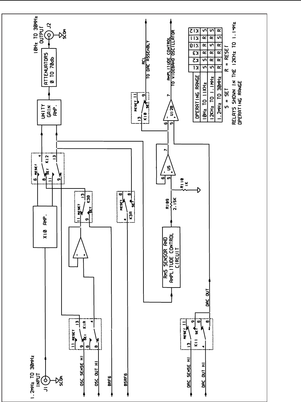
Theory of Operation
Analog Section Detailed Circuit Description
2
2-139
ahp032f.eps
Figure 2-37. Wideband Output Assembly Simplified Schematic

5700A/5720A Series II Calibrator
Service Manual
2-140
2. The second range is for operation at frequencies between 12 kHz and 1.1 MHz. In
this mode the input signal is also from the Oscillator Output assembly, but the
amplitude is controlled by the amplitude control circuit on the Wideband Output
assembly. Relay K10 is in the set position to connect the output of the rms sensor
and amplitude control circuit to the RCL line where it is measured by the adc circuit
on the DAC assembly. The DAC assembly operates in conjunction with the
Oscillator Control assembly to adjust the amplitude of the Oscillator Output signal.
3. The third range is for operation at frequencies between 1.2 MHz and 30 MHz. In this
mode the input signal is from the Wideband Oscillator assembly via connector J1. Its
amplitude is controlled by the amplitude control circuit on the Wideband Output
assembly. In this mode, the output of the DAC assembly, DAC OUT HI and DAC
SENSEHI, are connected to DAC OUT by relay K11 in the set position. Op amp
U12B compares DAC OUT to the output of the rms sensor and amplitude control
circuit. Any difference between these two signals is amplified and routed to the
Wideband Oscillator assembly via the AMPLITUDE CONTROL line. The
Wideband Oscillator uses the Amplitude Control line to adjust its AC amplitude
until the sensor output is equal to the DAC voltage.
2-223. Wideband Output Power Amplifier Circuit
The power amplifier circuit, as outlined on sheet 1 of the Wideband Output assembly
schematic, contains all the circuitry shown on sheet 2 of the schematic. This circuitry
consists of the x10 amplifier, the unity-gain amplifier, and the 10 Hz to 1.1 MHz buffer
circuit as outlined on the schematic.
The x10 amplifier circuit is used only during operation in the 1.2 MHz to 30 MHz range.
The 1.2 MHz to 30 MHz sine wave input comes from the Wideband Oscillator assembly
via a coaxial cable and connector J1. This input signal has a nominal full-scale amplitude
of 700 mV rms.
The x10 amplifier circuit uses transistors Q4, Q5, Q6, Q7, Q8, Q9, and Q10 to amplify
this signal by a factor of 10. Amplifier U11A keeps the DC offset on the output to near
zero. The output of the X10 amplifier is applied to the unity gain amplifier by relay K12
in the reset position. The output impedance of the unity gain amplifier is 50Ω, therefore
the x10 amplifier must produce 7.0V rms to give 3.5V rms into the 50Ω load.
The 10 Hz to 1.1 MHz buffer circuit is used during operation in the 10 Hz to 12 kHz
range or the 13 kHz to 1.1 MHz range. In this mode, the input signal comes from the
Oscillator Output assembly. This input signal is buffered by Q17 and applied to relay
K12. Amplifier U11B keeps the DC offset on the output near zero for the 10 Hz to 1.1
MHz range.
The unity-gain amplifier is connected to either the output of the x10 amplifier or the
output of the 10 Hz to 1.1 MHz Buffer by relay K12. The unity gain amplifier uses
transistors Q11-Q16 and associated components. This circuit increases the power to a
level that drives 3.5V rms into a 50 ohm load. The four 1/2-watt resistors in parallel
(R96, R97, R98, R99) along with the output resistance of the amplifier form the 50Ω
output resistance.
The output of this amplifier, called 10HZ TO 30MHZ OUTPUT, is a sine wave with an
amplitude between 1.1V and 3.5V rms into 50Ω. This output signal is used by the
attenuators to provide the overall output range of the Wideband Output assembly.
Resistors R41 and R42, and capacitor C23 divide this output signal to create OUTPUT
OFFSET for diagnostics.

Theory of Operation
Analog Section Detailed Circuit Description
2
2-141
2-224. Wideband Output Attenuators
The 10 Hz to 30 MHz sine wave signal output of the power amplifier circuit connects to
the 50Ω output attenuator composed of attenuator networks Z1 and Z2 and relays K4,
K5, K6, K7, and K8.
Relay K4 switches the 10 dB attenuator into the circuit when activated or bypasses it
when not activated.
Relay K5 switches the 20 dB attenuator into the circuit when activated or bypasses it
when not activated.
Relays K6 and K7 switch the 40 dB attenuator into the circuit when activated and bypass
it when not activated. The attenuator can thereby reduce the signal level in 10 dB steps
from 0 to 70 dB.
Power Amplifier output amplitude is continuously variable over a 10 dB range, which
when combined with the 0 to 70 dB attenuator, gives a continuous output range of 300
µV to 3.5V rms.
When energized, relay K8 enables the output signal to be connected to the output coaxial
connector J2.
2-225. Wideband Output RMS Sensor and Amplitude Control Circuit
The rms sensor circuit is used for:
• Amplitude control
• Overload control over the frequency range of 12 kHz to 30 MHz
• Overload control only over the frequency range of 10 Hz to 12 kHz
The rms sensor and amplitude control circuit is composed of U1, U2A, U2B, U3, U5,
U12A, U12B, and associated components. Thermal sensor U1 provides a dc voltage
equal to the rms value of the input voltage (at pin 6).
Input voltage to the thermal sensor comes from the power amplifier circuit. DC voltage
output from the thermal sensor is connected to U2A configured as an integrator. The
output of the integrator is connected to a square-root amplifier configured by U2B U3,
and U12A, which keeps the settling time of the sensor constant.
The dc output of this sensor circuit (available at TP1) is buffered by U5. In the 12 kHz to
1.1 MHz range, the output of U5 is connected to the RCL line by relay K10 in the set
position. In the 1.2 MHz to 30 MHz range, the output of U5 is compared by U12B to
DAC OUT.
The DAC assembly (A11) output, DAC OUT HI and DAC SENSE HI, are tied together
by relay K11 to create DAC OUT.
Relay K2A connects capacitor C7 into the rms sensor circuit in the 10 Hz to 11 kHz
range to add additional filtering for low frequency signals.
2-226. Wideband Output Overload Control Circuit
The overload control circuit contains comparator U4 (A and B), FETs Q2 and Q3,
transistor Q1, and associated circuitry. This circuit protects the rms sensor and
attenuators during an overload condition. Comparator U4A detects an overload condition
by comparing the dc output of the rms sensor against a reference voltage.
The reference voltage is determined by zener diode VR2 and resistor R21. If the dc
output of the rms sensor reaches a voltage 10% greater than the normal full-scale
voltage, the output of U4A goes negative. This negative voltage causes a positive voltage
at the output of U4B which turns on FETs Q2 and Q3. These FETs protect the rms

5700A/5720A Series II Calibrator
Service Manual
2-142
sensor from damage by shunting its input and output to ground through the 200Ω
resistors R2 and R18.
The negative voltage at the output of U4A also turns off transistor Q1 and causes control
line U9 ENABLE to go high. This disables relay driver U9, which turns off all attenuator
relays (K4-K7) and output relay K8.
2-227. Wideband Output Digital Control
The heart of the Wideband Output assembly digital control circuitry is a 82C55
programmable peripheral interface IC (U7), which is under software control via the
guarded digital bus.
This IC has three ports, generating 24 outputs. These outputs control three relay drivers
(U6, U9, U10) and a 4051 analog multiplexer IC (U8) for self diagnostics.
Port A (PA0-PA7) is used as a common input bus for the relay drivers. Relay driver U6
controls latching relays K1, K2, K10, K11, and K12. Driver U6 is enabled by PC3 and
strobed by PC2. Relay driver U9 controls non-latching relays K4-K8. Driver U6 is
strobed by PC0 and enabled by control line U9 ENABLE, which is generated in the
overload control circuit. Relay driver U10 controls latching relays K3 and K9. It is
strobed by PC1 and enabled by PC3.
Relays K1 and K12 are controlled by the same drive lines and, when in the set position,
select the input from the Oscillator Output (A13) assembly during operation between 10
Hz and 1 MHz.
Relay K9 connects a 50Ω load (R43 and R44 in parallel) to the RCL line where the adc
circuit on the DAC assembly can monitor the output voltage and thereby determine
proper operation of the output attenuator resistors and relays.
The 4051 analog multiplexer IC (U8) is used by self-diagnostic routines for the
Wideband AC module. This allows the Calibrator to monitor three points on the
Wideband Output assembly and one point on the Wideband Oscillator assembly. Points
AMPLITUDE CONTROL, OUTPUT OFFSET, and SENSOR CAL are monitored on the
Wideband Output assembly, and point PLL DIAGNOSTIC is monitored on the
Wideband Oscillator assembly. PC4-PC6 of port C select which point the multiplexer
monitors. PC7 enables the output of U8 to the SDL line where is measured by the adc
circuit on the DAC assembly (A11).
2-228. Wideband Output Calibration
Linearity of the rms sensor is determined by configuring the Wideband Output similarly
to the second range of operation as described earlier. A difference is that the Oscillator
Output assembly operates at 1 kHz instead of between 12 kHz and 1.1 MHz during
operating in this range.
The Oscillator Output is set to 2.5V at 1 kHz. The resulting dc voltage from the rms
sensor is connected to the RCL line by relay K10 in the set position. The RCL line is
routed to the +input of the adc circuit on the DAC assembly, and the adc -input is
connected to the DAC output. The difference between the two is measured and stored in
memory. The Oscillator Output is increased to 7.0V and the difference between the two
adc inputs is again measured. Software uses these values to determine the linearity of the
rms sensor.
The previously calibrated 6.5V reference BRF6 and its sense line BSRF6, from the DAC
assembly is used to calibrate the 10 dB, 20 dB, and 40 dB attenuators.
Relays K3 A and B and K12 are in the set position. This connects the 6.5V reference to
the unity-gain amplifier and the attenuators. Output at the WIDEBAND Type "N"

Theory of Operation
Analog Section Detailed Circuit Description
2
2-143
connector is connected back to the OUTPUT HI SENSE and OUTPUT LO SENSE
binding posts.
Attenuation is calibrated starting with 70 dB and decreased in 10 dB steps to 0 dB. The
Switch Matrix assembly connects the output of the Wideband AC module to its internal
cal zero amplifier circuit during all attenuator calibrations except the 0 dB and 10 dB.
The internal cal zero amplifier circuit provides a gain of 10 to Wideband output during
20 dB to 70 dB attenuation calibration. The output of this amplifier is connected to the
RCL line which is routed to the +input of the adc circuit on the DAC assembly. Output
from the DAC is connected to the -input of the adc circuit and adjusted until a null is
achieved. The exact attenuator value is then determined.

5700A/5720A Series II Calibrator
Service Manual
2-144
3-1
Chapter 3
Calibration and Verification
Title Page
3-1. Introduction .......................................................................................... 3-3
3-2. Accessing the Fuse............................................................................... 3-4
3-3. Cleaning the Air Filter.......................................................................... 3-5
3-4. Cleaning the Exterior ........................................................................... 3-6
3-5. Calibration............................................................................................ 3-6
3-6. Calibrating the 5700A/5720A Series II to External Standards ............ 3-6
3-7. Calibration Requirements ................................................................ 3-7
3-8. When to Adjust the Calibrator’s Uncertainty Specifications .......... 3-7
3-9. Calibration Procedure ...................................................................... 3-8
3-10. Range Calibration................................................................................. 3-14
3-11. Calibrating the Wideband AC Module (Option 5700A-03)................. 3-17
3-12. Performing a Calibration Check........................................................... 3-20
3-13. Full Verification................................................................................... 3-22
3-14. Required Equipment for All Tests................................................... 3-23
3-15. Warm-up Procedure for All Verification Tests ............................... 3-23
3-16. Resistance Verification Test............................................................ 3-25
3-17. Two-Wire Compensation Verification ............................................ 3-27
3-18. DC Voltage Verification Test.......................................................... 3-28
3-19. DC Voltage One-Tenth Scale Linearity Test................................... 3-29
3-20. Direct Current Accuracy Verification Test...................................... 3-30
3-21. AC Voltage Frequency Accuracy Test ............................................ 3-31
3-22. Output Level Tests For AC V Ranges ............................................. 3-31
3-23. AC Current Test, 22 mA to 11A Ranges ......................................... 3-33
3-24. AC Current Test, 2 mA and 200 µA Ranges ................................... 3-36
3-25. Rationale for Using Metal-Film Resistors to Measure AC Current 3-37
3-26. Wideband Frequency Accuracy Test............................................... 3-38
3-27. Wideband AC Voltage Module Output Verification....................... 3-38
3-28. Wideband Output Accuracy at 1 kHz Test........................................... 3-39
3-29. Wideband Output Flatness Test ........................................................... 3-40

5700A/5720A Series II Calibrator
Service Manual
3-2
3-30. Wideband Flatness Calibration Procedure....................................... 3-41
3-31. Optional Tests ...................................................................................... 3-42
3-32. DC Voltage Load Regulation Test................................................... 3-42
3-33. DC Voltage Linearity Test............................................................... 3-43
3-34. DC Voltage Output Noise (10 Hz to 10 kHz) Test.......................... 3-43
3-35. DC Voltage Output Noise (0.1 to 10 Hz) Test................................. 3-45
3-36. AC Voltage Distortion Test ............................................................. 3-45
3-37. Wideband Distortion Testing........................................................... 3-45
3-38. AC Voltage Overshoot Test............................................................. 3-46
3-39. Minimum Use Requirements................................................................ 3-46
3-40. Determining Test Limits for Other Calibration Intervals..................... 3-48

Calibration and Verification
Introduction
3
3-3
3-1. Introduction
This chapter gives procedures for 5700A/5720A Series II calibration, verification,
acceptance testing, and performance testing. Information here applies to testing the
performance of and calibrating a normally operating 5700A/5720A Series II. In case of
malfunction, refer to Chapter 5, Troubleshooting, which explains how to use self
diagnostic tests to identify a faulty module. Calibration and Performance Testing is
presented in the following three parts:
• Calibration, which is to be done at the beginning of every calibration cycle. This is
the same procedure as in Chapter 7 of the 5700A/5720A Series II Operator Manual.
It uses three external standards; 1Ω, 10 kΩ, and 10V dc. The procedure is repeated
here for convenience. Also included in this part are procedures for doing Calibration
Check and Range Calibration.
• Full Performance Verification, which is the full verification procedure,
recommended every two years. Part of this procedure is Wideband AC Module
(Option 5700A-03) flatness calibration, also recommended only every two years.
Optional Tests, which are recommended following repair or for use in acceptance
testing. These tests include such checks as load regulation, noise, and distortion. These
tests are not required on a routine basis. They are not necessary after a Calibrator passes
Full Performance Verification.
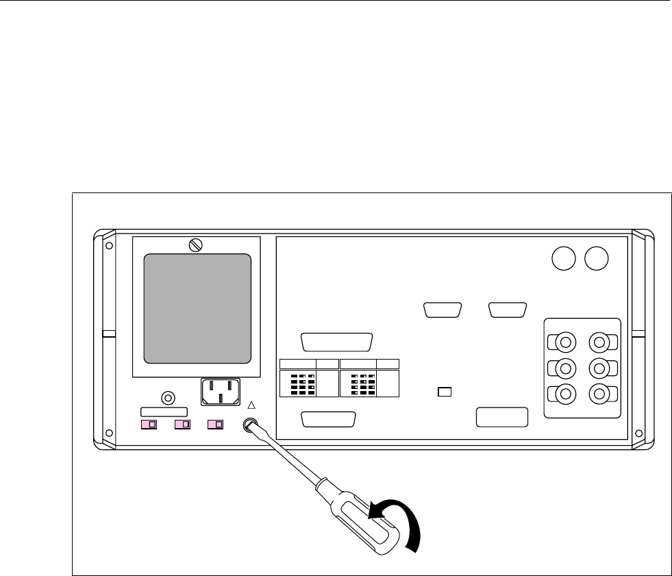
5700A/5720A Series II Calibrator
Service Manual
3-4
3-2. Accessing the Fuse
The fuse is accessible from the rear panel. The fuse rating label to the right of the fuse
holder shows the correct replacement fuse ratings for each operating voltage. To access
the fuse, refer to Figure 3-1 and proceed as follows:
1. Disconnect line power.
2. Using a standard screwdriver, turn the fuse holder counterclockwise until the cap
and fuse are disengaged.
VOLTAGE
SELECTION FUSE-F1
T 125A
250V
(SB)
100V S2 S3 S4
110V
115V
120V
VOLTAGE
SELECTION FUSE-F1
T 125A
250V
(SB)
200V S2 S3 S4
220V
230V
240V
CHASSIS
GROUND
S2 S3 S4
FUSE -F1
!
F7-1.EPS
Figure 3-1. Accessing the Fuse
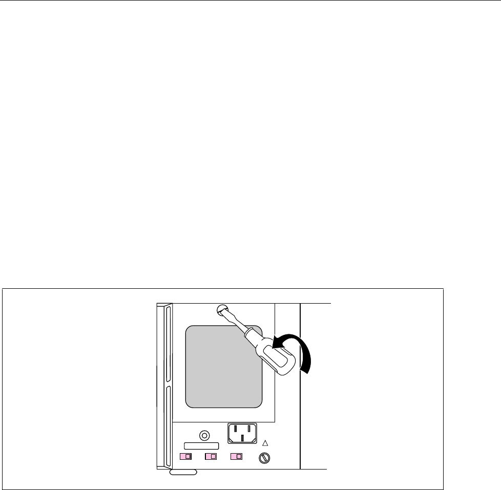
Calibration and Verification
Cleaning the Air Filter
3
3-5
3-3. Cleaning the Air Filter
Caution
Damage caused by overheating may occur if the area around
the fan is restricted, the intake air is too warm, or the air filter
becomes clogged.
The air filter must be removed and cleaned at least every 30 days, or more frequently if
the calibrator is operated in a dusty environment. The air filter is accessible from the rear
panel of the calibrator.
To clean the air filter, refer to Figure 3-2 and proceed as follows:
1. Disconnect line power.
2. Remove the filter by unscrewing the knurled screw at the top of the air filter pulling
the filter’s retainer downwards (it hinges at the bottom) and removing the filter
element.
3. Clean the filter by washing it in soapy water. Rinse and dry it thoroughly before
reinstalling.
4. Reinstall the filter and the knurled screw.
CHASSIS
GROUND
S2 S3 S4
FUSE -F1
!
F7-2.EPS
Figure 3-2. Accessing the Air Filter

5700A/5720A Series II Calibrator
Service Manual
3-6
3-4. Cleaning the Exterior
To keep the calibrator looking like new, clean the case, front panel keys, and lens using a
soft cloth slightly dampened with either water or a non-abrasive mild cleaning solution
that is not harmful to plastics.
Caution
Do not use aromatic hydrocarbons or chlorinated solvents for
cleaning. They can damage the plastic materials used in the
calibrator.
3-5. Calibration
This chapter provides procedures for calibrating the 5700A/5720A Series II to external
standards, adjusting the range if necessary, and for performing a calibration check.
Your calibrator is calibrated at the factory with constants that are traceable to NIST. In
order to maintain traceability, you only need to met the following requirements.
• Calibration to external standards must be completed at the beginning of the
calibration cycle
• Performance verification must be completed every two years.
• Zero Calibration must be performed every 30 days (refer to the 5700A/5720A Series
II Operators Manual).
Calibration check and range calibration are optional procedures that are provided for
enhancing the accuracy if needed for special requirements.
3-6. Calibrating the 5700A/5720A Series II to External Standards
You must calibrate to external standards at the beginning of the calibration cycle. The
length of the cycle (24 hours, 90 days, 180 days, or one year) is selected in a setup menu
described in Chapter 4 of the 5700A/5720A Operators Manual.
To calibrate the 5700A/5720A Series II, you apply three portable standards to the output
binding posts: a 10V dc voltage standard, a 1Ω resistance standard, and a 10 kΩ
resistance standard. The following standards are recommended:
• Model 732B DC Reference Standard
• Model 742A-1 1Ω Resistance Standard
• Model 742A-10k 10Ω Resistance Standard
Use the following Low Thermal Leads for all connections:
• When calibrating the 5700A, use either the connector set 5440A-7002 (banana
plugs) or the set 5440A-7003 (spade lugs).
• When calibrating the 5720A, use the set 5440A-7003 (spade lugs).
Warning
Operator accessible LETHAL VOLTAGES may be present on
the lugs at the end of these cables when used with
instrumentation capable of producing such voltages. These
cables should be used only when thermal emf performance is
required. For other applications, cables with operator
protection form contact with high voltages should be used.

Calibration and Verification
Calibrating the 5700A/5720A Series II to External Standards
3
3-7
3-7. Calibration Requirements
Both the calibrator and the recommended external standards have the ability to internally
control (or compensate for) ambient temperature variations. Therefore it is unnecessary
to keep the calibrator in tightly controlled temperatures during calibration. During the
calibration procedure, the calibrator prompts you to enter the ambient temperature, and
includes this information in specification readouts and output shift reports.
3-8. When to Adjust the Calibrator’s Uncertainty Specifications
Table 3-1 lists each external standard’s uncertainty limit, and the 5700A/5720A Series II
uncertainty specifications that must adjusted accordingly if that limit is exceeded.
As long as the external standards have the uncertainties listed in Table 3-1, you do not
need to adjust the calibrator’s absolute uncertainty specifications in Chapter 1. However,
if your standard’s uncertainty exceeds the value in the table you must adjust some of the
calibrator’s absolute uncertainty specifications by the algebraic difference between your
standard’s uncertainty and the uncertainty limit listed in the Table 3-1. For example, if
the dc voltage standard has an uncertainty of ±2.5 ppm, then the 5700A and the 5720A
absolute uncertainty specifications listed in Table 3-1 for the traceable quantity of
voltage must all be increased by ±1 ppm.
Table 3-1. Standards for Calibrating 5700A/5720A Series II
Fluke
Standard
Traceable
Quantity
Nominal
Value
Uncertainty
Limit
5700A/5720A Series II
Specifications susceptible to
Uncertainty Limit
732B Voltage 10V ±1.5 ppm dc volts, ac volts,
dc current, ac current
742A-1 Resistance 1Ω±10 ppm 1Ω, 1.9Ω
742A-10k Resistance 10 kΩ±4 ppm ac current, dc current 10Ω to
100 MΩ
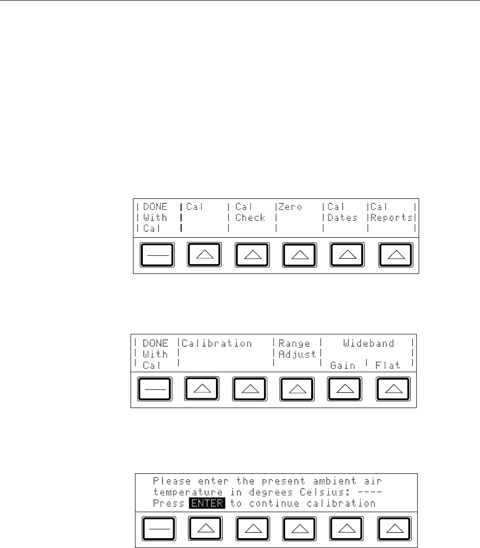
5700A/5720A Series II Calibrator
Service Manual
3-8
3-9. Calibration Procedure
Before you being this procedure make sure the calibrator is powered on and has
completed the appropriate warm-up period.
After you have finished calibration, but before you save the new constants, the calibrator
presents the new changes as ± ppm, and as a percentage of specifications for each range
and function. A list of changes can be sent to a computer through either the serial or
instrument control (IEEE-488) port, or printed through the serial port. The largest
proposed change will be displayed on the calibrator’s front panel.
Follow this procedure to calibrate the main output functions.
1. Press the “Setup Menus” softkey; then press the “Cal” softkey. The calibration menu
appears as shown below:
PREV
MENU
IF3-1.EPS
2. Press the “Cal” softkey. The display shows the following.
PREV
MENU
3. To calibrate the main output functions, press one of the softkeys under “Calibration.”
The display shows the following:
PREV
MENU
IF3-3.EPS
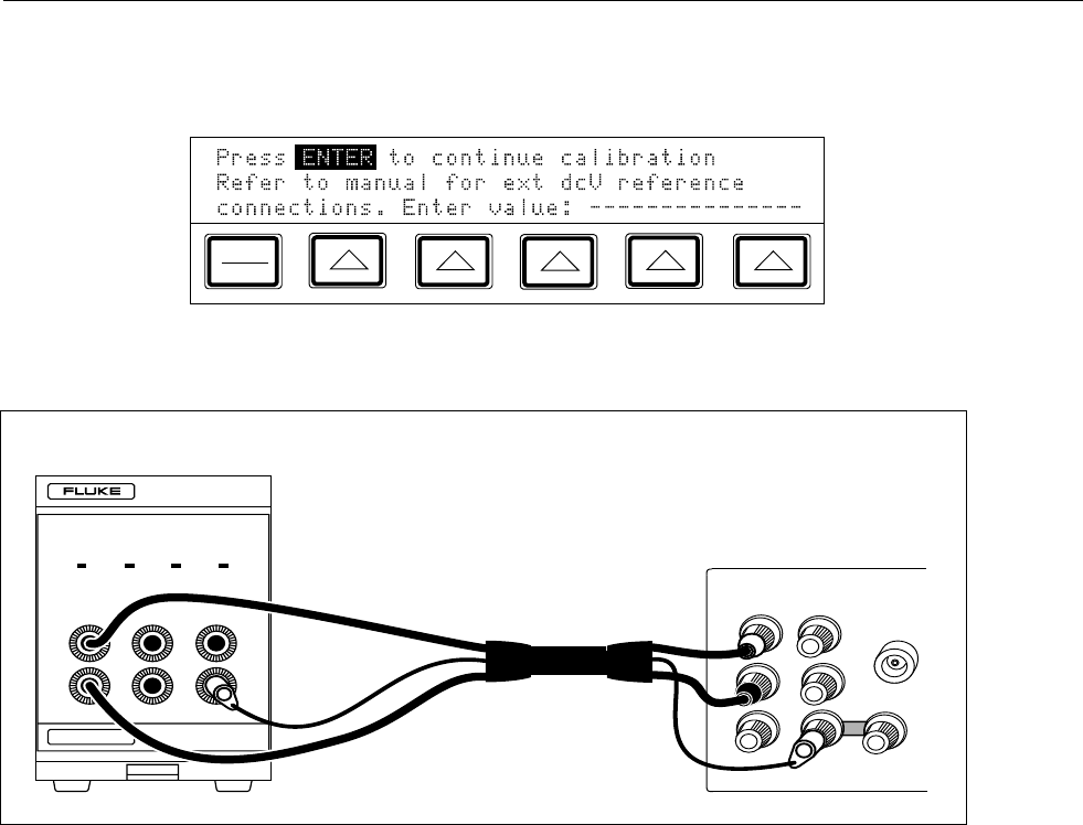
Calibration and Verification
Calibrating the 5700A/5720A Series II to External Standards
3
3-9
4. Enter the ambient temperature; then press E. The display shows:
PREV
MENU
IF3-4.EPS
5. Connect the 732B to the calibrator as shown in Figure 3-3.
732B DC STANDARD
AC PWR IN CAL CHARGE LOW BAT
10V 1.018V CHASSIS
GUARD1.018V COM10V COM
SERIAL NUMBER
HI HI
LO LO
HI
OUTPUT
V A
SENSE
V
AUX
CURRENT GUARD
GROUND
WIDEBAND
ΩΩ
CALIBRATOR
VOLTAGE REFERENCE
STANDARD
F7-3.EPS
Figure 3-3. 732B External Calibration Connections.
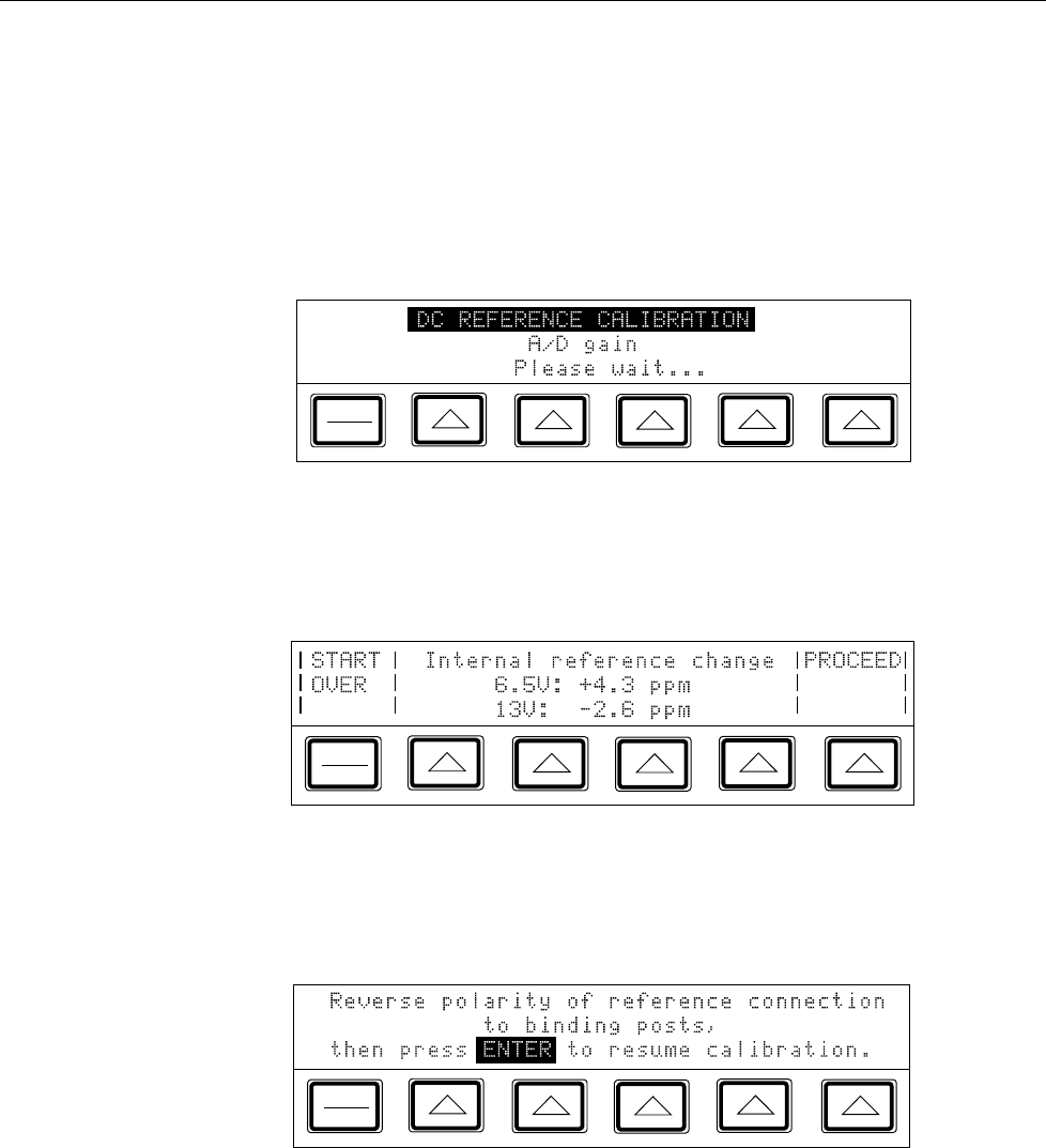
5700A/5720A Series II Calibrator
Service Manual
3-10
6. Enter the true value of the 732B 10V output. The true value is the value printed on
the calibration sticker, plus or minus, as well as drift that has occurred since
calibration. That drift can be estimated provided control charts have been maintained
for the 732B.
If the entered value is not between 9V and 11V, and error message appears, which
lets you start over from this point with a calibrated 732B. Press E, and the
display shows the following:
PREV
MENU
IF3-5.EPS
When the calibrator’s 6.5V and 13V references have been characterized, the display
shows the following message, which lets you accept or reject the changes that are
about to be made to the calibration constants.
PREV
MENU
IF3-6.EPS
7. To reject the changes, return to the calibration menu shown in step 2 by pressing
P. Otherwise, press the softkey under “Proceed” to accept and save the changes,
and to open the display shown below, letting you continue with calibration.
PREV
MENU
IF3-7.EPS
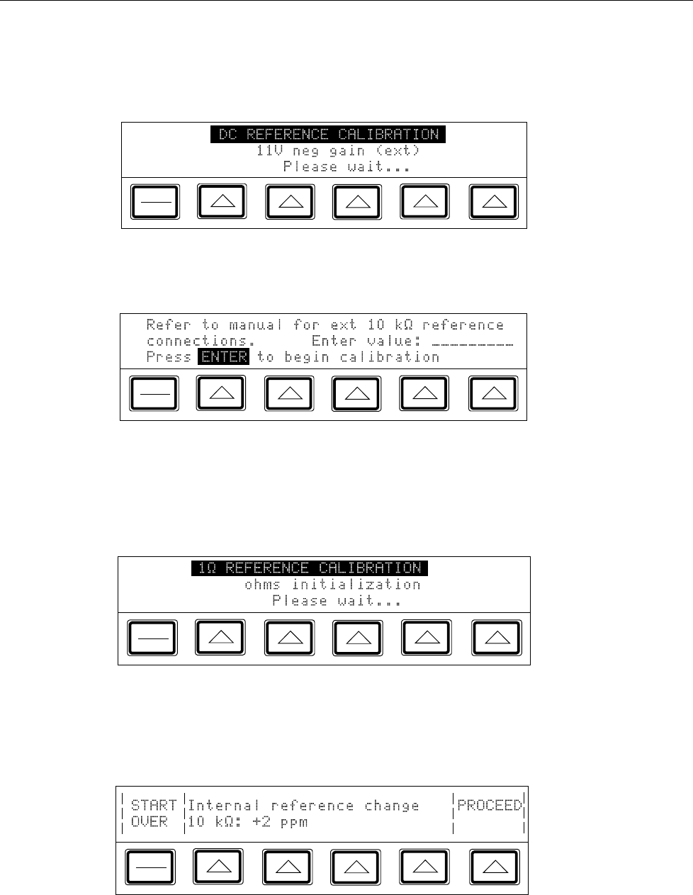
Calibration and Verification
Calibrating the 5700A/5720A Series II to External Standards
3
3-11
8. Reverse the HI and LO connections at the 732B terminals, and press E. The
following displays appear, asking you to wait before proceeding with the 10 kΩ
standard.
PREV
MENU
IF3-8.EPS
After a few seconds, the following display appears:
PREV
MENU
IF3-9.EPS
9. Connect the calibrator to the 10 kΩ standard as shown in Figure 3-4 and enter the
true value of the standard. If the standard is not between 9 kΩ and 11 kΩ, an error
message appears, which allows you to start over from this point with a different
standard. Press E again to open the following display:
PREV
MENU
IF3-10.EPS
When the internal 10 kΩ reference has been characterized, the following message
appears, which lets you accept or reject the changes that are about to be made to the
calibration constant:
PREV
MENU
IF3-11.EPS
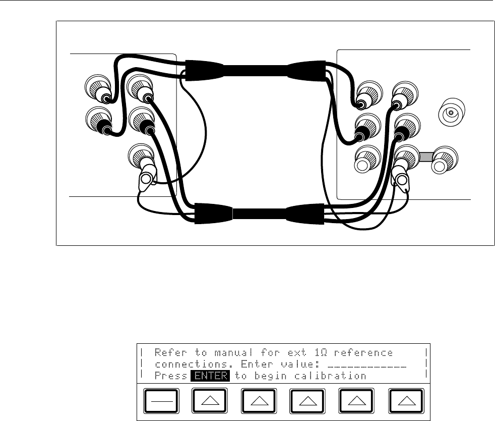
5700A/5720A Series II Calibrator
Service Manual
3-12
RESISTANCE STANDARD
HI
LO
HI
LO
SENSECURRENT
HI HI
LO LO
HI
OUTPUT
V A
SENSE
V
AUX
CURRENT
GUARD GROUND
WIDEBAND
CHASSIS
GROUND
ΩΩ
CALIBRATOR
F7-4.EPS
Figure 3-4. 742A-1 and 742A-10k External Calibration Connections
10. To reject the changes, return to the calibration menu shown in step 2 by pressing
P. Otherwise, press the softkey under “Proceed” to accept and save the changes,
and to open the display shown below, letting you continue with calibration.
PREV
MENU
IF3-12.EPS
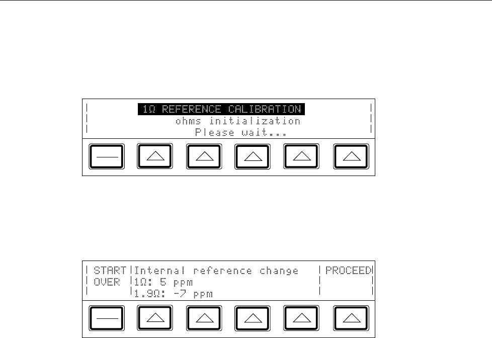
Calibration and Verification
Calibrating the 5700A/5720A Series II to External Standards
3
3-13
11. Disconnect the 10 kΩ standard, and connect the calibrator to the 1Ω standard; then
enter the true value of the 1Ω standard. If the standard is not between 0.9Ω and
1.1Ω, an error message appears, which lets you start over from this point with
another standard. Press E to bring up the following display:
PREV
MENU
IF3-13.EPS
When the internal 1Ω reference has been characterized, the following message
appears, which lets you accept or reject the changes that re about to be made to the
calibration constant:
PREV
MENU
IF3-14.EPS
12. To reject the changes, return to the calibration menu shown in step 2 by pressing
P. Otherwise, press the softkey under “Proceed” to accept and save the changes,
and let the calibrator complete the internal calibration steps.
13. The calibration is not effective until you store the newly calibrated constants in
memory. To store the constants, set the rear panel CALIBRATION switch to
ENABLE, the press the “Store Values” softkey.
Note
To review the proposed output shifts before you store the new constants,
print a listing of the proposed shifts by pressing the softkey under “Print
Output Shifts.”
14. After you store the constants, press the softkey under “DONE with Cal” to exit
calibration and resume normal operation.
15. If you press this softkey before you store the constants, the new constants will be
used temporarily for normal operation until the calibrator is powered down or reset.
(This is only true for software versions G and lower. For versions H and higher, the
process is aborted without updating existing constants.)
16. Set the rear panel CALIBRATION switch to NORMAL.

5700A/5720A Series II Calibrator
Service Manual
3-14
3-10. Range Calibration
Once calibration is complete, you may find you need to make further adjustments to the
range. Calibrating the range is accomplished by adjusting a range constant, which is an
additional gain multiplier. Although range calibration is not needed in order to meet total
uncertainty specifications, it is useful for tuning the calibrator so that its values are
closer to your own standards.
Use your own laboratory standard to adjust the range constants. The following procedure
for adjusting the range constants is designed for laboratory standard values that are
between 45% and 95% of the range’s full-scale value.
Once you adjust the range constant, the new constant remains active until the next
calibration, at which time all range constant multipliers are rest to 1. You can also erase
all range adjustments by calling up the format EEPROM menu and selecting Range
Constants (refer to Chapter 4 of the 5700A/5720A Operators Manual).
Before you begin the following procedure, make sure you have the equipment you need
on hand including your own laboratory standards where required.
The following example procedure adjusts the 220V dc range constant using the
following equipment:
• 732B DC reference standard
• 752A Reference Divider
• 845AB/845AR Null Detector
• Low Thermal Test Leads: 5440A-7002 (banana plugs) or 5440A-7003 (spade lugs)
Warning
Operator accessible LETHAL VOLTAGES may be present on
the lugs at the end of the 5440A-7003 cables when used with
instrumentation capable of producing such voltages. These
cables should be used only when thermal emf performance is
required. For other applications, cables with operator
protection form contact with high voltages should be used.
Proceed as follows to adjust the 220V dc range constant. You must have completed
calibration to external standards before you follow this procedure.
1. Press the “Setup Menus” softkey; the press the “Cal” softkey. The following menu
appears:
PREV
MENU
IF3-1.EPS
2. Press the “Cal” softkey to bring up the next menu shown below:
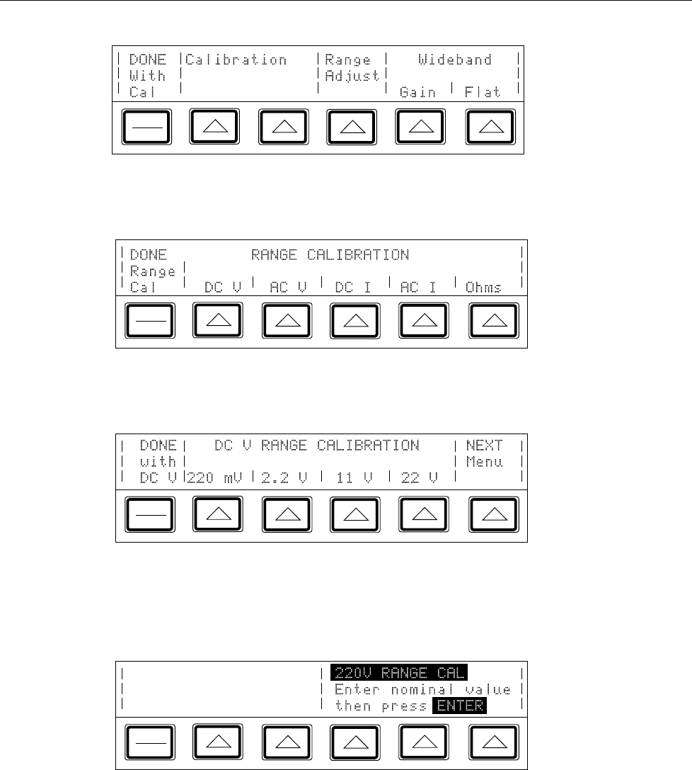
Calibration and Verification
Range Calibration
3
3-15
PREV
MENU
IF3-2.EPS
3. Press the “Range Adjust” softkey to bring up the next menu shown below:
PREV
MENU
IF3-18.EPS
4. Press the “DC V” softkey to bring up the next menu shown below:
PREV
MENU
IF3-19.EPS
5. Press the “NEXT Menu” softkey, which scrolls through all the available dc voltage
ranges, until 220V appears. Then press that selection’s softkey to open a display
similar to the following:
PREV
MENU
IF3-20.EPS
6. Connect the 732B, null detector, and 752A in a 10:1 configuration, as shown in
Figure 3-5.
7. Multiply the 732B’s value by 10, and enter this new value. (This value is the output
of the 752A, to which you will null the calibrator’s output.) Then press E to
bring up the following display.

5700A/5720A Series II Calibrator
Service Manual
3-16
PREV
MENU
IF057.EPS
8. Press O to activate the calibrator output. Then turn the output adjustment knob on
the calibrator until you achieve a null on the null detector.
9. Se the rear panel CALIBRATION switch to ENABLE. Press E on the front
panel. The calibrator will now calculate a new range constant multiplier for the 220V
dc range, and will store it in non-volatile memory.
10. The range calibration is now complete. Set the rear panel CALIBRATION switch to
the NORMAL position, disconnect the external standards, and press r to reset the
calibrator to its newly calibrated ranges.
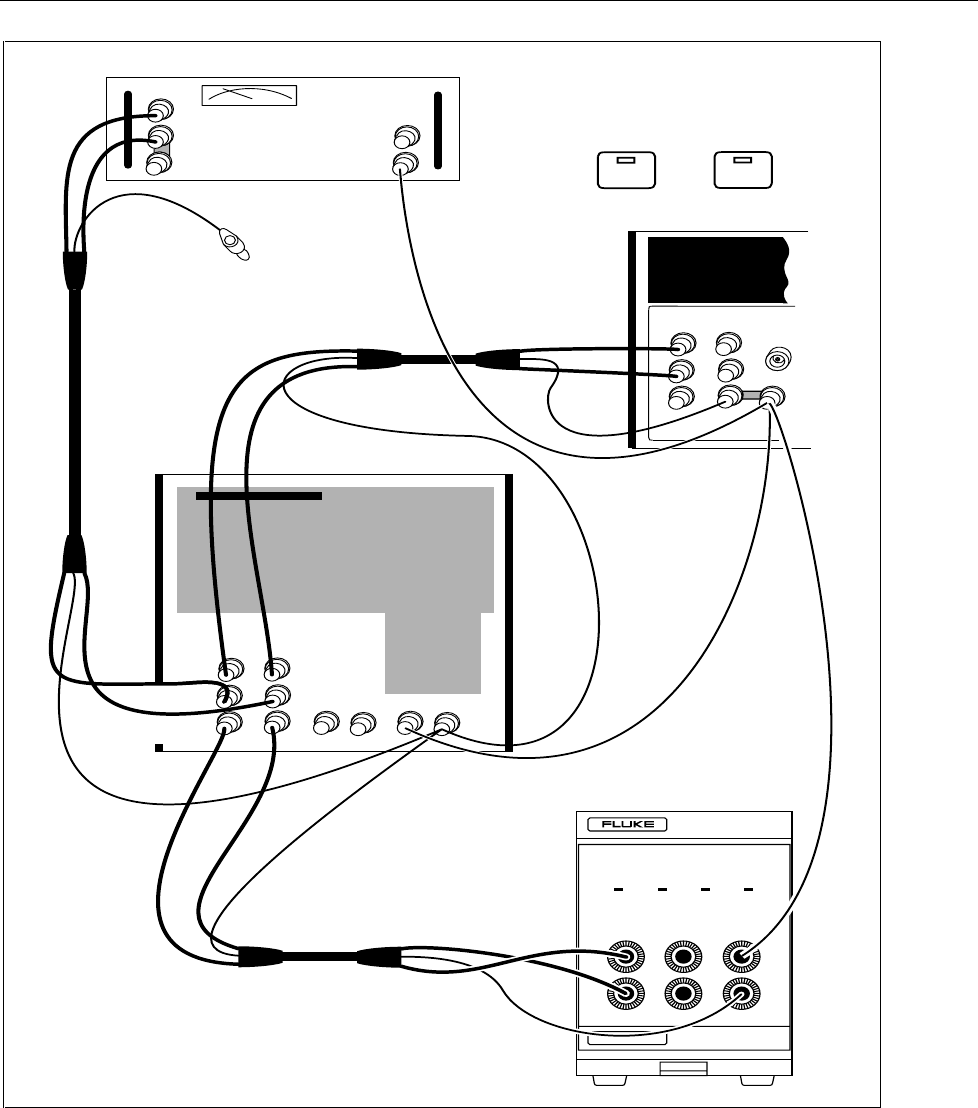
Calibration and Verification
Calibrating the Wideband AC Module (Option 5700A-03)
3
3-17
OUTPUT
V A
SENSE
VA
AUX
CURRENT GUARD
GROUND
WIDEBAND
NC
HI
HI
HI
LO
LO
LO OUTPUT
HI LO
GND GRD
752A VOLTAGE DIVIDER STANDARD
INPUT
REFERENCE
STANDARD
NULL
DETECTOR
HI
LO
GUARD GND
NULL DETECTOR
HI
LO
HI
HI
LO
732B VOLTAGE REFERENCE
STANDARD
EX SNS
: OFF
EX GRD
: OFF
Ω
CALIBRATOR
732B DC STANDARD
AC PWR IN CAL CHARGE LOW BAT
10V 1.018V CHASSIS
GUARD1.018V COM10V COM
SERIAL NUMBER
F7-6.EPS
Figure 3-5. 220V DC Range Calibration Connections
3-11. Calibrating the Wideband AC Module (Option 5700A-03)
The Wideband AC Module (Option 5700A-03) can be installed in either the 5720A or
5700A Series II calibrator. The module needs to be calibrated for both gain and flatness.
The gain should be calibrated when the 5700A-03 main output functions undergo their
routine calibration.
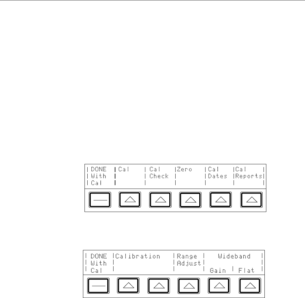
5700A/5720A Series II Calibrator
Service Manual
3-18
Since frequency flatness is determined by stable parameters (i.e. circuit geometry and
dielectric constants), the flatness of the Wideband AC Module has excellent long-term
stability. Consequently, a two-year calibration cycle is adequate for flatness calibration,
and can be scheduled to coincide with the calibrator’s shipment to a standards laboratory
for periodic verification.
The following procedure describes how to perform the wideband gain calibration.
Note
To perform this procedure you will need, in addition to the standard
equipment supplied with the wideband option, a Type “N” female to double
banana plug adapter (e.g., Pomona 1740).
Before you start this procedure, make sure the calibrator is powered on and has
completed an appropriate warm-up period. Then proceed with this procedure to calibrate
the wideband gain.
1. Press the “Setup Menus” softkey; then press the “Cal” softkey to being up the menu
shown below:
PREV
MENU
IF3-1.EPS
2. Press the “Cal “ softkey to bring up the following menu:
PREV
MENU
IF3-2.EPS
3. Connect the wideband output cable between the WIDEBAND connector and the
SENSE binding post.
The center conductor of the 50Ω feedthrough should go to SENSE HI and shown in
Figure 3-6. The GND tab on the adapter should be on the LO side.
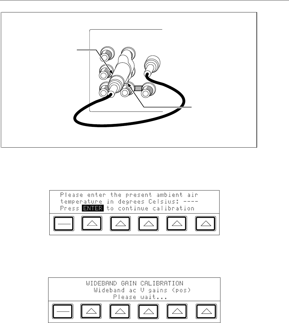
Calibration and Verification
Calibrating the Wideband AC Module (Option 5700A-03)
3
3-19
HI HI
LO LO
HI
OUTPUT
V A SENSE
V
AUX
CURRENT
GUARD GROUND
WIDEBAND
Ω
GND TAB
50 FEEDTHROUGH
Ω
Ω
CALIBRATOR
F7-5.EPS
Figure 3-6. Wideband Module Calibration Connection
4. Press the “Gain” softkey to bring up the following display:
PREV
MENU
IF3-3.EPS
5. Enter the ambient temperature; the press E. The display shows the
following:
PREV
MENU
IF3-15.EPS
As the wideband calibration proceeds, messages appear on the display identifying all
processes as they are encountered. When positive gains calibration is complete, a
message appears telling you to refer to the manual for negative gains connections.
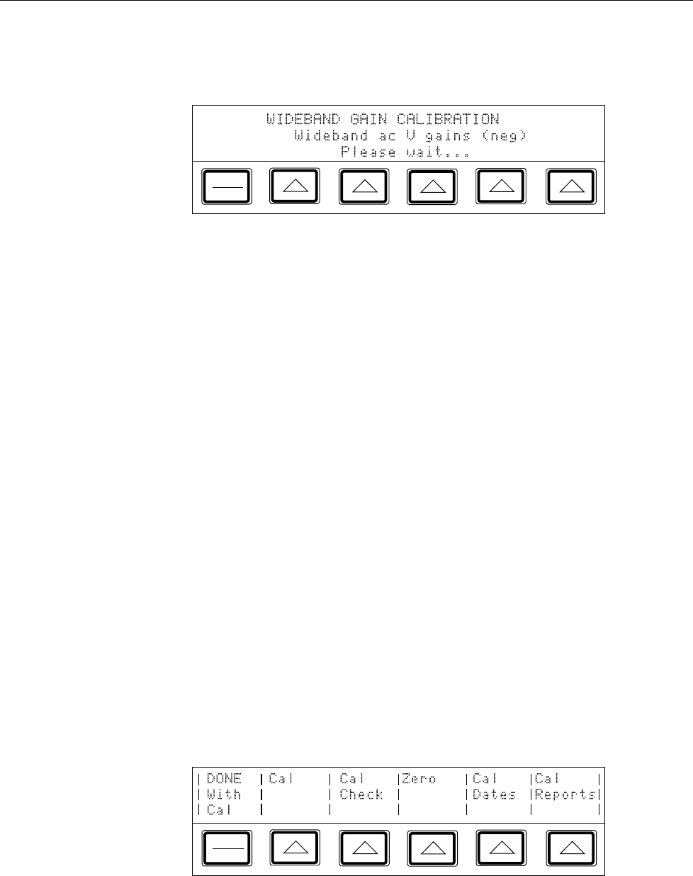
5700A/5720A Series II Calibrator
Service Manual
3-20
6. Reverse the dual-banana connector so that the center connector is connected to LO;
then press E. The display shows the following:
PREV
MENU
IF3-16.EPS
After a short time, a message appears indicating that the wideband calibration is
complete.
7. To store the new constants, set the CALIBRATION switch to ENABLE and press
“Store Values.” To discard the constants, press “DONE with Cal” and answer “YES”
when the display asks for verification.
8. You have now completed the wideband gain calibration. Set the CALIBRATION
switch to NORMAL, disconnect the wideband cable, and press r.
3-12. Performing a Calibration Check
A calibration check is similar to the calibration, with the primary difference being that
no changes are made to the stored constants, and the internal check standards are used as
the reference points. A calibration check produces a report similar to the normal
calibration report, and shows any proposed changes.
This procedure can be performed from an external computer, and can be set to run
automatically, with no assistance (there is no need to enable the CALIBRATION switch,
since no constants are changed).
You can use the calibration check at any time to confirm the integrity of the calibrator
without connecting external standards. The calibration check is also useful for collecting
a performance history.
Before you begin this procedure, make sure the calibrator is powered on and has
completed the appropriate warm-up period. Then follow this procedure to check the
calibration.
1. Press the “Setup Menu” softkey; then press the “Cal” softkey to bring up the
following menu:
PREV
MENU
IF3-1.EPS
2. Press the “Cal Check” softkey to bring up the following display:
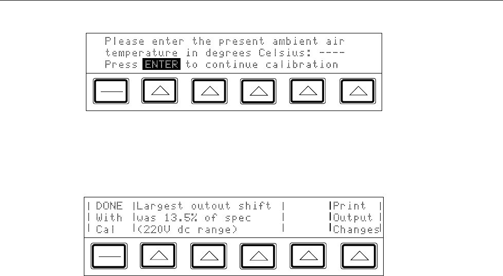
Calibration and Verification
Performing a Calibration Check
3
3-21
PREV
MENU
IF3-3.EPS
3. Enter the ambient temperature; then press E. As the calibration check
proceeds, the display indicates the current process of the calibration check. When the
check is complete, the largest shift that is detected appears on the display.
PREV
MENU
IF3-17.EPS
4. You can now print a list of the proposed shifts, or quit without creating a list.
To print the report, connect a printer and set up the serial interface as described in
Chapter 6 of the 5700A/5720A Operators Manual. Press the softkey under “Print
Output Changes.” To return to normal operation without printing, press the softkey
under “DONE with check.”
Press P to exit the calibration menus.

5700A/5720A Series II Calibrator
Service Manual
3-22
3-13. Full Verification
An independent external verification is recommended every two years, following normal
periodic calibration or repair of the calibrator. Verification establishes and maintains
parallel external traceability paths for the internal functions that are not adjusted or
corrected during calibration. An example is the internal ac/dc transfer standard.
Verification also serves as a check that internal calibration processes are in control.
Note
All performance limits specified in the test records apply to 90-day
specifications for the Calibrator. If limits to other specifications are
desired, the test records must be modified. A description of how to
determine a guardband test limits is included in this section.
Note
Equivalent equipment and methods, either manual or automated, may be
substituted for the following verification tests as long as the same points
are tested, and equipment and standards used are at least as accurate as
those specified. If standards are less accurate than specified, appropriate
tolerance limit and/or accuracy reductions must be made to achieve
equivalent results.
Not all of the procedures contained in this chapter need to be performed to verify your
calibrator. This chapter contains the verification procedures for the 5720A and the
5700A Series II Calibrators. In addition, procedures are provided to verify the ac
functions of the calibrator with a 5790A. The following roadmap provides a high-level
overview of the verification tests discussed in this chapter.
5720A 5790A
5700A 5790A
Resistance
3-16 3-22 3-26 3-28
to
3-30
3-22 3-26 3-28
to
3-30
3-18 3-20 3-21
3-16 3-18 3-20 3-21
DC
Volt
AC
Volt
AC
Current
Wide
Band
DC
Current Frequency
Resistance DC
Volt
AC
Volt
AC
Current
Wide
Band
DC
Current Frequency
F0-0.EPS
Figure 3-7. Overview of Verification Tests

Calibration and Verification
Full Verification
3
3-23
In Figure 3-7, the location of each test is identified by the paragraph numbers.
3-14. Required Equipment for All Tests
An abbreviated summary of required equipment for all the verification and optional tests
is given in Table 3-2. Individual lists of required equipment are included at the
beginning of each test. For substitution information, refer to Table 3-15, Minimum Use
Requirements, located near the end of this section.
3-15. Warm-up Procedure for All Verification Tests
Before performing verification, do the following preliminary steps:
1. Verify that the Calibrator has warmed up for at least thirty minutes.
Note
If the Calibrator has been powered off in an environment outside of
operating environment specifications, particularly with humidity above
70%, allow a minimum of two hours warm-up. Extended storage at high
temperatures and humidity may require up to four days of power-on
stabilization.
2. If you are doing a regularly scheduled full verification as recommended by Fluke,
calibrate the 5700A/5720A Series II as previously described before continuing with
verification.
3. Ensure that each piece of external test equipment has satisfied its specified warm-up
requirements.
4. Ensure that the Calibrator is in standby (STANDBY annunciation lit).

5700A/5720A Series II Calibrator
Service Manual
3-24
Table 3-2. List of Required Equipment for Main Output
Equipment Description Application
AC Measurement Standard or Fluke 5790A ACV, ACI
Resistance Standards Fluke 742A Series Cal, Ohms, DCI
Reference Divider Fluke 752A DC V
Null Detector EM Electronics N11 (Fluke 845A) DC V
Shunt Adapter Fluke 792A-7004 AC I
Calibrator Fluke 55X0A Ohms
Frequency Counter Philips PM6669 Frequency
Shunts Fluke A40 Series AC I
High Current Shunt Fluke Y5020 DC I
Resistance Standard L&N 0.1Ω 4221B DC I
DMM Wavetek 1281 or HP 3458A Ohms, DCI, ACI, AC V
Low Thermal Cables Fluke 5440A-7002 (5700A) or
5440A-7003 (5720A or 5700A)
Various
Equipment Required for Wideband Ac Module (Option 5700-03) Verification
Equipment Description Application
AC Measurement Standard Fluke 5790A with Wideband
Option -03
Wideband
Wideband Cable (supplied with
5700A-03)
Fluke Cable Wideband
50Ω Termination (supplied with
5700A-03)
Fluke Termination Wideband
Adapter (supplied with 5700A-03) Pomona 1269 BNC(F) to dual
banana plug
Wideband
Adapter Kings KN-99-46 N(F) to BNC(M) Wideband
Equipment Required for Optional Tests
Equipment Description Application
Oscilloscope Mainframe Tektronix 7000 Series HF Noise
Differential Amplifier Tektronix 7A22 HF Noise
Distortion Analyzer Krohn-Hite 6900B AC V, ACI, Distortion
Spectrum Analyzer HP 8590A AC V, Wideband
Distortion
Kelvin Varley Divider Fluke 720A DC V Linearity

Calibration and Verification
Full Verification
3
3-25
3-16. Resistance Verification Test
The following test requires testing at the high, low and intermediate values only. This is
because the 5700A/5720A Series II creates the other values of resistance from these
values. Use Tables 3-16 (5720A) and 3-17 (5700A) for test records. For the convenience
of anyone wishing to test the intermediate values, the tolerance limits are included.
Testing these values could be done using a Hamon-type ratio device and a very stable,
high-resolution bridge or DMM, or a combination of the two. Table 3-3 lists equipment
required for this test. See Table 3-15, Minimum Use Requirements, for substitution
information.
Table 3-3. Equipment Required for Resistance Testing
Equipment Decsription
Resistance
Standards
Fluke 742A Series in the following values: 1Ω, 1.9Ω, 10Ω, 10 kΩ, 19 kΩ, 10 MΩ,
and 19 MΩ
Current Source Fluke 5500A or 5520A
DMM Wavetek 1281 or HP 3458A
1. Connect the equipment as shown in Figure 3-8.
2. Set the Calibrator output to 1Ω with external sensing (EX SENS indicator lit) and set
the dc DMM to read dc V. Record the 1Ω resistance standard value on the test record
as the 1Ω STD RES VALUE.
3. Multiply the certified value of the 1Ω resistance standard by 0.1 and record the result
on the test record as the 1Ω STD VOLTAGE.
4. Connect the DMM across the sense terminals of the 1Ω resistance standard.
5. Set the direct current source for a nominal 100 mA output. Vary the source until the
DMM reading is as close as possible to the 1Ω Standard Voltage recorded in the
previous step. Record the DMM voltage reading on the test record as the
MEASURED 1Ω STD VOLTAGE.
Note
If the current source used has the resolution to achieve a voltage reading
to within ±5 ppm of the value in step 3, it is not necessary to calculate the
cal current in take next step. In this case, when you come to step 9 you
will simply multiply the voltage reading from step 9 by a factor of 10,
which is the same as dividing by 100 mA (0.1A).
6. Calculate the exact current by dividing the MEASURED 1Ω STD VOLTAGE by the
1Ω STD RES VALUE; record the result on the test record as the CAL CURRENT.
7. Enter the Calibrator displayed 1Ω value on the test record as the UUT 1Ω
DISPLAYED VALUE.
8. Transfer the dc DMM leads to the Calibrator sense terminals.
9. Enter the DMM voltage reading on the test record as the UUT 1Ω VOLTAGE.
10. Calculate the UUT true 1Ω resistance by dividing the UUT 1Ω VOLTAGE by the
CAL CURRENT.
11. Adjust the output adjustment knob for a UUT Control Display reading equal to the
true 1Ω resistance value calculated in the previous step. The error from the displayed
value is also shown on the Control Display. Enter the value of the error on the test
record as the UUT DEVIATION FROM DISPLAYED VALUE.
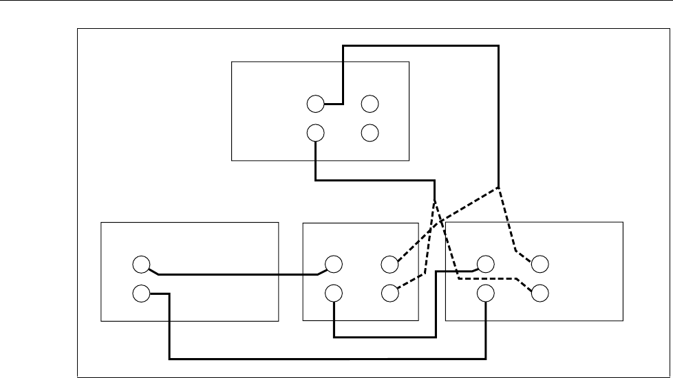
5700A/5720A Series II Calibrator
Service Manual
3-26
INPUT SENSE
HI
LO
HI
LO
DMM
OUTPUT SENSE
HI
LO
HI
LO
CALIBRATOR
(UUT)
CURRENT SENSE
HI
LO
HI
LO
OUTPUT
HI
LO
CURRENT SOURCE 742A-X
F3-5.EPS
Figure 3-8. 1 Ohm and 10 Ohm Resistor Verification
Note
There is no need to do the cal current calculation of step 6 if the current
source has a settability of ±3 ppm.
12. Repeat steps 3 through 11 for the 1.9Ω and 10Ω resistance values using the 1.9Ω and
10Ω resistance standards. At the 10 ohm check, use 10 mA of current and a
multiplier for step 3 of 0.01.
13. The low-value (1Ω, 1.9Ω, and 10Ω) tests are summarized in Table 3-4.

Calibration and Verification
Full Verification
3
3-27
Table 3-4. Low Value Resistance Calibration Using a Current Source
5720A (UUT)
Resistance Apply Current 5720A Deviation From
Displayed Value (90-day) 5720A Displayed Value
1Ω100 mA ±95 ppm 0.9995 to 1.0005
1.9Ω100 mA ±95 ppm 1.89905 to 1.90095
10Ω10 mA ±25.0 ppm 9.997 to 10.003
5700A (UUT)
Resistance Apply Current 5700A Deviation From
Displayed Value (90-day) 5700A Displayed Value
1Ω100 mA ±95 ppm 0.9995 to 1.0005
1.9Ω100 mA ±95 ppm 1.89905 to 1.90095
10Ω10 mA ±28.0 ppm 9.997 to 10.003
14. For the remaining tests, no current source is required. Verify that each true UUT
value is within the limits shown in Table 3-16 for 5700A and Table 3-17 for 5720A.
a. Connect the DMM, set for 4-wire resistance, first to the Resistance Standard
equal to the UUT nominal output and then to the UUT itself. In each case, record
the resistance standard DMM reading and the resistance standard certified value.
b. Calculate the DMM correction by subtracting the DMM reading from the
certified value; enter this calculated value on the test record as DMM ERROR.
c. Move the DMM to the UUT terminals; enter the DMM reading on the test record
as DMM UUT RES RDG.
d. Algebraically add the DMM ERROR and the DMM UUT RES RDG; enter the
sum on the test record as UUT TRUE RES VALUE.
e. Adjust the output adjustment knob for a UUT Control Display reading equal to
the true resistance value previously calculated. The error from the displayed
value is also shown on the Control Display. Enter this error (with polarity
reversed) on the test record as the UUT DEVIATION FROM DISPLAYED
VALUE.
3-17. Two-Wire Compensation Verification
Use the following steps to verify that two-wire compensation operates correctly:
1. Connect the UUT (output set to 100Ω, with external sensing) to the DMM (set for 4-
wire resistance measurement). Note the DMM reading.
2. Connect two shorts: DMM SOURCE HI to SENSE HI and DMM SOURCE LO to
SENSE LO.
3. Activate UUT 2-wire compensation.
4. Check that the DMM reading returns to within 4 miliohms of the reading noted in
step 1.

5700A/5720A Series II Calibrator
Service Manual
3-28
3-18. DC Voltage Verification Test
The following test checks every dc voltage range by testing the output accuracy at
decade values of voltage from 100 mV to 1000V. Use Table 3-18 (5720A) or Table 3-19
(5700) for the test record. Table 3-5 lists equipment required for this test as well as the
Linearity Test that follows. See Table 3-15, Minimum Use Requirements, for equipment
substitution information.
Table 3-5. Equipment Required for DC Voltage Testing
Equipment Model
DC Reference Standard Fluke 732B
Reference Divider Fluke 752A
Null Detector EM Electronics 11 (Fluke 845A)
Low Thermal Cables 5440A-7002
5440A-7003
Note
The 5440A-7002 or 5440A-7003 is for the 5700A; the 5720A uses only the
5440A-7003.
Proceed as follows to perform the dc voltage verification test:
1. Self-calibrate the reference divider in accordance with its instruction manual prior to
proceeding.
2. Connect the equipment as shown in Figure 3-5.
3. Set the reference divider to 0.1V. Set the Calibrator to the certified value of the dc
reference standard divided by 100. For example, if the certified value of the dc
reference standard is 10.000007V, set the Calibrator to 100.00007 mV.
4. Press OPR/STBY. After the reading has settled, verify that the null detector reads 0V
±1.20 µV (5720A 90-day specification) or 0V ±1.45 µV (5700A 90-day
specification). Set the Calibrator to standby.
5. Repeat the above process to test each dc voltage range output listed in Tables 3-23 or
3-24. (0.1V is in the table for completeness; you do not need to repeat it.) After the
null detector reading stabilizes, ensure that any observed meter rattle (over and
above the null detector rattle in the "zero" position) over a ten-second period does
not exceed the amount shown in the last column. In each case, set the 5720A to
standby before changing to the next voltage settings and go back to operate before
reading the null detector.
6. Reverse the connections of the dc reference standard at the reference divider and
repeat the previous measurement process for the -0.1V, -1V and -10V outputs.

Calibration and Verification
Full Verification
3
3-29
3-19. DC Voltage One-Tenth Scale Linearity Test
Note
If the result of the previous test at 1V on the 11V range was less than
2.5
µ
V it is not necessary to perform this test.
This test uses the same equipment as the previous test. Proceed as follows to perform the
DC Voltage One-Tenth Scale Linearity Test:
1. Set the reference divider range to 10V. On the voltage reference standard, remove
the lead from the 10V high terminal and connect it under the binding post of the low
terminal along with the low lead to provide a 0V reference input to the reference
divider. Set the Calibrator output for 10V, then activate range lock for the 11V
range. Now set the Calibrator to 0V OPERATE.
2. Note the reading on the null detector. Press OFFSET on the Calibrator. Return the
lead on the voltage reference to the high output terminal.
3. Set the Calibrator to 10V. Use the Calibrator output adjustment knob to obtain the
reading previously noted on the null detector. Press SCALE on the Calibrator.
4. Set the Calibrator to 1V dc. Set the reference divider to the 1V range, and verify that
the null detector indicates less than 2.5 µV from the noted reading.
5. Press RESET on the Calibrator. This completes the DC Voltage Calibration
Verification testing.
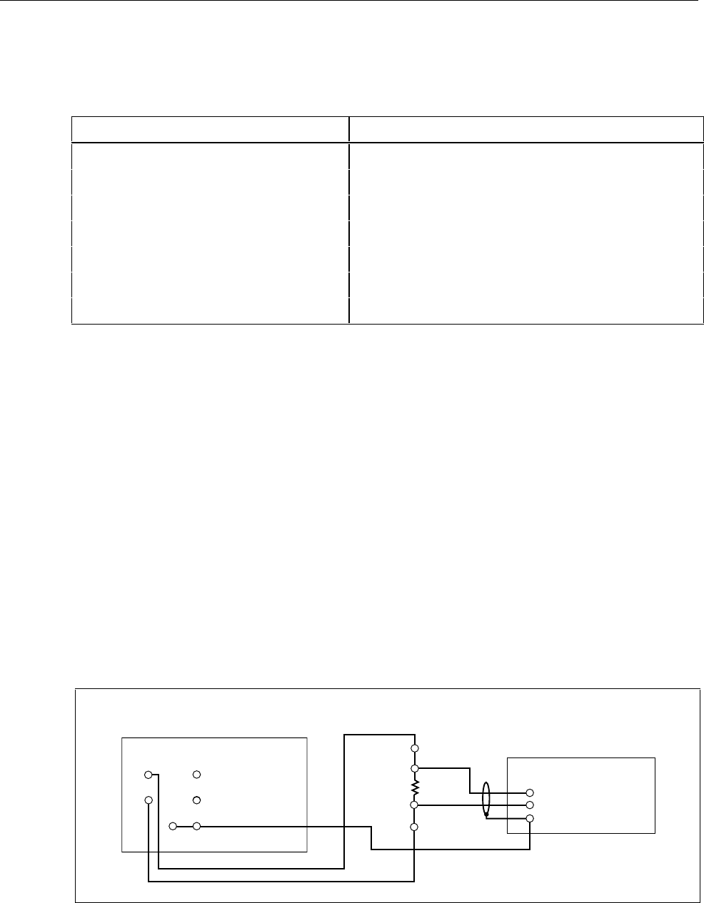
5700A/5720A Series II Calibrator
Service Manual
3-30
3-20. Direct Current Accuracy Verification Test
Equipment required for the Direct Current Accuracy Verification Test is listed in Table
3-6. Proceed as follows to test accuracy of the dc current function:
Table 3-6. Equipment Required for Direct Current Test
Equipment Model
DC DMM, 6-1/2 digit Wavetek 1281 or HP 3458A
High-Current Shunt Fluke Y5020 (for 5725A only)
Resistance Standards L&N 4221B (0.1Ω at 2A)
Fluke 742A-1 (1Ω at 200 mA)
Fluke 742A-10 (10Ω at 20 mA)
Fluke 742A-1k (1 kΩ at 2 mA)
Fluke 742A-10k (10 kΩ at 200 µA)
Use Table 3-20 (5720A) and Table 3-21 (5700A) for the test records.
1. Connect the dc DMM to the Calibrator output and set the Calibrator for outputs of
200 mV, -200 mV, 2V, and -2V, and record the dc DMM reading at each voltage in
Table 3-20 or 3-21.
2. Refer to the resistance standard test report and enter the corrections for all the
certified values in ± ppm in column A on the test record.
Note
The STD RES CORRECTION is the difference between the nominal
standard resistor value and the certified or true resistor value. For
example, if the nominal value is 0.1
Ω
and the certified value is
0.0999963
Ω
, the difference equals 0.0000037
Ω
, or +37 ppm.
3. Connect the equipment as shown in Figure 3-10 using the L&N 0.1Ω resistor.
4. Set the Calibrator for a 2A dc output, and adjust the Calibrator using the output
adjustment knob to obtain the characterized voltage reading on the dc DMM. Wait 3
seconds, and record the Calibrator error display reading in ± ppm (Column B).
LO
OUTPUT SENSE
HIHI
LO
CALIBRATOR (UUT)
HI
LO
SHUNT
USE INTERNAL GUARD
DC DMM
GND
GRD
INPUT
F3-7.EPS
Figure 3-9. Direct Current Accuracy Test Setup
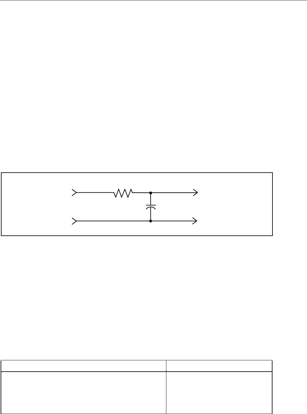
Calibration and Verification
Full Verification
3
3-31
5. Algebraically add column B to column A. Enter the result on the test record. Verify
that it is within the test limits shown.
6. Repeat steps 2 through 5 using the Fluke 742A Resistance Standards and Calibrator
output currents shown in Tables 3-25 or 3-26.
7. If the Calibrator is attached to a 5725A Amplifier, connect the Y5020 high-current
shunt to the 5725A output terminals. Connect the dc DMM to the Y5020 high-
current shunt voltage output connector.
8. Set the Calibrator to 10A, -10A, 5A, 3A and -3A and record the dc DMM readings
on the 5725A Amplifier dc current test record. Divide these readings by the certified
value of the Y5020 high current shunt, record the resultant current and verify that it
is within the test limit shown.
3-21. AC Voltage Frequency Accuracy Test
This test requires the use of a frequency counter. Philips model PM6669 is
recommended. Use Table 3-22 for the test record. When using Philips Model PM 6666,
it is recommended to use a 1 MHz Low Pass Filter as shown in Figure 3-10. Refer to
Table 3-15, Minimum Use Requirements, for substitution information.
1.59 kΩ Resister
Metal Film P/N 344341
Calibrator Main
Output Terminals
10 pF
Capacitor
P/N 713875
PM6666
Input A
Mount components on a duel banana adapter from ITT Pomona. Part Number 1837
F3-6A.EPS
Figure 3-10. 1 MHz Low Pass Filter
To check the Calibrator frequency accuracy, proceed as follows:
1. Connect the frequency counter to the output terminals of the Calibrator.
2. Set the Calibrator to 1V at the output frequencies listed in Table 3-22. Verify that the
counter reads within the limits shown on the test record.
3. Disconnect the counter from the Calibrator.
3-22. Output Level Tests For AC V Ranges
This test requires the use of equipment listed in Table 3-7.
Table 3-7. Equipment Required for AC V Output Level Tests
Equipment Model
AC Measurement Standard Fluke 5790A
BNC(F) to Dual-Banana Plug Adapter (2 required) Pomona 1269
Coax Cable - RG-58A/U or RG-58C/U with BNC(M)
Connectors, 12 ± 1 inch Long
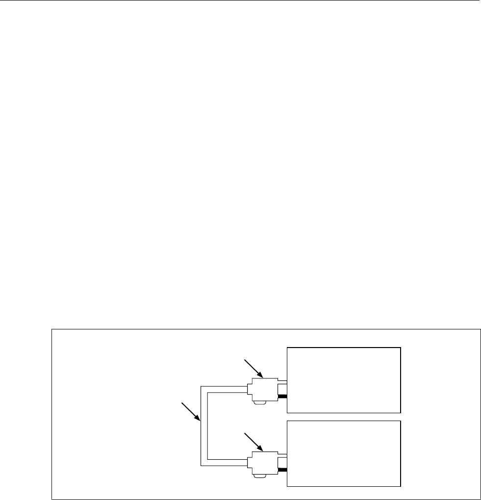
5700A/5720A Series II Calibrator
Service Manual
3-32
Use Table 3-23 (5720A) or Table 3-24 (5700A) for the test records.
1. Place the 5790A on top of the Calibrator and connect the equipment as shown in
Figure 3-11.
Note
The point of measurement is at the end of the cable and adapter that
connects to the 5790A. Other cable lengths and adapters will yield
different results at high frequencies.
2. On the 5790A push UTIL MENUS button and then the MEAS CONTROL softkey.
Set the digital filter mode to FAST and the restart to MEDIUM. Push the DONE soft
key twice to return to the measurement display.
3. Set the 5790A to 2 mV at 1 kHz. Adjust the Calibrator using the output adjustment
knob for a reading of 2.0000 mV ±1 count on the 5790A. Record the Calibrator error
display reading in the 90 Day column in Table 3-23 (5720A) or 3-24 (5700A) as
appropriate for the verification interval.
4. Verify that the result is within the test limits.
5. Repeat the previous steps for the 2 mV output on all remaining frequencies on the
test record.
6. Proceed to the remaining output levels and frequencies list in Table 3-23 or 3-24 and
repeat steps 3 through 5 using the appropriate output level in each step, and the
adjustment tolerance in Table 3-8.
5790A Side View
HI
LO Input 2
Calibrator Side View
HI
LO Output
BNC to
Banana Adapter
12 Inch
Coax Cable
BNC to
Banana Adapter
F3-6.EPS
Figure 3-11. AC Voltage Test Setup

Calibration and Verification
Full Verification
3
3-33
Table 3-8. 5790A Adjustment Counts
5700A/5720A Series II Output
Level
5790A Display 5790A Adjustment Counts*
2 mV 2.0000 ±1
20 mV 20.0000 ±1
200 mV 200.0000 ±4
2V 2.000000 ±4
2.3V 2.30000 ±1
20V 20.00000 ±4
200V 200.0000 ±4
300V 300.000 ±1
600V 600.000 ±2
1000V 1000.000 ±2
*Adjustment counts of 3 times the listed value is allowed at 1 MHz
3-23. AC Current Test
,
22 mA to 11A Ranges
This test requires the use of equipment listed in Table 3-9, when using the 5790A Input
1. Use Tables 3-33 (5720A) or 3-34 (5700A) for a test record.
Table 3-9. Equipment Required for 22 mA to 11A Alternating Current Test Using the 5790A Input 1
Equipment Model or Description
AC Measurement standard Fluke 5790A
Current Shunts Fluke A40 Series: 20 mA, 200 mA, 2A, and A40A Series: 10A (if verifying a
5725A) , with AC-DC difference corrections.
Current Shunt Adapter Fluke 792A-7004 A40 current shunt adapter
Cable Pomona 1368-A-18. Double banana to single banana plugs.
Cable (For 10A Setup) Pomona 5268-C-12. BNC(M) to single banana plugs.
Cable (For 10A Setup) Fluke A45-4003 (PN 212853) UHF(M) to UHF(M) with RG8A/U cable
Adapter (For 10A Setup) Pomona Model 1707. UHF(F) to banana adapter.
Adapter (For 10A Setup) Kings KC-99-34 UHF(M) to BNC(F)
Adapter (For 10A Setup) Pomona Model 1707. UHF(F) to banana adapter.

5700A/5720A Series II Calibrator
Service Manual
3-34
1. Connect the equipment as shown in Figure 3-12(A) use the 2A shunt.
2. Enter the ac to dc difference corrections for each shunt at each frequency in the
appropriate column of the test record (Table 3-26 or 3-27).
3. Set the Calibrator for a +2A dc output. Adjust the output so that the error display is
equal to the UUT actual error for a +2A output, as shown on the dc current test
record in Table 3-20 (5720A) or Table 3-21 (5700A).
4. Push the INPUT 1 button on the 5790A if you are using the INPUT 1 setup, or the
SHUNT button if you are using the SHUNT set up. Let the 5790A settle on a
reading.
5. Push the SET REF soft key on the 5790A.
6. Set the Calibrator for a -2A dc output. Adjust the output so that the error display is
equal to the UUT actual error for a -2A output, as shown in Table 3-20 (5720A) or
Table 3-21 (5700A).
7. Press the AVG REF soft key on the 5790A after the 5790A reading settles.
8. Set the Calibrator to 2A at 40 Hz and OPERATE.
9. Record the error displayed on the 5790A in Table 3-26 or 3-27.
10. Return to the error corrected +2A DC output that was set in step 3 and verify that the
5790A display returns to a zero reading ±10 PPM. If necessary, repeat steps 3
through 9 until the required results are obtained.
11. Algebraically add the 5790A error display reading to the A40 Shunt ac to dc
difference, and verify that the result is within the specifications of the test limits.
Record the results on Table 3-26 (5720A) or Table 3-27 (5700A).
12. Change the Calibrator frequency to 1 kHz, 5 kHz and 10 kHz. At each frequency
record the 5790A error display. Verify the results as was done in steps 8 and 9.
13. Repeat steps 3 through 12 at currents of 200 mA and 20 mA using the appropriate
A40 current shunt at the frequencies shown on the test record (Table 3-26 or 3-27).
14. For units with a 5725A Amplifier attached, use the test set up shown in Figure
3-12(B) using the 10A shunt at the frequencies listed on the test record.
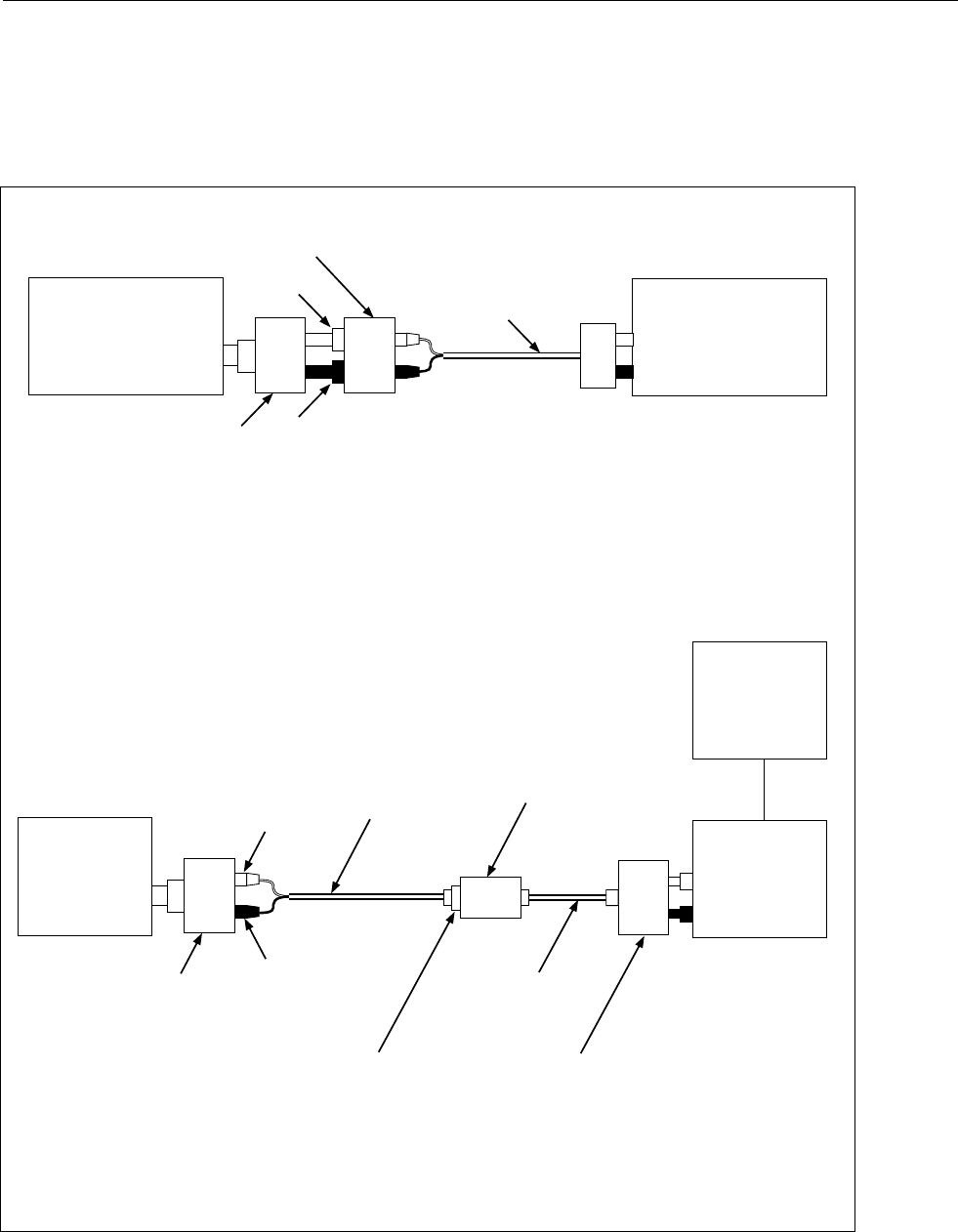
Calibration and Verification
Full Verification
3
3-35
Note
When verifying the 5725A Amplifier at the 10A level, allow sufficient time
for the A40A-10 shunt to reach thermal stability after initially applying the
current.
A. Alternating Current Test Setup, 22 mA to 2A Using 5790A Input 1
Hi
5790A
Input 1
Pomona Cable
1368-A-18
Lo
Red
Black
792A-7004
A40 Current Shunt Adapter
A40 Current Shunt
B. Alternating Current Test Setup, 10A Using 5790A Input 1
Hi
5790A
Input 1
FLUKE A45-4003
P/N 212852
Cable
Lo
Red
Black
792A-7004
A40 Current
Shunt Adapter
Calibrator (UUT)
5725A (UUT)
Calibrator (UUT)
Pomona Cable
5268-C-12
A40A 10A
Current Shunt
Pomona Model 1707
UHF(F) to Banana
Adapter
UHF(M) to BNC(F)
Adapter
Kings KC-99-34
F3-8A.EPS
Figure 3-12. Alternating Current Test Setup
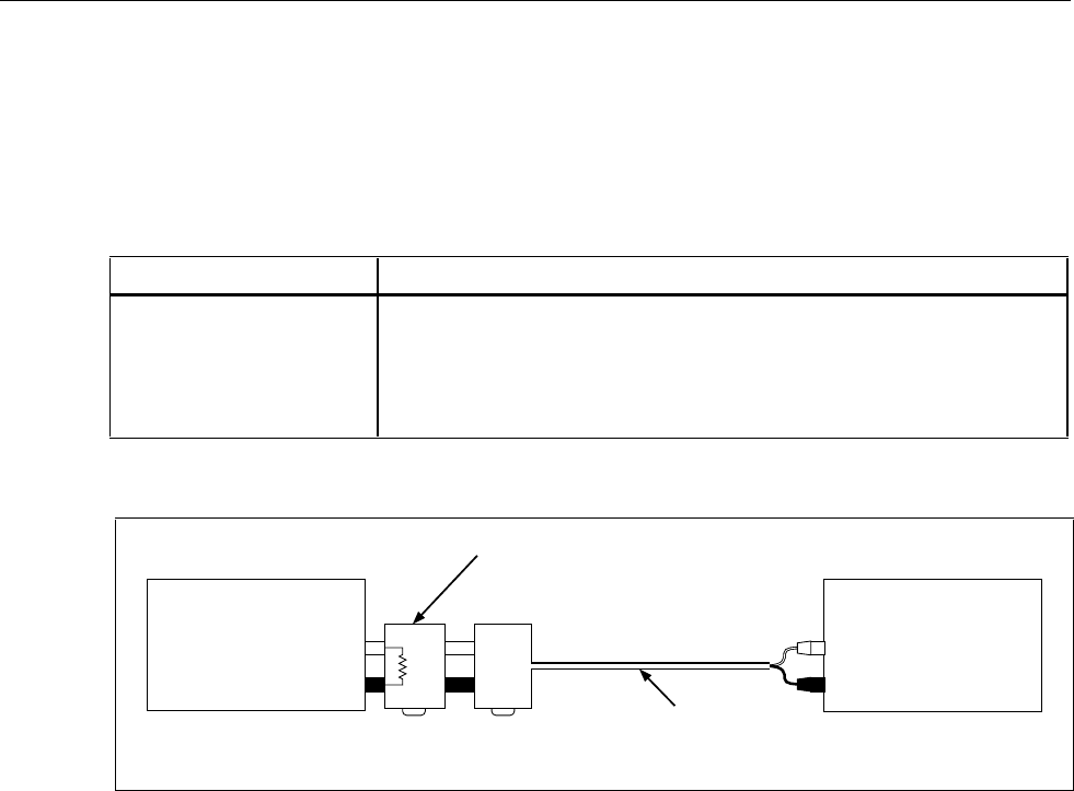
5700A/5720A Series II Calibrator
Service Manual
3-36
3-24. AC Current Test, 2 mA and 200
µ
A Ranges
The equipment required for the alternating current accuracy verification test for the 2
mA and 200 µA ranges is listed in Table 3-10. Use Table 3-28 (5720A) or 3-29 (5700A0
for the test record.
Table 3-10. Equipment Required for Alternating Current Accuracy Test for the 2 mA and 200 µA
Ranges
Equipment Model or Description
AC Measurement Standard Fluke 5790A
Metal Film Resistor 200Ω, 1/8w, ±1%, T9 (P/N 309724) mounted on a dual banana plug.
Metal Film Resistor 2 kΩ, 1/8w, ±1%, T9 (PN 335422) mounted on a dual banana plug
Cable Pomona 1368-A-18. Double banana to single banana plugs.
1. Connect the equipment as shown in Figure 3-13.
Hi
Calibrator (UUT)
Output
Pomona Cable
1362-A-18
Lo
Metal Film Resistor
Mounted on Dual
Banana Plug
5790A
Input 2
Hi
Lo
200
Ω
F3-9.EPS
Figure 3-13. Alternating Current Test Setup 2 mA and 200 µA
Note
An explanation of the rationale for using metal film resistors to measure
ac current follows this procedure.
2. Set the Calibrator for precisely +2 mA dc using the correction from previously
recorded data, i.e. set the Calibrator error display to the value recorded for +2 mA dc
(Table 3-9 or 3-11).
3. When the 5790A settles on a reading, push the SET REF soft key on the 5790A.
4. Set the Calibrator for precisely -2 mA dc output using the correction from previously
recorded data, i.e., set the Calibrator error display to the value recorded for -2 mA
dc, in Table 3-10.
5. Press the AVG REF soft key on the 5790A after the 5790A reading settles.
6. Set the Calibrator to 2 mA at 10 Hz and OPERATE.
7. Record the error displayed on the 5790A in Table 3-28 or 3-29, and verify results are
within spec.
8. Return to the error corrected +2 mA DC output that was set in step 2. Verify that the
5790A display returns to a zero reading ±10 PPM. If necessary, repeat steps 2
through 6 until the required results are obtained.
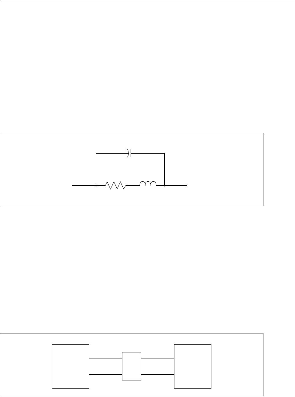
Calibration and Verification
Full Verification
3
3-37
9. Change the Calibrator frequency to 20 Hz, 40 Hz, 1 kHz, 5 kHz and 10 kHz. At each
frequency record the error display on the 5790A in Table 3-28 or 3-29. Verify that
the results are within limits shown.
10. Repeat steps 2 through 9, but replace the 200Ω metal film resistor with the 2 kΩ
resistor, and use 200 µA instead of 2 mA.
3-25. Rationale for Using Metal-Film Resistors to Measure AC Current
To be able to measure alternating current, a system comprised of a suitable ac shunt and
ac detector is required. First let us consider the ac shunt. For this example we will use a 2
kΩ metal film resistor. At frequencies up to 10 kHz, the equivalent circuit of the resistor
can be illustrated as in Figure 3-14. Values typical for shunt capacitance and series
inductance are 2 pF (Cs) and 0.01 µH (Ls). For comparison, wire has approximately 0.02
µH/inch. At 10 kHz, the reactance of Cshunt is 8 MΩ, and the reactance of Lseries is 0.6
mΩ. The formulae to use are:
SHUNT
C
SERIES
L
R
F3-10.EPS
Figure 3-14. Metal Film Resistor Equivalent Circuit
(1/Z)2 = (1/R)2 + (1/XC)2 (1)
(Z)2 = (R)2 + (XL)2 (2)
Where R = resistance Xc = Capacitive Reactance
Z = network impedance XL = Inductive Reactance
We can see that these effects can be ignored, because their contribution to errors in the
measurement process is less than 1 ppm. That is, the metal film resistor’s self reactance
is totally dwarfed by the reactance of the measuring circuit, which is overwhelmingly
capacitive.
If a detector as shown in Figure 3-15 has an input impedance of 10 MΩ shunted by 123
pF, then the effects of Xc must be accounted for. We can ignore the net resistance
change introduced by the 10 MΩ detector resistance.
SHUNT
R
DET.UUT
F3-11.EPS
Figure 3-15. Metal Film Resistor in Test Circuit

5700A/5720A Series II Calibrator
Service Manual
3-38
Note
The input impedance at INPUT 2 of the 5790A on the millivolt ranges is 10
M
Ω
shunted by 83 pF and the cable used to connect the shunt resistor to
the 5790A has 40 pF capacitance, for a total of 123 pF.
The reactance of 123 pF at 10 kHz is 129 kΩ, and using formula (1), in the case where
R=2 kΩ, the network impedance Z = 1.999760 kΩ. This produces an error of 120 PPM.
The allowable error at 10 kHz is reduced to account for this error.
Using formula (2) we get a result of Xc = 88 kΩ, and a network impedance of Z =
1.9995 kΩ. This produces an error of approximately 250 ppm, or 0.025%. However, if
we are making a measurement of 0.21% uncertainty (as in the present case), the ratio of
measurement uncertainty is about 10:1 and is not of concern. It is easy to improve
measurement uncertainty if desired, though, by measuring the actual input capacitance of
the detector and any stray capacitance from input leads, etc. and making corrections. In
this discussion, the UUT is assumed to be a high-impedance current source (like the
5700A), which can easily be verified by the manufacturer’s specifications, i.e., a
specified voltage adder for current outputs above a given burden voltage.
3-26. Wideband Frequency Accuracy Test
Use Table 3-30 for the test record. Proceed as follows to test the Wideband module
frequency accuracy:
1. Connect the Philips PM 6669 to the Calibrator wideband output and measure the
output frequency at the frequencies listed in Table 3-30.
2. Verify that the frequency counter indicates frequencies within the 0.01% limits
shown.
3-27. Wideband AC Voltage Module Output Verification
The wideband tests are for units with the Option 5700A-03 Wideband AC Module only.
The verification test for the wideband module works as follows:
• Accuracy at 1 kHz: Output at 1 kHz is tested by comparing the wideband output at
the end of the cable and termination supplied with the instrument to the 5790A at
INPUT 2.
• Attenuator flatness: The attenuator flatness is tested using the 5790A wideband input
and using reduced spec limits when the TUR (Test Uncertainty Ratio) is less than
4:1.
Table 3-11 lists the equipment required for testing and calibrating the Wideband module.
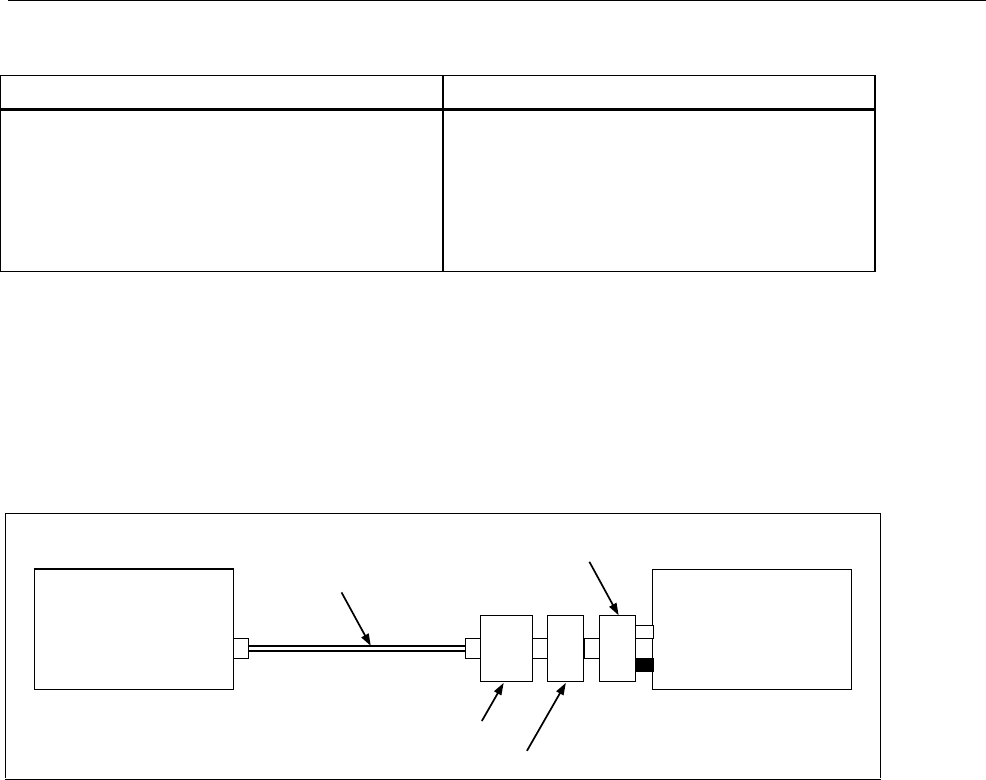
Calibration and Verification
Wideband Output Accuracy at 1 kHz Test
3
3-39
Table 3-11. Equipment Required for Testing and Calibrating the Wideband Option
Equipment Model or Description
AC Measurement Standard Fluke 5790A with Wideband Option -03
Wideband cable Supplied with 5700A-03
50Ω Termination Supplied with 5700A-03
Adapter Pomona 1269 BNC(F) to dual banana plug.
Adapter Kings KN-99-46 N(F) to BNC(M)
3-28. Wideband Output Accuracy at 1 kHz Test
This test verifies the Wideband output level at 1 kHz by direct measurement with the
5790A at INPUT 2. Use Table 3-31 for a test record.
Proceed as follows to characterize the rms wideband voltmeter at 1 kHz:
1. Connect the equipment as shown in Figure 3-16.
Input 2
Calibrator (UUT)
Wideband
Output
N(F) to BNC(M) Adapter
BNC(F) to Banana Adapter
5790A
50Ω Termination
Wideband
Output Cable
F3-12.EPS
Figure 3-16. Wideband Accuracy at 1 kHz Test Setup
2. Set the Calibrator wideband output to 2.1V at 1 kHz and the 5790A to read INPUT
2.
3. Push the 2.2V RANGE button on the 5790A to lock it on the 2.2V range.
4. On the 5790A push UTIL MENUS button and then MEAS CONTROL soft key. Set
the digital filter mode to FAST and the restart to MEDIUM. Push the DONE soft
key twice to return to the measurement display.
5. Use the Calibrator output adjustment knob to obtain a reading on the 5790A
measurement display of 2.100000 ±20 counts.
6. Read the error on the Calibrator display and record it in Table 3-32 for the 2.1V
level for the appropriate verification internal. Verify that it is within spec limits
shown.
7. Push the soft key under the RANGE display on the 5790A to return to AUTO
RANGE.
8. Proceed to the remaining levels shown in Table 3-32 and repeat steps 5 through 7
with the appropriate output levels set in each step, using the adjustment tolerance in
Table 3-12 in step 5.
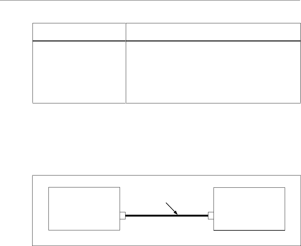
5700A/5720A Series II Calibrator
Service Manual
3-40
Table 3-12. Wideband Adjustment Tolerance
5700A/5720A Series II Wideband
Output
5790A Adjustment Counts
± ppm
2.10000V 20
1.00000V 10
300.000 mV 3
100.000 mV 10
30.0000 mV 3
10.0000 mV 1
3.00000 mV 1
1000.00 µV1
3-29. Wideband Output Flatness Test
Use Table 3-32 as a test record. To perform wideband output flatness test, proceed as
follows:
1. Connect the equipment as shown in Figure 3-17. Note that the Calibrator wideband
cable is connected to the 5790A directly, the termination is not used.
5790A
Wideband
Input
Calibrator (UUT)
Wideband
Output
Wideband
Output Cable
F3-13.EPS
Figure 3-17. Wideband Flatness Test Setup
2. Set the wideband output to 3V at 1 kHz.
3. Push the WBND button on the 5790A, when the reading has settled, push the SET
REF soft key.
4. Set the Calibrator to frequencies shown in Table 3-32 for the 3V output and record
the errors on the 5790A error display at each frequency in Table 3-32.
5. Verify that the error readings are within spec limits or reduced spec limits shown on
the test record. Reduced spec limits are used when the TUR (Test Uncertainty Ratio)
is less than 4:1.
6. Repeat steps 4 and 5 for the remaining output levels shown in Table 3-32 using the
appropriate voltage in step 4.
7. Record the 1 kHz absolute errors at each output level from Table 3-32 into the
appropriate column in Table 3-33. Record the flatness errors from Table 3-32 for
each output level and frequency into the appropriate column in Table 3-33. Add the
errors and verify that they are within spec for the appropriate time internal.

Calibration and Verification
Wideband Output Flatness Test
3
3-41
3-30. Wideband Flatness Calibration Procedure
This procedure is the only part of full verification that stores calibration constants in the
Calibrator. This is not a verification test, it is a calibration procedure. Because this part
of calibration is recommended to be done only every two years, the same interval as full
verification, it is included here and not under Calibration earlier in this chapter and in
Chapter 7 of the 5700A/5720A Series II Operator Manual.
Proceed as follows to perform wideband flatness calibration:
1. Connect the equipment as shown in Figure 3-12 and set the rear panel
CALIBRATION switch to the ENABLE position.
2. Push the WBND button on the 5790A.
3. Call up the wideband flatness calibration routine on the Calibrator front panel, by
pressing the softkey sequence SETUP MENUS, CAL, CALIBRATION and
WIDEBAND FLAT.
4. Enter the present ambient air temperature as prompted and press ENTER.
5. Place the Calibrator in OPERATE. Wideband flatness calibration starts with a 3V
output at 1 kHz.
6. Push the SET REF soft key on the 5790A when the 5790A settles to a reading. This
is the 3V reference value from which all other frequencies will be compared.
7. Push the ENTER button on the Calibrator, and, the frequency will advance to the
next value.
8. Adjust the Calibrator output adjustment knob to bring the 5790A error display to 0
and press ENTER on the Calibrator. Repeat this step for each frequency through 30
MHz.
9. Push the CLEAR REF WBND soft key on the 5790A. The Calibrator wideband
output changes to 1V at 1 kHz.
10. Push the SET REF soft key on the 5790A when the 5790A settles to a reading,. This
is the 1V reference value from which all other frequencies will be compared.
11. Repeat steps 7 and 8 above for each frequency through 30 MHz.
12. Push the CLEAR REF WBND soft key on the 5790A. The Calibrator Wideband
output changes to 300 mV at 1 kHz.
13. Push the SET REF soft key on the 5790A when the 5790A settles to a reading. This
is the 300 mV reference value from which all other frequencies will be compared.
14. Repeat steps 7 and 8 above for each frequency through 30 MHz.
15. Push the CLEAR REF WBND soft key on the 5790A. The 5790A wideband output
changes to 100 mV at 1 kHz.
16. Push the SET REF soft key on the 5790A when the 5790A settles to a reading. This
is the 100 mV reference value from which all other frequencies will be compared.
17. Repeat steps 7 and 8 above for each frequency through 30 MHz. Only the 10 MHz,
20 MHz and 30 MHz points are adjusted.
18. Push the CLEAR REF WBND soft key on the 5790A. The 5790A wideband output
changes to 30 mV at 1 kHz.
19. Push the SET REF soft key on the 5790A when the 5790A settles to a reading. This
is the 30 mV reference value from which all other frequencies will be compared.
20. Repeat steps 7 and 8 above for each frequency through 30 MHz.

5700A/5720A Series II Calibrator
Service Manual
3-42
21. Push the CLEAR REF WBND soft key on the 5790A. The 5790A wideband output
changes to 10 mV at 1 kHz.
22. Push the SET REF soft key on the 5790A when the 5790A settles to a reading. This
is the 10 mV reference value from which all other frequencies will be compared.
23. Repeat steps 7 and 8 above for each frequency through 30 MHz. Only the 10 MHz,
20 MHz and 30 MHz points are adjusted.
24. Make sure the rear panel CALIBRATION switch is in the ENABLE position. Store
the cal constants by pushing the STORE VALUES softkey. When the display returns
to normal, set the rear panel CALIBRATION switch to NORMAL. The Calibrator
wideband flatness calibration is now complete.
3-31. Optional Tests
These tests may be used in acceptance testing or following repair likely to affect the
characteristics tested here. They are not recommended to be done routinely. If the
Calibrator passes Calibration Performance Verification, you do not need to perform
these tests; verification either exercises these functions or is subject to their effects. The
Optional Tests include such checks as load regulation, noise, and distortion. Equipment
required for the optional tests is listed in Table 3-13.
Table 3-13. Equipment Required For DC V Optional Tests
Equipment Model
DMM Wavetek 1281 or HP 3458A
RMS Differential Voltmeter Fluke 5790A
Power Decade Resistor Clarostat 240C
Differential Amplifier Plug-In Tektronix 7A22
Oscilloscope Mainframe Tektronix 7000 Series
DC Voltage Reference Standard Fluke 732B
Reference Divider Fluke 752A
Null Detector EM Electronics N11(Fluke 845A)
Kelvin-Varley Divider Fluke 720A
3-32. DC Voltage Load Regulation Test
Use Table 3-34 for a test record. Proceed as follows to test the dc voltage load
regulation:
1. Ensure the Calibrator is in standby. With the test setup of Figure 3-5, connect the
power decade resistor across the Calibrator OUTPUT terminals. Connect two
shorting links between the Calibrator SENSE and OUTPUT terminals and select
external sense (EX SNS indicator lit).
2. Set the reference divider to 10V. Set the Calibrator output to 10V dc. Set the power
decade resistor to 199Ω. Set the Calibrator to operate. Adjust the Calibrator as
necessary to obtain a null on the null detector. Rotate the most significant dial on the
power decade resistor to 9. Verify that the null detector indication changes less than
±2 µV. Set the Calibrator to standby.
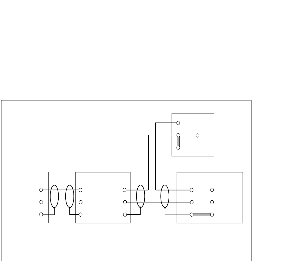
Calibration and Verification
Optional Tests
3
3-43
3. Repeat load regulation testing at the remaining Calibrator outputs shown in Table
3-47.
4. Set the Calibrator to standby and disconnect all equipment from the Calibrator.
3-33. DC Voltage Linearity Test
Use Table 3-35 for a test record. Proceed as follows to test the dc voltage linearity:
1. Self calibrate the Kelvin-Varley (KV) divider as called for in its service manual.
2. Connect the equipment as shown in Figure 3-18.
10V
732B
HI
NULL DETECTOR
LO
INPUT OUTPUT
HI
720A
HI
LO
GND GND
LO
OUTPUT SENSE
HI
CALIBRATOR (UUT)
HI
LO
GRD GND
LO
GRD
HI
LO
GRD
*NOTE:
IF THE NULL DETECTOR IS NOT GROUNDED THROUGH
POWER LINE, CONNECT ITS GROUND TERMINAL
TO THE GROUND TERMINAL ONTHE 5700A.
GND*
F3-14.EPS
Figure 3-18. DC Voltage Linearity Test
3. Set the KV dials to zero by using the RANGE LOCK. Set the Calibrator to 0V on the
11V range operate. Note the null detector reading. Press OFFSET on the Calibrator.
4. Set KV dials to 0.999999X and Calibrator for a 10V output.
5. Use the Calibrator output adjustment to obtain a null detector reading equal to the
reading noted in step 3. Press SCALE on the Calibrator.
6. For each of the KV settings tabulated in Table 3-36, make the required Kelvin
Varley setting, and verify that the null detector reads within the limits shown.
3-34. DC Voltage Output Noise
(
10 Hz to 10 kHz
)
Test
Use Table 3-36 for a test record. Proceed as follows to test the dc voltage output noise
that falls in the range 10 Hz to 10 kHz:
1. Connect the equipment as shown in Figure 3-19.
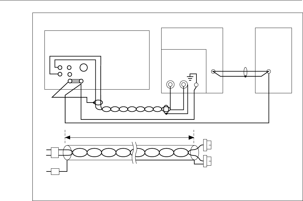
5700A/5720A Series II Calibrator
Service Manual
3-44
LO
OUTPUT
SENSE
HI
CALIBRATOR
(UUT)
GRD GND
SHIELDED
TWISTED PAIR
OUTPUT
COAX
TRUE RMS
VOLTMETER
VERTICAL
OSCILLOSCOPE
MAINFRAME*
7A22
PLUG-IN
CLIP LEADS
3' APPROX
GR BANANA PLUGS
SHIELDED TWISTED PAIR CABLE DETAIL
BNC
OSCILLOSCOPE AND AC DIFFERENTIAL
VOLTMETER SHOULD BE ISOLATED FROM
THE POWER LINE GROUND.
*
F3-15.EPS
Figure 3-19. DC Voltage Output Noise Test Setup
2. Set the Oscilloscope Differential Amplifier controls as shown below.
Low Frequency -3 dB
High Frequency -3 dB
Input Coupling
Volts/Div
10 Hz
10 kHz
AC (both inputs)
50 µV (Var. to Cal.)
3. Set the Oscilloscope Time/Div for 2 ms.
4. Set the rms voltmeter range to 1V.
5. Set the Calibrator to 2.2V dc, operate. Verify that the reading on the rms voltmeter is
less than 150 mV.
NOTE
This test assumes that the amplifier plug-in and scope have a gain equal
to 0.5V divided by the input/div. setting, which in the above case is 1x10⁴.
6. Repeat the above process for the remaining tabulated settings shown in Table
3-49; verify that the rms meter indicates less than the amount shown for each
required output level.
7. Press RESET on the Calibrator and disconnect the test configuration.

Calibration and Verification
Optional Tests
3
3-45
3-35. DC Voltage Output Noise
(
0
.
1 to 10 Hz
)
Test
Proceed as follows to test for dc voltage output noise in the range 0.1 to 10 Hz:
1. Place the 8520A DMM into Math Program 8 with the Display Option Register set to
register 8.3 (Standard Deviation Computed Variable)as follows:
a. Press SHIFT, 8, and PROGRAM SELECTION. Then press SHIFT, 0, ., 1,
PROGRAM SELECTION, 8, ., 3, PROGRAM DATA.
b. Set the DMM to 200 mV DC Range, 20 Samples/Second, and 1000 ms Filter.
c. Set PROGRAMS IN USE to the ON position.
2. Lock the Calibrator in the 22V range and set it to 100 mV dc. Place the Calibrator in
operate.
3. Connect the DMM to the Calibrator OUTPUT binding posts and press the DMM
reset button once. Verify that after 10 seconds the DMM reads less than 0.0010E-3.
4. Lock the Calibrator in the 220V range and set it to 100 mV dc. Place the Calibrator
in operate.
5. Press the DMM reset button once. Verify that after 10 seconds the DMM reads less
than 0.0100E-3.
6. Set the Calibrator to standby.
3-36. AC Voltage Distortion Test
Equipment required for these tests is listed in Table 3-14. Proceed as follows to test for
distortion in the ac voltage function. Use Table 3-37 for test record.
Table 3-14. Equipment Required for Distortion Test
Equipment Model
DMM Wavetek 1281 or HP 3458A
Distortion Analyzer Krohn-Hite 6900B
Spectrum Analyzer (only for 5700A-03) HP 8590A
Non-wirewound load resistors Any (see *Table 3-50 for values)
1. Connect the Calibrator output terminals to the distortion analyzer.
2. Measure the Calibrator distortion at the output voltages and frequencies tabulated in
Table 3-37. Verify that the distortion measured is within the limits shown.
WWarning
A non-reactive voltage divider may be necessary to scale the
test voltages to match the distortion analyzer characteristics.
3-37. Wideband Distortion Testing
Proceed as follows to test for distortion in the wideband output function (for units with
the Option 5700A-03 Wideband AC Module only).
1. Connect the Wideband output terminated in 50Ω to the spectrum analyzer input.

5700A/5720A Series II Calibrator
Service Manual
3-46
Note
If the spectrum analyzer input impedance is 50
Ω
, do not use a separate
termination.
2. With 0 dBm output programmed from the Calibrator wideband output, select
frequencies over the band of 1 MHz to 30 MHz and verify that use the spectrum
analyzer to verify that any harmonics are below -40 dBm for fundamentals up to 10
MHz and below -34 dBm for fundamentals of 10 MHz and above.
3. Disconnect the equipment from the Calibrator.
3-38. AC Voltage Overshoot Test
Proceed as follows to test for ac voltage overshoot:
1. Connect the Calibrator output to a properly compensated 10:1 probe.
2. AC couple the oscilloscope and set the sweeptime to a fairly low sweeptime
(approximately 1 sec/div).
3. Set the Calibrator to 7.07V at 1 kHz, and press OPR/STBY.
4. Set the scope vertical sensitivity for 0.05V/div. Offset the trace vertically until you
can see the top of the waveform at the approximate center of the display (must be at
least 2-3 divisions down from the top of the scope graticule).
5. Set the Calibrator to standby and then back to operate. Verify that any overshoot
visible on the oscilloscope display is less than 1.5 divisions (approximately 10% of
the peak value).
6. Repeat the test at 100 Hz and 100 kHz. This completes the Optional Tests.
3-39. Minimum Use Requirements
Table 3-15 defines specifications for test equipment needed for tests in this section of the
manual. If the specific test equipment called for in these tests is not available, you can
substitute equipment that meets these specifications.

Calibration and Verification
Minimum Use Requirements
3
3-47
Table 3-15. Minimum Use Requirements
Item
No. Description Minimum Use Specifications Recommended
Equipment
Calibration Equipment
1. Voltage Reference 10V nominal, true value certified to within
±1.5 ppm
Fluke 732B
2. Resistance Standards 1Ω nominal, true value certified to within 10
ppm, 10 kΩ nominal, true value certified to
within 4 ppm
Fluke 742A Series, 1Ω
and 10 kΩ
Calibration Verification Equipment
3. Reference Voltage
Divider Range uncertainty 100:1, 1 kV input, ±0.5
ppm 10:1 100V input ±0.2 ppm
Fluke 752A
4. Null Detector Leakage resistance to case: 1012Ω min.
Resolution: 3 µV full scale
EM Electronics N11
(Fluke 845A)
5. Low Thermal EMF
Cables Plug-in. Copper or gold-flashed copper (two
cables per set, two sets required).
Fluke 5440A-7002
Spade lug. Copper or gold-flashed copper
(two cables per set, two sets required).
Fluke 5440A-7003
6. Digital Multimeter DC Voltage Range: 0.1 to 10V Resolution
and short-term stability: ±2 ppm Resistance
range: 1Ω to 10 MΩ Resolution and short-
term stability :±20 uΩ at 1Ω, 1.9Ω ±5 ppm at
10Ω, 19Ω ±2 ppm at 100Ω to 1.9 MΩ ±4
ppm at 10 MΩ, 19 MΩ
Wavetek 1281 or
HP 3458A
7. Current Source Range: 10 mA and 100 mA Typical short-
term stability ±15 ppm for 5 minutes
Fluke 55X0A,
5700A/5720A Series II,
8. AC Measurement
Standard Ranges: 2.2 mV through 1000V AC
Frequency: 10 Hz to 1 MHz
24 to 7500 ppm, depending on amplitude
and frequency (see Table 3-9.)
Wideband Ranges: 2.2 mV through 7V
Frequency: 10 Hz to 30 MHz
Uncertainty: 0.03% to 0.9%, depending on
amplitude and frequency (see Table 3-18.)
Fluke 5790A (Option -
03 required for
Wideband Flatness
Verification)

5700A/5720A Series II Calibrator
Service Manual
3-48
Table 3-15. Minimum Use Requirements (cont)
Item
No. Description Minimum Use Specifications Recommended
Equipment
9. Current Shunt Adapter Used in conjunction with 5790A and A40-
series shunts to facilitate AC Current
measurements
Fluke 792A-7004
10. Frequency Counter 10 Hz to 30 MHz ±0.002% Philips PM 6669
11. Standard Resistors (1) 0.1Ω nominal, true value certified to within
20 ppm, rated for 2A DC; 1Ω nominal, true
value certified to within 6 ppm; 1.9Ω
nominal, true value certified to within 6 ppm;
10Ω nominal, true value certified to within 6
ppm; 1 kΩ nominal, true value certified to
within 5.5 ppm; 10 kΩ nominal, true value
certified to within 3.5 ppm; 19 kΩ nominal,
true value certified to within 4 ppm; 10 MΩ
nominal, true value certified to within 15
ppm; 19 MΩ nominal, true value certified to
within 28 ppm
Fluke 742A-1
Fluke 742A-1.9
Fluke 742A-10
Fluke 742A-1k
Fluke 742A-10k
Fluke 742A-19k
Fluke 742A-10M
Fluke 742A-19M
L&N 4221B (0.1Ω)
12. DC Current Shunt (2) Range: 10A
Uncertainty: ±0.008%
Fluke Y5020
13. AC/DC Current Shunt Ranges: 20 mA, 200 mA, 2A and 10A
Frequency: 10 Hz to 10 kHz
Uncertainty: ±310 ppm at 10 Hz; ±100 ppm
at 20 Hz; ±50 ppm at 40 Hz, 1 kHz; ±100
ppm at 5 kHz, 10 kHz
Fluke A40-20 mA
Fluke A40-200 mA
Fluke A40-2A
Fluke A40A-10A (2)
14. Metal Film Resistors Values: 200Ω, 2 kΩ, and 1 MΩ Temperature
C°: T9 or better Power Rating: 1/4 Watt
Tolerance: ±1%
Stock Items
15. Differential Amplifier Sensitivity: 5 µV rms Bandwidth selectable
to 10 kHz Tektronix 7A22 w/7000-
Series Mainframe
16. Distortion Analyzer Range: 2V to 300V
Frequency: 10 Hz to 600 kHz
Krohn-Hite 6900B
17. Kelvin-Varley Voltage
Divider Ratio uncertainty: ±0.1 ppm of input Fluke 720A
18. HF Spectrum Analyzer
(used in optional test
for wideband
distortion)
Freq. Range: 2 MHz to 120 MHz Input
Level: 3V (+20 dBm to -60 dBm) HP 8590A
1: A DMM may be used for all but the 1
Ω
and 1.9
Ω
values. For those values using the DMM, a test method
using an external current source is used for low-value resistance.
2: Needed only for 5725A Amplifier testing.
3-40. Determining Test Limits for Other Calibration Intervals
The verification procedures in this chapter test to the 90 day 99% confidence
specification limits. For other calibration intervals it is necessary to calculate new
specification limits and, if necessary, new test limits.
The following examples show how the 90 day limits were calculated. These examples
illustrate how you can calculate the specifications and test limits, if necessary, for other
calibration intervals.
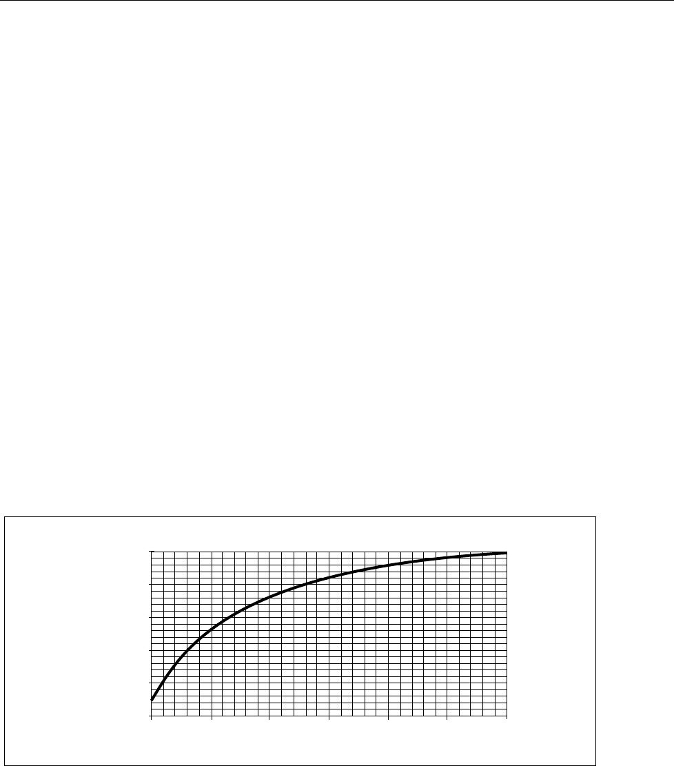
Calibration and Verification
Determining Test Limits for Other Calibration Intervals
3
3-49
Example 1 shows you how to calculate a specification limit for a specific test level from
a specification listed as a percentage (or parts per million) of reading plus a floor error in
microvolts, millivolts, miroamps, or nanoamps.
The 99% confidence specification for a 5720A at 2 mA, 1 kHz is 130 ppm + 40 nA. We
can convert the floor uncertainty of 40 nA to ppm of output by dividing 40 nA by 2 mA
and multiplying by a million:
(130 + 1000000*0.000000040/0.002)=130 ppm + 20 ppm = 150 ppm
This test limit is shown in Table 3-28.
If we wanted to test to the 1 year specification of 140 ppm + 40 nA, the test limit would
be the specification of 140 ppm + 40 nA = 140 ppm + 40 ppm = 180 ppm.
Example 2 shows you how to calculate a specification limit and a tighter test limit. For
instrumentation that have the precision of the 5720A/5700A Series II calibrators, it is
difficult obtain standards which are many times more accurate than the calibrator
specifications. Therefore, for cases when the test uncertainty ratio (TUR) of the
standards is less than 4:1, guardbanding is used to set test limits which are tighter than
the specification limits. These limits provide the same risk of accepting out of tolerance
instruments as a TUR of 4:1. The statistical analysis of the guardbanding techniques
used are described in a series of technical papers referenced at the end of this chapter.
Guardbanding is used to set the test limits different than the specification limits for a
5720A at 2V, 1 kHz. The 90 day specification is 47 ppm + 10 uV. When you calculate
the specification in ppm at the 2V level in the same way as in Example 1, the
specification limit is:
(47 + 1000000*0.000010/2)=47 ppm + 5 ppm = 52 ppm.
99% Confidence Guardband Factors
0.750
0.800
0.850
0.900
0.950
1.000
1.00 1.50 2.00 2.50 3.00 3.50 4.00
Test Uncertainty Ratio
Guardband Factor (K)
CHART.EPS
Figure 3-20. Determining Other Test Limits

Table 3-16. 5720A Resistance Test Record
1Ω Std Res
Value 1Ω Std
Voltage Measured
1Ω Std
Voltage
Cal
Current UUT 1Ω
Displayed
Value
UUT 1Ω
Voltage UUT
True
Res
UUT
Dev. Uncert
Std Spec
(±ppm) TUR GB
Factor Test
Limit
(±ppm)
Max
Difference of
Charactized to
Nominal Value
5.9 95 16.06 1.000 95 0.9995 to 1.0005
1.9Ω Std
Res Value 1.9Ω Std
Voltage Measured
1.9Ω Std
Voltage
Cal
Current UUT
1.9Ω
Displayed
Value
UUT
1.9Ω
Voltage
UUT
True
Res
UUT
Dev. Spec
(±ppm) Max
Difference of
Characterized to
Nominal Value
5.9 95 16.06 1.000 95 1.89905 to
1.90095
10Ω Std
Res Value 10Ω Std
Voltage Measured
10Ω Std
Voltage
Cal
Current UUT 10Ω
Displayed
Value
UUT
10Ω
Voltage
UUT
True
Res
UUT
Dev. Spec
(±ppm) Max
Difference of
Characterized to
Nominal Value
5.9 25 4.23 1.000 25 9.997 to 10.004
Resistance Accuracy Verification (19Ω And Above)
Std
Res
Value
DMM Std
Res Rdg DMM
Error DMM
UUT Res
Value
UUT True
Res Value UUT Dev. Uncert
Std Spec
(±ppm) TUR GB
Factor Test
Limit
(±ppm)
Max
Difference of
Characterized to
Nominal Value
19Ω (1) 25 18.9943 to 19.0057
100Ω (1) 5.1 11 2.16 0.970 10.7 99.985 to 100.015
190Ω (1) 11 189.9715 to 190.0285
1 kΩ (1) 4.7 9 1.91 0.926 8.3 999.85 to 1000.15
1.9 kΩ (1) 9 1.899715k to 1.900285k
10 kΩ3.1 9 2.92 0.978 8.8 9.9985k to 10.0015k
19 kΩ3.5 9 2.55 0.963 8.7 18.99715k to 19.00285k
100 kΩ(1) 5.1 11 2.15 0.942 10.4 99.985k to 100.015k
190 kΩ (1) 11 189.9715k to 190.0285k
1 MΩ (1) 8.1 18 2.23 0.948 17.1 0.9998M to 1.0002M

3-51
Table 3-16. 5720A Resistance Test Record (cont)
Std
Res
Value
DMM Std
Res Rdg DMM
Error DMM
UUT Res
Value
UUT True
Res Value UUT Dev. Uncert
Std Spec
(ppm) TUR GB
Factor Test
Limit
(±ppm)
Max
Difference of
Characterized to
Nominal Value
1.9 MΩ (1) 19 1.89962M to 1.90038M
10 MΩ)12.0 37 3.07 0.982 36.3 9.997M to 10.003M
19 MΩ21.9 47 2.15 0.942 44.3 18.9943M to 19.0057M
100 MΩ
(2)
110 99.95M to 100.05M
1: Not necessary to test due to 5720A Series II internal calibration process. Uncertainties and test limits are shown for other available 742A Standard Resistors.
2: Due to extremely slow settling time (approximately 5 minutes to 0.005% and sensitivity to any nearby movement, use of the DMM to test 100 megohms to the
specified 0.01% uncertainty is not practical and therefore is not recommended. For those who wish to test it, a suitable way is to use an ESI SR 1050 10M/step
Hamon-type Resistance Transfer Standard and use it in conjunction with an ESI 242-series bridge to effect the measurement to the required uncertainty.

Table 3-17. 5700A Resistance Test Record
1Ω Std Res
Value 1Ω Std
Voltage
Measured
1Ω Std
Voltage
Cal
Current
UUT 1Ω
Displayed
Value
UUT 1Ω
Voltage UUT
True
Res
UUT
Dev. Uncert
Std Spec
(ppm) TUR GB
Factor Test
Limit
(ppm)
Max
Difference of
Characterized to
Nominal Value
5.9 95 16.06 1.000 95 0.9995 to 1.0005
1.9Ω Std
Res Value 1.9Ω Std
Voltage
Measured
1.9Ω Std
Voltage
Cal
Current
UUT
1.9Ω
Displayed
Value
UUT
1.9Ω
Voltage
UUT
True
Res
UUT
Dev.
Spec
(ppm) TUR GB
Factor Test
Limit
(ppm)
Max
Difference of
Characterized to
Nominal Value
5.9 95 16.06 1.000 95 1.89905 to 1.90095
10Ω Std
Res Value 10Ω Std
Voltage
Measured
10Ω Std
Voltage
Cal
Current
UUT 10Ω
Displayed
Value
UUT
10Ω
Voltage
UUT
True
Res
UUT
Dev.
Spec
(ppm) TUR GB
Factor Test
Limit
(ppm)
Max
Difference of
Characterized to
Nominal Value
5.9 28 4.73 1.000 28 9.997 to 10.004
Resistance Accuracy Verification (19Ω And Above)
Std
Res
Value
DMM Std
Res Rdg DMM
Error DMM
UUT Res
Value
UUT True
Res Value UUT Dev. Uncert.
std Spec
(±ppm) TUR GB
Factor Test
Limit
(±ppm)
Max
Difference of
Characterized to
Nominal Value
19Ω (1) 18.9943 to 19.0057
100Ω (1) 5.1 17 3.33 0.990 16.8 99.985 to 100.015
190Ω (1) 11 189.9715 to 190.0285
1 kΩ (1) 4.7 12 2.54 0.963 11.6 999.85 to 1000.15
1.9 kΩ (1) 9 1.899715k to 1.900285k
10 kΩ3.1 11 3.57 0.994 10.9 9.9985k to 10.0015k
19 kΩ3.5 11 3.11 0.984 10.8 18.99715k to 19.00285k
100 kΩ(1) 5.1 13 2.54 0.963 12.5 99.985k to 100.015k
190 kΩ (1) 11 189.9715k to 190.0285k
1 MΩ (1) 8.1 18 2.23 0.948 17.1 0.9998M to 1.0002M

Table 3-17. 5700A Resistance Test Record (cont)
Std
Res
Value
DMM Std
Res Rdg DMM
Error DMM
UUT Res
Value
UUT True
Res Value UUT Dev. Uncert.
std Spec
(±ppm) TUR GB
Factor Test
Limit
(±ppm)
Max
Difference of
Characterized to
Nominal Value
1.9 MΩ (1) ±19 1.89962M to 1.90038M
10 MΩ12.0 ±37 3.07 0.982 36.3 9.997M to 10.003M
19 MΩ)21.9 ±47 2.15 0.942 44.3 18.9943M to 19.0057M
100 MΩ
(2)
±110 99.95M to 100.05M
1: Not necessary to test due to 5720A Series II internal calibration process. Uncertainties and test limits are shown for other available 742A Standard Resistors.
2: Due to extremely slow settling time (approximately 5 minutes to 0.005% and sensitivity to any nearby movement, use of the DMM to test 100 megohms to the
specified 0.01% uncertainty is not practical and therefore is not recommended. For those who wish to test it, a suitable way is to use an ESI SR 1050 10M/step
Hamon-type Resistance Transfer Standard and use it in conjunction with an ESI 242-series bridge to effect the measurement to the required uncertainty.
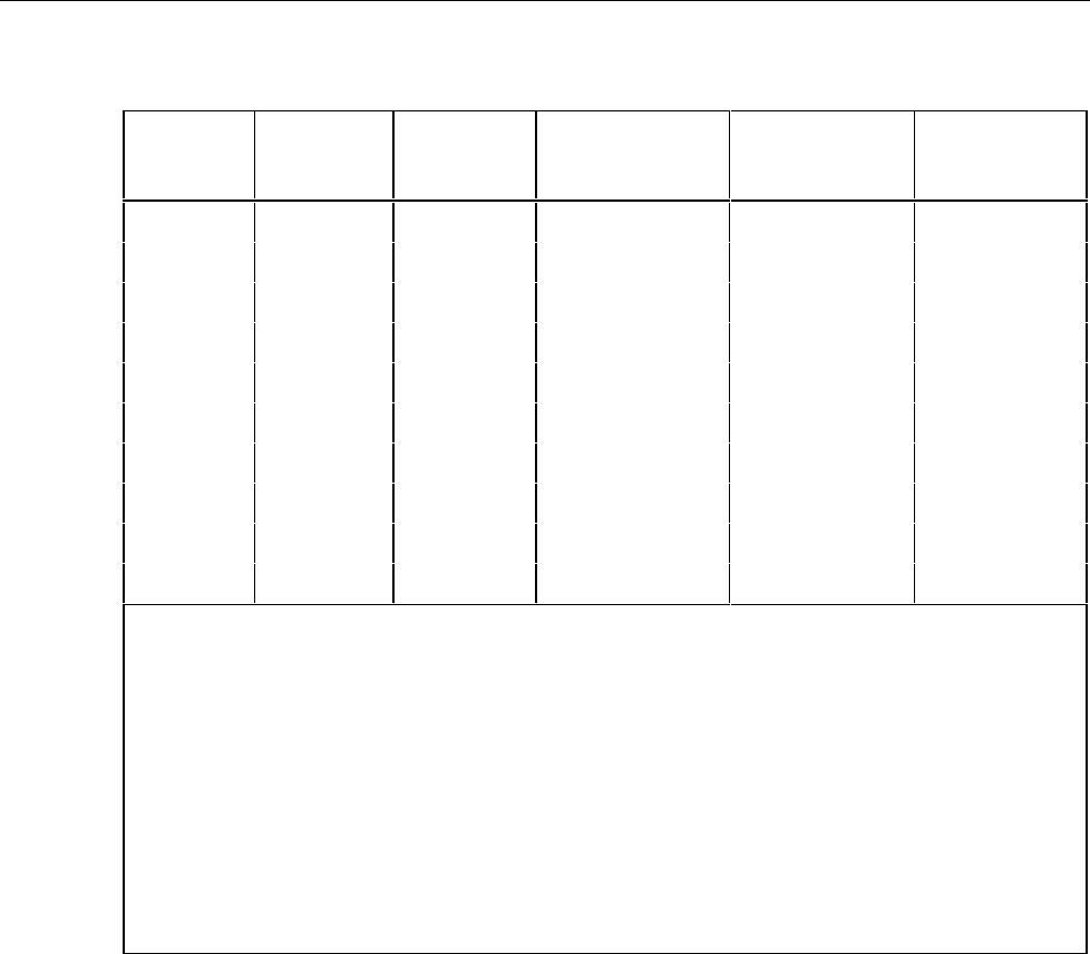
5700A/5720A Series II Calibrator
Service Manual
3-54
Table 3-18. DC Voltage Test Record for 5720A
Divider
Setting 5720A
Range
5720A
Output
(1)
Null Detector
Reading(µV)
(2)
Null Det Limit
(µV) Meter Limit
Rattle (µV)
0.1V 0.22V 0.1V ±1.20 (2) NA
1V 2.2V 1V ±4.8 µV (2) 0.55
1V 11V 1V (3) ±6 (2) 2.2
10V 11V 10V (4) ±33 3.5
10V 22V 10V (3) ±35 5.5
100V 220V 100V ±45 7.5
1000V 1100V 1000V ±65 4.5
0.1V 0.22V -0.1V ±1.20 (2) NA
1V 2.2V -1V ±4.8 (2) 0.55
10V 11V -10V ±6.0 (2) 2.2
1: Mathematically, the true 5700A/5720A Series II output programmed is the certified value of the
reference standard divided by the reference standard nominal value, multiplied by the required
5700A/5720A Series II nominal output. In other words, the 5700A/5720A Series II output is always
programmed for the nominal output adjusted up or down by the same percentage as the certified
value of the reference standard.
2: On the 752A 0.1 and 1V ranges, the null detector polarity is reversed. A low input (5700A/5720A
Series II output) causes a positive null detector reading.
3: Use Range Lock to obtain 1V on 11V and 10V on 22V range. Deactivate Range Lock before setting
the next voltage output.
4: Line regulation can be verified at this time by adjusting the autotransformer for a
±
10% change in line
voltage. The null detector reading must remain constant within
±
1
µ
V.

Calibration and Verification
Determining Test Limits for Other Calibration Intervals
3
3-55
Table 3-19. DC Voltage Test Record for 5700A
Divider
Setting 5700A
Range
5700A
Output
(1)
Null Detector
Reading(µV)
(2)
Null Det Limit
(µV) Meter Limit
Rattle (µV)
0.1V 0.22V 0.1V ±1.45 (2) NA
1V 2.2V 1V ±7.2 (2) 0.55
1V 11V 1V (3) ±9 (2) 2.2
10V 11V 10V (4) ±54 3.5
10V 22V 10V (3) ±58 5.5
100V 220V 100V ±70 7.5
1000V 1100V 1000V ±86 4.5
0.1V 0.22V -0.1V ±1.45 (2) NA
1V 2.2V -1V ±7.2 (2) 0.55
10V 11V -10V ±9.0 (2) 2.2
1: Mathematically, the true 5700A/5720A Series II output programmed is the certified value of the
reference standard divided by the reference standard nominal value, multiplied by the required
5700A/5720A Series II nominal output. In other words, the 5700A/5720A Series II output is always
programmed for the nominal output adjusted up or down by the same percentage as the certified
value of the reference standard.
2: On the 752A 0.1 and 1V ranges, the null detector polarity is reversed. A low input (5700A/5720A
Series II output) causes a positive null detector reading.
3: Use Range Lock to obtain 1V on 11V and 10V on 22V range. Deactivate Range Lock before setting
the next voltage output.
4: Line regulation can be verified at this time by adjusting the autotransformer for a
±
10% change in line
voltage. The null detector reading must remain constant within
±
1
µ
V.
5700A/5720A Series II Calibrator
Service Manual
3-56
Table 3-20. Direct Current Accuracy Test Record (5720A)
Characterizing dc DMM @ ±200 mV and ±2.0V
Output
Current
Std
Res
Value
DC DMM
Setting Rdg. Column A
Std Res
Correction
(ppm)
Column B
UUT Error
Reading
(ppm)
UUT Actual
Error (A+B)
(ppm)
Test Limit,
90-day
(±ppm)
+2A 0.1Ω(200 mV) 118
-2A 0.1Ω(200 mV) 118
+200 mA 1.0Ω(200 mV) 57
-200 mA 1.0Ω(200 mV) 57
+20 mA 10Ω(200 mV) 38
-20 mA 10Ω(200 mV) 38
+2 mA 1 kΩ(2V) 39
-2 mA 1 kΩ(2V) 39
+200 µA 10 kΩ(2V) 49
-200 µA 10 kΩ(2V) 49

Calibration and Verification
Determining Test Limits for Other Calibration Intervals
3
3-57
Table 3-21. Direct Current Accuracy Test Record (5700A)
Characterizing dc DMM @ ±200 mV and ±2.0V
Output
Current
Std
Res
Value
DC DMM
Setting Rdg Column A
Std Res
Correction
(ppm)
Column B
UUT Error
Reading
(ppm)
UUT Actual
Error (A+B)
(ppm)
Test Limit,
90-day
(ppm)
+2A 0.1Ω(200 mV) 135
-2A 0.1Ω(200 mV) 135
+200 mA 1.0Ω(200 mV) 73
-200 mA 1.0Ω(200 mV) 73
+20 mA 10Ω(200 mV) 55
-20 mA 10Ω(200 mV) 55
+2 mA 1 kΩ(2V) 55
-2 mA 1 kΩ(2V) 55
+200 µA 10 kΩ(2V) 100
-200 µA 10 kΩ(2V) 100
5725A Amplifier DC Current Test
Output
Current DC DMM
Reading
Certified Shunt
Value Cal Actual
Current Test Limits, 90-
day
(±ppm)
+10A 388 ppm
-10A 388 ppm
+5A 436 ppm
+3A 500 ppm
-3A 500 ppm
Table 3-22. AC Voltage Frequency Accuracy Test Record
Frequency Tolerance Actual
10 Hz 99.99 ms - 100.01 ms
15 Hz 66.673 ms - 66.66 ms
100 Hz 9.999 ms - 10.001 ms
200 Hz 199.98 Hz - 200.02 Hz
500 Hz 499.95 Hz - 500.05 Hz
1 kHz 999.9 Hz - 1000.1 Hz
5 kHz 4999.5 Hz - 5000.5 Hz
10 kHz 9.999 kHz - 10.001 kHz
140 kHz 139.986 kHz - 140.014 kHz
200 kHz 199.98 kHz - 200.02 kHz
500 kHz 499.95 kHz - 500.05 kHz
1 MHz 0.9999 MHz - 1.0001 MHz

5700A/5720A Series II Calibrator
Service Manual
3-58
Table 3-23. 5720A AC Voltage Output Test Record
Output
Level Frequency Error
Display
Reading
Spec
(± ppm )
5790A
1-Year
Spec
(± ppm)
TUR GB
Factor Test Limit (4)
(± ppm)
90-Day Test Record
2 mV 1 kHz 2590 1070 2.42 0.958 2480
2 mV 20 kHz 2590 1070 2.42 0958 2480
2 mV 50 kHz 2730 1810 1.51 0.882 2408
2 mV 100 kHz 3540 2450 1.44 0.874 3093
2 mV 300 kHz 7200 4300 1.67 0.903 6498
2 mV 500 kHz 14000 6400 2.19 0.945 13223
2 mV 1 MHz 15600 7500 2.08 0.938 14637
2 mV 40 Hz 2950 1070 2.42 0.958 2480
2 mV 20 Hz 2605 1390 1.87 0.923 2403
2 mV 10 Hz 2770 2350 1.18 0.823 2280
20 mV 1 kHz 340 175 1.94 0.928 316
20 mV 20 kHz 340 175 1.94 0.928 316
20 mV 50 kHz 480 310 1.55 0.887 426
20 mV 100 kHz 840 435 1.93 0.928 779
20 mV 300 kHz 1800 1010 1.78 0.914 1646
20 mV 500 kHz 2750 1290 2.13 0.942 2789
20 mV 1 MHz 4350 2100 2.07 0.938 4079
20 mV 40 Hz 340 175 1.94 0.928 316
20 mV 20 Hz 355 255 1.94 0.866 307
20 mV 10 Hz 520 355 1.46 0.877 456
200 mV 1 kHz 130 45 2.89 0.977 127
200 mV 20 kHz 130 45 2.89 0.977 127
200 mV 50 kHz 270 79 3.42 0.990 267
200 mV 100 kHz 640 172 3.72 0.996 638
200 mV 300 kHz 1025 270 3.80 0.997 1022
200 mV 500 kHz 1650 420 3.93 0.999 1648
200 mV 1 MHz 3200 1040 3.08 0.982 3143
200 mV 40 Hz 130 45 2.89 0.977 127
200 mV 20 Hz 245 92 1.58 0.891 129
200 mV 10 Hz 345 217 1.59 0.892 308
2V 1 kHz 52 24 2.17 0.943 49
2V 20 kHz 52 24 2.17 0.943 49
2V 50 kHz 91 46 1.98 0.931 85
2V 100 kHz 145 71 2.04 0.936 136
2V 300 kHz 470 160 2.94 0.978 460
2V 500 kHz 1225 260 4.70 1.000
2V 1 MHz 2100 900 2.23 0.953 2001
2V 40 Hz 52 24 2.17 0.943 49
2V 20 Hz 110 66 1.67 0.901 99
2V 10 Hz 295 200 1.48 0.878 259
2.3V(1) 1 kHz 81 24 3.37 0.989 80
20V 1 kHz 52 27 1.87 0.923 47
20V 20 kHz 52 27 1.87 0.923 47
20V 50 kHz 91 48 1.90 0.924 84
20V 100 kHz 128 81 1.57 0.891 114
20V 300 kHz 350 190 1.84 0.920 322
20V 500 kHz 1225 400 3.06 0.982 1203
20V 1 MHz 1800 1200 1.50 0.881 1585
20V(2) 40 Hz 52 27 1.87 0.923 47
20V 20 Hz 110 67 1.64 0.899 99
20V 10 Hz 295 200 1.48 0.878 259

Calibration and Verification
Determining Test Limits for Other Calibration Intervals
3
3-59
Table 3-23. 5720A AC Voltage Test Record (cont)
Output
Level Frequency Error
Display
Reading
Spec
(± ppm )
5790A
1-Year
Spec
(± ppm)
TUR GB
Factor Test Limit (4)
(± ppm)
200V 1 kHz 64 31 2.05 0.936 59
200V 20 kHz 64 31 2.05 0.936 59
200V 50 kHz 101 69 1.46 0.875 88
200V 100 kHz 185 98 1.89 0.923 171
200V(2) 40 Hz 64 31 2.05 0.936 59
200V 20 Hz 110 68 1.62 0.896 99
200V 10 Hz 295 200 1.48 0.878 259
300V(3) 20 kHz 145 41 3.54 .993 144
600V(3) 50 kHz 378 130 2.91 .977 369
600V(3) 100 kHz 1375 500 2.21 .945 1299
1 kV 1 kHz 79 38 2.08 0.938 74
1 kV 50 Hz 79 38 2.08 0.938 74
1 kV 300 Hz 79 38 2.08 0.938 74
1 kV(3) 20 kHz 131 38 3.45 .991 130
1 kV(3) 30 kHz 371 130 2.85 .975 362
1 kV(3) 40 Hz 84 38 2.21 .945 79
1: This is a test of the bottom of the 20V range .
2: Observe the Calibrator output for 10 minutes and verify that it remains stable within
±
7.5 ppm.
3: Perform only for units that are used with a 5725A Amplifier.
4: When the TUR (Test Uncertainty Ratio) is less than 4:1, the spec is reduced to give the same
Consumer Risk as a 4:1 TUR as described later in this chapter.

5700A/5720A Series II Calibrator
Service Manual
3-60
Table 3-24. 5700A AC Voltage Output Test Record
Output
Level Frequency Error
Display
Reading
Spec
(± ppm )
5790A
1-Year
Spec
(± ppm)
TUR GB
Factor Test Limit (4)
(± ppm)
90-Day Test Record
2 mV 1 kHz 2610 1070 2.44 0.958 2500
2 mV 20 kHz 2610 1070 2.44 0.958 2500
2 mV 50 kHz 2870 1810 1.59 0.892 2561
2 mV 100 kHz 4900 2450 2.00 0.932 4568
2 mV 300 kHz 8700 4300 2.02 0.932 8128
2 mV 500 kHz 16700 6400 2.61 0.966 16132
2 mV 1 MHz 24400 7500 3.25 0.987 24078
2 mV 40 Hz 2610 1070 2.44 0.958 2500
2 mV 20 Hz 2720 1390 1.96 0.928 2524
2 mV 10 Hz 3050 2350 1.30 0.848 2586
20 mV 1 kHz 410 175 2.34 0.953 391
20 mV 20 kHz 410 175 2.34 0.953 391
20 mV 50 kHz 670 310 2.16 0.943 632
20 mV 100 kHz 1300 435 2.99 0.980 1274
20 mV 300 kHz 1950 1010 1.93 0.927 1808
20 mV 500 kHz 3200 1290 2.48 0.960 3072
20 mV 1 MHz 6400 2100 3.05 0.982 6280
20 mV 40 Hz 410 175 2.34 0.950 390
20 mV 20 Hz 520 255 2.04 0.935 486
20 mV 10 Hz 850 355 2.39 0.956 813
200 mV 1 kHz 150 45 3.33 0.988 148
200 mV 20 kHz 150 45 3.33 0.988 148
200 mV 50 kHz 380 79 4.81 1.000
200 mV 100 kHz 950 172 5.52 1.000
200 mV 300 kHz 1150 270 4.26 1.000
200 mV 500 kHz 1900 420 4.52 1.000
200 mV 1 MHz 3800 1040 3.65 0.995 3781
200 mV 40 Hz 150 45 3.33 0.988 148
200 mV 20 Hz 270 92 2.93 0.978 264
200 mV 10 Hz 630 217 2.90 0.977 616
2V 1 kHz 78 24 3.25 0.987 77
2V 20 kHz 78 24 3.25 0.987 77
2V 50 kHz 140 46 3.04 0.980 137
2V 100 kHz 290 71 4.08 1.000
2V 300 kHz 515 160 3.22 0.986 508
2V 500 kHz 1300 260 5.00 1.000
2V 1 MHz 2700 900 3.00 0.980 2646
2V 40 Hz 78 24 3.25 0.987 77
2V 20 Hz 185 66 2.80 0.974 180
2V 10 Hz 600 200 3.00 0.980 588
2.3V(1) 1 kHz 105 24 4.38 1.000
20V 1 kHz 78 27 2.89 0.977 77
20V 20 kHz 78 27 2.89 0.977 77
20V 50 kHz 140 48 2.92 0.978 137
20V 100 kHz 270 81 3.33 0.988 267
20V 300 kHz 635 190 3.34 0.988 627
20V 500 kHz 1550 400 3.88 0.998 1547
20V 1 MHz 3250 1200 2.71 0.970 3153
20V(2) 40 Hz 78 27 2.89 0.977 77
20V 20 Hz 185 67 2.76 0.972 180
20V 10 Hz 600 200 3.00 0.980 588
Calibration and Verification
Determining Test Limits for Other Calibration Intervals
3
3-61
Table 3-24. 5700A AC Voltage Output Test Record (cont)
Output
Level Frequency Error
Display
Reading
Spec
(± ppm )
5790A
1-Year
Spec
(± ppm)
TUR GB
Factor Test Limit (4)
(± ppm)
200V 1 kHz 85 31 2.74 0.971 83
200V 20 kHz 85 31 2.74 0.971 83
200V 50 kHz 240 69 3.48 0.991 238
200V 100 kHz 600 98 6.12 1.00
200V(2) 40 Hz 85 31 2.74 0.972 83
200V 20 Hz 185 68 2.72 0.970 179
200V 10 Hz 600 200 3.00 0.980 588
300V(3) 20 kHz 145 41 3.54 0.993 144
600V(3) 50 kHz 378 130 2.91 0.977 369
600V(3) 100 kHz 1375 500 2.21 0.945 1299
1 kV 1 kHz 84 38 2.21 0.945 79
1 kV 50 Hz 84 38 2.21 0.945 79
1 kV 300 Hz 84 38 2.21 0.945 79
1 kV(3) 20 kHz 131 38 3.45 0.991 130
1 kV(3) 30 kHz 371 130 2.85 0.975 362
1 kV(3) 40 Hz 84 38 2.21 0.945 79
1: This is a test of the bottom of the 20V range .
2: Observe the Calibrator output for 10 minutes and verify that it remains stable within
±
7.5 ppm.
3: Perform only for units that are used with a 5725A Amplifier.
4: When the TUR (Test Uncertainty Ratio) is less than 4:1, the spec is reduced to give the same
Consumer Risk as a 4:1 TUR as described later in this chapter.
Table 3-25. AC Voltage 2 mV Range Test Record
Characterized 1.9 mV Reading Error Display Reading Limits
±0.26%

5700A/5720A Series II Calibrator
Service Manual
3-62
Table 3-26. 5720A AC Current 20 mA to 10A Accuracy Test Record
2A, 200 mA, 20 mA and 10A Test Record
Output
Current Freq A40 Shunt
AC-DC Diff UUT Error
Display Calculated
Error Spec
± ppm
2A 40 Hz 320
2A 1 kHz 320
2A 5 kHz 510
2A 10 kHz 7100
200 mA 10 Hz 305
200 mA 20 Hz 200
200 mA 40 Hz 145
200 mA 1 kHz 145
200 mA 5 kHz 240
200 mA 10 kHz 1160
20 mA 10 Hz 305
20 mA 20 Hz 200
20 mA 40 Hz 150
20 mA 1 kHz 150
20 mA 5 kHz 255
20 mA 10 kHz 1400
10A (1) 40 Hz 417
10A (1) 1 kHz 417
10A (1) 5 kHz 888
10A (1) 10 kHz 3375
1: If a 5725A is attached.

Calibration and Verification
Determining Test Limits for Other Calibration Intervals
3
3-63
Table 3-27. 5700A AC Current 20 mA to 10A Accuracy Test Record
2A, 200 mA, 20 mA and 10A Test Record (10A Only for 5725A)
Output
Current Freq A40 Shunt
AC-DC Diff UUT Error
Display Calculated
Error Specs
±ppm
2A 40 Hz 670
2A 1 kHz 670
2A 5 kHz 800
2A 10 kHz 9100
200 mA 10 Hz 725
200 mA 20 Hz 400
200 mA 40 Hz 170
200 mA 1 kHz 170
200 mA 5 kHz 850
200 mA 10 kHz 2100
20 mA 10 Hz 725
20 mA 20 Hz 400
20 mA 40 Hz 160
20 mA 1 kHz 60
20 mA 5 kHz 850
20 mA 10 kHz 2100
10A (1) 40 Hz 417
10A (1) 1 kHz 417
10A (1) 5 kHz 888
10A (1) 10 kHz 3375
1: If a 5725 is attached.

5700A/5720A Series II Calibrator
Service Manual
3-64
Table 3-28. 5720A AC Current 2 mA and 200 µA Accuracy Test Record
Output
Current Frequency Error Spec.
± ppm
(90-day)
5790A
Transfer
Spec
± ppm
TUR GB
Factor
Test Limits
± ppm
2 mA 10 Hz 305 210 1.45 0.874 267
2 mA 20 Hz 200 73 2.74 0.971 194
2 mA 40 Hz 150 27 5.56 1.000 150
2 mA 1 kHz 150 27 5.56 1.000 150
2 mA 5 kHz 285 27 10.56 1.000 285
2 mA 10 kHz 1500 27 55.56 1.000 1500
200 µA 10 Hz 380 210 1.81 0.916 348
200 µA 20 Hz 240 73 3.29 0.988 237
200 µA 40 Hz 180 27 6.67 1.000 180
200 µA 1 kHz 180 27 6.67 1.000 180
200 µA 5 kHz 395 27 14.63 1.000 +365/-425 (1)
200 µA 10 kHz 1500 27 55.56 1.000 +1380/-1620
(1)
1: The spec is modified because of the capacitive loading of the 2K resistor by the cable and input of the
5790A.
Table 3-29. 5700A AC Current 2 mA and 200 µA Accuracy Test Record
Output
Current Frequency Error Spec
± ppm
(90-day)
5790A
Transfer
Spec
± ppm
TUR GB
Factor
Test Limits
± ppm
2 mA 10 Hz 725 210 3.45 0.991 718
2 mA 20 Hz 400 73 5.48 1.000 400
2 mA 40 Hz 160 27 5.93 1.000 160
2 mA 1 kHz 160 27 5.93 1.000 160
2 mA 5 kHz 850 27 31.48 1.000 850
2 mA 10 kHz 2100 27 77.8 1.000 2100
200 µA 10 Hz 850 210 4.05 1.000 850
200 µA 20 Hz 505 73 6.92 1.000 505
200 µA 40 Hz 240 27 8.89 1.000 240
200 µA 1 kHz 240 27 8.89 1.000 240
200 µA 5 kHz 850 27 31.48 1.000 +820/-880 (1)
200 µA 10 kHz 2100 27 77.8 1.000 +1980/-2220
(1)
1: The spec is modified because of the capacitive loading of the 2K resistor by the cable and input of the
5790A.

Calibration and Verification
Determining Test Limits for Other Calibration Intervals
3
3-65
Table 3-30. Wideband Frequency Accuracy Test Record
Frequency ( Hz ) Frequency Measured Tolerance Limits
10 Hz 99.99 ms to 100.01 ms
100 Hz 9.999 ms to 10.001 ms
300 Hz 299.97 Hz to 300.03 Hz
500 Hz 499.95 Hz to 500.05 Hz
800 Hz 799.92 Hz to 800.08 Hz
900 Hz 899.91 Hz to 900.09 Hz
1 kHz 999.0 Hz to 1.0001 kHz
1.19 kHz 1.189881 kHz to 1.190119 kHz
2.2 MHz 2.19978 MHz to 2.20022 MHz
3.5 MHz 3.49965 MHz to 3.50035 MHz
3.8 MHz 3.79962 MHz to 3.80038 MHz
10 MHz 9.990 MHz to 10.001 MHz
20 MHz 19.998 MHz to 20.002 MHz
30 MHz 29.997 MHz to 30.003 MHz

5700A/5720A Series II Calibrator
Service Manual
3-66
Table 3-31. Wideband Accuracy at 1 kHz Test Record
Output
Level
Measured
Error
Spec
± ppm (90-day)
5790A
1-Year Spec
± ppm
TUR GB
Factor
Test
Limit
2.1V 2238 24 93 1.000 2238
1.0V 2900 24 121 1.000 2900
0.3V 2833 38 74.5 1.000 2833
0.1V 3400 53 64.1 1.000 3400
30 mV 3333 115 29.0 1.000 3333
10 mV 3900 240 16.2 1.000 3900
3 mV 4833 643 7.5 1.000 4833
1 mV 5400 1720 3.14 0.980 5292
Table 3-32. Wideband Flatness Test Record
Output
Level Frequency Measured
Flatness Error Spec
± ppm
(90-day)
5790A
1-Year
Spec
TUR GB
Factor
Test Limit
± ppm
3V 10 Hz 3000 1000 3.00 0.980 2940
30 Hz 1000 300 3.33 0.988 988
10 kHz 1000 300 3.33 0.988 988
120 kHz 1000 300 3.33 0.988 988
500 kHz 1000 300 3.33 0.988 988
2 MHz 1000 500 2.00 0.932 932
5 MHz 2000 1000 2.00 0.932 1864
10 MHz 2000 1000 2.00 0.932 1864
20 MHz 4000 1500 2.67 0.968 3872
30 MHz 10000 3500 2.86 0.975 9750
1V 10 kHz 1000 300 3.33 0.988 988
120 kHz 1000 300 3.33 0.988 988
500 kHz 1000 300 3.33 0.988 988
2 MHz 1000 500 2.00 0.932 932
5 MHz 2000 1000 2.00 0.932 1864
10 MHz 2000 1000 2.00 0.932 1864
20 MHz 4000 1500 2.67 0.968 3872
30 MHz 10000 3500 2.86 0.975 9750
300 mV 10 kHz 1000 300 3.33 0.988 988
120 kHz 1000 300 3.33 0.988 988
500 kHz 1000 300 3.33 0.988 988
2 MHz 1000 500 2.00 0.932 932
5 MHz 2000 1000 2.00 0.932 1864
10 MHz 2000 1000 2.00 0.932 1864
20 MHz 4000 1500 2.67 0.968 3872
30 MHz 10000 3500 2.86 0.975 9750
100 mV 10 kHz 1000 400 2.50 0.961 961
120 kHz 1000 400 2.50 0.961 961
500 kHz 1030 400 2.58 0.964 993
2 MHz 1030 500 2.06 0.936 964
5 MHz 2030 1000 2.03 0.933 1894
10 MHz 2030 1000 2.03 0.933 1894
20 MHz 4030 1500 2.69 0.970 3909
30 MHz 10030 3500 2.87 0.976 9789

Calibration and Verification
Determining Test Limits for Other Calibration Intervals
3
3-67
Table 3-32. Wideband Flatness Test Record (cont)
Output
Level Frequency Measured
Flatness Error Spec
± ppm
(90-day)
5790A
1-Year
Spec
TUR GB
Factor
Test Limit
± ppm
30 mV 10 kHz 1000 500 2.00 0.932 932
120 kHz 1000 500 2.00 0.932 932
500 kHz 1100 500 2.20 0.945 1040
2 MHz 1100 500 2.20 0.945 1040
5 MHz 2100 1000 2.10 0.939 1972
10 MHz 2100 1000 2.10 0.939 1972
20 MHz 4100 1500 2.73 0.972 3985
30 MHz 10100 3500 2.89 0.977 9868
10 mV 10 kHz 1000 500 2.00 0.932 932
120 kHz 1000 500 2.00 0.932 932
500 kHz 1300 700 1.86 0.920 1196
2 MHz 1300 700 1.86 0.920 1196
5 MHz 2300 1000 2.30 0.950 2185
10 MHz 2300 1000 2.30 0.950 2185
20 MHz 4300 1700 2.53 0.962 4137
30 MHz 10300 3700 2.78 0.972 10012
3 mV 10 kHz 1000 500 2.00 0.932 932
120 kHz 1000 500 2.00 0.932 932
500 kHz 2000 1033 1.94 0.928 1856
2 MHz 2000 1033 1.94 0.928 1856
5 MHz 4000 1333 3.00 0.980 3920
10 MHZ 4000 1333 3.00 0.980 3920
20 MHz 6000 2033 2.95 0.978 5868
30 MHz 16000 4033 3.97 0.999 15984
1 mV 10 kHz 1000 500 2.00 0.932 932
120 kHz 1000 500 2.00 0.932 932
500 kHz 5000 1700 2.94 0.978 4890
2 MHz 5000 1700 2.94 0.978 4890
5 MHZ 7000 2700 2.59 0.965 6755
10 MHz 7000 2700 2.59 0.965 6755
20 MHz 9000 4000 2.25 0.948 8532
30 MHz 30000 9000 3.33 0.988 29640

5700A/5720A Series II Calibrator
Service Manual
3-68
Table 3-33. Wideband Absolute Error 10 Hz to 500 kHz
Output
Level Frequency 1 kHz Absolute
Error
ppm
Flatness Error
ppm Error Sum
ppm 90-Day
Spec Limit
(±ppm)
2.1V 10 Hz 5238
30 Hz 2238
10 kHz 2238
120 kHz 2238
500 kHz 2238
1V 10 kHz 2900
120 kHz 2900
500 kHz 2900
300 mV 10 kHz 2833
120 kHz 2833
500 kHz 2833
100 mV 10 kHz 3400
120 kHz 3400
500 kHz 3400
30 mV 10 kHz 3333
120 kHz 3333
500 kHz 3333
10 mV 10 kHz 3900
120 kHz 3900
500 kHz 3900
3 mV 10 kHz 4833
120 kHz 4833
500 kHz 4833
1 mV 10 kHz 5400
120 kHz 5400
500 kHz 5400

Calibration and Verification
Determining Test Limits for Other Calibration Intervals
3
3-69
Table 3-34. Load Regulation Test Record
Div. Setting 5700A/5720A Series II
Range
5700A/5720A Series II
Out/Full Load Change In Null
Measured Change In
Null Limit
10V 11V 10V/199Ω±3.1 µV
100V 220V 100V/1999Ω±42 µV
1000V 1100V 1000V/49.99 kΩ±310 µV
Table 3-35. DC Voltage Linearity Test Record
Kelvin-Varley Setting 5700A/5720A Series II
Output Null Detector
Reading Null Detector
Reading limit
0.1 1V ±2.3 µV
0.2 2V ±2.6 µV
0.3 3V ±2.9 µV
0.4 4V ±3.2 µV
0.5 5V ±3.5 µV
0.6 6V ±3.8 µV
0.7 7V ±4.1 µV
0.8 8V ±4.4 µV
0.9 9V ±4.7 µV
Table 3-36. DC Voltage Output Noise Test
Differential Amplifier
Sensitivity Calibrator (UUT) Rms Meter
Reading Maximum rms Meter
Reading
50 µV/division 2.2V 150 mV
50 µV/division 10V 500 mV
50 µV/division 20V 500 mV
100 µV/division 200V 750 mV
500 µV/division 1000V 500 mV

5700A/5720A Series II Calibrator
Service Manual
3-70
Table 3-37. AC V Distortion Test Summary
5700A/5720A Series
II Output Load Resistors Frequency Measured
Distortion Max.
Distortion
2V 100Ω, 1/8W 10 Hz, 20 Hz 0.054%
1 kHz, 20 kHz, 50 kHz, 0.044%
100 kHz, 200 kHz, 500 kHz 0.355%
20V 1 kΩ, 1/2W 10 Hz, 20 Hz 0.0535%
20 kHz, 100 kHz 0.0385%
200 kHz, 500 kHz 0.304%
200V 10 kΩ, 5W 10 Hz, 20 Hz 0.055%
50 kHz, 100 kHz 0.1065%
300V(1) 15 kΩ, 5W 40 Hz 0.1%
300V(1) 15 kΩ, 5W 50 kHz 0.3%
300V(1) 15 kΩ, 5W 70 kHz 0.4%
(1) The 5700A/5720A Series II maximum volt-Hertz product is (2.2 x 10
7
) The 300V level assumes that a
Fluke 5725A Amplifier is attached.
Table 3-38. Test Record for Flatness Check of the AC 2 mV Range
Frequency UUT Error Display Reading Limits
10 Hz
20 Hz ±0.26%
40 Hz
1 kHz ±0.26%
20 kHz ±0.29%
50 kHz ±0.49%
100 kHz ±0.87%
300 kHz
500 kHz ±1.83%
1 MHz
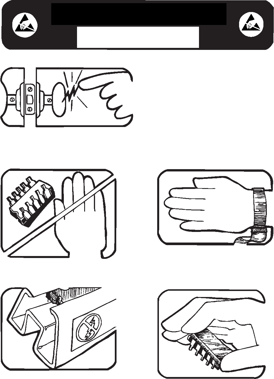
Some semiconductors and custom IC's can be
damaged by electrostatic discharge during
handling. This notice explains how you can
minimize the chances of destroying such devices
by:
1. Knowing that there is a problem.
2. Leaning the guidelines for handling them.
3. Using the procedures, packaging, and
bench techniques that are recommended.
The following practices should be followed to minimize damage to S.S. (static sensitive) devices.
1. MINIMIZE HANDLING
2. KEEP PARTS IN ORIGINAL CONTAINERS
UNTIL READY FOR USE.
3. DISCHARGE PERSONAL STATIC BEFORE
HANDLING DEVICES. USE A HIGH RESIS-
TANCE GROUNDING WRIST STRAP.
4. HANDLE S.S. DEVICES BY THE BODY.
static awareness
A Message From
Fluke Corporation
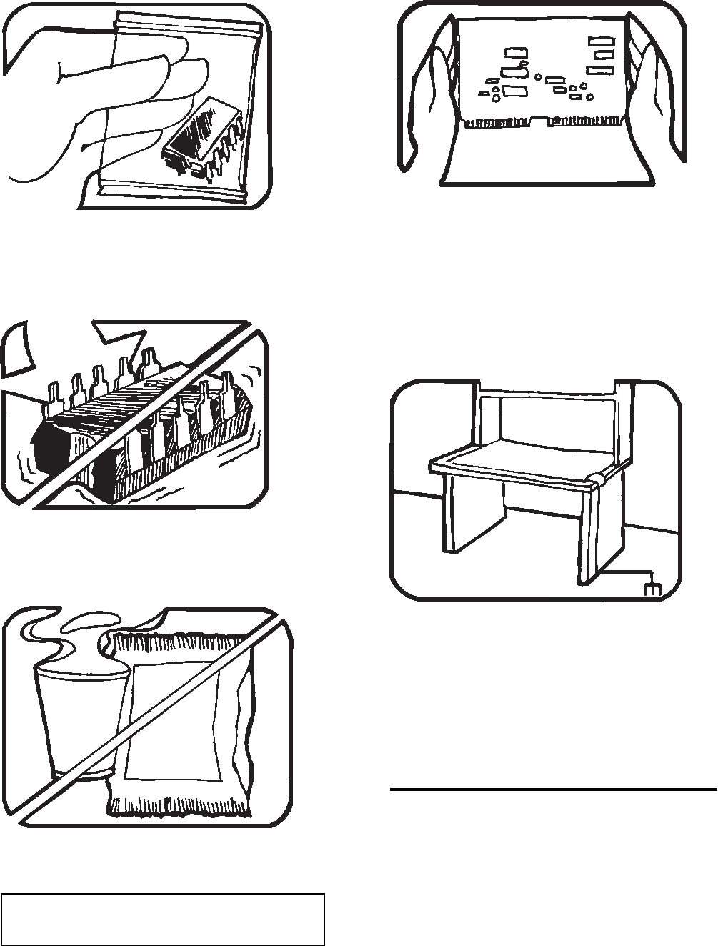
5. USE STATIC SHIELDING CONTAINERS FOR
HANDLING AND TRANSPORT.
6. DO NOT SLIDE S.S. DEVICES OVER
ANY SURFACE.
7. AVOID PLASTIC,VINYL AND STYROFOAM
IN WORK AREA.
8. WHEN REMOVING PLUG-IN ASSEMBLIES
HANDLE ONLY BY NON-CONDUCTIVE
EDGES AND NEVER TOUCH OPEN EDGE
CONNECTOR EXCEPT AT STATIC-FREE
WORK STATION. PLACING SHORTING
STRIPS ON EDGE CONNECTOR HELPS
PROTECT INSTALLED S.S. DEVICES.
9. HANDLE S.S. DEVICES ONLY AT A
STATIC-FREE WORK STATION.
10. ONLY ANTI-STATIC TYPE SOLDER-
SUCKERS SHOULD BE USED.
11. ONLY GROUNDED-TIP SOLDERING
IRONS SHOULD BE USED.
PORTIONS REPRINTED
WITH PERMISSION FROM TEKTRONIX INC.
AND GERNER DYNAMICS, POMONA DIV.
Dow Chemical
4-1
Chapter 4
Maintenance
Title Page
4-1. Introduction .......................................................................................... 4-3
4-2. Cleaning the Air Filter.......................................................................... 4-3
4-3. General Cleaning.................................................................................. 4-4
4-4. Cleaning PCA’s..................................................................................... 4-4
4-5. Access Procedures................................................................................ 4-4
4-6. Top and Bottom Covers................................................................... 4-4
4-7. Digital Section Cover....................................................................... 4-4
4-8. Analog Section Covers..................................................................... 4-4
4-9. Rear Panel Removal and Installation............................................... 4-4
4-10. Rear Panel Assembly Access........................................................... 4-5
4-11. Front Panel Removal and Installation.............................................. 4-6
4-12. Display Assembly Removal and Installation............................... 4-6
4-13. Keyboard Assembly Removal and Installation ........................... 4-7
4-14. Analog Assembly Removal and Installation.................................... 4-7
4-15. Digital Assembly Removal and Installation .................................... 4-9
4-16. Power Transformer Removal and Installation ................................. 4-9
4-17. Hybrid Cover Removal .................................................................... 4-9
4-18. Front/Rear Binding Post Reconfiguration............................................ 4-9
4-19. Installing a Wideband AC Module (Option -03).................................. 4-11
4-20. Clearing Ghost Images from the Control Display................................ 4-11
4-21. Replacing the Clock/Calendar Backup Battery.................................... 4-11
4-22. Using Remote Commands Reserved for Servicing.............................. 4-12
4-23. Using the ETIME Command............................................................ 4-12

5700A/5720A Series II Calibrator
Service Manual
4-2
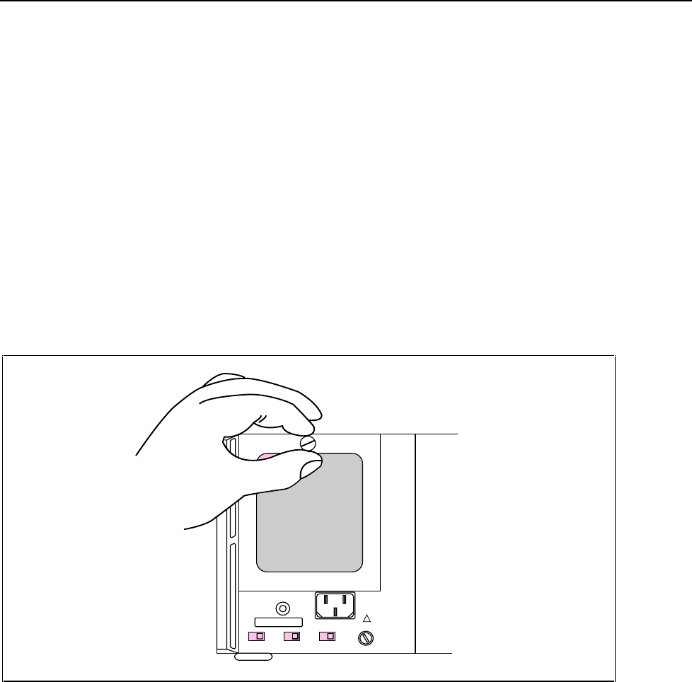
Maintenance
Introduction
4
4-3
4-1. Introduction
This section covers procedures that do not fall into the category of troubleshooting or
repair. This includes access procedures, installation of the Wideband module (Option -
03), periodic cleaning, and other special service procedures.
4-2. Cleaning the Air Filter
CAUTION
Damage caused by overheating may occur if the area around
the fan is restricted, the intake air is too warm, or the air filter
becomes clogged.
The air filter must be removed and cleaned every 30 days or more frequently if the
calibrator is operated in a dusty environment. The air filter is accessible from the rear
panel of the calibrator.
To clean the air filter, refer to Figure 4-1 and proceed as follows:
CHASSIS
GROUND
S2 S3 S4
FUSE -F1
!
F4-1.EPS
Figure 4-1. Air Filter
1. Remove the filter element.
a. Unscrew the knurled screw at the top of the air filter (counterclockwise).
b. Pull the air filter retainer downward; it hinges at the bottom.
c. Remove the filter element.
2. Clean the filter element.
a. Wash the filter element in soapy water.
b. Rinse the filter element in fresh running water.
c. Shake out the excess water, then allow the filter element to dry thoroughly
before reinstalling it.
3. Reinstall the filter element, its retainer, and the knurled screw.

5700A/5720A Series II Calibrator
Service Manual
4-4
4-3. General Cleaning
To keep the Calibrator looking like new, clean the case, front panel keys, and lens using
a soft cloth slightly dampened with water or a non-abrasive mild cleaning solution that
does not harm plastics.
CAUTION
Do not use aromatic hydrocarbons or chlorinated solvents for
cleaning. They can damage the plastic materials used in the
calibrator.
4-4. Cleaning PCA’s
Printed circuit assemblies only need cleaning after repair work. After soldering on a pca,
remove flux residue using isopropyl alcohol and a cotton swab.
4-5. Access Procedures
WARNING
Servicing described in this section is to be performed by
qualified service personnel only. To avoid electrical shock, do
not perform any servicing unless qualified to do so.
4-6. Top and Bottom Covers
Check that power is not connected to the Calibrator; the power control must be off, and
the line power cord must be disconnected. Top and bottom covers are each secured with
eight Phillips head screws (four front, four rear).
4-7. Digital Section Cover
The Digital Section is accessed through one top cover that is secured by six Phillips head
screws.
4-8. Analog Section Covers
The Analog Section is enclosed with separate covers on top and bottom. The top cover is
secured with seven Phillips head screws. The bottom Analog Section cover is secured
with eight Phillips head screws (three short, five longer).
4-9. Rear Panel Removal and Installation
Detach the Rear Panel by removing the six hex head screws (three on each rear handle
side) and the two Phillips head screws found along the side of the Fan Assembly. Refer
to Figure 4-2 for screw locations.
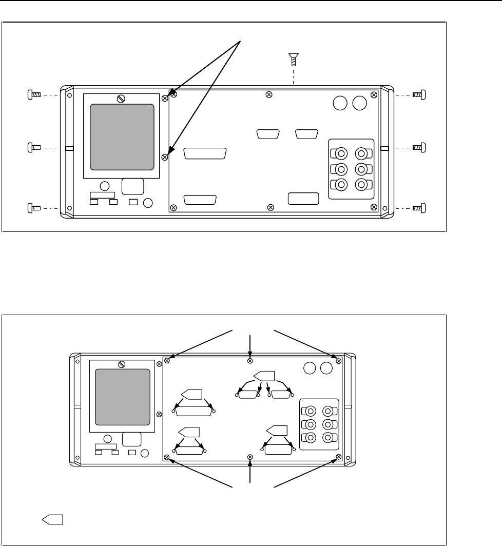
Maintenance
Access Procedures
4
4-5
REMOVE
Figure 4-2. Rear Panel Removal
4-10. Rear Panel Assembly Access
Refer to Figure 4-3 during the following procedure:
REMOVE
REMOVE
1 REMOVE FACK SCREWS TO SEPARATE THE REAR PANEL CIRCUIT BOARD FROM
THE METAL HOUSING.
1
1
1
1
F4-3.EPS
Figure 4-3. Rear Panel Assembly Access
1. Remove the six securing screws for the Rear Panel assembly housing.
2. Gently pull the rear panel housing from the Rear Panel.
3. Allow the rear panel housing to lay flat on the work surface by removing the two
ribbon cables from the Rear Panel board.
4. Remove the two nuts at TB1 and TB2 on the paddle board; separate the associated
wires from the paddle board.
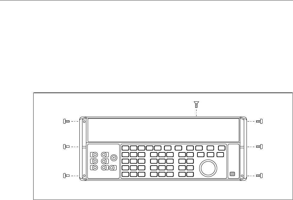
5700A/5720A Series II Calibrator
Service Manual
4-6
5. Remove P11 from J11. Then remove the two paddle board mounting screws and
separate the paddle board from the Rear Panel assembly.
6. Remove the jack screws for each connection on the rear panel housing, then gently
lift the Rear Panel assembly out from the housing.
7. Reverse this procedure to install the Rear Panel assembly.
4-11. Front Panel Removal and Installation
Refer to Figure 4-4 during the following procedure:
F4-4.EPS
Figure 4-4. Front Panel Removal
1. Remove the Calibrator top and bottom covers.
2. Remove the single screw at the top of the Front Panel and the six hex screws on the
front handle sides. Then grasp both handles and gently tilt the Front Panel down and
away from the mainframe, disengaging the green power button. Position the Front
Panel on its handles, in front of the instrument.
3. If you need to completely detach the Front Panel from the Calibrator, one, or
possibly two, cables must be disconnected. The output cable must be detached in all
configurations. If the Wideband Option is installed, you must also detach the related
connector from the Front Panel.
Reverse this procedure to install the Front Panel.
4-12. Display Assembly Removal and Installation
Once the Front Panel has been removed, use the following procedure to access the
Display assembly.
1. Remove the ribbon cable connecting the Display assembly to the Motherboard.
2. Remove the six screws securing the Front Panel Display assembly cover shield.
Three of these screws are accessed from the inside, and the other three are accessed
along the top of the front panel.
3. Remove the seven screws securing the Front Panel Display assembly to the Front
Panel. Gently lift the Front Panel Display assembly up, and remove the keyboard
ribbon cable. Now remove the Front Panel Display assembly.
Reverse this procedure to install the Front Panel Display assembly.

Maintenance
Access Procedures
4
4-7
4-13. Keyboard Assembly Removal and Installation
The following procedure assumes that the Display Assembly Removal procedure has
already been completed.
1. Remove all output cable connections (including GROUND-to-metal) from the front
panel binding posts. Save all removed hardware.
2. Remove the two hex screws at the front of each handle. Then remove the front
handles.
3. Gently release the eight plastic hook catches, and separate the front panel plastic
from the sheet metal.
4. Remove the output adjustment knob flywheel by taking out its center screw. Hold
the wheel in place by inserting a pencil in one of the flywheel holes and pressing on
one of the plastic standoffs.
5. Remove the nine self-tapping screws connecting the Keyboard assembly to the front
panel plastic.
6. Remove the Keyboard assembly by gently releasing the seven plastic hook catches.
Work from one side of the board to the other. Start at either side by simultaneously
releasing a catch and lifting on the board.
Reverse this procedure to install the Keyboard assembly. When reconnecting the wires to
the binding posts, be sure to include a washer on each side of the ring terminals. Refer to
the nearby decal or see sheet 4 of the Analog Motherboard schematic in Section 8 of this
manual for proper connection of the output cable to the front binding posts.
CAUTION
Do not tighten the nuts that hold the wires to the binding posts
more than 7 in-lb. Force exceeding 7 in-lb can destroy the
binding posts.
4-14. Analog Assembly Removal and Installation
The analog assemblies are installed in the sequence shown in Figure 4-5. Note that each
module cannot be positioned in any other slot and that identifying information on the tab
for each module faces forward. In most cases, the component side of each module also
faces forward. The component side faces to the rear for three modules: Current/High
Resolution Oscillator (A7), Ohms Cal (A9), and High Voltage Control (A14). All
modules except the High Voltage Control pull straight up to disengage from the Digital
Motherboard. For the High Voltage Control module, two Phillips head captive screws at
the outer corners of the High Voltage Transformer must be removed before the module
can be removed.
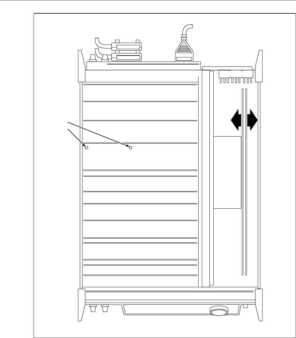
5700A/5720A Series II Calibrator
Service Manual
4-8
VOLTAGE SELECT
SWITCHES
RS232
A5 WIDEBAND OUTPUT PCA
A6 WIDEBAND OSCILLATOR PCA
A7 CURRENT/HIGH-RESOLUTION
OSCILLATOR PCA
A1 KEYBOARD ASSEMBLY
A8 SWITCH MATRIX PCA
A2 FRONT PANEL PCA
A9 OHMS CAL PCA
A10 OHMS MAIN PCA
A11 DAC PCA
A12 OSCILLATOR CONTROL PCA
A13 OSCILLATOR OUTPUT PCA
A14 HIGH VOLTAGE CONTROL PCA
A15 HIGH VOLTAGE/HIGH
CURRENT PCA
A16 POWER AMPLIFIER PCA
A17 REGULATOR/GUARD CROSSING PCA
A18 FILTER/PA SUPPLY PCA
A21 REAR PANEL PCA
A19 DIGITAL POWER SUPPLY PCA
A20 CPU PCA
A22 POWER TRANSFORMER
IEEE
(COMPONENTS
FACE REAR)
(COMPONENTS
FACE REAR)
(COMPONENTS
FACE REAR)
A4 DIGITAL
MOTERBOARD PCA
CAPTIVE
SCREWS
FRONT PANEL
F4-5.EPS
Figure 4-5. Analog and Digital Assemblies
CAUTION
Do not touch any circuit area on an analog assembly.
Contamination from skin oil can produce high resistance paths,
with resulting leakage currents and possible erroneous
readings. Always grasp an analog assembly by its upper corner
ears.

Maintenance
Front/Rear Binding Post Reconfiguration
4
4-9
4-15. Digital Assembly Removal and Installation
Remove the CPU Assembly or the Digital Power Supply Assembly by pulling straight
up at the top corners of the assembly. In relation to the chassis side, the CPU Assembly
components face toward, and the Digital Power Supply Assembly components face
away. See Figure 4-5.
4-16. Power Transformer Removal and Installation
Use the following procedure to remove the Power Transformer assembly:
1. Remove the Calibrator Front and Rear Panels.
2. Remove the Digital Power Supply (A19) and CPU (A20) assemblies.
3. Detach the five connectors leading from the Power Transformer assembly to the
Digital Motherboard. The three connectors at the rear of the assembly may not be
accessible without first removing the rear fan. With the two digital assemblies (A19
and A20) removed, the four Phillips head screws securing this fan can be accessed
through holes in the chassis side.
Note that no two Power Transformer connectors are the same size and that each
connector is keyed; re-connection only involves matching appropriate connectors.
4. Working from the bottom of the instrument, remove the Digital Motherboard (A4)
assembly.
5. Remove the eleven screws securing the Power Transformer assembly, as follows:
• Rear Panel: two screws, which were removed along with the Rear Panel.
• Front Panel: two screws.
• Top Edge: four screws.
• Bottom Edge: three screws.
6. Remove the Power Transformer assembly.
To install the Power Transformer assembly, reverse the preceding six steps.
4-17. Hybrid Cover Removal
When removing the plastic covers from the hybrid assemblies, push the ends of the
cover retainer pins through from the back of the circuit board. The retainer pins can be
damaged by attempting to pull the covers off.
4-18. Front/Rear Binding Post Reconfiguration
An internal cable can be configured for output connections at either the front or rear
binding posts. The front binding posts are usually connected at the factory. If the rear
binding posts are connected at the factory, a decal describing this arrangement is
attached to the front binding posts. The procedure that follows can be used to swap an
existing binding post configuration; it is to be done only at Service Centers. The
following procedure can be used to change front-to-rear or rear-to-front.

5700A/5720A Series II Calibrator
Service Manual
4-10
Reverse this procedure when changing from rear to front output operation.
1. Remove instrument top and bottom covers and remove bottom analog guard cover.
2. Remove the instrument front panel by removing the three hex screws on each front
handle side and a single screw on the top of the front panel. See Figure 4-4 for screw
locations. By grasping the handles gently pull the front panel away from the frame
and lay it on its handles in front of the instrument.
3. Remove all the wires connecting the ring terminals of the output cable to the front
panel binding posts. Save all hardware removed during this step.
4. Remove the two screws and restraining board attaching the toroid to the Front Panel.
Save these items.
5. Position the output cable and toroid along the bottom left side of the instrument. In a
later step, the output cable will be positioned between the Analog Motherboard and
the left side panel.
6. Install the Front Panel.
7. Detach the Rear Panel by removing six hex screws (three on each rear handle side)
and two screws near the the fan filter on the Rear Panel. See Figure 4-2 for screw
locations. Then grasp the handles and gently pull the Rear Panel away from the
frame.
8. Orient the instrument so that it is resting on its right side panel, with its bottom
facing you.
9. Route the output cable between the left side panel and the Analog Motherboard,
ending at the Rear Panel.
10. Using the items obtained during toroid removal, attach the toroid to the two rear
panel standoffs.
11. Attach the color-coded output leads to the rear output binding posts. Use one washer
on each side of each connecting ring. Verify connections by checking the decal
mounted nearby or by matching lead color to the color on the front of the binding
post. (Of the eleven wires, four are clear-insulated shield wires. If necessary, refer to
page 4 of the Analog Motherboard schematic in Section 8 to determine these
connections.)
CAUTION
Do not over tighten hardware on the binding posts. Torque in
excess of seven inch-pounds can damage a binding post.
Note that the I GUARD terminal is not connected at the front binding posts; cut
away the I GUARD thermal fit covering to connect this terminal at the rear binding
posts. Also, the AUX CURRENT ring terminal is not connected at the rear binding
posts; this terminal must be insulated and tied off.
12. Replace the rear panel back, the bottom guard cover, and top and bottom covers to
complete this procedure.

Maintenance
Installing a Wideband AC Module (Option -03)
4
4-11
4-19. Installing a Wideband AC Module (Option -03)
CAUTION
The Wideband option circuit board assemblies contain static-
sensitive components. Use caution to avoid static discharge
when handling the modules.
The procedure that follows can be used to install a 5700A-03 Wideband AC Voltage
module in a Calibrator. The option consists of two circuit board assemblies. This
procedure is to be done only at Service Centers.
1. Remove the top and bottom covers and analog section cover. (See ACCESS
PROCEDURES this section)
2. Referring to Figure 4-5, locate the slots for the Wideband Output Module (A5) and
the Wideband Oscillator Module (A6).
3. Make sure the cable supplied with the Wideband option is connected between the
Wideband Output and Wideband Oscillator assemblies.
4. Uncoil the internal wideband output cable one turn from the Calibrator chassis and
connect it to the coaxial connector on the Wideband Output Module. Make sure the
cable is routed in such a way as to avoid shorting to ground when the board is
installed in the chassis.
5. Install the Wideband Output and Wideband Oscillator Modules and lock the nylon
ears.
6. Run the Wideband Gains Calibration procedure as described in Section 3.
7. Perform the Wideband Flatness Calibration procedure as described in Section 3. The
Wideband option is now installed and ready for use.
4-20. Clearing Ghost Images from the Control Display
After prolonged periods of displaying the same message on the Control Display, you
may notice a non-uniform brightness of pixels across the display. This phenomenon can
be cleared up by lighting up the whole display and leaving it on overnight (or at least
several hours). Proceed as follows to burn in the Control Display:
1. Turn on the Calibrator and press the "Setup Menus" softkey.
2. Press the "Self Test & Diags" softkey.
3. Press the "5700 Self Diags" softkey.
4. Press the "Front Panel Tests" softkey.
5. Under the "Display" label, press the "Control" softkey.
6. Press the "All On" softkey. This causes all Control Display pixels to light. Press the
RESET key or press PREV MENU six times to return to normal operation after an
overnight or equivalent burn in period.
4-21. Replacing the Clock/Calendar Backup Battery
To replace the lithium button-type battery on the CPU Assembly (A20), proceed as
follows:
1. Make sure the power is off and the line power cord disconnected.

5700A/5720A Series II Calibrator
Service Manual
4-12
2. Follow the access procedures to remove the digital side cover.
3. Remove the CPU Assembly (A20).
4. Desolder and remove battery BT1.
5. Solder a replacement battery in place (refer to the parts list for replacement
information if necessary.)
6. Replace the CPU Assembly. After replacing the battery, the setting of the time and
date the elapsed time counter (read by the remote query ETIME? and set by ETIME)
will need to be reprogrammed.
4-22. Using Remote Commands Reserved for Servicing
This information documents remote commands not described in the 5700A/5720A Series
II Operator Manual, Section 5. The commands described here are useful for servicing the
instrument.
4-23. Using the ETIME Command
The ETIME remote command is the companion to ETIME?, the elapsed time query,
which is documented in the Operator Manual. The ETIME? query tells you how many
minutes the Calibrator has been in the power on state since the instrument was built. If
you replace the CPU Assembly (A20), the clock/calendar battery (BT1), or the
clock/calendar IC (U33), you will lose the setting of ETIME. The ETIME command
gives you a way to set this counter to where it was before servicing the instrument. (If
possible, read the counter first using ETIME?.) The syntax for this remote command is
as follows:
ETIME
Description:
Sets the elapsed time counter to any number of minutes from 0 to 2,147,483,647. The
setting of this counter is read by the ETIME? query, described in the 5700A/5720A
Series II Operator Manual. (Sequential command.)
Parameter:
1. SET_TO
2. Integer, number of minutes
Example:
ETIME SET_TO, 4628000
Using The Fatality? and Fatalclr Commands
The FATALITY? query recovers fault codes that were logged when a fatal problem
occurred. These faults are logged into a separate fault queue. Once the faults are read
from the queue, you can clear the queue by sending the FATALCLR command. The
syntax for these remote commands are as follows:

Maintenance
Using Remote Commands Reserved for Servicing
4
4-13
FATALITY?
Description:
Returns the list of the fatal faults logged since the list was last cleared by the
FATALCLR command. (Sequential command.)
Parameter:
None
Response:
(String) The list of faults, one per line in the following format:
<date> <time> <fault code> <fault description string> <EOL>
Example:
"8/30/88 6:33:49 Fault
8/30/88 6:34:05 Fault
8/30/88 6:34:12 Fault
8/30/88 6:34:13 Fault
8/30/88 6:34:14 Fault
8/30/88 6:34:15 Fault
8/30/88 6:34:16 Fault
FATLCLR?
Description:
Clears the list of the fatal faults logged since the list was last cleared by the FATALCLR
command. The list is read by the FATALITY? query. (Sequential command.)
Parameter:
None

5700A/5720A Series II Calibrator
Service Manual
4-14
5-1
Chapter 5
Troubleshooting
Title Page
5-1. Introduction .......................................................................................... 5-3
5-2. Interpreting Diagnostic Fault Codes..................................................... 5-3
5-3. Component-level Troubleshooting....................................................... 5-40
5-4. Troubleshooting the Wideband Output Assembly (A5) .................. 5-40
5-5. Troubleshooting the Wideband Oscillator Assembly (A6) ............. 5-42
5-6. Troubleshooting the Current/Hi-Res Assembly (A7)...................... 5-47
5-7. Current Section............................................................................ 5-47
5-8. Hi-Res Oscillator Section............................................................ 5-52
5-9. Troubleshooting the Switch Matrix Assembly (A8)........................ 5-54
5-10. Troubleshooting the Ohms Cal Assembly (A9)............................... 5-56
5-11. Two-wire Compensation Circuit ................................................. 5-56
5-12. Troubleshooting the Ohms Main Assembly (A10).......................... 5-57
5-13. Troubleshooting the DAC Assembly (A11) .................................... 5-58
5-14. Duty-cycle Control Circuit .......................................................... 5-63
5-15. ADC Circuit................................................................................. 5-67
5-16. Buffered Reference SIP Assembly (A11A2):.............................. 5-68
5-17. Troubleshooting the Oscillator Control Assembly (A12)................ 5-69
5-18. Troubleshooting the Oscillator Output Assembly (A13)................. 5-72
5-19. Troubleshooting the High Voltage Control Assembly (A14).......... 5-74
5-20. Magnitude Control Circuit........................................................... 5-76
5-21. Troubleshooting the High Voltage/High Current Assembly (A15). 5-77
5-22. Troubleshooting the Power Amplifier Assembly (A16).................. 5-79
5-23. Troubleshooting the Filter/PA Supply Assembly (A18) ................. 5-82

5700A/5720A Series II Calibrator
Service Manual
5-2

Troubleshooting
Introduction
5
5-3
5-1. Introduction
Information in this section begins with guidance in using self-diagnostics fault codes to
isolate a faulty module. The descriptive text helps to quickly locate the source of a fault.
Further on, under Component Level Troubleshooting, techniques for isolating faulty
components or circuits are described. The Component Level Troubleshooting is only for
qualified service personnel who do not wish to replace a faulty module through the Fluke
Module Exchange Program. (Refer to Section 1 for module exchange instructions.)
Warning
To avoid electric shock, disconnect all cables from the output
and sense binding posts and do not touch binding post during
self diagnostics.
5-2. Interpreting Diagnostic Fault Codes
Run self diagnostics by pressing the "Setup Menus" then the "Self Test & Diags"
softkey.
Note
Self test diagnostics of the analog circuitry are carried out with the
5700A/5720A Series II binding posts open circuited. (Cables and test
equipment left connected to the binding posts have no effect.)
Test routines connect specific points to the SDL or RCL line and measuring for an
expected voltage and tolerance. The SDL and RCL lines are routed to the adc circuit on
the DAC assembly for measurement.
Fault code descriptions generally indicate the instrument’s test configuration, point being
measured, expected voltage, and probable assembly which is at fault. In some cases, an
addition manual measurement may be required to determine the faulty assembly. These
manual measurements are Noted with the related fault code description. In all cases it is
assumed that the Motherboard assemblies are fully operational. Power Supply faults
assume that other, non-power supply related assemblies are not loading down the Power
Supply.
2700 A7: 8255 Control Word
The diagnostics software reads the control word of the 8255 IC on the Current/Hi Res
assembly. A failure indicates the Current/Hi Res assembly (A7) is probably at fault.
2701 A7: 8255 Port a Fault
The diagnostics software writes and reads data to port A of the 8255 IC on the
Current/Hi Res assembly. A failure indicates the Current/Hi Res assembly (A7) is
probably at fault.
2702 A7: 8255 Port B Fault
The diagnostics software reads port B of the 8255 IC on the Current/Hi Res assembly. A
failure indicates the Current/Hi Res assembly (A7) is probably at fault.
2703 A7: 8255 Port C Fault
The diagnostics software reads port C of the 8255 IC on the Current/Hi Res assembly. A
failure indicates the Current/Hi Res assembly (A7) is probably at fault.

5700A/5720A Series II Calibrator
Service Manual
5-4
2704 Spare
This fault code is not used.
2705 A7: Oven Regulation Fault
The heater voltage of the current hybrid is measured by dividing OVEN TEMP down
and connecting it to the SDL line where it is measured by the adc circuit on the DAC
assembly to ensure the hybrid is warmed up and regulating. OVEN TEMP should be
0.7V ±10% ±0.2V. A failure indicates the Current/Hi Res assembly (A7) is probably at
fault.
2706 A7: Current Compliance Fault
The Current assembly is configured into each of its ranges in both the dc and ac mode.
The output current is connected to the 1.2Ω load resistor. The compliance voltage is
determined by measuring the output side of the shunt resistor via the
Current/Compliance Voltage Monitor circuit. This fault occurs if the voltage is 10% over
the expected. A failure indicates the Current/Hi Res assembly (A7) is probably at fault.
2707 A7: Hardware Initialization Fault
This fault occurs if the diagnostics software was unable to properly set the Current
assembly hardware for diagnostics testing. A failure indicates the Current/Hi Res
assembly (A7) is probably at fault.
2708 Spare
This fault code is not used.
2709 A7: Current Magnitude Fault
The Current assembly is configured into each of its ranges in both the dc and ac mode.
The output current is connected to the 1.2Ω load resistor and the current is calculated by
measuring the voltage drop across the shunt resistance. This fault occurs if the voltage is
10% over the expected. A failure indicates the Current/Hi Res assembly (A7) is probably
at fault.
2710 A7: Dummy Load Current Fault
The Current assembly is configured into each of its dc ranges. The output current is
connected to the 1.2Ω load resistor and the resulting voltage on DUMMY LOAD is
connected to the SDL line where it is measured by the adc circuit on the DAC assembly.
This fault occurs if the current is over 10% ±5 mA of the output current. A failure
indicates the Current/Hi Res assembly (A7) is probably at fault.
2711 Assembly A7 Is Not Responding
At power up the instrument checks to see what assemblies are not installed. This test
verifies that the Current assembly is not responding. A failure indicates the Current/Hi
Res assembly (A7) is probably at fault.
2712 A7: Hi-Res Clock Fault
The Hi-Res clock circuit is checked by connecting HI-RES CLOCK to the SDL line
which is measured by the adc circuit on the DAC assembly for 2.5V ±200 mV. A failure
indicates the Current/Hi Res assembly (A7) is probably at fault.

Troubleshooting
Interpreting Diagnostic Fault Codes
5
5-5
2713 A7: Hi-Res Loop In 100Hz Range
The instrument is set for 2.0V at 100 Hz operation. The input voltage to the VCO circuit
is resistively divided to create the control line HI-RES LOOP. HI-RES LOOP is
connected to the SDL line where it is measured by the adc circuit on the the DAC
assembly. A failure indicates the Current/Hi Res assembly (A7) is probably at fault.
2714 A7: Hi-res Loop In 1kHz Range
The instrument is set for 2.0V at 900 Hz operation. The input voltage to the VCO circuit
is resistively divided to create the control line HI-RES LOOP. HI-RES LOOP is
connected to the SDL line where it is measured by the adc circuit on the the DAC
assembly. A failure indicates the Current/Hi Res assembly (A7) is probably at fault.
2715 A7: Hi-res Loop In 10kHz Range
The instrument is set for 2.0V at 11 kHz operation. The input voltage to the VCO circuit
is resistively divided to create the control line HI-RES LOOP. HI-RES LOOP is
connected to the SDL line where it is measured by the adc circuit on the the DAC
assembly. A failure indicates the Current/Hi Res assembly (A7) is probably at fault.
2716 A7: Hi-res Loop In 100kHz Range
The instrument is set for 2.0V at 70 kHz operation. The input voltage to the VCO circuit
is resistively divided to create the control line HI-RES LOOP. HI-RES LOOP is
connected to the SDL line where it is measured by the adc circuit on the the DAC
assembly. A failure indicates the Current/Hi Res assembly (A7) is probably at fault.
2717 A7: Hi-res Loop In 1MHz Range
The instrument is set for 2.0V at 121 kHz, 600 kHz, and 1.19 MHz operation. The input
voltage to the VCO circuit is resistively divided to create the control line HI-RES LOOP.
HI-RES LOOP is connected to the SDL line where it is measured by the adc circuit on
the the DAC assembly at each frequency. This fault occurs if the VCO input voltage is
not within 25% ±1.0V of the expected voltage. A failure indicates the Current/Hi Res
assembly (A7) is probably at fault.
2718 Fault In Setting Up AC For Diagnostics
This fault occurs if the diagnostics software was unable to properly set the Hi-Resolution
Oscillator hardware for diagnostics testing. A failure indicates the Current/Hi Res
assembly (A7) is probably at fault.
2719 A7: 8255 Was Reset
The control word of the 8255 on the Current/Hi Res assembly is determined to be
incorrect. A failure indicates the Current/Hi Res assembly is probably at fault.
2800 A11: 8255 Control Word
The diagnostics software reads the control word of the 8255 IC on the DAC assembly. A
failure indicates the DAC assembly (A11) is probably at fault.

5700A/5720A Series II Calibrator
Service Manual
5-6
2801 A11: 8255 Port a Wires
The diagnostics software writes and reads data to port A of the 8255 IC on the DAC
assembly. A failure indicates the DAC assembly (A11) is probably at fault.
2802 A11: 8255 Port B Data Bus
The diagnostics software reads port B of the 8255 IC on the DAC assembly. A failure
indicates the DAC assembly (A11) is probably at fault.
2803 A11: 8254 Status Words
The diagnostics software reads the status of the 82C54 IC on the DAC assembly. A
failure indicates the DAC assembly (A11) is probably at fault.
2804 A11: DAC Heaters Not Regulated
The instrument is dormant and the heater voltages (REF HEATER and DCAMP
HEATER) to the hybrid assemblies are measured to be 0.7V ±10% ±0.2V. A failure
indicates the DAC assembly (A11) is probably at fault.
2805 5700 Not Warmed Up
If a heated hybrid assembly in the instrument is detected to not be in regulation the
length of time since the last reset is checked. This fault occurs if the time is less than ten
minutes since a reset.
2806 A11: ADC Amp Output Noise
The instrument is dormant. The ± inputs of the DAC adc amplifier circuit are connected
to common and the adc then takes ten readings. This failure occurs if the difference
between the lowest value and highest value of the ten readings is greater than 500 µV. A
failure indicates the DAC assembly (A11) is probably at fault.
2807 A11: ADC Amp Output Offset
The instrument is dormant. The ±inputs of the DACs adc amplifier circuit are connected
to common and the adc then takes ten readings. This failure occurs if the average of the
ten readings is greater than 3 mV. A failure indicates the DAC assembly (A11) is
probably at fault.

Troubleshooting
Interpreting Diagnostic Fault Codes
5
5-7
2808 A11: ADC Amp Gain Error
The DAC is set to 0.1V on the 11V range and connected to the +input of the DACs adc
amplifier circuit and the -input is connected to common. The adc amplifier has a nominal
gain of 11 resulting in 1.1V at the adc amplifier output. This gain is checked to be 11
±5%. A failure indicates the DAC assembly (A11) is probably at fault.
2809 A11: DAC Monitoring Fault
The DAC is set to 1.0V and routed to the adc circuit via DAC HI DIAG. This 1V from
the DAC is divided by R70 and R84 on the DAC before going to the adc circuit where it
is measured. The DAC is then set to 10V and another reading is taken by the adc. The
exact gain of the divider resistors can now be determined by the formula:
Gain = (10-1V) / (adc10-adc1)
A failure occurs if the detected gain is not within 10% of the nominal 22.13. A failure
indicates the DAC assembly (A11) is probably at fault.
2810 A11: +11V DC Range Fault
The instrument is configured in the +11V dc range. The DAC is sequentially set to 0V,
1V, and 10V. The DAC output is measure at each setting to be within 7% ±10 mV via
DAC HI DIAG by the adc circuit. A failure indicates the DAC assembly (A11) is
probably at fault.
2811 A11: -11V DC Range Fault
The instrument is configured in the -11V dc range. The DAC is sequentially set to 0V,
-1V, and -10V. The DAC output is measure at each setting to be within 7% ±10 mV via
DAC HI DIAG by the adc circuit. A failure indicates the DAC assembly (A11) is
probably at fault.
2812 A11: +22V DC Range Fault
The instrument is configured in the +22V dc range. The DAC is sequentially set to 0V,
2V, and 21.9V. The DAC output is measure at each setting to be within 7.2% ±10 mV
via DAC HI DIAG by the adc circuit. A failure indicates the DAC assembly (A11) is
probably at fault.
2813 A11: -22V DC Range Fault
The instrument is configured in the -22V dc range. The DAC is sequentially set to 0V,
-2V, and -21.9V. The DAC output is measure at each setting to be within 7.2% ±10 mV
via DAC HI DIAG by the adc circuit. A failure indicates the DAC assembly (A11) is
probably at fault.
2814 A11: 6.5V Buffered Reference Fault
The DAC's 6.5V buffered reference (BRF6 and BSRF6) is connected to the -input of the
adc circuit and the DAC output (DAC SENSE CAL) is connected to the +input. The
6.5V buffered reference is measure by adjusting the DAC until a null is achieved. This
fault occurs if the 6.5V buffered reference is over 10% of the nominal. A failure
indicates the DAC assembly (A11) is probably at fault.

5700A/5720A Series II Calibrator
Service Manual
5-8
2815 A11: 6.5V Reference Fault
The DAC’s 6.5V reference (REF6) is connected to the -input of the adc circuit and the
DAC output (DAC SENSE CAL) is connected to the +input. The 6.5V reference is
measure by adjusting the DAC until a null is achieved. This fault occurs if the 6.5V
reference is over 10% of the nominal. A failure indicates the DAC assembly (A11) is
probably at fault.
2816 A11: 13V Buffered Reference Fault
The DAC’s 13V buffered reference (BRF13 and BSRF13) is connected to the -input of
the adc circuit and the DAC output (DAC SENSE CAL) is connected to the +input. The
13V buffered reference is measure by adjusting the DAC until a null is achieved. This
fault occurs if the 13V buffered reference is over 10% of the nominal. A failure indicates
the DAC assembly (A11) is probably at fault.
2817 A11: 13V Reference Fault
The DAC’s 13V reference (REF13) is connected to the -input of the adc circuit and the
DAC output (DAC SENSE CAL) is connected to the +input. The 13V reference is
measure by adjusting the DAC until a null is achieved. This fault occurs if the 13V
reference is over 10% of the nominal. A failure indicates the DAC assembly (A11) is
probably at fault.
2818 Assembly A11 Missing
At power up the instrument checks to see what assemblies are not installed. This test
verifies that the DAC assembly is not responding. A failure indicates the DAC assembly
(A11) is probably at fault.
2819 A11: 8255 Was Reset
The control word of the 8255 on the DAC assembly is read. A failure indicates the DAC
assembly (A11) is probably at fault.
2820 A11: Fine Adjust Channel Fault
The second channel of the DAC assembly is tested. The second channel is set to a count
which gives 0V at the DAC output. The output is measured by the adc circuit. The
second channel count is increased and the increase in the DAC output is verified. A
failure indicates the DAC assembly (A11) is probably at fault.
2821 A8/A11: +11/22V DC Zero Estimate Fault
The DAC is in either the +11V or +22V range. Its output (DAC SENSE CAL) is
connected to the +input of the adc circuit and the -input of the adc circuit is connected to
RCOM. The zero is estimated by adjusting the DAC until a null is achieved. This fault
occurs when the nulling process does not converge. A failure indicates the DAC
assembly (A11) is probably at fault.

Troubleshooting
Interpreting Diagnostic Fault Codes
5
5-9
2822 A8/A11: -11/22V DC Zero Estimate Fault
The DAC is in either the -11V or -22V range. Its output (DAC SENSE CAL) is
connected to the +input of the adc circuit and the -input is connected to RCOM. The zero
is estimated by adjusting the DAC until a null is achieved. This fault occurs when the
nulling process does not converge. A failure indicates the DAC (A11) assembly is
probably at fault.
2823 A11: Couldn’t Estimate +11V Or 22V Gain
One of the DAC’s references is connected to the -input of the adc circuit and DAC output
(DAC SENSE CAL) is connected to the +input. The gain is estimated by adjusting the
DAC until a null is achieved. This fault occurs when the nulling process does not
converge. A failure indicates the DAC (A11) assembly is probably at fault.
2824 A11: Couldn’t Estimate 6.5 MHz Or 13 MHz Ref
One of the DAC’s references is connected to the -input of the adc circuit and DAC output
(DAC SENSE CAL) is connected to the +input. The reference is estimated by adjusting
the DAC until a null is achieved. This fault occurs when the nulling process does not
converge. A failure indicates the DAC assembly (A11) is probably at fault.
2825 A11: Couldn’t Est 6.5V Or 13V Buf Ref
One of the DAC’s buffered references is connected to the -input of the adc circuit and
DAC output (DAC SENSE CAL) is connected to the +input. The buffered reference is
estimated by adjusting the DAC until a null is achieved. This fault occurs when the
nulling process does not converge. A failure indicates the DAC (A11) assembly is
probably at fault.
2826 A11: A/D Overload Fault
The adc on the DAC assembly is tested by putting a positive overload then a negative
overload into the adc input. The adc output is read and compared against an expected
overload reading for both the positive and negative overload. If either of these tests fail
the fault message is sent. A failure on either of these tests indicates that the DAC
assembly (A11) is at fault.
3100 A14: 8255 Control Word
The diagnostics software read the control word of the 8255 IC on the High Voltage
Control assembly. A failure indicates the High Voltage Control assembly (A14) is
probably at fault.
3101 A14: 8255 Port a Fault
The diagnostics software writes and reads data to port A of the 8255 IC on the High
Voltage Control assembly. A failure indicates the High Voltage Control assembly (A14)
is probably at fault.
3102 A14: 8255 Port B Fault
The diagnostics software reads port B of the 8255 IC on the High Voltage Control
assembly. A failure indicates the High Voltage Control assembly (A14) is probably at
fault.

5700A/5720A Series II Calibrator
Service Manual
5-10
3103 A14: 8255 Port C Fault
The diagnostics software reads port C of the 8255 IC on the High Voltage Control
assembly. A failure indicates the High Voltage Control assembly (A14) is probably at
fault.
3104 A15: HV Oven Regulation Fault
The heater voltage of the High Voltage/High Current assembly HR7 hybrid is divided by
11 and is measured by the adc circuit. The heater voltage should be 0.7V ±10% ±0.2V. If
it is out of tolerance, the High Voltage/High Current assembly (A15) is probably at fault.
3105 A15: HV I Oven Regulation Fault
The heater voltage of the High Voltage/High Current assembly H4 hybrid is routed to
the High Voltage Control assembly via HV MUX0. The High Voltage Control connects
HV MUX0 to the SDL which is routed to the DAC assembly where it is measured by the
adc circuit to be 0.7V ±10% ±0.2V. A failure indicates the High Voltage/High Current
assembly (A15) is probably at fault.
3106 A15: DC HV Amp Noise Fault
The High Voltage assemblies are configured in the dormant state with the exception that
the DAC output, set to 0.0V, is connected to the DC HV AMPLIFIER/AC SENSE
BUFFER circuit of the High Voltage/High Current assembly. This circuit is configured
as an amplifier with a gain of 100 whose output is connected to the RCL line. The RCL
line is routed to the DAC assembly where it is measured by the adc circuit. The adc
circuit takes ten readings and this failure occurs if the difference between the lowest
value and highest value of the ten readings is over 0.001V. A failure indicates the High
Voltage/High Current assembly (A15) is probably at fault.
3107 A15: DC HV Amp Offset Fault
The High Voltage assemblies are configured in the dormant state with the exception that
the DAC output, set to 0.0V, is connected to the DC HV AMPLIFIER/AC SENSE
BUFFER circuit of the High Voltage/High Current assembly. This circuit is configured
as an amplifier with a gain of 100 whose output is connected to the RCL line. The RCL
line is routed to the DAC assembly where it is measured by the adc circuit. The adc
circuit takes ten readings and this failure occurs if the average value is over 0.003V. A
failure indicates the High Voltage/High Current assembly (A15) is probably at fault.
3108 A15: DC HV Amp Gain Fault
The High Voltage assemblies are configured in the dormant state with the exception that
the DAC output, set to -0.001V, is connected to the DC HV AMPLIFIER/AC SENSE
BUFFER circuit of the High Voltage/High Current assembly. This circuit is configured
as an amplifier with a gain of -100 resulting in 0.1V at the output which is connected to
the RCL line. The RCL line is routed to the DAC assembly where it is measured by the
adc circuit. The gain of this circuit is determined by this reading along with the
previously checked offset. This failure occurs if the determined gain is over 6% of the
nominal -100. A failure indicates the High Voltage/High Current assembly (A15) is
probably at fault.

Troubleshooting
Interpreting Diagnostic Fault Codes
5
5-11
3109 A15: HV +DC Preamplifier Fault
The instrument is set to the dc 1100V range with the amplitude set to 220V, 600V, and
1100V. The output of the DC HV AMPLIFIER/AC SENSE BUFFER circuit of the High
Voltage/High Current assembly is measured for 0.55V ±0.2V. This voltage is divided to
create HV MUX2 which is routed to Diagnostic circuit on the High Voltage Control
assembly where it is connected to the SDL line for measurement by the adc circuit on the
DAC assembly.
3110 A15: HV +DC Series Pass & Current Fault
The instrument is set to the dc 1100V range with the amplitude set to 220V, 600V, and
1100V. HV MUX3 from the HV DC OUTPUT SERIES PASS & CURRENT LIMIT
circuit on the High Voltage/High Current assembly is measured for -0.035V ±0.02V. HV
MUX3 is routed to Diagnostic circuit on the High Voltage Control assembly where it is
connected to the SDL line for measurement by the adc circuit on the DAC assembly.
3111 A15: HV +DC High Voltage Output Fault
The instrument is set to the dc 1100V range with the amplitude set to 220V, 600V, and
1100V. This output voltage is divided to create MUX5 which is connected to the SDL
line for measurement by the adc circuit on the DAC assembly. This failure occurs if the
expected output voltage is not within 12% of the nominal.
3112 A15: HV +DC Ref/error Amplitude Fault
The instrument is set to the dc 1100V range with the amplitude set to 220V, 600V, and
1100V. The control signal AMPLITUDE from the Magnitude Control circuitry of the
High Voltage Control assembly is measured. The nominal gain from AMPLITUDE to
HV OUT is 135. This gain is checked by measuring AMPLITUDE to be 0.0074 of the
nominal output ±25%. AMPLITUDE is divided to create MUX7 which is connected to
the SDL line for measurement by the adc circuit on the DAC assembly.
3113 A15: HV -DC Preamplifier Fault
The instrument is set to the dc 1100V range with the amplitude set to -220V, -600V, and
-1100V. The output of the DC HV AMPLIFIER/AC SENSE BUFFER circuit of the
High Voltage/High Current assembly is measured for 2.3V ±0.2V. This voltage is
divided to create HV MUX2 which is routed to Diagnostic circuit on the High Voltage
Control assembly where it is connected to the SDL line for measurement by the adc
circuit on the DAC assembly.
3114 A15: HV -DC Series Pass & Current Fault
The instrument is set to the dc 1100V range with the amplitude set to -220V, -600V, and
-1100V. HV MUX3 from the HV DC OUTPUT SERIES PASS & CURRENT LIMIT
circuit on the High Voltage/High Current assembly is measured for -0.035V ±0.02V. HV
MUX3 is routed to Diagnostic circuit on the High Voltage Control assembly where it is
connected to the SDL line for measurement by the adc circuit on the DAC assembly.
3115 A15: HV -DC High Voltage Output Fault
The instrument is set to the dc 1100V range with the amplitude set to -220V, -600V, and
-1100V. This output voltage is divided to create MUX5 which is connected to the SDL

5700A/5720A Series II Calibrator
Service Manual
5-12
line for measurement by the adc circuit on the DAC assembly. This failure occurs if the
expected output voltage is not within 12% of the nominal.
3116 A15: HV -DC Reference/error Amp Fault
The instrument is set to the dc 1100V range with the amplitude set to -220V, -600V, and
-1100V. The control signal AMPLITUDE from the Magnitude Control circuitry of the
High Voltage Control assembly is measured. The nominal gain from AMPLITUDE to
HV OUT is 135. This gain is checked by measuring AMPLITUDE to be 0.0074 of the
nominal output ±25%. AMPLITUDE is divided to create MUX7 which is connected to
the SDL line for measurement by the adc circuit on the DAC assembly.
3117 A14/A15: HV +DC Current Error Amp Fault
The Calibrator is set to the dc +2.2A current range with the amplitude set to +0.22A,
+0.6A, and +1.2A. The control signal AMPLITUDE from the magnitude control
circuitry of the High Voltage Control assembly is measured to be within 25% of the
expected value. AMPLITUDE is divided to create MUX7 which is connected to the SDL
line for measurement by the adc circuit on the DAC assembly.
3118 A14/A15: HV -DC Current Error Amp Fault
The Calibrator is set to the dc -2.2A current range with the amplitude set to -1.2A. The
control signal AMPLITUDE from the magnitude control circuitry of the High Voltage
Control assembly is measured to be within 25% of the expected value. AMPLITUDE is
divided to create MUX7 which is connected to the SDL line for measurement by the adc
circuit on the DAC assembly.
3119 A14/A15: HV +DC Current Abs. Value
The instrument is configured to the +DC 2.2A range and set for an output of 0.22A,
0.60A, and 1.2A. The output current from the High Voltage/High Current assembly is
routed to the Current assembly where it is connected to the 1.2Ω load resistor. The
Current control signal G OUT from the High Voltage/High Current assembly is routed to
the Absolute Value Circuit on the High Voltage Control. The output from the Absolute
Value circuit should be = 2.17 * I, ±25%, where "I" is the output current. This voltage is
divided creating MUX6 which is connected to the SDL line where it is measured by the
adc circuit on the DAC assembly.
3120 A14/A15: HV -DC Current Abs. Value
The instrument is configured to the -DC 2.2A range and set for an output of -1.2A. The
output current from the High Voltage/High Current assembly is routed to the Current
assembly where it is connected to the 1.2Ω load resistor. The Current control signal G
OUT from the High Voltage/High Current assembly is routed to the Absolute Value
Circuit on the High Voltage Control. The output from the Absolute Value circuit is a
positive voltage which should be = 2.17 * I, ±25%, where "I" is the output current. This
voltage is divided creating MUX6 which is connected to the SDL line where it is
measured by the adc circuit on the DAC assembly.
3121 Spare
This fault code is not used.

Troubleshooting
Interpreting Diagnostic Fault Codes
5
5-13
3122 A14/A15: HV AC 1kHz, Preamp (Lo)
The instrument is configured to the ac 1100V range with on amplitude of 220V at 1 kHz.
The output of the DC HV AMPLIFIER/AC SENSE BUFFER circuit of the High
Voltage/High Current assembly is measured for 0.0V ±0.2V. This voltage is divided to
create HV MUX2 which is routed to Diagnostic circuit on the High Voltage Control
assembly where it is connected to the SDL line for measurement by the adc circuit on the
DAC assembly.
3123 A14/A15: HV AC 1kHz, Preamp (Mid)
The instrument is configured to the ac 1100V range with on amplitude of 600V at 1 kHz.
The output of the DC HV AMPLIFIER/AC SENSE BUFFER circuit of the High
Voltage/High Current assembly is measured for 0.0V ±0.2V. This voltage is divided to
create HV MUX2 which is routed to Diagnostic circuit on the High Voltage Control
assembly where it is connected to the SDL line for measurement by the adc circuit on the
DAC assembly.
3124 A14/A15: HV AC 1kHz, Preamp (Hi)
The instrument is configured to the ac 1100V range with on amplitude of 1100V at 1
kHz. The output of the DC HV AMPLIFIER/AC SENSE BUFFER circuit of the High
Voltage/High Current assembly is measured for 0.0V ±0.2V. This voltage is divided to
create HV MUX2 which is routed to Diagnostic circuit on the High Voltage Control
assembly where it is connected to the SDL line for measurement by the adc circuit on the
DAC assembly.
3125 A14/A15: HV AC 100Hz, Preamp (Lo)
The instrument is configured to the ac 1100V range with on amplitude of 220V at 50 Hz.
The output of the DC HV AMPLIFIER/AC SENSE BUFFER circuit of the High
Voltage/High Current assembly is measured for 0.0V ±0.2V. This voltage is divided to
create HV MUX2 which is routed to Diagnostic circuit on the High Voltage Control
assembly where it is connected to the SDL line for measurement by the adc circuit on the
DAC assembly.
3126 A14/A15: HV AC 100Hz, Preamp Fault
The instrument is configured to the ac 1100V range with on amplitude of 600V at 50 Hz.
The output of the DC HV AMPLIFIER/AC SENSE BUFFER circuit of the High
Voltage/High Current assembly is measured for 0.0V ±0.2V. This voltage is divided to
create HV MUX2 which is routed to Diagnostic circuit on the High Voltage Control
assembly where it is connected to the SDL line for measurement by the adc circuit on the
DAC assembly.
3127 A14/A15: HV AC 100Hz, Preamp (Hi)
The instrument is configured to the ac 1100V range with on amplitude of 1100V at 50
Hz. The output of the DC HV AMPLIFIER/AC SENSE BUFFER circuit of the High
Voltage/High Current assembly is measured for 0.0V ±0.2V. This voltage is divided to
create HV MUX2 which is routed to Diagnostic circuit on the High Voltage Control
assembly where it is connected to the SDL line for measurement by the adc circuit on the
DAC assembly.

5700A/5720A Series II Calibrator
Service Manual
5-14
3128 A14/A15: HV AC 1kHz, Output (Lo)
The instrument is configured to the ac 1100V range with on amplitude of 220V at 1 kHz.
The high voltage output is divided and converted to a dc voltage by the OUTPUT PEAK
MEASURE circuit to create MUX5. This dc voltage is equal to the positive peaks of the
ac amplitude. MUX5 is connected to the SDL line for measurement by the adc circuit on
the DAC assembly. The high voltage output is measured for 220V ±12%. A failure
indicates the High Voltage Control assembly (A14) is probably at fault.
3129 A14/A15: HV AC 1kHz, Output (Mid)
The instrument is configured to the ac 1100V range with on amplitude of 600V at 1 kHz.
The high voltage output is divided and converted to a dc voltage by the OUTPUT PEAK
MEASURE circuit to create MUX5. This dc voltage is equal to the positive peaks of the
ac amplitude. MUX5 is connected to the SDL line for measurement by the adc circuit on
the DAC assembly. The high voltage output is measured for 600V ±12%. A failure
indicates the High Voltage Control assembly (A14) is probably at fault.
3130 A14/A15: HV AC 1kHz, Output (Hi)
The instrument is configured to the ac 1100V range with on amplitude of 1100V at 1
kHz. The high voltage output is divided and converted to a dc voltage by the OUTPUT
PEAK MEASURE circuit to create MUX5. This dc voltage is equal to the positive peaks
of the ac amplitude. MUX5 is connected to the SDL line for measurement by the adc
circuit on the DAC assembly. The high voltage output is measured for 1100V ±12%. A
failure indicates the High Voltage Control assembly (A14) is probably at fault.
3131 A14/A15: HV AC 100Hz, Output (Lo)
The instrument is configured to the ac 1100V range with on amplitude of 220V at 50 Hz.
The high voltage output is divided and converted to a dc voltage by the OUTPUT PEAK
MEASURE circuit to create MUX5. This dc voltage is equal to the positive peaks of the
ac amplitude. MUX5 is connected to the SDL line for measurement by the adc circuit on
the DAC assembly. The high voltage output is measured for 220V ±12%. A failure
indicates the High Voltage Control assembly (A14) is probably at fault.
3132 A14/A15: HV AC 100Hz, Output (Mid)
The instrument is configured to the ac 1100V range with on amplitude of 600V at 50 Hz.
The high voltage output is divided and converted to a dc voltage by the OUTPUT PEAK
MEASURE circuit to create MUX5. This dc voltage is equal to the positive peaks of the
ac amplitude. MUX5 is connected to the SDL line for measurement by the adc circuit on
the DAC assembly. The high voltage output is measured for 600V ±12%. A failure
indicates the High Voltage Control assembly (A14) is probably at fault.
3133 A14/A15: HV AC 100Hz, Output (Hi)
The instrument is configured to the ac 1100V range with on amplitude of 1100V at 50
Hz. The high voltage output is divided and converted to a dc voltage by the OUTPUT
PEAK MEASURE circuit to create MUX5. This dc voltage is equal to the positive peaks
of the ac amplitude. MUX5 is connected to the SDL line for measurement by the adc
circuit on the DAC assembly. The high voltage output is measured for 1100V ±12%. A
failure indicates the High Voltage Control assembly (A14) is probably at fault.

Troubleshooting
Interpreting Diagnostic Fault Codes
5
5-15
3134 Spare
This fault code is not used.
3135 Assembly A14 Not Responding
At power up the instrument checks to see what assemblies are not installed. This test
verifies that the High Voltage Control assembly is not responding. A failure indicates the
High Voltage Control assembly is probably at fault.
3136 A14: 8255 Was Reset
The control word for the 8255 on the High Voltage Control assembly is read. A failure
indicates the High Voltage Control assembly (A14) is probably at fault.
3137 A14/A15/A16: 2.2A AC Range Mag. Fault
The instrument is configured to the ac 2.2A range and set to 0.22A at 1 kHz, 0.6A at 1
kHz, 1.1A at 1 kHz, 0.6A at 40 Hz, and 1.1A at 50 Hz. The output current from the High
Voltage/High Current assembly is routed to the Current assembly where it is connected
to the 1.2Ω load resistor. The input current from the Current assembly is is measured at
each setting by measuring the voltage drop across the 22 mA range shunt resistor on the
Current assembly. This voltage drop is measured to be within 10% ±20 µV of the
nominal. A failure indicates the High Voltage/High Current assembly (A15) is probably
at fault.
3138 A14/A15/A16: 2.2A AC Range Compliance
The instrument is configured to the ac 2.2A range and set to 0.22A at 1 kHz, 0.6A at 1
kHz, 1.1A at 1 kHz, 0.6A at 40 Hz, and 1.1A at 50 Hz. The output current from the High
Voltage/High Current assembly is routed to the Current assembly where it is connected
to the 1.2Ω load resistor. The compliance voltage is determined by measuring the output
side of the 22 mA range shunt resistor on the Current assembly. This is done via the
Current Compliance Monitor circuit on the Current assembly and is checked to be less
than 10V. A failure indicates the High Voltage/High Current assembly is probably at
fault.
3139 A14/A15/A16: 2.2A AC Range Amplitude
The instrument is configured to the ac 2.2A range and set for an output current of 0.22A
at 1 kHz, 0.6A at 1 kHz, 1.1A at 1 kHz, 0.6A at 40 Hz, and 1.1A at 50 Hz. The output
current from the High Voltage/High Current assembly is routed to the Current assembly
where it is connected to the 1.2Ω load resistor. The Current control signal G OUT from
the High Voltage/High Current assembly is routed to the Magnitude Control circuit of
the High Voltage Control assembly. The control signal AMPLITUDE is measured to be
= I * 4.23 + 4.447, ±20%. This voltage is divided creating MUX7 which is connected to
the SDL line where it is measured by the adc circuit on the DAC assembly.

5700A/5720A Series II Calibrator
Service Manual
5-16
3140 A14/A15/A16: 2.2A AC Range Abs. Value
The instrument is configured to the ac 2.2A range and set for an output current of 0.22A
at 1 kHz, 0.6A at 1 kHz, 1.1A at 1 kHz, 0.6A at 40 Hz, and 1.1A at 50 Hz. The output
current from the High Voltage/High Current assembly is routed to the Current assembly
where it is connected to the 1.2Ω load resistor. The Current control signal G OUT from
the High Voltage/High Current assembly is routed to the Absolute Value Circuit on the
High Voltage Control. The output from the Absolute Value circuit is a positive voltage
which should be = 3.07 * I, ±10%, where "I" is the output current. This voltage is
divided creating MUX6 which is connected to the SDL line where it is measured by the
adc circuit on the DAC assembly.
3141 A14/A15/A16: 2.2A DC Range Dummy Load
The instrument is configured to the dc 2.2A range. The output current from the High
Voltage/High Current assembly is routed to the Current assembly where it is connected
to the 1.2Ω load resistor. The resulting voltage across this load resistor is measured by
connected DUMMY LOAD on the Current assembly to the SDL line where it is
measured by the adc circuit on the DAC assembly. This fault occurs if the determined
current is over 10% ±5 mA of the nominal. A failure indicates the High Voltage/High
Current assembly (A15) is probably at fault.
3142 A14/A15/A16: 2.2A DC Range Compliance
The instrument is configured to the dc 2.2A range. The output current from the High
Voltage/High Current assembly is routed to the Current assembly where it is connected
to the 1.2Ω load resistor. The compliance voltage is determined by measuring the output
side of the 22 mA range shunt resistor on the Current assembly. This is done via the
Current Compliance Monitor circuit on the Current assembly and is checked to be less
than 10V. A failure indicates the High Voltage/High Current assembly is probably at
fault.
3143 A14/A15/A16: 2.2A DC Range Magnitude
The instrument is configured to the dc 2.2A range. The output current from the High
Voltage/High Current assembly is routed to the Current assembly where it is connected
to the 1.2Ω load resistor. The output current is calculated by measuring the voltage drop
across the 22 mA range shunt resistor on the Current assembly. This fault occurs if the
determined current is over 10% of the nominal. A failure indicates the High
Voltage/High Current assembly (A15) is probably at fault.
3300 A9: 8255 Control Word
The diagnostics software reads the control word of the 8255 IC on the Ohms Cal
assembly (A9). A failure indicates the Ohms Cal assembly (A9) is probably at fault.
3301 A9: 8255 Port a Fault
The diagnostics software writes and reads data to port A of the 8255 IC on the Ohms Cal
assembly (A9). A failure indicates the Ohms Cal assembly (A9) is probably at fault.
3302 A9: 8255 Port B Fault
The diagnostics software reads port B of the 8255 IC on the Ohms Cal assembly (A9)
during the instruments dormant state. A failure indicates the Ohms Cal assembly (A9) is
probably at fault.

Troubleshooting
Interpreting Diagnostic Fault Codes
5
5-17
3303 A9: 8255 Port C Fault
The diagnostics software reads port C of the 8255 IC on the Ohms Cal assembly (A9)
during the instruments dormant state. A failure indicates the Ohms Cal assembly (A9) is
probably at fault.
3304 A9: 10V Source Fault
The 2/5/10V SOURCE circuit on the Ohms Cal assembly (A9) is set for 10V and routed
to the adc circuit on the DAC assembly, via the SDL line, where it is measured for 10V
±7%. This 10V can be verified with a DMM, hi to TP13 and low to TP12. If the
measured voltage is out of tolerance, the 2/5/10V SOURCE circuit on the Ohms Cal
assembly (A9) is faulty. If the measured voltage is within tolerance, the diagnostic
circuit on the Ohms Cal assembly (A9) is probably at fault.
Note
If extender cards are available, verify that 10V SENSE LOis tied to SCOM.
This connection is done with relays onboth the Ohms assemblies.
3305 A9: 5V Source Fault
The 2/5/10V SOURCE circuit on the Ohms Cal assembly (A9) is set for 5V and routed
to the adc circuit on the DAC assembly, via the SDL line, where it is measured for 5V
±7%. A failure indicates the 2/5/10V SOURCE circuit on the Ohms Cal assembly (A9)
is probably at fault.
Note
If extender cards are available verify that 10V SENSE LOis tied to SCOM.
This connection is done with relays onboth the Ohms assemblies.
3306 A9: 2V Source Fault
The 2/5/10V SOURCE circuit on the Ohms Cal assembly (A9) is set for 2V and routed
to the adc circuit on the DAC assembly, via the SDL line, where it is measured for 2V
±7%. A failure indicates the 2/5/10V SOURCE circuit on the Ohms Cal assembly (A9)
is probably at fault.
Note
If extender cards are available verify that 10V SENSE LOis tied to SCOM.
This connection is done with relays onboth the Ohms assemblies.
3307 Spare
This fault code is not used.
3308 A9: Diff Amp Offset Fault
The offset of the Differential Amplifier circuit on the Ohms Cal assembly (A9) is
checked. The DAC output is set to 0V and connected to both the ±inputs of the
Differential Amplifier circuit. The output is routed to the adc circuit on the DAC
assembly via the RCL line. Ten reading are taken and this fault occurs of the difference
between the lowest and highest value if over 1 mV or if the absolute value is over

5700A/5720A Series II Calibrator
Service Manual
5-18
10 mV. A failure indicates the Differential Amplifier circuit on the Ohms Cal assembly
(A9) is probably at fault.
3309 A9: Diff Amp Gain Fault
The gain (nominal gain of 75) Differential Amplifier circuits on the Ohms Cal assembly
(A) is checked. The DAC output is set to 86.7 mV and connected to the -input of the Diff
Amp circuit with the +input connected to RCOM. The output of the Diff Amp circuit is
routed to the adc circuit on the DAC assembly, via the RCL line, where it is compared to
the 6.5V reference. This fault occurs if the determined gain is over 6% from the nominal
75. A failure indicates the Differential Amplifier circuit on the Ohms Cal assembly (A9)
is probably at fault.
3310 A9: Diff Amp Noise Fault
The noise of the differential amplifier circuit on the Ohms Cal assembly (A9) is checked.
The DAC output is set to 0V and connected to both the ±inputs of the differential
amplifier circuit. The output is routed to the adc circuit on the DAC assembly via the
RCL line. Ten readings are taken and this fault occurs if the difference between the
lowest and highest value if over 1 mV. A failure indicates the differential amplifier
circuit on the Ohms Cal assembly (A9) is probably at fault.
3311 A9/A10: Ohms 10:1 Divider Fault
The 2/5/10V SOURCE circuit is set for 10V and connected across the 100 kΩ resistance
in Z5 on the Ohms Cal assembly (A9). The resulting 1V across the 10 kΩ portion is
measure for 1V ±3% ±15 mV. A failure indicates the Ohms Cal assembly (A9) is
probably at fault.
3312 A9/A10: Ohms 1:1 Divider Fault
The 2/5/10V SOURCE circuit is set for 10V and connected across the 100 kΩ resistance
in Z5 on the Ohms Cal assembly (A9). This arrangement is measured for 10V ±3% ±15
mV. A failure indicates the Ohms Cal assembly (A9) is probably at fault.
3313 A9/A10: 10 Kilohm Diagnostic Fault
The 2/5/10V SOURCE circuit is set for 10V and connected across the 20 kΩ resistance
made from the 10 kΩ in Z5 on the Ohms Cal assembly, (A9) and the 10 kΩ string on the
Ohms Main assembly (A10) connected in series. The resulting 5V across the 10 kΩ
string on the Ohms Main assembly is measured for 5V ±3% ±15 mV. Measure the 5V
across the 10 kΩ string by connecting a DMM hi to TP2 and low to TP1 on the Ohms
Cal assembly (A9). If this voltage is greater than 5V the Ohms Main assembly (A10) is
probably at fault. If the voltage is less than or equal to 5V the Ohms Cal assembly (A9)
is probably at fault.
3314 A9/A10: 19 Kilohm Cal Diag Fault
The 2/5/10V SOURCE circuit is set for 10V and connected across the 29 kΩ resistance
made from the 10 kΩ in Z5 on the Ohms Cal assembly, (A9) and the 19 kΩ string on the
Ohms Main assembly (A10) connected in series. The resulting 6.55V across the 19kΩ
string on the Ohms Main assembly is measured for 6.55V ±3% ±15 mV. A failure
indicates the Ohms Main assembly (A10) is probably at fault.

Troubleshooting
Interpreting Diagnostic Fault Codes
5
5-19
3315 A9/A10: 10 Ohm Cal Diag Fault
The 2/5/10V SOURCE circuit is set for 2V and connected across the 100Ω string on the
Ohms Main assembly. The resulting 0.2 V across the 10Ω portion is connected to the -
input of the Differential Amplifier on the Ohms Cal assembly. The output of the DAC
assembly is set to 2V and connected across the 100 kΩ resistance in Z5 on the Ohms Cal
assembly. The resulting 0.2V across the 10 kΩ portion of Z5 is connected to the +input
of the Differential Amplifier. The output of the Differential Amplifier is routed to the
adc circuit on the DAC assembly, via the RCL line, and measured for 0V ±3% ±15 mV.
Verify that the divided DAC voltage of 0.2V ±5% is at the +input of the Diff Amp by
connecting DMM hi to TP20 and low to TP10 of the Ohms Cal assembly. If this
measured voltage is out of tolerance, the Ohms Cal assembly (A9) is probably at fault.
3316 A9/A10: 19 Ohm Cal Diag Fault
The 2/5/10V SOURCE circuit is set for 2V and connected across the 190Ω string on the
Ohms Main assembly. The resulting 0.2V across the 10Ω portion is connected to the -
input of the Differential Amplifier on the Ohms Cal assembly. The output of the DAC
assembly is set to 2V and connected across the 100 kΩ resistance in Z5 on the Ohms Cal
assembly. The resulting 0.2V across the 10 kΩ portion of Z5 is connected to the +input
of the Differential Amplifier. The output of the Differential Amplifier is routed to the
adc circuit on the DAC assembly, via the RCL line, and measured for 0V ±3% ±15 mV.
A failure indicates the calibration of the 19Ω resistance on the Ohms Main assembly
(A10) is probably at fault.
3317 A9/A10: 100 Kilohm Ratio Fault
The 2/5/10V SOURCE circuit on the Ohms Cal assembly is set to 10V which is routed to
the Ohms Main assembly and connected to the 100 kΩ string. The resulting 1V across
the 10 kΩ portion is measured for 1V ±3% ±15 mV. A failure indicated the Ohms Main
assembly (A10) is probably at fault.
3318 A9/A10: 190 Kilohm Ratio Fault
The 2/5/10V SOURCE circuit on the Ohms Cal assembly is set to 10V which is routed to
the Ohms Main assembly and connected to the 190 kΩ string. The resulting 1V across
the 19 kΩ portion is measured for 1V ±3% ±15 mV. A failure indicated the Ohms Main
assembly (A10) is probably at fault.
3319 A9/A10: 1M Ohm Ratio Fault
The 2/5/10V SOURCE circuit on the Ohms Cal assembly is set to 10V which is routed to
the Ohms Main assembly and connected to the 1 MΩ string. The resulting 1V across the
100 kΩ portion is measured for 1V ±3% ±15 mV. Measure the 1 volt across the 100 kΩ
string by connecting a DMM hi to TP14 and low to TP2 of the Ohms Cal assembly (A9).
If the voltage is out of tolerance, the Ohms Main assembly (A10) is probably at fault. If
the voltage is within tolerance, the Ohms Cal assembly (A9) if probably at fault.
3320 A9/A10: 1.9M Ohm Ratio Fault
The 2/5/10V SOURCE circuit on the Ohms Cal assembly is set to 10V which is routed to
the Ohms Main assembly and connected to the 1.9 MΩ string. The resulting 1V across
the 190 kΩ portion is measured for 1V ±3% ±15 mV. A failure indicated the Ohms Main
assembly (A10) is probably at fault.

5700A/5720A Series II Calibrator
Service Manual
5-20
3321 A9/A10: 10M Ohm Ratio Fault
The 2/5/10V SOURCE circuit on the Ohms Cal assembly is set to 10V which is routed to
the Ohms Main assembly and connected to the 10 MΩ string. The resulting 1V across
the 1 MΩ portion is measured for 1V ±3% ±15 mV. A failure indicated the Ohms Main
assembly (A10) is probably at fault.
3322 A9/A10: 19M Ohm Ratio 1
The 2/5/10V SOURCE circuit on the Ohms Cal assembly is set to 10V which is routed to
the Ohms Main assembly and connected to the 19 MΩ string. The resulting 1V across
the 1.9 MΩ portion is measured for 1V ±3% ±15 mV. A failure indicated the Ohms
Main assembly (A10) is probably at fault.
3323 A9/A10: 19M Ohm Ratio 2
The 2/5/10V SOURCE circuit on the Ohms Cal assembly is set to 10V which is routed to
the Ohms Main assembly and connected to the 19 MΩ string. This 10V across the 19
MΩ portion is measured for 10V ±3% ±15 mV. A failure indicated the Ohms Main
assembly (A10) is probably at fault.
3324 A9/A10: 100M Ohm Ratio Fault
The 2/5/10V SOURCE circuit on the Ohms Cal assembly is set to 10V which is routed to
the Ohms Main assembly and connected to the 10 MΩ string. The resulting 1V across
the 1 MΩ portion is measured for 1V ±3% ±15 mV. A failure indicated the Ohms Main
assembly (A10) is probably at fault.
3325 A9/A10: 10 Kilohm Check Fault
The Current assembly (A7) outputs 0.13 mA which is routed to the Ohms Main
assembly (A10), via INT OUT HI, where it is connected to the 10 kΩ string. The voltage
drop across the 10 kΩ string is measured for 1.3V ±3% ±15 mV. Measure this voltage
drop by connecting the DMM hi to TP5 and the low to TP6 of the Ohms Cal assembly
(A9). If the voltage is out of tolerance, the Ohms Main assembly is probably at fault. If
the voltage is within tolerance, the Ohms Cal assembly is probably at fault.
3326 A9/A10: 19 Kilohm Check Fault
The Current assembly (A7) outputs 0.13 mA which is routed to the Ohms Main
assembly (A10), via INT OUT HI, where it is connected to the 19 kΩ string. The voltage
drop across the 19 kΩ string is measured for 2.47V ±3% ±15 mV. A failure indicates the
Ohms Main assembly is probably at fault.

Troubleshooting
Interpreting Diagnostic Fault Codes
5
5-21
3327 A9/A10: 1 Kilohm Check Fault
The Current assembly (A7) outputs 1.3 mA which is routed to the Ohms Main assembly
(A10), via INT OUT HI, where it is connected to the 1 kΩ string. The voltage drop
across the 1 kΩ string is measured for 1.3V ±3% ±15 mV. A failure indicates the Ohms
Main assembly is probably at fault.
3328 A9/A10: 1.9 Kilohm Check Fault
The Current assembly (A7) outputs 1.3 mA which is routed to the Ohms Main assembly
(A10), via INT OUT HI, where it is connected to the 1.9 kΩ string. The voltage drop
across the 1.9 kΩ string is measured for 2.47V ±3% ±15 mV. A failure indicates the
Ohms Main assembly (A10) is probably at fault.
3329 A9/A10: 100 Ohm Check Fault
The Current assembly (A7) outputs 13 mA which is routed to the Ohms Main assembly
(A10), via INT OUT HI, where it is connected to the 100Ω string. The voltage drop
across the 100Ω string is measured for 1.3V ±3% ±15 mV. A failure indicates the Ohms
Main assembly is probably at fault.
3330 A9/A10: 190 Ohm Check Fault
The Current assembly (A7) outputs 13 mA which is routed to the Ohms Main assembly
(A10), via INT OUT HI, where it is connected to the 190Ω string. The voltage drop
across the 190Ω string is measured for 2.47V ±3% ±15mV. A failure indicates the Ohms
Main assembly (A10) is probably at fault.
3331 A9/A10: 10 Ohm Check Fault
The Current assembly (A7) outputs 130 mA which is routed to the Ohms Main assembly
(A10), via INT OUT HI, where it is connected to the 10 Ohm resistance. The voltage
drop across the 10Ω resistance is measured for 1.3V ±3% ±15 mV. A failure indicates
the Ohms Main assembly is probably at fault.
3332 A9/A10: 19 Ohm Check Fault
The Current assembly (A7) outputs 130 mA which is routed to the Ohms Main assembly
(A10), via INT OUT HI, where it is connected to the 19Ω resistance. The voltage drop
across the 19Ω string is measured for 2.47V ±3% ±15 mV. A failure indicates the Ohms
Main assembly is probably at fault.
3333 A9/A10: 1 Ohm Check Fault
The Current assembly (A7) outputs 130 mA which is routed through the Ohms Main
assembly (A10), via INT OUT HI, to the Ohms Cal assembly (A9) where it is connected
to the 1Ω resistance. The voltage drop across the 1Ω resistance is measured for 0.13V
±3% ±15 mV. A failure indicates the Ohms Cal assembly is probably at fault.

5700A/5720A Series II Calibrator
Service Manual
5-22
3334 A9/A10: 1.9 Ohm Check Fault
The Current assembly (A7) outputs 13 mA which is routed through the Ohms Main
assembly (A10), via INT OUT HI, to the Ohms Cal assembly (A9) where it is connected
to the 1.9Ω resistance. The voltage drop across the 1.9Ω resistance is measured for 24.7
mV ±3% ±15 mV. A failure indicates the Ohms Cal assembly is probably at fault.
3335 A9/A10: Ohms Short Check Fault
The Current assembly (A7) outputs 130 mA which is routed through the Ohms Main
assembly (A10), via INT OUT HI, to the Ohms Cal assembly (A9) where it is connected
to the short. The voltage drop across the short is measured for 0V ±3% ±15 mV. A
failure indicates the Ohms Cal assembly is probably at fault.
3336 A9/A10: 2 Wire Compensation Fault
The two-wire compensation circuit is tested at its limits. The tests check to see if the
circuit can compensate for lead drops for the following currents and loads:
• 10 mA into 10Ω
• -10 mA into 10Ω
• 10 µA into 10 kΩ
• 5.6 µA into 19 kΩ
The Current assembly (A7) generates the desired current which is routed through the
Ohms Main assembly (A10), via INT OUT HI, to the Ohms Cal assembly (A9) where it
is connected to ACOM. The current into ACOM causes the 2 Wire Lead Drop
Compensation circuit to generate a voltage which is used in creating an equal current in
the opposite polarity for the current in ACOM. The voltage is measured on the DAC
assembly via the SDL line. The voltage expected from the compensation circuit is V = I
* -1000V/A. Failure of any of the tests indicates that the 2 Wire Lead Drop
Compensation circuit on the Ohms Cal assembly (A9) is probably at fault.
3337 A9/A10: Ohms Correction Factor Fault
The 13 volt reference on the DAC assembly is checked by the adc circuit on the DAC
assembly. A failure indicates the DAC assembly (A11) is probably at fault.
3338 Assembly A9 Not Responding
At power up the instrument checks to see what assemblies are not installed. This test
verifies that the Ohms Cal assembly is not responding. A failure indicates the Ohms Cal
assembly (A9) is probably at fault.
3339 A9: 8255 Was Reset
The control word of the 8255 on the Ohms Cal assembly is read. A failure indicates the
Ohms Cal assembly (A9) is probably at fault.
3340 A9/A10: 100 Ohm Cal Diag Fault
The 2/5/10V SOURCE circuit is set for 2V and connected across the 1 kΩ string on the
Ohms Main assembly. The resulting 0.2V across the 100Ω portion is connected to the -
input of the differential amplifier on the Ohms Cal assembly. The output of the DAC
assembly is set to 2V and connected across the 100 kΩ resistance in Z5 on the Ohms Cal

Troubleshooting
Interpreting Diagnostic Fault Codes
5
5-23
assembly. The resulting 0.2V across the 10 kΩ portion of Z5 is connected to the +input
of the differential amplifier. The output of the differential amplifier is routed to the adc
circuit on the DAC assembly, via the RCL line, and measured for 0V ±3% ±15 mV. A
failure indicates the calibration of the 100Ω resistance on the Ohms Main assembly
(A10) is probably at fault.
3341 A9/A10: 190 Ohm Cal Diag Fault
The 2/5/10V SOURCE circuit is set for 2V and connected across the 1.9 kΩ string on the
Ohms Main assembly. The resulting 0.2V across the 190Ω portion is connected to the -
input of the Differential Amplifier on the Ohms Cal assembly. The output of the DAC
assembly is set to 2V and connected across the 100 kΩ resistance in Z5 on the Ohms Cal
assembly. The resulting 0.2V across the 10 kΩ portion of Z5 is connected to the +input
of the differential amplifier. The output of the differential amplifier is routed to the adc
circuit on the DAC assembly, via the RCL line, and measured for 0V ±3% ±15 mV. A
failure indicates the calibration of the 190Ω resistance on the Ohms Main assembly
(A10) is probably at fault.
3400 A12: 8255 Control Word
The diagnostics software reads the control word of the 8255 IC on the Oscillator Control
assembly. A failure indicates the Oscillator Control assembly (A12) is probably at fault.
3401 A12: 8255 Port A
The diagnostics software writes and reads data to port A of the 8255 IC on the Oscillator
Control assembly. A failure indicates the Oscillator Control assembly (A12) is probably
at fault.
3402 A12: 8255 Port B
The diagnostics software reads port B of the 8255 IC on the Oscillator Control assembly
during the instruments dormant state. A failure indicates the Oscillator Control assembly
(A12) is probably at fault.
3403 A12: 8255 Port C
The diagnostics software reads port C of the 8255 IC on the Oscillator Control assembly
during the instruments dormant state. A failure indicates the Oscillator Control assembly
(A12) is probably at fault.
3404 A13: 8255 Control Word
The diagnostics software reads the control word of the 8255 IC on the Oscillator Output
assembly. A failure indicates the Oscillator Output assembly (A13) is probably at fault.
3405 A13: 8255 Port A
The diagnostics software writes and reads data to port A of the 8255 IC on the Oscillator
Output assembly. A failure indicates the Oscillator Output assembly (A13) is probably at
fault.

5700A/5720A Series II Calibrator
Service Manual
5-24
3406 A13: 8255 Port B
The diagnostics software reads port B of the 8255 IC on the Oscillator Output assembly
during the instruments dormant state. A failure indicates the Oscillator Output assembly
(A13) is probably at fault.
3407 A13: 8255 Port C
The diagnostics software reads port C of the 8255 IC on the Oscillator Output assembly
during the instruments dormant state. A failure indicates the Oscillator Output assembly
(A13) is probably at fault.
3408 A13: Fixed Ampl. Osc Fault
The instrument is set for 1V ac at 100 Hz, 1 kHz, 10 kHz, 100 kHz, and 1 MHz. The
signal line INTEGRATOR OUT on the Oscillator Output assembly is measured via the
SDL line. Each frequency range is tested at the fixed 1V amplitude. INTEGRATOR
OUT is measured to be 0V ±1V at the lower three frequency ranges, ±2V at the 100 kHz
range, and ±5V at the 1 MHz range. A failure indicates the Oscillator Output assembly
(A13) is probably at fault.
3409 A13: Phase Lock Loop Fault
The instrument is set for 1V ac at 100 Hz, 1 kHz, 10 kHz, 100 kHz, and 1 MHz. The
signal line LOOP FILTER OUT on the Oscillator Output assembly is measured via the
SDL line. Each frequency range is tested at the fixed 1V amplitude. LOOP FILTER
OUT is measured to be 0V ±5V. A failure indicates the Oscillator Output assembly
(A13) is probably at fault.
3410 A12/A13: 22V Amp Bias Adj Error
The instrument is set for 1V and 10V at 1 kHz operation. Signal line AMP1 on the
Oscillator Output assembly is measured via the SDL line. A failure indicates that AMP1
was measured to be greater than 500 mV but less than 2V. A failure indicates the
Oscillator Output assembly (A13) is probably at fault. Check the zero adjustment of
potentiometer R30 on the OSC SMD AMP assembly.
3411 A12/A13: 22V Amp Nonfunctional
The instrument is set for 1V and 10V at 1 kHz operation. Signal line AMP1 on the
Oscillator Output assembly is measured via the SDL line. A failure indicates that AMP1
was measured to be greater than 2V. A failure indicates the Oscillator Output assembly
(A13) is probably at fault.
3412 A12 To A13 Interface Fault
The instrument is set for 1V 1 kHz operation. Signal VREF on the Oscillator Control
assembly (A12) is measured via the SDL line to be 3.16V ±100 mV. A failure indicates
the Oscillator Control assembly (A12) is probably at fault.
3413 A12/A13: 14 Bit DAC Nonfunctional
The instrument is set for 1V 1 kHz operation. Signal 14 BIT DAC OUT on the Oscillator
Control assembly is measured via the SDL line. The 15 bit DAC circuit on the Oscillator
Control assembly is set for outputs of 0V, -1.58V, and -3.16V, and is measured to be

Troubleshooting
Interpreting Diagnostic Fault Codes
5
5-25
within ± 100 mV. A failure indicates the Oscillator Control assembly (A12) is probably
at fault.
3414 A12/A13: Nonlinear Control Loop 2vrng
The instrument is set for 1V 1 kHz operation. Signal ERROR INT. OUT on the
Oscillator Control assembly is measured via the SDL line to be 0V ±5.0V. A failure
indicates the Oscillator Control assembly (A12) is probably at fault.
3415 A12/A13: Nonlinear Control Loop 20vrng
The instrument is set for 10V 1 kHz operation. Signal ERROR INT. OUT on the
Oscillator Control assembly is measured via the SDL line to be 0V ±5.0V. A failure
indicates the Oscillator Control assembly (A12) is probably at fault.
3416 A12/A13: DAC 15th Bit Fault
The instrument is set for 1V 1 kHz operation. Bit 14 of the 15 BIT DAC is checked. A
failure indicates the Oscillator Control assembly (A12) is probably at fault. Check FET
Q19.
3417 A12: DC Sensor Buffer Fault
The instrument is set for 1V 1 kHz operation. The output of the DC Sense Buffer, on the
Oscillator Control assembly, is measured via the RCL line. This measurement is done by
comparing it to the DAC assembly output voltage. The difference is measured to be 0V
±500 µV. A failure indicates the Oscillator Control assembly (A12) is probably at fault.
3418 A12: Sensor Loop/SQ. Root Amp Fault
The instrument is set for 2.19V 1 kHz operation. The output of the DC Sense Buffer is
connected to the main ac/dc sensor on the Oscillator Control assembly. The output of the
main sensor is measured via the RCL line by comparing it to the DAC assembly output
voltage. The difference is measured to be 0V ±100 mV. A failure indicates the Oscillator
Control assembly (A12) is probably at fault.
3419 A12: AC Sensor Buff (2V Range)
The instrument is set for 2.19V 1 kHz operation. The output of the AC Sense Buffer is
connected to the main ac/dc sensor on the Oscillator Control assembly. The output of the
main sensor is measured via the RCL line by comparing it to the DAC assembly output
voltage. The difference is measured to be 0V ±160 mV. A failure indicates the Oscillator
Control assembly (A12) is probably at fault.
3420 A12: AC Sensor Buff (20V Range)
The instrument is set for 21.9V 1 kHz operation. The output of the AC Sense Buffer is
connected to the main ac/dc sensor on the Oscillator Control assembly. The output of the
main sensor is measured via the RCL line by comparing it to the DAC assembly output
voltage. The difference is measured to be 0V ±160 mV. A failure indicates the Oscillator
Control assembly (A12) is probably at fault.
3421 A12: AC Cal Sensor (2V Range)
The instrument is set for 2.19V 1 kHz and configured as in the 2V range ac/ac
calibration. The output of the ac/ac sensor on the Oscillator Control assembly is

5700A/5720A Series II Calibrator
Service Manual
5-26
measured via the RCL line. The output of this ac/ac sensor is measured by comparing it
to the DAC assembly output voltage. The difference is measured to be 0V ±100 mV. A
failure indicates the Oscillator Control assembly (A12) is probably at fault.
3422 A12: AC Cal Sensor (20V Range)
The instrument is set for 21.9V 1 kHz and configured as in the 20V range ac/ac
calibration. The output of the ac/ac sensor on the Oscillator Control assembly is
measured via the RCL line. The output of this ac/ac sensor is measured by comparing it
to the DAC assembly output voltage. The difference is measured to be 0V ±100 mV. A
failure indicates the Oscillator Control assembly (A12) is probably at fault.
3423 Assembly A12 Missing
At power up the instrument checks to see what assemblies are not installed. This test
confirms that the Oscillator Control assembly is not responding. A failure indicates the
Oscillator Control assembly (A12) is probably at fault.
3424 Assembly A13 Missing
At power up the instrument checks to see what assemblies are not installed. This test
confirms that the Oscillator Output assembly is not responding. A failure indicates the
Oscillator Output assembly (A13) is probably at fault.
3425 Assembly A12 Or A13 Not Responding
Communication with both Oscillator assemblies is checked. A failure indicates that one
or both assemblies are not responding.
3426 A12: 8255 Was Reset
The control word of the 8255 on the Oscillator Control assembly is read. A failure
indicates the Oscillator Control assembly (A12) is probably at fault.
3427 A13: 8255 Was Reset
The control word of the 8255 on the Oscillator Output assembly is read. A failure
indicates the Oscillator Output assembly (A13) is probably at fault.
3500 A16: 8255 Control Word
The diagnostics software reads the control word of the 8255 IC on the Power Amp
assembly. A failure indicates the Power Amp assembly (A16) is probably at fault.
3501 A16: 8255 Port A
The diagnostics software writes and reads data to port A of the 8255 IC on the Power
Amp assembly. A failure indicates the Power Amp assembly (A16) is probably at fault.
3502 A16: 8255 Port B
The diagnostics software reads port B of the 8255 IC on the Power Amp assembly. A
failure indicates the Power Amp assembly (A16) is probably at fault.

Troubleshooting
Interpreting Diagnostic Fault Codes
5
5-27
3503 A16: 8255 Port C
The diagnostics software read port C of the 8255 IC on the Power Amp assembly. A
failure indicates the Power Amp assembly (A16) is probably at fault.
3504 Spare
This fault code is not used.
3505 Spare
This fault code is not used.
3506 Spare
This fault code is not used.
3507 A16: PA Supplies Are Off
The instrument is dormant. The +PA and -PA supplies are measured by connecting
MUX1 and MUX2 respectively to the SDL line where they are measured by the adc
circuit on the DAC assembly. This failure occurs if the measured voltage is between 40-
80V. The test switch S201 on the Filter/PA Supply assembly (A18) appears to be in the
test position.
3508 A16/A14: 220V AC Range Output Fault
The instrument is configured for operation at 22.1V at 1 kHz, 22.1V at 100 Hz, 100V at
1 kHz, 100V at 80 Hz, 100V at 500 Hz, 219V at 1 kHz, and 219V at 50 Hz. The output
of the Power Amplifier is routed to the High Voltage Control assembly where it is
divided and converted to a dc voltage by a peak detector circuit. This dc voltage which is
equal to the peaks of the ac amplitude is connected to the SDL line where it is measure
by the adc circuit on the DAC assembly to be the nominal ±10%. Exit diagnostics and
set the instrument for the previous configuration and using a DMM measure the ac
voltage output of the Power Amplifier, COM=TP10 HI=TP6. If the voltage is out of
tolerance the Power Amplifier assembly (A16) is probably at fault. If the voltage is
within tolerance, the the High Voltage Control assembly (A14) is probably at fault.
3509 A16: Amplifier Loop Not Regulated
The instrument is configured into three modes of operation. The first two modes is with
the instrument set to the dc 220V range. The first is with the Power Amplifier input
voltage being the 6.5V reference voltage (BRF6, BSRF6) resulting in a -130V Power
Amplifier output. The second is the normal 220V dc operation with the input voltage
from the DAC assembly. In this mode the Power Amplifier is outputting 22.1V, 100V,
219V, and -219V. The third is the ac 220V range at 22.1V at 1 kHz, 22.1V at 100 Hz,
100V at 1 kHz, 100V at 80 Hz, 100V at 500 Hz, 219V at 1 kHz, and 219V at 50 Hz. The
output of the Power Amplifier input stage is measure to be less than 11V by connecting
MUX0 to the SDL line where it is measured by the adc circuit on the DAC assembly. A
failure indicates the Power Amplifier assembly (A16) is probably at fault.
3510 A16: 220V Amp Fault
The instrument is set to the dc 220V range with two modes of operation. The first is with
the Power Amplifier input voltage being the 6.5V reference voltage (BRF6, BSRF6)

5700A/5720A Series II Calibrator
Service Manual
5-28
resulting in a -130V Power Amplifier output. The second is the normal 220V dc
operation with the input voltage from the DAC assembly. In this mode the Power
Amplifier is outputting 22.1V, 100V, 219V, and -219V. In each mode the Power
Amplifier output voltage is measured to be the nominal ±10% by connecting MUX3 to
the SDL line where it is measured by the adc circuit on the DAC assembly. A failure
indicates the Power Amplifier assembly (A16) is probably at fault.
3511 A16: Incorrect PA Input
The instrument is set to the dc 220V range with two modes of operation. The first is with
the Power Amplifier input voltage being the 6.5V reference voltage (BRF6, BSRF6)
resulting in a -130V Power Amplifier output. The second is the normal 220V dc
operation with the input voltage from the DAC assembly. In this mode the Power
Amplifier is outputting 22.1V, 100V, 219V, and -219V. The 6.5V reference input or the
resulting -1.105V, -5.0V, -10.95V, and 10.95V respectively from the DAC, is measured
to be the nominal ±10% by connecting MUX5 to the SDL line where it is measured by
the adc circuit on the DAC assembly. A failure indicates the Power Amplifier assembly
(A16) is probably at fault.
3512 Spare
This fault code is not used.
3513 Spare
This fault code is not used.
3514 Spare
This fault code is not used.
3515 Spare
This fault code is not used.
3516 Spare
This fault code is not used.
3517 Spare
This fault code is not used.
3518 Spare
This fault code is not used.
3519 Spare
This fault code is not used.
3520 A16: PA Oven Regulation Fault
The heater voltage of the Power Amp hybrid is measured by connecting MUX7 to the
SDL line where it is measured by the adc circuit on the DAC assembly to ensure the

Troubleshooting
Interpreting Diagnostic Fault Codes
5
5-29
hybrid is warmed up and regulating. The heater voltage is measured to be 0.7V ±10%
±0.2V. A failure indicates the Power Amplifier assembly (A16) is probably at fault.
3521 Assembly A16 Is Not Responding
At power up the instrument checks to see what assemblies are not installed. This test
verifies that the Power Amplifier is not responding. A failure indicates the Power
Amplifier assembly (A16) is probably at fault.
3522 Spare
This fault code is not used.
3523 Spare
This fault code is not used.
3524 A16: Power Amp Is Too Hot
The temperature of the Power Amp assembly is checked by connecting the output of the
Temperature Sensor (MUX4) to the SDL line where it is measured by the adc circuit on
the DAC assembly. This fault occurs if the measured voltage is over 1.7V. A failure
indicates the Power Amplifier assembly (A16) is probably at fault.
3525 220V DC Initialization Fault
This fault occurs if the diagnostics software was unable to properly set the Power
Amplifier assembly hardware for diagnostics testing. A failure indicates the Power
Amplifier assembly (A16) is probably at fault.
3526 220V AC Initialization Fault
This fault occurs if the diagnostics software was unable to properly se the Power
Amplifier assembly hardware for diagnostics testing in the AC mode. A failure indicates
the Power Amplifier assembly (A16) is probably at fault.
3527 A16: Power Amp DC Cal Network Zero Fault
The instrument is dormant. The offset of the 220V DC INT. CAL NETWORK circuit on
the Power Amplifier is measured by connecting its input to ACOM and the output is
connected to the RCL line. RCL is routed to the +input of the adc circuit on the DAC
assembly and the -input is connected to the DAC output which is adjusted until a null is
achieved. This fault occurs if the DAC assembly was unable to converge. A failure
indicates the Power Amplifier assembly (A16) is probably at fault.
3528 A16: Power Amp DC Cal Network Gain Fault
The instrument is dormant. The gain of the 220V INT. CAL NETWORK circuit on the
Power Amplifier is measured by connecting its input to the 13V reference (BRF13,
BSRF13) and the output is connected to the RCL line. RCL is routed to the +input of the
adc circuit on the DAC assembly and the -input is connected to the DAC output which is
adjusted until a null is achieved. This fault occurs if the nominal gain of 0.125 is over
7%. A failure indicates the Power Amplifier assembly (A16) is probably at fault.
3529 A16: Power Amp 220V Range Attenuator Fault
The Power Amplifier is configured to the dc 220V range with the input voltage being the
6.5V reference BRF6 and BSRF6. The resulting -130V at the output is connected to the

5700A/5720A Series II Calibrator
Service Manual
5-30
input of the 220V RANGE AC ATTENUATOR circuit which has a nominal gain of -.01.
The resulting +1.3V at its output is measured to be within 10% by connecting it to the
RCL line and routing it to the +input of the adc circuit on the DAC assembly. The DAC
output is connected to the -input and adjusted until a null is achieved. A failure indicates
the Power Amplifier assembly (A16) is probably at fault.
3530 A16: 8255 Was Reset
The control word of the 8255 on the Power Amplifier is read. A failure indicates the
Power Amplifier assembly (A16) is probably at fault.
3600 +17S Supply Fault
The instrument is dormant and the +17 S supply is out of tolerance. Measure the +17 S
voltage on the Regulator/Guard Crossing assembly (A17). COM = TP9, HI = TP8. The
voltage should be +17.0V to +18.0V. If the voltage is out of tolerance, the
Regulator/Guard Crossing assembly (A17) is faulty. If the voltage is within tolerance,
the diagnostic circuit on the Switch Matrix assembly (A8) is faulty.
3601 -17S Supply Fault
The instrument is dormant and the -17 S supply is out of tolerance. Measure the -17 S
voltage on the Regulator/Guard Crossing assembly (A17). COM = TP9, HI = TP12. The
voltage should be -17.0V to -18.7V. If the voltage is out of tolerance, the
Regulator/Guard Crossing assembly (A17) is faulty. If the voltage is within tolerance,
the diagnostic circuit on the Switch Matrix assembly (A8) is faulty.
3602 +15S Supply Fault
The instrument is dormant and the +15 S supply is out of tolerance. Measure the +15 S
voltage on the Regulator/Guard Crossing assembly (A17). COM = TP9, HI = TP18. The
voltage should be +14.2V to +15.8V. If the voltage is out of tolerance, the
Regulator/Guard Crossing assembly (A17) is faulty. If the voltage is within tolerance,
the diagnostic circuit on the Oscillator Output assembly (A13) is faulty.
3603 -15S Supply Fault
The instrument is dormant and the -15 S supply is out of tolerance. Measure the -15 S
voltage on the Regulator/Guard Crossing assembly (A17). COM = TP9, HI = TP19. The
voltage should be -14.2V to -15.8V. If the voltage is out of tolerance, the
Regulator/Guard Crossing is faulty. If the voltage is within tolerance, the diagnostic
circuit on the Oscillator Output assembly (A13) is faulty.
3604 +42S Supply Fault
The instrument is dormant and the +44 S supply is out of tolerance. Measure the
unregulated +44 S voltage on the Filter/PA Supply assembly (A18). COM = TP22, HI =
TP7. The voltage should be +45V to +75V. If the voltage is out of tolerance, the
Filter/PA Supply assembly (A18) is faulty. If the voltage is within tolerance, measure the
regulated +44 S on the Regulator assembly. (A17) COM = TP9, HI = TP13. The voltage
should be +42.0V to +45.6V. If the voltage is out of tolerance, the Regulator/Guard

Troubleshooting
Interpreting Diagnostic Fault Codes
5
5-31
Crossing assembly (A17) is faulty. If the voltage is within tolerance, the diagnostic
circuit on the Oscillator Output assembly (A13) is faulty.
3605 -42S Supply Fault
The instrument is dormant and the -44 S supply is out of tolerance. Measure the
unregulated -44 S voltage on the Filter/PA Supply assembly (A18). COM = TP22, HI =
TP9. The voltage should be -45V to -75V. If the voltage is out of tolerance, the Filter/PA
Supply assembly (A18) is faulty. If the voltage is within tolerance, measure the regulated
-44 S on the Regulator assembly. (A17) COM = TP9, HI = TP16. The voltage should be
-42.0V to -45.6V. If the voltage is out of tolerance, the Regulator/Guard Crossing
assembly (A17) is faulty. If the voltage is within tolerance, the diagnostic circuit on the
Oscillator Output assembly (A13) is faulty.
3606 LH Com Ground Fault
The Current/Hi Res assembly (A7) connects LHCOM to the SDL line where it is
measured by the adc circuit on the DAC assembly for 0V ±50 mV relative to RCOM.
3607 -5lH Supply Fault
The instrument is dormant and the -5 LH supply is out of tolerance. Measure the
unregulated -5 LH voltage on the Filter/PA Supply assembly (A18). COM = TP3, HI =
TP6. The voltage should be -8V to -16V. If the voltage is out of tolerance, the Filter/PA
Supply assembly (A18) is faulty. If the voltage is within tolerance, measure the regulated
-5 LH on the Regulator assembly. (A17) COM = TP10, HI = TP15. The voltage should
be -4.7V to -5.3V. If the voltage is out of tolerance, the Regulator/Guard Crossing
assembly (A17) is faulty. If the voltage is within tolerance, the diagnostic circuit on the
Switch Matrix assembly (A8) is faulty.
3608 +5rLH Supply Fault
The instrument is dormant and the +5 RLH supply is out of tolerance. Measure the
+5 RLH voltage on the Regulator/Guard Crossing assembly (A17). COM = TP10, HI =
TP14. The voltage should be +4.9V to +5.5V. If the voltage is out of tolerance, the
Regulator/Guard Crossing assembly (A17) is faulty. If the voltage is within tolerance,
the diagnostic circuit on the Switch Matrix assembly (A8) is faulty.
3609 +8RLH Supply Fault
The instrument is dormant and the +8RLH supply is out of tolerance. Measure the
+8RLH voltage on the Regulator /Guard Crossing assembly (A17). COM = TP10, HI =
TP17. The voltage should be +10V to +20V. If the voltage is out of tolerance, replace
fuse F1 on the Regulator/Guard Crossing assembly. (A17) If the voltage is within
tolerance, the diagnostic circuit on the Switch Matrix assembly (A8) is faulty.
3610 +PA Supply Fault
The instrument is configured to the dc 220V range. The Power Amplifier is set for
22.1V, 219V, and -219V and the +PA supply is measured for the nominal +180V and
+360V ±10% by connecting MUX1 to the SDL line which is measured by the adc circuit
on the DAC assembly. In order to identify the faulty assembly the +PA supply will have
to be measured. Power off the instrument and remove the Power Amplifier assembly
from the chassis.

5700A/5720A Series II Calibrator
Service Manual
5-32
Note
All of the following connections and measurements are done on the
Filter/PA Supply assembly (A18) in order to verify operation of the +PA
supply.
Connect DMM COM to TP203 and the high to TP201. Using a jumper, connect TP207
to TP203 and power on the instrument. The DMM should read +180V ±10%. Using
another jumper connect TP205 to TP203. The DMM should read +360V ±10%. If either
voltage is out of tolerance the Filter/PA Supply assembly (A18) is probably at fault. If
the voltages are within tolerance, the Power Amplifier assembly (A16) is probably at
fault.
3611 -PA Supply Fault
The +PA supply is set to +180V and +360V and measured at each setting to be within
10% of the nominal. Reset the instrument. Measure the logic level of TP205 and TP207
on the Filter/PA Supply assembly (A18). TP205 should be a logic high (8V) and TP207
should be a logic low. If these logic levels are incorrect the Digital Control circuit on the
Power Amplifier assembly (A16) is faulty. If these logic levels are correct measure the
+PA supply on the Filter/PA Supply assembly. COM = TP203, HI = TP201. The voltage
should be 180V ±10%. If the voltage is out of tolerance, the Filter/PA Supply assembly
(A18) is probably at fault. If the voltage is within tolerance, call up 200V via the
instrument keyboard. The +PA supply should go the 360V ±10%. If the voltage is within
tolerance, the diagnostic circuit on the Power Amplifier assembly (A16) is probably at
fault. If the voltage is out of tolerance, check TP205 on the Filter/PA Supply assembly
for a logic low before assuming the Filter/PA Supply assembly is at fault.
3612 +15 OSC Supply Fault
The instrument is dormant and the +15 OSC supply is measured to be within +14.2 to
+15.8V. Measure the unregulated +15 OSC voltage on the Filter/PA Supply assembly
(A18). COM = TP4, HI = TP2. The voltage should be +19V to +35V. If the voltage is
out of tolerance, the Filter/PA Supply assembly (A18) is faulty. If the voltage is within
tolerance, measure the regulated +15 OSC on the Regulator assembly (A17). COM =
TP4, HI = TP3. The voltage should be +14.2V to +15.8V. If the voltage is out of
tolerance, the Regulator/Guard Crossing assembly (A17) is faulty. If the voltage is
within tolerance, the diagnostic circuit on the Oscillator Control assembly (A12) is
faulty.
3613 -15 OSC Supply Fault
The instrument is dormant and the -15 OSC supply is measured to be within -14.2 to
-15.8V. Measure the unregulated -15 OSC voltage on the Filter/PA Supply assembly
(A18). COM = TP4, HI = TP5. The voltage should be -19V to -35V. If the voltage is out
of tolerance, the Filter/PA Supply assembly (A18) is faulty. If the voltage is within
tolerance, measure the regulated -15 OSC on the Regulator assembly (A7). COM = TP4,
HI = TP5. The voltage should be -14.2V to -15.8V. If the voltage is out of tolerance, the
Regulator/Guard Crossing assembly (A17) is faulty. If the voltage is within tolerance,
the diagnostic circuit on the Oscillator Control assembly (A12) is faulty.
3614 OSC Com Ground Fault
The Oscillator Control assembly (A12) connects OSC COM to the SDL line where it is
measured by the adc circuit on the DAC assembly for 0V ±50 mV relative to RCOM.

Troubleshooting
Interpreting Diagnostic Fault Codes
5
5-33
3615 S Com Ground Fault
The Current/Hi Res assembly (A7) connects SCOM to the SDL line where it is measured
by the adc circuit on the DAC assembly for 0V ±50 mV relative to RCOM.
3700 A21: 8255 Control Word
The diagnostics software reads the control word of the 8255 IC on the Rear Panel
assembly. A failure indicates the Rear Panel assembly (A21) is probably at fault.
3701 A21: 8255 Port A Fault
The diagnostics software writes and reads data to port A of the 8255 IC on the Rear
Panel assembly. A failure indicates the Rear Panel assembly (A21) is probably at fault.
3702 A21: 8255 Port B Fault
The diagnostics software reads port B of the 8255 IC on the Rear Panel assembly. A
failure indicates the Rear Panel assembly (A21) is probably at fault.
3703 A21: 8255 Port C Fault
The diagnostics software read port C of the 8255 IC on the Rear Panel assembly. A
failure indicates the Rear Panel assembly (A21) is probably at fault.
3704 Assembly A21 Not Responding
At power up the instrument checks to see what assemblies are not installed. This test
verifies that the Rear Panel is not responding. A failure indicates the Rear Panel
assembly (A21) is probably at fault.
3705 A21: Rear Panel Data Bus Fault
The diagnostics software writes and reads from a register in the DUART on the Rear
Panel assembly. A failure indicates the Rear Panel assembly (A21) is probably at fault.
3706 Spare
This fault code is not used.
3707 Spare
This fault code is not used.
3708 A21: 8255 Was Reset
The control word of the 8255 on the Rear Panel assembly is read. A failure indicates the
Rear Panel assembly (A21) is probably at fault.
3800 A8: 8255 Control Word
The diagnostics software reads the control word of the 8255 IC on the Switch Matrix
assembly. A failure indicates the Switch Matrix assembly (A8) is probably at fault.

5700A/5720A Series II Calibrator
Service Manual
5-34
3801 A8: 8255 Port A Fault
The diagnostics software writes and reads to port A of the 8255 IC on the Switch Matrix
assembly. A failure indicates the Switch Matrix assembly (A8) is probably at fault.
3802 A8: 8255 Port B Fault
The diagnostics software reads port B of the 8255 IC on the Switch Matrix assembly. A
failure indicates the Switch Matrix assembly (A8) is probably at fault.
3803 A8: 8255 Port C Fault
The diagnostics software reads port C of the 8255 IC on the Switch Matrix assembly. A
failure indicates the Switch Matrix assembly (A8) is probably at fault.
3804 A8: Zero Amp Lo Noise Fault
The Internal Cal Zero Amplifier circuit on the Switch Matrix assembly is tested for noise
in the low gain configuration. This is done by connecting the circuit input to RCOM, by
turning on Q7, and connecting the output to the RCL line where it is measured by the adc
circuit on the DAC assembly. The adc circuit takes ten readings and this failure occurs if
the difference between the lowest value and highest value of the ten readings is over
0.0001V. A failure indicates the Switch Matrix assembly (A8) is probably at fault.
3805 A8: Zero Amp Lo Offset
The Internal Cal Zero Amplifier circuit on the Switch Matrix assembly is tested for
excessive offset in the low gain configuration. This is done by connecting the circuit
input to RCOM, by turning on Q7, and connecting the output to the RCL line where it is
measured by the adc circuit on the DAC assembly. The adc circuit takes ten readings and
this failure occurs if the average value is over 0.035V. A failure indicates the Switch
Matrix (A8) assembly is probably at fault.
3806 A8: Zero Amp Lo Gain Fault
The gain of the Internal Cal Zero Amplifier circuit in the low gain (10) configuration is
tested. The circuit input is connected to the output of the DAC assembly and the circuit
output is connected to the RCL line. The RCL line is connected to the +input of the adc
circuit and the -input is connected to the 6.5V reference. The gain of the Internal Cal
Zero Amplifier is determined by setting the DAC output to the nominal 0.65V and then
adjusted it until a null is achieved. The gain is tested to be 10 ±6%. A failure indicates
the Switch Matrix (A8) assembly is probably at fault.
3807 A8: Zero Amp Hi Noise Fault
The Internal Cal Zero Amplifier circuit on the Switch Matrix assembly is tested for noise
in the high gain configuration. This is done by connecting the circuit input to RCOM, by
turning on Q7, and connecting the output to the RCL line where it is measured by the adc
circuit on the DAC assembly. The adc circuit takes ten readings and this failure occurs if
the difference between the lowest value and highest value of the ten readings is over
0.0015V. A failure indicates the Switch Matrix (A8) assembly is probably at fault.

Troubleshooting
Interpreting Diagnostic Fault Codes
5
5-35
3808 A8: Zero Amp Hi Offset
The Internal Cal Zero Amplifier circuit on the Switch Matrix assembly is tested for
excessive offset in the high gain configuration. This is done by connecting the circuit
input to RCOM, by turning on Q7, and connecting the output to the RCL line where it is
measured by the adc circuit on the DAC assembly. The adc circuit takes ten readings and
this failure occurs if the average value is over 0.155V. A failure indicates the Switch
Matrix (A8) assembly is probably at fault.
3809 A8: Zero Amp Hi Gain Fault
The gain of the Internal Cal Zero Amplifier circuit in the high gain (130) configuration is
tested. The circuit input is connected to the output of the DAC assembly and the circuit
output is connected to the RCL line. The RCL line is connected to the +input of the adc
circuit and the -input is connected to the 6.5V reference. The gain of the Internal Cal
Zero Amplifier is determined by setting the DAC output to the nominal 0.05V and then
adjusted it until a null is achieved. The gain is tested to be 130 ±6%. A failure indicates
the Switch Matrix (A8) assembly is probably at fault.
3810 A8: 2.2V Amp Noise Fault
3811 A8: Zero Amp Offset
3812 A8: 2.2V Gain Fault
3813 A8: 220mV Offset Fault
3814 A8: 220mV Divider Fault
3815 A8: 22mV Divider Fault
3816 Spare
This fault code is not used.
3817 Spare
This fault code is not used.
3818 A8: Out Lo To Sense Lo Continuity Fault
3819 A8: Relay Fault
A fault occurred while doing relay testing on the Switch Matrix assembly.
3820 Spare
This fault code is not used.
3821 Spare
This fault code is not used.

5700A/5720A Series II Calibrator
Service Manual
5-36
3822 Spare
This fault code is not used.
3823 Spare
This fault code is not used.
3824 A8: Oven Regulation Fault
The heater voltage of the Switch Matrix HR1 hybrid assembly is measured to ensure it is
warmed up and regulating by connecting OVEN TEMP to the SDL line where it is
measured by the adc circuit on the DAC assembly. OVEN TEMP is measured to be 0.7V
±10% ±0.2V. A failure indicates the Switch Matrix (A8) assembly is probably at fault.
3825 Assembly A8 Not Responding
At power up the instrument checks to see what assemblies are not installed. This test
verifies that the Switch Matrix assembly is not responding. A failure indicates the Switch
Matrix (A8) assembly is probably at fault.
3826 A8: 8255 Was Reset
The control word of the 8255 on the Switch Matrix assembly is read. A failure indicates
the Switch Matrix (A8) assembly is probably at fault.
3827 Assembly A8 Too Hot
3900 A5: 8255 Control Word
The diagnostics software reads the control word of the 8255 IC on the Wideband Output
assembly. A failure indicates the Wideband Output (A5) assembly is probably at fault.
3901 A5: 8255 Port A Fault
The diagnostics software writes and reads data to port A of the 8255 IC on the Wideband
Output assembly. A failure indicates the Wideband Output (A5) assembly is probably at
fault.
3902 A5: 8255 Port B Fault
The diagnostics software reads port B of the 8255 IC on the Wideband Output assembly.
A failure indicates the Wideband Output (A5) assembly is probably at fault.
3903 A5: 8255 Port C Fault
The diagnostics software reads port C of the 8255 IC on the Wideband Output assembly.
A failure indicates the Wideband Output (A5) assembly is probably at fault.
3904 Optional Assemblies A5/A6 Are Missing
At power up the instrument checks to see what assemblies are not installed. This test
verifies that the Wideband Output is not responding. A failure indicates the Wideband
Output (A5) assembly is probably at fault.

Troubleshooting
Interpreting Diagnostic Fault Codes
5
5-37
3905 A6: Phase Lock Loop At 10MHz
The Wideband assemblies are configured to 3.5V at 1.3 MHz, 1.2V at 1.3 MHz, 2.0V at
3.0 MHz, 1.0V at 4.1 MHz, 3.3V at 5.0 MHz, 2.0V at 6.0 MHz, 2.0V at 7.0 MHz, and
2.0V at 7.9 MHz. The input voltage to the VCO circuit on the Wideband Oscillator
assembly is resistively divided creating WB PLL DIAGNOSTICS which is routed to the
Wideband Output assembly where it is connected to the SDL line for measurement by
the adc circuit on the DAC assembly. This fault occurs if the input voltage to the VCO is
not within 25% ±0.75V of the expected value. A failure indicates the Wideband
Oscillator (A6) assembly is probably at fault.
3906 A6: Phase Lock Loop At 30MHz
The Wideband assemblies are configured to 3.5V at 30.0 MHz and 1.2V at 30.0 MHz.
The input voltage to the VCO circuit on the Wideband Oscillator assembly is resistively
divided creating WB PLL DIAGNOSTICS which is routed to the Wideband Output
assembly where it is connected to the SDL line for measurement by the adc circuit on the
DAC assembly. This fault occurs if the input voltage to the VCO is not within 25%
±0.75V of the expected value. A failure indicates the Wideband Oscillator (A6)
assembly is probably at fault.
3907 A5: Rms Sensor At 10MHz
The Wideband assemblies are configured to 3.5V at 1.3 MHz, 1.2V at 1.3 MHz, 2.0V at
3.0 MHz, 1.0V at 4.1 MHz, 3.3V at 5.0 MHz, 2.0V at 6.0 MHz, 2.0V at 7.0 MHz, and
2.0V at 7.9 MHz. SENSOR CAL which is the output from the RMS Sensor and
Amplitude Control circuit on the Wideband Output assembly is connected to the SDL
line for measurement by the adc circuit on the DAC assembly. This fault occurs if RMS
Sensor output is not within 15% of the expected value. A failure indicates the Wideband
Output (A5) assembly is probably at fault.
3908 A5: Rms Sensor At 30MHz
The Wideband assemblies are configured to 3.5V at 30.0 MHz and 1.2V at 30.0 MHz.
SENSOR CAL which is he output from the RMS Sensor and Amplitude Control circuit
on the Wideband Output assembly is connected to the SDL line for measurement by the
adc circuit on the DAC assembly. This fault occurs if RMS Sensor output is not within
15% of the expected value. A failure indicates the Wideband Output (A5) assembly is
probably at fault.
3909 A5: Rms Sensor At 6.5V DC In
The 6.5V reference (BRF6, BSRF6) is connected to the input of the RMS Sensor circuit
on the Wideband Output assembly. The nominal 6.5V output of the Sensor is divided
and buffered before being measured via the SENSOR CAL line. SENSOR CAL is
connected to the SDL line for measurement by the adc circuit on the DAC assembly.
This fault occurs if the output of the Sensor is not 6.5V ±0.47V. A failure indicates the
Wideband Output (A5) assembly is probably at fault.
3910 A5/A6: Ampl. Control At 10MHz
The Wideband assemblies are configured for a 3.5V and 1.2V output at 1.3 MHz. WB
AMPLITUDE CONTROL which is the control signal to the Wideband Oscillator
assembly is divided and connected to the SDL line for measurement by the adc circuit on
the DAC assembly. At the 3.5V level it is checked to be 4.5V ±1.0V and at the 1.2V

5700A/5720A Series II Calibrator
Service Manual
5-38
level it is checked for 0.0V ±0.7V. A failure indicates the Wideband Output (A5)
assembly is probably at fault.
3911 A5/A6: Ampl. Control At 30MHz
The Wideband assemblies are configured for a 3.5V and 1.2V output at 30.0 MHz. WB
AMPLITUDE CONTROL which it the control signal to the Wideband Oscillator
assembly is divided and connected to the SDL line for measurement by the adc circuit on
the DAC assembly. At the 3.5V level it is checked to be 4.8V ±1.0V and at the 1.2V
level it is checked for 0.0V ±0.8V. A failure indicates the Wideband Output (A5)
assembly is probably at fault.
3912 A5/A6: Output Offset At 10MHz
The Wideband assemblies are configured to 3.5V at 1.3 MHz, 1.2V at 1.3 MHz, 2.0V at
3.0 MHz, 1.0V at 4.1 MHz, 3.3V at 5.0 MHz, 2.0V at 6.0 MHz, 2.0V at 7.0 MHz, and
2.0V at 7.9 MHz. The output of the Unity Gain Amplifier circuit on the Wideband
Output assembly is measured via the OUTPUT OFFSET line to ensure the dc offset is
less than 20 mV. A failure indicates the Wideband Output (A5) assembly is probably at
fault.
3913 A5/A6: Output Offset At 30MHz
The Wideband assemblies are configured to 3.5V at 30.0 MHz and 1.2V at 30.0 MHz.
The output of the Unity Gain Amplifier circuit on the Wideband Output assembly is
measured via the OUTPUT OFFSET line to ensure the dc offset is less than 20 mV. A
failure indicates the Wideband Output (A5) assembly is probably at fault.
3914 A5: 0DB Output Attenuation Fault
The 6.5V reference (BRF6, BSRF6) is connected to the Unity Gain Amplifier circuit on
the Wideband Output assembly which drives the output through the Attenuators. The
Wideband Output assembly is set for 0 dB attenuation so the 6.5V input results in a
3.25V output into 50Ω. This 3.25V is connected to the RCL line which is routed to the
+input of the adc circuit on the DAC assembly. The DAC assembly output is connected
to the -input of the adc circuit and adjusted until a null is achieved. This determines the
exact value of the Wideband output. This fault occurs if the determined Wideband output
is over 6% ±1.0 mV. A failure indicates the Wideband Output (A5) assembly is probably
at fault.
3915 A5: 10DB Output Attenuation Fault
The 6.5V reference (BRF6, BSRF6) is connected to the Unity Gain Amplifier circuit on
the Wideband Output assembly which drives the output through the Attenuators. The
Wideband Output assembly is set for 10 dB attenuation so the 6.5V input results in a
1.027V output into 50Ω. This 1.027V is connected to the RCL line which is routed to the
+input of the adc circuit on the DAC assembly. The DAC assembly output is connected
to the -input of the adc circuit and adjusted until a null is achieved. This determines the
exact value of the Wideband output. This fault occurs if the determined Wideband output
is over 6% ±1.0 mV. A failure indicates the Wideband Output (A5) assembly is probably
at fault.

Troubleshooting
Interpreting Diagnostic Fault Codes
5
5-39
3916 A5: 20DB Output Attenuation Fault
The 6.5V reference (BRF6, BSRF6) is connected to the Unity Gain Amplifier circuit on
the Wideband Output assembly which drives the output through the Attenuators. The
Wideband Output assembly is set for 20 dB attenuation so the 6.5V input results in a
0.325V output into 50Ω. This 0.325V is connected to the RCL line which is routed to the
+input of the adc circuit on the DAC assembly. The DAC assembly output is connected
to the -input of the adc circuit and adjusted until a null is achieved. This determines the
exact value of the Wideband output. This fault occurs if the determined Wideband output
is over 6% ±1.0 mV. A failure indicates the Wideband Output (A5) assembly is probably
at fault.
3917 A5: 30DB Output Attenuation Fault
The 6.5V reference (BRF6, BSRF6) is connected to the Unity Gain Amplifier circuit on
the Wideband Output assembly which drives the output through the Attenuators. The
Wideband Output assembly is set for 30 dB attenuation so the 6.5V input results in a
0.103V output into 50Ω. This 0.103V is connected to the RCL line which is routed to the
+input of the adc circuit on the DAC assembly. The DAC assembly output is connected
to the -input of the adc circuit and adjusted until a null is achieved. This determines the
exact value of the Wideband output. This fault occurs if the determined Wideband output
is over 6% ±1.0 mV. A failure indicates the Wideband Output (A5) assembly is probably
at fault.
3918 A5: 40DB Output Attenuation Fault
The 6.5V reference (BRF6, BSRF6) is connected to the Unity Gain Amplifier circuit on
the Wideband Output assembly which drives the output through the Attenuators. The
Wideband Output assembly is set for 40 dB attenuation so the 6.5V input results in a
0.032V output into 50Ω. This 0.032V is connected to the RCL line which is routed to the
+input of the adc circuit on the DAC assembly. The DAC assembly output is connected
to the -input of the adc circuit and adjusted until a null is achieved. This determines the
exact value of the Wideband output. This fault occurs if the determined Wideband output
is over 6% ±1.0 mV. A failure indicates the Wideband Output (A5) assembly is probably
at fault.
3919 Spare
This fault code is not used.
3920 Spare
This fault code is not used.
3921 Spare
This fault code is not used.
3922 A5/A6: Wideband Initialization Fault
This fault occurs if the diagnostics software was unable to properly set the Wideband
assembly hardware for diagnostics testing. A failure indicates the Wideband Output (A5)
assembly is probably at fault.

5700A/5720A Series II Calibrator
Service Manual
5-40
3923 A5: 8255 Was Reset
The control word of the 8255 on the Wideband Output is read. A failure indicates the
Wideband Output (A5) assembly is probably at fault.
5-3. Component-level Troubleshooting
Warning
Servicing described in this section is to be performed
byqualified service personnel only. To avoid electricalshock, do
not perform any servicing unless qualified todo so.
The remaining part of Section 5 is devoted to troubleshooting the Calibrator analog
modules to the component level. Use the following information alongside the schematic
diagrams as a guide in troubleshooting if you do not wish to replace a faulty module
through the Fluke Module Exchange Program. (Refer to Section 1 for module exchange
instructions.)
Note
To access the Calibrator assemblies for troubleshooting during operation,
you will need the 5700A-7001K Extender Card Kit, Fluke P/N 857409.
5-4. Troubleshooting the Wideband Output Assembly (A5)
Proceed as follows to troubleshoot the Wideband Output assembly (A5):
1. Install the Wideband Output assembly on the extender card with its large right front
shield removed. The rear shield should remain in place. Connect a 50Ω load to the
Wideband Output at the type "N" connector on the Calibrator front panel. Power up
the Calibrator and call up the Wideband function.
Note
All measurements are referenced to SCOM (TP16) and all Calibrator
outputs are from the Wideband Option unless otherwise Noted.
2. Check the Oscillator input and the 10 Hz to 1.1 MHz Buffer circuit. Set the
Calibrator to 3.5V at 1 kHz operate. Using a DMM measure the ac voltage at TP9
and verify it is 7V ±10%. If a failure is detected, check input relay K1A and its drive
circuit. Next using a DMM measure the ac voltage at TP13 and verify it is also 7V
±10%. If a failure is detected, check U11B, Q17, K1B, K3B, K12, and associated
components in the 10 Hz to 1.1 MHz Buffer Circuit.
3. Check the Unity Gain Amplifier circuit. Set the Calibrator to 3.5V at 1 kHz operate.
Using a DMM measure the ac voltage at TP14 and verify it is 3.5V ±10%. If a
failure is detected, check Q11-Q16 and associated components is the Unity Gain
Amplifier circuit.
4. Check the RMS Sensor and Amplitude Control circuit during Wideband operation
below 12 kHz. Set the Calibrator to 3.5V at 1 kHz, operate mode. Verify that FETs
Q2 and Q3 are turned on by measuring the dc voltage at TP5. (It should be +17V
±10%.) If a failure is detected, check U4B and control line PB0. Using a DMM
measure and Note the ac voltage at TP7 and verify it is 7V ±10%. Measure the dc
voltage at TP1 and verify it is the same as measured at TP7 ±10%. If a failure is
detected, check U1, U2, U3, and associated components. Next measure the dc

Troubleshooting
Component-level Troubleshooting
5
5-41
voltage at TP2 and verify it is 0.317 times the voltage at TP1 ±10%. If a failure is
detected, check U5 and associated components.
Note
During Wideband operation, internal software monitors the output and
makes corrections or trips the instrument to standby. This internal
monitoring can cause problems when attempting to troubleshoot the
Wideband Output assembly. If during the following step the Calibrator
trips to standby, defeat the monitoring by connecting a jumper from TP9 to
TP10 on the DAC assembly.
5. Check the RMS Sensor and Amplitude Control circuit during Wideband operation
from 12 kHz to 1.1 MHz. Set the Calibrator to 3.5V at 12 kHz operate. Using a
DMM measure and Note the ac voltage at TP7 and verify it is 7V ±10%. Measure
the dc voltage at TP1 and verify it is the same as measured at TP7 ±10%. If a failure
is detected, check U1, U2, U3, and associated components. Next measure the dc
voltage at TP2 and verify it is 0.317 times the voltage at TP1 ±10%. If a failure is
detected, check U5 and associated components. Verify that FETs Q2 and Q3 are
turned off by measuring the dc voltage at TP5. (It should be -11.4V ±20%.) If the
voltage at TP5 is incorrect skip to step 8.
6. Check the WB Amplitude Control line. Remove jumper E3 from the J3 pins and
connect an external variable dc reference voltage to TP18 (low to TP19). Set the
Calibrator to 3.5V at 12 kHz operate and set the external dc reference voltage to 2V.
Using a DMM measure TP3 and verify it is a negative voltage. Next set the external
dc reference voltage to 3V and verify TP3 changes to a positive voltage. If a failure
is detected, check U12B and associated components.
Note
Remove the external dc reference and replace jumper E3 before
continuing.
7. Check the X10 Amplifier circuit. Set the Calibrator to 3.5V at 1.2 Mhz, operate.
Connect an Oscilloscope (set for ac coupling) to the input of the X10 Amplifier
which is the junction with R46, R47, and R49. Verify the Oscilloscope displays a
distortion-free 1.2 MHz sinewave. If a failure is detected, check the cable at J1 and
the Wideband Output assembly. Note the amplitude of the input sine wave and move
the Oscilloscope probe to TP13 and verify is displays a distortion-free 1.2 MHz sine
wave which is ten times larger in amplitude. If a failure is detected check Q4-Q10
and associated components in the X10 Amplifier circuit.
8. Check the Overload Control circuit. Remove jumper E3 from the J3 pins and
connect an external variable dc reference voltage to TP18 (low to TP19). Set the
Calibrator to 3.5V at 1.2 MHz operate and set the external dc reference voltage to
2V. Connect an Oscilloscope to TP5 and verify it is a negative voltage. Connect a
DMM to TP1 and slowly increase the external dc reference in 10 mV steps until the
voltage at TP5 goes positive. Verify the voltage at TP1 is 7.7V ±5%. If a failure is
detected, check U4A, U4B, VR2, and associated components.
Note
Remove the external dc reference and replace jumper E3 before
continuing.
9. Check the Attenuators. Connect a DMM to the 50Ω termination at the Wideband
Output type "N" connector on the Calibrator front panel. Set the Calibrator for
output
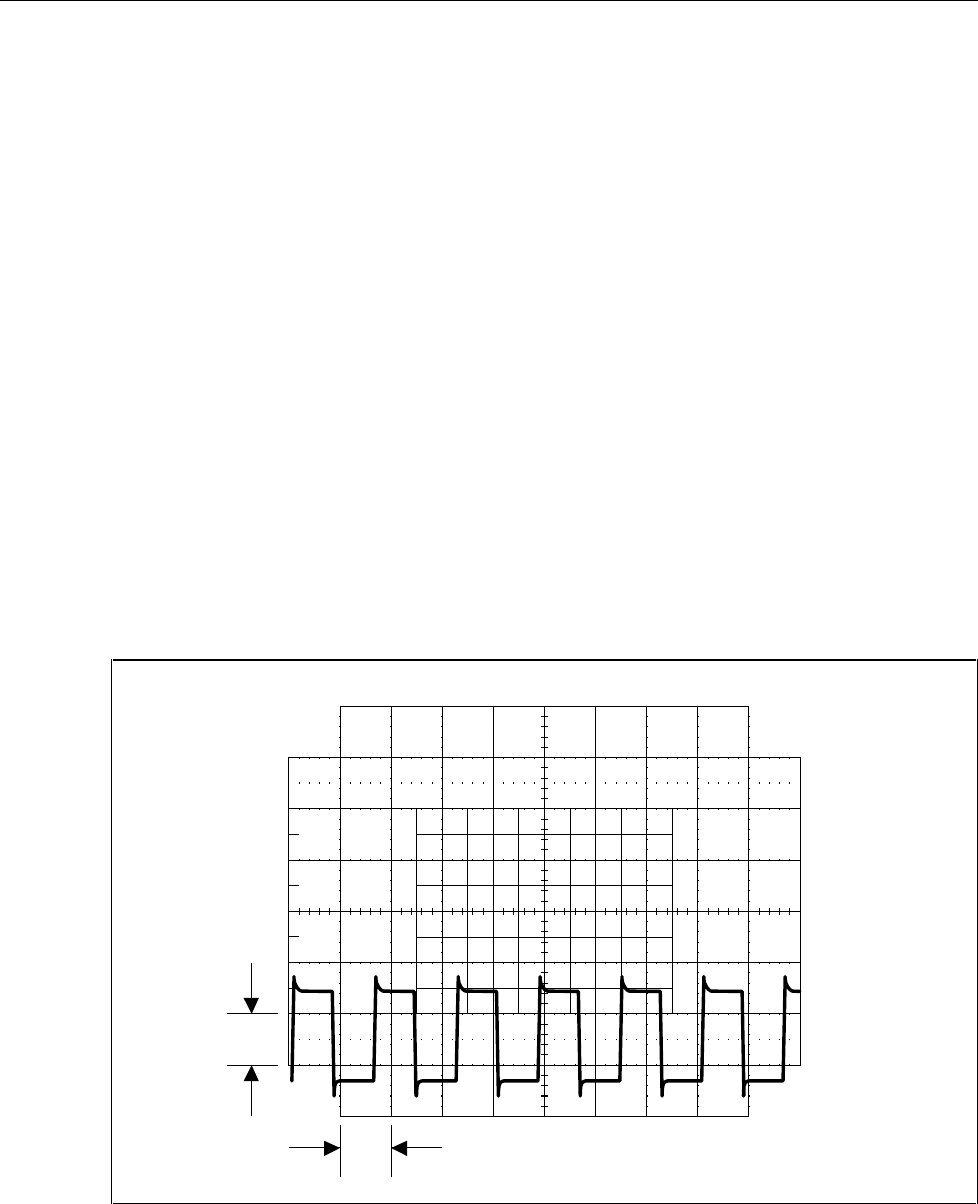
5700A/5720A Series II Calibrator
Service Manual
5-42
voltages of 3V, 1V, 300 mV, and 30 mV, all at 1 kHz, and verify the DMM read the
selected voltage ±5%. If a failure is detected, check K4-K8, Z1, and Z2. Next,
connect the supplied output cable and 50Ω terminator to the WIDEBAND connector
of the Calibrator front panel. Refer to the 5700A/5720A Series II Operators manual
and run Wideband Gain calibration. After the Wideband Gain calibration is complete
check the Wideband output at the end of the cable and 50Ω terminator at 3V, 1V,
300 mV, and 30 mV, all at 1 kHz, and verify the output is within 0.2%.
5-5. Troubleshooting the Wideband Oscillator Assembly (A6)
Proceed as follows to troubleshoot the Wideband Oscillator assembly (A5):
1. Remove the front and rear shields from the Wideband Oscillator assembly and place
it up on the extender card. Power up the Calibrator and call up the Wideband
function.
Note
All measurements are referenced to SCOM (TP16 or TP17) and all
Calibrator outputs are from the Wideband Option unless otherwise Noted.
2. Set the Calibrator to 1V at 1.2 MHz, operate. Connect an oscilloscope to TP10, set it
to 500 mV/div at 500 ns/div, and verify it displays a1.2 MHz signal similar to that
shown in Figure 5-1. Next, connect a frequency counter to TP10. Set the Calibrator
to 2 MHz, 5 MHz, 10 MHz, 20 MHz, and 30 MHz, verify that each frequency is
within 0.01% of the nominal. If a failure is detected, proceed with step 3 otherwise
skip to step 11.
1 V
10 ms
F5-1.EPS
Figure 5-1. Waveform at TP10
3. Check the 8 MHz reference. Set the Calibrator to 1V at 1.2 MHz operate. Connect an
oscilloscope to TP1 and verify it displays a 8 MHz signal similar to that shown in
Figure 5-2. If a failure is detected, first verify that control line WB ON/OFF* is a
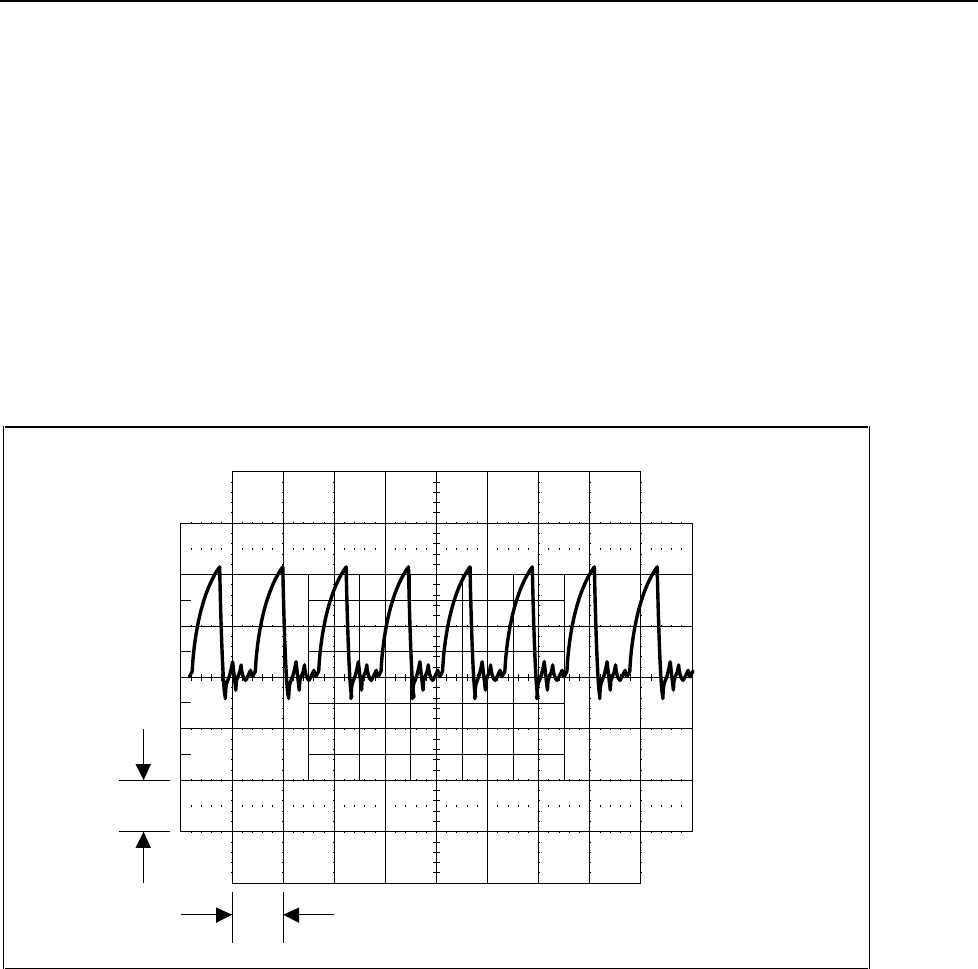
Troubleshooting
Component-level Troubleshooting
5
5-43
logic high by measuring U15 pin 5. If the signal is incorrect, the control line WB
ON/OFF* from the Wideband Output (A5) assembly is probably at fault. If the
control line is correct check U15A and associated components.
Note
The input CLK and CLK* is a low-level (400 mV p-p) signal generated by
the Regulator/Guard Crossing assembly.
4. Check the 4 MHz to 8 MHz feedback signal. Set the Calibrator to 1V at 1.2 MHz,
operate. Connect an oscilloscope to TP15 and verify it displays a 4.8 MHz signal
similar to that shown in Figure 5-3. Use a frequency counter and verify that the
frequency of this signal is 4.8 MHz ±0.01%. If a failure is detected, continue with
step 5; otherwise skip to step 10.
1 V
10 ms
F5-2.EPS
Figure 5-2. Waveform at TP1
5. Check the VCO Supply Voltage. Set the Calibrator to 1V at 1.2 MHz, operate. Using
a DMM measure the dc voltage at U3 pin 8 and verify it is -5V ±7%. If a failure is
detected, check Q2, Q3, U7, and associated components.
6. Check the VCO circuit. Power down the Calibrator, remove shorting header E6 from
the J6 pins, and connect an external variable dc reference(2V to 13V) to TP2. Power
up the Calibrator and set it for 1V at 1.2 Mhz, operate. Connect a frequency counter
to TP3. Vary the external dc reference from 2 to 12V and verify the frequency
counter reading changes from approximately 32 to 64 MHz. If a failure is detected,
check the VCO circuit containing U3, CR1, CR2, and associated components.
7. Check the dividers in U4 and U5. Power down the Calibrator, remove shorting
header E6 from the J6 pins, and connect an external variable dc reference (2 to 13V)
to TP2. Power up the Calibrator and set it for 1V at 1.2 MHz, operate. Connect a
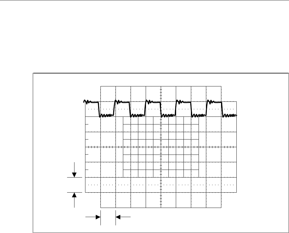
5700A/5720A Series II Calibrator
Service Manual
5-44
frequency counter to TP3 and adjust the external dc reference until the frequency
counter reads 64 MHz ±0.1%. Using the frequency counter, measure the frequency
at TP4 and verify it reads 32 MHz ±0.1%. If a failure is detected, check U4 and
associated components. Next, measure the frequency at pins 15, 13, 4, and 2 of U5
and verify that pin 15 measures 16 MHz ±0.1%, pin 13 measures 8 MHz ±0.1%, pin
4 measures 4 MHz ±0.1%, and pin 2 measures 2 MHz ±0.1%. If a failure is detected,
check U5 and associated components.
1 V
10 ms
F5-3.EPS
Figure 5-3. Waveform at TP15
8. Check the Synthesizer IC U1. Power down the Calibrator, remove shorting header
E6 from the J6 pins, and connect an external variable dc reference (2 to 13V) to TP2.
Power up the Calibrator and set it for 1V at 6 MHz, operate. Connect a frequency
counter to TP15 and adjust the external dc reference until the counter reads less than
6 MHz (~5.8MHz). Connect an oscilloscope to pin 15 of U1 and verify it displays a
signal similar to Figure 5-4. Next, adjust the external dc reference until the counter
reads more than 6 MHz (~6.2 MHz).Connect an oscilloscope to pin 14 of U1 and
verify it displays a signal similar to Figure 5-4. If a failure is detected, check U1 and
associated components.
9. Check the Amplifier Circuit. Power down the Calibrator, remove shorting header E6
from the J6 pins, and connect an external variable dc reference (2 to 13V) to TP2.
Power up the Calibrator and set it for 1V at 6 MHz, operate. Connect a frequency
counter to TP15 and adjust the external dc reference until the counter reads less than
6 MHz (~5.8 MHz). Connect an oscilloscope to pin 6 of U2 and verify it displays a
positive dc voltage. Next, adjust the external dc reference until the counter read more
than 6 MHz (~6.2 MHz) and verify the oscilloscope connected to pin 6 of U2
displays a negative dc voltage. If a failure is detected, check U2 and associated
components.

Troubleshooting
Component-level Troubleshooting
5
5-45
1 V
10 ms
F5-4.EPS
Figure 5-4. Waveform at Pins 14 and 15 of U1
Note
Power down the Calibrator, remove the external dc reference, and replace
shorting header E6 on the J6 pins before continuing.
10. Check the Multiplexer U6 and its control lines. Power up the Calibrator and it to 1V
at 1.2 MHz, operate. Connect a frequency counter to TP10 and measure the logic
levels of the control lines at pins 7, 9, and 10 of U6 using the data in Table 5-1
following table. Verify the logic levels are correct and the output frequency at TP10
is within 0.01%. If a failure is detected, check U6, U7, and associated components.
11. Check the Amplitude Control Amplifier circuit. Disconnect the cable between the
Wideband Oscillator assembly and Wideband Output assembly at J1 on the
Wideband Output assembly. Set the Calibrator to 1V at 1.2 MHz, operate. Connect
an oscilloscope set for ac coupling to pin 6 of U9 and verify it displays a signal
similar to Figure 5-5. If a failure is detected, check U9 and its associated
components in the Amplitude Control Amplifier circuit.
12. Check the X10 Wideband Amplifier circuit. Disconnect the cable between the
Wideband Oscillator assembly and Wideband Output assembly at J1 on the
Wideband Output assembly. Set the Calibrator to 1V at 1.2 MHz, operate. Connect
an oscilloscope set for ac coupling to TP13 and verify is displays a signal similar to
Figure 5-5, but approximately 10 times larger in amplitude. If a failure is detected,
check Q4, Q5, Q6, and associated components in the X10 Wideband Amplifier
circuit.
13. Check the Filter Select circuit. Disconnect the cable between the Wideband
Oscillator assembly and Wideband Output assembly at J1 on the Wideband Output
assembly. Set the Calibrator to 1V at 1.2 MHz, 2 Mhz, 4 MHz, 8 MHz, and 16 MHz.
At each frequency range verify the collector of the corresponding transistor in U13
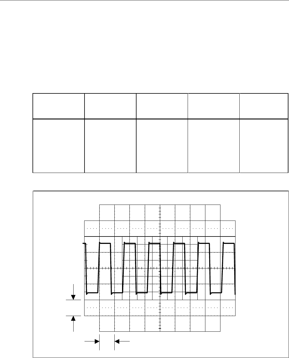
5700A/5720A Series II Calibrator
Service Manual
5-46
switches to a high(~+17V) level while all the others remain at a low (-11V) level. If
a failure is detected, check U8, U10, U11, and U13.
14. Check the Filters. Disconnect the cable between the Wideband Oscillator assembly
and Wideband Output assembly at J1 on the Wideband Output assembly. Set the
Calibrator to 1V at 1.2 MHz, 1.9 MHz, 2 MHz, 3.9 MHz, 4 MHz, 7.9 MHz, 8 MHz,
15.9 MHz, 16 MHz, and 30 Mhz. Connect an oscilloscope to TP14 and verify it
displays a distortion-free sine wave at each frequency. If a failure is detected, check
the corresponding Filter circuit.
Table 5-1. Verifying Multiplexer U66
5700A/5720A
Series II
Wideband Output
A
Pin 7
B
Pin 9
C
Pin 10
TP10
1-32 MHz
1.2 Mhz -5V -5V -5V 1.2 MHz
2.0 Mhz 0V -5V -5V 2.0 MHz
4.0 Mhz -5V 0V 0V 4.0 MHz
8.0 Mhz -5V -5V 0V 8.0 MHz
16.0 Mhz 0V 0V -5V 16.0 MHz
1 V
10 ms
F5-5.EPS
Figure 5-5. Waveform at Pin 6 of U9

Troubleshooting
Component-level Troubleshooting
5
5-47
5-6. Troubleshooting the Current/Hi-Res Assembly (A7)
The Current/Hi-Res assembly generates output current and contains the high-resolution
oscillator onto which the Oscillator Control assembly phase locks. Since these two
functions are independent except for their digital control, troubleshooting procedures for
each portion are presented separately.
5-7. Current Section
Proceed as follows to troubleshoot the current section of the Current/Hi-Res assembly
(A7):
1. In order to troubleshoot the Current generating circuitry it is necessary to break the
loop and use an external ac reference as the input source. Turn off the Calibrator and
cut jumper E1. Connect an external variable ac reference to TP19 (common to
TP20).
2. Place the Current/Hi-Res assembly on the analog reverse extender card and jumper
the Calibrator OUTPUT HI binding post to the OUTPUT LO binding post. Turn on
the Calibrator.
Note
All measurements are referenced to SCOM (TP20) unless otherwise
specified.
3. Check the Complimentary Drive Circuit. Set the Calibrator to 200 µA, standby. Set
the external ac reference to 7.0V at 1 kHz. Connect an oscilloscope to pin 11 of K2
and verify that it displays a signal similar to Figure 5-6. Connect the oscilloscope to
pin 6 of K2 and verify that it displays a signal similar to Figure 5-7. If a failure is
detected, check Q2, Q3, Q18, Q19, K2, and their associated components in the
Complimentary Drive Circuit.
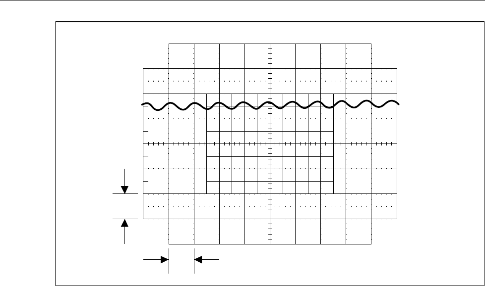
5700A/5720A Series II Calibrator
Service Manual
5-48
1 V
10 ms
F5-6.EPS
Figure 5-6. Waveform at Pin 11 of K2
4. Check the 220 µA range of the 220 µA/2.2 mA AMP circuit. Set the Calibrator to
200 µA, standby. Set the external ac reference to 6.4V(±0.1V) at 1 kHz. Using a
DMM, measure the ac voltage at the collector of Q4 and verify it is 2.0V ac ±10%. If
a failure is detected, first verify that the 10 kΩ shunt on HR2 is correct and that it is
connected to SCOM thought relays K5C, K5D, K10, K13 and the 1.2Ω load resistor
R14 as in Figure 5-8. If the shunt and output switching is correct check Q4, Q5, K3,
and the associated components in the 220 µA/2.2 mA AMP circuit.
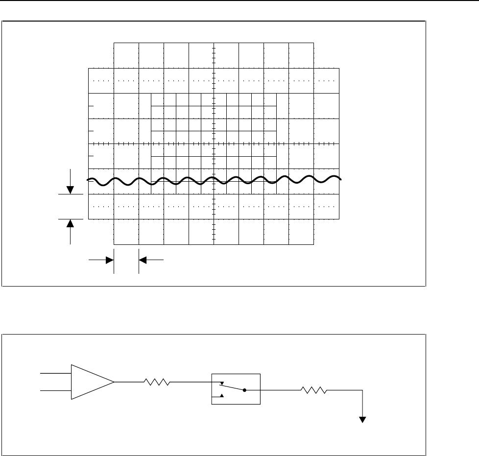
Troubleshooting
Component-level Troubleshooting
5
5-49
1 V
10 ms
F5-7.EPS
Figure 5-7. Waveform at Pin 6 of K2
10 k
HR2
SHUNT 1.2
R14
2V ac
±10% K5C, K5D,
K10, K13
SCOM
Ω
Ω
F5-8.EPS
Figure 5-8. Verifying the 220 µA Range of the 220 µA/2.2 mA Amp Circuit
5. Check the 2.2 mA Range of the 220 µA/2.2 mA AMP. Set the Calibrator to 2 mA,
standby. Set the external ac reference to 6.4V at 1 kHz. Measure the ac voltage at the
collector of Q4 with a DMM and verify it is 2.0V ac ±10%. If a failure is detected,
first verify the 1 kΩ shunt on HR2 is correct and it's connected to SCOM through
relays in K7A, K5D, K10, K13 and 1.2Ω load resistor R14 as shown in Figure 5-9. If
the shunt and output switching is correct check Q4, Q5, K3 and their associated
components in the 220 µA /2.2 mA AMP circuit.
6. Check the 22 mA Range of the 22 mA/220 mA AMP. Set the Calibrator to 20 mA,
standby. Set the external ac reference to 6.3V (±0.1V) at 1 kHz. Using a DMM
measure the ac voltage at the collector of Q6 and verify it is 2.0V ac ±10%. If a
failure is detected, first verify the 100Ω shunt on HR2 is correct and is connected to
SCOM through relays in K8C, K7A, K5D, K10, K13, and 1.2Ω load resistor R14, as
shown in Figure 5-10. If the shunt and output switching are correct, check Q6-Q13,
K4, and the associated components in the 22 mA/220 mA AMP circuit.
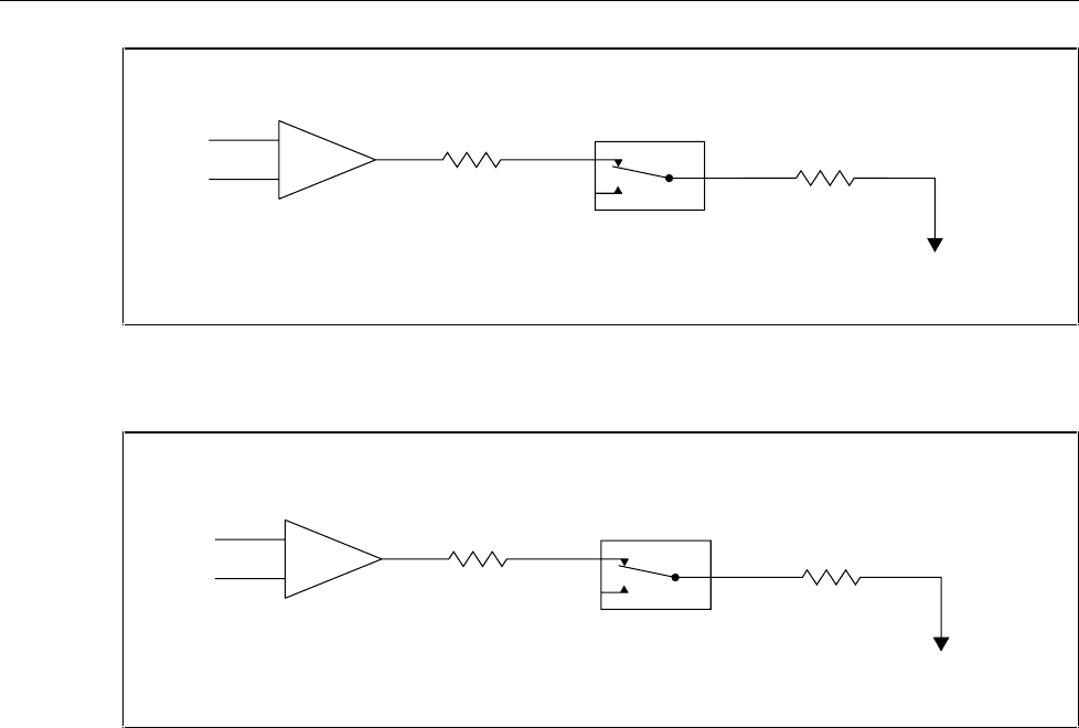
5700A/5720A Series II Calibrator
Service Manual
5-50
10 k
HR2
SHUNT 1.2
R14
2V ac
±10% K7C, K5D,
K10, K13
SCOM
Ω
Ω
F5-9.EPS
Figure 5-9. Verifying the 2.2 mA Range of the 220 µA /2.2 mA Amp Circuit
10 k
HR2
SHUNT 1.2
R14
2V ac
±10% K8C, K7A,
K5, K10, K13
SCOM
Ω
Ω
F5-10.EPS
Figure 5-10. Verifying the 22 mA Range of the 22 mA/220 mA Amp Circuit
7. Check the 220 mA Range of the 22 mA/220 mA AMP. Set the Calibrator to 200 mA,
standby. Set the external ac reference to 4.6V (±0.1V) at 1 kHz. Using a DMM
measure the ac voltage at the collector of Q6 and verify it is 2.0V ac ±10%. If a
failure first verify the 10Ω shunt on HR2 is correct and it's connected to SCOM
through relays in K9C, K8C, K7A, K5D, K10, K13, and 1.2Ω load resistor R14 as
shown in Figure 5-11. If the shunt and output switching are correct, check Q6-Q13,
K4, and the associated components in the 22 mA/220 mA AMP circuit.
8. Check the NEG. FB BUFFER. Set the Calibrator to 200 mA, standby. Set the
external ac reference to 4.6V at 1 kHz. Using a DMM measure the ac voltage at the
collector of Q6 and Note the reading. Next, measure the voltage at TP3 and verify it
is the same as the previous Noted reading ±0.01%. If a failure is detected, check U2,
K5A, K6A, K8A,K9A and the associated components.

Troubleshooting
Component-level Troubleshooting
5
5-51
10 k
HR2
SHUNT 1.2
R14
2V ac
±10% K9C, K8C,
K7A, K5D,
K10, K13 SCOM
Ω
Ω
F5-11.EPS
Figure 5-11. Verifying the 220 mA Range of the 22 mA/220 mA Amp Circuit
9. Check the POS. FB BUFFER. Set the Calibrator to 200 mA, standby. Set the
external ac reference to 4.6V at 1 kHz. Using a DMM measure the ac voltage at pin
5 of the HR2 resistor network and Note the reading. Next, measure the voltage at
TP4 and verify it is the same as the previous Noted reading ±0.1%. If a failure is
detected, check U3, K5B, K6B, K8B, K9B, and the associated components.
10. Check the I-GUARD BUFFER. Set the Calibrator to 200 mA, standby. Set the
external ac reference to 4.6V at 1 kHz. Measure the ac voltage at TP4 with a DMM
and Note the reading. Next, measure the voltage at U4 pin 6 and verify it is the same
as the previous Noted reading ±0.01%. If a failure is detected, check U4 and its
associated components.
Note
Replace or reconnect jumper E1 and remove the external ac reference
from the Current/Hi-Res assembly before continuing.
11. Check the Input Switching. Set the Calibrator to 2 mA dc, operate. Using a DMM,
measure the dc voltage at TP1 (common to TP2) and verify it is 20V dc ±0.25%.
Next, set the Calibrator to ac 2 mA at 1 kHz operate and measure the ac voltage at
TP1 and verify it is 20V ac ±25%. If a failure is detected, check K1, Q20-Q23, and
their appropriate drive circuitry.
12. Check the Z1 resistor network. Set the Calibrator to 2 mA dc, operate. Using a
DMM measure the dc voltage at pins 8 and 3 of Z1 and verify they are 1.818V dc
±0.35%. If a failure is detected, check Z1 and the HR2 hybrid.
13. Check the CURRENT/COMPLIANCE VOLTAGE MONITOR. Connect a 10Ω 1%
resistor across the Calibrator output and set the Calibrator to 200 mA at 1 kHz,
operate. Using a DMM measure the ac voltage at the OUT HI binding post and edit
the current output until it measures 2.0V ac ±0.01V. Next, measure the dc voltage at
TP9 and verify it is 0.238V dc ±10%. If a failure is detected, check U5, U6, and the
associated components in the CURRENT/COMPLIANCE VOLTAGE MONITOR
circuit.
14. Check the COMPLIANCE LIMITER. Connect a shorting jumper across the
Calibrator output and set the Calibrator to 2 mA dc, operate. Using a DMM monitor
the dc voltage at TP4. Remove the shorting jumper at the Calibrator output. The
voltage at TP4 should not exceed 11V ±5% before the Calibrator trips to standby. If
a failure is detected, check Q24, Q25, CR10, CR11, and the associated components
in the Compliance Limiter Circuit.
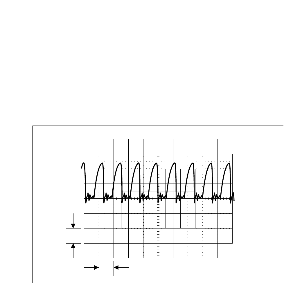
5700A/5720A Series II Calibrator
Service Manual
5-52
5-8. Hi-Res Oscillator Section
Proceed as follows to troubleshoot the Hi-Res Oscillator Section of the Current/Hi-Res
assembly (A7):
1. Remove the four small shields (two on each side) and place the Current/Hi-Res
assembly on the analog reverse extender card. Power up the Calibrator.
Note
All measurements are referenced to LHCOM (TP18).
2. Check the 8 MHz reference. Set the Calibrator to 2V at 1 kHz, operate. Connect an
oscilloscope to U13 pin 4 and verify it displays a 8 Mhz signal similar to that shown
in Figure 5-12. If a failure is detected, first verify that control line HI-RES ON/OFF
is a logic low by measuring U15 pin 12. If not U7 is probably at fault. If this control
line is correct check U13 and its associated components.
1 V
10 ms
F5-12.EPS
Figure 5-12. Waveform at Pin 4 of U13
Note
The input CLK and CLK* is a low level (400 mV p-p) signal generated by
the Regulator/Guard Crossing assembly.
3. Check the 2 MHZ REF. Set the Calibrator to 2V at 1 kHz, operate. Connect an
oscilloscope to TP12 and verify it displays a 2 MHz signal similar to that shown in
Figure 5-13. If a failure is detected, check U14A and U14B.
4. Check the 6-12 MHZ signal. Set the Calibrator to 2V at 1 kHz, operate. Connect an
oscilloscope to TP13 and verify it displays a 10 Mhz signal similar to that shown in
Figure 5-14. Also measure the frequency of this signal using a frequency counter and
verify it is within 9.999 MHz to 10.001 MHz. If a failure is detected, with either test
continue on as follows. If the signal and frequency are correct, skip to step 9.
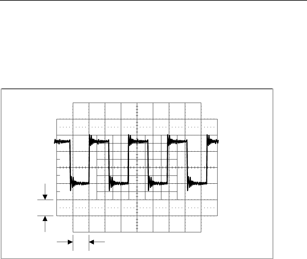
Troubleshooting
Component-level Troubleshooting
5
5-53
5. Check VCO Supply Voltage. Set the Calibrator to 2V at 1 kHz, operate. Using a
DMM measure the voltage at U19 pin 8 and verify it is -5.25V±7%. If a failure is
detected, check U18A, Q15, VR3, and associated components.
6. Check the VCO circuit. Power down the Calibrator, cut jumper E2 and connect an
external variable dc reference (2 to 12V) to TP11 (common to TP18). Power up the
Calibrator and set it for 2V at 1 kHz. Connect a frequency counter to TP13. Vary the
external dc reference from 2 to 12V and verify the frequency counter reading
changes from approximately 6 MHz to 12 MHz.
1 V
10 ms
F5-13.EPS
Figure 5-13. Waveform at TP12
Note
The voltage-to-frequency ratio is not important. It is only necessary to
verify that a change in voltage causes a change in oscillation frequency. If
a failure is detected check U19, CR9, and associated components in the
VCO circuit.
7. Check the PHASE DET/DIVIDERS. Power down the Calibrator, cut jumper E2 and
connect an external variable dc reference (2 to 12V) to TP11 (common to TP18).
Power up the Calibrator and set it for 2V at 1 kHz. Connect a frequency counter to
TP13 and adjust the external dc reference so the frequency counter reads less than 10
MHz (~9.8 MHz). Using an oscilloscope, verify that U16 pin 15 (0R) is pulsing and
U16 pin 14 (0V) is a logic high. Next, adjust the external dc reference so the
frequency counter reads greater than 10 MHz (~10.2 MHz). Using an oscilloscope,
verify that U16 pin 14 (0V) is pulsing and U16 pin 15 (0R) is a logic high. If a
failure is detected, U16 and/or its digital control is probably at fault.
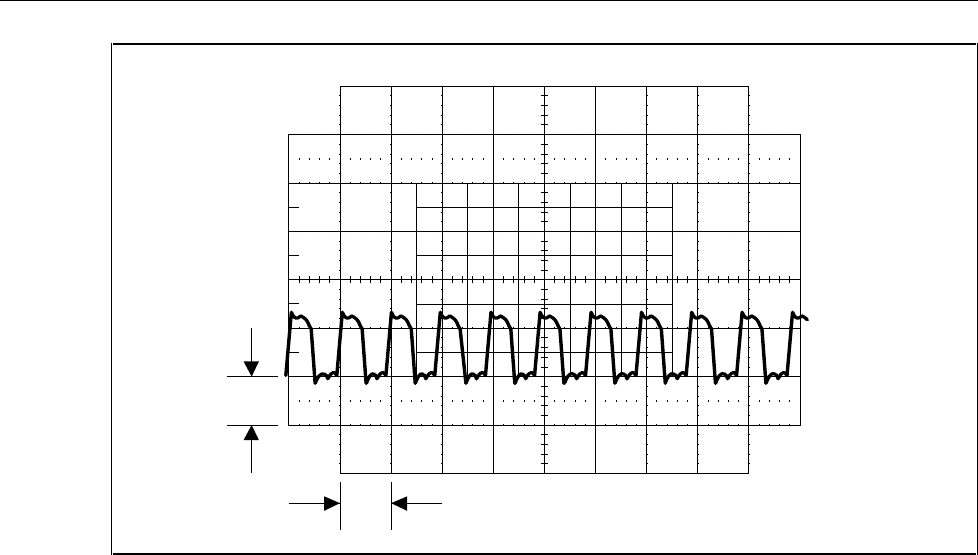
5700A/5720A Series II Calibrator
Service Manual
5-54
1 V
10 ms
F5-14.EPS
Figure 5-14. Waveform at TP13
8. Check the LOOP FILTER circuit. Power down the Calibrator, cut jumper E2 and
connect an external variable dc reference (2 to 12V) to TP11(common to TP18).
Power up the Calibrator and set it for 2V at 1 kHz. Connect a frequency counter to
TP13 and adjust the external dc reference so the frequency counter read less than 10
MHz (~9.8 MHz).Connect an oscilloscope to U20 pin 7 and verify it displays a
positive dc voltage. Next, change the dc reference so the frequency counter reads
greater than 10 MHz (~10.2 MHz). At this time U20 pin 7 should be a negative dc
voltage. If a failure is detected, check U20A, U20B, and associated components in
the LOOP FILTER circuit. Reconnect jumper E2 before continuing.
9. Check the 5-500K Divider. Connect a frequency counter to U21 pin 5. Set the
Calibrator to 2V at 1 MHz, 500 kHz, 200 kHz, 140 kHz, 100 kHz, and 50 kHz. At
each output frequency verify the frequency counter displays the same as selected
±0.01%. Next, connect the frequency counter to U21 pin 9. Set the Calibrator to 2V
at 2 kHz, 120 Hz, and 10 Hz. At each output frequency verify the frequency counter
displays the same as the selected ±0.01%. If a failure is detected, check U17 and
U21.
10. Check the Output Switching. Connect an oscilloscope and frequency counter to
TP16. Set the Calibrator for 2V at 1 kHz, operate, and verify the oscilloscope
displays a signal similar to Figure 5-15, and the frequency counter reads 1 kHz
±0.01%. Next, set the Calibrator for 2V at 100 kHz and verify the frequency counter
reads 100 kHz ±0.01%. If a failure is detected, check U18B, C, D, U15C, Q16, and
associated components.
5-9. Troubleshooting the Switch Matrix Assembly (A8)
Proceed as follows to troubleshoot the Switch Matrix assembly (A8):
1. The primary function of the Switch Matrix assembly is to connect the output from
the various assemblies within the Calibrator to the output binding posts via the
Motherboard relays. All relays on the Switch Matrix assembly are latching type.
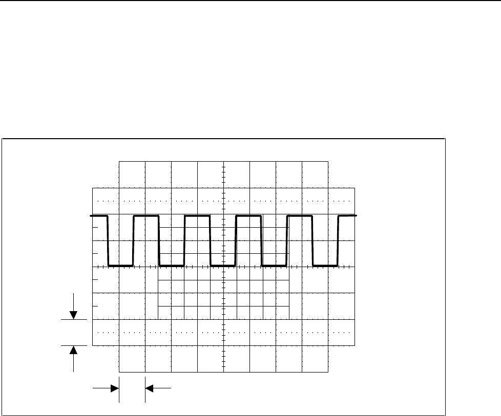
Troubleshooting
Component-level Troubleshooting
5
5-55
These relays are latched in the set or reset position and remain in that position even
after power has been removed. To troubleshoot the signal path through the Switch
Matrix assembly simply set the Calibrator to the function in which a problem is
detected and then turn off the Calibrator. Now remove the Switch Matrix from the
instrument and, using an ohmmeter, check the signal path by using the relay chart in
the schematic section. Check individual relays by connecting an external power
supply (a typical 9V battery works well) across the set coil to place the relay in the
set position or the reset coil to place the relay in the reset position.
1 V
10 ms
F5-15.EPS
Figure 5-15. Waveform at TP16
2. Check the Motherboard relay RLY+V supply voltage. Set the Calibrator to 10V dc,
operate. Connect an oscilloscope to RLY+V (common to TP9),which is at the
cathode of CR2, and verify it is 4.5V ±0.5V. Now verify that each time the EX SNS
key is pressed the voltage at RLY+V momentarily jumps to 7.5V ±1.2V. If a failure
is detected, check the control line PC5, U17, Q1, Q2, and associated components.
3. Check the Motherboard relay control lines. Motherboard relays K1-K10 are
controlled by U13 on the Switch Matrix assembly. If aMotherboard relay problem is
suspected, verify U13 by using the relay chart in the Switch Matrix schematic
section and checking for correct logic levels at its output.
4. Check the 2.2V Range Attenuator. Set the Calibrator to 2V dc, operate. Using a
DMM measure the dc voltage at TP2 (common to TP8) and verify it is 2V ±6 mV.
Note
This 2V can be as much as ±0.12V if the DAC assembly is uncalibrated. If
a failure is detected, check K1, K2, and the 5:1 divider part of the HR1
resistor network.
5. Check the 2.2V Range Amplifier. Set the Calibrator to 2V dc, operate. Using a
DMM measure the dc voltage at TP4 (common to TP8) and verify it is 2V ±6 mV.

5700A/5720A Series II Calibrator
Service Manual
5-56
Note
This 2V can be as much as ±0.12V if the DAC assembly is uncalibrated. If
a failure is detected, check the HR1 hybrid, U19, Q4, and associated
components.
6. Check the mV Dividers. Set the Calibrator to 200 mV at 1 kHz, operate. Using a
DMM measure the ac voltage at the cathode of CR6 (common to OUTPUT LO
binding post) and verify it is 200 mV ±1%. Next, set the Calibrator to 20 mV at 1
kHz operate and again measure the ac voltage at the cathode of CR6. Verify it is 20
mV ±1%. If a failure is detected, check the resistive dividers in the HR1 resistor
network and the associated relays.
5-10. Troubleshooting the Ohms Cal Assembly (A9)
Proceed as follows to troubleshoot the Ohms Cal assembly (A9):
1. The Ohms Cal assembly contains the two-wire lead drop compensation circuit,
calibration circuitry, the 1Ω, 1.9Ω, and short resistance values. All relays on the
Ohms Cal assembly are latching type. These relays are put in the set or reset position
and they remain in that position even after power has been removed. To troubleshoot
the path through the relays simply set the Calibrator to the function in which
problem is detected and then turn off the Calibrator. The relays remain in either the
set or reset position. Check individual relays by connecting an external power supply
(a typical 9V battery works well) across the set coil to place the relay in the set
position or the reset coil to place the relay in the reset position. Remove the rear
shield from the assembly and put it up on the extender card. Power up the Calibrator
and continue as follows.
2. Check the 1Ω, 1.9Ω, and short. Connect a four-terminal ohmmeter(such as a Fluke
Model 8505A) to the Ohms Cal assembly as follows. Connect 8505A IN HI to TP1,
8505A IN LO to TP 2, 8505A SENSE HI to TP5, 8505A SENSE LO to TP6. Set the
Calibrator to 1Ω, operate, EXT SNS, and verify the ohmmeter reads 1Ω ±0.1%. If a
failure is detected, check relays K4, K5, K6, and the four wire-wound resistors in
R41. Set the Calibrator to 1.9Ω, operate, EXT SNS, and verify the ohmmeter reads
1.9Ω ±0.1%. If a failure is detected, check relays K4, K5, K30, and the two wire-
wound resistors in R42. Set the Calibrator to 0Ω and verify the ohmmeter reads 0Ω
±0.1%. If a failure is detected, check relays K7 and K8.
5-11. Two-wire Compensation Circuit
Proceed as follows to troubleshoot the two-wire compensation circuit:
1. Check the +8A and -8A power supply for the two-wire comp. circuit. Set the
Calibrator to 100Ω, operate, and turn the two-wire comp on. Using a DMM measure
the dc voltage at TP8 (common to TP7) and verify it is +8.2V ±5%. Next, measure
the dc voltage at TP9 (common to TP7) and verify it is -8.2V ±5%. If these supply
voltages are correct skip to step 2. If a failure is detected, first connect an
oscilloscope to pin 16 of U6 with the scope common connected to pin 13 of U6. Set
the oscilloscope to 5V/div at 10 us/div and verify it displays a waveform similar the
Figure 5-16. If a failure is detected, check U6, Q5, Q6, Control line PB7, and
associated components. If this signal is correct then check T1, CR1, CR2, CR9,
CR10, VR1, VR2, and associated components.
2. Set the Calibrator to 100Ω, operate, INT SNS, and 2-Wire Comp ON. Connect a
Fluke 8505A DMM, set to the 100Ω range, across the Calibrator OUTPUT HI and
OUTPUT LO binding posts. The current from the DMM should be 10 mA. Using
another DMM measure the dc voltage between pins 4 and 5 of U7 and verify it is
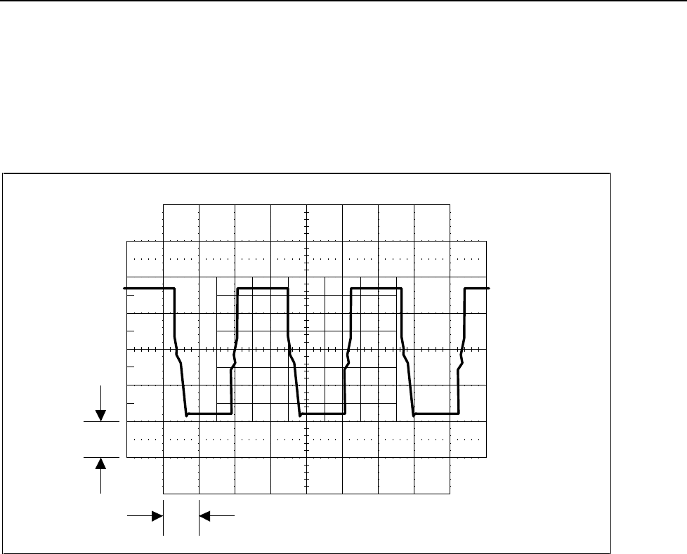
Troubleshooting
Component-level Troubleshooting
5
5-57
less than 4 µV. If a failure is detected check U7, U8, and associated components.
Using a DMM measure the dc voltage across the 500Ω resistor in Z2 by connecting
the DMM HI to TP18 and the DMM LO to TP17. Note this voltage which should be
around 5.0V. Next, measure the voltage across the 1 kΩ resistor in Z2 by connecting
the DMM HI to TP16 and the DMM LO to TP6. The voltage should be double and
opposite polarity (gain = -2)of that previously measured (about -10V). If a failure is
detected check U9, U10, and associated components.
1 V
10 ms
F5-16.EPS
Figure 5-16. Waveform at Pin 13 of U6
5-12. Troubleshooting the Ohms Main Assembly (A10)
Proceed as follows to troubleshoot the Ohms Main assembly (A10):
1. MΩ resistor in R1. All of the fixed values of resistance, available from the
Calibrator, reside on the Ohms Main assembly except the 1.9Ω, 1.0Ω, and short. The
fixed values of resistance from 10Ω to 100 MΩ are connected to the Calibrator
output binding posts through relays on the Ohms Main, Ohms Cal, and Motherboard
assemblies. The Ohms Main assembly is checked by verifying each fixed value of
resistance and the relay path to INT OUT HI, INT SENSE HI, OHMS OUT LO, and
OHMS SENSE LO. Place the Ohms Main assembly on the extender card, power up
the Calibrator, and continue as follows.
2. Connect a four-terminal ohmmeter (such as the Fluke Model 8505A) to the Ohms
Main assembly as follows. Connect 8505A IN HI to TP4, 8505A IN LO to TP3,
8505A SENSE HI to TP5, and 8505A SENSE LO to TP2. Set the Calibrator to 10Ω,
operate, EXT SNS and verify the ohmmeter reads 10Ω ±0.07%. If a failure is
detected, turn off the Calibrator and remove the Ohms Main assembly from the
extender card. Use the schematic and the relay chart to check the connection from
the test points to the 10Ω resistance.

5700A/5720A Series II Calibrator
Service Manual
5-58
Note
The connection from the test points to the resistance values is through
latching type relays for all resistances except 10M, 19M, and 100 M
Ω
values. These relays are put in the set or reset position and remain in that
position even after power has been removed. To troubleshoot the path
through the relays, simply set the Calibrator to the function in which a
problem is detected and then turn off the Calibrator. The relays remain in
either the set or reset position. Check individual relays by connecting an
external power supply (a typical 9V battery works well) across the set coil
to place the relay in the set position or the reset coil to place the relay in
the reset position.
3. Repeat step 2 for the resistances in Table 5-2 and verify they are within the specified
tolerance.
Table 5-2. Ohms Main Resistance Tolerance
Resistance Tolerance
19Ω+/-0.07%
100Ω+/-0.03%
190Ω+/-0.03%
1 kΩ+/-0.03%
1.9 kΩ+/-0.03%
4. Check the 100 MΩ resistance. Set up the ohmmeter for a two wire resistance
measurement and connect IN HI to TP4 and IN LO to TP3. Set the Calibrator to 100
MΩ, operate, INT SNS, and verify the ohmmeter reads 100 MΩ ±5.0%. If a failure
is detected, check relay K5 and90.
5-13. Troubleshooting the DAC Assembly (A11)
Proceed as follows to troubleshoot the DAC assembly (A11):
1. Remove the front and back shields and place the DAC assembly on the extender
card. Power up the Calibrator.
2. Check the 13V reference. Connect DMM to TP2 (common to TP3). The voltage
should be between +13 and +14V and very stable. (Some drift may be seen while the
assembly is warming up.) If the 13V reference is faulty, check the power supply
voltages to the HR5 Reference Hybrid. If all the supplies are correct, the HR5
Reference Hybrid is probably at fault.
3. Check CH1 SHUNT. Connect an oscilloscope probe to TP6 (with common
connected to TP3). Set the oscilloscope to 2V/div at 2 ms/div and verify it displays
pulses as shown in Figure 5-17. If the displayed signal is incorrect, skip to Duty
Cycle Control Circuit.
4. Check CH1 SERIES B. Connect an oscilloscope to TP4 (common to TP3).Set the
oscilloscope to 10V/div at 2 ms/div and verify it displays pulses as shown in Figure
5-18. Next, set the Calibrator to 6.5V dc, operate. Verify the oscilloscope displays
pulses with approximately 50% duty cycle as shown in Figure 5-19. If either of these
displayed signals are incorrect, skip to Duty Cycle Control Circuit.
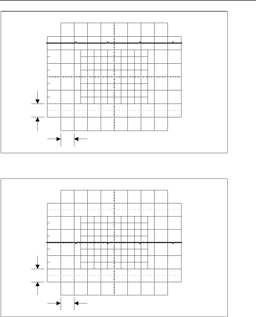
Troubleshooting
Component-level Troubleshooting
5
5-59
1 V
10 ms
F5-17.EPS
Figure 5-17. Waveform at TP6
1 V
10 ms
F5-18.EPS
Figure 5-18. Waveform at TP4, Calibrator Set to 0V
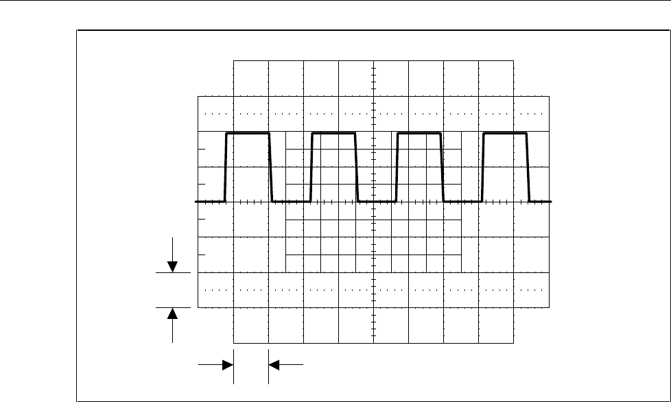
5700A/5720A Series II Calibrator
Service Manual
5-60
1 V
10 ms
F5-19.EPS
Figure 5-19. Waveform at TP4, Calibrator Set to 6.5V
5. Check CH2 FILTER INPUT. Connect an oscilloscope probe to TP7 (common to
TP3). Set the Calibrator to 6.5V dc, operate. Set the oscilloscope to 2V/div at 2
ms/div. Verify the oscilloscope displays pulses similar to those shown in Figure 5-
20.
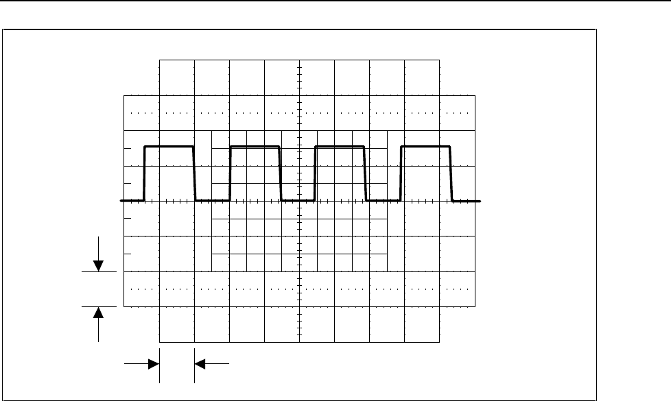
Troubleshooting
Component-level Troubleshooting
5
5-61
1 V
10 ms
F5-20.EPS
Figure 5-20. Waveform at TP7
Note
The duty cycle may differ from this figure. Using the Calibrator edit knob,
vary the second LSD of the Calibrator output display and verify that the
duty cycle of the signal at TP7 changes. If either of these displayed signals
are incorrect, skip to Duty Cycle Control Circuit.
6. Check the SERIES LINEARITY CONTROL CIRCUIT. Using a DMM measure the
voltage at U38 pin 6 (common to TP3). The voltage should be +23.0 to +26.4V. If
this voltage is incorrect, check U38 and Z2.
7. Check the NEG. OFFSET CIRCUIT. Using a DMM measure the voltage at U2 pin 1
(common to TP3). The voltage should be -13 to -14V which is the reference voltage
inverted. If this voltage is incorrect, check U2A and part of the HR6 resistor
network.
8. Connect an oscilloscope to TP5 (common to TP3), and set the Calibrator to 6.5V dc,
operate. Set the oscilloscope to 5V/div at 2 ms/div and verify the signal is similar to
that shown in Figure 5-21. If this signal is incorrect, check Q4, Q5, Q6, and Q7.
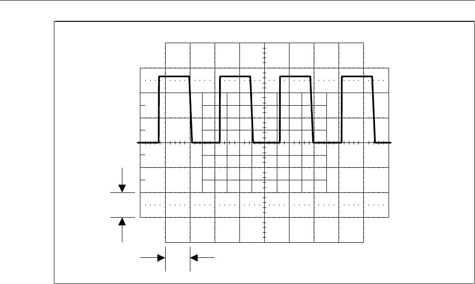
5700A/5720A Series II Calibrator
Service Manual
5-62
1 V
10 ms
F5-21.EPS
Figure 5-21. Waveform at TP5
9. Check the FILTER INPUT. Set the Calibrator to 6.5V dc, operate. Measure the
voltage with a DMM at TP1 (common to TP3 on the main board) on the DAC Filter
SIP assembly (A11A1). It should be a nominal +6.5V dc(±0.1V for an uncalibrated
instrument), free of distortion, and stable. If a failure is detected, check the DAC
Filter SIP assembly.
10. Check the DC AMP HYBRID. Set the Calibrator to 10V dc, operate. Measure the
voltage with a DMM at pin 18 (common to TP3) of the HR6 DC AMP HYBRID. It
should be a nominal +10V dc (±0.25V for an uncalibrated instrument), free of
distortion, and stable. If a failure is detected, check the HR6 Hybrid assembly and its
heater control circuit.
11. Check the OUTPUT BUFFER circuit. Set the Calibrator to 10V dc, operate. Measure
the voltage with a DMM at L10 (common to TP3). It should be a nominal +10V dc
(±0.25V for an uncalibrated instrument), free of distortion, and stable. If a failure is
detected, check U5 and its associated components.
12. Check the DAC OUTPUT SWITCHING. Set the Calibrator to 10V dc, operate.
Measure the DAC output voltage with a DMM a TP8 (common to TP12).It should
be a nominal +10V dc (±0.25V for an uncalibrated instrument). Set the Calibrator to
-10V dc, operate. Again check the voltage at TP8 (common to TP12). It should be a
nominal -10V dc(±0.25V for an uncalibrated instrument). If either of these voltages
are incorrect, check the output switching relays K1, K2, K8, and their drive circuitry.
13. Check the RANGE SELECT control line. Set the Calibrator to 10V dc, operate.
Using a DMM measure the RANGE SELECT control line at U37 pin 7 (common to
TP3). It should be -16 to -19V dc. Set the Calibrator to 20V operate and again
measure the RANGE SELECT control line for +4.0V to +11V. If either of these
measurements are incorrect, check U37, U8B, U8C, and their associated
components.

Troubleshooting
Component-level Troubleshooting
5
5-63
14. Check the DAC 20V Range. Set the Calibrator to 20V dc, operate. Using a DMM
measure the DAC output voltage at TP8 (common to TP3). It should be a nominal
20V dc (±0.5V for an uncalibrated instrument). If a failure is detected, check Q14,
Q15, Q18, Q19, Q20, Q21, and their associated components.
15. Check the SHUNT LINEARITY CONTROL CIRCUIT. Set the Calibrator to 10V
dc, operate. Measure the voltage with a DMM at U2 pin 7 (common to TP3).It
should be a nominal -10V dc (±0.35V for an uncalibrated instrument and ±0.1V for a
calibrated instrument). Set the Calibrator to 20V dc, operate, and again measure the
voltage at U2B pin 7. It should still be the nominal -10V dc within the same
tolerance. If either of these voltages are incorrect, check U2B, Q22, and the
associated 80 kΩ resistors in the HR6 Hybrid assembly.
16. Check the SENSE HI CURRENT CANCELLATION CIRCUIT. Set the Calibrator
to 10V dc, operate. Measure the voltage with a DMM at TP8 (common to TP3) and
Note the reading. Next, measure the output high binding post of the Calibrator
(common to TP3). It should be the same as the Noted reading ±10 ppm. If a failure is
detected, check U1A and associated components in the Sense Hi Current
Cancellation Circuit.
5-14. Duty-cycle Control Circuit
Proceed as follows to troubleshoot the duty-cycle control circuit:
1. Check the 8 MHz clock for U6. Connect an oscilloscope to U6 pin 10(common to
TP1). Set the oscilloscope for 2V/div at 100 ns/div and verify the display shows an 8
MHz clock similar to that shown in Figure 5-22. If a failure is detected, check U7
and its associated components. The input signal (CLK and CLK*) to U7 is a low-
level(400 mV p-p) 8 MHz clock generated by the Regulator/Guard Crossing
assembly.
2. Check OUT1 from U6. Connect an oscilloscope to U6 pin 16 (common to TP1). Set
the Calibrator to 6.5V dc, operate, and set the oscilloscope to 2V/div at 2 ms/div.
The oscilloscope should display a TTL-level square wave with approximately a 50%
duty cycle. If a failure is detected, check U6 and all its control lines.
3. Check OUT2 from U6. Connect an oscilloscope to U6 pin 20 (common to TP1). Set
the Calibrator to 6.5V dc, operate, and the oscilloscope to 2V/div at 2 ms/div. The
oscilloscope should display a TTL level square wave. If a failure is detected, U6 is
probably at fault.
4. Check CH1 FLOATING. Connect an oscilloscope to U13 pin 6 (common to TP1).
Set the Calibrator to 6.5V dc, operate, and the oscilloscope to 2V/div at 2 ms/div.
The oscilloscope should display a TTL level signal similar to Figure 5-23. If a
failure is detected, check U13 and its associated components.
5. Check the Clock to U14. Connect an oscilloscope to U10 pin 4 (common= TP3) and
set it for 2V/div at 100 ns/div. Verify it displays a 8 MHz clock similar to Figure 5-
24. If a failure is detected, check U10 and its associated components.
6. Check the Watchdog Clock. Connect an oscilloscope to U14 pin 8(common to TP3)
and verify it displays a TTL level 4 MHz clock. If a failure is detected, check U14.
7. Check the Watchdog Timer. Connect an oscilloscope to U15 pin 13(common to
TP3) and verify it displays a constant logic high. If a failure is detected, check U15
and associated components.
8. Check the Q1 and Q1* output of U14. Connect an oscilloscope to U14 pin 5
(common to TP3). Set the Calibrator to 6.5V dc, operate, and set the oscilloscope to
2V/div at 2 ms/div. The oscilloscope should display a TTL-level square wave with
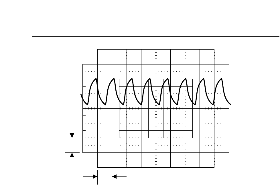
5700A/5720A Series II Calibrator
Service Manual
5-64
approximately a 50% duty cycle. Connect the oscilloscope to pin 6 of U14 and verify
it to be the compliment signal. If either signal is incorrect, U14 is probably at fault.
1 V
10 ms
F5-22.EPS
Figure 5-22. Waveform at Pin 10 of U6
9. Check CH1 SHUNT. Connect an oscilloscope to TP6 (common to TP3). Set the
Calibrator to 6.5V dc, operate, and set the oscilloscope to 2V/div at 2 ms/div. The
oscilloscope should display a signal similar to Figure 5-25. If a failure is detected,
check Q35 and its associated components.
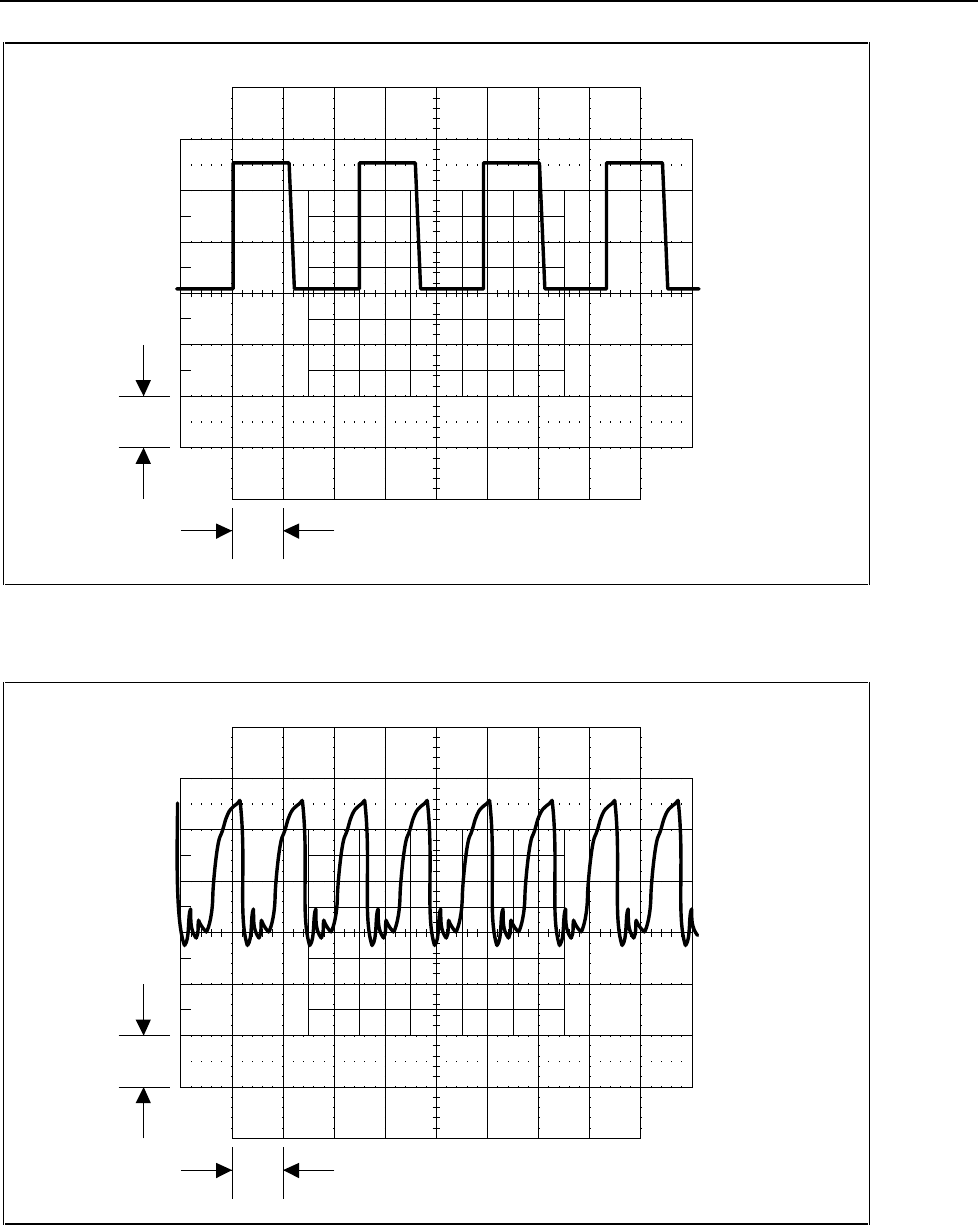
Troubleshooting
Component-level Troubleshooting
5
5-65
1 V
10 ms
F5-23.EPS
Figure 5-23. Waveform at Pin 6 of U13
1 V
10 ms
F5-24.EPS
Figure 5-24. Waveform at Pin 4 of U10
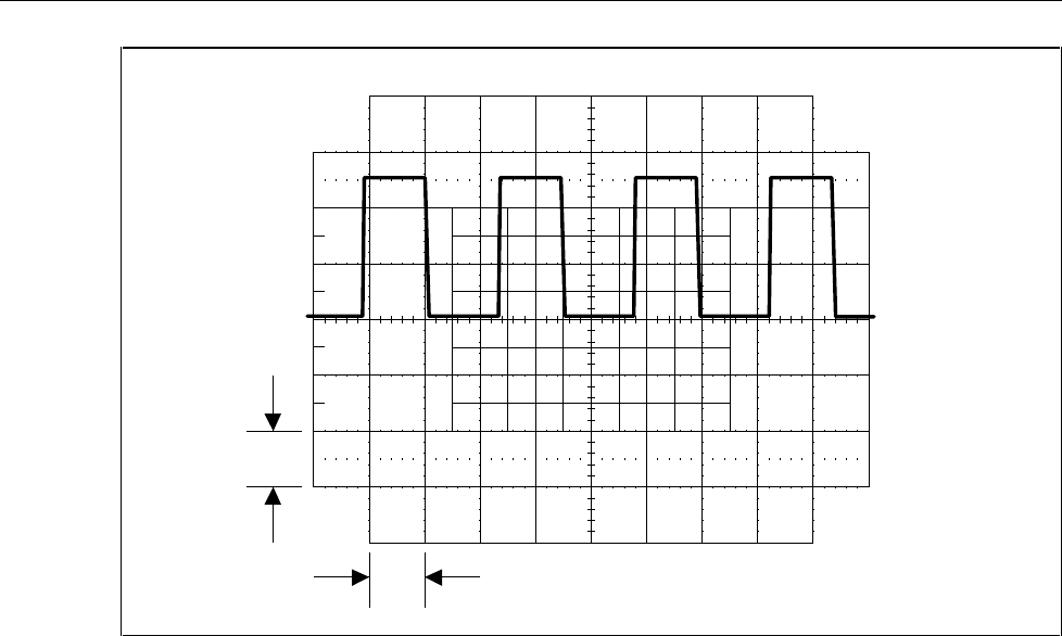
5700A/5720A Series II Calibrator
Service Manual
5-66
1 V
10 ms
F5-25.EPS
Figure 5-25. Waveform at TP6
10. Check CH1 SERIES B. Connect an oscilloscope to TP4 (common to TP3).Set the
Calibrator to 6.5V dc, operate, and the oscilloscope to 10V/div at 2 ms/div. The
oscilloscope should display a signal similar to previously shown Figure 5-19. If a
failure is detected, check Q33, Q34, and their associated components.
11. Check CH2 FLOATING. Connect an oscilloscope to U12 pin 7 (common to TP3)
and set it to 10V/div at 2 ms/div. Verify it displays a signal similar to Figure 5-26.
Note
The duty cycle may differ from Figure 5-26. At this time just verify the
amplitude and a sharp rise and fall time. If a failure is detected, check U12
and its associated components.
12. Check 3V reference. Using a DMM measure the voltage at U11 pin 3(common to
TP3) for a nominal 3V dc. If this voltage is incorrect check U1B and the associated
resistors on the HR5 Hybrid assembly.
13. Check CH2 FILTER INPUT. Connect an oscilloscope to TP7 (common to TP3) and
set it to 2V/div at 2 ms/div. Verify it displays a signal similar to the previously
shown Figure 5-20.
Note
The duty cycle may differ from Figure 5-20. If a failure is detected, check
U11, Q30, Q31, Q32, and their associated components.
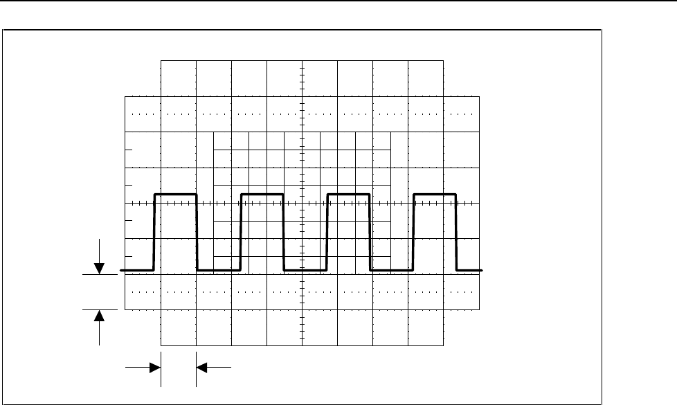
Troubleshooting
Component-level Troubleshooting
5
5-67
1 V
10 ms
F5-26.EPS
Figure 5-26. Waveform at Pin 7 of U12
5-15. ADC Circuit
Proceed as follows to troubleshoot the ADC circuit:
1. Check the ADC INPUT select circuit. Set the Calibrator to 10V dc, operate. Verify
that the voltage at U23 pin 7 (common to TP12) is 0.45V±7%. If this voltage is
incorrect, check U23 and its control lines. At this time DAC HI DIAG is divided by
R79 and R84 (0.45V)and selected by control line DAC DIAG SEL.
2. Check the ADC INPUT. Set the Calibrator to 10V dc, operate. Verify that the
voltage at U25 pin 22 (common to TP12) is 0.45V±7%. If this voltage is incorrect,
check U24 and its associated components.
3. Check the buffered DAC LO DIAG. Set the Calibrator to standby. Verify that the
voltage at U22 pin 6 (common to TP1) is 0V±11 mV. If this voltage is incorrect,
check U22 and associated components.
4. Check the ADC +7.5V supply. Set the Calibrator to standby. Verify that the voltage
at U25 pin 16 (common to TP1) is 7.5±0.5V. If this voltage is incorrect, check VR27
and R77.
5. Check the ADC -8.2V supply. Set the Calibrator to standby. Verify that the voltage
at U25 pin 17 (common to TP1) is -8.2±0.5V. If this voltage is incorrect, check
VR28 and R94.
6. Check the BUFFERED ADC COM. Set the Calibrator to standby. Verify that the
voltage at U26 pin 7 (common to TP12) is 0V±600 mV. If this voltage is incorrect,
check U20B, U26A, and associated components.
7. Check the ADC -6.4V Reference. Verify that the voltage at the anode of VR29
(common to TP12) is -6.4±0.2V. If this voltage is incorrect, check VR29, VR30,
U20B, U26A, and associated components.

5700A/5720A Series II Calibrator
Service Manual
5-68
8. Check the ADC +6.4V Reference. Verify that the voltage at U27 pin 1(common to
TP12) is 6.4±0.2V. If this voltage is incorrect, check U27B and associated
components.
9. Check the ADC SAMPLE/HOLD +BOOTSTRAP supply. Set the Calibrator to
standby. Verify that the voltage at U29 pin 7 (common to TP12) is between 5.4 and
8.2V. If this voltage is incorrect, check U29, Q56, Q57, VR31-VR34, and associated
components.
10. Check the ADC SAMPLE/HOLD -BOOTSTRAP supply. Set the Calibrator to
standby. Verify that the voltage at U29 pin 4 (common to TP12) is between -5.4 and
-8.2V. If this voltage is incorrect, check U29, Q56, Q57, VR31- VR34, and
associated components.
11. Check the -INPUT of the ADC AMP. Set the Calibrator to 2V at 1 kHz, operate, and
measure the voltage at TP10 (common to TP12). The voltage should be a nominal
6.3V dc which is the output of the DAC. If this voltage is incorrect, check relay K5
and its drive circuit.
12. Check the +INPUT of the ADC AMP. Set the Calibrator to 2V at 1 kHz, operate, and
measure the voltage at TP9 (common to TP12). The voltage should be a nominal
6.3V dc which is the voltage on the RCL line. If this voltage is incorrect, check
relays K6, K7, and their drive circuit.
13. Check ADC AMP gain. Set the Calibrator to 2V at 1 kHz, operate. Measure the
voltage at TP9 (+INPUT) with common to TP10 (-INPUT) and Note the reading.
Next, measure the voltage at TP11 with common to TP12 and verify that it is 11
times greater (±15 mV) than the previous Noted reading. If this voltage is incorrect,
check U19A, U19B, and their associated components.
14. Check the ADC INPUT select. Set the Calibrator to 2V at 1 kHz, operate, and
measure the voltage at U23 pin 7 (common to TP12). It should be the same as the
voltage measured at TP11 in the previous step. If it is not, check U23 and the control
line ADC AMP OUT SEL.
5-16. Buffered Reference SIP Assembly (A11A2):
Proceed as follows to troubleshoot the Buffered Reference SIP Assembly (A11A2). Set
the Calibrator to the power-up default state for these tests:
1. Check the buffered 6.5V reference. Measure the voltage at TP1 on the Buffered
Reference SIP assembly (common to TP1 on the main board).This voltage should be
between 6.5 and 7.0V dc and very stable. If this voltage is incorrect, check U1A,
U2A, Q3, and Q4 on the Buffered Reference SIP assembly (A11-A2).
2. Check the buffered 13V reference. Measure the voltage at TP2 on the Buffered
Reference SIP assembly (common to TP1 on the main ). This voltage should be
between 13 and 14V dc and very stable. If this voltage is incorrect, check U1B, U2B,
Q10, and Q11 on the Buffered Reference SIP assembly (A11-A2).

Troubleshooting
Component-level Troubleshooting
5
5-69
5-17. Troubleshooting the Oscillator Control Assembly (A12)
The first part of this troubleshooting procedure (steps 1 through 7) checks the averaging
converter. The second part (steps 8 through 10) checks the AC/DC transfer circuit.
Note
During normal operation of the Calibrator, internal software monitors the
output and makes corrections or trips the instrument to standby. This
internal monitoring can cause problems when attempting to troubleshoot
the Oscillator Control assembly. Defeat the monitoring by connecting a
jumper from TP9 to TP10 on the DAC assembly and another jumper
connecting SDL (P501 pin 11A/11C) to SCOM (P502pin 32A/32C) on the
Oscillator Control assembly.
After defeating the monitoring circuit, remove the rear shield and place the Oscillator
Control assembly on the extender card. Power up the Calibrator and proceed as follows
to troubleshoot the Oscillator Control assembly (A12):
1. Check inputs to the Oscillator Control assembly. Set the Calibrator to 1.0V at 1 kHz,
operate. On this Oscillator Control assembly measure the DAC assembly output
voltage at TP3 (common to TP2) for 3.16V dc ±50 mV. Also measure OSC SENSE
HI at TP1 for a nominal 1.0V ac ±50 mV. If these voltages are incorrect, check the
input switching relay K1 and its drive circuitry.
2. Check the CURRENT CANCELLATION CIRCUITS. Set the Calibrator to 1.0V at 1
kHz, operate. Measure the ac voltage at TP1 (common to TP2) and Note the reading.
Move the DMM test leads to the output of the Calibrator. The measured ac voltage
should be the same as Noted ±10 ppm. If a failure is detected, check the CURRENT
CANCELLATION CIRCUITS as outlined on the schematic.
3. Check the BUFFER AMP circuit. Set the Calibrator to 1.0V at 1 kHz, operate, and
measure the BUFFER AMP output at TP4 (common to TP2). It should be the same
voltage as on TP1 ±1%, with <<50 mV of offset. Change the Calibrator output to
10.0V and again measure the BUFFER AMP output. The voltage should remain the
same ±1%. If these voltages are incorrect, check the input attenuator (Z2 and K3)and
the BUFFER AMP (U3 and associated components).
4. Check the RECTIFYING AMP circuit. Connect an oscilloscope to the anode of CR4
(common to TP2). Set the oscilloscope to 2V/div. and 200 us/div. The oscilloscope
should display a signal as in Figure 5-27. If the signal is incorrect, check U5, U7,
Q3, Q4, CR4, CR5, and associated components in the RECTIFYING AMP circuit.
5. Check the 15 BIT DAC circuit. Set the Calibrator to 1.0V at 1 kHz, operate. Connect
a DMM to U26 pin 6 (common to TP2) which is 14 BITDAC OUT. It should be
stable dc voltage between 0 and -3.16V. If this voltage is incorrect, check U10, U26,
Q19, and associated components in the 15 BIT DAC circuit.
6. Check the ERROR INTEGRATOR output. Set the Calibrator to 1.0V at 1 kHz,
operate. Connect an oscilloscope to U11 pin 6 (common to TP2) which is ERROR
INT. OUT. Set the oscilloscope to 500 mV/div and 200us/div. The oscilloscope
should display a ripple similar to Figure 5-28. The dc level of this signal can be
between -5V and +5V. If an error is detected, check U11 and associated components.
7. Check the OSC CONT signal. Set the Calibrator to 1.0V at 1 kHz, operate. Connect
the oscilloscope to TP5 (common to TP2). OSC CONT should be a dc voltage
between +5 and -5V, free of distortion. If this voltage is incorrect, check U8, U9B,
and associated components in the 3 POLE FILTER circuit and buffer amp U9A.
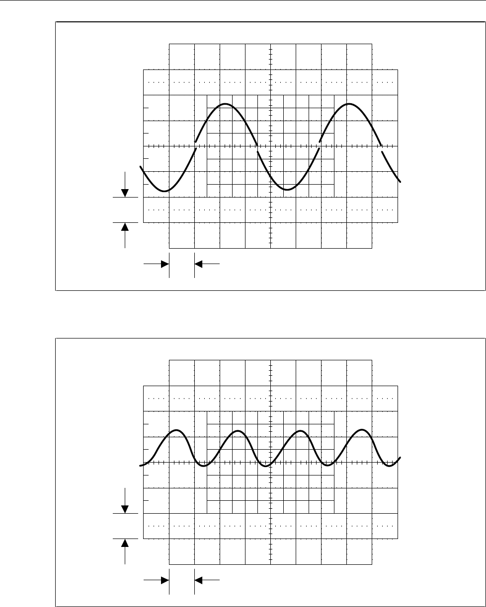
5700A/5720A Series II Calibrator
Service Manual
5-70
1 V
10 ms
F5-27.EPS
Figure 5-27. Waveform at Anode of CR4
1 V
10 ms
F5-28.EPS
Figure 5-28. Waveform at Pin 6 of U11
8. Check the DC SENSE BUFFER and the AC SENSE BUFFER. Set the Calibrator to
1.0V at 1 kHz, operate. Connect an oscilloscope to TP6 (common to TP2) which is
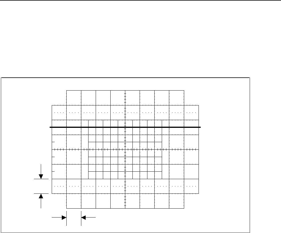
Troubleshooting
Component-level Troubleshooting
5
5-71
the input to the AC/DC sensor. The oscilloscope display should be switching
between Figure 5-29, which is the output of the DC SENSE BUFFER circuit and
Figure 5-30, which is the output of the AC SENSE BUFFER circuit. If either of
these signals is incorrect, check the appropriate SENSE BUFFER circuit as outlined
on the schematic. If these voltages are correct, set the Calibrator to 10.0V at 1 kHz,
operate, and verify the ac amplitude from the AC SENSE BUFFER remains the
same. If a failure is detected, check relay K4 and resistor Z3 in the AC SENSE
BUFFER circuit.
1 V
10 ms
F5-29.EPS
Figure 5-29. DC Sense Buffer Waveform TP6
Note
Before proceeding remove the jumper connecting SDL to SCOM on this
Oscillator Control assembly and the jumper connecting TP9 to TP10 on
the DAC assembly.
9. Check the AC/DC THERMAL SENSOR & SQUARE ROOT AMP. Set the
Calibrator to 1.0V at 1 kHz, operate. Connect a DMM to TP7 (common to TP2)
which is the output of the Fluke RMS Sensor. The DMM should read 3.16V dc ±160
mV. If this voltage is incorrect, check U14, U15, U17, and associated components.
10. Check the RCL ANALOG SWITCHING circuit. Set the Calibrator to 1.0V at 1 kHz,
operate. Connect a DMM to TP8 (common to TP2) which is the RCL line. The
DMM should read the same voltage at TP7 in the previous step. If this voltage is
incorrect, check U19A, K6, and their drive circuitry. Set the Calibrator to 5V at 1
kHz, operate. The DMM connect to TP8 should read 1.58V ±160 mV. If this voltage
is incorrect, check U31, U19B, K7, and their appropriate drive circuit.
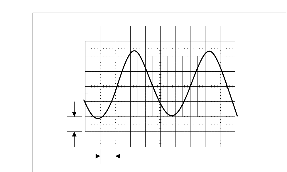
5700A/5720A Series II Calibrator
Service Manual
5-72
1 V
10 ms
F5-30.EPS
Figure 5-30. AC Sense Buffer Waveform at TP6
5-18. Troubleshooting the Oscillator Output Assembly (A13)
Note
During normal Calibrator operation, internal software monitors the output
and makes corrections or trips the instrument to standby. This internal
monitoring can cause problems when attempting to troubleshoot the
Oscillator Output assembly. Defeat the monitoring by connecting a jumper
from TP9 to TP10 on the DAC assembly and another jumper connecting
SDL (P511 pin 11A/11C) to SCOM (TP1) on the Oscillator Output
assembly.
After defeating software monitoring, Remove the front air duct and rear shield from the
Oscillator Output assembly. Place the assembly on the extender card, and proceed as
follows to troubleshoot the Oscillator Output Assembly (A13):
1. Turn on the Calibrator.
2. Check for oscillation at INT OSC OUT. Connect an oscilloscope probe to TP3
(common to TP1). A 100 Hz sine wave at 5.12V rms ±0.25V should be present. If no
oscillation is present proceed with step 3; otherwise skip to step 4.
3. Unsolder and lift up one end of feedback resistor R6. Jumper the input to the
SUMMING AMPLIFIER (the node of R1, R6, and U3 pin 5) to the +5S supply. All
four amplifiers in this oscillator section are inverting amplifiers. With a positive
voltage at the input, check for the following:
• TP5: negative voltage
• TP4: positive voltage
• TP3: negative voltage
• Pin 6 of U8: negative voltage

Troubleshooting
Component-level Troubleshooting
5
5-73
4. Next, jumper the input of the SUMMING AMPLIFIER to the -5S supply and check
the following:
• TP5: positive voltage
• TP4: negative voltage
• TP3: positive voltage
• Pin 6 of U8: positive voltage
5. Repair any amplifier circuits which are not properly inverting. Reinstall feedback
resistor R6. If the 100 Hz oscillation is still not present, check rectifying diodes
CR1-CR4 and the summing resistors in Z6. The output of Z6 is summed with the -
12V reference by R42 and R43. Check the ERROR INTEGRATOR circuit by
making sure opamp U18 is inverting. If it is not, check U18 and its associated
circuitry. If U18 is inverting properly, the problem is probably due to the
MULTIPLIER U16 or its associated components.
6. Check INT OSC OUT for correct oscillation at each frequency range. Connect an
oscilloscope to TP3 (common to TP1). Set the Calibrator for 2V at 100 Hz, 1 kHz,
10 kHz, 100 kHz, and 1 MHz. If any of the frequency ranges are bad (i.e., no
oscillation or oscillation at the wrong frequency range or wrong voltage) check
relays K1, K2, K3, their associated drive circuits, and the amplifier feedback
capacitors that these relays select.
7. Check INT OSC OUT for correct frequency oscillation within a frequency range.
Connect a frequency counter to TP3 (common to TP1). Set the Calibrator for 2V at 5
kHz, operate. Check each frequency digitusing the edit knob. If a failure is detected,
check the FREQ DATA bus D1-D7 (D0 is only used during external phase lock) by
editing the frequency and seeing that each bit toggles between +5V and ground. If
each bit of the FREQ DATA bus is toggling properly the problem is probably due to
resistive DACs U5 and/or U7. If a failure with the FREQ DATA bus is detected,
U32 is probably at fault.
8. Check the 2.2V range output of the Oscillator. Set the Calibrator for 2V at 1 kHz,
operate. Measure the output at TP2 (common to TP1) for an undistorted sine wave of
2V (±50 mV) at 1 kHz with no offset. If the output is incorrect perform the resistor
check as follows:
a. Move switch S1 to the test position (to the left).
b. Measure the voltage drop across R87. It should be 1V ±20%. If this voltage is
incorrect, the 10 mA current source on the Oscillator Wideband SMD (A13A1)
assembly if probably at fault.
c. Verify that the voltage at TP2 is about +3.2V ±0.3V. If this voltage is incorrect,
the output stage circuit is probably at fault. If this voltage is correct the
Oscillator Wideband SMD (A13A1) assembly is probably at fault.
d. Return the switch to the operate position (move to the right).
9. Check the amplitude control within the 2.2V range. Set the Calibrator for 1V at 1
kHz, operate. Edit the amplitude digits and verify the output changes accordingly. If
a problem is detected, edit the output digits again and check each bit (A0-A7) of the
AMPL DATA bus to ensure they toggle between +5V and ground. If they do not,
U12 is probably faulty. If the AMPL DATA bus is operating, the resistive DAC U11
is probably at fault.
10. Check the 22V range output of the Oscillator. Set the Calibrator for 20V at 1 kHz,
operate. Check the output at TP2 (common to TP1) for an undistorted sine wave of
20±0.5V at 1 kHz. If the output is incorrect, check range setting relay K4 and its
associated resistor.

5700A/5720A Series II Calibrator
Service Manual
5-74
11. Check the Phase Lock circuit. Connect a frequency counter to the Calibrator output.
Set the Calibrator to 2V at 1 kHz, operate, and check the frequency accuracy to be
within 0.01% of the nominal. If the frequency is out of tolerance, proceed as follows:
a. Check the ZERO CROSSING DETECTORS by connecting an oscilloscope to
U23 pins 7 and 12 (common = TP1). Ensure they convert the sine wave inputs to
square wave outputs.
b. Check the PHASE DETECTOR outputs by connecting an oscilloscope to U22
pins 5 and 7. With the circuit not phased locked one of these points should be
pulsing. If not, check U22 and associated components.
c. Check the LOOP FILTER & CHARGE PUMP circuit by connecting an
oscilloscope to TP7. With the circuit not phase-locked, TP7 should be either
+13V or -13V. If this voltage is incorrect, check U17, U31A, and associated
components. If this voltage is correct, the problem is probably U19 and/or U15
in the MULTIPLIER circuit.
12. Check the PHASE SHIFTER circuit. Using a dual-channel oscilloscope connect one
channel to the TP2 (oscillator output), and the other channel to TP8 (P SHIFT HI).
Set the Calibrator to 2V at 1 kHz, operate. On the front panel select the "Phase Ctrls
Menu" softkey, followed by the "Phase Shift" softkey to turn the phase shift function
on. The oscilloscope should show two sine waves that are in phase. By pressing the
"Adjust Phase Shift" softkey and then either the softkeys or rotating the edit knob the
phase between these two signal should shift over the entire 360 degree range. If a
failure is detected, first check the control lines for this circuit. On U27 check pin 6
(INHPH) for a logic low, pin 9 (BPH) and pin 10 (APH) should toggle between a
logic high and low depending on the degrees of phase shift selected. If these control
lines are incorrect, check U33. If the control lines are correct check U27, U28, and
the associated components in the PHASE SHIFTER circuit.
5-19. Troubleshooting the High Voltage Control Assembly (A14)
1. Remove the rear shield from the High Voltage Control assembly and place it on the
extender card. All measurements will be referenced to PACOM (TP6) unless Noted
otherwise. Power up the Calibrator and proceed as follows.
Warning
High voltages are exposed when troubleshooting the high
voltage control assembly.
2. Measure the voltage at TP4 with a DMM and verify it is between +0.1 and +0.3V. If
a failure is detected, check U2C, U6, and associated components. Next, power down
the Calibrator and connect an oscilloscope, set for 20V/div and 500 us/div, to TP3.
At power up of the Calibrator the oscilloscope should displays a 1 kHz square wave
which ramps up to the level shown in Figure 5-31, remains there for approximately 1
second, and goes to a 0V. If a failure is detected, skip to the Magnitude Control
circuit troubleshooting in this section.
Note
The following step 3 checks the operation of the High Voltage Control
assembly in the 1100V AC Range. If may be useful to refer to Figure 2-25
in the Theory of Operation Section.
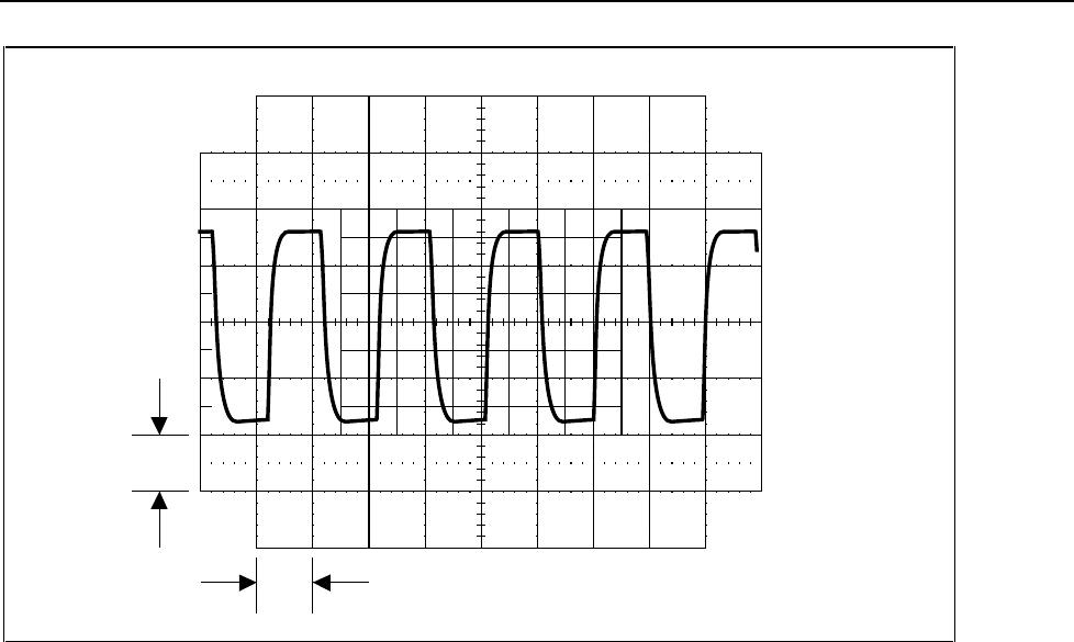
Troubleshooting
Component-level Troubleshooting
5
5-75
1 V
10 ms
F5-31.EPS
Figure 5-31. Waveform at TP3
3. Check the High Voltage Control in the 1100V ac range. Set the Calibrator to 220V at
110 Hz and 130 Hz, operate. At both output frequencies measure with a DMM the ac
voltage at pin 1A or 1C of connector P611 and verify it reads 220±0.2V. In this
range the High Voltage Control assembly and Power Amplifier assembly work
together to form an overall amplifier with a gain of -100. If a failure is detected,
check T1, K1, K14, K15, K16, K9, K6, K5, K12, and K3.
Note
Steps 4 through 7 check the operation of the High Voltage Control
assembly in the 1100V DC Range. If may be useful to refer to Figure 2-26
in the Theory of Operation Section.
4. Check the -SP C and +SP C from the High Voltage/High Current assembly. Set the
Calibrator to 0V standby. Using a DMM, measure the dc voltage at the cathode of
VR4 (-SP C) and verify it is between +13.2 and +14.2V. Next, measure the anode of
VR5 (+SP C) and verify it is-0.1V to -0.3V. If a failure is detected, the HV DC
Output Series Pass & Current Limit Circuit on the High Voltage/High Current
(A15)assembly may be at fault.
5. Check the output from the Magnitude Control circuit. Set the Calibrator to +220V
dc, operate. Connect an oscilloscope to TP3 and verify it displays a signal similar to
the previously shown Figure 5-31, except the amplitude is typically 10V p-p. The
measured amplitude may not be 10V p-p, for now just verify that the 1 kHz signal is
present. If a failure is detected, skip to the Magnitude Control circuit troubleshooting
in this section.
6. Check the High Voltage Control in the 1100V dc Range. Set the Calibrator to +220V
dc, operate. Using a DMM, measure the dc voltage across capacitor C1 and verify it
is 227V ±1V. A problem with the Magnitude Control circuit may cause this voltage
to be much greater than 227V. If no dc voltage is present check T1, K9, K6, CR1-

5700A/5720A Series II Calibrator
Service Manual
5-76
CR4, and associated components. If the measure voltage is much greater than 227V
skip to the Magnitude Control Circuit troubleshooting starting at step 10.
7. Check HV OUT from the High Voltage Control assembly. Set the Calibrator to
+220V dc, operate. Using a DMM measure the dc voltage at pin 1A or 1C of P611
and verify it reads +220V ±0.2V. If a failure is detected, check K4, K11, K5, K12,
K3, and associated components.
Note
The following steps 8 and 9 check the operation of the High Voltage
Control assembly in the 2.2A Current Range. For these checks it will be
necessary to install a jumper connecting the front panel OUTPUT HI
binding post to the OUTPUT LO binding post. If may be useful to refer to
Figure 2-27 in the Theory of Operation Section.
8. Check the output from the Magnitude control circuit. Set the Calibrator to 220 mA
dc at 1 kHz, operate. Connect an oscilloscope to TP3 and verify it displays a signal
similar the previously shown Figure 5-31, except the amplitude is typically 40V p-p.
The measured amplitude may not be 40V p-p, for now just verify that the 1 kHz
signal is present. If a failure is detected, skip to the Magnitude Control circuit
troubleshooting in this section.
9. Check the High Voltage Control assembly in the 2.2A Range. Set the Calibrator to
220 mA at 1 kHz, operate. Connect the DMM low to VICOM (pins 16A/C of P612)
and the DMM high to VI+ (pins 15A/C of P612)and verify it is +5.3V ±10%. Next,
move the DMM high to VI- (pins 14A/C of P612) and verify it is -5.3 ±10%. If a
failure is detected, check T1, K14, K2, CR5, and associated components in the 2A
Range Power Supply Filter circuit.
Note
Remove the front panel jumper connecting OUTPUT HI to OUTPUT LO
before continuing.
5-20. Magnitude Control Circuit
Proceed as follows to troubleshoot the magnitude control circuit:
1. Check the Square Wave Generator. Power down the Calibrator and connect the
oscilloscope, set for 2V/div and 500 us/div, to TP2. When the Calibrator is turned
on, the oscilloscope should display a TTL-level 1 kHz square wave for
approximately 1 second. If a failure is detected, check U4, U7A, and associated
components in the Square Wave Generator.
2. Check the Reference and Error Amplifier. Power down the Calibrator and connect an
oscilloscope, set for 5V/div, to the cathode of CR10. At power up of the Calibrator
the oscilloscope should display a dc voltage which ramps up to approximately +14V
and remains there for approximately 1 second before returning to 0V. If a failure is
detected, check U2D, U7B, Q2, Q4, VR1, and associated components in the
Reference and Error Amplifier circuit.
3. Check the Square Wave Amplifier. Power down the Calibrator and connect an
oscilloscope, set for 5V/div, to pin 1 of U1. At power up of the Calibrator the
oscilloscope should display a dc voltage which ramps down to approximately -14V
and remains there for approximately 1 second before returning to 0V. If a failure is
detected, check U1A and associated components. If this voltage is correct and at

Troubleshooting
Component-level Troubleshooting
5
5-77
power up there is still no signal at TP3 during power up then check U3, U7C/D, and
associated components in the Square Wave Amplifier circuit.
4. Check the Absolute Value Circuit. Add a jumper connecting the front panel
OUTPUT HI binding post to the OUTPUT LO binding post. Set the Calibrator to
1.0A at 1 kHz, operate. Connect an oscilloscope to G OUT(pin 12C of P612) and
Note the amplitude of the positive wave peaks. Next, connect the oscilloscope to U2
pin 7 and verify the dc voltage is equal the previously Noted positive peaks of ac
voltage. If a failure is detected, check U2A, U2B, and associated components in the
Absolute Value Circuit.
Note
Remove the front panel jumper connecting OUTPUT HI to OUTPUT LO
before continuing.
5. Check the Signal/Polarity Selection. Set the Calibrator to 220V dc operate. Using a
DMM measure the dc voltage at TP4 and verify it is +6 to +8V. Next, set the
Calibrator to -220V dc operate and again verify that the dc voltage at TP4 remains
between +6 and +8V. If a failure is detected, check U2C, U6, and associated
components in the Signal/Polarity Selection circuit.
5-21. Troubleshooting the High Voltage/High Current Assembly (A15)
Proceed as follows to troubleshoot the High Voltage/High Current Assembly (A15):
1. Remove the rear shield from the High Voltage/High Current assembly and place it
on the extender card. All measurements will be referenced to ACOM (TP7) unless
Noted otherwise. Power up the Calibrator and proceed as follows.
Warning
High voltages are exposed when troubleshooting the high
voltage/high current assembly.
2. Check the ±20S supplies. Set the Calibrator to 0V dc, standby. Measure with a
DMM the dc voltage at the cathode of VR3 and verify it is 20V±5%. Next, measure
the dc voltage at the anode of VR4 and verify it is -20V ±5%. If a failure is detected,
check VR3, VR4, and associated components.
3. Check the power-up standby voltages. Set the Calibrator to 0V standby. Using a
DMM measure the dc voltage at TP5 and verify it is 0V ±50 µV. If a failure is
detected, proceed with step 4, otherwise skip to step 6.
4. Check Buffer U1. Measure the dc voltage at TP3 and Note the polarity. Next,
measure the dc voltage at TP5 and verify that it is the opposite polarity. If a failure is
detected, check U1 and associated components.
5. Check the HR7 Hybrid and U2. Measure the dc voltage at pin 10 of the HR7 Hybrid
and Note the polarity. Next, measure the dc voltage at TP3 and check that it is the
opposite polarity. If a failure is detected, check the HR7 Hybrid, U2, and associated
components.
6. Check -SP C and +SP C at power up standby. Using a DMM, measure the dc voltage
at TP4 (-SP C) and verify it is between +13.2 and +14.2V. Next measure the dc
voltage at TP6 (+SP C) and verify it is between-0.1 and -0.3V. If a failure is
detected, check Q3, Q4, Q6, and associated components in the HV DC Output Series
Pass & Current Limit circuit.
7. The following step 8 checks the High Voltage/High Current assembly in the 1100V
ac range. To better understand of function of this assembly during this mode of

5700A/5720A Series II Calibrator
Service Manual
5-78
operation refer to Figure 2-25 in the Theory of Operation section. During normal
operation in the 1100V ac mode, internal software monitors the output and makes
corrections or trips the instrument into standby. This internal monitoring can cause
difficulty when troubleshooting a faulty High Voltage assembly. If during the next
step 8 the instrument keeps tripping into standby, defeat the monitoring by
connecting a jumper from TP9 to TP10 on the DAC assembly.
8. Check the 1100V ac range. Set the Calibrator to 220V at 130 Hz, operate. Using a
DMM, measure the ac voltage at pin 1 of the HR7 resistor network. Note the DMM
reading and verify it is 220V ac ±0.1V. Next, measure the voltage at TP5 and verify
it is 1/100th of the voltage Noted at pin 1 of the HR7 resistor network. If a failure is
detected, check the HR7 Hybrid assembly, U2, U1, K6, K1, K4, and associated
components.
Note
Remove the jumper connecting TP9 to TP10 on the DAC assembly before
continuing. Steps 10 through 12 check the High Voltage/High Current
assembly in the 1100V dc range. To better understand the function of this
assembly during this mode of operation, refer to Figure 2-26 in the Theory
of Operation section.
9. Check the 1100VDC Range input voltage. Set the Calibrator to 220V dc, operate.
Using a DMM measure the dc voltage at TP1 and verify it is-2.2V ±1 mV. If a
failure is detected, check K1 and its drive circuit.
10. Check the 1100VDC Range DC HV Amplifier. Set the Calibrator to 220V dc,
operate. Measure the dc voltage at TP3 with a DMM and verify it is 0.55±0.2V.
Next, set the Calibrator to -220V dc, operate. Again measure the dc voltage at TP3
and verify it is now 2.3±0.2V. If a failure is detected, check the HR7 Hybrid
assembly, U2, K5, K7, K14, and associated components.
11. Check -SP C and +SP C in the 1100V dc range. Set the Calibrator to +220 Vdc,
operate. Using a DMM, measure the dc voltage at TP4 (-SP C) and verify it is
between +13.2 and +14.2V. Also measure the dc voltage at TP6 (+SP C) and verify
it is between -6 and -8V. Next, set the Calibrator to -220V dc, operate. Again
measure the dc voltage at TP4 and TP6. In this mode TP4 should be between +6 and
+8V, and TP6 should be between -13.2 and -14.2V. If a failure is detected, check
Q3, Q4, Q6, and associated components.
Note
Steps 12 through 14 check the High Voltage/High Current assembly in the
2.2A Current range. For these checks it will be necessary to install a
jumper connecting the front panel OUTPUT HI binding post to the
OUTPUT LO binding post. To better understand the function of this
assembly during this mode of operation refer to Figure 2-27 in the Theory
of Operation section.
12. Remove the hybrid cover from the H4 assembly. Unsolder the right end of resistor
R37 (node with R37, Z5 pins 2 and 3), labeled G+ on the schematic, and lift this end
out of the circuit board. Connect an external ac reference to the lifted end of R37 and
reinstall the assembly on the extender card. Power up the Calibrator. Set the external
ac reference to 1V at 1 kHz and connect an oscilloscope to the output of the H4
Hybrid (node with R42, R44, and H4 pin 18). Verify the oscilloscope displays a
square wave similar to Figure 5-32. If a failure is detected, check the H4 Hybrid
assembly.
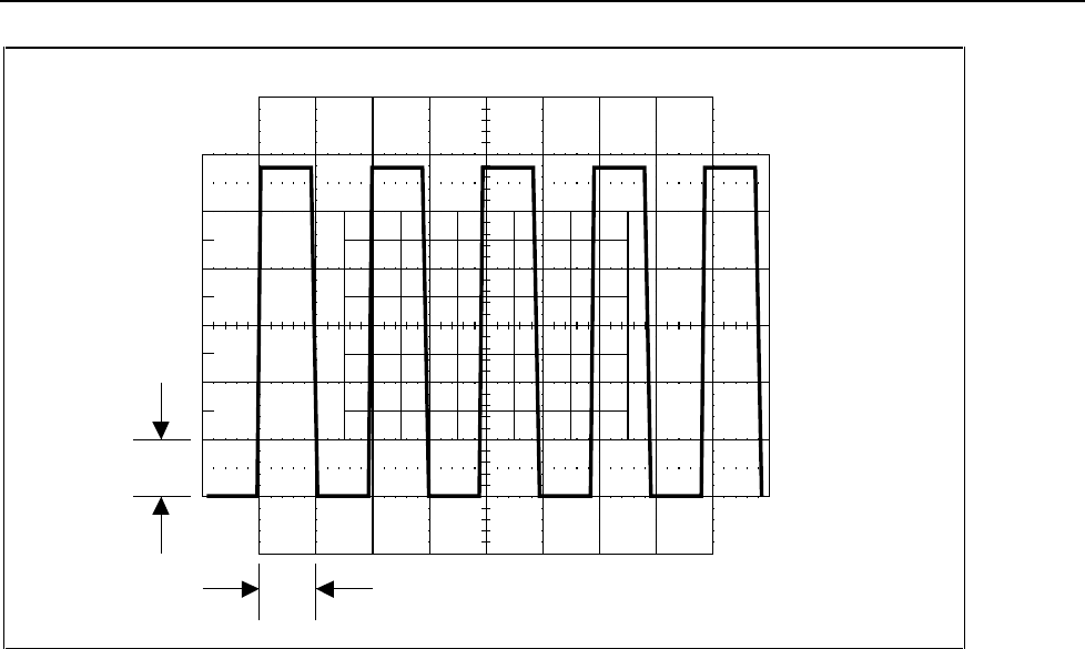
Troubleshooting
Component-level Troubleshooting
5
5-79
1 V
10 ms
F5-32.EPS
Figure 5-32. Waveform at Pin 18 of Hybrid H4
13. Connect an oscilloscope to pin 7 of U3B and verify it displays a square wave equal
to the positive peaks of Figure 5-32. Next, connect the oscilloscope to pin 1 of U3A
and verify it displays a square wave equal to the negative peaks of Figure 5-32. If a
failure is detected, check U3 and associated components.
Note
Reinstall the lifted end of R37, solder it to the circuit board, and reinstall
the H4 Hybrid cover before continuing.
14. Check the 2.2A current range. Set the Calibrator to 0A in the 2.2A Range by range
locking the instrument in the 2.2A range and calling up 0A. Using a DMM, measure
the dc voltage across R57 and verify it is 0.028V ±25%. Next, measure the dc
voltage across R68 and verify it is 0.028V ±25%. If a failure is detected, check U4,
U5, Q11-Q16, and associated components.
5-22. Troubleshooting the Power Amplifier Assembly (A16)
Note
During normal Calibrator operation, internal software monitors the output
and makes corrections or trips the instrument to standby. This internal
monitoring can cause problems when attempting to troubleshoot the Power
Amplifier assembly. Defeat the monitoring by connecting a jumper from
TP9 to TP10 on the DAC assembly and another jumper connecting TP1 on
the Oscillator Output (A13) assembly to the bottom of R8 (node with R8,
C42, C43, and pin 6 of U6) on the Oscillator Control (A12) assembly.
After disabling the internal moitoring loop, remove the rear shield and front air duct
from the Power Amplifier assembly. Place the assembly on the extender card and
proceed as follows to troubleshoot the Power Amplifier assembly (A16):
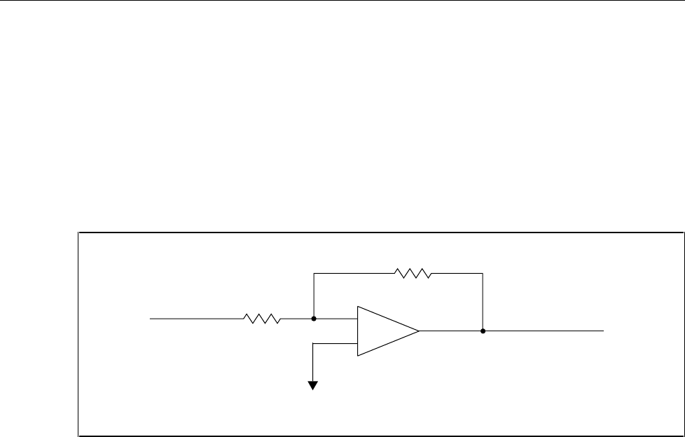
5700A/5720A Series II Calibrator
Service Manual
5-80
1. Power up the Calibrator. In the following steps, reference all measurements to
PACOM (TP10) unless otherwise Noted.
2. Set the Calibrator to 22V at 1 kHz, operate. This configures the Power Amplifier
assembly as an amplifier with a gain of -10 as shown in Figure 5-33. Check the input
for the correct voltage. Using a DMM, measure the ac voltage at TP3 and verify it is
2.2V ±5%. If this voltage is incorrect, check relay K10A and its drive circuit. Next,
measure the output of the Power Amplifier. Using a DMM, measure the voltage at
TP6 and verify it is 10 times that measured at TP3 ±5%. Also measure the dc offset
at TP6 and verify it is less than 10 mV. If this voltage is incorrect, proceed with step
3. If the output voltage is correct skip to step 8.
50K
PA OUT HI
OSC OUT HI
PACOM
22-220V
2.2 -22V
50K
-
+
F5-33.EPS
Figure 5-33. Power Amplifier with Calibrator Set to 22V at 1 kHz
3. Before troubleshooting the main Power Amplifier loop, switch the ±PA supplies to
the low voltage (±40SR Supplies) mode by switching switch SW201 on the
Filter/PA Supply assembly. Using a DMM, measure the ±PA supplies and verify
they are ±60V ±15V. If a failure is detected, the Filter/ PA Supply assembly may be
at fault.
4. Check the Bias Current circuit. Set the Calibrator to 0V dc, standby. Connect an
external 100Ω 1/4W carbon-film resistor between PACOM (TP10) and 1ST MID
STAGE OUT which is the left side of 1W resistor R41. Using a DMM, measure the
mid stage output (1ST MID STAGE OUT),which is the left side of R41, and verify
the dc voltage is either +0.8V ±0.2V or -1.1V ±0.2V. If this voltage is correct skip to
step 6. If it is incorrect, remove Q12 from the assembly and recheck the Mid-Stage
output. With Q12 removed, the Mid-Stage output should be 0.8V ±0.2V. If this
voltage is incorrect, check CR53, Q31, Q32, and associated components in the
Current Source Circuit. If the voltage is correct then the Input Stage or Mid-Stage
circuitry is probably at fault.
5. Check the Input Stage and Mid-Stage. Set the Calibrator to 0V dc, standby. Using a
DMM check measure the voltage at pin 10 of the HR8 hybrid and Note whether it is
positive or negative. Next, measure the Input Stage output at TP4 and verify it is
properly inverting. If a failure is detected, the Input Stage circuit is probably at fault.
If the Input Stage is properly inverting, the Mid-Stage circuit is probably at fault.
6. Check the Output Stage Bias Current. Set the Calibrator to 0V dc, standby. Connect
an external 100Ω 1/4W carbon-film resistor between PACOM (TP10) and 1ST MID
STAGE OUT which is the left side of 1W resistor R41. Using a DMM measure the
Output Stage bias current by measuring the dc voltage between TP14 and TP15,
verify it is 0.92V±20%. If a failure is detected, check Q7, Q4, Q5, Q10, Q11, and
associated components.

Troubleshooting
Component-level Troubleshooting
5
5-81
7. Check the output of the Output Stage. Set the Calibrator to 0V dc, standby. Connect
an external 100Ω 1/4W carbon-film resistor between PACOM (TP10) and 1ST MID
STAGE OUT, which is the left side of 1W resistor R41. Measure the dc voltage at
the Mid-Stage output as is step 4. If the voltage is +0.8V, then the voltage at TP6
(PA OUT HI)should be +3.2±0.3V. If the voltage measured at the Mid-Stage output
is -1.1V, then the voltage at TP6 should be +1.3±0.3V. If a failure is detected, check
the components in the Output Stage Circuit.
Note
If switch SW201 on the Filter/PA Supply assembly was set to the low
voltage mode, switch it back to the normal(±PA) mode before continuing.
8. Check the 220V RANGE AC ATTENUATOR. Connect a jumper from TP9 to TP10
on the DAC assembly and another jumper connecting TP1 on the Oscillator Output
(A13) assembly to the bottom of R8 (node with R8, C42, C43, and pin 6 of U6) on
the Oscillator Control (A12) assembly as done in the previous step 1. Set the
Calibrator to 22V at 1 kHz, operate. Testing of this 220V Range AC Attenuator is
divided into three steps. Measure the ac voltage with a DMM at TP6 (the Power
Amplifier output), then measure the voltage at TP7 (Attenuator input) and verify
they are the same ±10 mV. If a failure is detected, check relay K16B and its drive
circuit.
Note
If relay K16B is not at fault, then PA OUT HI may be open from PA SENSE
AC elsewhere in the Calibrator.
9. Measure the ac voltage at TP8 with a DMM and verify it equals the voltage
measured at TP7 divided by 100 ±1%. Also use an oscilloscope and check for any
distortion at TP8. If a failure is detected, check Z1, U4, Q58, Q54, and their
associated components. Next, using a DMM, measure the ac voltage at pin 8 of K11
and verify it is the same as measured at TP8. If a failure is detected, check relays
K10B, K11, and their drive circuit.
10. Check the SC+ and SC- supplies. Set the Calibrator to 0V dc, standby. Using a
DMM, measure the SC+ supply at U1 pin 7 and verify it is +18V ±10%. Next,
measure the DC- supply at U1 pin 4 and verify it is -15V ±10%. If a failure is
detected, check zener diodes VR15 and VR18.
Note
Remove any jumpers left in place from step 8 before continuing.
11. Check the SENSE CURRENT CANCELLATION circuit. Set the Calibrator to 100
Vdc, operate. Using a DMM, measure the voltage between pin 6 of U1 and TP1, and
verify it is 2V ±25 mV. If a failure is detected, check U1 and its associated
components.
Note
Step 12 should be done only when a problem with calibration of the 220V
dc range exists.
12. Check the 220V DC INT. CAL. NETWORK. Set the Calibrator to 0V dc, standby.
Connect a jumper from U5 pin 1 to SCOM (TP11). Using a DMM measure the 13V
reference at TP2 of the DAC assembly (common to TP3)and Note the reading. Next,
measure the buffered 13V reference at TP12 of the Power Amplifier and verify it is
the same. If a failure is detected, check U5, K3, and their drive circuit. Next, using a

5700A/5720A Series II Calibrator
Service Manual
5-82
DMM, measure the voltage at U9 pin 6 and verify it is the equal to the voltage at
TP12 divided by 8 ±1%. If a failure is detected, check the HR8 resistor network, U9,
and the associated components.
5-23. Troubleshooting the Filter/PA Supply Assembly (A18)
Proceed as follows to troubleshoot the Filter/PA Supply assembly (A18):
1. Place the Filter/PA Supply assembly on the extender card. Remove the Power
Amplifier assembly (A16) and power up the Calibrator. Reference all measurements
to PACOM (TP203). The Calibrator should be in its power-up default standby
condition unless otherwise Noted.
2. Check the unregulated ±250V Supplies. Using a DMM, measure the dc voltage at
the cathode of CR235 or CR239 and verify it is -280V±10%. Next, measure the dc
voltage at the anode of CR208 or CR203 and verify it is +280V ±10%. Connect an
oscilloscope to these points and verify the ripple is less than 5V p-p. If a failure is
detected, check CR222, F202, F203, and associated components.
3. Check the unregulated ±500V Supplies. Using a DMM measure the dc voltage at
TP209 and verify it is +565 ±10%. Next, measure the dc voltage at TP211 and verify
it is -565 ±10%. Connect an oscilloscope to these points and verify the ripple is less
than 5V p-p. If a failure is detected, check CR217, CR218, CR220, CR221, CR223,
CR224, CR227, CR228, F201, F204, and associated components.
4. Check the Control Lines. Using a DMM, measure the dc voltage at TP205, TP207,
and TP208. Verify they are all at +12V ±4V. Next measure the dc voltage at pins 13
and 14 of U201. Verify they are at- 12V ±4V. If a failure is detected, check Z201,
U201A, U201B, and associated components.
5. Check the unregulated +250V Supply. Using a DMM, measure the dc voltage at
TP210 and verify it is +280 ±10% If a failure is detected, measure the voltage at the
cathode of VR211 and verify it is +140 ±20%. If this voltage is incorrect, check
VR211, VR214, VR215, VR219, and Q208. If the voltage at the cathode of VR211
is correct then check Q201, CR201, CR203, CR208, CR210, and associated
components.
6. Check the regulated +PA Supply at 0V. Using a DMM measure the dc voltage at
TP201 and verify it is less than 1.0V. If a failure is detected, check Q207.
7. Check the regulated +PA Supply at +180V. Jumper TP207 to PACOM (TP203),
measure the +PA Supply at TP201 and verify it is +190V±10%. If this voltage is
correct, skip to step 8, otherwise continue as follows. Measure the output of the
Current Limit circuit. Connect a DMM to pin 1 of U201 and verify it is -12±4V. If
this voltage is incorrect, then the +PA Supply is current-limited. Check the output
for shorts and check the current-limiting circuit contained in U201C, Q203, Q206,
and associated components. If the voltage at pin 1 of U201 is correct, check Q205,
Q202, VR212, VR207, and associated components.
8. Check the unregulated +PA Supply at +360V. Jumper TP207 and TP205 to PACOM
(TP203), measure the voltage at TP210 and verify it is +480V±10%. If a failure is
detected, check Q208, VR214, VR215, VR219, CR201, CR203, CR208, CR210, and
associated components. Next, check the regulated +PA Supply at TP201 and verify it
is +370V ±10%. If a failure is detected, check Q205 and VR216.
9. Check the Current Limiting of the +PA Supply. Jumper TP207 to PACOM (TP203)
and remove the jumper connecting TP205 to LO HI I (TP206). Connect an
oscilloscope to the +PA Supply at TP201. Connect a 1 kΩ 10W resistor (such as
Fluke P/N 157933) between PACOM (TP203) and the +PA supply output at Jumper

Troubleshooting
Component-level Troubleshooting
5
5-83
J201. The +PA supply (at +180V)should go into current limit. The oscilloscope
should show a repeating pattern in which the +PA supply climbs to about +180V
then drops to 0V. If a failure is detected, check Q203, VR246, VR213, U201C, and
associated components.
10. Check the unregulated -250V Supply. Using a DMM, measure the dc voltage at
TP212 and verify it is -280V ±10%. If a failure is detected, measure the voltage at
the anode of VR231 and verify it is-140V ±20%. If this voltage is incorrect, check
VR231, VR230, VR229, VR225, and Q209. If the voltage at the anode of VR231 is
correct, then check Q215, CR234, CR235, CR239, CR243, and associated
components.
11. Check the regulated -PA Supply at 0V. Using a DMM, measure the dc voltage at
TP204 and verify it is less than 1.0V. If a failure is detected, check Q212.
12. Check the regulated -PA Supply at -180V. Jumper TP207 to PACOM (TP203),
measure the -PA Supply at TP204 and verify it is -190V±10%. If this voltage is
correct, skip to step 13, otherwise continue as follows. Measure the output of the
Current Limit circuit. Connect a DMM to pin 2 of U201 and verify it is +12±4V. If
this voltage is incorrect, then the -PA Supply is in current limit. Check the output for
shorts and check the current-limiting circuit contained in U201D, Q211, Q214, and
associated components. If the voltage at pin 2 of U201 is correct check Q210, Q216,
VR232, VR238, and associated components.
13. Check the unregulated -PA Supply at -360V. Jumper TP207 and TP208 to PACOM
(TP203), measure the voltage at TP212 and verify it is-480V ±10%. If a failure is
detected, check Q209, VR225, VR229, VR230, CR234, CR235, CR239, CR243, and
associated components. Next, check the regulated -PA Supply at TP204 and verify it
is -370V±10%. If a failure is detected, check Q210, and VR226.
14. Check the Current Limiting of the -PA Supply. Jumper TP207 to PACOM (TP203)
and remove the jumper connecting TP208 to LO HI I (TP206). Connect an
oscilloscope to the -PA Supply at TP204. Connect a 1 kΩ 10W resistor (such as
Fluke P/N 157933) between PACOM (TP203) and the -PA supply output at Jumper
J202. The -PA supply (at -180V)should go into current limit. The oscilloscope
should show a repeating pattern in which the -PA supply climbs to about -180V then
drops to 0V. If a failure is detected, check Q214, VR247, VR233, U201D, and
associated components.

5700A/5720A Series II Calibrator
Service Manual
5-84
6-1
Chapter 6
List of Replaceable Parts
Title Page
6-1. Introduction..........................................................................................6-3
6-2. How to Obtain Parts.............................................................................6-3
6-3. Manual Status Information...................................................................6-3
6-4. Newer Instruments................................................................................6-3
6-5. Service Centers.....................................................................................6-4

5700A/5720A Series II Calibrator
Service Manual
6-2

List of Replaceable Parts
Introduction
6
6-3
6-1. Introduction
This section contains an illustrated list of replaceable parts for the 5700A/5720A Series
II. Where applicable, parts differences are indicated between the 5700A and 5720A. For
example, Table 6-1 indicates MP36 (nameplate) is PN 600723 for a 5700A or PN
600759 for a 5720A. Parts are listed by assembly; alphabetized by reference designator.
Each assembly is accompanied by an illustration showing the location of each part and
its reference designator. The parts lists give the following information:
• Reference designator
• An indication if the part is subject to damage by static discharge
• Description
• Fluke stock number
• Manufacturers supply code
• Manufacturers part number or generic type
• Total quantity
• Any special notes (i.e., factory-selected part)
CAUTION
A * symbol indicates a device that may be damaged by static
discharge.
6-2. How to Obtain Parts
Electrical components may be ordered directly from the manufacturer by using the
manufacturer’s part number, or from Fluke Corporation and its authorized
representatives by using the part number under the heading FLUKE STOCK NO. Parts
price information is available from the Fluke Corporation or its representatives. Prices
are also available in a Fluke Replacement Parts Catalog which is available on request.
In the event that the part ordered has been replaced by a new or improved part, the
replacement will be accompanied by an explanatory note and installation instructions, if
necessary.
To ensure prompt delivery of the correct part, include the following information when
you place an order:
• Instrument model and serial number
• Part number and revision level of the pca containing the part
• Reference designator
• Fluke stock number
• Description (as given under the DESCRIPTION heading)
• Quantity
Refer to Contacting Fluke earlier in this manual for more information.
6-3. Manual Status Information
The Manual Status Information table that precedes the parts list defines the assembly
revision levels that are documented in the manual. Revision levels are printed on the
component side of each pca.
6-4. Newer Instruments
Changes and improvements made to the instrument are identified by incrementing the
revision letter marked on the affected pca. These changes are documented on a
supplemental change/errata sheet which, when applicable, is included with the manual.

5700A/5720A Series II Calibrator
Service Manual
6-4
6-5. Service Centers
To locate a service center, use the information located in Contacting Fluke earlier in this
manual.
Manual Status Information
Ref or
Option
No.
Assembly Name Fluke
Part No.
Revision
Level
A1 Keyboard PCA 761049 D
A2 Front Panel PCA 761031 102
A3 Analog Motherboard PCA 761023 100
A4 Digital Motherboard PCA 760942 101
A5 WideBand Output PCA 761346 105
A6 Wideband Oscillator PCA 761098 104
A7 Current/High-Resolution Oseillator PCA 764613 203
A8 Switch Matrix PCA 761106 105
A9 Ohms Cal PCA 775395 100
A10 Ohms Main PCA 761114 100
A11 DAC PCA 761122 104
A11A1 DAC Filter PCA 761395 B
A11A2 DAC Buffered Reference PCA 764639 A
A12 Oscillator Control PCA 761130 105
A13 Oscillator Output PCA 1607704 003
A13A1 Oscillator Wideband PCA 761403 C
A14 High Voltage Control PCA 775429 100
A15 High Voltage/High Current PCA 761155 100
A16 Power Amplifier PCA 761163 105
A16A1 Power Amplifier Digital Control SIP PCA 775320 C
A17 Regulator/Guard Crossing PCA 761171 105
A18 Filter/PA Supply PCA 761189 106
A19 Digital Power Supply PCA 761056 104
A20 CPU PCA (5700A Series I) 1591070 108
A20 CPU PCA (5700A Series II) 1639013 107
A20 CPU PCA (5720A) 1626228 108
A21 Rear Panel PCA 761221 101
A92 Oscillator Amp 761403 101
A93 DAC Filter 761395 B1
A95 Buffered Reference 764639 A1

List of Replaceable Parts
Service Centers
6
6-5
Table
6-
1. Front Panel Final Assembly
Reference
Designator Description Fluke Stock
No Tot Qty Notes
A1 * KEYBOARD PCA 761049 1
A2 * FRONT PANEL PCA 761031 1
A3 * ANALOG MOTHERBOARD PCA 761023 1
A4 * DIGITAL MOTHERBOARD PCA 760942 1
A7 * CURRENT/HIGHT RESOLUTION OSCILLTOR. PCA 764613 1
A8 * SWITCH MATRIX PCA 761106 1
A9 * OHMS,CAL PCA 775395 1
A10 * OHMS,MAIN PCA 761114 1
A11 * DAC PCA 761122 1
A12 * OSCILLATOR CONTROL PCA 761130 1
A13 * OSCILLATOR OUTPUT, PCA 761148 1
A14 * HIGH VOLTAGE CONTROL PCA 775429 1
A15 * HIGH VOLTAGE/HIGH CURRENT PCA 761155 1
A16 * POWER AMPLIFIER PCA 761163 1
A17 * REGULATOR./GUARD CROSSING PCA 761171 1
A18 * FILTER/PA PCA 761189 1
A19 * DIGITAL POWER SUPPLY PCA 761056 1
A20 * CPU PCA (5700 Series I) 1591070 1
A20 * CPU PCA (5700 Series II) 1639013 1
A20 * CPU PCA (5720A) 1626228 1
A21 * REAR PANEL PCA 761221 1
A22 TRANSFORMER/MODULE ASSEMBLY 813527 1 1
CP1 ADAPTER,COAX,SMA(F),N(F) 516963 1
E1 JUMPER LINK,BINDING POST 190728 1
E2 GROUND STRIP,COPPER,1.00,.375,.030 854836 1
H5 SCREW,PH,P,THD FORM,STL,5-20,..312 494641 9
H20 SCREW,PH,P,LOCK,STL,4-40,.187 129882 4
H25 SCREW,CAP,SCKT,SS,8-32,.375 837575 4
H29 SCREW,FHU,P,LOCK,SS,6-32,.250 769893 3
H32 SCREW,PH,P,LOCK,STL,6-32,.250 152140 11
H43 SCREW,PH,P,LOCK,SS,6-32,.375 334458 1
MP1 PANEL, FRONT, SHEET METAL 761437 1
MP2 SHIELD, DISPLAY PWB 764514 1
MP3 LENS, SHIELD 760843 1
MP4 DECAL, FRONT OUTPUT CABLE DIAGRAM 802967 1
MP6 GROMMET,EXTRUDED,POLYETHYLENE,.085 854351 1
MP14 BINDING POST-RED 886382 3
MP17 BINDING POST-BLACK 886379 2
MP19 BINDING POST-GREEN 886374 1
MP20 BINDING POST-BLUE 886366 1
MP21 ENCODER WHEEL 764548 1
MP22 FRONT PANEL, MOLDED 886325 1
MP23 KNOB, ENCODER, GREY 868794 1
MP24 KEYPAD,ELASTOMERIC 1586631 1
MP25 DECAL, POWER ON/OFF 886312 1
MP26 DECAL, KEYPAD 886304 1
MP27 DECAL, FRONT OUTPUT 886309 1
MP28 NUT, #8 LOW THERMAL 850334 8
MP35 LENS, DISPLAY 600756 1
MP36 NAMEPLATE SET, ELECTROFORM (MODEL 5700A) 600723 1
MP36 NAMEPLATE SET, ELECTROFORM (MODEL 5720A) 600759 1
MP37 HANDLE,INSTRUMENT 886333 2
TM1 5700A/5720 OPERATOR MANUAL 601622 1
TM2 5700A/5720A SERVICE MANUAL 601630 1
TM3 5700A/5720A SERIES GUIDE SET 601960 1
1. See Figure 6-1a.
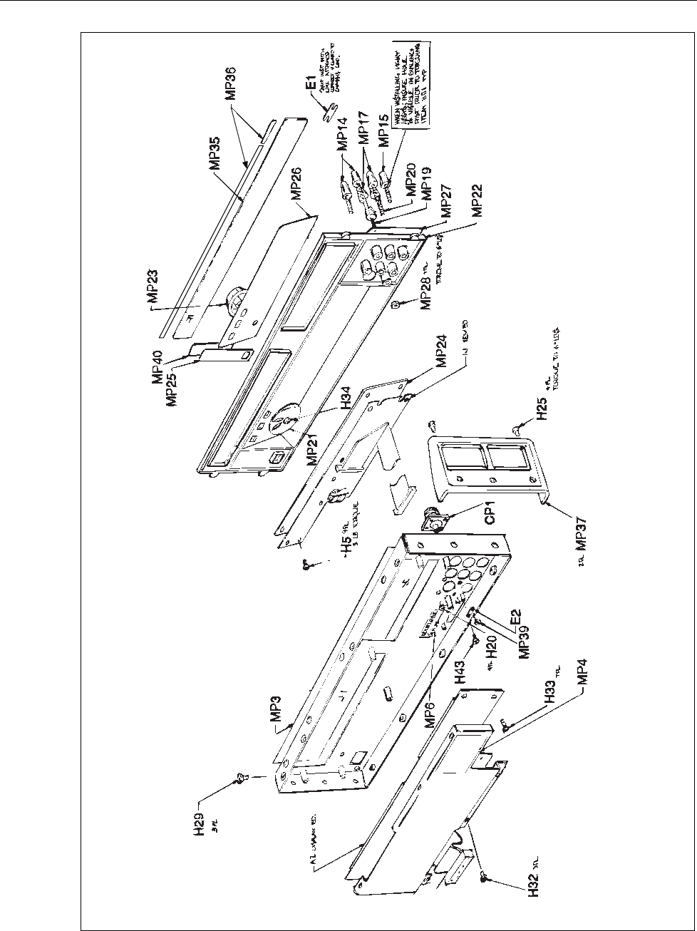
5700A/5720A Series II Calibrator
Service Manual
6-6
5700A-T&B
f6-1.eps
Figure 6-1. Front Panel Final Assembly
List of Replaceable Parts
Service Centers
6
6-7
Table 6-1. Chassis Final Assembly
Reference
Designator Description Fluke Stock
No Tot Qty Notes
A22 TRANSFORMER/MODULE ASSEMBLY 813527 1 1
B1,B2 FAN/CONNECTOR ASSEMBLY 761213 2
E1 BINDING HEAD, PLATED 102889 1
F1 FUSE,.25X1.25,1.25A,250V,SLOW 109231 1
H1 INSULATOR, ANALOG BOTTOM 775361 1
H2 SCREW,PH,P,LOCK,SS,6-32,.500 320051 9
H14 SCREW,PH,P,LOCK,STL,6-32,.750 114223 14
H21 SCREW,PH,P,LOCK,STL,6-32,.250 152140 27
H43 SCREW,PH,P,LOCK,STL,6-32,.375 152165 2
H45 SCREW,CAP,SCKT,SS,8-32,.375 295105 12
H57 SCREW,FHU,P,LOCK,SS,6-32,.250 769893 17
H74 SCREW,PH,P,LOCK,STL,6-32,1.250 159756 8
H85 WASHER,FLAT,STL,.149,.375,.031 110270 4
H97 WASHER,FLAT,STL,.160,.281,.010 111005 10
H105 SCREW,TH,P,LOCK,STL,8-32,.250 853622 4
MP1 COVER, DIGITAL 775635 1
MP2 BOTTOM COVER, ANALOG BOX 874912 1
MP3 TOP COVER, ANALOG BOX 764522 1
MP4 RELAY BRACKET 761015 1
MP5 TOP COVER, INSTRUMENT 660941 1
MP6 BOTTOM COVER, INSTRUMENT 660944 1
MP7 SHROUD, CPU CABLE 813519 1
MP8 NUT, #8 LOW THERMAL 850334 8
MP11 POWER BUTTON, ON/OFF 775338 1
MP12 BOTTOM FOOT, MOLDED, GRAY #7 868786 4
MP18 SIDE EXTRUSION 886288 2
MP20 ADHESIVE SIDE TRIM 698316 2
MP22 DECAL, CAUTION 240V 760926 2
MP23 DECAL, CAUTION 900V 760934 1
MP31 WASHER, LOW THERMAL #8 859939 16
MP45 INSERT EXTRUSION 886283 2
MP47 INSULATOR, DIGITAL MOTHERBOARD 761247 1
MP54 AIDE,PCB PULL 541730 2
MP108 FOOT,RUBBER,ADHES,GRY,.44 DIA,.20 THK 1601870 3
MP114 GROMMET,SLOT,RUBBER,.438,.062 853291 1
W1 CABLE, WIDEBAND TO FRONT PANEL 802785 1
1. Non-repairable part.
Fuse part number 109231 in all units.
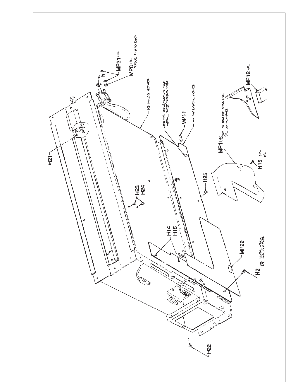
5700A/5720A Series II Calibrator
Service Manual
6-8
5700A T&B
(1 of 2)
f61a1.eps
Figure 6-2. Chassis Final Assembly
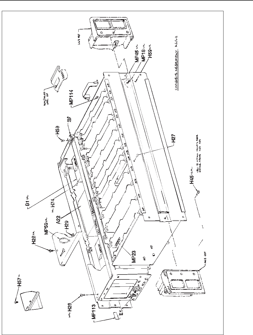
List of Replaceable Parts
Service Centers
6
6-9
5700A T&B
(2 of 2)
f61a2.eps
Figure 6-2. Chassis Final Assembly (cont)

5700A/5720A Series II Calibrator
Service Manual
6-10
Table 6-1. Rear Panel Final Assembly
Reference
Designator Description Fluke Stock
No Tot Qty Notes
F1 FUSE,.25X1.25,1.25A,250V,SLOW 851936 1
H1 FILTER, AIR 813493 1
H3 SCREW,CAP,SCKT,SS,8-32,.375 837575 4
H7 SCREW,PH,P,LOCK,STL,6-32,.750 114223 6
H13 SCREW,PH,P,LOCK,STL,6-32,.250 152140 1
MP1 REAR PANEL 886387 1
MP2 GROMMET,EXTRUDED,POLYETHYLENE,.085 854351 1
MP3 DECAL, REAR OUTPUT CABLE DIAGRRAM 886291 1
MP5 GROMMET,NYLON,NAT,.056X.150X.100X.155 285254 1
MP11 CONN ACC,MICRO-RIBBON,JACK SCREW 681940 2
MP13 CONN ACC,D-SUB,JACK SCREW,4-40 448092 8
MP21 ALUMINUM REAR OUTPUT HOUSING 885462 1
MP22 MOLDED HOUSING, REAR OUTPUT 886358 1
MP23 DECAL, REAR OUTPUT 886296 1
MP24 FILTER FRAME 886390 1
MP25 NUT, #8 LOW THERMAL 850334 6
MP31 HANDLE,INSTRUMENT 886333 2
MP33 BINDING POST-RED 886382 2
MP35 BINDING POST-BLACK 886379 2
MP37 BINDING POST-BLUE 886366 1
MP38 BINDING POST-PURPLE 886361 1
MP43 WASHER,FLAT,SS,.119,.187,.010 853296 8
MP51 WASHER, LOW THERMAL 760892 4
MP55 NUT, LOW THERMAL 760876 2
MP106 WASHER,FLAT,STL,.191,.289,.010 111047 2
MP125 WASHER,FLAT,STL,.160,.281,.010 111005 6
W1 CORD,LINE,5-15/IEC,3-18AWG,SVT,7.5 FT06 284174 1
W2 AC LINE FILTER ASSY 775445 1
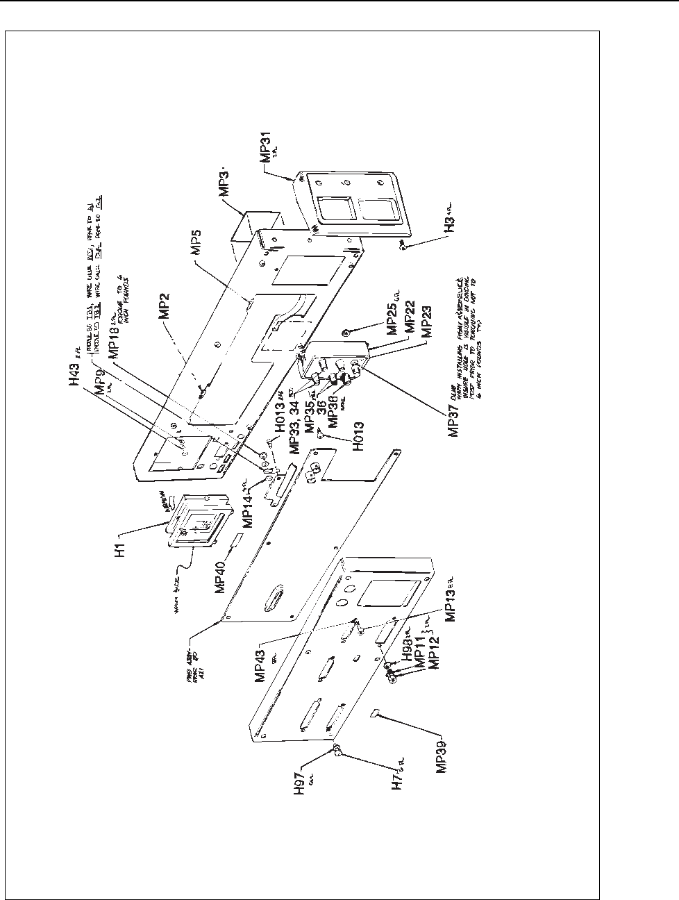
List of Replaceable Parts
Service Centers
6
6-11
5700A-T&B
f61b.eps
Figure 6-3. Rear Panel Final Assembly

5700A/5720A Series II Calibrator
Service Manual
6-12
Table 6-2. A1 Keyboard PCA
Reference
Designator Description Fluke Stock
No Tot Qty Notes
CR1-4 LED,GREEN,SUBMINIATURE 912241 4
DT1, DT2 * ISOLATOR,OPTO,OPTICAL SWITCH,INFRARED 523530 2
W1 CABLE, KEYBOARD/REAR PANEL 791657 1
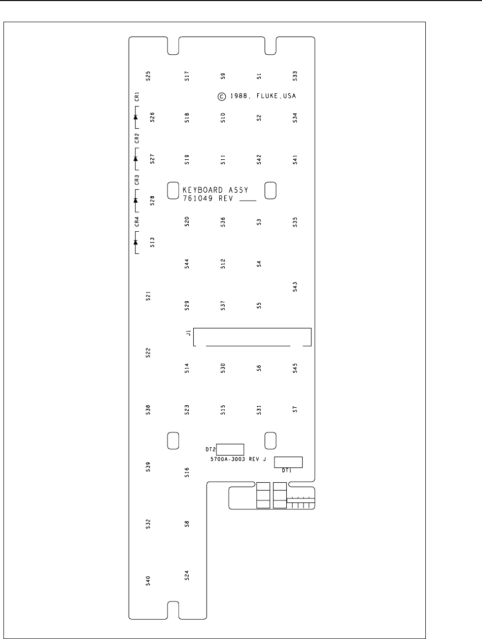
List of Replaceable Parts
Service Centers
6
6-13
5700A-1603
57001603.EPS
Figure 6-4. A1 Keyboard PCA

5700A/5720A Series II Calibrator
Service Manual
6-14
Table 6-3. A2 Front Panel PCA
Reference
Designator Description Fluke Stock
No Tot Qty Notes
C1, C2 CAP,TA,47UF,+-20%,10V 746990 2
C4,C9-20,C28,
C30,C35,C37,
C39-046,C64
CAP,CER,0.1UF,+-10%,25V,X7R,1206 747287
747287
747287
26
C3,C21-27,C29,
C31,C36,C38,
C47-50,C66
CAP,TA,10UF,+-20%,25V,6032 927814
927814
927814
17
C5,C33,C65 CAP,TA,1.5UF,+-20%,50V,6032 929302 3
C6,C8,C32,C34,
C51-54
CAP,CER,0.01UF,+-20%,100V,X7R,1206 742981 8
C7 CAP,AL,10UF,+-20%,100V,SOLV PROOF 820738 1
C55-59,C061,C62 CAP,POLYES,0.68UF,+-20%,100V 912506 7
C60 CAP,POLYES,0.68UF,+-20%,100V 912506 1
C63 CAP,CER,100PF,+-10%,50V,C0G,1206 740571 1
DS1 TUBE, DISPLAY, VAC FLOR,2-ROW,22-CHAR 806976 1
DS2 TUBE,DISPLAY,VAC FLUOR,256X26 832543 1
H1 LABEL,C-MOS INSTRUCTION 464016 1
J2 HEADER,2 ROW,.100CTR,40 PIN 807453 1
M1-10 FOOT,RUBBER,ADHES,BLK,.50 SQ,.12 THK 543488 10
Q1-4,Q7-10 * TRANSISTOR,SI,PNP,50V,350MW,SOT-23 742023 8
Q5,Q6,Q11,Q12 * TRANSISTOR,SI,NPN,50V,350MW,SOT-23 742031 4
R1,R3,R5,R6,R8,
R10-12,R20,R28-
R30,R55-59,R61,
R63,R65,R72, R76
*
*
*
*
*
RES,CERM,4.7K,+-5%,.125W,200PPM,1206 740522
740522
740522
740522
22
R2,R4,R7,R9,
R40,R41,R52, R53
*
*
*
RES,CERM,1.1K,+-5%,.125W,200PPM,1206 746008
746008
746008
8
R13-15,R24,R25,
R70,R73-75
*
*
RES,CERM,39K,+-5%,.125W,200PPM,1206 746677
746677
9
R16-19 * RES,CERM,150,+-1%,.125W,100PPM,1206 772780 4
R22,R26,R39,
R42,R51,R54
*
*
RES,CERM,6.8K,+-5%,.125W,200PPM,1206 746024
746024
6
R23,R27,R71 * RES,CERM,82K,+-5%,.125W,200PPM,1206 811794 3
R31-34,R43-46,
R60,R62,R64, R66
*
*
*
RES,CERM,1K,+-5%,.125W,200PPM,1206 745992
745992
745992
12
R35,R36,R68 * RES,CERM,620,+-5%,.125W,200PPM,1206 745984 3
R37,R38 * RES,CERM,470,+-5%,.125W,200PPM,1206 740506 2
R47,R48 * RES,CERM,453,+-1%,.125W,100PPM,1206 801415 2
R49,R50 * RES,CERM,1.5K,+-5%,.125W,200PPM,1206 746438 2
R67 * RES,CERM,200,+-5%,.125W,200PPM,1206 746339 1
R77 * RES,CERM,91,+-5%,.125W,200PPM,1206 756338 1
R81,R82 * RES,CERM,10,+-5%,1W,200PPM,2512 886705 2
R83 * RES,CERM,200,+-5%,.5W,200PPM,2010 886952 1
SP1 AF TRANSD,PIEZO,22 MM 602490 1
U1,U2 * IC,NMOS,1K X 8 DUAL PORT SRAM,PLCC 806653 2
U3 * IC,CMOS,PLD,PROGRAMD,5700A-90720,PLCC 838607 1
U4 * IC,CMOS,PLD,PROGRAMD,5700A-90721,PLCC 838615 1
U5 * IC,CMOS,PLD,PROGRAMD,5700A-90722,PLCC 845375 1
U6 * IC,CMOS,14 STAGE BINARY COUNTEER,SOIC 831081 1
U7 * IC,COMPARATOR,DUAL,HIGH SPEED,SOIC 831271 1
U8 * IC,CMOS,12 STAGE BIN RIPPLE CNTR,SOIC 831636 1
U9 * IC,CMOS,PLD,PROGRAMD,5700A-90723,PLCC 845383 1
U10 * IC,LSTTL,OCTL D TRNSPRNT LATCHES,SOIC 742726 1
U11 * IC,CMOS,HEX INVERTER,SOIC 742585 1

List of Replaceable Parts
Service Centers
6
6-15
Table 6-3. A2 Front Panel PCA (cont)
Reference
Designator Description Fluke Stock
No Tot Qty Notes
U12 * IC,CMOS,DUAL D F/F,+EDG TRG,SOIC 782995 1
U13 * IC,TTL,HEX INVERTER,W/OPEN COLL,SOIC 741249 1
U14-23 * IC,BIMOS,DISPLAY DRIVER,80V,PLCC 741231 10
U24 * IC,CMOS,PLD,PROGRAMD,5700A-90724,PLCC 837369 1
VR3,VR4 * ZENER,UNCOMP,6.2V,5%,60.5MA,1.5W,SMB 886700 2
VR5 * ZENER,UNCOMP,5.1V,5%,20MA,0.2W,SOT-23 837179 1
W1 CABLE, MOTHERBOARD TO DISPLAY 802694 1

5700A/5720A Series II Calibrator
Service Manual
6-16
5700A-1602
57001602.EPS
Figure 6-5. A2 Front Panel PCA

List of Replaceable Parts
Service Centers
6
6-17
Table 6-4. A3 Analog Motherboard PCA
Reference
Designator Description Fluke Stock
No Tot Qty Notes
C1 CAP,POLYES,0.1UF,+-10%,50V 649913 1
C2 CAP,CER,1000PF,+-20%,50V,X7R 697458 1
C3 CAP,TA,1UF,+-20%,35V 697417 1
C4 CAP,TA,4.7UF,+-20%,25V 807644 1
C5 CAP,POLYES,0.47UF,+-10%,50V 697409 1
CR1,CR2 * DIODE,SI,BV=75V,IO=150MA,500MW 203323 2
H1,H2 SCREW,PH,P,LOCK,STL,6-32,.250 152140 2
H3-5 CABLE ACCESS,TIE,4.00L,.10W,.75 DIA 172080 3
J101,J111,J201,
J202,J211,J212,
J301,J302,J311,
J312,J401,J402,
J501,J502,J511,
J512,J601,J602,
J611,J612,J701,
J702,J801,J802,
J901,J902
CONN,DIN41612,TYPE C,64 SCKT 807818
807818
807818
807818
807818
807818
807818
807818
807818
26
J71 FIBER OPTIC,RECEIVER,1MBD 822148 1
J72 FIBER OPTIC,TRANSMITTER,1MBD 822155 1
J811,J812,J821,
J822
SOCKET,1 ROW,PWB,.156CTR,10 POS 851183
851183
4
K1-3 RELAY,ARMATURE,2 FORM C,4.5VDC 783746 3
K4,K5,K9, K10 RELAY,REED,1 FORM A,5VDC 806950 4
K6-8,K11 RELAY,ARMATURE,2 FORM C,5V 733063 4
K12 RELAY,REED,1 FORM B,5VDC 845164 1
K13 RELAY,ARMATURE,2 FORM C,5V,LATCH 769307 1
MP3-54 RIVET,S-TUB,OVAL,AL,.087,.250 838482 52
MP55,MP56 SPACER,BROACH,.281 RND,STL,6-3 414508 2
MP57-61 SPACER,BROACH,SNAP,BR,.250 820613 5
MP62-66 CLAMP,CABLE,ADHESIVE,NYLON,.125 854273 5
MP101-128 CONN ACC,DIN41612,KEY 832733 28
R1 RES,CF,75,+-5%,0.25W 441642 1
R2 RES,CF,91,+-5%,0.25W 441683 1
RV1 VARISTOR,22V,+-20%,1.0MA 500777 1
W1 CABLE, FRONT/REAR 802835 1
W2 CABLE ASSY, MOTHERBOARD BUS, FRONT 859926 1
W3 CABLE ASSY, MOTHERBOARD BUS, REAR 859934 1
W8 CABLE, KEYBOARD/REAR PANEL 802710 1
W11 CABLE, BOOST 802744 1
XK1-3 RELAY SOCKET,4 POLE 441964 3
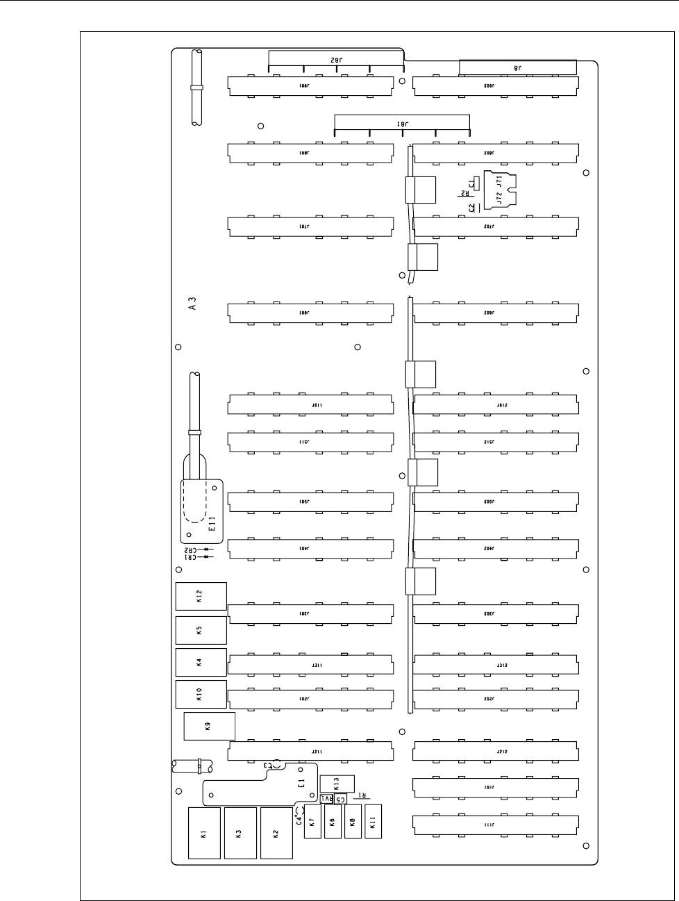
5700A/5720A Series II Calibrator
Service Manual
6-18
5700A-1601
57001601.EPS
Figure 6-6. A3 Analog Motherboard PCA

List of Replaceable Parts
Service Centers
6
6-19
Table 6-5. A4 Digital Motherboard PCA
Reference
Designator Description Fluke Stock
No Tot Qty Notes
C1,C4 CAP,TA,10UF,+-20%,35V 816512 2
C2 CAP,CER,1000PF,+-20%,50V,X7R 697458 1
C3 CAP,POLYES,0.1UF,+-10%,50V 649913 1
C5 CAP,POLYES,0.1UF,+-20%,250VAC 542233 1
C6 CAP,CER,6800PF,+-5%,100V,C0G 816710 1
CR3,CR4 DIODE,SI,100 PIV,1.0 AMP 698555 2
F1 FUSE,.25X1.25,3A,250V,SLOW 109280 1 1
H8-14 CABLE ACCESS,TIE,4.00L,.10W,.75 DIA 172080 7
H19,H20 SCREW,PH,P,LOCK,SS,4-40,.187 149567 2 2
H21,H22 WASHER,FLAT,STL,.093,.219,.020 306415 2
J11 HEADER,1 ROW,.156CTR,12 PIN 813362 1
J13 HEADER,1 ROW,.156CTR,10 PIN 446724 1
J14 HEADER,1 ROW,.156CTR,16 PIN 831370 1
J15 HEADER,1 ROW,.156CTR,14 PIN 831362 1
J16 HEADER,1 ROW,.156CTR,8 PIN 385435 1
J21 CONN,DIN41612,TYPE C,RT ANG,64 PIN 853437 1
J31 HEADER,1 ROW,.156CTR,RT ANG,5 PIN 844717 1
J41,J61,J62 CONN,DIN41612,TYPE C,64 SCKT 807818 3
J51,J52 HEADER,1 ROW,.100CTR,3 PIN 845334 2
J73 FIBER OPTIC,TRANSMITTER,1MBD 822155 1
J74 FIBER OPTIC,RECEIVER,1MBD 822148 1
J91 HEADER,2 ROW,.100CTR,34 PIN 851696 1
MP1 HLDR PART,FUSE,BODY,PWB MT 602763 1
MP2 HLDR PART,FUSE,CAP,1/4X1-1/4 460238 1
MP3-10 RIVET,S-TUB,OVAL,AL,.087,.250 838482 8
MP11 RIVET,S-TUB,OVAL,AL,.087,.343 838458 2
MP16 BRACKET, POWER SWITCH 885710 1 2
MP17,MP18,
MP20
SPACER,SWAGED,.312 RND,BR,.177 837864
837864
3
MP22,MP23 FOOT,RUBBER,ADHES,GRY,.44 DIA,.20 THK 1601870 2
MP24-26 SPACER,BROACH,SNAP,AL,.187 820639 3
P81,P82 HEADER,1 ROW,.156CTR,20 PIN 831222 2
R1 RES,CF,91,+-5%,0.25W 441683 1
R2,R3 RES,WW,2,+-1%,.7W 255646 2
R4 RES,CF,68,+-5%,0.25W 414532 1
RV1 VARISTOR,22V,+-20%,1.0MA 500777 1
RV2 VARISTOR,430V,+-10%,1.0MA 519355 1
SW1 SWITCH,PUSHBUTTON,DPST,PUSH-PUSH 665513 1 2
SW2-4 SWITCH,SLIDE,DPDT,LINE SELECT,RT ANG 817353 3
W15 CABLE, FIBER OPTIC 802769 1
W90 CABLE, REAR PANEL-CPU 802728 1
1. Fuse PN 109280 is for 100-120 volt configuration. For 200-230 volt configuration order PN 109231.
2. 3 parts make up assembly 665513
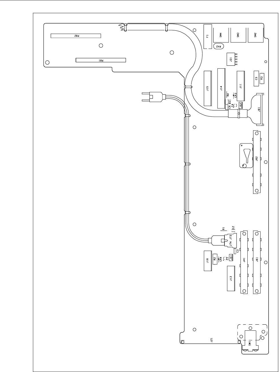
5700A/5720A Series II Calibrator
Service Manual
6-20
5700A-1605
57001605.EPS
Figure 6-7. A4 Digital Motherboard PCA

List of Replaceable Parts
Service Centers
6
6-21
Table 6-6. A5 Wideband Output PCA, Option -03
Reference
Designator Description Fluke Stock
No Tot Qty Notes
C1 CAP,CER,4.7PF,+-0.25PF,50V,C0G 721837 1
C2 CAP,CER,22PF,+-2%,50V,C0G 714832 1
C3 CAP,POLYES,0.047UF,+-10%,50V 820548 1
C4,C11-13,C66 CAP,CER,100PF,+-5%,50V,C0G 831495 5
C5 CAP,CER,470PF,+-10%,50V,C0G 733071 1
C6,C52,C53,C79 CAP,POLYES,0.033UF,+-10%,50V 715276 4
C14 CAP,POLYES,0.22UF,+-5%,50V 747519 1
C7,C10,C15,C23,
C81
CAP,POLYES,0.47UF,+-10%,50V 697409
697409
5
C8,C9,C25,C27-
29,C33-37,C45-
51,C55-63,C72-
76,C80,C30,C31
CAP,POLYES,0.1UF,+-10%,50V 649913
649913
649913
649913
36
C16,C18,C26,
C39-44,C32
CAP,TA,4.7UF,+-20%,25V 807644
807644
10
C17,C21 CAP,TA,4.7UF,+-20%,25V 807644 2
C19,C77,C78 CAP,POLYES,0.001UF,+-10%,50V 720938 3
C20,C22, CAP,CER,33PF,+-5%,50V,C0G 714543 2
C38 CAP,CER,5.6PF,+-0.25PF,100V,C0H 512954 1
C64,C65 CAP,POLYES,1UF,+-10%,50V 733089 2
C67 CAP,CER,33PF,+-2%,50V,C0G 715292 1
C68 CAP,CER,18PF,+-2%,100V,C0G 830638 1
C82 CAP,AL,47UF,+-20%,16V,SOLV PROOF 643304 1
C83 CAP,CER,270PF,+-5%,50V,C0G 658898 1
CP1 ADAPTER,BNC(F),BANANA PLUG(M) 528802 1
CP2 ADAPTER,COAX,BNC(M),N(F) 756775 1
CP3 POUCH,TEST LEAD 525212 1
CR1-4,CR6,CR7 * DIODE,SI,BV=75V,IO=150MA,500MW 659516 6
CR5 * I-REG DIODE,5.3MA,21%,SEL,TO-226AC 852116 1
E1,E2 WIRE,COPPER/TIN,BUS,22AWG 115469 2
E3, JUMPER,REC,2 POS,.100CTR,.025 757294 1
H1 LABEL,C-MOS INSTRUCTION 464016 1
H7-9 SCREW,PH,P,LOCK,SS,6-32,.500 320051 4
H10-19 INSUL PT,TRANSISTOR MOUNT,DAP,TO-5 152207 10
J1,J2 CONN,COAX,SMB(M),PWB,RT ANG 353243 2
J3 HEADER,1 ROW,.100CTR,2 PIN 643916 1
K1,K11 RELAY,ARMATURE,4 FORM C,5V,LATCH 715078 2
K2,K3,K9,K10, K12 RELAY,ARMATURE,2 FORM C,5V,LATCH 769307 5
K4-8 RELAY,ARMATURE,2 FORM C,5VDC 806810 5
L1-6,L18,L123-128 CHOKE,6TURN 320911 7 1
L19 INDUCTOR,100UH,+-10%,12MHZ,SHLD 249102 1
L20-22 INDUCTOR,220UH,+-5%,9.4MHZ,SHLD 147835 3
L23 CORE,TOROID,FERRITE,.047X.138X.118 321182 1
M2 SHIELD, WB OUTPUT, REAR 764498 1
M3 SHIELD, WIDEBAND AMP, FRONT 775643 1
M4 SHIELD, WB OUTPUT, ATTENUATOR,REAR 775650 1
M5 SHIELD, WB OUTPUT, ATTENUATOR,FRONT 775668 1
MP1 TERMINATION,COAX,N(M),N(F),50 OHM 853429 1
MP2,MP3 RIVET,S-TUB,OVAL,AL,.087,.343 838458 2
MP4,MP5 EJECTOR,PWB,NYLON 494724 2
MP6,MP25-34 SCREW,PH,P,LOCK,STL,6-32,.250 152140 11
MP10-14 RELAY WASHER 803247 5
MP15-24 HEAT DIS,PRESS ON,TO-5 418384 10
P111 CONN,DIN41612,TYPE C,RT ANG,64 PIN 807800 1
Q1 * TRANSISTOR,SI,NPN,SMALL SIGNAL 698241 1
1. L123, L124- alternate PN 452888 if there is difficulty meeting 30 MHz specificaiton

5700A/5720A Series II Calibrator
Service Manual
6-22
Table 6-6. A5 Wideband Output PCA, Option -03 (cont)
Reference
Designator Description Fluke Stock
No Tot Qty Notes
Q17 * TRANSISTOR,SI,N-JFET,TO-92 816314 1
Q2,Q03 * TRANSISTOR,SI,N-DMOS FET,TO-72 394122 2
Q4-6 * TRANSISTOR,SI,NPN,20V,500MW,MACRO-T 659417 3
Q7,Q8 * PNP,2N5583 ,TRANSISTOR,SI,PNP,30V,5W,TO-39 800201 2
Q9,Q10 * TRANSISTOR,SI,NPN,ST1020,60V,500MA,1GHZ,3W,TO-39 1590835 2
Q11-13 * TRANSISTOR,SI,PNP,ST2525A,60V,500MA,1.3GHZ,5W,TO-39 1575948 2
Q14-16 * TRANSISTOR,SI,NPN,ST1020,60V,500MA,1GHZ,3W,TO-39 1590835 2
Q18 * TRANSISTOR,SI,N-DMOS PWR FET,T0-92 782565 1
R1 RES,MF,866,+-1%,0.125W,50PPM 320390 1
R2 RES,MF,200,+-1%,0.125W,100PPM 245340 1
R3 RES,MF,412K,+-1%,0.125W,50PPM 714287 1
R7,R8 RES,MF,698K,+-1%,0.125W,100PPM 757252 2
R9,R24,R27,R42,
R102
RES,CF,20K,+-5%,0.25W 697110
697110
5
R10 RES,CF,3M,+-5%,0.25W 746172 1
R11 RES,MF,20.5K,+-1%,0.125W,100PPM 655233 1
R12,R111-113 RES,CF,2K,+-5%,0.25W 810457 4
R13 RES,MF,14.3K,+-1%,0.125W,100PPM 721803 1
R14,R28,R114 RES,MF,10K,+-1%,0.125W,100PPM 658914 3
R15,R38 RES,CF,3K,+-5%,0.25W 810366 2
R16 RES,CF,620,+-5%,0.25W 810408 1
R17 RES,MF,866,+-1%,0.125W,50PPM 816603 1
R18 RES,MF,200,+-1%,0.125W,100PPM 820282 1
R19, RES,CF,12K,+-5%,0.25W 757799 1
R20,R31 RES,CF,4.7K,+-5%,0.25W 721571 2
R21,R104 RES,MF,10.5K,+-1%,0.125W,100PPM 816611 2
R22,R35 RES,CF,9.1K,+-5%,0.25W 706663 2
R23 RES,CF,1M,+-5%,0.25W 649970 1
R25 RES,MF,205K,+-1%,0.125W,100PPM 706234 1
R26 RES,CF,43K,+-5%,0.25W 821777 1
R29,R121 RES,MF,56.2K,+-1%,0.125W,100PPM 706242 2
R30,R103,R105,
R106
RES,CF,150K,+-5%,0.25W 758219
758219
4
R32,R63 RES,CF,10K,+-5%,0.25W 697102 2
R33 RES,CF,22K,+-5%,0.25W 747535 1
R34 RES,CF,24K,+-5%,0.25W 697599 1
R36,R40,R45, R62 RES,CF,1K,+-5%,0.25W 780585
780585
4
R37 RES,MF,210,+-1%,0.125W,100PPM 327999 1
R39 RES,CF,16K,+-5%,0.25W 714303 1
R41 RES,CF,180K,+-5%,0.25W 348946 1
R43,R44 RES,MF,100,+-0.1%,0.125W,25PPM 357400 2
R46 RES,MF,1.74K,+-1%,0.125W,100PPM 344358 1
R47 RES,MF,1K,+-1%,0.125W,100PPM 168229 1
R48,R49,R51,
R55,R61,R65,
R71,R76,R77,
R84,R85,R90, R91
RES,CF,51,+-5%,0.25W 414540
414540
414540
414540
414540
13
R50 RES,MF,499,+-1%,,0.125W,100PM 168211 1
R52 RES,MF,150,+-1%,0.125W,100PPM 448555 1
R53 RES,MF,402,+-1%,0.125W,100PPM 289611 1
R54 RES,MF,576,+-1%,0.125W,100PPM 294843 1
R56,R57 RES,MF,80.6,+-1%,0.5W,100PPM 158790 2
R58,R59 RES,MF,75,+-1%,0.5W,100PPM 150870 2
R64 RES,MF,806,+-1%,0.6W,50PPM 851944 1
R66 RES,MF,49.9,+-1%,0.125W,100PPM 305896 1
R67,R68 RES,MF,21,+-1%,0.125W,100PPM 296632 2

List of Replaceable Parts
Service Centers
6
6-23
Table 6-6. A5 Wideband Output PCA, Option -03 (cont)
Reference
Designator Description Fluke Stock
No Tot Qty Notes
R69,R70 RES,MF,249,+-1%,0.5W,100PPM 241281 2
R72,R73,R80-83 RES,MF,909,+-1%,0.5W,100PPM 178053 6
R74 RES,CF,20K,+-5%,0.25W 441477 1
R75 RES,MF,10K,+-1%,0.125W,100PPM 168260 1
R78,R79,R86-89 RES,MF,12.7,+-1%,0.125W,100PPM 441766 6
R92-95 RES,MF,75,+-1%,0.125W,100PPM 306027 4
R96-99 RES,MF,187,+-0.1%,0.5W,25PPM 807750 4
R100 RES,MF,1.21K,+-1%,0.125W,100PPM 229146 1
R101 RES,MF,1.43K,+-1%,0.125W,25PPM 447995 1
R107 RES,CF,100,+-5%,0.25W 810465 1
R108 RES,MF,49.9,+-1%,0.125W,100PPM 820266 1
R109 RES,MF,2.15K,+-1%,0.125W,50PPM 347039 1
R110 RES,MF,1K,+-0.1%,0.125W,25PPM 340380 1
R115 RES,CF,200K,+-5%,0.25W 441485 1
R116 RES,MF,2K,+-1%,0.125W,100PPM 816629 1
R117 RES,MF,1.69K,+-1%,0.125W,100PPM 321414 1
R118 RES,CF,1.5K,+-5%,0.25W 810432 1
R119 RES,MF,8.06K,+-1%,0.125W,100PPM 817619 1
R120 RES,MF,124,+-1%,0.125W,100PPM 343905 1
R122 RES,MF,4.99K,+-1%,0.125W,100PPM 721548 1
TP1-19 JUMPER,WIRE,NONINSUL,0.200CTR 816090 19
U1 * RMS CONVERTER TESTED 400 OHM-B 842591 1
U2,U12 * IC,OP AMP,DUAL,PRECISION,8-PIN 783696 2
U3 * IC,ARRAY,5 TRANS,NPN,3 ISO,2 DIFF CON 248906 1
U4 * IC,COMPARATOR,DUAL,LO-PWR,8 PIN DIP 478354 1
U5 * IC,OP AMP,LO-OFFSET VOLTAGE,LO-NOISE 605980 1
U6 * IC,BIMOS,8 CHNL HI-VOLT DRVR W/LATCH 782912 1
U7 * IC,CMOS,PROGRMBL PERIPHERAL INTERFACE 780650 1
U8 * IC,CMOS,8-1 LINE MUX/DEMUX ANALOG SW 836304 1
U9,U10 * IC,BIMOS,4 CHNL HI-VOLT DRVR W/LATCH 820514 2
U11 * IC,OP AMP,DUAL,LO OFFST VOLT,LO-DRIFT 851704 1
VR1 * ZENER,UNCOMP,9.1V,5%,20MA,0.5W 853788 1
VR2 * ZENER,COMP,6.4V,2%,2PPM,1MA 419036 1
VR3 * ZENER,UNCOMP,16.0V,5%,15.5MA,1.0W 313221 1
VR4 * ZENER,UNCOMP,5.6V,5%,20MA,0.5W 277236 1
W1 CABLE, WIDEBAND OUTPUT INTERCONNECT 802876 1
W2 CABLE ASSY,50 OHM,COAX,N(M),3FT 853432 1
Z1 * RNET,CERM,SIP 5700 ATTENUATOR 760728 1
Z2 * RNET,CERM,SIP,5700 ATTENUATOR 760769 1

5700A/5720A Series II Calibrator
Service Manual
6-24
5700A-1611
57001611.EPS
Figure 6-8. A5 Wideband Output PCA, Option -03

List of Replaceable Parts
Service Centers
6
6-25
Table 6-7. A6 Wideband Ocillator PCA, Option -03
Reference
Designator Description Fluke Stock
No Tot Qty Notes
C1-8,C49-51 CAP,TA,4.7UF,+-20%,25V 807644 11
C9,C10 CAP,CER,2700PF,+-5%,50V,C0G 832303 2
C11 CAP,CER,15PF,+-20%,50V,C0G 697524 1
C12,C15,C16,
C18-25,C29-33,
C35-48,C52,
C57,C58,C60,
C61,C101,C103,
C105-107,C201,
C203,C205-207,
C301,C303, C305-
307,C401,
C403,C405-407,
C501,C503,C505-
507
CAP,POLYES,0.1UF,+-10%,50V 649913
649913
649913
649913
649913
649913
649913
649913
649913
649913
649913
649913
55
C13,C14 CAP,CER,0.047UF,+-10%,100V,X7R 844733 2
C17 CAP,POLYES,0.22UF,+-10%,50V 706028 1
C26-28 CAP,CER,0.01UF,+-10%,100V,X7R 557587 3
C34,C209-212 CAP,CER,82PF,+-2%,50V,C0G 714857 5
C53 CAP,CER,6800PF,+-5%,50V,C0G 542894 1
C54,C55,C102,
C108,C202,C208,
C302,C308,C402,
C408,C502,C508
CAP,POLYES,0.001UF,+-10%,50V 720938
720938
720938
720938
12
C56,C59 CAP,CER,33PF,+-5%,50V,C0G 714543 2
C62,C409-412 CAP,CER,390PF,+-2%,50V,C0G 820530 5
C109-112 CAP,CER,47PF,+-2%,100V,C0G 832295 4
C309-312 CAP,CER,180PF,+-2%,50V,C0G 820522 4
C509-512 CAP,CER,820PF,+-2%,50V,C0G 631002 4
CR1,CR2 DIODE,SI,VARACTOR,PIV=28V,500PF 598078 2
CR102,CR103,
CR202,CR203,
CR302,CR303,
CR402,CR403,
CR502,CR503
*
*
*
*
*
DIODE,SI,SWICHING,PIN 334227
334227
334227
334227
334227
10
CR3-9 CR101,
CR201 CR301,
CR401 CR501
*
*
*
DIODE,SI,BV=75V,IO=150MA,500MW 659516
659516
659516
12
E2-5 JUMPER,WIRE,NONINSUL,0.200CTR 816090 4
E6 JUMPER,REC,2 POS,.100CTR,.025 757294 1
H6 LABEL,C-MOS INSTRUCTION 464016 1
H10 SCREW,PH,P,LOCK,SS,6-32,.750 376822 1
J1 CONN,COAX,SMB(M),PWB,RT ANG 353243 1
J6 HEADER,1 ROW,.100CTR,2 PIN 643916 1
L1-4,L7-12,L14,
L15
CHOKE,6TURN 320911
320911
12
L5 INDUCTOR,0.20UH,+-10%,400MHZ,SHLD 886809 1
L6 INDUCTOR,1500UH,+-5%,2.5MHZ,SHLD 806505 1
L16,L102,L104 INDUCTOR,1UH,+-5%,156MHZ,SHLD 806562 3
L101,L503 INDUCTOR,22UH,+-10%,38MHZ,SHLD 147843 2
L103 INDUCTOR,1.5UH,+-5%,128MHZ,SHLD 413856 1
L201 INDUCTOR,33UH,+-10%,33MHZ,SHLD 249086 1
L202,L204 INDUCTOR,2.2UH,+-5%,108MHZ,SHLD 806547 2
L203 INDUCTOR,3.3UH,+-10%,88MHZ,SHLD 174714 1
L301 INDUCTOR,82UH,+-10%,14MHZ,SHLD 542290 1
L302,L304 INDUCTOR,3.9UH,+-5%,84MHZ,SHLD 413864 2
L303 INDUCTOR,5.6UH,+-10%,69MHZ,SHLD 598219 1
L401 INDUCTOR,120UH,+-5%,11.2MHZ,SHLD 321042 1
L402,L404 INDUCTOR,8.2UH,+-5%,58MHZ,SHLD 806521 2

5700A/5720A Series II Calibrator
Service Manual
6-26
Table 6-7. A6 Wideband Ocillator PCA, Option -03 (cont)
Reference
Designator Description Fluke Stock
No Tot Qty Notes
L403 INDUCTOR,12UH,+-5%,47MHZ,SHLD 820720 1
L501 INDUCTOR,220UH,+-5%,9.4MHZ,SHLD 147835 1
L502,L504 INDUCTOR,15UH,+-5%,41MHZ,SHLD 806513 2
MP1 SHIELD, WIDEBAND OSCILLATOR, FRONT 775478 1
MP2 SHIELD, WIDEBAND OSCILLATOR, REAR 775486 1
MP5,MP11,MP12 CABLE ACCESSORY,CLAMP,ADHESIVE 838300 3
MP6,MP7 RIVET,S-TUB,OVAL,AL,.087,.343 838458 2
MP8,MP9 EJECTOR,PWB,NYLON 494724 2
MP10 CABLE, 75 OHM RF 761304 1
P101 CONNECTOR ,CONN,DIN41612,TYPE C,RT ANG,64 PIN 807800 1
Q2,Q3 TRANSISTOR,SI,NPN,SMALL SIGNAL 698241 2
Q4-7 * TRANSISTOR,SI,NPN,HI-FREQ,SMALL 659417 4
Q8,Q9,Q101,
Q105,Q201,Q205,
Q301,Q305,Q401,
Q405 Q501,Q505
*
*
*
*
TRANSISTOR,SI,N-DMOS FET,TO-72 394122
394122
394122
394122
12
Q102,Q202,Q302,
Q402,Q502
*
*
TRANSISTOR,SI,NPN,HI FREQ,TO-39 912522
912522
5
Q103,Q104,Q203,
Q204,Q303,Q304,
Q403,Q404,Q503,
Q504
*
*
*
*
TRANSISTOR,SI,NPN,SMALL SIGNAL 820407
820407
820407
820407
10
R3 RES,CF,300K,+-5%,0.25W 732818 1
R4,R5,R39,R41 RES,CF,12K,+-5%,0.25W 757799 4
R6,R87 RES,CF,100,+-5%,0.25W 810465 2
R7 RES,CF,9.1K,+-5%,0.25W 706663 1
R8,R25-27,R38,
R52,R66,R67,
R79,R80,R83
RES,CF,1K,+-5%,0.25W 780585
780585
780585
11
R9 RES,CF,20K,+-5%,0.25W 697110 1
R11,R12 R15-18,
R21,R22
RES,CF,51,+-5%,0.25W 414540
414540
8
R13,R14,R19,
R20,R23,R24, R70
RES,CF,270,+-5%,0.25W 348789
348789
348789
7
R28-30,R36,R81 RES,CF,2K,+-5%,0.25W 810457 5
R31 RES,MF,7.32K,+-1%,0.125W,100PPM 853630 1
R32,R53 RES,MF,1K,+-1%,0.125W,100PPM 816595 2
R33,R42,R43,
R46,R50,R54,
R60,R86,R103,
R203,R303,R403,
R503
RES,MF,49.9,+-1%,0.125W,100PPM 820266
820266
820266
820266
820266
13
R34,R57 RES,MF,30.1,+-1%,0.125W,100PPM 820563 2
R35,R55 RES,MF,3.32K,+-1%,0.125W,100PPM 817601 2
R37 RES,CF,3.9K.+-5%,0.25W 810416 1
R40,R74-78,R102,
R110,R111, R113-
116,R202,R210,
R211,R213-216,
R302,R310,R311,
R313,R402,R410,
R411,R413,R502,
R510,R511, R513
RES,CF,10K,+-5%,0.25W 697102
697102
697102
697102
697102
697102
697102
697102
32
R44 RES,CF,4.7K,+-5%,0.25W 721571 1
R45,R47 RES,MF,200,+-1%,0.125W,100PPM 820282 2
R48 RES,MF,866,+-1%,0.125W,50PPM 816603 1
R49 RES,MF,10K,+-1%,0.125W,100PPM 658914 1
R51 RES,MF,4.99K,+-1%,0.125W,100PPM 721548 1
R56 RES,CC,330,+-5%,0.5W 686789 1
List of Replaceable Parts
Service Centers
6
6-27
Table 6-7. A6 Wideband Ocillator PCA, Option -03 (cont)
Reference
Designator Description Fluke Stock
No Tot Qty Notes
R58,R112,R212,
R312,R412,R512
RES,MF,110,+-1%,0.125W,100PPM 820571
820571
6
R59 RES,MF,14.3K,+-1%,0.125W,100PPM 721803 1
R61 RES,MF,2.49K,+-1%,0.125W,100PPM 810523 1
R62,R64,R65,R69 RES,CC,680,+-5%,0.5W 687803 4
R63 RES,CF,200,+-5%,0.25W 810390 1
R68 RES,MF,1.62K,+-1%,0.125W,100PPM 772004 1
R71 RES,MF,75,+-1%,0.125W,100PPM 820241 1
R72,R73 RES,MF,6.65K,+-0.1%,0.125W,100PPM 772558 2
R82 RES,CF,6.2K,+-5%,0.25W 714337 1
R84,R85 RES,CF,240,+-5%,0.25W 830588 2
R101,R201,R301,
R401,R501
RES,CC,220,+-5%,0.5W 643442
643442
5
R104,R204,R304,
R404,R504
RES,MF,249,+-1%,0.5W,100PPM 241281
241281
5
R105,R205,R305,
R405,R505
RES,MF,100,+-1%,0.125W,100PPM 817627
817627
5
R106,R107,R206,
R207,R306,R307,
R406,R407,R506,
R507
RES,CF,130,+-5%,0.25W 817593
817593
817593
817593
10
R108,R208,R308,
R408,R508
RES,MF,523,+-1%,0.125W,100PPM 820274
820274
5
R109,R209,R309,
R409,R509
RES,MF,2.67K,+-1%,0.125W,100PPM 820290
820290
5
TP1-4,TP10-17 JUMPER,WIRE,NONINSUL,0.200CTR 816090 11
U1 * IC,CMOS,4-BIT PHASE LCKD LOOP 799452 1
U2 * IC,OP AMP,JFET INPUT,8 PIN DIP 472779 1
U3 * IC,ECL,VOLTAGE CONTROLLED OSCILLATOR 454975 1
U4 * IC,ECL,DUAL D M/S F/F,W/SET&RESET 454959 1
U5 * IC,ECL,4-BIT BINARY COUNTER,12MHZ 799460 1
U6 * IC,ECL,8-1 LINE MULTIPLEXER (MUX) 799510 1
U7,U10,U11 * IC,COMPARATOR,QUAD,14 PIN DIP 387233 3
U8 * IC,CMOS,BCD-DEC & BIN-OCTAL DC 473769 1
U9 * IC,PBLR,MONOLITHIC,DIFF. AMP 783738 1
U12,U13 * IC,ARRAY,5 TRANS,NPN,5 ISOLATE 380188 2
U14 * IC,CMOS,QUAD INPUT NOR GATE 811158 1
U15 * IC,COMPARATOR,HI-SPEED,14 PIN 647115 1
VR1,VR4 * ZENER,UNCOMP,5.1V,5%,20.0MA,0.5W 853700 2
VR2,VR3 * ZENER,UNCOMP,10.0V,5%,20.0MA,05W 473744 2
VR5 * ZENER,UNCOMP,6.2V,5%,200MA,5W 806802 1
Z1 RES,CERM,SIP,10 PIN,9 RES,10K,+-2% 414003 1
Z2 RES,CERM,SIP,6 PIN,5 RES,10K,+-2% 500876 1
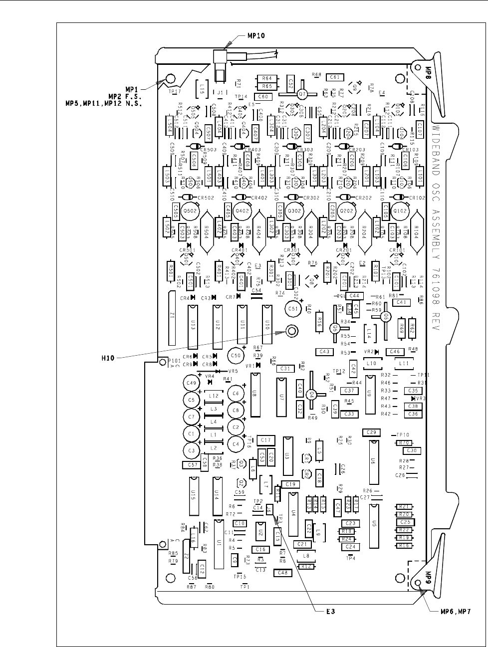
5700A/5720A Series II Calibrator
Service Manual
6-28
5700A-1610
57001610.EPS
Figure 6-9. A6 Wideband Oscillator PCA, Option -03

List of Replaceable Parts
Service Centers
6
6-29
Table 6-8. A7 Current/High-Res Oscillator PCA
Reference
Designator Description Fluke Stock
No Tot Qty Notes
C1,C71 CAP,CER,0.22UF,+80-20%,50V,Z5U 649939 2
C2,C3,C18-20,
C29,C32-35,C47,
C48,C50,C51,
C55,C56
CAP,POLYES,0.1UF,+-10%,50V 649913
649913
649913
649913
16
C4,C5 CAP,CER,100PF,+-2%,100V,C0G 812115 2
C6,C7,C21-24,
C37,C38,C40,
C43,C52,C53,
C60,C61
CAP,TA,4.7UF,+-20%,25V 807644
807644
807644
807644
14
C8 CAP,CER,18PF,+-2%,100V,C0G 830638 1
C9 CAP,CER,47PF,+-20%,50V,C0G 706705 1
C10 CAP,CER,470PF,+-5%,50V,C0G 830430 1
C11 CAP,CER,4700PF,+-20%,100V,C0G 743427 1
C12,C13,C70 CAP,AL,47UF,+-20%,50V,SOLV PROOF 822403 3
C14 CAP,AL,6.8UF,+-20%,35V,SOLV PROOF 643189 1
C15 CAP,TA,2.2UF,+-20%,16V 706804 1
C16 CAP,CER,1000PF,+-2%,50V,C0G 807966 1
C17,C45,C46, C54 CAP,CER,33PF,+-5%,50V,C0G 714543
714543
4
C25,C26,C30,
C36,C41,C42, C49
CAP,POLYES,0.047UF,+-10%,50V 820548
820548
820548
7
C27,C28 CAP,POLYES,1UF,+-10%,50V 733089 2
C31,C67 CAP,POLYES,0.22UF,+-5%,50V 747519 2
C39 CAP,TA,22UF,+-20%,25V 845149 1
C44 CAP,CER,15PF,+-20%,50V,C0G 697524 1
C57,C58 CAP,CER,2000PF,+-5%,50V,C0G 832618 2
C59 CAP,CER,390PF,+-2%,50V,C0G 820530 1
C62 CAP,CER,820PF,+-2%,50V,C0G 631002 1
C65,C66 CAP,CER,82PF,+-2%,100V,C0G 512350 2
C68 CAP,CER,150PF,+-5%,100V,C0G 512988 1
C69 CAP,CER,27PF,+-2%,100V,C0G 816652 1
CR1,CR2, CR10,
CR11
*
*
DIODE,SI,BV=125V,IO=150MA,500 MW 844647
844647
4
CR3,CR4 * DIODE,SI,BV=75V,IO=150MA,500MW 659516 2
CR9 DIODE,SI,VARACTOR,PIV=28V,500PF 598078 1
CR12,CR13 DIODE,SI,BV=200V,IO=200MA 876867 2
E1,E2 JUMPER,WIRE,NONINSUL,0.200CTR 816090 2
H1-4 RIVET,S-TUB,OVAL,AL,.087,.343 838458 4
HR2 * RN/HYBRID CURRENT HYBRID 775387 1
K1-3,K6 K7,K10-
13,K16
RELAY,ARMATURE,2 FORM C,5V,LATCH 769307
769307
10
K4,K5,K8,K9 RELAY,ARMATURE,4 FORM C,5V,LATCH 715078 4
K14,K15,K17 RELAY,ARMATURE,2 FORM C,5V 733063 3
L1-3,L5,L7-9 CHOKE,6TURN 320911 7
L4 INDUCTOR,3.3UH,+-10%,88MHZ,SHLD 174714 1
L10 INDUCTOR,1UH,+-5%,156MHZ,SHLD 806562 1
L11 INDUCTOR,150UH,+-5%,10.5MHZ,SHLD 174763 1
L12 INDUCTOR,6800UH,+-10%,1.5MHZ,SHLD 363184 1
MP1-5 HEAT DIS,PWB MT,.75X.50X.50,TO-220 816587 5 1,2
MP6 MOLDED COVER, HYBRID, R-NET 775619 1
MP7,MP8 SHIELD, HIGH RES, FRONT 775684 2
MP9,MP10 SHIELD, HIGH RES, REAR 764589 2
MP11,MP12 EJECTOR,PWB,NYLON 494724 2
P211,P212 CONN,DIN41612,TYPE C,RT ANG,64 PIN 807800 2
Q1 * TRANSISTOR,SI,BV=40V,40W,TO-22 665448 1 1

5700A/5720A Series II Calibrator
Service Manual
6-30
Table 6-8. A7 Current/High-Res Oscillator PCA (cont)
Reference
Designator Description Fluke Stock
No Tot Qty Notes
Q2,Q5,Q16,Q18 * TRANSISTOR,SI,NPN,SMALL SIGNAL 698225 4
Q3,Q4,Q19 * TRANSISTOR,SI,PNP,40V,0.35W,TO-92 698233 3
Q6,Q7 * TRANSISTOR,SI,BV=80V,10W,TO-20 495689 2
Q8,Q9 * TRANSISTOR,SI,BV=80V,10W,TO-20 535468 2
Q10,Q11 * TRANSISTOR,SI,BV=45V,27W,TO-22 325753 2 3
Q12,Q13 * TRANSISTOR,SI,BV=55V,30W,TO-22 325761 2 2
Q14,Q25 * TRANSISTOR,SI,BV=60V,65W,TO-22 386128 2
Q15 * TRANSISTOR,SI,NPN,SMALL SIGNAL 698241 1
Q17 * TRANSISTOR,SI,VMOS,PWR,TO-237,VM10KM 640516 1
Q20-23 * TRANSISTOR,SI,N-DMOS PWR FET,TO-92 782565 4
Q24 * TRANSISTOR, SI, BV=60V, 65W, T0-220 559989 1
R1,R38-40,R44,
R54,R55,R61,
R62,R65, R78, R91
RES,CF,1K,+-5%,0.25W 780585
780585
780585
780585
12
R3,R36 RES,CF,4.7K,+-5%,0.25W 721571 2
R4,R9,R81,R82,
R94
RES,MF,1K,+-1%,0.125W,100PPM 816595
816595
5
R5,R8 RES,CF,62K,+-5%,0.25W 713941 2
R6,R7 RES,MF,8.87K,+-1%,0.125W,100PPM 658922 2
R10,R12,R29, R32 RES,MF,8.25K,+-1%,0.125W,100PPM 820357
820357
4
R11,R13 RES,MF,909,+-1%,0.125W,100PPM 820308 2
R14 RES,WW,1.2,+-5%,2W 602182 1
R16 RES,CF,20K,+-5%,0.25W 697110 1
R17,R37,R50-52 RES,CF,16K,+-5%,0.25W 714303 5
R18,R89,R95 RES,CF,1.5K,+-5%,0.25W 810432 3
R19 RES,MF,150,+-1%,0.125W,100PPM 822171 1
R20-23 RES,MF,162,+-1%,0.125W,100PPM 820340 4
R24-27 RES,MF,13,+-1%,0.5W,100PPM 820233 4
R28,R30,R33 RES,MF,10K,+-1%,0.125W,100PPM 658914 3
R31 RES,MF,4.12K,+-1%,0.125W,100PPM 820381 1
R34 RES,MF,1.91K,+-1%,0.125W,100PPM 820365 1
R35,R66,R72,
R73,R90
RES,CF,100,+-5%,0.25W 810465
810465
5
R42 RES,CF,100K,+-5%,0.25W 658963 1
R43,R60,R67, R68 RES,CF,10K,+-5%,0.25W 697102
697102
4
R45,R46 RES,CF,33K,+-5%,0.25W 733667 2
R47,R48 RES,CF,130K,+-5%,0.25W 747436 2
R49 RES,CF,2.4M,+-5%,0.25W 772566 1
R53 RES,CF,9.1K,+-5%,0.25W 706663 1
R56,R57 RES,CC,470,+-10%,1W 887117 2
R58 RES,CF,620,+-5%,0.25W 810408 1
R59,R63,R93 RES,CF,3K,+-5%,0.25W 810366 3
R64 RES,MF,10,+-1%,0.125W,100PPM 820399 1
R70 RES,MF,100,+-1%,0.125W,100PPM 817627 1
R71 RES,MF,7.32K,+-1%,0.125W,100PPM 853630 1
R74,R75 RES,CF,47,+-5%,0.25W 822189 2
R76,R77,R92 RES,CF,240,+-5%,0.25W 830588 3
R79,R80 RES,MF,787,+-1%,0.125W,100PPM 853627 2
R83,R84 RES,CF,330,+-5%,0.25W 830596 2
R85,R86 RES,WW,27,+-5%,2W 844563 2
R87,R88 RES,CF,51K+-5%,0.25W 747550 2
R96,R97 RES,MF,200,+-1%,0.125W,100PPM 820282 2
RT1,RT2 THERMISTOR,DISC,4.85,25C 838102 2
List of Replaceable Parts
Service Centers
6
6-31
Table 6-8. A7 Current/High-Res Oscillator PCA (cont)
Reference
Designator Description Fluke Stock
No Tot Qty Notes
TP1-5,TP7-13,
TP16-20
JUMPER,WIRE,NONINSUL,0.200CTR 816090
816090
17
U2,U3 * IC,OP AMP,PRECISION,LOW NOISE 782920 2
U4,U22 * IC,OP AMP,JFET INPUT,22V SUPPLY,DIP 832584 2
U5,U18 * IC,CMOS,QUAD BILATERAL SWITCH 910708 2
U6,U20 * IC,OP AMP,DUAL,PRECISION,8-PIN 783696 2
U7 * IC,CMOS,PROGRMBL PERIPHERAL INTERFACE 780650 1
U8-10 * IC,BIMOS,8 CHNL HI-VOLT DRVR W/LATCH 782912 3
U11 * IC,BIMOS,4 CHNL HI-VOLT DRVR W/LATCH 820514 1
U12 * IC,CMOS,8-1 LINE MUX/DEMUX ANALOG SW 836304 1
U13 * IC,COMPARATOR,HI-SPEED,14 PIN 647115 1
U14 * IC,CMOS,DUAL D F/F,+EDG TRG,W/CLR 741702 1
U15 * IC,CMOS,QUAD INPUT NOR GATE 811158 1
U16 * IC,CMOS,4-BIT PHASE LCKD LOOP 799452 1
U17 * IC,CMOS,4-BIT PHASE LCKD LOOP 820506 1
U19 * IC,ECL,VOLTAGE CONTROLLED OSCILLATOR 454975 1
U21 * IC,LSTTL,DUAL D F/F,+EDG TRG,W/CLR 393124 1
VR3 * ZENER,UNCOMP,5.6V,5%,20MA,0.5W 277236 1
XU1,XU2 SOCKET ,SOCKET,IC,8 PIN 478016 2
Z1 * RNET,MF,HERM,SIP,5700 LO V DIVIDER 760835 1
Z2 RES,CERM,SIP,6 PIN,5 RES,10K,+-2% 500876 1
Z3,Z4 RNET,MF,POLY,SIP,1752 LO V DIVIDER 645341 2
1. PN 665448 is an assembly consisting of part numbers 816587 and 369660
2. PN 665430 is an assembly consisting of part numbers 816587 and 454033
3. PN 665437 is an assembly consisting of part numbers 816587 and 454041
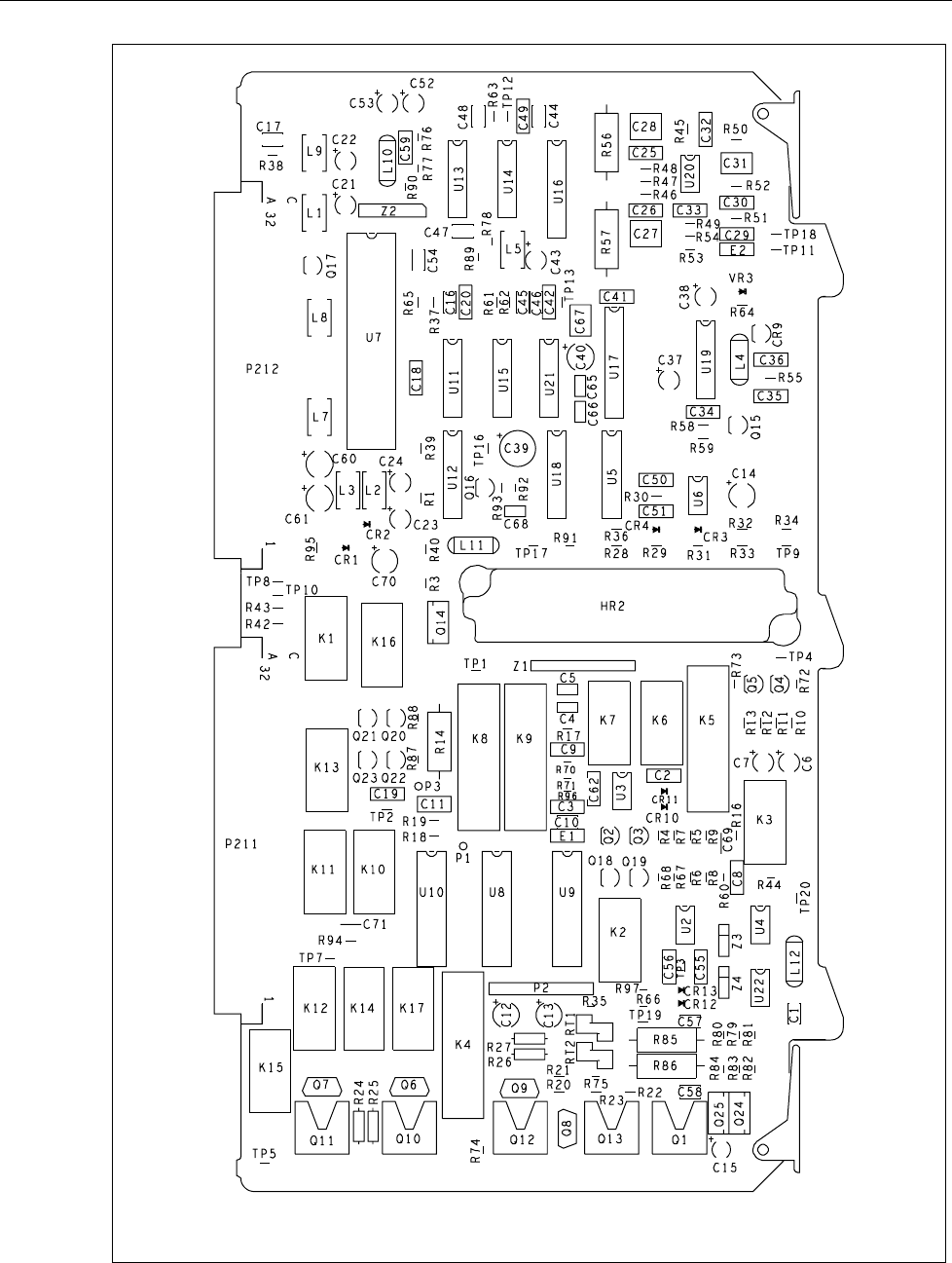
5700A/5720A Series II Calibrator
Service Manual
6-32
5700A-1621
57001621.EPS
Figure 6-10. A7 Current/HIgh-Res Oscillator PCA

List of Replaceable Parts
Service Centers
6
6-33
Table 6-9. A8 Switch Matrix PCA
Reference
Designator Description Fluke Stock
No Tot Qty Notes
C1,C3,C18 CAP,CER,470PF,+-10%,50V,C0G 733071 3
C2,C5 CAP,CER,33PF,+-5%,50V,C0G 714543 2
C4 CAP,CER,0.01UF,+80-20%,50V,Z5V 697284 1
C6-9,C12 C13,
C15,C16 C21,
C25-27
CAP,POLYES,0.22UF,+-5%,50V 747519
747519
747519
12
C10,C29 CAP,CER,100PF,+-20%,50V,C0G 721605 2
C14 CAP,CER,15PF,+-2%,100V,C0G 832287 1
C17 CAP,POLYES,1UF,+-10%,50V 733089 1
C20 CAP,CER,1000PF,+-20%,50V,X7R 697458 1
C22 CAP,TA,15UF,+-20%,20V 807610 1
C23 CAP,CER,22PF,+-2%,50V,C0G 714832 1
C30 CAP,CER,330PF,+-5%,50V,C0G 697441 1
C31 CAP,POLYES,0.1UF,+-10%,50V 649913 1
C32 CAPACITOR R05R,CAP,CER,220PF,+-20%,50V,C0G 740654 1
CR1,CR3,CR4,
CR7-9
*
*
DIODE,SI,BV=75V,IO=150MA,500MW 659516
659516
6
CR2,CR10 DIODE,SI,100 PIV,1.0 AMP 698555 2
CR5,CR6,CR12,
CR13
*
*
DIODE RL1N4007R05A,DIODE,SI,1KV,1A,DO-41 844647
844647
4
CR14,CR15 DIODE,SI,100 PIV,1 AMP 887203 2
H2 HYBRID ASSEMBLY, TESTED 813436 1
H5-8 RIVET,S-TUB,OVAL,AL,.087,.343 838458 4
K1,K3-6 K13,
K15-20, K22,
K24,K25
RELAY,ARMATURE,4 FORM C,5V,LATCH 715078
715078
715078
15
K2,K7-12,K14,
K21,K23 K26-33
RELAY,ARMATURE,2 FORM C,5V,LATCH 769307
769307
18
L1-4 CHOKE,6TURN 320911 4
MP2 MOLDED COVER, HYBRID, R-NET 775619 1
MP9,MP10 EJECTOR,PWB,NYLON 494724 2
MP18-21 SPACER,.156 RND,SOLUBLE,.062,.060 296319 8
P201,P202 CONN,DIN41612,TYPE C,RT ANG,64 PIN 807800 2
Q1 * TRANSISTOR,SI,BV=60V,65W,TO-22 386128 1
Q2 * TRANSISTOR,SI,NPN,SMALL SIGNAL 698225 1
Q4 * TRANSISTOR,SI,PNP,40V,0.35W,TO-92 698233 1
Q6,Q7,Q11 * TRANSISTOR,SI,N-DMOS PWR FET,T0-92 782565 3
Q9,Q10 * TRANSISTOR,SI,N-JFET,TO92 845073 2
Q12,Q13 * TRANSISTOR,SI,N-JFET,HI-VOLTAG 832147 2
R1 RES,MF,15.4K,+-1%,0.125W,100PPM 772038 1
R2 RES,MF,1.21K,+-1%,0.125W,100PPM 810507 1
R3,R4,R6 RES,CF,10K,+-5%,0.25W 697102 3
R5,R7,R10,R19,
R34
RES,MF,1K,+-1%,0.125W,100PPM 816595
816595
5
R8 RES,MF,12.7K,+-1%,0.125W,25PPM 817510 1
R9,R46,R47 RES,MF,10K,+-0.1%,0.125W,50PPM 733972 3
R11,R20,R35 RES,CF,560,+-5%,0.25W 810440 3
R12 RES,CF,1.5,+-5%,0.25W 732800 1
R13 RES,CF,330,+-5%,0.25W 830596 1
R14 RES,CF,4.7K,+-5%,0.25W 721571 1
R15-17,R21 RES,CF,100K,+-5%,0.25W 658963 4
R18,R33,R44 RES,MF,20K,+-0.1%,0.25W,25PPM 810564 3
R22 RES,CF,1K,+-5%,0.25W 780585 1
R23,R39,R40 RES,CF,100,+-5%,0.25W 810465 3
R24 1/4 WATT HERM. W.W. RESISTOR 864207 1
R25 RES,CF,6.2K,+-5%,0.25W 714337 1
R26 RES,CF,9.1K,+-5%,0.25W 706663 1

5700A/5720A Series II Calibrator
Service Manual
6-34
Table 6-9. A8 Switch Matrix PCA (cont)
Reference
Designator Description Fluke Stock
No Tot Qty Notes
R27,R28 RES,CF,620,+-5%,0.25W 810408 2
R29,R30 RES,MF,14.3,+-1%,0.125W,100PPM 831396 2
R32 RES,MF,10,+-1%,0.125W,100PPM 820399 1
R36,R37 RES,MF,4.99K,+-1%,0.125W,100PPM 721548 2
R38 RESISTOR A52R,RES,MF,46.4,+-1%,0.125W,100PPM 686995 1
R41,R42 RES,CF,20,+-5%,0.25W 810382 2
R43 RES,MF,150,+-1%,0.125W,100PPM 822171 1
T1 MV COMMON MODE CHOKE 802751 1
TP1-10 JUMPER,WIRE,NONINSUL,0.200CTR 816090 10
U1 * IC,CMOS,PROGRMBL PERIPHERAL INTERFACE 780650 1
U2 * IC,CMOS,BCD-DEC & BINRY-OCTALTAL DECODER 650689 1
U3 * IC,BPLR,FAHRENHEIT TEMPERTURE SENSOR 845156 1
U4 * IC,CMOS,8-1 LINE MUX/DEMUX ANALOG SW 836304 1
U5-13 * IC,BIMOS,8 CHNL HI-VOLT DRVR W/LATCH 782912 9
U15 * IC,COMPARATOR,DUAL,LO-PWR,8 PIN 478354 1
U17 * IC,OP AMP,GEN PURPOSE,COMPEMSATED 402750 1
U19 * IC,ARRAY,5 TRANS,5 ISO: 2-PNP,3-NPN 418954 1
U20 * IC,OP AMP,PRECISION,LOW NOISE 782920 1
U21 * IC,OP AMP,LO-OFFSET VOLTAGE,LO-NOISE 605980 1
VR1,VR2 * ZENER 1N754A A52R,ZENER,UNCOMP,6.8V,5%,20.0MA,0.4W 260695 2
VR3,VR4 * ZENER,UNCOMP,5.1V,5%,20.0MA,0.5W 853700 2
Z1 RNET,MF,HERM,SIP,5700 LO V DIVIDER 759647 1
Z2 * RNET,MF,POLY,SIP,8840 LO V DIVIDER 655811 1
Z3,Z4 RES,CERM,SIP,6 PIN,5 RES,330,+-2% 408302 2
Z5 RES,CERM,SIP,8 PIN,4 RES,10K,+-2% 513309 1
Z6 RES,CERM,SIP,6 PIN,5 RES,1K,+-2% 408310 1
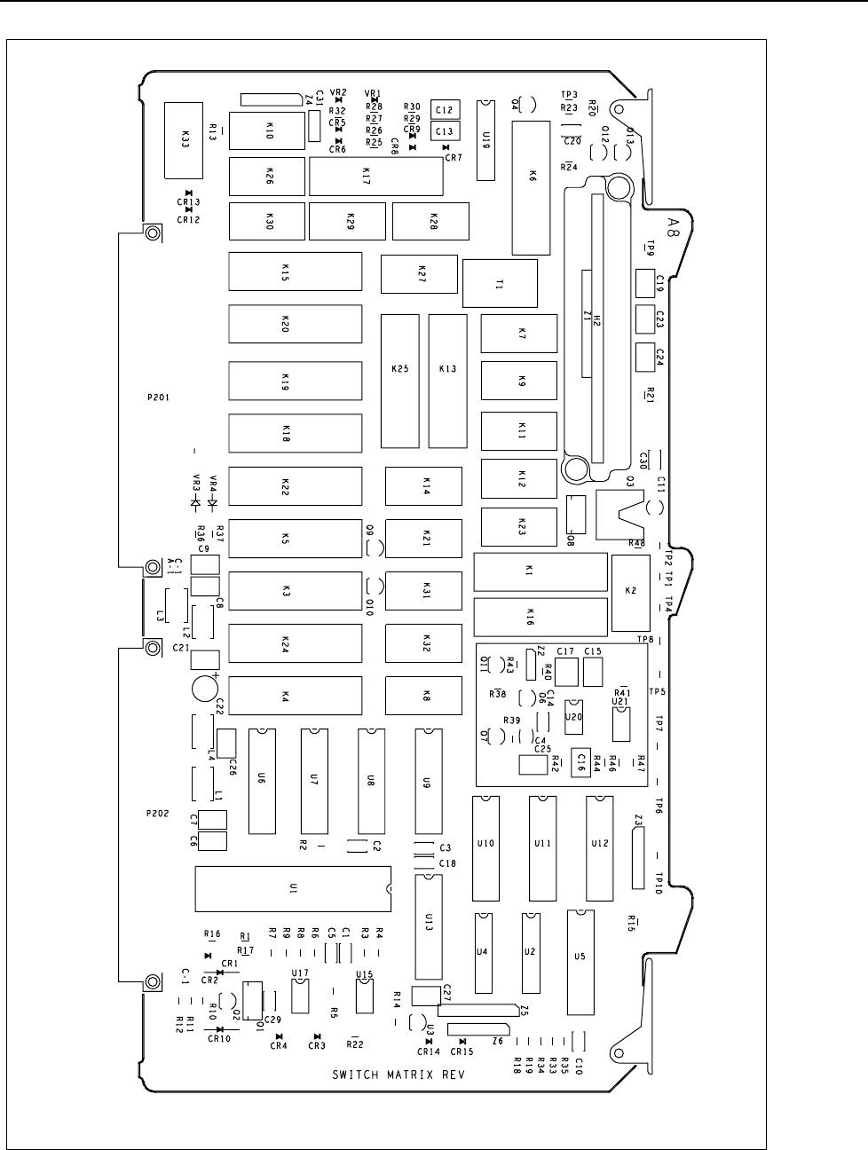
List of Replaceable Parts
Service Centers
6
6-35
5700A-1622
57001622.EPS
Figure 6-11. A8 Switch Matrix PCA

5700A/5720A Series II Calibrator
Service Manual
6-36
Table 6-10. A9 Ohms Cal PCA
Reference
Designator Description Fluke Stock
No Tot Qty Notes
C1,C28,C29 C55 CAP,POLYES,0.1UF,+-10%,50V 649913 4
C2,C3,C32,C35 CAP,CER,1000PF,+-20%,100V,X7R 816181 4
C4,C5,C8,C10,
C14,C15,C31,
C37-43 C45
CAP,POLYES,0.22UF,+-5%,50V 747519
747519
747519
15
C6 CAP,CER,470PF,+-10%,50V,C0G 733071 1
C7,C9,C22 C23 CAP,TA,2.2UF,+-10%,35V 697433 4
C12,C13 CAP,CER,220PF,+-20%,50V,C0G 740654 2
C16,C17 CAP,CER,22PF,+-5%,50V,C0G 714550 2
C18,C33 CAP,TA,4.7UF,+-20%,25V 807644 2
C19,C24,C25 CAP,TA,10UF,+-20%,35V 816512 3
C20,C52 CAP,CER,0.22UF,+80-20%,50V,Z5U 649939 2
C21 CAP,CER,2700PF,+-5%,50V,C0G 832303 1
C26,C27 CAP,CER,1800PF,+-5%,50V,C0G 832717 2
C30 CAP,POLYPR,0.1UF,+-10%,160V 446781 1
C34,C51 CAP,CER,33PF,+-5%,50V,C0G 714543 2
C36 CAP,TA,47UF,+-20%,10V 733246 1
C48 CAP,POLYPR,0.47UF,+-10%,160V 446807 1
C53,C54 CAP,POLYES,1UF,+-10%,50V 733089 2
CR1-10 * DIODE,SI,BV=75V,IO=150MA,500MW 659516 10
H1-4 RIVET,S-TUB,OVAL,AL,.087,.343 838458 4
H5 SCREW,PH,P,LOCK,STL,6-32,.250 152140 1
K1-5,K10 K11,
K13 K15-18,K20,
K22-27,K31
RELAY,ARMATURE,2 FORM C,5V,LATCH 769307
769307
769307
20
K6-9,K12 K14,
K19,K21 K28-30
RELAY,ARMATURE,4 FORM C,5V,LATCH 715078
715078
11
L2-8 CHOKE,6TURN 320911 7
M4 SHIELD, OHMS CAL 775312 1
MP1,MP2 EJECTOR,PWB,NYLON 494724 2
MP3 SLEEV,PVC,.500ID,CLEAR 113761 1
MP4 SHIELD, HIGH VOLTAGE CONTROL 761197 1
MP6-17 SPACER,.156 RND,SOLUBLE,.062,.060 296319 12
P311,P312 CONN,DIN41612,TYPE C,RT ANG,64 PIN 807800 2
Q1 * TRANSISTOR,SI,BV=60V,65W,TO-22 386128 1
Q2-4 * TRANSISTOR,SI,VMOS,PWR,TO-237,UV10KM 640516 3
Q5 * TRANSISTOR,SI,PNP,40V,0.35W,TO-92 698233 1
Q6 * TRANSISTOR,SI,NPN,SMALL SIGNAL 698225 1
R1-3,R80 RES,CF,10K,+-5%,0.25W 697102 4
R4,R8,R13,R32,
R35,R39 R45
RES,CF,1K,+-5%,0.25W 780585
780585
7
R9,R10,R43 R44 RES,CF,47,+-5%,0.25W 822189 4
R11 RESISTOR A52R,RES,MOX,330,+-5%,1W,200PPM 689604 1
R12,R23 RES,CF,100K,+-5%,0.25W 658963 2
R14,R15 RES,CF,24,+-5%,0.25W 817528 2
R16,R17 RES,MF,10K,+-0.1%,0.125W,100PPM 658955 2
R18 RES,MF,76K,+-0.1%,0.125W,50PPM 851332 1
R24,R31 RES,CF,22K,+-5%,0.25W 747535 2
R25 RESISTOR A52R,RES,MOX,150,+-5%,1W,200PPM 689612 1
R26,R46 RES,CF,100,+-5%,0.25W 810465 2
R27 RES,MF,10K,+-1%,0.125W,100PPM 658914 1
R29,R30 RES,CF,200,+-5%,0.25W 810390 2
R33 RES,CF,16K,+-5%,0.25W 714303 1
R41 RES. SET,1.0 OHM 0.04% 3PPM TC 824193 1
R42 RES. SET,1.9 OHM 0.04% 3PPM TC 824201 1
T1 TRANSFORMER, OHMS 2W COMP 802652 1
List of Replaceable Parts
Service Centers
6
6-37
Table 6-10. A9 Ohms Cal PCA (cont)
Reference
Designator Description Fluke Stock
No Tot Qty Notes
TP1,TP2,TP5-20 JUMPER,WIRE,NONINSUL,0.200CTR 816090 18
U1-3 * IC,OP AMP,LO-OFFSET VOLTAGE,LO-NOISE 605980 3
U4 * IC,OP AMP,PRECISION,LOW NOISE 782920 1
U5 * IC,OP AMP,GEN PURPOSE,COMPEMSATED 402750 1
U6 * IC,BIPOLAR,REG PULSE WIDTH MODULATOR 811935 1
U7 * IC,OP AMP,CHOPPER STABLIZED,LOW NOISE 810952 1
U8,U9 * IC,OP AMP,LO-NOISE,8 PIN DIP 495051 2
U10 * IC,OP AMP,DUAL,JFET INPUT,8 PIN 854059 1
U11 * IC,CMOS,PROGRMBL PERIPHERAL INTERFACE 780650 1
U12 * IC,CMOS,BCD-DEC & BINRY-OCTAL DECODER 650689 1
U13 * IC,CMOS,3-8 LINE DCDR W/ENABLE 773036 1
U14-20 * IC,BIMOS,8 CHNL HI-VOLT DRVR W/LATCH 782912 7
U21 * IC,CMOS,8-1 LINE MUX/DEMUX ANALOG SW 836304 1
U22 * IC,CMOS,HEX INVERTER,UNBUFFERED 741199 1
VR1,VR2 * ZENER 1N756A A52R,ZENER,UNCOMP,8.2V,5%,20.0MA,0.4W 386771 2
VR3 * ZENER,UNCOMP,3.3V,5%,20.0MA,0.4W 820423 1
Z1 * RNET,CERM,SIP,5700 LO V INST AMP 813659 1
Z2 * RNET,CERM,SIP,5700 LO V AMP GAIN 809368 1
Z3 RES,CERM,SIP,10 PIN,5 RES,10K,+-2% 529990 1
Z4 RES,CERM,SIP,6 PIN,5 RES,1K,+-2% 408310 1
Z5 RNET,MF,HERM,SIP,5700 LO V DIVIDER 915889 1
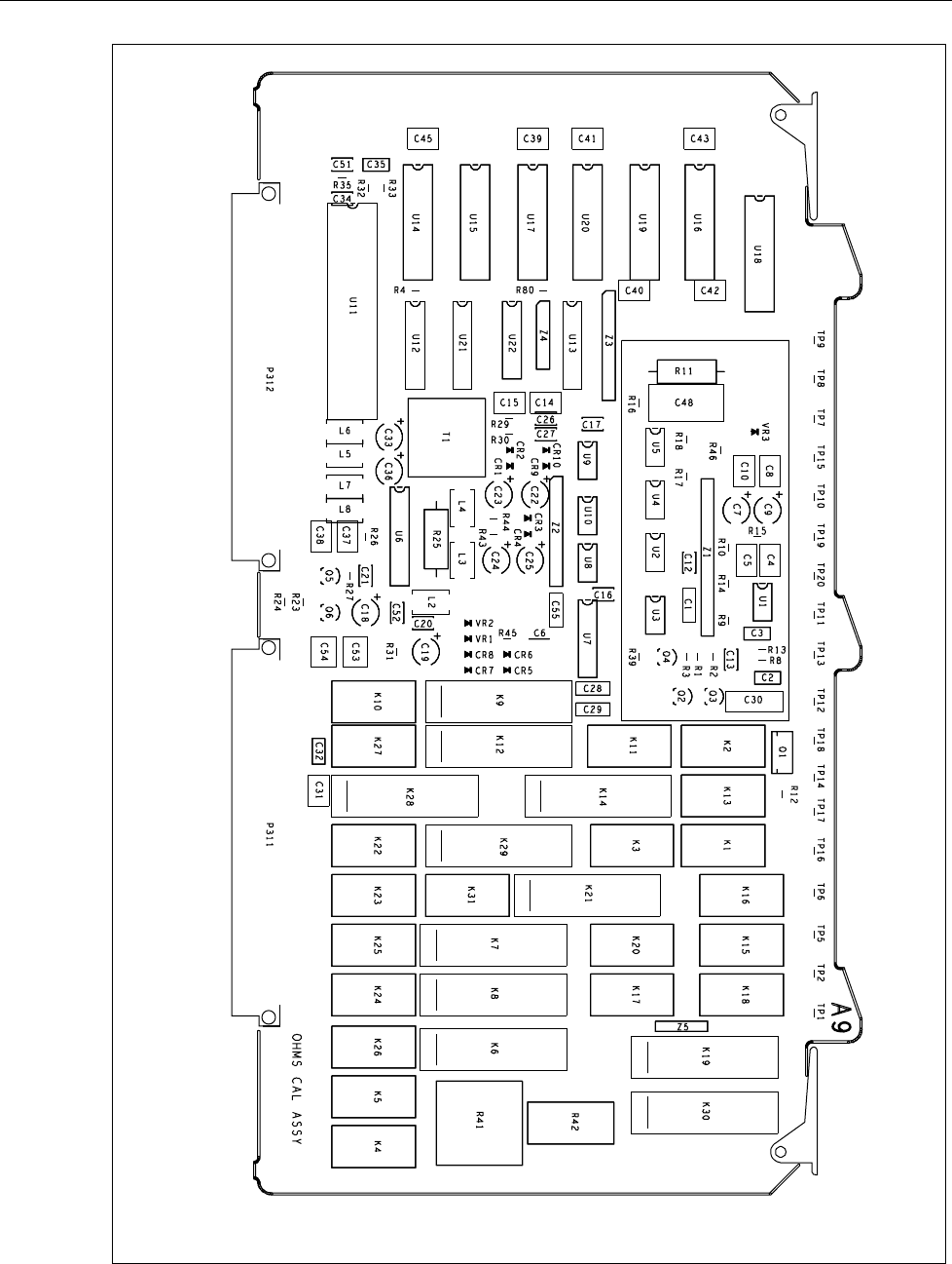
5700A/5720A Series II Calibrator
Service Manual
6-38
5700A-1631
57001631.EPS
Figure 6-12. A9 Ohms Cal PCA

List of Replaceable Parts
Service Centers
6
6-39
Table 6-11. A10 Ohms Main PCA
Reference
Designator Description Fluke Stock
No Tot Qty Notes
C1,C2,C7 C10-
13,C16
CAP,POLYES,0.22UF,+-5%,50V 747519
747519
8
C3,C4 CAP,TA,10UF,+-20%,35V 816512 2
C6 CAP,TA,4.7UF,+-20%,25V 807644 1
H3-6 RIVET,S-TUB,OVAL,AL,.087,.343 838458 4
H7,H8 SCREW,PH,P,LOCK,STL,6-32,.250 152140 2
K1-4,K7,K9,K10,
K13-17,K28-30,
K33-37
RELAY,ARMATURE,2 FORM C,5V,LATCH 769307
769307
769307
20
K5 RELAY,REED,1 FORM A,5VDC 806950 1
K6,K8,K11,K12 RELAY,REED,1 FORM A,4.5VDC 544031 4
K18-27,K31 K32,
K39
RELAY,ARMATURE,4 FORM C,5V,LATCH 715078
715078
13
K38 RELAY,ARMATURE,2 FORM C,5V 733063 1
L4,L5 CHOKE,6TURN 320911 2
MP1,MP2 SPACER,SWAGE,.250 RND,BR,6-32,.875 266486 2
MP3,MP4 EJECTOR,PWB,NYLON 494724 2
MP6 FOOT,RUBBER,ADHES,BLK,.50 SQ,.12 THK 543488 1
MP7 * OHMS, MAIN, HEAT SHIELD 872325 1
P301,P302 CONN,DIN41612,TYPE C,RT ANG,64 PIN 807800 2
R1 R-NET, THIN FILM, TESTED, FRIT 103306 1
R2,R3 RES,CF,270,+-5%,0.25W 810424 2
R5 RES,CF,100,+-5%,0.25W 810465 1
R6 RES,MF,110K,+-1%,0.125W,100PPM 234708 1
TP1-5 JUMPER,WIRE,NONINSUL,0.200CTR 816090 5
U1 * IC,OP AMP,JFET INPUT,LOW NOISE 807933 1
U2,U3 U5-8,
U11-13
*
*
IC,BIMOS,8 CHNL HI-VOLT DRVR W/LATCH 782912
782912
9
U9 * IC,CMOS,BCD-DEC & BINRY-OCTAL DECODER 650689 1
U10 * IC,CMOS,3-8 LINE DCDR W/ENABLE 773036 1
VR1 * ZENER,UNCOMP,3.3V,5%,20.0MA,0.4W 820423 1
Z1 * RNET,MF,HERM,SIP,5700 RESISTANCE REF 798330 1
Z2 * RNET,MF,HERM,SIP,5700 RESISTANCE REF 759753 1
Z3 * RNET,MF,HERM,SIP,5700 RESISTANCE REF 759803 1
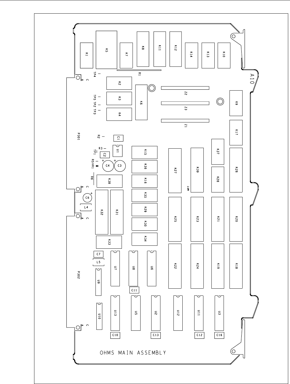
5700A/5720A Series II Calibrator
Service Manual
6-40
5700A-1630
57001630.EPS
Figure 6-13. A10 Ohms Main PCA

List of Replaceable Parts
Service Centers
6
6-41
Table 6-12. A11 DAC PCA
Reference
Designator Description Fluke Stock
No Tot
Qty Notes
A1 DAC FILTER SIP PCA 761395 1
A2 * DAC BUFFERED REFERENCE SIP PCA 764639 1
C1,C2,C4-8,C10,
C11,C13-18, C21,
C23-26, C41,C42
C46-49,C53-56,
C58,C62,C64,
C65,C76,C77,
C81,C86-88, C91,
C92,C96-98,C100
C104-109
CAP,CER,0.22UF,+80-20%,50V,Y5V 740597
740597
740597
740597
740597
740597
740597
740597
740597
52
C3 CAP,CER,3300PF,+-10%,25V,X7R,0805 602870 1
C9,C12 CAP,AL,10UF,+-20%,63V,SOLV PROOF 816843 2
C19,C20 CAP,TA,2.2UF,+-10%,35V 697433 2
C27 CAP,CER,15PF,+-20%,50V,C0G 697524 1
C29 CAP,CER,220PF,+-2%,100V,C0G 816728 1
C30,C31 CAP,TA,1.5UF,+-20%,50V,6032 929302 2
C32 CAP,CER,0.1UF,+-10%,25V,X7R,1206 747287 1
C40,C80 CAP,CER,47PF,+-10%,50V,C0G,12006 747352 2
C43 CAP,CER,0.01UF,+-10%,50V,X7R,1206 747261 1
C44,C60,C63 C94,
C102
CAP,CER,1000PF,+-10%,50V,C0G,1206 747378
747378
5
C45,C89,C95 CAP,POLYPR,0.1UF,+-10%,160V 446781 3
C52,C101,C103 CAP,CER,33PF,+-10%,50V,C0G,1206 769240 3
C57,C85 CAP,CER,22PF,+-5%,50V,C0G 714550 2
C59,C67 CAP,CER,100PF,+-10%,50V,C0G,1206 740571 2
C78 CAP,POLYES,0.47UF,+-10%,50V 697409 1
C79 CAP,CER,10PF,+-10%,100V,C0G,1206 806943 1
C84 CAP,POLYPR,0.022UF,+-10%,160V 494948 1
C90 CAP,POLYPR,0.033UF,+-10%,63V 721050 1
C93 CAP,CER,330PF,+-5%,50V,C0G 697441 1
C110,C111 CAP,POLYES,0.22UF,+-10%,50V 706028 2
CR1,CR3-6,CR8,
CR12,CR13
*
*
DIODE,SI,BV=75V,IO=150MA,500MW 659516
659516
8
CR2 * DIODE,SI,N-JFET,CURRENT REG,IF 741512 1
CR7 * DIODE,SI,N-JFET,CURRENT REG,IF 334839 1
CR9,CR10 * DIODE,SI,BV=75V,IO=250MA,SOT-2 830489 2
CR14 * DIODE,SI,N-JFET,CURRENT REG,IF 852116 1
H1 SCREW,PH,P,LOCK,SS,6-32,.500 320051 1
H9-12 RIVET,S-TUB,OVAL,AL,.087,.343 838458 4
H21 SCREW,PH,P,LOCK,STL,4-40,.187 129882 1 2
H26 NUT,HEX,STL,4-40 184044 1 2
H28 TERM,RING 5/64 & .144,SOLDR 101055 1 2
H32 SHIELD, DAC, FRONT 797761 1
HR5 * REFERENCE HYBRID ASSY 893334 1
HR6 * DC AMP HYBRID ASSY 761411 1
K1,K2,K4 RELAY,ARMATURE,4 FORM C,5V,LATCH 715078 3
K3,K5,K8 RELAY,ARMATURE,2 FORM C,5V,LATCH 769307 3
L1-7,L10 CHOKE,6TURN 320911 8
M2 SHIELD, DAC-ADC AMP 775353 1
M3 SHIELD, DAC, REAR 761429 1
MP1 MOLDED COVER, HYBRID, R-NET 775619 1
MP2,MP3 SPACER,SWAGE,.250 RND,BR,6-32,.875 266486 2
MP5,MP6 EJECTOR,PWB,NYLON 494724 2
MP7-9 HEAT DIS,PWB MT,.75X.50X.50,TO-220 816587 3 2
MP10 HEAT DIS,VERT,.75X.52X.50,TO-220 811760 1 2
MP11 SHIELD, DAC, FRONT, SMALL 797720 1

5700A/5720A Series II Calibrator
Service Manual
6-42
Table 6-12. A11 DAC PCA (cont)
Reference
Designator Description Fluke Stock
No Tot
Qty Notes
MP31 MOLDED COVER, REF. HYBRID 797746 1
P401,P402 CONN,DIN41612,TYPE C,RT ANG,64 PIN 807800 2
Q1 * TRANSISTOR,SI,BV=60V,65W,TO-220 386128 1
Q2,Q3 * TRANSISTOR,SI,BV=40V,40W,TO-220 369660 2 1
Q4-7,Q11,Q22,
Q25,Q26
*
*
TRANSISTOR,SI,N-DMOS PWR FET,T0-92 782565
782565
8
Q8 * TRANSISTOR,SI,PNP,SMALL SIG,SE 380394 1
Q9 * TRANSISTOR,SI,BV=60V,65W,TO-220 386128 1
Q10,Q19,Q56 * TRANSISTOR,SI,NPN,SMALL SIGNAL 698225 3
Q12,Q13,Q16,
Q17,Q23,Q24
*
*
TRANSISTOR,SI,N-JFET,HI-VOLTAG 832147
832147
6
Q14,Q15,Q18,
Q20,Q21,Q52, Q53
*
*
*
TRANSISTOR,SI,N-CHAN,TO-92,SWI 832139
832139
832139
7
Q30,Q32 * TRANSISTOR,SI,N-JFET,SOT-23 844584 2
Q31,Q33,Q35 * TRANSISTOR,SI,NPN,SMALL SIGNAL 806463 3
Q34 * TRANSISTOR,SI,PNP,SMALL SIGNAL 838516 1
Q57 * TRANSISTOR,SI,PNP,40V,0.35W,TO-92 698233 1
R1,R28,R33,R39,
R44,R83 R84
*
*
RES,CERM,4.7K,+-5%,.125W,200PPM 740522
740522
7
R2 RES,CF,3K,+-5%,0.25W 810366 1
R3 RES,CF,2K,+-5%,0.25W 441469 1
R6 * RES,CERM,910,+-5%,.125W,200PPM 769257 1
R7 * RES,CERM,620,+-5%,.125W,200PPM 745984 1
R9,R107,R108 * RES,CERM,1.8K,+-5%,.125W,200PPM 746453 3
R10 RES,MF,2.49K,+-1%,0.125W,100PPM 810523 1
R12 * RES,CERM,200,+-5%,.125W,200PPM 746339 1
R13 * RES,CERM,22,+-5%,.125W,200PPM 746230 1
R14 RES,MF,61.9M,+-1%,0.25W,150PPM 851741 1
R15 RES,MF,1.21K,+-1%,0.125W,100PPM 810507 1
R16 * RES,CERM,750,+-5%,.125W,200PPM 746404 1
R19-21,R29,R31,
R41,R48
*
*
RES,CERM,10K,+-5%,.125W,200PPM 746610
746610
10
R22 RES,CF,20K,+-5%,0.25W 697110 1
R23 RESISTOR SMR,RES,CERM,6.8,+-5%,.125W,300PPM,1206 811802 1
R24 * RES,CERM,2.49K,+-1%,.125W,100PPM 806448 1
R25 * RES,CERM,51.1,+-1%,.125W,100PPM 806422 1
R26,R27,R70,R89,
R90
RES,MF,20K,+-0.1%,0.25W,25PPM 810564
810564
5
R30,R50,R85 * RES,CERM,510,+-5%,.125W,200PPM 746388 3
R32 * RES,CERM,10,+-5%,.125W,200PPM 746214 1
R36,R77,R78,
R103,R105
*
*
RES,CERM,1.2K,+-5%,.125W,200PPM 746412
746412
5
R37,R106,R110 * RES,CERM,12,+-5%,.125W,200PPM 845458 3
R38,R49 * RES,CERM,270,+-5%,.125W,200PPM 746354 2
R40 * RES,CERM,100K,+-5%,.125W,200PPM 740548 1
R43,R52,R109 * RES,CERM,3K,+-5%,.125W,200PPM 746511 3
R45 * RES,CERM,2.7K,+-5%,.125W,200PPM 746503 1
R46 * RES,CERM,360,+-5%,.125W,200PPM 783290 1
R47,R60,R62,R66,
R75,R76
*
*
RES,CERM,100,+-5%,.125W,200PPM 746297
746297
6
R51 * RES,CERM,150,+-1%,.125W,100PPM 772780 1
R53,R71 * RES,CERM,5.1K,+-5%,.125W,200PPM 746560 2
R58,R59,R64,
R73,R124-127
*
*
RES,CERM,56K,+-5%,.125W,200PPM 746701
746701
8
R61 RES,CF,1.5K,+-5%,0.25W 810432 1
R63,R65,R95,
R96,R99
*
*
RES,CERM,1K,+-5%,.125W,200PPM 745992
745992
5
R128 RESISTOR SMR,RES,CERM,200K,+-1%,0.1W,100PPM,0805 928882 1
1. Assembly 665448 consists of 369660 and 816587
2. Assembly 665510 consists of part numbers 811760, 129882, 101055, 184044, and 690587

List of Replaceable Parts
Service Centers
6
6-43
Table 6-12. A11 DAC PCA (cont)
Reference
Designator Description Fluke
Stock No Tot Qty Notes
R68 RES,MF,40K,+-0.1%,0.125W,100PPM 821702 1
R69 RES,MF,18.12K,+-0.1%,0.125W,50PPM 734020 1
R72 RES,CF,200,+-5%,0.25W 810390 1
R74 * RES,CERM,470K,+-5%,.125W,200PPM 746792 1
R79-81 * RES,CERM,100K,+-1%,.125W,100PPM 769802 3
R82,R115,R116 * RES,CERM,10K,+-5%,.125W,200PPM 746610 0
R86,R87,R100 * RES,CERM,330,+-5%,.125W,200PPM 746370 3
R88 RES,MF,50K,+-0.1%,0.25W,25PPM 810580 1
R91 RES,MF,4.12K,+-1%,0.125W,100PPM 820381 1
R92,R94 * RES,CERM,2K,+-5%,.125W,200PPM 746461 2
R93 * RES,CERM,8.06K,+-1%,.125W,100PM 806356 1
R97,R98,R114 * RES,CERM,22K,+-5%,.125W,200PPM 746651 3
R104 * RES,CERM,15K,+-5%,.125W,200PPM 746628 1
R111 RES,CF,33K,+-5%,0.25W 733667 1
R112,R113 RES,CF,10K,+-5%,0.25W 697102 2
R117-119,R123 * RES,CERM,7.5K,+-5%,.125W,200PPM 746586 4
T1 PULSE TRANSFORMER 802892 1
TP1,TP3 TP8-10,
TP12
JUMPER,WIRE,NONINSUL,0.200CTR 816090
816090
6
U1 * IC,OP AMP,DUAL,LO OFFST VOLT,L0-DRIFT 851704 1
U2,U20 * IC,OP AMP,DUAL,PRECISION,8-PIN 783696 2
U5 * IC,OP AMP,OPA548,+-4 TO +-30V,10MV OFFSET,1MHZ,HI V-
I,TO-220-7
690578 1 1
U6 * IC,CMOS,PROGRMBL INTERVAL TIME 806612 1
U7 * IC,COMPARATOR,HI-SPEED,PRECISIION 822197 1
U8 * IC,CMOS,OCTL INV LINE DRVR,SOIC 782938 1
U9 * IC,CMOS,QUAD 2 INPUT OR GATE,SOIC 783712 1
U10 * IC,COMPARATOR,HI-SPEED,14 PIN 647115 1
U11 * IC,OP AMP,SINGLE,LOW NOISE FAST,SOIC 783720 1
U12,U37 * ISOLATOR,OPTO,LED TO TRANSISTOR 454330 2
U13 * ISOLATOR, 20 MHZ OPTOCOUPLER 742817 1
U14 * IC,CMOS,DUAL D F/F,+EDG TRG,SOIC 782995 1
U15 * IC,CMOS,DUAL MONOSTB MULTIVBRTR,SOIC 806620 1
U19 * IC,OP AMP,DUAL,PRECISION MATCH 782375 1
U22 * IC,OP AMP,JFET INPUT,22V SUPPLY,DIP 832584 1
U23 * IC,DMOS,QUAD ANALOG SWITCH,SOIC 928291 1
U24 * IC,OP AMP,PRECISION,JFET INPUT 808097 1
U25 IC,CMOS,RR A/D CONVERTER 715680 1
U26 * IC,OP AMP,DUAL,LO-NOISE,8 PIN 707976 1
U27,U28 * IC,OP AMP,DUAL,JFET IN,HIGH SPEED 855069 2
U29 * IC,OP AMP,JFET INPUT,8 PIN DIP 472779 1
U31 * IC,CMOS,PROGRAMBL PERIPH INTRF 806604 1
U32 * IC,CMOS,3-8 LINE DCDR W ENABLE 783019 1
U33,U34 * IC,BIMOS,8 CHNL HI-VOLT DRVR W/LATCH 782912 2
U35,U36 * IC,COMPARATOR,QUAD,14 PIN,SOIC 741561 2
U38 * IC,OP AMP,JFET INPUT,8 PIN DIP 472779 1
VR1,VR17,VR21,
VR31,VR32
* ZENER 5250 SMR,ZENER,UNCOMP,20V,5%,6.2MA,0.2W,SOT-23 642469
642469
5
VR2,VR8,VR24 * ZENER 5240 SMR,ZENER,UNCOMP,10V,5%,20MA,0.2W,SOT-23 783704 3
VR3 * ZENER 5246 SMR,ZENER,UNCOMP,16V,5%,7.8MA,0.2W,SOT-23 642485 1
VR4 * ZENER 5248 SMR,ZENER,UNCOMP,18V,5%,7MA,0.2W,SOT-23 876433 1
VR5,VR19,VR20,
VR35,VR36
*
*
ZENER,UNCOMP,3.3V,5%,20.0MA,0.4W 820423
820423
5
VR6,VR30 * ZENER,UNCOMP,12.0V,10%,10.5MA,0.4W 741074 2
VR7,VR16 * ZENER 5251 SMR,ZENER,UNCOMP,22V,5%,5.6MA,0.2W,SOT-23 831230 2
VR10-VR12 * ZENER,UNCOMP,10V,5%,20MA,0.2W,SOT-23 783704 3
1. Assembly 665510 uses 5 parts: 811760, 129882, 101055, 184044, and 690578

5700A/5720A Series II Calibrator
Service Manual
6-44
Table 6-12. A11 DAC PCA (cont)
Reference
Designator
Description Fluke
Stock
No
Tot
Qty Notes
VR13 * ZENER 5243 SMR,ZENER,UNCOMP,13V,5%,9.5MA,0.2W,SOT-23 642477 1
VR18,VR22 * ZENER 5245 SMR,ZENER,UNCOMP,15V,5%,8.5MA,0.2W,SOT-23 837187 2
VR25 * ZENER,UNCOMP,3.3V,10%,20.0MA,0.4W 309799 1
VR26 * ZENER,UNCOMP,3.3V,5%,20MA,0.2W 807008 1
VR27 * ZENER,UNCOMP,7.5V,5%,20MA,0.2W 837138 1
VR28 * ZENER,UNCOMP,8.2V,5%,20MA,0.2W 837146 1
VR29 * ZENER,COMP,6.4V,2%,2PPM,1MA 419036 1
VR33,VR34 * ZENER 5236 SMR,ZENER,UNCOMP,7.5V,5%,20MA,0.2W,SOT-23 837138 2
X1 SOCKET,IC,40 PIN,DUAL WIPE,RETENTION 756668 1
Z2 * RNET,MF,POLY,SIP,5700 LO V DIVIDER 890244 1
Z4 RES,CERM,SIP,10 PIN,5 RES,56K,+-2% 529131 1
Z5 RES,CERM,SIP,6 PIN,5 RES,510,+-2% 459974 1
Z8 * RNET,MF,HERM,SIP,5700 LO V INST AMP 809418 1
Z10 RNET,MF,HERM,SIP,5700 A TO D CONV 833830 1
Z12 RES,CERM,SIP,6 PIN,5 RES,10K,+-2% 500876 1
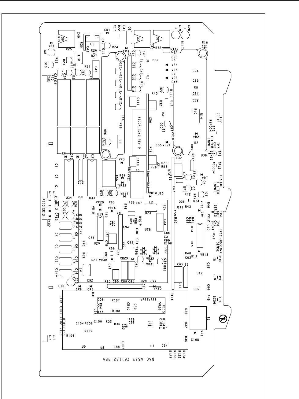
List of Replaceable Parts
Service Centers
6
6-45
5700A-1640
57001640.EPS
Figure 6-14. A11 DAC PCA
5700A/5720A Series II Calibrator
Service Manual
6-46
Table 6-13. A11A1 DAC Filter SIP PCA
Reference
Designator Description Fluke Stock
No Tot Qty Notes
C1-6 CAP,POLYES,0.33UF,+-20%,50V 853903 6
C10,C11 CAP,POLYPR,1UF,+-5%,50V,HERMETIC 783811 2
C12,C13 CAP,CER,0.22UF,+80-20%,50V,Y5V,1206 740597 2
C14 CAP,CER,100PF,+-10%,50V,C0G,1206 740571 1
P21,P22 HEADER,2 ROW,.100CTR,RT ANG,6 PIN 912217 2
R1,R2 * RES,CERM,11K,+-5%,.125W,250PPM 769752 2
R3,R5 * RES,CERM,18K,+-5%,.125W,200PPM 746636 2
R4 * RES,CERM,22K,+-5%,.125W,200PPM 746651 1
U1 * IC,OP AMP,ULTRA-LOW-NOISE,SOIC 783001 1
U2 * IC,OP AMP,PRECISION,LOW NOISE 782920 1
VR1 * ZENER,UNCOMP,15.0V,5%,8.5MA,0.4W 266601 1
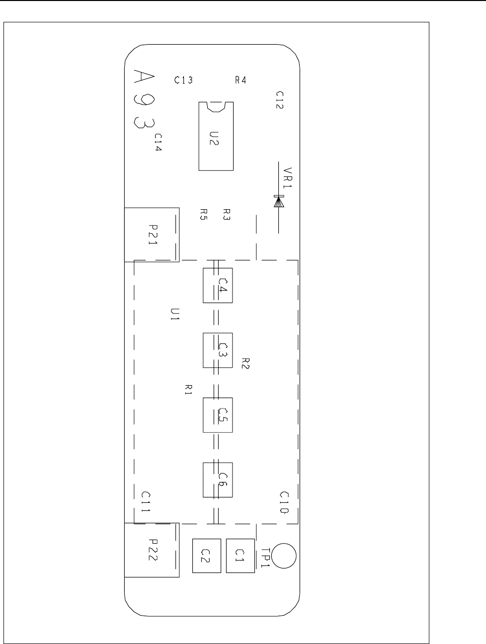
List of Replaceable Parts
Service Centers
6
6-47
5700A-1643
57001643.EPS
Figure 6-15. A11A1 DAC Filter SIP PCA
5700A/5720A Series II Calibrator
Service Manual
6-48
Table 6-14. A11A2 DAC Buffered Reference SIP PCA
Reference
Designator Description Fluke Stock
No Tot Qty Notes
C1,C5 CAP,CER,10PF,+-10%,100V,C0G,1206 806943 2
C2,C3 CAP,CER,0.22UF,+80-20%,50V,Y5V 740597 2
C4,C6 CAP,CER,1000PF,+-10%,50V,C0G,1206 747378 2
P11 HEADER,2 ROW,.100CTR,RT ANG,10 PIN 658112 1
P12 HEADER,2 ROW,.100CTR,RT ANG,8 PIN 424200 1
Q1-15 * TRANSISTOR,SI,N-JFET,HI-VOLTAG 832147 15
R1,R6-8 * RES,CERM,1K,+-5%,.125W,200PPM 745992 4
R5 * RES,CERM,10,+-5%,.125W,200PPM 746214 1
R9 * RES,CERM,100K,+-1%,.125W,100PPM 769802 1
U1 * IC,OP AMP,DUAL,PRECISION,8-PIN 783696 1
VR1 * ZENER,UNCOMP,22.0V,5%,5.6MA,0.4W 181073 1
Z1 RES,CERM,SIP,10 PIN,5 RES,56K,+-2% 529131 1
Z2 RES,CERM,SIP,6 PIN,5 RES,51K,+-2% 514042 1
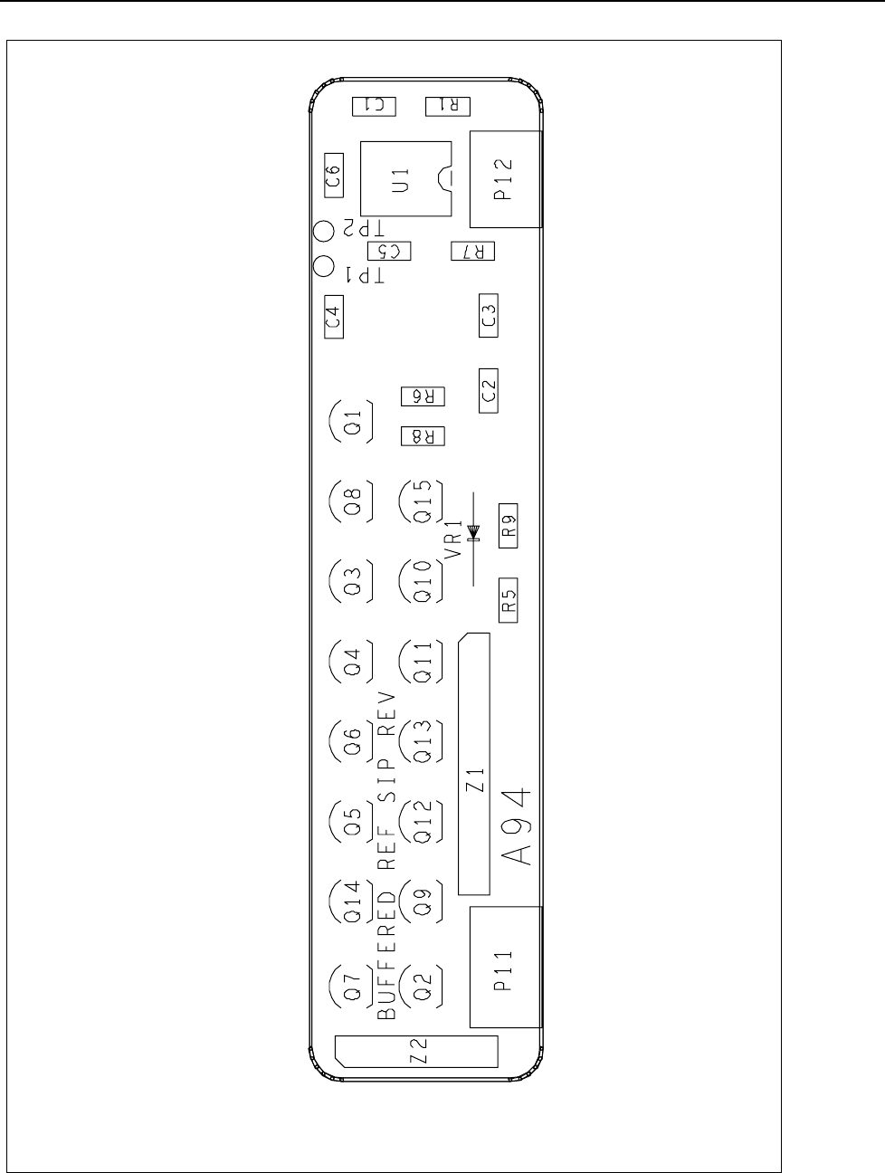
List of Replaceable Parts
Service Centers
6
6-49
5700A-1644
57001644.EPS
Figure 6-16. A11A2 DAC Buffered Reference SIP PCA

5700A/5720A Series II Calibrator
Service Manual
6-50
Table 6-15. A12 Oscillator Control PCA
Reference
Designator Description Fluke Stock
No Tot Qty Notes
C1-4,C12 C14,
C16,C18 C48
CAP,TA,4.7UF,+-20%,25V 807644
807644
9
C8,C10 CAP,AL,2.2UF,+-20%,50V 769687 2
C21 CAP,CER,10PF,+-10%,3000V,C0G 817049 1
C22,C25 CAP,TA,330UF,+-20%,3V 385963 2
C23,C24 C36-
38,C44-47 C49,
C50,C56 C57,
C61,C64 C65,
C67,C68 C70-
72,C76-81
CAP,POLYES,0.22UF,+-5%,50V 747519
747519
747519
747519
747519
747519
27
C26,C29,C30,
C42, C60
CAP,POLYES,0.47UF,+-10%,50V 697409
697409
5
C27,C28,C31,
C43, C63
CAP,POLYES,0.047UF,+-10%,50V 820548
820548
5
C33,C58,C59 CAP,CER,120PF,+-5%,50V,C0G 721142 3
C34,C35,C86, C87 CAP,AL,47UF,+-20%,50V,SOLV PROOF 822403
822403
4
C39,C53 CAP,CER,330PF,+-5%,50V,C0G 697441 2
C40,C41 CAP,TA,10UF,+-20%,25V 714774 2
C51,C52,C66 CAP,CER,82PF,+-2%,50V,C0G 714857 3
C54 CAP,CER,3.3PF,+0.25PF,100V,C0J 816678 1
C55 CAP,CER,6.8PF,+-0.25PF,50V,C0G 715243 1
C62 CAP,POLYES,1UF,+-10%,50V 733089 1
C69,C90,C91 CAP,POLYES,0.01UF,+-10%,50V 715037 3
C74 CAP,CER,3300PF,+-5%,50V,C0G 830612 1
C75,C88 CAP,CER,33PF,+-5%,50V,C0G 714543 2
C82,C85 CAP,POLYES,0.022UF,+-10%,50V 715268 2
C83 CAP,CER,150PF,+-10%,50V,X7R 682377 1
C84 CAP,POLYPR,0.47UF,+-10%,160V 446807 1
CR1-3 * DIODE,SI,BV=75V,IO=150MA,500MW 659516 3
CR4,CR5 * DIODE,SI,SCHOTTKY BARRIER,SMALL SIGNL 408815 2
CR6-8 * DIODE,SI,BV=75V,IO=150MA,500MW 203323 3
CR12-15 * DIODE,SI,BV=70V,500MW 851910 4
H4-7 RIVET,S-TUB,OVAL,AL,.087,.343 838458 4
H13 SCREW,PH,P,LOCK,STL,6-32,.250 152140 1
HS1 HEAT DIS,RAD,.54X1.25X.35,TO-8 808204 1
K1 RELAY,ARMATURE,4 FORM C,5V,LATCH 715078 1
K2-9 RELAY,ARMATURE,2 FORM C,5V,LATCH 769307 8
L1-4 CHOKE,6TURN 320911 4
MP8,MP9 EJECTOR,PWB,NYLON 494724 2
M12 OSCILLATOR THERMAL COVER 797696 1
MP10 SHIELD, HIGH VOLTAGE CONTROL 761197 1
MP14 SPACER,.375 RND,SOLUBLE,.10THK 837823 1
P501,P502 CONN,DIN41612,TYPE C,RT ANG,64 PIN 807800 2
Q1 * TRANSISTOR,SI,100V,10W,TO-202 943803 1
Q2 * TRANSISTOR,SI,BV=100V,10W,TO-202 943790 1
Q3 * TRANSITOR,SI,PNP,SMALL SIG,TO-92 851977 1
Q4 * TRANSISTOR,SI,NPN SMALL SIGNAL 853478 1
Q5,Q9,Q11 * TRANSISTOR,SI,N-JFET,TO-92 832162 3
Q6,Q7,Q12 Q18,
Q20
*
*
TRANSISTOR,SI,N-CHAN,TO-92,SWI 832139
832139
5
Q8,Q13 * TRANSITOR,SI,N-JFET,UHF/VHF US 851972 2
Q10 * TRANSISTOR,SI,P-MOS,ZENER PROTECTED 306142 1
Q14 * TRANSISTOR,SI,NMOS,1W,4 PIN DIVIDER 853692 1
Q19 * TRANSISTOR,SI,N-DMOS FET,TO-72 394122 1
R1,R2,R55 RES,CF,30K,+-5%,0.25W 368753 3

List of Replaceable Parts
Service Centers
6
6-51
Table 6-15. A12 Oscillator Control PCA (cont)
Reference
Designator Description Fluke
Stock
No
Tot Qty Notes
R3 RES,MF,143K,+-1%,0.125W,100PPM 291336 1
R4,R12 RES,CF,3K,+-5%,0.25W 441527 2
R5,R13,R25 R48,
R52,R53 R68, R69
RES,CF,1K,+-5%,0.25W 343426
343426
343426
8
R6 RES,CF,750,+-5%,0.25W 810374 1
R7 RES,CF,200,+-5%,0.25W 810390 1
R8-10 RES,MF,113K,+-1%,0.125W,100PPM 291302 3
R11 RES,CF,20K,+-5%,0.25W 697110 1
R14 RES,CF,22K,+-5%,0.25W 348870 1
R15 RES,CF,5.1K,+-5%,0.25W 368712 1
R16 RES,CF,15,+-5%,0.25W 348755 1
R17,R39 RES,CF,510,+-5%,0.25W 441600 2
R18 RES,CF,47,+-5%,0.25W 822189 1
R19 RES,CF,10,+-5%,0.25W 807669 1
R20 RES,MF,301K,+-1%,0.125W,25PPM 379156 1
R21 RES,CF,2K,+-5%,0.25W 441469 1
R22,R24,R29, R66 RES,CF,100K,+-5%,0.25W 348920
348920
4
R23,R30,R33 RES,CF,100K,+-5%,0.25W 658963 3
R26 RES,MF,316K,+-1%,0.125W,100PPM 289496 1
R27,R28,R70 RES,CF,1K,+-5%,0.25W 780585 3
R31,R37,R45 RES,MF,866,+-0.1%,0.125W,50PPM 838441 3
R32 RES,CF,120,+-5%,0.25W 442293 1
R34 RES,MF,3.61K,+-0.25%,0.25W,100PPM 832394 1
R35,R36,R40, R41 RES,MF,649K,+-1%,0.125W,100PPM 375972
375972
4
R38,R42 RES,MF,357K,+-1%,0.125W,25PPM 312793 2
R43,R63-65 RES,CF,20K,+-5%,0.25W 441477 4
R44 RES,CF,2.2K,+-5%,0.25W 343400 1
R46 RES,CF,12K,+-5%,0.25W 348847 1
R47 RES,CF,560,+-5%,0.25W 385948 1
R49,R54,R56 RES,CF,10K,+-5%,0.25W 348839 3
R50 RES,CF,47,+-5%,0.25W 441592 1
R55 RESISTOR A52R,RES,CF,30K,+-5%,0.25W 368753 1
R57 RES,MF,60.4K,+-1%,0.125W,100PPM 291419 1
R58 RES,MF,1K,+-1%,0.125W,100PPM 168229 1
R59,R60 RES,MF,4.99K,+-1%,0.125W,100PPM 721548 2
R62 RES,CF,4.7K,+-5%,0.25W 348821 1
R67 RES,MF,562K,+-1%,0.125W,100PPM 757815 1
TP1-8 JUMPER,WIRE,NONINSUL,0.200CTR 816090 8
U1,U3 * IC,OP AMP,50MHZ,CURRENT FEEDBACK AMP 836262 2
U2,U7 * IC,OP AMP,HI-SLEW RATE,8 PIN DIP 386268 2
U5,U26 * IC,OP AMP,LO-OFFSET VOLTAGE,LO-NOISE 605980 2
U8 * IC,ANALOG SWITCH,DG211,+-15V,175 OHMS,QUAD BILATERAL,DIP16 586735 1
U9 * IC,OP AMP,DUAL,JFET INPUT,8 PIN 495192 1
U10 * IC,CMOS,14BIT DAC,12BIT ACC,CUR OUT 773101 1
U11,U30,U31 * IC,OP AMP,PRECISION,LOW NOISE 782920 3
U12 * IC,OP AMP,DUAL,PRECISION MATCH 782375 1
U13 * IC,OP AMP,JFET INPUT,WIDE BAND 808105 1
U14,U16 OP AMP LT1220CST ON 12 PIN ADAPTER BOARD 1577442 2 1
U15 * IC,OP AMP,QUAD JFET INPUT,14 PIN 659748 1
U17 * IC,ARRAY,5 TRANS,NPN,3 ISO,2 DEFF CON 248906 1
U18 * IC,CMOS,8-1 LINE MUX/DEMUX ANALOG SW 836304 1
U20 * IC,CMOS,PROGRMBL PERIPHERAL INTERFACE 780650 1
U19 CMOS DG444 ,IC,CMOS,QUAD BILATERAL SWITCH 910708 1
U21,U22 * IC,COMPARATOR,QUAD,14 PIN DIP 387233 2
U23,U24 * IC,BIMOS,8 CHNL HI-VOLT DRVR W/LATCH 782912 2

5700A/5720A Series II Calibrator
Service Manual
6-52
Table 6-15. A12 Oscillator Control PCA (cont)
Reference
Designator Description Fluke Stock
No Tot Qty Notes
U25 * IC,VOLT REG,FIXED,+5 VOLTS,1.5 AMPS 428847 1
VR1,VR2 * ZENER,UNCOMP,10.0V,5%,12.5MA,0.4W 246611 2
VR3 * ZENER,UNCOMP,5.1V,5%,20.0MA,0.4W 159798 1
VR4 * ZENER,UNCOMP,6.8V,2%,175.0MA,5.0W 325845 1
VR5,VR6 * ZENER,UNCOMP,6.8V,5%,37.0MA,1.0W 454595 2
VR7,VR8 * ZENER,UNCOMP,5.1V,5%,20.0MA,0.5W 853700 2
Z1 * RNET,CERM,SIP,5700 LO V AMP GAIN 760686 1
Z2,Z4 * RNET,MF,POLY,SIP,8840 LO V DIVIDER 655811 2
Z3 RNET,MF,HERM,SIP,5700 LO V DIVIDER 760645 1
Z5 RES,CERM,DIP,14 PIN,7 RES,10K,+-2% 601911 1
Z6 RES,CERM,SIP,8 PIN,7 RES,1K,+-2% 414557 1
Z7,Z8 * RNET,CERM,SIP,5700 LO V DIVIDER 785105 2
Z9 RES,CERM,DIP,16 PIN,8 RES,5.1K,+-5% 544130 1
Z10 RES,CERM,SIP,8 PIN,4 RES,4.7K,+-2% 573881 1
1. U14, U16, part number 1577442 are assemblies
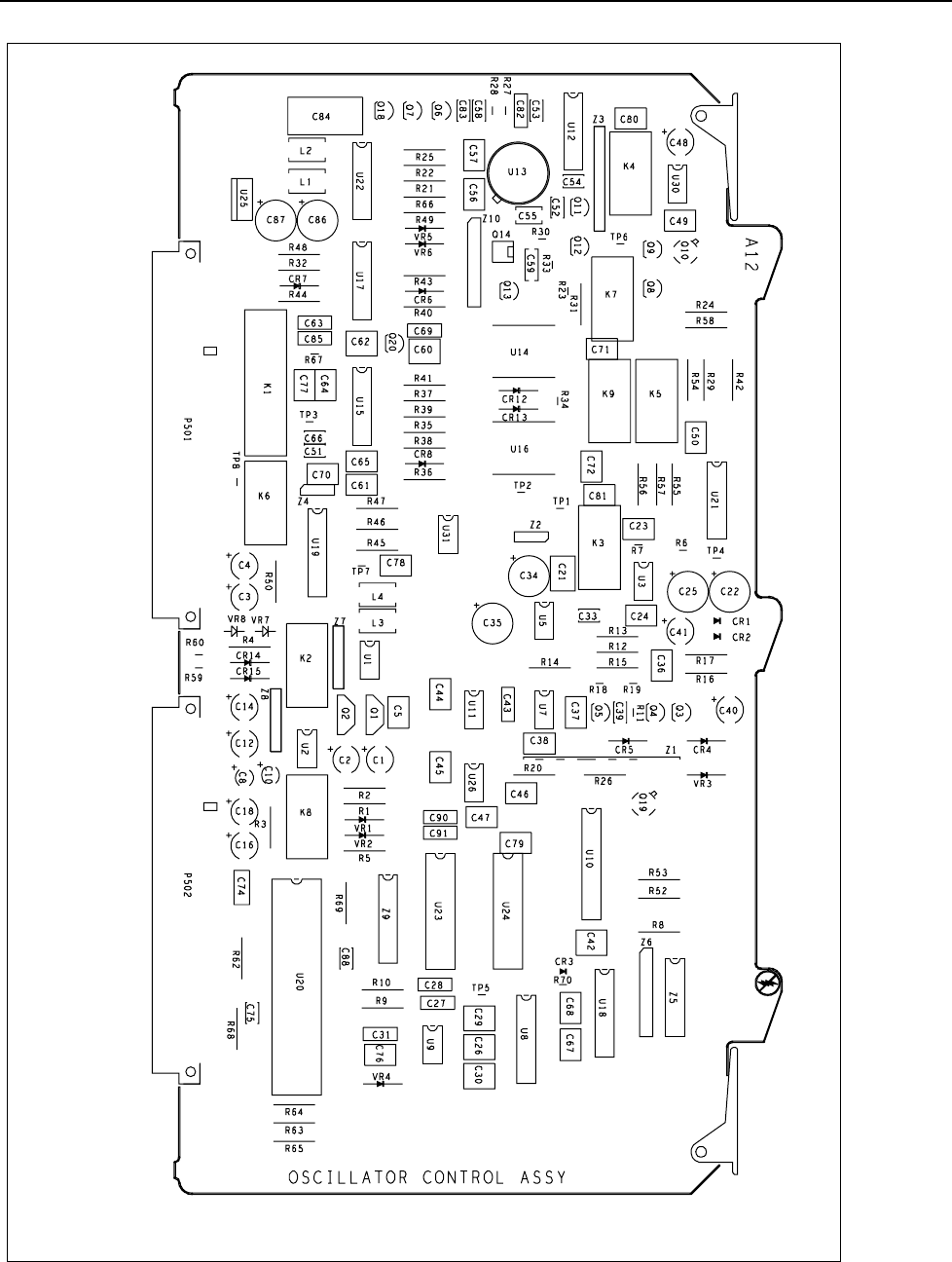
List of Replaceable Parts
Service Centers
6
6-53
5700A-1650
57001650.EPS
Figure 6-17. A12 Oscillator Control PCA

5700A/5720A Series II Calibrator
Service Manual
6-54
Table 6-16. A13 Oscillator Output PCA
Reference
Designator Description Fluke Stock
No Tot Qty Notes
C2-4,C16, C20,
C23 C26-28,C32,
C33,C46,C47,
C51,C52,C54,
C55,C68-71 C88-
92,C102-104,
C110,C111,
C113,C114
CAP,POLYES,0.22UF,+-5%,50V 747519
747519
747519
747519
747519
747519
747519
747519
33
C5,C14,C30 CAP,CER,15PF,+-20%,50V,C0G 697524 3
C6,C15,C31 CAP,CER,82PF,+-2%,50V,C0G 714857 3
C7,C8 CAP,CER,0.01UF,+-10%,100V,X7R 557587 2
C17,C29 CAP,CER,2.7PF,+-0.25PF,50V,C0G 773044 2
C19,C34,C85 CAP,CER,56PF,+-2%,50V,C0G 714378 3
C21,C37 CAP,MICA,560PF,+-1%,300V 494609 2
C22,C38 CAP,POLYCA,6150PF,+-1%,50V 800466 2
C24,C40 CAP,POLYCA,0.0621UF,+-1%,50V 800482 2
C25,C41 CAP,POLYCA,0.622UF,+-1%,50V 800474 2
C44,C123 CAP,CER,10PF,+-20%,50V,C0G 721589 2
C45 CAP,POLYPR,0.033UF,+-10%,63V 721050 1
C48,C84 CAP,AL,10UF,+-20%,16V,NP,SOLV 697177 2
C49 CAP,AL,470UF,+-20%,10V,SOLV PROOF 822387 1
C56-59 CAP,TA,22UF,+-20%,10V 658971 4
C60,C61,C108,
C109
CAP,TA,4.7UF,+-20%,25V 807644
807644
4
C62 CAP,POLYES,0.47UF,+-10%,50V 697409 1
C75 CAP,CER,120PF,+-5%,50V,C0G 721142 1
C76,C77,C124,
C125
CAP,CER,1000PF,+-20%,50V,X7R 697458
697458
4
C78,C79 CAP,POLYES,0.01UF,+-10%,50V 715037 2
C80,C81 CAP,POLYES,0.1UF,+-10%,50V 649913 2
C82,C83 CAP,POLYES,1UF,+-10%,50V 733089 2
C93-99,C106,
C107
CAP,TA,10UF,+-20%,25V 714774
714774
9
C100,C101,C118 CAP,AL,2.2UF,+-20%,50V 769687 3
C105 CAP,CER,3300PF,+-5%,50V,C0G 830612 1
C112 CAP,CER,4.7PF,+-0.25PF,50V,C0G 721837 1
C115 CAP,CER,6800PF,+-5%,100V,C0G 816710 1
C116,C117 CAP,AL,10UF,+-20%,63V,SOLV PROOF 816843 2
C119,C120 CAP,CER,33PF,+-5%,50V,C0G 714543 2
C122 CAP,CER,27PF,+-2%,100V,C0G 816652 1
C126,C127 CAP,CER,39PF,+-2%,50V,C0G 714840 2
CR1-11,CR22,
CR23
*
*
DIODE,SI,BV=75V,IO=150MA,500MW 659516
659516
13
CR13-20 * DIODE,SI,N-JFET,CURRENT REG,IF 852116 8
H4-7 RIVET,S-TUB,OVAL,AL,.087,.343 838458 4
H9-12 SCREW,PH,P,LOCK,STL,6-32,.250 152140 4
HS1-3 HEAT DIS,RAD,.54X1.25X.35,TO-8 808204 3
HS4-7 HEAT DIS,CLIP,.80X.85X.30,CASE 800136 4
HS9,HS10 HEAT DIS,VERT,.83,.50,.395,TO-5 800144 2
K1 RELAY,ARMATURE,4 FORM C,5V,LATCH 715078 1
K2-4 RELAY,ARMATURE,2 FORM C,5V,LATCH 769307 3
L1-5,L13,L14 CHOKE,6TURN 320911 7
L6-12 CORE,TOROID,FERRITE,.047X.138X.118 321182 7
L15 TRANSFORMER, PULSE 660589 1
MP2,MP3 EJECTOR,PWB,NYLON 494724 2
MP4-6 INSUL PT,TRANSISTOR MOUNT,DAP,TO-5 152207 4
MP8 AIR DUCT, OSCILLATOR 939509 1

List of Replaceable Parts
Service Centers
6
6-55
Table 6-16. A13 Oscillator Output PCA (cont)
Reference
Designator Description Fluke Stock
No Tot Qty Notes
MP13-15 SPACER,.375 RND,SOLUBLE,.10THK 837823 3
P511,P512 CONN,DIN41612,TYPE C,RT ANG,64 PIN 807800 2
Q6 * TRANSISTOR,SI,N-JFET,TO-92 832162 1
Q7 * TRANSISTOR,SI,N-DMOS FET,TO-72 394122 1
Q8 * TRANSISTOR,SI,NPN,SM SIGNAL,HI 272930 1
Q9 * TRANSISTOR,SI,NPN,SMALL SIGNAL 698225 1
Q10,Q11 * TRANSISTOR,SI,100V,10W,TO-202 943803 2
Q13 * TRANSISTOR,SI,BV=115V,3W,TO-126 601242 1
Q14 * TRANSISTOR,SI,PNP,70V,400MA,TO-39 866769 1
Q15 * TRANSISTOR,SI,PNP,40V,0.35W,TO-92 698233 1
Q16,Q17 * TRANSISTOR,SI,BV=100V,10W,TO-202 943790 2
R1,R6,R43 R60,
R65
RES,MF,2K,+-1%,0.125W,100PPM 816629
816629
5
R2,R40,R64,R67,
R69,R72, R108-
110
RES,CF,1K,+-5%,0.25W 780585
780585
780585
9
R7,R9,R11,R18 RES,CF,200,+-5%,0.25W 810390 4
R12,R13,R83 RES,MF,4.99K,+-1%,0.125W,100PPM 721548 3
R19,R37,R50 RES,CF,10K,+-5%,0.25W 697102 5
R25 RES,CF,39K,+-5%,0.25W 912621 1
R28 RES,MF,1K,+-1%,0.125W,100PPM 816595 1
R29,R62,R68 RES,MF,10K,+-1%,0.125W,100PPM 658914 3
R32 RES,CF,20K,+-5%,0.25W 697110 1
R33,R38,R51,
R78
RES,CF,16K,+-5%,0.25W 714303
714303
4
R35,R36,R47,
R52,R53,R59,
R63,R74,R75,
R80-82,R107,
RES,CF,4.7K,+-5%,0.25W 721571
721571
721571
721571
13
R39,R54,R76 RES,CF,12K,+-5%,0.25W 757799 3
R41 RES,CF,100K,+-5%,0.25W 658963 1
R42 RES,MF,10.5K,+-1%,0.125W,100PPM 816611 1
R48 RES,CF,51K+-5%,0.25W 747550 1
R49 RES,CF,270,+-5%,0.25W 810424 1
R55,R77 RES,CF,24K,+-5%,0.25W 697599 2
R56 RES,MF,34.8K,+-0.1%,0.125W,50PPM 772582 1
R57 RES,CF,43K,+-5%,0.25W 821777 1
R58 RES,CF,47K,+-5%,0.25W 721787 1
R61,R66 RES,MF,7.87K,+-1%,0.125W,100PPM 810549 2
R71,R73 RES,CF,3K,+-5%,0.25W 810366 2
R84,R85 RES,CF,33K,+-5%,0.25W 733667 2
R87,R94 RES,CF,100,+-5%,0.25W 810465 2
R88 RES,CF,4.7,+-5%,0.25W 816637 1
R89,R90,R9, R98 RES,CF,10,+-5%,0.25W 807669 4
R91,R99 RES,CF,2.7,+-5%,0.25W 442061 2
R92,R93,R95, R96 RES,CF,3.9,+-5%,0.25W 810473
810473
4
R100,R101 RES,MF,30.1K,+-1%,0.125W,100PPM 772061 2
R111,R112 RES,CF,620,+-5%,0.25W 810408 2
S1 SWITCH,SLIDE,SPDT 477984 1
TP1-10 JUMPER,WIRE,NONINSUL,0.200CTR 816090 10
U2 * IC,VOLT REG,FIXED,-12 VOLTS,1.5 AMPS 381665 1
U3,U6,U9 * IC,OP AMP,JFET INPUT,WIDE BAND 808105 3
U5,U7 * RES NET HYBRID, TESTED 793885 2
U8,U29 * IC,OP AMP,HI-SLEW RATE,8 PIN DIP 386268 2
U10 * IC,MULTIPLIER/DIV,4 QUAD,10 MH,DIP 904714 1
5700A/5720A Series II Calibrator
Service Manual
6-56
Table 6-16. A13 Oscillator Output PCA (cont)
Reference
Designator Description Fluke Stock
No Tot Qty Notes
U11 * RES NET HYBRID, TESTED 793885 1
U12,U32,U33 * IC,CMOS,OCTL D F/F W/3-STATE,+EDG TRG 585364 3
U15,U16,U19 * IC,BPLR,FOUR-QUADRANT MULT,16 PIN DIP 343335 3
U17,U27 * IC,CMOS,DUAL 4-1 LINE MUX/DMUX ANL SW 429886 2
U18 * IC,OP AMP,JFET INPUT,8 PIN DIP 472779 1
U20 * IC,COMPARATOR,DUAL,LO-PWR,8 PIN 478354 1
U21 * IC,FTTL,QUAD 2 INPUT NAND GATE 654640 1
U22 * IC,FTTL,DUAL JK F/F,-EDG TRIG 781211 1
U23 * IC,COMPARATOR,DUAL,HI-SPEED,14 DIP 647123 1
U24 * IC,BIMOS,8 CHNL HI-VOLT DRVR W/LATCH 782912 1
U25 * IC,CMOS,8-1 LINE MUX/DEMUX ANALOG SW 836304 1
U26 * IC,CMOS,PROGRMBL PERIPHERAL INTERFACE 780650 1
U28 * IC,CMOS,DUAL 8 BIT DAC,CURRENT 722272 1
U31 * IC,OP AMP,DUAL,JFET INPUT,8 PIN 495192 1
VR3,VR4 * ZENER,UNCOMP,9.1V,5%,20MA,0.5W 853788 2
VR7 * ZENER,UNCOMP,8.2V,5%,20MA,0.4W 810309 1
Z1 RES,CERM,SIP,6 PIN,5 RES,39K,+-2% 831065 1
Z2 RES,CERM,DIP,14 PIN,7 RES,10K,+-2% 601911 1
Z3 RES,CERM,SIP,8 PIN,7 RES,1K,+-2% 414557 1
Z4,Z5 RES,CERM,SIP,8 PIN,4 RES,10K,+-2% 513309 2
Z6 RES,CERM,SIP,6 PIN,5 RES,3.6K,+-2% 478818 1
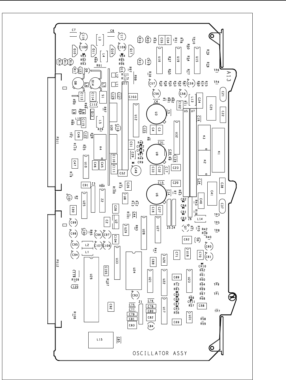
List of Replaceable Parts
Service Centers
6
6-57
5700A-1651
57001651.EPS
Figure 6-18. A13 Oscillator Output PCA

5700A/5720A Series II Calibrator
Service Manual
6-58
Table 6-17. A13A1 Oscillator Wideband SMD PCA
Reference
Designator Description Fluke Stock
No Tot Qty Notes
C1,C3,C4,C6-8,
C12,C13
CAP,CER,0.22UF,+80-20%,50V,Y5V 740597
740597
8
C2 CAP,CER,100PF,+-10%,50V,C0G,1206 740571 1
C5 CAP,CER,10PF,+-10%,100V,C0G,1206 806943 1
C9 CAP,CER,470PF,+-10%,50V,C0G,1206 747360 1
C10 CAP,CER,1000PF,+-10%,50V,C0G,1206 747378 1
C11 CAP,CER,0.01UF,+-10%,50V,X7R,1206 747261 1
CR4-6,CR9,C10 * DIODE,SI,BV=70V,IO=50MA,DUAL,SOT-23 742320 5
P1,P2 HEADER,2 ROW,.100CTR,RT ANG,1206 806935 2
Q1 * TRANSISTOR,SI,N-JFET,SOT-23 844584 1
Q2,Q4,Q5 * TRANSISTOR,SI,NPN,SMALL SIGNAL 845438 4
Q3 * TRANSISTOR,SI,PNP,SMALL SIGNAL 742684 1
Q6,Q8 * TRANSISTOR,SI,PNP,SMALL SIGNAL 838516 2
Q9 * TRANSISTOR,SI,NPN,SMALL SIGNAL 742676 1
R1,R9 * RES,CERM,2K,+-5%,.125W,200PPM 746461 2
R2 * RES,CERM,2.7K,+-5%,.125W,200PPM 746503 1
R3,R22 * RES,CERM,330,+-5%,.125W,200PPM 746370 2
R4,R26 * RES,CERM,510,+-5%,.125W,200PPM 746388 2
R5 * RES,CERM,5.1K,+-5%,.125W,200PPM 746560 1
R6,R23,R31 * RES,CERM,3.9K,+-5%,.125W,200PPM 746545 3
R7,R16,R18,R19,
R21 R27-29
*
*
RES,CERM,47,+-5%,.125W,200PPM 746263
746263
8
R8 * RES,CERM,100K,+-5%,.125W,200PPM 740548 1
R10 * RES,CERM,56,+-5%,.125W,200PPM 807727 1
R11,R17 * RES,CERM,150,+-1%,.125W,100PPM 772780 2
R12 * RES,CERM,27,+-5%,.125W,200PPM 807735 1
R13 * RES,CERM,100,+-5%,.125W,200PPM 746297 1
R14 * RES,CERM,750,+-5%,.125W,200PPM 746404 1
R15 * RES,CERM,15K,+-5%,.125W,200PPM 746628 1
R20 * RES,CERM,390,+-5%,.125W,200PPM 740498 1
R24 * RES,CERM,910,+-5%,.125W,200PPM 769257 1
R25 * RES,CERM,1.8K,+-5%,.125W,200PPM 746453 1 1
R30 RES,VAR,CERM,1K,+-10%,0.5W 912360 1
U1 * IC,OP AMP,ULTRA-LOW-NOISE,SOIC 783001 1
U2 * IC,OP AMP,SINGLE,LOW NOISE FAST,SOIC 783720 1
VR1,VR5-7 * ZENER,UNCOMP,6.2V,5%,20MA,0.2W 782441 4
VR2 * ZENER,UNCOMP,22V,5%,5.6MA,0.2W 831230 1
VR3,VR4 * ZENER,UNCOMP,3.3V,5%,20MA,0.2W 807008 2
1. R25 is selected at test as one of the following: 1.8k (746453), 2K (746461), or 2.2K.
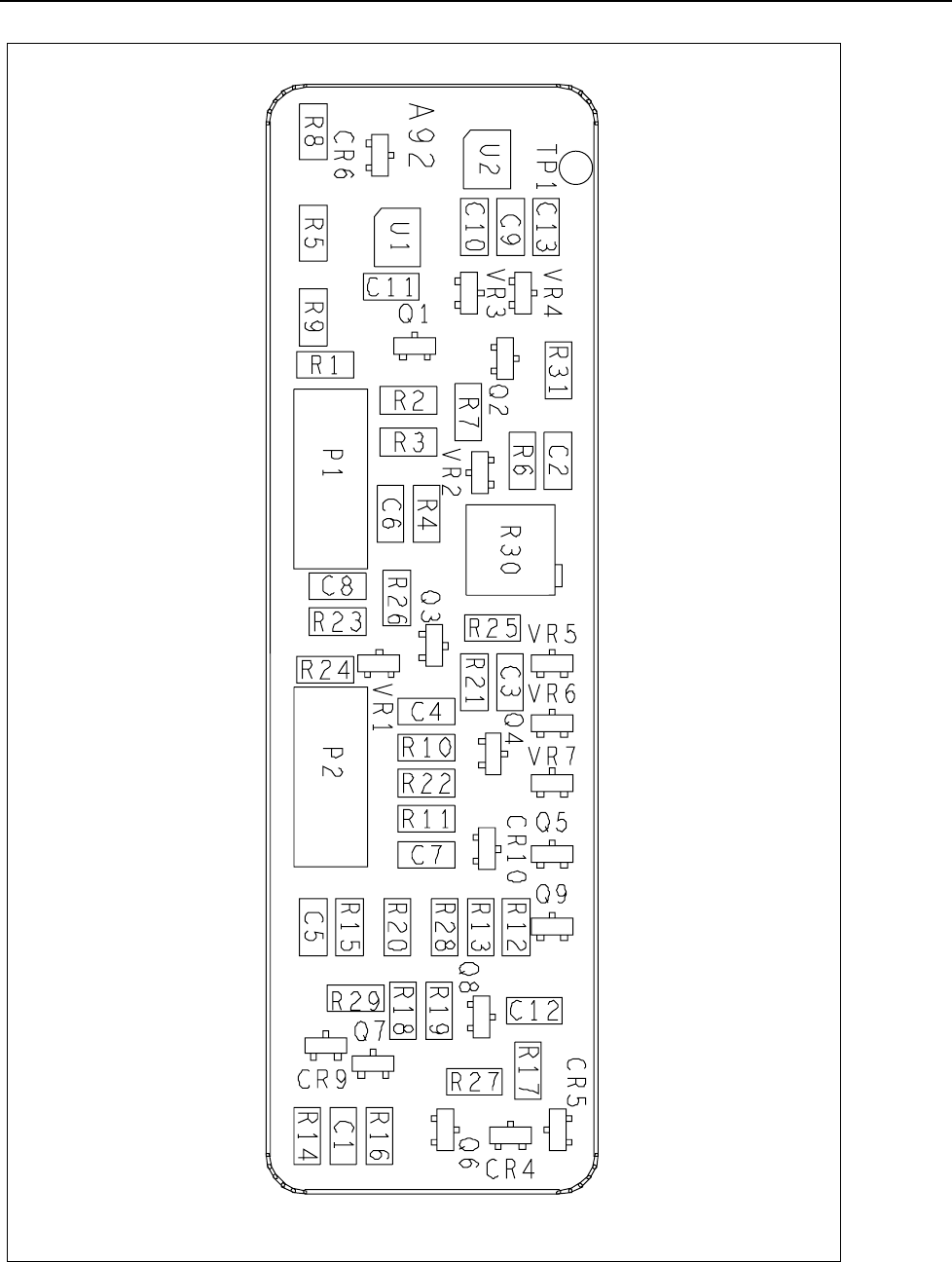
List of Replaceable Parts
Service Centers
6
6-59
5700A-1652
57001652.EPS
Figure 6-19. A13A1 Oscillator Wideband SMD PCA

5700A/5720A Series II Calibrator
Service Manual
6-60
Table 6-18. A14 High Voltage Control PCA
Reference
Designator Description Fluke Stock
No Tot Qty Notes
C1 CAP,POLYES,0.72UF,+-20%,1300V 853929 1
C2 CAP,POLYES,0.1UF,+-20%,1400V 821512 1
C3,C4 CAP,AL,470UF,+-20%,16V,SOLV PROOF 772855 2
C5 CAP,POLYES,1UF,+-10%,50V 733089 1
C6,C7 CAP,TA,10UF,+-20%,35V 816512 2
C8,C9 CAP,AL,10UF,+-20%,63V,SOLV PROOF 816843 2
C10,C20,C24-32 CAP,POLYES,0.1UF,+-10%,50V 649913 11
C11-13 CAP,TA,22UF,+-20%,10V 658971 3
C14 CAP,CER,330PF,+-5%,50V,C0G 697441 1
C15 CAP,CER,120PF,+-5%,50V,C0G 721142 1
C17 CAP,POLYES,2200PF,+-10%,50V 832683 1
C18 CAP,TA,1UF,+-20%,35V 697417 1
C21,C22 CAP,CER,33PF,+-5%,50V,C0G 714543 2
C23 CAP,CER,1000PF,+-20%,50V,X7R 697458 1
C33 CAP,CER,27PF,+-2%,100V,C0G 816652 1
CR1-4 * DIODE,SI,HIGH VOLTAGE,PIV=2K,4OMA 851956 4
CR5 DIODE,SI,RECT,BRIDGE,BV=50V,IO=3A 586115 1
CR6-12 * DIODE,SI,BV=75V,IO=150MA,500MW 659516 7
H4-7 RIVET,S-TUB,OVAL,AL,.087,.343 838458 4
H8,H9,H11 SCREW,PH,P,LOCK,STL,6-32,.250 152140 3
J1 CONN,MATE-N-LOK,HEADER,14 PIN 845318 1
K1,K2,K4 K8,
K10,K11,K14
RELAY,ARMATURE,2 FORM C,5V 733063
733063
7
K3,K5,K6 K9,
K12,K013 K15,
K16
RELAY,ARMATURE,1 FORM A/1 FORM 831545
831545
831545
8
K7 RELAY,ARMATURE,2 FORM C,5V,LATCH 769307 1
L1 CHOKE,6TURN 320911 1
MP1,MP2 EJECTOR,PWB,NYLON 494724 2
MP3 SHIELD, HIGH VOLTAGE CONTROL 761197 1
MP5 CABLE ACCESS,TIE,5.50L,.10W,1.25 DIA 530360 1
MP8 HEAT DIS,PRESS ON,TO-5 418384 1
MP10-13 WASHER,FLAT,STL,.149,.375,.031 110270 4
P611,P612 CONN,DIN41612,TYPE C,RT ANG,64 PIN 807800 2
Q2 * TRANSISTOR,SI,NPN,SMALL SIGNAL 698225 1
Q3,Q4 * TRANSISTOR,SI,P-JFET,TO-92 852111 2
R1,R2 RES,CC,47,+-5%,0.5W 644259 2
R3-5 RES,CC,200K,+-5%,1W 686774 3
R6,R8 RES,MF,23.2,+-1%,0.5W,100PPM 200790 2
R7 RES,CF,22K,+-5%,0.25W 747535 1
R9,R12,R64 RES,CF,1.5M,+-5%,0.25W 649962 3
R10,R11 RES,CF,1.5M,+-5%,0.25W 649962 2
R13 RES,CF,9.1K,+-5%,0.25W 706663 1
R14,R15 RES,CF,620,+-5%,0.25W 810408 2
R17,R46,R55 RES,CF,100K,+-5%,0.25W 658963 3
R18 RES,CF,1K,+-5%,0.25W 780585 1
R19 RES,MF,162K,+-1%,0.125W,100PPM 817569 1
R20 RES,MF,412K,+-1%,0.125W,50PPM 714287 1
R21,R24,R33,
R34,R47,R56,
R68,R69
RES,CF,10K,+-5%,0.25W 697102
697102
697102
8
R22 RES,CC,3K,+-5%,0.5W 641115 1
R23 RES,CF,200K,+-5%,0.25W 681841 1
R25 RES,CF,750K,+-5%,0.25W 747543 1
R26,R44,R45 RES,MF,100K,+-1%,0.125W,100PPM 757807 3
R27,R29 RES,MF,36.5K,+-1%,0.125W,100PPM 820324 2

List of Replaceable Parts
Service Centers
6
6-61
Table 6-18. A14 High Voltage Control PCA (cont)
Reference
Designator Description Fluke Stock
No Tot Qty Notes
R28 RES,MF,20.5K,+-1%,0.125W,100PPM 655233 1
R30-32 RES,MF,18.2K,+-1%,0.125W,100PPM 756429 3
R35-39,R50,R52 RES,MF,196K,+-1%,0.125W,100PPM 769984 7
R40,R41 RES,MF,464K,+-1%,0.125W,100PPM 772020 2
R42 RES,CF,1.5K,+-5%,0.25W 810432 1
R43 RES,MF,301K,+-1%,0.125W,100PPM 655274 1
R54 RES,CF,2K,+-5%,0.25W 810457 1
R57,R58 RES,CF,750,+-5%,0.25W 810374 2
R59 RES,CF,16K,+-5%,0.25W 714303 1
R60,R61 RES,CF,20K,+-5%,0.25W 697110 2
R62,R63 RES,CF,3K,+-5%,0.25W 810366 2
R65,R66 RES,CF,10,+-5%,0.25W 807669 2
R67 RES,CF,3.9,+-5%,0.25W 810473 1
R70,R71 RES,CC,4.7M,+-5%,0.25W 543355 2
T1 TRANSFORMER, HIGH VOLTAGE 775288 1
TP1-6 JUMPER,WIRE,NONINSUL,0.200CTR 816090 6
U1 * IC,OP AMP,DUAL,LO OFFST,VOLT,LO-DRIFT 685164 1
U2 * IC,OP AMP,QUAD,JFET INPUT,14 PIN 483438 1
U3 * IC,OP AMP,SINGLE,HIGH VOLTAGE 782342 1
U4 * IC,CMOS,MONOSTABL/ASTABL MULTIVIBRATR 535575 1
U6,U7 * IC,CMOS,QUAD BILATERAL SWITCH 910708 2
U8 * IC,CMOS,HEX INVERTER,UNBUFFERED 741199 1
U9 * IC,CMOS,PROGRMBL PERIPHERAL INTERFACE 780650 1
U10-13 * IC,BIMOS,8 CHNL HI-VOLT DRVR W/LATCH 782912 4
U14 * IC,CMOS,8-1 LINE MUX/DEMUX ANALOG SW 836304 1
VR1 * ZENER,UNCOMP,6.8V,5%,20.0MA,0.4W 260695 1
VR2,VR3 * ZENER,TRANS SUPPRESSOR,400V,5% 845003 2
VR4,VR5 * ZENER,UNCOMP,16.0V,5%,15.5MA,1.0W 313221 2
VR6,VR7 * ZENER,UNCOMP,3.3V,5%,20.0MA,0.4W 820423 2
VR8 * ZENER,UNCOMP,18.0V,5%,7.0MA,0,4W 327973 1
Z1 RES,CERM,SIP,8 PIN,7 RES,10K,+-2% 412924 1
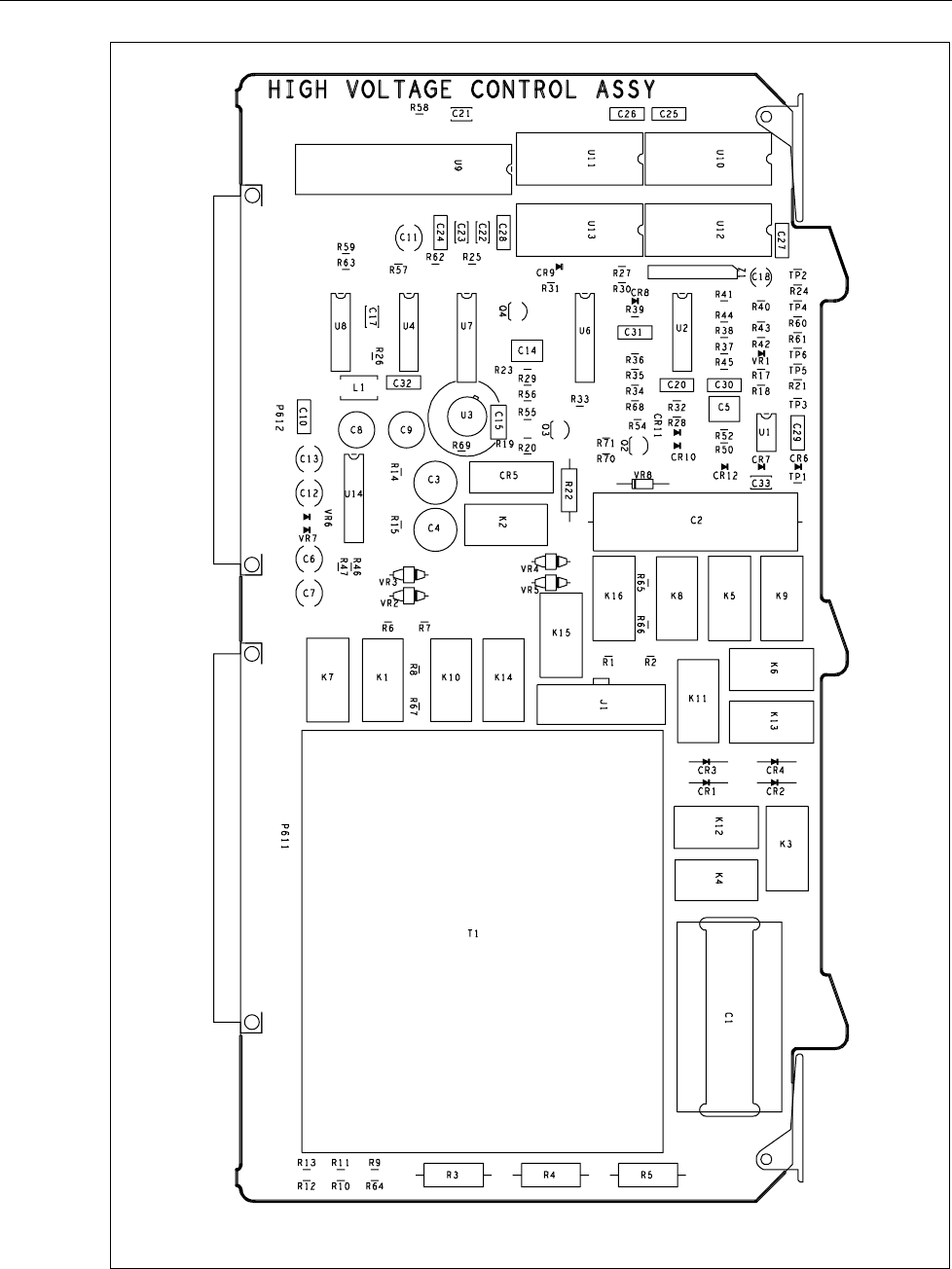
5700A/5720A Series II Calibrator
Service Manual
6-62
5700A-1661
57001661.EPS
Figure 6-20. A14 High Voltage Control PCA

List of Replaceable Parts
Service Centers
6
6-63
Table 6-19. A15 High Voltage/High Current PCA
Reference
Designator Description Fluke Stock
No Tot Qty Notes
C2,C29,C42 CAP,POLYES,0.01UF,+-10%,50V 715037 3
C4 CAP,POLYPR,0.022UF,+-5%,1500V 806968 1
C5,C15-17,C20,
C21 C23-28,C32
C33,C35,C38,C40
CAP,POLYES,0.1UF,+-10%,50V 649913
649913
649913
17
C6 CAP,POLYES,0.047UF,+-10%,50V 820548 1
C7 CAP,CER,180PF,+-2%,50V,C0G 820522 1
C8 CAP,CER,680PF,+-5%,50V,C0G 743351 1
C10 CAP,CER,82PF,+-2%,50V,C0G 714857 1
C11 CAP,CER,47PF,+-20%,50V,C0G 706705 1
C12,C13,C43 CAP,POLYES,0.47UF,+-10%,50V 697409 3
C14,C19 CAP,TA,2.2UF,+-10%,35V 697433 2
C18 CAP,CER,100PF,+-5%,50V,C0G 831495 1
C22 CAP,POLYES,0.01UF,+-10%,50V 715037 1
C30,C31,C37,C39 CAP,TA,10UF,+-20%,35V 816512 4
C34 CAP,TA,22UF,+-20%,10V 658971 1
C41 CAP,POLYES,0.22UF,+-10%,50V 706028 1
CR1,CR4 CR11-
16,CR24,CR25
*
*
DIODE,SI,BV=75V,IO=150MA,500MW 203323
203323
10
CR2,CR17,CR18,
CR20,CR21
*
*
DIODE,SI,N-JFET,CURRENT REG,IF 852116
852116
5
CR5,CR6,CR9,
CR10 CR22,
CR23
DIODE,SI,100 PIV,1 AMP 742874
742874
742874
6
CR19 * DIODE,SI,N-JFET,CURRENT REG,IF 852124 1
H1,H2 SCREW,PH,P,LOCK,SS,6-32,.500 320051 2 1
H4 * HYBRID ASSEMBLY, TESTED 813444 1
H6-10,H21 SCREW,PH,P,LOCK,STL,6-32,.250 152140 6
H17-20 RIVET,S-TUB,OVAL,AL,.087,.343 838458 4
HR7 * HIGH VOLTAGE DC HYBRID 775254 1
K1 RELAY,ARMATURE,4 FORM C,5V,LATCH 715078 1
K2,K3 RELAY,ARMATURE,2 FORM C,5V,LATCH 769307 2
K4,K5,K8,K9,K12 RELAY,ARMATURE,2 FORM C,5V 733063 5
K6,K7,K10,K11,
K14
RELAY,ARMATURE,1 FORM A/1 FORM 831545
831545
5
L4,L5 CHOKE,6TURN 320911 2
MP1,MP2 EJECTOR,PWB,NYLON 494724 2
MP3 SHIELD, HIGH VOLTAGE, REAR 791921 1
MP4 MOLDED COVER, REF. HYBRID 797746 1
MP5 MOLDED COVER, HYBRID, R-NET 775619 1
MP6-9 SPACER,BROACH,SNAP,BR,1.062 832469 4
MP10 THERMAL INSULATOR, HIGH VOLTAG 797829 1 1
MP11,MP12 INSUL PT,TRANSISTOR MOUNT,DAP,T0-5 152207 2
MP14-16 CABLE TIE,5",1.375"DIA 807230 3
MP22 HI VOLT CLAMP BAR 760850 1 1
P601,P602 CONN,DIN41612,TYPE C,RT ANG,64 PIN 807800 2
Q3,Q13 * TRANSISTOR,SI,NPN,SMALL SIGNAL 346916 2
Q4,Q15,Q22,Q23 * TRANSISTOR,SI,NPN,SMALL SIGNAL 698225 4
Q6,Q12 * TRANSISTOR,SI,PNP,SMALL SIGNAL 402586 2
Q8,Q18 * TRANSISTOR,SI,BV=40V,40W,TO-220 369660 2
Q9,Q19 * TRANSISTOR,SI,BV=60V,65W,TO-220 386128 2
Q10 * TRANSISTOR,SI,P-JFET,TO-92 852111 1
Q11 * TRANSISTOR,SI,BV=100V,50W,TO-220 454041 1 1
Q14 * TRANSISTOR,SI,BV=100V,40W,TO-220 454033 1 1
Q16,Q24 * TRANSISTOR,SI,PNP,40V,0.35W,TO-92 698233 2
Q20,Q21 * TRANSISTOR,SI,N-JFET,SEL,TO-92 707703 2

5700A/5720A Series II Calibrator
Service Manual
6-64
Table 6-19. A15 High Voltage/High Current PCA (cont)
Reference
Designator Description Fluke Stock
No Tot Qty Notes
R1,R72 RES,CF,1K,+-5%,0.25W 343426 2
R2,R15,R39 RES,CF,100K,+-5%,0.25W 348920 3
R4,R11,R51 R53,
R61-64,R74
RES,CF,100,+-5%,0.25W 348771
348771
9
R5 RES,CF,1.5K,+-5%,0.25W 810432 1
R6,R9 RES,CF,1M,+-5%,0.25W 348987 2
R7 RES,CF,51K+-5%,0.25W 747550 1
R8,R19 RES,CF,3K,+-5%,0.25W 441527 2
R10 RES,CF,820,+-5%,0.25W 442327 1
R12 RES,CF,33K,+-5%,0.25W 733667 1
R13 RES,MF,34.8K,+-1%,0.125W,100PPM 772319 1
R14,R16,R21,
R27,R28,R40,
R44,R52,R54, R71
RES,CF,10K,+-5%,0.25W 348839
348839
348839
348839
10
R17,R41 RES,CF,4.7K,+-5%,0.25W 348821 2
R18 RES,CF,22K,+-5%,0.25W 348870 1
R20 RES,CF,1.5K,+-5%,0.25W 343418 1
R22 RES,CF,16K,+-5%,0.25W 442376 1
R23,R24,R60, R65 RES,CF,10,+-5%,O.25W 340075
340075
4
R25,R26 RES,MF,14.3,+-1%,0.125W,100PPM 447144 2
R29,R30 RES,CF,8.2K,+-5%,0.25W 441675 2
R31,R32 RES,CC,2K,+-5%,0.5W 640729 2
R33-35 RES,CC,470,+-10%,0.5W 641081 3
R36 RES,CF,47,+-5%,0.25W 441592 1
R37,R38 RES,MF,825,+-1%,0.125W,100PPM 294892 2
R42,R43,R45, R46 RES,MF,10K,+-1%,0.125W,100PPM 168260
168260
4
R47 RES,CF,160,+-5%,0.25W 441410 1
R48,R50 RES,MF,2.21K,+-1%,0.125W,100PPM 347476 2
R56,R69 RES,MF,191,+-1%,0.125W,100PPM 325639 2
R57,R68,R77, R78 RES,WW,.1,+-3%,.7W 255679
255679
4
R58,R67 RES,CF,330K,+-5%,0.25W 376640 2
R59,R66 RES,CF,68,+-5%,0.25W 414532 2
R73,R75 RES,CF,2K,+-5%,0.25W 441469 2
R76 RES,CF,3.3,+-5%,0.25W 348730 1
R79,R82 RES,CF,1K,+-5%,0.25W 780585 2
R80,R83 RES,CF,4.7K,+-5%,0.25W 721571 2
R81,R84 RES,CF,10K,+-5%,0.25W 697102 2
TP1,TP3-11 JUMPER,WIRE,NONINSUL,0.200CTR 816090 10
TP2 SOCKET,SINGLE,PWB,FOR 0.080 PIN 170480 1
U1 * IC,OP AMP,JFET INPUT,22V SUPPLY,DIP 832584 1
U2,U4,U5 * IC,OP AMP,JFET INPUT,8 PIN DIP 472779 3
U3 * IC,OP AMP,DUAL,LO OFFST,VOLT,LO-DRIFT 685164 1
VR1,VR2,VR5,
VR6
*
*
ZENER,UNCOMP,16.0V,5%,15.5MA,1.0W 313221
313221
4
VR3,VR4 * ZENER,UNCOMP,20.0V,5%,6.2MA,0.4W 180463 2
VR7,VR8 * ZENER,UNCOMP,16.0V,5%,7.8MA,0.4W 325837 2
W1 CABLE ASSEMBLY, HIGH VOLTAGE 8.125” 881862 1
W2,W3 CABLE ASSEMBLY, HIGH VOLTAGE 7.375” 881859 2
Z5 * R-NET/HEAT SINK ASSY-4R03 761288 1
Z6 * R-NET/HEAT SINK ASSY-4R23 665489 1 1
1. PN 665489 is an assembly containing part numbers 761296, 797829, 454041, 454033, 760850, and 320051
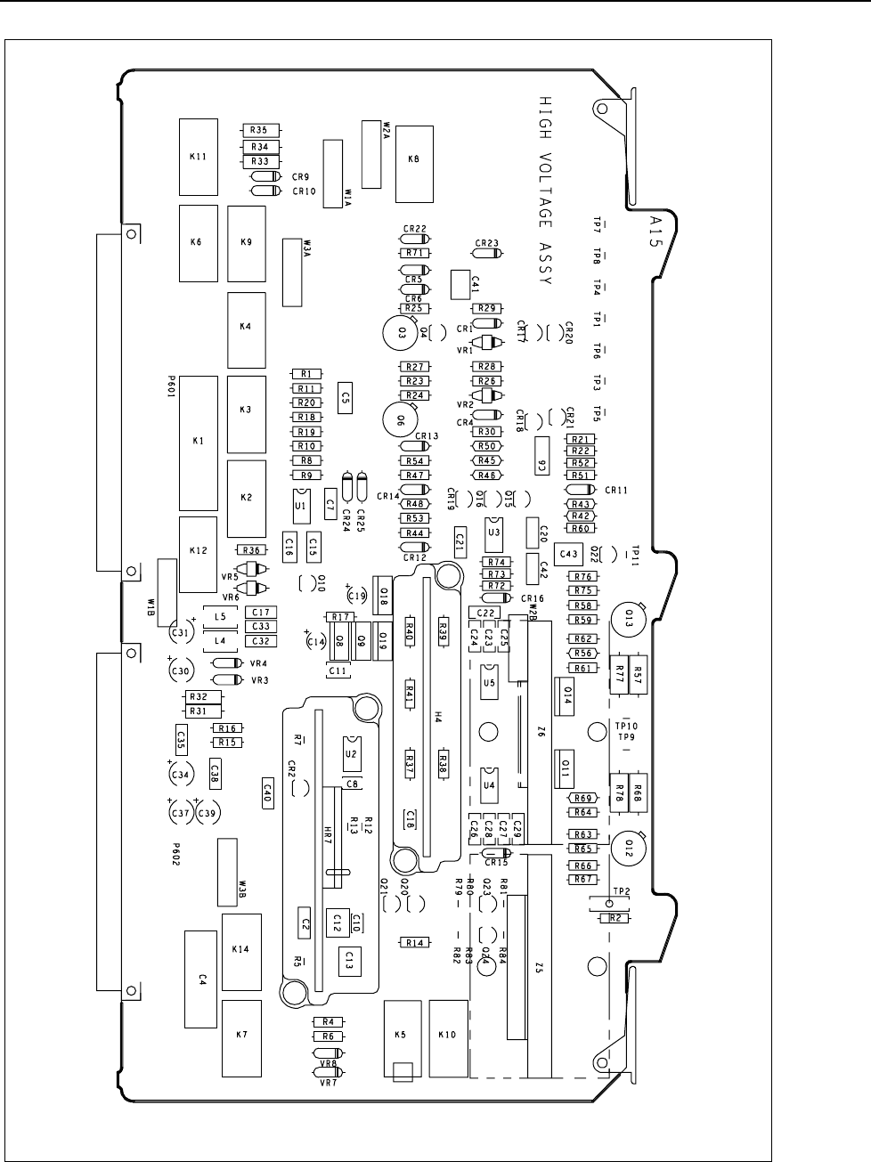
List of Replaceable Parts
Service Centers
6
6-65
5700A-1660
57001660.EPS
Figure 6-21. A15 High Voltage/High Current PCA

5700A/5720A Series II Calibrator
Service Manual
6-66
Table 6-20. A16 Power Amplifier PCA
Reference
Designator Description Fluke Stock
No Tot Qty Notes
C1,C2 CAP,CER,10PF,+-10%,3000V,C0G 817049 2
C3 CAP,MICA,560PF,+-5%,500V 170431 1
C4,C28 CAP,CER,0.02UF,+-20%,500V,Z5U 407403 2
C5,C75 CAP,POLYES,0.047UF,+-10%,50V 820548 2
C6,C17,C23 CAP,CER,22PF,+-10%,1000V,C0G 817023 3
C7,C24,C43 CAP,CER,1000PF,+-20%,50V,X7R 697458 3
C8,C13,C16,C20,
C47,C49,C60,C61,
C68-71
CAP,POLYES,0.22UF,+-5%,50V 747519
747519
747519
12
C9,C21 CAP,TA,15UF,+-20%,20V 807610 2
C10,C25 CAP,TA,1UF,+-20%,35V 697417 2
C11 CAP,CER,22PF,+-2%,50V,C0G 714832 1
C12 CAP,CER,2000PF,+-5%,50V, C0G 832618 1
C15 CAP,CER,0.01UF,+80-20%,500V,Z5 816991 1
C18 CAP,CER,6.8PF,+-0.1PF,500V,C0J 485383 1
C19 CAP,CER,100PF,+-5%,50V,C0G 831495 1
C22 CAP,MICA,2PF,+-0.5PF,500V 175208 1
C26 CAP,CER,1000PF,+-20%,3000V,Z5U 832709 1
C27,C78,C79 CAP,AL,3.3UF,+30-20%,450V 782524 3
C31-34 CAP,AL,22UF,+-20%,35V 817056 4
C40 CAP,POLYES,1UF,+-10%,50V 733089 1
C41 CAP,POLYPR,0.15UF,+-10%,400V 557504 1
C42 CAP,CER,470PF,+-10%,50V,C0G 733071 1
C45 CAP,TA,2.2UF,+-10%,35V 697433 1
C48,C72 CAP,CER,1.2PF,+-0.25PF,50V,C0K 715235 2
C57 CAP,CER,100PF,+-10%,1000V,S3N 816983 1
C65,C67 CAP,TA,4.7UF,+-20%,25V 807644 2
C73 CAP,CER,0.05UF,+80-20%,500V,Z5 105676 1
C74 CAP,POLYES,0.1UF,+-10%,50V 649913 1
C80,C81 CAP,POLYES,0.47UF,+-10%,50V 697409 2
C82 CAP,CER,10PF,+-2%,50V,C0G 713875 1
CR1-5,CR7,CR10,
CR12-014,CR16,
CR20,CR21,CR23-
025,CR27,CR29-
31,CR61-67
*
*
*
*
*
DIODE,SI,BV=75V,IO=150MA,500MW 659516
659516
659516
659516
659516
27
CR8,CR9 DIODE,SI,100 PIV,1 AMP 887203 2
CR18,CR19 * DIODE,SI,BV=125V,IO=150MA,500 MW 844647 2
CR33,CR68,
CR69
*
*
DIODE,SI,N-JFET,CURRENT REG,IF 852116
852116
3
CR35-39 DIODE,SI,BV=200V,IO=200MA 876867 5
CR53 * DIODE,SI,N-JFET,CURRENT REG,IF 334839 1
H1,H2 SCREW,PH,P,LOCK,SS,6-32,.500 320051 2
H3,H4 SCREW,PH,P,LOCK,SS,6-32,.750 376822 2
H10,H48,H59,H60 SCREW,PH,P,LOCK,SS,6-32,.375 334458 4
H13-16 RIVET,S-TUB,OVAL,AL,.087,.343 838458 4
HR8 * POWER AMP DC HYBRID 775437 1
K1,K2 RELAY,ARMATURE,4 FORM C,5V,LATCH 715078 2
K3,K4 RELAY,ARMATURE,2 FORM C,5V,LATCCH 769307 2
K10,K11,K13-16 RELAY,ARMATURE,2 FORM C,5V 733063 6
K12,K17 RELAY,ARMATURE,2 FORM C,5VDC,HI IR 1278765 2
L1-3 CHOKE,6TURN 320911 3
L10 INDUCTOR,1.5UH,+-5%,128MHZ,SHLD 413856 1
L12 CHOKE,2TURN 417196 1
M17 OSCILLATOR THERMAL COVER 797696 1
MP4 MOLDED COVER, HYBRID, R-NET 775619 1
MP5-6 HEAT DISSIPATOR,DPAK,10 C/W,SM,.315,.900,.400 1599214 2

List of Replaceable Parts
Service Centers
6
6-67
Table 6-20. A16 Power Amplifier PCA (cont)
Reference
Designator Description Fluke Stock
No Tot Qty Notes
MP7-8 HEAT DIS,PRESS ON,TO-5 418384 2
MP20-23 INSUL PT,TRANSISTOR MOUNT,DAP,TO-5 152207 4
MP41,MP42,
MP45-47
SCREW,PH,P,LOCK,STL,6-32,.250 152140
152140
5
MP43,MP44 EJECTOR,PWB,NYLON 494724 2
MP49 HEATSINK, POWER AMP 803007 1 1
MP50 SHIELD, HIGH VOLTAGE, REAR 791921 1
MP51-54 INSUL PT,TRANSISTOR,NYL,.4,.61 844837 4 1
MP55 THERMAL INSULATOR, POWER AMP 791988 1 1
MP56,MP57 POWER AMP CLAMP BAR 803015 2 1
MP58 RIVETED AIR DUCT ASSEMBLY 764506 1
P701,P702 CONN,DIN41612,TYPE C,RT ANG,64 PIN 807800 2
Q1,Q3 TRANSISTOR,SI,N-MOS,40W,500V,T0-220 782540 2 1
Q2 * TRANSITOR,SI,N-JFET,UHF/VHF US 851972 1
Q4,Q7,Q32 Q60,
Q62
*
*
TRANSISTOR,SI,NPN,SMALL SIGNAL 698225
698225
5
Q5 * TRANSISTOR,SI,NPN,HI-FREQ,T0-39 912522 1
Q6 * TRANSISTOR,SI,PNP,SMALL SIGNAL 844993 1
Q8 * TRANSISTOR,SI,N-DMOS FET,TO-72 394122 1
Q9,Q16,Q54 * TRANSISTOR,SI,NPN SMALL SIGNAL 853478 3
Q10 * TRANSISTOR,SI,PNP,70V,400MA,TO-39 866756 1
Q11 * TRANSISTOR,SI,PNP,SWITCHING,TO-92 831446 1
Q12,Q14 * MOSFET,SI,N,STD1NB80,800V,1A,20 OHMS,1.75W 1599223 2 1
Q13 * TRANSISTOR,SI,P-MOS,500V,TO-92 782508 1
Q15,Q17 * TRANSISTOR,SI,P-MOS,POWER,500V 782482 2 1
Q31 * TRANSISTOR,SI,VMOS,PWR,TO-237,VN10KM 640516 1
Q33,Q34 * TRANSISTOR,SI,N-JFET,SEL,TO-92 707703 2
Q35 * TRANSISTOR,SI,BV=60V,65W,TO-220 386128 1
Q38 * TRANSISTOR,SI,BV=40V,40W,TO-220 369660 1
Q39,Q40,Q50,
Q51,Q57,Q58
*
*
TRANSISTOR,SI,N-DMOS PWR FET,T0-92 782565
782565
6
Q61 * TRANSISTOR,SI,PNP,40V,0.35W,TO-92 698233 1
R1 RES,CF,9.1K,+-5%,0.25W 706663 1
R2,R18,R54,R56,
R89,R90,R134,
R135
RES,CF,10K,+-5%,0.25W 697102
697102
697102
8
R3,R4,R81-83 RES,MF,100K,+-0.1%,0.5W,50PPM 369371 5
R5 RES,MF,30.1K,+-1%,0.125W,100PPM 772061 1
R6 RES,CF,51K+-5%,0.25W 747550 1
R7 RES,MF,1.5M,+-1%,0.125W,100PPM 714998 1
R8,R86 RES,MF,10K,+-0.1%,0.125W,50PPM 733972 2
R9,R10,R16,R33,
R40,R50 R59,
R115,R148 R149
RES,MF,1K,+-1%,0.125W,100PPM 816595
816595
816595
10
R11,R12 RES,MF,16.5K,+-1%,0.5W,100PPM 162529 2
R13 RES,MF,17.4K,+-1%,0.5W,100PPM 247270 1
R14,R73,R137 RES,CF,43K,+-5%,0.25W 821777 3
R15,R19,R52, R57 RES,CC,68K,+-10%,1W 686987 4
R17,R53 RES,MF,4.99K,+-1%,0.125W,100PPM 721548 2
R20,R23 RES,CF,3.9K.+-5%,0.25W 810416 2
R22,R109,R133 RES,CF,430,+-5%,0.25W 817577 3
R24,R138 RES,CF,200,+-5%,0.25W 810390 2
R25,R32 RES,CF,750,+-5%,0.25W 810374 2
R26,R126,R128 RES,CF,620,+-5%,0.25W 810408 3
R27 RES,CC,1K,+-5%,0.5W 687811 1

5700A/5720A Series II Calibrator
Service Manual
6-68
Table 6-20. A16 Power Amplifier PCA (cont)
Reference
Designator Description Fluke Stock
No Tot Qty Notes
R28,R29,R34, R47 RES,MF,499K,+-1%,0.125W,100PPM 714980
714980
4
R30 RES,CF,330,+-5%,0.25W 830596 1
R31 RES,CF,100K,+-5%,0.25W 658963 1
R35,R74,R139 RES,CF,20,+-5%,0.25W 810382 3
R36,R141,R151,
R152
RES,CF,47,+-5%,0.25W 822189
822189
4
R37 RES,CF,12K,+-5%,0.25W 757799 1
R38,R118 RES,CF,47K,+-5%,0.25W 721787 2
R41,R51,R55 RES,CC,200K,+-5%,1W 686774 3
R46,R108 R110-
113
RES,CF,100,+-5%,0.25W 810465
810465
6
R58 RES,CF,33,+-5%,0.25W 414524 1
R61 RES,CF,750K,+-5%,0.25W 747543 1
R84 RES,MF,22.1K,+-1%,0.125W,100PPM 655266 1
R85 RES,CC,27M,+-5%,0.25W 875257 1
R87 RES,MF,84.5,+-1%,0.125W,100PPM 236851 1
R88,R97,R98 RES,MF,10,+-1%,0.125W,100PPM 820399 3
R92 RES JUMPER,0.02,0.25W 682575 1
R116,R129 RES,CF,4.7K,+-5%,0.25W 721571 2
R117 RES,CF,24K,+-5%,0.25W 697599 1
R120 RES,CC,47,+-5%,0.5W 644259 1
R125 RES,CF,2K,+-5%,0.25W 810457 1
R132 RES,MF,20K,+-0.1%,0.25W,25PPM 810564 1
R142 RES,CF,200K,+-5%,0.25W 681841 1
R143 RES,CF,300K,+-5%,0.25W 732818 1
R144 RES,CF,1K,+-5%,0.25W 780585 1
R146,R147 RES,CF,2.4,+-5%,0.25W 348508 2
R150 RES,CF,15,+-5%,0.25W 348755 1
TP1-5,TP7-13,
TP16,TP17
JUMPER,WIRE,NONINSUL,0.200CTR 816090
816090
14
TP6 SOCKET,SINGLE,PWB,FOR 0.080 PIN 170480 1
TP14 SOCKET,SINGLE,PWB,FOR 0.080 PIN 149138 1
TP15 SOCKET,SINGLE,PWB,FOR 0.080 PIN 149120 1
U1 * IC,OP AMP,PRGRBL OUT CURRNT,8 PIN 418913 1
U2,U5 * IC,CMOS,QUAD BILATERAL SWITCH 910708 2
U4 * IC,OP AMP,HIGH SPEED,LOW NOISE 875815 1
U7 * IC,OP AMP,JFET INPUT,22V SUPPLY,DIP 832584 1
U8 * IC,CMOS,HEX INVERTER 381848 1
U9 * IC,OP AMP,CHOPPER STABLIZED,8 PIN 831263 1
U10 * IC,BPLR,FAHRENHEIT TEMPERTURE 845156 1
VR6,VR11,VR19,
VR22 VR26,VR28
VR32
*
*
*
ZENER,UNCOMP,10.0V,5%,12.5MA,0.4W 810267
810267
810267
7
VR15 * ZENER,UNCOMP,18.0V,5%,7.0MA,0.4W 827973 1
VR18 * ZENER,UNCOMP,15.0V,5%,8.5MA,0.4W 266601 1
VR51,VR52,VR57,
VR58
*
*
ZENER,UNCOMP,6.8V,5%,20.0MA,0.4W 260695 4
VR61,VR62 * ZENER,UNCOMP,3.3V,5%,20.0MA,0.4W 820423 2
VR64 * ZENER,UNCOMP,24.0V,5%,20MA,0,4W 267807 1
VR65 * ZENER,UNCOMP,8.2V,5%,20MA,0.4W 386771 1
Z1 * RNET,MF,HERM,SIP,5700 HI V DIVIDER 764399 1
1. Part number 665570 is an assembly consisting of part numbers 803007, 791988, 782482, 782540, 844837, 334458, 803015 and 320051
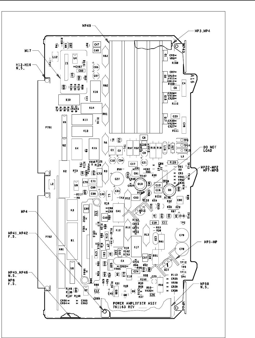
List of Replaceable Parts
Service Centers
6
6-69
5700A-7670
57001670.EPS
Figure 6-22. A16 Power Amplifier PCA

5700A/5720A Series II Calibrator
Service Manual
6-70
Table 6-21. A16A1 Power Amplifier Digital Control SIP PCA
Reference
Designator Description Fluke Stock
No Tot Qty Notes
C52 CAP,AL,15UF,+-20%,35V 614024 1
C53,C56 CAP,CER,33PF,+-5%,50V,C0G 714543 2
C54 CAP,CER,470PF,+-10%,50V,C0G 733071 1
C55,C57 CAP,POLYES,0.22UF,+-5%,50V 747519 2
L4 CHOKE,6TURN 320911 1
MP3 HEADER,2 ROW,.100CTR,RT ANG,10 PIN 658112 1
P1,P2 HEADER,2 ROW,.100CTR,RT ANG,26 PIN 512590 2
R2,R106 RES,CF,1K,+-5%,0.25W 780585 2
R101,R105 RES,MF,1K,+-1%,0.125W,100PPM 816595 2
R102 RES,CF,16K,+-5%,0.25W 714303 1
R103 RES,CF,10K,+-5%,0.25W 697102 1
R104 RES,CF,4.7K,+-5%,0.25W 721571 1
U9 * IC,LSTTL,3-8 LINE DCDR W/ENABL 407585 1
U10,U12 * IC,BIMOS,8 CHNL HI-VOLT DRVR W/LATCH 782912 2
U11 * IC,CMOS,PROGRMBL PERIPHERAL INTERFACE 780650 1
U13,U15 * IC,COMPARATOR,QUAD,14 PIN DIP 387233 2
U14 * IC,CMOS,8-1 LINE MUX/DEMUX ANALOG,SW 836304 1
Z1 RES,CERM,SIP,10 PIN,9 RES,47K,+-2% 485193 1
Z2 RES,CERM,SIP,10 PIN,9 RES,4.7K,+-2% 484063 1
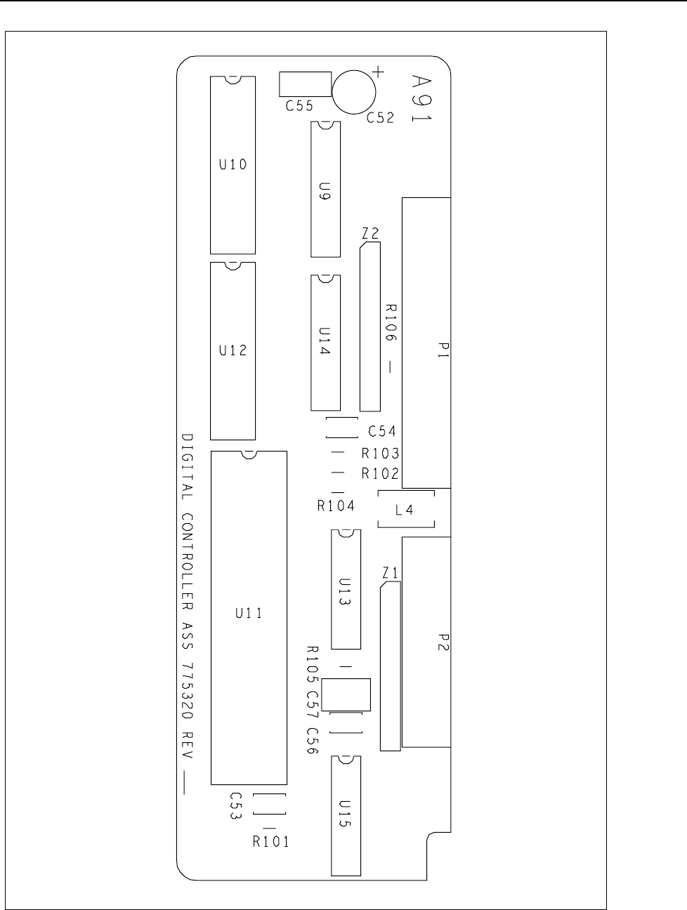
List of Replaceable Parts
Service Centers
6
6-71
5700A-1671
Figure 6-23. A16A1 Power Amplifier Digital Control SIP PCA

5700A/5720A Series II Calibrator
Service Manual
6-72
Table 6-22. A17 Regulator/Guard Crossing PCA
Reference
Designator Description Fluke Stock
No Tot Qty Notes
C1,C2,C4,C6,
C7,C9 C11,C12,
C14-16,C19-23,
C27,C28
CAP,AL,10UF,+-20%,50V,SOLV PROOF 799437
799437
799437
799437
18
C3,C10,C18,C25 CAP,CER,0.05UF,+-20%,100V,Z5V 149161 4
C5,C24,C29, C102 CAP,AL,22UF,+-20%,35V,SOLV PROOF 851766
851766
4
C8,C13 CAP,TA,22UF,+-20%,25V 845149 2
C17,C26,C65, C66 CAP,AL,10UF,+-20%,63V,SOLV PROOF 816843
816843
4
C52,C53 CAP,CER,15PF,+-20%,50V,C0G 697524 2
C54,C56,C59,
C60,C101 C104-
107,C109,C110,
C112-114
CAP,POLYES,0.1UF,+-10%,50V 649913
649913
649913
649913
14
C55,C58 CAP,TA,10UF,+-20%,10V 714766 2
C57 CAP,TA,47UF,+-20%,10V 733246 1
C61,C62 CAP,CER,22PF,+-5%,50V,C0G 714550 2
C63,C64 CAP,CER,100PF,+-2%,50V,T2J 362665 2
C67-70 CAP,TA,22UF,+-20%,25V 357780 4
CR1-34 DIODE,SI,100 PIV,1 AMP 742874 34
CR35 * DIODE,SI, 40PIV,1AMP,SCHOTTKY 837732 1
CR36 THYRISTOR,SI,SCR,VBO=200V,8.0A 634147 1
F1 FUSE,8X8.5MM,3.15A,250V,SLOW,RADIAL 832253 1
H19-22 RIVET,S-TUB,OVAL,AL,.087,.343 838458 4
H45-48 SCREW,PH,P,LOCK,SS,6-32,.500 320051 4
H49-52 HEAT DIS ACC,NYL,TO-3 853952 4
H53-60 NUT,EXT LOCK,STL,6-32,.344OD 152819 8
J801,J802 CONN,DIN41612,TYPE C,RT ANG,64 PIN 807800 2
L51 CHOKE, 3 TURN 452888 1
L53,L54 CHOKE,2TURN 417196 2
MP1,MP5,MP13 HEAT DIS,PRESS ON,TO-5 418384 3
MP2-4,MP9, MP37 HEAT DIS,PWB MT,.75X.50X.50,TO-220 816587 5
MP6-8,MP11 HEAT DIS,HORIZ,1.88X1.40X1.25,TO-3 643593 4
MP10 HEAT DIS,SNAP ON,.75,TO-5 853283 1
MP12 HEAT DIS,CLIP,1.00,1.18,.50,TO-220 643353 1
MP14 HEAT DIS,VERT,1.00X.31X.81,TO-220 853395 1
MP35,MP36 EJECTOR,PWB,NYLON 494724 2
MP38 RIVETED,VOLTAGE REGULATOR AIR DUCT 802777 1
MP39-42 INSUL PT,TO-3,SI,1.650,1.140 473165 4
MP59-62 INSUL PT,TRANSISTOR MOUNT,DAP,TO-5 152207 4
MP71,MP72 PAD, ADHESIVE 735365 2
Q1 * TRANSISTOR, SI, BV=60V, 65W, T0-220 559989 1
Q2 * TRANSISTOR,SI,BV=60V,65W,TO-220 386128 1 1
R1,R4 RES,MF,113,+-0.1%,0.125W,100PPM 484238 2
R02,R8 RES,MF,2.67K,+-1%,0.5W,100PPM 161430 2
R5,R11 RES,MF,203,+-0.1%,.125W,100PPM 851191 2
R6 RES,MF,2.61K,+-0.1%,0.125W,100PPM 851571 1
R10 RES,MF,2.67K,+-0.1%,0.125W,25PPM 340596 1
R13 RES,CF,10,+-5%,O.25W 340075 1
R14,R18 RES,MF,150,+-0.1%,0.125W,100PPM 832360 2
R15,R17 RES,MF,5.11K,0.1%,0.5W,100PPM 832378 2
R19 RES,CC,3K,+-5%,0.5W 641115 1
R20,R58 RES,CF,3K,+-5%,0.25W 441527 2
R52 RES,MF,1K,+-1%,0.125W,100PPM 168229 1
R53 RES,CF,10M,+-5%,.25W 875257 1

List of Replaceable Parts
Service Centers
6
6-73
Table 6-22. A17 Regulator/Guard Crossing PCA (cont)
Reference
Designator Description Fluke Stock
No Tot Qty Notes
R54 RES,CF,1.8K,+-5%,0.25W 441444 1
R56 RES,CF,150,+-5%,0.25W 343442 1
R57 RES,CF,100,+-5%,0.25W 348771 1
R60,R61 THERMISTOR,DISC,POS,100,+-20%,25C 851303 2
SW51 SWITCH,PUSHBUTTON,SPST,MOMENTARY 782656 1
T51 RF TRANSFORMER, 8 MHZ 813477 1
TP1,TP4,TP6, TP8
-
010,TP12, TP55
TP58
JUMPER,WIRE,NONINSUL,0.200CTR 816090
816090
816090
9
U1,U5,U10 * IC,VOLT REG,HIGH VOLTAGE 723445 3
U2,U4 * IC,VOLT REG,FIXED,+15 VOLTS,1.5 AMPS 413187 2 2
U3,U9 * IC,VOLT REG,FIXED,-15 VOLTS,1.5 AMPS 413179 2 3
U6 * IC,VOLT REG,ADJ,POS,LOW DROPOUT 851717 1 4
U7 * IC,VOLT REG,ADJ,NEG,LOW DROPOUT 851720 1 5
U8,U11 * IC,VOLT REG,FIXED,+5 VOLTS,1.0 A,TO-3 327981 2 6
U12 * IC,VOLT REG,FIXED,-5 VOLTS,1.5 AMPS 394551 1
U13 * IC,VOLT REG,ADJ,-1.2 TO 47V,TO-39 845276 1
U51 * IC,CMOS,HEX INVERTER,UNBUFFERED 741199 1
U52 * IC,CMOS,OCTL LINE DRVR W/3-ST OUT 741892 1
U53,U54 * IC,CMOS,3-8 LINE DECODER/DEMUX 799478 2
U55 * IC,CMOS,OCTAL BUS TRANSCEIVER 722017 1
U56 * IC,CMOS,8-BIT MPU,2.0 MHZ,256 BYT RAM 876326 1
U57 * IC,TTL,DUAL AND DRVR W/OPEN COLLECTOR 393959 1
U58 * IC,CMOS,PAL,PROG,5700A/5720A,DIP,U058 601955 1
U59,U63 * IC,CMOS,14 STAGE BINARY COUNTER 807701 2
U60 * IC,VOLT SUPERVISOR,4.55V SENSE INPUT 780577 1
U62 * IC,CMOS,8K X 8 STAT RAM,120 NSEC 783332 1
U64 * EPROM, PROGRAMMED, OTP, 5700A INGARD, U064 600137 1
VR1,VR3 * ZENER,UNCOMP,43V,5%,3MA,0.5W 851584 2
VR2,VR4 * ZENER,UNCOMP,10.0V,5%,12.5MA,0.4W 246611 2
VR5,VR6 * ZENER,UNCOMP,5.6V,5%,220.0MA,5.0W 454553 2
X1 SOCKET,IC,24 PIN 812198 1
X3 SOCKET,IC,28 PIN 448217 1
Y51 CRYSTAL,4.9152 MHZ,+/- 0.005%,HC-18/U 800367 1
Y52 CRYSTAL,8.00MHZ QUARTZ HC-18U 707133 1
Z1,Z3 RES,CERM,SIP,8 PIN,4 RES,10K,+-2% 513309 2
Z2 RES,CERM,SIP,10 PIN,5 RES,10K,+-2% 529990 1
Z51 RES,CERM,DIP,16 PIN,15 RES,10K,+-5% 355305 1
Z52 RES,CERM,SIP,8 PIN,4 RES,4.7K,+-2% 573881 1
Z53,Z54 RES,CERM,SIP,10 PIN,5 RES,33,+-2% 622761 2
1. Q2 is an assembly, pn 665445, consisting of part numbers 816587 and 386128
2. U2 and U4 are assemblies, pn 665411, consisting of part numbers 816587 and 413187
3. U3 and U9 are assemblies, pn 665429, consisting of part numbers 816587 and 413179
4. U6 is an assembly, pn 665398, consisting of part numbers 853952, 643593, 473165, 851717, and 152819
5. U7 is an assembly, pn 665406, consisting of part numbers 853952, 643593, 473165, 851720, and 152819
6. U8 and U11 are assemblies, pn 665414, consisting of part numbers 853952, 643593, 473165, 327981, and 152819
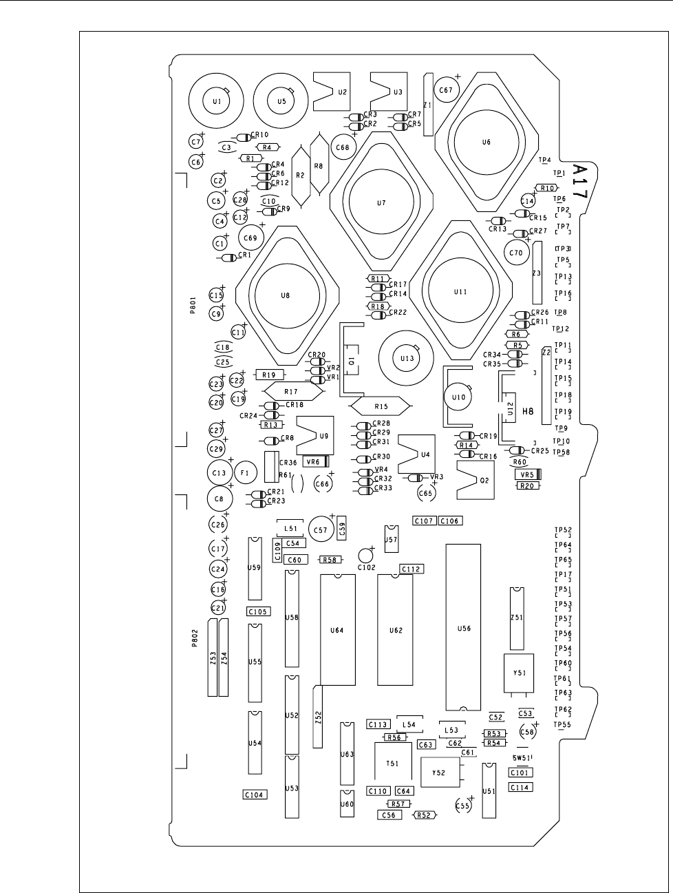
5700A/5720A Series II Calibrator
Service Manual
6-74
5700A-1680
57001680.EPS
Figure 6-24. A17 Regulator/Guard Crossing PCA

List of Replaceable Parts
Service Centers
6
6-75
Table 6-23. A18 Filter/PA Supply PCA
Reference
Designator Description Fluke Stock
No Tot Qty Notes
C1,C10,C17 CAP,POLYES,0.22UF,+-5%,50V 747519 3
C2,C3 CAP,AL,6800UF,+-20%.25V 782466 2
C4,C6 CAP,AL,1000UF,+-20%,50V,SOLV PROOF 782391 2
C5,C19 CAP,AL,2200UF,+-20%,25V,SOLV PROOF 782383 2
C7-9,C18 CAP,AL,330UF,+-20%,100V,SOLV PROOF 816785 4
C11 CAP,AL,220UF,+-20%,25V,SOLV PROOF 816793 1
C12,C22 CAP,AL,22UF,+-20%,35V 817056 2
C13-16 CAP,AL,3300UF,+-20%,50V 782458 4
C20 CAP,AL,10UF,+-20%,63V,SOLV PROOF 816843 1
C21 CAP,AL,470UF,+-20%,50V,SOLV PROOF 747493 1
C23,C209,C210 CAP,POLYES,1UF,+-10%,50V 733089 3
C201,C203, C204,
C206
CAP,AL,47UF,+-20%,400V,SOLV PROOF 782532
782532
4
C202,C205 CAP,AL,3.3UF,+30-20%,450V 782524 2
C207,C208 CAP,AL,100UF,+-20%,16V,SOLV PROOF 816850 2
C211,C212 CAP,CER,100PF,+-5%,50V,C0G 831495 2
CR1,CR2,CR04,
CR5 CR8,CR10,
CR12,CR13
DIODE,SI,150 PIV,5.0 AMP 523720
523720
523720
8
CR3,CR14 DIODE,SI,RECT,BRIDGE,BV=100V,IO=2A 392910 2
CR6,CR7 DIODE,SI,RECT,BRIDGE,BV=200V,I.5A 296509 2
CR9,CR16,CR18 DIODE,SI,100 PIV,1 AMP 742874 3
CR11,CR15,
CR17
DIODE,SI,RECT,BRIDGE,BV=50V,IO=3A 586115
586115
3
CR19 * THYRISTOR,SI,TRIAC,VBO=200V,8.0A 413013 1
CR201,CR203,
CR208,CR210,
CR234,CR235,
CR239,CR243,
DIODE,SI,400 PIV,1 AMP 831586
831586
831586
831586
8
CR205,CR217,
CR218,CR220,
CR221,CR223,
CR224,CR227,
CR228,CR240,
CR247,CR248
DIODE,SI,1K PIV,1.0 AMP 707075
707075
707075
707075
707075
707075
12
CR209,CR236 * DIODE,SI,N-JFET,CURRENT REG,IF 334839 2
CR222 DIODE,SI,RECT,BRIDGE,BV=800V,IO=1A 341016 1
CR244,CR251-
253
*
*
DIODE,SI,BV=75V,IO=150MA,500MW 659516
659516
4
F1,F2,F8 FUSE,8X8.5MM,1.6A,250V,SLOW,RADIAL 816488 3
F3-5,F7,F9 FUSE,8X8.5MM,0.5A,250V,SLOW,RADIAL 831990 5
F6 FUSE,8X8.5MM,0.315A,250V,SLOW,RADIAL 832337 1
F201-204 FUSE,8X8.5MM,0.2A,250V,SLOW,RADIAL 851949 4
H6-9 RIVET,S-TUB,OVAL,AL,.087,.343 838458 4
J201,J202 JUMPER,REC,2 POS,.100CTR,.025 757294 2
K201 RELAY,ARMATURE,2 FORM C,5V 733063 1
MP2 FOOT,RUBBER,ADHES,BLK,.50 SQ,.12 THK 543488 1
MP3 HEAT DIS,PRESS ON,TO-5 418384 1
MP4,MP5 EJECTOR,PWB,NYLON 494724 2
MP10 INSUL PT,TRANSISTOR MOUNT,DAP,TO-5 152207 1
MP201,MP202 HEADER,1 ROW,.100CTR,2 PIN 643916 2
MP203-206 HEAT DIS,VERT,1.00X1.50X.375,T0-220 816546 4
MP207-210 INSUL PT,POWER,SI,.750,.500 534453 4
MP211-214 WASHER,SHOULDER,TEFLON,#4 844824 4
MP215-218 SCREW,PH,P,LOCK,SS,4-40,.250 256156 4
MP219-222 NUT,HEX,STL,4-40 110635 5
P901,P902 CONN,DIN41612,TYPE C,RT ANG,64 PIN 807800 2

5700A/5720A Series II Calibrator
Service Manual
6-76
Table 6-23. A18 Filter/PA Supply PCA (cont)
Reference
Designator Description Fluke
Stock
No
Tot Qty Notes
Q201,Q202 * TRANSISTOR,SI,N-MOS,40W,500V,T0-220 782540 2 1
Q203,Q206 * PNP,2N6520 R05A,TRANSISTOR,SI,PNP,350V,625MW,TO-92 602961 2
Q204,Q209, Q210,
Q212
*
*
TRANSISTOR,SI,P-MOS,500V,TO-92 782508
782508
4
Q205,Q207, Q208,
Q213
*
*
TRANSISTOR,SI,N-DMOS,500V,TO-92 782490
782490
4
Q211,Q214 * TRANSISTOR,SI,NPN,350V,0.625MW,TO-92 853994 2
Q215,Q216 * TRANSISTOR,SI,P-MOS,POWER,500V 782482 2 2
Q217 * TRANSISTOR,SI,100V,10W,TO-202 943803 1
Q218 * TRANSISTOR,SI,NPN,SMALL SIGNAL 698225 1
Q219 * TRANSISTOR,SI,PNP,40V,0.35W,TO-92 698233 1
R1 RESISTOR A73R,RES,CERM,560,+-5%,2W,100PPM 643764 1
R2-5 RESISTOR A52R,RES,CF,20K,+-5%,0.5W 641099 4
R201,R244 RES,CF,8.2,+-5%,0.25W 442269 2
R202,R243 RES,CF,5.1,+-5%,0.25W 441287 2
R203,R241, R256,
R257
RES,CF,9.1K,+-5%,0.25W 706663
706663
4
R204,R253 RES,CF,1.5,+-5%,0.25W 732800 2
R205,R216, R229,
R240
RESISTOR A52R,RES,CF,560K,+-5%,0.5W 640364
640364
4
R206,R239 RES,CF,1M,+-5%,0.25W 649970 2
R207,R209, R237,
R238
RESISTOR A52R,RES,CF,470K,+-5%,0.5W 641107
641107
4
R208,R210, R235,
R236
RESISTOR A73R,RES,CERM,220K,+-5%,3W,100PPM 642428
642428
4
R211 RES,CF,47,+-5%,0.25W 822189 1
R212,R220, R222,
R231, R242
RES,CF,33K,+-5%,0.25W 733667
733667
733667
5
R213,R217,R218,
R230, R232,R245,
R249
RES,CF,10K,+-5%,0.25W 697102
697102
697102
7
R214,R233 RES,CF,200K,+-5%,0.25W 681841 2
R215,R234 RESISTOR A52R,RES,CF,330,+-5%,0.5W 686789 2
R221,R250 RES,CF,82K,+-5%,0.25W 655027 2
R225 RES,CF,100K,+-5%,0.25W 348920 1
R226,R248 RES,MF,3.16K,+-1%,0.125W,100PPM 235291 2
R228,R247 RES,CF,100K,+-5%,0.25W 658963 2
R246,R251 RES,CF,4.7K,+-5%,0.25W 721571 2
R252 RES,CF,300K,+-5%,0.25W 732818 1
R254,R255 RESISTOR A52R,RES,CF,27,+-5%,0.5W 260984 2
RT1,RT2 THERMISTOR,DISC,POSITIVE,50,+-30% 816140 2
TP201 SOCKET,SINGLE,PWB,FOR 0.080 PIN 170480 1
TP204 SOCKET,SINGLE,PWB,FOR 0.080 PIN 149120 1
TP1-22,TP203,
TP205-212
JUMPER,WIRE,NONINSUL,0.200CTR 816090
816090
31
U1 * IC, VOLT REG,FIXED,-5 VOLTS,0.5 AMPS 816322 1
U2 * IC,VOLT REG,FIXED,+5 VOLTS,0.1 AMPS 816355 1
U3 * IC,VOLT REG,FIXED,-18 VOLTS,1.5 AMPS 845474 1
U201 * IC,COMPARATOR,QUAD,14 PIN DIP 387233 1
VR20,VR21 * ZENER,UNCOMP,82.0V,5%,1.5MA,0.5W 844977 2
VR202,VR213,
VR233,VR242
*
*
ZENER 1N5240B A52R,ZENER,UNCOMP,10.0V,5%,20.0MA,0.5W 473744
473744
10
VR206,VR207,
VR218,VR228,
VR237,VR238
*
*
*
ZENER,UNCOMP,10.0V,5%,20.0MA,0.5W 473744
473744
473744
1. Q201, Q202- Assembly 665486 use part numbers 816546, 534453, 782540, 844824, 256156, 110635
2. Q215,Q216- Assembly 665463 use part numbers 816546, 534453, 782482, 844824, 256156, 110635
List of Replaceable Parts
Service Centers
6
6-77
Table 6-23. A18 Filter/PA Supply PCA (cont)
Reference
Designator Description Fluke Stock
No Tot Qty Notes
VR211,VR217,
VR227,VR231
*
*
ZENER,UNCOMP,140.0V,5%,1.8MA,1.0W 340703
340703
4
VR212,VR216,
VR226,VR232
*
*
ZENER,UNCOMP,180V,2%,0.68MA,0.4W 816348
816348
4
VR214,VR230,
VR246,VR247
*
*
ZENER,UNCOMP,56V,5%,2.2MA,0.4W 832568
832568
4
VR215,VR219,
VR225,VR229
*
*
ZENER,UNCOMP,200.0V,5%,5.0MA,5.0W 386839
386839
4
VR245 * ZENER,UNCOMP,3.3V,5%,20.0MA,0.4W 820423 1
Z1-3 RES,CERM,SIP,10 PIN,5 RES,10K,+-2% 529990 3
Z201 RES,CERM,SIP,6 PIN,5 RES,100K,+-2% 412726 1
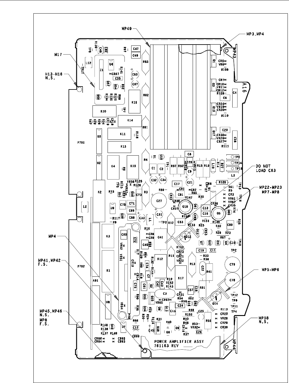
5700A/5720A Series II Calibrator
Service Manual
6-78
5700A-7690
57001690.EPS
Figure 6-25. A18 Filter/PA Supply PCA

List of Replaceable Parts
Service Centers
6
6-79
Table 6-24. A19 Digital Power Supply PCA
Reference
Designator Description Fluke Stock
No Tot Qty Notes
C1 CAP,AL,470UF,+-20%,160V 816835 1
C2 CAP,AL,10UF,+-20%,160V,SOLV PROOF 817064 1
C3 CAP,AL,330UF,+-20%,100V,SOLV PROOF 816785 1
C4,C9 CAP,AL,10UF,+-20%,63V,SOLV PROOF 816843 2
C5,C11 CAP,CER,0.10UF,+-20%,50V,X7R 853650 2
C6 CAP,AL,10000UF,+-20%,25V 816819 1
C7 CAP,AL,6800UF,+-20%.25V 782466 1
C8 CAP,AL,2.2UF,+-20%,50V,SOLV PROOF 816868 1
C10 CAP,AL,22UF,+-20%,35V 817056 1
C12,C13 CAP,AL,22000UF,+-20%,16V 822379 2
C14,C16,C19-23 CAP,CER,0.22UF,+-20%,50V,X7R 853648 7
C15 CAP,AL,100UF,+-20%,16V,SOLV PROOF 816850 1
C17 CAP,POLYPR,0.047UF,+-10%,630V 500827 1
C18 CAP,POLYPR,0.047UF,+-10%,160V 446773 1
C24,C25 CAP,CER,0.022UF,+80-20%,500V,Z5U 740340 2
CR1-4,CR9-12 DIODE,SI,200 PIV,1.0 AMP 586644 8
CR8,CR16, CR21-
24,CR29-34
DIODE,SI,100 PIV,1 AMP 742874
742874
742874
12
CR13 * DIODE,SI,N-JFET,CURRENT REG,IF 852137 1
CR17-20 DIODE,SI,50 PIV,1.0 AMP 379412 4
CR25-28 DIODE,SI,150 PIV,5.0 AMP 523720 4
CR35 * DIODE,GER,BV=66V,IO=50MA 180505 1
F1 FUSE,8X8.5MM,0.315A,250V,SLOW,RADIAL 832337 1
F2 FUSE,8X8.5MM,0.125A,250V,SLOW,RADIAL 832261 1
F3,F4 FUSE,8X8.5MM,2A,250V,SLOW,RADIAL 806331 2
F5 FUSE,8X8.5MM,3.15A,250V,SLOW,RADIAL 832253 1
H2 SCREW,PH,P,LOCK,SS,4-40,.375 256164 1
H3,H4 HEAT DIS,CLIP,1.00,1.18,.50,TO-220 643353 2
H5 HEAT DIS,VERT FINS,TO-3 342675 1
H6,H7 RIVET,S-TUB,OVAL,AL,.087,.343 838458 2
H11 SCREW,PH,P,LOCK,SS,4-40,.437 403782 1
L1-6 CHOKE,6TURN 320911 6
L7 INDUCTOR, 33UH 813485 1
L8 TRANSFORMER, PULSE 660589 1
M1,M2 FOOT,RUBBER,ADHES,GRY,.44 DIA,.20 THK 1601870 2
MP8,MP27 NUT,HEX,STL,4-40 110635 2
MP9,MP10 NUT,EXT LOCK,STL,6-32,.344OD 152819 2
MP11,MP12 GROMMET,SLOT,RUBBER,.438,.062 853291 2
MP13,MP14 EJECTOR,PWB,NYLON 494724 2
MP15,MP26 HEAT DIS,VERT,1.00X1.375X0.50,TO-220 831099 2
MP16 HEAT,DIS,ACC,NYL,TO-3 851907 1
MP21 INSUL PT,POWER,SI,.750,.500 534453 1
MP24 INSUL PT,TO-3,SI,1.650,1.140 473165 1
MP25 INSUL PT,TRANSISTOR MOUNT,DAP,TO-5 152207 1
MP28,MP29 SCREW,PH,P,LOCK,STL,6-32,.250 152140 2
MP30,MP31 SPACER,SWAGE,.250 RND,BR,6-32,.125 435578 2
P41 CONN,DIN41612,TYPE C,RT ANG,64 PIN 807800 1
Q1 * TRANSISTOR,SI,BV=200V,80W,TO-3 261347 1 1
Q2,Q6 * TRANSISTOR,SI,NPN,HI-VOLTAGE 370684 2
Q3,Q7-10 * TRANSISTOR,SI,300V,10W,TO-202 107646 5
Q4 * TRANSISTOR,SI,VCB=200V,1W,TO-3 276899 1
Q5 * TRANSISTOR,SI,BV=60V,65W,TO-220 386128 1
R1 RES,CF,5.1,+-5%,0.25W 441287 1
R2 RES,CF,2K,+-5%,0.25W 441469 1
5700A/5720A Series II Calibrator
Service Manual
6-80
Table 6-24. A19 Digital Power Supply PCA (cont)
Reference
Designator Description Fluke Stock
No Tot Qty Notes
R3,R12 RES,CF,100K,+-5%,0.25W 348920 2
R4 RES,CC,4.7K,+-5%,0.25W 348821 1
R5 RES,CF,12,+-5%,0.25W 442178 1
R6 RES,CC,10K,+-10%,2W 641123 1
R7 RES,CC,2,+-5%,0.5W 641057 1
R8 RES,CF,120K,+-5%,0.25W 441386 1
R9,R11 RES,CF,33K,+-5%,0.25W 348888 2
R10 RES,CF,51K,+-5%,0.25W 376434 1
R13 RES,CC,10K,+-5%,0.25W 148106 1
TP1-5,TP8,TP10,
TP12,TP13
JUMPER,WIRE,NONINSUL,0.200CTR 816090
816090
9
U1 * IC,VOLT REG,FIXED,+12 VOLTS,1.5 AMPS 413195 1 2
U2 * IC,VOLT REG,FIXED,-12 VOLTS,1.5 AMPS 381665 1
U3 * IC,VOLT REG,FIXED,5 VOLTS,2 AMPS 816918 1 3
VR5 * ZENER,UNCOMP,6.2V,5%,20.0MA,0.4W 325811 1
VR6 * ZENER,UNCOMP,36.0V,5%,3.4MA,0.4W 186163 1
VR7 * ZENER,UNCOMP,39.0V,5%,3.2MA,0.4W 831248 1
VR14,VR15 * ZENER,UNCOMP,18.0V,5%,7.0MA,0,4W 327973 2
1. Q1 is a heatsink assembly, part number 665422, consisting of part numbers 261347, 851907, 342672, 473165, and 152819
2. U1 is a heatsink, part number 665471, consisting of part numbers 413195, 831099, 534453, 256164, 110635
3. U3 is a heatsink, part number 665478, consisting of part numbers 816918, 831099, 403782, 110635
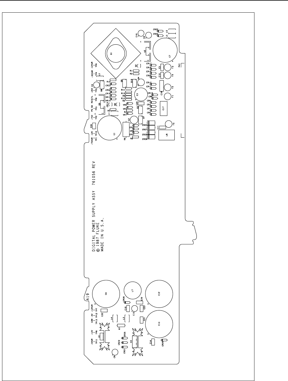
List of Replaceable Parts
Service Centers
6
6-81
5700A-1604
57001604.EPS
Figure 6-26. A19 Digital Power Supply PCA

5700A/5720A Series II Calibrator
Service Manual
6-82
Table 6-25. A20 CPU PCA
Ref Des Description Part
Number
Qty
C1 CAPACITOR SMR,CAP,TA,220UF,+-20%,10V,7343H 106021 1
C2-4,C6-7
C14-16 C18,
C101-111,
C113, C115,
C116, C119-
120, C125-
133, C142-
143, C152
CAPACITOR SMR,CAP,CER,0.1UF,+-10%,50V,X7R,0805 690500 37
C5 CAPACITOR SMR,CAP,TA,15UF,+-20%,35V,7343 690252 1
C8-11 CAPACITOR SMR,CAP,CER,22PF,+-1%,50V,C0G,0805 867663 4
C12-13, C80 CAPACITOR SMR,CAP,CER,0.22UF,+-10%,25V,X7R,1206 106625 3
C17 CAPACITOR SMR,CAP,TA,47UF,+-20%,16V,7343 644994 1
C81 CAPACITOR SMR,CAP,CER,330PF,+-5%,50V,C0G,0805 512038 1
C82 CAPACITOR SMR,CAP,CER,150PF,+-5%,50V,C0G,0805 866533 1
C100 CAPACITOR SMR,CAP,TA,2.2UF,+-20%,20V,3528 854760 1
CR2-3, CR7 DIODE,GF1B SMR,DIODE,SI,100V,1A,DO-214 912451 3
CR4-6, CR8 DIODE,BAT54A SMR,DIODE,SI,SCHOTT,DUAL,30V,200MA,SOT-23 942594 4
DS1 LED,RED,BR1101W,1.6 MCD,20MA,1.7V,1206,TAPE 804788 1
H3-6 RIVET,AL,.089 DIA,.344 L,SEMI-TUBULAR,OVAL HEAD 838458 4
L80-81 INDUCTOR SMR,INDUCTOR,10UH,+-10%,.015ADC 105965 2
MP1 5700A-3006,A-20, MAIN CPU, PCB 1591062 1
P61-62 CONNECTOR ,CONN,DIN41612,TYPE C,RT ANG,64 PIN 802402 2
R1, R3 RESISTOR SMR,RES,CERM,470,+-5%,.125W,200PPM,1206 740506 2
R2, R7 RESISTOR SMR,RES,CERM,0,+.05 MAX,.125W,1206 810747 2
R4 RESISTOR SMR,RES,CERM,10M,+-5%,.125W,400PPM,1206 783274 1
R5 RESISTOR SMR,RES,CERM,1.8K,+-5%,.125W,200PPM,1206 746453 1
R6 RESISTOR SMR,RES,CERM,6.2K,+-5%,.125W,200PPM,1206 746016 1
R8-9 RESISTOR SMR,RES,CERM,75,+-5%,.125W,200PPM,1206 811323 2
R10-16 RESISTOR SMR,RES,CERM,10K,+-1%,.125W,100PPM,1206 769794 7
R51-54 RESISTOR SMR,RES,CERM,5.11K,+-1%,.125W,100PPM,1206 810663 4
R56, R17 RESISTOR SMR,RES,CERM,1K,+-1%,.125W,100PPM,1206 783241 2
R58-59 RESISTOR,CERMET,39.2K,+-1%,0.1W,100PPM,0805,TAPE 943092 2
R60-61 RESISTOR SMR,RES,CERM,1M,+-1%,.125W,100PPM,1206 836387 2
SW1 SWITCH, MICRO, PUSHBUTTON, SPST, MOMENTARY, 24VDC@30MA, SMT, TAPE 1589043 1
T1 TRANSFORMER,SIGNAL,1:1,0.3-150MHZ,1515,TAPE 690669 1
TP1, TP3-14 CONNECTOR,TERMINAL,TEST POINT,1510,TAPE 602125 13
U1 BPLR TL7705A SMR,IC,VOLT SUPERVISOR,5V SENSE,SOIC 780502 1
U2 IC, LOGIC, 74AC05, 2.0V-6.0V, HEX INVERTER W/OPEN DRAIN OUTPUTS, SOIC14, TAPE 1589152 1
U3 CMOS 74HCU04 SMR,IC,CMOS,HEX INVERTER,UNBUFFERED,SOIC 806893 1
U4, U11 IC, LOGIC, 74HC4020, 2.0V-6.0V, 14-STAGE BINARY COUNTER, CLR, SOIC16, TAPE 1589004 2
U5 IC, PLD, ATF22V10C, 5.0V, 500-GATE, EE, PROGRAMMED, U5, SOICW24, TAPE 1609625 1
U6 IC, PLD, ATF22V10C, 5.0V, 500-GATE, EE, PROGRAMMED, U6, SOICW24, TAPE 1609633 1
U8 IC,MICROPROCESSOR,MC68HC000,16 BIT,5V,10 MHZ,PLCC68,TAPE 866777 1
U9 CMOS 74HC32 SMR,IC,CMOS,QUAD 2 INPUT OR GATE,SOIC 783712 1
U10 IC, PLD, ATF22V10C, 5.0V, 500-GATE, EE, PROGRAMMED, U10, SOICW24, TAPE 1609640 1
U13 IC,MEMORY,EEPROM,28C256,256KB,32KX8,5V,250NS,HIGH ENDURANCE,PLCC32,TAPE 1588978 1
U15 IC,MEMORY,FLASH,28F800,8MB,512KX16,5V,80NS,BOTTOM
BOOT,PROGRAMMED,SO44,TAPE
See Note 1 1
List of Replaceable Parts
Service Centers
6
6-83
Table 6-26. A20 CPU PCA (cont)
Ref Des Description Part
Number
Qty
U19 IC,MEMORY,SRAM,7C1021,1MB,64KX16,5V,15NS,TSOP44,TAPE 1609432 1
U25, U27-29 CMOS 74HCT244 SMR,IC,CMOS,OCTL LINE DRVR,SOIC 742593 4
U26, U30 CMOS 74HCT245 SMR,IC,CMOS,OCTAL BUS TRANSCEIVER,SOIC 742577 2
U31 CMOS 68C681 SM,IC,CMOS,DUAL CHANNEL UART,PLCC 866785 1
U32 IC, LOGIC, DS75451, 5.0V, SERIES DUAL PERIPHERAL DRIVERS, SOIC8, TAPE 1589055 1
U33 IC,REAL TIME CLOCK-CALENDAR,ICM7170,5V,PARALLEL,ALARM,SO24,TAPE 1588991 1
U52 BIPOLAR LM324 SMR,IC,OP AMP,QUAD,LOW POWER,SOIC 742569 1
XBT1 CONNECTOR,HOLDER,BATTERY,2450 COIN,SURFACE MOUNT,TAPE 1588957 1
Y1 CRYSTAL,7.3728MHZ,50/100PPM,20PF,PLASTIC ENCAPSULATED,SMD,TAPE 106648 1
Y3 CRYSTAL SMR,CRYSTAL,32.768KHZ,20PPM,SURFACE MT 106754 1
Z1 RESISTOR NETWORK,CERMET,BUSSED,15 RES,16 TERM,3.3K,+-
5%,0.125W,200PPM,4012,TAPE
1589028 1
Z2-3 RESISTOR SMR,RES,CERM,SOIC,16 PIN,15 RES,4.7K,+-2% 838060 2
Z5 RESISTOR SMR,RES,CERM,SOIC,16 PIN,15 RES,100K,+-2% 910745 1
Note 1:
For 5700A, order pn 1608184 for U15.
For 5720A, order pn 1619757 for U15.
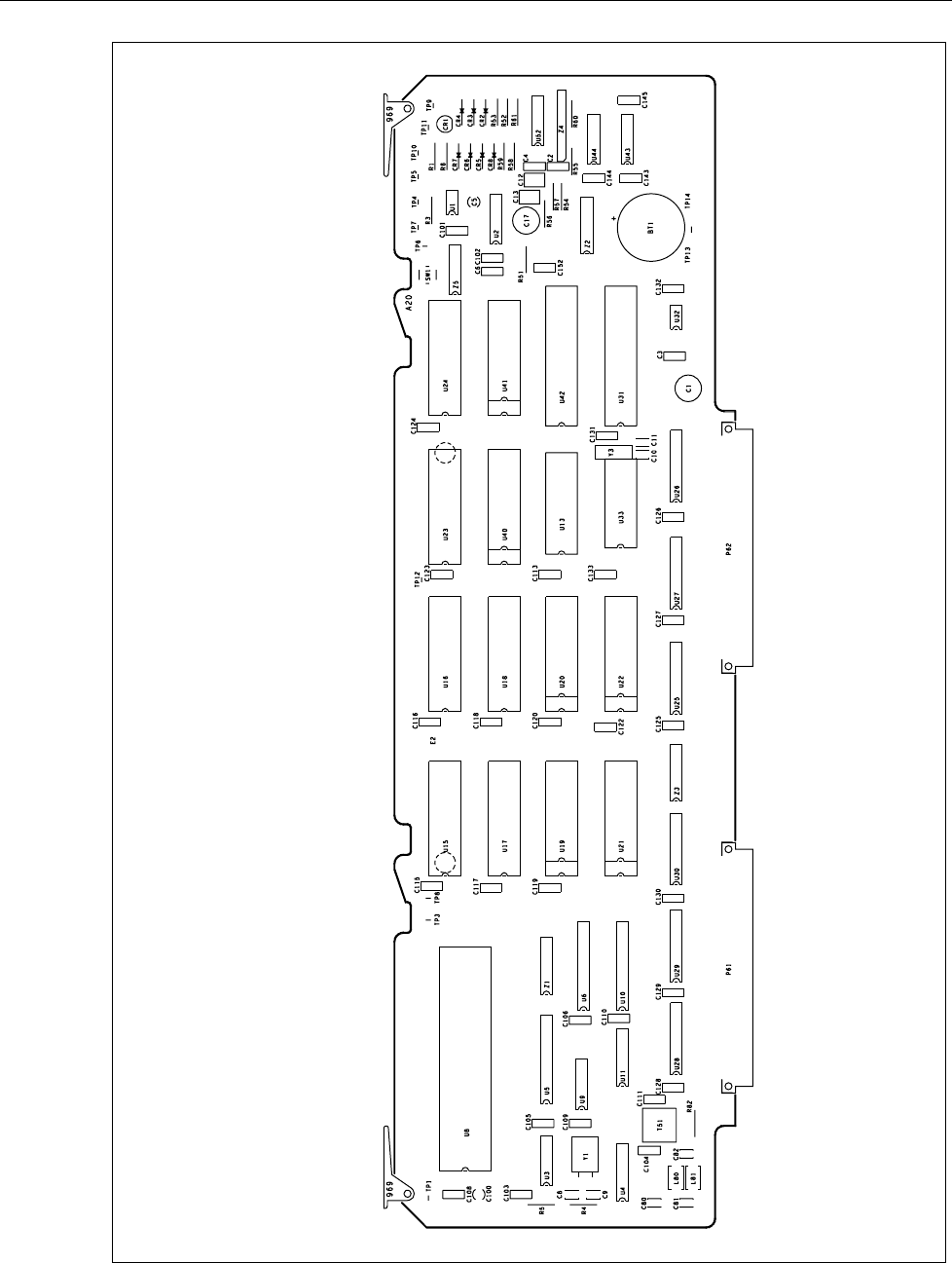
5700A/5720A Series II Calibrator
Service Manual
6-84
57001606.EPS
Figure 6-27. A20 CPU PCA

List of Replaceable Parts
Service Centers
6
6-85
Table 6-27. A21 Rear Panel PCA
Reference
Designator Description Fluke Stock
No Tot Qty Notes
C1,C3,C5 CAP,CER,330PF,+-5%,50V,C0G 697441 3
C4,C21,C22,C24-
32,C34,C36,C37,
C40-45,C48,C49
CAP,POLYES,0.1UF,+-10%,50V 649913
649913
649913
23
C6,C7 CAP,CER,0.22UF,+80-20%,50V,Z5U 649939 2
C8 CAP,CER,4700PF,+-20%,100V,C0G 743427 1
C9 CAP,CER,470PF,+-10%,50V,C0G 733071 1
C10,C70 CAP,TA,68UF,+-20%,15V 193615 2
C11-15 CAP,TA,10UF,+-20%,25V 714774 5
C16 CAP,TA,10UF,+-20%,35V 816512 1
C33 CAP,TA,39UF,+-20%,20V 358234 1
C46,C50 CAP,TA,1UF,+-20%,35V 697417 2
C47 CAP,CER,33PF,+-2%,50V,C0G 715292 1
C71 CAP,CER,47PF,+-20%,50V,C0G 706705 1
CR1-6 * DIODE,SI,BV=75V,IO=150MA,500MW 203323 6
F1,F2 FUSE,.095X.28,0.25A,125V,FAST,AXIAL 806737 2
J1 CONN,MICRO-RIBBON,REC,PWB,24 PIN 851675 1
J2 CONN,D-SUB,PWB,25 PIN 845214 1
J3 CONN,D-SUB,PWB,15 SCKT 837336 1
J4 CONN,D-SUB,PWB,15 PIN 837328 1
J5,J6 CONN,COAX,BNC(F),PWB 479162 2
J7 CONN,D-SUB,PWB,4 CAVITY,32 SCK 810846 1
J8 HEADER,2 ROW,.100CTR,40 PIN 807453 1
J9 HEADER,2 ROW,.100CTR,34 PIN 807446 1
J11,J12 HEADER,1 ROW,.100CTR,3 PIN 837351 2
K1,K4,K5,K7-12 RELAY,ARMATURE,2 FORM C,5V 733063 9
K2,K3,K6 RELAY,ARMATURE,4 FORM C,5V,LATCH 715078 3
L1 CHOKE,6TURN 320911 1
MP1,MP2 SPACER,SWAGE,.250 RND,BR,6-32,.220 261727 2
MP3-10 SPACER,SWAGE,.250 RND,BR,4-40,.234 385310 8
MP21,MP22 SPACER,SWAGE,.250 RND,BR,6-32,.437 423806 2
Q1,Q2 * TRANSISTOR,SI,N-CHAN,TO-92 832139 2
R1 RES,MF,1K,+-1%,0.125W,100PPM 168229 1
R2 RES,MF,332,+-1%,0.125W,100PPM 192898 1
R3 RES,CF,5.1K,+-5%,0.25W 368712 1
R4,R5,R12,R13,
R16,R17
RES,CF,10K,+-5%,0.25W 348839
348839
6
R6 RES,CF,15K,+-5%,0.25W 348854 1
R7,R14 RES,CF,1K,+-5%,0.25W 343426 2
R8,R9 RES,CF,200,+-5%,0.25W 441451 2
R10 RES,CF,620,+-5%,0.25W 810408 1
R11 RES,CC,1K,+-10%,1W 641073 1
R20 RES,CF,200K,+-5%,0.25W 441485 1
R22,R23 RES,MF,200,+-1%,0.125W,100PPM 245340 2
S1 SWITCH,SLIDE,SPDT,LOW PROFILE 911250 1
TP1-15 JUMPER,WIRE,NONINSUL,0.200CTR 816090 15
U1 * IC,CMOS,OCTAL BUS TRANSCEIVER 722017 1
U2 * IC,NMOS,GPIB ADAPTER 585240 1
U3 * IC,LSTTL,OCTAL GPIB XCVR W/OPEN COL 585224 1
U4 * IC,LSTTL,OCTAL IEEE-488 BUS TR 686022 1
U5 * IC,CMOS,DUAL CHANNEL UART (DUART) 799494 1
U6 * IC,TTL,QUAD RS232C LINE DRIVER 1622757 1
U7 * IC,TTL,QUAD RS232C LINE RECEIVER 1622769 1
U8 * IC,CMOS,PAL,PROGRAMD,35NS,5700A-90790 845255 1
U9,U10 * IC,CMOS,OCTL D F/F W/3-STATE,+EDG TRG 585364 2
U11,U12 * IC,CMOS,OCTL LINE DRVR W/3-ST OUT 741892 2

5700A/5720A Series II Calibrator
Service Manual
6-86
Table 6-27. A21 Rear Panel PCA (cont)
Reference
Designator Description Fluke Stock
No Tot Qty Notes
U13 * IC,OP AMP,JFET INPUT,22V SUPPLY,DIP 832584 1
U14 * IC,CMOS,PROGRMBL PERIPHERAL INTERFACE 780650 1
U16,U17 * IC,BIMOS,8 CHNL HI-VOLT DRVR W/LATCH 782912 2
U18 * IC,COMPARATOR,HI-SPEED,14 PIN 647115 1
VR1,VR2 * ZENER,UNCOMP,3.3V,10%,20.0MA,0.4W 309799 2
VR3 * ZENER,UNCOMP,4.7V,10%,20.0MA,0.4W 387084 1
W1 CABLE, BOOST, B-OUT HIGH 802827 1
W2 CABLE, BOOST, B-SENSE HIGH 802850 1
W3 CABLE, BOOST HIGH VOLTAGE 802843 1
X8 SOCKET,IC,24 PIN 812198 1
Z1,Z2 RES,CERM,SIP,10 PIN,9 RES,4.7K,+-2% 484063 2
Z4 RES,CERM,SIP,6 PIN,5 RES,4.7K,+-2% 494690 1
Z5 RES,CERM,SIP,6 PIN,5 RES,10K,+-2% 500876 1
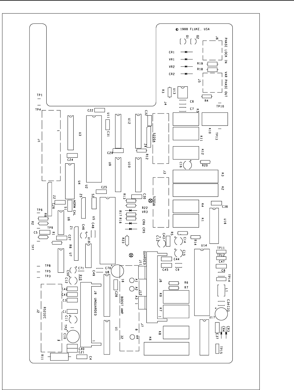
List of Replaceable Parts
Service Centers
6
6-87
5700A-1609
57001609.EPS
Figure 6-28. A21 Rear Panel PCA

5700A/5720A Series II Calibrator
Service Manual
6-88
7-1
Chapter 7
Schematic Diagrams
Figure Title Page
7-1. A1 Keyboard Assembly ......................................................................... 7-3
7-2. A2 Front Panel PCA............................................................................... 7-5
7-3. A3 Analog Motherboard PCA................................................................ 7-10
7-4. A4 Digital Motherboard PCA ................................................................ 7-15
7-5. A5 Wideband Output PCA (Option -03)................................................ 7-19
7-6. A6 Wideband Oscillator PCA (Option -03)........................................... 7-23
7-7. A7 Current/High-Resolution Oscillator PCA ........................................ 7-27
7-8. A8 Switch Matrix PCA .......................................................................... 7-32
7-9. A9 Ohms Cal PCA ................................................................................. 7-38
7-10. A10 Ohms Main PCA ............................................................................ 7-43
7-11. A11 DAC PCA....................................................................................... 7-48
7-12. A11A1 DAC Filter SIP PCA.................................................................. 7-55
7-13. A11A2 DAC Buffered Reference SIP PCA........................................... 7-56
7-14. A12 Oscillator Control PCA .................................................................. 7-57
7-15. A13 Oscillator Output PCA ................................................................... 7-62
7-16. A13A1 Oscillator Wideband SMD PCA................................................ 7-65
7-17. A14 High Voltage Control PCA ............................................................ 7-67
7-18. A15 High Voltage/High Current PCA ................................................... 7-72
7-19. A16 Power Amplifier PCA .................................................................... 7-75
7-20. A16A1 Power Amplifier Digital Control SIP PCA ............................... 7-79
7-21. A17 Regulator/Guard Crossing PCA ..................................................... 7-81
7-22. A18 Filter/PA Supply PCA.................................................................... 7-84
7-23. A19 Digital Power Supply PCA............................................................. 7-87
7-24. A20 CPU PCA........................................................................................ 7-89
7-25. A21 Rear Panel PCA.............................................................................. 7-95
7-26. Hybrids................................................................................................... 7-101

5700A/5720A Series II Calibrator
Service Manual
7-2
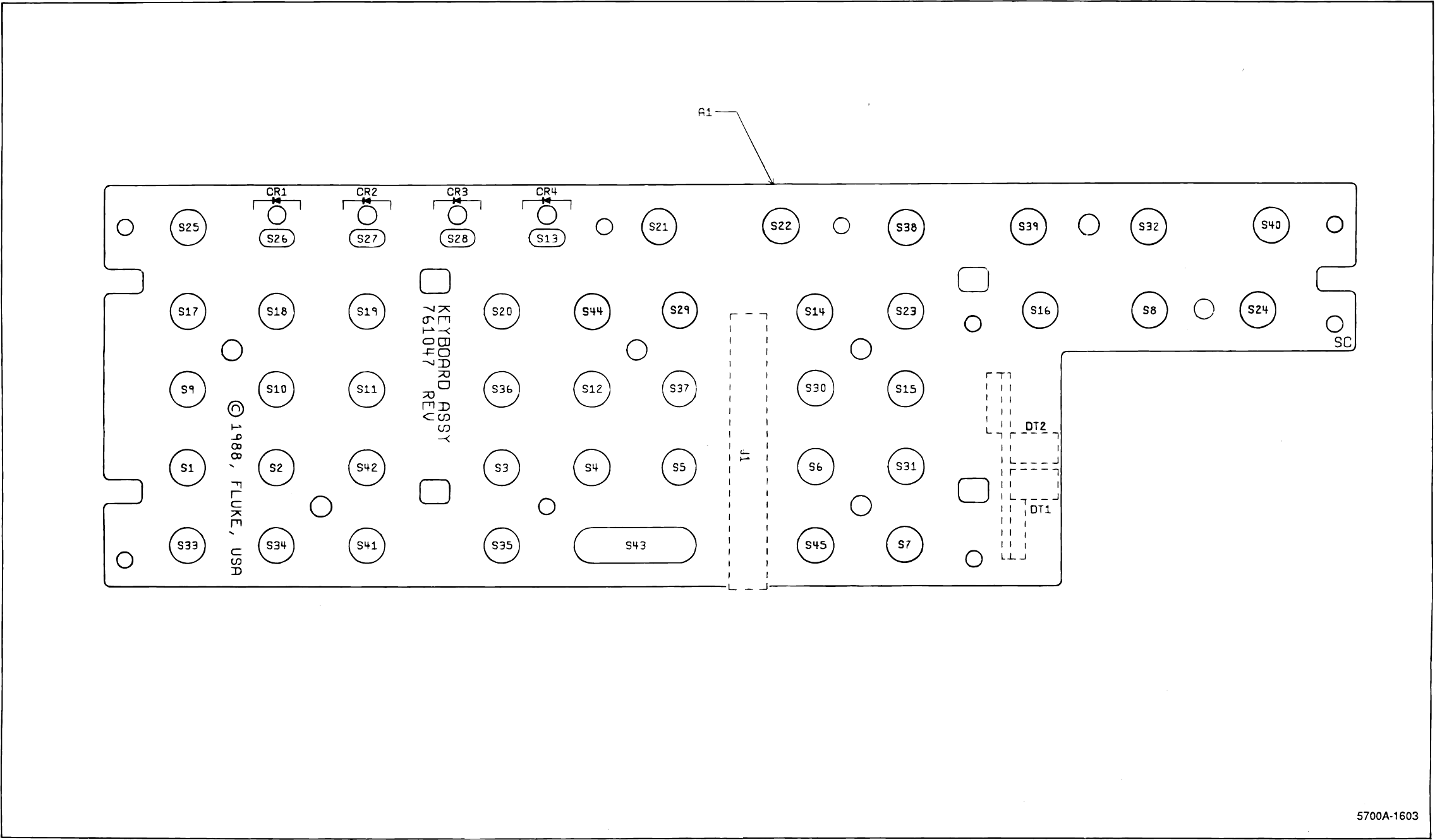
7
Schematic Diagrams
7-3
Figure 7-1. A1 Keyboard PCA
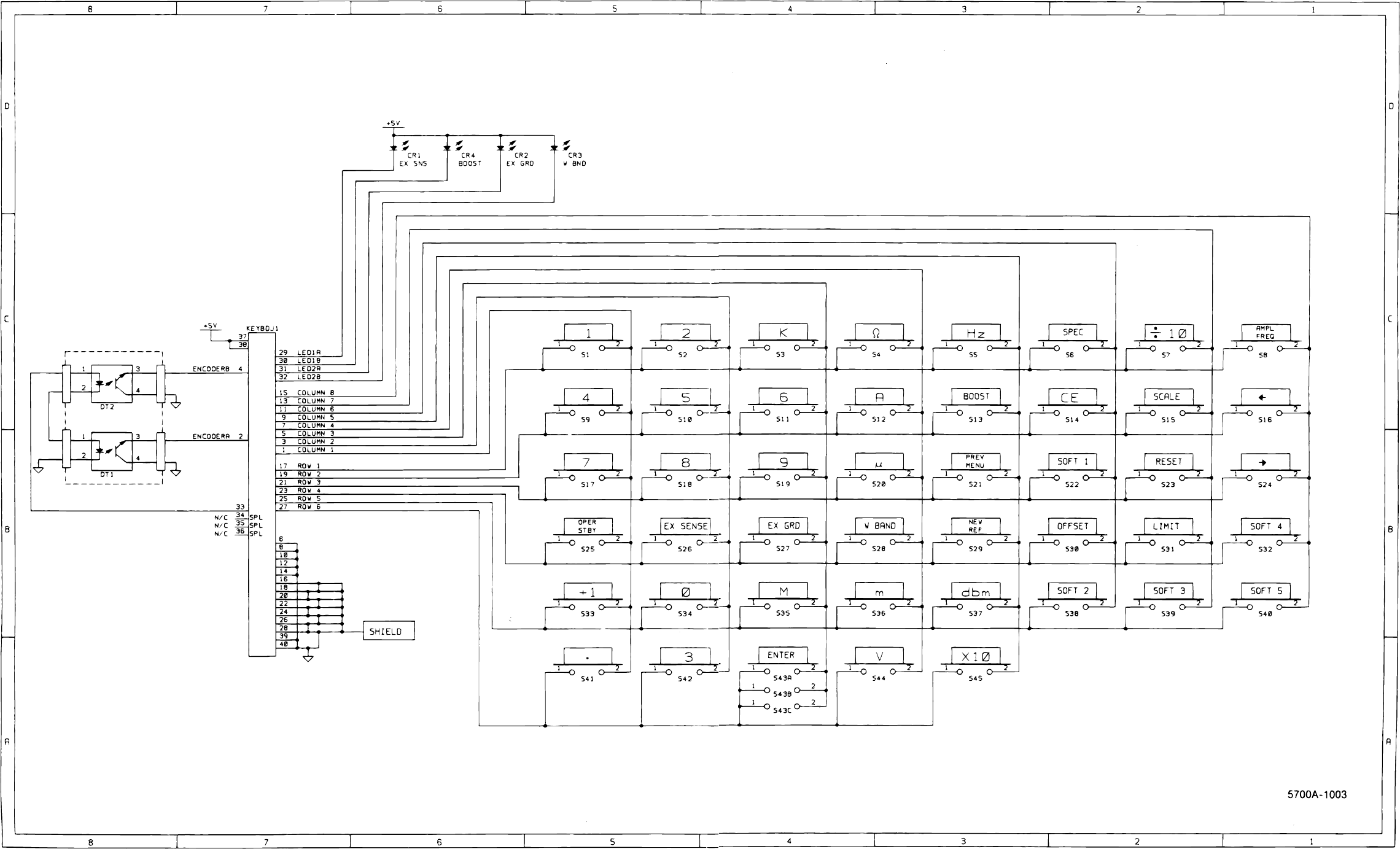
5700A/5720A Series II
Service Manual
7-4
Figure 7-1. A1 Keyboard PCA (cont)
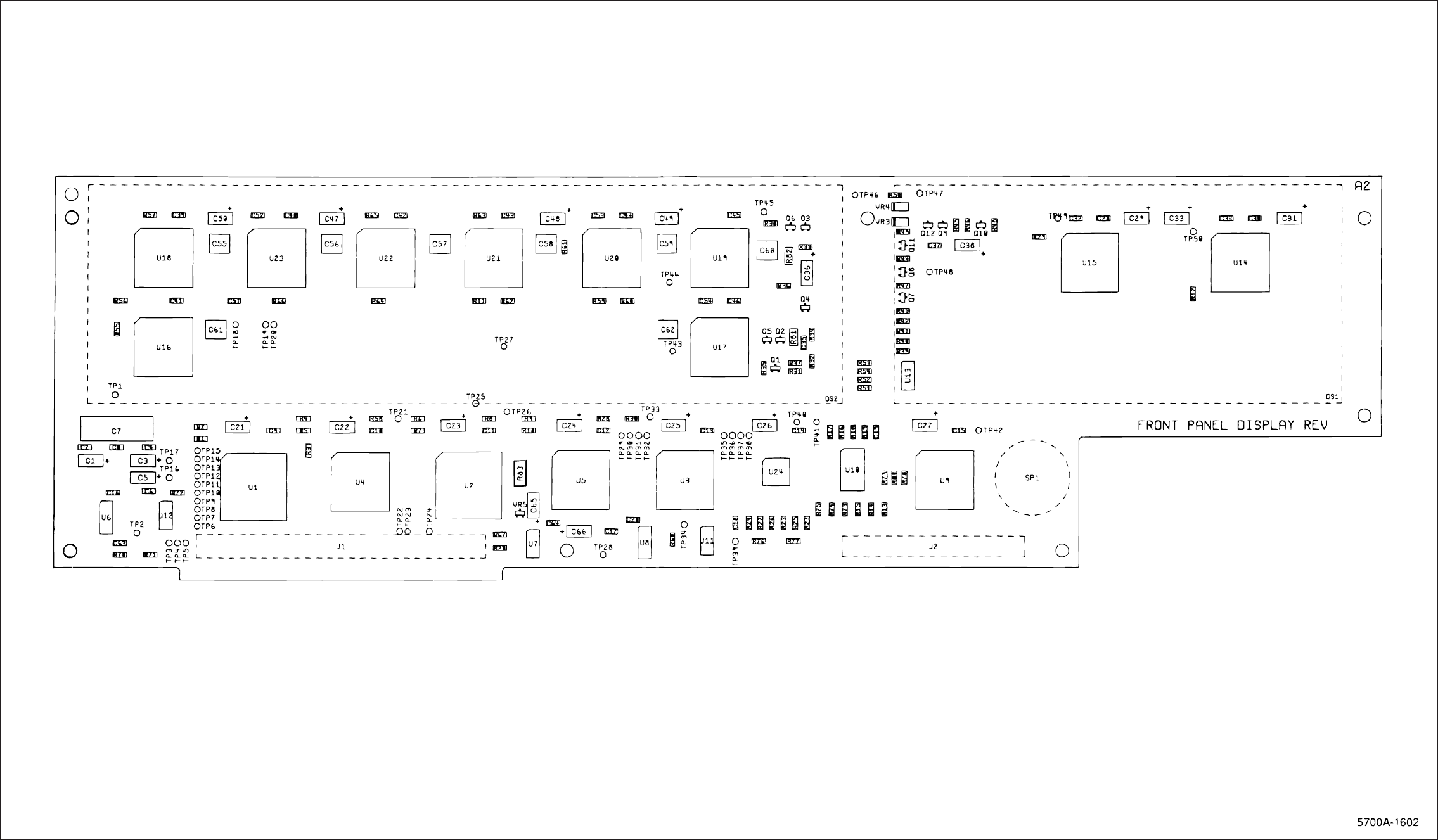
7
Schematic Diagrams
7-5
Figure 7-2. A2 Front Panel (PCA)
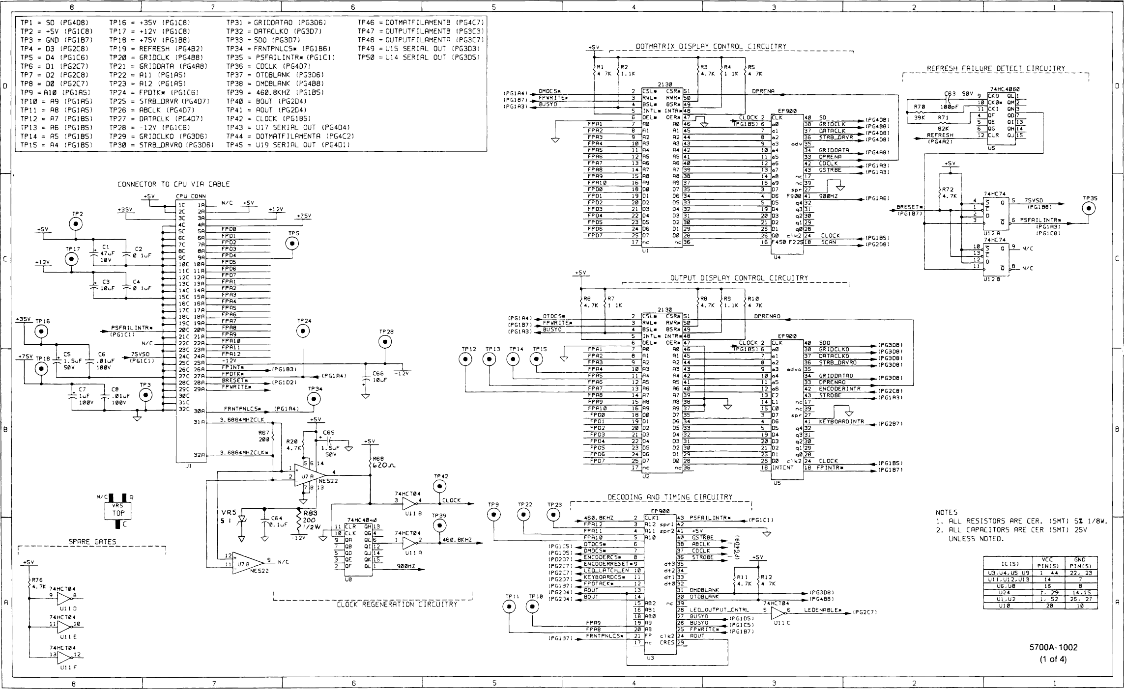
5700A/5720A Series II
Service Manual
7-6 Figure 7-2. A2 Front Panel PCA (cont)
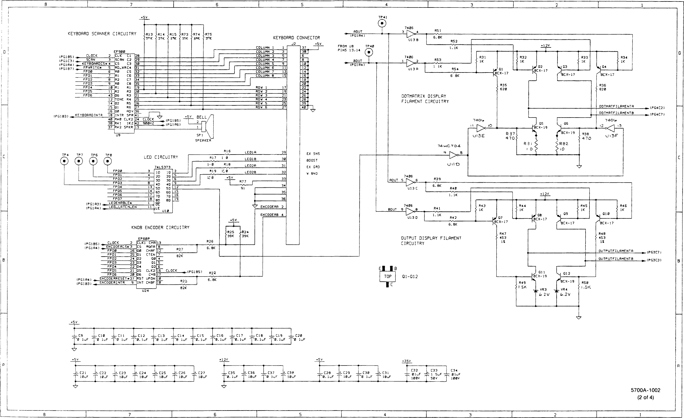
7
Schematic Diagrams
7-7
Figure 7-2. A2 Front Panel PCA (cont)
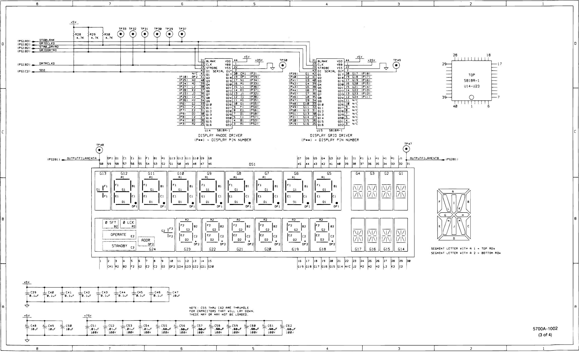
5700A/5720A Series II
Service Manual
7-8 Figure 7-2. A2 Front Panel PCA (cont)
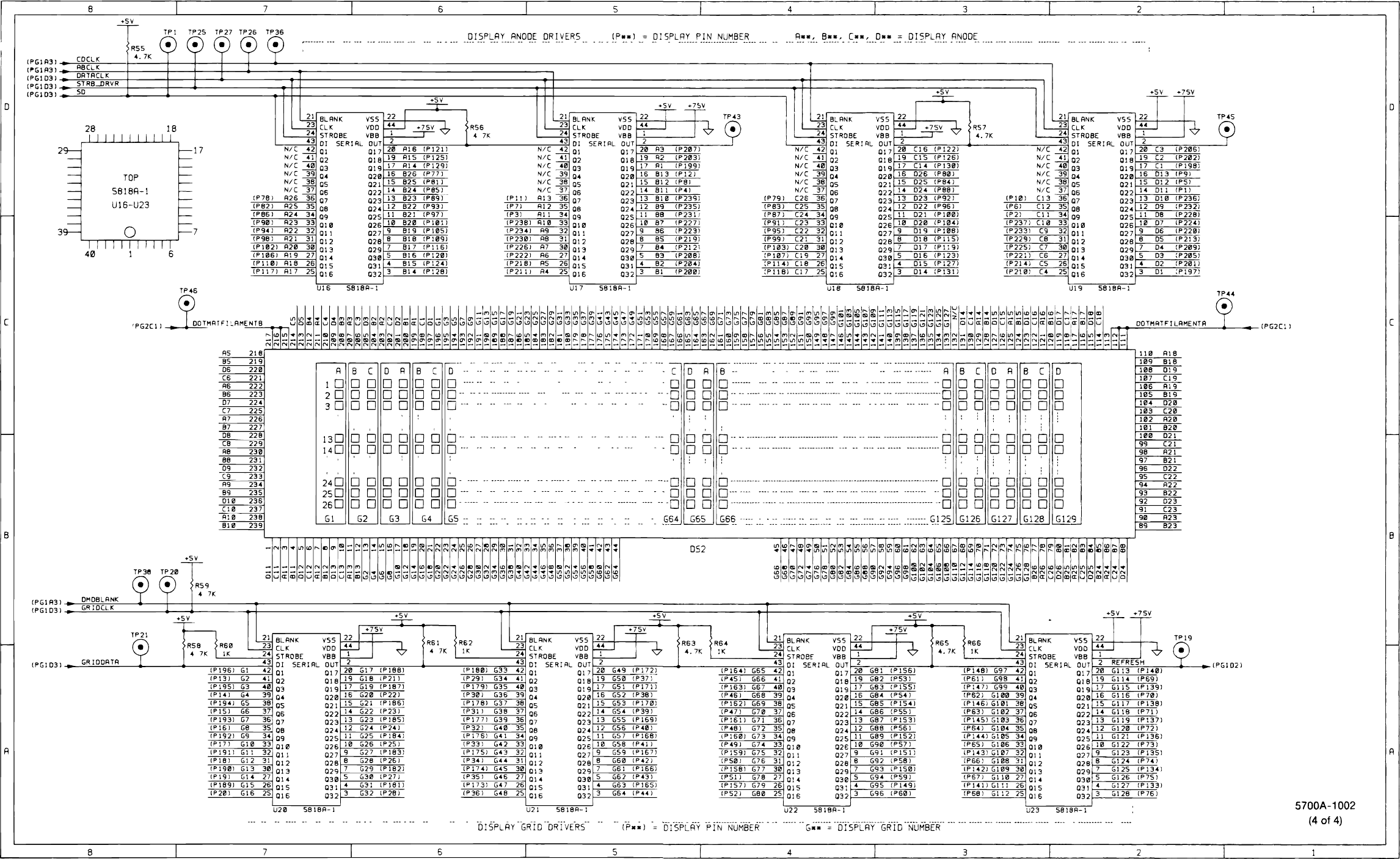
7
Schematic Diagrams
7-9
Figure 7-2. A2 Front Panel PCA (cont)
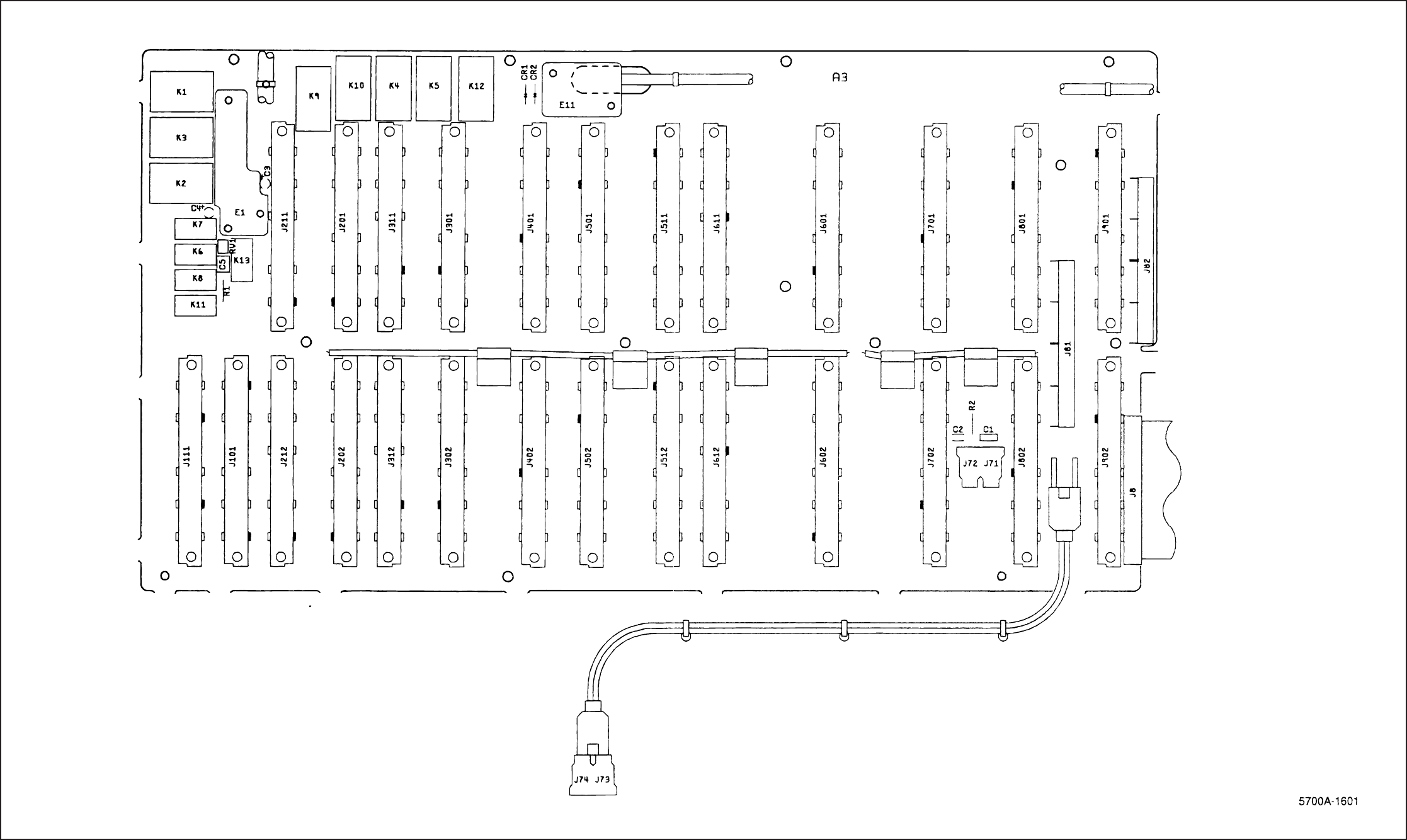
5700A/5720A Series II
Service Manual
7-10
Figure 7-3. A3 Analog Motherboard PCA
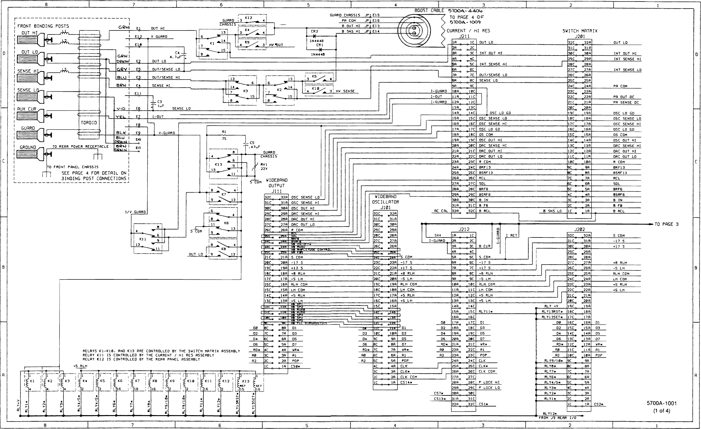
7
Schematic Diagrams
7-11
Figure 7-23. A3 Analog Motherboard PCA (cont)
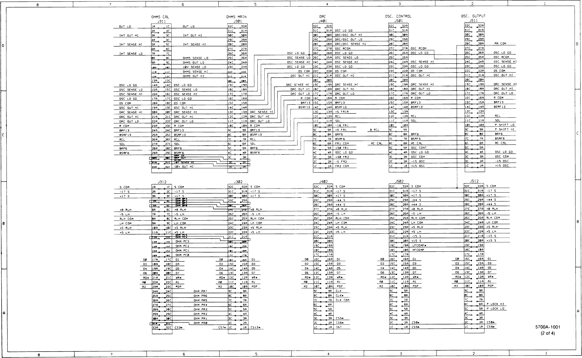
5700A/5720A Series II
Service Manual
7-12 Figure 7-3. A3 Analog Motherboard PCA (cont)
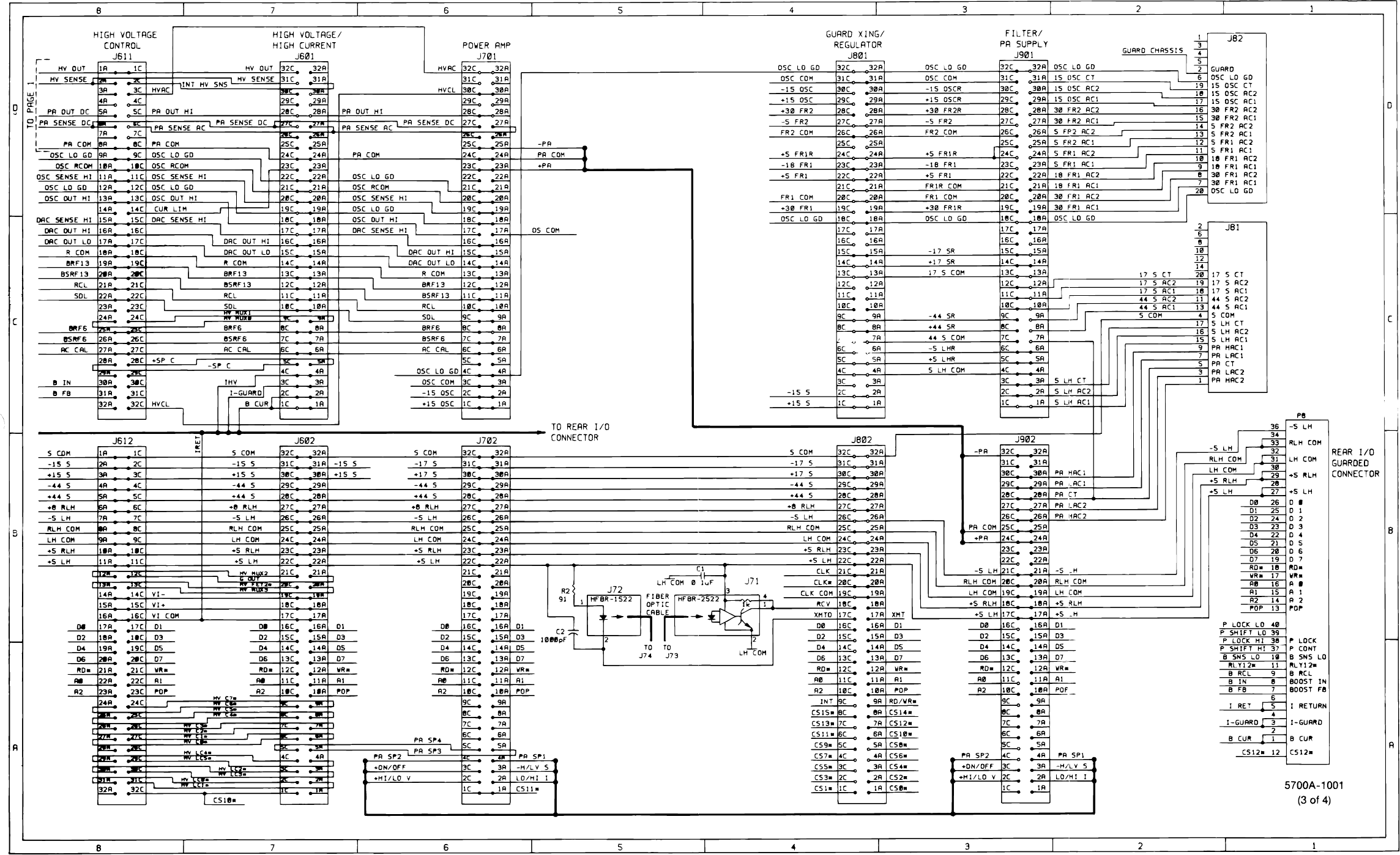
7
Schematic Diagrams
7-13
Figure 7-3. A3 Analog Motherboard PCA (cont)
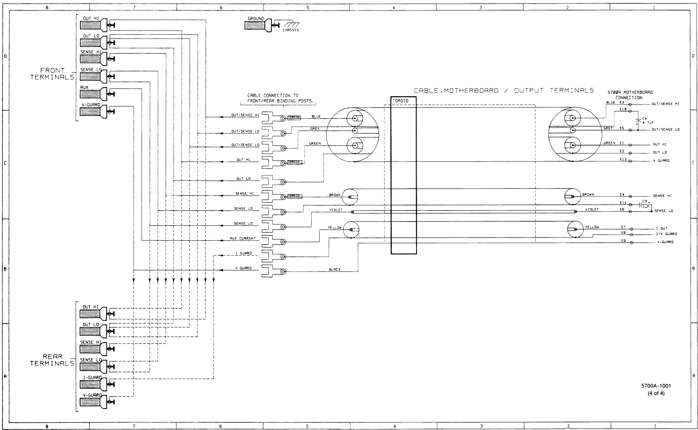
5700A/5720A Series II
Service Manual
7-14 Figure 7-3. A3 Analog Motherboard PCA (cont)
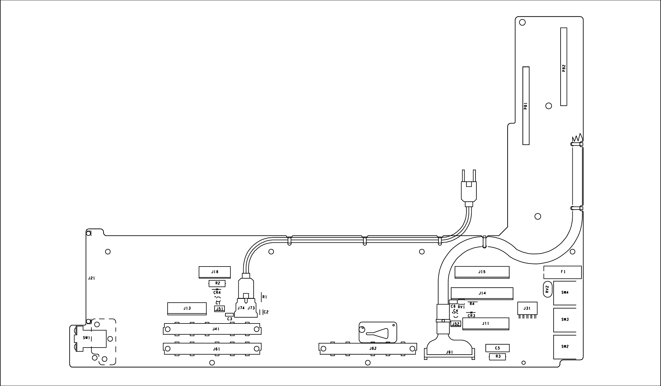
7
Schematic Diagrams
7-15
5700A-1605
Figure 7-4. A4 Digital Motherboard PCA
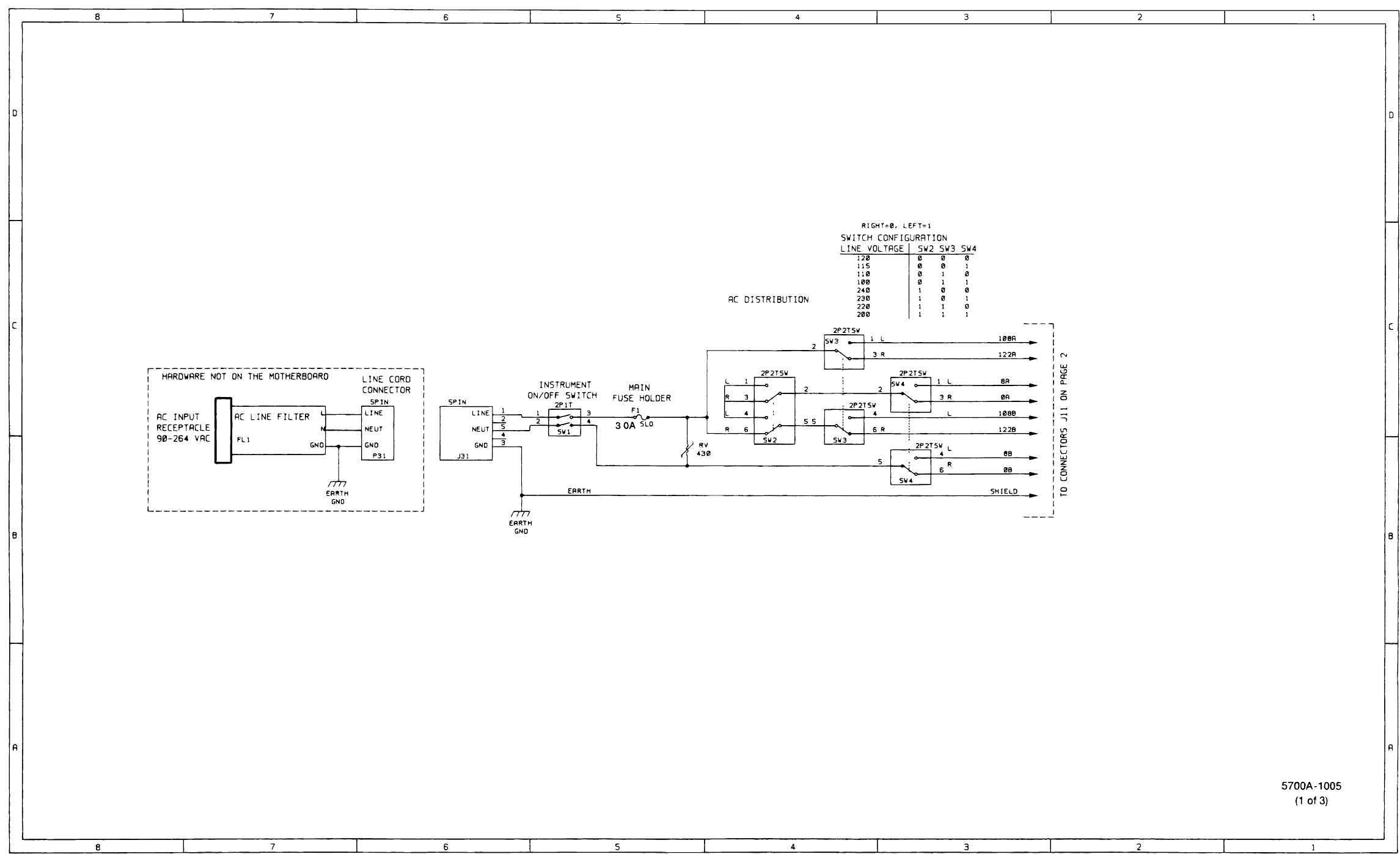
5700A/5720A Series II
Service Manual
7-16 Figure 7-4. A4 Digital Motherboard PCA (cont)
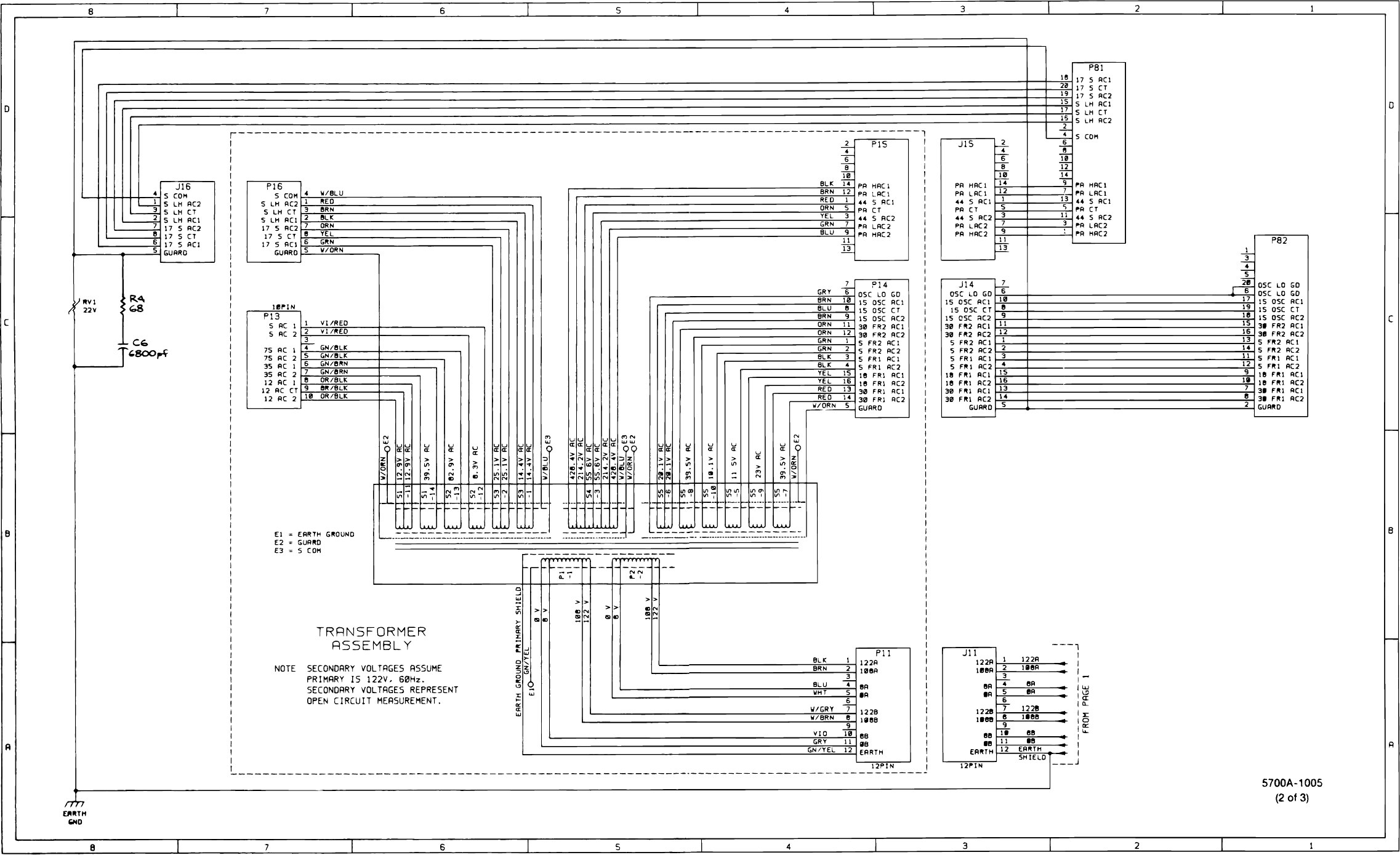
7
Schematic Diagrams
7-17
ahp46f.tif
Figure 7-4. A4 Digital Motherboard PCA (cont)
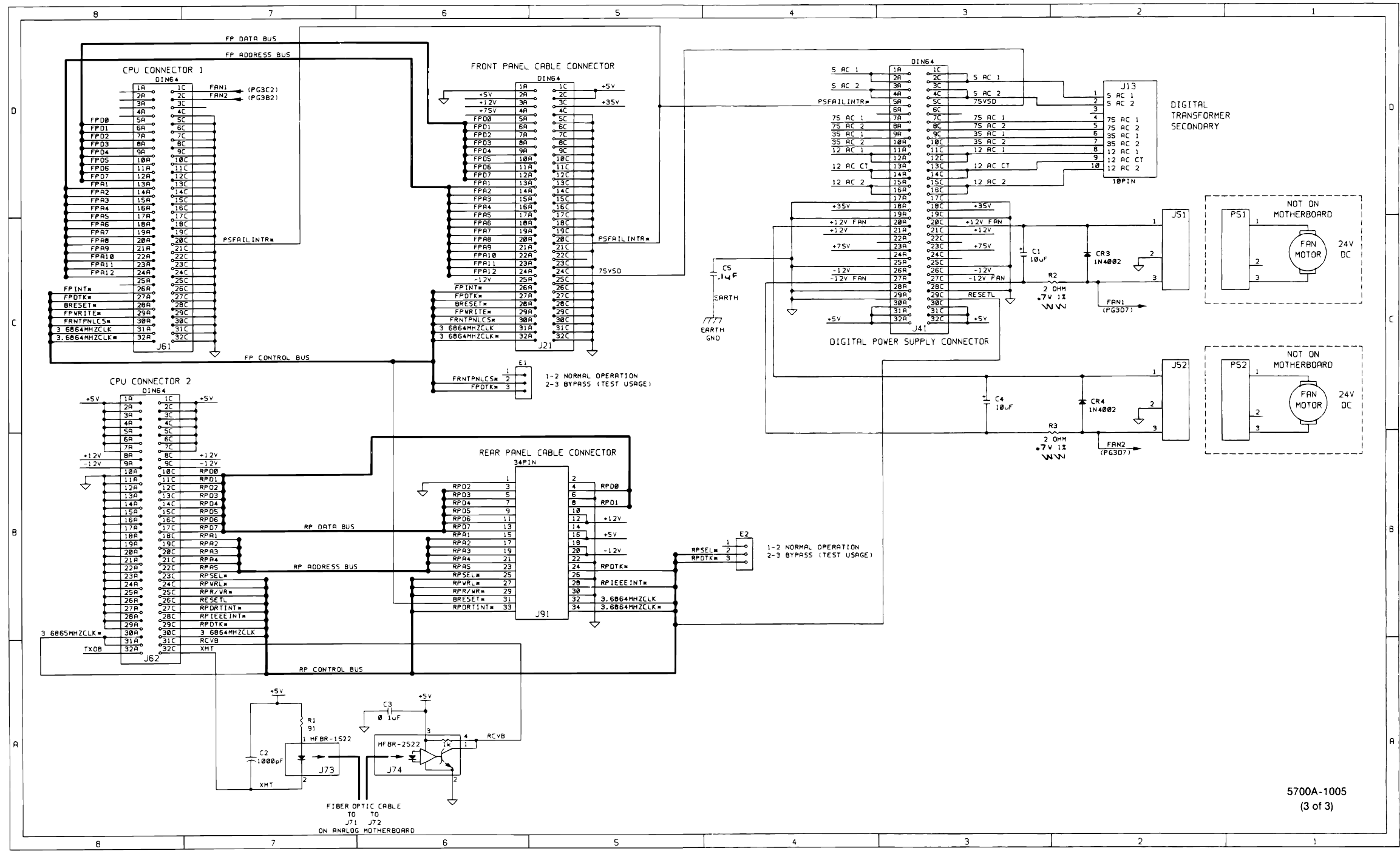
5700A/5720A Series II
Service Manual
7-18 Figure 7-4. A4 Digital Motherboard PCA (cont)
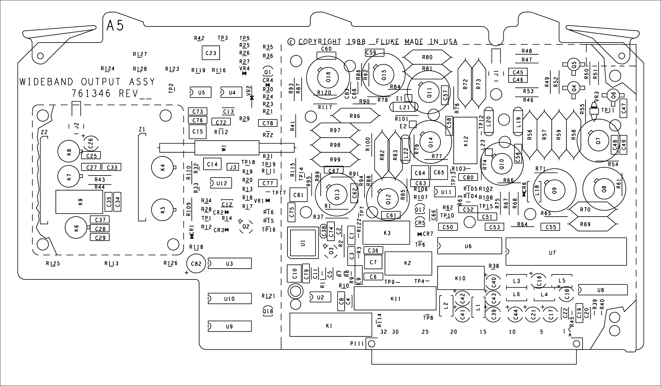
7
Schematic Diagrams
7-19
5700A-1611
Figure 7-5. A5 Wideband Output PCA (Option -03)
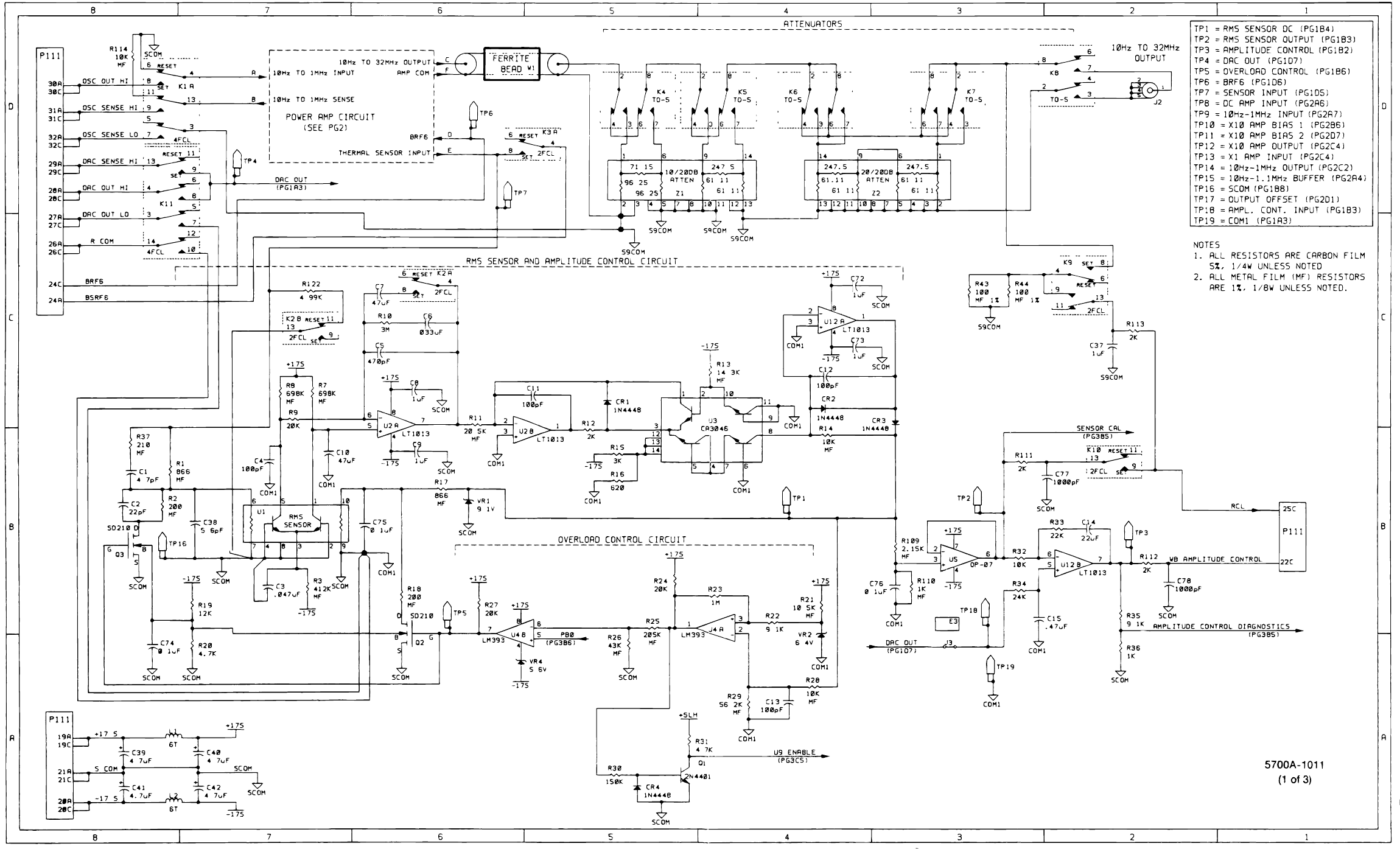
5700A/5720A Series II
Service Manual
7-20
Figure 7-5. A5 Wideband Output PCA (Option -03) (cont)
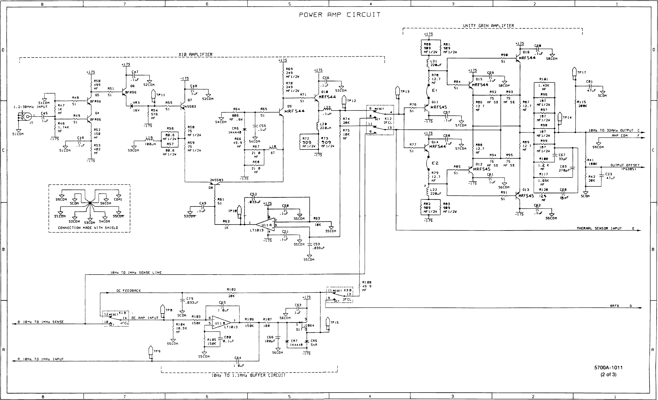
7
Schematic Diagrams
7-21
Figure 7-5. A5 Wideband Output PCA (Option -03) (cont)
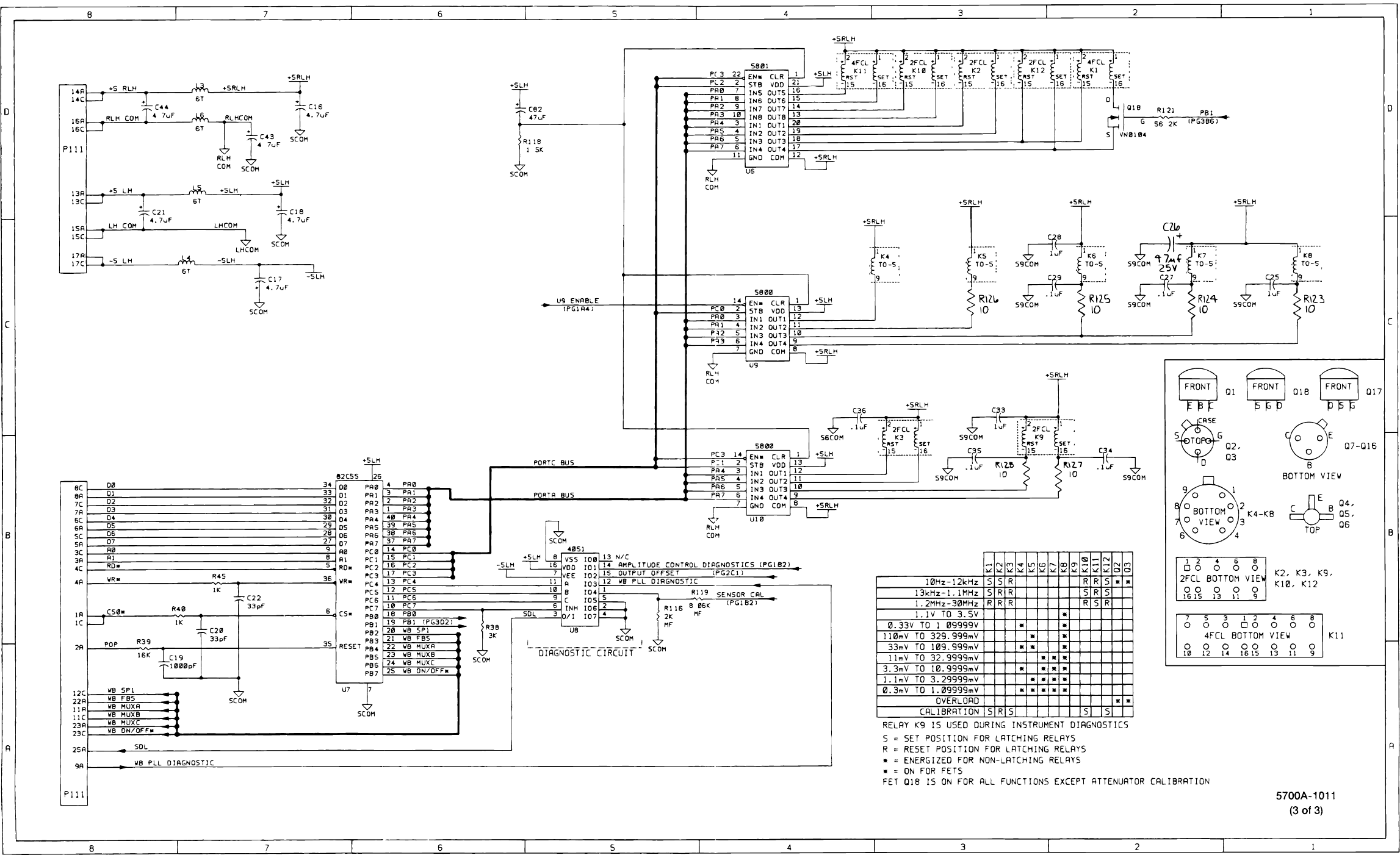
5700A/5720A Series II
Service Manual
7-22 Figure 7-5. A5 Wideband Output PCA (Option -03) (cont)
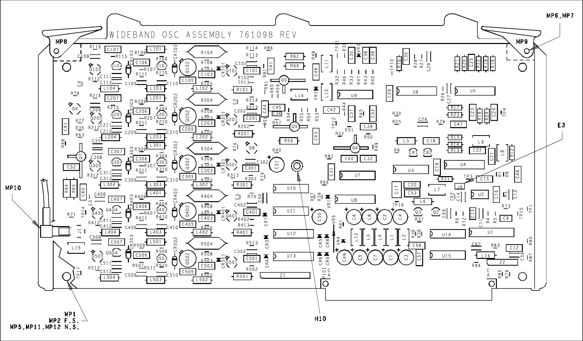
7
Schematic Diagrams
7-23
5700A-7610
Figure 7-6. A6 Wideband Oscillator PCA (Option -03)
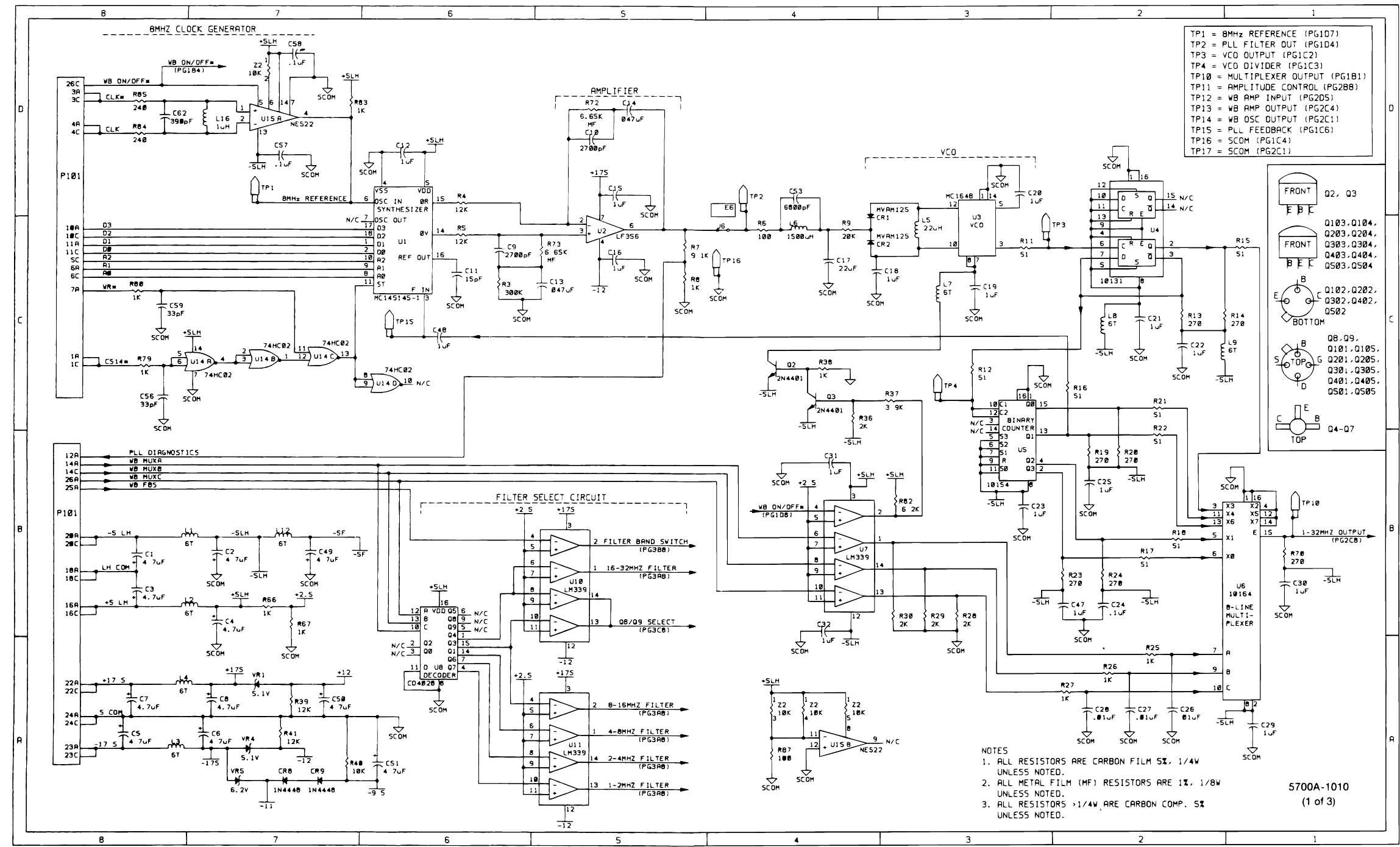
5700A/5720A Series II
Service Manual
7-24
Figure 7-6. A6 Wideband Output PCA (Option -03)
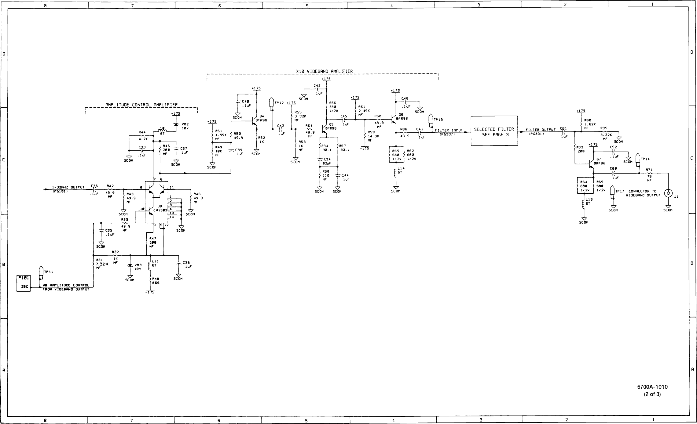
7
Schematic Diagrams
7-25
Figure 7-6. A6 Wideband Oscillator PCA (Option -03) (cont)
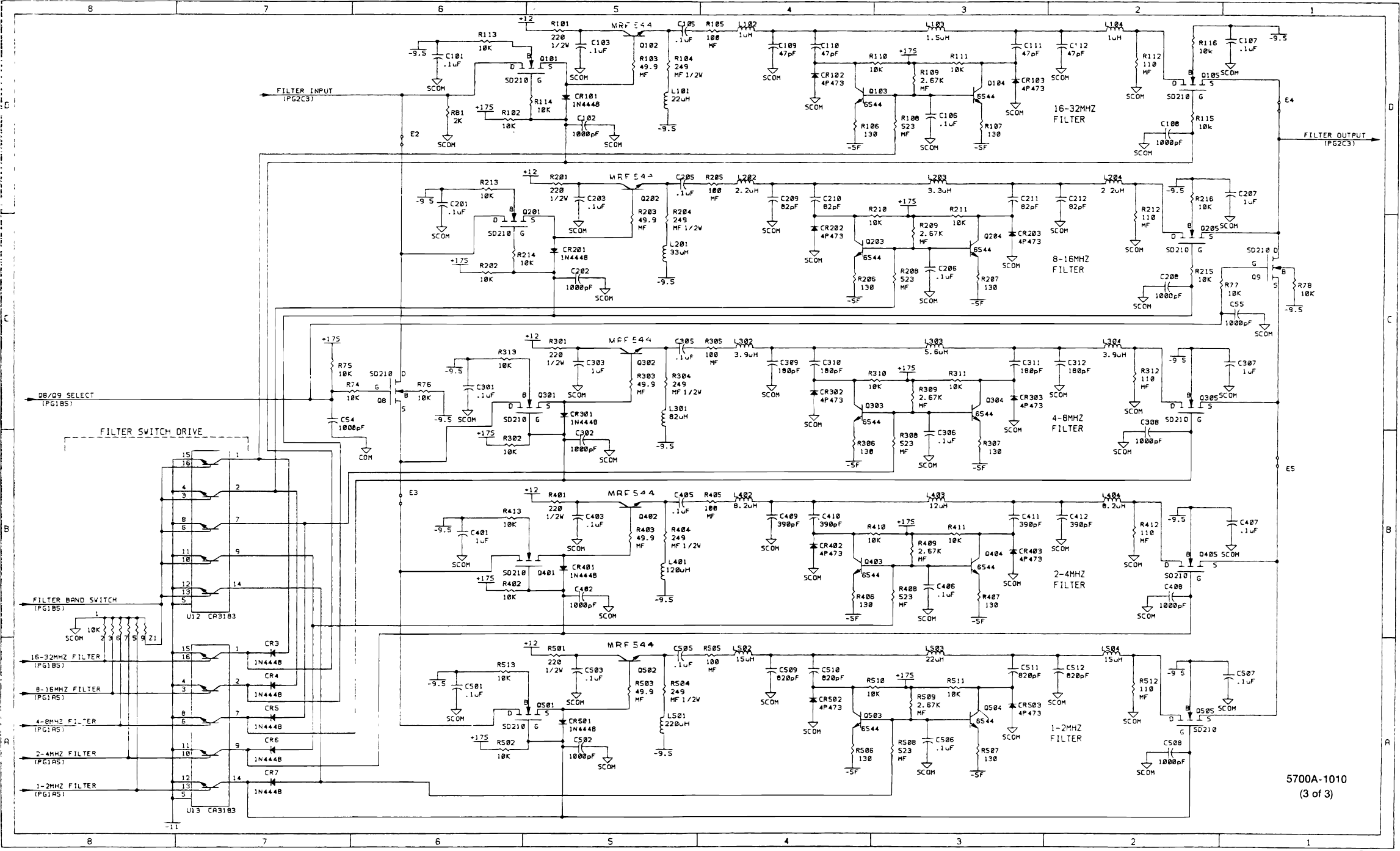
5700A/5720A Series II
Service Manual
7-26
Figure 7-6. A6 Wideband Oscillator PCA (Option -03) (cont)
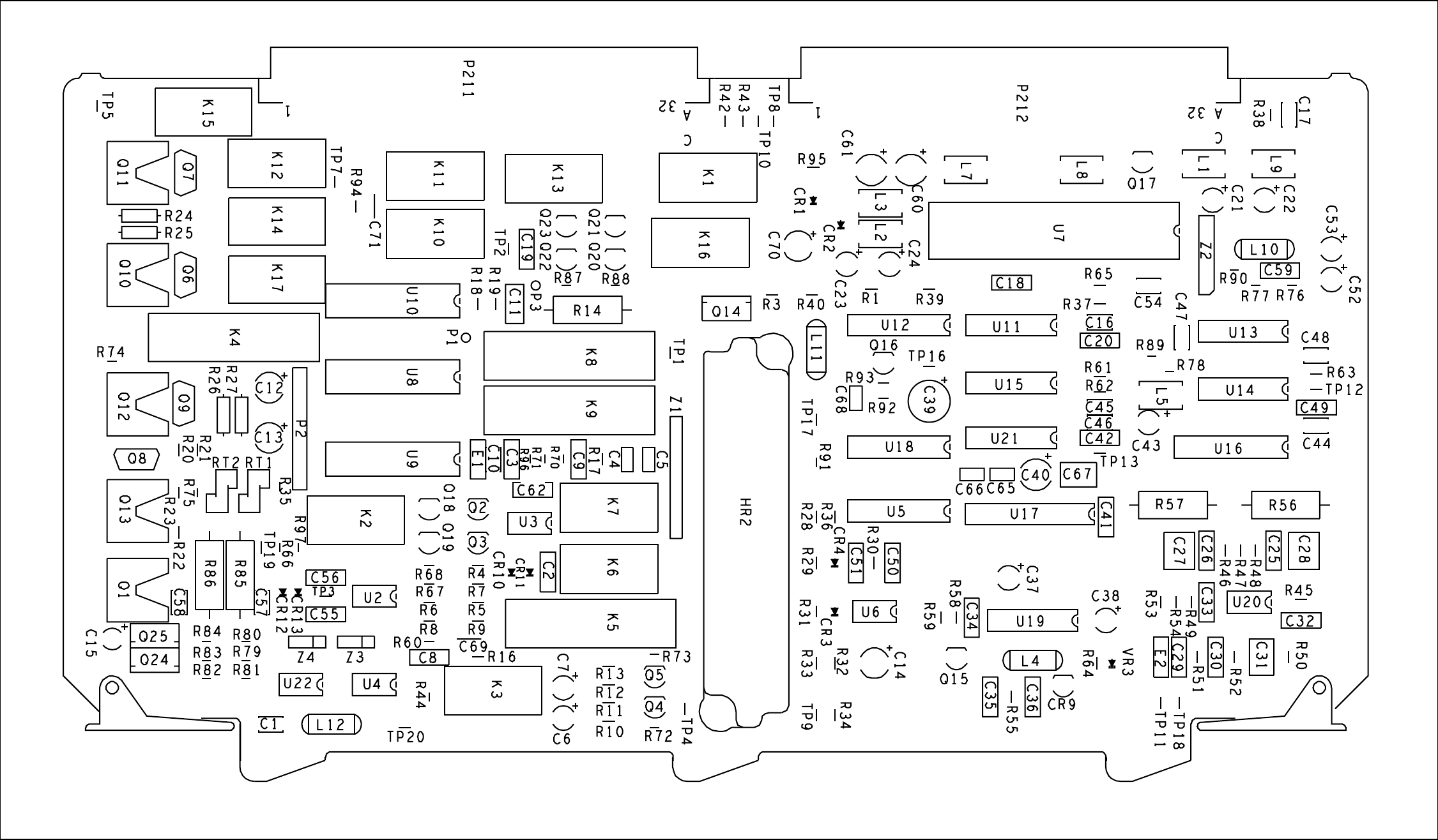
7
Schematic Diagrams
7-27
5700A-1621
Figure 7-7. A7 Current/High-Resolution Oscillator PCA
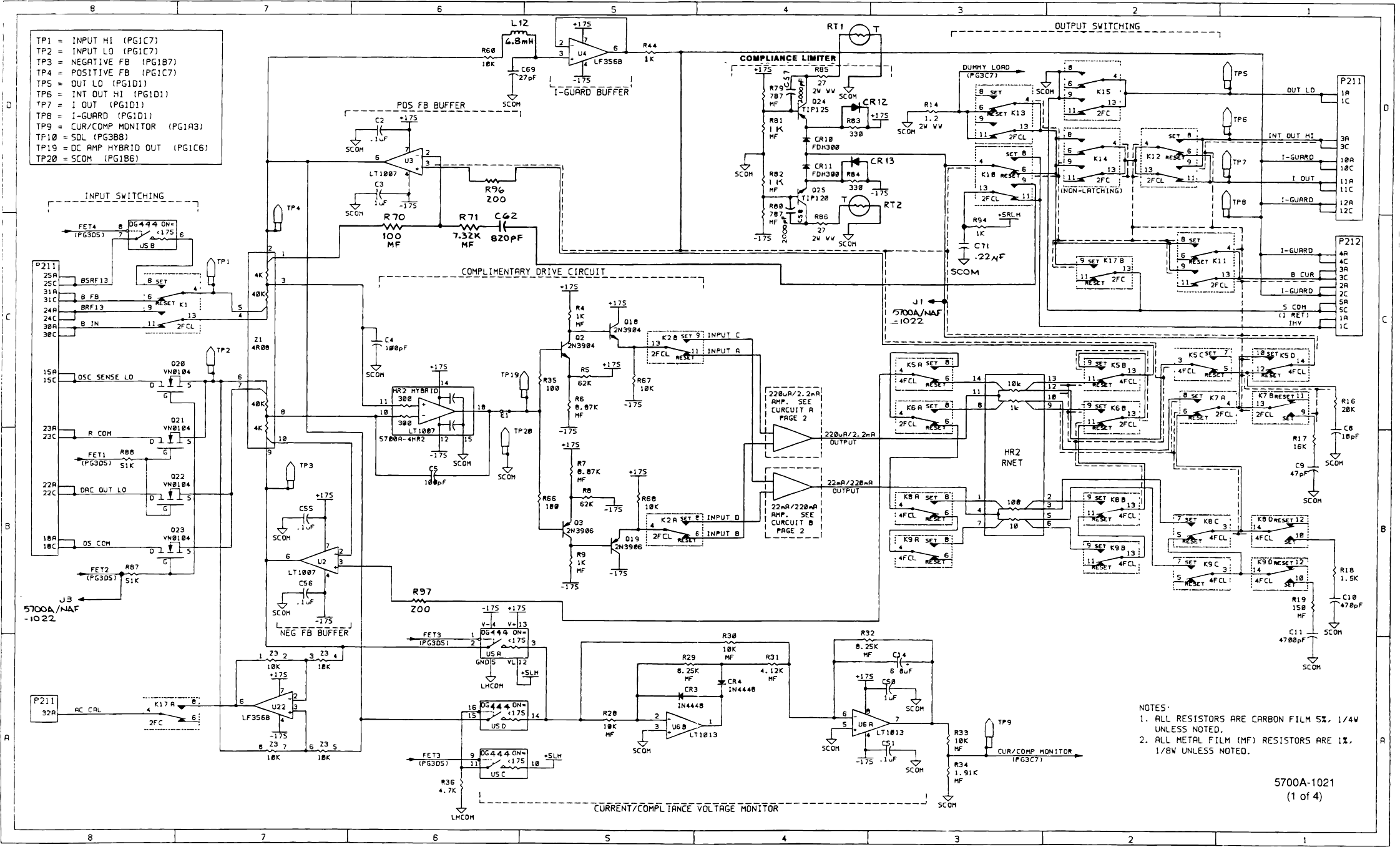
5700A/5720A Series II
Service Manual
7-28
Figure 7-7. A7 Current/High-Resolution
Oscillator PCA (cont)
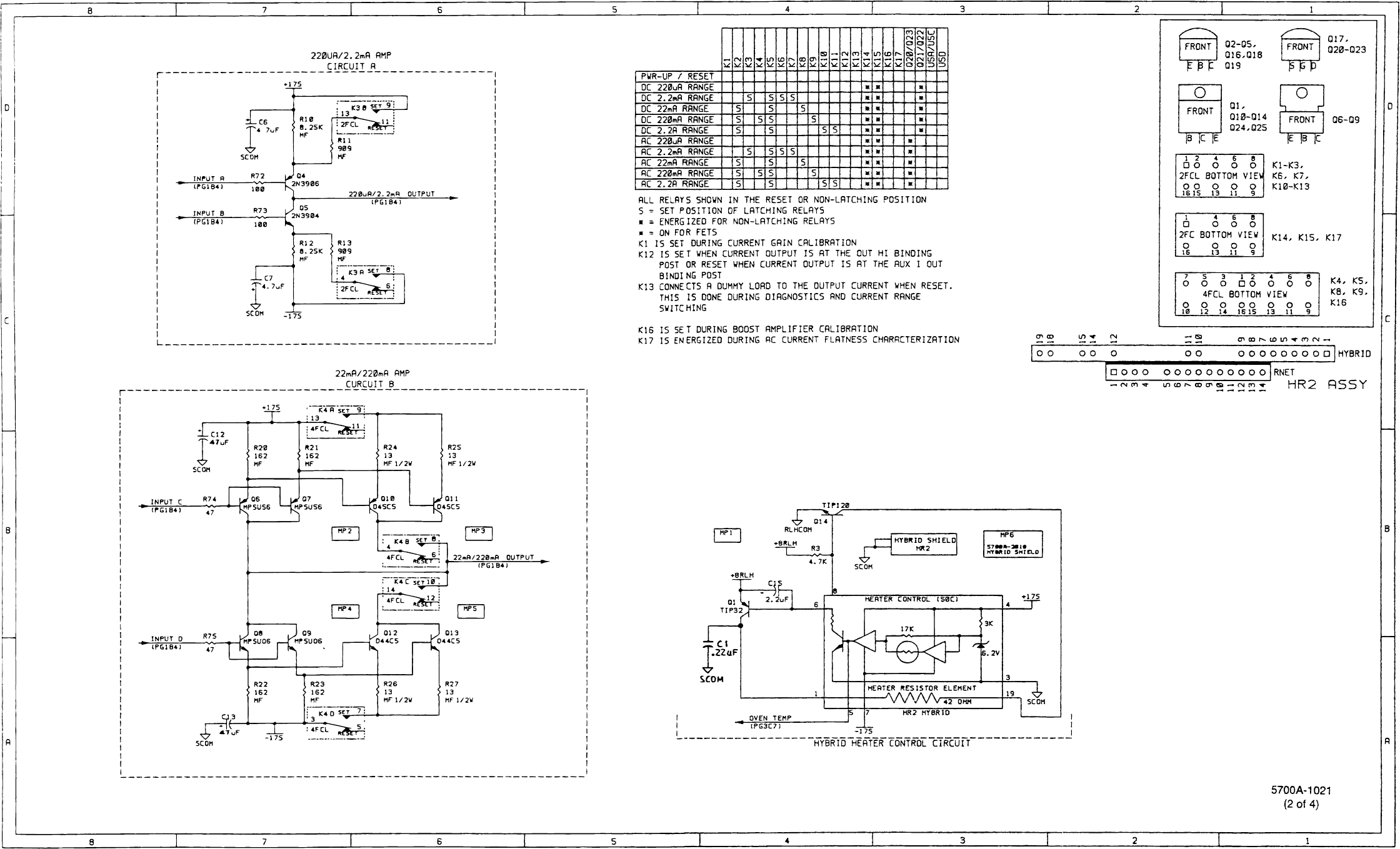
7
Schematic Diagrams
7-29
Figure 7-7. A7 Current/High-Resolution
Oscillator PCA (cont)

5700A/5720A Series II
Service Manual
7-30
Figure 7-7. A7 Current/High-Resolution Oscillator PCA (cont)
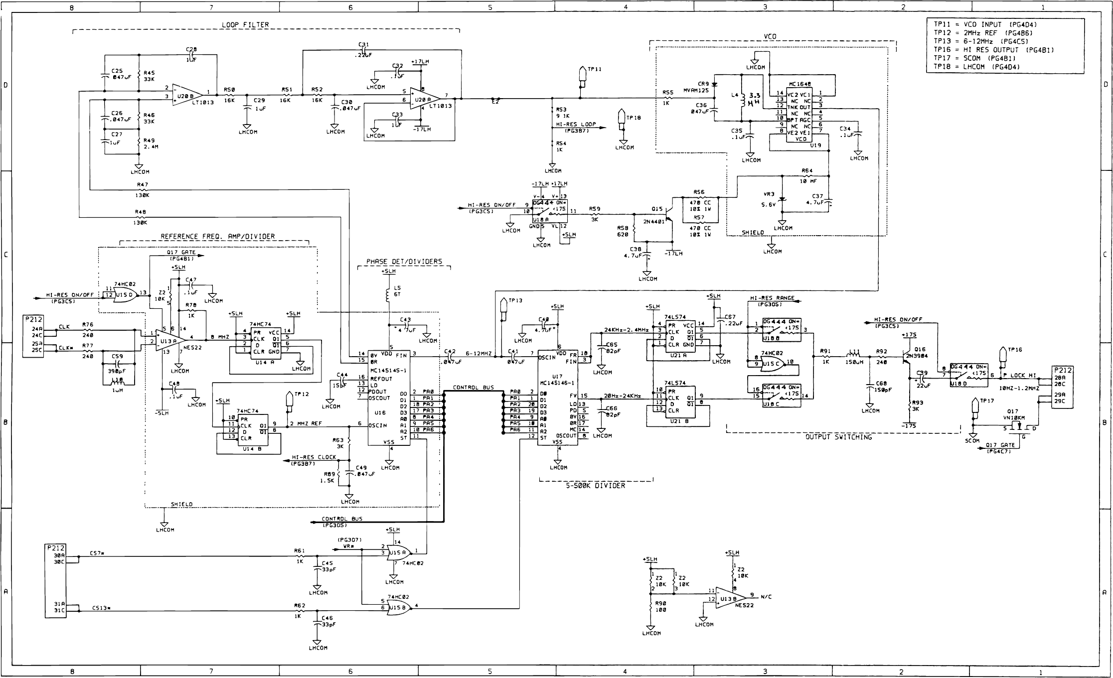
7
Schematic Diagrams
7-31
Figure 7-7. A7 Current/High-Resolution
Oscillator PCA (cont)
5700A-1021
(4 of 4)
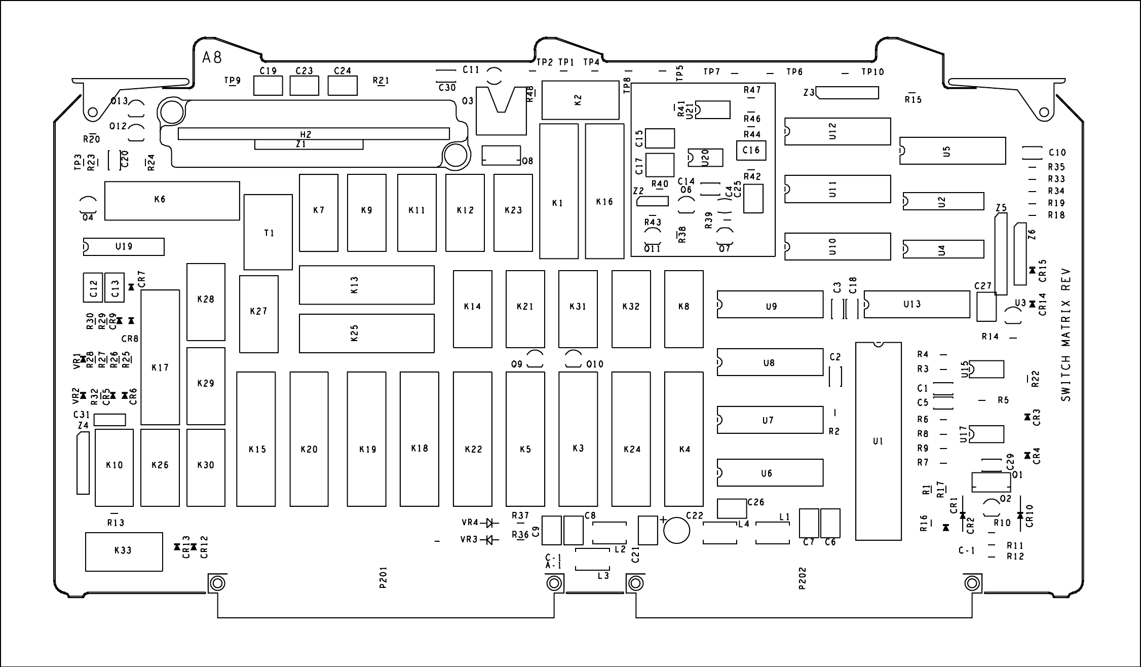
5700A/5720A Series II
Service Manual
7-32
5700A-1622
Figure 7-8. A8 Switch Matrix PCA
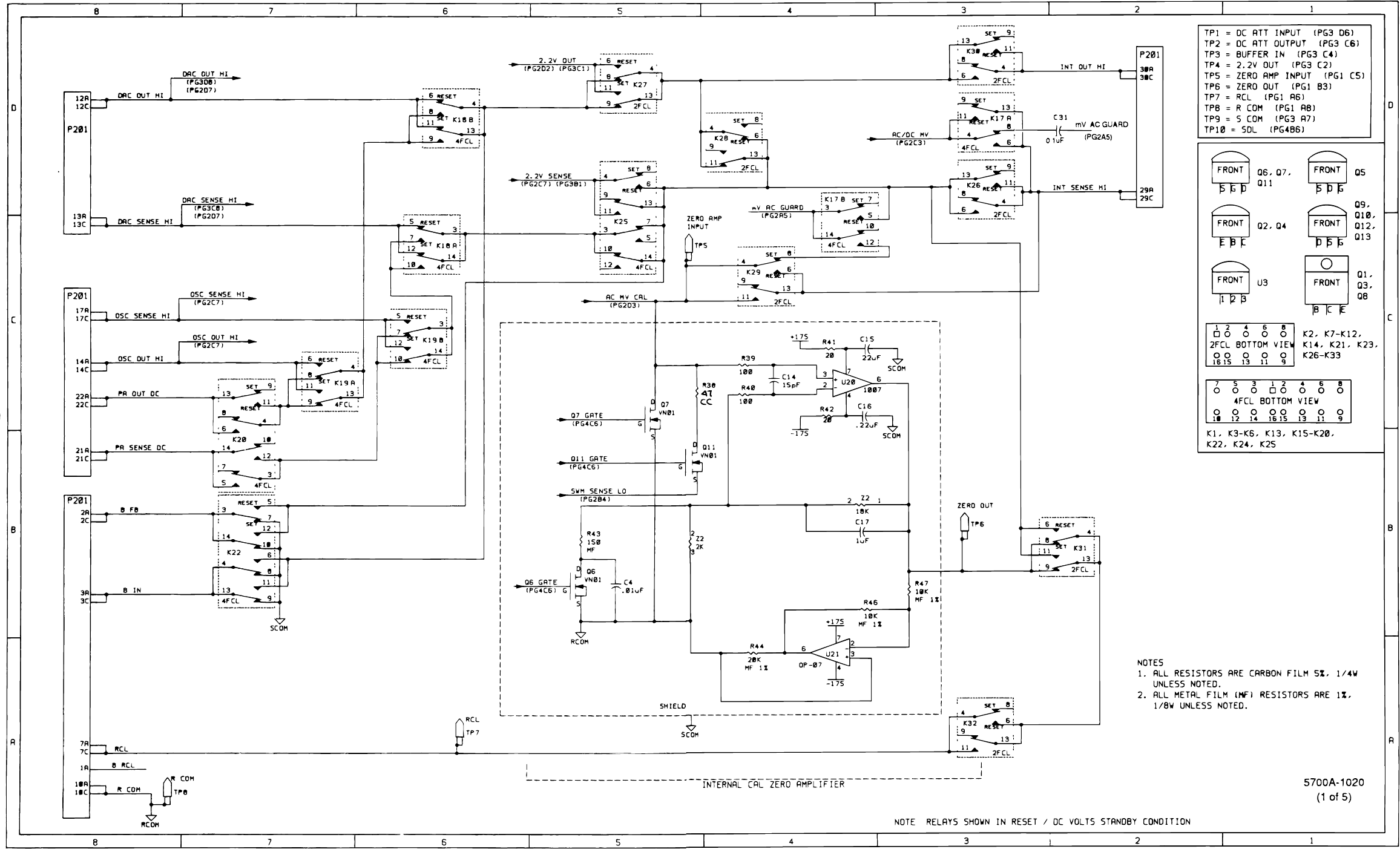
7
Schematic Diagrams
7-33
Figure 7-8. A8 Swith Matrix PCA (cont)
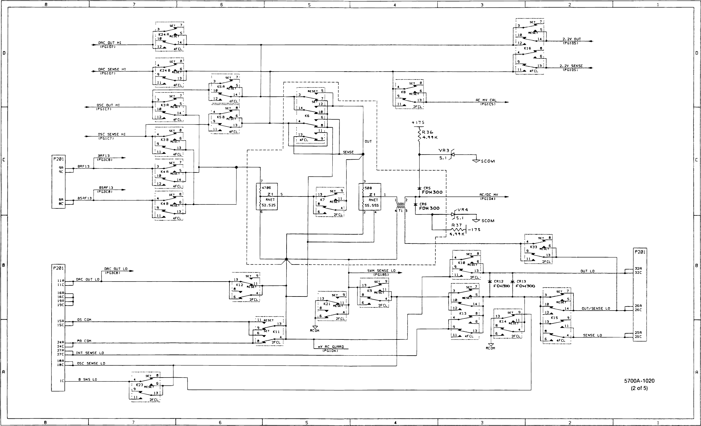
5700A/5720A Series II
Service Manual
7-34 Figure 7-8. A8 Switch Matrix PCA (cont)

7
Schematic Diagrams
7-35
Figure 7-8. A8 Swith Matrix PCA (cont)
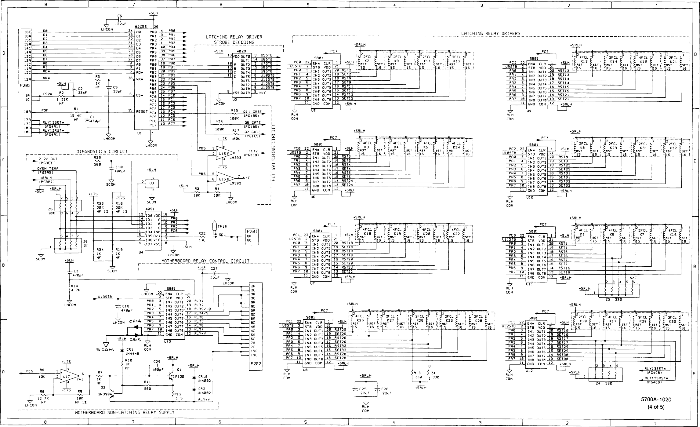
5700A/5720A Series II
Service Manual
7-36 Figure 7-8. A8 Switch Matrix PCA (cont)
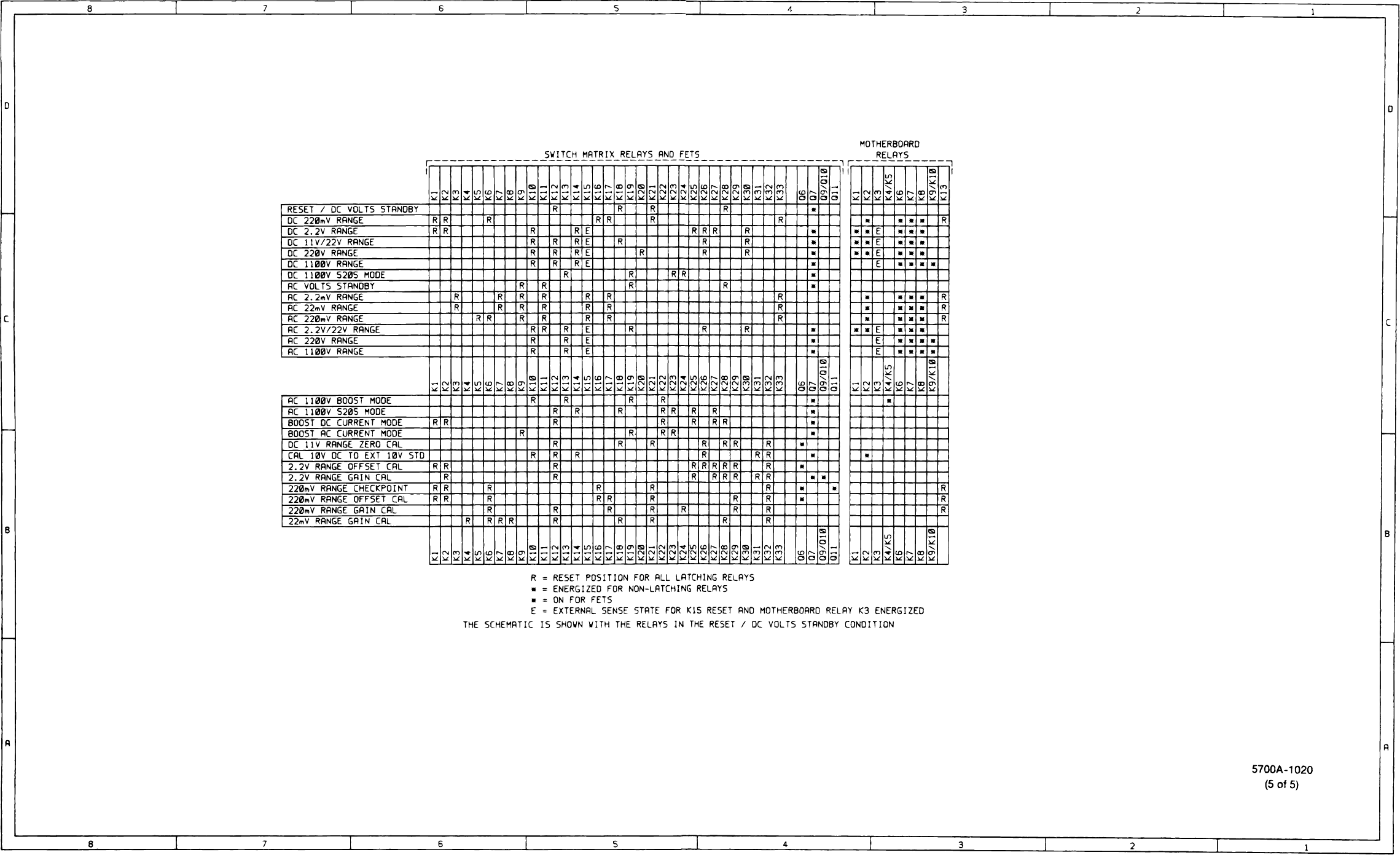
7
Schematic Diagrams
7-37
Figure 7-8. A8 Swith Matrix PCA (cont)
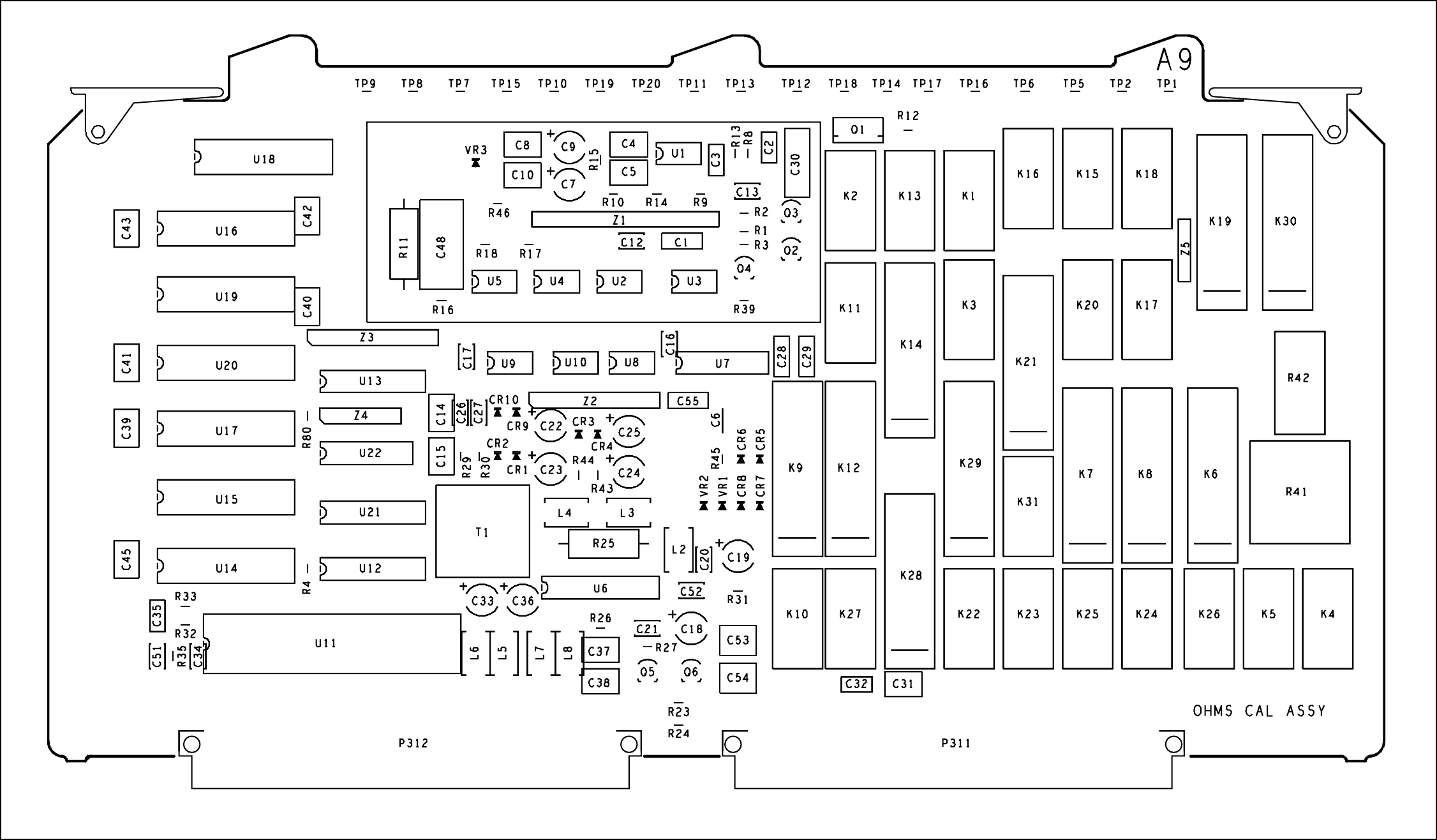
5700A/5720A Series II
Service Manual
7-38
5700A-1631
Figure 7-9. A9 Ohms Cal PCA
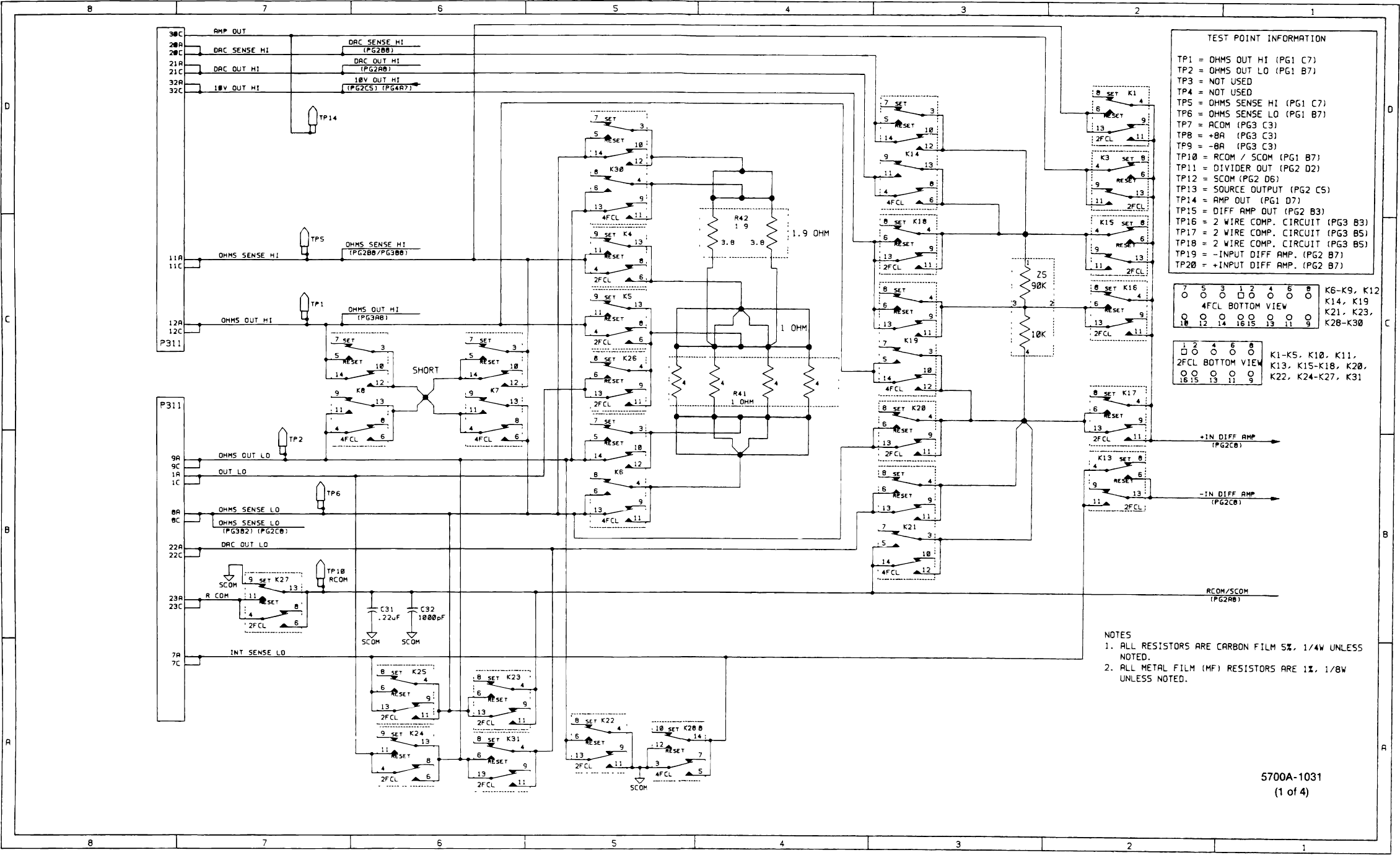
7
Schematic Diagrams
7-39
Figure 7-9. A9 Ohms Cal PCA (cont)
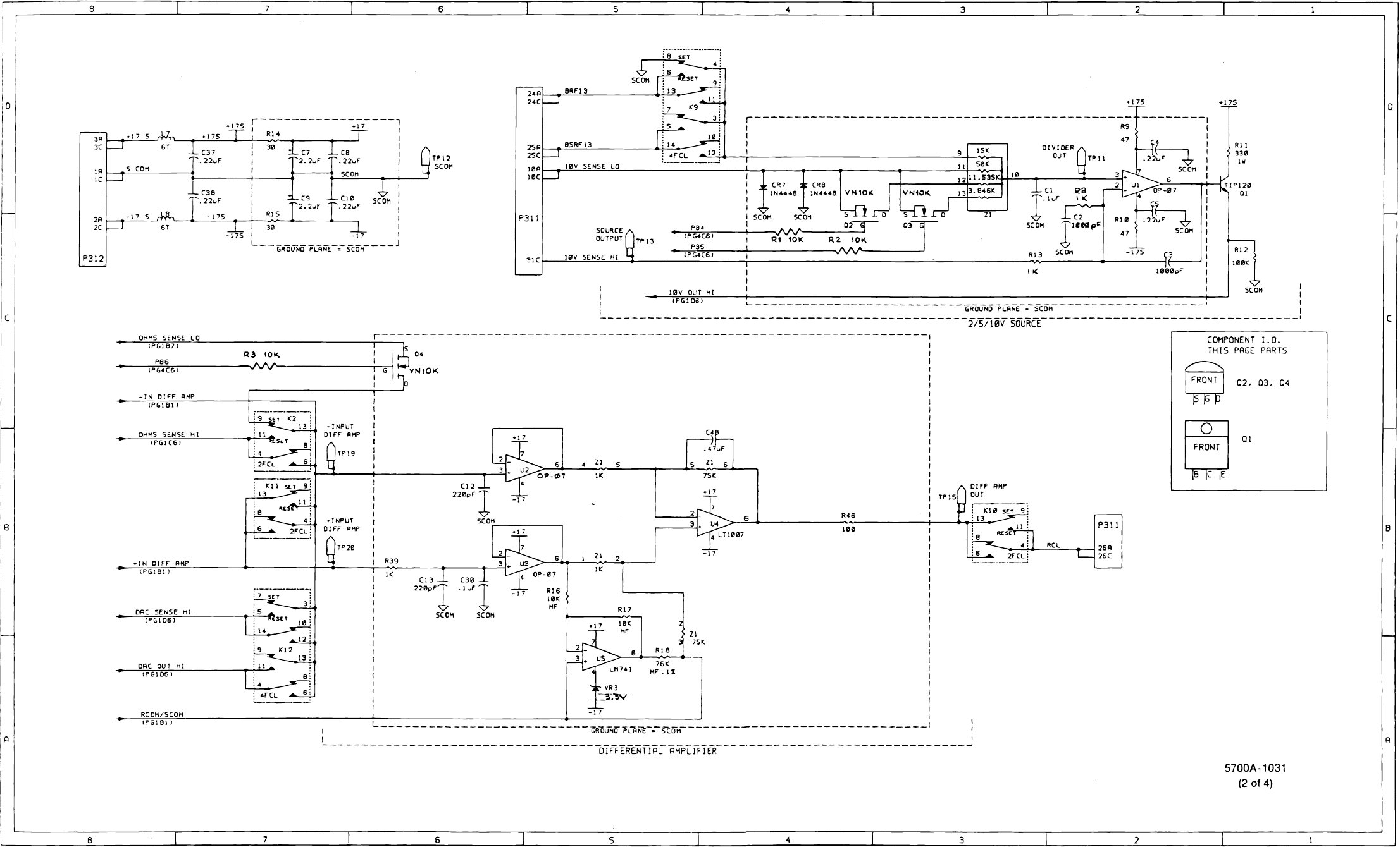
5700A/5720A Series II
Service Manual
7-40
Figure 7-9. A9 Ohms Cal PCA (cont)
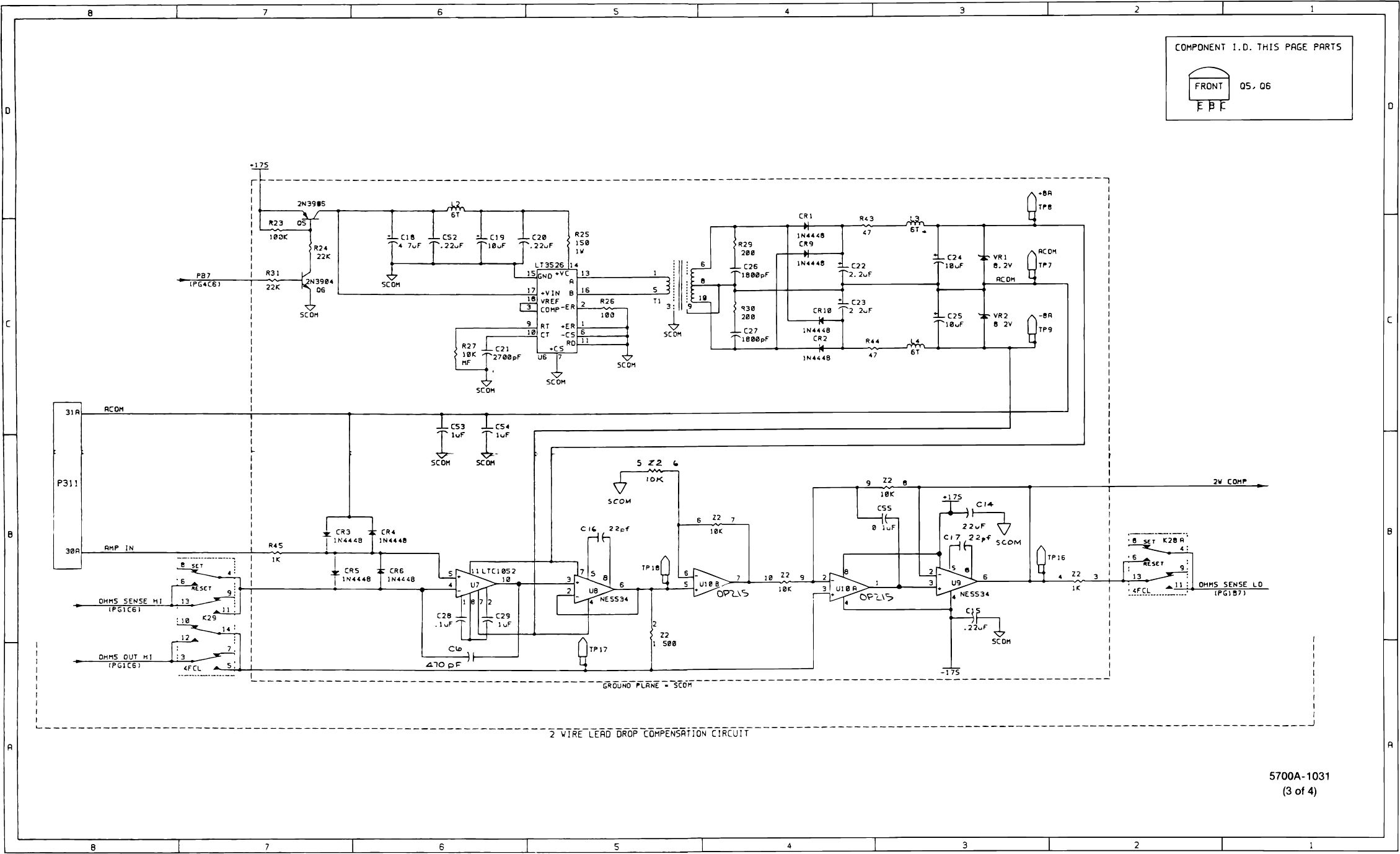
7
Schematic Diagrams
7-41
Figure 7-9. A9 Ohms Cal PCA (cont)
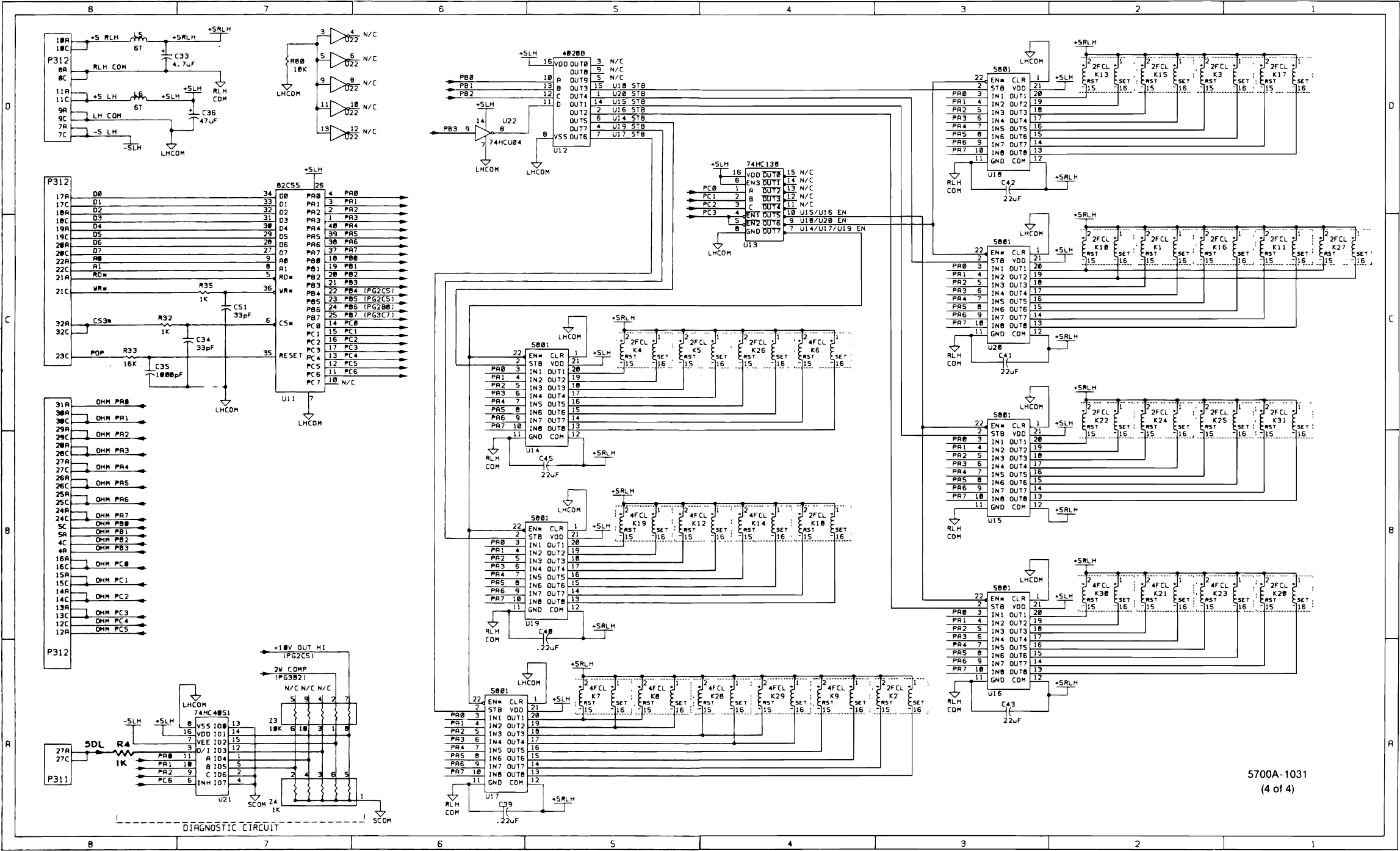
5700A/5720A Series II
Service Manual
7-42 Figure 7-9. A9 Ohms Cal PCA (cont)
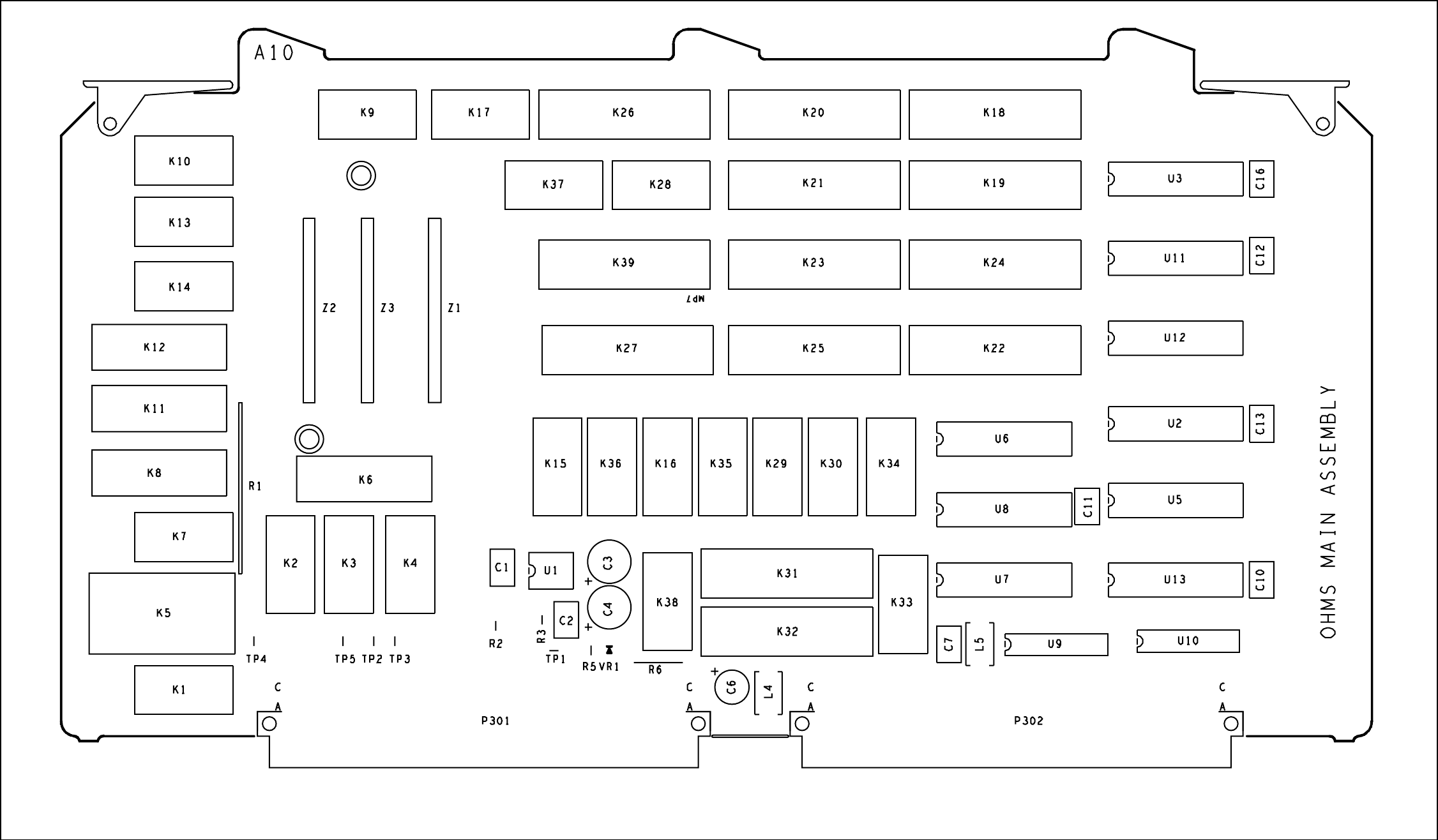
7
Schematic Diagrams
7-43
5700A-1630
Figure 7-10. A10 Ohms Main PCA
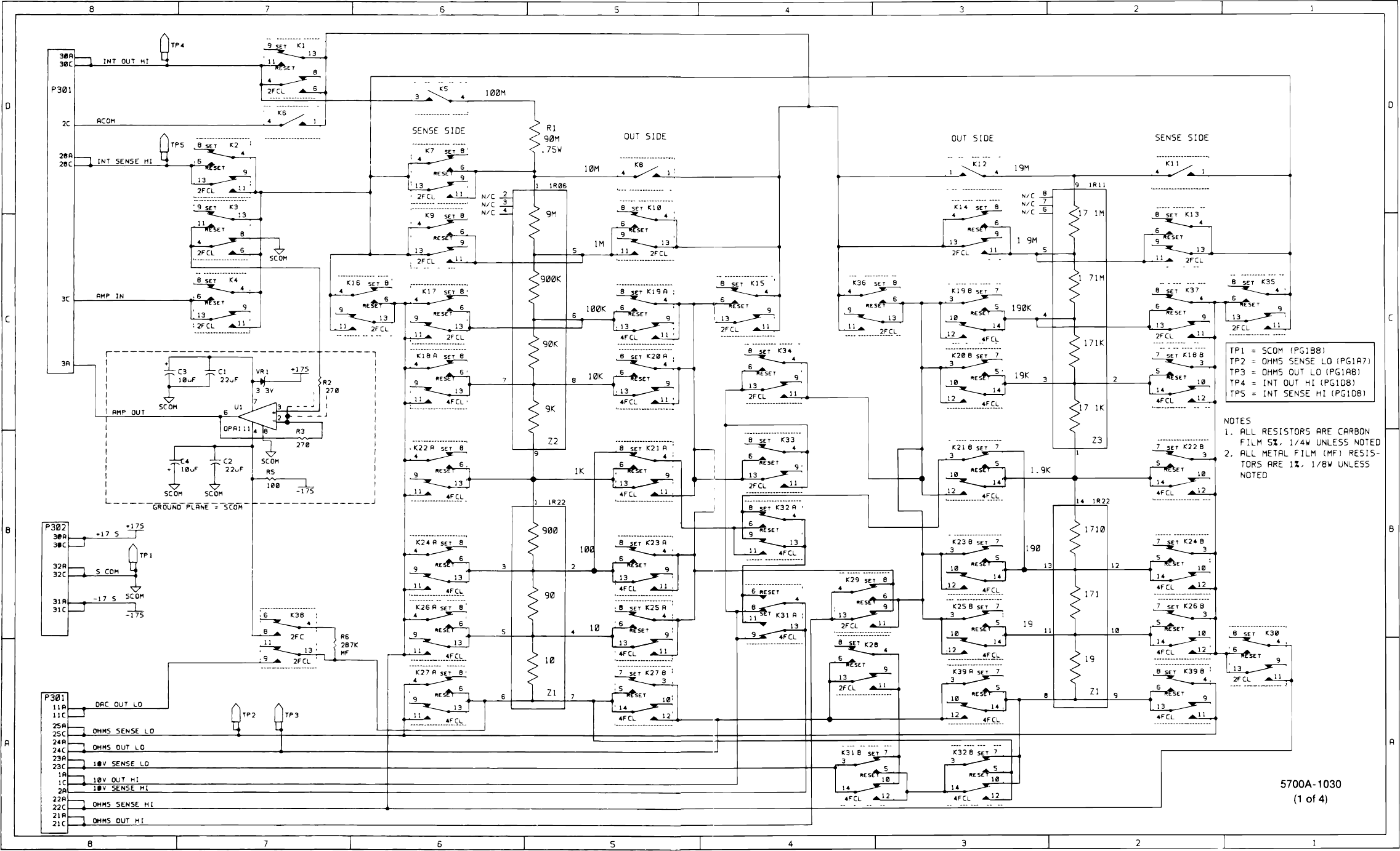
5700A/5720A Series II
Service Manual
7-44
Figure 7-10. A10 Ohms Main PCA (cont)
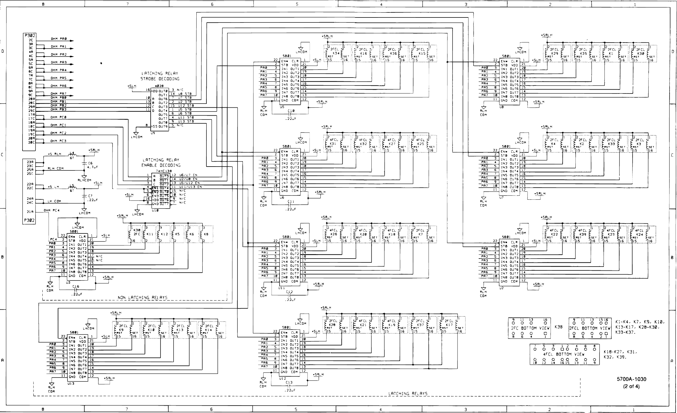
7
Schematic Diagrams
7-45
Figure 7-10. A10 Ohms Main PCA
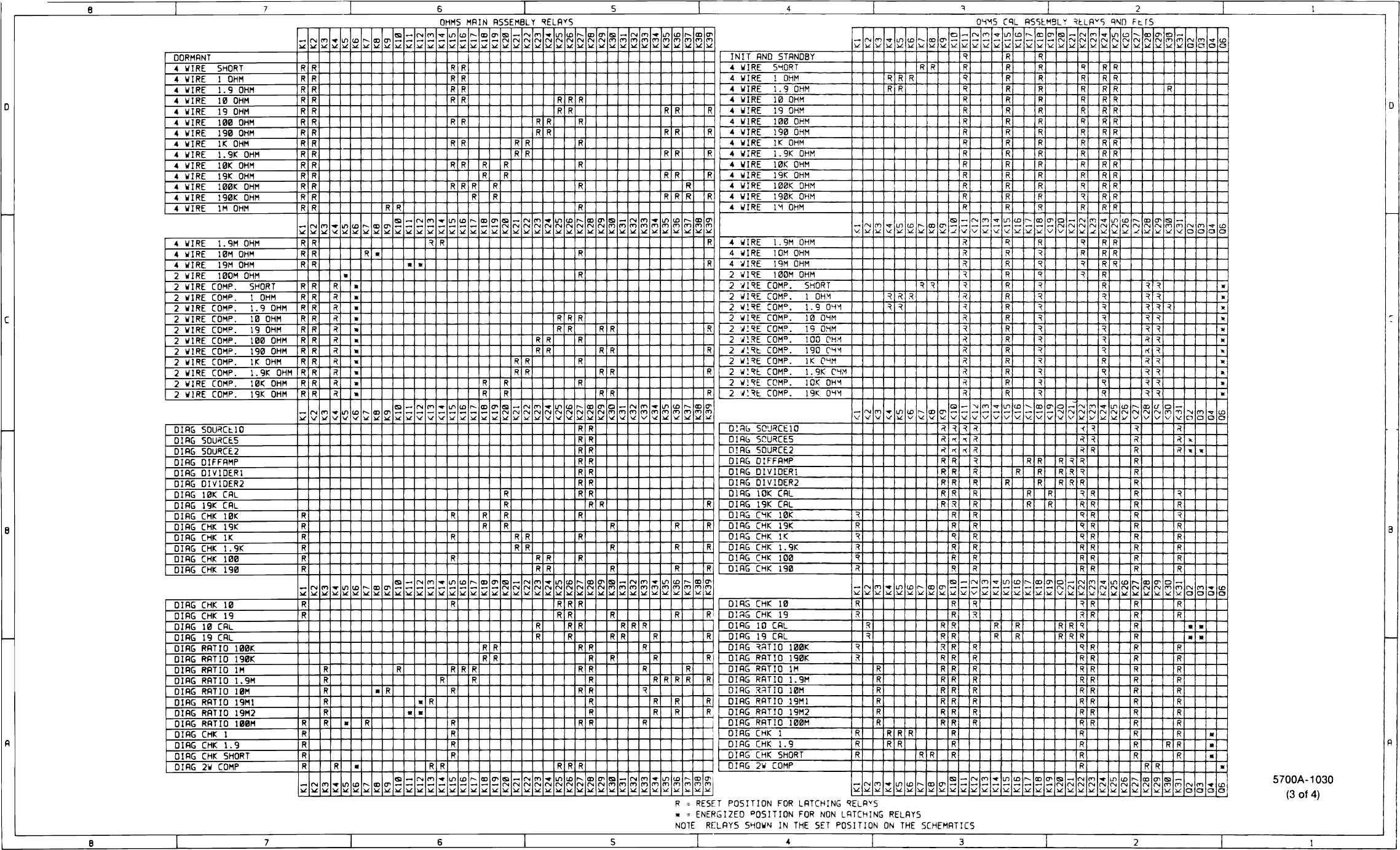
5700A/5720A Series II
Service Manual
7-46
Figure 7-10. A10 Ohms Main PCA (cont)
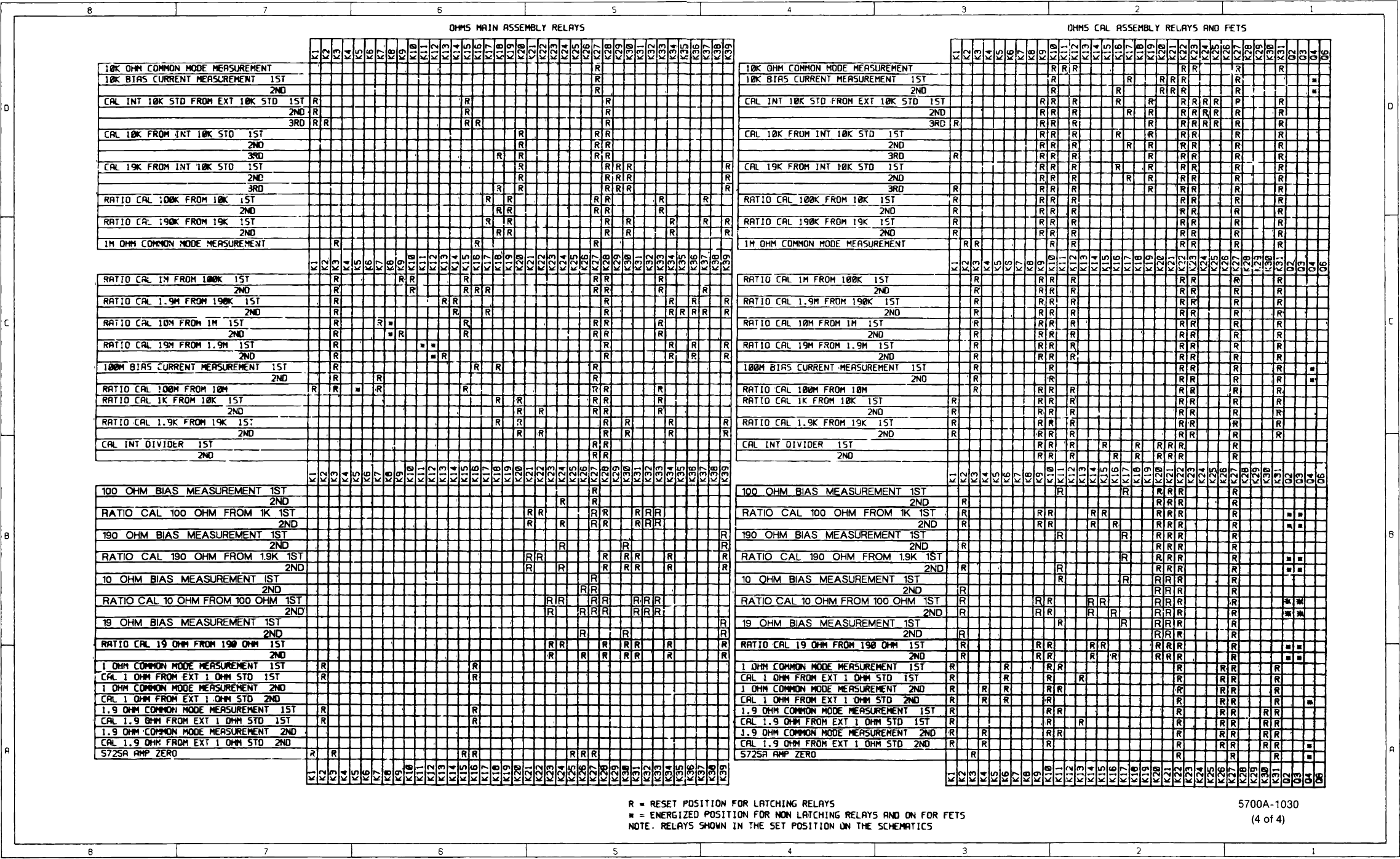
7
Schematic Diagrams
7-47
Figure 7-10. A10 Ohms Main PCA
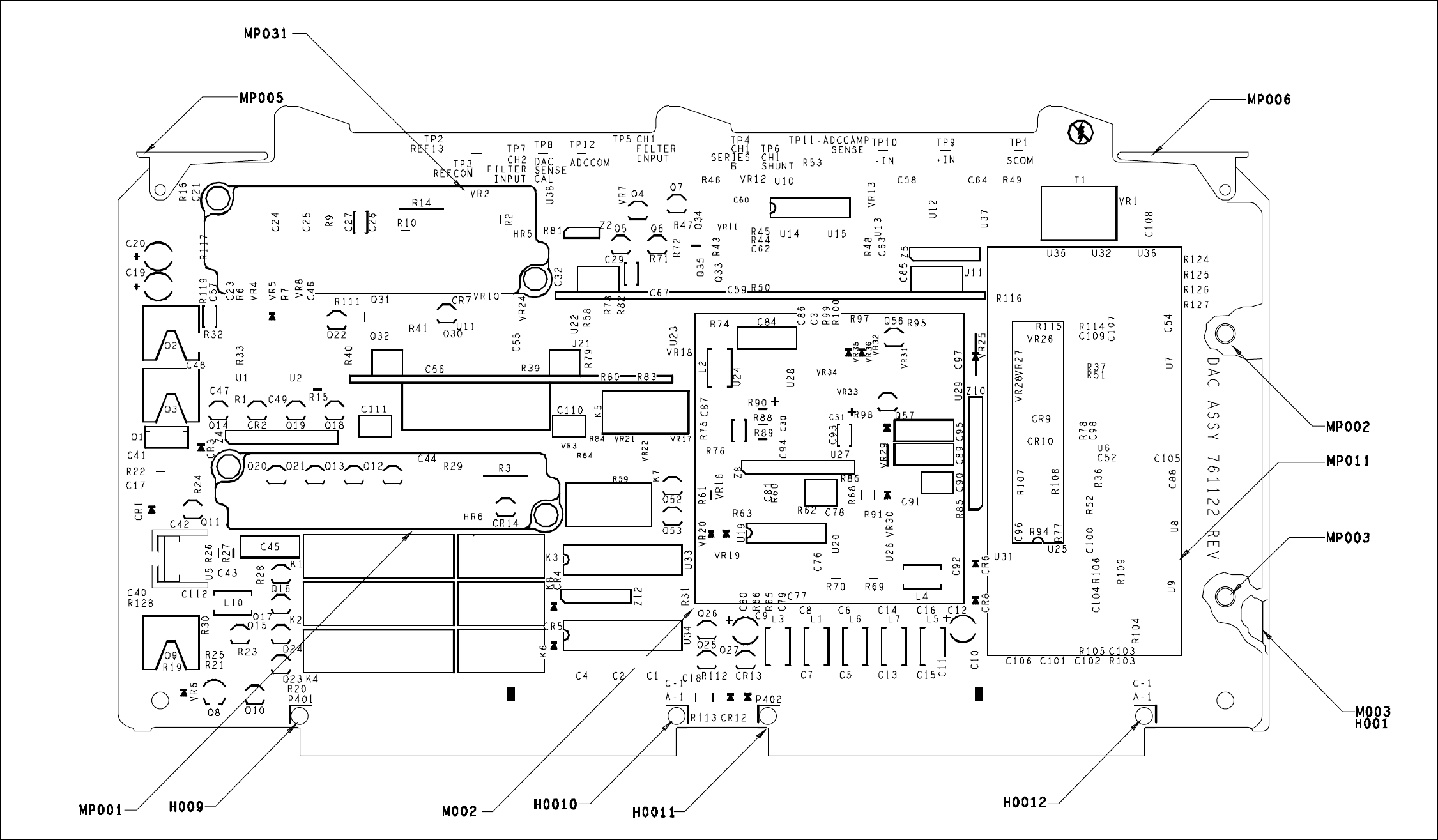
5700A/5720A Series II
Service Manual
7-48
Figure 7-11. A11 DAC PCA
5700A-7640
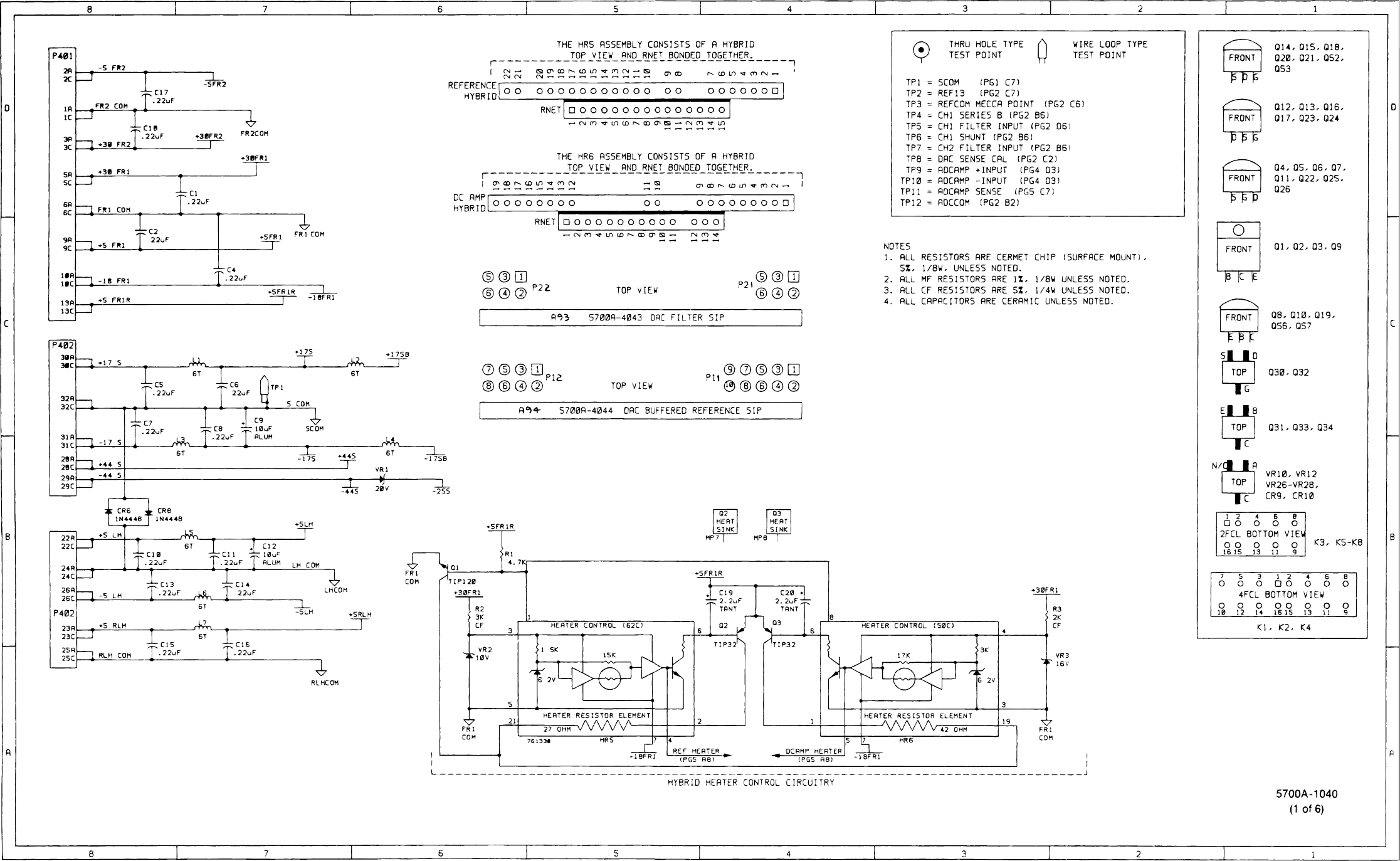
7
Schematic Diagrams
7-49
Figure 7-11. A11 DAC PCA (cont)
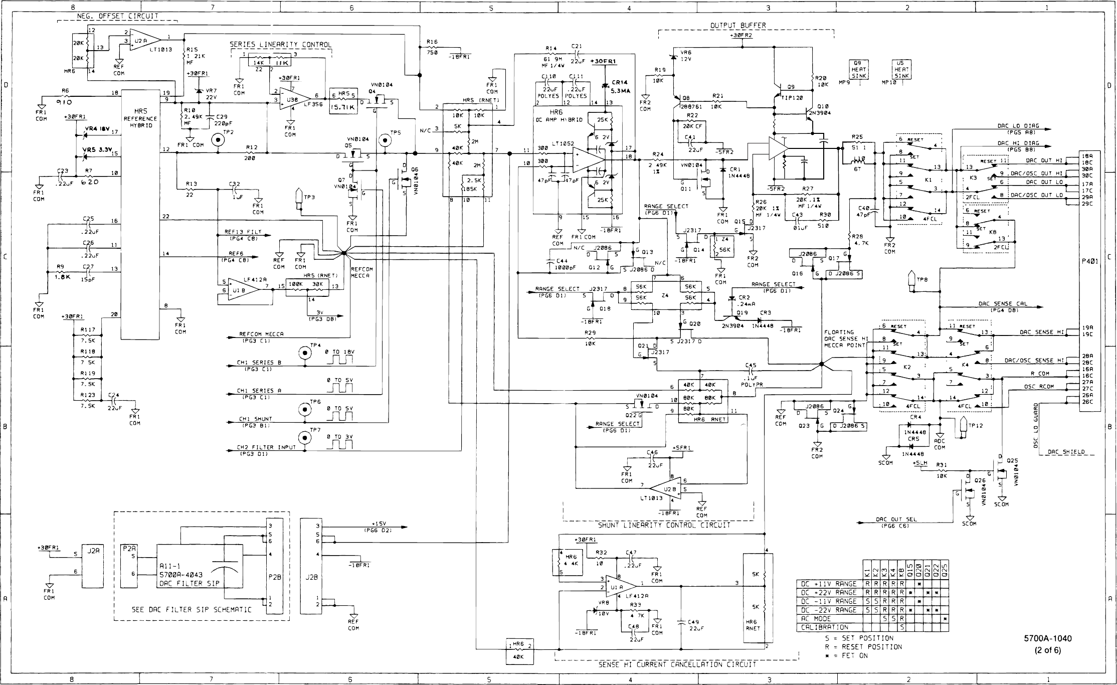
5700A/5720A Series II
Service Manual
7-50
R23
6.8
C42
22uF
1
2
3
7
6
5
4R128
200K
C112
22uF
U5
OPA527
Figure 7-11. A11 DAC PCA (cont)
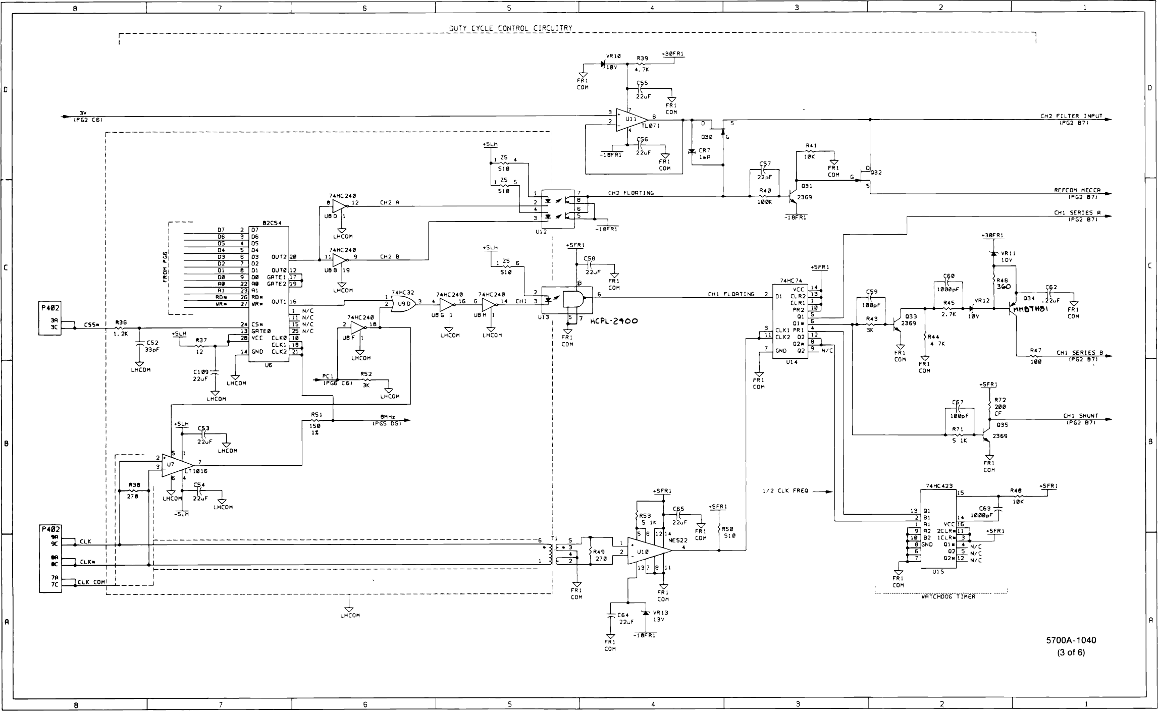
7
Schematic Diagrams
7-51
Figure 7-11. A11 DAC PCA (cont)
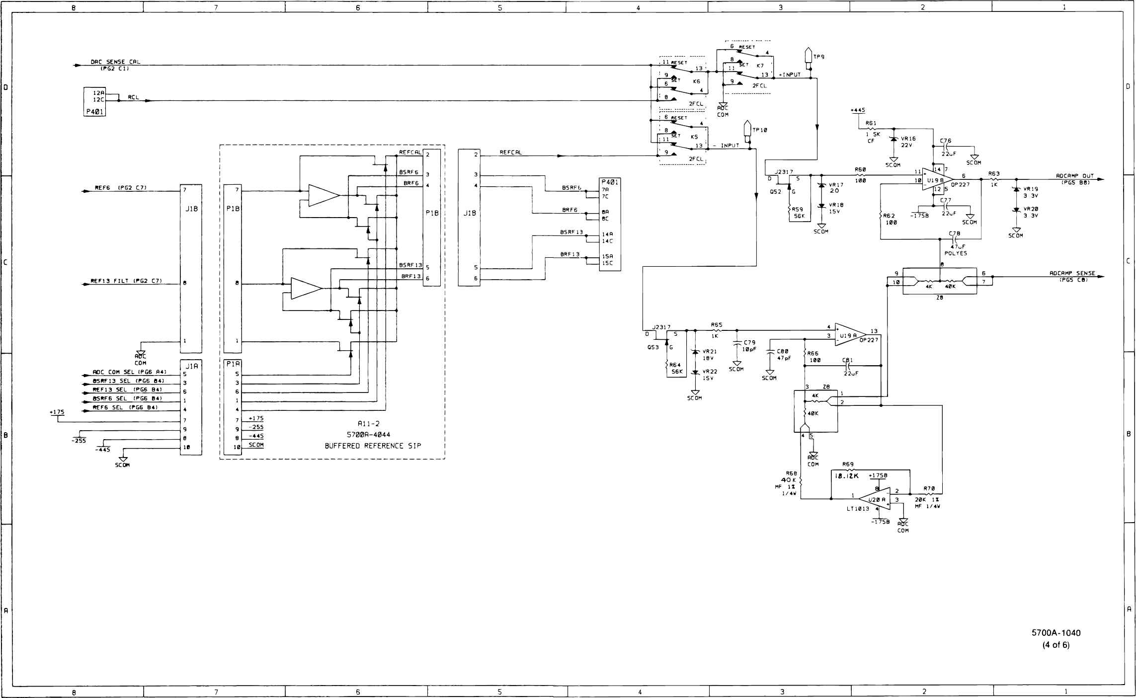
5700A/5720A Series II
Service Manual
7-52 Figure 7-11. A11 DAC PCA (cont)
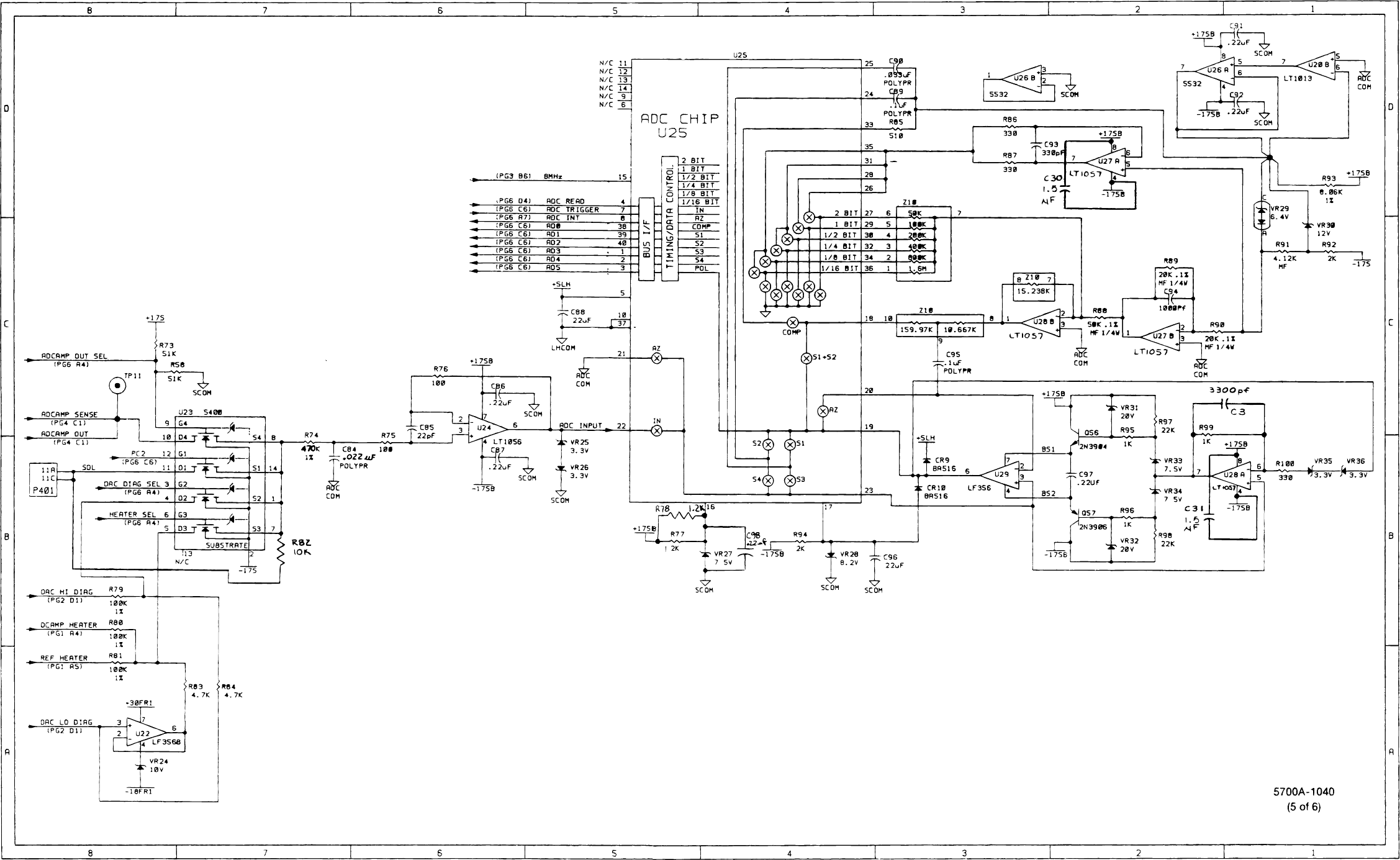
7
Schematic Diagrams
7-53
Figure 7-11. A11 DAC PCA (cont)
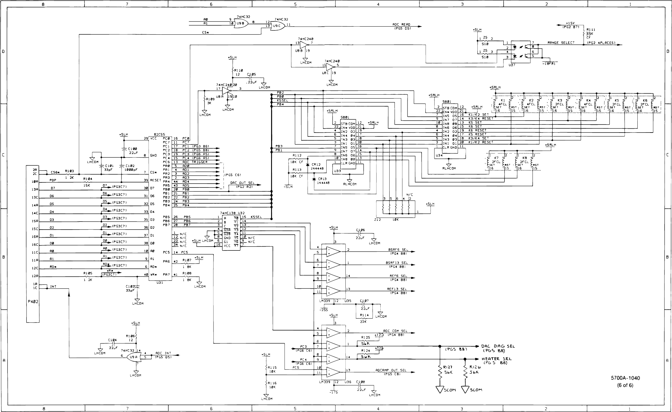
5700A/5720A Series II
Service Manual
7-54
Figure 7-11. A11 DAC PCA (cont)
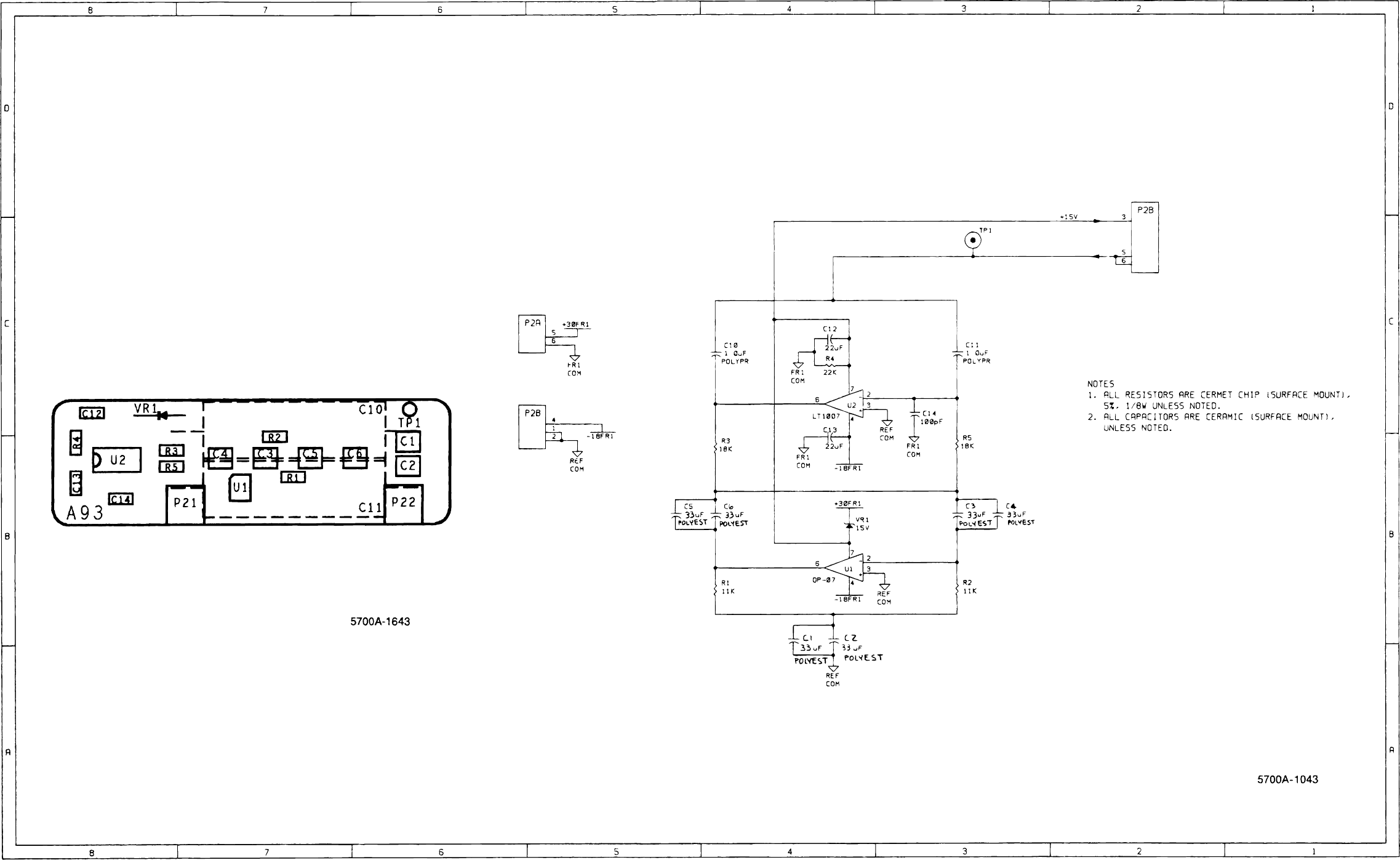
7
Schematic Diagrams
7-55
Figure 7-12. A11A1 DAC Filter SIP PCA
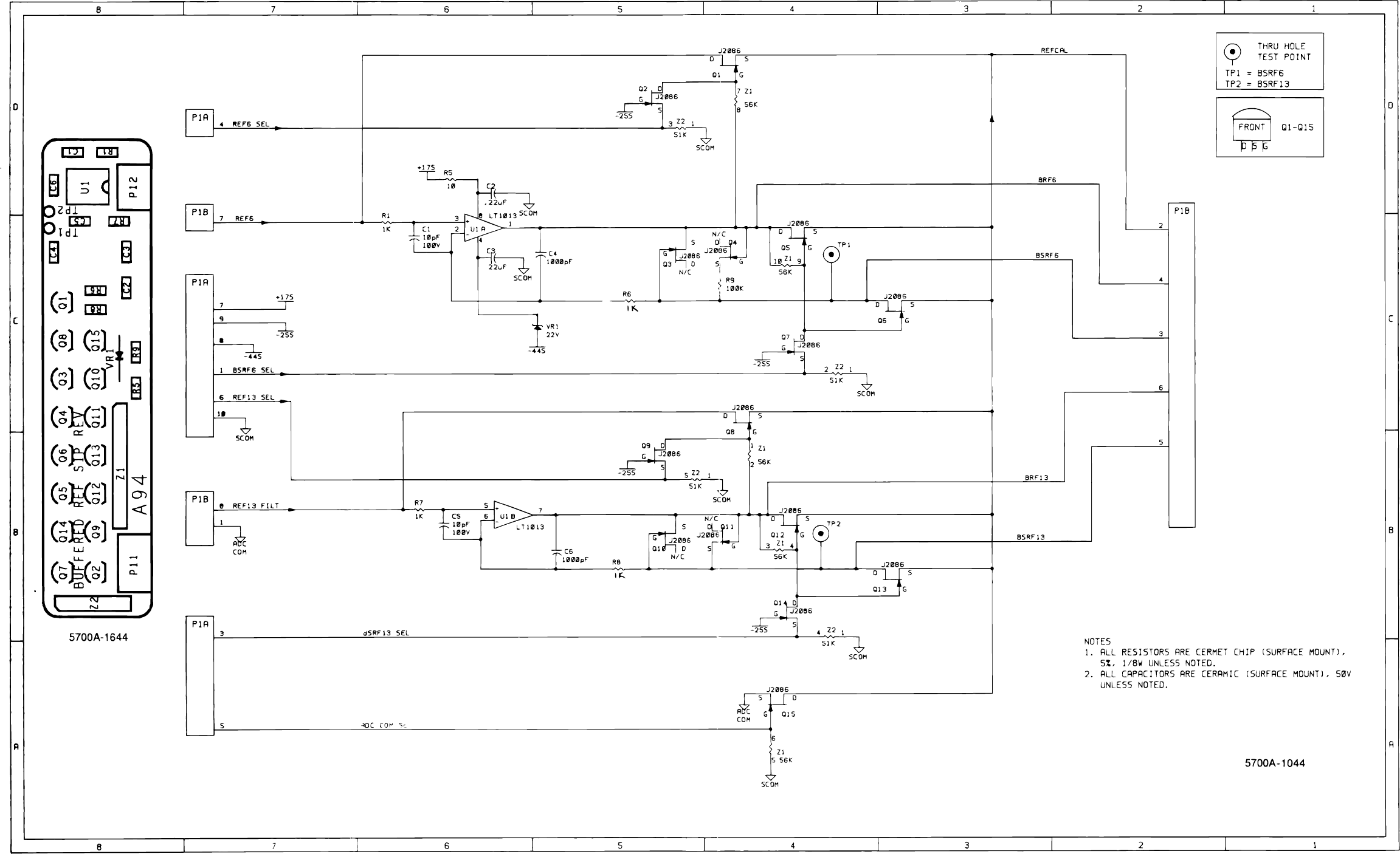
5700A/5720A Series II
Service Manual
7-56 Figure 7-13. A1142 DAC Buffered Reference SIP PCA
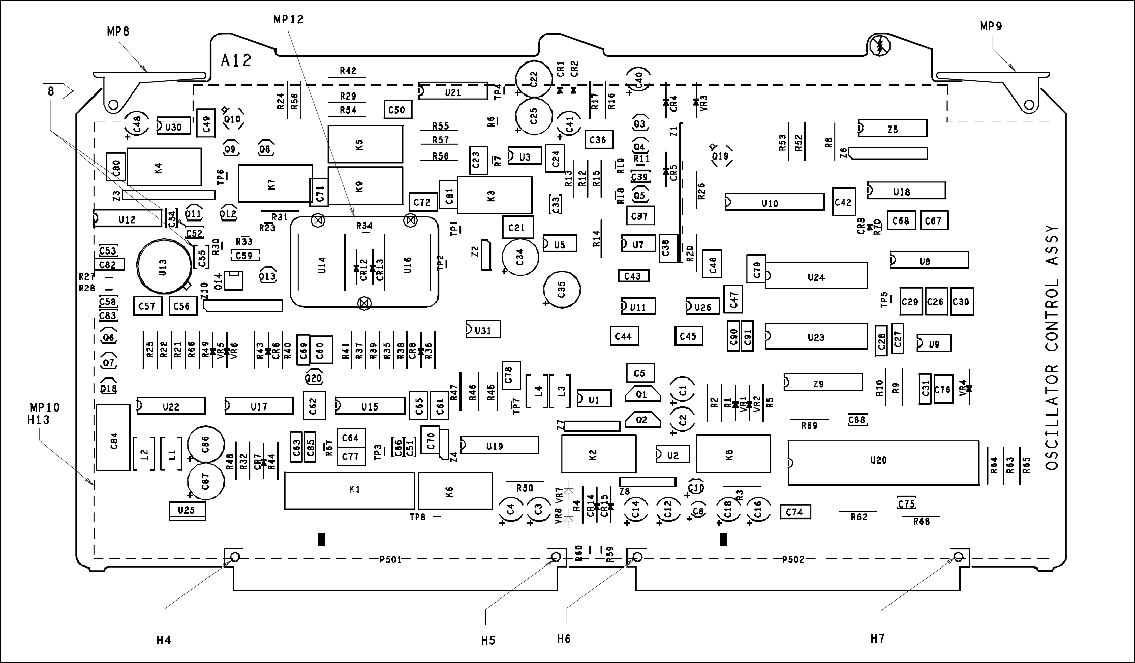
7
Schematic Diagrams
7-57
5700A-7650
Figure 7-14. A12 Oscillator Control PCA (cont)
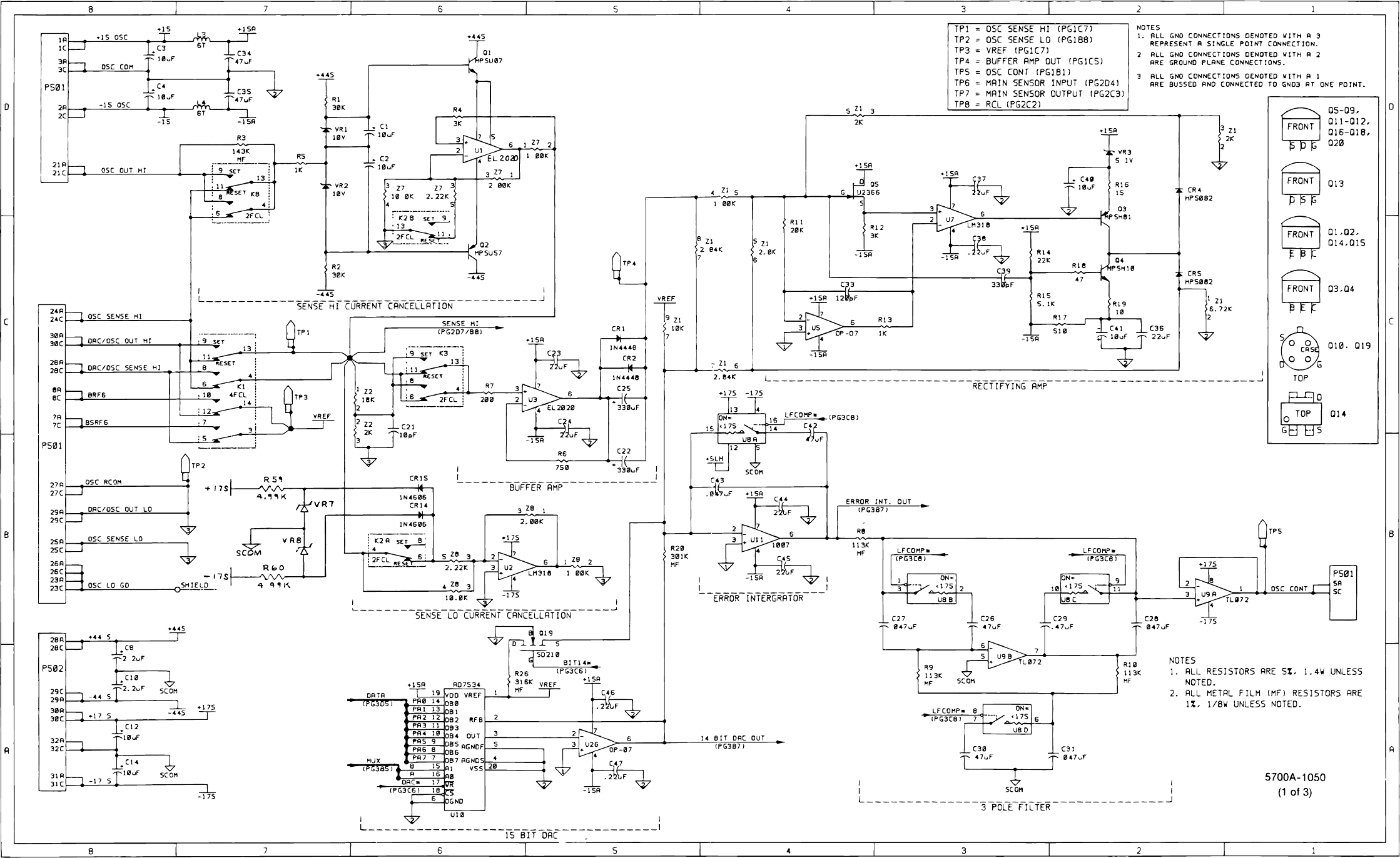
5700A/5720A Series II
Service Manual
7-58
DG211
DG211
DG211
DG211
DG211
3. ALL GND CONNECTIONS DENOTED WITH
A 1 ARE BUSSED AND CONNECTED TO GND3
AT ONE POINT.
4. C5 AND C55 ARE NOT INSTALLED.
Figure 7-14. A12 Oscillator Control PCA (cont)
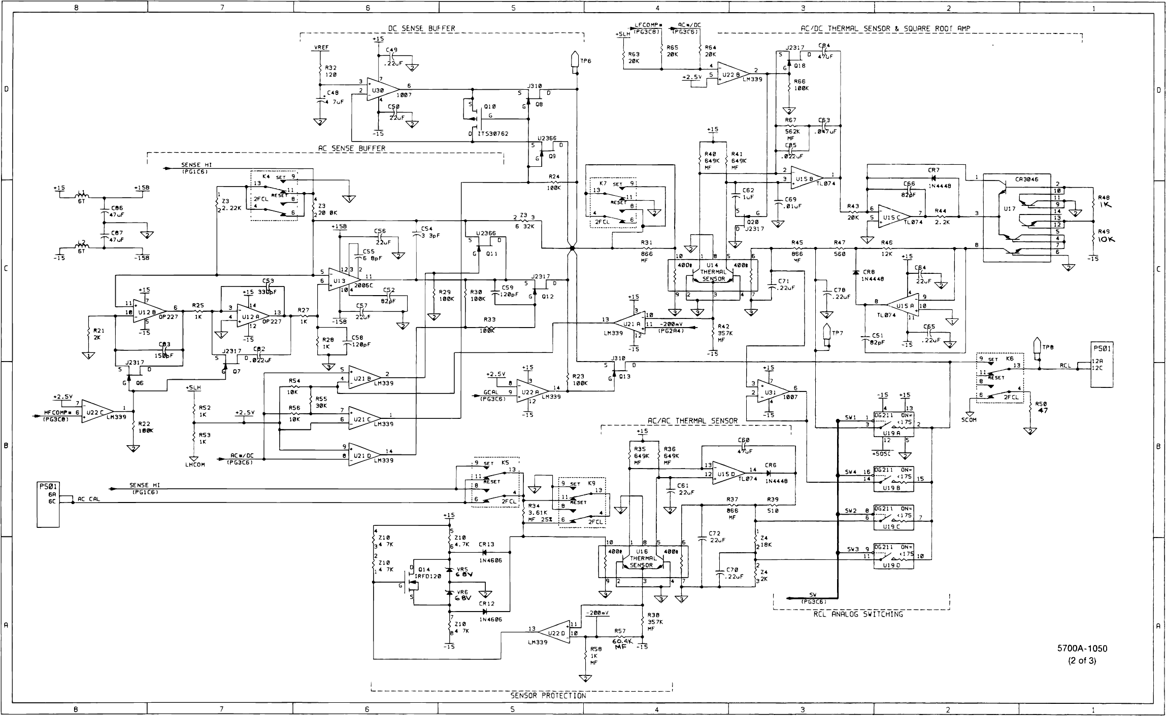
7
Schematic Diagrams
7-59
Figure 7-14. A12 Oscillator Control PCA (cont)
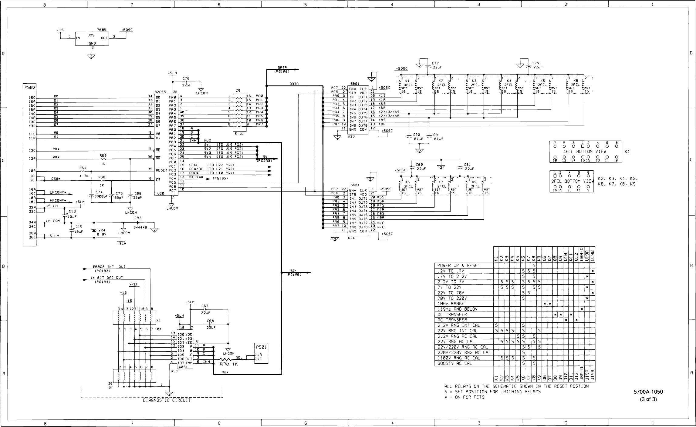
5700A/5720A Series II
Service Manual
7-60 Figure 7-14. A12 Oscillator Control PCA (cont)
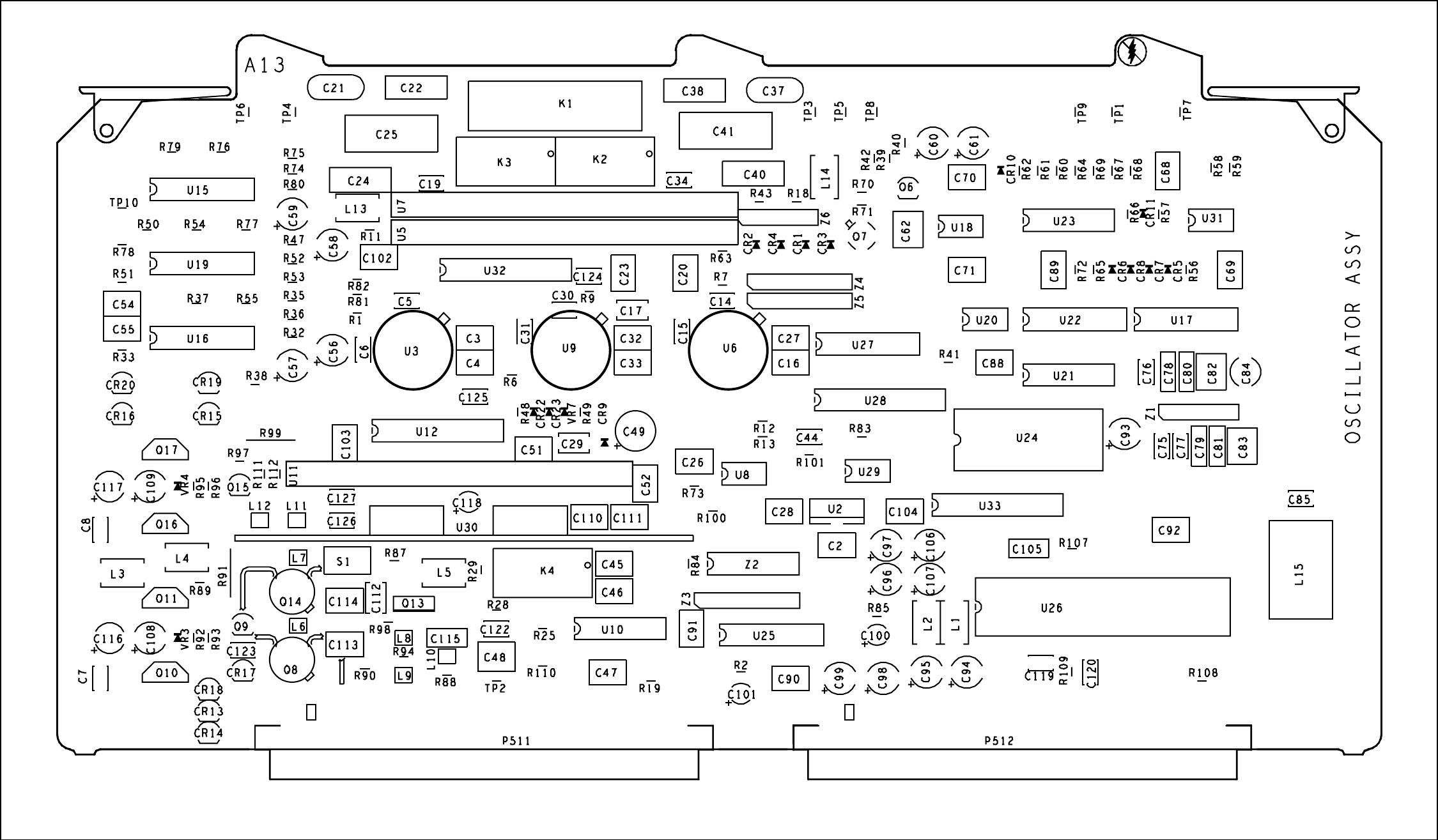
7
Schematic Diagrams
7-61
5700A-1651
Figure 7-15. A13 Oscillator Output PCA
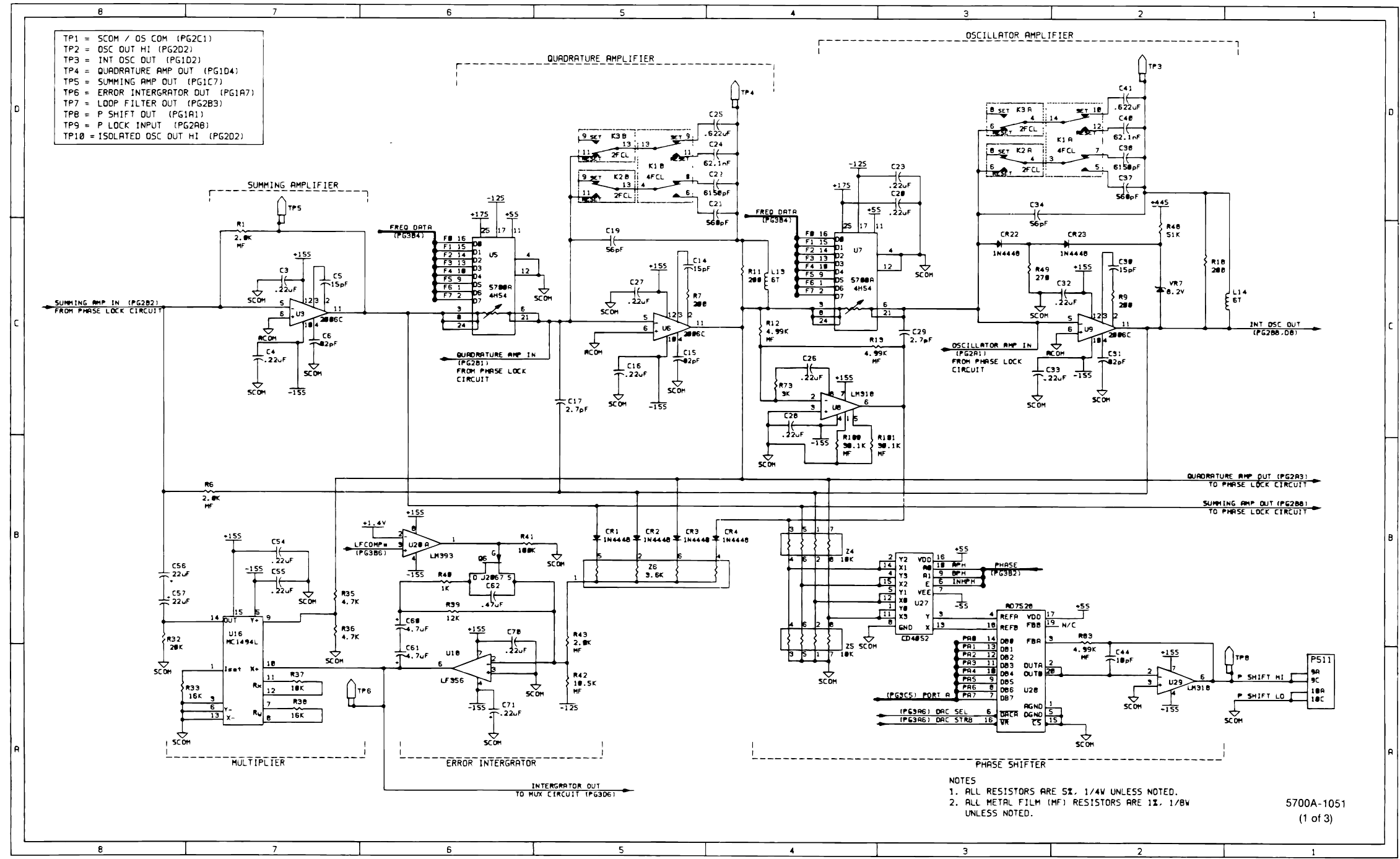
5700A/5720A Series II
Service Manual
7-62
Figure 7-15. A13 Oscillator Output PCA (cont)
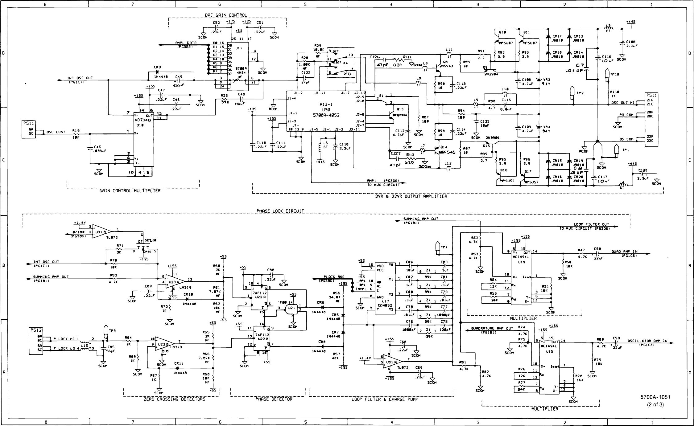
7
Schematic Diagrams
7-63
Figure 7-15. A13 Oscillator Output PCA (cont)
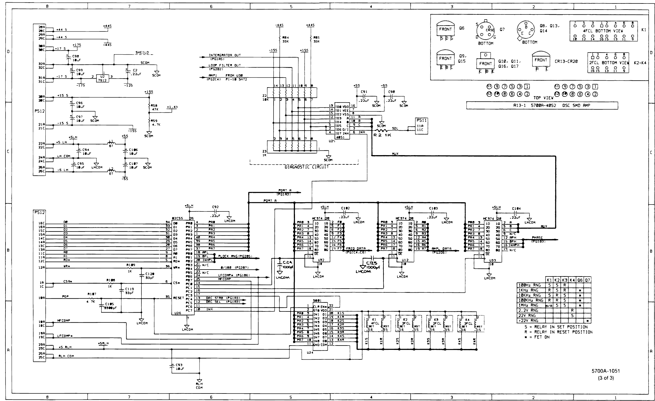
5700A/5720A Series II
Service Manual
7-64
Figure 7-15. A13 Oscillator Output PCA (cont)
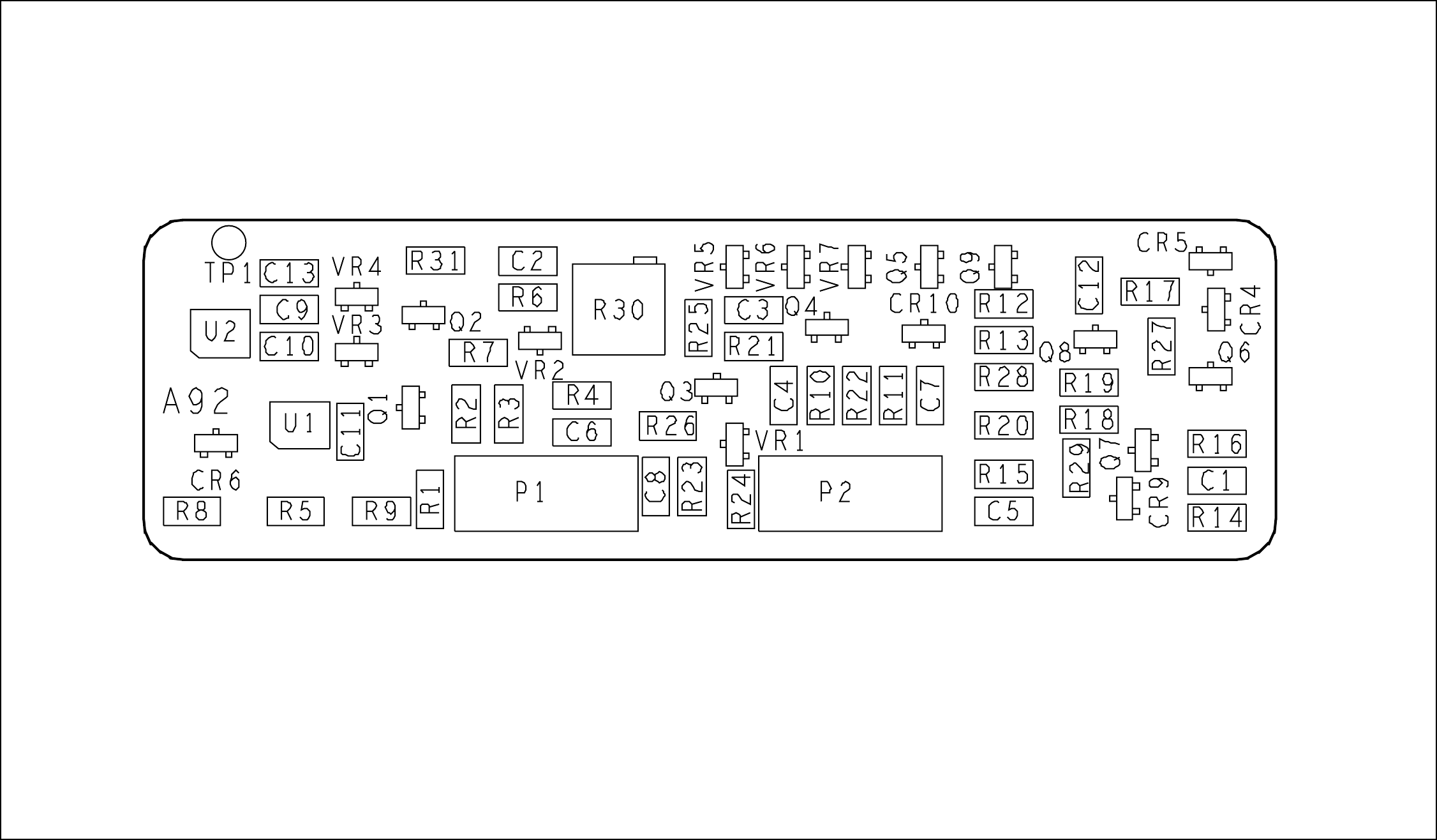
7
Schematic Diagrams
7-65
5700A-1652
Figure 7-16. A13A1 Oscillator Wideband SMD PCA
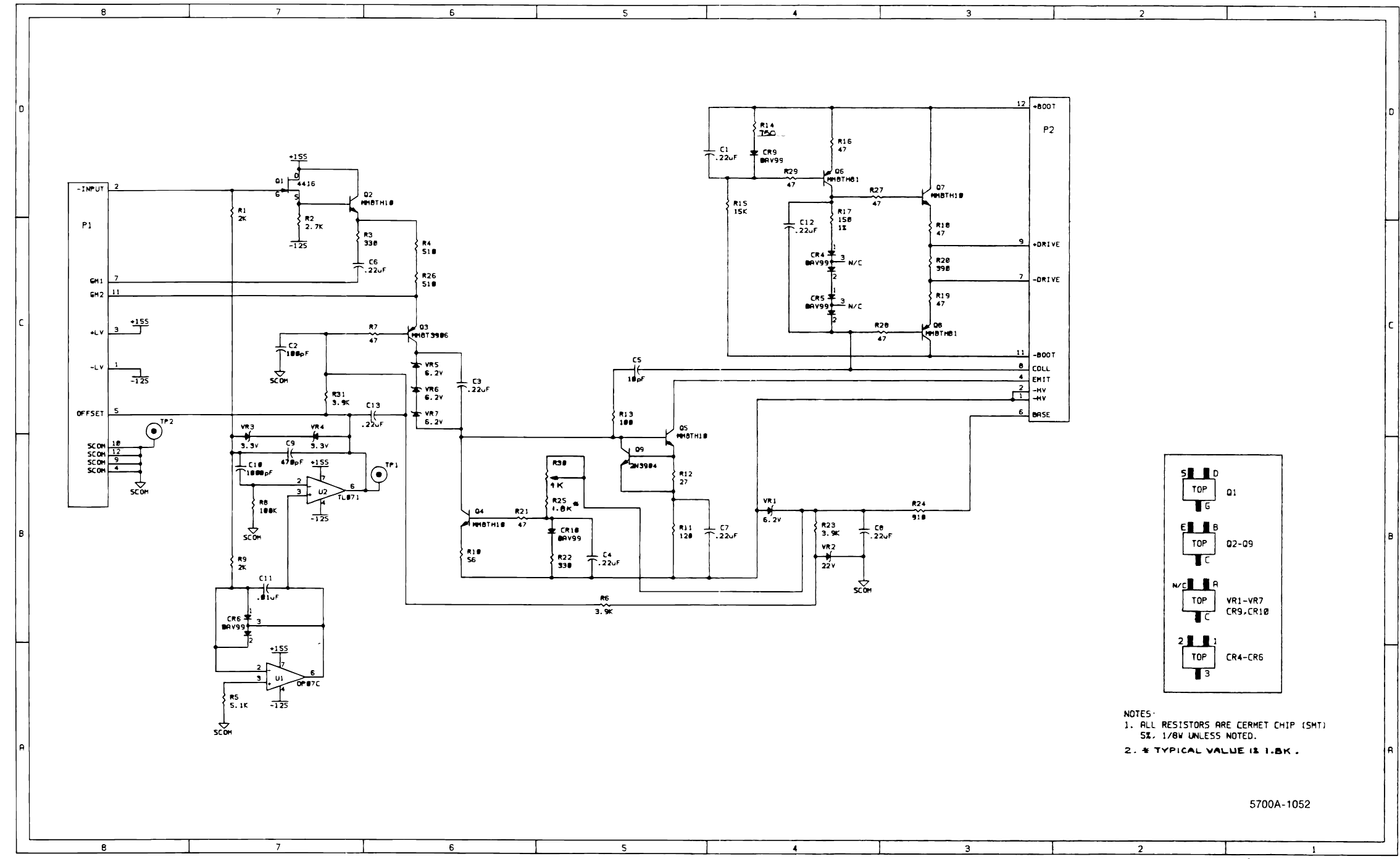
5700A/5720A Series II
Service Manual
7-66
Figure 7-16. A13A1 Oscillator Wideband SMD PCA (cont)
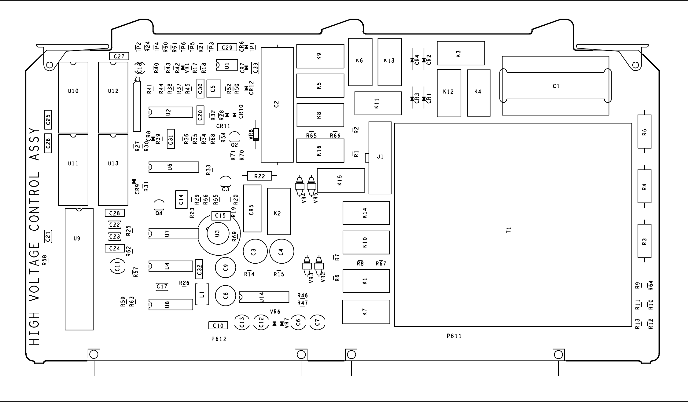
7
Schematic Diagrams
7-67
5700A-1661
Figure 7-17. A14 High Voltage Control PCA
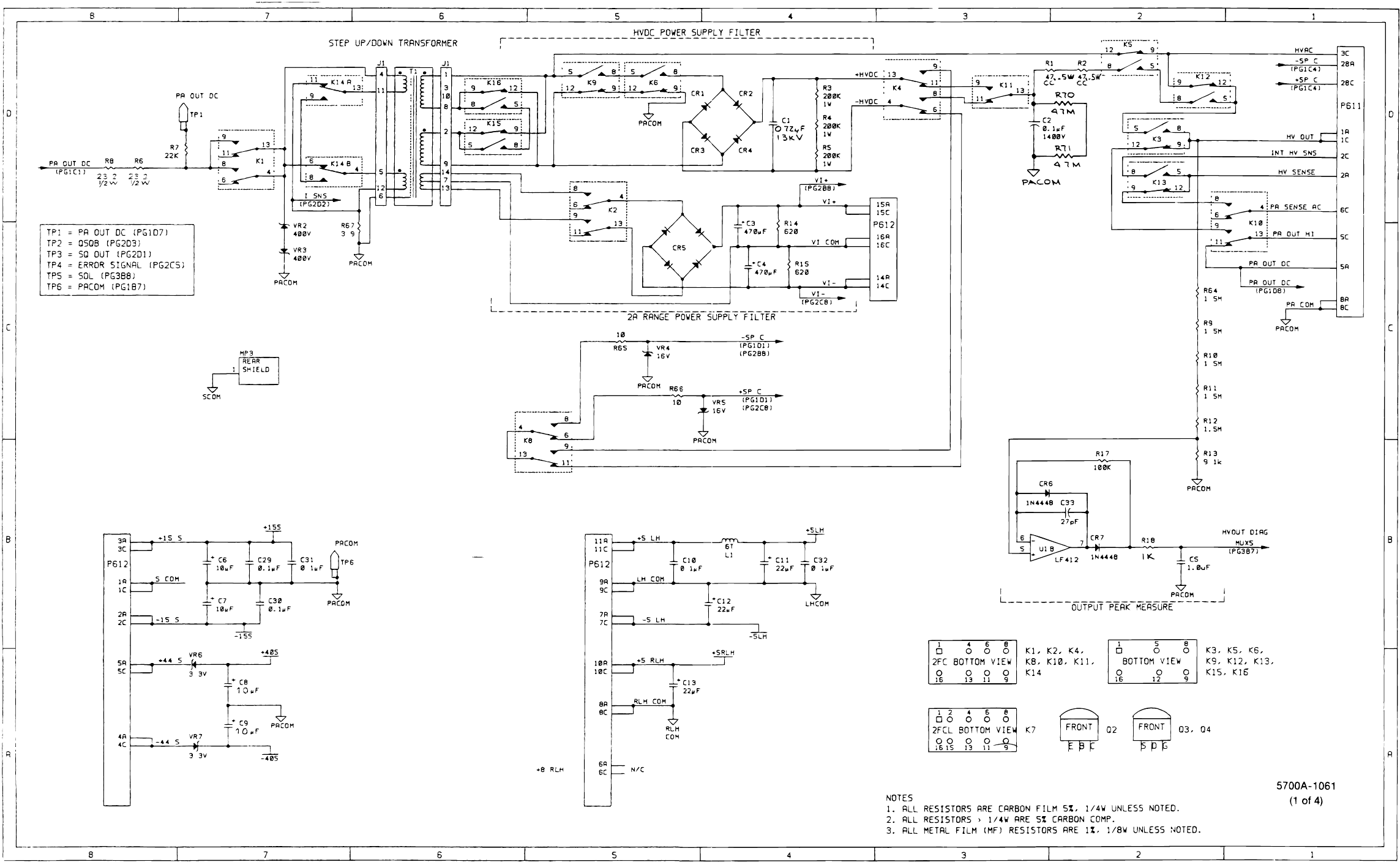
5700A/5720A Series II
Service Manual
7-68 Figure 7-17. A14 High Voltage Control PCA (cont)
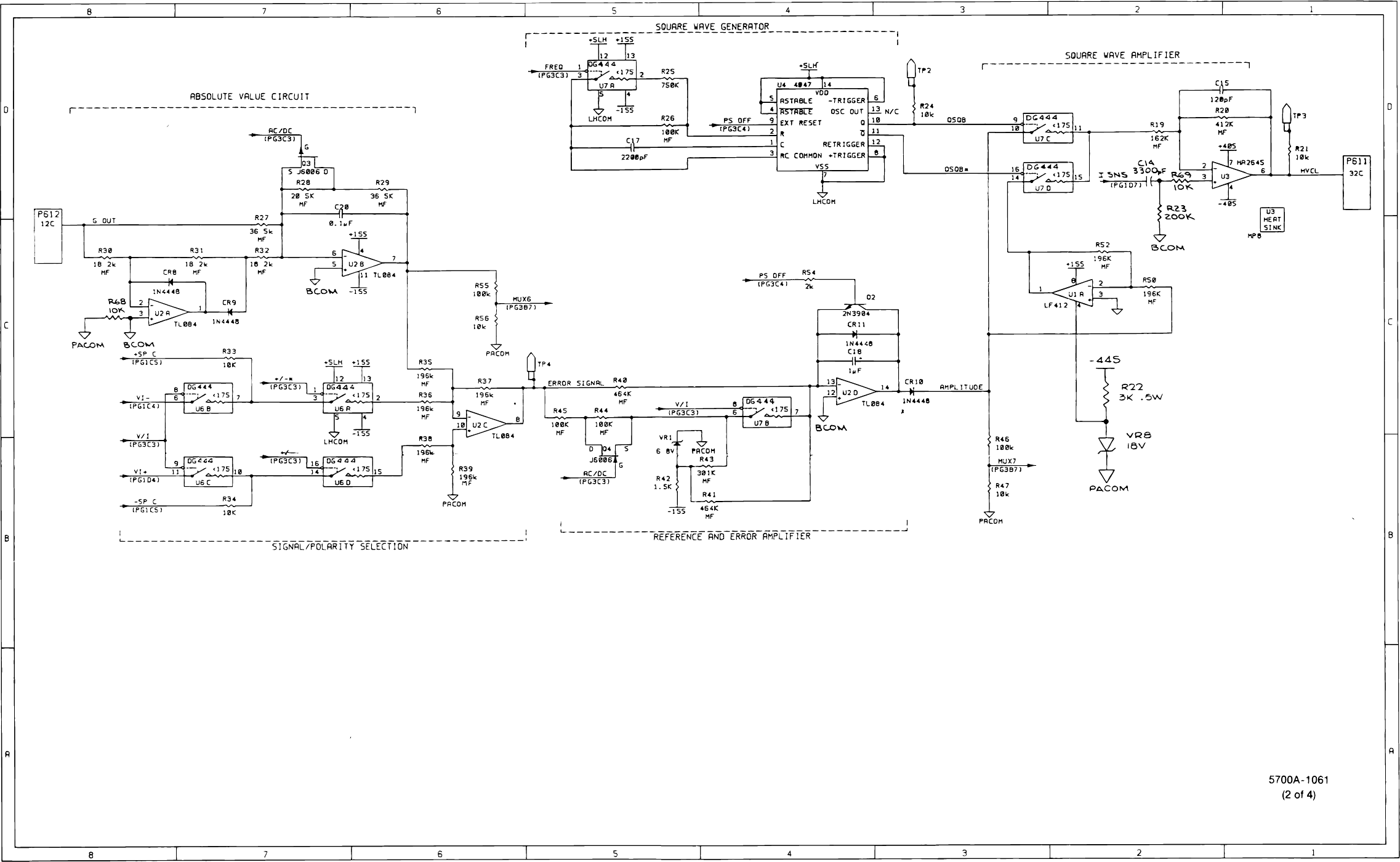
7
Schematic Diagrams
7-69
Figure 7-17. A14 High Voltage Control PCA (cont)
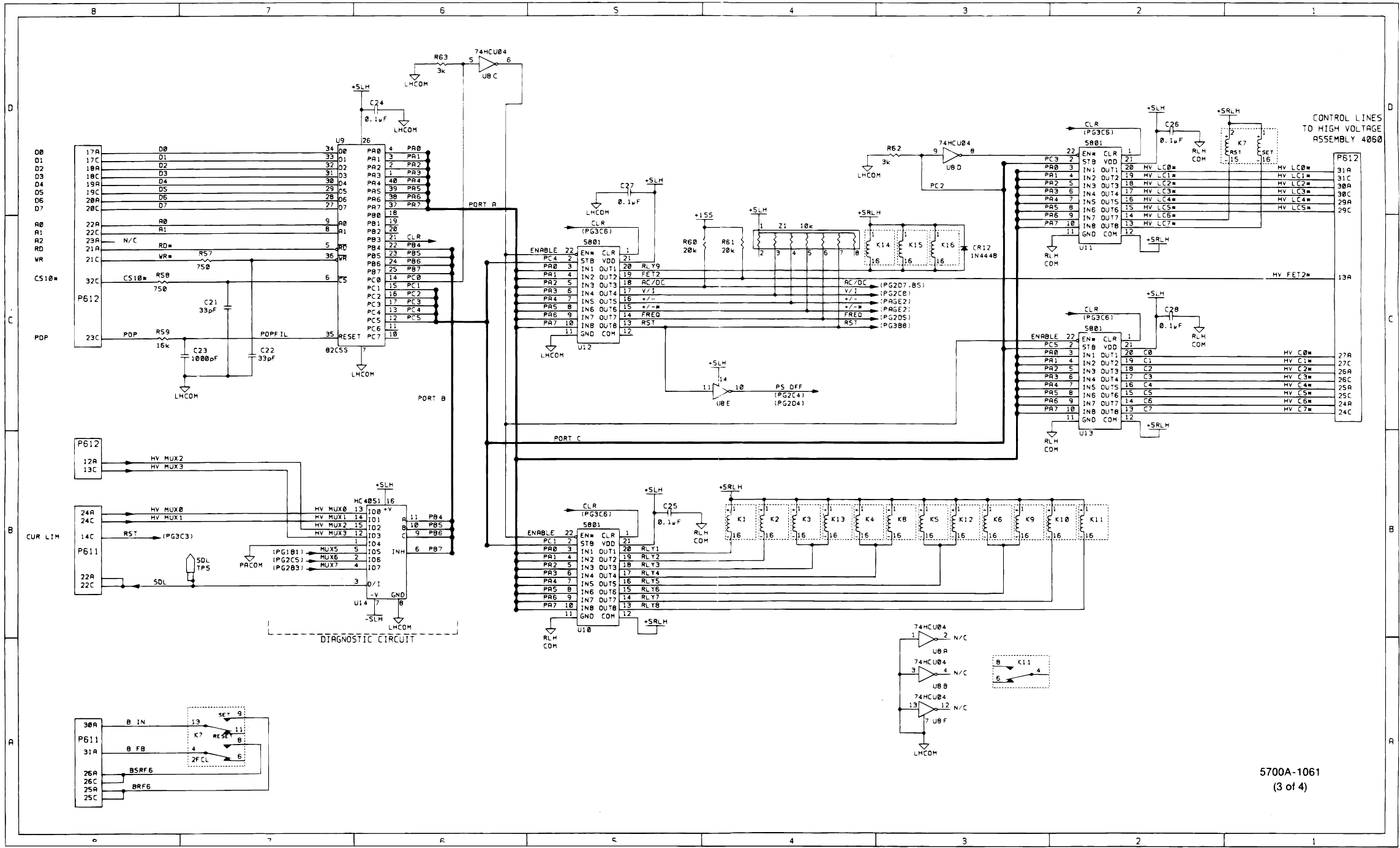
5700A/5720A Series II
Service Manual
7-70
Figure 7-17. A14 High Voltage Control PCA (cont)
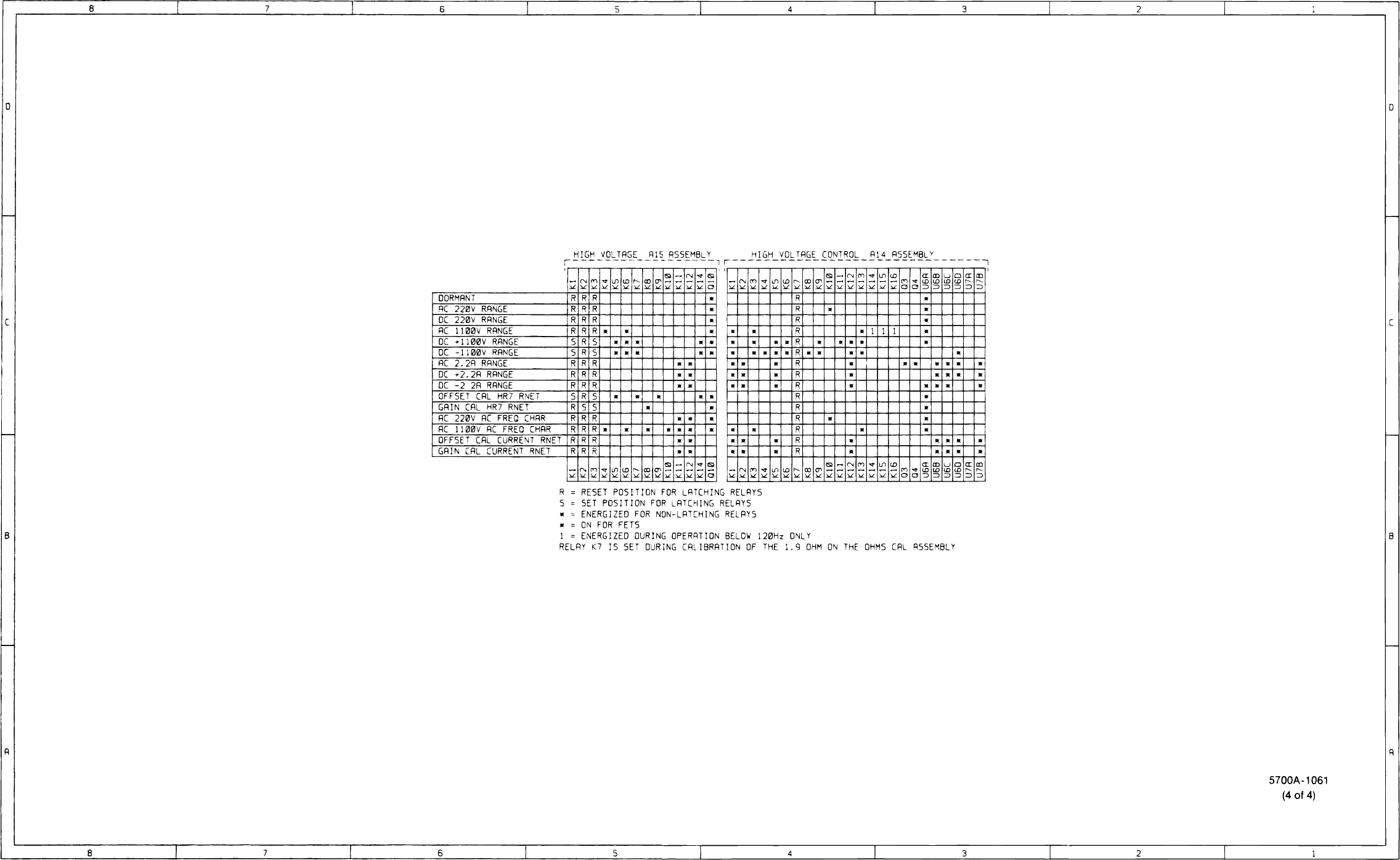
7
Schematic Diagrams
7-71
Figure 7-17. A14 High Voltage Control PCA (cont)
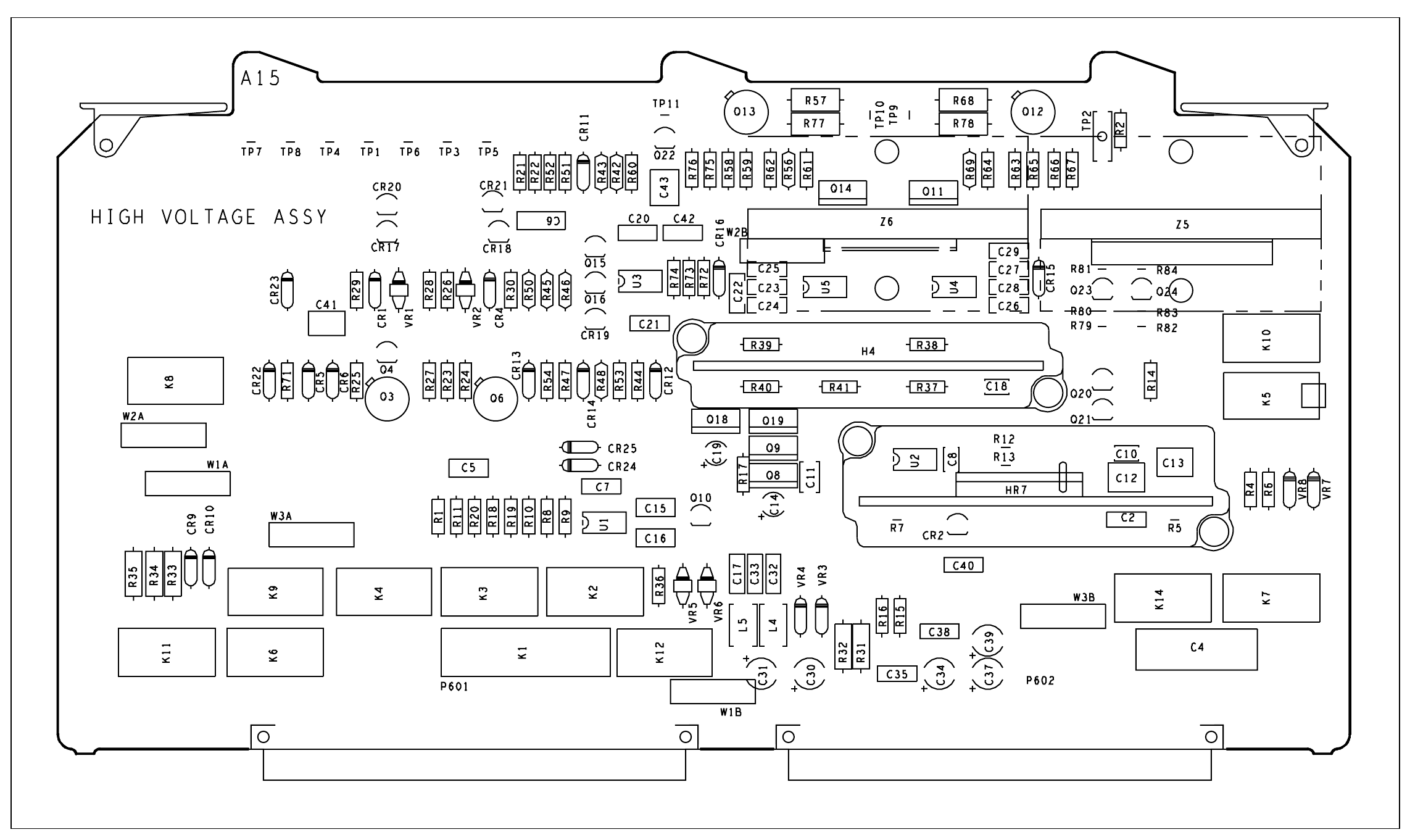
5700A/5720A Series II
Service Manual
7-72
5700A-1660
Figure 7-18. A15 High Voltage/ High Current PCA

7
Schematic Diagrams
7-73
Figure 7-18. A15 High Voltage/High Current PCA (cont)
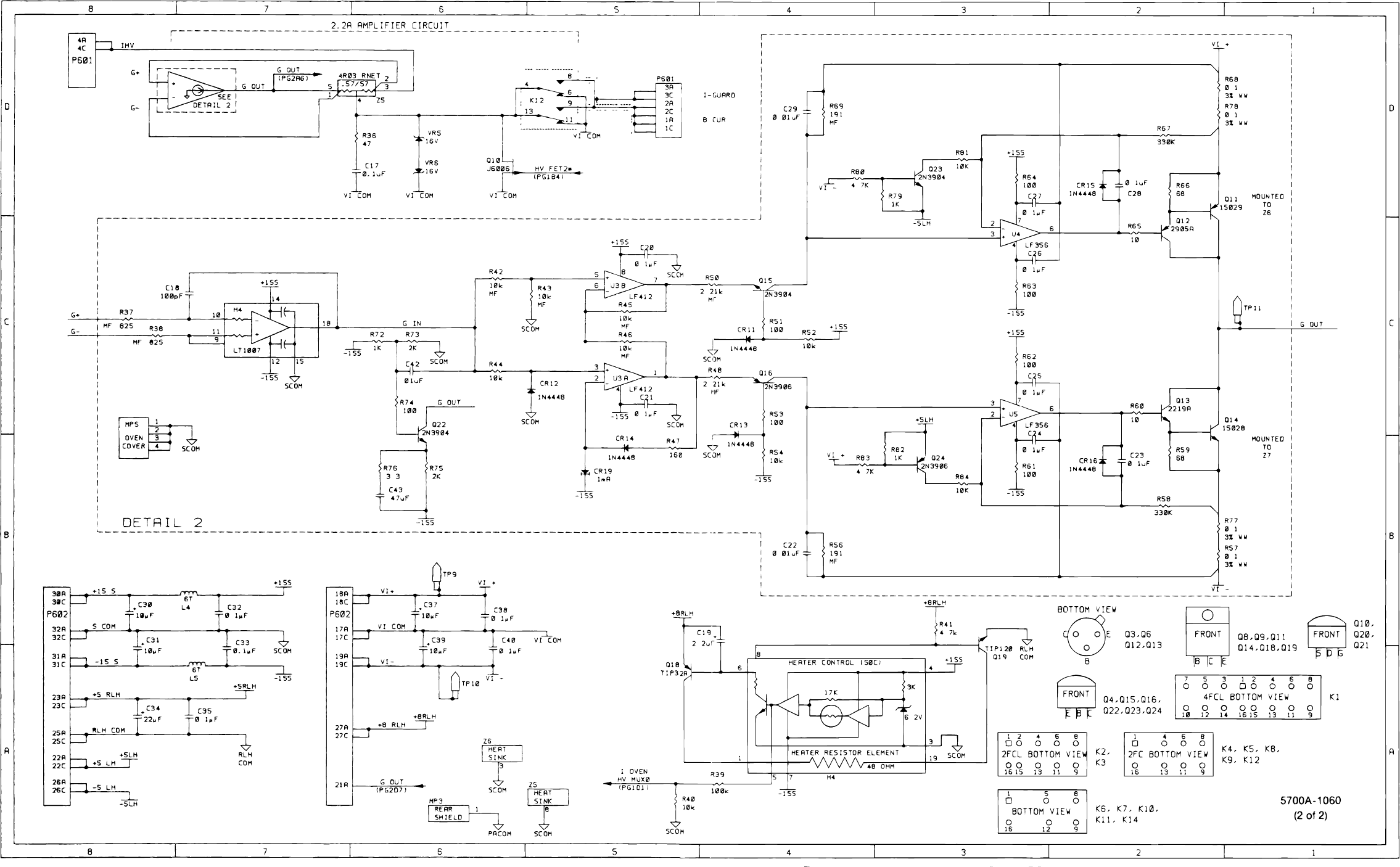
5700A/5720A Series II
Service Manual
7-74 Figure 7-18. A15 High Voltage/High Current PCA (cont)
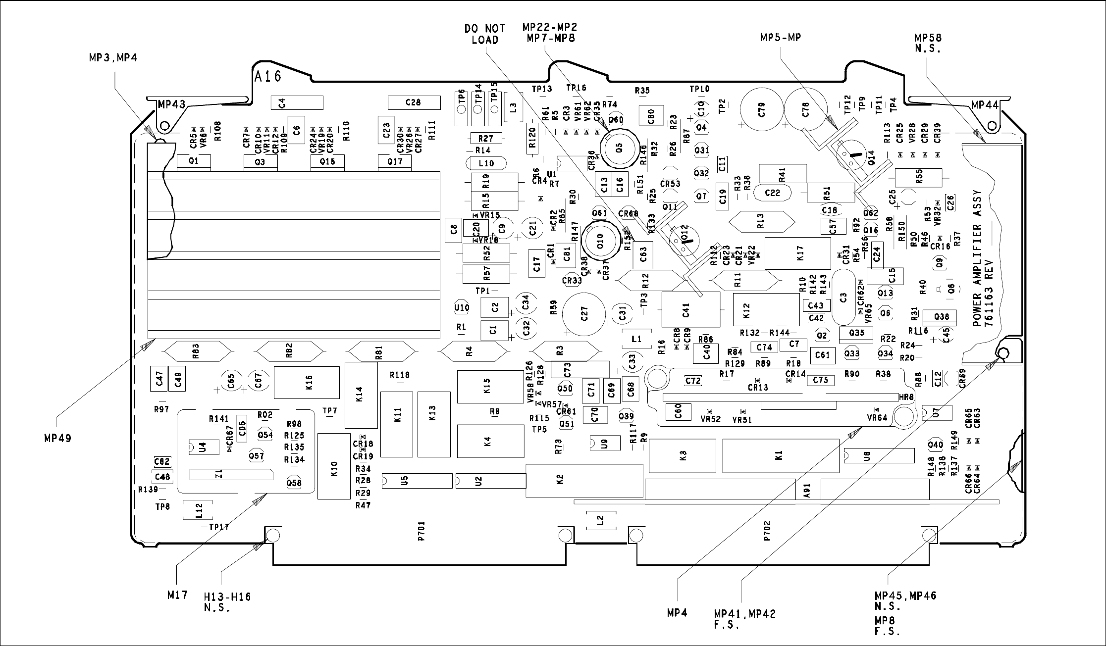
7
Schematic Diagrams
7-75
5700A-7670
Figure 7-19. A16 Power Amplifier PCA
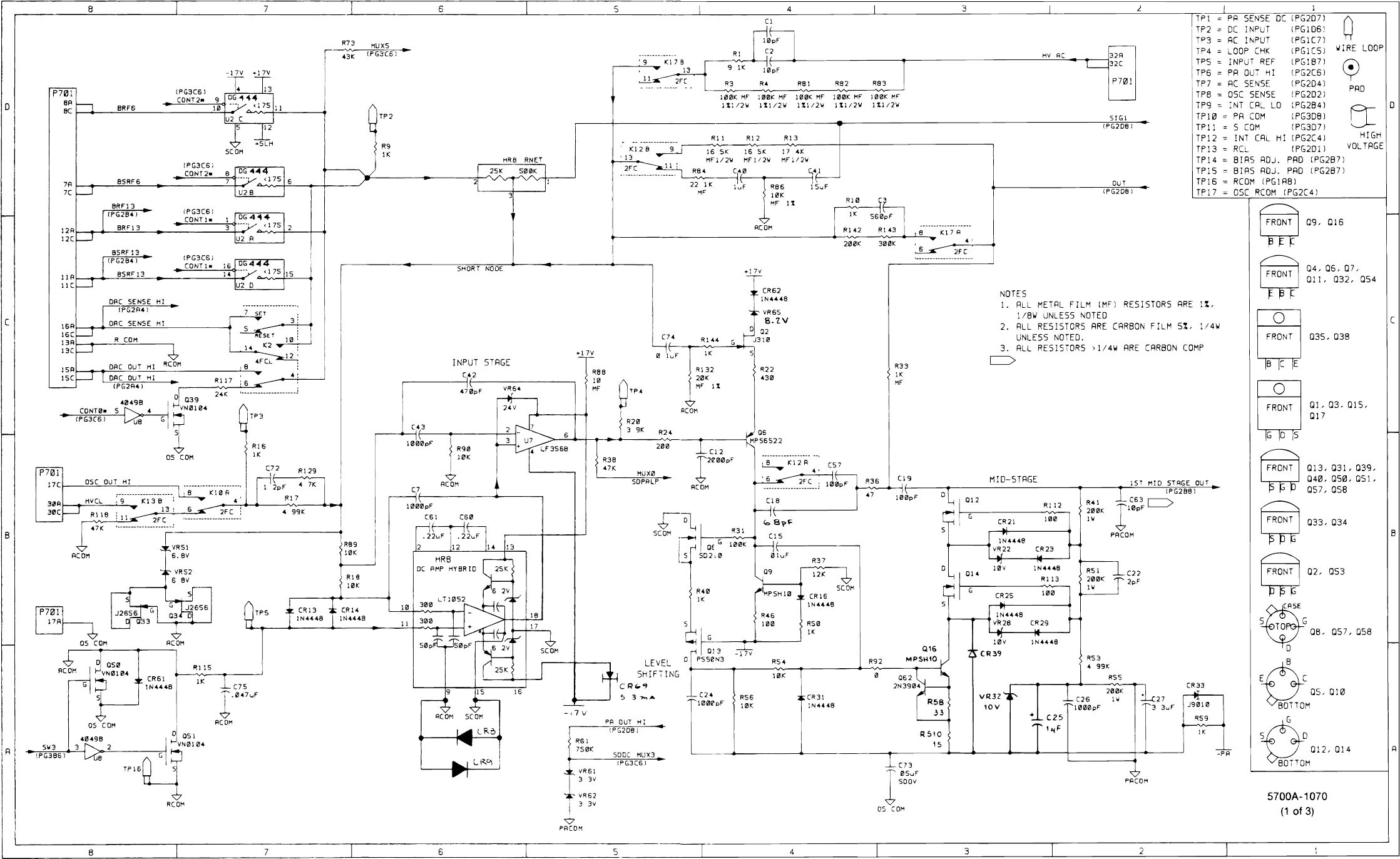
5700A/5720A Series II
Service Manual
7-76
4. NOT INSTALLED
STD1N890
STD1N890
4.
Figure 7-19. A16 Power Amplifier PCA (cont)
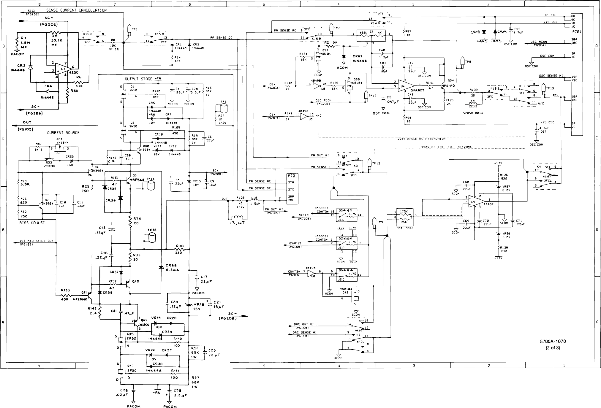
7
Schematic Diagrams
7-77
Figure 7-19. A16 Power Amplifier PCA (cont)
10 M
2N4044
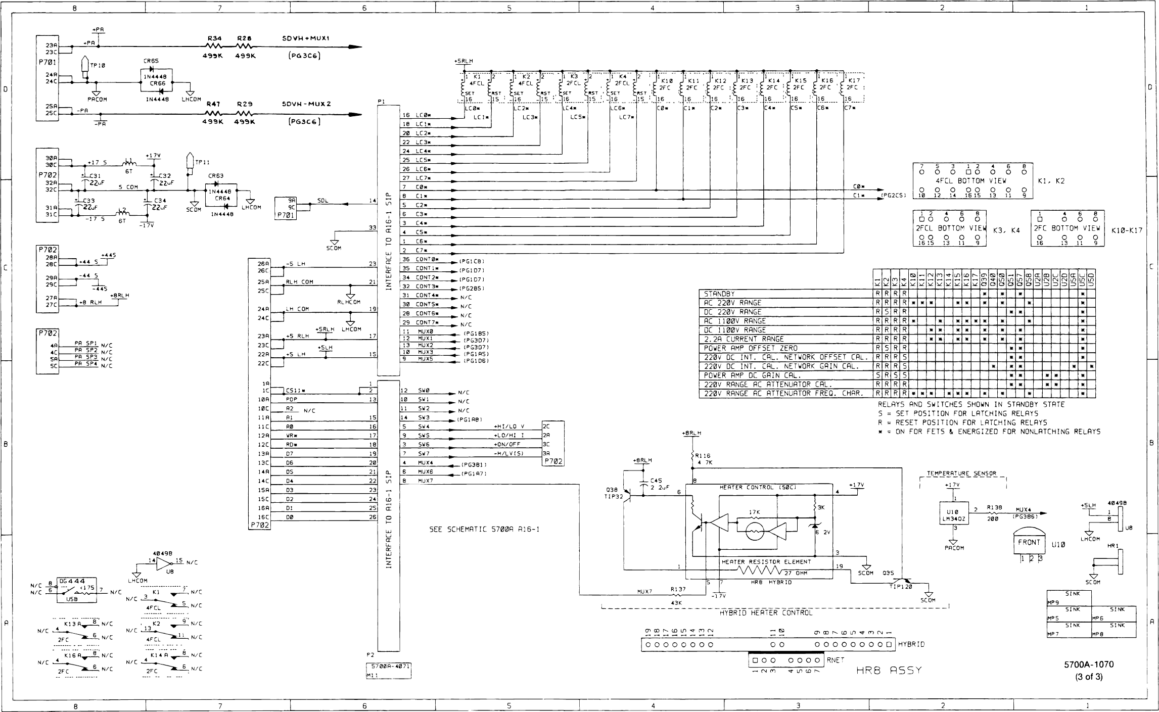
5700A/5720A Series II
Service Manual
7-78 Figure 7-19. A16 Power Amplifier PCA (cont)
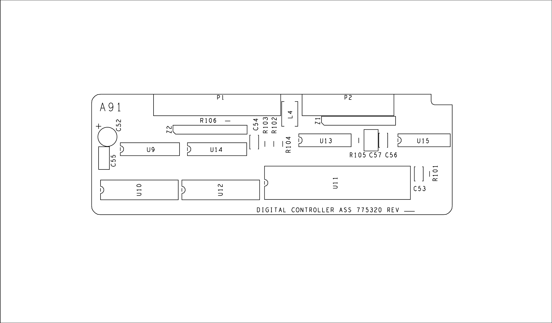
7
Schematic Diagrams
7-79
5700A-1671
Figure 7-20. A16A1 Power Amplifier Digitial
Control SIP PCA
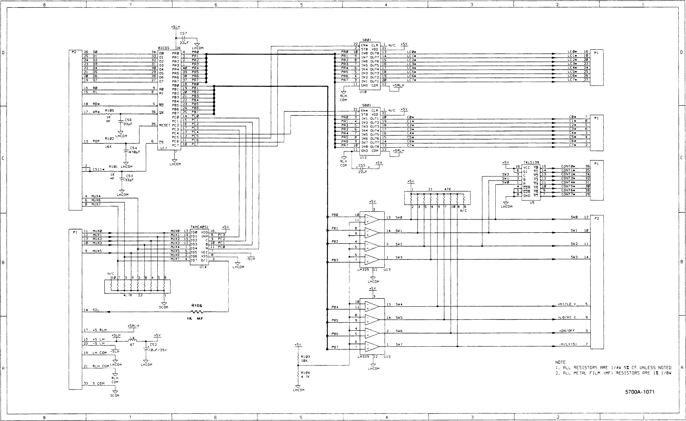
5700A/5720A Series II
Service Manual
7-80 Figure 7-20. A161A1 Power Amplifier Digital
Control SIP PCA (cont)
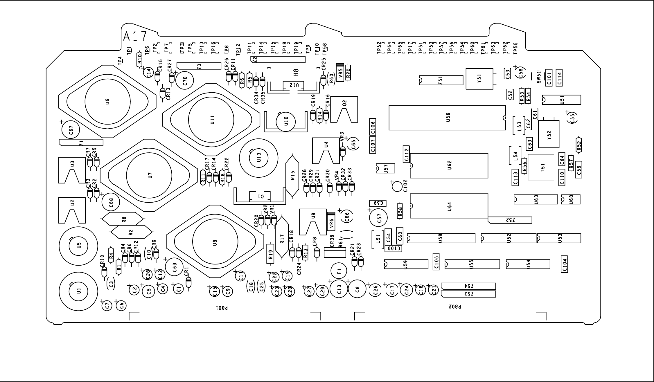
7
Schematic Diagrams
7-81
Figure 7-21. A17 Regulator/Guard Crossing PCA
5700A-1680
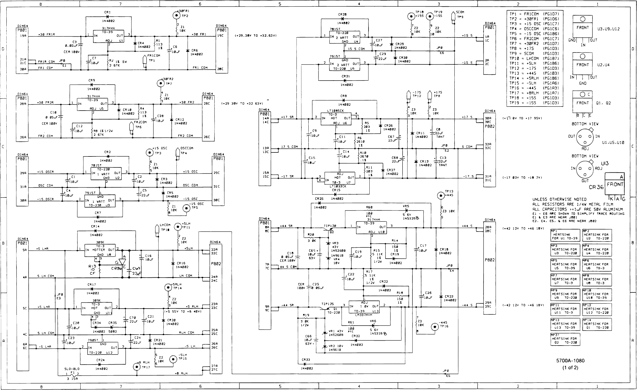
5700A/5720A Series II
Service Manual
7-82
Figure 7-21. A17 Regulator/Guard Crossing PCA (cont)
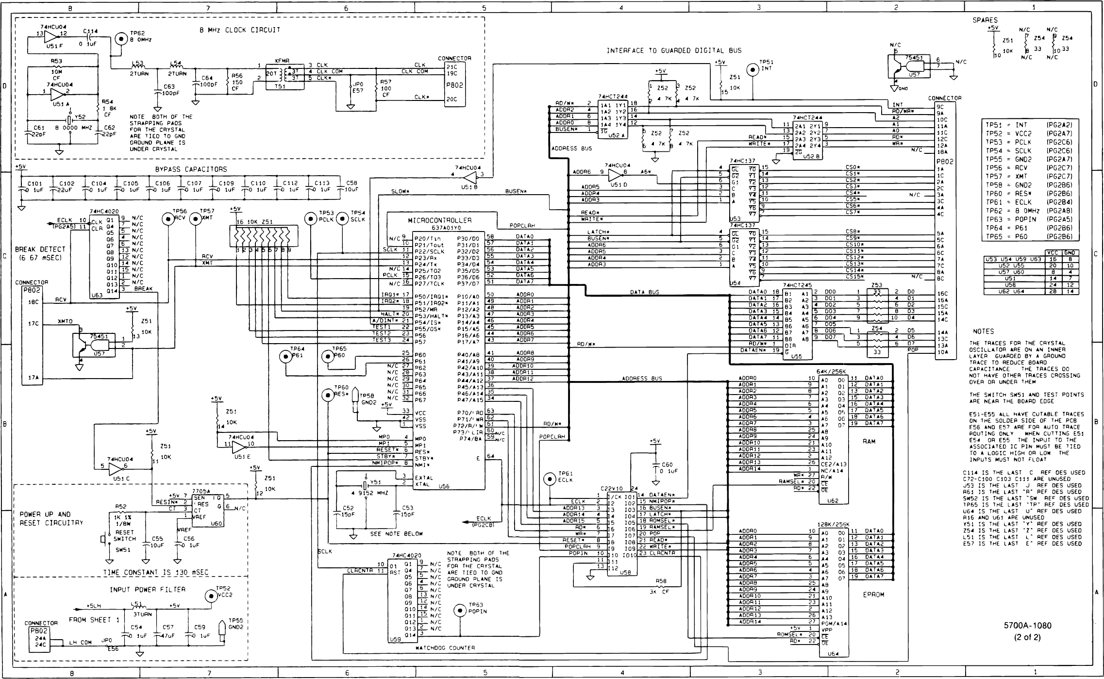
7
Schematic Diagrams
7-83
Figure 7-21. A17 Regulator/Guard Crossing PCA (cont)
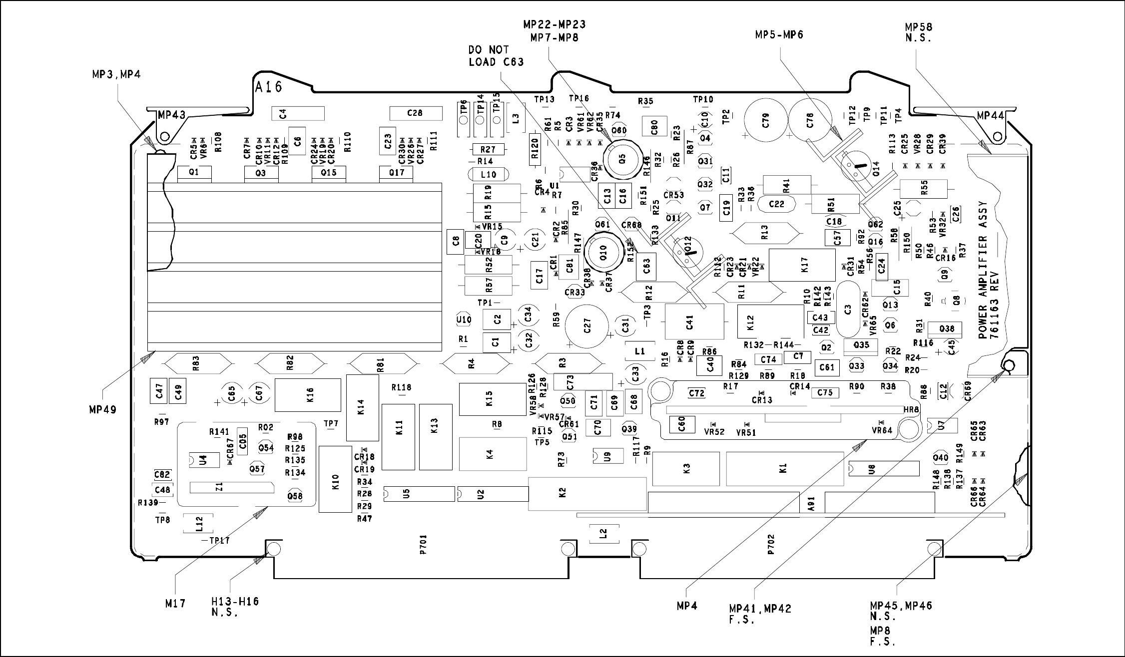
5700A/5720A Series II
Service Manual
7-84
Figure 7-22. A18 Filter/PA Supply PCA
5700A-7690

7
Schematic Diagrams
7-85
Figure 7-22. A18 Filter/PA Supply PCA (cont)
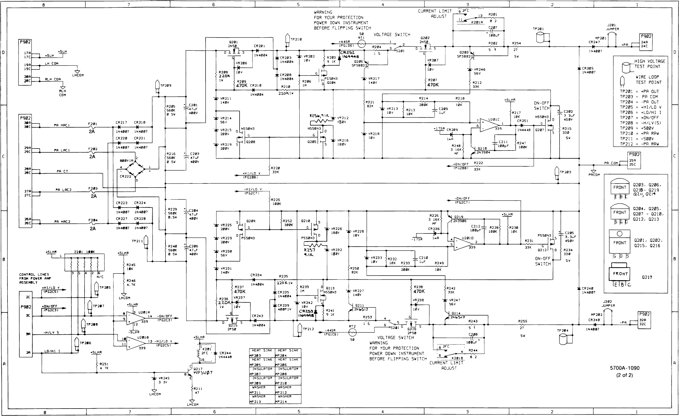
5700A/5720A Series II
Service Manual
7-86
Figure 7-22. A18 Filter/PA Supply PCA (cont)
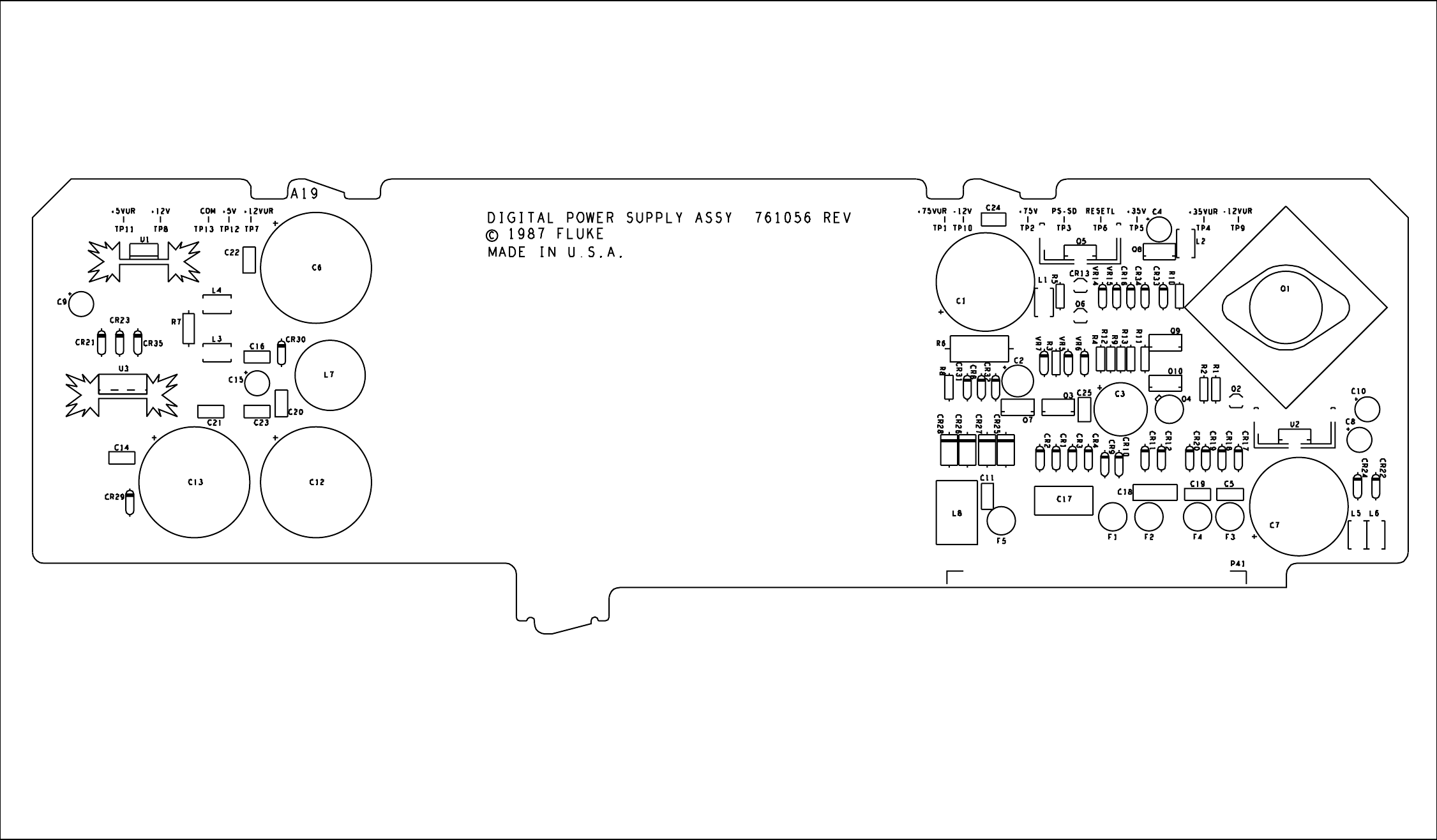
7
Schematic Diagrams
7-87
5700A-1604
Figure 7-23. A19 Digital Power Supply PCA
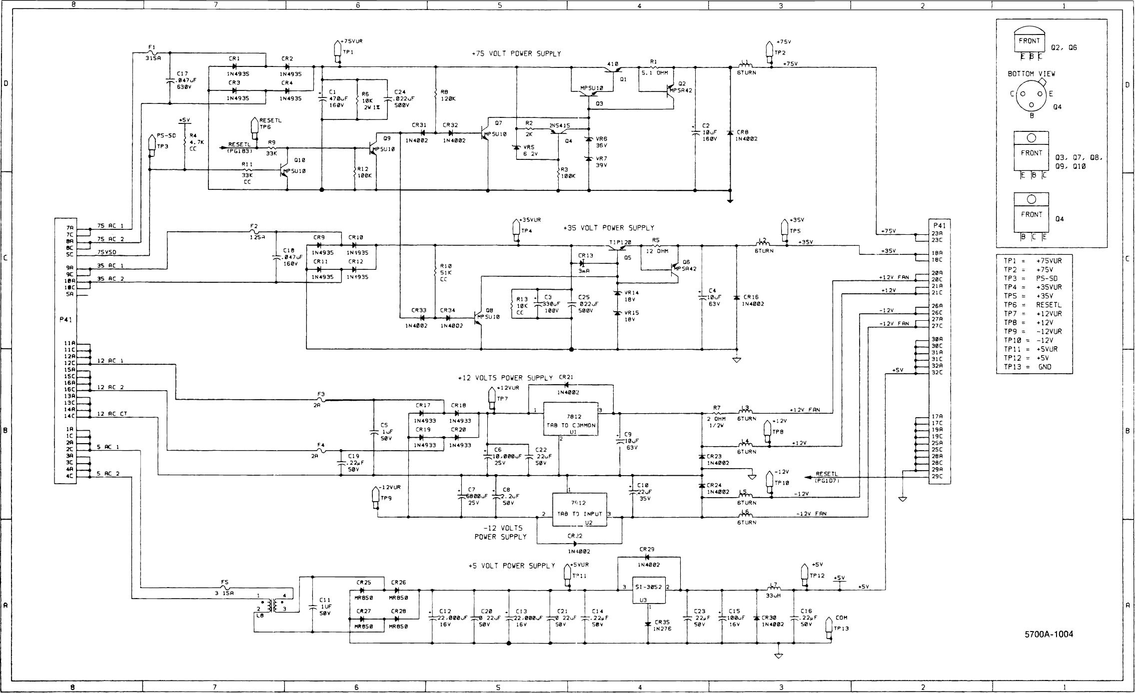
5700A/5720A Series II
Service Manual
7-88
Figure 7-23. A19 Digital Power Supply PCA (cont)
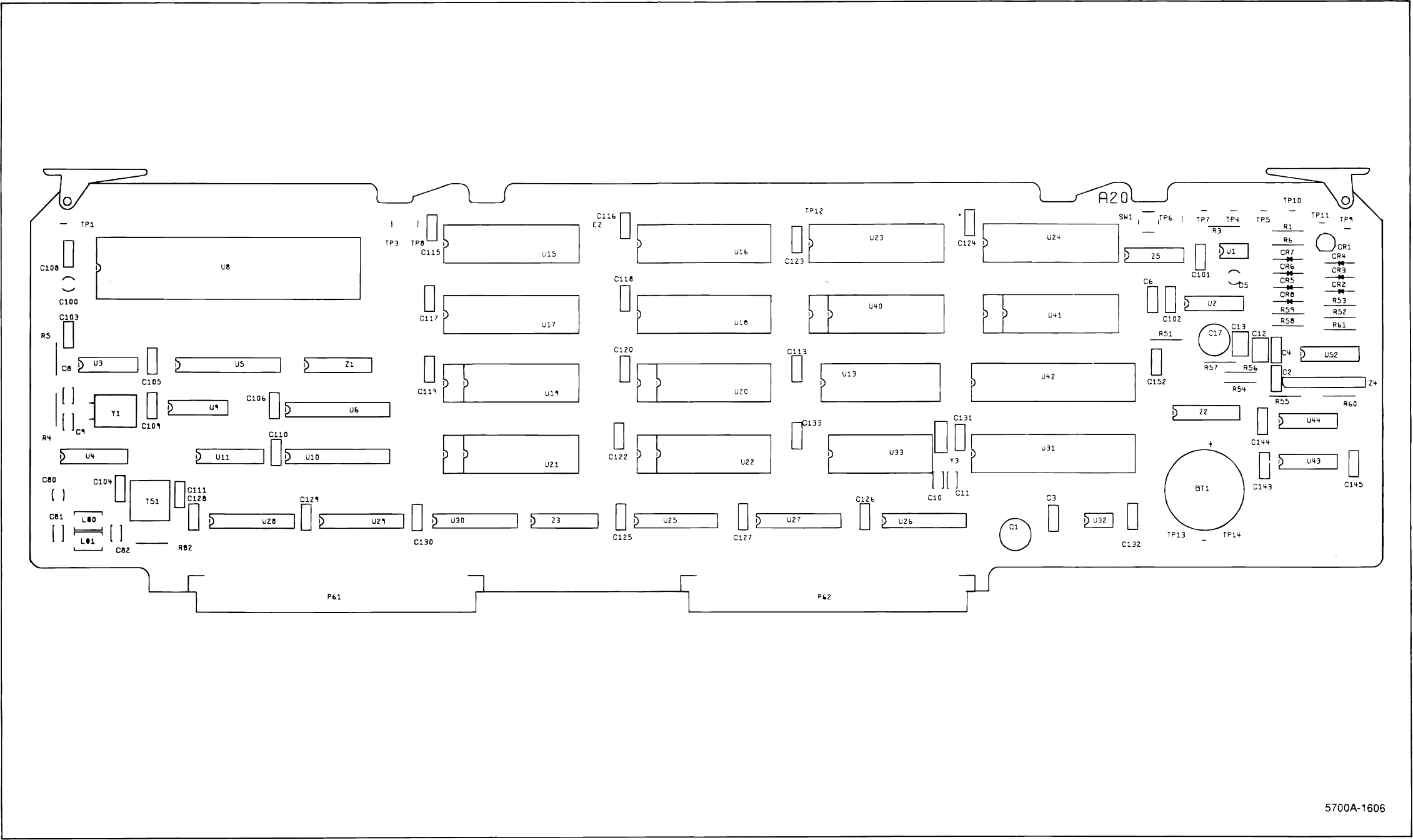
7
Schematic Diagrams
7-89
Figure 7-24. A20 CPU PCA
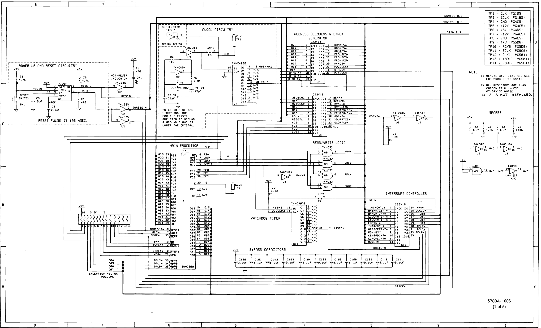
5700A/5720A Series II
Service Manual
7-90
Figure 7-24. A20 CPU PCA (cont)
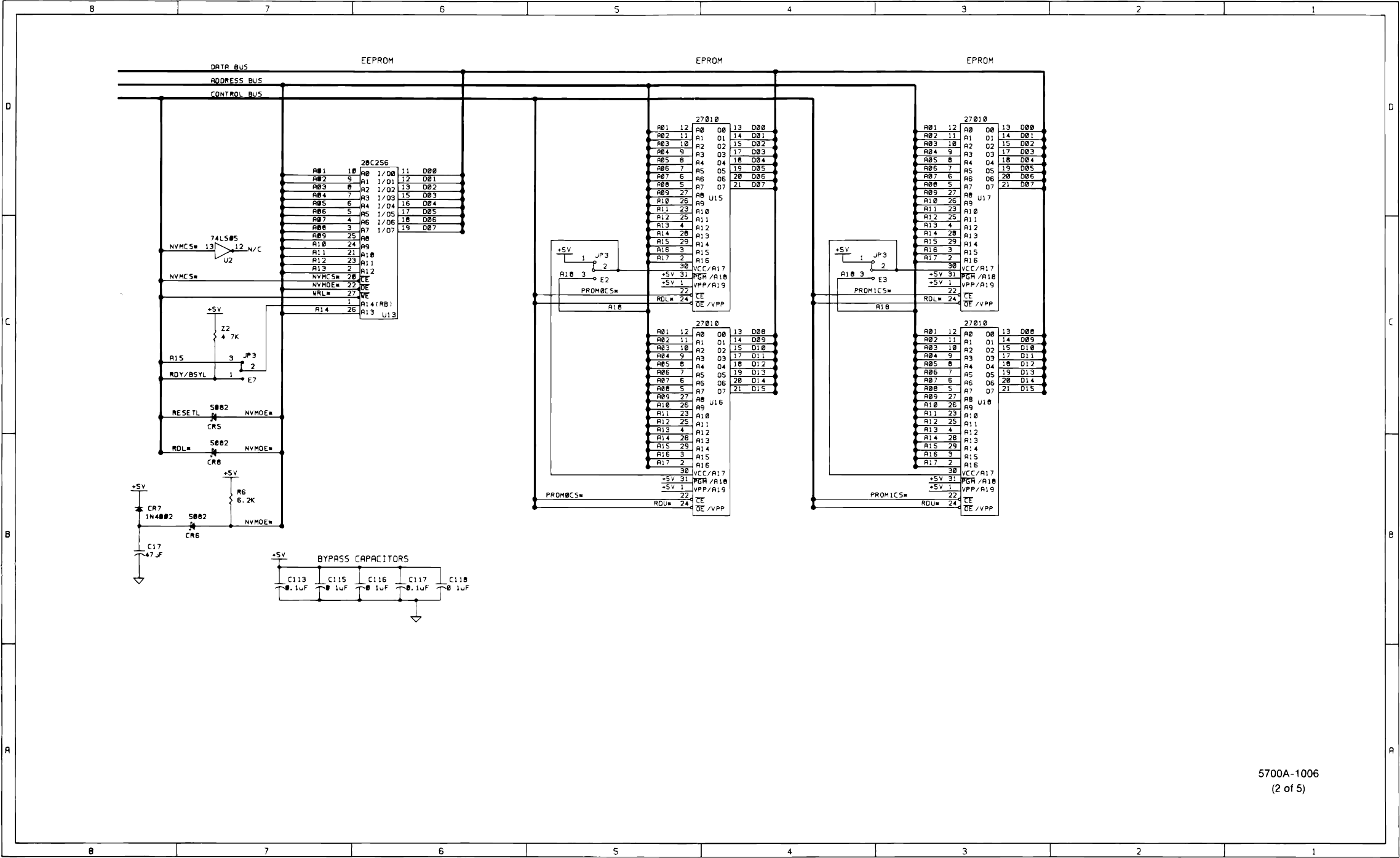
7
Schematic Diagrams
7-91
Figure 7-24. A20 CPU PCA (cont)
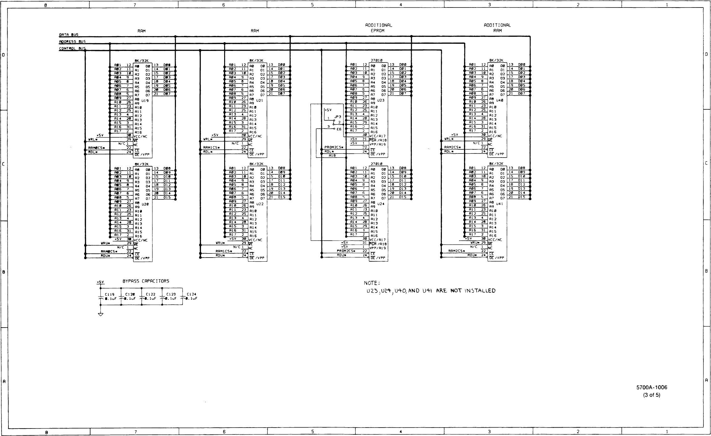
5700A/5720A Series II
Service Manual
7-92 Figure 7-24. A20 CPU PCA (cont)
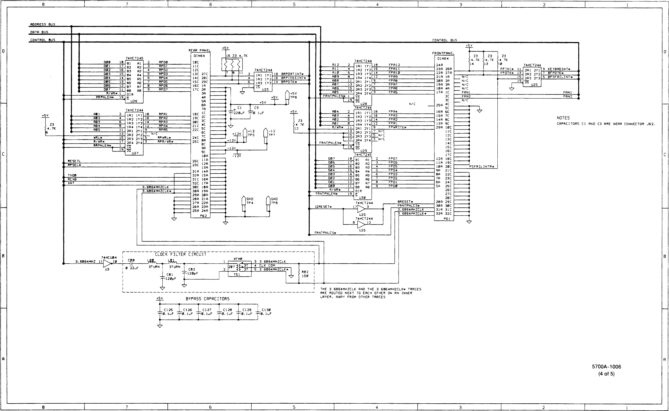
7
Schematic Diagrams
7-93
Figure 7-24. A20 CPU PCA (cont)
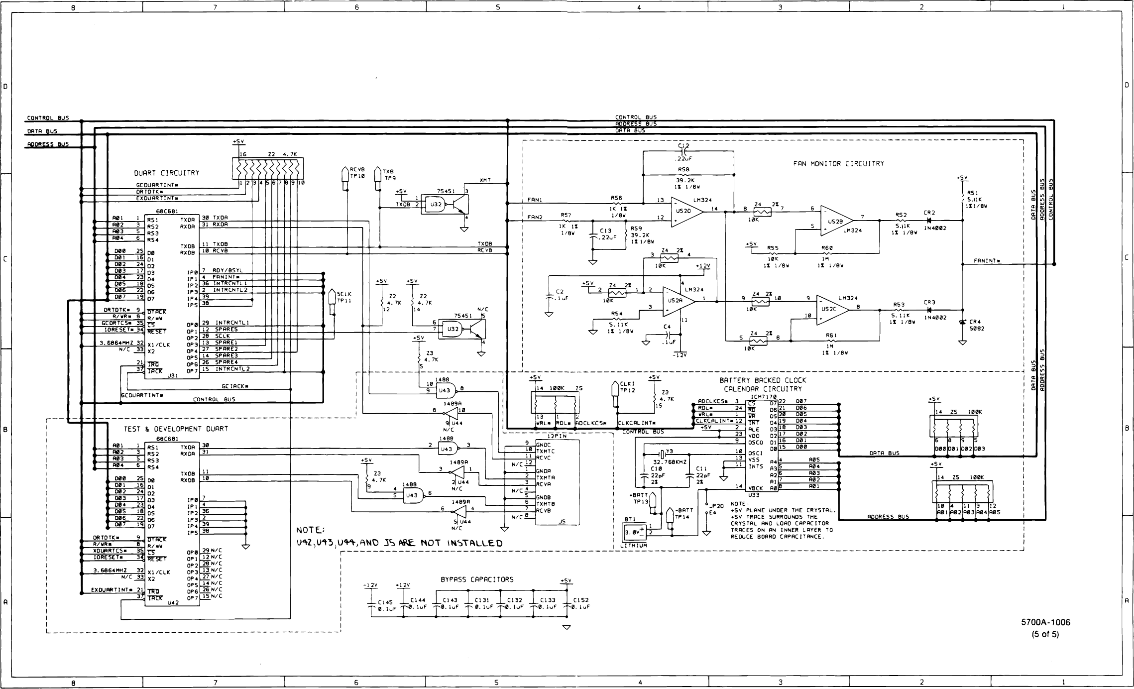
5700A/5720A Series II
Service Manual
7-94
Figure 7-24. A20 CPU PCA (cont)
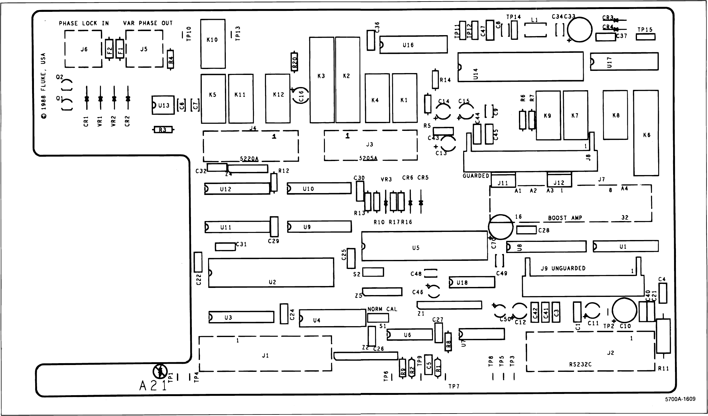
7
Schematic Diagrams
7-95
Figure 7-25. A21 Real Panel PCA
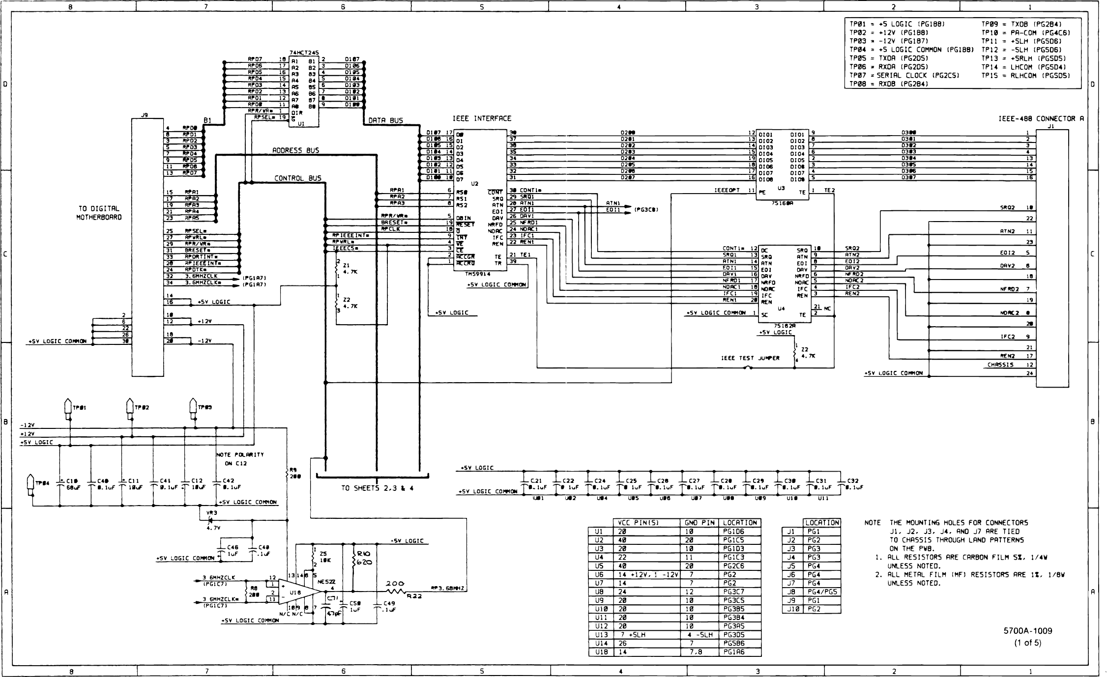
5700A/5720A Series II
Service Manual
7-96
Figure 7-25. A21 Rear Panel PCA (cont)
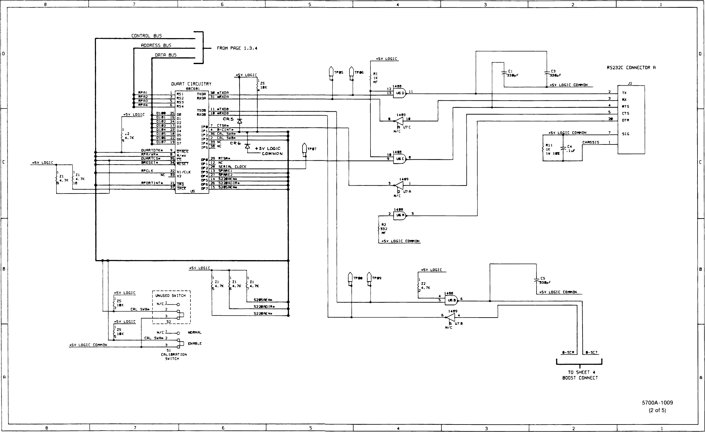
7
Schematic Diagrams
7-97
Figure 7-25. A21 Rear Panel PCA (cont)
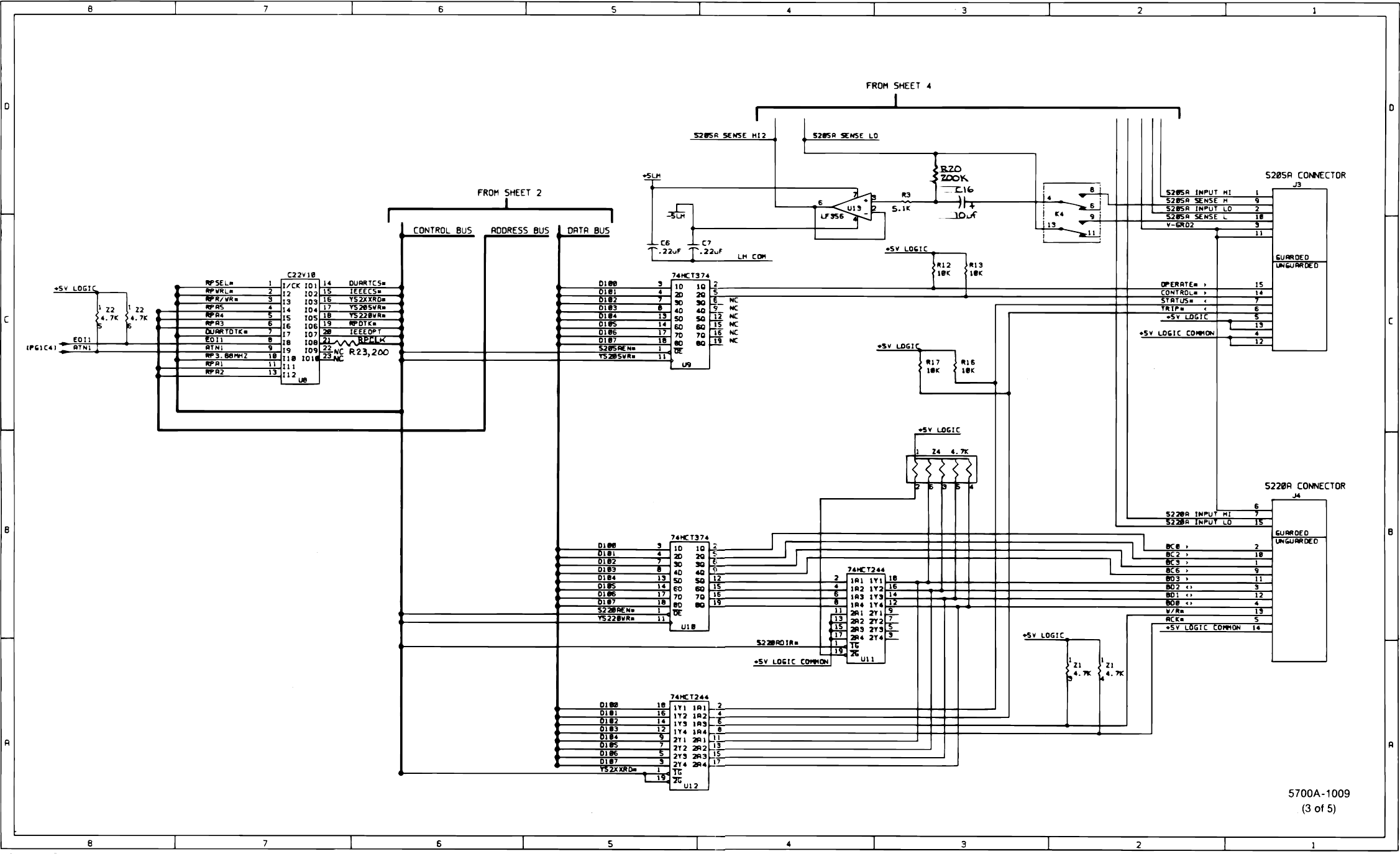
5700A/5720A Series II
Service Manual
7-98
Figure 7-25. A21 Rear Panel PCA (cont)
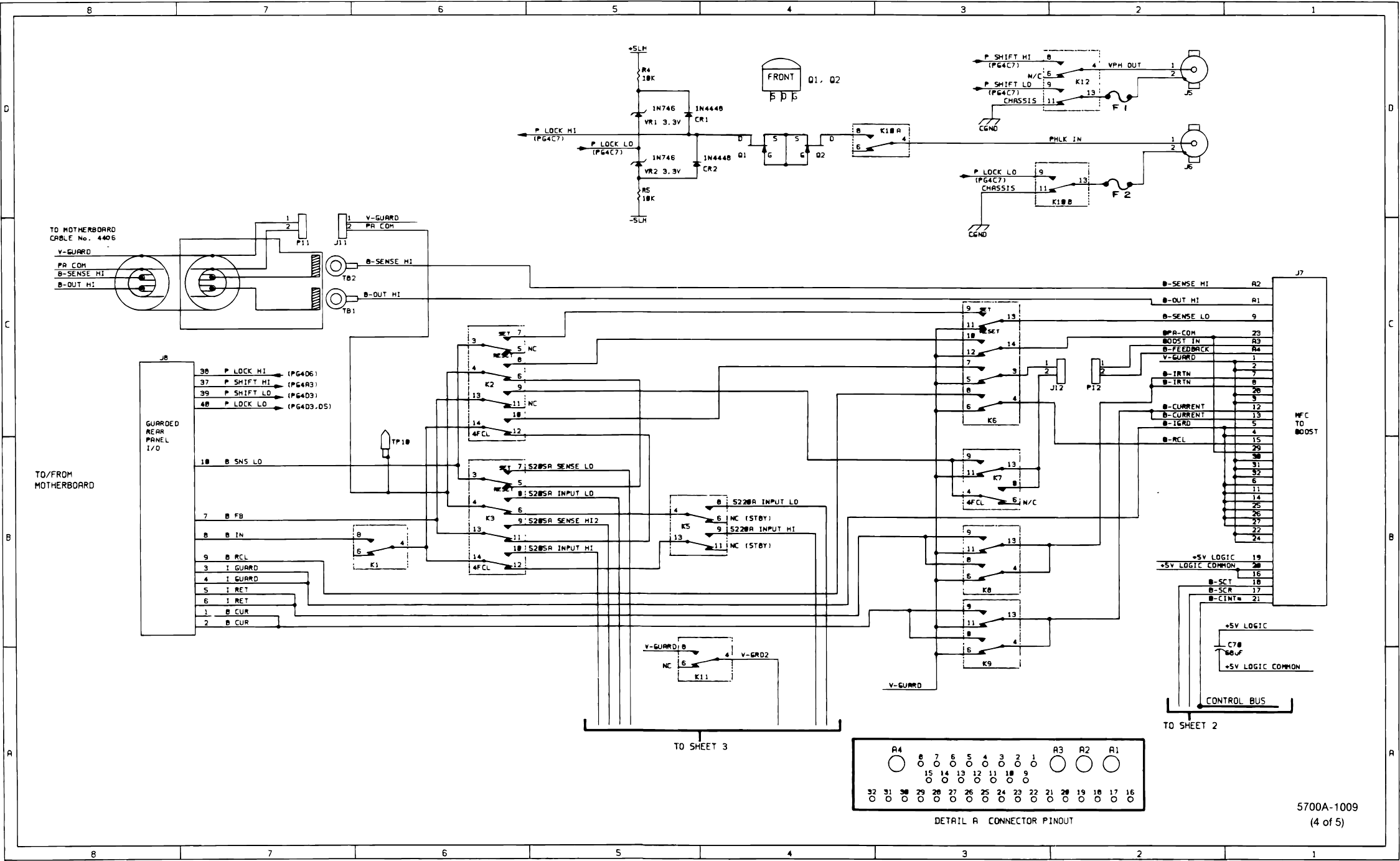
7
Schematic Diagrams
7-99
Figure 7-25. A21 Rear Panel PCA (cont)
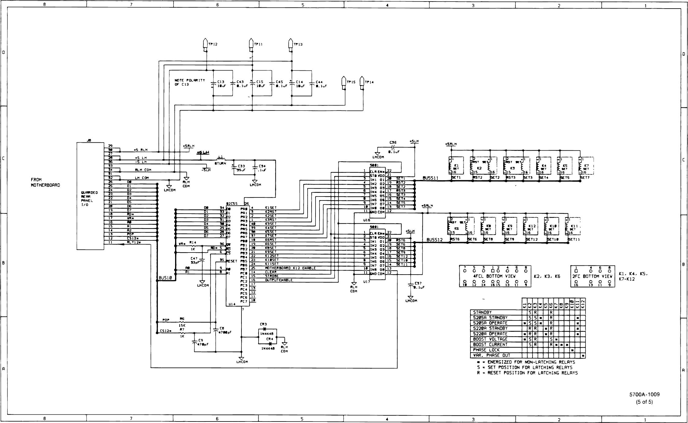
5700A/5720A Series II
Service Manual
7-100
Figure 7-25. A21 Rear Panel PCA (cont)
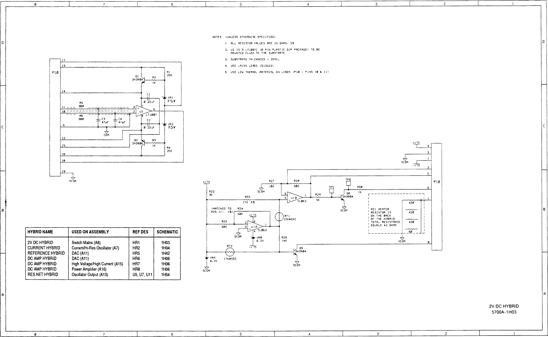
7
Schematic Diagrams
7-101
Figure 7-26. Hybrids
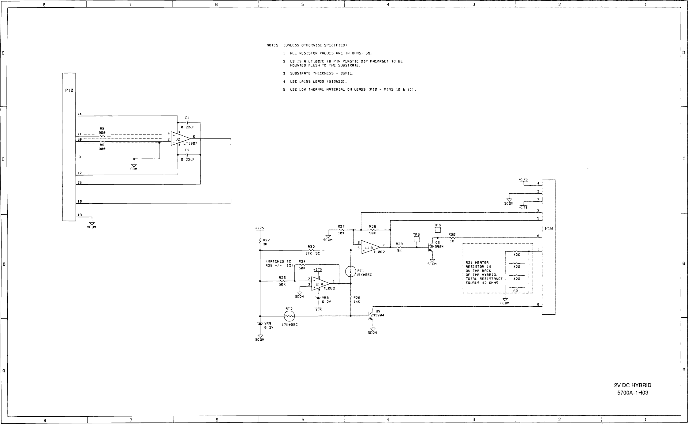
5700A/5720A Series II
Service Manual
7-102
Figure 7-26. Hybrids (cont)
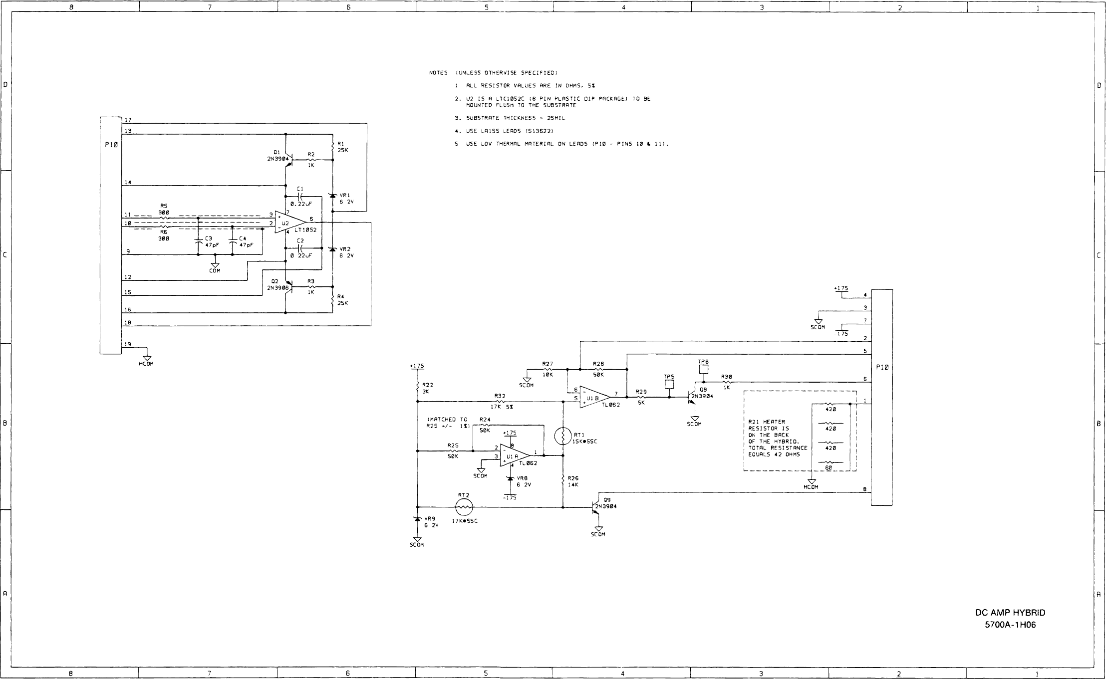
7
Schematic Diagrams
7-103
Figure 7-26. Hybrids (cont)
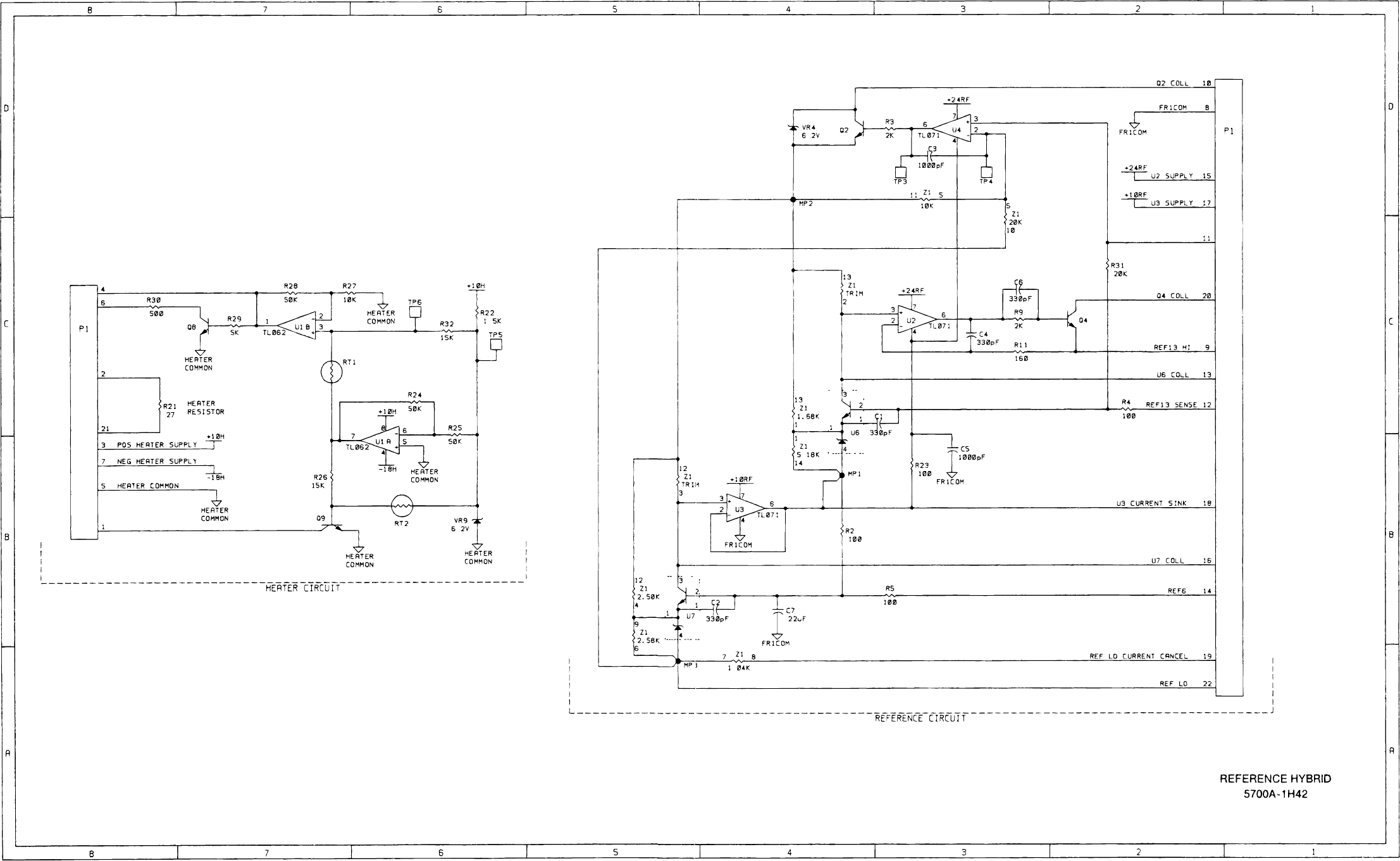
5700A/5720A Series II
Service Manual
7-104
Figure 7-26. Hybrids (cont)
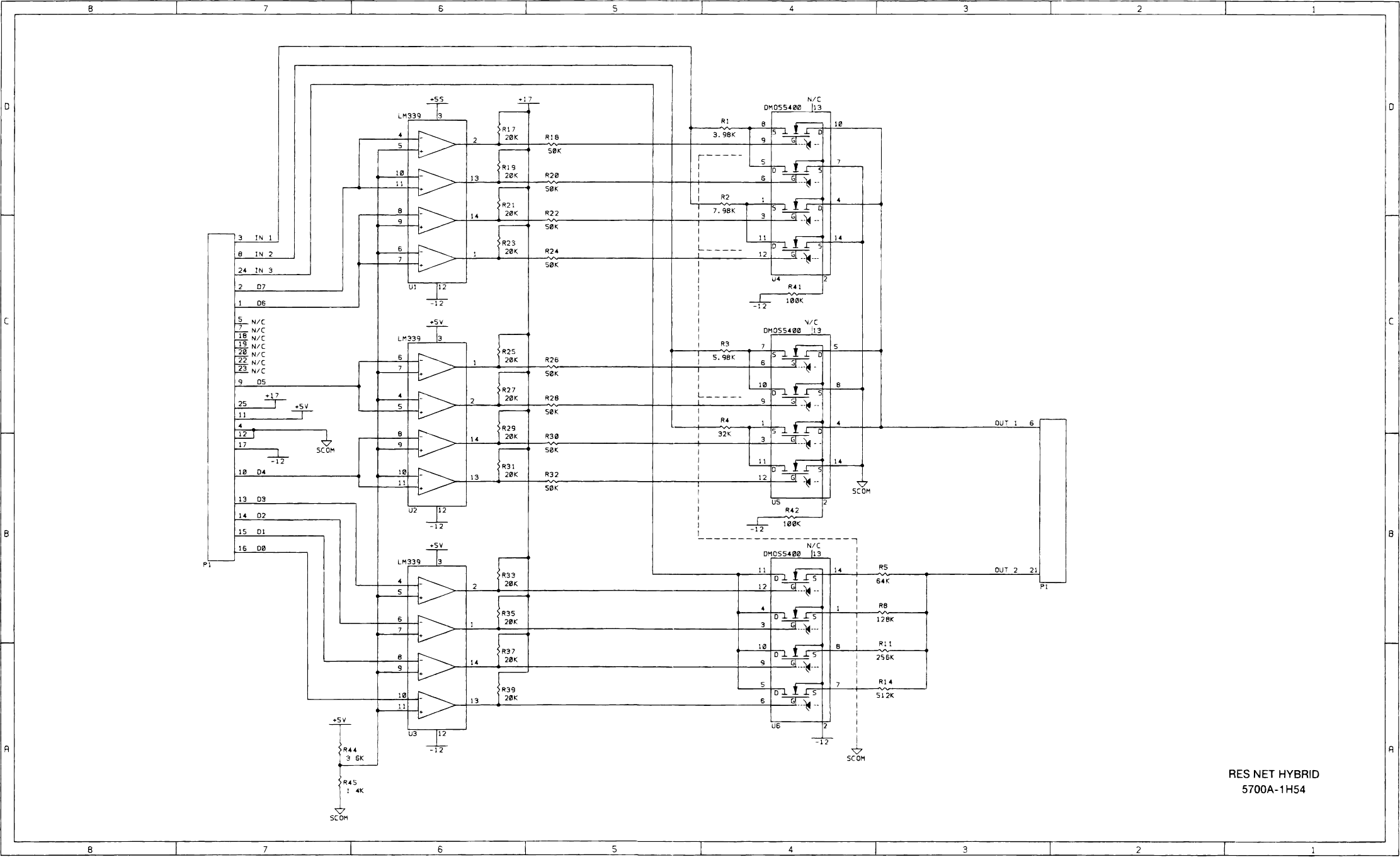
7
Schematic Diagrams
7-105
Figure 7-26. Hybrids (cont)

5700A/5720A Series II
Service Manual
7-106