Fuji Film 02100003 IEEE802.11 b/g/n Wireless LAN module User Manual module
Fuji Film Corporation IEEE802.11 b/g/n Wireless LAN module module
UserManual.wiki
>
Fuji Film
>
02100003 User Manual
>
User Manual (module)
Contents
1.
User Manual (module)
2.
User Manual (system)
User Manual (module)
Navigation menu
Upload a User Manual
Namespaces
Wiki Guide
HTML
PDF
Info
Views
User Manual
Discussion / Help
Navigation
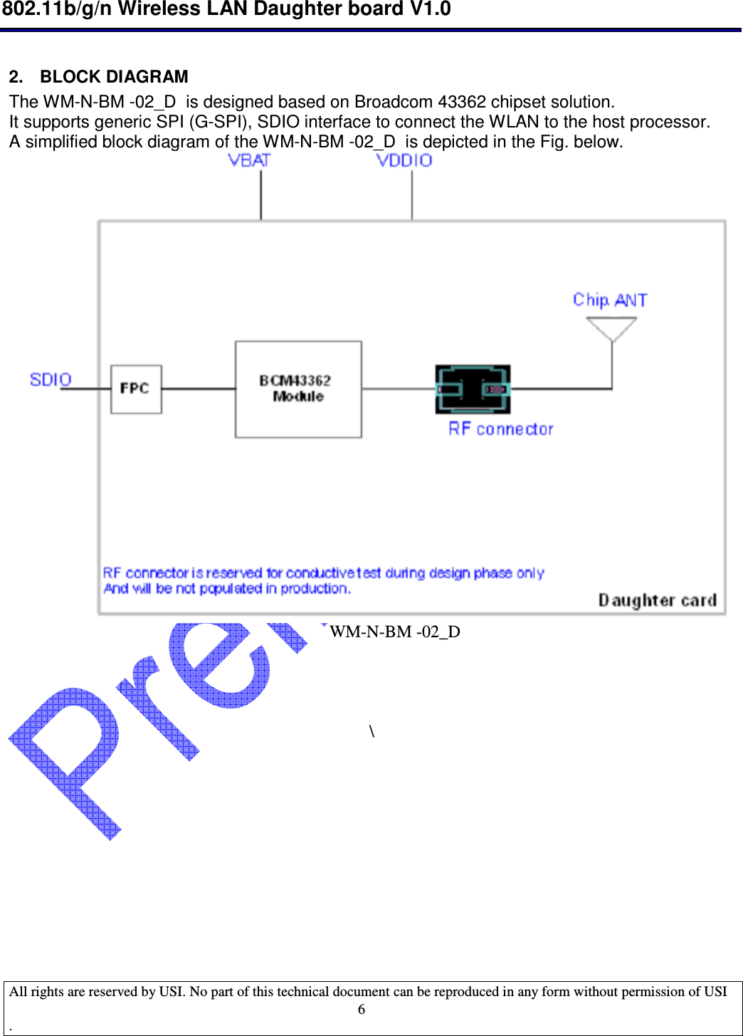
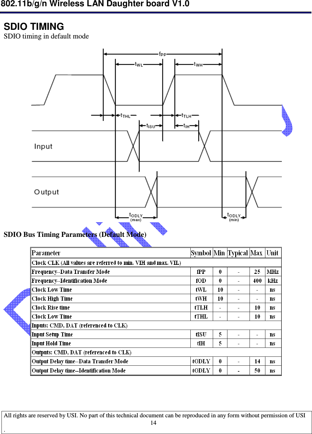
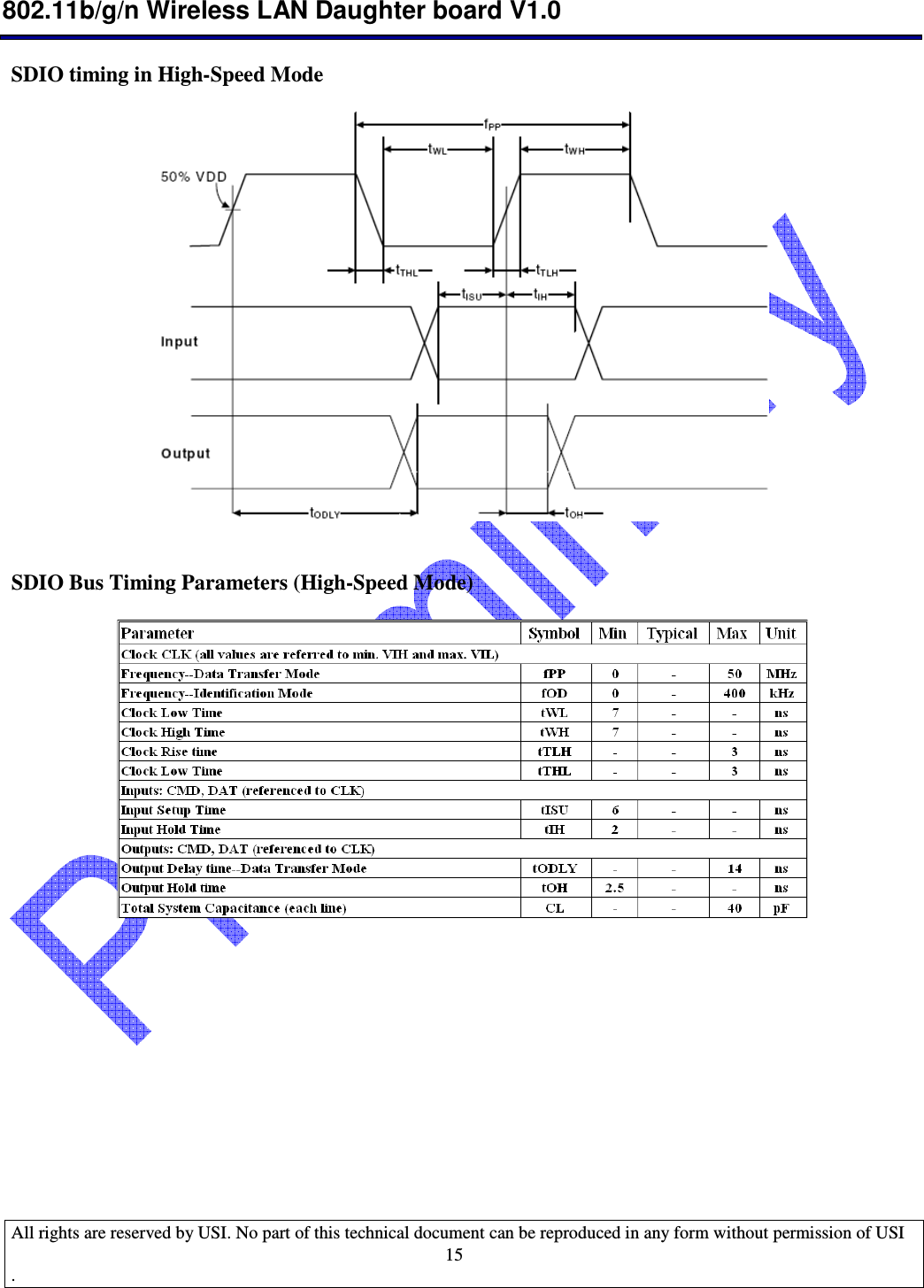
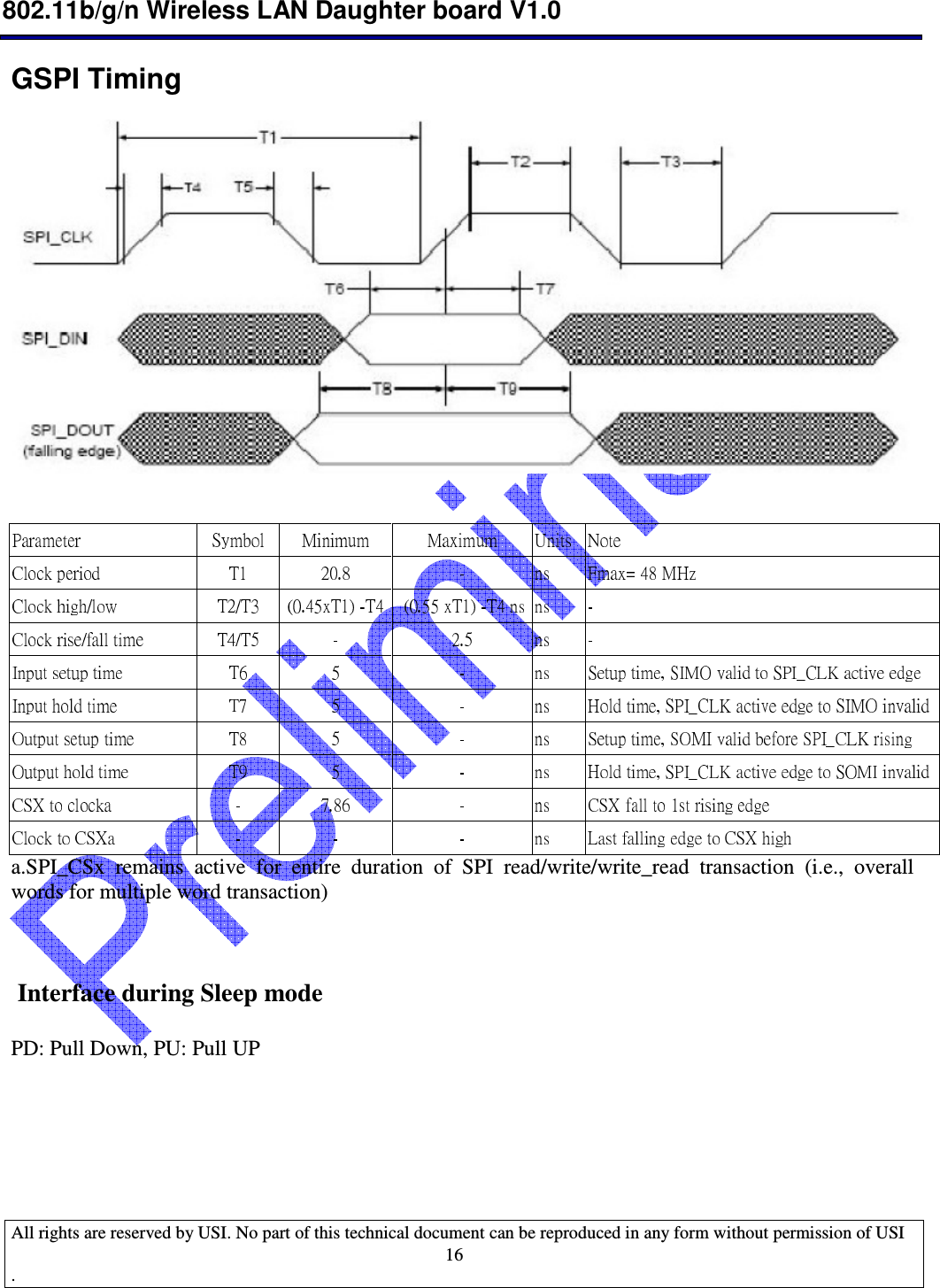
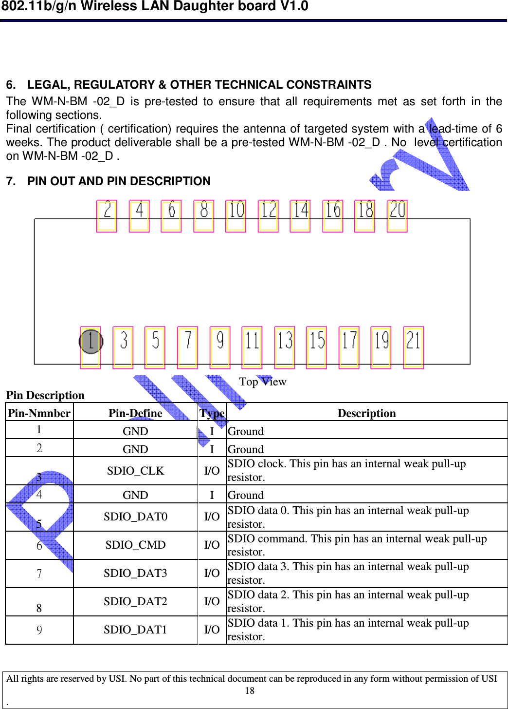
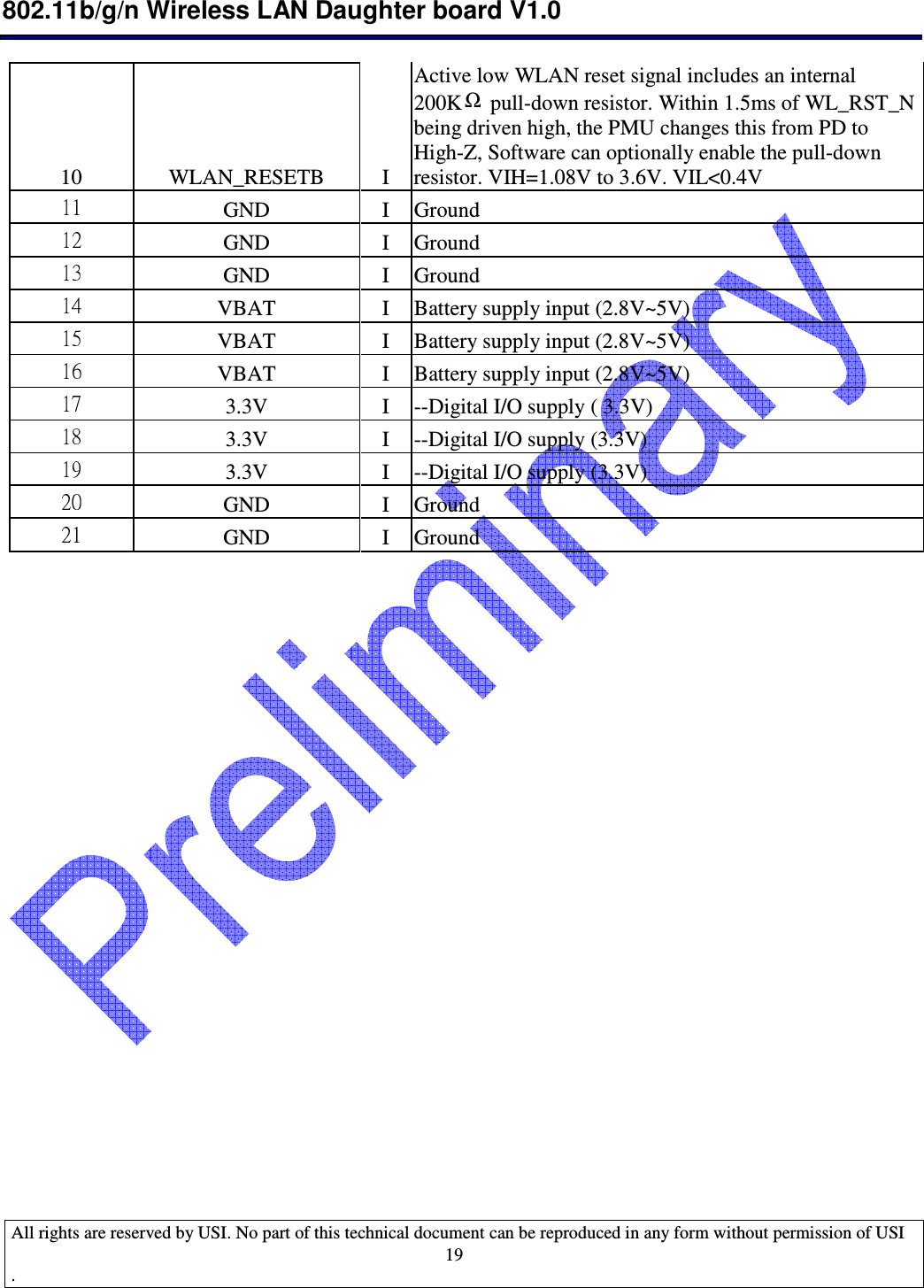
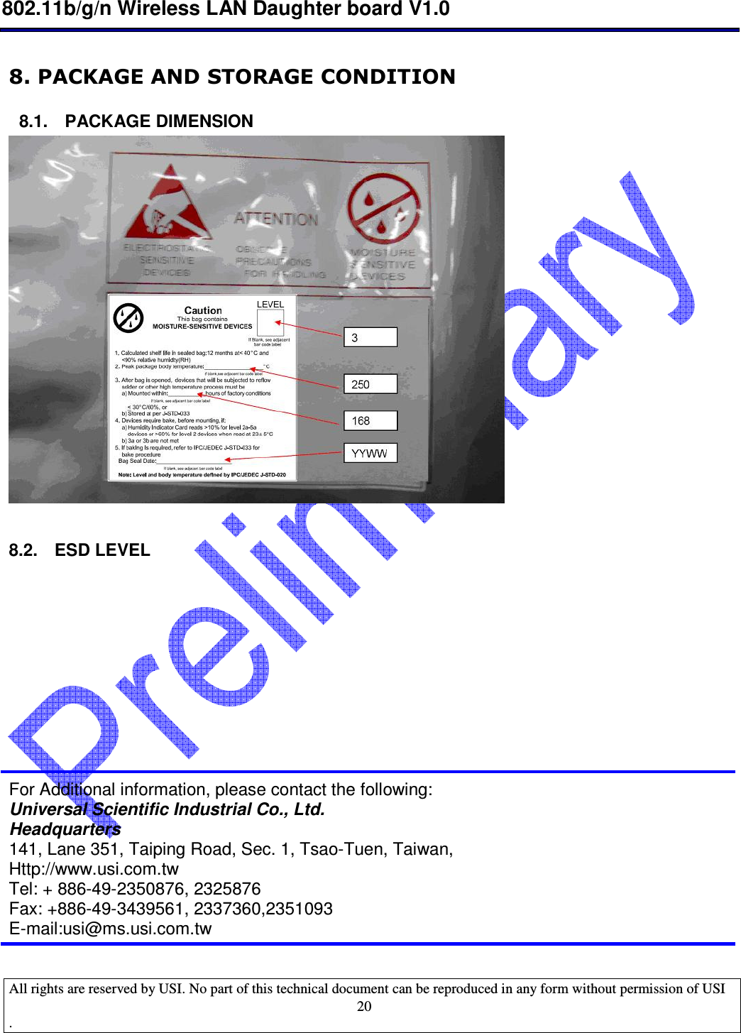
![[ ] All rights are reserved by USI. No part of this technical document can be reproduced in any form without permission of USI . 1 Data Sheet Of WM-N-BM -02_D WLAN Data Sheet Sep 7 2012 Rev 1.0 802.11b/g/n (WM-N-BM -02_D) www.usi.com.tw](https://usermanual.wiki/Fuji-Film/02100003.User-Manual-module/User-Guide-1921536-Page-1.png)