Fujitsu Mcj3230Ss Users Manual 01fcover
2015-01-25
: Fujitsu Fujitsu-Mcj3230Ss-Users-Manual-218449 fujitsu-mcj3230ss-users-manual-218449 fujitsu pdf
Open the PDF directly: View PDF ![]() .
.
Page Count: 161 [warning: Documents this large are best viewed by clicking the View PDF Link!]
- Front Cover
- FOR SAFE OPERATION
- Revision History
- Preface
- DISCLAIMER
- Important Alert Items
- REFERENCED STANDARDS
- Contents
- CHAPTER 1 General Description
- CHAPTER 2 Specifications
- CHAPTER 3 Installation Requirements
- CHAPTER 4 Host Interface
- 4.1 Interface Connector
- 4.2 Various Processes
- 4.3 SCSI Commands
- 4.3.1 TEST UNIT READY command
- 4.3.2 INQUIRY
- 4.3.3 READ CAPACITY command
- 4.3.4 MODE SELECT command
- 4.3.5 MODE SENSE command
- 4.3.6 START/STOP UNIT command
- 4.3.7 RESERVE command
- 4.3.8 RELEASE command
- 4.3.9 REQUEST SENSE command
- 4.3.10 PREVENT/ALLOW MEDIUM REMOVAL command
- 4.3.11 READ (6) command
- 4.3.12 READ (10) command
- 4.3.13 VERIFY command
- 4.3.14 WRITE (6) command
- 4.3.15 WRITE (10) command
- 4.3.16 WRITE AND VERIFY
- 4.3.17 SEEK (6) command
- 4.3.18 SEEK (10) command
- 4.3.19 ERASE command
- 4.3.20 SYNCHRONIZE CACHE command
- 4.3.21 FORMAT UNIT command
- 4.3.22 READ DEFECT DATA command
- 4.3.23 SEND DIAGNOSTIC command
- 4.3.24 RECEIVE DIAGNOSTIC RESULTS command
- 4.3.25 WRITE BUFFER command
- 4.3.26 READ LONG command
- 4.3.27 WRITE LONG command
- 4.4 SCSI Messages
- 4.5 Timing Rule
- CHAPTER 5 Operation and Cleaning
- CHAPTER 6 Diagnosis and Maintenance
- Glossary
- Acronyms and Abbreviations
- Index
- READER’S COMMENT FORM
- Back Cover

C156-E224-01EN
MCJ3230SS
OPTICAL DISK DRIVE
PRODUCT MANUAL
C156-E224-01EN
FOR SAFE OPERATION
Handling of This Manual
This manual contains important information for using this product. Read thoroughly before using
the product. Use this product only after thoroughly reading and understanding especially the
section "Important Alert Items" in this manual. Keep this manual handy, and keep it carefully.
FUJITSU makes every effort to prevent users and bystanders from being injured or from suffering
damage to their property. Use the product according to this manual.
This product is designed and manufactured for use in standard applications such as office work,
personal devices and household appliances. This product is not intended for special uses (atomic
controls, aeronautic or space systems, mass transport vehicle operating controls, medical devices for
life support, or weapons firing controls) where particularly high reliability requirements exist,
where the pertinent levels of safety are not guaranteed, or where a failure or operational error could
threaten a life or cause a physical injury (hereafter referred to as "mission-critical" use). Customers
considering the use of these products for mission-critical applications must have safety-assurance
measures in place beforehand. Moreover, they are requested to consult our sales representative
before embarking on such specialized use.
First Edition November 2001
The contents of this manual may be revised without prior notice.
The contents of this manual shall not be disclosed in any way or reproduced in any media without
the express written permission of Fujitsu Limited.
All Rights Reserved, Copyright FUJITSU LIMITED 2001

C156-E224-01EN
Revision History
(1/1)
Edition Date Revised section (*1)
(Added/Deleted/Altered) Details
01 November,
2001
——
*1 Section(s) with asterisk (*) refer to the previous edition when those were deleted.
This page is intentionally left blank.

C156-E224-01EN i
Preface
This manual describes the MCJ3230SS 90 mm (3.5-inch) optical disk drive.
This manual provides an overview of the above optical disk drives, and explains
their specifications, the requirements and procedures for installing them in a
system, and how to clean them.
The manual is intended for users who have a basic understanding of optical disk
drives and their use in computer systems.
See "Manual Organization" for details of the organization of manuals related to
optical disk drives and the scope of this manual. Use the other manuals shown in
"Manual Organization" together with this manual when necessary.
The organization of this manual, related reference manual and conventions for
alert messages follow.
Overview of Manual
This manual consists of the following six chapters, glossary, and abbreviation:
Chapter 1 General Description
This chapter introduces the MCJ3230SS optical disk drive and describes its
features, drive configuration, and system configuration.
Chapter 2 Specifications
This chapter describes the specifications of the MCJ3230SS optical disk drive and
the specifications of optical disk cartridges.
Chapter 3 Installation Requirements
This chapter describes the basic environmental, mounting, power supply, and
connection requirements for installing the MCJ3230SS optical disk drive in a user
system.
Chapter 4 Host Interface
This chapter describes the host interface of the MCJ3230SS optical disk drive.
Chapter 5 Diagnostics and Maintenance
This chapter describes how to operate and clean the MCJ3230SS optical disk
drive. This chapter also describes how to operate and clean optical disk cartridges.
Chapter 6 Diagnostics and Maintenance
This chapter describes the self-diagnostics functions and maintenance of the
MCJ3230SS optical disk drive.

Preface
ii C156-E224-01EN
Glossary
The glossary describes the technical terms that need to be understood to read this
manual.
Acronyms and Abbreviations
This manual contains a list of the abbreviations used in this manual and their
meanings.
CONVENTIONS USED IN THIS MANUAL
Throughout this manual, the MCJ3230SS optical disk drive are described as an
"ODD," "drive," "unit," "target (TARG)," or "device."
Decimal values are indicated without any modifiers added.
Hexadecimal values are indicated as X'17B9', 17B9h, 17B9H, and 17B9H.
Binary values are indicated as "010" and 010b.
Conventions for Alert Messages
This manual uses the following conventions to show the alert messages. An alert
message consists of an alert signal and alert statements. The alert signal consists
of an alert symbol and a signal word or just a signal word.
The following are the alert signals and their meanings:
This indicates a hazardous situation likely to result in
serious personal injury if the user does not perform
the procedure correctly.
This indicates a hazardous situation could result in
serious personal injury if the user does not perform
the procedure correctly.
This indicates a hazardous situation could result in
minor or moderate personal injury if the user does
not perform the procedure correctly. This alert signal
also indicates that damages to the product or other
property, may occur if the user does not perform the
product correctly.
This indicates information that could help the user
use the product more efficiently.
In the text, the alert signal is centered, followed below by the indented message.
A wider line space precedes and follows the alert message to show where the alert
message begins and ends. The following is an example:

Preface
C156-E224-01EN iii
(Example)
Low temperature burns: The surface temperatures of some ICs
on the printed circuit board unit in the optical disk drive exceed
55°C while operating. Be careful of low tenperature burns.
The main alert messages in the text are also listed in the “Important Alert Items.”
Attention
Please forward any comments you may have regarding this manual.
To make this manual easier for users to understand, opinions from readers are
needed. Please write your opinions or requests on the Comment at the back of this
manual and forward it to the address described in the sheet.

iv C156-E224-01EN
DISCLAIMER
Failure of the MCJ3230SS optical disk drive is defined as a failure requiring
adjustment, repair, or replacement. Fujitsu is not responsible for failure due to
misuse, operation outside the specified environment conditions, power line
trouble, controller problems, cable failure, or other failure not caused by the
optical disk drive itself.

C156-E224-01EN v
Important Alert Items
Important Alert Messages
The important alert messages in this manual are as follows:
A hazardous situation could result in minor or moderate personal
injury if the user does not perform the procedure correctly. Also,
damage to the product or other property, may occur if the user does not
perform the procedure correctly.
Task Alert message Page
Low temperature burns:
The surface temperatures of some ICs on the printed circuit
board unit in the optical disk drive exceed 55°C while
operating. Be careful of low tenperature burns.
3-1
Device damage:
1) Shock or vibration applied to the drive that exceeds the
values defined in the standard damage the drive. Use care
when unpacking.
2) Do not leave the drive in dirty or contaminated
environments.
3) Since static discharge may destroy the CMOS devices in
the drive, pay attention to the following points after
unpacking:
- Use an antistatic mat and wrist strap when handling
the drive.
- Hold the mounting frame when handling the drive.
Do not touch the Printed circuit board except when
setting the switches.
4) When handling the drive, hold both sides of the mounting
frame. When touching other than both sides of the
mounting frame, avoid putting force.
5) Do not forcibly push up the end of the header pin of the
printed circuit board unit when handling or setting the
drive.
3-21

Important Alert Items
vi C156-E224-01EN
Task Alert message Page
Device damage:
Be sure to turn on the power supply before inserting your
cartridge for the first time. It releases the device from
transport protection and enables you to insert the cartridge.
The device may be damaged if you insert the cartridge
without releasing the protection. From the next time, you
don't need to turn on the power supply beforehand.
Before moving the drive, remove the optical disk cartridge. If
the drive is moved with the optical disk cartridge loaded in it,
the head may move back and forth in the drive to damage the
head or disk and reading the data may fail.
3-22
•Make sure that the system power is off.
•Do not connect or disconnect any cable when the power is
on.
3-25
Device damage:
Before demounting the optical disk drive, turn off the system
power. Do not remove screws securing the cables and drive
when the power is on.
3-27
Device Damage:
Be sure to use the dedicated head cleaner described above.
5-6
Damage for data medium:
Do not use this cleaning kit for the floppy disk or the optical
disk cartridge used for other optical disk drive.
5-12
Damage for disk medium:
Clean the cartridge at clean place. Put a disposable groves at
cleaning so that the fingerprint does not put on the disk media
(recommendation).
5-12
Damage for disk medium:
At setting the cartridge to the setting case, do not apply the
heavy shock and push hardly.
5-13
Eye inflammation:
In case of contact with eyes, immediately flush eyes with
water.
5-14
Data loss:
In case of regular repair, the optical disk cartridge should not
be attached except where the cartridge causes the error. And
before having the drive repaired, save the data in the
cartridge. Fujitsu is not responsible for data lost during
maintenance or repair.
6-3

C156-E224-01EN vii
OPTICAL DISK DRIVE
PRODUCT MANUAL
(C156-E224)
<This manual>
1. GENERAL DESCRIPTION
2. SPECIFICATIONS
3. INSTALLATION REQUIREMENTS
4. HOST INTERFACE
5. OPERATION AND CLEANING
6. DIAGNOSTICS AND MAINTENANCE
OPTICAL DISK DRIVES
MAINTENANCE MANUAL
(C156-F043)
1. MAINTENANCE AND DIAGNOSIS
2. FAULT ANALYSIS
3. REMOVAL AND REPLACEMENT
PROCEDURES
4. PRINCIPLES OF OPERATION
5. CLEANING
MANUAL ORGANIZATION

viii C156-E224-01EN
REFERENCED STANDARDS
The product specifications and functions described in this manual conform to the
following standards:
Specification
(document) number
Name Concerned organization
ANSI X3. 131-1986 American National Standard for Information
Systems-Small Computer System Interface.
(SCSI)
American National
Standards Institute
(ANSI)
ANSI X3. 131-1994 American National Standard for Information
Systems-Small Computer System Interface-2.
(SCSI-2)
American National
Standards Institute
(ANSI)
ISO/IEC 10090 90mm Optical Disk Cartridges, rewritable and
read only, for data interchange.
ISO/IEC *1
ISO/IEC 13963 Data Interchange on 90mm Optical Disk
cartridges Capacity: 230 megabytes per
cartridges.
ISO/IEC *1
ISO/IEC 15041 Data Interchange on 90mm Optical Disk
Cartridges Capacity: 640 megabytes per
cartridges.
ISO/IEC JTC1 *1
Cherry Book GIGAMO 1.3GB 90mm Magneto-Optical Disk
System.
FUJITSU LIMITED
SONY CORPORATION
Cherry Book 2 GIGAMO 2.3GB 90mm Magneto-Optical Disk
System.
FUJITSU LIMITED
SONY CORPORATION
*1 ISO= International Organization for Standardization
IEC= International Electrical for Commission
JTC1= Joint Technical Committee 1

C156-E224-01EN ix
Contents
Preface .........................................................................................................i
DISCLAIMER .......................................................................................................iv
MANUAL ORGANIZATION ...................................................................................vii
CHAPTER 1 General Description.................................................................. 1-1
1.1 Features ........................................................................................................1-2
1.1.1 Performance ..........................................................................................1-2
1.1.2 Reliability ..............................................................................................1-3
1.1.3 Maintainability/operability....................................................................1-4
1.1.4 Adaptability...........................................................................................1-4
1.1.5 Interface.................................................................................................1-5
1.2 Drive Configuration......................................................................................1-7
1.2.1 Drive model...........................................................................................1-7
1.2.2 Configuration ........................................................................................1-8
1.2.3 Mechanical sections ..............................................................................1-9
1.2.4 Control circuit section .........................................................................1-10
CHAPTER 2 Specifications............................................................................ 2-1
2.1 Optical Disk Drive Specifications ................................................................2-1
2.1.1 Model and product number ...................................................................2-1
2.1.2 Drive specifications...............................................................................2-2
2.1.3 Environmental and power requirements................................................2-4
2.1.4 Error rate ...............................................................................................2-6
2.1.5 Reliability ..............................................................................................2-6
2.2 Optical Disk Cartridge Specifications ..........................................................2-7
2.2.1 Recommended optical disk cartridge specifications .............................2-7
2.2.2 Optical disk cartridge ............................................................................2-8
2.2.3 Disk specifications ................................................................................2-9

Contents
x C156-E224-01EN
2.3 Defect Management....................................................................................2-11
2.3.1 Defect management schematic diagram ..............................................2-11
CHAPTER 3 Installation Requirements.........................................................3-1
3.1 Environmental Requirements .......................................................................3-1
3.1.1 Temperature measurement point ...........................................................3-1
3.1.2 Temperature requirements and measuring method................................3-3
3.1.3 Air flow .................................................................................................3-3
3.1.4 Temperature rise under several conditions ............................................3-4
3.1.5 Air purity ...............................................................................................3-4
3.2 Mounting Requirements ...............................................................................3-5
3.2.1 External dimensions ..............................................................................3-5
3.2.2 Installation direction ..............................................................................3-7
3.2.3 Centers of gravity ..................................................................................3-8
3.2.4 Notes on mounting.................................................................................3-9
3.3 Power Supply Requirements.......................................................................3-11
3.4 Cable Connections ......................................................................................3-12
3.4.1 Drive connectors..................................................................................3-12
3.4.2 Cable connector specifications ............................................................3-15
3.4.3 Connection Modes...............................................................................3-16
3.5 Settings .......................................................................................................3-18
3.5.1 Default jumper settings........................................................................3-18
3.5.2 Setting terminal....................................................................................3-18
3.6 Notes on Drive Handling ............................................................................3-21
3.7 Mounting.....................................................................................................3-24
3.7.1 Checks before mounting the drive.......................................................3-24
3.7.2 Mounting procedure ............................................................................3-24
3.8 Cable Connections ......................................................................................3-25
3.9 Operation Confirmation and Preparation for Use after Installation............3-26
3.9.1 Confirming initial operations...............................................................3-26
3.9.2 Connection check ................................................................................3-27
3.10 Dismounting Drive .....................................................................................3-27

C156-E224-01EN xi
CHAPTER 4 Host Interface ............................................................................ 4-1
4.1 Interface Connector ......................................................................................4-1
4.2 Various Processes.........................................................................................4-4
4.2.1 Reset response .......................................................................................4-4
4.2.2 Defective sector management ...............................................................4-4
4.2.3 Automatic alternate sector assignment function....................................4-4
4.2.4 Cache function.......................................................................................4-5
4.2.4.1 Data buffer ....................................................................................4-5
4.2.4.2 Read cache ....................................................................................4-5
4.2.4.3 MO write cache.............................................................................4-6
4.2.5 Power management function .................................................................4-6
4.2.6 Power mode...........................................................................................4-6
4.2.6.1 Active mode ..................................................................................4-7
4.2.6.2 Pre-idle mode ................................................................................4-7
4.2.6.3 Idle mode.......................................................................................4-7
4.2.6.4 Standby mode................................................................................4-7
4.2.6.5 Standby timer ................................................................................4-7
4.2.6.6 Power mode transition...................................................................4-8
4.2.7 LED indications.....................................................................................4-9
4.3 SCSI Commands ........................................................................................4-10
4.3.1 TEST UNIT READY command .........................................................4-11
4.3.2 INQUIRY ............................................................................................4-11
4.3.3 READ CAPACITY command ............................................................4-13
4.3.4 MODE SELECT command.................................................................4-13
4.3.5 MODE SENSE command ...................................................................4-22
4.3.6 START/STOP UNIT command ..........................................................4-24
4.3.7 RESERVE command ..........................................................................4-25
4.3.8 RELEASE command...........................................................................4-26
4.3.9 REQUEST SENSE command .............................................................4-26
4.3.10 PREVENT/ALLOW MEDIUM REMOVAL command ....................4-31
4.3.11 READ (6) command............................................................................4-32
4.3.12 READ (10) command..........................................................................4-32
4.3.13 VERIFY command..............................................................................4-33
4.3.14 WRITE (6) command..........................................................................4-33
4.3.15 WRITE (10) command........................................................................4-34
4.3.16 WRITE AND VERIFY .......................................................................4-34
4.3.17 SEEK (6) command.............................................................................4-35
4.3.18 SEEK (10) command...........................................................................4-35
4.3.19 ERASE command ...............................................................................4-36
4.3.20 SYNCHRONIZE CACHE command .................................................4-36

Contents
xii C156-E224-01EN
4.3.21 FORMAT UNIT command .................................................................4-37
4.3.22 READ DEFECT DATA command .....................................................4-38
4.3.23 SEND DIAGNOSTIC command.........................................................4-39
4.3.24 RECEIVE DIAGNOSTIC RESULTS command................................4-39
4.3.25 WRITE BUFFER command................................................................4-40
4.3.26 READ LONG command .....................................................................4-41
4.3.27 WRITE LONG command....................................................................4-41
4.4 SCSI Messages ...........................................................................................4-42
4.4.1 Message formats..................................................................................4-42
4.4.2 Message types......................................................................................4-42
4.4.3 Message functions ...............................................................................4-43
4.5 Timing Rule ................................................................................................4-46
CHAPTER 5 Operation and Cleaning ............................................................5-1
5.1 Operating Optical Disk Drive .......................................................................5-1
5.1.1 Optical disk drive...................................................................................5-2
5.1.2 Note .......................................................................................................5-3
5.1.3 Inserting cartridge..................................................................................5-3
5.1.4 Ejecting (removing) cartridge................................................................5-5
5.2 Cleaning Drive..............................................................................................5-6
5.3 Optical Disk Cartridge Operation .................................................................5-7
5.3.1 Optical disk cartridge.............................................................................5-7
5.3.2 Write protect tab ....................................................................................5-8
5.3.3 How to affix an index label on the MO cartridge..................................5-9
5.3.4 Notes......................................................................................................5-9
5.4 Cleaning Optical Disk Cartridge.................................................................5-11
5.4.1 Cleaning tool .......................................................................................5-11
5.4.2 Cleaning procedure..............................................................................5-12
CHAPTER 6 Diagnosis and Maintenance .....................................................6-1
6.1 Diagnosis ......................................................................................................6-1
6.1.1 Initial self-diagnosis ..............................................................................6-1
6.1.2 Diagnostic command .............................................................................6-2
6.1.3 Test program..........................................................................................6-2

C156-E224-01EN xiii
6.2 Maintenance Information .............................................................................6-3
6.2.1 Maintenance requirements ....................................................................6-3
6.2.2 Revision number ...................................................................................6-4
Glossary ……………………………………………………………………….GL-1
Abbreviations …….…………………………………………………………………AB-1
Index ………………………………………………………………………...IN-1

Contents
xiv C156-E224-01EN
Illustrations
Figures
Figure 1.1 Outer view (with panel) .....................................................................................1-7
Figure 1.2 Outer view (without panel) ................................................................................1-7
Figure 1.3 Optical disk drive configuration ........................................................................1-8
Figure 1.4 Control circuit section block diagram..............................................................1-10
Figure 2.1 Optical disk cartridge.........................................................................................2-8
Figure 2.2 Algorithms for alternate processing.................................................................2-11
Figure 2.3 Example of alternate processing ......................................................................2-12
Figure 3.1 Surface temperature measurement points ..........................................................3-2
Figure 3.2 Dimensions ........................................................................................................3-5
Figure 3.3 Dimensions (without panel)...............................................................................3-6
Figure 3.4 Installation directions.........................................................................................3-7
Figure 3.5 Centers of gravity...............................................................................................3-8
Figure 3.6 Mounting frame structure ..................................................................................3-9
Figure 3.7 Service clearance .............................................................................................3-10
Figure 3.8 Current waveform (+5 VDC)...........................................................................3-11
Figure 3.9 Connector and terminal locations ....................................................................3-12
Figure 3.10 Location of setting terminal.............................................................................3-12
Figure 3.11 Shape of setting terminal .................................................................................3-13
Figure 3.12 SCSI bus connection modes ............................................................................3-16
Figure 3.13 SCSI bus connecti on modes ...........................................................................3-17
Figure 3.14 Setting terminal (CNH2) .................................................................................3-18
Figure 3.15 Packing style....................................................................................................3-23
Figure 4.1 SCSI interface connector (ODD side)................................................................4-1
Figure 4.2 SCSI interface connector (cable side)................................................................4-2
Figure 4.3 Power mode .......................................................................................................4-8
Figure 4.4 BUS FREE phase.............................................................................................4-49
Figure 4.5 ARBITRATION phase ....................................................................................4-50
Figure 4.6 SELECTION phase..........................................................................................4-51
Figure 4.7 RESELECTION phase.....................................................................................4-51
Figure 4.8 Transfer in asynchronous mode .......................................................................4-52
Figure 4.9 Transfer in FAST SCSI mode..........................................................................4-53
Figure 4.10 ATTENTION condition...................................................................................4-54
Figure 5.1 Optical disk drive front view (with panel).........................................................5-2
Figure 5.2 Inserting cartridge ..............................................................................................5-4
Figure 5.3 Removing cartridge............................................................................................5-5
Figure 5.4 Optial disk cartridge...........................................................................................5-7
Figure 5.5 Write protect tab ................................................................................................5-8
Figure 5.6 How to stick an index label on the MO cartridge ..............................................5-9
Figure 5.7 Cleaning procedure (1) ....................................................................................5-12
Figure 5.8 Cleaning procedure (2) ....................................................................................5-13
Figure 5.9 Cleaning procedure (3) ....................................................................................5-13
Figure 5.10 Cleaning procedure (4) ....................................................................................5-14

C156-E224-01EN xv
Figure 6.1 Revision label ....................................................................................................6-4
Figure 6.2 Revision number indication...............................................................................6-4

Contents
xvi C156-E224-01EN
Tables
Table 2.1 Model and order number....................................................................................2-1
Table 2.2 Specifications (1 of 2)........................................................................................2-2
Table 2.2 Specifications (2 of 2)........................................................................................2-3
Table 2.3 Environmental and power requirements (1 of 2) ...............................................2-4
Table 2.3 Environmental and power requirements (2 of 2) ...............................................2-5
Table 2.4 Power consumption in power save mode
when the temperature inside the drive is 20°C or lower ....................................2-5
Table 2.5 Recommended optical disk cartridge specifications..........................................2-7
Table 2.6 Disk specifications...........................................................................................2-10
Table 3.1 Temperature requirements at measurement points ............................................3-3
Table 3.2 Temperature at each measuring point (Reference) ............................................3-4
Table 3.3 Pin assignments................................................................................................3-14
Table 3.4 Recommended components for connection .....................................................3-15
Table 3.5 SCSI ID setting (CNH2) ..................................................................................3-18
Table 3.6 SCSI terminating resistor mode.......................................................................3-19
Table 3.7 Write cache mode setting.................................................................................3-19
Table 3.8 Spindle motor automatic stop mode setting.....................................................3-20
Table 4.1 SCSI interface connector pin assignments (single-ended type).........................4-3
Table 4.2 LED indications .................................................................................................4-9
Table 4.3 SCSI commands...............................................................................................4-10
Table 4.4 TEST UNIT READY command......................................................................4-11
Table 4.5 INQUIRY command........................................................................................4-11
Table 4.6 INQUIRY command response data .................................................................4-12
Table 4.7 READ CAPACITY command.........................................................................4-13
Table 4.8 READ CAPACITY data ..................................................................................4-13
Table 4.9 MODE SELECT command .............................................................................4-13
Table 4.10 Mode page codes .............................................................................................4-14
Table 4.1 Mode parameter list .........................................................................................4-14
Table 4.12 Mode parameter header....................................................................................4-14
Table 4.13 Block descriptor...............................................................................................4-15
Table 4.14 Mode page........................................................................................................4-15
Table 4.15 Read/write error recovery page........................................................................4-15
Table 4.16 Variable values in the read-write error recovery page.....................................4-16
Table 4.17 Default values in the read-write error recovery page.......................................4-16
Table 4.18 Flexible disk page ............................................................................................4-17
Table 4.19 Variable values in the flexible disk page .........................................................4-18
Table 4.20 Default values in the flexible disk page ...........................................................4-18
Table 4.21 Caching page....................................................................................................4-19
Table 4.22 Variable values in the Caching Page ...............................................................4-19
Table 4.23 Default values in the Caching Page .................................................................4-19
Table 4.24 Power condition page.......................................................................................4-19
Table 4.25 Variable values in the Power condition page...................................................4-20
Table 4.26 Default values in the Power condition page.....................................................4-20
Table 4.27 Verify control page ..........................................................................................4-20
Table 4.28 Verify mode .....................................................................................................4-21
Table 4.29 Variable values in the Verify control page ......................................................4-21
Table 4.30 Default values in the Verify control page ........................................................4-21

C156-E224-01EN xvii
Table 4.31 MODE SENSE command................................................................................4-22
Table 4.32 Page control field.............................................................................................4-22
Table 4.33 Mode parameters .............................................................................................4-23
Table 4.34 Mode Parameter Header ..................................................................................4-23
Table 4.35 Block Descriptor..............................................................................................4-23
Table 4.36 Mode Page .......................................................................................................4-24
Table 4.37 START/STOP UNIT command ......................................................................4-24
Table 4.38 Start, stop, and eject processing.......................................................................4-24
Table 4.39 RESERVE command.......................................................................................4-25
Table 4.40 RELEASE command.......................................................................................4-26
Table 4.41 REQUEST SENSE command .........................................................................4-26
Table 4.42 Request Sense Data .........................................................................................4-27
Table 4.43 Error Code .......................................................................................................4-27
Table 4.44 Sense Key ........................................................................................................4-28
Table 4.45 Logical track address format ...........................................................................4-28
Table 4.46 ASC and ASCQ definitions.............................................................................4-29
Table 4.47 Format progress indication bytes.....................................................................4-30
Table 4.48 PREVENT/ALLOW MEDIUM REMOVAL command.................................4-31
Table 4.49 Responses to Prevent, Allow, and Eject ..........................................................4-31
Table 4.50 CDB of READ (6) command ..........................................................................4-32
Table 4.51 READ (10) command......................................................................................4-32
Table 4.52 VERIFY command ..........................................................................................4-33
Table 4.53 CDB of WRITE (10) command.......................................................................4-33
Table 4.54 WRITE (10) command ....................................................................................4-34
Table 4.55 WRITE AND VERIFY command...................................................................4-34
Table 4.56 SEEK (6) command.........................................................................................4-35
Table 4.57 SEEK (10) command.......................................................................................4-35
Table 4.58 ERASE command............................................................................................4-36
Table 4.59 SYNCHRONIZE CACHE command..............................................................4-36
Table 4.60 FORMAT UNIT command .............................................................................4-37
Table 4.61 FORMAT UNIT parameter list .......................................................................4-37
Table 4.62 Defect List Header...........................................................................................4-37
Table 4.63 READ DEFECT DATA command .................................................................4-38
Table 4.64 Defect List Format of READ DEFECT DATA (10) command ......................4-38
Table 4.65 Defect list header of READ DEFECT DATA (10) command ........................4-38
Table 4.66 Defect descriptor..............................................................................................4-39
Table 4.67 Sector address format ......................................................................................4-39
Table 4.68 SEND DIAGNOSTIC command.....................................................................4-39
Table 4.69 RECEIVE DIAGNOSTIC RESULTS command............................................4-39
Table 4.70 WRITE BUFFER command............................................................................4-40
Table 4.71 READ LONG command .................................................................................4-41
Table 4.72 WRITE LONG command................................................................................4-41
Table 4.73 Types of messages provided by ODD .............................................................4-42
Table 4.74 Transfer mode settings requested by INIT to ODD.........................................4-45
Table 4.75 Timing specifications (1 of 3)..........................................................................4-46
Table 4.75 Timing specifications (2 of 3)..........................................................................4-47
Table 4.75 Timing specifications (3 of 3)..........................................................................4-48
Table 4.76 FAST SCSI Timing specifications ..................................................................4-49
Table 5.1 Head cleaner ......................................................................................................5-6
Table 5.2 Cleaning kit......................................................................................................5-11
Table 5.3 Packed items (cleaning kit)..............................................................................5-11
Table 6.1 Self-diagnostic function.....................................................................................6-1
This page is intentionally left blank.

C156-E224-01EN 1-1
CHAPTER 1 General Description
This chapter describes the features and configuration of the optical disk drives.
The MCJ3230SS (hereafter, the optical disk drive) is the successor model to the
MCE3130SS. This optical disk drive, which maintains compatibility with the
MCE3130SS, offers high performance and high capacity. Supporting 2.3 GB of
storage capacity, this device delivers superior performance with a 5,455-rpm
rotational speed, and supports security functions.
The optical disk drive is high-performance, 90 mm (3.5-inch) commutative
rewritable optical disk drive which incorporates an SCSI controller.
The interface connecting the optical disk drive to the host system complies with
the SCSI-2.
The flexibility and expandability through SCSI I/F, the high performance of the
optical disk drive, and the drive's commands set enable the user to construct high-
reliability, high-performance disk subsystems with advanced functions and large-
scale storage.
1.1 Features
1.2 Drive Configuration

General Description
1-2 C156-E224-01EN
1.1 Features
This section describes the following drive features:
• Performance
• Reliability
• Maintainability/operability
• Adaptability
• Interface
1.1.1 Performance
(1) Half-height standard 90 mm (3.5-inch) size (25.4 mm height)
The SCSI controller can be connected to the system SCSI bus. The controller
meets the specifications of the standard 25.4 mm height 90 mm
(3.5-inch) fixed disk drive form factor.
(2) 2.3 GB capacity
The optical disk drive conforms to the 2.3 GB GIGAMO standard. It also
supports read and write accesses to 128 MB, 230 MB, 540 MB, 640 MB, and 1.3
GB disks.
(3) High-speed data transfer
The optical disk drive supports a disk media rotational speed of 3,637 rpm when
using 2.3 GB disks. The device supports a rotational speed of 5,455 rpm (ZCAV)
when using a 128 MB, 230 MB, 540 MB, or 640 MB disks. When using 1.3 GB
disks, the optical disk drive supports ZCAV mode with a rotational speed of 3,637
rpm, and ZCLV mode that controls the speed at three levels: 3,637/4, 138/4,801
rpm, in accordance with the position of the optical head.
In ZCLV mode, the optical disk drive speeds up by detecting continuous accessing
of inner disk tracks to prevent a reduction of inner disk rotation.
For random accesses, the optical disk drive switches to ZCAV mode that is fixed
to 3,637 rpm to prevent access performance degradation.
In the disk unit, high-speed data transfers at rates of 4.62 to 8.26 MB/s (2.3 GB)
are realized. The maximum data transfer rate on the SCSI bus is 20 MB/s in
synchronous transfer mode.
The SCSI bus high-speed data transfer capacity can be used effectively through
the optical disk unit's large capacity data buffer.

1.1 Features
C156-E224-01EN 1-3
(4) High-speed mean seek time
This drive features a linear voice-coil motor for high-speed head positioning. The
average seek time is the average of 1,000 random seeks and is 19 ms. (However,
this does not include command overhead or address check.)
(5) Compatible with international standards (media interchangeability)
90 mm (3.5 inch) type optical disks as well as ISO standards compatible 128 MB,
230 MB, 540 MB and 640 MB format optical disk media can be used in the optical
disk unit.
(6) Direct-overwrite medium support
The drive can use an optic modulation direct-overwrite disk that does not perform
an erase operation; 230-MB disk, 540-MB disk with the ISO standard.
(7) Dust resistance
The optical disk unit provides low-power consumption, eliminating the need for a
cooling fan. The top of the cartridge is sealed with film, and the bottom of the
optical disk unit is sealed with sheet metal, providing protection that is not
complicated.
The optical disk drive needs class 5 millions or less of the dust particles.
(8) Lower power consumption
The power consumption of the optical disk drive is 6.5 W (These power
consumption values are typical values during read and write operation.) These
drives do not use a fan.
The minimum power consumption is 1.0 W (typical value) during power save.
(9) Automatic spindle stop function
If access is not made within a certain time, this function stops disk rotation to
minimize dust accumulation on the disk. This function can be set that time by the
MODE SELECT command.
1.1.2 Reliability
(1) Mean time between failures (MTBF)
This drive features a 120,000 hour MTBF.
(2) Error recovery
For the error depending on the optical disk drive, recovery process is made by a
suitable retry. This drive features Reed-Solomon error correction (ECC) to assure
error-free operation.

General Description
1-4 C156-E224-01EN
(3) Automatic allocation of alternate data blocks
This drive features a function which automatically allocates alternate data blocks
to defective data blocks detected while data is being read from or written to an
optical disk.
1.1.3 Maintainability/operability
(1) Diagnostic function
This drive has a diagnostic function to check optical disk drive operations. The
diagnostic function facilitates test and restoration.
(2) Five-year service life (no overhaul)
This drive will not require overhaul within the first five years of installation if
appropriately handled, maintained, and cleaned as recommended.
1.1.4 Adaptability
(1) Wide operating environment
An LSI circuits reduce power consumption. This drive features a wide operating
environment (5 to 45°C, general office environment). Dust particles are class 5
millions or less.
(2) Vibration resistance (shock resistance)
Rubber vibration isolators protect the drive against external shock or vibration.
(3) Safety standards
• UL1950 (U.S.A., safety)
• CDRH class 1 (U.S.A., laser)
• CSA C22.2 No. 950 (Canada, safety)
• EN60950 (Europe, safety)
• EN60825 Class 1 (Europe, laser)
(4) Various radio wave standards
This optical disk device is installed in a host system, and meets the following
standards:
• EN55022 class B, EN55024 (European wave standards)
• AS/NZS3548 class B (Australian wave standards)
• CNS13438 (Taiwanese radio interference standard)

1.1 Features
C156-E224-01EN 1-5
1.1.5 Interface
(1) Conformance to SCSI-2
This optical disk device supports the basic functions of SCSI-2.
SCSI commands enable data manipulation using logical block addresses that are
independent of the physical attributes of the optical disk device, enabling software
flexibility in terms of system expansion in the future.
(2) Continuous block processing
Logical block addresses are used for data block addressing. Without consideration
of the physical attributes of track boundaries, the host can access data by
specifying a block number in logically continuous data space.
(3) Data buffer
7,600 KB buffer is used to transfer data between the SCSI bus and disk. Since
data is stored in this buffer, the host can execute input-output processing
effectively by using the high-speed data transfer capability of the SCSI bus
without regard to the data transfer rate of the optical disk drive.
(4) Read-ahead cache feature
The read-ahead cache feature enables high-speed sequential data access as
follows:
After executing a command to read data from the disk, the drive automatically
reads the next data block and stores it in the data buffer (pre-reading). If the next
command requests this data, the data is transferred from the buffer without another
disk access.
(5) Write cache feature
When the host system issues the write command to the optical disk drive, a
command complete is usually responded after completion of the write and verify
operations. By using the write cache feature, a command complete is responded
after completion of the data transfer to the data buffer without waiting the
completion of the write and verify operations then the write and verify operations
are made asynchronously with the interface operation. Therefore, the apparent
write command processing time measured at the host system is reduced and the
I/O performance of the host system is improved.
The write cache feature is enabled or disabled by MODE SELECT command.

General Description
1-6 C156-E224-01EN
When the write cache feature is enabled, a write error is reported at
the completion status of next command. At a system so that the host
retries the command, a retry process may be failed.
(6) Defective block slipping
When a disk is initialized, logical data blocks are reallocated in a physical
sequence by slipping defective data blocks. This enables high-speed continuous
data block processing without rotational delay due to defective data blocks.
(7) Device driver software
The optical disk drive requires more extended processing time than conventional
optical device drives because of higher density. Consequently, a processing time
timeout when using the OS can occur and this requires special device driver
software.
1.2 Drive Configuration
C156-E224-01EN 1-7
1.2 Drive Configuration
1.2.1 Drive model
Figures 1.1 and 1.2 show the outer view.
Figure 1.1 Outer view (with panel)
Figure 1.2 Outer view (without panel)
General Description
1-8 C156-E224-01EN
1.2.2 Configuration
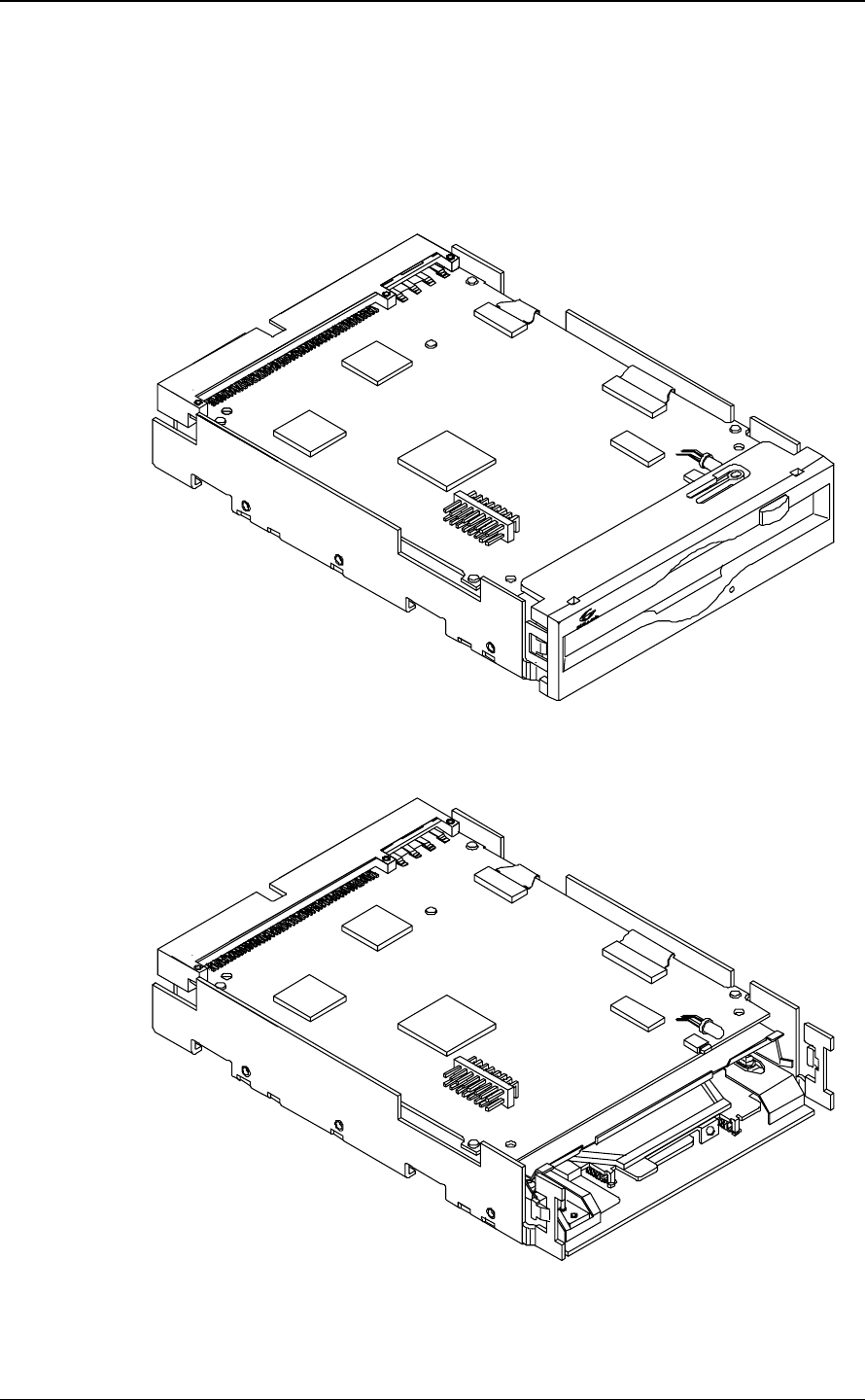
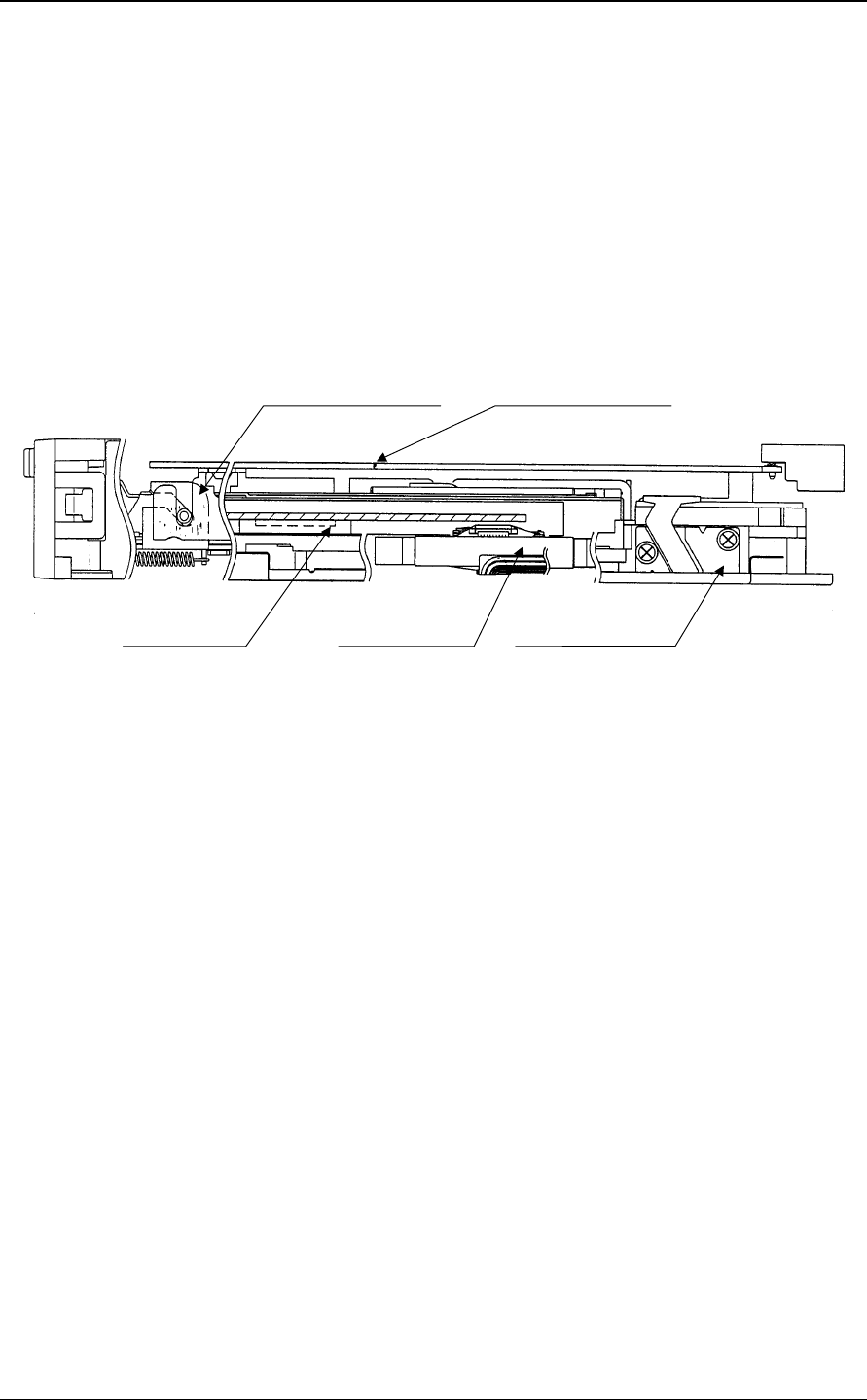
Figure 1.3 shows the drive configuration.
The drive consists of mechanical sections, a fixed optics section, actuator, and a
control circuit section. The mechanical sections include the spindle motor,
actuator section, bias magnet, and the cartridge folder vertical motion mechanism.
The fixed optics section consists of the optical components, position detector, and
LD controller.
The control circuit sections include the drive control circuit section and SCSI
controller section.
Figure 1.3 Optical disk drive configuration
Fixed optics sectionActuator section
Control circuit section
Spindle motor
Optical disk cartridge

1.2 Drive Configuration
C156-E224-01EN 1-9
1.2.3 Mechanical sections
(1) Optical disk cartridge load/eject
The system includes a cartridge mechanism which lowers the optical disk cartridge
and mounts (loads) it on the spindle motor automatically when the optical disk
cartridge is fully inserted in the optical disk drive's disk slot, and a mechanism
which automatically ejects the cartridge when the Eject button on the front panel is
pressed.
(2) Spindle motor
Optical disk cartridge hubs are linked through magnetic clamps to minimize
slippage between the spindle motor shaft and disk. The spindle motor is the direct
drive type which rotates the disk at the same speed as the spindle motor shaft. A
DC brushless spindle motor is used. The spindle motor rotates at 5,455 rpm ±
0.1%.
(3) Actuator section
The positioner moves (seeks) a head actuator radically across the disk surface.
The positioner is driven by a linear voice coil motor. A pulse-width modulation
(PWM) is adopted as a driving system and realizes low power consumption and
high-speed access.
(4) Separate optical sections
The optical head section is separated in such a way that the fixed optics section
is separated from the moving optics section to minimize seek time and positioning
error. (See Subsection 1.2.4 for the fixed optical section.) This reduces the weight
of the moving parts.
The fixed optics section consists of the laser diodes, collimator lens, and optical
detector.
The fixed optics section includes a laser diode for recording and playback, and
transmits one laser beam to the head actuator.
(5) Panel
The central part of the panel is hollowed out deeply to provide pushing finger
space for inserting the cartridge, thereby facilitating the insertion.
The panel is also simply designed by making the eject button and LED light
emitting part integral with each other.
General Description
1-10 C156-E224-01EN
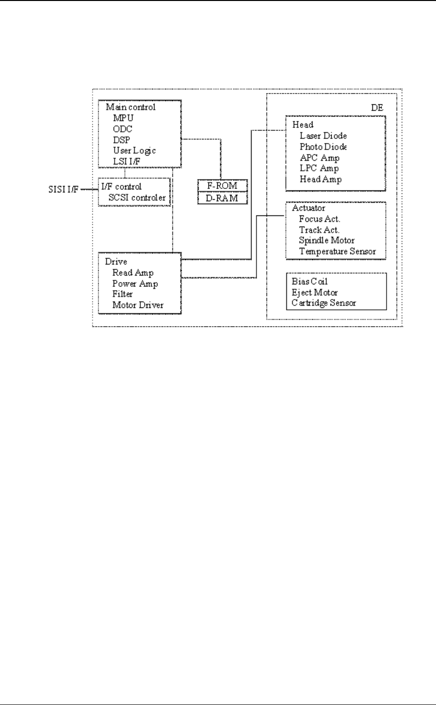
1.2.4 Control circuit section
Figure 1.4 is the block diagram of the control circuit section.
Figure 1.4 Control circuit section block diagram
The control circuit section is divided into two parts: a controller section which
deals with control between the SCSI interface and drive interface, and a drive
circuit section which controls the drive.
(1) Controller circuit section
The controller circuit's reliability is improved by large-scale integrated circuit
technology. The high-speed microprocessor (MPU) handles SCSI interface
control and drive control such as drive read-and-write control and single-beam
control.
(2) Drive circuit section
The drive circuit section consists of the following circuits:
• Laser diode control circuit
• Signal reproduction circuit
• Servo/seek control circuit
• Rotation control circuit
• Drive miscellaneous control circuit

1.2 Drive Configuration
C156-E224-01EN 1-11
The DSP (digital signal processor) is used for the servo/seek control circuit to
reduce the circuit amount, therefore this circuit is a simple configuration.
The drive circuit section executes operations such as seek, erase, record, and
playback while the MPU controls the focus-tracking of the beam.
This page is intentionally left blank.

C156-E224-01EN 2-1
CHAPTER 2 Specifications
This chapter contains the specifications of the optical disk drive, and the optical
disk cartridge.
2.1 Optical Disk Drive Specifications
2.1.1 Model and product number
Table 2.1 lists the model and order number.
Table 2.1 Model and order number
Model Name Order No. Panel Panel Color Mounting Screws
MCJ3230SS CA05890-B001 with panel Light gray
(2.5Y 7.2/0.4)
Metric screws (M3)
CA05890-B201 without panel Metric screws (M3)
CA05890-B101 with panel Light gray
(2.5Y 7.2/0.4)
Metric screws (M3)
Note: The panel colors (2.5Y 7.2/0.4) are indicated in Munsell symbols. (JIS
Z8721)
2.1 Optical Disk Drive Specifications
2.2 Optical Disk Cartridge Specifications
2.3 Defect Management

Specifications
2-2 C156-E224-01EN
2.1.2 Drive specifications
Table 2.2 lists MCJ3230SS drive specifications
Table 2.2 Specifications (1 of 2)
Item Specifications
Optical disk cartridge 128 MB media 230 MB media 540 MB media 640 MB media 1.3 GB media 2.3 GB media
Total capacity Unformatted 181 MB 325 MB 819 MB 818 MB 1.683 GB 2.901 GB
Formatted 128 MB 230 MB 538 MB 643 MB 1.283 GB 2.261 GB
Capacity/track Unformatted 18,100 bytes 18,100 bytes
(logical track
capacity)
19,450 bytes
(logical track
capacity)
43,928 bytes
(logical track
capacity)
45,798 bytes
(logical track
capacity)
47,022 bytes
(logical track
capacity)
Formatted 12,800 bytes 12,800 bytes
(logical track
capacity)
12,800 bytes
(logical track
capacity)
34,816 bytes
(logical track
capacity)
34,816 bytes
(logical track
capacity)
34,816 bytes
(logical track
capacity)
Capacity/sector Unformatted 725 bytes 778 bytes 778 bytes 2,584 bytes 2,694 bytes 2,766 bytes
Formatted 512 bytes 2,048 bytes
Number of user tracks/side *1 10,000 17,940 42,042 18,480 36,855 64,944
Number of alternate sectors/side ≤1,024 ≤1,025 ≤2,250 ≤2,244 ≤4,437 ≤8,976
Number of sectors/track 25 17
Data transfer rate 1.65 MB/s (max.)
0.39 MB/s
continuous
writing (effective)
1.16 MB/s
continuous
reading (effective)
2.00 to 3.16 MB/s
(max.)
0.47 to 0.75 MB/s
continuous
writing (effective)
1.40 to 2.23 MB/s
continuous
reading (effective)
3.45 to 5.94 MB/s
(max.)
0.78 to 1.30 MB/s
continuous
writing (effective)
2.33 to 3.91 MB/s
continuous
reading(effective)
3.52 to 5.87 MB/s
(max.)
0.93 to 1.55 MB/s
continuous
writing (effective)
2.79 to 4.66 MB/s
continuous
reading (effective)
3.92 to 6.70 MB/s
(max.)
0.99 to 1.70 MB/s
continuous
writing (effective)
2.98 to 5.09 MB/s
continuous
reading (effective)
5.17 to 6.70 MB/s
(ZCLV max.)
continuous
writing
(ZCLV effective)
1.31 to 1.70 MB/s
continuous
reading
(ZCLV effective)
3.93 to 5.09 MB/s
4.69 to 8.38 MB/s
(max.)
1.16 to 2.07 MB/s
continuous
writing (effective)
3.84 to 6.21 MB/s
continuous
reading (effective)
Random seek time *2 19 ms (typ)
Average latency 5.5 ms 8.2 ms
7.2 ms (ZCLV)
6.3 ms (ZCLV)
8.2 ms
Rotational speed 5.455 rpm 3,637 rpm
4,138 rpm
(ZCLV)
4,801 rpm(ZCLV)
3,637 rpm
Heads Positioner + Separete Optical Section
Positioner type Linear voice coil motor
Servo tracking method ISO continuous servo method

2.1 Optical Disk Drive Specifications
C156-E224-01EN 2-3
Table 2.2 Specifications (2 of 2)
Item Specifications
Optical disk cartridge 128 MB media 230 MB media 540 MB media 640 MB media 1.3 GB media 2.3 GB media
Density 24,424 bpi
(1.04µm/bit)
15,875 tpi
29,308 bpi
(0.87µm/bit)
18,275 tpi
52,900 bpi
(0.48µm/bit)
23,090 tpi
89,100 bpi
(0.285µm/bit)
28,200 tpi
112,474 bpi
(0.228µm/bit)
37,910 tpi
Loading time *3 8 sec. (typ) 12 sec. (typ) 14 sec. (typ)
Unloading time *4 4 sec. (typ)
Load/unload life 20,000
Host interface SCSI (SCSI-2 standard)
Data Transfer Model and rates Asynchronous transfer 5MB/s
Synchronous transfer 20MB/s
Data buffer 7,600 KB
Error correction *5 Correctable up to 8-byte/interleave
Bit error rate: 10-12 or less
*1 The number of user tracks indicates the maximum user zone which includes
the spare area and slipping area.
*2 Mathematical average of 1,000 times of seek and does not include command
overhead nor track address recognition time. Furthermore, it may depend
on the quality of media and drive installation environment.
*3 Loading time is the time from when the optical disk cartridge is inserted to
when the optical disk drive is ready.
*4 Unloading time is the time from when the eject button is pressed or the eject
command is issued to when the optical disk cartridge is ejected.
*5 Thebiterrorratemustbe10
-12 or less when a disk whose raw error rate is
10-4 or less is used.

Specifications
2-4 C156-E224-01EN
2.1.3 Environmental and power requirements
Table 2.3 lists the environmental and power requirements.
Table 2.3 Environmental and power requirements (1 of 2)
Item Specification
Power
requirements
Average +5 VDC±5%, 1.4 A (2.5 A Max.) *1
Ripple requirement 100mV P-P (DC-1 MHz)
Ready (active mode) 4.8 W (typical) *2
Random seek, read/ write 6.5 W (typical) *2
Physical Format 7.3 W (typical) *2
Power
consumption
(Average)
Power save mode
Pre-idle mode
Idle mode
Standby mode
4.0 W (typical) *2
2.0 W (typical) *2
1.0 W (typical) *2
With panel 101.6 ×150.0 ×25.4 mm
Dimensions
(W×D×H) Without panel 101.6 ×148.4 ×25.4 mm
Weight 480 g (with panel)
Environmental
requirements
Operating Temperature: 5 to 45°C *3
(gradient 15°C /h or less)
Relative humidity: 10 to 85% (Noncondensing)
Max. wet bulb temperature: 29°C or lower
Non Operating Temperature: 0 to 50°C
Relative humidity: 10 to 85% (Noncondensing)
Max. wet bulb temperature: 36°C or lower
Transport Temperature: -40 to 60°C (24 hours or less)
Temperature: -20 to 60°C (24 hours or more)
Relative humidity: 5 to 90% (Non condensing)
Max. wet bulb temperature: 41°C or lower
Installation Tilt angle -5° to +10° *3
Vibration/
shock
Operating 3.9 m/s2(5 to 500 Hz, sine sweep)
1.96 m/s2
(5 to 500 Hz, sine sweep AV record/play)
Shock 19.6 m/s2(10ms, half-sine pulse)
Non Operating
No cartridge, power ON
9.8 m/s2(5 to 500 Hz, sine sweep)
Shock 49 m/s2(10 ms, half-sine pulse)
Transport Shock 490 m/s2(10 ms, half-sine pulse)
Requirement: Packing conditions specified by
Fujitsu

2.1 Optical Disk Drive Specifications
C156-E224-01EN 2-5
Table 2.3 Environmental and power requirements (2 of 2)
Item Specification
Altitude Operating 3,000 m (10,000 ft) or less
Non Operating 12,000 m (40,000 ft) or less
Air flow Unused *4Ambient for
purity Air purity General office environment or better
(dust perticles: Class 5 millions or less)
Note:
*1 At random seek or read/write. Excluding pulse waveform under 500 us or
less.
*2 It demonstrates in an installation environment of a temperature of 25°C,
voltage of 5 V.
See Section 4.4.8 for information on the power management function.
*3 The efficiency is specified in an environment of a temperature of 25°C and
0° horizontal level placement.
*4 For details, refer to section 3.1.3 'Air Flow'
1. Current limiter value for +5 VDC power: 5 A or less
2. Specifications under transporting condition are under the packaging specified
by Fujitsu.
3. A voltage drop may occur depending on the used power supply or power
cable.
4. If power for the terminators in the other SCSI devices is supplied via an
optical disk drive, note that the current of the +5VDC power for the optical
disk drive may increase by a maximum of 200 mA. The method of supplying
power to terminators cannot be changed.
5. Table 2.4 lists power consumption in power save mode when the temperature
inside the drive is 20°C or lower.
Table 2.4 Power consumption in power save mode when the temperature inside the
drive is 20°C or lower
IETM Power consumption at 20°C or lower
Pre-idle mode 4.0W (typ)
Idle mode 2.0W (typ)
Power consumption in
power save mode
Standby mode 1.0W(typ)
6. If the temperature inside the drive is 14°C or lower, disk access might become
longer because the speed of the related mechanisms varies with temperature.

Specifications
2-6 C156-E224-01EN
2.1.4 Error rate
Data blocks to be accessed are evenly distributed on the disk. Errors due to disk
defects are not included.
(1) Bit error rate after ECC processing
The error rate after ECC processing must be 10-12 or less. An optical disk cartridge
whose raw error rate is 10-4 or less should be used.
(2) Positioning error rate
The positioning error rate must be 10-6 or less. (with retry)
2.1.5 Reliability
(1) Mean time between failures (MTBF)
The MTBF is 120,000 hours or more. Failure due to disk errors is not included.
Conditions
• Power-on time: 200 hours/month or less
• LD-on time: 20% or less of power-on time
• Environment Temp.: 25°C
Note:
The MTBF is defined as follows:
- Operating time is the total time power is applied.
- Device failures indicate that devices require repair, readjustment, or
replacement. Failure due to external factors such as minor defects
during device handling, operation outside environmental
specifications, power failure, host system errors, and interface cable
errors are not included.
(2) Service Life
Under appropriate handling and operation, disk cleaning and optical head
cleaning, overhaul of the drive is not required for the first five years.
(3) Data security at power failure
Except for the data of the block to which write operation is in progress, all data on
the disk is secure from power failure. This does not apply if power failure occurs
during disk initialization (formatting) or defect processing (alternate block
allocation).
total operating time in all fields (hours)
MTBF=
number of device failure in all fields

2.2 Optical Disk Cartridge Specifications
C156-E224-01EN 2-7
2.2 Optical Disk Cartridge Specifications
2.2.1 Recommended optical disk cartridge specifications
The following three disk types comply with the specifications.
Table 2.5 shows the specifications of the optical disk cartridge recommended for
this optical disk drive. The use of another disk cartridge may lower drive
performance.
Table 2.5 Recommended optical disk cartridge specifications
Model Order number Figure number
Optical disk cartridge (128 MB) 0242110 CA90002-C010
Optical disk cartridge (230 MB) 0242210 CA90002-C011
Optical disk cartridge (540 MB) 0242410 CA90002-C012
Optical disk cartridge (640 MB) 0242610 CA90002-C013
Optical disk cartridge (1.3 GB) 0242810 CA90002-C015
Optical disk cartridge (2.3 GB) 0242910 CA90002-C030
Overwrite optical disk cartridge (230 MB) 0242310 CA90002-C041
Overwrite optical disk cartridge (540 MB) 0242510 CA90002-C042
Overwrite optical disk cartridge (640 MB) 0242710 CA90002-C043
Specifications
2-8 C156-E224-01EN
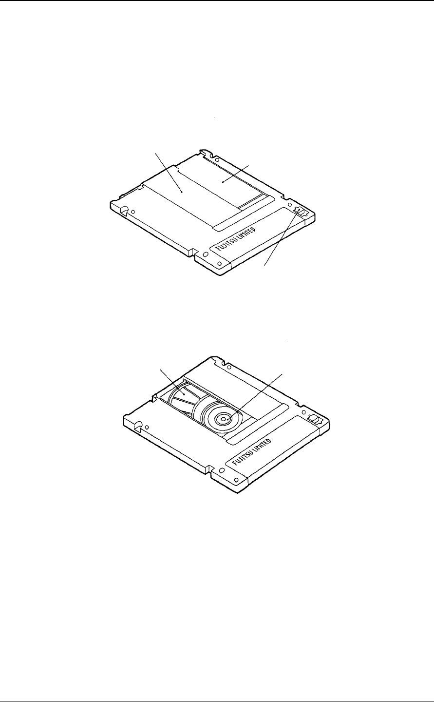
2.2.2 Optical disk cartridge
Figure 2.1 shows an optical disk cartridge. The figure below shows the cartridge
with its shutter open.
a. Shutter closed
b. Shutter open
Figure 2.1 Optical disk cartridge
3) Write protect tab
1) Cartridge case
2) Shutter
4) Disk 5) Hub

2.2 Optical Disk Cartridge Specifications
C156-E224-01EN 2-9
The following explains the components of the optical disk drive shown in Figure
2.1:
1) Cartridge case
Covers the disk to protect it from damage when handled and facilitates disk
replacement. The cartridge case is labeled and has a write protect tab.
2) Shutter
Protects the disk against dust. When the cartridge is inserted into the optical
disk drive, the shutter (metallic door) is opened.
3) Write protect tab
The write protect tab selects whether write is enabled or disabled.
4) Disk
Holds information which can be read by an optical beam.
5) Hub
The hub is placed at the center of the disk and is linked to the spindle of the
drive. The hub is used for radial centering and axial positioning.
2.2.3 Disk specifications
(1) 128 MB disk
The ISO/IEC10090 defines 128 MB disk specification.
(2) 230 MB disk
The ISO/IEC13963 defines 230 MB disk specification.
(3) 540 MB/640 MB disk
The ISO/IEC15041 defines 540 MB/640 MB disk specification.
(4) 1.3 GB disk
The Cherry Book defines 1.3 GB disk specification.
(5) 2.3 GB disk
The Cherry Book 2 defines 2.3 GB disk specification.
Table 2.6 lists disk specifications.

Specifications
2-10 C156-E224-01EN
Table 2.6 Disk specifications
Item Specification
Reliability Read cycle >108
Erase/write/read cycle >106
Load/unload cycle 25,000
Archival life (according to acceleration test results) >10 years *1
Shelf life (according to acceleration test results) >10 years *2
Operating temperature 5 to 55°CEnvironmental
requirements Operating relative humidity 3 to 85%RH *3
Storage temperature -20 to 55°C
Storage humidity 3 to 90% RH *3
*1 Archival life is the period in which recorded information can be read.
*2 Shelf life is the period in which information to be recorded can be written.
*3 Maximum wet bulb temperature = 29°C.
Note:
Non-recommended disks must be checked for compatibility.
2.3 Defect Management
C156-E224-01EN 2-11
2.3 Defect Management
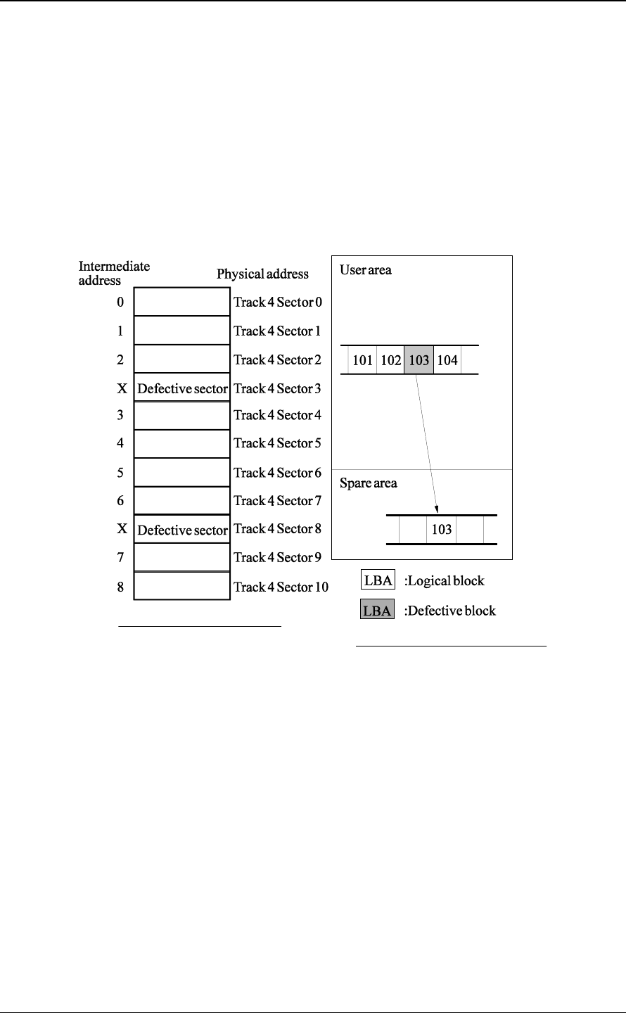
2.3.1 Defect management schematic diagram
Defective sectors on the disk shall be replaced by good sectors according to the
defect management scheme as follows: Defective sectors found during surface
certification are handled by a sector slipping algorithm. Defective sectors found
after initialization are handled by a linear replacement algorithm.
Figure 2.2 shows the algorithms for alternate processing.
(a) Sector slipping algorithm
(b) Linear replacement algorithm
Figure 2.2 Algorithms for alternate processing
The user area is divided into several groups during media initialization. Each
group contains data sectors and spare sectors. Spare sectors are used as
replacements for defective data sectors. Media initialization can include a
certification of the user area.
Figure 2.3 shows an example of alternate processing.
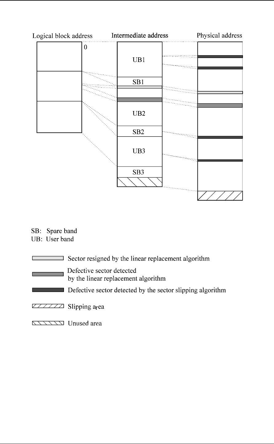
Specifications
2-12 C156-E224-01EN
Figure 2.3 Example of alternate processing

C156-E224-01EN 3-1
CHAPTER 3 Installation Requirements
This chapter describes environmental, mounting, power supply, and connection
requirements.
3.1 Environmental Requirements
The environment in which these drives are installed must comply with the ambient
environmental requirements defined in Subsection 2.1.3.
3.1.1 Temperature measurement point
When a drive is operating, the ambient temperature measured 3 cm from the base
surface of the optical disk drive and the PCA unit surface must satisfy the
environmental requirements specified in Subsection 2.1.3. For the temperature of
each surface during operation, the contact temperature at each measurement point
shown in Figure 3.1 must satisfy the requirements specified in Subsection 3.1.2.
Low temperature burns: The surface temperatures of some ICs
on the printed circuit board unit in the optical disk drive exceed
55°C while operating. Be careful of low tenperature burns.
3.1 Environmental Requirements
3.2 Mounting Requirements
3.3 Power supply Requirements
3.4 Cable Connections
3.5 Settings
3.6 Notes on Drive Handling
3.7 Mounting
3.8 Cable Connections
3.9 Operation Confirmation and Preparation for Use after Installation
3.10 Dismounting Drive
Installation Requirements
3-2 C156-E224-01EN
a) Inside optical disk cartridge
b) IC (controller, read amp)
IC (controller) IC (read amp)
IC (power amp)
Figure 3.1 Surface temperature measurement points
Hole for inserting thermocouple Tip of thermocouple
Operating of inner
partition wall

3.1 Environmental Requirements
C156-E224-01EN 3-3
3.1.2 Temperature requirements and measuring method
Table 3.1 shows the temperature requirement at each measurement point shown in
Figure 3.1.
Table 3.1 Temperature requirements at measurement points
Measurement point Maximum surface temperature
Cartridge inside 55°C *
IC (controller) surface 90 °C
IC (read amp.) surface 95 °C
IC (power amp.) surface 90 °C
* Following procedure is for temperature measurement of inside cartridge.
1) Make a hole for the thermocouple as shown in Figure 3.1.
2) Disassemble the cartridge disk.
3) Cut off a part of the partition wall for the optical media as shown in Figure
3.1. (Cut off width: 5 to 10 mm)
4) Fix the tip of the thermocouple to the cut portion of partition wall with an
adhesive agent.
5) Pass the thermocouple through the hole at the cartridge case and assemble the
cartridge disk. When there is a gap between the hole and the thermocouple,
fill the gap with the adhesive agent.
Note:
The surface of the cartridge shown in Figure 3.1 has been cut away to make
the elements inside the case clearly visible. In reality the surface is not cut
away.
If the external environment temperature is higher than the specified value, the
device will automatically take an interval to respond to command, and then
take protective action to respond to the temperature increase.
3.1.3 Air flow
It is recommended that this optical disk drive be installed in a fanless cabinet.
However, if the power supply is incorporated into the same cabinet, it is necessary
that it satisfy the "Temperature Conditions" in 3.1.2 and that the air flow rate
being drawn in by the device) at the cartridge loading slot be 0.3 m/s or lower.
Furthermore, if there is a system fan in a system where this drive is being installed,
the same conditions must be met.

Installation Requirements
3-4 C156-E224-01EN
3.1.4 Temperature rise under several conditions
Table 3.2 Temperature at each measuring point (Reference)
[Ambient atmospheric temperature of the optical disk drive: 45°C] (°C)
Measurement point Ready Random seek Criteria
Inside cartridge 47°C 54°C 55°C
IC (controller) surface 51°C 68°C 90°C
IC (read amp.) surface 48°C 90°C 95°C
IC (power amp.) surface 47°C 78°C 90°C
Thermal sensor 47°C 55°C −
Notes:
1. The above data are data estimated as they were measured where the
temperature surrounding the equipment was kept at 45 °C, using that at
25 °C. They are not the same as the data obtained from measurements
using the exclusive box in which the equipment is normally used.
2. When using the box, the ambient temperature around the equipment will
differ depending on the air circulation conditions of the box, and the
temperature rise inside the cartridge will differ because of this, so please
exercise caution.
3.1.5 Air purity
Air purity in the device environment is expressed by the number of dust particles
per unit area and must be class 5 millions (equivalent to 0.15 mg/m3)orless.
(Class 5 millions: 5 millions dust particles of 0.5 um dia. or larger per cubic foot)
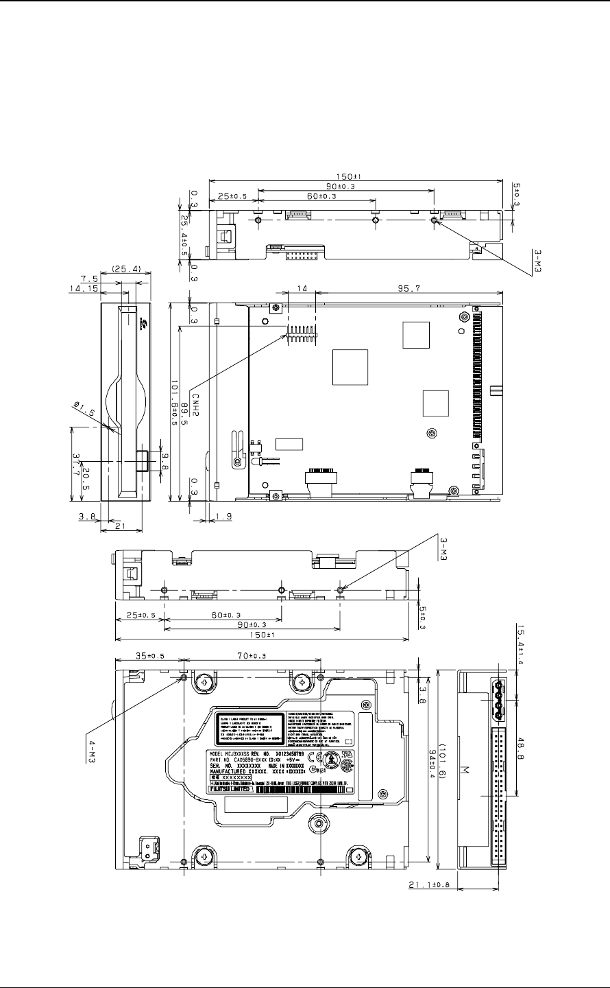
3.2 Mounting Requirements
C156-E224-01EN 3-5
3.2 Mounting Requirements
3.2.1 External dimensions
Figures 3.2 to 3.3 show the dimensions of the drive and the positions of the
mounting holes.
Unit: mm
Figure 3.2 Dimensions
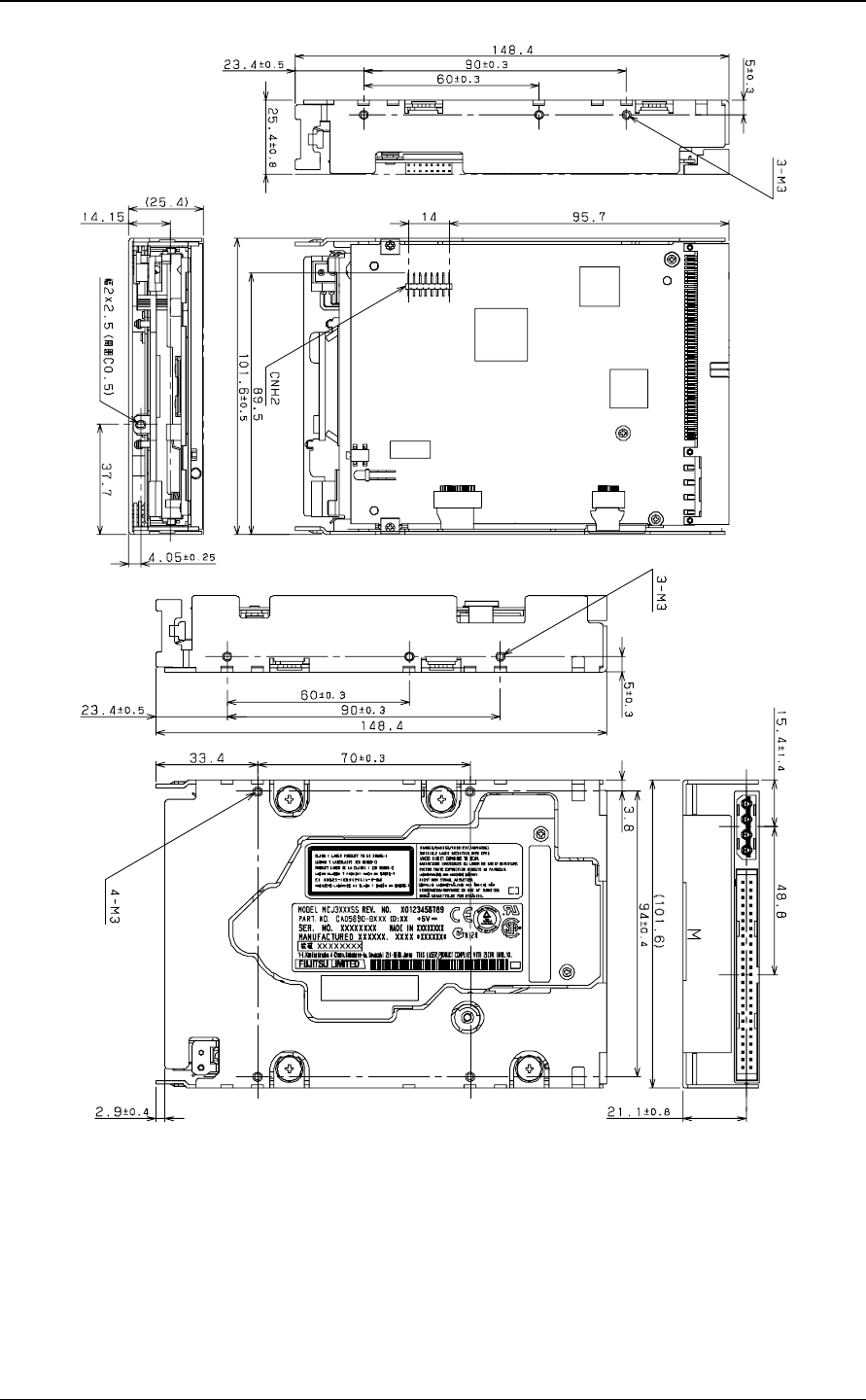
Installation Requirements
3-6 C156-E224-01EN
Unit: mm
Figure 3.3 Dimensions (without panel)
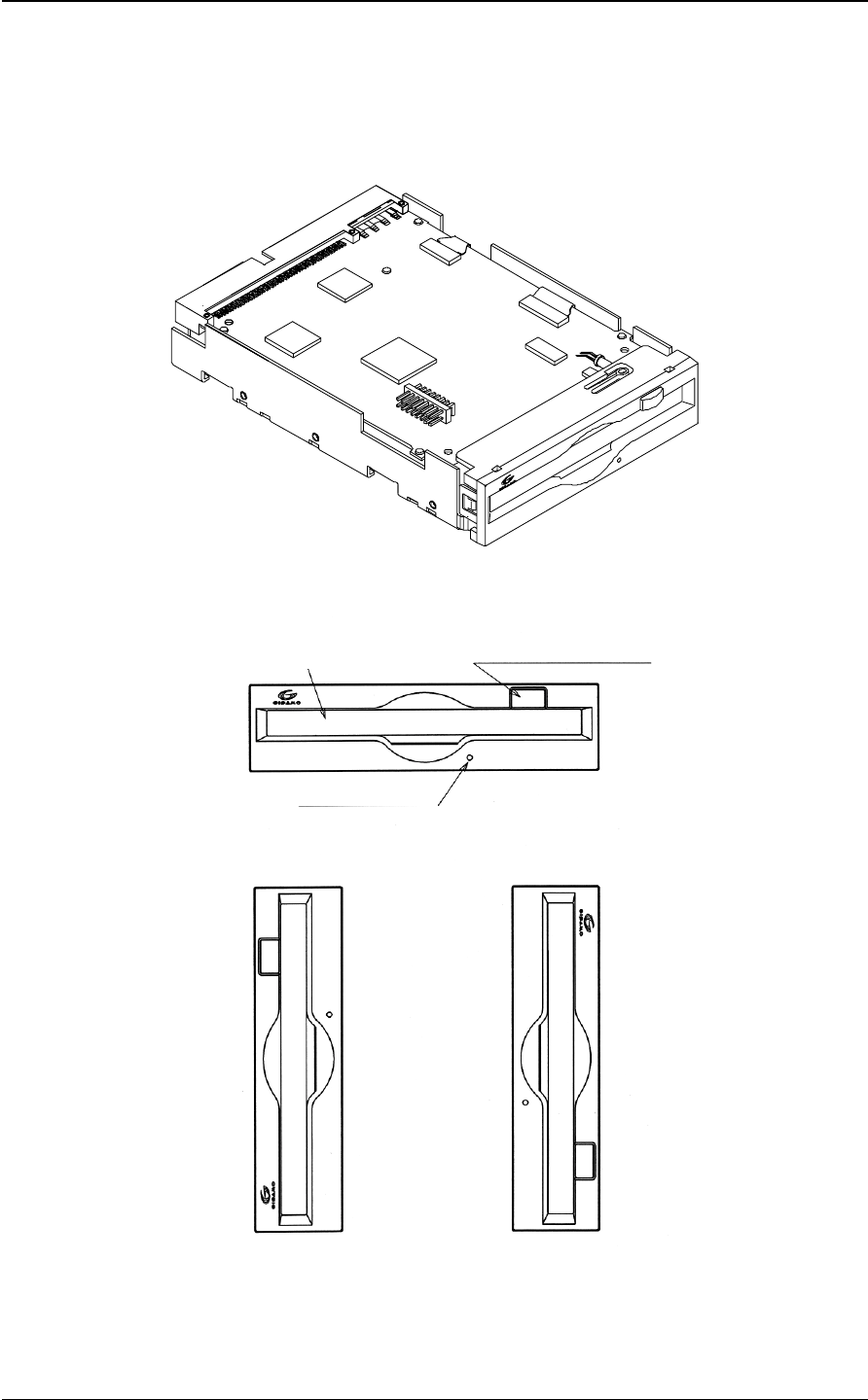
3.2 Mounting Requirements
C156-E224-01EN 3-7
3.2.2 Installation direction
Figure 3.4 shows the permissible installation directions for this drive. The
mounting angle tolerance must be within -5 to 10 from the horizontal. (-) shows
that the insertion faces below.
Eject button / Busy LED
Disk insertion slot
Manual eject hole
Figure 3.4 Installation directions
• Horizontal
• Vertical
(Two orientations)
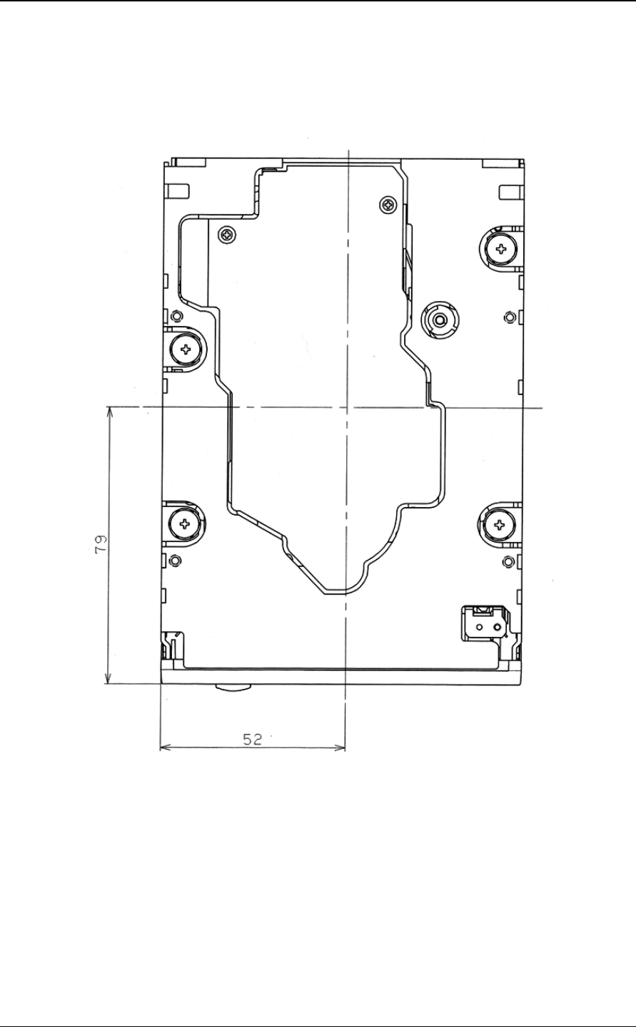
Installation Requirements
3-8 C156-E224-01EN
3.2.3 Centers of gravity
Figure 3.5 shows the centers of gravity of the drive.
Figure 3.5 Centers of gravity
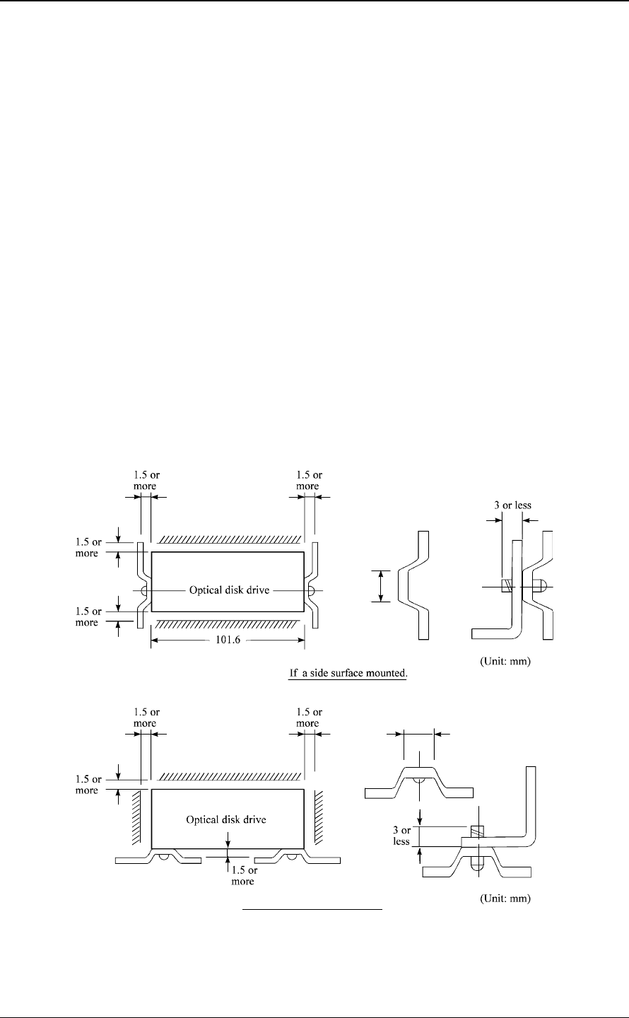
3.2 Mounting Requirements
C156-E224-01EN 3-9
3.2.4 Notes on mounting
(1) Mounting frame structure and clearance
a) For vibration resistance and heat dissipation, this optical disk drive uses an
embossed structure as shown in Figure 3.6, as well as a frame which has a
construction similar to other frames which perform the same function.
b) As shown in Figure 3.6, the inward projection of the mounting screw from the
outer surface of the drive frame must not exceed 3 mm.
c) The clearance between the external surface of the drive frame and the user's
frame structure must be at least 1.5 mm.
d) The clearance between the top and bottom surfaces and the user's frame
structure must be at least 1.5 mm.
e) When mounting the optical disk drive, the screw tightening torque should be
0.4 to 0.45Nm (4 to 4.6kgcm).
f) When the optical disk drive (with panel) is mounted in a locker, there should
be no deformation of the mounting fittings provided and the optical disk
drive's panel should not be deformed. If the drive is used with the panel
deformed, ejection of the cartridge will be faulty. Check if the door will close
from any position whatever when the optical disk drive is installed.
φ15
or less
φ15
or less
If a bottom surface mounted.
Figure 3.6 Mounting frame structure
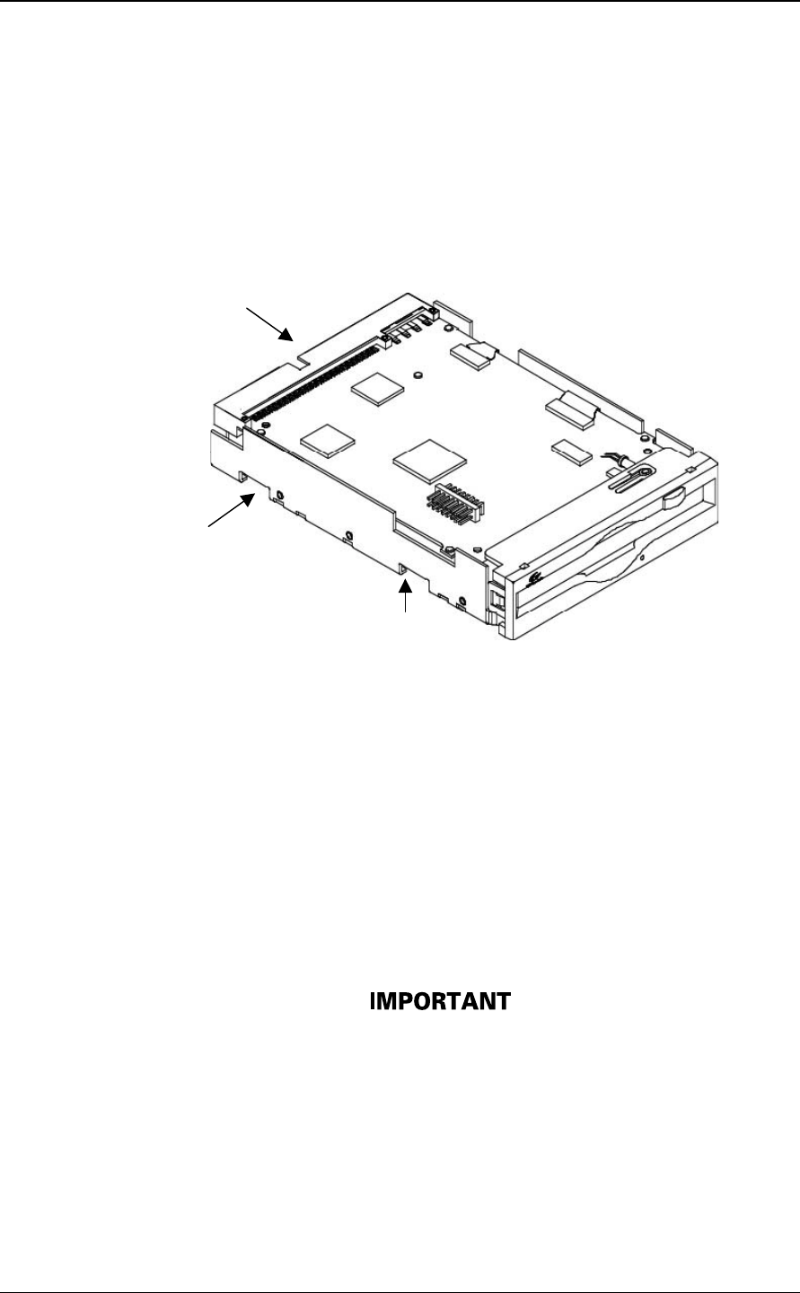
Installation Requirements
3-10 C156-E224-01EN
(2) Panel function processing
When installed in a cabinet, do not change the panel formal. The processing is
installation status and the disk insertion door can be closed from any locations.
(3) Service clearance
Figure 3.7 shows locations which must be accessed for installation and
maintenance. Be sure to leave sufficient service clearance.
P side
• Cable connection
R side
• Mounting screw hole
Q side
• Mounting screw hole
Figure 3.7 Service clearance
(4) External magnetic fields
Mount the optical disk drive away from powerful magnetic materials (e.g., a
speaker) to avoid influence from magnetic fields.
(5) Leak magnetic field
The VCM drive magnetic circuit may leak the magnetic field (Maximum 25 mT at
distance of 4 mm from the drive).
Do not place a device sensitive to a magnetic field near the optical
disk drive.
(6) External light source
Mount the optical disk drive away from strong light sources (e.g., camera flash).
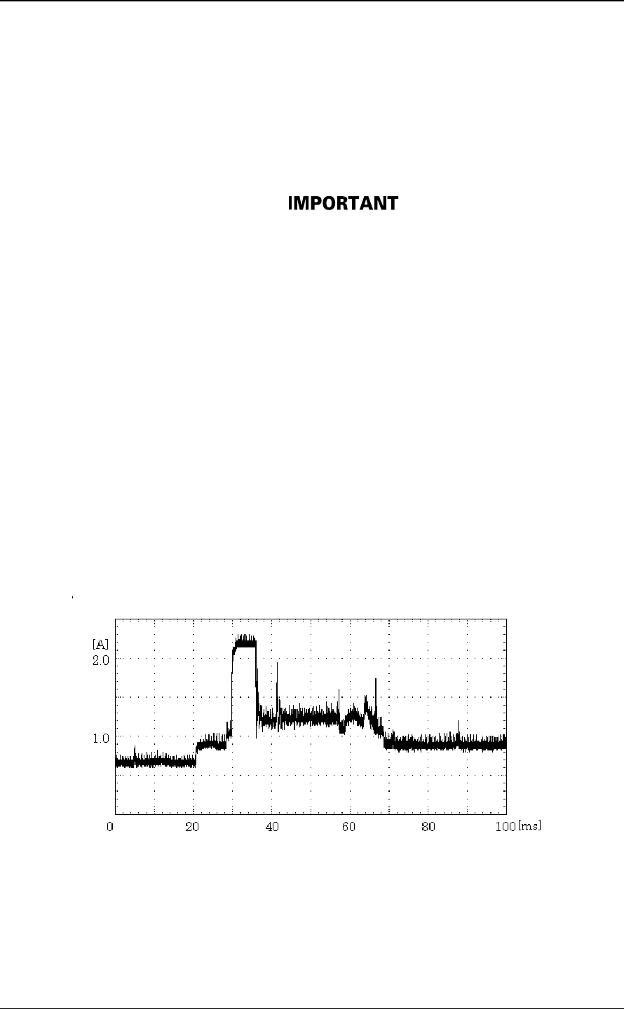
3.3 Power Supply Requirements
C156-E224-01EN 3-11
(7) System ground
The optical disk drive should be grounded to the signal ground (SG) of the power
supply of the system. This SG line should be supplied with the system.
The Frame Ground is shorted in the optical disk drive by a metal strip attached to
the vibration isolation rubber between the frame (FG) and the base (SG).
When mounting the optical disk drive in the Device Bay 120mm (5
inch) of the PC chassis, there are two ways of choosing frames the
metal frame and the plastic (nonconductive material) frame.
When using a plastic frame, there is not a short circuit between FG
of PC and FG of the optical disk drive. As a result, the static
electricity tolerance decreases compared with metal frame.
It is recommended to use a metal frame to enhance the static
electricity prevention.
3.3 Power Supply Requirements
(1) Allowable input voltage and current
The DC power supply input voltage measured at the power supply connector pin
of the optical disk drive (receiving end) must satisfy the requirements in Section
2.1.3.
(2) Current waveform (reference)
Figure 3.8 shows the +5 VDC waveform at seek.
Figure 3.8 Current waveform (+5 VDC)
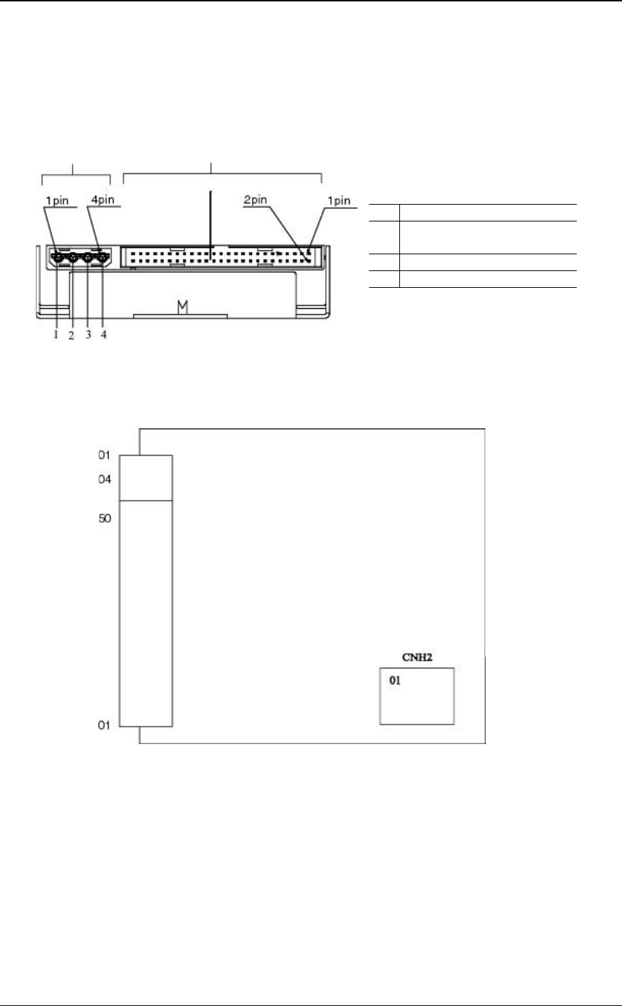
Installation Requirements
3-12 C156-E224-01EN
3.4 Cable Connections
3.4.1 Drive connectors
Figure 3.9 shows the connector and terminal locations.
1 + 12VDC or not connected
2 +12VDC RETURN (GND)
or not connected
3 + 5VDC RETURN (GND)
4 + 5VDC
Figure 3.9 Connector and terminal locations
Front
(Component side)
SCSI
connector
Power
connector
Figure 3.10 Location of setting terminal

3.4 Cable Connections
C156-E224-01EN 3-13
PC board
Figure 3.11 Shape of setting terminal

Installation Requirements
3-14 C156-E224-01EN
Table 3.3 Pin assignments
Pin No. Pin name Function
1 SCSI-ID (-) -
2 SCSI-ID1 SCSI ID1 setting *1
3 SCSI-ID (-) -
4 SCSI-ID2 SCSI ID2 setting *1
5 SCSI-ID (-) -
6 SCSI-ID4 SCSI ID4 setting *1
7 GND 0V
8 TERM SCSI Terminating resistor mode *2
9 GND 0V
10 Write Cache Mode Write cache mode *2
11 GND 0V
12 Spindle Automatic
Stop Mode
Automatic spindle stop mode *2
13 CTGIN Cartridge insertion signal *2 *3
14 EJSW Cartridge ejection signal *2 *4
15 LED (+)
16 LED (-) Operating status LED signal *5
*1 When pins 2, 4, and 6 are used, connect each pin to SCSI-ID (-).
*2 When pins 8, 10, 12, 13, and 14 are used, connect each pin to GND.
*3 This signal indicates that a cartridge is inserted in the device. This is a TTL
level signal.
H: A cartridge is present.
L: No cartridge is present.
*4 This signal is used to instruct cartridge ejection from outside.
*5 The LED uses a forward current of 20 mA or less.
If voltage is applied to pin 14 from outside, the device may be
damaged. When using this pin, be sure to connect it to GND.

3.4 Cable Connections
C156-E224-01EN 3-15
3.4.2 Cable connector specifications
Table 3.4 Recommended components for connection
Category Name Model Manufacturer
Cable socket
(closed-end type)
FCN-707B050-AU/B Fujitsu Ltd.
Cable socket
(through-end type)
FCN-707B050-AU/O Fujitsu Ltd.
UL20184-
LT25PX28AWG
Hitachi Cable,
Ltd.
SCSI cable
Signal cable
455-248-50 SPECTRA-
STRIP
Housing for cable
socket
1-480424-0 AMP
Contact 170121-4 AMP
Power supply
cable
Cable AWG18 -
Housing for cable
socket
LPC-16F02 Honda-Tsushin
Receptacle LPC-F104N Honda-Tsushin
Setting
terminal
Cable AWG28 -
A terminating resistor is mounted on the drive when the drive is
shipped. A terminating resistor must be disconnected when the
drive is not connected to an end of the SCSI cable.
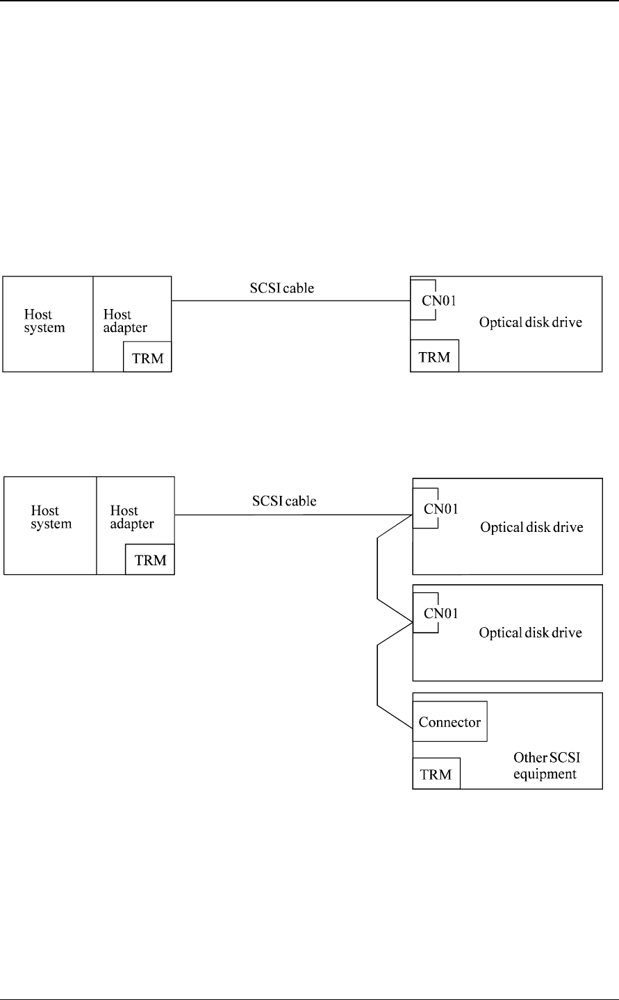
Installation Requirements
3-16 C156-E224-01EN
3.4.3 Connection Modes
Figure 4.3 shows examples of connections between the host system and the optical
disk drive. Up to eight devices including the host adapter, optical disk drive, and
other SCSI equipment can be connected to the SCSI bus in arbitrary combinations.
Install a terminating resistor on the SCSI devices connected to either end of the
SCSI cable.
See Section 3.4 for the cable connection requirements and power cable
connections.
a. Connecting one optical disk drive
b. Connecting more than one optical disk drive (single host)
Figure 3.12 SCSI bus connection modes
3.4 Cable Connections
C156-E224-01EN 3-17
c. Connecting more than one optical disk drive (multi-host)
Figure 3.13 SCSI bus connection modes
Note: If more than one SCSI device is connected to the same SCSI bus, Fujitsu recommends using
an external terminator.
Installation Requirements
3-18 C156-E224-01EN
3.5 Settings
3.5.1 Default jumper settings
Figure 3.14 shows the types of switches and their settings when the drive was
shipped.
Figure 3.14 Setting terminal (CNH2)
3.5.2 Setting terminal
(1) SCSI ID
Table 3.5 shows the SCSI ID settings of the drive.
Table 3.5 SCSI ID setting (CNH2)
SCSI ID Pin 5-6 Pin 3-4 Pin 1-2
0 Open Open Open
1 Open Open Short
2 Open Short Open
3 Open Short Short
4 Short Open Open
5 Short Open Short
6 *1 Short Short Open
7 Short Short Short
*1 Factory setting

3.5 Settings
C156-E224-01EN 3-19
1) Each SCSI device connected to the same SCSI bus must have a
unique SCSI ID.
2) If contention occurs in the ARBITRATION phase, the priority
of the SCSI use authority depends on SCSI IDs as follows:
7>6>5>4>3>2>1>0
(2) SCSI terminating resistor mode
Enabling or disabling the SCSI terminating resistor, module on the PCA can be
set.
When the drive positions at other than the end of the SCSI bus, the SCSI
terminating resistor should be disabled. Table 3.6 shows the SCSI terminating
resistor mode setting.
Table 3.6 SCSI terminating resistor mode
SCSI terminating resistor mode (7-8)
SCSI terminating resistor module on the PCA is enabled. SHORT *1
SCSI terminating resistor module on the PCA is disabled. OPEN
*1 Factory setting
(3) Write cache mode
The write cache mode can be set. The write cache mode can also be enabled or
disabled by the MODE SELECT command.
Table 3.7 shows the settings of the write cache mode.
Table 3.7 Write cache mode setting
Write cache mode (9-10)
Write cache is disabled at executing the WRITE/WRITE
AND VERIFY command
OPEN
Write cache is enabled at executing the WRITE/WRITE
AND VERIFY command.
SHORT *1
*1 Factory setting

Installation Requirements
3-20 C156-E224-01EN
When the write cache feature is enabled, a write error is reported at
the completion status of next command. At a system so that the
initiator retries the command, a retry process may be failed.
(4) Spindle automatic stop mode
The optical disk drive automatically enters standby mode if it receives no
commands from the host for about 32 minutes (default value).
Table 3.8 Spindle motor automatic stop mode setting
Spindle motor automatic stop mode (11-12)
The spindle motor automatically stops after a
specified period of time.
SHORT
The spindle motor does not stop. OPEN *1
*1 Factory setting

3.6 Notes on Drive Handling
C156-E224-01EN 3-21
3.6 Notes on Drive Handling
(1) General notes
Note the following points to maintain drive performance and reliability:
Device damage:
1) Shock or vibration applied to the drive that exceeds the values
defined in the standard damage the drive. Use care when
unpacking.
2) Do not leave the drive in dirty or contaminated environments.
3) Since static discharge may destroy the CMOS devices in the
drive, pay attention to the following points after unpacking:
- Use an antistatic mat and wrist strap when handling the
drive.
- Hold the mounting frame when handling the drive. Do
not touch the Printed circuit board except when setting the
switches.
4) When handling the drive, hold both sides of the mounting
frame. When touching other than both sides of the mounting
frame, avoid putting force.
5) Do not forcibly push up the end of the header pin of the printed
circuit board unit when handling or setting the drive.
(2) Unpacking
•Make sure that the UP label on the package is pointing upward and start
unpacking on a level surface. Handle the drive on a soft surface such as a
rubber mat, not on a hard surface such as a desk.
•Use care to avoid exerting excessive pressure on the unit when removing the
cushions.
•Use care to avoid exerting excessive pressure on the printed circuit board
surface and interface connectors when removing the drive from the antistatic
bag.
•If the temperature difference between installation locations is 10 degrees or
more, leave the drive in the new location for at least two hours before
unpackaging it.

Installation Requirements
3-22 C156-E224-01EN
(3) Installation
•Do not connect or disconnect the connectors or change the terminal settings
when the power is on.
•Do not move the drive with the power on.
•Eject the optical disk cartridge, lock the carriage securing the head, turn off
the power, then move the drive.
Device damage: Be sure to turn on the power supply before
inserting your cartridge for the first time. It releases the device from
transport protection and enables you to insert the cartridge.
The device may be damaged if you insert the cartridge without
releasing the protection. From the next time, you don't need to turn
on the power supply beforehand.
Before moving the drive, remove the optical disk cartridge. If the
drive is moved with the optical disk cartridge loaded in it, the head
may move back and forth in the drive to damage the head or disk
and reading the data may fail.
(4) Packing
•Before packing, remove the optical cartridge.
•Store the drive in an antistatic plastic bag with desiccant (silica gel).
•Use the same cushions and packaging supplied with the drive. If they are not
available, ensure that adequate shock absorbent material is used. In this case,
some method of protecting the printed circuit board surface and interface
connectors must be used.
•Apply "UP" and "Handle With Care" labels to the outside of the package.
Figure 3.15 shows the single-unit packing style and the multiple-unit packing
style. (The form and material of the cushion may be changed.)
3.6 Notes on Drive Handling
C156-E224-01EN 3-23
Eject pin (use a sealing tape)
Support (Front, Rear)
Eject pin (x 20)
Support (Middle)
Box
Shipping Label (2)
Master carton
(
12/24 units
)
Single-unit packing Multiple-unit packing
Conductive bag
MCJ3230SS
MCJ3230SS
Desiccant Desiccant
Figure 3.15 Packing style
(5) Transportation
•Transport the optical disk drive packed in principle, with the UP sign upward.
•After unpacking, minimize the transportation distance and use cushions to
avoid shock and vibration. Transport the drive in one of the orientations
described in Subsection 3.2.2 after unpacking. (The horizontal direction is
recommended.)
(6) Storage
•Use moistureproof packaging when storing the drive.
•The storage environment must satisfy the requirements specified in
Subsection 2.1.3 when the drive is not operating.
•To prevent condensation, avoid sharp changes in temperature.
Conductive bag

Installation Requirements
3-24 C156-E224-01EN
3.7 Mounting
3.7.1 Checks before mounting the drive
Before mounting the optical disk drive in the system cabinet, check whether the
jumper settings are set correctly.
3.7.2 Mounting procedure
How the drive is mounted depends on the system cabinet structure. Determine the
mounting procedure in consideration of the requirements of each system. This
section contains the general mounting procedure and check items.
See Section 3.2 for details on mounting drive.
1) Tighten four mounting screws to secure the drive in the system cabinet.
− The drive has ten mounting holes (both sides: 3 ×2, bottom: 4). Secure
the drive using the four mounting holes on both sides or the bottom.
− Use mounting screws whose lengths are 3 mm or less from the external
wall of the mounting frame of the drive when they are tightened. (See
Figure 3.6)
− When mounting with screws, the screw tightening torque should be 0.4 to
0.45Nm (4 to 4.6kgfcm).
− Be careful not to damage the parts on the PCA when mounting the drive.
2) After securing the drive, make sure that the drive does not touch the chassis of
the system cabinet. There must be at least 1.5 mm clearance between the
drive and chassis. (See Figure 3.6)

3.8 Cable Connections
C156-E224-01EN 3-25
3.8 Cable Connections
Use the following cables to connect the drive to the system. See Subsection 3.4
for details on the connector positions and cable requirements.
• Power supply cable
• SCSI interface cable
• DC ground cable (if required)
The general procedure for cable connection and notes on connecting cables are
given below. Pay attention to the insertion direction of each cable connector.
•Make sure that the system power is off.
•Do not connect or disconnect any cable when the power is on.
1) Connect the DC ground cable (only if required to decrease ground noise).
2) Connect the power cables.
3) Connect the SCSI interface cable.
4) After each cable connector is connected, secure the cable so that the cable
does not touch the drive or the parts on the PCA or obstruct the flow of
cooling air in the system cabinet.

Installation Requirements
3-26 C156-E224-01EN
3.9 Operation Confirmation and Preparation for Use after
Installation
3.9.1 Confirming initial operations
This section provides the operation check procedures after the power is turned on.
(1) Initial operation when the power is turned on
• When the power is turned on, the drive starts initial self-diagnosis. The LED
on the front panel is on for 1 second during initial self-diagnosis.
• If an error is detected during initial self-diagnosis, the LED on the front panel
blinks.
• In case of not inserted the cartridge, when the power is turned on, the eject
motor automatically turns once.
(2) Checks if errors occur at initial self-diagnosis
• Make sure that the cables are connected correctly.
• Make sure that the supply voltage is correct. (Measure the voltage at the
power supply connector of the optical drive.)
• Make sure that the settings of all terminals are correct.
• If the LED on the front panel blinks continuously, an error was detected
during initial self-diagnosis. In this case, issue the REQUEST SENSE
command from the initiator (host system) to obtain sense data for error
analysis.
The BUSY LED is on while the optical disk drive is executing seek,
write, or read operations. The BUSY LED is on momentarily, so it
seemsasifitblinkedorisoff.
The eject motor turns once when the power is turned on so that in
case the spindle motor position deviates due to shocks received by
the drive during transport the position is corrected to allow the
cartridge to be inserted normally. If the cartridge fails to be inserted,
remove the cartridge and turn on the drive power to turn the eject
motor once and reinsert the cartridge.

3.10 Dismounting Drive
C156-E224-01EN 3-27
3.9.2 Connection check
When initial operation check terminates normally after the power is turned on,
check whether the drive is correctly connected by issuing command from the host
system. Checking procedure depends on the host system configuration.
If processing terminates abnormally:
1) If sense data has been obtained by the REQUEST SENSE command, analyze
the sense data. If the error is recoverable, retry the processing.
2) Check the following items for SCSI interface cable connection:
− All connectors, including other devices, are connected correctly.
− Make sure the correct cable is being used (whether it corresponds with
the cable selection mode).
3) Make sure again that the jumper settings are correct.
3.10 Dismounting Drive
How to demount an optical disk drive (for setting terminal checking, setting
change, or device replacement) depends on the system cabinet configuration.
Determine the demounting procedure in consideration of the requirements of each
system. This section describes the general demounting procedure and notes on
demounting drives.
Device damage: Before demounting the optical disk drive, turn
off the system power. Do not remove screws securing the cables
and drive when the power is on.
1) Remove the power cable.
2) Remove the SCSI interface cable.
3) Remove the DC ground cable.
4) Remove the four screws securing the drive, then remove the drive from the
system cabinet.
5) When storing or transporting the drive, put the drive into an antistatic bag.
(See Section 3.6.)
This page is intentionally left blank.
C156-E224-01EN 4-1
CHAPTER 4 Host Interface
This chapter describes host interface specification.
4.1 Interface Connector
The nonshielded SCSI connector installed on the ODD is a 50-conductor
connector consisting of two rows of 25 male pins with adjacent pins 2.54 mm (0.1
in.) apart. See Figure 4.1.
The nonshielded cable connector shall be a 50-conductor connector consisting of
two rows of 25 female contacts with adjacent contacts 2.54 mm (0.1 in.) apart. The
use of keyed connectors is recommended to prevent accidental misinsertion. See
Figure 4.2.
Figure 4.3 shows the nonshielded connector pin assignments for SCSI.
Symbol mm Remark
D1 2.54 -
D2 2.54 -
D3 5.08 -
D4 6.25 -
Note: The tolerance is ±0.127 mm unless otherwise specified.
Figure 4.1 SCSI interface connector (ODD side)
4.1 Interface Connector
4.2 Various Processes
4.3 SCSI Comands
4.4 SCSI Messages
4.5 Timing Rule
Host Interface
4-2 C156-E224-01EN
Symbol mm Remarks
C1 2.540 -
C2 60.960 -
C3 2.540 -
C4 3.302 -
C5 32.385 -
C6 68.072 -
C7 6.096 -
C8 7.620 Maximum value
Notes:
1. The tolerance is ±0.127 mm unless otherwise specified.
2. A connector cover and strain relief are not shown in this figure.
Figure 4.2 SCSI interface connector (cable side)

4.1 Interface Connector
C156-E224-01EN 4-3
Table 4.1 SCSI interface connector pin assignments (single-ended type)
01 G –DB0 02
03 G –DB1 04
05 G –DB2 06
07 G –DB3 08
09 G –DB4 10
11 G –DB5 12
13 G –DB6 14
15 G –DB7 16
17 G –DBP 18
19 G G 20
21 G G 22
23 G G 24
25 Open TERMPWR* 26
27 G G 28
29 G G 30
31 G –ATN 32
33 G G 34
35 G –BSY 36
37 G –ACK 38
39 G –RST 40
41 G –MSG 42
43 G –SEL 44
45 G –C/D 46
47 G –REQ 48
49 G –I/O 50
* Terminating resistor power supply (jumper selectable: input only, both input and
output, or open)
Note that shielded end processing is not performed with the
connector on the main unit's optical disk unit for cables that use pin
No.9 as the shielded ground.

Host Interface
4-4 C156-E224-01EN
4.2 Various Processes
4.2.1 Reset response
Three types of reset responses are available.
•Power-On Reset
- The ODD performs initialization processes such as initial diagnosis and
default setting. It also starts rotation of the media, if any is mounted.
•SCSI Reset
- The ODD is reset when the RESET- signal is asserted. The ODD
performs initialization of the interface controller, including such
operations as writing the default values to the registers.
- UNIT ATTENTION is generated.
•Bus Device Reset
- The ODD is reset when a bus device reset message is received. The
ODD performs initialization of the interface controller, including such
operations as writing the default values to the registers.
- UNIT ATTENTION is generated.
4.2.2 Defective sector management
The following standards for each type of media are used to manage sector
mapping:
- ISO/IEC 10090 for 128-MB media
- ISO/IEC 13963 for 230-MB media
- ISO/IEC 15041 for 540/640-MB media
- Cherry Book for 1.3-GB media
- Cherry Book 2 for 2.3-GB media
In principle, the initiator need not manage defective sectors.
4.2.3 Automatic alternate sector assignment function
If a verify error is detected in the ID or data section when the WRITE (6/10),
WRITE AND VERIFY, or ERASE command is executed, the ODD automatically
assigns an alternate sector. Alternate sector information is entered in the
secondary defect list (SDL) on the media.
No error is reported if automatic alternate sector assignment ends successfully.

4.2 Various Processes
C156-E224-01EN 4-5
4.2.4 Cache function
The ODD supports read cache and MO write cache.
The read cache consists of the read-ahead cache and the LRU cache that reads
write data remaining in the data buffer.
The read-ahead cache enables data transfer at almost the same speed as the
effective transfer speed during continuous read operation without causing delays
resulting from rotation latency. If write and read operations are executed
frequently on a same sector, the LRU cache enables the transfer of data without
mechanical operation.
The MO write cache writes data in batch mode during continuous write operation,
thus reducing the number of positioning operations, which is determined by the
buffer size, and improving write throughput.
4.2.4.1 Data buffer
The ODD uses part of the buffer area as work memory for control firmware and
the remaining area for a data buffer. The data buffer consists of multiple segments
and contains multiple segments of write data.
4.2.4.2 Read cache
If the read cache function is enabled, the ODD enables the read-ahead cache and
LRU cache. When a READ command is received while the read cache is enabled,
the ODD reads the specified sector and continues pre-reading the following
sectors. The ODD thus transfers data in the sectors specified by the command
while pre-reading the sectors that follow.
When data in the sector specified by the host is pre-read data, the ODD transfers
the data directly from the buffer without any mechanical operation.
The ODD stops pre-reading under any of the following conditions:
•Read error
•Data buffer full (The ODD may restart pre-reading when the buffer is no
longer full.)
•Media ejection instruction given with the eject switch
•Power-off
•The system judges that performance will be improved by stopping the pre-
reading and giving priority to other processing.
If the read cache is enabled, the buffer contains data transferred from the host with
a write command. If a read command is issued for an applicable sector address,
the ODD directly transfers data to the host from the data buffer rather than reading
it from the media. If the cache is hit with a read command, the ODD places and
keeps the data in the hit segment in the highest priority.
The following types of data are not subject to the read cache function:

Host Interface
4-6 C156-E224-01EN
•Data read before power-off
•Data stored before media is mounted
All buffer data is discarded when:
•The power is turned off.
•The media is ejected.
•A FORMAT UNIT command is received.
•The ODD is in standby mode.
Buffer data may be discarded when:
•A MODE SELECT command that changes the read conditions is received.
4.2.4.3 MO write cache
If the write cache is enabled, the ODD responds to the host with command
completion when data transfer for a WRITE or WRITE AND VERIFY command
(hereafter collectively called a write command) is completed.
The ODD writes data stored in the buffer to the media and proceeds to the next
processing when:
•The eject switch is pressed.
•A SYNCHRONIZE CACHE command is received.
When data is contained in the buffer, and if any of the following conditions
occurs, the data in the buffer may not be written to the media correctly:
•The power is turned off.
•The media is forcibly ejected (mechanical ejection).
4.2.5 Power management function
The ODD provides a power management function that minimizes power
consumption. A timer is used to implement the function.
4.2.6 Power mode
The ODD supports the power modes listed below. If no media is mounted, the
ODD uses a power mode equivalent to standby mode.
•Active mode
•Pre-idle mode
•Idle mode
•Standby mode

4.2 Various Processes
C156-E224-01EN 4-7
4.2.6.1 Active mode
In active mode, all circuits are enabled and the time for command processing is
minimized.
4.2.6.2 Pre-idle mode
In pre-idle mode, the read and write circuits are in stopped state. The ODD can
receive a command from the host, but since some circuits are stopped, the
command requires an additional 20 ms to access the media.
The ODD automatically enters pre-idle mode if no command is issued within a
specified time (0.5 s) in active mode. The ODD automatically enters active mode
when it receives a media access command.
4.2.6.3 Idle mode
In idle mode, the servo, and read and write circuits are in stopped state. The ODD
can receive a command from the host, but since some circuits are stopped, the
command requires an additional 1 s (default) to access the media.
If no command is issued within a specified time (180 s) in active mode, the ODD
automatically enters pre-idle mode, then enters idle mode. The ODD
automatically enters active mode when it receives a media access command.
4.2.6.4 Standby mode
In standby mode, the spindle motor stays stopped. The ODD can receive a
command from the host, but since the spindle motor is stopped, the command
requires 5 s (default) for recovery before accessing the media.
If no command is issued within a specified time while the ODD is in active mode
with the standby timer enabled, the ODD automatically enters standby mode. The
ODD automatically enters active mode when it receives an access command.
4.2.6.5 Standby timer
The standby timer counts the elapsed time during which the host issues no
commands.
The standby timer value is programmable with the Power Condition Page of the
MODE SELECT command. The default standby timer value is 32 minutes
(including the transition time to idle mode).

Host Interface
4-8 C156-E224-01EN
4.2.6.6 Power mode transition
The power mode transition is shown in Figure 4.3.
Media ejection
Standby
Idle
Active
Media insertion
Reset
(1) The ODD enters idle mode because it receives no command within a
specified time.
(2) The ODD enters standby mode based on the standby timer.
(3) The ODD enters active mode because it receives a media access command.
Figure 4.3 Power mode

4.2 Various Processes
C156-E224-01EN 4-9
4.2.7 LED indications
The ODD notifies the operator of a serious error by turning on or blinking an
LED. Table 4.2 lists the LED indications and the corresponding operations.
Table 4.2 LED indications
LED indication Operation
Off Waiting for a command
Command processing
Seek operation
Read/write processing (including cache
processing)
Formatting
Power-on diagnosis
Spinning up (including returning from standby
mode)
On
Spinning down (including shifting to standby
mode)
Blinking
(on for 0.1 s and off for 0.7 s repeatedly)
Starting firmware dedicated to downloading *1
Blinking
(on for 0.1 s and off for 0.1 s repeatedly)
A power-on diagnosis error occurred.
Blinking
(on for 0.4 s and off for 0.4 s repeatedly)
A thermal alarm occurred.
Blinking
(on for 0.1 s and off for 0.3 s repeatedly)
An error occurred during writing to the write
cache *2.
*1 ODD control firmware is stored in flash ROM and can be downloaded from
the host with the WRITE BUFFER command. However, if a problem such
as a power failure occurs during downloading, downloading is interrupted
and the microcodes in the control firmware may be damaged. In such a
case, to download the microcode data again, the ODD starts emergency
download firmware that supports only the WRITE BUFFER command and
other basic commands.
*2 The LED that is blinking because of a write cache write error stops blinking
when the media is ejected.

Host Interface
4-10 C156-E224-01EN
4.3 SCSI Commands
Table 4.3 lists the SCSI commands supported by MCJ3230SS.
Table 4.3 SCSI commands
No. CDB
(HEX)
CDB
length
Command name
12C 10ERASE
2 04 6 FORMAT UNIT
3 12 6 INQUIRY
4 15 6 MODE SELECT
5 1A 6 MODE SENSE
61E 6 PREVENT/ALLOW MEDIUM
REMOVAL
708 6READ(6)
8 28 10 READ (10)
9 25 10 READ CAPACITY
10 37 10 READ DEFECT DATA
11 3E 10 READ LONG
12 1C 6 RECEIVE DIAGNOSTIC RESULTS
13 17 6 RELEASE
14 03 6 REQUEST SENSE
15 16 6 RESERVE
16 0B 6 SEEK (6)
17 2B 10 SEEK (10)
18 1D 6 SEND DIAGNOSTIC
19 1B 6 START/STOP UNIT
20 35 10 SYNCHRONIZE CACHE
21 00 6 TEST UNIT READY
22 2F 10 VERIFY
23 0A 6 WRITE (6)
24 2A 10 WRITE (10)
25 2E 10 WRITE AND VERIFY
26 3B 10 WRITE BUFFER
27 3F 10 WRITE LONG

4.3 SCSI Commands
C156-E224-01EN 4-11
4.3.1 TEST UNIT READY command
The TEST UNIT READY command checks whether a logical unit is ready to
operate.
Table 4.4 TEST UNIT READY command
Bit
Byte 76543210
0 Operation Code (00h)
1LUN Reserved
2-5 Reserved
If the ODD power is on and the ODD is ready to operate, the command reports
GOOD status. If the ODD is not ready or an error condition remains in the device
even though the ODD is ready, the command reports CHECK CONDITION
status. When this command is executed, the ODD resets the sense data.
4.3.2 INQUIRY
Table 4.5 INQUIRY command
Bit
Byte 76543210
0 Operation Code (12h)
1LUN Reserved
2-3 Reserved
4 Allocation Length
5Reserved
The ODD returns CHECK CONDITION status only when it fails to return the
INQUIRY data requested by the INQUIRY command.
When the ODD receives an INQUIRY command from INIT while it has a UNIT
ATTENTION condition (before the ODD reports CHECK CONDITION status),
the ODD executes the INQUIRY command but does not clear the UNIT
ATTENTION condition.
The transfer byte length field at CDB byte 4 indicates the number of bytes of
INQUIRY data that INIT can receive with this command. The ODD transfers as
many bytes of data as specified by the transfer byte length or the INQUIRY data
held by the ODD, whichever is smaller. If 0 is specified in the transfer byte length
field, the command ends and no data is transferred.

Host Interface
4-12 C156-E224-01EN
Table 4.6 INQUIRY command response data
Bit
Byte 76543210
Device classification code
(000b) Device Type
0
"7Fh" when a value other than 0 is specified for LUN
1RMB
"1h" Reserved
2 ISO Version "0h" ECMA Version "0h" ANSI Version "2h"
3 Reserved Response data format (2h)
4 Additional length (2Bh)
5-6 Reserved
7RelAdr'0'
WBus3
2
'
0'
Wbus16
'
0'
Sync '1' Linked '0' '0 ' CmdQue
'0'
SftRe
'0'
8-15
Vendor Information
"FUJITSU" (in ASCII)
Left justified. The rightmost data area not used is padded with spaces. (20h)
16-31
Product Information
"MCJ3230SS" (in ASCII)
Left justified. The rightmost data area not used is padded with spaces. (20h)
32-35 Firmware Revision Level
"0000"-"999z" (in ASCII)
36 Firmware Local Revision
00h-FFh (in HEX)
37 Boot Firmware Revision Level
00h-FFh (in HEX)
38-39 Signature "MO" (in ASCII)
40-47 Factory Information
The Factory Information is the data that is provided for use at the factory. The
data value may vary depending on the device. Therefore, INIT should not have an
expected value. Normally, return 0.

4.3 SCSI Commands
C156-E224-01EN 4-13
4.3.3 READ CAPACITY command
Table 4.7 READ CAPACITY command
Bit
Byte 76543210
0 Operation Code (25h)
1LUN Reserved
2-7 Reserved
8 Reserved PMI
9Reserved
The READ CAPACITY command transfers data related to the media capacity to
INIT. Any value specified for the Partial Medium Indicator (PMI) bit is ignored.
The transfer data is listed in Table 4.8.
Table 4.8 READ CAPACITY data
Bit
Byte 76543210
0-3 Last Logical Block Address
4-7 Block Length in Bytes
Last Logical Block Address indicates the address of the last block that can be
accessed.
Block Length in Bytes indicates the number of bytes per block.
4.3.4 MODE SELECT command
Table 4.9 MODE SELECT command
Bit
Byte 76543210
0 Operation Code (15h)
1 LUN PF Reserved SP
2-3 Reserved
4 Parameter List Length
5Reserved
The MODE SELECT command sets various device operating modes.
The Page Format (PF) bit must be 1. If the PF bit is 0, the command responds
with Check Condition. If the Save Pages (SP) bit is 1, the ODD saves all
parameter values transferred to flash ROM. Parameter List Length specifies the
number of bytes in the mode parameter to be transferred. If the value is 0, the
command ends normally without transferring any data. If the transferred mode

Host Interface
4-14 C156-E224-01EN
parameters are incomplete, the command responds with Check Condition without
any processing.
Table 4.10 lists the pages supported.
Table 4.10 Mode page codes
Definition Page Code
Read-Write Error Recovery Page 01h
Flexible Disk Page 05h
Caching Page 08h
Power Condition Page 1Ah
Verify Control Page 3Eh
Table 4.11 is a mode parameter list.
Table 4.11 Mode parameter list
Bit
Byte 76543210
0-4 Mode Parameter Header
0-7 Block Descriptor
0-n Mode Page (s)
The mode parameter list consists of Mode Parameter Header, Block Descriptor,
and Mode Page.
Table 4.12 shows the format of the Mode Parameter Header.
Table 4.12 Mode parameter header
Bit
Byte 76543210
0 Mode Data Length
1 Medium Type Code
2 WP Reserved
3 Block descriptor Length
Values specified for Mode Data Length, Medium Type Code, and WP are ignored.
Block Descriptor Length must be 0 or 8.
Table 4.13 shows the format of the Block Descriptor.
The value specified for Block Descriptor is ignored.

4.3 SCSI Commands
C156-E224-01EN 4-15
Table 4.13 Block descriptor
Bit
Byte 76543210
0 Density Code (00h)
1-3 Number of Blocks
4Reserved
5-7 Block Length
Table 4.14 shows the format of the Mode Page field.
Table 4.14 Mode page
Bit
Byte 76543210
0 PS 0 Page Code
1 Page Length (n-1)
2-n Mode Parameters
(1) Read/write error recovery page
Table 4.15 Read/write error recovery page
Bit
Byte 76543210
0 PS (1) 0 Page Code (01h)
1 Page Length (0Ah)
2AWRE
Reserved Reserved RC Reserved PER Reserved DCR
3 Read Retry Count
4-7 Reserved
8 Write Retry Count
9-11 00h
If the Automatic Write Reallocation Enabled (AWRE) bit is 0, no automatic
alternate block assignment is made by the WRITE (6), WRITE (10), or WRITE
AND VERIFY command. If the AWRE bit is 1, an automatic alternate block
assignment function is enabled.
If the Read Continuous (RC) bit is 0, an error is reported if an uncorrectable data
error is detected in the READ (6) or READ (10) command. If the RC bit is 1, the
command transfers the erroneous data and ends normally even if an uncorrectable
data error is detected.
If the Post Error (PER) bit is 0, the command reports GOOD status if an error is
corrected with the error recovery process. If the PER bit is 1, the command
reports CHECK CONDITION status if an error is corrected with the error recover
process. The Sense Key is then set to RECOVERED ERROR.
RECOVERED ERROR is reported when:

Host Interface
4-16 C156-E224-01EN
•Seven or eight error bytes occurring per interleaving are corrected by the ECC
feature during a read operation.
•A defective sector is detected and replaced with an alternate sector during a
write operation.
•An error occurs in one of four sets of media data during media management
information (DMA) write operation caused by the FORMAT UNIT command
(MEDIUM ERROR is set if an error occurs in two, three, or four sets of four
sets).
If the Disable Correction (DCR) bit is 0, the command corrects any correctable
errors detected in a read command. If the DCR bit is 1, the command does not
correct any correctable errors that are detected.
A value of 3 or fewer cannot be specified for Read Retry Count. If 3 or fewer is
specified, the command processing assumes that 4 is specified and reports
Recovered Error.
The value of Write Retry Count must be 3. If a value other than 3 is specified, the
command processing assumes that 3 is specified and reports Recovered Error.
To ensure media compatibility, the read-write error recovery page must contain
the default values, except when the settings are used for a diagnosis.
The values in the Read-write error recovery page can be saved.
Table 4.16 Variable values in the read-write error recovery page
Bit
Byte 76543210
2 10010101
3 FFh
4-7 00h
8 FFh
9-11 00h
Table 4.17 Default values in the read-write error recovery page
Bit
Byte 76543210
2 10000000
33Fh
4-7 00h
8 03h
9-11 00h

4.3 SCSI Commands
C156-E224-01EN 4-17
(2) Flexible disk page
Table 4.18 Flexible disk page
Bit
Byte 76543210
0 0 0 Page Code (05h)
1 Page Length (1Eh)
2-3 Transfer Rate
4 Number of Heads
5 Sectors per Track
6-7 Data Bytes per Sector
8-9 Number of Cylinders
10-19 Reserved
20 Motor off Delay
21-27 Reserved
28-29 Medium Rotation Rate
30-31 Reserved
The Flexible disk page is only supported for compatibility of device drivers.
Device drivers should not use this page to guarantee the logical compatibility of
media.
The unit of Transfer Rate is kbps.
Number of Heads, Sectors per Track, and Number of Cylinders define logical
values, and do not indicate physical values. If a device driver or application uses
these values, logical compatibility of media is not guaranteed.
Data Bytes per Sector defines block length (200h or 800h).
Motor off Delay defines the duration after which the motor is instructed to stop.
FFh indicates that the motor is not instructed to stop.
Medium Rotation Rate defines revolutions per minute (rpm).

Host Interface
4-18 C156-E224-01EN
Table 4.19 Variable values in the flexible disk page
Bit
Byte 76543210
2-3 0000h
4 00h
5 00h
6-7 00h
8-9 0000h
10-19 0000h
20 00h
21-27 00h
28-29 0000h
30-31 00h
Table 4.20 Default values in the flexible disk page
Bit
Byte 76543210
2-3 3E80h
4 40h
5 20h
6-7 640 MB, 1.3 GB, or 2.3 GB media: 800h
Other media or Not Ready: 200h
8-9 Number of media LBAs: 40h x 20h
(If Not Ready, the value of the maximum capacity media
among supported 512-sector media)
10-19 00h
20 FFh
21-27 00h
28-29 1194h
30-31 00h

4.3 SCSI Commands
C156-E224-01EN 4-19
(3) Caching page
Table 4.21 Caching page
Bit
Byte 76543210
0 PS (1) 0 Page Code (08h)
1 Page Length (12h)
2ReservedWCE
Reserved RCD
3-19 Reserved
If the Write Cache Enable (WCE) bit is 0, the write cache function for the WRITE
(6), WRITE (10), and WRITE AND VERIFY commands is disabled. If the bit is
1, the write cache function is enabled.
If the Read Cache Disable (RCD) bit is 0, the read-ahead cache function for the
READ (6) and READ (10) commands is enabled. If the bit is 1, the read-ahead
cache function is disabled.
The values in the Caching page can be saved.
Table 4.22 Variable values in the Caching Page
Bit
Byte 76543210
2 00000101
3-19 00h
Table 4.23 Default values in the Caching Page
Bit
Byte 76543210
2 00000100
3-19 00h
(4) Power condition page
Table 4.24 Power condition page
Bit
Byte 76543210
0 PS (1) 0 Page Code (1Ah)
1 Page Length (0Ah)
2Reserved
3 Reserved Idle Standby
4-7 Idle Condition Timer (in units of 100 ms)
8-11 Standby Condition Timer (in units of 100 ms)

Host Interface
4-20 C156-E224-01EN
Any values specified for the Idle bit or Idle Condition Timer bits are ignored. The
ODD always uses the default timer values.
If the Standby bit is 1, Standby Condition Timer defines the time elapsed before
the ODD enters standby mode after it enters idle mode.
Specify the values for Idle Condition Timer and Standby Condition Timer in units
of 100 ms.
If the value specified for Standby Condition Timer is not a multiple of 600 (258h),
the ODD automatically rounds the value down to the next multiple of 60 s.
The values in the Power condition page can be saved.
Table 4.25 Variable values in the Power condition page
Bit
Byte 76543210
20
3001
4-7 0
8-11 ffffffffh
Table 4.26 Default values in the Power condition page
Bit
Byte 76543210
20
3011
4-7 00000708h
8-11 000043F8h
(5) Verify control page
Table 4.27 Verify control page
Bit
Byte 76543210
0 PS (1) 0 Page Code (3Eh)
1 Page Length (06h)
2 AV SM Reserved VM
3 Reserved DevType
4-7 Reserved
The Verify control page is unique to each vendor.
If the Audio Visual Mode (AV) bit is 0, normal cache mode is used. If the bit is 1,
AV data support mode is used.

4.3 SCSI Commands
C156-E224-01EN 4-21
If the Streaming Mode (SM) bit is 0, a test write operation may interrupt a read or
write operation. If the bit is 1, the test write operation is suppressed during
continuous read or write operation. Fujitsu recommends setting the SM bit to 0.
Verify Mode (VM) specifies a verify operation for the WRITE command.
Table 4.28 Verify mode
VM Description
0 Always enable verify operation.
1 Always disable verify operation.
2 Conditionally enable verify operation (verify skip mode).
3 Reserved
DevType specifies the device type that is returned in response to the Inquiry
command. To validate the specified value, save it, then turn the power off and on
again.
The values in the Verify control page can be saved.
Table 4.29 Variable values in the Verify control page
Bit
Byte 76543210
2 1 1 0 11b
3 0 1Fh
4-7 0
Table 4.30 Default values in the Verify control page
Bit
Byte 76543210
2 1 0 0 00b
30 0h
4-7 0

Host Interface
4-22 C156-E224-01EN
4.3.5 MODE SENSE command
Table 4.31 MODE SENSE command
Bit
Byte 76543210
0 Operation Code (1Ah)
1 Reserved DBD Reserved
2 PC Page Code
3 Reserved
4 Allocation Length
5 Reserved
The MODE SENSE command transfers a mode parameter list to INIT.
If Disable Block Descriptor (DBD) is 1, the command does not return a block
descriptor. If DBD is 0, the command returns a block descriptor.
Allocation Length specifies the number of bytes of the mode parameter to be
transferred. If Allocation Length is 0, the command ends normally without
transferring any data.
Page Control (PC) specifies the type of page to be sent.
Table 4.32 Page control field
Bit 7 Bit 6 Parameter type
0 0 Current value
0 1 Variable value
1 0 Default value
1 1 Saved value
Page Code specifies a mode page to be transferred. If Page Code is 3Fh, all mode
pages are transferred. Table 4.10, "Mode page codes" lists the mode pages that are
supported.
Mode pages are transferred in ascending order of page code.
If 0 is specified for both Page Code and Page Control, the command transfers
Mode Parameter Header and Block Descriptor (only if the DBD bit is 0).
Table 4.33 is a list of mode parameters.

4.3 SCSI Commands
C156-E224-01EN 4-23
Table 4.33 Mode parameters
Bit
Byt
e
76543210
0-4 Mode Parameter Header
0-7 Block Descriptor
0-n Mode Page (s)
The mode parameter list consists of Mode Parameter Header, Block Descriptor,
and Mode Page.
Table 4.34 shows the format of the Mode Parameter Header field.
Table 4.34 Mode Parameter Header
Bit
Byte 76543210
0 Mode Data Length
1 Medium Type Code
2WP Reserved
3 Block Descriptor Length
Medium Type Code returns the following values:
•03h for normal MO media
•07h for overwrite MO media
•03h for other media or Not Ready state
The Write Protect (WP) bit indicates the state of the write protect key on the
cartridge. If the WP bit is 1, the cartridge is write-protected.
Mode Data Length indicates the length (bytes) of mode data to be transferred.
Block Descriptor Length indicates the length (bytes) of the block descriptor to be
transferred.
Table 4.35 shows the format of the Block Descriptor field.
Table 4.35 Block Descriptor
Bit
Byte 76543210
0 Density Code (00h)
1-3 Number of Blocks
4Reserved
5-7 Block Length

Host Interface
4-24 C156-E224-01EN
Each field value of Block Descriptor is valid only when accessible media is
inserted. If accessible media is not inserted, 0 is returned.
Table 4.36 shows the format of the Mode Page field.
Table 4.36 Mode Page
Bit
Byte 76543210
0 PS 0 Page Code
1 Page Length (n-1)
2-n Mode Parameters
If PS is 1, page data can be saved to flash ROM.
4.3.6 START/STOP UNIT command
Table 4.37 START/STOP UNIT command
Bit
Byte 76543210
0 Operation Code (1Bh)
1LUN Reserved
IMMED
2-3 Reserved
4ReservedLoEjStart
5 Reserved
The START/STOP UNIT command ejects media or starts or stops rotating the
disk.
If the Immediate (IMMED) bit is 1, command completion is reported before
processing is completed.
Table 4.38 lists the types of processing performed depending on the values
specified for LoEj and Start.
Table 4.38 Start, stop, and eject processing
LoE
j
Start Processing
0 0 Stops disk rotation.
0 1 Starts disk rotation and checks the type of media format.
1 0 Ejects media, if possible.
1 1 Ends with an error (ILLEGAL REQUEST).

4.3 SCSI Commands
C156-E224-01EN 4-25
4.3.7 RESERVE command
Table 4.39 RESERVE command
Bit
Byte 76543210
0 Operation Code (16h)
1LUN Reserved
2-5 Reserved
As with the RELEASE command (explained next), the RESERVE command
controls exclusive access to the logical unit (ODD) in a multi-initiator
environment. The ODD is reserved for another SCSI device by the INIT that
issues this command.
Any values specified for CDB bytes 1 to 5 are ignored. However, INIT should
specify 00h for these bytes.
The RESERVE command reserves the entire ODD (logical unit) for a specific
SCSI device. The ODD reserved by this command remains reserved until one of
the following conditions is met:
•The RELEASE command is issued by the INIT that issued the RESERVE
command.
•A BUS DEVICE RESET message is issued by an INIT.
•A RESET condition occurs.
•The ODD power is turned off and on again.
While an ODD is reserved for a SCSI device, an INIT having no "reservation
authority" for the ODD might issue this command. If so, the command ends with
RESERVATION CONFLICT status.
After ODD reservation is established, any commands, other than the INQUIRY,
REQUEST SENSE, and RELEASE commands, issued by an INIT other than the
SCSI device that reserved the ODD are rejected. The RESERVATION
CONFLICT status is reported to the INIT that issued the command. The
INQUIRY and REQUEST SENSE commands are executed normally even while
the ODD is reserved for another SCSI device. The RELEASE command ends
with GOOD status, but any RELEASE command issued by a SCSI device having
no reservation authority for the applicable ODD is ignored.

Host Interface
4-26 C156-E224-01EN
4.3.8 RELEASE command
Table 4.40 RELEASE command
Bit
Byte 76543210
0 Operation Code (17h)
1LUN Reserved
2-5 Reserved
The RELEASE command releases the ODD reserved by the INIT that issued this
command. When any of the following conditions is met, the command ends with
GOOD status but it does not affect the reserved status of the ODD:
•The reserved status created by the INIT that has issued this command is not in
the ODD.
•The reserved status of the type of release target specified by CDB of this
command is not in the ODD.
•The specified ODD may is reserved for another SCSI device.
Any values specified for CDB bytes 1 to 5 are ignored. However, INIT should
specify 00h for these bytes.
In terms of the entire ODD (logical unit), the RELEASE command releases any
reserved status for which the INIT that issued the command has reservation
authority.
4.3.9 REQUEST SENSE command
Table 4.41 REQUEST SENSE command
Bit
Byte 76543210
0 Operation Code (03h)
1LUN Reserved
2-3 Reserved
4 Allocation Length
5 Reserved
The REQUEST SENSE command transfers sense data to the INIT. Sense data
indicates detailed error information related to the command for which an error was
previously reported. If no error was previously reported for a command, Sense
Key indicates NO SENSE.
When issuing the REQUEST SENSE command to detect the device status, first
issue the TEST UNIT READY command, then issue the REQUEST SENSE
command.
Allocation Length specifies the length of sense data to be transferred, in bytes. If
0 is specified, the command does not transfer any data and ends normally.

4.3 SCSI Commands
C156-E224-01EN 4-27
Table 4.42 shows the format of the Sense Data field.
Table 4.42 Request Sense Data
Bit
Byte 76543210
0 Valid Error Code (70h or 71h)
1 Reserved (00h)
2 Reserved (0h) Sense Key
3-6 Information
7 Additional Sense Length (18h)
8-11 Command-Specific Information
12 Additional Sense Code
13 Additional Sense Code Qualifier
14 Reserved (00h)
15-17 Sense-key specific
18-31 Additional Sense Bytes
If the Valid bit is 1, the Information field is valid.
Error Code indicates the sense data format and type. See Table 4.43.
Table 4.43 Error Code
Error Code Report timing
70h (current error) Reported for an error occurring during normal operation
71h (deferred error) Reported if a cached write operation causes an error while the
write cache is enabled. If this sense data is reported, the
command that reports the Check Condition status is not
executed.
Sense Key summarizes the error. The meanings of the Sense Key values are listed
in Table 4.44.

Host Interface
4-28 C156-E224-01EN
Table 4.44 Sense Key
Sense
Key Mnemonic Meaning
0h NO SENSE There is no sense key to be reported. NO SENSE is set when
a command ends normally.
1h RECOVERED
ERROR
Recovery processing ended successfully or the commands
ended normally using the internal default values even though
invalid data was detected in command parameters. (This sense
data is not reported if the PER bit is 0.)
2h NOT READY No access commands can be used.
3h MEDIUM
ERROR
An unrecoverable error due to media failure was detected.
4h HARDWARE
ERROR
An unrecoverable error due to hardware failure was detected.
5h ILLEGAL
REQUEST
A command packet or command parameter contains invalid
data; media data remains unchanged.
6h UNIT
ATTENTION
Reset state, power-on, or media replacement was caused.
7h DATA
PROTECT
Media is write-protected with the write-protect switch or with
software.
8h BLANK CHECK A blank sector was detected. This sense key is reserved.
9h-
Ah
Reserved Reserved
Bh ABORTED
COMMAND
Processing of the command was interrupted.
Ch-
Fh
Reserved Reserved
Information indicates the LBA of the block in which an error occurred. If errors
occur in multiple blocks, Information indicates the LBA of the block in which the
first error occurred.
Command-Specific Information indicates the logical track address of the block
indicated by Information. The format of the logical track address is shown in
Table 4.45.
Table 4.45 Logical track address format
Byte Description
8-9 Logical track address
10 00h
11 Logical sector address
Additional Sense Code (ASC) and Additional Sense Code Qualifier (ASCQ)
indicate detailed error information. Table 4.46 lists the ASC and ASCQ
definitions.

4.3 SCSI Commands
C156-E224-01EN 4-29
Table 4.46 ASC and ASCQ definitions
Sense
Key ASC ASCQ Error description
2 04 00 LOGICAL UNIT NOT READY, CAUSE NOT REPORTABLE
2 04 04 LOGICAL UNIT NOT READY, FORMAT IN PROGRESS
3 09 00 TRACK FOLLOWING ERROR
4 08 03 LOGICAL UNIT COMMUNICATION CRC ERROR
3 09 01 TRACKING SREVO ERROR
3 0C 00 WRITE ERROR
3 0C 02 WRITE ERROR/AUTO REALLOCATION FAILED
3 10 00 ID CRC ERROR
3 11 00 UNRECOVERED READ ERROR
3 15 02 POSITIONING ERROR DETECTED BY READ OF MEDIUM
1 17 06 RECOVERED DATA WITHOUT ECC/DATA AUTO
REALLOCATED
11800
RECOVERED DATA WITH ERROR CORRECTION & RETRIES
APPLIED
1 19 00 DEFECT LIST ERROR
3 19 01 DEFECT LIST NOT AVAILABLE
3 19 02 DEFECT LIST ERROR IN PRIMARY LIST
3 19 03 DEFECT LIST ERROR IN SECONDARY LIST
1 1C 00 DEFECT LIST NOT FOUND
5 20 00 INVALID COMMAND OPERATION CODE
5 21 00 LOGICAL BLOCK ADDRESS OUT RANGE
5 24 00 INVALID FIELD IN COMMAND PACKET
5 25 00 LOGICAL UNIT NOT SUPPORTED
5 26 00 INVALID FIELD IN PARAMETER LIST
7 27 00 WRITE PROTECTED
62800
NOT READY TO READY TRANSITION, MEDIUM MAY HAVE
CHANGED
6 29 00 POWER ON, RESET DEVICE RESET OCCURRED
3 30 00 INCOMPATIBLE MEDIUM INSTALLED
3 30 01 CANNOT READ MEDIUM/UNKNOWN FORMAT
3 31 00 MEDIUM FORMAT CORRUPTED
3 31 01 FORMAT COMMAND FAILED
3 32 00 NO DEFECT SPARE LOCATION AVAILABLE
3 32 01 DEFECTLISTUPDATEFAILURE
1 37 00 ROUNDED PARAMETER
2 3A 00 MEDIUM NOT PRESENT
4 40 NN DIAGNOSTIC FAILURE ON COMPONENT NN
4 44 00 INTERNAL TARGET FAILURE
4 4A 00 COMMAND PHASE ERROR
4 4B 00 DATA PHASE ERROR

Host Interface
4-30 C156-E224-01EN
Sense
Key ASC ASCQ Error description
B 4E 00 OVERLAPPED COMMAND ATTEMPTED
4 53 00 MEDIA LOAD OR EJECT FAILED
5 53 02 MEDIUM REMOVAL PREVENTED
4 83 00 THERMAL ERROR
Table 4.47 shows the format of the Sense-Key Specific field. Progress Indication
isvalidonlywhenSenseKeyisNOTREADYandtheSKSVbitis1. Otherwise,
the field is set to 00h. This field is defined for the FORMAT UNIT command
with the Immed bit set to 1.
Table 4.47 Format progress indication bytes
Bit
Byte 76543210
15 SKSV Reserved
16-17 Progress Indication
Progress Indication indicates the rate of formatting completion when the
denominator is 65536 (10000h).
INIT should not use the REQUEST SENSE command alone to
check the ODD status. Because the REQUEST SENSE command is
used by INIT to retrieve sense data that is held by the ODD on
various occasions, the contents of the sense data depend on the
results of the command executed previously.
Example: Response when the ODD is in Not Ready state
When INIT issues the TEST UNIT READY command,
the ODD ends processing with Check Condition Status
and responds to the REQUEST SENSE command with
Not Ready Sense Data. When the INIT issues the
INQUIRY command, the ODD responds with Inquiry
Data and ends processing with Good status. If INIT
continuously issues the REQUEST SENSE command,
the ODD responds with No Sense because the previous
command has ended normally and the ODD holds no
sense data.

4.3 SCSI Commands
C156-E224-01EN 4-31
4.3.10 PREVENT/ALLOW MEDIUM REMOVAL command
Table 4.48 PREVENT/ALLOW MEDIUM REMOVAL command
Bit
Byte 76543210
0 Operation Code (1Eh)
1LUN Reserved
2-3 Reserved
4 Reserved Prevent
5 Reserved
The PREVENT/ALLOW MEDIUM REMOVAL command enables or disables
media ejection from the device.
If the Prevent bit is 0, ejection is enabled. If the Prevent bit is 1, ejection is
disabled.
At power-on, media ejection is enabled by default.
When unwritten data remains in the write cache, media ejection is enabled after
the data is written to the media.
SCSI Reset or Bus Device Reset releases the disabled state and enables ejection.
Table 4.49 Responses to Prevent, Allow, and Eject
Operation Status at
operation If no media is loaded If media is loaded
Enabled No error No error
Prevent = 0 Disabled No error No error
Enabled No error No error. Media ejection is
disabled.
Prevent = 1
Disabled No error No error
Enabled No error No error. The cartridge is
ejected.
Eject
(Ejection by
START/STOP UNIT
command) Disabled Error: SENSE KEY 5
ASC/ASCQ 5302
Error: SENSE KEY 5
ASC/ASCQ 5302
Enabled No status change The cartridge is ejected.
Eject
(Ejection by the eject
switch) Disabled No status change No status change; media
ejection remains disabled.

Host Interface
4-32 C156-E224-01EN
4.3.11 READ (6) command
The READ (6) command reads the specified number of blocks of data from the
specified logical block address and transfers it to INIT.
Table 4.50 CDB of READ (6) command
Bit
Byte 76543210
0 Operation Code (08h)
1LUN(MSB)
2
3
Logical Block Address
(LSB)
4 Transfer Length
5 Reserved
Logical Block Address specifies the logical block address at which the command
should start reading data. Transfer Length specifies the number of consecutive
logical blocks of data to be transferred. If Transfer Length is 00h, the command
assumes that 100h is specified for Transfer Length. If Transfer Length is other
than 00h, the command assumes it to be the number of logical blocks to transfer,
and returns the latest data written in the logical blocks specified by the address.
4.3.12 READ (10) command
Table 4.51 READ (10) command
Bit
Byte 76543210
0 Operation Code (28h)
1LUN Reserved
2-5 Logical Block Address
6 Reserved
7-8 Transfer Length
9 Reserved
The READ (10) command reads the specified number of blocks of data from the
specified logical block address and transfers it.
Logical Block Address specifies the logical block address at which the command
should start reading data. Transfer Length specifies the number of logical blocks
of data to be read and transferred. If Transfer Length is 0, the command transfers
no data. It simply ends normally without reading any data.

4.3 SCSI Commands
C156-E224-01EN 4-33
4.3.13 VERIFY command
Table 4.52 VERIFY command
Bit
Byte 76543210
0 Operation Code (2Fh)
1LUN Reserved
ByteChk Reserved
2-5 Logical Block Address
6Reserved
7-8 Verification Length
9Reserved
The VERIFY command verifies the specified number of blocks beginning at the
specified logical block address. Logical Block Address specifies the logical block
address at which the command should start verifying data. Verification Length
specifies the number of blocks to be verified. If Verification Length is 0, the
command ends normally without verifying any data.
The ByteChk bit controls data compare processing. However, since the ODD does
not support ByteChk, this bit must be set to 0. If 1 is specified, the command ends
with Check Condition.
4.3.14 WRITE (6) command
The WRITE (6) command writes the specified number of blocks of data sent from
INIT beginning at the specified logical block address on the media.
Table 4.53 CDB of WRITE (10) command
Bit
Byte 76543210
0 Operation Code (0Ah)
1LUN(MSB)
2
3
Logical Block Length
(LSB)
4 Transfer Length
5Reserved
Logical Block Address specifies the logical block address at which the command
should start writing data. Transfer Length specifies the number of consecutive
logical blocks of data to be transferred. If Transfer Length is 00h, the command
assumes that 100h is specified. If the value is other than 00h, the command
assumes it to be the number of logical blocks to be transferred.
•If the alternate blocks become insufficient during alternate block assignment,
the CHECK CONDITION status is reported. The cause is indicated in the
sense byte (Sense Key = MEDIUM ERROR [= 3]).

Host Interface
4-34 C156-E224-01EN
•The Verify mode setting in the mode parameter (Verify Control Page) can be
set to omit verify processing. Omitting verify processing shortens processing
time by about 25%.
4.3.15 WRITE (10) command
Table 4.54 WRITE (10) command
Bit
Byte 76543210
0 Operation Code (2Ah)
1LUN Reserved
2-5 Logical Block Address
6 Reserved
7-8 Transfer Length
9 Reserved
The WRITE (10) command receives the specified number of blocks of data and
begins writes it beginning at the specified logical block address. Logical Block
Address specifies the logical block address at which the command should start
writing data. Transfer Length specifies the number of blocks of data to be
transferred and written. If Transfer Length is 0, the command transfers no data. It
simply ends normally without writing any data.
4.3.16 WRITE AND VERIFY
Table 4.55 WRITE AND VERIFY command
Bit
Byte 76543210
0 Operation Code (2Eh)
1LUN Reserved
ByteChk Reserved
2-5 Logical Block Address
6 Reserved
7-8 Transfer Length
9 Reserved
The WRITE AND VERIFY command receives the specified number of blocks of
data and writes it beginning at the specified logical block address. Logical Block
Address specifies the logical block address at which the command should start
writing data. Transfer Length specifies the number of blocks of data to be
transferred and written.
The ByteChk bit controls data compare processing. However, since the ODD does
not support ByteChk, it must be set to 0. If 1 is specified, the command ends with
Check Condition. If Transfer Length is 0, the command transfers no data. It
simply ends normally without writing any data.

4.3 SCSI Commands
C156-E224-01EN 4-35
4.3.17 SEEK (6) command
Table 4.56 SEEK (6) command
Bit
Byte 76543210
0 Operation Code (0Bh)
1LUN(MSB)
2
3
Logical Block Address
(LSB)
4-5 Reserved
The SEEK (6) command performs a seek operation on the block specified by the
logical block address.
•After finishing the seek operation normally, the command reports GOOD or
INTERMEDIATE GOOD status. If the command fails in the seek operation,
it reports CHECK CONDITION status.
•The SEEK command need not be used for READ or WRITE command
operation because these types of commands include the seek function.
4.3.18 SEEK (10) command
Table 4.57 SEEK (10) command
Bit
Byte 76543210
0 Operation Code (2Bh)
1LUN Reserved
2-5 Logical Block Address
6-9 Reserved
The SEEK (10) command positions the disk head on the track at a specified
logical address. Logical Block Address specifies the logical block address at
which the disk head is to be positioned.

Host Interface
4-36 C156-E224-01EN
4.3.19 ERASE command
Table 4.58 ERASE command
Bit
Byte 76543210
0 Operation Code (2Ch)
1LUN Reserved
2-5 Logical Block Address
6 Reserved
7-8 Transfer Length
9 Reserved
The ERASE command erases the specified number of blocks of data beginning at
the specified logical block address. Logical Block Address specifies the logical
block address at which the command should start writing data. Transfer Length
specifies the number of blocks of data to be transferred and written.
If Transfer Length is 0, the command transfers no data. It simply ends normally
without erasing any data.
4.3.20 SYNCHRONIZE CACHE command
Table 4.59 SYNCHRONIZE CACHE command
Bit
Byte 76543210
0 Operation Code (35h)
1LUN Reserved
IMMED Reserved
2-5 Logical Block Address
6 Reserved
7-8 Number of Blocks
9 Reserved
The SYNCHRONIZE CACHE command writes data that has been left unwritten
in cache memory in the data buffer to media.
The Immediate (IMMED) bit is not supported. If 1 is specified for the IMMED
bit, the command responds with Check Condition. The command writes all data
left unwritten in cache memory in the data buffer to media regardless of the values
specified for Logical Block Address and Number of Blocks. The command does
not check the values of Logical Block Address and Number of Blocks.

4.3 SCSI Commands
C156-E224-01EN 4-37
4.3.21 FORMAT UNIT command
Table 4.60 FORMAT UNIT command
Bit
Byte 76543210
0 Operation Code (04h)
1LUN
FmtData CmpList Defect List Format
2 Reserved 0 0
3-4 Interleave
5Reserved
The FORMAT UNIT command physically formats media according to the
specified parameter values.
If the FmtData bit is 1, a FORMAT UNIT parameter list must be transferred. The
command ignores Defect List Format. If the FmtData bit is 0, the command
formats the media according to the internal default values without transferring a
FORMAT UNIT parameter list. The command ignores the CmpList bit.
The command always uses the internal default value for Interleave even if a value
is specified for it.
Table 4.61 FORMAT UNIT parameter list
Bit
Byte 76543210
0-3 Defect List Header
Table 4.62 Defect List Header
Bit
Byte 7654321 0
0Reserved
1 Reserved DCRT Reserved IMMED Reserved
2-3 Defect List Length
If the Disable Certification (DCRT) bit is 1, the ODD formats the media without
checking it. If the Immediate (IMMED) bit is 1, the ODD responds with end of
processing immediately after command reception and before formatting is
completed. The Ready bit of the Status register is set to 0 during formatting and
set to 1 at the completion of formatting.
Defect List Length must be set to 0. If a value other than 0 is specified, the
command assumes that 0 was specified.

Host Interface
4-38 C156-E224-01EN
4.3.22 READ DEFECT DATA command
Table 4.63 READ DEFECT DATA command
Bit
Byte 76543210
0 Operation Code (37h)
1LUN Reserved
2 Reserved Plist Glist Defect List Format
3-6 Reserved
7-8 Allocation Length
9 Reserved
The READ DEFECT DATA command transfers media defect data to INIT.
If Plist is 1, the command transfers the header and PDL. If Glist is 1, the
command transfers the header and SDL. If Plist and Glist are both 0, the
command transfers the header. If Plist and Glist are both 1, the command transfers
PDL and SDL, arranged in ascending order.
Defect List Format supports only the formats listed in Table 4.64. If another
format is specified, the command assumes 101b and reports Recovered Error.
Table 4.64 Defect List Format of READ DEFECT DATA (10) command
Defect List Format Data format
101 Physical sector address format
(first 8191 defects in the defect list)
111 Physical sector address format
(defect 8192 and subsequent defects in the defect list)
Table 4.65 shows the format of the Defect list header field. Table 4.66 shows the
format of the Defect descriptor field.
Table 4.65 Defect list header of READ DEFECT DATA (10) command
Bit
Byte 76543210
0 00h
1 0 0 0 Plist Glist Defect List Format
2-3 Defect List length
4-n Defect Descriptor (s)

4.3 SCSI Commands
C156-E224-01EN 4-39
Table 4.66 Defect descriptor
Byte Defect Descriptor
0-2 Track address of defective block
3 00h
4-7 Sector address of defective block (See Table 4.67.)
Table 4.67 Sector address format
Bit
Byte 7 6 5 43210
0-2 00h
3 0 Media other than 2.3 GB: 00b
2.3-GB media: 00b groove
10b land
Sector address
4.3.23 SEND DIAGNOSTIC command
Table 4.68 SEND DIAGNOSTIC command
Bit
Byte 76543210
0 Operation Code (1Dh)
1 LUN Reserved SelfTest Reserved Reserved
2Reserved
3-4 Parameter List Length
5Reserved
The SEND DIAGNOSTIC command instructs diagnostic operation from INIT.
If the SelfTest bit is 1, the command diagnoses the data buffer. If an error is
detected, the command responds with Check Condition. Parameter List Length
specifies the data length of the diagnostic parameters to be transferred.
The functions and specifications of the diagnostic parameters are not disclosed.
4.3.24 RECEIVE DIAGNOSTIC RESULTS command
Table 4.69 RECEIVE DIAGNOSTIC RESULTS command
Bit
Byte 76543210
0 Operation Code (1Ch)
1LUN Reserved
2Reserved
3-4 Allocation Length
5Reserved

Host Interface
4-40 C156-E224-01EN
The RECEIVE DIAGNOSTIC RESULTS command transfers the results of the
diagnosis specified by the SEND DIAGNOSTIC command to INIT. The
RECEIVE DIAGNOSTIC RESULTS command is issued following the SEND
DIAGNOSTIC command. If the command does not follow the SEND
DIAGNOSTIC command or if there is no data to be transferred, the command
ends normally without transferring any data.
4.3.25 WRITE BUFFER command
Table 4.70 WRITE BUFFER command
Bit
Byte 76543210
0 Operation Code (3Bh)
1 LUN Reserved Mode
2DIML
Reserved TNFY Reserved Code-ID
3-5 Buffer Offset
6-8 Allocation Length
9 Reserved
The WRITE BUFFER command downloads firmware to flash ROM.
Mode must be set to 5. Otherwise, the command responds with Check Condition.
DIML must be set to 0.
If TNFY is 0 and Allocation Length is not 0, the command transfers the data to be
written to flash ROM to the data buffer, checks the data for validity, then writes it
to flash ROM. If TNFY and Allocation Length are both 0, the command checks
the data in the data buffer for validity and writes it to flash ROM. If TNFY is 1,
the command transfers the data to be written to flash ROM to the data buffer.
Code-ID specifies the type of code to be downloaded.
Allocation Length specifies the length of data to be transferred, in bytes.
Buffer Offset specifies the offset of the data to be transferred.
If the writing to flash ROM ends abnormally, the command responds with Check
Condition.
If a power failure occurs or an interface cable is disconnected during
downloading, flash ROM data is not guaranteed.

4.3 SCSI Commands
C156-E224-01EN 4-41
4.3.26 READ LONG command
Table 4.71 READ LONG command
Bit
Byte 76543210
0 Operation Code (3Eh)
1LUN Reserved
2-5 Logical Block Address
6Reserved
7-8 Byte Transfer Length
9Reserved
The READ LONG command reads data in the data, CRC, and ECC sections from
the specified logical block address.
The length of the transfer data must be a multiple of 600 (258h) bytes for 512-byte
media and a multiple of 2380 (94Ch) bytes for 2048-byte media.
4.3.27 WRITE LONG command
Table 4.72 WRITE LONG command
Bit
Byte 76543210
0 Operation Code (3Fh)
1LUN Reserved
2-5 Logical Block Address
6Reserved
7-8 Byte Transfer Length
9Reserved
The READ LONG command writes data in the data, CRC, and ECC sections from
the specified logical block address.
The length of the transfer data must be a multiple of 600 (258h) bytes for 512-byte
media and a multiple of 2380 (94Ch) bytes for 2048-byte media.

Host Interface
4-42 C156-E224-01EN
4.4 SCSI Messages
SCSI messages are used to control the SCSI bus operating sequence. This section
explains how SCSI messages work.
4.4.1 Message formats
There are three types of message formats. In any format, the first byte of each
message is a message code (see Table 4.73).
•1-byte message: Only the message code
•2-byte message: Message with a message code from 20h to 2Fh. Each 2-
byte message consists of a 1-byte message code and a 1-
byte parameter. (The ODD does not support this type of
messages).
•Extended message: Multiple-byte message with message code 01h. An
extended message code and message length are defined
in each message.
4.4.2 Message types
Table 4.73 lists the types of messages provided by the ODD.
Table 4.73 Types of messages provided by ODD
Message
code (hex) Message Byte
count Transfer direction ATN
release
00 Command Complete 1 TARG →INIT
01
Extended Message
(Synchronous Data Transfer
Request)
n+2
(5) TARG ←→ INIT INIT
02 Save Data Pointer 1 TARG →INIT
04 Disconnect 1 TARG →INIT
05 Initiator Detected Error 1 TARG ←INIT INIT
06 Abort 1 TARG ←INIT INIT
07 Message Reject 1 TARG ←INIT INIT
08 No Operation 1 TARG ←INIT INIT
09 Message Parity Error 1 TARG ←INIT INIT
0C Bus Device Reset 1 TARG ←INIT INIT
80
↓
FF
Identify 1 TARG ←→ INIT

4.4 SCSI Messages
C156-E224-01EN 4-43
4.4.3 Message functions
This section explains the function of each message. The symbols in the following
explanations have the following meanings:
(I →T): Message that can only be sent from INIT to TARG
(T →I): Message that can only be sent from TARG to INIT
(I ←→ T): Message that can be sent between TARG and INIT in either direction
(1) COMMAND COMPLETE message: 00h (T →I)
The execution of a single command ended and valid status information was
reported to INIT. The function of the message is to report the validity of status
information; the message does not always indicate that the command ended
normally. The command end status is indicated in the status byte transferred in the
STATUS phase before the message is sent. Even if command transfer was not
executed normally (because of such reasons as the occurrence of a parity error in
the SCSI data bus in the MESSAGE OUT or COMMAND phase), TARG always
sends this message after the STATUS phase if TARG reports the status byte to
INIT.
After sending this message normally, TARG shifts to the BUS FREE phase.
TARG assumes that message transmission was completed normally if the ATN
signal is FALSE when the ACK signal changes to FALSE at the completion of the
transfer of this message.
(2) SAVE DATA POINTER message: 02h (T →I)
This message instructs INIT to save the current data pointer.
(3) DISCONNECT message: 04h (T →I)
This message notifies INIT that TARG has temporarily disconnected the SCSI
bus. After sending this message normally, TARG shifts to the BUS FREE phase
to complete disconnection. TARG then continues command processing internally.
It reconnects INIT when TARG needs to continue command execution on the
SCSI bus.
(4) INITIATOR DETECTED ERROR message: 05h (I →T)
This message notifies TARG that INIT detected an error for which TARG can
retry command processing. The cause of the error can be something related to
operation on the SCSI bus or something attributable to INIT internal operation that
is not directly related to operation on the SCSI bus.
(5) ABORT message: 06 (I - > T)
This message instructs TARG to clear the I/O operation being executed by INIT.
Upon receipt of this message, TARG interrupts the current operation and shifts to
the BUS FREE phase. The pending data and status related to the interrupted
operation and sense data hold state are all cleared. This message has no effect on
the operation started by another INIT.

Host Interface
4-44 C156-E224-01EN
(6) MESSAGE REJECT message: 07h (I →T)
The message received most recently is invalid or unsupported.
(7) NO OPERATION message: 08h (I →T)
This message causes no operation.
(8) MESSAGE PARITY ERROR message: 09h (I →T)
This message notifies TARG that a parity error was detected in the last message,
in the last byte received by the INIT.
(9) BUS DEVICE RESET message: 0Ch (I →T)
This message instructs the clearing of all I/O operations (commands) being
executed or stacked in TARG. TARG performs initialization by clearing not only
I/O operations started by the INIT that sends this message but also all INIT I/O
operations.
(10) IDENTIFY message: 80h-FFh (I ←→ T)
Bit76543210
1D000 LUN
This message specifies the device addresses (LUN) of devices (logical units) under
TARG control to establish I/O operation paths between INIT and TARG.
a. Bit 6: Disconnect Privilege
If INIT specifies this bit as 1, TARG can execute disconnection. If it specifies 0,
TARG cannot execute disconnection.
b. Bits 2 to 0: LUN
These bits specify a logical unit under TARG control.
c. Message function
After the SELECTION phase, INIT first sends this message to TARG to specify
the logical units to be used for I/O operation. Similarly, after the RESELECTION
phase, TARG first sends this message to INIT to specify the logical units to be
reconnected.
(11) SYNCHRONOUS DATA TRANSFER REQUEST message (I →T)
Byte 0 1 2 3 4
01h 03h 01h m x
This message defines the parameters for synchronous data transfer between two
SCSI devices. Transfer Period specifies the data transfer rate. REQ/ACK Offset
that can be specified for the ODD ranges from 0 to 15. If REQ/ACK Offset is 0,
asynchronous transfer is used.
REQ/ACK Offset
Transfer Period [4 ×m(ns)]

4.4 SCSI Messages
C156-E224-01EN 4-45
Table 4.74 lists the values of Transfer Period and the corresponding synchronous
transfer rates.
Table 4.74 Transfer mode settings requested by INIT to ODD
Transfer Period requested
by INIT
Transfer Period
acknowledged by ODD Transfer mode used
00h ~ 0Ch 0x0Ch
Synchronous transfer (20 MBps)
REQ period ≥50 ns
ACK period ≥INIT-specified value
0Dh ~ 12h 0x12h
Synchronous transfer (13.3 MBps)
REQ period ≥75 ns
ACK period ≥INIT-specified value
13h ~ 19h 0x19h
Synchronous transfer (10 MBps)
REQ period ≥100 ns
ACK period ≥INIT-specified value
1Ah ~ 25h 0x25h
Synchronous transfer (6.6 MBps)
REQ period ≥150 ns
ACK period ≥INIT-specified value
26h ~ 32h 0x32h
Synchronous transfer (5.0 MBps)
REQ period ≥200 ns
ACK period ≥INIT-specified value
33h ~ 3Fh 0x3Fh
Synchronous transfer (4.0 MBps)
REQ period ≥250 ns
ACK period ≥INIT-specified value
40h ~ 4Bh 0x4Bh
Synchronous transfer (3.3 MBps)
REQ period ≥300 ns
ACK period ≥INIT-specified value
4Ch ~ 7Dh 0x7Dh
Synchronous transfer (2.0 MBps)
REQ period ≥500 ns
ACK period ≥INIT-specified value
7Eh ~ INIT-specified value
REQ/ACK Offset = 0 Asynchronous transfer

Host Interface
4-46 C156-E224-01EN
4.5 Timing Rule
Table 4.75 Timing specifications (1 of 3)
No. Name Standard Timing specification
1 Arbitration
Delay
2.4 µs min. The minimum wait period between the time the
SCSI device sends a BSY signal and the time the
value on the data bus for determining the
priority of bus use is judged in the
ARBITRATION phase. A maximum time is not
defined.
2 Assertion Period 90 ns min. Minimum pulse width of an ACK signal sent by
INIT and an REQ signal sent by TARG for
synchronous data transfer.
3 Bus Clear Delay 800 ns max. Maximum allowable period between the time
either of the following events occurs and the
time the SCSI device stops driving all bus
signals.
(1) Detection of the BUS FREE phase (when
both BSY and SEL signal become false
during Bus Settle Delay).
Note:
Maximum allowable period between
thetimebothBSYandSELsignal
became false and the time the bus is
released is 1,200 ns.
An SCSI device that requires a period
longer than Bus Settle Delay for the
detection of the BUS FREE phase
must release the bus within (Bus Clear
Delay) minus (Bus Settle Delay excess
time).
(2) Another SCSI device asserts the SEL signal
duringanARBITRATIONphase.
(3) The RST signal becomes true (RESET
condition).
4 Bus Free Delay 800 ns min. Minimum wait period between the time the
SCSI device detects a BUS FREE phase and the
time it sends a BSY signal to initiate an
ARBITRATION phase.
5 Bus Set Delay 1.8 µs max. Maximum allowable period between the time an
SCSI device detects a BUS FREE phase and the
time it sends BSY and SCSI ID signals to
initiate an ARBITRATION phase.

4.5 Timing Rule
C156-E224-01EN 4-47
Table 4.75 Timing specifications (2 of 3)
No. Name Standard Timing specification
6 Bus Settle Delay 400 ns min. Minimum wait period between the time a
particular control signal condition changes and
the time the bus condition is stabilized.
7 Cable Skew
Delay
10 ns max. Maximum allowable difference in transmission
time over the interface cable between any two
bus signals from any two SCSI devices.
8 Data release
Delay
400 ns max. Maximum allowable period between the time an
I/O signal changes its status from false to true
and the time the INIT stops driving data bus
signals.
9 Deskew Delay 45 ns min. Time for compensation for skew involved in bus
signal transmission.
10 Hold Time 45 ns min. In synchronous data transfer mode, the
minimum time during which the transfer data on
the DATA BUS from the leading edge of the
REQ or ACK signal pulse must be maintained to
compensate for the hold time in the SCSI device
receiving data.
11 Negation Period 90 ns min. In synchronous data transfer mode, the
minimum time from the trailing edge of an REQ
signal to the leading edge of the next REQ
signal, or from the trailing edge of an ACK
signal to the leading edge of the next ACK
signal.
12 Power-On to
Selection Time
10 sec max. Maximum time from when the TARG is turned
on to the time the TARG can post the correct
status and sense data for the TEST UNIT
READY, INQUIRY or REQUEST SENSE
command.
13 Reset to
Selection Time
250 ms max. Maximum time from when the RESET condition
(hard RESET) is released to the time the TARG
can post the correct status and sense data for the
TEST UNIT READY, INQUIRY or REQUEST
SENSE command.
14 Reset Hold
Time
25µs min. The minimum time during which the RST signal
must be held true to create a RESET condition.
A maximum time is not defined.
15 Selection Abort
Time
200µs max. In a SELECTION or RESELECTION phase, the
maximum allowable period between the time the
SCSI device recognizes itself as selected and the
time it replies with a BSY signal.

Host Interface
4-48 C156-E224-01EN
Table 4.75 Timing specifications (3 of 3)
No. Name Standard Timing specification
16 Selection
Timeout Delay
250 ms min.
[Recommende
dvalue]
In a SELECTION or RESELECTION phase, the
minimum time during which the INIT or TARG
waits for a BSY signal from the SCSI device to
be selected before it initiates timeout processing.
17 Transfer Period – In synchronous data transfer mode, the
minimum time (minimum repetition time) from
the leading edge of an REQ signal to the leading
edge of the next REQ signal or from the leading
edge of an ACK signal to the leading edge of the
next ACK signal. The actual value is defined
using a SYNCHRONOUS DATA TRANSFER
REQUEST message exchanged between the
INIT and TARG.
4.5 Timing Rule
C156-E224-01EN 4-49
Table 4.76 FAST SCSI Timing specifications
No. Name Standard Timing specification
18 Fast Assertion
Period
30 ns min. In FAST SCSI data transfer mode, minimum
pulse width of an ACK signal sent by INIT and
an REQ signal sent by TARG for synchronous
data transfer.
19 Fast Cable Skew
Delay
5 ns max. In FAST SCSI data transfer mode, maximum
allowable difference in transmission time over
the interface cable between any two bus signals
from any two SCSI devices.
20 Fast Deskew
Delay
20 ns min. In FAST SCSI data transfer mode, time for
compensation for skew involved in bus signal
transmission.
21 Fast Hold Time 10 ns min. In FAST SCSI data transfer mode, the minimum
time during which the transfer data on the
DATA BUS from the leading edge of the REQ
or ACK signal pulse must be maintained to
compensate for the hold time in the SCSI device
receiving data.
22 Fast Negation
Period
30 ns min. In FAST SCSI data transfer mode, the minimum
time from the trailing edge of an REQ signal to
the leading edge of the next REQ signal, or from
the trailing edge of an ACK signal to the leading
edge of the next ACK signal.
Figure 4.4 BUS FREE phase
Host Interface
4-50 C156-E224-01EN
Figure 4.5 ARBITRATION phase
4.5 Timing Rule
C156-E224-01EN 4-51
µ
Figure 4.6 SELECTION phase
Figure 4.7 RESELECTION phase
Host Interface
4-52 C156-E224-01EN
Figure 4.8 Transfer in asynchronous mode
4.5 Timing Rule
C156-E224-01EN 4-53
Figure 4.9 Transfer in FAST SCSI mode
Host Interface
4-54 C156-E224-01EN
Figure 4.10 ATTENTION condition

C156-E224-01EN 5-1
CHAPTER 5 Operation and Cleaning
This chapter describes how to operate and clean the drive and the optical disk
cartridges.
5.1 Operating Optical Disk Drive
The drive has an automatic load function. All the operator must do is to insert the
optical disk cartridge and operate the eject button.
This section explains loading and ejection methods, assuming that the drive is
mounted horizontally. When mounted vertically, the drive is operated in the same
manner as when mounted horizontally.
Figure 5.1 shows the front view of the optical disk drive. For operation, users
should be familiar with the parts in the figure and their function. Loading and
ejection methods are described below.
5.1 Operating Optical Disk Drive
5.2 Cleaning Drive
5.3 Optical Disk Cartridge Operation
5.4 Cleaning Optical Disk Cartridge
Operation and Cleaning
5-2 C156-E224-01EN
5.1.1 Optical disk drive
Eject button / Busy LED
Disk insertion slot
Manual eject hole
Figure 5.1 Optical disk drive front view (with panel)
The following explains the parts and functions of the optical disk drive (the
following numbers correspond to the numbers in Figures 5.1):
1) Disk insertion slot
Use this slot to insert and eject the optical disk cartridge.
2) Eject button & BUSY LED (display lamp)
On this optical disk drive, this is the push button combining the eject button
with the BUSY LED (display lamp) for ejecting the optical disk cartridge (it
lights in green during seeking and during erasing, writing or reading of data).
When ejection is disabled by the SCSI command, the optical disk cartridge
cannot be taken out.
3) Manual eject hole
This hole is used to eject the optical disk cartridge manually at power-off.
Manual ejection may not be possible just after the power is off.
• Horizontal
• Horizontal
• Vertical
(Two orientations)

5.1 Operating Optical Disk Drive
C156-E224-01EN 5-3
5.1.2 Note
To maintain the performance and reliability of the drive, keep the following point
in mind:
• When the drive is in the busy state, do not eject the optical disk cartridge.
Particularly, do not manually eject the cartridge by force.
• Be careful sufficiently not to insert the different drive (etc. floppy disk) or
substance, so it is cause of the accident.
5.1.3 Inserting cartridge
Insert the cartridge as explained below. (See figure 5.2)
(1) When the drive power is on:
1) Make sure that no disk cartridge is in the drive.
2) Keep the cartridge shutter surface upward.
3) Insert the cartridge, shutter first, into the disk insertion slot.
4) Push the cartridge into the slot until it completes moving below (a little
further in than the operator panel).
Loading is started when the cartridge is inserted. After several seconds, the
BUSY LED indicator lamp is turned on and immediately turned off to
complete loading.
Notes
1) The cartridge must be completely inserted until the BUSY LED indicator
lamp is lit.
2) If the cartridge is inserted by pushing either left or right side of the
cartridge rear, it may not be inserted completely. Be sure to push the
central part straight into the drive until it is completely inserted.
3) If the BUSY LED indicator lamp does not light when the cartridge is
inserted, once eject the cartridge by pressing the eject/BUSY LED button
and insert it again.
4) If you attempt to insert the cartridge by force, trouble may result in the
drive. In such a case, be sure to once remove the cartridge and check the
insertion direction and the face and back of the cartridge before inserting
it again.
(2) When the drive power is off:
1) Make sure that no optical disk cartridge is in the disk drive.
2) Keep the cartridge shutter surface upward.
3) Insert the cartridge, shutter first, into the disk insertion slot.
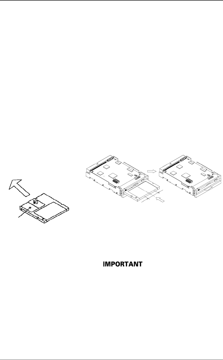
Operation and Cleaning
5-4 C156-E224-01EN
4) Push the cartridge into the slot until it completes moving below (a little
further in than the operator panel).
The cartridge remains inserted in the drive. The BUSY LED indicator lamp lights
when the drive power is turned on.
The cartridge remains inserted in the drive. Turning on the drive power starts
loading. (The LED indicator lamp should light.)
Notes
1) If the BUSY LED indicator lamp does not light when the power is turned
on, once eject the cartridge by pressing the eject button and insert it again
until the lamp is lit.
2) If the cartridge is inserted by pushing either left or right side of the
cartridge rear, it may not be inserted completely. Be sure to push the
central part straight into the drive until it is completely inserted.
3) If you attempt to insert the cartridge by force, trouble may result in the
drive. In such a case, be sure to once remove the cartridge and check the
insertion direction and the face and back of the cartridge before inserting
it again.
Inserting direction
Shutter
Push by hand the width of 20mm to the right and left from the
cartridge rear center, to the position shown at right.
Figure 5.2 Inserting cartridge
Even if you inserted the optical disk cartridge by pressing the left
side of the rear edge with the cartridge shutter surface facing
upward, and you heard a chucking sound, the device may not enter
the READY state. In such case, press the center of the rear edge of
the cartridge (check the dint part on the front side of the panel)
further, until the LED indicator lamp goes on. This lamp indicates
that the cartridge is normally inserted.

5.1 Operating Optical Disk Drive
C156-E224-01EN 5-5
5.1.4 Ejecting (removing) cartridge
Remove the cartridge as explained below.
(1) When the drive power is on:
The cartridge can be removed by pressing the eject button. (See figure 5.3)
Notes:
1) If the SCSI command prevents ejection, the cartridge cannot be removed.
2) Even if the drive set-up conditions are met, note that the cartridge can
drop from the drive after ejection depending on the ambient environment
and the cartridge's condition.
3) Remove the cartridge when completely ejected.
(2) When the drive power is off:
If the drive power is off, the cartridge cannot be removed by pressing the eject
button. The cartridge can be removed by insert the eject jig (accessory) or a pin
(diameter: about 1 mm) into the manual eject hole. (See figure 5.3)
Notes
1) NEVER attempt to eject the cartridge while the BUSY LED lamp is on.
The data may be destroyed or trouble may result in the drive.
2) Note that the cartridge may drop from the drive when it is ejected.
3) The optical disk drive unit should not be carried around with a cartridge
loaded inside.
Push the eject button
Figure 5.3 Removing cartridge

Operation and Cleaning
5-6 C156-E224-01EN
5.2 Cleaning Drive
When a dust or smoke of cigarette is stained to the lens actuator, a performance of
whole drive may be down. Clean the lens actuator periodically using following
head cleaner.
Note:
Cleaning period differs depending on the installation condition. Usually,
cleaning period is once a three months.
Table 5.1 Head cleaner
Part name Product number Order number
Head cleaner 020470 CA90002-C980
(1) Cleaning method
Clean the head actuator with following method.
1. Turn on the power of the drive.
2. Insert the head cleaner.
3. When the head cleaner is automatically loaded, the optical head positioner
moves back and forth and the cleaning brush mounted on the head cleaner
cleans the object lens.
4. When the cleaning is finished, the head cleaner is automatically unloaded.
(cleaning time: 15 seconds)
Device Damage: Be sure to use the dedicated head cleaner
described above.
Check the cleaning brush state by opening the shutter of the head
cleaner. If the tip of brush is open, use new head cleaner.
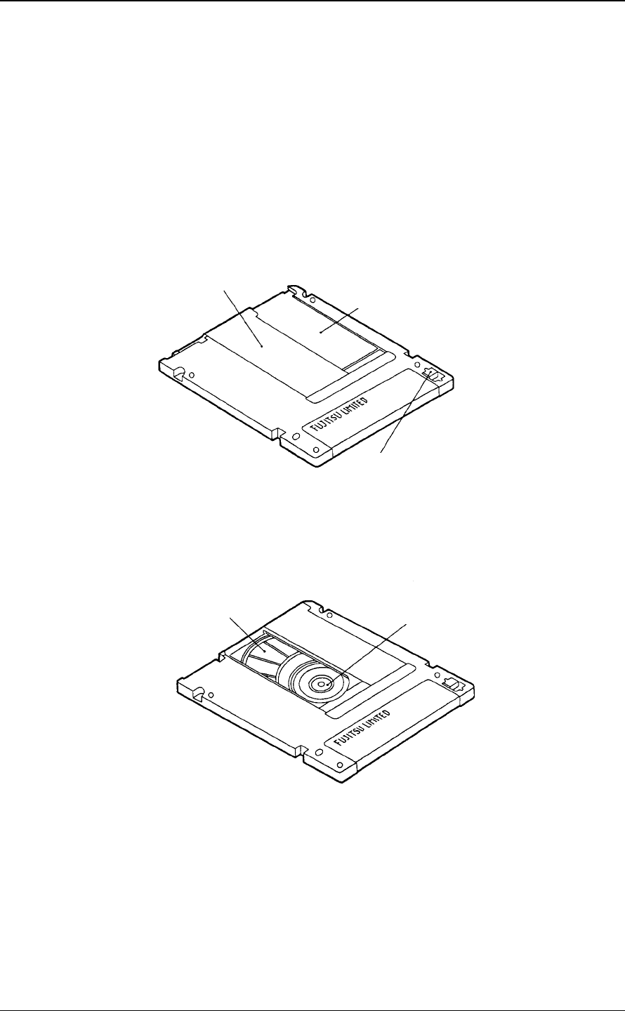
5.3 Optical Disk Cartridge Operation
C156-E224-01EN 5-7
5.3 Optical Disk Cartridge Operation
5.3.1 Optical disk cartridge
Figure 5.4 shows the optical disk cartridge. For operation and cleaning, users
should be familiar with the parts shown in the figure.
See Subsection 2.3.2 for the functions of the parts.
a. Shutter closed
b. Shutter open
Figure 5.4 Optial disk cartridge
3. Write protect tab
1. Cartridge case
2. Shutter
5. Hub
4. Disk
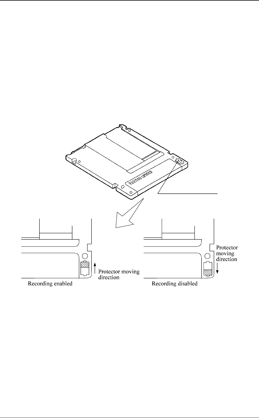
Operation and Cleaning
5-8 C156-E224-01EN
5.3.2 Write protect tab
Moving the write protect table determines whether to enable or disable writing of
the optical disk cartridge. Use a fingernail to move the write protect tab (it must be
completely moved to the end because there is play in the middle).
Figure 5.5 shows the write protect tab location on the optical disk cartridge and the
moving state of the write protect tab (see "write enabled" and write disabled"
enteredonthelabel).
Note:
The hatched part indicates the write protect tab location.
Figure 5.5 Write protect tab
Write protect tab
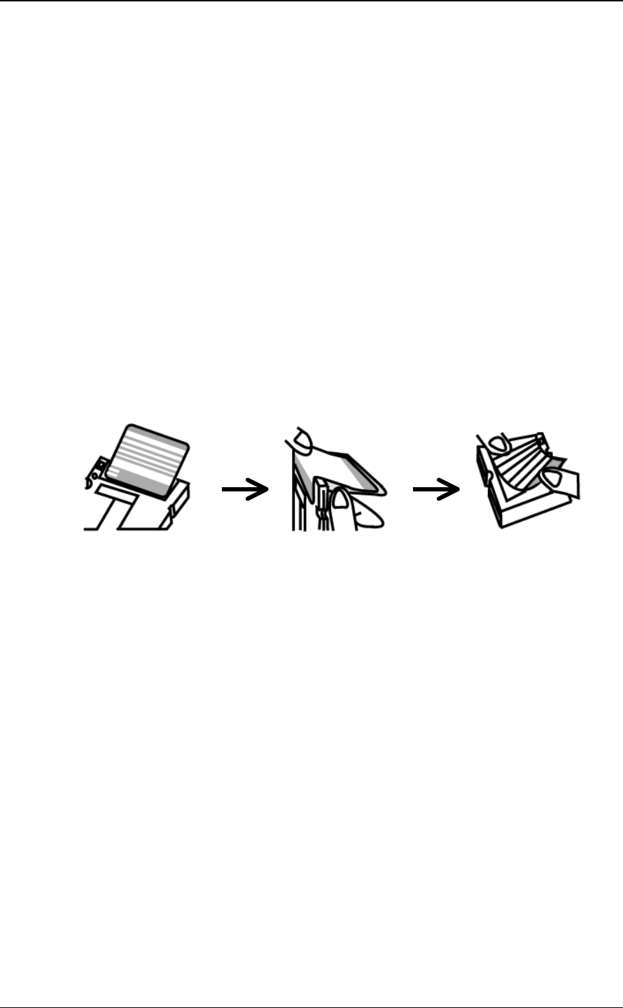
5.3 Optical Disk Cartridge Operation
C156-E224-01EN 5-9
5.3.3 How to affix an index label on the MO cartridge (See figure 5.6)
(1) Note the following when affixing an index label:
• Be careful not to let the label become misaligned.
• Be sure to prevent the formation of air bubbles or peeling.
(2) How to affix an index label
Follow the procedure below when affixing an index label. (See Figure 5.x.)
1) Clean the surface of the MO cartridge before affixing the index label.
2) For a better finish, start sticking the index label from the backside of the MO
cartridge.(a)
3) Once the backside is done, firmly press each corner of the index label.(b)
4) When the front is also complete, again press every corner of the index label to
prevent the label from coming off.(c)
(a) (b) (c)
Figure 5.6 How to stick an index label on the MO cartridge
5.3.4 Notes
To maintain the performance and reliability of the optical disk cartridge, keep the
following points in mind when using, storing, or transporting the cartridge:
(1) When using the cartridge:
• Do not use the cartridge where exposed to direct sunlight or where the
temperature changes sharply, the temperature is high, or the humidity is high.
• Do not apply excessive pressure to the cartridge case or shutter. Avoid
dropping the cartridge.
• Do not use the cartridge in a dusty or smoky place.
• Do not open the shutter or touch the disk surface.

Operation and Cleaning
5-10 C156-E224-01EN
(2) When storing the cartridge:
• Do not place a heavy objects on the cartridge.
• Do not store the cartridge where exposed to direct sunlight or where the
temperature changes sharply, the temperature is high, or the humidity is high.
• Do not store the cartridge in a dusty or smoky place.
(3) When transporting the cartridge:
• Put the cartridge in a nylon bag to protect it from moisture.
• Put the cartridge in a strong container and cover the cartridge with cushioning
material.

5.4 Cleaning Optical Disk Cartridge
C156-E224-01EN 5-11
5.4 Cleaning Optical Disk Cartridge
Dust or cigarette smoke particulates on the disk surface lowers the performance of
the cartridge. Regularly clean the disk. The cleaning frequency depends on the
drive installation environment. Determine how often the drive should be cleaned
in consideration of the environment. A standard of he cleaning period is every 300
hours usage or once a 2 to 3 months.
5.4.1 Cleaning tool
Use the cleaning kit to clean the disk cartridge.
(1) Cleaning kit
This cleaning kit is only for 3.5-inch optical disk cartridge. Use with reading the
attached operation guide well. Table 5.2 shows the order number of the cleaning
kit.
Table 5.2 Cleaning kit
Part name Product number Order number
Cleaning kit 0632440 CA90003-0702
Table 5.3 shows the packed items in the cleaning kit.
Table 5.3 Packed items (cleaning kit)
Name Contents
Setting case 1 piece
Cleaning cloth 5 pieces (70mm ×70mm)
Cleaning solution 1 bottle (20ml)
The following sub-kit is available as a set of the cleaning solution and cleaning
cloth as supplement.
• Product No. 0632450
• Order No. CA90002-D901
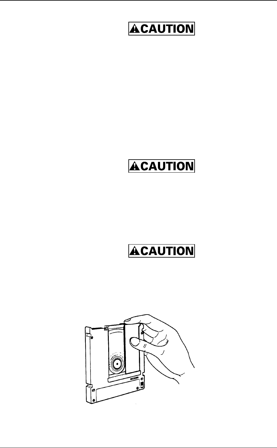
Operation and Cleaning
5-12 C156-E224-01EN
Damage for disk medium: Use the cleaning solution and
cleaning cloth specified in Table 5.2. If other than the specified
items is used, disk media surface may be damaged.
(2) Notes on usage and storage of cleaning kit
• When storaging the cleaning solution, tighten the cap.
• As the magnet is used at revolving knob of the setting case, do not place the
floppy disk near the revolving knob.
• Do not use or storage where exposed to direct sun light or near the
inflammables.
• Keep out of the reach of children.
Damage for data medium: Do not use this cleaning kit for the
floppy disk or the optical disk cartridge used for other optical disk
drive.
5.4.2 Cleaning procedure
Clean the disk cartridge with a following procedure.
Damage for disk medium: Clean the cartridge at clean place. Put a disposable
groves at cleaning so that the fingerprint does not put on the disk media
(recommendation).
1) Slide the shutter completely open. (See figure 5.7)
Figure 5.7 Cleaning procedure (1)
5.4 Cleaning Optical Disk Cartridge
C156-E224-01EN 5-13
2) Set the cartridge with keeping label side down and shutter open to the shutter
stopper of the setting case as shown in Figure 5.8.
Figure 5.8 Cleaning procedure (2)
Damage for disk medium: At setting the cartridge to the setting
case, do not apply the heavy shock and push hardly.
3) Cover the cartridge with the setting case cover, then insert the spindle pin into
the center hub of the cartridge.
Figure 5.9 Cleaning procedure (3)
4) Remove a slender piece that causes a defect from the disk surface at wiping
the disk media.
5) Moisten the cleaning cloth with a few drops of cleaning solution.
Shutter stopped
Setting case
Setting case as shown
Disk media
Spindle
Shutter
Cartridge
Cartridge opening
Disk media
Disk hub
Setting case cover
Revolver
Operation and Cleaning
5-14 C156-E224-01EN
Eye inflammation: In case of contact with eyes, immediately
flush eyes with water.
6) Wipe the disk surface from the hub outward.
7) Turn the revolving knob, then wipe the disk surface.
Figure 5.10 Cleaning procedure (4)
8) If the excess cleaning solution remains on the disk surface, wipe out with the
cleaning cloth.
Cleaning cloth

C156-E224-01EN 6-1
CHAPTER 6 Diagnosis and Maintenance
This chapter contains diagnosis and maintenance information.
6.1 Diagnosis
Table 6.1 shows a test executed by the diagnostic function.
The drive has a self-diagnostic function. This function can check the basic
operations of the drive.
A test program running in the host system is required to check general operations,
including operations of the interface with the host system. (See Subsection 6.1.3.)
Table 6.1 Self-diagnostic function
Diagnostic contents Target
Initial self diagnosis Basic operation
(hardware function test)
Diagnostic command Basic operation
Test program General operation
6.1.1 Initial self-diagnosis
When the power is turned on, the optical disk drive starts initial self-diagnosis.
Basic hardware functions are tested during initial self-diagnosis.
The hardware function test checks the normality of the basic controller operation.
This test includes the normality check of the ROM in which microcodes are
stored, microprocessor (MPU) peripheral circuit test, memory (RAM) test, and
data buffer test.
If an error is detected during initial self-diagnosis, the LED on the drive front
panel blinks.
6.1 Diagnosis
6.2 Maintenance Information

Diagnosis and Maintenance
6-2 C156-E224-01EN
6.1.2 Diagnostic command
The host system can make the ODD execute the self diagnosis by issuing the
EXECUTIVE DEVICE DIAGNOSTIC command. See Section 4.7.2,
"EXECUTIVE DEVICE DIAGNOSTIC", in details.
6.1.3 Test program
A test program running in the host system is required to check general operations
such as operations of the interface with the host system and simulated operations.
The configuration and function of the test program depend on the user system
requirements.
The test program should include the following tests:
(1) Random/sequential read test
Use the READ or VERIFY command to test positioning (seek) operation and read
operation in random access mode and sequential access mode.
(2) Write/read test
Use a disk whose operation check data may be destroyed so that a write or read
test can be executed with an arbitrary data pattern.

6.2 Maintenance Information
C156-E224-01EN 6-3
6.2 Maintenance Information
6.2.1 Maintenance requirements
(1) Preventive maintenance
No preventive maintenance is required.
(2) Service life
No overhaul is required within the first five years if the drive is used and handled
in an appropriate environment.
(3) Service system and repair
Fujitsu provides a service system and repair facility for its optical disk drive.
Submit information required to replace or repair the drive to your Fujitsu
representative. The following information should be included:
a) Optical disk drive model, part number (P/N), revision number, serial number
(S/N), and date of manufacture
b) Failure status
− Date of the failure
− System configuration
− Environment conditions (temperature, humidity, and supply voltage)
c) Failure history
d) Failure
− Description of the failure
− Issued commands and specified parameters
− Sense data
− Other error analysis information
Data loss:
In case of regular repair, the optical disk cartridge should not be
attached except where the cartridge causes the error. And before
having the drive repaired, save the data in the cartridge. Fujitsu is
not responsible for data lost during maintenance or repair.
See Section 5.3.3 for details on packing and handling the drive when sending it to
Fujitsu.

Diagnosis and Maintenance
6-4 C156-E224-01EN
6.2.2 Revision number
The revision number of an optical disk drive is represented with an alphabetic
character and a single-digit number. The revision number is shown on the revision
label attached to the drive. For example, Figure 6.1 shows the revision label
format.
Figure 6.1 Revision label
(1) Revision number indication
When the drive is shipped, the revision number is indicated by deleting the
numbers up to the corresponding number on the line of alphabetic characters.
(Each number is deleted with double lines =. See Figure 6.2.)
(2) Changing the revision number on site
When the revision number is changed on site because of parts replacement or
modification, the new revision number is indicated by circling the number on the
line of alphabetic characters. (See Figure 6.2.)
When a revision number is changed after shipment, Fujitsu issues
"Revision Number Change Request/Notice" to indicate the new
revision number. The user must update the revision label as
described above when changing the revision number.
Revision number indicated on shipment
REV. NO. A 0 1 2 3 4 5 6 7 8 9 ! Revision A2
Revision number changed on side
REV. NO. A 0 1 2 3 4 5 6 7 8 9 ! Revision A3
Note: The "A" of the Revision Number is a stamp.
Figure 6.2 Revision number indication
Revision number

C156-E224-01EN GL-1
Glossary
Axial acceleration
Acceleration on the recording layer along with the line perpendicular to the disk
reference surface to a specified rotation speed. Axial acceleration is detected by
optical means.
Axial displacement
A displacement at a point on the recording layer in a direction perpendicular to
the disk reference surface from its original standard position. The standard
position on the recording layer is detected optically using the thickness of the
protective layer and refraction rate based on the disk reference surface.
Case
A cover of the optical disk. The case protects the disk from being damaged
during handling and also allows the operator to exchange disks easily. The case
also contains a label, write protection tab, automatic handling support, and media
identification hole.
CDB (Command Descriptor Block)
A series of data describing input-output commands. CDB is sent from the
initiator to the target.
Clamp area
A ring area on the disk on which a clamp force is applied by the clamp
mechanism.
Command
An input-output instruction to the target. Described as CDB.
Control track
A track used to store media parameters and format information required to record
and read data to or from the optical disk.
Defect management
In real time, an automatic program used to change the power, focus, tracking of
reading and recording if an error is detected and to decide if many error sectors
should be discarded. In batch mode, a guideline used to re-record or save the
disk.

Glossary
C156-E224-01EN GL-2
Disk reference surface
An ideal flat ring surface of an ideal spindle that is in contact with the clamp area
on the disk. It is perpendicular to the rotation axis.
Error correction code
An error correction code designed to correct specific errors in data.
Error detection and correction
A series of data by adding a redundant code to data in the existing format. In read
mode, the decoder removes a redundant code and detects and corrects errors using
redundant information.
Interleaving section
A process that physically arranges data units so that data resists burst errors.
LUN (Logical Unit Number)
A device address used to identify a logical unit.
Recording layer
A layer on the disk on which data is recorded at production or recording .
Recording power
An incidence power specified on the incidence surface. Used to form marks.
Sense code
A single-byte code set in sense data. This information is used to determine the
type of error detected.
Sense data
Information generated by the target to report detailed error information if any
error information is contained in the command end status.
Sense key
A 4-bit code set in sense data. This information is used to classify the type of
error detected.
Spindle
A component of the disk drive unit that is in contact with the disk and hub.

Glossary
C156-E224-01EN GL-3
Status
A single-byte information reported from the target to the initiator at the end of
each command execution. The status indicates the end status of a command.
This page is intentionally left blank.

C156-E224-01EN AB-1
Acronyms and Abbreviations
A
AC Alternating Current
ACK ACKnowledge
ALPG Automatic Laser Power Control
AM Address Mark
ANSI American National Standards
Institute
ARRE Automatic Read Reallocation
Enabled
ASC Additional Sense Code
ASCII American Standard Code for
Information Interchange
ASCQ Additional Sense Code Qualifier
ATN ATteNtion
AWG American Wire Gauge
AWRE Automatic Write Reallocation
Enabled
B
BCV Buffer Control Valid
BPV Bit Pointer Varid
BSY BuSY
BytChk Byte Check
C
C/D Control/Data
CCS Common Command Set
CDB Command Descriptor Block
CDRH Center for Devices and
Rediological Health
CRC Cyclic Redundancy Code
CSA Canadian Standards Association
D
DB Data Bus
DBD Disable Block Descripter
DBP Data Bus Parity
DC Direct Current
DCRT Disable CeRTification
DDS Disk Definition Sector
DMA Defect Management Area
DPO Disable Page Out
DPRY Disable PRimarY
DSP Digital Signal Processor
E
EBC Enable Blank Check
EBP Erase By-Pass
ECC Error Correction Code
EN European Norm
EVPD Enable Vital Product Data
F
FG Frame Ground
FIFO First In First Out
FmtData Format data
FOV Format Options Valid
FRU Field Replaceable Unit
G
GND Ground
I
I/O Input/Output
IC Integrated Circuit
ID IDentifier
IDD Intelligent Disk Drive
IEC International Electrotechnical
Commission
Immed Immediate
IP Initialize Pattern
ISO International Standardization
Organization
L
LD Laser Diode
LED Light Emitting Diode
LoEj Load Eject
LSB Least Significant Byte
LUN Logical Unit Number
M
MPU MicroProcessor Unit
MSB Most Significant Byte
MSG MeSeaGe
MTBF Mean Time Between Failures
MTTR Mean Time To Repair

Acronyms and Abbreviations
C156-E224-01EN AB-2
N
N.C. No Connection
O
ODD Optional Disk Drive
ODF Offset Detection Flag
OEM Original Equipment Manufacturer
P
PA PostAmble
P/N Part Number
PC Page Control
PCA Printed Circuit Assembly
PCF Page Control Field
PCR Parameter Code Reset
PDL Primary Defect List
PEP Phase Encoded Part
PF Page Format
PLL Phase-Locked Loop
PMI Partial Medium Indicator
PPC Parameter Pointer Control
PWM Pulse Width Modulation
R
RAM Random-Access Memory
RelAdr Relative Addressing
REQ REQuest
RH Relative Humidity
ROM Read only Memory
rpm revolutions per minute
RST ReSeT
RSV ReSerVed
S
S/N Serial Number
SB Spare Band
SCT SeCTor
SDL Secondary Defect List
SDTR Synchronous Data Transfer
Request
SEL SELect
SFP Standard Formatted Part
SG Signal ground
SKSV Sense Key Specific Valid
SM Sector Mark
SNSKEY SeNSe KEY
SP Save Page
SP Save Parameter
STPF SToP Format
SYNC SYNCronization mark
T
TTL Transister-transister-logic
Typ Typical
U
UB User Band
UL Underwriters Laboratories
Incorporated
V
VCM Voice coil motor
VDE Verband Deutscher
Elektrotechniker
VFO Variable Frequency Oscillator
VLD VaLiD
VPD Vital Product Data
VU Vendor Unique

Fujitsu Internal Use Only
C156-E224-01EN IN-1
Index
128 MB disk 2-9
1.3 GB disk 2-9
230 MB disk 2-9
2.3 GB capacity 1-2
2.3 GB disk 2-9
540 MB/640 MB disk 2-9
A
ABORT message 4-43
active mode 4-6
actuator section 1-9
adaptability 1-4
air flow 3-3
air purity 3-4
algorithm for alternate processing 2-11
allowable input voltage and current 3-11
ARBITRATION phase 4-50
ASC and ASCQ definition 4-29
ATTENTION condition 4-54
automatic allocation of alternate data block
1-4
automatic alternate sector assignment
function 4-4
automatic spindle stop function 1-3
B
bit 2 to 0 4-44
bit 6 4-44
bit error rate after ECC processing 2-5
Block Descriptor 4-23
block descriptor 4-15
Bus Device Reset 4-4
BUS DEVICE RESET message 4-44
BUS FREE phase 4-49
C
cable connection 3-12, 3-25
cable connector specification 3-15
cache function 4-4
Caching page 4-19
cartridge case 2-9
CDB of READ (6) command 4-32
CDB of WRITE (10) command 4-33
center of gravity 3-8
changing revision number on site 6-4
check before mounting drive 3-24
check if error occurs at initial self-diagnosis
3-26
cleaning drive 5-6
cleaning kit 5-11
cleaning optical disk cartridge 5-11
cleaning procedure 5-12
cleaning procedure (1) 5-12
cleaning procedure (2) 5-13
cleaning procedure (3) 5-13
cleaning procedure (4) 5-14
cleaning tool 5-11
COMMAND COMPILE message 4-43
compatible with international standard
(media interchangeability) 1-3
configuration 1-8
confirming initial operation 3-26
conformance to SCSI-2 1-5
connecting more than one ooptical disk drive
(multi-host) 3-17
connecting more than one optical disk drive
(single host) 3-16
connecting one optical disk drive 3-16
connection check 3-27
connection mode 3-16
connector and terminal location 3-12
continuous block processing 1-5
control circuit section 1-10
control circuit section block diagram 1-10
controller circuit section 1-10
current waveform (+5 VDC) 3-11
current waveform (reference) 3-11
D
data buffer 1-5, 4-5
data security at power failure 2-6
default jumper setting 3-18
default value in Caching page 4-19
default value in flexible disk page 4-18
default value in Power condition page 4-20
default value in read-write error recovery
page 4-16
default value in Verify control page 4-21
defect descriptor 4-39
defective block slipping 1-6
defective sector management 4-4
Defect List Format of READ DEFECT
DATA (10) command 4-38
Defect List Header 4-37
defect list header of READ DEFECT DATA
(10) command 4-38
defect management 2-11

Index Fujitsu Internal Use Only
IN-2 C156-E224-01EN
defect management schematic diagram 2-11
device driver software 1-6
diagnosis 6-1
diagnosis and maintenance 6-1
diagnostic command 6-2
diagnostic function 1-4
dimension (without panel) 3-6
direct-overwrite medium support 1-3
DISCONNECT message 4-43
disk 2-9
disk specification 2-9
dismounting drive 3-27
drive circuit section 1-10
drive configuration 1-7
drive connector 3-12
drive model 1-7
drive specification 2-2
dust resistance 1-3
E
ejecting (removing) cartridge 5-5
environmental and power requirement 2-4
environmental requirement 3-1
ERASE command 4-36
Error Code 4-27
error rate 2-5
error recovery 1-3
example of alternate processing 2-12
external dimension 3-5
external light source 3-10
external magnetic field 3-10
F
FAST SCSI timing specification 4-49
feature 1-2
five-year service life (no overhaul) 1-4
flexible disk page 4-17
format progress indication byte 4-30
FORMAT UNIT command 4-37
FORMAT UNIT parameter list 4-37
G
general description 1-1
general notes 3-21
H
half-height standard 90 mm (3.5-inch) size
1-2
head cleaner 5-6
high-speed data transfer 1-2
high-speed mean seek time 1-3
host interface 4-1
how to affix index label 5-9
how to affix index label on MQ cartridge
5-9
hub 2-9
I
IC (controller, read amp) 3-2
IDENTIFY message 4-44
idle mode 4-7
if processing terminates abnormally 3-27
initial operation when power is turned on
3-26
initial self-diagnosis 6-1
INITIATOR DETECTED ERROR message
4-43
INQUIRY 4-11
INQUIRY command 4-11
INQUIRY command response data 4-12
inserting cartridge 5-3, 5-4
inside optical disk cartridge 3-2
installation 3-22
installation direction 3-7
installation requirement 3-1
interface 1-5
interface connector 4-1
L
leak magnetic field 3-10
LED indication 4-8
location of setting terminal 3-12
logical track address format 4-28
lower power consumption 1-3
M
maintenability 1-4
maintenance information 6-3
maintenance requirement 6-3
mechanical section 1-9
message format 4-42
message function 4-43, 4-44
MESSAGE PARITY ERROR message
4-44
MESSAGE REJECT message 4-44
message type 4-42
model 2-1
Mode Page 4-24
mode page 4-15
mode page code 4-14
mode parameter 4-23
Mode Parameter Header 4-23
mode parameter header 4-14
mode parameter list 4-14

Fujitsu Internal Use Only Index
C156-E224-01EN IN-3
MODE SELECT command 4-13
MODE SENSE command 4-22
mounting 3-24
mounting frame structure 3-9
mounting frame structure and clearance 3-9
mounting procedure 3-24
mounting requirement 3-5
MO write cache 4-6
MTBF 1-3, 2-6
N
NO OPERATION message 4-44
note 5-3
note following when affixing index label
5-9
notes 5-9
notes on drive handling 3-21
notes on mounting 3-9
notes on usage and storage of cleaning kit
5-12
O
operability 1-4
operating optical disk drive 5-1
operation and cleaning 5-1
operation confirmation and preparation for
use after installation 3-26
optical disk cartridge 2-8, 5-7
optical disk cartridge load/eject 1-9
optical disk cartridge operation 5-7
optical disk cartridge specification 2-7
optical disk drive 5-2
optical disk drive configuration 1-8
optical disk drive front view (with panel)
5-2
optical disk drive specification 2-1
outer view (without panel) 1-7
outer view (with panel) 1-7
P
packed item (cleaning kit) 5-11
packing 3-22
packing style 3-23
page control field 4-22
panel 1-9
panel function processing 3-10
performance 1-1
pin assignment 3-14
postioning error rate 2-5
Power condition page 4-19
power management function 4-6
power mode 4-6, 4-8
power mode transition 4-8
Power-On Reset 4-4
power-on reset 4-4
power supply requirement 3-11
pre-idle mode 4-7
PREVENT/ALLOW MEDIUM REMOVAL
command 4-31
preventive maintenance 6-3
product number 2-1
R
random/sequential read test 6-2
READ (10) command 4-32
READ (6) command 4-32
read-ahead cache feature 1-5
read cache 4-5
READ CAPACITY command 4-13
READ CAPACITY data 4-13
READ DEFECT DATA command 4-38
READ LONG command 4-41
read/write error recovery page 4-15
RECEIVE DIAGNOSTIC RESULTS
command 4-39
recommended component for connection
3-15
recommended optical disk cartridge
specification 2-7
RELEASE command 4-26
reliability 1-3, 2-6
REQUEST SENSE command 4-26
Request Sense Data 4-27
RESELECTION phase 4-51
RESERVE command 4-25
reset response 4-4
response to Prevent, Allow, and Eject 4-31
revision label 6-4
revision number 6-4
revision number indication 6-4
S
safety standard 1-4
SAVE DATA POINTER message 4-43
SCSI bus connection mode 3-16
SCSI command 4-10
SCSI commands 4-10
SCSI ID 3-18
SCSI ID setting (CNH2) 3-18
SCSI interface connector (cable side) 4-2
SCSI interface connector (ODD side) 4-1
SCSI interface connector pin assignment
(single-ended type) 4-3
SCSI message 4-42
SCSI Reset 4-4

Index Fujitsu Internal Use Only
IN-4 C156-E224-01EN
SCSI terminating resistor mode 3-19
SCSI terminating resistor mode (CNH1)
3-19
sector address format 4-39
SEEK (10) command 4-35
SEEK (6) command 4-35
SELECTION phase 4-51
self-diagnostic function 6-1
SEND DIAGNOSTIC command 4-39
Sense Key 4-28
separator optical section 1-9
service clearance 3-10
service life 2-6, 6-3
service system and repair 6-3
setting 3-18
setting terminal 3-18
setting terminal (CNH2) 3-18
shape of setting terminal 3-13
shutter 2-9
shutter closed 2-8, 5-7
shutter open 2-8, 5-7
specification 2-1
spindle motor 1-9
standby mode 4-7
standby timer 4-7
start, stop and eject processing 4-24
START/STOP UNIT command 4-24
storage 3-23
surface temperature measurement point 3-2
SYNCHRONIZE CACHE command 4-36
SYNCHRONOUS DATA TRANSFER
REQUEST message 4-44
system ground 3-11
T
temperature at each measuring point
(reference) 3-4
temperature measurement point 3-1
temperature requirement and measuring
method 3-3
temperature requirement at measurement
point 3-3
temperature rise under several conditions
3-4
test program 6-2
TEST UNIT READY command 4-11
timing rule 4-46
timing specification 4-46
transfer in asynchronous mode 4-52
transfer in FAST SCSI mode 4-53
transfer mode setting requested by INIT to
ODD 4-45
transportation 3-23
type of message provided by ODD 4-42
U
unpacking 3-21
V
variable value in Caching page 4-19
variable value in flexible disk page 4-18
variable value in Power condition page
4-20
variable value in read-write error recovery
page 4-16
variable value in Verify control page 4-21
various process 4-4
various radio wave standard 1-4
VERIFY command 4-33
Verify control page 4-20
Verify mode 4-21
vibration resistance (shock resistance) 1-4
W
when drive power is off 5-3, 5-5
when drive power is on 5-3, 5-5
when storing cartridge 5-10
when transporting cartridge 5-10
when using cartridge 5-9
wide operating environment 1-4
WRITE (10) command 4-34
WRITE (6) command 4-33
WRITE AND VERIFY 4-34
WRITE AND VERIFY command 4-34
WRITE BUFFER command 4-40
write cache feature 1-5
write cache mode 3-19
write cache mode setting 3-19
WRITE LONG command 4-41
write protect tab 2-9, 5-8
write/read test 6-2
Comments concerning this manual can be directed to one of the following addresses:
FUJITSU LIMITED
Storage Product Group
4-1-1, Kamikodanaka, Nakahara-ku, Kawasaki
211-8588, Japan
TEL: 81-44-754-8350
FAX: 81-44-754-8351
FUJITSU COMPUTER PRODUCTS OF AMERICA, INC.
2904 Orchard Parkway, San Jose,
California 95134-2009, U.S.A.
TEL: 1-408-432-6333
FAX: 1-408-894-1709
FUJITSU CANADA INC.
2800 Matheson Blvd. East, Mississauga, Toronto,
Ontario L4W 4X5, CANADA
TEL: 1-905-602-5454
FAX: 1-905-602-5457
FUJITSU EUROPE LIMITED
Hayes Park Central
Hayes End Road
hayes UB4 8FE, U.K.
TEL: 44-20-8573-4444
FAX: 44-20-8573-2643
FUJITSU DEUTSCHLAND GmbH
Frankfurter Ring 211, 80807 München, GERMANY
TEL: 49-89-323780
FAX: 49-89-32378100
FUJITSU NORDIC AB
Kung Hans Väg 12, S-192 68 Sollentura, SWEDEN
TEL: 46-8-626-6000
FAX: 46-8-626-6711
FUJITSU ITALIA S.p.A.
Via Nazario Sauro, 38 20099 Sesto S. Giovanni (MI), ITALY
TEL: 39-2-26294-1
FAX: 39-2-26294-201
FUJITSU FRANCE S.A.
1, Place des Etas-Unis, SILIC 310,
94588 Rungis Cedex, FRANCE
TEL: 33-1-41-80-38-80
FAX: 33-1-41-80-38-66
FUJITSU ICL ESPAÑA S.A.
Almagro 40, 28010 Madrid, SPAIN
TEL: 34-91-581-8000
FAX: 34-91-581-8300
FUJITSU AUSTRALIA LIMITED
2 Julius Avenue (Cnr Delhi Road) North Ryde N.S.W. 2113,
AUSTRALIA
TEL: 61-2-9776-4555
FAX: 61-2-9776-4556
FUJITSU HONG KONG LTD.
10/F., Lincoln House, 979 King's Road, Taikoo Place, Island
East, Hong Kong
TEL: 852-2827-5780
FAX: 852-2827-4724
FUJITSU KOREA LTD.
Coryo Finance Center Bldg, 23-6, YoulDo-Dong,
Young DungPo-Gu, Seoul, Republic of KOREA
TEL: 82-2-3787-6000
FAX: 82-2-3787-6029
FUJITSU COMPUTERS (SINGAPORE) PTE. LTD
20 Science Park Road #03-01,
TELETECH PARK SINGAPORE SCIENCE PARK II,
Singapore 117674
TEL: 65-777-6577
FAX: 65-771-5669
FUJITSU TAIWAN LTD.
8F, Hun Tai Center, 168-170, Tun Hwa North Road,
1st Sec., Taipei, TAIWAN
TEL: 886-2-545-7700
FAX: 886-2-717-4644
FUJITSU SYSTEMS BUSINESS (THAILAND) LTD.
12th F1., Olympia Thai Tower, 444 Rachadapisek Road,
Samsennok, Huay Kwang, Bangkok 10320, Thailand
TEL: 66-2-512-6066
FAX: 66-2-512-6068
This page is intentionally left blank.

FUJITSU LIMITED
READER’S COMMENT FORM
Your comments or suggestions on this document are cordially solicited. For any comments and suggestions
you may have, please complete and submit this form to your FUJITSU representative. The comments and
suggestions will be used in planning future editions. Thank you for your cooperation.
Date issued: Manual name:
Name: Manual code:
Company or organization:
Address:
Comments:
Page Line Comments
Reply requested: Yes No
Please evaluate overall quality of this manual by marking (√) in the appropriate boxes.
Good Fair Poor Good Fair Poor Good Fair Poor
Organization: Use of examples: Legibility:
Accuracy: Index coverage: Handiness/Binding:
Clarity: Cross referencing: (Others):
Figures & tables: General appearance:
Technical level: Too high Appropriate Too low
Overall rating of
this publication: Good Fair Poor
FOR FUJITSU USE
Overseas office: Person in charge:
Note) Local representative should pass this form to the section in charge of distribution in FUJITSU.
Reply
MCJ3230SS OPTICAL DISK
DRIVE PRODUCT MANUAL
C156-E224-01EN
By