Fujitsu Wafer Level Packaging (Super CSP) Supercsp
User Manual: Fujitsu Wafer Level Packaging (Super CSP) Packaging ation - Fujitsu United States
Open the PDF directly: View PDF ![]() .
.
Page Count: 3
17 Fujitsu Microelectronics America, Inc.
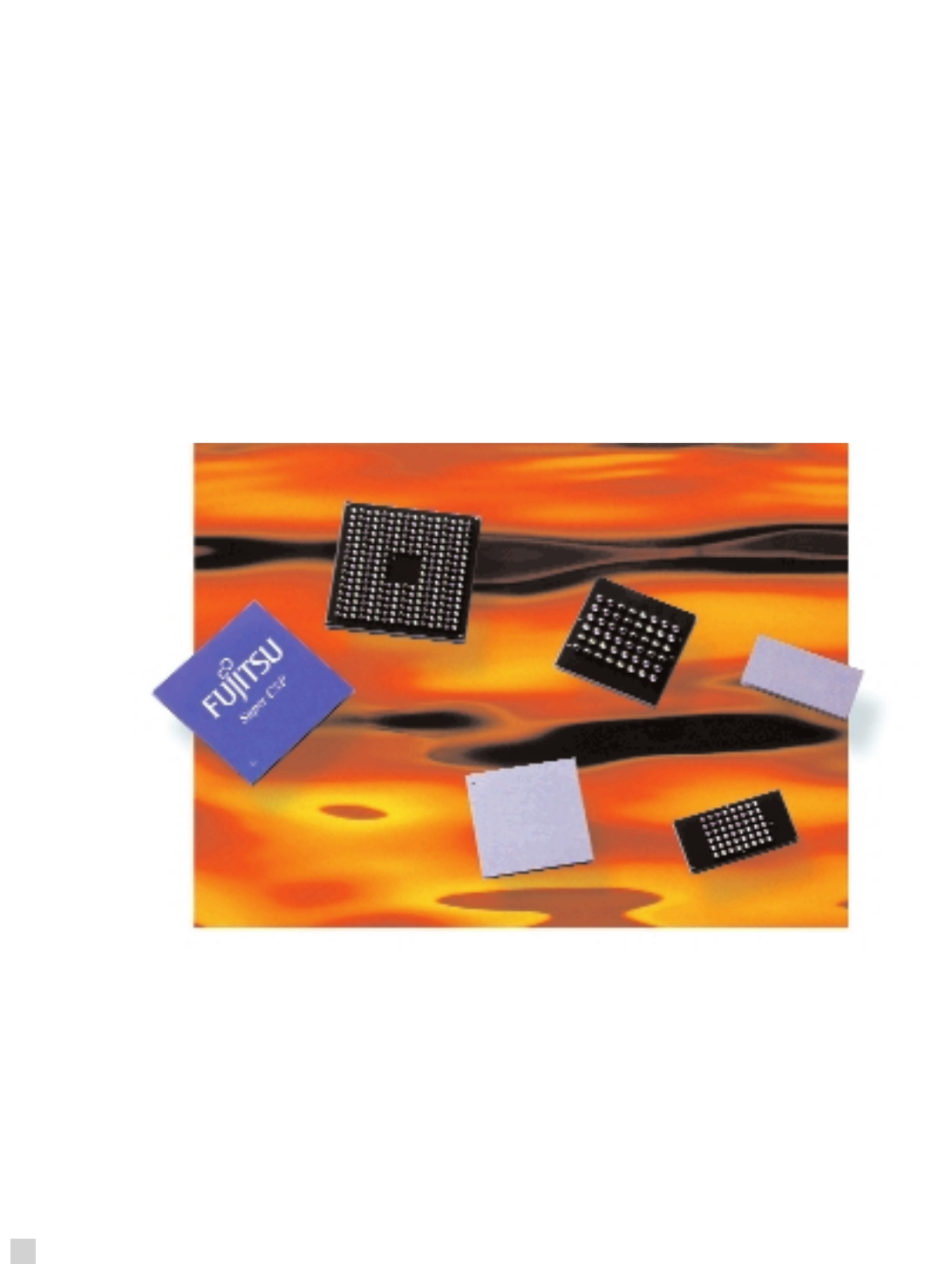
Super Chip Scale Package (SCSP) is a wafer level package that is a true chip size package. It
provides a potential solution for “known good die”, or one test point operation as compared to
two. In single chip packaging, it is customary to have testing at the wafer probe and again after
packaging.
This package is ideal for low to mid range pin count applications, such as FLASH memory, ASIC
and System on Chip (SOC). Board level reliability is excellent due to the use of flexible copper
posts and modified epoxy resin, as well as CTE close to that of the motherboard. Underfill is not
required as the epoxy resin provides a barrier to the alpha particle radiation.
• True Chip Size Package (CSP)
• No underfill required
• Wafer level processing
• Improved reliability and performance
• Cost effective
Super CSP

18
Advanced Packaging Services
Super CSP

19 Fujitsu Microelectronics America, Inc.
Super CSP
Temperature cycle* -65°C ~ 150°C 500 cycles Pass
Pressure cooker +121°C/85%RH 1000 hours Pass
HTS +150°C 500 hours Pass
Moisture sensitivity JEDEC Level 1 Pass
Test item Condition Cycle Result
Package Reliability (SCSP 48)
* Precondition: PB (+125°C/24 hours) + 85°C/85%RH/48 hours + IR reflow (+240°C peak)
Fabrication Flow
Standard Package Line-up
BGA48 3.51 x 7.05 x 1.00 0.5 6 x 8
LGA48 3.51 x 7.05 x 0.75 0.5 6 x 8
LGA48 4.70 x 5.32 x 0.75 0.5 6 x 8
LGA92 5.51 x 5.63 x 0.75 0.4 3 11 x 11
LGA240 8.20 x 8.20 x 0.75 0.4 4 19 x 19
LGA300 9.00 x 9.00 x 0.75 0.4 5 20 x 20
Custom configurations are available upon request.
Package Type Body Size Pitch Solder Ball
(mm) (mm) Row Matrix
