User Manual
MDS LN100 Integrator’s Guide 05-6950A01, revision 3
[1]
MDS LN100 Integrator’s Guide
1.0 INTRODUCTION
The LN100 (Figure 1), is a fixed location (not intended for mobile use), multi-modem system operating in licensed
bands between 150-174, using channel bandwidths of 6.25kHz, 12.5kHz, and 25.0kHz. Modulation choices for each
bandwidth include CPFSK, QPSK, 16QAM, and 64QAM. Maximum power and modem speed is based on frequency,
modem choice, and applicable emission mask.
The unit is designed for use inside data equipment to provide reliable connectivity in wireless networks. The LN100
power control circuit ensures that the RF output is linear and never exceeds +41.4 dBm at the antenna connector.
The module is designed for OEM use only. Host systems must be professionally installed. Host systems must be
factory configured by the OEM to operate at the correct frequency and output power setting. Refer to the table at the
end of this guide to determine applicable antenna types and the RF output power allowed.
1.1 Transceiver Features
The LN100 maximizes performance and flexibility in wireless networks, offering the following key features:
Selectable frequency (150-174MHz)
Selectable bandwidth (6.25kHz, 12.5kHz, 25.0kHz)
Selectable modem choices (CPFSK, QPSK, 16QAM, 64QAM)
RSSI and EVM readback indicators
Store-and-Forward repeater operation
Same hardware for Master, Remote, or Store-and-Forward configurations
Supports RS/EIA-232(TTL), Ethernet, and USB user interfaces
Operates at 5.25 Vdc at the MiniPCIe card edge power connections and 10-60Vdc at the 3-pin power
connector.
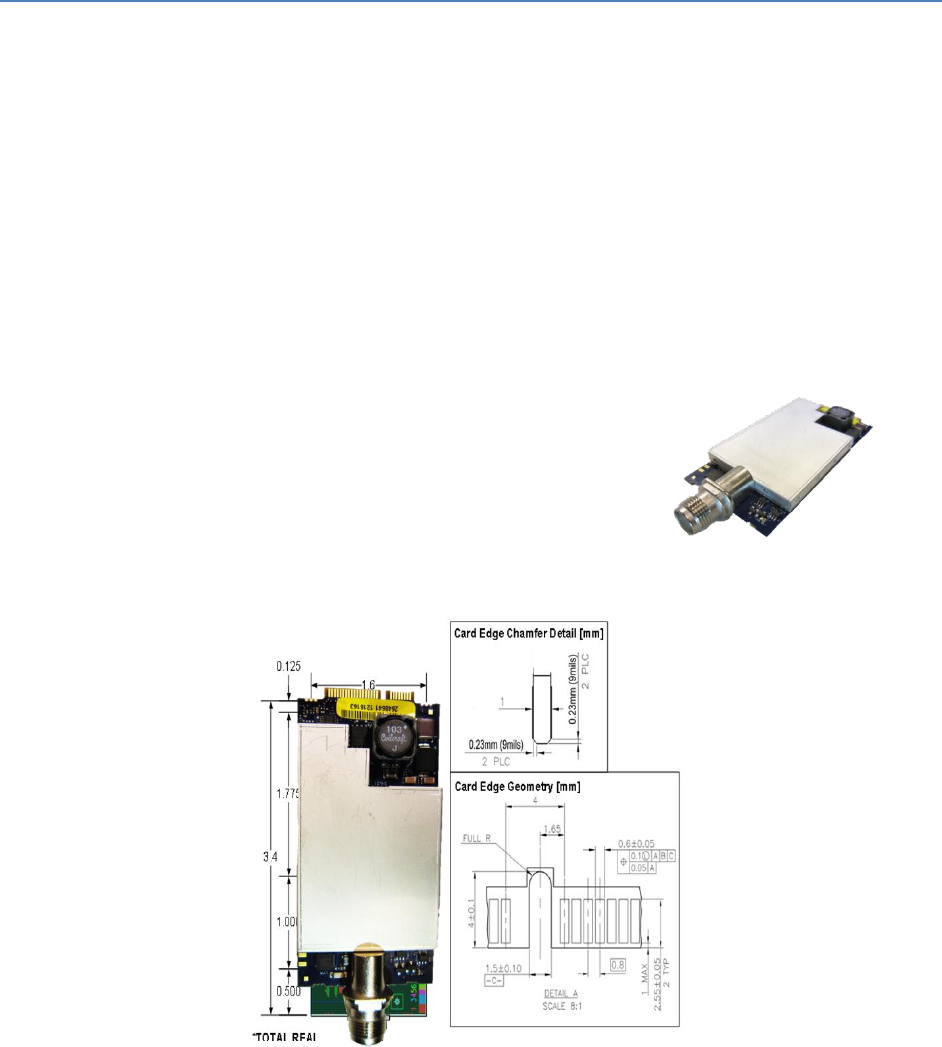
Figure 1. LN100 Transceiver Module
(Mini PCI-Express Card Edge for Data/Power/& I/O and J700 Antenna)
NOTE: Some features may not be available on all units, based on the options purchased, or regulatory constraints in
the country of operation.
MDS LN100 Integrator’s Guide 05-6950A01, revision 3
[2]
2.0 INSTALLATION
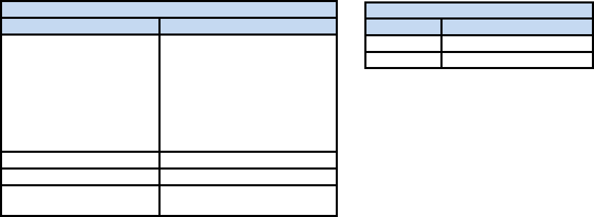
The transceiver is designed for installation in existing electronic equipment. The I/O and 5.25v power connections are
made through the Mini PCI-Express card edge. The 10-60v power is provided through a separate 3-pin connector on
the bottom of the module. The transceiver mounts to the host heatsink assembly using two #4 screws inside the RF
can area. The required heatsink contact area on the bottom surface of the PCB has the solder mask removed for
proper heat transfer.
Only one cable connection is required to the radio for the J700 Antenna connector. The module has three optionally
populated status LEDs (CR100, CR101, and CR1000) that indicate operating mode details. These LEDs provide
important information that is useful during startup and optimization of the radio link.
Antennas used with the radio can be either a Yagi directional type (often used at remote sites) or an omni-directional
type used for short range applications or at Master stations. Contact your sales representative for information on
available antennas.
Follow these steps to install the transceiver module:
1. Power down the Host assembly the module is being installed in to.
2. Mate the MiniPCIe card edge of the module into the socket on the Host assembly.
3. Secure the module to the heatsink surface using two #4 screws through the mounting holes in the corners of
the RF can area on the radio’s PC board.
4. Install the RF shield over the transceiver section.
5. Select and install an appropriate antenna and feedline for your system coverage requirements.
6. Connect the antenna coaxial lead to J700 on the module. It accepts a Type-TNC male coaxial connector.
7. Host Power Supply Requirements:
a. Input power applied on the 52-pin connector (J1100) must be a regulated 5.25 Vdc (-/+0.05 V).
b. Input power applied on 3-pin connector (J900) must not exceed the range 10.0-60.0Vdc
i. Nominal Input power on J900 is in the range 12-52Vdc - FCC CFR 47 2.1055(d)(1)
See Table 1 for power supply interface connections.
52-Pin GE MDS NIC Card Edge
Pin
Description
1, 6, 7, 10, 11, 13, 12, 14,
16, 19, 20, 23, 25, 28, 30,
31, 32, 33, 36, 38, 42, 44,
45, 46, 47, 48, 49, 51
GPIO
(Includes Ethernet &
Serial)
*Consult Factory
Documentation for
specific details
2, 24, 39, 41, 52
+5.25V
3, 5, 8, 17, 22
NC
4, 9, 15, 18, 21, 26, 27,
29, 34, 35, 37, 40, 43, 50
GND
Table 1. LN100 Power Supply Connections
3-Pin GE MDS (J900) connector
Pin
Description
1
GND
2, 3
+10.0-60.0V

MDS LN100 Integrator’s Guide 05-6950A01, revision 3
[3]
8. Set the radio’s basic configuration with a PC terminal through the Host system. The four essential settings
for all transceivers are (See Section 3 for commands):
Frequency
Bandwidth
Modem
Power
9. In a normally operating system, you will see the CR101 POWER LED turn on at start-up.
10. Optimize the installation by checking:
Antenna aiming and RSSI check
Optimal modem rate setting
3.0 RADIO PROGRAMMING
There are no manual adjustments on the radio. All programming and control is performed through a PC connected to
the Host platform that interfaces with the radio’s J1100 MiniPCIe card edge connector.
3.1 User Commands
The following tables provide descriptions of the various user commands for the transceiver.
Command
Description
Notes
ABOUT
Displays NIC version build time and
date.
HELP
Displays all available commands.
RESET
Software reset.
SER
Display the NIC serial number.
MODEM
Display/set NIC modem selection.
[4QAM, 16QAM, 64QAM]
BAUD
Display/set NIC symbol baud rate
selection.
[4800,9600,10000,16000,20000]
TEST ADDR
Read/write test address.
[0-7] Address used for tests (e.g. PER)
TEST PER
Starts a Packet Error Rate Test.
[-a] Destination test address
[-n] Number of packets to send
[-l ] Length of each packet
UPTIME
Display the amount of time since last
power cycle.
MDM KEY
Transmits un-modulated CW
MDM KEYR
Transmits modulated random data
MDM KEYLO
Transmits pass through of LO through
TX chain
MDM DKEY
Disables active transmission
MDM PRBURST
Transmits a modulated random data
burst of 511 bytes, useful for training
the receiver equalizer
MDM RSSI!
Instantaneous RSSI reading
dB
TX [val]
Read/write TX frequency
[val] - frequency in MHz
RX [val]
Read/write RX frequency
[val] - frequency in MHz
TCXO [arg1]
Change TCXO tuning voltage
[arg1] - Tuning voltage in V
TCXO CAL [arg1]
Calibrate TCXO tuning voltage
[arg1] - Tuning voltage in V
Table 2. LN100 User Commands
MDS LN100 Integrator’s Guide 05-6950A01, revision 3
[4]
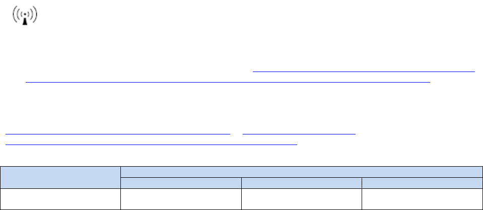
4.0 DC INPUT REQUIREMENTS
4.1 Power Consumption Ratings
The module has the following nominal power consumption ratings when operated at the required (V_NIC) input
voltage of 5.25 Vdc (-0.05/+0.05 V tolerance) and the required secondary input voltage of 10.0-60.0 Vdc on J900:
Active Receive Mode: 130mA
Transmit Mode (Worst Case Load): 1.3 Amperes
Power Regulation must be met by OEM to satisfy LMA conditions:
OEM Integrator should consult with Product Support for individual circuit implementations. The input voltage on the 3-
pin J900 connector accepts a wide range and routes to onboard regulator on the LN100 module, but the V_NIC input
on the 52-pin connector must be carefully regulated.
At minimum, OEM Integrators must regulate the DC voltage applied to +5.25 Vdc (V_NIC), with a tolerance
of -0.05/+0.05 Vdc. This can be achieved using a voltage regulator similar to the Texas Instruments LMR12020,
which is a precision DC regulator. The external +5.25 Vdc input is connected via pins 2, 24, 39, 41, and 52 of the 52
pin MiniPCIe card edge connector. The transmitter uses a closed-loop power detection circuit that ensures the peak
RF power will never exceed +41.4 dBm.
The input voltage range of the LMR12020 device in this configuration is 10V to 15V. Using switched-mode power
conversion technology, the LMR12020 can step down to voltages as low as 1.13V from a 10V input bus, with typically
less than 1 W of power dissipation. The output voltage must be set to a voltage of 5.25V, using an external trim
resistor. Operating features of the TI device include cycle-by-cycle current limiting, under-voltage lockout (UVLO),
on/off inhibit, output overcurrent protection, and over-temperature protection.
For example purposes, a circuit employing this method of regulation is shown below in schematic form.
5.0 REGULATORY AND RF OUTPUT POWER REQUIREMENTS
5.1 Technical Assistance
Factory technical assistance is available by contacting GE MDS during business hours (8:30 AM to 6:00 PM Eastern
Time). Use one of the following means to contact the factory:
Telephone: (585) 241-5510
FAX: (585) 242-8369
E-mail: gemds.techsupport@ge.com
Web: www.gemds.com
MDS LN100 Integrator’s Guide 05-6950A01, revision 3
[5]
5.2 Regulatory Information, LN100 Module
FCC Part 15 Notice
This Equipment has been tested and found to comply with the limits for a Class A digital device, pursuant to Part 15
of the FCC Rules. These limits are designed to provide reasonable protection against harmful interference when the
equipment is operated in a commercial environment. This equipment generates, uses, and can radiate radio
frequency energy and, if not installed and used in accordance with the instruction manual, may cause harmful
interference to radio communications. Operation of this equipment in a residential area is likely to cause harmful
interference in which case users will be required to correct the interference at their own expense.
This device complies with Part 15 of the FCC Rules. Operation is subject to the following two conditions: (1) this
device may not cause harmful interference, and (2) this device must accept any interference received; including
interference that may cause undesired operation.
Warning: Changes or modifications not expressly approved by the manufacturer could void the user’s authority to
operate the equipment
Servicing Precautions
When servicing energized equipment, be sure to wear appropriate Personal Protective Equipment (PPE). During
internal service, situations could arise where objects accidentally contact or short circuit components and the
appropriate PPE would alleviate or decrease the severity of potential injury. When servicing radios, all workplace
regulations and other applicable standards for live electrical work should be followed to ensure personal safety.
Manual Revision and Accuracy
This manual was prepared to cover a specific version of firmware code. Accordingly, some screens and features may
differ from the actual unit you are working with. While every reasonable effort has been made to ensure the accuracy
of this publication, product improvements may also result in minor differences between the manual and the product
shipped to you. If you have additional questions or need an exact specification for a product, please contact GE MDS,
using the information provided in section 5.1 Technical Assistance above.
Environmental Information
The manufacture of this equipment has required the extraction and use of natural resources. Improper disposal may
contaminate the environment and present a health risk due to hazardous substances contained within. To avoid
dissemination of these substances into our environment and to limit the demand on natural resources, we encourage
you to use the appropriate recycling systems for disposal. These systems will reuse or recycle most of the materials
found in this equipment in a sound way. Please contact GE MDS or your supplier for more information on the proper
disposal of this equipment.
Product Test Data Sheets
Test Data Sheets showing the original factory test results for this unit are available upon request from the GE MDS
Quality Leader. Contact the factory using the information at the back of this manual. Serial numbers must be provided
for each product where a Test Data Sheet is required.
Grounding Requirements
To minimize the chance of damage to the unit and connected equipment, a safety ground (NEC Class 2 compliant) is
recommended which bonds the antenna system, chassis, power supply and connected data equipment to a single-
point ground, keeping all ground leads as short as possible. Normally, the unit is adequately grounded if the supplied
mounting brackets are used to mount it to a well-grounded metal surface. If the unit is not mounted to a grounded
surface, it is recommended that a safety ground wire be attached to one of the mounting brackets or a screw on the
enclosure. The use of a lightning protector is recommended where the antenna cable enters the building. Bond the
protector to the tower/support ground, if possible.
All grounds and cabling must comply with applicable codes and regulations.
MDS LN100 Integrator’s Guide 05-6950A01, revision 3
[6]
FCC Limited Modular Approval Notice
This device is offered as an FCC Licensed Limited Modular Transmitter (LMA). Applicable rule parts include Part 90.
The transmitter module is approved for use only with specific antenna, cable and output power configurations that
have been tested and approved for use when installed in devices approved by third-party OEMs, or produced by the
Grantee (GE MDS). Modifications to the radio, the antenna system, or power output, that have not been explicitly
specified by the manufacturer are not permitted, and may render the radio non-compliant with applicable regulatory
authorities. When this module is placed inside an enclosure, a durable label must be affixed to the outside of the final
host device and shall be labeled with “Contains FCC ID: E5MDS-LN100, Contains IC: 101D-LN100” indicating the
module’s FCC ID & IC Numbers.
Note: A host product is required to comply with all applicable FCC & Industry Canada equipment authorizations
regulations and/or requirements and equipment functions not associated with the transmitter module portion. For
example requirements for any co-location of additional transmitter with the module and/or at the minimum compliance
with FCC part 15B & IC ICES-003; Digital device are the sole responsibility of the OEM integrators for the final host
device.
RF Exposure Warnings
The antenna(s) to be used with this module must be installed with consideration to the guidelines for RF exposure
risk to all nearby personnel, and must not be co-located or operating in conjunction with any other antenna or
transmitter.
Concentrated energy from a directional antenna may pose a health hazard to humans. Do not allow people to come
closer to the antenna than the distances listed in the table below when the transmitter is operating. More information
on RF exposure can be found online at the following website: http://www.fcc.gov/encyclopedia/radio-frequency-safety
and http://www.hc-sc.gc.ca/ewh-semt/consult/_2014/safety_code_6-code_securite_6/final_finale-eng.php
Concentré d'énergie à partir d'une antenne directionnelle peut poser un risque pour la santé humaine. Ne pas
permettre aux gens de se rapprocher de l'antenne que les distances indiquées dans le tableau ci-dessous lorsque
l'émetteur est en marche. Plus d'informations sur l'exposition aux RF peut être trouvé en ligne à l'adresse suivante:
http://www.fcc.gov/encyclopedia/radio-frequency-safety et http://www.hc-sc.gc.ca/ewh-
semt/consult/_2014/safety_code_6-code_securite_6/final_finale-eng.php
Antenna Gain *
0-5 dBi
5-10 dBi
10-12.3 dBi
Safety Distance
LN100
1.640 meters
2.917 meters
3.801 meters
* Values are based on 41.4 dBm at 150.0MHz, using 100% duty cycle. Note that these values include margin for
acceptable tolerance and are extremely conservative. QAM modulation peak-to-average ratio and duty cycle due to
media access control ensure that this limit is never reached in a real customer-accessible operating mode.
Calculations are based on the more restrictive limits associated with Canada Safety Code 6 regulations.
Antennas with gain greater than 12.3 dBi are not offered for this device. Installation of the device into portable
applications is not authorized.
For fixed point-to-point applications all requirements in IC SRSP-501 section 6.3.2 must be followed. Note that the
maximum ERP shall be limited to that which is required to achieve system reliability requirements and shall not
exceed 125 watts (less where required). Antennas with gain that violate this requirement are not permitted.
MDS LN100 Integrator’s Guide 05-6950A01, revision 3
[7]
5.3 RF Output Settings
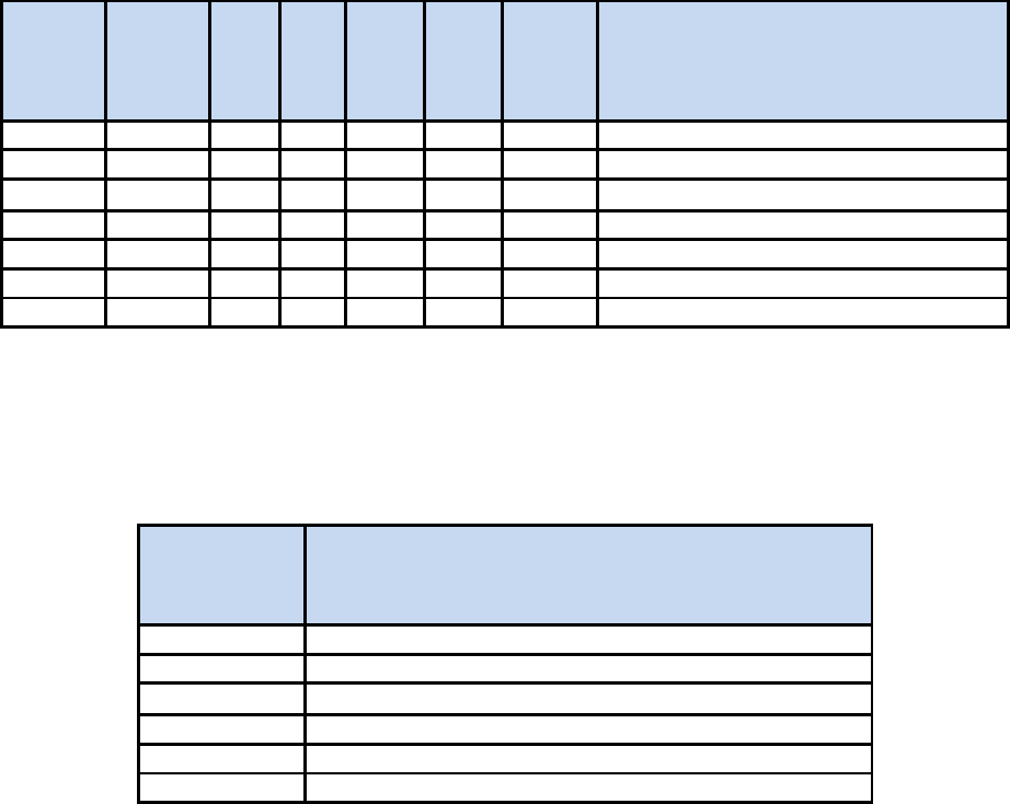
Consult Table 3 for the applicable power settings. The LN100 is a multi-modem system operating between 150-
174MHz, in channel bandwidths of 6.25kHz, 12.5kHz, and 25.0kHz. Modulation choices in each bandwidth include
CPFSK, QPSK, 16QAM, and 64QAM. OTA Rate and maximum power is based on the modem choice and the
applicable emission mask for the operating frequency.
Bandwidth
kHz
Modem
symbols
per
second
CPFSK
(x1)
OTA
bps
QPSK
(x2)
OTA
bps
16QAM
(x4)
OTA
bps
64QAM
(x6)
OTA
bps
Maximum
Output
Power
Comments / Restrictions
6.25
4800
--
9600
19200
28800
41.4 dBm
Max. Rate depends on operating frequency
12.5
9600
--
19200
38400
57600
41.4 dBm
Max. Rate depends on operating frequency
12.5
10000
--
20000
40000
60000
41.4 dBm
Max. Rate depends on operating frequency
12.5
9600
9600
--
--
--
41.4 dBm
Max. Rate depends on operating frequency
25.0
16000
--
32000
64000
96000
41.4 dBm
Max. Rate depends on operating frequency
25.0
20000
--
40000
80000
120000
41.4 dBm
Max. Rate depends on operating frequency
25.0
19200
19200
--
--
--
41.4 dBm
Max. Rate depends on operating frequency
Table 3. LN100 Power Output
5.3 Offered Antennas
Consult Table 4 for offered antennas.
Part#
Description
97-4278A20
Yagi 150-174MHz 7dBd
97-4278A21
Yagi 150-174MHz 9.2dBd
97-4278A22
Yagi 150-174MHz 10.2dBd
97-4278A26
Omni 150-156MHz 3dBi
97-4278A27
ANTENNA, OMNI, 156-162MHz, 3dBi
97-4278A28
FG,Omnidrct'l Ant,3 dBi gain,168-174 MHz
Table 4. LN100 offered antennas