Gainspan GS2011MIE Ultra-Low Power Wi-Fi Module User Manual
Gainspan Corporation Ultra-Low Power Wi-Fi Module
Gainspan >
Users Manual

Release 0.9, 03/18/2014
Copyright © 2014 GainSpan. All rights reserved.
Preliminary
Confidential
GS2011M Low Power WiFi Module
Data Sheet
GS2011M-DS-001211
GainSpan®
802.11b/g/n Ultra-Low Power WiFi®
Series Modules

FCC Communications
Commission (FCC)
Interference Statement
This equipment has been tested and found to comply with the limits for a Class B digital
device, pursuant to Part 15 of the FCC Rules. These limits are designed to provide
reasonable protection against harmful interference in a residential installation. This
equipment generates uses and can radiate frequency energy and, if not installed and used
in accordance with the instructions may cause harmful interference to radio communications.
However, there is no guarantee that interference will not occur in a particular installation. If
this equipment does cause harmful interference to radio or television reception, which can be
determined by turning the equipment off and on, the user is encouraged to try to correct the
interference by one of the following measures:
• Reorient or relocate the receiving antenna
• Increase the separation between the equipment and receiver
• Connect the equipment into an outlet on a circuit different from that to which
the receiver is connected
• Consult the dealer or an experienced radio/TV technician for help
FCC Caution: To assure continued compliance, (example - use only shielded interface
cables when connecting to computer or peripheral devices). Any changes or modifications
not expressly approved by the party responsible for compliance could void the user’s
authority to operate this equipment.
This device complies with Part 15 of the FCC Rules. Operation is subject to the following two
conditions: (1) This device may not cause harmful interference, and (2) this device must
accept any interference received, including interference that may cause undesired operation.
FCC & IC Radiation
Exposure Statement
This equipment complies with FCC & IC radiation exposure limits set forth for an uncontrolled
environment. This equipment should be installed and operated with minimum distance 20cm
between the radiator & your body.
This transmitter must not be co-located or operating in conjunction with any other antenna or
transmitter must not be co-located or operating in conjunction with any other antenna or
transmitter. This device intended only for OEM integrators under the following conditions:
1. The antenna must be installed such that 20cm is maintained between the antenna and
users, and
2. The transmitter module may not be co-located with any other transmitter or antenna. As
long as 2 conditions above are met, further transmitter test will not be required.
However, the OEM integrator is still responsible for testing their end-product for any
additional compliance requirements required with this module installed (for example,
digital device emissions, PC peripheral requirements, etc.).
3. digital device emissions, PC peripheral requirements, etc.).
4. digital device emissions, PC peripheral requirements, etc.).
IMPORTANT NOTE: In the event that these conditions cannot be met (for example certain
laptop configurations or co-location with another transmitter), then the FCC & IC
authorizations are no longer considered valid and the FCC & IC IDs cannot be used on the
final product. In these circumstances, the OEM integrator will be responsible for re-evaluating
the end product (including the transmitter) and obtaining separate FCC & IC authorizations.
End Product Labeling: This transmitter module is authorized only for use in device where
the antenna may be installed such that 20cm may be maintained between the antenna and
users (for example access points, routers, wireless ADSL modems, and similar equipment).
the final product must be labeled in a visible area with the corresponding FCC ID number.

IC Certification - Canada The labeling requirements for Industry Canada are similar to those of the FCC. A visible label
on the outside of the final product must display the IC labeling. The user is responsible for
the end product to comply with IC ICES-003 (Unintentional radiators).
English
This device complies with Industry Canada license-exempt RSS standard(s). Operation is
subject to the following two conditions:
1. This device may not cause harmful interference
2. This device must accept any interference received, including received, including
interference that may cause undesired operation of the device.
French
Cet appareil est conforme à Industrie Canada une licence standard RSS exonérés (s). Son
fonctionnement est soumis aux deux conditions suivantes:
1. Cet appareil ne doit pas provoquer d'interférences
2. Cet appareil doit accepter toute interférence reçue, y compris les interférences pouvant
provoquer un fonctionnement indésirable de l'appareil.
Manual Information That Must be Included
The user’s manual for end users must include the following information in a prominent
location.
IMPORTANT NOTE: To comply with FCC & IC RF exposure compliance requirements, the
antenna used for this transmitter must be installed to provide a separation distance of at least
20cm from all persons and must not be co-located or operating in conjunction with any other
antenna or transmitter.
Other Notes: GainSpan modules have been built or under development for near body
exposure applications. The 20cm statement is a standard note because absorption rate
testing (commonly knowns as SAR or Specific absorption rate) is not modularly transferable
for FCC/IC. Thus, if a radio is being used against the body, the end user is still responsible
to test for regulatory near body exposure testing (for USA, please refer to the following):
• FCC Part 1.1037
• FCC Part 2.1091 Mobile Devices
• FCC Part 2.1093 Portable Devices
• FCC Part 15.247 (b) (4)

Copyright Statement This GainSpan manual is owned by GainSpan or its licensors and protected by U.S. and
international copyright laws, conventions, and treaties. Your right to use this manual is
subject to limitations and restrictions imposed by applicable licenses and copyright laws.
Unauthorized reproduction, modification, distribution, display or other use of this manual may
result in criminal and civil penalties.
GainSpan assumes no liability whatsoever, and disclaims any express or implied warranty,
relating to sale and/or use of GainSpan products including liability or warranties relating to
fitness for a particular purpose, merchantability, or infringement of any patent, copyright or
other intellectual property right. GainSpan products are not authorized for use as critical
components in medical, lifesaving, or life-sustaining applications
GainSpan may make changes to specifications and product descriptions at any time, without
notice.
Trademark GainSpan is a registered trademark of GainSpan Corporation. All rights reserved. Other
names and brands may be claimed as the property of others.
Contact Information In an effort to improve the quality of this document, please notify GainSpan Technical
Assistance at 1.408.627.6500 in North America or +91 80 42526503 outside North America.
Web and Email Contact www.gainspan.com
info@gainspan.com

GS2011M-DS-001211, Release 0.9 Confidential Preliminary 5
Table of Contents
Chapter 1 About This Manual ............................................................................................... 7
Revision History ..............................................................................................................7
Audience ......................................................................................................................... 8
Standards ........................................................................................................................ 8
Documentation Conventions ........................................................................................... 8
Documentation .............................................................................................................. 11
Documentation Feedback ....................................................................................... 12
Contacting GainSpan Technical Support ...................................................................... 12
Returning Products to GainSpan .................................................................................. 13
Guidelines for Packing Components for Shipment .................................................. 13
Accessing the GainSpan Portal .................................................................................... 14
Ordering Information ..................................................................................................... 14
Chapter 2 GS2011M Overview .......................................................................................... 15
Product Overview .......................................................................................................... 15
GS2011M Module Product Features ............................................................................. 15
Chapter 3 GS2011M Architecture ...................................................................................... 19
Architecture Description ................................................................................................ 19
Wireless LAN and System Control Subsystem ............................................................. 21
Onboard Antenna / RF Port / Radio ........................................................................ 21
802.11 MAC ....................................................................................................... 21
802.11 PHY ........................................................................................................ 22
RF/Analog .......................................................................................................... 23
Network Services Subsystem .................................................................................. 23
APP CPU ............................................................................................................ 23
Crypto Engine ..................................................................................................... 23
Memory Subsystem ................................................................................................. 23
SRAM ................................................................................................................. 23
ROM ................................................................................................................... 24
OTP ROM ........................................................................................................... 24
Flash Interface .................................................................................................... 24
Clocks ...................................................................................................................... 24
Real Time Clock (RTC) Overview ........................................................................... 25
RTC Main Features ............................................................................................ 25
Real Time Clock Counter ................................................................................... 26
RTC I/O .............................................................................................................. 27
DC_DC_CNTL .................................................................................................... 27
GS2011M Peripherals ............................................................................................. 27
SDIO Interface .................................................................................................... 27
SPI Interface ....................................................................................................... 28
UART Interface ................................................................................................... 28
I2C Interface ....................................................................................................... 28
GPIO .................................................................................................................. 29
ADC .................................................................................................................... 29

GS2011M Low Power WiFi Module Data Sheet
6 Confidential Preliminary GS2011M-DS-001211, Release 0.9
PWM ................................................................................................................... 29
System States ......................................................................................................... 30
Power Supply .......................................................................................................... 33
Chapter 4 Pin-out and Signal Description .......................................................................... 37
GS2011Mxx Device Pin-out .......................................................................................... 37
GS2011Mxx Module Pins Description ..................................................................... 38
GS2011M Pin MUX Function .................................................................................. 42
GS2011M Program and Code Restore Options ...................................................... 44
Chapter 5 Electrical Characteristics ................................................................................... 45
Absolute Maximum Ratings .......................................................................................... 45
Operating Conditions .................................................................................................... 46
Internal 1.8V Regulator ................................................................................................. 46
I/O DC Specifications .................................................................................................... 47
I/O Digital Specifications (Tri-State) Pin Types 4mA, 12mA, and 16mA ................. 47
I/O Digital Specifications for VDDIO=3.0V to 3.6V ............................................. 47
I/O Digital Specifications for VDDIO=2.25V to 2.75V ......................................... 48
I/O Digital Specs for VDDIO=1.7V to 1.98V ....................................................... 49
RTC I/O Specifications ............................................................................................ 50
Power Consumption (Estimate) .................................................................................... 50
802.11 Radio Parameters (Estimate) ............................................................................ 51
ADC Parameters ........................................................................................................... 51
Chapter 6 Package and Layout Guidelines ........................................................................ 53
GS2011Mxx Recommended PCB Footprint and Dimensions ....................................... 53

GS2011M-DS-001211, Release 0.9 Confidential Preliminary 7
Chapter 1 About This Manual
This manual describes the GS2011M Low Power module hardware specification.
Refer to the following sections:
• Revision History, page 7
• Audience, page 8
• Standards, page 8
• Documentation Conventions, page 8
• Documentation, page 11
• Contacting GainSpan Technical Support, page 12
• Returning Products to GainSpan, page 13
• Accessing the GainSpan Portal, page 14
• Ordering Information, page 14
Revision History
This version of the GainSpan GS2011M Low Power WiFi Data Sheet contains the
following new information listed in Table 1, page 7.
Table 1 Revision History
Version Date Remarks
0.6 April 2013 Initial Release
0.7 January 2014
Updated Pinout and Signal description diagram
and table (see GS2011Mxx Device Pin-out,
page 37).
Updated SDIO interface clock frequency (see
GS2100M Module Product Features, page 15).
Updated Power Consumption Estimates and
802.11 Radio Parameter Estimates (see Power
Consumption (Estimate), page 50 and 802.11
Radio Parameters (Estimate), page 51).
0.8 February 2014
Added Notation to describe the GPIO37 when
using SPI interface.. See GS2011Mxx Module
Pins Description, page 38.
0.9 March 2014 Added Regulator Notations in About this
Manual.

About This Manual GS2011M Low Power WiFi Module Data Sheet
Audience
8 Confidential Preliminary GS2011M-DS-001211, Release 0.9
Audience
This manual is designed to help system designers build low power, cost effective, flexible
platforms to add WiFi connectivity for embedded device applications using the GainSpan
GS2011M based module.
Standards
The standards that are supported by the GainSpan GS module series are:
– IEEE 802.11 b/g/n
Documentation Conventions
This manual uses the following text and syntax conventions:
– Special text fonts represent particular commands, keywords, variables, or window
sessions
– Color text indicates cross-reference hyper links to supplemental information
– Command notation indicates commands, subcommands, or command elements
Table 2, page 8, describes the text conventions used in this manual for software procedures
that are explained using the AT command line interface.
Table 2 Document Text Conventions
Convention Type Description
command syntax
monospaced font
This monospaced font represents command strings entered on a
command line and sample source code.
AT XXXX
Proportional font
description
Gives specific details about a parameter.
<Data> DATA
UPPERCASE
Variable parameter
Indicates user input. Enter a value according to the descriptions that
follow. Each uppercased token expands into one or more other token.
lowercase
Keyword parameter
Indicates keywords. Enter values exactly as shown in the command
description.
[ ]
Square brackets
Enclose optional parameters. Choose none; or select one or more an
unlimited number of times each. Do not enter brackets as part of any
command.
[parm1|parm2|parm3]

GS2011M Low Power WiFi Module Data Sheet About This Manual
Documentation Conventions
GS2011M-DS-001211, Release 0.9 Confidential Preliminary 9
?
Question mark
Used with the square brackets to limit the immediately following token
to one occurrence.
<ESC>
Escape sequence
Each escape sequence <ESC> starts with the ASCII character 27 (0x1B).
This is equivalent to the Escape key.
<ESC>C
<CR>
Carriage return Each command is terminated by a carriage return.
<LF>
Line feed Each command is terminated by a line feed.
<CR> <LF>
Carriage return
Line feed
Each response is started with a carriage return and line feed with some
exceptions.
< >
Angle brackets
Enclose a numeric range, endpoints inclusive. Do not enter angle
brackets as part of any command.
<SSID>
=
Equal sign
Separates the variable from explanatory text. Is entered as part of the
command.
PROCESSID = <CID>
.
dot (period)
Allows the repetition of the element that immediately follows it multiple
times. Do not enter as part of the command.
.AA:NN can be expanded to 1:01 1:02 1:03.
A.B.C.D
IP address
IPv4-style address.
10.0.11.123
X:X::X:X
IPv6 IP address
IPv6-style address.
3ffe:506::1
Where the : : represents all 0x for those address components not
explicitly given.
LINE
End-to-line input token
Indicates user input of any string, including spaces. No other parameters
may be entered after input for this token.
string of words
WORD
Single token
Indicates user input of any contiguous string (excluding spaces).
singlewordnospaces
Table 2 Document Text Conventions (Continued)
Convention Type Description
About This Manual GS2011M Low Power WiFi Module Data Sheet
Documentation Conventions
10 Confidential Preliminary GS2011M-DS-001211, Release 0.9
Table 3, page 10, describes the symbol conventions used in this manual for notification and
important instructions.
Table 3 Symbol Conventions
Icon Type Description
Note
Provides helpful suggestions needed in understanding
a feature or references to material not available in the
manual.
Alert Alerts you of potential damage to a program, device,
or system or the loss of data or service.
Caution Cautions you about a situation that could result in
minor or moderate bodily injury if not avoided.
Warning Warns you of a potential situation that could result in
death or serious bodily injury if not avoided.
Electro-Static Discharge
(ESD)
Notifies you to take proper grounding precautions
before handling a product.

GS2011M Low Power WiFi Module Data Sheet About This Manual
Documentation
GS2011M-DS-001211, Release 0.9 Confidential Preliminary 11
Documentation
The GainSpan documentation suite listed in Table 4, page 11 includes the part number,
documentation name, and a description of the document. The documents are available from
the GainSpan Portal. Refer to Accessing the GainSpan Portal, page 14 for details.
Table 4 Documentation List
Part Number Document Title Description
GS2K-QS-001205 GainSpan GS2000 Based Module Kit
Quick Start Guide
Provides an easy to follow guide on
how to unpack and setup GainSpan
GS2000 based module kit for the
GS2011M and GS2100M modules.
GS2K-EVB-FP-UG-001206 GainSpan GS2000 Based Module
Programming User Guide
Provides users steps to program the
on-board Flash on the GainSpan
GS2000 based modules using DOS or
Graphical User Interface utility
provided by GainSpan. The user guide
uses the evaluation boards as a
reference example board.
GS-S2W-APP-PRG-RG-001208
GainSpan Serial-to-WiFi Adapter
Application Programmer Reference
Guide
Provides a complete listing of AT serial
commands, including configuration
examples for initiating, maintaining,
and evaluating GainSpan WiFi series
modules.
GS2K-EVB-HW-UG-001210
GainSpan GS2000 Based Module
Evaluation Board Hardware User
Guide.
Provides instructions on how to setup
and use the GS2000 based module
evaluation board along with component
description, jumper settings, board
specifications, and pinouts.
GS2011M-DS-001211 GainSpan GS2011M Low Power
WiFi Module Data Sheet
Provides information to help WiFi
system designers to build systems using
GainSpan GS2011M module and
develop wireless applications.
GS2100M-DS-001212 GainSpan GS2100M Low Power
WiFi Module Data Sheet
Provides information to help WiFi
system designers to build systems using
GainSpan GS2100M module and
develop wireless applications.
GS2011MxxS-DS-001214 GainSpan GS2011MxxS Low Power
WiFi Module Data Sheet
Provides information to help WiFi
system designers to build systems using
GainSpan GS2011MxxS module and
develop wireless applications.

About This Manual GS2011M Low Power WiFi Module Data Sheet
Contacting GainSpan Technical Support
12 Confidential Preliminary GS2011M-DS-001211, Release 0.9
Documentation Feedback
We encourage you to provide feedback, comments, and suggestions so that we can improve
the documentation. You can send your comments by logging into GainSpan Support Portal.
If you are using e-mail, be sure to include the following information with your comments:
– Document name
– URL or page number
– Hardware release version (if applicable)
– Software release version (if applicable)
Contacting GainSpan Technical Support
Use the information listed in Table 5, page 12, to contact the GainSpan Technical Support.
For more Technical Support information or assistance, perform the following steps:
1. Point your browser to http://www.gainspan.com.
2. Click Contact, and click Request Support.
3. Log in using your customer Email and Password.
4. Select the Location and click Contact.
5. Select Support Question tab.
6. Select Add New Question.
7. Enter your technical support question, product information, and a brief description.
The following information is displayed:
• Telephone number contact information by region
• Links to customer profile, dashboard, and account information
• Links to product technical documentation
• Links to PDFs of support policies
Table 5 GainSpan Technical Support Contact Information
North America 1 (408) 627-6500 - techsupport@gainspan.com
Outside North America
Europe: EUsupport@gainspan.com
China: Chinasupport@gainspan.com
Asia: Asiasupport@gainspan.com
Postal Address
GainSpan Corporation
3590 North First Street
Suite 300
San Jose, CA 95134 U.S.A.

GS2011M Low Power WiFi Module Data Sheet About This Manual
Returning Products to GainSpan
GS2011M-DS-001211, Release 0.9 Confidential Preliminary 13
Returning Products to GainSpan
If a problem cannot be resolved by GainSpan technical support, a Return Material
Authorization (RMA) is issued. This number is used to track the returned material at the
factory and to return repaired or new components to the customer as needed.
For more information about return and repair policies, see the customer support web page
at: https://www.gainspan.com/secure/login.
To return a hardware component:
1. Determine the part number and serial number of the component.
2. Obtain an RMA number from Sales/Distributor Representative.
3. Provide the following information in an e-mail or during the telephone call:
– Part number and serial number of component
– You name, organization name, telephone number, and fax number
– Description of the failure
4. The support representative validates your request and issues an RMA number for
return of the components.
5. Pack the component for shipment.
Guidelines for Packing Components for Shipment
To pack an ship individual components:
– When you return components, make sure they are adequately protected with
packing materials and packed so that the pieces are prevented from moving
around inside the carton.
– Use the original shipping materials if they are available.
– Place individual components in electrostatic bags.
– Write the RMA number on the exterior of the box to ensure proper tracking.
NOTE: Do not return any components to GainSpan Corporation unless you have
first obtained an RMA number. GainSpan reserves the right to refuse shipments
that do not have an RMA. Refused shipments will be returned to the customer by
collect freight.
CAUTION! Do not stack any of the components.
About This Manual GS2011M Low Power WiFi Module Data Sheet
Accessing the GainSpan Portal
14 Confidential Preliminary GS2011M-DS-001211, Release 0.9
Accessing the GainSpan Portal
To find the latest version of GainSpan documentation supporting the GainSpan product
release you are interested in, you can search the GainSpan Portal website by performing the
following steps:
1. Go to the GainSpan Support Portal website.
2. Log in using your customer Email and Password.
3. Click the Actions tab to buy, evaluate, or download GainSpan products.
4. Click on the Documents tab to search, download, and print GainSpan product
documentation.
5. Click the Software tab to search and download the latest software versions.
6. Click the Account History tab to view customer account history.
7. Click the Legal Documents tab to view GainSpan Non-Disclosure Agreement
(NDA).
8. Click Download on the Item Browser section to open or save the document.
Ordering Information
To order GainSpan’s GS2011Mxx low power module contact a GainSpan Sales/Distributor
Representative. Table 6, page 14 lists the GainSpan device information.
NOTE: You must first contact GainSpan to set up an account, and obtain a
customer user name and password before you can access the GainSpan Portal.
Table 6 GS2011Mxx Ordering Information
Device Description Ordering Number Revision
Low power module with on-board antenna GS2011MIZ
Low power module with external antenna GS2011MIE
NOTE: Modules ship with test code ONLY. Designers must first program the
modules with a released firmware version. Designers should bring out GPIO27
pin (option to pull this pin to VDDIO during reset or power-on) and UART0 or SPI0
pins to enable programming of firmware into the module. For details refer to the
Programming the GainSpan Modules document.

GS2011M-DS-001211, Release 0.9 Confidential Preliminary 15
Chapter 2 GS2011M Overview
This chapter describes the GainSpan® GS2011M low power module hardware specification
overview.
• Product Overview, page 15
• GS2011M Module Product Features, page 15
Product Overview
The GS2011M low power based module provides cost effective, low power, and flexible
platform to add WiFi connectivity for embedded devices for a variety of applications, such
as wireless sensors and thermostats. It uses GS2000 SoC, which combines ARM® Cortex
M3-based processors with a 802.11b/g/n Radio, MAC, security, and PHY functions, RTC
and SRAM, up to 4 MB FLASH, and on board and off module certified antenna options.
The module provides a WiFi and regulatory certified IEEE 802.11b/g/n radio with
concurrent network processing services for variety of applications, while leverage existing
802.11 wireless network infrastructures.
GS2011M Module Product Features
• Family of modules with different antenna and output power options:
• GS2011MIx 22.8mm (0.90in) x 32.5 mm (1.28in) x 3.63mm (0.143in) 48-pin
PCB Surface Mount Package. Two SKU’s are:
– GS2011MIZ (on-board antenna)
– GS2011MIE (external antenna)
• The two SKUs are pin to pin compatible, and the user has to account only for
power consumption, and on-board antenna keep out (if used) to accommodate
“one size fits all” for various end applications.
• Simple API for embedded markets covering a large range of applications
• Fully compliant with IEEE 802.11b/g/n and regulatory domains:
– 802.11n: 1x1 single stream, 20 MHz channels, 400/800ns GI, MCS0 – 7
– Data rates of 7.2, 14.4, 21.7, 28.9, 43.3, 57.8, 65.0, 72.2 Mbps
– 802.11g: OFDM modulation for data rates of 6, 9, 12, 18, 24, 36, 48 and 54
Mb/s
– 802.11b: CCK modulation rates of 5.5 and 11 Mbps; DSSS modulation for
data rate of 1 and 2 Mbps

GS2011M Overview GS2011M Low Power WiFi Module Data Sheet
GS2011M Module Product Features
16 Confidential Preliminary GS2011M-DS-001211, Release 0.9
• WiFi Solution:
– WiFi security (802.11i):
– WPA™ - Enterprise, Personal
– WPA2™ - Enterprise, Personal
– Vendor EAP Type(s):
– EAP-TTLS/MSCHAPv2, PEAPv0/EAP-MSCHAPv2,
PEAPv1/EAP-GTC, EAP-FAST, EAP-TLS
• Hardware-accelerated high-throughput AES and RC4 encryption/decryption
engines for WEP, WPA/WPA2 (AES-CCMP and TKIP).
• Additional dedicated encryption HW engine to support higher layer encryption
such as IPSEC (IPv4 and IPv6), SSL/TLS, HTTPs, PKI, digital certificates, RNG,
etc.
• Dual ARM Cortex M3 Processor Platform:
•1
st Cortex M3 processor (WLAN CPU) for WLAN software
– Implements 802.11 b/g/n WLAN protocol services
– 320 KB dedicated SRAM
– 512 KB dedicated ROM
•2
nd Cortex M3 processor (APP CPU) for networking software
– Implements networking protocol stacks and user application software
– 384 KB dedicated SRAM
– 512 KB dedicated ROM
• 64KB shared dual ported SRAM for inter-processor communications
• 320 KB assignable (under SW control) SRAM
• Support processor clock frequencies for both CPU of up to 120MHz
• Based on Advanced Microprocessor Bus Architecture (AMBA) system:
– AMBA Multilayer High-Speed Bus (AHB)
– AMBA Peripheral Bus (APB)
• On-module controller
– Manages read/write/program/erase operations to the 4 MB flash memory
device on the module
– Supports higher performance QUAD SPI protocol operations
– Active power management
• Interfaces:
• SDIO:

GS2011M Low Power WiFi Module Data Sheet GS2011M Overview
GS2011M Module Product Features
GS2011M-DS-001211, Release 0.9 Confidential Preliminary 17
– Compliant to SDIO v2.0 specification
– Interface clock frequency up to 40 MHz
– Data transfer modes: 4-bit, 1-bit SDIO, SPI
– Device mode only
• SPI:
– Two (2) general-purpose SPI interfaces (each configurable independently as
master or slave)
– The SPI pins are muxed with other functions such as GPIO
– Supports clock rates of up to 30 MHz (master mode) and up to 10 MHz (slave
mode)
– Protocols supported include: Motorola SPI, TI Synchronous Serial Protocol
(SSP) and National Semiconductor Microwire
– Supports SPI mode 0 thru 3 (software configurable)
• UART:
– Two (2) multi-purpose UART interfaces operating in full-duplex mode
– 16450/16550 compatible
– Optional support for flow control using RTS/CTS signaling for high data
transfer rates
– Standard baud rate from 9600 bps up to 921.6 kbps (additional support for
higher non-standard rates using baud rates up to 7.5 MHz
• GPIOs:
– Up to 27 configurable general purpose I/O
• Single 3.3V supply option
– I/O supply voltage 1.8 ~ 3.3V option
• Three (3) PWM output
•I
2C master/slave interface
• Two 12-bit ADC channels, sample rate from 10 kS/s to 2 MS/s
• Three (3) RTC I/O that can be configured as:
– Up to three alarm inputs to asynchronously awaken the chip.
– Support of up to two control outputs for power supply and sensors.
• Embedded RTC (Real Time Clock) can run directly from battery.
• Power supply monitoring capability.
NOTE: Tested with current test platform up to 33 MHz.

GS2011M Overview GS2011M Low Power WiFi Module Data Sheet
GS2011M Module Product Features
18 Confidential Preliminary GS2011M-DS-001211, Release 0.9
• Low-power mode operations
– Standby, Sleep, and Deep Sleep
• FCC/IC/ETSI/TELEC/WiFi Certification (TBD)

GS2011M-DS-001211, Release 0.9 Confidential Preliminary 19
Chapter 3 GS2011M Architecture
This chapter describes the GainSpan® GS2011M Low Power module architecture.
• Architecture Description, page 19
• Wireless LAN and System Control Subsystem, page 21
Architecture Description
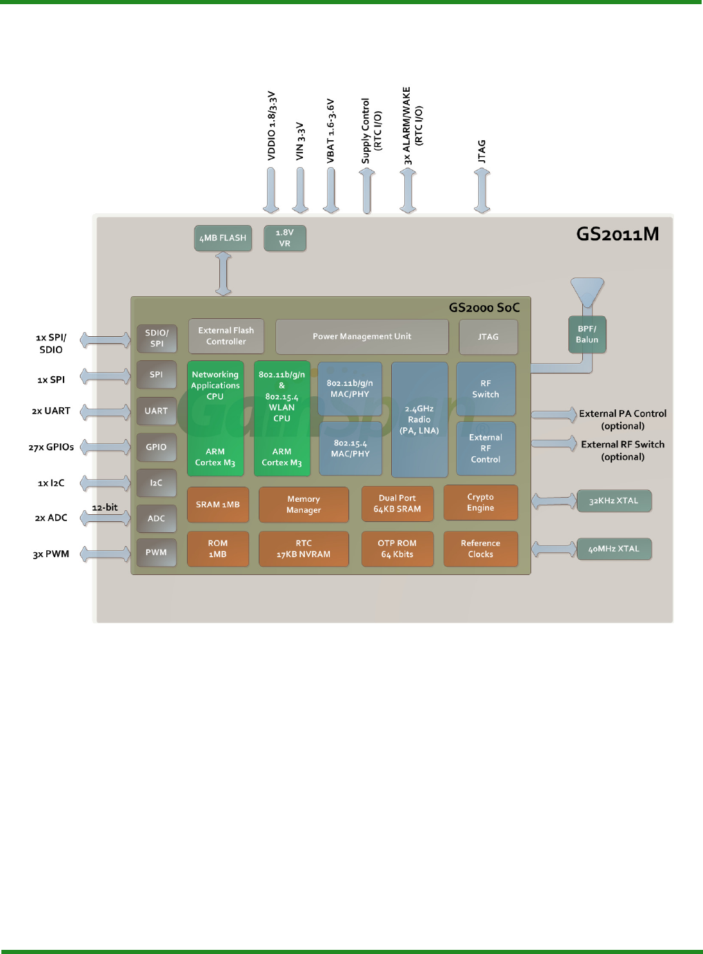
The GainSpan GS2011M module (see Figure 1, page 20) is based on a highly integrated
GS2000 ultra low power WiFi System-on-Chip (SoC) that contains the following:
• The GS2000 SoC contains two ARM Cortex M3 CPUs, a compatible 802.11
radio, security, on-chip memory, and variety of peripherals in a single package.
– One ARM core is dedicated to Networking Subsystems, and the other
dedicated to Wireless LAN Subsystems.
– The module carries an 802.11/g/n radio with on board 32KHz & 40 MHz
crystal circuitries, RF, and on-board antenna or external antenna options.
• On module 4 Mega Byte FLASH device that contains the user embedded
applications and data such as web pages.
• Variety of interfaces are available such as two UART blocks using only two data
lines per port with optional hardware flow controls, two SPI blocks (one SDIO is
shared function with one for the SPI interfaces), I2C with Master or slave
operation, JTAG port, low-power 12-bit ADC capable of running at up to 2M
samples/Sec., GPIO’s, and LED Drivers/GPIO with 16mA capabilities.
• GS2011Mxx has a VRTC pin that is generally connected to always available
power source such as battery or line power. This provides power to the Real Time
Clock (RTC) block on the SoC. The module contains a 1.8V regulator that is
turned on/off when going into the lowest power mode, i.e. standby mode. The
module also has VDDIO power supply input to provide the logic signal level for
the I/O pins. VDDIO must turn on/off with the 1.8V power.
GS2011M Architecture GS2011M Low Power WiFi Module Data Sheet
Architecture Description
20 Confidential Preliminary GS2011M-DS-001211, Release 0.9
Figure 1 GS2011M Block Diagram

GS2011M Low Power WiFi Module Data Sheet GS2011M Architecture
Wireless LAN and System Control Subsystem
GS2011M-DS-001211, Release 0.9 Confidential Preliminary 21
Wireless LAN and System Control Subsystem
The WLAN CPU subsystem consists of the WLAN CPU, its ROM, RAM, 802.11 b/g/n
MAC/PHY, and peripherals. This CPU is intended primarily to implement the 802.11 MAC
protocols. The CPU system has GPIO, Timer, and Watchdog for general use. A UART is
provided as a debug interface. A SPI interface is provided for specific application needs.
The WLAN CPU can access the RTC registers through an asynchronous AHB bridge.
WLAN CPU has only Flash read access to the on-board flash memory. The WLAN
subsystem interacts with the APP subsystem through a set of mailboxes and shared
dual–port memories.
The CPUs provide debug access through a JTAG/serial port. For GS2011 module, the
complete JTAG port is brought out for both CPUs. The CPUs also include code and data
trace and watch point logic to assist in-system debugging of SW.
The WLAN subsystem includes an integrated power amplifier, and provides management
capabilities for an optional external power amplifier. In addition, it contains hardware
support for AES-CCMP encryption (for WPA2) and RC4 encryption (for WEP & WPA
TKIP) encryption/decryption.
Onboard Antenna / RF Port / Radio
The GS2011Mxx modules have fully integrated RF frequency synthesizer, reference clock,
low power PA, and a high power PA (GS2011MIE) for extended range applications. Both
TX and RX chain in the module incorporate internal power control loops. The GS2011Mxx
modules also incorporate an on board antenna option plus a variety of regulatory certified
antenna options for various application needs.
802.11 MAC
The 802.11 MAC implements all time critical functionality of the 802.11b/g/n protocols. It
works in conjunction with the MAC SW running on the CPU to implement the complete
MAC functionality. It interfaces with the PHY to initiate transmit/receive and CCA. The
PHY registers are programmed indirectly through the MAC block. The MAC interfaces to
the system bus and uses DMA to fetch transmit packet data and save receive packet data.
The MAC SW exchanges packet data with the HW though packet descriptors and pointers.
Key Features
• Compliant to IEEE 802.11 (2012)
• Compliant to IEEE 802.11b/g/n (11n – 2009)
• Long and short preamble generation on frame-by-frame basis for 11b frames
• Transmit rate adaptation
• Transmit power control
• Frame aggregation (AMPDU, AMSDU)
• Block ACK (Immediate, Compressed)

GS2011M Architecture GS2011M Low Power WiFi Module Data Sheet
Wireless LAN and System Control Subsystem
22 Confidential Preliminary GS2011M-DS-001211, Release 0.9
• RTS/CTS, CTS-to-self frame sequences and SIFS
• Client and AP modes support
• Encryption support including: AES-CCMP, legacy WPA-TKIP, legacy WEP
ciphers and key management
• WiFi Protected Setup 2.0 (WPS2.0) including both PIN and push button options
• 802.11e based QoS (including WMM, WMM-PS)
• WiFi Direct with concurrent mode, including Device/Service Discovery, Group
Formation/Invitation, Client Power Save, WPS-PIN/Push Button
802.11 PHY
The 802.11 PHY implements all the standard required functionality and GainSpan specific
functionality for 802.11b/g/n protocols. It also implements the Radar detection
functionality to support 802.11h. The PHY implements the complete baseband Tx and Rx
pipeline. It interfaces with the MAC to perform transmit and receive operations. It
interfaces directly to the ADC and DAC. The PHY implements the Transmit power control,
receive Automatic Gain Control and other RF control signals to enable transmit and
receive. The PHY also computes the CCA for MAC use.
Key Features
• Compliant to 2.4GHz IEEE 802.11b/g/n (11n – 2009)
• Support 802.11g/n OFDM with BPSK, QPSK, 16-QAM and 64-QAM; 802.11b
with BPSK, QPSK and CCK
• Support for following data rates:
– 802.11n (20MHz): MCS0 - 7; 7.2, 14.4, 21.7, 28.9, 43.3, 57.8, 65.0, 72.2
Mbps
– 802.11g: 6, 9, 12, 18, 24, 36, 48, 54 Mbps
– 802.11b: 1, 2, 5.5, 11 Mbps
• Support Full (800ns) & Half (400ns) Guard Interval (GI) modes (SGI and LGI)
• Support Space time block coding (STBC) for receive direction
• Complete front-end radio integration including PA, LNA and RF Switch
• Support for external PA, LNA and control of external RF Switch (GS2011MIE
only)

GS2011M Low Power WiFi Module Data Sheet GS2011M Architecture
Wireless LAN and System Control Subsystem
GS2011M-DS-001211, Release 0.9 Confidential Preliminary 23
RF/Analog
The RF/Analog is a single RF transceiver for IEEE 802.11b/g/n (WLAN). The RF Interface
block provides the access to the RF and analog control and status to the CPU. This block is
accessible only from the WLAN CPU. It implements registers to write static control words.
It provides read only register interface to read static status. It generates the dynamic control
signals required for TX and RX based on the PHY signals. The AGC look up table to map
the gain to RF gain control word is implemented in this block.
Network Services Subsystem
APP CPU
The Network services subsystem consists of an APP CPU which is based on an ARM
CORTEX M3 core. It incorporates an AHB interface and a JTAG debug interface. The
network RTOS, network stack, and customer application code run on this CPU.
Crypto Engine
The Network services subsystem contains a separate hardware crypto engine that provides
a flexible framework for accelerating the cryptographic functions for packet processing
protocols. The crypto engine has the raw generic interface for cipher and hash/MAC
functions such as AES, DES, SHA, and RC4. It also includes two optional engines to
provide further offload; the PKA and RNG modules. These provide additional methods for
public key acceleration functions and random number generation. The engine includes a
DMA engine that allows the engine to perform cryptographic operation on data packets in
the system memory without any CPU intervention.
Memory Subsystem
The GS2011M module contains several memory blocks.
SRAM
The system memory is built with single port and dual port memories. Most of the memory
consists of single port memory. A 64KB dual port memory is used for exchange of data
between the two CPU domains. All the memories are connected to the system bus matrix
in each CPU subsystem. All masters can access any of the memory within the subsystem.
The APP subsystem has 384KB of dedicated SRAM for program and data use.
The WLAN subsystem has 320KB of dedicated SRAM for program and data use.
These memories are divided into banks of 64KB each. The bank structure allows different
masters to access different banks simultaneously through the bus matrix without incurring
any stall. Code from the external Flash is loaded into the SRAM for execution by each
CPU.
In addition, a static shared SRAM is provided. This consists of five 64KB memory blocks.

GS2011M Architecture GS2011M Low Power WiFi Module Data Sheet
Wireless LAN and System Control Subsystem
24 Confidential Preliminary GS2011M-DS-001211, Release 0.9
At any time, any of these memory blocks can be assigned to one of the CPU subsystem.
These should be set up by the APP CPU SW at initialization time. The assignment is not
intended to change during operation and there is no HW interlock to avoid switching in the
middle of a memory transaction. The assignment to the WLAN CPU should be done
starting from the highest block number going down to lowest block number. This result in
the shared memory appearing as a single bank for each CPU subsystem, independent of the
number of blocks assigned. The shared memory is mapped such that the SRAM space is
continuous from the dedicated SRAM to shared SRAM.
A 64KB dual port memory is used for exchange of data between the two CPU domains.
Each CPU subsystem can read or write to this memory using an independent memory port.
SW must manage the memory access to avoid simultaneous write to the same memory
location. The dual port memory appears as a single bank to each CPU subsystem.
ROM
ROM is provided in each CPU subsystem to provide the boot code and other functional
code that are not expected to change regularly. Each CPU has 512KB of ROM.
OTP ROM
The GS2000 device includes a 64Kbit OTP ROM used for storing MAC ID and other
information such as security keys etc. The APP and WLAN subsystem each contain
32Kbits (4Kbytes) of OTP memory.
Flash Interface
The GS2000 SoC has only internal ROM and RAM for code storage. There is no embedded
Flash memory on the SoC. Any ROM patch code and new application code must reside in
the on-module Flash device of the GS2011M module. Flash access from the two CPUs are
independent. The APP CPU is considered the system Master and the code running on this
CPU is required to initialize the overall chip and common interfaces. WLAN CPU access
to the Flash is restricted to read DMA. Any write to the Flash from the WLAN CPU must
be done through the APP CPU. The operational parameters of the DMA accesses are set by
the APP CPU at system startup. The Flash code is transferred to internal RAM before
execution.
Clocks
The GS2011M includes four basic clock sources:
– Low power 32KHz clock (see Real Time Clock (RTC) Overview, page 25)
– 40MHz Xtal Oscillator
– PLL to generate the internal 120MHz (CPU) and 80MHz (PHY) clocks from the
40MHz Xtal.
– High speed RC oscillator 80MHz

GS2011M Low Power WiFi Module Data Sheet GS2011M Architecture
Wireless LAN and System Control Subsystem
GS2011M-DS-001211, Release 0.9 Confidential Preliminary 25
Intermediate modes of operation, in which high speed clocks are active but some modules
are inactive, are obtained by gating the clock signal to different subsystems. The clock
control blocks within the device are responsible for generation, selection and gating of the
clocked used in the module to reduce power consumption in various power states.
Real Time Clock (RTC) Overview
To provide global time (and date) to the system, the GS2011Mxx module is equipped with
a low-power Real Time Clock (RTC). The RTC is the always on block that manages the
Standby state. This block is powered from a supply pin (VRTC) separate from the digital
core and may be powered directly from a battery. The RTC implementation supports a
voltage range of 1.6v to 3.6v.
RTC Main Features
• One 48-bit primary RTC counter as the primary reference for all timing events and
standby awake management
• 4 programmable IO pins with specific default behavior. These pins are in the RTC
IO domain.
– One (DC_DC_CNTL) is setup as output pin to control external regulator
– Three others (RTC_IO) which can be programmed to be either
– Maximum of two wakeup counters to generate periodic output (32-bit)
– Alarm inputs to wake up the GS2011M module from its sleep states
(deep-sleep/standby)
• Startup control counters with HW and SW override registers
• Power-on-reset control with brown-out detector
• RTC registers to hold RTC and wakeup control bits while the core domain is off
• 1Kbyte latch based memory (1.6-3.6v capable)
• 16KB of SRAM memory, divided into 4 equal blocks (1.2v capable)
• uLDO to supply the SRAM memory
• RTC logic is 1.6-3.6v capable
• 32 KHz RC oscillator
• 32768Hz crystal oscillator
• APB interface for CPU access
• Interrupts to CPU
An overview of RTC block diagram is shown in Figure 2, page 26. The RTC contains a
low-power 32.768KHz RC oscillator which provides fast startup at first application of
RTC power. It also supports an optional 32.768KHz crystal oscillator which can be
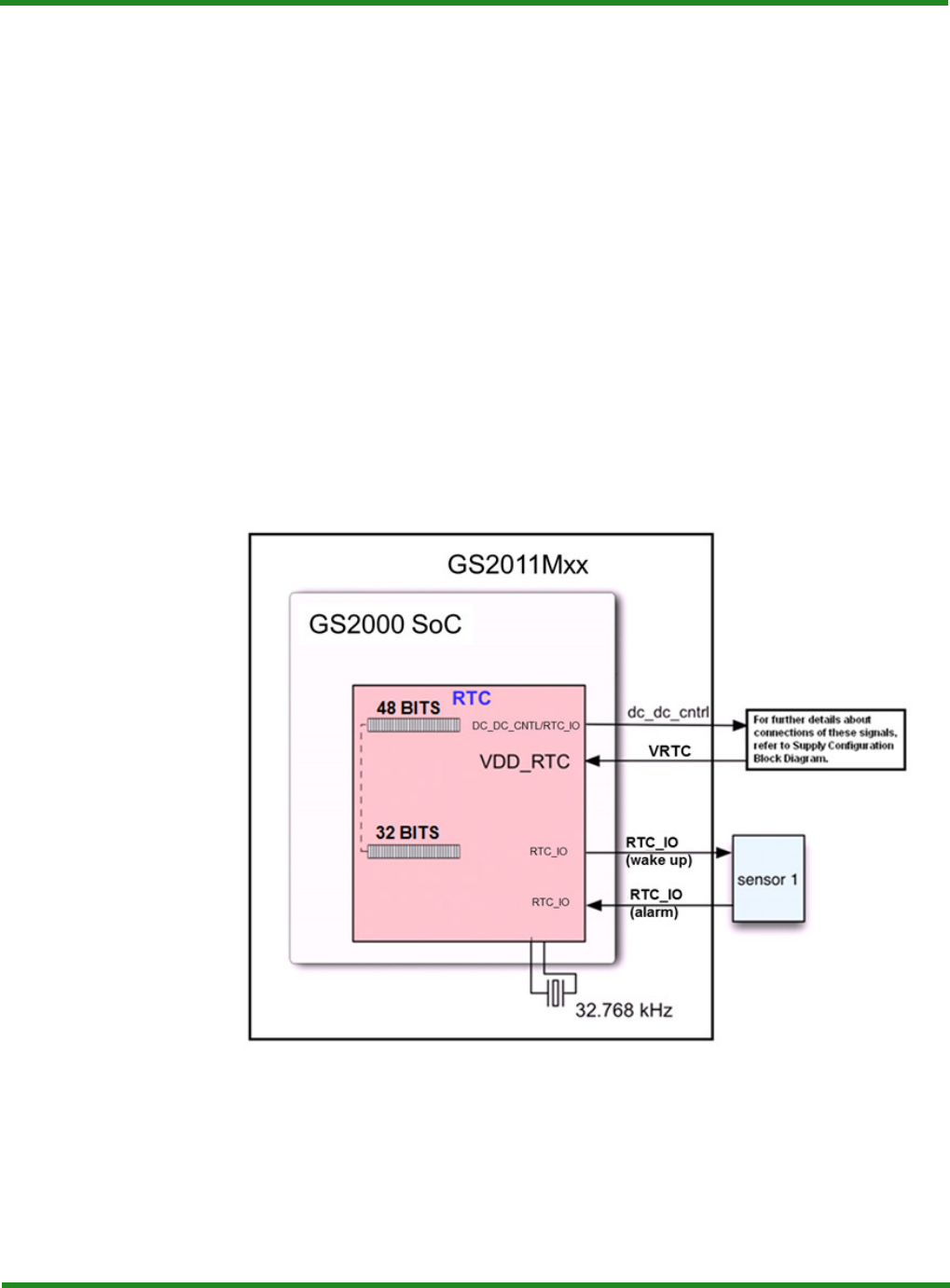
GS2011M Architecture GS2011M Low Power WiFi Module Data Sheet
Wireless LAN and System Control Subsystem
26 Confidential Preliminary GS2011M-DS-001211, Release 0.9
substituted for the RC oscillator under software control. In normal operation the RTC is
always powered up, even in the Power up state.
The dc_dc_cntl programmable counter is 48-bits and provides up to 272 years worth of
standby duration.
For the other RTC_IO pins, the programmable embedded counters (32-bit) are provided to
enable periodic wake-up of the remainder of the external system, and provide a 1.5 days
max period. The RTC_IO pins can be configured as inputs (ALARMS) or output (WAKE
UP) pins.
The RTC includes a Power-On Reset (POR) circuit, to eliminate the need for an external
component. The RTC contains low-leakage non-volatile (battery-powered) RAM, to enable
storage of data that needs to be preserved. It also includes a brown-out detector that can be
disabled by SW.
Total current consumption of the RTC is typically less than 5 μA with 1Kbyte of data
storage, using the 32.768 kHz oscillator.
Figure 2 RTC Interface Diagram
Real Time Clock Counter
The Real Time Counter features:
– 48-bit length (with absolute duration of 272 years).
– Low-power design.

GS2011M Low Power WiFi Module Data Sheet GS2011M Architecture
Wireless LAN and System Control Subsystem
GS2011M-DS-001211, Release 0.9 Confidential Preliminary 27
This counter is automatically reset by power-on-reset.
This counter wraps around (returns to “all-0” once it has reached the highest possible
“all-1” value).
RTC I/O
There are three (3) RTC I/O (0, 1,2) that can be used to control external devices, such as
sensors or wake up the module based on external events or devices.
DC_DC_CNTL
During RTC Power-on-Reset (e.g. when the battery is first connected), the dc_dc_cntl pin
is held low; it goes high to indicate completion of RTC power-on-reset. This pin can be
used as an enable into an external device such as voltage regulator. The dc_dc_cntl also is
held low when module is in standby and goes high to indicate wake up from standby.
GS2011M Peripherals
SDIO Interface
The SDIO interface is a full / high speed SDIO device controller. The Controller supports
SPI, 1-bit SD and 4-bit SD bus mode. The SDIO block has an AHB interface, which allows
the CPU to configure the operational registers residing inside the AHB Slave core. The CIS
and CSA area is located inside the internal memory of CPU subsystem. The SDIO Registers
(CCCR and FBR) are programmed by both the SD Host (through the SD Bus) and CPU
(through the AHB bus) via Operational registers. The SDIO block implements the AHB
master to initiate transfers to and from the system memory autonomously.
During the normal initialization and interrogation of the card by the SD Host, the card will
identify itself as an SDIO device. The SD Host software will obtain the card information in
a tuple (linked list) format and determine if that card’s I/O function(s) are acceptable to
activate. If the Card is acceptable, it will be allowed to power up fully and start the I/O
function(s) built into it.
The SDIO interface implements Function 1 in addition to the default Function 0. All
application data transfers are done through the Function 1.
The primary features of this interface are:
• Meets SDIO card specification version 2.0
• Conforms to AHB specification
• Host clock rate variable between 0 and 40 MHz
• All SD bus modes supported including SPI, 1 and 4 bit SD
NOTE: Tested with current test platform up to 33 MHz.

GS2011M Architecture GS2011M Low Power WiFi Module Data Sheet
Wireless LAN and System Control Subsystem
28 Confidential Preliminary GS2011M-DS-001211, Release 0.9
• Allows card to interrupt host in SPI, 1 and 4 bit SD modes
• Read and Writes using 4 parallel data lines
• Cyclic Redundancy Check CRC7 for command and CRC16 for data
integrity-CRC checking optional in SPI mode
• Programmable through a standard AHB Slave interface
• Writing of the I/O reset bit in CCCR register generates an active low reset output
synchronized to AHB Clock domain
• Card responds to Direct read/write (IO52) and Extended read/write (IO53)
transactions
• Supports Read wait Control operation
• Supports Suspend/Resume operation
SPI Interface
The SPI interface is a master slave interface that enables synchronous serial
communications with slave or master peripherals having one of the following: Motorola
SPI-compatible interface, TI synchronous serial interface or National Semiconductor
Microwire interface. In both master and slave configuration, the block performs
parallel-to-serial conversion on data written to an internal 16-bit wide, 8-deep transmit
FIFO and serial to parallel conversion on received data, buffering it in a similar 16-wide, 8
deep FIFO. It can generate interrupts to the CPU to request servicing transmit and receive
FIFOs and indicate FIFO status and overrun/underrun. The clock bit rate is SW
programmable. In master mode, the SPI block in GS2000 can perform up to 30 MHz and
in slave mode up to 10 MHz serial clock. The interface type, data size and interrupt masks
are programmable. It supports DMA working in conjunction with the uDMA engine.
UART Interface
The UART interface implements the standard UART protocol. It is 16450/16550
compatible. It has separate 32 deep transmit and receive FIFOs to reduce CPU interrupts.
The interface supports standard asynchronous communication protocol using start, stop and
parity bits. These are added and removed automatically by the interface logic. The data size,
parity and number of stop bits are programmable. It supports HW based flow control
through CTS/RTS signaling. A fractional baud rate generator allows accurate setting of the
communication baud rate. It supports DMA working in conjunction with the uDMA
engine.
I2C Interface
The I2C interface block implements the standard based two wire serial I2C protocol. The
interface can support both master and slave modes. It supports multiple masters, high speed
transfer (up to 3.4MHz), 7 or 10 bit slave addressing scheme, random and current address
transfer. It also supports clock stretching to interface with slower devices. It can generate
interrupts to the CPU to indicate specific events such as FIFO full/empty, block complete,
no ack error, and arbitration failure.

GS2011M Low Power WiFi Module Data Sheet GS2011M Architecture
Wireless LAN and System Control Subsystem
GS2011M-DS-001211, Release 0.9 Confidential Preliminary 29
GPIO
The GPIO block provides programmable inputs and outputs that can be controlled from the
CPU SW through an APB interface. Any number of inputs can be configured as an interrupt
source. The interrupts can be generated based on the level or the transition of a pin. At reset,
all GPIO lines defaults to inputs. Each pin can be configured as input or output from SW
control.
ADC
The ADC is a 12-bit, low-power, A-to-D converter capable of running at up to 2 Mbps.
The ADC is accessible from the APP CPU only. The ADC contains an internal band-gap
reference which provides a stable 1.4 V reference voltage. Alternatively, the ADC can be
programmed to use the VIN_3V3 external supply reference as the full-scale reference.
The ADC uses an input clock range of 10KHz to 2MHz. The input clock is generated by
an internal NCO (Number Controlled Oscillator). A conversion requires 1 clock cycles.
The ADC supports three measurement modes, continuous, single or periodic.
The sample data will be stored in a CPU readable FIFO. The file is an 8-deep FIFO. The
FIFO has SW configurable level interrupt. New samples are dropped if FIFO is full and
new data is received prior to FW servicing the FIFO, then the sample is dropped.
PWM
The PWM consists of three identical PWM function blocks. The PWM function blocks can
be used in two modes of operations:
• Independent PWM function blocks providing output signal with programmable
frequency and duty cycle
• Synchronized PWM function blocks with programmable phase delay between
each PWM output
The PWM has the following features:
• 32 bit AMBA APB interface to access control, and status information
• Three identical PWM function blocks
• Each PWM block can be enabled independently
• All three PWM blocks can be started synchronously or chained with
programmable delay
• Programmable 6 bit prescaler for the input clock (see Clocks, page 24)
• Programmable frequency and duty cycle using 16 bit resolution in terms of clock
cycles for ON and OFF interval time
• Combined interrupt line with independent masking of interrupts

GS2011M Architecture GS2011M Low Power WiFi Module Data Sheet
Wireless LAN and System Control Subsystem
30 Confidential Preliminary GS2011M-DS-001211, Release 0.9
System States
Figure 3, page 30 shows the power management/clock states of the GS2011Mxx system.
Figure 3 GS2011Mxx System States
The system states of the GS2011Mxx system are as follows:
Power OFF: No power source connected to the system.
Standby: In the standby state, only the RTC portion of the GS2011M is powered from
the VRTC pin. The other power supplies are turned off by the DC_DC_CNTL pin being
low. To achieve the lowest standby current, other supply pins should be powered on/off
together, controlled by the DC_DC_CNTL pin, including the EN_1V8 pin (which
controls VOUT_1V8), VDDIO, and the VIN_3V3 pin.

GS2011M Low Power WiFi Module Data Sheet GS2011M Architecture
Wireless LAN and System Control Subsystem
GS2011M-DS-001211, Release 0.9 Confidential Preliminary 31
In standby state, the 32.768KHz oscillator keeps running and only the RTC RAM
retains the state (how many banks retain their state is SW configurable). SRAM, CPUs
and I/Os are all in OFF state, as there is no 1.8V and no VDDIO being supplied to the
GS2011M device.
This is the lowest-power-consumption state. In a typical application, the system returns
to the Standby state between periods of activity, to keep the average power very low
and enable years of operation using conventional batteries. During standby, the RTC
isolates itself from the rest of the chip, since the signals from the rest of the chip are
invalid. This prevents corruption of the RTC registers.
Exit from standby occurs when a pre-specified wakeup time occurs, or when one of the
RTC_IO’s configured as alarm inputs sees the programmed polarity of signal edge.
When one of the wakeup conditions occurs, the RTC asserts reset to the chip and sets
the DC_DC_CNTL pin high to enable power to the rest of the module. After power to
the rest of the module is assumed to be good, the isolation between the RTC and the
rest of the chip is released, and the EXT_RESETn pin is released. The system now
starts booting.
System Configuration: When a power-up is requested, the system transitions from the
Standby state to the System Configuration state. In this state, the APP CPU is released
from reset by the RTC. The WLAN CPU remains in the reset state during System
Configuration. The APP CPU then executes the required system configurations,
releases the WLAN CPU from reset, and transitions to the Power-ON state.
The System Configuration state is also entered on transition from the Power-ON state
to the Standby state, to complete necessary preparations before shutting off the power
to the core system.
Power-ON: This is the active state where all system components can be running. The
Power-ON state has various sub-states, in which unused parts of the system can be in
sleep mode, reducing power consumption. Sleep states are implemented by gating the
clock signal off for a specific system component. Additionally, unneeded clock sources
can be turned off. For example, receiving data over a slave SPI interface could be done
with only the 80MHz RC oscillator active, and the 40MHz crystal and PLL turned off.
Sleep: In the Sleep state, the 40MHz crystal and the 80MHz RC oscillator remains
running, but it is gated off to one or both CPUs. Each CPU can independently control
its own entry into Sleep state. Any enabled interrupt will cause the interrupted CPU to
exit from Sleep state, and this will occur within a few clock cycles.
Deep Sleep: Deep sleep is entered only when both CPUs agree that the wakeup latency
is OK. In Deep Sleep mode, the 40MHz crystal oscillator and 80MHz RC oscillator are
turned off to save power, but all power supplies remain turned on. Thus all registers,
memory, and I/O pins retain their state. Any enabled interrupt will cause an exit from
Deep Sleep state.
NOTE: During first battery plug, i.e., when power is applied the first time to the
RTC power rail (VRTC), the power detection circuit in the RTC also causes a
wakeup request.

GS2011M Architecture GS2011M Low Power WiFi Module Data Sheet
Wireless LAN and System Control Subsystem
32 Confidential Preliminary GS2011M-DS-001211, Release 0.9
The following are not system states, but are related design notes:
Power Control: The GS2011M was designed with the intent that power to the
non-RTC portions of the chip be controlled from the DC_DC_CNTL signal. In
applications where it is preferred that an external host control the power, this is OK if
ALL power, including VRTC power, is turned on and off by the external host. In this
case, all state is lost when power goes off, and the latencies from first battery plug
apply.
If these latencies are not acceptable, then the GS2011M MUST control power. The
external host would use an alarm to wake it up, and a serial command to put it into
standby. The DC_DC_CNTL pin would control the power supplies. It is NOT reliable
for the external host to directly control the power supplies if VRTC is to be left turned
on. This is because the RTC would not know when to isolate itself from the rest of the
chip, and might get corrupted during power up or power down.
EXT_RESET_n pin: If the external host is driving the EXT_RESET_n pin, it MUST
do so with an open drain driver. This is because this pin is driven low during power up
by the RTC. In addition, if an external host is connected to the EXT_RESET_n pin,
there must be an external 10K ohm pull-up resistor on the board, pulling up to VDDIO.
This is needed to overcome a possible pull-down in the host at first power application.
It is also recommended that the host not actively assert EXT_RESET_n until all the
startup latencies have expired.
NOTE: For the above power states, software controls which clocks stay turned
on in each of the three states.
GS2011M Low Power WiFi Module Data Sheet GS2011M Architecture
Wireless LAN and System Control Subsystem
GS2011M-DS-001211, Release 0.9 Confidential Preliminary 33
Power Supply
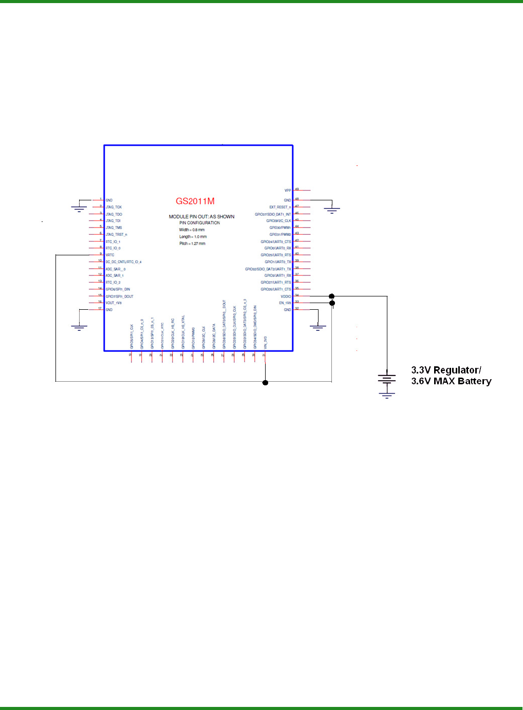
This section shows various application power supply connections. Figure 4, page 33 shows
the GS2011Mxx power supply connection and Figure 5, page 34 shows the GS2011Mxx in
battery powered with optimized active mode.
Figure 4 GS2011Mxx Always ON Power Supply Connection
Notes:
1. Always ON is obtained by trying EN_1V8 to 1 which is the enable for the
1.8V voltage regulator.
2. With this connection method, standby current will not be optimized.
GS2011M Architecture GS2011M Low Power WiFi Module Data Sheet
Wireless LAN and System Control Subsystem
34 Confidential Preliminary GS2011M-DS-001211, Release 0.9
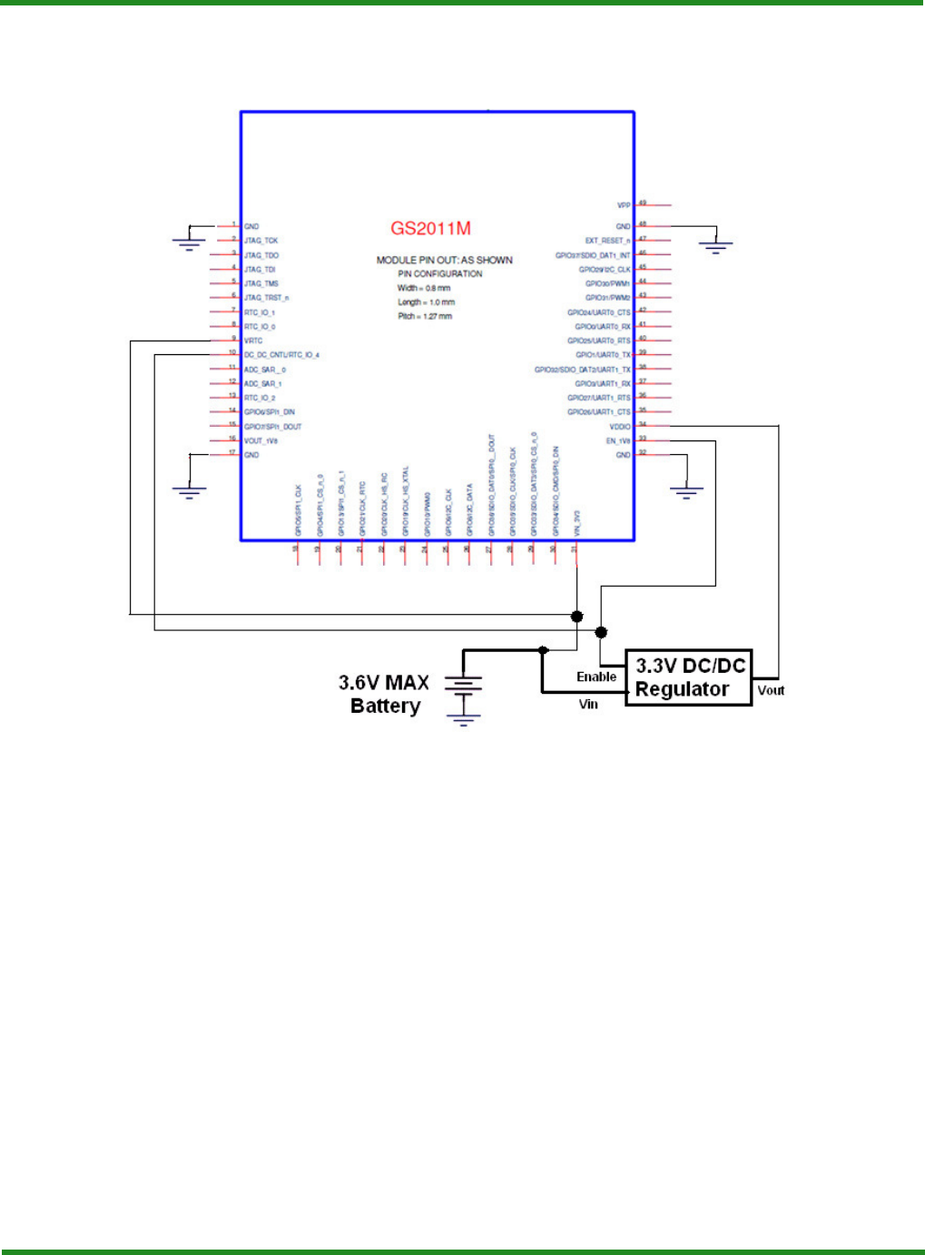
Figure 5 GS2011Mxx Battery Powered with Optimized Active Mode
Notes:
1. This connection applies for designs using GS2011MI module and want to
optimize active mode current consumption while still supporting standby state of
the module (see Figure 6, page 35). In this connection it is important to note the
following:
2. Input voltage to VRTC must always be ON to keep the RTC powered so that
the 32KHz crystal is running.
3. VDDIO power should be OFF during this state. Recommendation is to use
DC_DC_CNTL to also control the unit supplying the voltage to VDDIO
4. DC_DC_CNTL must be connected to EN_1V8 to so that the internal 1.8V
regulator gets turned OFF when system goes to standby state (i.e.
DC_DC_CNTL is de-asserted).
GS2011M Low Power WiFi Module Data Sheet GS2011M Architecture
Wireless LAN and System Control Subsystem
GS2011M-DS-001211, Release 0.9 Confidential Preliminary 35
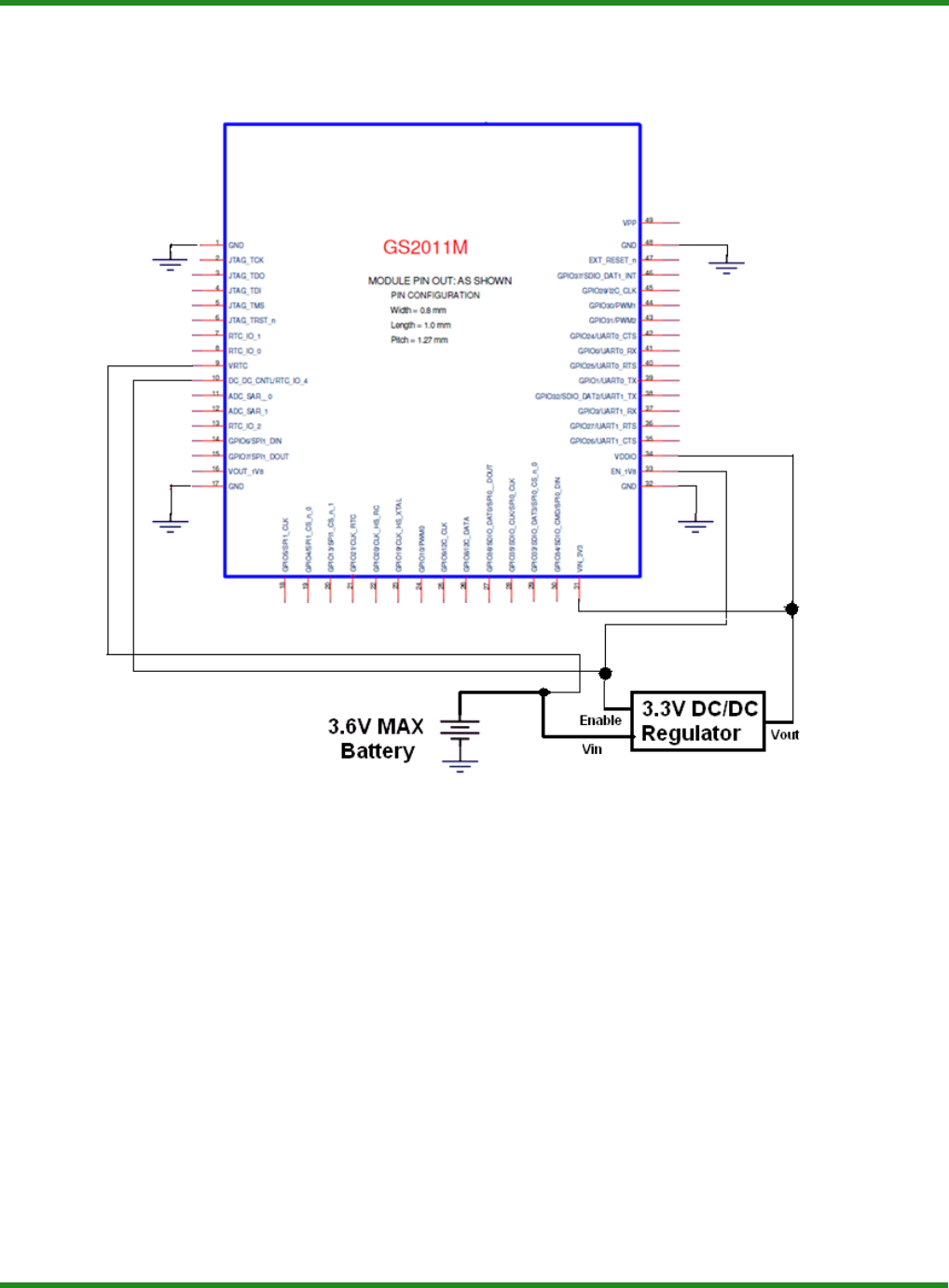
Figure 6 GS2011MIx Battery Powered with Optimized Standby Support
Notes:
1. This connection applies for designs (typically battery operated) using
GS2011MI module and want to optimized standby (lowest current consumption)
state of the module. In this connection it is important to note the following:
2. Input voltage to VRTC must always be ON to keep the RTC powered so that
the 32KHz crystal is running.
3. VDDIO and VIN_3V3power should be OFF during this state.
Recommendation is to use DC_DC_CNTL to also control the unit supplying the
voltage to VDDIO and VIN_3V3
4. DC_DC_CNTL must be connected to EN_1V8 to so that the internal 1.8V
regulator gets turned OFF when system goes to standby state (i.e.
DC_DC_CNTL is de-asserted).

GS2011M Architecture GS2011M Low Power WiFi Module Data Sheet
Wireless LAN and System Control Subsystem
36 Confidential Preliminary GS2011M-DS-001211, Release 0.9
- This page intentionally left blank -
GS2011M-DS-001211, Release 0.9 Confidential Preliminary 37
Chapter 4 Pin-out and Signal Description
This chapter describes the GainSpan® GS2011M Low Power module architecture.
• GS2011Mxx Device Pin-out, page 37
GS2011Mxx Device Pin-out
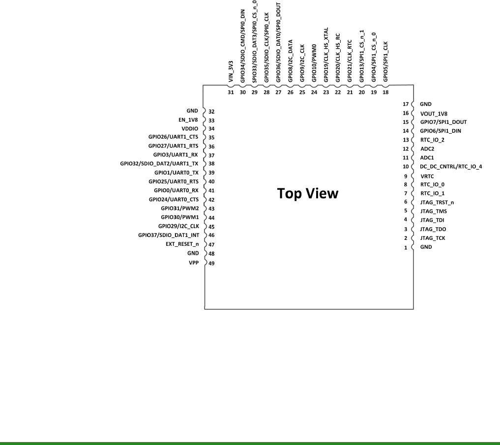
Figure 7, page 37 shows the GS2011Mxx device pin-out diagram.
Figure 7 GS2011Mxx Device Pin-out Diagram (Module Top View)

Pin-out and Signal Description GS2011M Low Power WiFi Module Data Sheet
GS2011Mxx Device Pin-out
38 Confidential Preliminary GS2011M-DS-001211, Release 0.9
GS2011Mxx Module Pins Description
Table 7, page 38 describes the GS2011Mxx module pin signal description.
Table 7 GS2011Mxx Module Pin Signal Description
Pins Name Voltage
Domain
Internal Bias after
Hardware Reset
Drive
Strength
(mA)
Signal State Description
1 GND 0V Not Applicable Analog port Ground
2 JTAG_TCK VDDIO Pull-up (see Note 1) Digital Input JTAG Test Clock
3 JTAG_TDO VDDIO Not Applicable Digital Output JTAG Test Data Out
4 JTAG_TDI VDDIO Pull-up (see Note 1) Digital Input JTAG Test Data In
5 JTAG_TMS VDDIO Pull-up (see Note 1) Digital Input JTAG Test Mode Select
6 JTAG_TRST_n VDDIO Pull-up (see Note 1) Digital Input JTAG Test Mode Reset
(Active Low)
7 RTC_IO_1 VRTC Pull-down (see Note 1)1 RTC Digital
Input/Output
Embedded Real Time Clock
Input/Output 1
8 RTC_IO_0 VRTC Pull-down (see Note 1)1 RTC Digital
Input/Output
Embedded Real Time Clock
Input/Output 0
9 VRTC VRTC Not Applicable Analog port Embedded Real Time Clock
Power Supply
10 DC_DC_CNTRL/
RTC_IO_4 VRTC (see Note 1) 1 RTC Digital
Input/Output
VIN_3V3 Regulator
Control Output/RTC Digital
Input/Output
11 ADC1 VIN_3V3 Not Applicable Analog Input General Analog to Digital
Converter 1
12 ADC2 VIN_3V3 Not Applicable Analog Input General Analog to Digital
Converter 2
13 RTC_IO_2 VRTC Pull-down (see Note 1)1 RTC Digital
Input/Output
Embedded Real Time Clock
Input/Output 2
14 GPIO6/SPI1_DIN VDDIO Pull-down 4 Digital
Input/Output
GPIO/Serial Peripheral
Interface 1 Bus Data Input
15 GPIO7 /
SPI1_DOUT VDDIO Pull-down 4 Digital
Input/Output
GPIO/Serial Peripheral
Interface 1 Bus Data Output
16 VOUT_1V8 VIN_3V3 Not Applicable Analog port Internal 1.8V VOUT
(internally regulated)
17 GND 0V Not Applicable Analog port Ground
18 GPIO5/SPI1_CLK VDDIO Pull-down 4 Digital
Input/Output
GPIO/Serial Peripheral
Interface 1 Bus Clock
19 GPIO4/
SPI1_CS_n_0 VDDIO Pull-down 4 Digital
Input/Output
GPIO/Serial Peripheral
Interface 1 Chip Select_0
(Active Low)

GS2011M Low Power WiFi Module Data Sheet Pin-out and Signal Description
GS2011Mxx Device Pin-out
GS2011M-DS-001211, Release 0.9 Confidential Preliminary 39
20 GPIO13/
SPI1_CS_n_1 VDDIO Pull-down 4 Digital
Input/Output
GPIO/ Serial Peripheral
Interface 1 Chip Select_1
(Active Low)
21 GPIO21/
CLK_RTC VDDIO Pull-down 4 Digital
Input/Output
GPIO/Internal RTC Clock
Circuitry Test Point. This
pin is used for Code
Restore.
22 GPIO20/
CLK_HS_RC VDDIO Pull-down 4 Digital
Input/Output
GPIO/Internal RTC Clock
Circuitry Test Point
23 GPIO19/
CLK_HS_XTAL VDDIO Pull-down 4 Digital
Input/Output
GPIO/XTAL Clock
Circuitry Test Point
24 GPIO10/PWM0 VDDIO Pull-down 4 Digital
Input/Output
GPIO/XTAL Clock
Circuitry Test Point
25 GPIO9/I2C_CLK VDDIO Pull-down (see Note 4) 12 Digital
Input/Output
GPIO/Inter-Integrated
Circuit Clock
26 GPIO8/I2C_DATA VDDIO Pull-down (see Note 4) 12 Digital
Input/Output
GPIO/Inter-Integrated
Circuit Data
27
GPIO36/
SDIO_DAT0/
SPI0_DOUT
VDDIO Pull-down (see Note 1)4 Digital
Input/Output
GPIO/SDIO Data Bit0/SPI0
Transmit Data Output to the
HOST
28
GPIO35/
SDIO_CLK/
SPI0_CLK
VDDIO Pull-down (see Note 1)4 Digital
Input/Output
GPIO/SDIO Clock/SPI0
Clock Input from the HOST
29
GPIO33/
SDIO_DAT3/
SPI0_CS_n_0
VDDIO Pull-up (see Note 1) 4 Digital Input
Output
GPIO/SDIO Data Bit
3/SPI0 Chip Select Input 0
from the HOST (Active
Low)
30
GPIO34/
SDIO_CMD/
SPI0_DIN
VDDIO Pull-down (see Note 1)4 Digital
Input/Output
GPIO/SDIO Command
Input/SPI0 Receive Data
Input from HOST
31 VIN_3V3 VIN_3V3 Not Applicable Analog port Single Supply Port
32 GND 0V Not Applicable Analog port Ground
33 EN_1V8 VDDIO Need to be driven
HIGH or LOW Digital Input Internal 1.8V regulator
enable port Active High
34 VDDIO VDDIO Not Applicable Analog port
All I/O voltage domain (can
be tied to VIN_3V3 or tied
to HOST I/O supply)
Table 7 GS2011Mxx Module Pin Signal Description (Continued)
Pins Name Voltage
Domain
Internal Bias after
Hardware Reset
Drive
Strength
(mA)
Signal State Description

Pin-out and Signal Description GS2011M Low Power WiFi Module Data Sheet
GS2011Mxx Device Pin-out
40 Confidential Preliminary GS2011M-DS-001211, Release 0.9
35 GPIO26/
UART1_CTS VDDIO Pull-down 4 Digital
Input/Output
GPIO/UART1Clear to Send
input (see Note 6)
36 GPIO27/
UART1_RTS VDDIO Pull-down (see Note 2) 4 Digital
Input/Output
GPIO/UART1 1 Request to
Send Output (see Note 6).
This pin is used for Program
Mode.
37 GPIO3/
UART1_RX VDDIO Pull-down 4 Digital
Input/Output
GPIO/UART1 Receive
Input
38
GPIO32/
SDIO_DAT2/
UART1_TX
VDDIO Pull-down 4 Digital
Input/Output
GPIO/SDIO_DATA Bit
2/UART 1 Transmitter
Output
39 GPIO1/
UART0_TX VDDIO Pull-down 4 Digital
Input/Output
GPIO/UART0 Transmitter
Output. This pin is used for
Code Restore.
40 GPIO25/
UART0_RTS VDDIO Pull-down 12 Digital
Input/Output
GPIO/UART0 Request to
Send Output (see Note 6).
This pin is used for Program
Select.
41 GPIO0/
UART0_RX VDDIO Pull-down 4 Digital
Input/Output
GPIO/UART0 Receive
Input
42 GPIO24/
UART0_CTS VDDIO Pull-down 12 Digital
Input/Output
GPIO/UART0 Clear to
Send Input (See Note 6)
43 GPIO31/PWM2 VDDIO Pull-down 16
(see Note 7)
Digital
Input/Output
GPIO/Pulse Width
Modulation Output 2
44 GPIO30/PWM1 VDDIO Pull-down 16
(see Note 7)
Digital
Input/Output
GPIO/Pulse Width
Modulation Output 1
45 GPIO29/I2C_CLK VDDIO Pull-down 12 Digital
Input/Output
GPIO/I2C_CLK (see Note
3)
46 GPIO37/
SDIO_DAT1_INT VDDIO Pull-down (see Note 9) 4 Digital
Input/Output
GPIO/4-bit SDIO DATA bit
1/SDIO SPI Mode Interrupt
47 EXT_RESET_n
(see Note 5) VDDIO
Digital Open
Drain
Input/Output
Module Hardware Reset
Input and Power Supply
Reset Monitor Indicator
Active Low
48 GND 0V Not Applicable Analog port Ground
49 VPP (see Note 8) VPP Analog port Programming Voltage for
OTP Memory
Table 7 GS2011Mxx Module Pin Signal Description (Continued)
Pins Name Voltage
Domain
Internal Bias after
Hardware Reset
Drive
Strength
(mA)
Signal State Description

GS2011M Low Power WiFi Module Data Sheet Pin-out and Signal Description
GS2011Mxx Device Pin-out
GS2011M-DS-001211, Release 0.9 Confidential Preliminary 41
Notes:
1. Pins with drive strength 4, 12, and 16 have one pull resistor (either up or down,
not both), which is enabled at reset. RTC_IO pins have both pull_up and
pull_down resisters. The RTC_IO pull down resisters are enabled at reset for non
DC_DC_CNTL pins.
2. This pin enables programming of the module. If UART1_RTS (GPIO27) is
high during reset or power on then the GS2011M will wait for Flash download
via UART0 or SPI0 interface. Route this pin on the base board so it can be pulled
up to VDDIO for programming the module.
3. GPIO29 is the primary function; if using GPIO8/9 as I2C function, then this
pin cannot be used for I2C function.
4. If I2C interface is used, provide 2K Ohm pull-ups, to VDDIO, for pins 25 and
26 (I2C_CLK and I2C_DATA).
5. EXT_RESET_n is an active low signal. It is an output during power up,
indicating to the system when GS2011 device is out of power-on-reset. After
power-on-reset, this pin is an input. It is not necessary to assert reset to the
GS2011M after power on, since the GS2011 has a built-in power on reset. Also,
the EXT_RESET_n signal does not clear the RTC, RTC RAM, or the SRAM. If
the external host is driving the EXT_RESET_n pin, it MUST do so with an open
drain driver. This is because this pin also must be able to be driven by the RTC.
In addition, if an external host is connected to the EXT_RESET_n pin, there
must be an external 10K Ohm pull-up resistor on the board, pulling up to
VDDIO.
6. CTS and RTS signals indicate it is clear to send or ready to send when they are
LOW. If signals are high indicates device is not ready.
7. These pins have higher drive strength so they can drive LEDs directly.
8. This pin is generally reserved for GainSpan use, but if a design requires
writing to OTP during production, then design must take into account connection
to this pin. Otherwise, it should be left as a No Connect.
9. In the Serial-to-WiFi firmware when using SPI interface this pin is the host
wake-up signal or the Ready to Send signal.
a. GPIO37 - when using SPI interface this pin is the host wake-up signal or
the Ready to Send signal.

Pin-out and Signal Description GS2011M Low Power WiFi Module Data Sheet
GS2011Mxx Device Pin-out
42 Confidential Preliminary GS2011M-DS-001211, Release 0.9
GS2011M Pin MUX Function
The GS2011M pins have multiple functions that can be selected using MUX function by
software. Each pin has an independent MUX select register. Table 8, page 42 shows the
various MUX functions for each pin. All pins are GPIO inputs at reset. For pins that are
inputs to functional blocks only one pin may be assigned to any input function. For
example, UART1_RX may be assigned to GPIO3 but not to both GPIO3 and GPIO37.
Table 8 GS2011M Pin MUX Description
Pin# Pin Name Mux3 Mux4 Mux5 Mux6 Mux7 Comments
1 GND
2 jtag_tck
3 jtag_tdo
4 jtag_tdi
5 jtag_tms
6 jtag_trst_n
7 rtc_io_1
8 rtc_io_0
9VRTC
10 dc_dc_cntl/rtc_io_4
11 adc_sar_0
12 adc_sar_1
13 rtc_io_2
14 gpio6/spi1_din spi1_din wspi_din spi1_dout wspi_dout spi0_cs_n_1
15 gpio7/spi1_dout spi1_dout wspi_dout spi1_din wspi_din spi0_cs_n_2
16 VOUT_1V8
17 GND
18 gpio5/spi1_clk spi1_clk wspi_clk pwm0 traceclk spi0_cs_n_3
19 gpio4/spi1_cs_n_0 spi1_cs_n_0 wspi_cs_n_0 spi0_cs_n_4 reserved clk_rtc
20 gpio13/spi1_cs_n_1 spi1_cs_n_1 pwm2 spi0_cs_n_5 tracedata[0] wspi_cs_n_1
21 gpio21/clk_rtc clk_rtc spi1_cs_n_2 clk_hs_xtal tracedata[1] spi0_cs_n_6
22 gpio20/clk_hs_rc clk_hs_rc spi1_cs_n_3 clk_hs_xtal tracedata[2] spi0_cs_n_7
23 gpio19_clk_hs_xtal clk_hs_xtal gpi1_cs_n_4 pwm2 tracedata[3] spi0_cs_n_8
24 gpio10/pwm0 pwm0 reserved reserved tracedata[0] clk_rtc
25 gpio9/i2c_clk i2c_clk uart1_rx reserved tracedata[1] i2s_lcrclk
26 gpio8/i2c_data i2c_data uart1_tx reserved tracedata[3] reserved
27 gpio36/sdio_dat0/spi0_dout sdio_data0 reserved i2c_data reserved spi0_dout
28 gpio35/sdio_clk/spi0_clk sdio_clk reserved i2c_clk traceclk spi0_clk Note: only
4mA for i2c
29 gpio33/sdio_dat3/spi0_cs_n_0 sdio_data3 reserved uart1_rts tracedata[0] spi0_cs_n_0
30 gpio34/sdio_cmd/spi0_din sdio_cmd reserved uart1_cts tracedata[1] spi0_din

GS2011M Low Power WiFi Module Data Sheet Pin-out and Signal Description
GS2011Mxx Device Pin-out
GS2011M-DS-001211, Release 0.9 Confidential Preliminary 43
31 VIN_3V3 Includes Flash,
PA, ADC,
VDDIO, REG
32 GND
33 EN_1V8
34 VDDIO
35 gpio26/uart1_cts uart1_cts wuart_cts i2s_din spi1_cs_n_13 wssp_clk
36 gpio27/uart1_rts uart1_rts wuart_rts i2s_dout uart1_tx wspi_dout
37 gpio3/uart1_rx uart1_rx wuart_rx i2s_bitclk spi1_cs_n_14 wsip_din
38 gpio32/sdio_dat2/uart1_tx sdio_data1 wuart_tx uart1_tx tracedata[2] spi1_cs_n_12
39 gpio1/uart0_tx uart0_tx wuart_tx pwm1 tracedata[0] spi1_dout
40 gpio25/uart0_rts uart0_rts wuart_rts reserved tracedata[1] spi1_clk
41 gpio24/uart0_cts uart0_rx wuart_rx pwm2 tracedata[2] spi1_din
42 gpio24/uart0_cts uart0_cts wuart_cts reserved tracedata[3] spi1_cs_n_0
43 gpio31/pwm2 pwm2 spi1_dout usart1_tx traceclk wuart_tx
44 gpio30/pwm1 pwm1 spi1_din uart1_rx reserved wuart_rx
45 gpio29/i2c_clk i2c_clk spi1_cs_n_20 clk_rtc tracedata[0] pwm0
46 gpio37/sdio_dat1_int sdio_data1 wuart_rx uart1_rx tracedata[3] spi0_cs_n_10
47 ext_reset_n
48 GND
49 VPP Programming
voltage for
OTP memory
Table 8 GS2011M Pin MUX Description (Continued)
Pin# Pin Name Mux3 Mux4 Mux5 Mux6 Mux7 Comments

Pin-out and Signal Description GS2011M Low Power WiFi Module Data Sheet
GS2011Mxx Device Pin-out
44 Confidential Preliminary GS2011M-DS-001211, Release 0.9
GS2011M Program and Code Restore Options
Table 9, page 44 describes the options available for device program mode and code restore
capabilities. The respective GPIO pins are sampled at reset by device and depending on the
values seen on these pins goes into the appropriate mode. Code for the GS2011M resides
on the internal flash of the module and up to two back-up copies could be stored in flash.
If a software designer wants to restore the execution code to one of the backup copy, it can
be accomplished by asserting the appropriate GPIO pins as shown in the table below during
power up or reset.
Table 9 GS2011M Pin Program and Code Restore
Program Mode
(GPIO 27)
Program Select
(GPIO 25)
Code Restore
(GPIO 21 or GPIO 1)
Description
0 X 0 Normal boot
0 0 1 Factory Code Restore
0 1 1 Previous Code Restore
10 X
Program Mode for code load using
UART 0 interface @115.2Kbaud or
using SPI0 on SDIO pins (Default Mode
if you don’t pull the Program Select pin
high)
11 X
Program Mode for code load using
UART 0 interface @921.6Kbaud or SPI0
interface on GPIO15-18 or using SDIO
interface.
Note: These options are targeted for a
future revision.

GS2011M-DS-001211, Release 0.9 Confidential Preliminary 45
Chapter 5 Electrical Characteristics
This chapter describes the GainSpan® GS2011M electrical characteristics.
• Absolute Maximum Ratings, page 45
• Operating Conditions, page 46
• Internal 1.8V Regulator, page 46
• I/O DC Specifications, page 47
• Power Consumption (Estimate), page 50
• 802.11 Radio Parameters (Estimate), page 51
• ADC Parameters, page 51
Absolute Maximum Ratings
Conditions beyond those cited in Table 10, page 45 may cause permanent damage to the
GS2011Mxx, and must be avoided. Sustained operation, beyond the normal operating
conditions, may affect the long term reliability of the module.
Note:
1. Reference domain voltage is the Voltage Domain. Refer to the section on
GS2011Mxx Module Pins Description. For limitations on state voltage ranges,
refer to the section GS2011Mxx Module Pins Description.
Table 10 Absolute Maximum Ratings
Parameter Symbol Minimum Typical Maximum Unit
Storage Temperature TST -55 +125 oC
RTC Power Supply VRTC -0.5 4.0 V
I/O Supply Voltage VDDIO -0.5 4.0 V
Single Supply Port VIN_3V3 0.5 3.3 4.0 V
OTP Supply VPP TBD V
Signal Pin Voltage1VI -0.3 Voltage Domain + 0.3 V
Electrical Characteristics GS2011M Low Power WiFi Module Data Sheet
Operating Conditions
46 Confidential Preliminary GS2011M-DS-001211, Release 0.9
Operating Conditions
Table 11, page 46 lists the operating conditions of the GS2011Mxx module.
Notes:
1. Reference domain voltage is the Voltage Domain. Refer to section
GS2011Mxx Module Pins Description.
2. The VPP pin should be left floating when not doing OTP programming
operations.
Internal 1.8V Regulator
Table 12, page 46 lists the internal 1.8V regulator parameters.
VIN_3V3=VDDIO=VRTC=3.3V Temp=25oC fOSC=3.0MHz.
Table 11 Operating Conditions
Parameter Symbol Minimum Typical Maximum Unit
Extended
Temperature Range TA-40 +85 oC
RTC Power Supply VRTC 1.6 3.3 3.6 V
I/O Supply Voltage VDDIO 1.7 3.3 3.6 V
Single Supply Port
GS2011MIx VIN_3V3 2.7 3.3 3.6 V
Signal Pin Voltage1VI 0 Voltage Domain V
VPP2VPP 5.5 5.75 6.0 V
Table 12 Internal 1.8V Regulator
Parameter Symbol Test
Conditions
Minimum Typical Maximum Unit
Output Voltage VOUT_1V8 1.8 V
Maximum Output Current IVOUT_1V8 30 50 mA
Oscillation Frequency fOSC 1.6 3.45 MHz
1.8V Regulator Enable “H:
Voltage EN_1V8 1.0 VIN_3V3 V
1.8V Regulator Enable “L”
Voltage EN_1V8 0 0.25 V

GS2011M Low Power WiFi Module Data Sheet Electrical Characteristics
I/O DC Specifications
GS2011M-DS-001211, Release 0.9 Confidential Preliminary 47
I/O DC Specifications
I/O Digital Specifications (Tri-State) Pin Types 4mA, 12mA, and 16mA
The specifications for these I/O’s are given over 3 different voltage ranges: 3.0V to 3.6V,
2.25V to 2.75V, and 1.7V to 1.98V.
I/O Digital Specifications for VDDIO=3.0V to 3.6V
Table 13, page 47 lists the parameters for I/O digital specification for VDDIO 3.0V to 3.6V
for Pin Types 4mA, 12mA, and 16mA.
Table 13 I/O Digital Parameters for VDDIO=3.0V to 3.6V
Parameter Symbol Minimum Typical Maximum Unit Note
I/O Supply Voltage VDDIO 3.0 3.3 3.6 V
Input Low Voltage VIL -0.3 0.8 V
Input High Voltage VIH 2.0 VDDIO V
Schmitt trigger Low to
High threshold point VT+ 1.62 1.75 1.91 V
Schmitt trigger High to
Low threshold point VT- 1.16 1.29 1.45 V
Input Leakage Current IL10 μAPull up/down
disabled
Tri-State Output
Leakage Current IOZ 10 μAPull up/down
disabled
Pull-Up Resistor Ru34K 51K 81K Ω
Pull-Down Resistor Rd35K 51K 88K Ω
Output Low Voltage VOL 0.4 V
Output High Voltage VOH 2.4 V
Low Level Output
Current @ VOL max IOL
4.9
15.1
20.2
7.5
22.9
30.6
10.0
30.4
40.6
mA
Pin Type 4mA
Pint Type 12mA
Pint Type 16mA
High Level Output
Current @ VOH min IOH
7.0
20.9
27.8
14.0
42.0
56.0
24.2
72.3
96.3
mA
Pin Type 4mA
Pin Type 12mA
Pin Type 16mA
Output rise time 10%
to 90% load, 30pF tTRLH
3.18
1.83
1.52
4.26
2.43
2.01
6.00
3.51
2.92
ns
Pin Type 4mA
Pint Type 12mA
Pin Type 16mA
Output fall time 90% to
10% load, 30pF tTFHL
3.88
1.88
1.56
4.99
2.51
2.10
7.16
3.63
3.05
ns
Pin Type 4mA
Pin Type 12mA
Pin Type 16mA

Electrical Characteristics GS2011M Low Power WiFi Module Data Sheet
I/O DC Specifications
48 Confidential Preliminary GS2011M-DS-001211, Release 0.9
I/O Digital Specifications for VDDIO=2.25V to 2.75V
Table 14, page 48 lists the parameters for I/O digital specification for VDDIO 2.25V to
2.75V for Pin Types 4mA, 12mA, and 16mA.
NOTE: The table below is an estimate. It is provided to give a rough idea of the
behavior at intermediate VDDIO voltages.
Table 14 I/O Digital Parameters for VDDIO = 2.25V to 2.75V
Parameter Symbol Minimum Typical Maximum Unit Note
I/O Supply Voltage VDDIO 2.25 2.5 32.75 V
Input Low Voltage VIL -0.3 0.7 V
Input High Voltage VIH 1.7 3.6 V
Schmitt trigger Low
to High threshold
point
VT+ 1.27 1.40 1.50 V
Schmitt trigger High
to Low threshold
point
VT- 0.85 0.98 1.10 V
Input Leakage
Current IL10 μAPull up/down
disabled
Tri-State Output
Leakage Current IOZ 10 μAPull up/down
disabled
Pull-Up Resistor Ru43K 69K 120K Ω
Pull-Down Resistor Rd41K 66K 124K Ω
Output Low Voltage VOL 0.7 V
Output High Voltage VOH 1.7 V
Low Level Output
Current @ VOL max IOL
5.7
17.4
23.3
9.6
29.2
39.1
14.1
42.8
57.2
mA
Pin Type 4mA
Pin Type 12mA
Pin Type 16mA
High Level Output
Current @ VOH min IOH
4.7
14.0
18.6
9.7
29.0
38.7
17.4
51.9
69.2
mA
Pin Type 4mA
Pin Type 12mA
Pin Type 16mA
Output rise time 10%
to 90% load, 30pF tTRLH
3.82
2.05
1.70
5.52
2.93
2.42
8.45
4.61
3.83
ns
Pin Type 4mA
Pin Type 12mA
Pin Type 16mA
Output fall time 90%
to 10% load, 30pF tTFHL
4.19
2.11
1.77
5.82
3.01
2.53
9.13
4.72
3.97
ns
Pin Type 4mA
Pin Type 12mA
Pin Type 16mA

GS2011M Low Power WiFi Module Data Sheet Electrical Characteristics
I/O DC Specifications
GS2011M-DS-001211, Release 0.9 Confidential Preliminary 49
I/O Digital Specs for VDDIO=1.7V to 1.98V
Table 15, page 49 lists the parameters for I/O digital specification for VDDIO 1.7V to
1.98V for Pin Types 4mA, 12mA, and 16mA.
Note:
1. These values do not meet the requirements of JEDEC JESD8-7A.
Table 15 I/O Digital Parameters for VDDIO = 1.7V to 1.98V
Parameter Symbol Minimum Typical Maximum Unit Note
I/O Supply Voltage VDDIO 1.7 1.8 1.98 V
Input Low Voltage VIL -0.3 0.631V
Input High Voltage VIH 1.17 3.6 V
Schmitt trigger Low to
High threshold point VT+ 0.95 1.06 1.16 V
Schmitt trigger High to
Low threshold point VT- 0.5810.69 0.79 V
Input Leakage Current IL10 μAPull up/down
disabled
Tri-State Output
Leakage Current IOZ 10 μAPull up/down
disabled
Pull-Up Resistor Ru66K 114K 211K Ω
Pull-Down Resistor Rd58K 103K 204K Ω
Output Low Voltage VOL 0 0.45 V
Output High Voltage VOH 1.35 V
Low Level Output
Current @ VOL max IOL
2.6
8.0
10.8
4.8
14.7
19.7
7.8
23.8
31.8
mA
Pin Type 4mA
Pin Type 12mA
Pin Type 16mA
High Level Output
Current @ VOH min IOH
1.7
5.0
6.6
4.1
12.4
16.5
8.3
24.9
33.2
mA
Pin Type 4mA
Pin Type 12mA
Pin Type 16mA
Output rise time 10%
to 90% load, 30pF tTRLH
5.37
2.67
2.19
8.42
4.16
3.42
13.86
6.99
5.76
ns
Pin Type 4mA
Pin Type 12mA
Pin Type 16mA
Output fall time 90%
to 10% load, 30pF tTFHL
5.29
2.73
2.30
8.15
4.24
3.57
13.98
7.17
6.06
ns
Pin Type 4mA
Pin Type 12mA
Pin Type 16mA
Electrical Characteristics GS2011M Low Power WiFi Module Data Sheet
Power Consumption (Estimate)
50 Confidential Preliminary GS2011M-DS-001211, Release 0.9
RTC I/O Specifications
Table 16, page 50 lists the RTC I/O parameters.
*RTC I/O’s are software selectable as 1mA or 4mA drive strength.
Power Consumption (Estimate)
Table 17, page 50 lists the power consumption estimates for the GS2011Mxx. Typical
conditions are: VIN_3V3=VDDIO=VRTC=3.3V Temp=25oC.
Note:
1. To be optimized and updated with production version.
Table 16 RTC I/O Parameters
Parameter Symbol Minimum Typical Maximum Unit Note
Supply Voltage 1.6 3.6 V
Input Low
Voltage VIL 0.3*VDD V
Input High
Voltage VIH 0l7*VDD V
Input Leakage
Current IL0.1 μA
Pullup Current IPU 1μA
Pulldown
Current IPU 1μA
Output Low
Voltage VOL 0.4 V IL=1mA or
4mA*
Output High
Voltage VOHJ VDD-0.4 V IL=1mA or
4mA*
Table 17 Power Consumption in Different States
System State Current (Typical)1
Standby (VIN_3V3 and VDDIO OFF) 4-8 μA
Deep Sleep (2 banks of SRAM enabled) 200 μA
WLAN Continuous Transmit (1 Mbps, 15 dBm) 200 mA
WLAN Continuous Receive (1 Mbps, -93 dBm sensitivity) 75 mA
IEEE 802.11 PS-Poll, DTIM = 1 (only WLAN enabled) TBD
IEEE 802.11 PS-Poll, DTIM=3 (only WLAN enabled) TBD

GS2011M Low Power WiFi Module Data Sheet Electrical Characteristics
802.11 Radio Parameters (Estimate)
GS2011M-DS-001211, Release 0.9 Confidential Preliminary 51
802.11 Radio Parameters (Estimate)
Table 18, page 51 lists the 802.11 Radio parameters (estimate). Test conditions are:
VIN_3V3=VDDIO=VRTC=3.3V Temp=25oC.
ADC Parameters
Table 19, page 51 lists the ADC parameters. Test conditions are:
VIN_3V3=VDDIO=VRTC=3.3V Temp=25oC.
Table 18 802.11 Radio Parameters
Parameter Minimum Typical Maximum Unit Notes
RF Frequency Range 2412 2497 MHz
Radio bit rate 1 HT20
MCS7 Mbps
Transmit/Receive Specification for GS2011M
Output power
(average)
15
12
8
dBm
11b, 1Mbps, BPSK/DSSS
11n, MCS 0 (6.5 Mbps), BPSK/OFDM
11n, MCS 7 (72 Mbps),
64-QAM/OFDM
Spectrum Mask dBr Meets 802.11 requirement for selected
data rates
Receive Sensitivity at
antenna port
-93
-74
-71
dBm
11b, 1, Mbps, BPSK/DSSS
11g, 54 Mbps, 64-QAM/OFDM
11n, MCS 7 (72 Mbps),
64-QAM/OFDM
Table 19 ADC Parameters
Parameter Minimum Typical Maximum Unit Notes
ADC Resolution - 12 - Bits
Conversion Speed (FS) 0.01 - 2 Msps
Input Voltage Full Scale
range
0 1.4 V Internal
Reference
0 VIN_3V3 V External
Reference
ADC Integral
Non-Linearity (INL) --
+2 LSB
ADC Differential
non-linearity (DNL) --
+1 LSB See Note 1

Electrical Characteristics GS2011M Low Power WiFi Module Data Sheet
ADC Parameters
52 Confidential Preliminary GS2011M-DS-001211, Release 0.9
Notes:
1. No missing codes.
2. This is the gain of the ADC core measured in External reference mode.
Active Current
800 μA
FS=2Mbps,
internal
reference
(Reference
Buffer on) 3.3V
550 μA
FS=32KHz,
internal
reference
(Reference
Buffer on) 3.3V
450 μA
FS=2Mbps,
External
reference
(Reference
Buffer off) 3.3V
180 μA
FS=32KHz,
internal
reference
(Reference
Buffer off) 3.3V
ADC Offset Error -30 - 30 mV
ADC Gain Error -8 - 8 LSB See Note 2
Error in Internal
Reference Voltage
without Trim
-5 - 5 %
Error in Internal
Reference Voltage with
Trim
-2.5 2.5 %
Table 19 ADC Parameters (Continued)
Parameter Minimum Typical Maximum Unit Notes
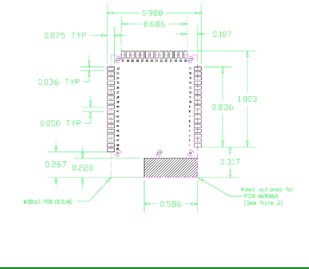
GS2011M-DS-001211, Release 0.9 Confidential Preliminary 53
Chapter 6 Package and Layout Guidelines
This chapter describes the GainSpan® GS2011M package and layout guidelines.
• GS2011Mxx Recommended PCB Footprint and Dimensions, page 53
GS2011Mxx Recommended PCB Footprint and Dimensions
Figure 8, page 53 shows the GS2011MIx Module PCB Footprint. Figure 9, page 54 shows
the GS2011MIx Module Dimensions.
Figure 8 GS2011MIx Module Recommended PCB Footprint (in inches)
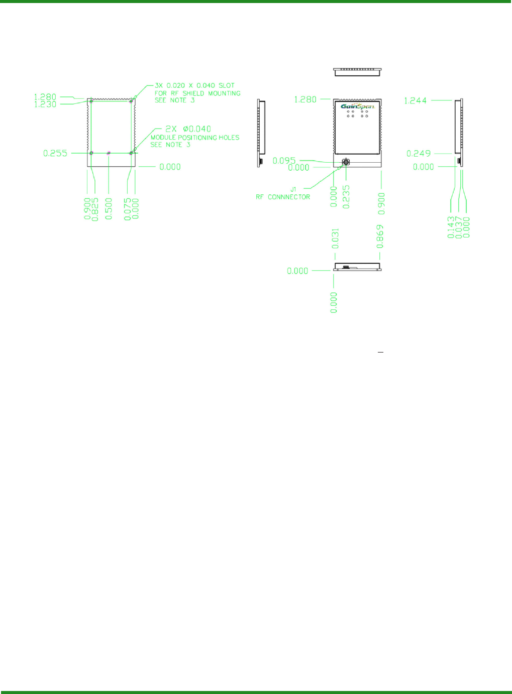
Package and Layout Guidelines GS2011M Low Power WiFi Module Data Sheet
GS2011Mxx Recommended PCB Footprint and Dimensions
54 Confidential Preliminary GS2011M-DS-001211, Release 0.9
Figure 9 GS2011MIx Module Dimensions (in inches)
Notes:
1. All Dimensions are in inches. Tolerances shall be + 0.010 inches.
2. Absolutely no metal trace or ground layer underneath this area. If using PCB
antenna, it is recommended to have only air under this area. Hang antenna over
edge of base board or cut notch in base board.
3. It is recommended not to run circuit traces underneath the module especially
near these holes. The RF shield mounting holes are grounded. If traces must be
routed under the GS2011Mxx, it is recommended that extra thick solder mask (5
mils) be used to prevent shorting. High speed signals should be kept as far as
possible from the antenna and RF areas of the GS2011Mxx.
4. In performing SMT or manual soldering of the module to the base board, first
align the row of pins from #18 through #31 onto the base board and then match
the other two rows.
In additional to the guidelines, note the following suggestions:
1. External Bypass capacitors for all module supplies should be as close as
possible to the module pins.
2. Never place the antenna very close to metallic objects.
3. External monopole antennas need a reasonable ground plane area for antenna
efficiency.
4. Do not use a metallic or metalized plastic for the end product enclosure when
using on-board antenna.
5. If the module is enclosed in a plastic case, have reasonable clearance from
plastic case to on-board antenna.