Gainspan GS2011MIZ Ultra-Low Power Wi-Fi Module User Manual
Gainspan Corporation Ultra-Low Power Wi-Fi Module
UserManual.wiki
>
Gainspan
>
GS2011MIZ User Manual
Users Manual
Navigation menu
Upload a User Manual
Namespaces
Wiki Guide
HTML
PDF
Info
Views
User Manual
Discussion / Help
Navigation

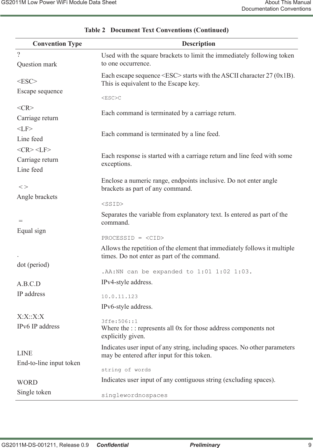
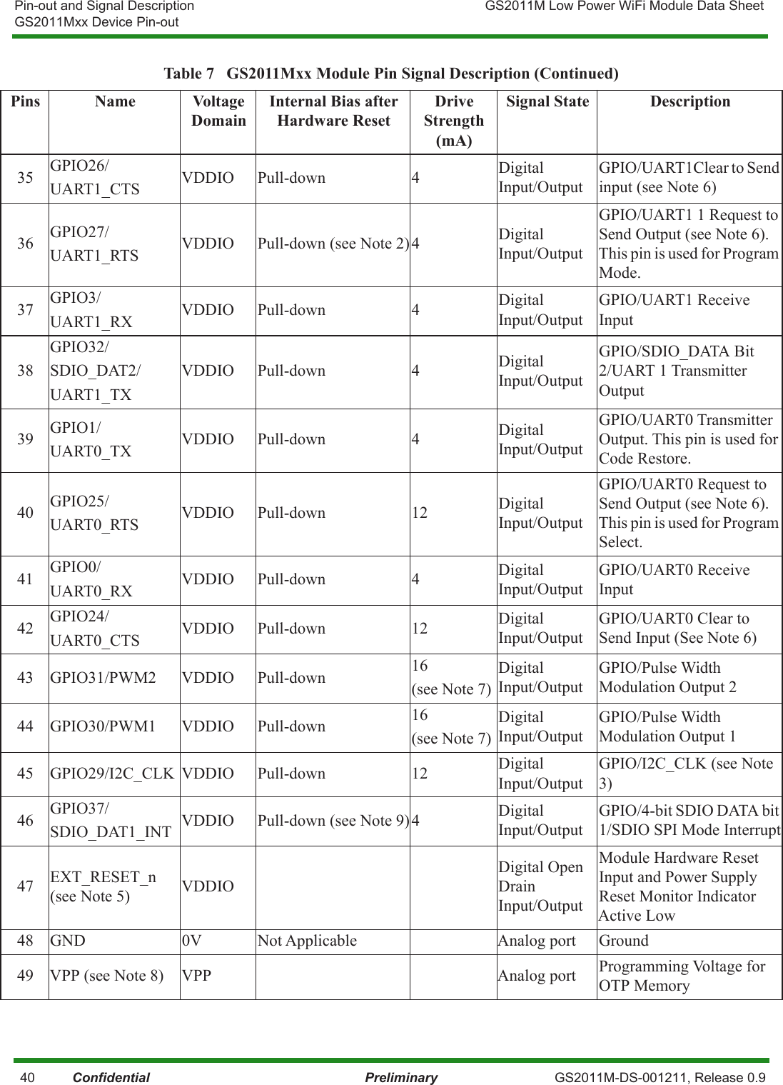
![About This Manual GS2011M Low Power WiFi Module Data SheetAudience 8 Confidential Preliminary GS2011M-DS-001211, Release 0.9AudienceThis manual is designed to help system designers build low power, cost effective, flexible platforms to add WiFi connectivity for embedded device applications using the GainSpan GS2011M based module.StandardsThe standards that are supported by the GainSpan GS module series are:– IEEE 802.11 b/g/nDocumentation ConventionsThis manual uses the following text and syntax conventions:– Special text fonts represent particular commands, keywords, variables, or window sessions– Color text indicates cross-reference hyper links to supplemental information– Command notation indicates commands, subcommands, or command elementsTable 2, page 8, describes the text conventions used in this manual for software procedures that are explained using the AT command line interface.Table 2 Document Text Conventions Convention Type Descriptioncommand syntaxmonospaced fontThis monospaced font represents command strings entered on a command line and sample source code.AT XXXXProportional fontdescriptionGives specific details about a parameter.<Data> DATAUPPERCASEVariable parameterIndicates user input. Enter a value according to the descriptions that follow. Each uppercased token expands into one or more other token.lowercaseKeyword parameterIndicates keywords. Enter values exactly as shown in the command description. [ ]Square bracketsEnclose optional parameters. Choose none; or select one or more an unlimited number of times each. Do not enter brackets as part of any command.[parm1|parm2|parm3]](https://usermanual.wiki/Gainspan/GS2011MIZ/User-Guide-2250977-Page-8.png)
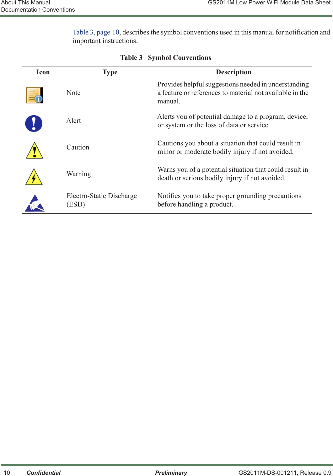
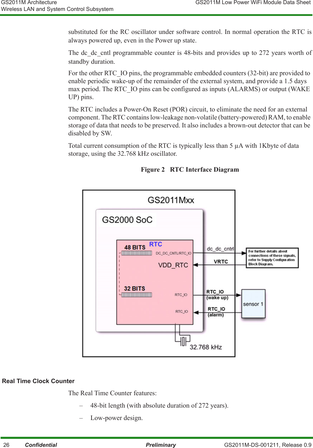
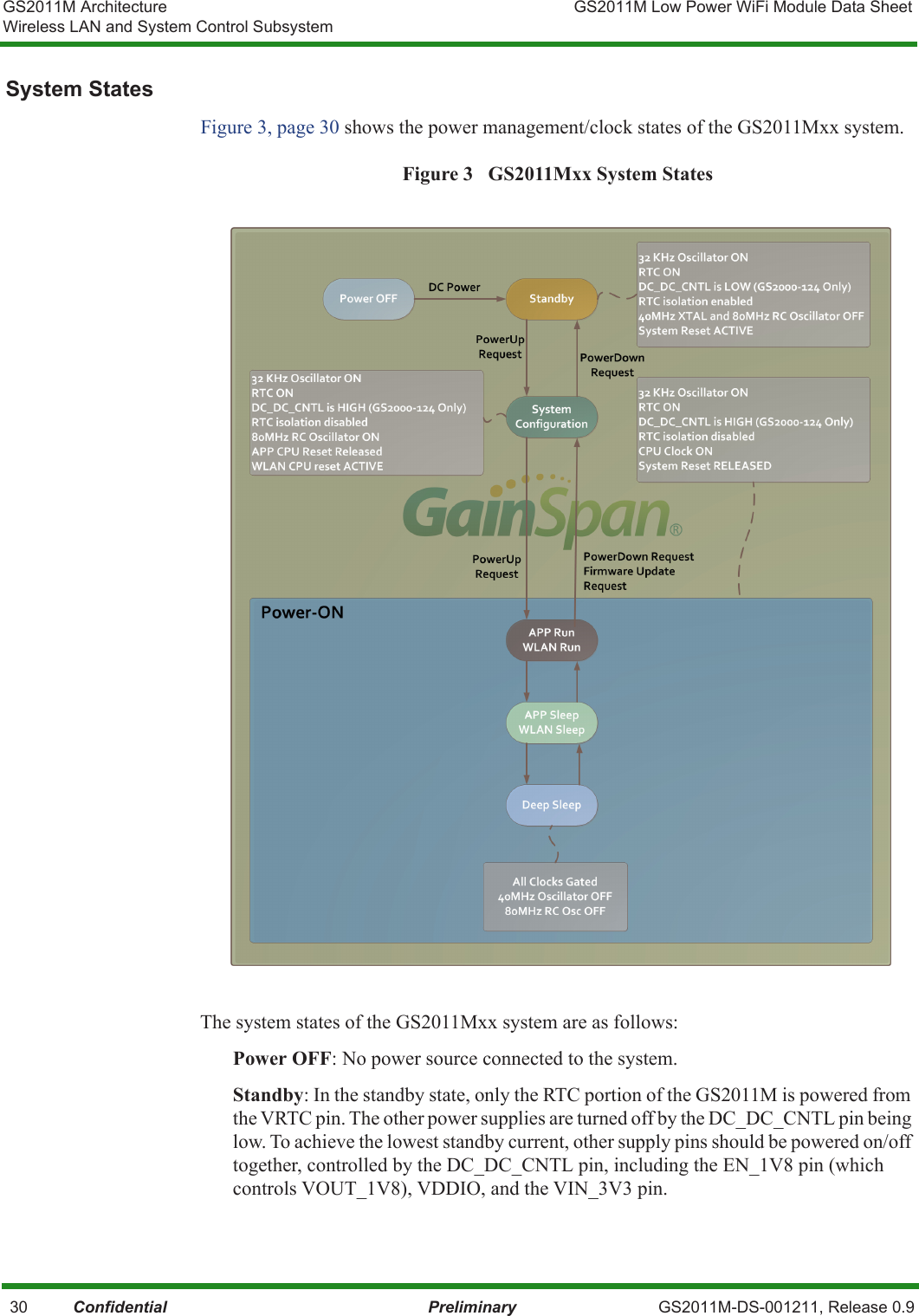
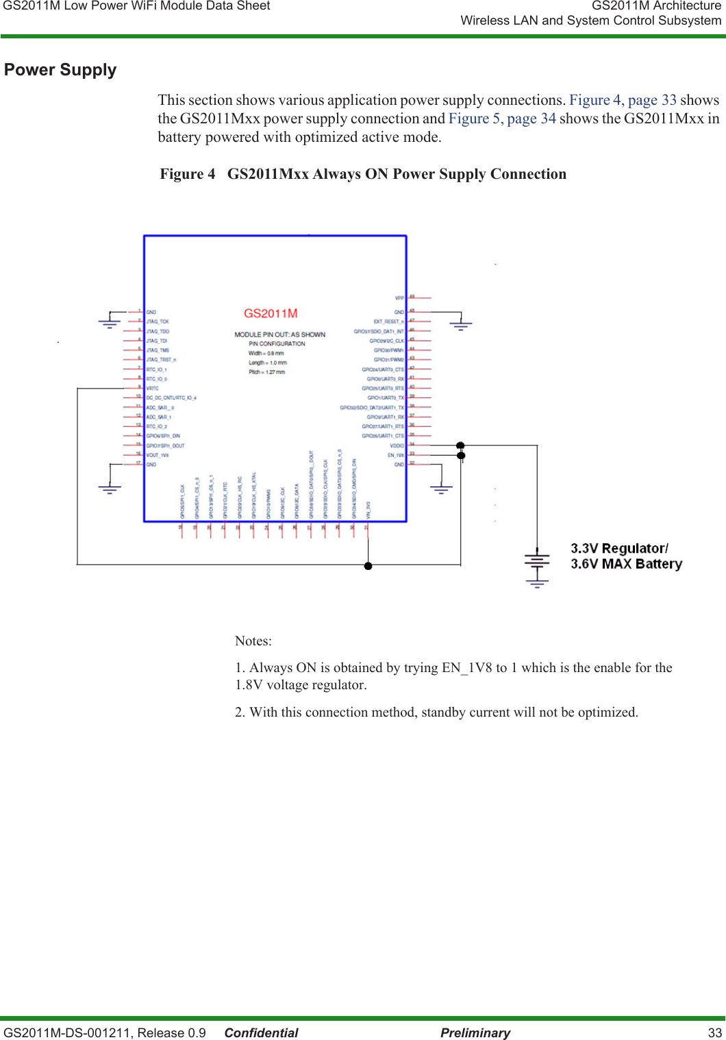
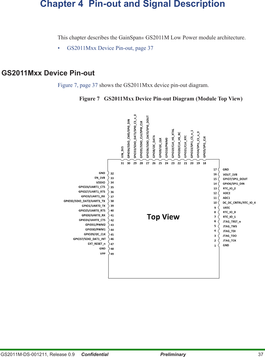
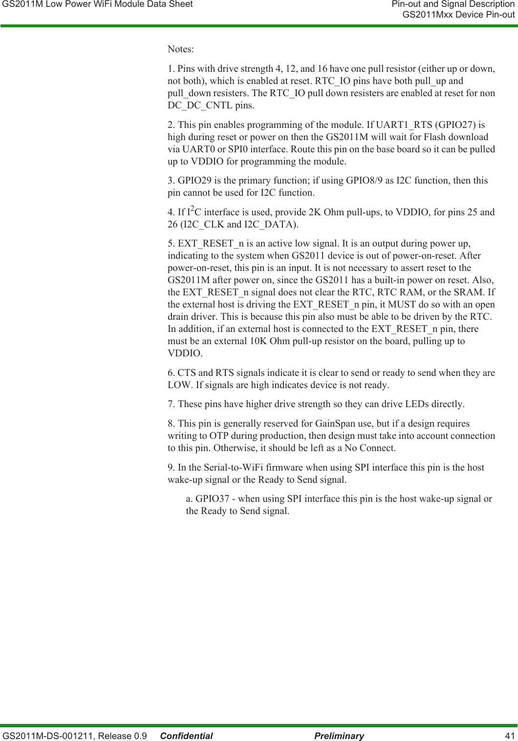
![Pin-out and Signal Description GS2011M Low Power WiFi Module Data SheetGS2011Mxx Device Pin-out 42 Confidential Preliminary GS2011M-DS-001211, Release 0.9GS2011M Pin MUX FunctionThe GS2011M pins have multiple functions that can be selected using MUX function by software. Each pin has an independent MUX select register. Table 8, page 42 shows the various MUX functions for each pin. All pins are GPIO inputs at reset. For pins that are inputs to functional blocks only one pin may be assigned to any input function. For example, UART1_RX may be assigned to GPIO3 but not to both GPIO3 and GPIO37.Table 8 GS2011M Pin MUX Description Pin# Pin Name Mux3 Mux4 Mux5 Mux6 Mux7 Comments1 GND2 jtag_tck3 jtag_tdo4 jtag_tdi5 jtag_tms6 jtag_trst_n7 rtc_io_18 rtc_io_09VRTC10 dc_dc_cntl/rtc_io_411 adc_sar_012 adc_sar_113 rtc_io_214 gpio6/spi1_din spi1_din wspi_din spi1_dout wspi_dout spi0_cs_n_115 gpio7/spi1_dout spi1_dout wspi_dout spi1_din wspi_din spi0_cs_n_216 VOUT_1V817 GND18 gpio5/spi1_clk spi1_clk wspi_clk pwm0 traceclk spi0_cs_n_319 gpio4/spi1_cs_n_0 spi1_cs_n_0 wspi_cs_n_0 spi0_cs_n_4 reserved clk_rtc20 gpio13/spi1_cs_n_1 spi1_cs_n_1 pwm2 spi0_cs_n_5 tracedata[0] wspi_cs_n_121 gpio21/clk_rtc clk_rtc spi1_cs_n_2 clk_hs_xtal tracedata[1] spi0_cs_n_622 gpio20/clk_hs_rc clk_hs_rc spi1_cs_n_3 clk_hs_xtal tracedata[2] spi0_cs_n_723 gpio19_clk_hs_xtal clk_hs_xtal gpi1_cs_n_4 pwm2 tracedata[3] spi0_cs_n_824 gpio10/pwm0 pwm0 reserved reserved tracedata[0] clk_rtc25 gpio9/i2c_clk i2c_clk uart1_rx reserved tracedata[1] i2s_lcrclk26 gpio8/i2c_data i2c_data uart1_tx reserved tracedata[3] reserved27 gpio36/sdio_dat0/spi0_dout sdio_data0 reserved i2c_data reserved spi0_dout28 gpio35/sdio_clk/spi0_clk sdio_clk reserved i2c_clk traceclk spi0_clk Note: only 4mA for i2c29 gpio33/sdio_dat3/spi0_cs_n_0 sdio_data3 reserved uart1_rts tracedata[0] spi0_cs_n_030 gpio34/sdio_cmd/spi0_din sdio_cmd reserved uart1_cts tracedata[1] spi0_din](https://usermanual.wiki/Gainspan/GS2011MIZ/User-Guide-2250977-Page-42.png)
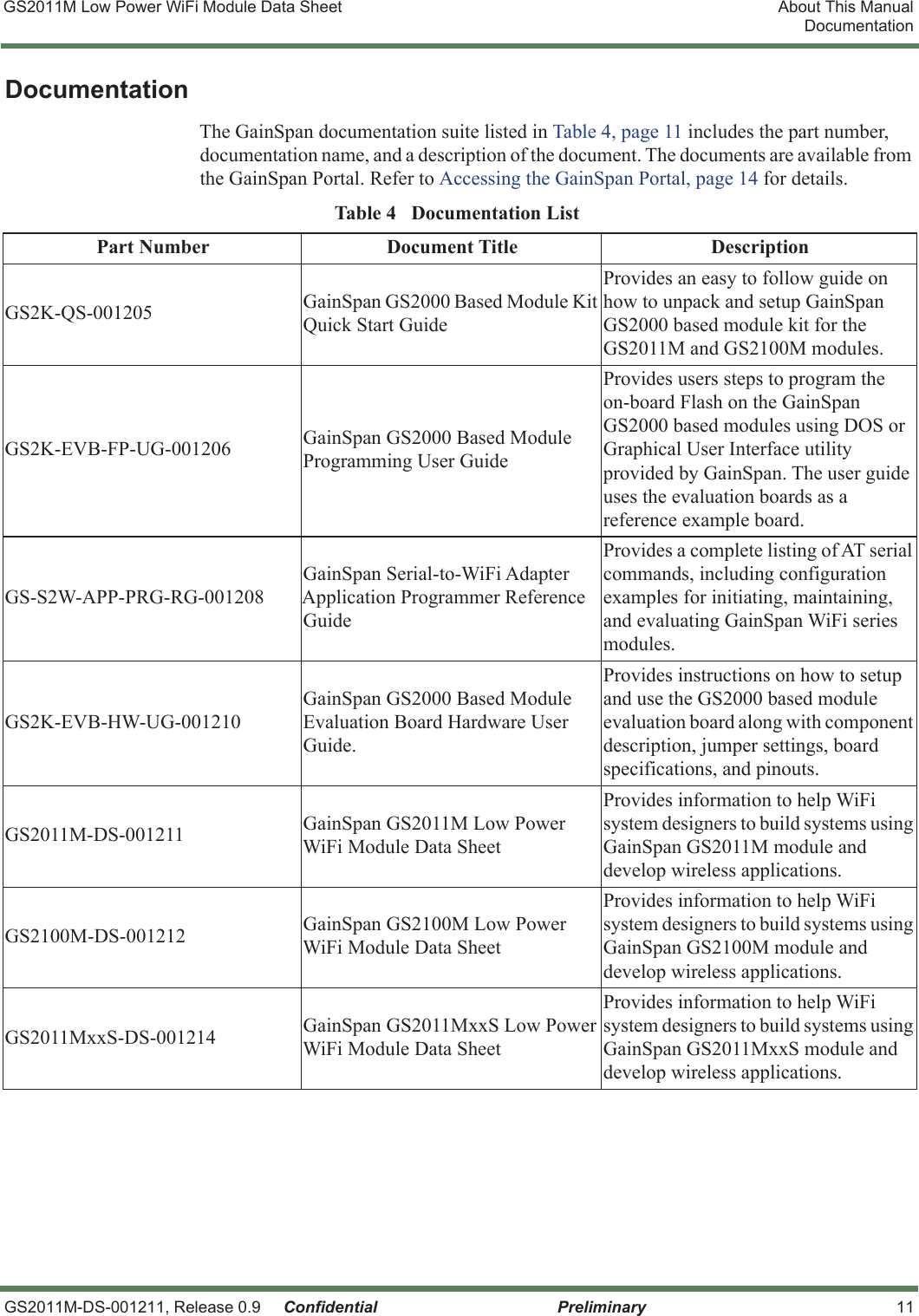
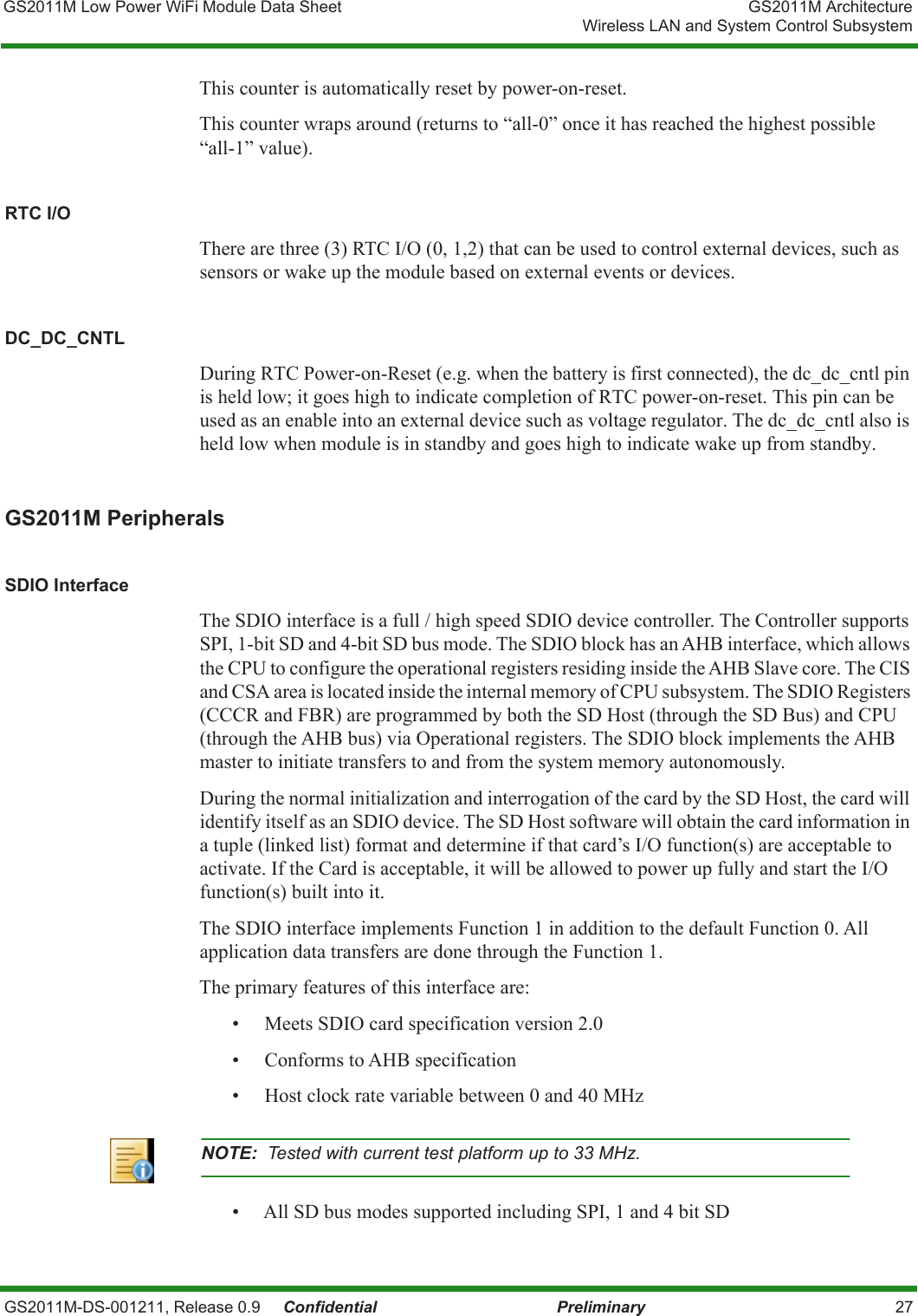
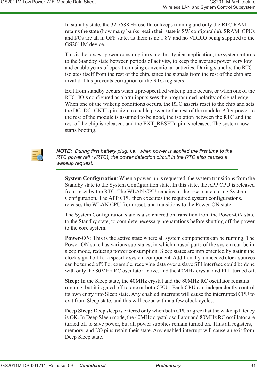
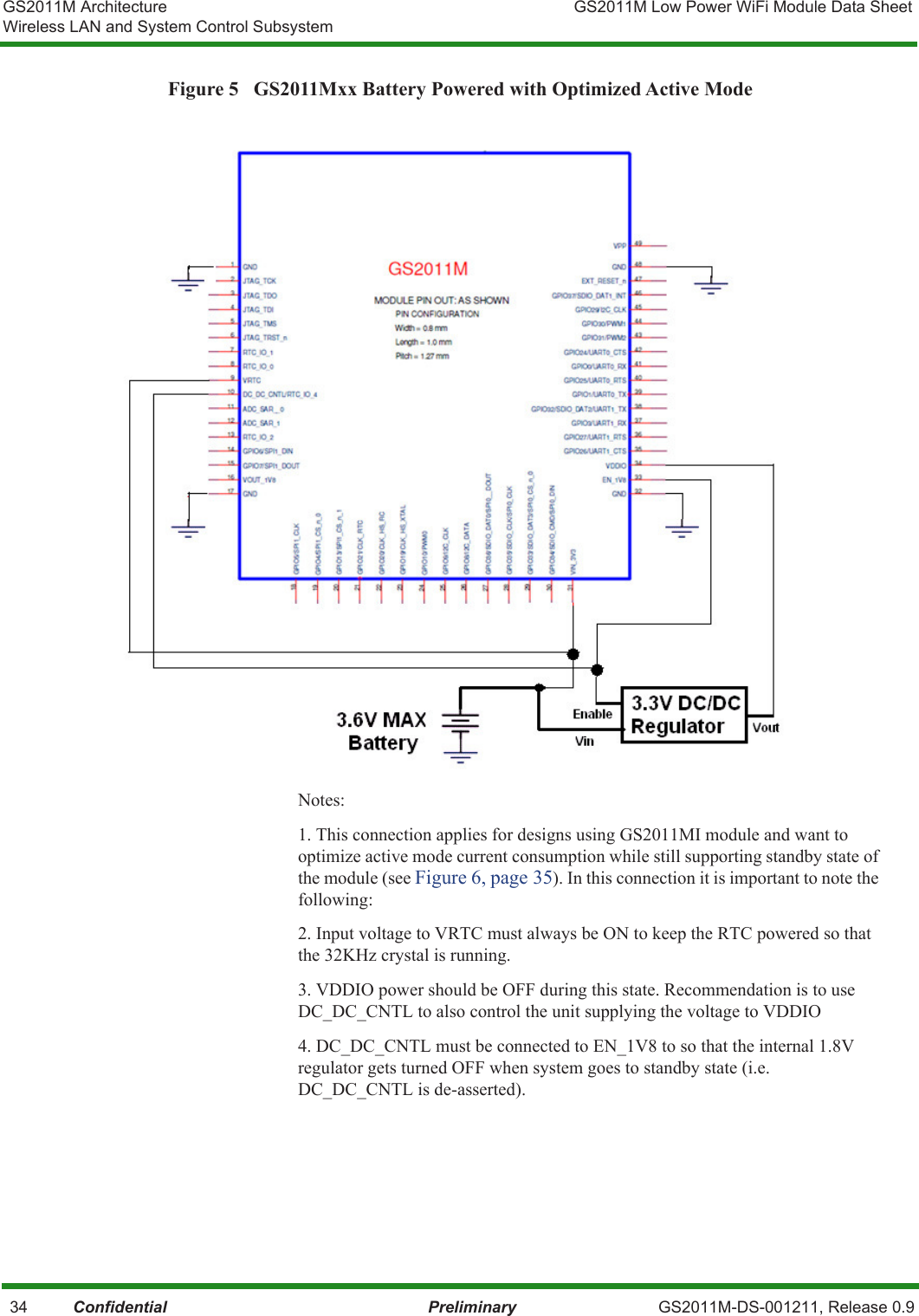
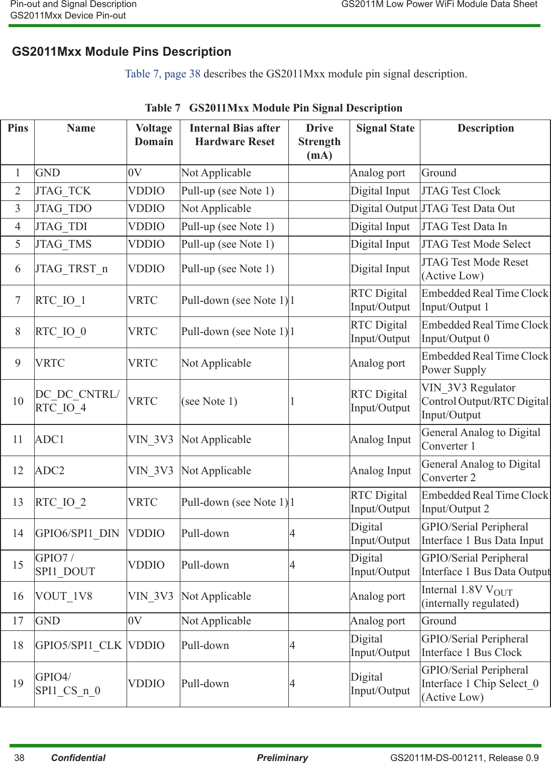
![GS2011M Low Power WiFi Module Data Sheet Pin-out and Signal DescriptionGS2011Mxx Device Pin-outGS2011M-DS-001211, Release 0.9 Confidential Preliminary 4331 VIN_3V3 Includes Flash, PA, ADC, VDDIO, REG32 GND33 EN_1V834 VDDIO35 gpio26/uart1_cts uart1_cts wuart_cts i2s_din spi1_cs_n_13 wssp_clk36 gpio27/uart1_rts uart1_rts wuart_rts i2s_dout uart1_tx wspi_dout37 gpio3/uart1_rx uart1_rx wuart_rx i2s_bitclk spi1_cs_n_14 wsip_din38 gpio32/sdio_dat2/uart1_tx sdio_data1 wuart_tx uart1_tx tracedata[2] spi1_cs_n_1239 gpio1/uart0_tx uart0_tx wuart_tx pwm1 tracedata[0] spi1_dout40 gpio25/uart0_rts uart0_rts wuart_rts reserved tracedata[1] spi1_clk41 gpio24/uart0_cts uart0_rx wuart_rx pwm2 tracedata[2] spi1_din42 gpio24/uart0_cts uart0_cts wuart_cts reserved tracedata[3] spi1_cs_n_043 gpio31/pwm2 pwm2 spi1_dout usart1_tx traceclk wuart_tx44 gpio30/pwm1 pwm1 spi1_din uart1_rx reserved wuart_rx45 gpio29/i2c_clk i2c_clk spi1_cs_n_20 clk_rtc tracedata[0] pwm046 gpio37/sdio_dat1_int sdio_data1 wuart_rx uart1_rx tracedata[3] spi0_cs_n_1047 ext_reset_n48 GND49 VPP Programming voltage for OTP memoryTable 8 GS2011M Pin MUX Description (Continued)Pin# Pin Name Mux3 Mux4 Mux5 Mux6 Mux7 Comments](https://usermanual.wiki/Gainspan/GS2011MIZ/User-Guide-2250977-Page-43.png)