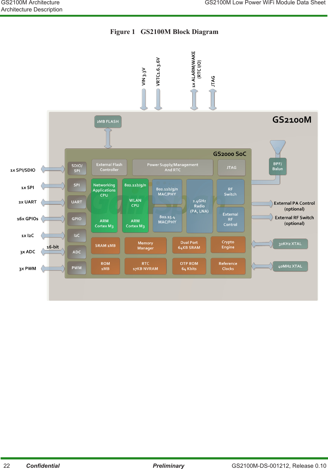
Gainspan GS2100MIE Ultra-Low Power Wi-Fi Module User Manual
Gainspan Corporation Ultra-Low Power Wi-Fi Module
UserManual.wiki
>
Gainspan
>
GS2100MIE User Manual
>
Users Manual
Contents
1.
Users Manual
2.
User Manual
Users Manual
Navigation menu
Upload a User Manual
Namespaces
Wiki Guide
HTML
PDF
Info
Views
User Manual
Discussion / Help
Navigation
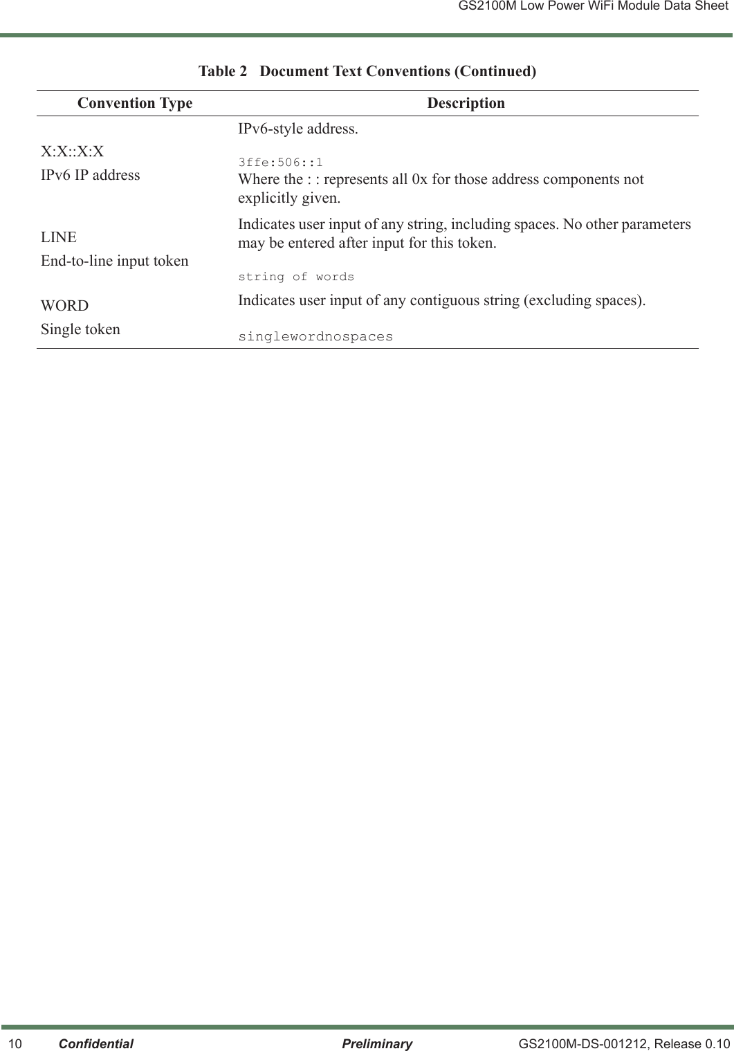
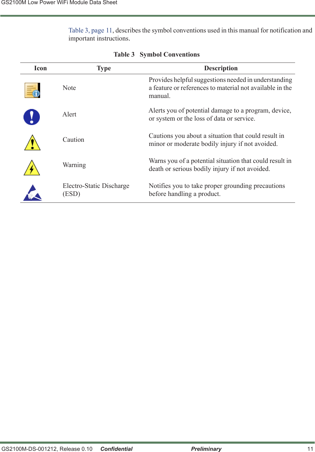
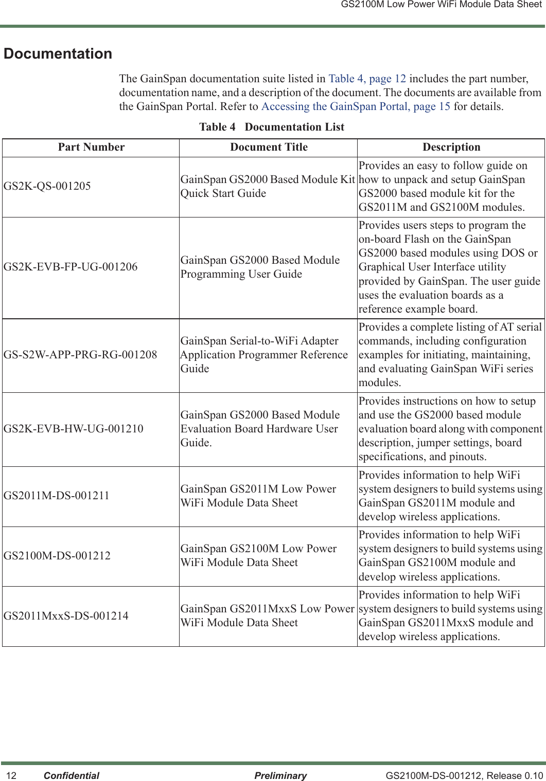
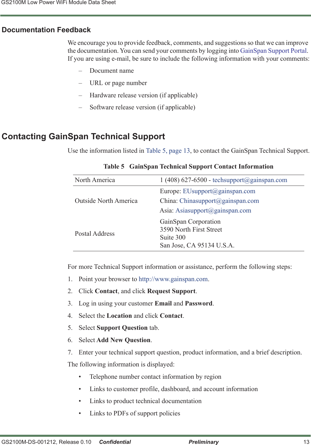
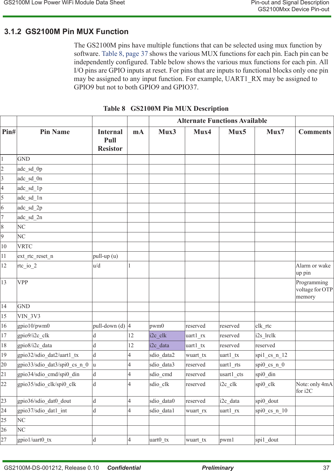
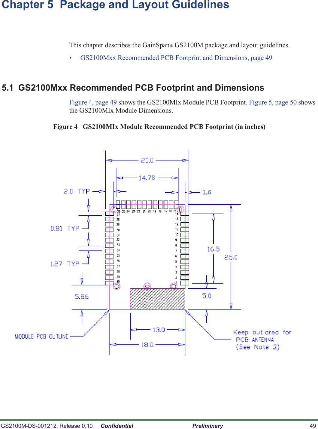
![GS2100M Low Power WiFi Module Data SheetGS2100M-DS-001212, Release 0.10 Confidential Preliminary 9UPPERCASEVariable parameterIndicates user input. Enter a value according to the descriptions that follow. Each uppercased token expands into one or more other token.lowercaseKeyword parameterIndicates keywords. Enter values exactly as shown in the command description. [ ]Square bracketsEnclose optional parameters. Choose none; or select one or more an unlimited number of times each. Do not enter brackets as part of any command.[parm1|parm2|parm3]?Question markUsed with the square brackets to limit the immediately following token to one occurrence.<ESC>Escape sequenceEach escape sequence <ESC> starts with the ASCII character 27 (0x1B). This is equivalent to the Escape key.<ESC>C<CR>Carriage return Each command is terminated by a carriage return.<LF>Line feed Each command is terminated by a line feed.<CR> <LF>Carriage returnLine feedEach response is started with a carriage return and line feed with some exceptions. < >Angle bracketsEnclose a numeric range, endpoints inclusive. Do not enter angle brackets as part of any command.<SSID> =Equal signSeparates the variable from explanatory text. Is entered as part of the command.PROCESSID = <CID>.dot (period)Allows the repetition of the element that immediately follows it multiple times. Do not enter as part of the command..AA:NN can be expanded to 1:01 1:02 1:03.A.B.C.DIP addressIPv4-style address.10.0.11.123Table 2 Document Text Conventions (Continued)Convention Type Description](https://usermanual.wiki/Gainspan/GS2100MIE.Users-Manual/User-Guide-2302631-Page-9.png)