Garmin Canada 1695 LOW POWER COMMUNICATIONS TRANSMITTER User Manual o6r1695 UserMan
DynaStream Innovations Inc. LOW POWER COMMUNICATIONS TRANSMITTER o6r1695 UserMan
Users Manual
P +1 403.932.4620 F +1 403.932.6521
AP2 RF Transceiver Module
FEATURES
• 2.4GHz worldwide ISM band
• 78 selectable RF channels (2403 to 2480MHz)
• 20mm x 20mm drop-in module
• Ultra low power operation
• Simple sync/async serial interface
• Integrated F antenna
• On board 32.768 kHz crystal oscillator
• Broadcast, acknowledged, or burst data transmissions
• ANT channel combined message rate up to 190Hz (8byte data
payload)
• Minimum message rate per ANT channel 0.5Hz
• Burst transfer rate up to 20Kbps (true data throughput)
• Up to 8 ANT channels
• Up to 3 public, managed and/or private network keys
• 1 Mbps RF data rate
• 1.9V to 3.6V supply voltage range
• -40°C to +85°C operating temperature
• Pin compatible with AP1 and AT3 modules
• Radio regulatory approval for major markets (pending)
• RoHS compliant
FAMILY MEMBERS
ANTAP281M4IB – 8 ANT channels; surface mount
ANTAP281M5IB – 8 ANT channels; Molex connector
ANT NETWORK CONFIGURATIONS
112
211
310
4 9
5 8
6 7
M
PEER
TO
PEER
STAR
PRACTICAL MESH
SHARED
BI-DIRECTIONAL
8 7 6
9
10
11
12
13
14 15 16
5
4
3
2
1
SCANNING MODE
ANT-FS
(Secure Authenticated)
112
211
310
4 9
?8
6 7
M
AD-HOC
AUTO
SHARED
112
211
310
4 9
5 8
6 7
M
SHARED
UNI-DIRECTIONAL
n
Bidirectional
Acknowledged
BROADCAST
SHARED CLUSTER
Sensor
Hub
Relay
D00001266 Rev1.3

2 of 19 AP2 RF Transceiver Module
228 River Avenue, Cochrane, Alberta, Canada T4C 2C1 thisisant.com
TABLE OF CONTENTS
NOTICES AND RESTRICTED USE INFORMATION ............................................................................................ 3
ANT™ OVERVIEW ............................................................................................................................................. 4
1 ANT AP2 MODULE ................................................................................................................................... 5
1.1 INTERFACE .................................................................................................................................................. 5
1.2 APPLICATION MCU CONNECTION ...................................................................................................................... 6
1.2.1
Async Mode ..................................................................................................................................... 6
1.2.2
Byte Sync Mode ............................................................................................................................... 7
1.2.3
Bit Sync Mode .................................................................................................................................. 8
1.3 MOUNTING GUIDELINE ................................................................................................................................... 8
1.4 REFLOW GUIDELINE ...................................................................................................................................... 9
2 REGULATORY APPROVAL .....................................................................................................................10
2.1 UNITED STATES .......................................................................................................................................... 10
2.2 INDUSTRY CANADA COMPLIANCE .................................................................................................................... 10
2.3 CE DECLARATION OF CONFORMITY ................................................................................................................. 11
2.4 JAPAN ...................................................................................................................................................... 11
2.5 AUSTRALIA & NEW ZEALAND ......................................................................................................................... 11
3 ELECTRICAL SPECIFICATIONS ............................................................................................................12
4 MECHANICAL DRAWINGS ....................................................................................................................16
5 TECHNICAL SUPPORT ..........................................................................................................................19
5.1 ANT FORUM .............................................................................................................................................. 19
5.2 PUBLIC TECHNICAL REFERENCES ..................................................................................................................... 19
5.3 ANT DEVELOPER’S ZONE .............................................................................................................................. 19

AP2 RF Transceiver Module 3 of 19
228 River Avenue, Cochrane, Alberta, Canada T4C 2C1 thisisant.com
Notices and Restricted Use Information
Information contained in this document is provided only for your ("Customer" or “you”) convenience and may be
superseded by updates. It is your responsibility to ensure that your application meets with your specifications.
Dynastream Innovations Inc. ("DYNASTREAM") makes no representations or warranties of any kind whether
express or implied, written or oral, statutory or otherwise, related to the information, including but not limited
to its condition, quality, performance, merchantability or fitness for purpose. DYNASTREAM disclaims all liability
arising from this information and its use.
DYNASTEAM does not assume any responsibility for the use of the described ANT RF module (“the Module(s)”).
Dynastream makes no representation with respect to the adequacy of the module in low-power wireless data
communications applications or systems. Any Products using the Module must be designed so that a loss of
communications due to radio interference or otherwise will not endanger either people or property, and will not
cause the loss of valuable data. DYNASTREAM assumes no liability for the performance of products which are
designed or created using the Modules.
The Modules are not designed, intended, or authorized for use as components in systems intended for surgical
implant into the body, or other applications intended to support or sustain life, or for any other application in
which the failure of the Module could create a situation where personal injury or death may occur. If you use
the Modules for such unintended and unauthorized applications, you do so at your own risk and you shall
indemnify and hold DYNASTREAM and its officers, employees, subsidiaries, affiliates, and distributors harmless
against all claims, costs, damages, and expenses, and reasonable attorney fees arising out of, directly or
indirectly, any claim of personal injury or death associated with such unintended or unauthorized use, even if
such claim alleges that DYNASTREAM was negligent regarding the design or manufacture of the Product.
The information disclosed herein is the exclusive property of DYNASTREAM, and is not to be reproduced and/or
distributed without the written consent of DYNASTREAM. No part of this publication may be reproduced or
transmitted in any form or by any means including electronic storage, reproduction, execution or transmission
without the prior written consent of DYNASTREAM. The recipient of this document by its retention and use
agrees to respect the security status of the information contained herein.
DYNASTREAM believes the information contained herein is correct and accurate at the time of its release.
However, the information contained in this document is subject to change without notice and should not be
construed as a commitment by DYNASTREAM unless such commitment is expressly given in a covering
document.
©2009 Dynastream Innovations Inc. All Rights Reserved. ANT is a registered trade mark of Dynastream
Innovations Inc.
4 of 19 AP2 RF Transceiver Module
228 River Avenue, Cochrane, Alberta, Canada T4C 2C1 thisisant.com
ANT™ Overview
ANT™ is a practical wireless sensor network protocol running on 2.4 GHz ISM band. Designed for ultra low
power, ease of use, efficiency and scalability, ANT easily handles peer-to-peer, star, tree and practical
mesh topologies. ANT provides reliable data communications, flexible and adaptive network operation and
cross-talk immunity. ANT’s protocol stack is extremely compact, requiring minimal microcontroller
resources and considerably reducing system costs.
ANT provides carefree handling of the Physical, Network, and Transport OSI layers. In addition, it
incorporates key low-level security features that form the foundation for user-defined, sophisticated,
network-security implementations. ANT ensures adequate user control while considerably lightening
computational burden in providing a simple yet effective wireless networking solution.
ANT supports public, managed and private network architectures with 232 uniquely addressable devices
possible, ensuring that each device can be uniquely identified from each other in the same network.
ANT is proven with an installed base of over four million nodes in ultra low power sensor network
applications in sport, fitness, home and industrial automation. The ANT solutions are available in chips,
chipsets and modules to suit a wide variety of application needs.
Incorporated in AP2 product family are several ANT core stack enhancements:
• Background scanning
• Continuous scanning mode
• High density node support
• Improved channel search
• Channel ID management
• Improved transmission power control
• Frequency agility
• Proximity acquisition
The complete description of ANT message protocol is found in the document “ANT Message Protocol and
Usage”. The serial interface details are provided in the document “Interfacing with ANT General Purpose
Chipsets and Modules”. Both documents are available on www.thisisant.com.
Application / Presentation
Layers
Higher Level Security
Network / Transport &
Low Level Security
Data Link Layer
Physical Layer }Implemented
by ANT
}User Defined
AP2 RF Transceiver Module 5 of 19
228 River Avenue, Cochrane, Alberta, Canada T4C 2C1 thisisant.com
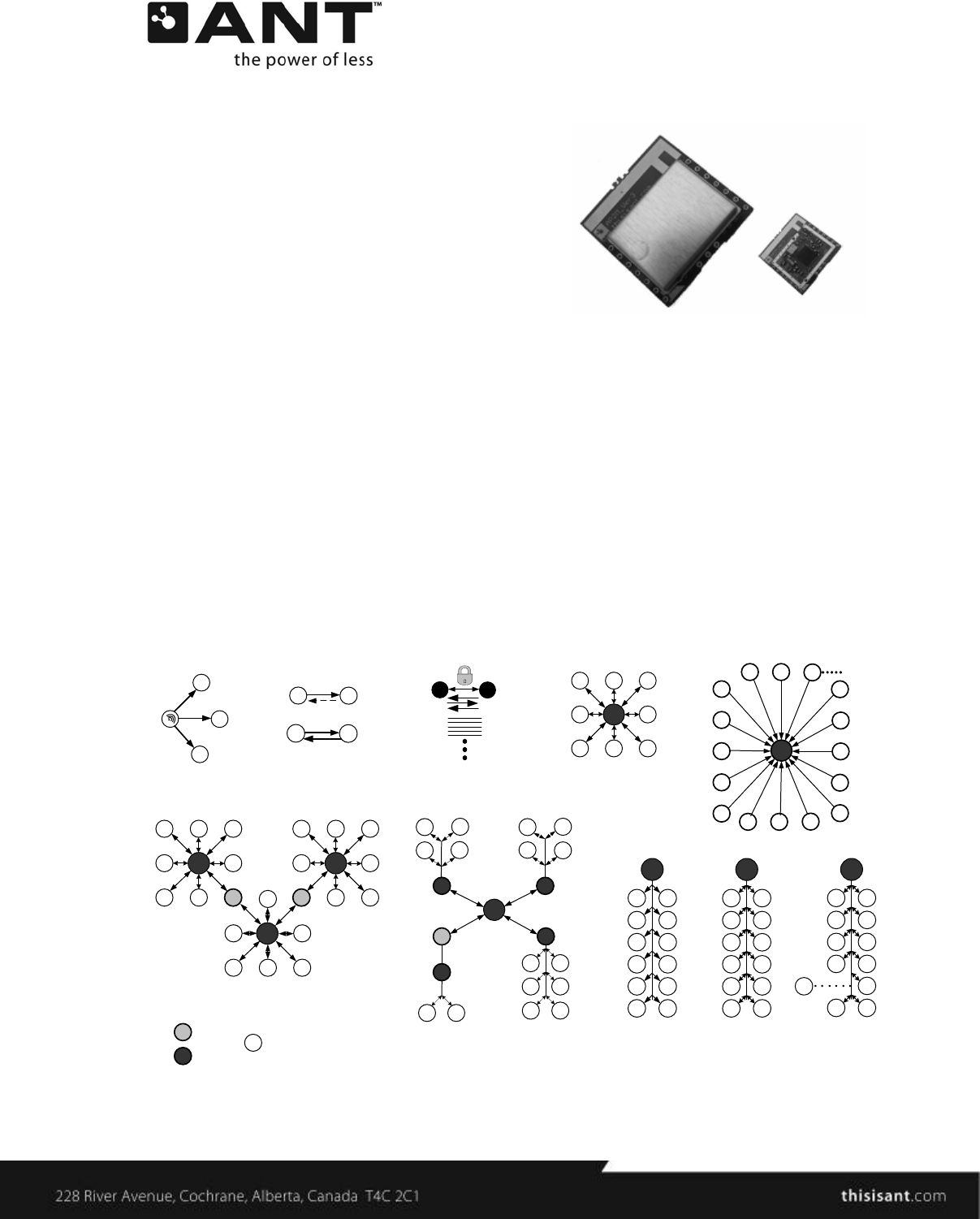
1 ANT AP2 Module
The ANT AP2 module is a drop-in module based on the reference design of nRF24AP2, a new generation of
ANT system on chip family from Nordic Semiconductor. An F antenna is integrated on the small-sized
20mm by 20mm board. The module has been certified to comply with radio regulation or standards
covering global markets include North America, Europe, Japan and Australia. The integrated module eases
the burden for application and system developers from extensive RF and antenna design, and regulatory
compliance testing, allowing quicker time to market. Able to support 8 ANT channels, the module is ideal
to build control or hub nodes of a wireless sensor network.
AP2 modules are currently available in the following varieties.
Module
A
NT chip
Used Description
ANTAP281M4IB nRF24AP2-8ch Surface mountable, 8 ANT channels, 20x20mm, industrial
temperature range
ANTAP281M5IB nRF24AP2-8ch With Molex connector, 8 ANT channels, 20x20mm, industrial
temperature range
1.1 Interface
The module may be connected to the user’s host controller using the 17 pin-out assignment (surface
mount) style or the 20-pin Molex header connection style provided below:
Surface
Mount Pin
Molex
Header Pin Pin Name Async Mode Sync Mode Description
1 6 TEST
TEST (Tie to
GND)
TEST (Tie
to GND) Tie to Ground
2 10 RST RST RST Reset the device
3 1 VCC VCC VCC Power supply source
4 19 GND GND GND Power supply ground
5 8 NC NC NC No connection
6 17
SUSPEND
/SRDY
SUSPEND SRDY Async -> Suspend control
Sync -> Serial port ready
7 15 SLEEP/ MRDY SLEEP MRDY Async -> Sleep mode enable
Sync -> Message ready indication
8 13 NC NC NC No connection
9 11 PORTSEL PORTSEL
(Tie to GND)
PORTSEL
(Tie to VCC)
Asynchronous or synchronous port
select
10 7 BR2/SCLK
BR2 SCLK Async -> Baud rate selection
Sync -> Clock output signal
11 4 TXD0/SOUT TXD0 SOUT Async -> transmit data signal
Sync -> Data output
12 3 RXD0/SIN RXD0 SIN Async -> Receive data signal
Sync -> Data input
13 5 BR1/SFLOW BR1 SFLOW
Async -> Baud rate selection
Sync -> Bit or byte flow control
select
14 9 BR3 BR3 Tie to GND Async -> Baud rate selection
Sync - > Not used, tie to ground
15 14 RESERVERD2 Tie to GND Tie to GND Reserved Pin, Tie to ground
16 12 RESERVERD1 Tie to GND Tie to GND Reserved Pin, Tie to ground
17 2 RTS/SEN RTS SEN Async -> Request to send
Sync -> Serial enable signal
16,18,20 NC NC NC No connection
6 of 19 AP2 RF Transceiver Module
228 River Avenue, Cochrane, Alberta, Canada T4C 2C1 thisisant.com
The baud rate of the asynchronous communication is controlled by the speed select signals BR1, BR2 and
BR3. The table below shows the relationship between the states of the speed select signals and the
corresponding baud rates.
BR3 BR2 BR1 Baud Rate
0 0 0 4800
0 1 0 19200
0 0 1 38400
0 1 1 50000
1 0 0 1200
1 1 0 2400
1 0 1 9600
1 1 1 57600
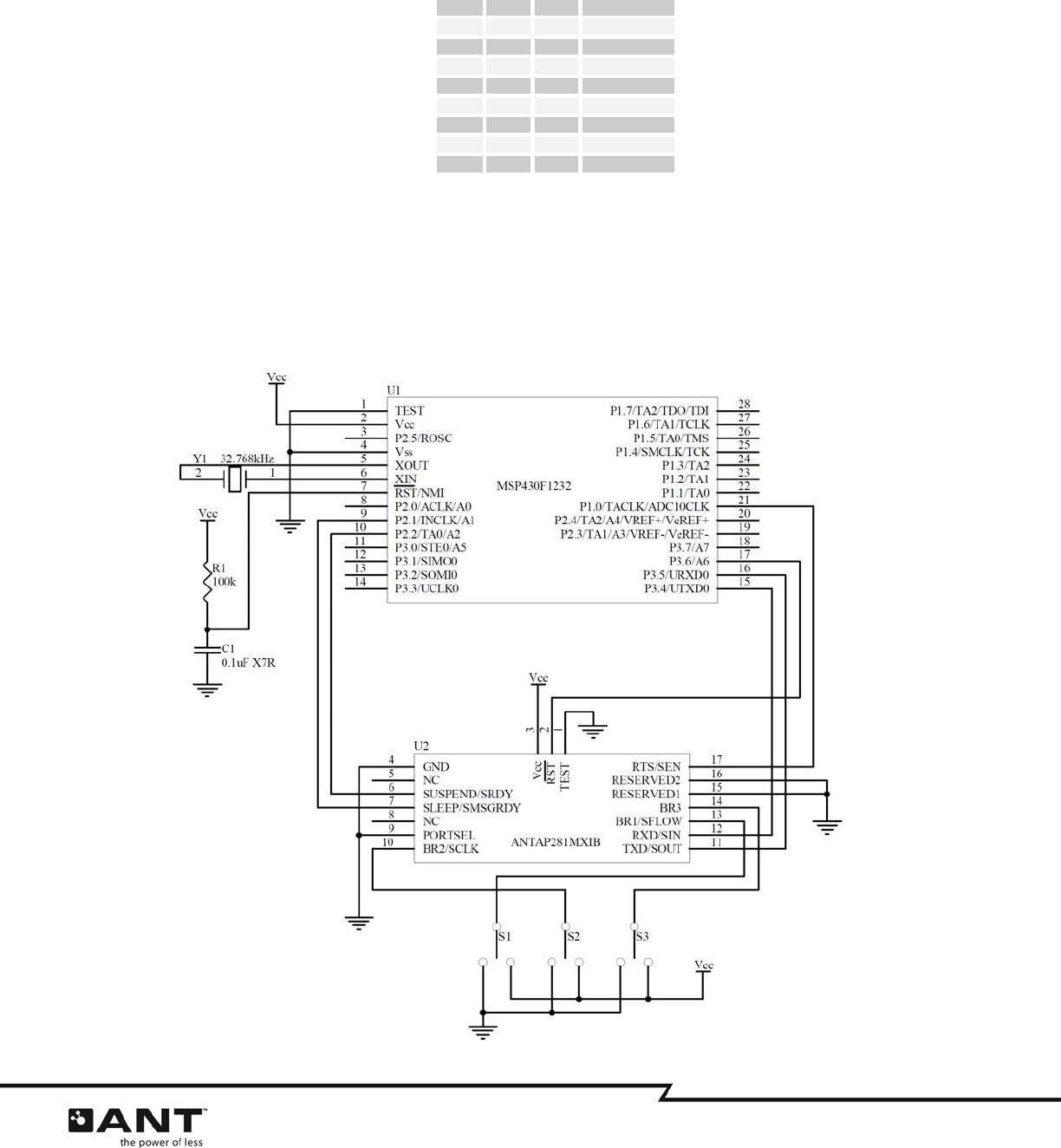
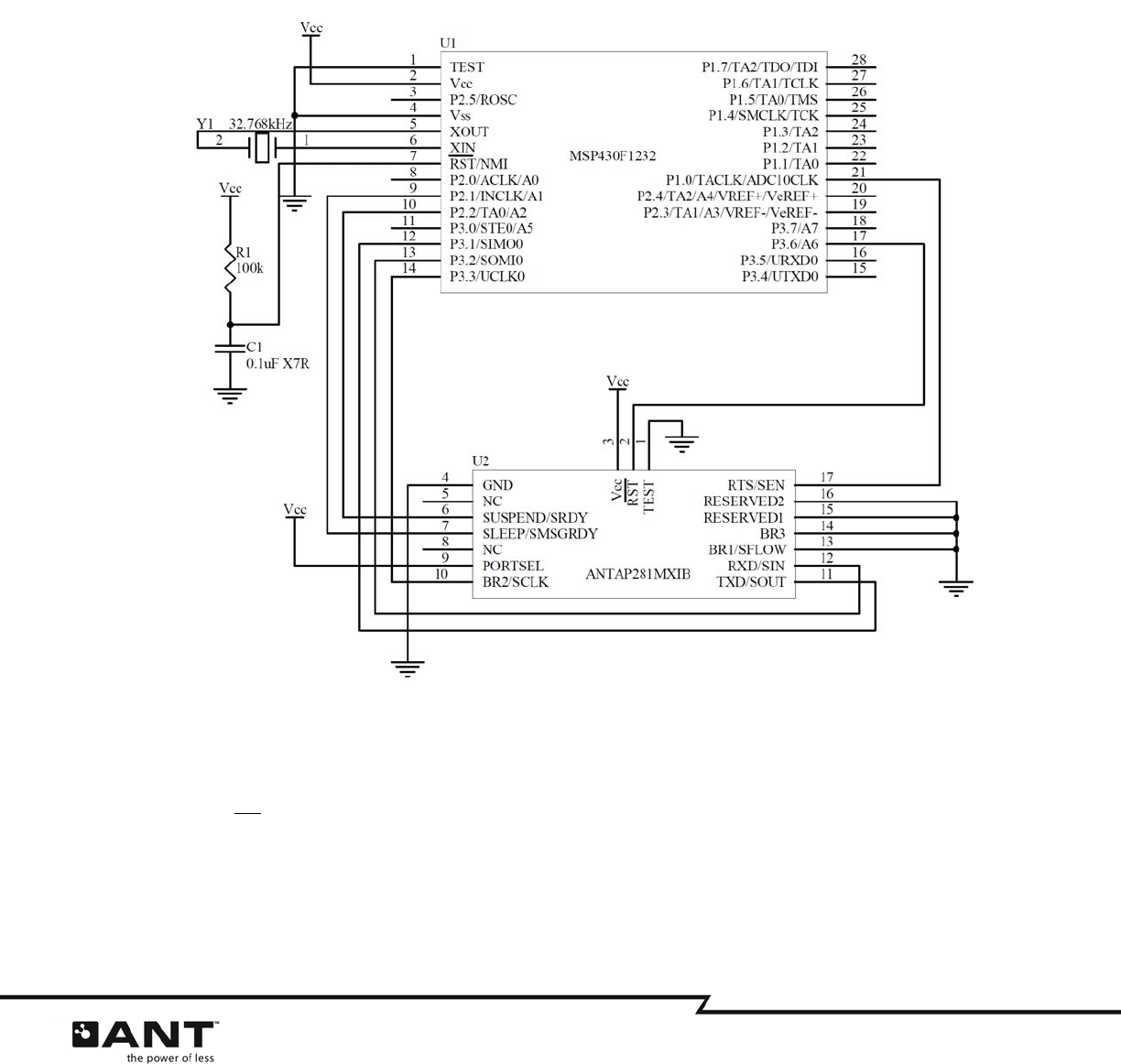
1.2 Application MCU connection
Please refer to “Interfacing with ANT General Purpose Chipsets and Modules” and “nRF24AP2 Product
Specification” section 5 “Host Interface”. The following sample designs show the proper electrical
connectivity of an ANT AP2 module to an application microcontroller, using TI MSP430F1232 as example.
1.2.1
Async Mode
AP2 RF Transceiver Module 7 of 19
228 River Avenue, Cochrane, Alberta, Canada T4C 2C1 thisisant.com
Notes:
• Module RXD and TXD connected directly to hardware USART of microcontroller.
• Switches on baud rate selection pins (BR1, BR2 and BR3) are for ease of use only. They can be
connected directly to the logic level of interest.
• RTS can be connected to an interrupt pin for convenience in some applications. (Interrupt pins
located on Port 1&2 on the MSP430F1232)
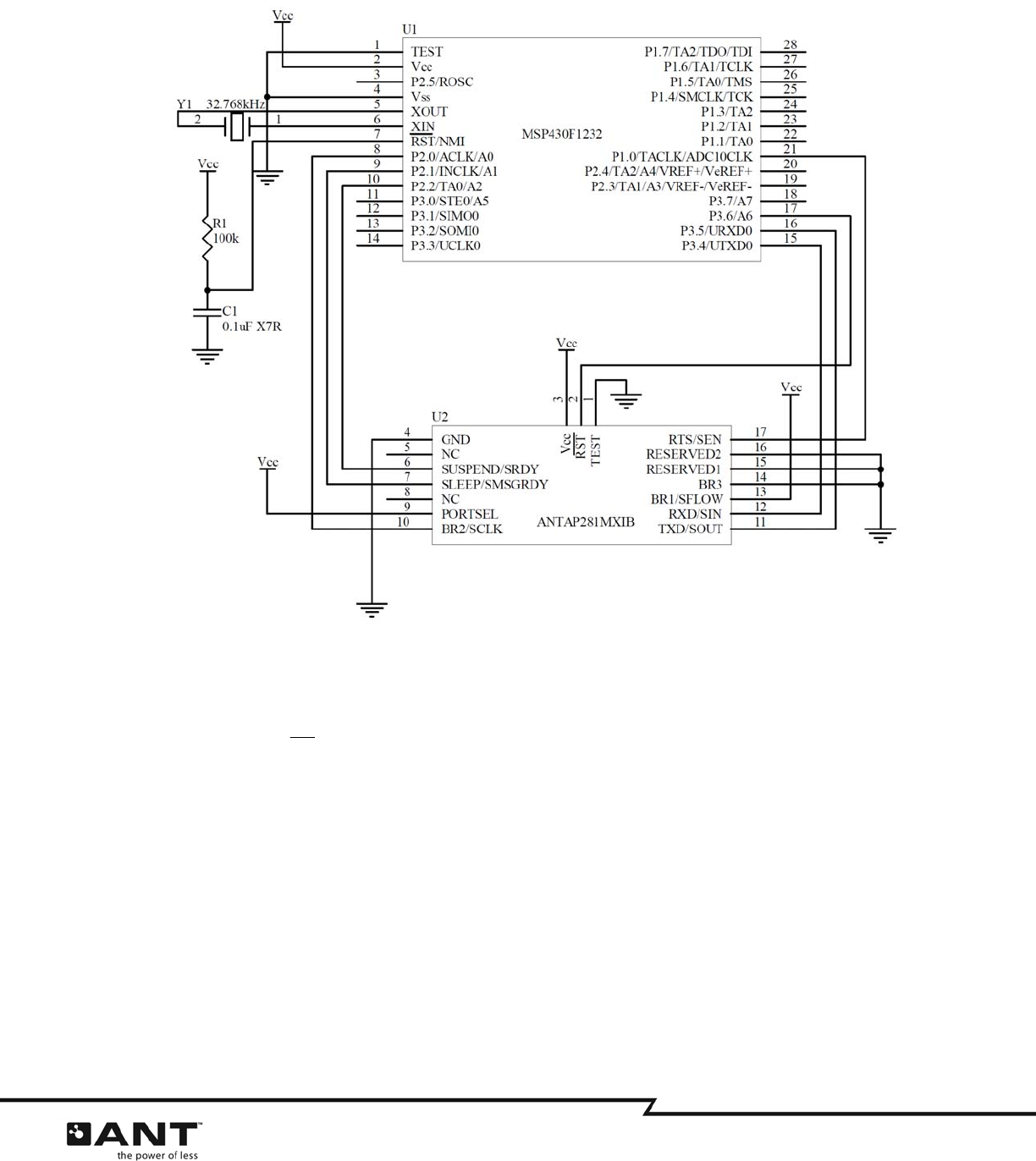
1.2.2
Byte Sync Mode
Notes:
• Module SOUT, SIN, and SCLK connected directly to hardware USART of microcontroller.
• SEN needs to be on an interrupt capable I/O pin on the microcontroller. (Interrupt pins located
on Port 1&2 on the MSP430F1232)
8 of 19 AP2 RF Transceiver Module
228 River Avenue, Cochrane, Alberta, Canada T4C 2C1 thisisant.com
1.2.3
Bit Sync Mode
Notes:
• All interface signals are connected directly to I/O pins on the microcontroller.
• SCLK and SEN need to be on an interrupt capable I/O pin on the microcontroller. (Interrupt pins
located on Port 1&2 on the MSP430F1232)
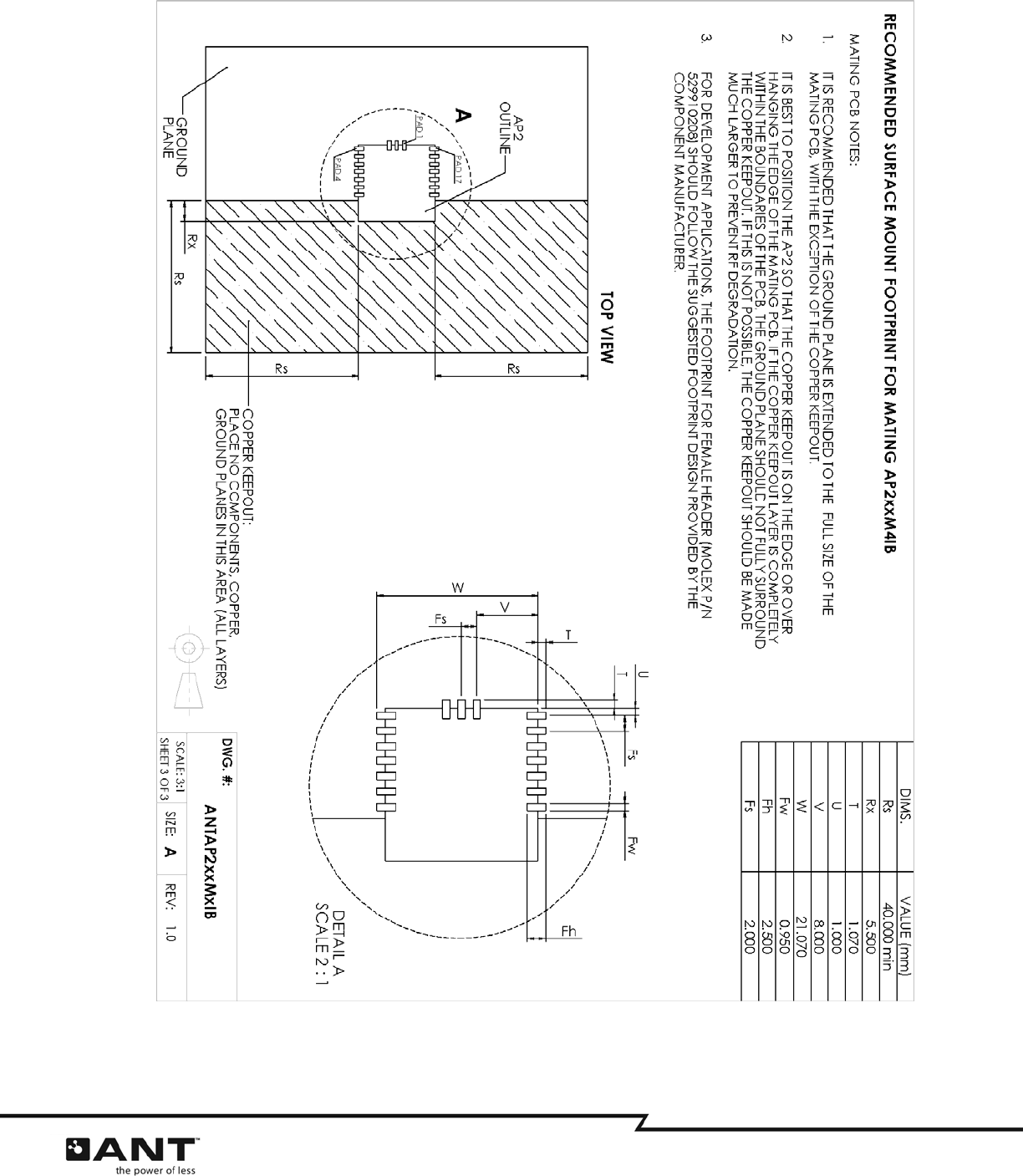
1.3 Mounting Guideline
Refer to the recommended footprint drawing in section 4.
It is best to position the AP2 module so that the copper keepout area is on the edge or over hanging the edge of the
mating PCB. If the copper keepout layer is completely within the boundaries of the PCB, the ground plane should not
fully surround the copper keepout. If this is not possible, the copper keepout should be made much larger to prevent RF
degradation. The ground plane is recommended to extend to the full size of the mating PCB, with the exception of the
copper keepout.
To connect to M5IB type of AP2 module, the mating socket is Molex 52991-0208.

AP2 RF Transceiver Module 9 of 19
228 River Avenue, Cochrane, Alberta, Canada T4C 2C1 thisisant.com
1.4 Reflow Guideline
Follow the guideline below if AP281M4IB modules go through reflow oven.
Peak solder joint/pad temperatures exceeding 240ºC are not recommended. If possible, pre-heat the
assembly within the oven profile for ~30 seconds at ~150 ºC. Follow the solder paste manufacturer’s
recommendations, especially regarding temperature ramp rate and the time above liquidus.

10 of 19 AP2 RF Transceiver Module
228 River Avenue, Cochrane, Alberta, Canada T4C 2C1 thisisant.com
2 Regulatory Approval
(When this revision of document is published, the certification testing is in process and regulatory
approvals are pending.)
The ANT AP2 module has received regulatory approvals for modular devices in the United States (FCC),
Canada (IC), Europe (ETSI), Japan (ARIB), Australia and New Zealand. Such approvals allow the user to
place the module inside a finished product and, in usual case, not require regulatory testing for an
intentional radiator, provided no changes or modifications are made to the module circuitry. This does not
preclude the possibility that some other form of authorization or testing may be required for the finished
product. Changes or modifications could void the user’s authority to operate the equipment. The end user
must comply with all of the instructions provided by the Grantee, which indicate installation and/or
operating conditions necessary for compliance.
2.1 United States
The AP2 module has been tested and found to comply with Part 15 of the FCC interference limits for Class
B devices. Operation is subject to the following two (2) conditions: 1) This device may not cause harmful
interference and 2) This device must accept any interference received including interference that may
cause undesired operation.
This equipment generates uses and can radiate radio frequency energy and may cause harmful
interference to radio communications if not installed and used in accordance with the instructions.
However, there is no guarantee that interference will not occur in a particular installation. If this
equipment does cause harmful interference to radio or television reception, which can be determined by
turning the equipment off and on, the user is encouraged to try to correct the interference by one of the
following measures:
• Reorient or relocate the receiving antenna.
• Increase the separation between the equipment and the receiver.
• Connect the equipment into an outlet that is on a different circuit from the receiver.
• Consult the dealer or an experienced radio/TV technician for help.
This product does not contain any user-serviceable parts. Unauthorized repairs or modifications could
result in permanent damage to the equipment, and void your warranty and your authority to operate this
device under Part 15 regulations.
The AP2 module is labeled with its own FCC ID, O6R1695 (note: First Character is the letter O, not the #
0.) If the FCC ID is not visible when the module is installed inside another device, then the outside of the
device into which the module is installed must also display a label referring to the enclosed module. This
exterior label can use wording such as the following: “Contains Transmitter Module FCC ID: O6R1695” or
“Contains FCC ID: O6R1695”. Any similar wording that expresses the same meaning may be used.
2.2 Industry Canada Compliance
The AP2 module has been certified for use in Canada under Industry Canada (IC) Radio standards
Specification (RSS) RSS-210 and RSS-Gen. Operation is subject to the following two conditions: (1) this
device may not cause interference, and (2) this device must accept any interference, including
interference that may cause undesired operation of the device.
To comply with Industry Canada regulations, it is required that product containing the AP2 module display
a label referring to the enclosed module. This exterior label can use wording similar to the following:
“Contains IC: 3797A-1695”
This information shall be affixed in such a manner as not to be removable except by destruction or
defacement. The size of the lettering shall be legible without the aid of magnification but is not required
to be larger than 8-point font size. If the device is too small to meet this condition, the information can be
included in the user manual upon agreement with Industry Canada.

AP2 RF Transceiver Module 11 of 19
228 River Avenue, Cochrane, Alberta, Canada T4C 2C1 thisisant.com
2.3 CE Declaration of Conformity
The AP2 module is declared to be in conformance with the essential requirements and other relevant
provisions of Directive 1999/5/EC, as a low-powered unlicensed transmitter:
• EN 60950-1:2006 Safety of Information Technology Equipment
• EN 300 440-2 v 1.1.2 Electromagnetic compatibility and Radio Spectrum Matters (ERM): Short
range devices.
• EN 301 489-3 v 1.4.1 Electromagnetic compatibility and Radio Spectrum Matters (ERM): Short
range devices.
• EN 61000-6-1 Generic Immunity Standard
2.4 Japan
The AP281M5IB module has been tested and granted certification to comply with ARIB STD-T66.
2.5 Australia & New Zealand
The AP2 module has been tested and found to comply with AS/NZS 4268:2003, Radio equipment and
systems – Short range devices.

12 of 19 AP2 RF Transceiver Module
228 River Avenue, Cochrane, Alberta, Canada T4C 2C1 thisisant.com
3 Electrical Specifications
A
bsolute Maximum Ratings
V
oltage applied at
V
CC to
V
SS -0.3V to +3.6V
Input voltage at any pin -0.3V to
V
CC + 0.3V; max +3.6V
Operating temperature -40ºC to +85ºC
Storage temperature -40ºC to +85ºC
Note: Stress exceeding one or more of the above maximum ratings may cause permanent damage.
Conditions: VCC = +3.0V, VSS = 0V, TA = - 40ºC to +85ºC
Symbol Parameter (condition) Notes Min Typ. Max Units
Operating conditions
V
CC Supply voltage 1.9 3.0 3.6
V
T
A
Operating temperature -40 +85 ºC
Digital input pin
V
IH HIGH level input voltage 0.7
V
CC
V
CC
V
V
IL LOW level input voltage
V
SS 0.3
V
CC
V
Digital output pin
VOH HIGH level output voltage (IOH=-0.5mA)
V
CC -
0.3 VCC V
V
OL LOW level output voltage (IOL=0.5mA)
V
SS 0.3
V
General RF conditions
fOP Operating frequency 1) 2400 2403-
2480 2483.5 MHz
PLLres PLL Programming resolution 1 MHz
fXTAL Crystal frequency 16 MHz
Δf Frequency deviation ±160 kHz
RGFSK Air data rate in each burst on-air 1 Mbps
FCHANNEL Non-overlapping channel spacing 1 MHz
Transmitter operation
PRF Maximum output power 2) 0 +4 dBm
PRFC RF power control range 16 18 20 dB
PRFCR RF power accuracy ±4 dB
PBW 20dB bandwidth for modulated carrier 950 1100 kHz
PRF1.1 1st adjacent channel transmit power 1MHz -20 dBc
PRF2.1 2nd adjacent channel transmit power 2MHz -40 dBc
Receiver operation
RXMAX Maximum received signal at <0.1% BER 0 dBm
RXSENS Sensitivity at 0.1% BER -85 dBm
C/ICO C/I co-channel 9 dBc
C/I1ST 1st adjacent channel selectivity C/I 1MHz 8 dBc
C/I2ND 2nd adjacent channel selectivity C/I 2MHz -20 dBc
C/I3RD 3rd adjacent channel selectivity C/I 3MHz -30 dBc
Current Consumption
IDee
p
Slee
p
Deep sleep command 0.5 µA
IIdle No active channels
–
no communications 2.0 µA
ISus
p
end Asynchronous suspend activated 2.0 µA
IBase_32kXO Base Active current (32.768 KHz crystal oscillator
or external clock source) 3.0 µA
IBase_32kSynt Base Active current (using internal synthesized
clock source) 0.1 mA
IPeakTX Peak Tx current @ 0dBm output power 3) 15 mA
IPeakTX-6 Peak Tx current @ -6dBm output power 3) 13 mA
IPeakTX-12 Peak Tx current @ -12dBm output power 3) 11 mA

AP2 RF Transceiver Module 13 of 19
228 River Avenue, Cochrane, Alberta, Canada T4C 2C1 thisisant.com
Symbol Parameter (condition) Notes Min Typ. Max Units
IPeakTX-18 Supply peak current @ -18dBm output power 3) 11 mA
IPeakRx Peak Rx current 4) 17 mA
Isearch Search current 2.9 mA
IMs
g_
Rx
_
B
y
teS
y
nc Average current / Rx message in byte sync mode 17 µA
IMs
g_
Rx
_
BitS
y
nc Average current / Rx message in bit sync mode 30 µA
IMsg_Rx_57600 Average current / Rx message in async mode at
57600 baud 20 µA
IMsg_Rx_50000 Average current / Rx message in async mode at
50000 baud 20 µA
IMsg_Rx_38400 Average current / Rx message in async mode at
38400 baud 23 µA
IMsg_Rx_19200 Average current / Rx message in async mode at
19200 baud 30 µA
IMsg_Rx_9600 Average current / Rx message in async mode at
9600 baud 48 µA
IMsg_Rx_4800 Average RF current / Rx message in async mode at
4800 baud 83 µA
IMsg_TxAck_ByteSync Average current / Acknowledged Tx message in
byte sync mode 36 µA
IMsg_TxAck_BitSync Average current / Acknowledged Tx message in bit
sync mode 48 µA
IMsg_TxAck_57600 Average current / Acknowledged Tx message in
async mode at 57600 baud 42 µA
IMsg_TxAck_50000 Average current / Acknowledged Tx message in
async mode at 50000 baud 40 µA
IMsg_TxAck_38400 Average current / Acknowledged Tx message in
async mode at 38400 baud 44 µA
IMsg_TxAck_19200 Average current / Acknowledged Tx message in
async mode at 19200 baud 55 µA
IMsg_TxAck_9600 Average current / Acknowledged Tx message in
async mode at 9600 baud 78 µA
IMsg_TxAck_4800 Average current / Acknowledged Tx message in
async mode at 4800 baud 132 µA
IMsg_RxAck_ByteSync Average current / Acknowledged Rx message in
byte sync mode 20 µA
IMsg_RxAck_BitSync Average current / Acknowledged Rx message in bit
sync mode 34 µA
IMsg_RxAck_57600 Average current / Acknowledged Rx message in
async mode at 57600 baud 22 µA
IMsg_RxAck_50000 Average current / Acknowledged Rx message in
async mode at 50000 baud 22 µA
IMsg_RxAck_38400 Average current / Acknowledged Rx message in
async mode at 38400 baud 27 µA
IMsg_RxAck_19200 Average current / Acknowledged Rx message in
async mode at 19200 baud 33 µA
IMsg_RxAck_9600 Average current / Acknowledged Rx message in
async mode at 9600 baud 53 µA
IMsg_RxAck_4800 Average current / Acknowledged Rx message in
async mode at 4800 baud 86 µA
IMsg_Tx_ByteSync Average current / Tx-only message in byte sync
mode 5) 13 µA
IMsg_Tx_BitSync Average current / Tx-only message in bit sync
mode 5) 28 µA
IMsg_Tx_57600 Average current / Tx-only message in async mode
at 57600 baud 5) 6) 23 µA
IMsg_Tx_50000 Average current / Tx-only message in async mode
at 50000 baud 5) 6) 19 µA

14 of 19 AP2 RF Transceiver Module
228 River Avenue, Cochrane, Alberta, Canada T4C 2C1 thisisant.com
Symbol Parameter (condition) Notes Min Typ. Max Units
IMsg_Tx_38400 Average current / Tx-only message in async mode
at 38400 baud 5) 6) 21 µA
IMsg_Tx_19200 Average current / Tx-only message in async mode
at 19200 baud 5) 6) 30 µA
IMsg_Tx_9600 Average current / Tx-only message in async mode
at 9600 baud 5) 6) 63 µA
IMsg_Tx_4800 Average current / Tx-only message in async mode
at 4800 baud 5) 6) 108 µA
IMs
g_
TR
_
B
y
teS
y
nc Average current / Tx message in byte sync mode 24 µA
IMs
g_
TR
_
BitS
y
nc Average current / Tx message in bit sync mode 36 µA
IMsg_TR_57600 Average current / Tx message in async mode at
57600 baud 6) 33 µA
IMsg_TR_50000 Average current / Tx message in async mode at
50000 baud 6) 31 µA
IMsg_TR_38400 Average current / Tx message in async mode at
38400 baud 6) 32 µA
IMsg_TR_19200 Average current / Tx message in async mode at
19200 baud 6) 42 µA
IMsg_TR_9600 Average current / Tx message in async mode at
9600 baud 6) 70 µA
IMsg_TR_4800 Average current
/
Tx message in async mode at
4800 baud 6) 120 µA
I
A
ve Broadcast Tx-only @ 0.5Hz in byte sync mode 5) 7) 12 µA
I
A
ve Broadcast Tx-only @ 2Hz in byte sync mode 5) 7) 48 µA
I
A
ve Broadcast Rx @ 0.5Hz in byte sync mode 7) 8.5 µA
I
A
ve Broadcast Rx @ 2Hz in byte sync mode 7) 34 µA
I
A
ve Acknowledged Tx @ 0.5Hz in byte sync mode 7) 18 µA
I
A
ve Acknowledged Tx @ 2Hz in byte sync mode 7) 72 µA
I
A
ve Acknowledged Rx @ 0.5Hz in byte sync mode 7) 10 µA
I
A
ve Acknowledged Rx @ 2Hz in byte sync mode 7) 40 µA
I
A
ve Burst continuous @ 20kbps in byte sync mode 7) 8) 4.75 mA
I
A
ve Burst continuous @ 7.5kbps in bit sync mode 7) 8) 4 mA
IAve Burst continuous @ 20kbps in async mode at 57600
baud 7) 8) 5.9 mA
IAve Burst continuous @ 20kbps in async mode at 50000
baud 7) 8) 4.9 mA
IAve Burst continuous @ 13.8kbps in async mode at
38400 baud 7) 8) 4.7 mA
IAve Burst continuous @ 8.4kbps in async mode at
19200 baud 7) 8) 4.2 mA
Usable band is determined by local regulations
Maximum output power with 0dBm output power setting. Antenna load impedance = 15Ω +j88Ω
Time of maximum Tx only current is typical 300µs and maximum 350µs
Time of maximum current consumption in RX is typical 500µs and maximum 1ms
Transmit only operation provides no ANT channel management across the air channel and is not recommended for
normal operation
Asynchronous serial messages contained two 0 pad bytes, thereby adding to the average current. Values will be
lower without the use of 0 pad bytes
Does not include base current. See current calculation examples below
Value calculated assuming that external 32.768 kHz crystal oscillator is used
Example Current Calculations:
1. Transmit channel with Broadcast data at 4Hz with a bit synchronous serial interface and external source
of 32.768kHZ clock.
I
ave = (IMsg_TR_BitSync * Message_Rate) + IBase_32KXO

AP2 RF Transceiver Module 15 of 19
228 River Avenue, Cochrane, Alberta, Canada T4C 2C1 thisisant.com
= (36µA/message * 4messages) + 3.0 µA
= 147 µA
2. Receive channel with Acknowledged data at 2Hz with an asynchronous serial interface at 57600 baud
and internal synthesized 32.768kHZ clock.
I
ave = (IMsg_Ack_Rx_57600 * Message_Rate) + IBase_32kSynt
= (22 µA/message * 2messages) + 100 µA
= 144 µA
An online power consumption estimator is provided here: http://www.thisisant.com/calculator
16 of 19 AP2 RF Transceiver Module
228 River Avenue, Cochrane, Alberta, Canada T4C 2C1 thisisant.com
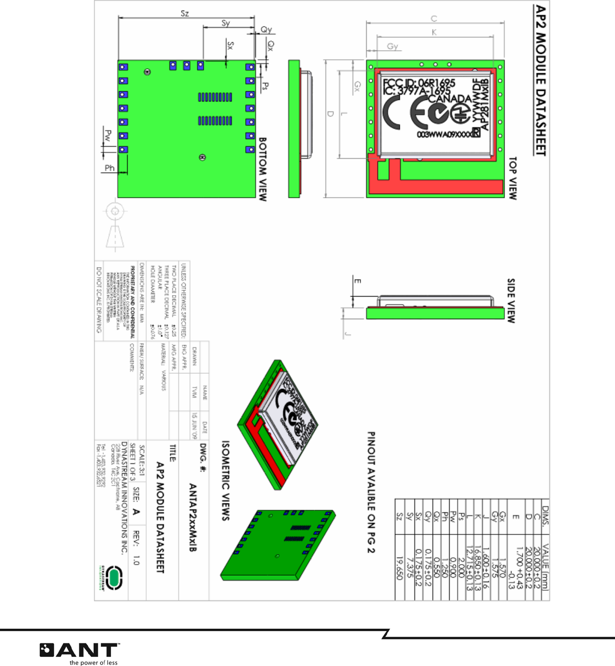
4 Mechanical Drawings
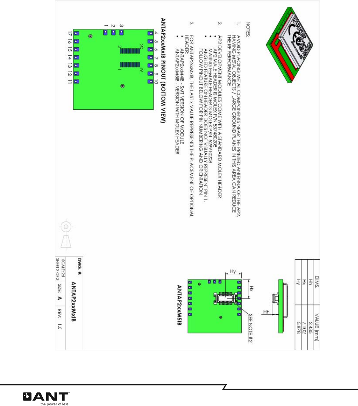
AP2 RF Transceiver Module 17 of 19
228 River Avenue, Cochrane, Alberta, Canada T4C 2C1 thisisant.com
18 of 19 AP2 RF Transceiver Module
228 River Avenue, Cochrane, Alberta, Canada T4C 2C1 thisisant.com

AP2 RF Transceiver Module 19 of 19
228 River Avenue, Cochrane, Alberta, Canada T4C 2C1 thisisant.com
5 Technical Support
The AP2 module takes the reference design of nRF24AP2 from Nordic Semiconductor. Users can seek
technical support, esp. about hardware, from Nordic Semiconductor, www.nordicsemi.no. Users can also
seek application support from Dynastream Innovations, www.thisisant.com.
5.1 ANT Forum
Users are encouraged to participate to the ANT forum moderated by the application engineering team of
Dynastream Innovations for any engineering discussions. Join the ANT forum is free and open. To access
ANT forum, click www.thisisant.com/antforum
5.2 Public Technical References
Documents:
1. nRF24AP2 Product Specification, Nordic semiconductor
2. ANT Message Protocol and Usage, Dynastream Innovations
3. Interfacing with ANT General Purpose Chipsets and Modules, Dynastream Innovations
Software:
4. ANT DLL
The above documents and software are available on www.thisisant.com or www.nordicsemi.no
5.3 ANT Developer’s Zone
ANT development software, Application notes, reference designs and source codes are found in the ANT
developer’s zone. http://www.thisisant.com/pages/support/developer-zone
ANT developer’s zone is accessible to registered owners of ANT development kit.