Gemalto M2M ALS3-USR4 GSM, WCDMA, LTE Module User Manual hid als3 us
Gemalto M2M GmbH GSM, WCDMA, LTE Module hid als3 us
User Manual
M2M.GEMALTO.COM
Cinterion® ALS3-US R4
Hardware Interface Overview
Version: 03.915
DocId: ALS3-USR4_HIO_v03.915

GENERAL NOTE
THE USE OF THE PRODUCT INCLUDING THE SOFTWARE AND DOCUMENTATION (THE "PROD-
UCT") IS SUBJECT TO THE RELEASE NOTE PROVIDED TOGETHER WITH PRODUCT. IN ANY
EVENT THE PROVISIONS OF THE RELEASE NOTE SHALL PREVAIL. THIS DOCUMENT CONTAINS
INFORMATION ON GEMALTO M2M PRODUCTS. THE SPECIFICATIONS IN THIS DOCUMENT ARE
SUBJECT TO CHANGE AT GEMALTO M2M'S DISCRETION. GEMALTO M2M GMBH GRANTS A NON-
EXCLUSIVE RIGHT TO USE THE PRODUCT. THE RECIPIENT SHALL NOT TRANSFER, COPY,
MODIFY, TRANSLATE, REVERSE ENGINEER, CREATE DERIVATIVE WORKS; DISASSEMBLE OR
DECOMPILE THE PRODUCT OR OTHERWISE USE THE PRODUCT EXCEPT AS SPECIFICALLY
AUTHORIZED. THE PRODUCT AND THIS DOCUMENT ARE PROVIDED ON AN "AS IS" BASIS ONLY
AND MAY CONTAIN DEFICIENCIES OR INADEQUACIES. TO THE MAXIMUM EXTENT PERMITTED
BY APPLICABLE LAW, GEMALTO M2M GMBH DISCLAIMS ALL WARRANTIES AND LIABILITIES.
THE RECIPIENT UNDERTAKES FOR AN UNLIMITED PERIOD OF TIME TO OBSERVE SECRECY
REGARDING ANY INFORMATION AND DATA PROVIDED TO HIM IN THE CONTEXT OF THE DELIV-
ERY OF THE PRODUCT. THIS GENERAL NOTE SHALL BE GOVERNED AND CONSTRUED
ACCORDING TO GERMAN LAW.
Copyright
Transmittal, reproduction, dissemination and/or editing of this document as well as utilization of its con-
tents and communication thereof to others without express authorization are prohibited. Offenders will be
held liable for payment of damages. All rights created by patent grant or registration of a utility model or
design patent are reserved.
Copyright © 2017, Gemalto M2M GmbH, a Gemalto Company
Trademark Notice
Gemalto, the Gemalto logo, are trademarks and service marks of Gemalto and are registered in certain
countries. Microsoft and Windows are either registered trademarks or trademarks of Microsoft Corpora-
tion in the United States and/or other countries. All other registered trademarks or trademarks mentioned
in this document are property of their respective owners.
ALS3-USR4_HIO_v03.915 2017-03-27
Confidential / Preliminary
Cinterion® ALS3-US R4 Hardware Interface Overview
2
Page 2 of 44
Document Name: Cinterion® ALS3-US R4 Hardware Interface Overview
Version: 03.915
Date: 2017-03-27
DocId: ALS3-USR4_HIO_v03.915
Status Confidential / Preliminary

Cinterion® ALS3-US R4 Hardware Interface Overview
Contents
44
ALS3-USR4_HIO_v03.915 2017-03-27
Confidential / Preliminary
Page 3 of 44
Contents
0 Document History ....................................................................................................... 6
1 Introduction ................................................................................................................. 7
1.1 Supported Products ........................................................................................... 7
1.2 Related Documents ........................................................................................... 7
1.3 Terms and Abbreviations................................................................................... 7
1.4 Regulatory and Type Approval Information ..................................................... 10
1.4.1 Directives and Standards.................................................................... 10
1.4.2 SAR requirements specific to portable mobiles .................................. 13
1.4.3 SELV Requirements ........................................................................... 14
1.4.4 Safety Precautions.............................................................................. 14
2 Product Concept ....................................................................................................... 15
2.1 Key Features at a Glance ................................................................................ 15
2.2 ALS3-US R4 System Overview ....................................................................... 18
3 Application Interface................................................................................................. 19
3.1 Operating Modes ............................................................................................. 20
3.2 Power Supply................................................................................................... 21
3.3 USB Interface................................................................................................... 22
3.4 Serial Interface ASC0 ...................................................................................... 23
3.5 UICC/SIM/USIM Interface................................................................................ 24
3.6 Analog Audio Interface..................................................................................... 26
3.7 Digital Audio Interface...................................................................................... 26
3.8 Analog-to-Digital Converter (ADC)................................................................... 26
3.9 GPIO Interface................................................................................................. 26
4 GNSS Receiver.......................................................................................................... 27
5 Antenna Interfaces.................................................................................................... 28
5.1 GSM/UMTS/LTE Antenna Interface................................................................. 28
5.1.1 Antenna Installation ............................................................................ 29
5.1.2 RF Line Routing Design...................................................................... 30
5.1.2.1 Line Arrangement Examples ............................................... 30
5.1.2.2 Routing Example................................................................. 32
5.2 GNSS Antenna Interface ................................................................................. 33
6 Mechanics.................................................................................................................. 35
6.1 Mechanical Dimensions of ALS3-US R4 ......................................................... 35
7 Sample Application................................................................................................... 37
8 Reference Approval .................................................................................................. 39
8.1 Reference Equipment for Type Approval......................................................... 39
8.2 Compliance with FCC and IC Rules and Regulations ..................................... 40
9 Appendix.................................................................................................................... 42
9.1 List of Parts and Accessories........................................................................... 42

Cinterion® ALS3-US R4 Hardware Interface Overview
Tables
44
ALS3-USR4_HIO_v03.915 2017-03-27
Confidential / Preliminary
Page 4 of 44
Tables
Table 1: Directives ....................................................................................................... 10
Table 2: Standards of North American type approval .................................................. 10
Table 3: Standards of European type approval............................................................ 10
Table 4: Requirements of quality ................................................................................. 11
Table 5: Standards of the Ministry of Information Industry of the
People’s Republic of China............................................................................ 12
Table 6: Toxic or hazardous substances or elements with defined concentration
limits............................................................................................................... 12
Table 7: Overview of operating modes ........................................................................ 20
Table 8: Signals of the SIM interface (SMT application interface) ............................... 24
Table 9: Return loss in the active band........................................................................ 28
Table 10: Antenna gain limits for FCC and IC................................................................ 40
Table 11: List of parts and accessories.......................................................................... 42
Table 12: Molex sales contacts (subject to change) ...................................................... 43
Table 13: Hirose sales contacts (subject to change) ..................................................... 43

Cinterion® ALS3-US R4 Hardware Interface Overview
Figures
44
ALS3-USR4_HIO_v03.915 2017-03-27
Confidential / Preliminary
Page 5 of 44
Figures
Figure 1: ALS3-US R4 system overview....................................................................... 18
Figure 2: Decoupling capacitor(s) for BATT+................................................................ 21
Figure 3: USB circuit ..................................................................................................... 22
Figure 4: Serial interface ASC0..................................................................................... 23
Figure 5: First UICC/SIM/USIM interface ...................................................................... 25
Figure 6: Second UICC/SIM/USIM interface................................................................. 25
Figure 7: Embedded Stripline line arrangement............................................................ 30
Figure 8: Micro-Stripline line arrangement samples...................................................... 31
Figure 9: Routing to application‘s RF connector ........................................................... 32
Figure 10: ALS3-US R4 evaluation board layer table ..................................................... 32
Figure 11: Supply voltage for active GNSS antenna....................................................... 33
Figure 12: ESD protection for passive GNSS antenna ................................................... 34
Figure 13: ALS3-US R4 – top and bottom view .............................................................. 35
Figure 14: Dimensions of ALS3-US R4 (all dimensions in mm)...................................... 36
Figure 15: ALS3-US R4 sample application.................................................................... 38
Figure 16: Reference equipment for type approval......................................................... 39

Cinterion® ALS3-US R4 Hardware Interface Overview
1 Introduction
14
ALS3-USR4_HIO_v03.915 2017-03-27
Confidential / Preliminary
Page 7 of 44
1 Introduction
The document1 describes the hardware of the Cinterion® ALS3-US R4 module, designed to
connect to a cellular device application and the air interface. It helps you quickly retrieve inter-
face specifications, electrical and mechanical details and information on the requirements to be
considered for integrating further components.
1.1 Supported Products
This document applies to the following Gemalto M2M products:
•Cinterion
® ALS3-US R4 module
1.2 Related Documents
[1] AT Command Set for your Gemalto M2M product
[2] Release Notes for your Gemalto M2M product
[3] Application Note 48: SMT Module Integration
[4] Universal Serial Bus Specification Revision 2.0, April 27, 2000
1.3 Terms and Abbreviations
1. The document is effective only if listed in the appropriate Release Notes as part of the technical docu-
mentation delivered with your Gemalto M2M product.
Abbreviation Description
AMR Adaptive Multirate
ANSI American National Standards Institute
ARP Antenna Reference Point
BIP Bearer Independent Protocol
CE Conformité Européene (European Conformity)
CS Coding Scheme
CS Circuit Switched
CSD Circuit Switched Data
CSFB Circuit Switched Fallback
DCS Digital Cellular System
DL Download
dnu Do not use
DRX Discontinuous Reception
DSB Development Support Board

Cinterion® ALS3-US R4 Hardware Interface Overview
1.3 Terms and Abbreviations
14
ALS3-USR4_HIO_v03.915 2017-03-27
Confidential / Preliminary
Page 8 of 44
DTX Discontinuous Transmission
EDGE Enhanced Data rates for GSM Evolution
EFR Enhanced Full Rate
EGSM Extended GSM
EMC Electromagnetic Compatibility
ESD Electrostatic Discharge
ETS European Telecommunication Standard
ETSI European Telecommunications Standards Institute
FCC Federal Communications Commission (U.S.)
FDD Frequency Division Duplex
FR Full Rate
GPRS General Packet Radio Service
GSM Global Standard for Mobile Communications
HiZ High Impedance
HR Half Rate
HSDPA High Speed Downlink Packet Access
I/O Input/Output
IMEI International Mobile Equipment Identity
ISO International Standards Organization
ITU International Telecommunications Union
kbps kbits per second
LED Light Emitting Diode
LGA Land Grid Array
LTE Long term evolution
MBB Moisture barrier bag
Mbps Mbits per second
MCS Modulation and Coding Scheme
MIMO Multiple Input Multiple Output
MLCC Multi Layer Ceramic Capacitor
MO Mobile Originated
MS Mobile Station, also referred to as TE
MSL Moisture Sensitivity Level
MT Mobile Terminated
nc Not connected
NTC Negative Temperature Coefficient
PCB Printed Circuit Board
Abbreviation Description

Cinterion® ALS3-US R4 Hardware Interface Overview
1.3 Terms and Abbreviations
14
ALS3-USR4_HIO_v03.915 2017-03-27
Confidential / Preliminary
Page 9 of 44
PCL Power Control Level
PCS Personal Communication System, also referred to as GSM 1900
PD Pull Down resistor
PDU Protocol Data Unit
PS Packet Switched
PSK Phase Shift Keying
PU Pull Up resistor
QAM Quadrature Amplitude Modulation
R&TTE Radio and Telecommunication Terminal Equipment
RF Radio Frequency
rfu Reserved for future use
ROPR Radio Output Power Reduction
RTC Real Time Clock
Rx Receive Direction
SAR Specific Absorption Rate
SELV Safety Extra Low Voltage
SIM Subscriber Identification Module
SMD Surface Mount Device
SMS Short Message Service
SMT Surface Mount Technology
SRAM Static Random Access Memory
SRB Signaling Radio Bearer
TE Terminal Equipment
TPC Transmit Power Control
TS Technical Specification
Tx Transmit Direction
UL Upload
UMTS Universal Mobile Telecommunications System
URC Unsolicited Result Code
USB Universal Serial Bus
UICC USIM Integrated Circuit Card
USIM UMTS Subscriber Identification Module
USAT U/SIM Application Toolkit
WB-AMR Wideband Adaptive Multirate
WCDMA Wideband Code Division Multiple Access
Abbreviation Description
Cinterion® ALS3-US R4 Hardware Interface Overview
1.4 Regulatory and Type Approval Information
14
ALS3-USR4_HIO_v03.915 2017-03-27
Confidential / Preliminary
Page 10 of 44
1.4 Regulatory and Type Approval Information
1.4.1 Directives and Standards
ALS3-US R4 has been designed to comply with the directives and standards listed below.
It is the responsibility of the application manufacturer to ensure compliance of the final product
with all provisions of the applicable directives and standards as well as with the technical spec-
ifications provided in the "ALS3-US R4 Hardware Interface Description".1
1. Manufacturers of applications which can be used in the US shall ensure that their applications have a
PTCRB approval. For this purpose they can refer to the PTCRB approval of the respective module.
Table 1: Directives
99/05/EC Directive of the European Parliament and of the council of 9 March 1999 on
radio equipment and telecommunications terminal equipment and the
mutual recognition of their conformity (in short referred to as R&TTE Direc-
tive 1999/5/EC).
The product is labeled with the CE conformity mark
2014/53/EU Directive of the European Parliament and of the council of 16 April 2014 on
the harmonization of the laws of the Member States relating to the making
available on the market of radio equipment and repealing Directive 1999/
05/EC.
2002/95/EC (RoHS 1)
2011/65/EC (RoHS 2) Directive of the European Parliament and of the Council of
27 January 2003 (and revised on 8 June 2011) on the
restriction of the use of certain hazardous substances in
electrical and electronic equipment (RoHS)
Table 2: Standards of North American type approval
CFR Title 47 Code of Federal Regulations, Part 22, Part 24 and Part 27; US Equipment
Authorization FCC
OET Bulletin 65
(Edition 97-01) Evaluating Compliance with FCC Guidelines for Human Exposure to
Radiofrequency Electromagnetic Fields
UL 60 950-1 Product Safety Certification (Safety requirements)
NAPRD.03 V5.30 Overview of PCS Type certification review board Mobile Equipment Type
Certification and IMEI control
PCS Type Certification Review board (PTCRB)
RSS130, RSS132,
RSS133, RSS139 Canadian Standard
Table 3: Standards of European type approval
3GPP TS 51.010-1 Digital cellular telecommunications system (Release 7); Mobile Station
(MS) conformance specification;
ETSI EN 301 511
V12.1.1 Global System for Mobile communications (GSM); Harmonized standard for
mobile stations in the GSM 900 and DCS 1800 bands covering essential
requirements under article 3.2 of the R&TTE directive (1999/5/EC)
GCF-CC V3.64 Global Certification Forum - Certification Criteria
Cinterion® ALS3-US R4 Hardware Interface Overview
1.4 Regulatory and Type Approval Information
14
ALS3-USR4_HIO_v03.915 2017-03-27
Confidential / Preliminary
Page 11 of 44
ETSI EN 301 489-01
V1.9.2 Electromagnetic Compatibility and Radio spectrum Matters (ERM); Electro-
magnetic Compatibility (EMC) standard for radio equipment and services;
Part 1: Common Technical Requirements
ETSI EN 301 489-03
V1.6.1 Electromagnetic Compatibility and Radio spectrum Matters (ERM); Electro-
magnetic Compatibility (EMC) standard for radio equipment and services;
Part 1: Specific requirements for Short-Range Devices (SRD) operating on
frequencies between 9 kHz and 25 GHz
ETSI EN 301 489-07
V1.3.1 Electromagnetic Compatibility and Radio spectrum Matters (ERM); Electro-
magnetic Compatibility (EMC) standard for radio equipment and services;
Part 7: Specific conditions for mobile and portable radio and ancillary equip-
ment of digital cellular radio telecommunications systems (GSM and DCS)
EN 300 440-02 V1.4.1 Electromagnetic compatibility and Radio spectrum Matters (ERM); Short
range devices; Radio equipment to be used in the 1 GHz to 40 GHz fre-
quency range; Part 2: Harmonized EN covering essential requirements of
article 3.2 of the R&TTE Directive
EN 62311:2008 Assessment of electronic and electrical equipment related to human expo-
sure restrictions for electromagnetic fields (0 Hz - 300 GHz)
IEC/EN 60950-1:2006+
A11:2009+A1:2010+
A12:2011+A2:2013
Safety of information technology equipment
Table 4: Requirements of quality
IEC 60068 Environmental testing
DIN EN 60529 IP codes
Table 3: Standards of European type approval
Cinterion® ALS3-US R4 Hardware Interface Overview
1.4 Regulatory and Type Approval Information
14
ALS3-USR4_HIO_v03.915 2017-03-27
Confidential / Preliminary
Page 12 of 44
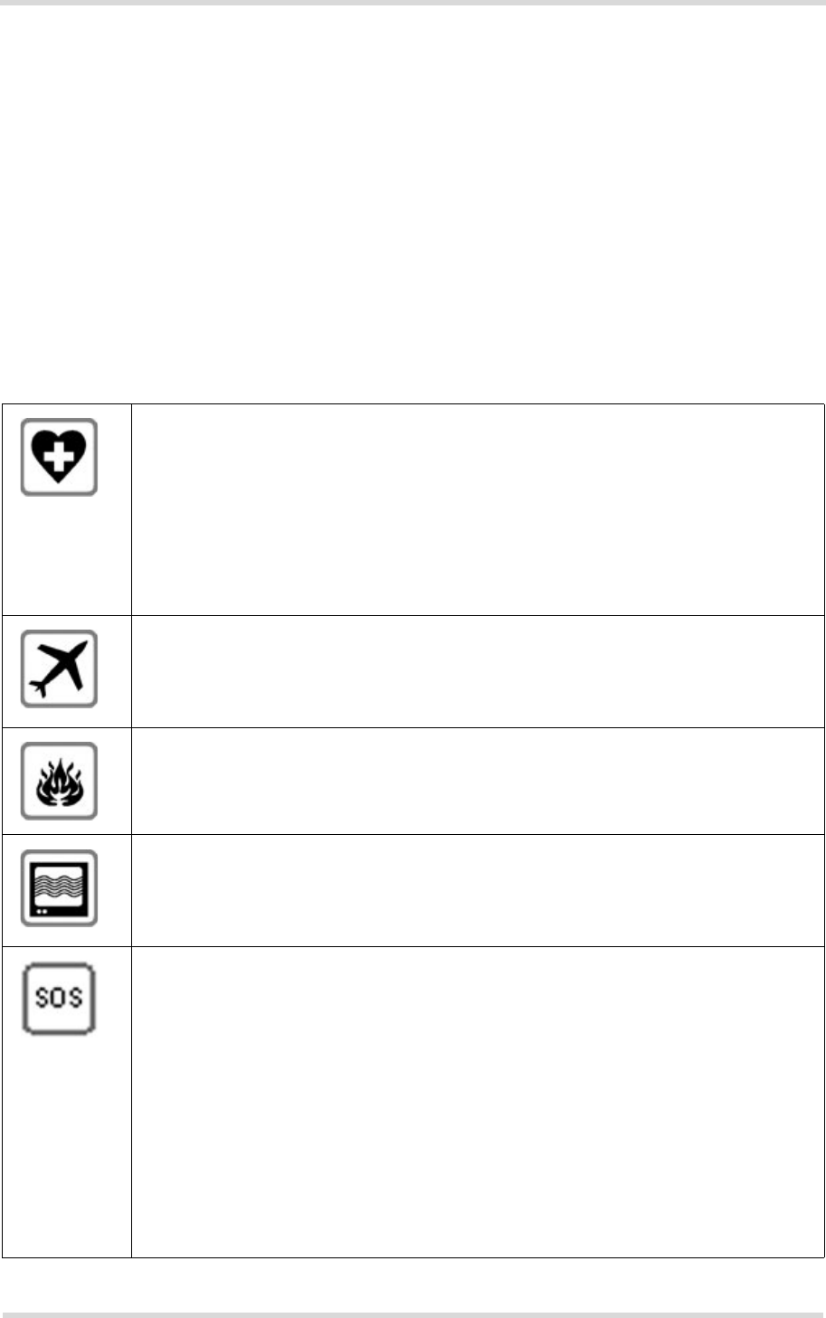
Table 6: Toxic or hazardous substances or elements with defined concentration limits
Table 5: Standards of the Ministry of Information Industry of the People’s Republic of China
SJ/T 11363-2006 “Requirements for Concentration Limits for Certain Hazardous Substances
in Electronic Information Products” (2006-06).
SJ/T 11364-2006 “Marking for Control of Pollution Caused by Electronic
Information Products” (2006-06).
According to the “Chinese Administration on the Control of
Pollution caused by Electronic Information Products”
(ACPEIP) the EPUP, i.e., Environmental Protection Use
Period, of this product is 20 years as per the symbol
shown here, unless otherwise marked. The EPUP is valid only as long as
the product is operated within the operating limits described in the Hardware
Interface Description.
Please see Table 6 for an overview of toxic or hazardous substances or ele-
ments that might be contained in product parts in concentrations above the
limits defined by SJ/T 11363-2006.

Cinterion® ALS3-US R4 Hardware Interface Overview
1.4 Regulatory and Type Approval Information
14
ALS3-USR4_HIO_v03.915 2017-03-27
Confidential / Preliminary
Page 13 of 44
1.4.2 SAR requirements specific to portable mobiles
Mobile phones, PDAs or other portable transmitters and receivers incorporating a GSM/UMTS/
LTE module must be in accordance with the guidelines for human exposure to radio frequency
energy. This requires the Specific Absorption Rate (SAR) of portable ALS3-US R4 based ap-
plications to be evaluated and approved for compliance with national and/or international reg-
ulations.
Since the SAR value varies significantly with the individual product design manufacturers are
advised to submit their product for approval if designed for portable use. For US markets the
relevant directives are mentioned below. It is the responsibility of the manufacturer of the final
product to verify whether or not further standards, recommendations or directives are in force
outside these areas.
Products intended for sale on US markets
ES 59005/ANSI C95.1 Considerations for evaluation of human exposure to electromagnetic
fields (EMFs) from mobile telecommunication equipment (MTE) in the
frequency range 30MHz - 6GHz
IMPORTANT:
Manufacturers of portable applications based on ALS3-US R4 modules are required to have
their final product certified and apply for their own FCC Grant and Industry Canada Certificate
related to the specific portable mobile.
Cinterion® ALS3-US R4 Hardware Interface Overview
1.4 Regulatory and Type Approval Information
14
ALS3-USR4_HIO_v03.915 2017-03-27
Confidential / Preliminary
Page 14 of 44
1.4.3 SELV Requirements
The power supply connected to the ALS3-US R4 module shall be in compliance with the SELV
requirements defined in EN 60950-1.
1.4.4 Safety Precautions
The following safety precautions must be observed during all phases of the operation, usage,
service or repair of any cellular terminal or mobile incorporating ALS3-US R4. Manufacturers
of the cellular terminal are advised to convey the following safety information to users and op-
erating personnel and to incorporate these guidelines into all manuals supplied with the prod-
uct. Failure to comply with these precautions violates safety standards of design, manufacture
and intended use of the product. Gemalto M2M assumes no liability for customer’s failure to
comply with these precautions.
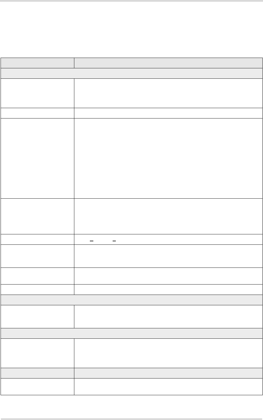
When in a hospital or other health care facility, observe the restrictions on the use of
mobiles. Switch the cellular terminal or mobile off, if instructed to do so by the guide-
lines posted in sensitive areas. Medical equipment may be sensitive to RF energy.
The operation of cardiac pacemakers, other implanted medical equipment and hearing
aids can be affected by interference from cellular terminals or mobiles placed close to
the device. If in doubt about potential danger, contact the physician or the manufac-
turer of the device to verify that the equipment is properly shielded. Pacemaker
patients are advised to keep their hand-held mobile away from the pacemaker, while
it is on.
Switch off the cellular terminal or mobile before boarding an aircraft. Make sure it can-
not be switched on inadvertently. The operation of wireless appliances in an aircraft is
forbidden to prevent interference with communications systems. Failure to observe
these instructions may lead to the suspension or denial of cellular services to the
offender, legal action, or both.
Do not operate the cellular terminal or mobile in the presence of flammable gases or
fumes. Switch off the cellular terminal when you are near petrol stations, fuel depots,
chemical plants or where blasting operations are in progress. Operation of any electri-
cal equipment in potentially explosive atmospheres can constitute a safety hazard.
Your cellular terminal or mobile receives and transmits radio frequency energy while
switched on. Remember that interference can occur if it is used close to TV sets,
radios, computers or inadequately shielded equipment. Follow any special regulations
and always switch off the cellular terminal or mobile wherever forbidden, or when you
suspect that it may cause interference or danger.
IMPORTANT!
Cellular terminals or mobiles operate using radio signals and cellular networks.
Because of this, connection cannot be guaranteed at all times under all conditions.
Therefore, you should never rely solely upon any wireless device for essential com-
munications, for example emergency calls.
Remember, in order to make or receive calls, the cellular terminal or mobile must be
switched on and in a service area with adequate cellular signal strength.
Some networks do not allow for emergency calls if certain network services or phone
features are in use (e.g. lock functions, fixed dialing etc.). You may need to deactivate
those features before you can make an emergency call.
Some networks require that a valid SIM card be properly inserted in the cellular termi-
nal or mobile.
Cinterion® ALS3-US R4 Hardware Interface Overview
2 Product Concept
18
ALS3-USR4_HIO_v03.915 2017-03-27
Confidential / Preliminary
Page 15 of 44
2 Product Concept
2.1 Key Features at a Glance
Feature Implementation
General
Frequency bands GSM/GPRS/EDGE: Quad band, 850/900/1800/1900MHz
UMTS/HSPA+: Triple band, 850 (BdV) / AWS (BdIV) / 1900MHz (BdII)
LTE: Quad band, 700 (Bd17) / 850 (Bd5) / AWS (Bd4) / 1900MHz (Bd2)
GSM class Small MS
Output power (according to
Release 99) Class 4 (+33dBm ±2dB) for EGSM850
Class 4 (+33dBm ±2dB) for EGSM900
Class 1 (+30dBm ±2dB) for GSM1800
Class 1 (+30dBm ±2dB) for GSM1900
Class E2 (+27dBm ± 3dB) for GSM 850 8-PSK
Class E2 (+27dBm ± 3dB) for GSM 900 8-PSK
Class E2 (+26dBm +3 /-4dB) for GSM 1800 8-PSK
Class E2 (+26dBm +3 /-4dB) for GSM 1900 8-PSK
Class 3 (+24dBm +1/-3dB) for UMTS 1900,WCDMA FDD BdII
Class 3 (+24dBm +1/-3dB) for UMTS AWS, WCDMA FDD BdIV
Class 3 (+24dBm +1/-3dB) for UMTS 850, WCDMA FDD BdV
Output power (according to
Release 8) Class 3 (+23dBm +-2dB) for LTE 1900, LTE FDD Bd2
Class 3 (+23dBm +-2dB) for LTE AWS, LTE FDD Bd4
Class 3 (+23dBm +-2dB) for LTE 850, LTE FDD Bd5
Class 3 (+23dBm +-2dB) for LTE 700, LTE FDD Bd17
Power supply 3.3V < VBATT+ < 4.2V
Operating temperature
(board temperature) Normal operation: -30°C to +85°C
Restricted operation: -40°C to +95°C
Physical Dimensions: 33mm x 29mm x 2.2mm
Weight: approx. 4.5g
RoHS All hardware components fully compliant with EU RoHS Directive
LTE features
3GPP Release 9 UE CAT 3 supported
DL 100Mbps, UL 50Mbps
2x2 MIMO in DL direction
HSPA features
3GPP Release 8 UE CAT. 14, 24
DC-HSPA+ – DL 42Mbps
HSUPA – UL 5.76Mbps
Compressed mode (CM) supported according to 3GPP TS25.212
UMTS features
3GPP Release 8 PS data rate – 384 kbps DL / 384 kbps UL
Cinterion® ALS3-US R4 Hardware Interface Overview
2.1 Key Features at a Glance
18
ALS3-USR4_HIO_v03.915 2017-03-27
Confidential / Preliminary
Page 16 of 44
GSM / GPRS / EGPRS features
Data transfer GPRS:
• Multislot Class 12
• Mobile Station Class B
• Coding Scheme 1 – 4
EGPRS:
• Multislot Class 12
• EDGE E2 power class for 8 PSK
• Downlink coding schemes – CS 1-4, MCS 1-9
• Uplink coding schemes – CS 1-4, MCS 1-9
• SRB loopback and test mode B
• 8-bit, 11-bit RACH
• 1 phase/2 phase access procedures
• Link adaptation and IR
• NACC, extended UL TBF
• Mobile Station Class B
SMS Point-to-point MT and MO
Cell broadcast
Text and PDU mode
Software
AT commands Hayes, 3GPP TS 27.007 and 27.005, and proprietary Gemalto M2M com-
mands
Firmware update Generic update from host application over USB and ASC0
U/SIM application toolkit USAT letter c; with BIP
Audio Audio speech codecs
GSM: WB-AMR, AMR, EFR, FR, HR
3GPP: WB-AMR, AMR
Speakerphone operation, echo cancellation, noise suppression, 9 ringing
tones
VoLTE support for multiple operators, with CSFB
GNSS Features
Protocol NMEA (for GPS, GLONASS and Galileo related sentences)
Modes Standalone GNSS
Assisted GNSS
- Control plane - E911
- User plane - gpsOneXTRA™
General Power saving modes
Power supply for active antenna
Interfaces
Module interface Surface mount device with solderable connection pads (SMT application
interface).
Land grid array (LGA) technology ensures high solder joint reliability and
provides the possibility to use an optional module mounting socket.
For more information on how to integrate SMT modules see also [3]. This
application note comprises chapters on module mounting and application
layout issues as well as on additional SMT application development
equipment.
Feature Implementation

Cinterion® ALS3-US R4 Hardware Interface Overview
2.1 Key Features at a Glance
18
ALS3-USR4_HIO_v03.915 2017-03-27
Confidential / Preliminary
Page 17 of 44
Antenna 50. GSM/UMTS/LTE main antenna, UMTS/LTE Diversity/MIMO
antenna, (active/passive) GNSS antenna
USB USB 2.0 High Speed (480Mbit/s) device interface
Serial interface ASC0:
• 8-wire modem interface with status and control lines, unbalanced,
asynchronous
• Adjustable baud rates: 115,200bps to 921,600bps
• Supports RTS0/CTS0 hardware flow control
UICC interface 2 UICC interfaces (switchable)
Supported chip cards: UICC/SIM/USIM 3V, 1.8V
Audio 1 digital interface (PCM or I2S)
1 analog interface with microphone feeding
Status Signal line to indicate network connectivity state
RING0 Signal line to indicate incoming calls and other types of URCs
Power on/off, Reset
Power on/off Switch-on by hardware signal IGT
Switch-off by AT command (AT^SMSO) or IGT
Automatic switch-off in case of critical temperature or voltage conditions
Reset Orderly shutdown and reset by AT command
Emergency-off Emergency-off by hardware signal EMERG_OFF if IGT is not active
Special Features
Antenna SAIC (Single Antenna Interference Cancellation) / DARP (Downlink
Advanced Receiver Performance)
Rx Diversity (receiver type 3i - 64-QAM) / MIMO
GPIO 10 I/O pins of the application interface programmable as GPIO.
GPIOs can be configured as low current indicator (LCI).
GPIOs can be configured for antenna diagnosis.
GPIO1 can be configured as dead reckoning synchronization signal.
GPIO2 can be configured as 700MHz antenna switch control signal.
GPIOs can be configured as remote host wakeup lines.
Programming is done via AT commands.
ADC inputs Analog-to-Digital Converter with three unbalanced analog inputs for
(external) antenna diagnosis.
Evaluation kit
Evaluation module ALS3-US R4 module soldered onto a dedicated PCB that can be con-
nected to an adapter in order to be mounted onto the DSB75.
DSB75 DSB75 Development Support Board designed to test and type approve
Gemalto M2M modules and provide a sample configuration for applica-
tion engineering. A special adapter is required to connect the ALS3-US
R4 evaluation module to the DSB75.
Feature Implementation
Cinterion® ALS3-US R4 Hardware Interface Overview
2.2 ALS3-US R4 System Overview
18
ALS3-USR4_HIO_v03.915 2017-03-27
Confidential / Preliminary
Page 18 of 44
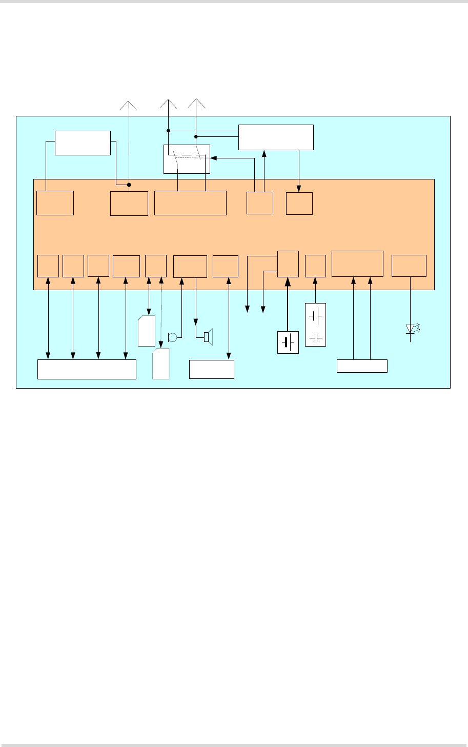
2.2 ALS3-US R4 System Overview
Figure 1: ALS3-US R4 system overview
USB Serial
ASC0 UICC Power
supply IGT,
Emergency Off
SIM
card
Host application On/Off
Module
Application
GSM/UMTS/LTE
Antenna diversity
Power for application
(VEXT)
Power indication
(PWR_IND)
Modem interface
Digital
audio
PCM or I2S
codec
GSM/UMTS/LTE
12
GNSS
GNSS antenna
GPIO
2x
GPIO
Antenna
diagnostic
2x
ADC
Antenna
switch
Power
supply
GNSS active
antenna supply,
current limiter
ADC Net state/
status
Analog
audio
SIM
card
RTC
or

Cinterion® ALS3-US R4 Hardware Interface Overview
3 Application Interface
27
ALS3-USR4_HIO_v03.915 2017-03-27
Confidential / Preliminary
Page 19 of 44
3 Application Interface
ALS3-US R4 is equipped with an SMT application interface (LGA pads) that connects to the
external application. The host interface incorporates several sub-interfaces described in the fol-
lowing sections:
• Operating modes - see Section 3.1
• Power supply - see Section 3.2
• Serial interface USB - see Section 3.3
• Serial interface ASC0 - Section 3.4
• UICC/SIM/USIM interface - see Section 3.5
• Analog audio interface - see Section 3.6
• Digital audio interface (PCM or I2S) - see Section 3.7
• ADC interface - Section 3.8
• GPIO interface - Section 3.9
Cinterion® ALS3-US R4 Hardware Interface Overview
3.1 Operating Modes
27
ALS3-USR4_HIO_v03.915 2017-03-27
Confidential / Preliminary
Page 20 of 44
3.1 Operating Modes
The table below briefly summarizes the various operating modes referred to in the following
chapters.
Table 7: Overview of operating modes
Mode Function
Normal
operation GSM / GPRS /
UMTS / HSPA /
LTE SLEEP
Power saving set automatically when no call is in progress and the USB
connection is detached and no active communication via ASC0. Also,
the GNSS active antenna mode has to be turned off or set to "auto".
GSM / GPRS /
UMTS / HSPA /
LTE IDLE
Power saving disabled or an USB connection active, but no data trans-
fer in progress.
GPRS DATA GPRS data transfer in progress. Power consumption depends on net-
work settings (e.g. power control level), uplink / downlink data rates and
GPRS configuration (e.g. used multislot settings).
EGPRS DATA EGPRS data transfer in progress. Power consumption depends on net-
work settings (e.g. power control level), uplink / downlink data rates and
EGPRS configuration (e.g. used multislot settings).
UMTS DATA UMTS data transfer in progress. Power consumption depends on net-
work settings (e.g. TPC Pattern) and data transfer rate.
HSPA DATA HSPA data transfer in progress. Power consumption depends on net-
work settings (e.g. TPC Pattern) and data transfer rate.
LTE DATA LTE data transfer in progress. Power consumption depends on network
settings (e.g. TPC Pattern) and data transfer rate.
Power
Down Normal shutdown after sending the AT^SMSO command. Only a voltage regulator is active
for powering the RTC. Software is not active. Interfaces are not accessible. Operating volt-
age (connected to BATT+) remains applied.
Airplane
mode Airplane mode shuts down the radio part of the module, causes the module to log off from
the GSM/GPRS network and disables all AT commands whose execution requires a radio
connection.
Airplane mode can be controlled by AT command (see [1]).
Cinterion® ALS3-US R4 Hardware Interface Overview
3.2 Power Supply
27
ALS3-USR4_HIO_v03.915 2017-03-27
Confidential / Preliminary
Page 21 of 44
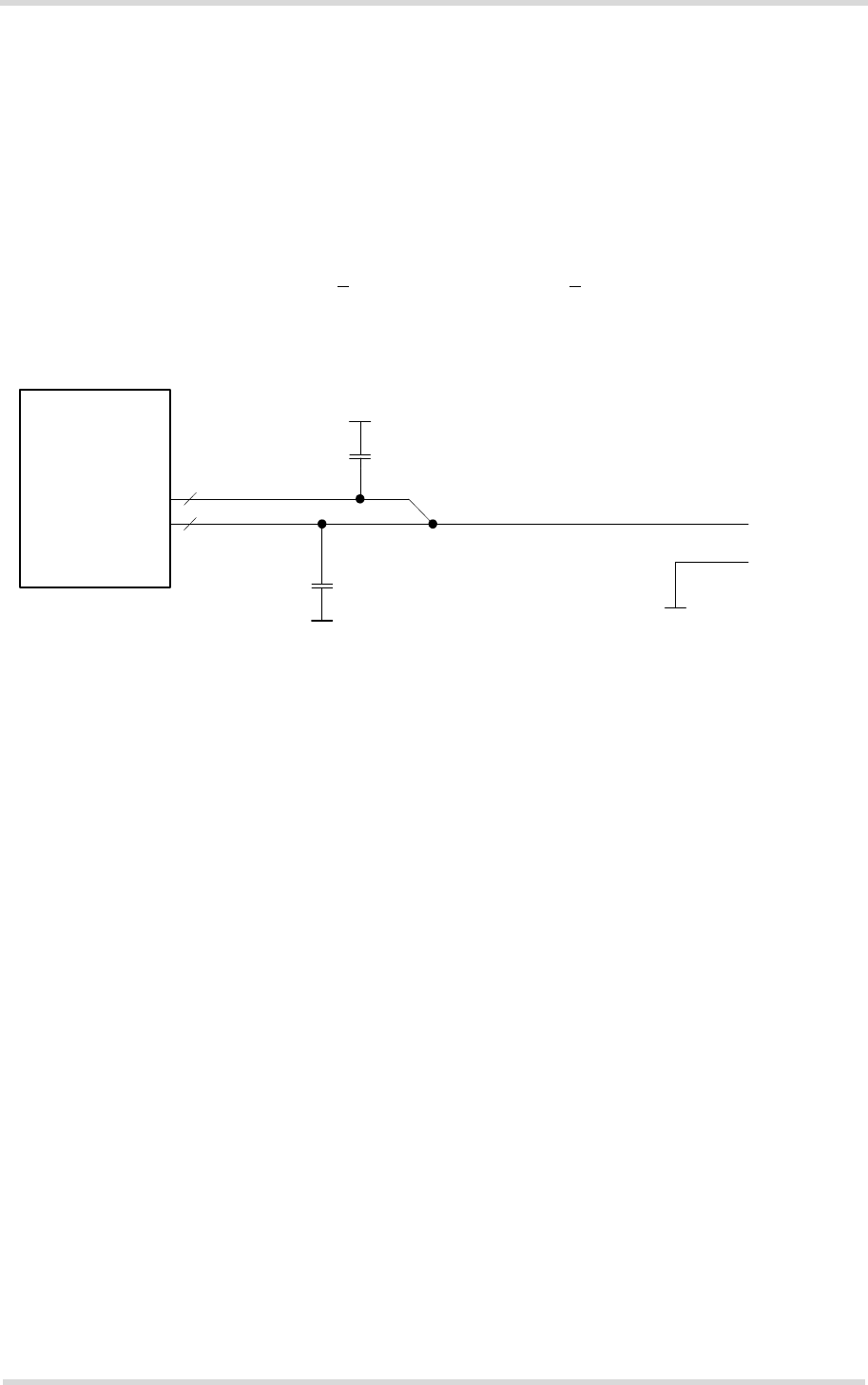
3.2 Power Supply
ALS3-US R4 needs to be connected to a power supply at the SMT application interface - 4 lines
BATT+, and GND. There are two separate voltage domains for BATT+:
• BATT+_RF with 2 lines for the RF power amplifier supply
• BATT+ with 2 lines for the general power management.
The main power supply from an external application has to be a single voltage source and has
to be expanded to two sub paths (star structure). Each voltage domain must be decoupled by
application with low ESR capacitors (> 47µF MLCC @ BATT+; > 4x47µF MLCC @ BATT+_RF)
as close as possible to LGA pads. Figure 2 shows a sample circuit for decoupling capacitors
for BATT+.
Figure 2: Decoupling capacitor(s) for BATT+
The power supply of ALS3-US R4 must be able to provide the peak current during the uplink
transmission.
All key functions for supplying power to the device are handled by the power management IC.
It provides the following features:
• Stabilizes the supply voltages for the baseband using switching regulators and low drop lin-
ear voltage regulators.
• Switches the module's power voltages for the power-up and -down procedures.
• Delivers, across the VEXT line, a regulated voltage for an external application.
• LDO to provide SIM power supply.
BATT+
2
2
Decoupling capacitors
e.g. 47µF X5R MLCC
4x
GND
BATT+
BATT+_RF
Module
SMT interface 1x
Cinterion® ALS3-US R4 Hardware Interface Overview
3.3 USB Interface
27
ALS3-USR4_HIO_v03.915 2017-03-27
Confidential / Preliminary
Page 22 of 44
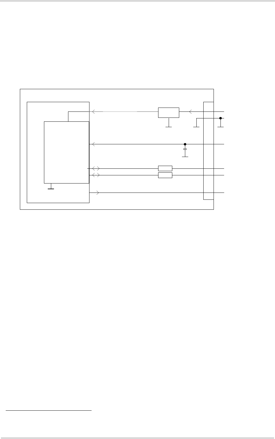
3.3 USB Interface
ALS3-US R4 supports a USB 2.0 High Speed (480Mbps) device interface. The USB interface
is primarily intended for use as command and data interface and for downloading firmware.
The USB host is responsible for supplying the VUSB_IN line. This line is for voltage detection
only. The USB part (driver and transceiver) is supplied by means of BATT+. This is because
ALS3-US R4 is designed as a self-powered device compliant with the “Universal Serial Bus
Specification Revision 2.0”1.
Figure 3: USB circuit
To properly connect the module's USB interface to the external application, a USB 2.0 compat-
ible connector and cable or hardware design is required. Furthermore, the USB modem driver
distributed with ALS3-US R4 needs to be installed.
1. The specification is ready for download on http://www.usb.org/developers/docs/usb20_docs/
DP
DN
VREG (3V075)
BATT+
USB_DP3)
lin. reg. GND
Module
Detection only VUSB_IN2)
USB part1)
1) All serial (including RS) and pull-up resistors for data lines are implemented.
USB_DN3)
3) If the USB interface is operated in High Speed mode (480MHz), it is recommended to take
special care routing the data lines USB_DP and USB_DN. Application layout should in this
case implement a differential impedance of 90 ohms for proper signal integrity.
RS
RS
VBUS 1µF
2) Since VUSB_IN is used for detection only it is recommended not to add any further
blocking capacitors on the VUSB_IN line.
Host wakeup RING0
SMT
Cinterion® ALS3-US R4 Hardware Interface Overview
3.4 Serial Interface ASC0
27
ALS3-USR4_HIO_v03.915 2017-03-27
Confidential / Preliminary
Page 23 of 44
3.4 Serial Interface ASC0
ALS3-US R4 offers an 8-wire unbalanced, asynchronous modem interface ASC0 conforming
to ITU-T V.24 protocol DCE signaling. The electrical characteristics do not comply with ITU-T
V.28. The significant levels are 0V (for low data bit or active state) and 1.8V (for high data bit
or inactive state).
ALS3-US R4 is designed for use as a DCE. Based on the conventions for DCE-DTE connec-
tions it communicates with the customer application (DTE) using the following signals:
• Port TXD @ application sends data to the module’s TXD0 signal line
• Port RXD @ application receives data from the module’s RXD0 signal line
Figure 4: Serial interface ASC0
Features:
• Includes the data lines TXD0 and RXD0, the status lines RTS0 and CTS0 and, in addition,
the modem control lines DTR0, DSR0, DCD0 and RING0.
• The RING0 signal serves to indicate incoming calls and other types of URCs (Unsolicited
Result Code). It can also be configured to send pulses to the host application, for example
to remotely wake up the application from power saving state. See [1] for details on how to
configure the RING0 line by AT^SCFG.
• Configured for 8 data bits, no parity and 1 stop bit.
• ASC0 can be operated at fixed bit rates from 115200bps up to 921600bps.
• Supports RTS0/CTS0 hardware flow control.
• Wake up from SLEEP mode by RTS0 activation.
Note: If the ASC0 serial interface is the application’s only interface, it is suggested to connect
test points on the USB signal lines as a potential tracing possibility.
Cinterion® ALS3-US R4 Hardware Interface Overview
3.5 UICC/SIM/USIM Interface
27
ALS3-USR4_HIO_v03.915 2017-03-27
Confidential / Preliminary
Page 24 of 44
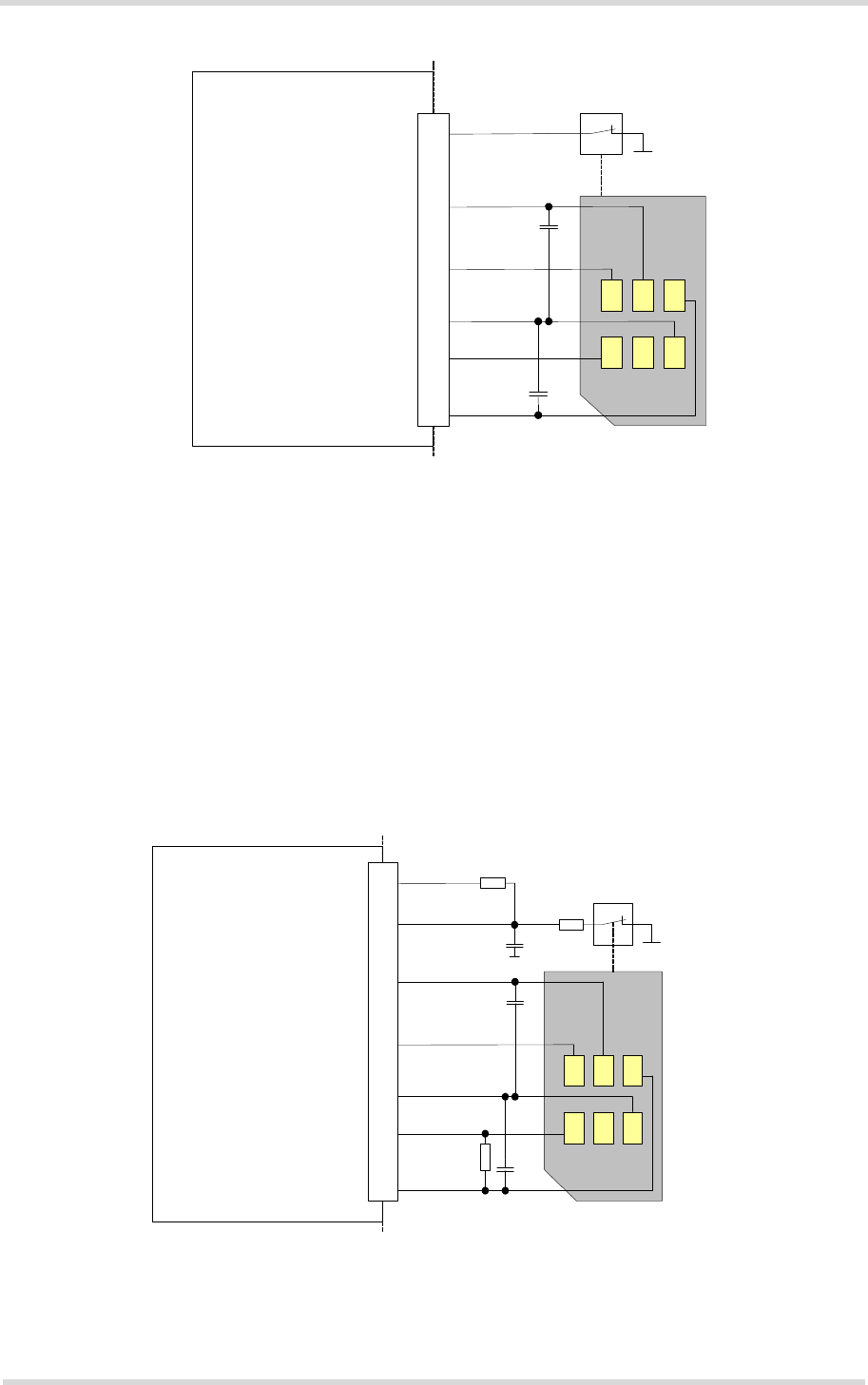
3.5 UICC/SIM/USIM Interface
ALS3-US R4 has two integrated UICC/SIM/USIM interfaces compatible with the 3GPP 31.102
and ETSI 102 221. These are wired to the host interface in order to be connected to an external
SIM card holder. Five pads on the SMT application interface are reserved for each of the SIM
two interfaces.
The UICC/SIM/USIM interfaces support 3V and 1.8V SIM cards.
The CCINx signal serves to detect whether a tray (with SIM card) is present in the card holder.
Using the CCINx signal is mandatory for compliance with the GSM 11.11 recommendation if
the mechanical design of the host application allows the user to remove the SIM card during
operation. To take advantage of this feature, an appropriate SIM card detect switch is required
on the card holder. For example, this is true for the model supplied by Molex, which has been
tested to operate with ALS3-US R4 and is part of the Gemalto M2M reference equipment sub-
mitted for type approval. See Chapter 9 for Molex ordering numbers.
Note: No guarantee can be given, nor any liability accepted, if loss of data is encountered after
removing the SIM card during operation. Also, no guarantee can be given for properly initializ-
ing any SIM card that the user inserts after having removed the SIM card during operation. In
this case, the application must restart ALS3-US R4.
Table 8: Signals of the SIM interface (SMT application interface)
Signal Description
GND Ground connection for SIM interfaces. Optionally a separate SIM ground line using e.g.,
pad N11 may be used to improve EMC.
CCCLK1
CCCLK2 Chipcard clock lines for 1st and 2nd SIM interface.
CCVCC1
CCVCC2 SIM supply voltage lines for 1st and 2nd SIM interface.
CCIO1
CCIO2 Serial data lines for 1st and 2nd SIM interface, input and output.
CCRST1
CCRST2 Chipcard reset lines for 1st and 2nd SIM interface.
CCIN1
CCIN2 Input on the baseband processor for detecting a SIM card tray in the holder. If the SIM is
removed during operation the SIM interface is shut down immediately to prevent destruc-
tion of the SIM. The CCINx signal is active low.
The CCINx signal is mandatory for applications that allow the user to remove the SIM card
during operation.
The CCINx signal is solely intended for use with a SIM card. It must not be used for any
other purposes. Failure to comply with this requirement may invalidate the type approval of
ALS3-US R4.
Cinterion® ALS3-US R4 Hardware Interface Overview
3.5 UICC/SIM/USIM Interface
27
ALS3-USR4_HIO_v03.915 2017-03-27
Confidential / Preliminary
Page 25 of 44
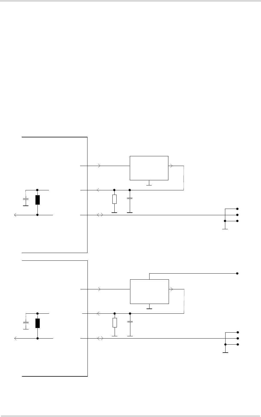
Figure 5: First UICC/SIM/USIM interface
The total cable length between the SMT application interface pads on ALS3-US R4 and the
pads of the external SIM card holder must not exceed 100mm in order to meet the specifica-
tions of 3GPP TS 51.010-1 and to satisfy the requirements of EMC compliance.
To avoid possible cross-talk from the CCCLKx signal to the CCIOx signal be careful that both
lines are not placed closely next to each other. A useful approach is using the GND line to
shield the CCIOx line from the CCCLKx line.
Note: Figure 5 shows how to connect a SIM card holder to the first SIM interface. With the sec-
ond SIM interface some internally integrated components on the SIM circuit will have to be ex-
ternally integrated as shown for the second SIM interface in Figure 6.
Figure 6: Second UICC/SIM/USIM interface
Module
open: Card removed
closed: Card inserted
CCRST1
CCVCC1
CCIO1
CCCLK1
CCIN1
SIM /
UICC
1nF
220nF
SMT application interface
GND
Module
Open: Card removed
Closed: Card inserted
CCRST2
CCVCC2
CCIO2
CCCLK2
CCIN2
SIM /
UICC
1nF
220nF
SMT application interface
GND
2k2
100pF*
VEXT 22k*
10k
* Should be placed
as close as possible
to SMT application
interface

Cinterion® ALS3-US R4 Hardware Interface Overview
3.6 Analog Audio Interface
27
ALS3-USR4_HIO_v03.915 2017-03-27
Confidential / Preliminary
Page 26 of 44
3.6 Analog Audio Interface
ALS3-US R4 has an analog audio interface with a balanced analog microphone input and a
balanced analog earpiece output. A supply voltage and an analog ground connection are pro-
vided at dedicated pads.
ALS3-US R4 offers six audio modes which can be selected with the AT^SNFS command. The
electrical characteristics of the voiceband part vary with the audio mode. For example, sending
and receiving amplification, sidetone paths, noise suppression etc. depend on the selected
mode and can be altered with AT commands (except for mode 1).
When shipped from factory, all audio parameters of ALS3-US R4 are set to audio mode 1. This
is the default configuration optimized for the Votronic HH-SI-30.3/V1.1/0 handset and used for
type approving the Gemalto M2M reference configuration.
3.7 Digital Audio Interface
ALS3-US R4 supports a digital audio interface that can be employed either as pulse code mod-
ulation interface or as inter IC sound interface. Operation of these interface variants is mutually
exclusive, and can be configured by AT command (see [1]). Default setting is pulse code mod-
ulation.
3.8 Analog-to-Digital Converter (ADC)
ALS3-US R4 provides three unbalanced ADC input lines: ADC1_IN, ADC2_IN and ADC3_IN.
They can be used to measure three independent, externally connected DC voltages in the
range of 0.3V to 3.075V.
3.9 GPIO Interface
ALS3-US R4 has 10 GPIOs for external hardware devices. Each GPIO can be configured for
use as input or output. All settings are AT command controlled.

Cinterion® ALS3-US R4 Hardware Interface Overview
4 GNSS Receiver
27
ALS3-USR4_HIO_v03.915 2017-03-27
Confidential / Preliminary
Page 27 of 44
4 GNSS Receiver
ALS3-US R4 integrates a GNSS receiver that offers the full performance of GPS/GLONASS/
Galileo technology. The GNSS receiver is able to continuously track all satellites in view, thus
providing accurate satellite position data.
The integrated GNSS receiver supports the NMEA protocol via USB or ASC0 interface. NMEA
is a combined electrical and data specification for communication between various (marine)
electronic devices including GNSS receivers. It has been defined and controlled by the US
based National Marine Electronics Association. For more information on the NMEA Standard
please refer to http://www.nmea.org.
Depending on the receiver’s knowledge of last position, current time and ephemeris data, the
receiver’s startup time (i.e., TTFF = Time-To-First-Fix) may vary: If the receiver has no knowl-
edge of its last position or time, a startup takes considerably longer than if the receiver has still
knowledge of its last position, time and almanac or has still access to valid ephemeris data and
the precise time.
By default, the GNSS receiver is switched off. It has to be switched on and configured using AT
commands. For more information on how to control the GNSS interface via the AT commands
see [1].
Cinterion® ALS3-US R4 Hardware Interface Overview
5 Antenna Interfaces
34
ALS3-USR4_HIO_v03.915 2017-03-27
Confidential / Preliminary
Page 28 of 44
5 Antenna Interfaces
5.1 GSM/UMTS/LTE Antenna Interface
The ALS3-US R4 GSM/UMTS/LTE antenna interface comprises a GSM/UMTS/LTE main an-
tenna as well as a UMTS/LTE Rx diversity/MIMO antenna to improve signal reliability and qual-
ity1. The interface has an impedance of 50. ALS3-US R4 is capable of sustaining a total
mismatch at the antenna interface without any damage, even when transmitting at maximum
RF power.
The external antennas must be matched properly to achieve best performance regarding radi-
ated power, modulation accuracy and harmonic suppression. Matching networks are not in-
cluded on the ALS3-US R4 PCB and should be placed in the host application, if the antenna
does not have an impedance of 50.
Regarding the return loss ALS3-US R4 provides the following values in the active band:
1. By delivery default the UMTS/LTE Rx diversity/MIMO antenna is configured as available for the module
since its usage is mandatory for LTE. Please refer to [1] for details on how to configure antenna settings.
Table 9: Return loss in the active band
State of module Return loss of module Recommended return loss of application
Receive > 8dB > 12dB
Transmit not applicable > 12dB
Idle < 5dB not applicable

Cinterion® ALS3-US R4 Hardware Interface Overview
5.1 GSM/UMTS/LTE Antenna Interface
34
ALS3-USR4_HIO_v03.915 2017-03-27
Confidential / Preliminary
Page 29 of 44
5.1.1 Antenna Installation
The antenna is connected by soldering the antenna pads (ANT_MAIN; ANT_DRX_MIMO) and
their neighboring ground pads directly to the application’s PCB.
The distance between the antenna pads and their neighboring GND pads has been optimized
for best possible impedance. To prevent mismatch, special attention should be paid to these
pads on the application’ PCB.
The wiring of the antenna connection, starting from the antenna pad to the application’s anten-
na should result in a 50 line impedance. Line width and distance to the GND plane need to
be optimized with regard to the PCB’s layer stack.
To prevent receiver desensitization due to interferences generated by fast transients like high
speed clocks on the external application PCB, it is recommended to realize the antenna con-
nection line using embedded Stripline rather than Micro-Stripline technology. Please see Sec-
tion 5.1.2 for examples of how to design the antenna connection in order to achieve the
required 50 line impedance.
For type approval purposes, the use of a 50 coaxial antenna connector (U.FL-R-SMT) might
be necessary. In this case the U.FL-R-SMT connector should be placed as close as possible
to ALS3-US R4‘s antenna pad.
Cinterion® ALS3-US R4 Hardware Interface Overview
5.1 GSM/UMTS/LTE Antenna Interface
34
ALS3-USR4_HIO_v03.915 2017-03-27
Confidential / Preliminary
Page 30 of 44
5.1.2 RF Line Routing Design
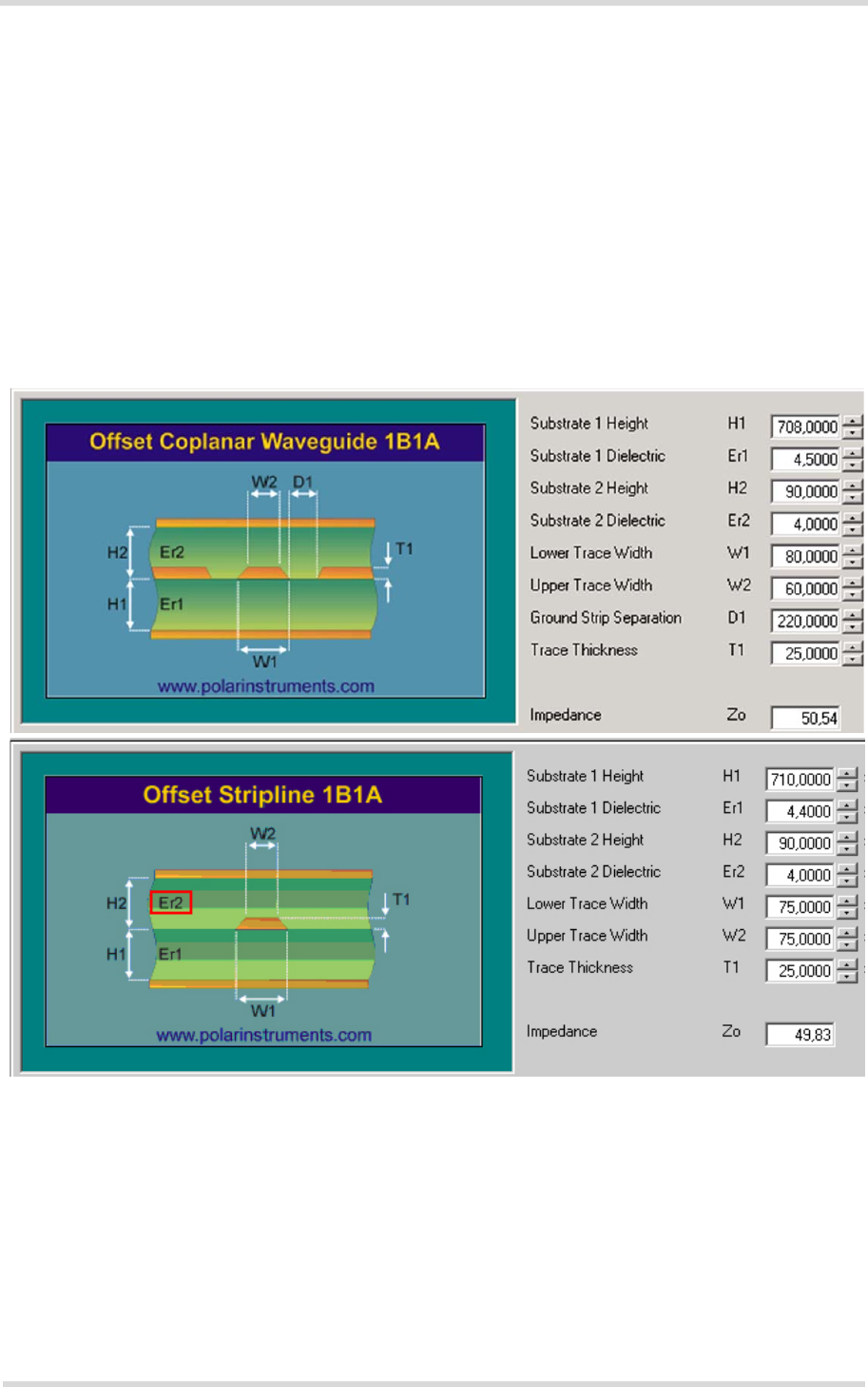
5.1.2.1 Line Arrangement Examples
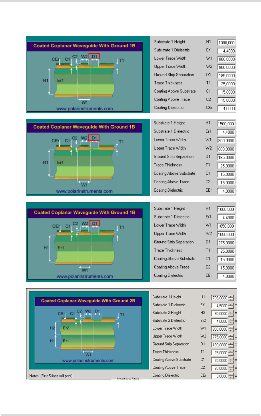
Several dedicated tools are available to calculate line arrangements for specific applications
and PCB materials - for example from http://www.polarinstruments.com/ (commercial software)
or from http://web.awrcorp.com/Usa/Products/Optional-Products/TX-Line/ (free software).
Embedded Stripline
This below figure shows line arrangement examples for embedded stripline.
Figure 7: Embedded Stripline line arrangement
Cinterion® ALS3-US R4 Hardware Interface Overview
5.1 GSM/UMTS/LTE Antenna Interface
34
ALS3-USR4_HIO_v03.915 2017-03-27
Confidential / Preliminary
Page 32 of 44
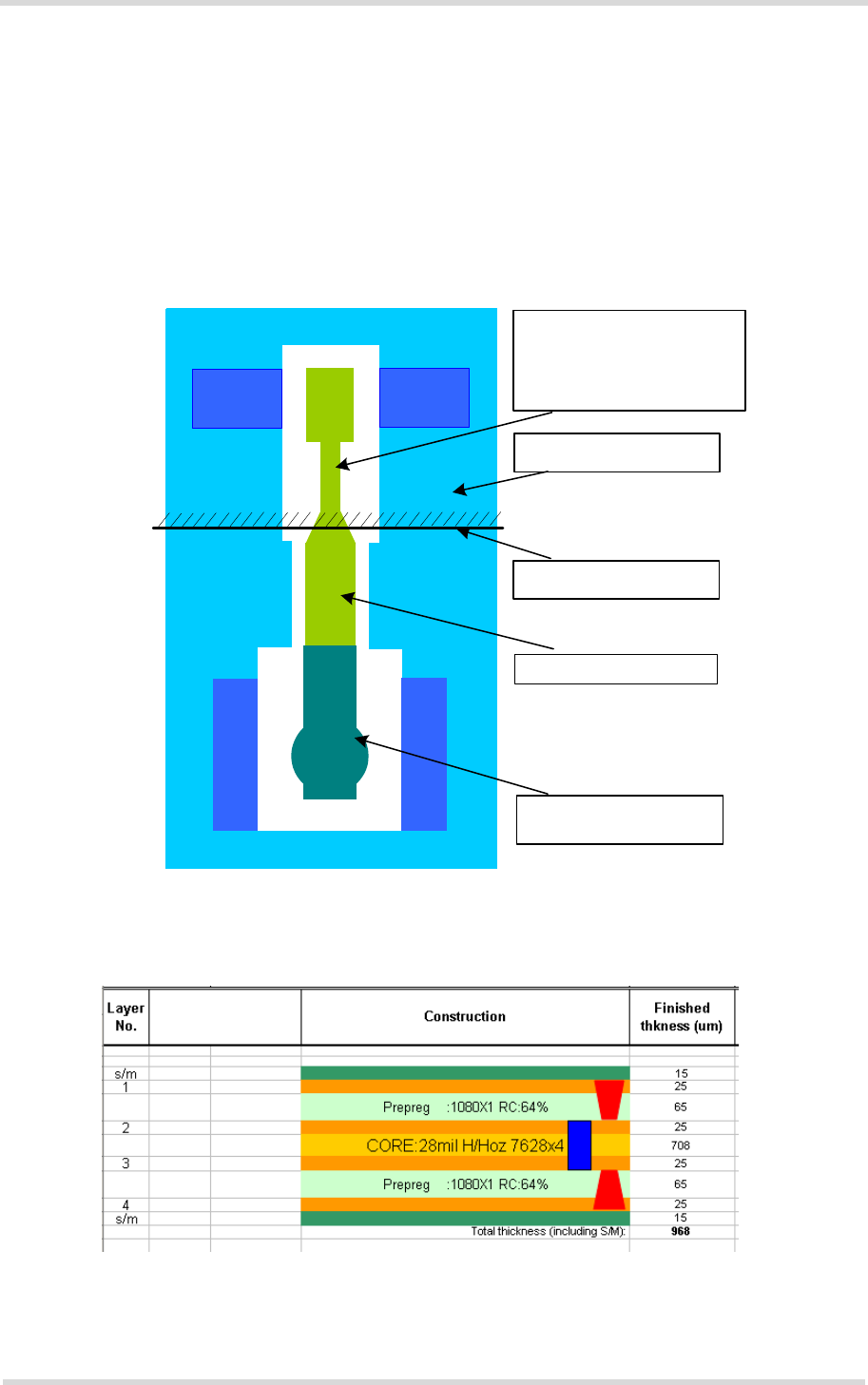
5.1.2.2 Routing Example
Interface to RF Connector
Figure 9 shows a sample connection of a module‘s antenna pad at the bottom layer of the mod-
ule PCB with an application PCB‘s coaxial antenna connector. Line impedance depends on line
width, but also on other PCB characteristics like dielectric, height and layer gap. The sample
stripline width of 0.33mm is recommended for an application with a PCB layer stack resembling
the one of the ALS3-US R4 evaluation board shown in Figure 10. For different layer stacks the
stripline width will have to be adapted accordingly.
Figure 9: Routing to application‘s RF connector
Figure 10: ALS3-US R4 evaluation board layer table
e.g.
ANT_
MAIN
G N D G N D
Edge of module PCB
Stripline (50 ohms) on top
layer of evaluation board from
antenna pad to module edge
Width = 0.33 mm
E.g., U.FL antenna
connector
50 ohms microstrip line
G N D G N D
Ground connection
Cinterion® ALS3-US R4 Hardware Interface Overview
5.2 GNSS Antenna Interface
34
ALS3-USR4_HIO_v03.915 2017-03-27
Confidential / Preliminary
Page 33 of 44
5.2 GNSS Antenna Interface
In addition to the RF antenna interface ALS3-US R4 also has a GNSS antenna interface. The
GNSS pad itself is the same as for the RF antenna interface (see Section 5.1.1).
It is possible to connect active or passive GNSS antennas. In either case they must have 50
impedance. The simultaneous operation of GSM/UMTS/LTE and GNSS is implemented.
ALS3-US R4 provides the supply voltage VGNSS for the GNSS active antenna (3.05V). It has
to be enabled by software when the GNSS receiver becomes active, otherwise VGNSS should
be off (power saving). VGNSS is not short circuit protected. This will have to be provided for by
an external application. The DC voltage should be fed back via ANT_GNSS_DC for coupling
into the GNSS antenna path. Figure 11 shows the flexibility in realizing the power supply for an
active GNSS antenna by giving two sample circuits realizing the supply voltage for an active
GNSS antenna - one with short circuit protection and one with an external LDO employed.
Figure 11: Supply voltage for active GNSS antenna
Short circuit
protection
(Imax=50mA)
VGNSS
ANT_GNSS
Active
GNSS
antenna
10nH
100nF
To GNSS
receiver
Module
SMT interface
ANT_GNSS_DC
typ 3.05V max. 50mA
Not short circuit protected!
1uF
(Optional)
ESD
protection
10k
Supply with short circuit protection
LDO
VGNSS
ANT_GNSS
Active
GNSS
antenna
10nH
100nF
To GNSS
receiver
Module
SMT interface
ANT_GNSS_DC
1uF
(Optional)
ESD
protection
10k
Enable
External
voltage
Supply with external LDO employed
Cinterion® ALS3-US R4 Hardware Interface Overview
5.2 GNSS Antenna Interface
34
ALS3-USR4_HIO_v03.915 2017-03-27
Confidential / Preliminary
Page 34 of 44
Figure 12 shows sample circuits realizing ESD protection for a passive GNSS antenna.
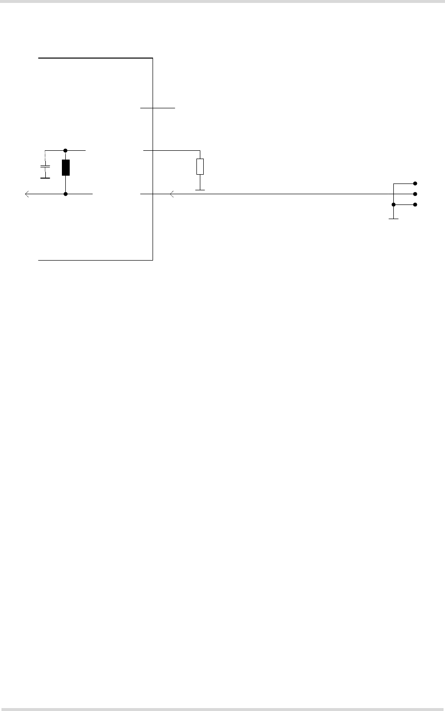
Figure 12: ESD protection for passive GNSS antenna
VGNSS
ANT_GNSS
Passive
GNSS
antenna
10nH
100nF
To GNSS
receiver
Module
SMT interface
ANT_GNSS_DC (Optional)
ESD
protection
0R
Not used
Cinterion® ALS3-US R4 Hardware Interface Overview
6 Mechanics
36
ALS3-USR4_HIO_v03.915 2017-03-27
Confidential / Preliminary
Page 35 of 44
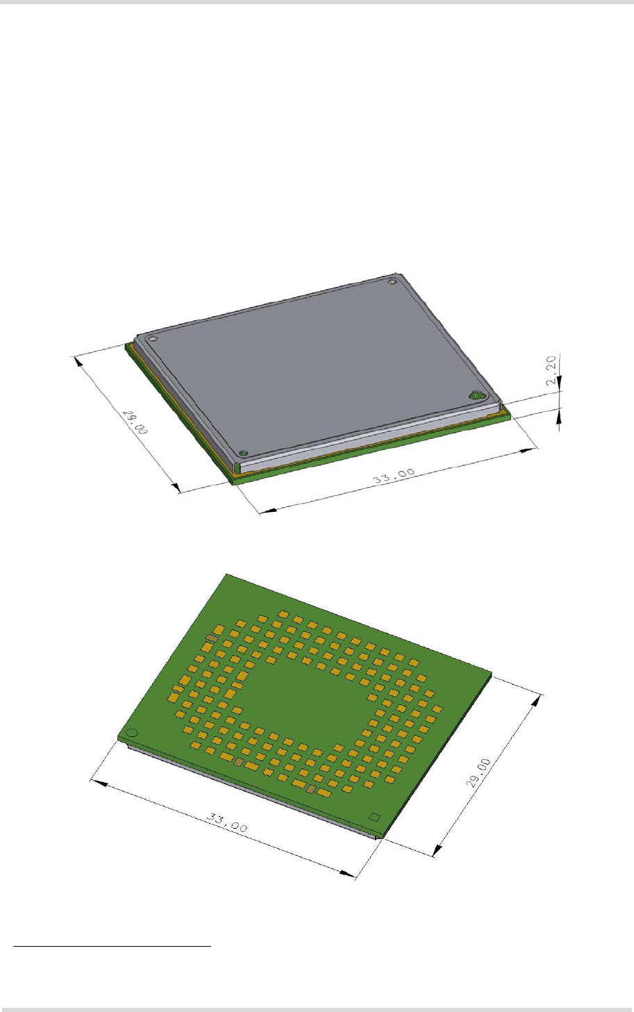
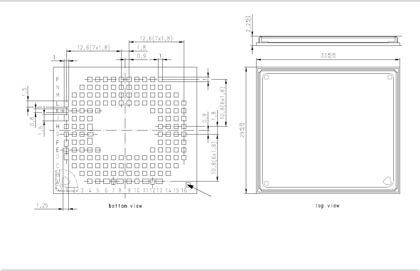
6 Mechanics
6.1 Mechanical Dimensions of ALS3-US R4
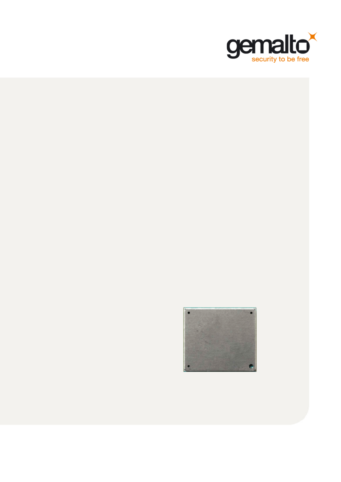
Figure 13 shows a 3D view1 of ALS3-US R4 and provides an overview of the board's mechan-
ical dimensions. For further details see Figure 14.
Length: 33mm
Width: 29mm
Height: 2.2mm
Figure 13: ALS3-US R4 – top and bottom view
1. The coloring of the 3D view does not reflect the module’s real color.
Top view
Bottom view

Cinterion® ALS3-US R4 Hardware Interface Overview
7 Sample Application
38
ALS3-USR4_HIO_v03.915 2017-03-27
Confidential / Preliminary
Page 37 of 44
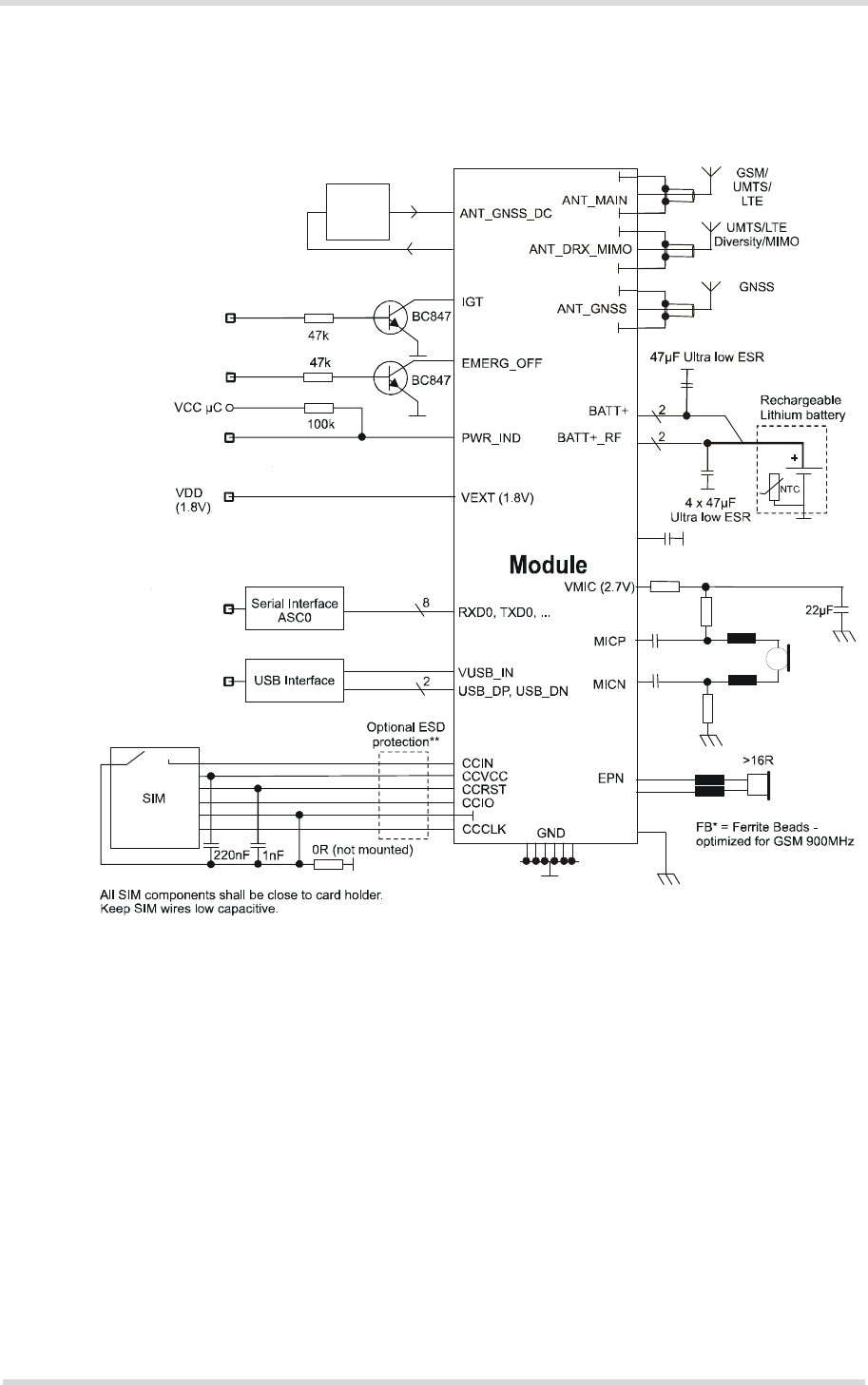
7 Sample Application
Figure 15 shows a typical example of how to integrate an ALS3-US R4 module with an appli-
cation.
The audio interface demonstrates the balanced connection of microphone and earpiece. This
solution is particularly well suited for internal transducers.
The PWR_IND line is an open collector that needs an external pull-up resistor which connects
to the voltage supply VCC µC of the microcontroller. Low state of the open collector pulls the
PWR_IND signal low and indicates that the ALS3-US R4 module is active, high level notifies
the Power Down mode.
If the module is in Power Down mode avoid current flowing from any other source into the mod-
ule circuit, for example reverse current from high state external control lines. Therefore, the
controlling application must be designed to prevent reverse flow.
While developing SMT applications it is strongly recommended to provide test points
for certain signals, i.e., lines to and from the module - for debug and/or test purposes.
The SMT application should allow for an easy access to these signals. For details on
how to implement test points see [3].
The EMC measures are best practice recommendations. In fact, an adequate EMC strategy for
an individual application is very much determined by the overall layout and, especially, the po-
sition of components.
Some LGA pads are connected to clocks or high speed data streams that might interfere with
the module’s antenna. The RF receiver would then be blocked at certain frequencies (self in-
terference). The external application’s PCB tracks connected to these pads should therefore
be well shielded or kept away from the antenna. This applies especially to the USB and UICC/
SIM interfaces.
Disclaimer:
No warranty, either stated or implied, is provided on the sample schematic diagram shown in
Figure 15 and the information detailed in this section. As functionality and compliance with na-
tional regulations depend to a great amount on the used electronic components and the indi-
vidual application layout manufacturers are required to ensure adequate design and operating
safeguards for their products using ALS3-US R4 modules.
Cinterion® ALS3-US R4 Hardware Interface Overview
8 Reference Approval
41
ALS3-USR4_HIO_v03.915 2017-03-27
Confidential / Preliminary
Page 39 of 44
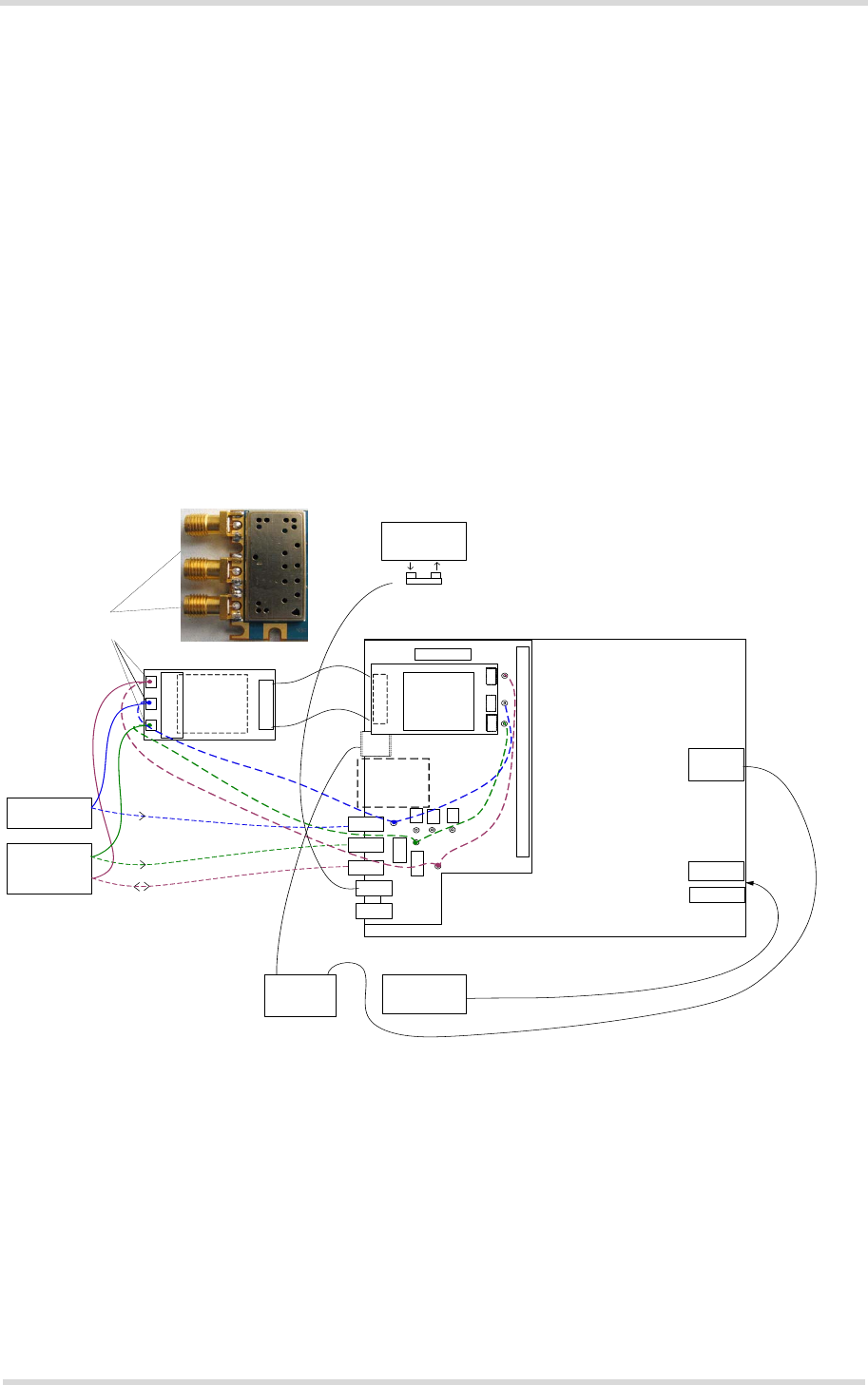
8 Reference Approval
8.1 Reference Equipment for Type Approval
The Gemalto M2M reference setup submitted to type approve ALS3-US R4 is shown in Figure
16. The module (i.e., the evaluation module) is connected to the DSB75 by means of a flex ca-
ble and a special DSB75 adapter. The GSM/UMTS/LTE test equipment is connected via edge
mount SMA connectors soldered to the module’s antenna pads.
For ESD tests and evaluation purposes, it is also possible connect the module to the GSM/
UMTS/LTE test equipment through an SMA-to-Hirose-U.FL antenna cable and the SMA anten-
na connectors of the DSB75 adapter.
A further option is to mount the evaluation module directly onto the DSB75 adapter’s 80-pin
board-to-board connector and to connect the test equipment as shown below.
Figure 16: Reference equipment for type approval
DSB75
Standard
80 polig Flex
PC
GSM/UMTS/LTE
test equipment
GSM/UMTS/LTE
USB
cable
Power
supply
Power
GND
USB
ANT3
ANT2
ANT1
Audio
Uranus
Audio
DSB75 adapter
SIM card
holder
Evaluation
module
Edge mount SMA connectors
manually soldered to antenna pads
Detail:
SMA to Hirose U.FL cable
UMTS/LTE Rx Diversity/
MIMO
Evaluation
module
GNSS
test equipment
COM1
(ASC0)
Audio
test equipment
Votronic
handset
If using analog audio
Cinterion® ALS3-US R4 Hardware Interface Overview
8.2 Compliance with FCC and IC Rules and Regulations
41
ALS3-USR4_HIO_v03.915 2017-03-27
Confidential / Preliminary
Page 40 of 44
8.2 Compliance with FCC and IC Rules and Regulations
The Equipment Authorization Certification for the Gemalto M2M modules reference application
described in Section 8.1 will be registered under the following identifiers:
•ALS3-US R4:
FCC Identifier QIPALS3-USR4
Industry Canada Certification Number: 7830A-ALS3USR4
Granted to Gemalto M2M GmbH
Manufacturers of mobile or fixed devices incorporating ALS3-US R4 modules are authorized
to use the FCC Grants and Industry Canada Certificates of the ALS3-US R4 modules for their
own final products according to the conditions referenced in these documents. In this case, the
FCC label of the module shall be visible from the outside, or the host device shall bear a second
label stating "Contains FCC ID: QIPALS3-USR4" and accordingly “Contains IC: 7830A-
ALS3USR4“. The integration is limited to fixed or mobile categorized host devices, where a
separation distance between the antenna and any person of min. 20cm can be assured during
normal operating conditions.
For mobile and fixed operation configurations the antenna gain, including cable loss, must not
exceed the limits listed in the following Table 10 for FCC and IC.
IMPORTANT:
Manufacturers of portable applications incorporating ALS3-US R4 modules are required to
have their final product certified and apply for their own FCC Grant and Industry Canada Cer-
tificate related to the specific portable mobile. This is mandatory to meet the SAR requirements
for portable mobiles (see Section 1.4 for detail).
Changes or modifications not expressly approved by the party responsible for compliance
could void the user's authority to operate the equipment.
Table 10: Antenna gain limits for FCC and IC
Operating band FCC limit IC limit Unit
Maximum gain in lower operating bands with f< 1GHz
(GSM850, WCDMA BdV, LTE Bd5 / Bd17 3.25 0.18 dBi
Maximum gain in higher operating bands with f=1700MHz
(WCDMA BdIV, LTE Bd4) 5.5 5.5 dBi
Maximum gain in higher operating bands with f=1900MHz
(GSM1900, WCDMA BdII, LTE Band 2) 2.51 2.51 dBi

Cinterion® ALS3-US R4 Hardware Interface Overview
8.2 Compliance with FCC and IC Rules and Regulations
41
ALS3-USR4_HIO_v03.915 2017-03-27
Confidential / Preliminary
Page 41 of 44
Note: This equipment has been tested and found to comply with the limits for a Class B digital
device, pursuant to part 15 of the FCC Rules and with Industry Canada license-exempt RSS
standard(s). These limits are designed to provide reasonable protection against harmful inter-
ference in a residential installation. This equipment generates, uses and can radiate radio fre-
quency energy and, if not installed and used in accordance with the instructions, may cause
harmful interference to radio communications. However, there is no guarantee that interference
will not occur in a particular installation. If this equipment does cause harmful interference to
radio or television reception, which can be determined by turning the equipment off and on, the
user is encouraged to try to correct the interference by one or more of the following measures:
• Reorient or relocate the receiving antenna.
• Increase the separation between the equipment and receiver.
• Connect the equipment into an outlet on a circuit different from that to which the receiver
is connected.
• Consult the dealer or an experienced radio/TV technician for help.
This Class B digital apparatus complies with Canadian ICES-003.
If Canadian approval is requested for devices incorporating ALS3-US R4 modules the above
note will have to be provided in the English and French language in the final user documenta-
tion. Manufacturers/OEM Integrators must ensure that the final user documentation does not
contain any information on how to install or remove the module from the final product.
Cinterion® ALS3-US R4 Hardware Interface Overview
9 Appendix
43
ALS3-USR4_HIO_v03.915 2017-03-27
Confidential / Preliminary
Page 42 of 44
9 Appendix
9.1 List of Parts and Accessories
Table 11: List of parts and accessories
Description Supplier Ordering information
ALS3-US R4 Gemalto M2M Standard module
Gemalto M2M IMEI:
Packaging unit (ordering) number: L30960-N3480-A400
Module label number: S30960-S3480-A400-11
1. Note: At the discretion of Gemalto M2M, module label information can either be laser engraved on the
module’s shielding or be printed on a label adhered to the module’s shielding.
ALS3-US R4
Evaluation module Gemalto M2M Ordering number: L30960-N3481-A400
DSB75 Support Box Gemalto M2M Ordering number: L36880-N8811-A100
DSB75 adapter for mount-
ing the evaluation module Gemalto M2M Ordering number: L30960-N2301-A100
Votronic handset for
approval purposes Votronic /
Gemalto M2M Gemalto M2M ordering number: L36880-N8301-A107
Votronic ordering number: HH-SI-30.3/V1.1/0
Votronic
Entwicklungs- und Produktionsgesellschaft für elek-
tronische Geräte mbH
Saarbrücker Str. 8
66386 St. Ingbert
Germany
Phone: +49-(0)6 89 4 / 92 55-0
Fax: +49-(0)6 89 4 / 92 55-88
Email: contact@votronic.com
SIM card holder incl. push
button ejector and slide-in
tray
Molex Ordering numbers: 91228
91236
Sales contacts are listed in Table 12.
U.FL antenna connector Hirose or
Molex Sales contacts are listed in Table 12 and Table 13.

Cinterion® ALS3-US R4 Hardware Interface Overview
9.1 List of Parts and Accessories
43
ALS3-USR4_HIO_v03.915 2017-03-27
Confidential / Preliminary
Page 43 of 44
Table 12: Molex sales contacts (subject to change)
Molex
For further information please click:
http://www.molex.com
Molex Deutschland GmbH
Otto-Hahn-Str. 1b
69190 Walldorf
Germany
Phone: +49-6227-3091-0
Fax: +49-6227-3091-8100
Email: mxgermany@molex.com
American Headquarters
Lisle, Illinois 60532
U.S.A.
Phone: +1-800-78MOLEX
Fax: +1-630-969-1352
Molex China Distributors
Beijing,
Room 1311, Tower B, COFCO Plaza
No. 8, Jian Guo Men Nei Street, 100005
Beijing
P.R. China
Phone: +86-10-6526-9628
Fax: +86-10-6526-9730
Molex Singapore Pte. Ltd.
110, International Road
Jurong Town,
Singapore 629174
Phone: +65-6-268-6868
Fax: +65-6-265-6044
Molex Japan Co. Ltd.
1-5-4 Fukami-Higashi,
Yamato-City,
Kanagawa, 242-8585
Japan
Phone: +81-46-265-2325
Fax: +81-46-265-2365
Table 13: Hirose sales contacts (subject to change)
Hirose Ltd.
For further information please click:
http://www.hirose.com
Hirose Electric (U.S.A.) Inc
2688 Westhills Court
Simi Valley, CA 93065
U.S.A.
Phone: +1-805-522-7958
Fax: +1-805-522-3217
Hirose Electric Europe B.V.
German Branch:
Herzog-Carl-Strasse 4
73760 Ostfildern
Germany
Phone: +49-711-456002-1
Fax: +49-711-456002-299
Email: info@hirose.de
Hirose Electric Europe B.V.
UK Branch:
First Floor, St. Andrews House,
Caldecotte Lake Business Park,
Milton Keynes MK7 8LE
Great Britain
Phone: +44-1908-369060
Fax: +44-1908-369078
Hirose Electric Co., Ltd.
5-23, Osaki 5 Chome,
Shinagawa-Ku
Tokyo 141
Japan
Phone: +81-03-3491-9741
Fax: +81-03-3493-2933
Hirose Electric Europe B.V.
Hogehillweg 8
1101 CC Amsterdam Z-O
Netherlands
Phone: +31-20-6557-460
Fax: +31-20-6557-469

44
M2M.GEMALTO.COM
About Gemalto
Gemalto (Euronext NL0000400653 GTO) is the world leader in digital security with 2015 annual
revenues of €3.1 billion and blue-chip customers in over 180 countries. Our 14,000+ employees
operate out of 118 offices, 45 personalization and data centers, and 27 research and software
development centers located in 49 countries.
We are at the heart of the rapidly evolving digital society. Billions of people worldwide increasingly
want the freedom to communicate, travel, shop, bank, entertain and work - anytime, everywhere
- in ways that are enjoyable and safe. Gemalto delivers on their expanding needs for personal
mobile services, payment security, authenticated cloud access, identity and privacy protection,
eHealthcare and eGovernment efficiency, convenient ticketing and dependable machine-to-
machine (M2M) applications.
Gemalto develops secure embedded software and secure products which we design and
personalize. Our platforms and services manage these secure products, the confidential data they
contain and the trusted end-user services they enable. Our innovations enable our clients to offer
trusted and convenient digital services to billions of individuals.
Gemalto thrives with the growing number of people using its solutions to interact with the digital
and wireless world.
For more information please visit
m2m.gemalto.com, www.facebook.com/gemalto, or Follow@gemaltom2m on twitter.
Gemalto M2M GmbH
Werinherstrasse 81
81541 Munich
Germany
© Gemalto 2017. All rights reserved. Gemalto, the Gemalto logo, are trademarks and service marks of Gemalto and are registered in certain countries. April 2013