Genex Telecom SD5200 RF Data Radio Transceiver User Manual SD 5200 service manual
Genex Telecom Co., Ltd. RF Data Radio Transceiver SD 5200 service manual
revised users manual
TEKK INC.
SD-5200 MANUAL
5/2 WATT RF DATA RADIO

IMPORTANT NOTICE!
FCC RF Exposure Compliance requirements for Occupational Use:
• This device must be restricted to work related operations in an occupational / controlled RF exposure
environment.
• Transmitting duty factor may not exceed 50%.
• All qualified users must have the knowledge to control their own, passengers and bystanders ’RF
exposure to comply with the General Population / Controlled MPE limit and requirements.
• The antenna used for this transmitter must be installed to provide a separation distance of at least 32cm
from all persons and must not exceed an antenna gain of 0 dDd.
IMPORTANT NOTICE!
This radio can only be programmed to frequency by qualified, approved technicians using a separate PC
software and cable package. Only authorized technicians can contact Tekk to purchase this programming
software product.
CH.1 PRODUCT INTRODUCTION
SD-5200, This RF Data Radio is designed to operate in the frequency range is 450MHz~ 470MHz. Inside of SD-5200 is
installed microprocessor and SD-5200 is operated by PLL type. RF power is 2watt and 5watt. Bandwidth is 12.5khz or
25khz
SD-5200 features
-. PLL SYNTHESIZER type
-. set parameter with PC program
-. RF power : 2 Watt, 5Watt
-. band width : 12.5/25kHz
-. light weight
-. PC downloading
-. Power : DC 10V
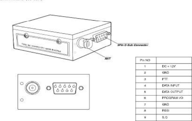
2. SD-5200 outward view
Data Radio (SD-5200)
3. D-SUB Connector PIN Specification
PIN NO PIN Specification Remark
1 DC+12V 9V~15V
2 GND
3 PTT “Low" Active
4 DATA INPUT
5 DATA OUTPUT
6 S_I/O( PC Program) Programming
7 GND
8 RSSI Receive Signal Strength Indicator
9 S.Q(CD) Carrier Detect
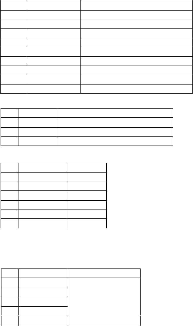
4. CON2 PIN Specification (PCB Connector)
PIN NO
PIN Specification
Remark
1 RSSI Receive Signal Strength Indicator
2 GND
3 S_I/O PC Program PIN
5. CON3 PIN Specification (PCB Connector)
6. CON4 PIN Specification (PCB Connector)
CH2. SPECIFICATIONS
PIN NO
PIN Specification Remark
1 S.Q (C.D)
2 DATA INPUT
3 DATA OUTPUT
4 PTT
5 DC+12V
6 GND
PIN NO
PIN Specification Remark
1 RESET
2 DC+5V
3 S_CLOCK
4 S_DATA
5 GND
used
for modifying
MPU Program
1. Specification
GENERAL
Operating Mode
Frequency Range
Frequency Stability
Programmable Channels
Channel Spacing
Dimensions
Weight
Power Source
Current Drain(maximum)
Conventional (nontrunked) only
450~470MHz
±2.5PPM(-30 to +60?)
1 Channel
Dual Channel Spacing 12.5/25kHz
30mm(H)×60mm(W)×95mm(L)
360g
DC 9~15V
Transmit mode - 1.8A
RECEIVER
Sensitivity
Squelch Sensitiviy
Selectivity
Spurious and Harmonic
Rejection
Intermodulation
FM Hum and Noise
Maximum Frequency Spread
Audi o Output Power
Audio Distortion
Audio Response
IF Frequencies
Input Impedance
.35uV 12 dB SINAD
.25uV 10dB SINAD
-60dB (12.5KHz)
-60dB (25KHz)
-60dB
-60dB
-34dB(12.5KHz), -40dB(25KHz)
UHF = 20MHz
460mW across an 8-ohm load
Less than 5% at rated output
±2dB from characteristic from 20~3000Hz
21.4MHz and 455kHz
50 ohms
TRANSMITTER
RF Power Output
Spurious and Harmonic
FM Hum and Noise
Audio Distortion
Audio Frequency Response
Maximum Channel Spread
Output Impedance
2 Watt or 5 Watt
-60
-34dB(12.5KHz), -40dB(25KHz)
5% maximum with 1kHz modulation
±2dB from characteristic from 20~3000Hz
UHF = 20MHz
50 ohms
CH. 3 SD-5200 circuit
1. SD-5200 circuit
SD-5200 circuit is composed of RF and MPU. (RF determines communication quality and performance. MPU controls
terminal performance.) RF is composed of TX and RX. TX is composed of synthesizer (Synthesizer generates TX
frequency.), VCO, Data ALC (Automatic Level Control), Power Drive, final amplification and antenna switch.
RX is composed of front-end, mixer, local drive, and crystal filter. IF amplifier, IF IC and Data conduct.
MPU is composed of EEPROM storing parameter of controls in the SD-5200.
2. Transmit
2.1 SYNTHESIZER
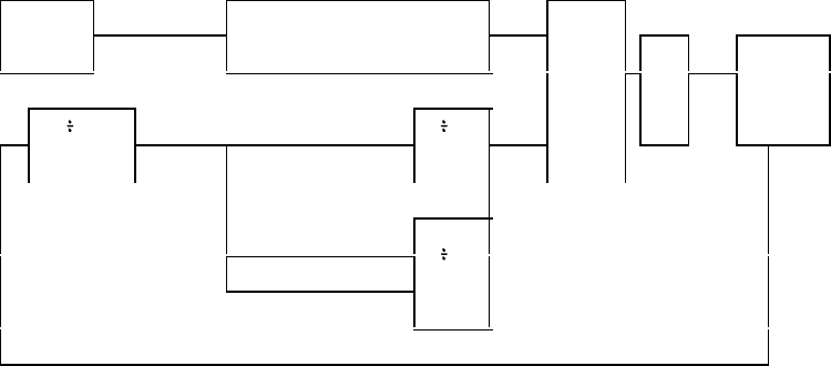
Synthesizer is consisting of TCXO, PLL IC, Charge Pump, LPF and VCO. See illustration 2-1.
TCXO (U17) plays a key role to make usable frequency for terminal and uses a 14.4MHz(-30?C~+60?C, 2.5ppm) of
VX-23VA in JVC co. It uses resistance R65, R66 and VR13 externally for accuracy of frequency and modulation of low
frequency data signal. When VR13 is turned to '+', voltage increases and frequency lowers. When VR13 is turned to '-',
frequency rises.
If TX or RX frequency deviation occurs, you can control with VR13.
Inside of PLL IC, there are 4 Divider Registers (CH1, CH2 Programmable Divider, Reference Divider and Option Control).
Now, SD-2000N/5200 use only CH1 Programmable Divider
2.1.1 Composition of Divider Register
Inside of PLL IC consistsof 4 Registers and is set with code.
14.4MHz fR
TCXO
U104
Reference
Counter
fV
Loop
Filter
VCO
64
Prescaler
N
Counter
Phase
Detector
A
Counter
Illustration 2-1 Composition of Synthesizer
COD
E ITEM
1 0 Number of dividers by CH1 Programmable divider(Fin1)
0 1 Number of dividers by CH2 Programmable divider(Fin2)
1 1 Number of dividers by reference divider(Xin)
0 0 Option control
1) Programmable divider
LSB MSB
A0
A1
A2
A3
A4
D0
D1 D2
D3
D4 D5
D6
D7
D8
D9
D10
D11
1 0
Calculation for generating 450.0125 MHz frequency, as below.
Set basic channel as 6.25 KHz.
450.0125 MHz ÷ 6.25 KHz = 72002
N and A Counter values are 72002 ÷ 64 = 1125. 03125
N value = 1125 ? 465 hex
A value = 0.3125 ? 0.3125 x 64 = 20 ? 14 hex
LSB 4 1 5 6 4 MSB
2) Reference Divider
LSB MSB
Calculation for basic frequency of 6.25 KHz with TCXO frequency
14.4 MHz ÷ 6.25 KHz = 2304 ? 900 hex
0
0
1
0
1
1
0
1
0
0
1
1
0
0
0
1
0
1
0
D0
D1
D2
D3
D4
D5
D6
D7
D8
D9
D10
D11
1
1
LSB 0 0 9 MSB
3) Option Control
T CP CP1
CP2
SB1
CP1
CP2
SB2
SBR
LD1
LD2
SW 0 0
T : Test Mode (always "0")
CP : Charge pump output polarity
CP Output Polarity
0 Normal
1 Reverse
Charge Pump Output Current
Lock detector output
Control bit
SB1 SB2
LD1 LD2
Lock detector output state
0 0 L
0 1 CH2 only detector
1 0 CH1 only detector
0 0
1 1 CH1, CH2
0 0 L
0 1 H
0
0
0
0
0
0
0
0
1
0
0
1
1
1
Control bit
CP1
CP2
Charge pump
output current
0 0 100 µA
0 1 200 µA
1 0 400 µA
0 0 800 µA
1 0 CH2 only detector
1 1 CH1 only detector
0 0 L
0 1 CH2 only detector
1 0 H
1 0
1 1 CH1 only detector
0 0 L
0 1 H
1 0 H
1 1
1 1 H
Filter Switch Control
On CH1, data for checking PLL Lock, as below.
0 0 1 1 0 0 0 1 0 1 0 0 0 0
2.2 VCO
VCO is circuit with Colpitts Oscillator, oscillates with control voltage by synthesizer and consist of TX and RX.
RX VCO is operating when RX VCO power Switch, TR(Q28) turns on. TX VCO is operating when TX VCO power Switch,
TR Q27) turns on. Control voltage of VCO change pulse voltage generated in Charge Pump of PLL IC to DC voltage as
passing Low Pass Filter (C70, C71, C72, R69, R70).
Frequency range by control power, as table 3.1.
SW
Output
0 OFF
1 ON
MODEL
PLL Control Power Range
frequency range remark
TX 1.3 ~ 4.5 V 450 ~ 470 MHz
SD-5200
RX 1.3 ~ 4.5 V 428.6 ~448.6MHz
Table 3.1: Control power and frequency
Operation for transmit Mode is oscillated by Q21, C84, C85, C86, C87, C88, C89, C90, C91, VC12, D15, D16 and L26
They are consist of Colpitts Oscillator.).
R7 and C86 are circuit to remain 450 ~ 470 MHz frequency stable.
Varicap Diode determines frequency range for D15. D16 alters Data.
Operation for Receive Mode is oscillated by Q20, C73, C74, C75, C76, C77, C78, C79, D14 and L21.
Q22 and extra parts are buffers to amplify RF carrier which is oscillated by TX VCO and RX VCO, remain final output
0dBm±2dB and prevent amplified reverse power from output part.
2.3 Input Data ALC (Automatic Level Control)
User can use different input signal level.
Input Data ALC (Automatic Level Control) is designed to use every digital signal whose input signal range is 05V~0.6V.
Input signal data provided by D-sub Connector No. 4 pin amplify 47times as U16A and is provided to U16B Limiting
circuit. Output of U16B restricts every signal as 1.4V and provides to VCO and TCXO. TCXO (U17) alters data signal
(0~350Hz) with R63 and C64 and does not alter more than 350Hz with VCO. R60 is used as bypass, not using input
Data ALC(Automatic Level Control)circuit.
2.4 POWER DRIVE
TX Drive (Q24, Q25) amplify RF power occurring VCO to meet final AMP input and restrict influence of reverse power.
First amp (Q24) operate as A level and amplify VCO output about 15dB. Second amp(Q25) amplify about 10dB to
amplify final AMP(Q26) about 5W and to remain final output of C107 24~25dB. When P2.6 Port of MPU (U13) is high,
Q24 and Q25 turn Q31 on and TR(Q30) provide power to TX drive.
This power provides power to ANT S/W and turn on D10 and D11 to emit TX carrier through antenna.
2.5 Final AMP and APC
Final TR (Q26) amplify RF Carrier as much as around 15dBm in the finial part of amplification. R96, VR14 and Q33
decide TX Power. Q33 and VR alter SD-5200 from 5W to 2W. When MPU (U13) becomes high, Q33 will be "ON" by
dropping the gate pow er of TR (Q26).
When MPU (U13) P1.0 Port becomes High, Q33 will be ON, and alter power form 5W to 2W by dropping gate power of
final TR(Q26) VR14 will control 2W RF power.
APC is designed to be operated when power is 2W
APC senses RF carrier from Final AMP and low supply power when RF Power is higher more than 2W. When RF Power
is less than 2W, APC increase supply power of power Drive in order to make RF Power maintain 2W.
APC (Automatic Power Control) consist of RF Carrier sensor, amplification part that compare with standard voltage and
schematic that switch the checked voltage.
RF Carrier sensor will be changed to DC voltage by using C116, D20, C134 in order to supply base voltage of Q36 in the
amplification part.
The voltage which is supplied to Q36 is arrange low power(2W) with VR14, High Power(5W) control Q33 (when Base is
high).
Q36 in the amplification compare base voltage of Q36 which come from sensor part with base standard voltage which is
supplied to Q36 and control Q35 which control RF pow er to be 2W by controlling base voltage of Q30.
2.6 Antenna Switch
Antenna switch is consist of TX carrier, switching part and low pass filter. Switching part choose RF RX signal and low
pass filter eliminate spurious at TX.
TX and RX switching part is operated by Pin Diode D10, D11.
At TX, when TX+8V provide power to L36, R98 and C113, D10 and D11 turn on, RF carrier flowing receiving direction is
isolated and emit to antenna. At RX, when power providing to Pin diode of TX+8V turn off, D10 and D11 turn off and RF
carrier is provided to receiving direction.

Low Pass Filter eliminate needless spurious and is consist of 2 steps.
3. Receive
3.1 FRONT-END
Front-end choose and amplify bandwidth of RF signal. Front end is consist of filter and LNA (Low Noise Amp). LNA is
consist of two Transistors (Q10, Q11) and amplify about 20dB. Filter use two SAW Filter (F9. F10) to remain bandwidth
of 450~470MHz. When P0.1 is high, TR Q4 turn on, Band Switching Diode (D18, D19) turn off, F9 turn off and F10 turn
on. Band Width of SAW Filter, as below.
3.2 Mixer
Mixer (Q12) mix received RF signal and local
signal from synthesizer and then generate
21.4MHz, IF frequency. Volume of local signal
is -4dBm at maximum and Conversion Gain about 2dBm.
Medium frequency is determined, as below.
FIF = FRF ± FLOCAL
For preventing spurious. n-Channel Dual Gate MOS-FET, BF998 is used and spurious level of Local and RX RF is less
than -70dB
m.
3.3 Crystal filter and IF AMP
Pass Band Width of 21.4MHz X-TAL filter(F11) is ±6KHz and can use 12.5KHz and 25KHz Spec of MCF : Ripple -
1dB, Insertion Loss - 3dB, MCF reduce about -35dB far from ±20KHz.
IF AMP(Q13) amplify X-TAL filter in 21.4MHz as 25dB. Consumption of voltage is less than 5mA.
3.4 IF IC
IF IC (U11) is consist of second Mixer, Ceramic Filter, 455KHz Resonator, Noise Squelch and SRRI.
Second Mixer generate 455KHz, mixing IF 21.4MHz and 2nd Local 20.945MHz(X10). This signal catches the Ceramic
Filter (F13, F14) with 12.5/25KHz switch (D12, D13) and determines adjacent channel fitting with 12.5/25KHz.
Channel selection in 12.5/25KHz is operated by MPU (U13) P0.4.
SAW Filter P0.1 frequency range
F9 Low 460~470 MHz
F10 High 450~460 MHz

When P0.4 is high, 25KHz(F13) is selected. When P0.4 is low, 12.5KHz(F14) sis selected.
455KHz Resonat or eliminate Carrier between received second IF Carrie and data signal and detect signal. In 25KHz,
Q14 turn on and reduce 455KHz Resonator to remain data signal stable volume of 12.5/25KHz.
Noise Squelch signal identically detect noise squelch signal in 12.5/25KHz. RSSI signal alters to voltage according to
signal strength inside of IF IC and provide D-SUB connector No. 8 pin.
3.5 Data Handling
Data handling part reverse or de-reverse signal at 2V with OP AMP (U12).
If users use TX data at 1/2 VCC voltage, user can use U12A No.1 pin (Invert Signal) or U12B No.7pin (Normal Signal).
After eliminating DC part, user can use as C48.
3.6 MPU (U13)
MPU operates after down loading RF status with D-SUB Connector No. 6 pin (S_I/O).
EEPROM (U14) stores Paramet er of every kind and provide information.
Each port for MPU as following table
Port 0 Port 0
P0.0 S_CLOCK P2.0 H/L_POW
P0.1 S-DATA/H/L_BAND P2.1 PLL_LOCK
P0.2 S_I/O P2.2 EEPORM DATA
P0.3 PTT P2.3 PLL_CLOCK/
EEPROM CLOCK
P0.4 12.5/25KHz P2.4 PLL_DATA
P0.5 RX_CON P2.5 PLL_ENABLE
P0.6 TX_VCO P2.6 TX_POW
P0.7 RX_VCO