Geniatech 17D11C6 Developer Board User Manual Hardware Manual
Shenzhen Geniatech INC.,LTD. Developer Board Hardware Manual
User Manual

Developer Board 4 Hub
UserGuide
Powered
by:

2
Contents
1
Introduction
.................................................................................................................................................................... 4
2
What’s
in
the
Box
............................................................................................................................................................. 7
3
Getting
started
................................................................................................................................................................. 8
3.1
Prerequisites
.......................................................................................................................................................... 8
3.2
Starting
the
board
for
the
first
time
......................................................................................................................... 8
4
DB4
Overview
.................................................................................................................................................................. 9
4.1
System
Block
diagram
............................................................................................................................................. 9
4.2
Processor
.............................................................................................................................................................. 9
4.3
Memory
................................................................................................................................................................ 9
4.4
MicroSDHC
............................................................................................................................................................ 9
4.5
Ethernet
.............................................................................................................................................................. 10
4.6
WiFi/BT/RF
.......................................................................................................................................................... 10
4.7
Display
Interface
.................................................................................................................................................. 10
4.7.1
HDMI
......................................................................................................................................................... 10
4.7.2
MIPI-DSI
..................................................................................................................................................... 11
4.8
Camera
Interfaces
................................................................................................................................................ 11
4.9
USB
Ports
.............................................................................................................................................................. 11
4.9.1
USB-Host
ports
........................................................................................................................................... 11
4.9.2
USB-Device
port
.......................................................................................................................................... 12
4.10
Audio
................................................................................................................................................................ 12
4.10.1
BT
Audio
................................................................................................................................................... 12
4.10.2
HDMI
Audio
.............................................................................................................................................. 12
4.11
DC-power
and
Battery
Power
................................................................................................................................ 12
4.12
Measurements
.................................................................................................................................................... 13
4.13
Buttons
.............................................................................................................................................................. 13
4.14
External
Fan
connection
....................................................................................................................................... 13
4.15
UART
................................................................................................................................................................... 13
4.16
JTAG
.................................................................................................................................................................... 13
4.17
System
and
user
LEDs
........................................................................................................................................... 13
4.18
Expansion
Connector
........................................................................................................................................... 13
4.19
Additional
Functionality
....................................................................................................................................... 14
4.19.1
On
Board
Analog
Microphone
................................................................................................................... 14
4.19.2
Analog
Connector
..................................................................................................................................... 14
5
Low
speed
Expansion
connector
..................................................................................................................................... 15
5.1
UART
{0/1}
........................................................................................................................................................... 17
5.2
I2C
{0/1}
.............................................................................................................................................................. 17
5.3
GPIO
{A-L}
........................................................................................................................................................... 17

3
5.4
SPI
0
................................................................................................................................................................... 17
5.5
PCM/I2S
.............................................................................................................................................................. 17
5.6
Power
and
Reset
.................................................................................................................................................. 18
5.7
Power
Supplies
.................................................................................................................................................... 18
6
High
speed
expansion
connector
..................................................................................................................................... 19
6.1
MIPI
DSI
0
........................................................................................................................................................... 21
6.2
MIPI
CSI
{0/1}
...................................................................................................................................................... 21
6.3
I2C
{2/3}
............................................................................................................................................................... 21
6.4
HSIC
.................................................................................................................................................................... 22
6.5
Reserved
............................................................................................................................................................. 22
6.6
SD/SPI
................................................................................................................................................................. 22
6.7
Clocks
................................................................................................................................................................. 22
6.8
USB
.................................................................................................................................................................... 22
7
Analog
Expansion
Connector
............................................................................................................................................ 23
7.1
Speaker
............................................................................................................................................................... 23
7.2
Mic
..................................................................................................................................................................... 23
7.3
Headset
.............................................................................................................................................................. 23
7.4
FM
Antenna
........................................................................................................................................................ 23
8
Power
management
....................................................................................................................................................... 25
8.1
DC
Power
Input
................................................................................................................................................... 25
8.2
Power
Source
Selection
........................................................................................................................................ 25
8.3
Power
Consumption
............................................................................................................................................. 26
8.4 Power Sequencing
............................................................................................................................................... 26
8.5
Voltage
Rails
........................................................................................................................................................ 26
8.6
Power
Measurements
.......................................................................................................................................... 26
8.6.1
Power-In
measurement
............................................................................................................................... 26
8.6.2
PMIC
Power-In
measurement
...................................................................................................................... 26
9
Buttons
and
status
LED’s
................................................................................................................................................. 27
9.1
Buttons
............................................................................................................................................................... 27
9.1.1
Volume
up
.................................................................................................................................................. 27
9.1.2
Volume
down
............................................................................................................................................. 27
9.1.3
Power
Button
.............................................................................................................................................. 27
9.1.4
Reset
Button
............................................................................................................................................... 27
9.2
LED’s
................................................................................................................................................................... 27
9.2.1
User
LED
1-4
............................................................................................................................................... 27
9.2.2
Bluetooth
status
.......................................................................................................................................... 27
9.2.3
WiFi
status
................................................................................................................................................. 27
9.2.4 Ethernet status
........................................................................................................................................... 27
10
Boot
configuration
......................................................................................................................................................... 28
4
1
Introduction
The Developer Board 4 Hub(hereinafter referred to as DB4) is a 96Boards compliant community board based on Qualcomm®
Snapdragon 400 series of SoC’s.
The following table lists its key features:
Processor
Qualcomm Snapdragon 410
Quad-core ARM® Cortex® A53 at up to 1.2 GHz per core
64-Bit capable
Qualcomm Adreno 306 400MHz GPU for PC-class graphics with support for
advanced APIs, including OpenGL ES 3.0, OpenCL, DirectX, and content security
Memory/
Storage
1GB or 2GB LPDDR3 533MHz
8GB or 16GB eMMC 4.51
SD 3.0 (UHS-I)
Video 1080p@30fps HD video playback and capture with H.264 (AVC), and 720p playback
with H.265 (HEVC)
Camera Support Integrated ISP with support for image sensors up to 13MP
Audio PCM/AAC+/MP3/WMA, ECNS, Audio+ post-processing (optional)
Connectivity WLAN 802.11 b/g/n 2.4GHz
10/100M Ethernet
Bluetooth 4.1
One USB 2.0 micro B (device mode only)
Two USB 2.0 (host mode only)
On-board BT and WLAN antenna
I/O Interfaces One 40-pin Low Speed (LS) expansion connector
• UART, SPI, I2S, I2C x2, GPIO x12, DC power
One 60-pin High Speed (HS) expansion connector
• 4L-MIPI DSI, USB, I2C x2, 2L+4L-MIPI CSI
Footprint for one optional 16-pin analog expansion connector for stereo headset/
line-out, speaker and analog line-in
The board can be made compatible with Arduino using an add-on mezzanine board
5
External Storage Micro SD card slot
User Interface Power/Reset
Volume Up/down
7 LED indicators
• 4 - user controllable
• 3 - for BT、WLAN and Ethernet activity
OS-support Android 5.1
Linux based on Debian
Windows 10 IoT core
Power,
Mechanical and
Environmental
Power: +6.5V to +18V
Dimensions: 60mm by 85mm meeting 96Boards™ Consumer Edition standard
dimensions specifications.
Operating Temp: -25°C to +70°C
RoHS and Reach compliant
6
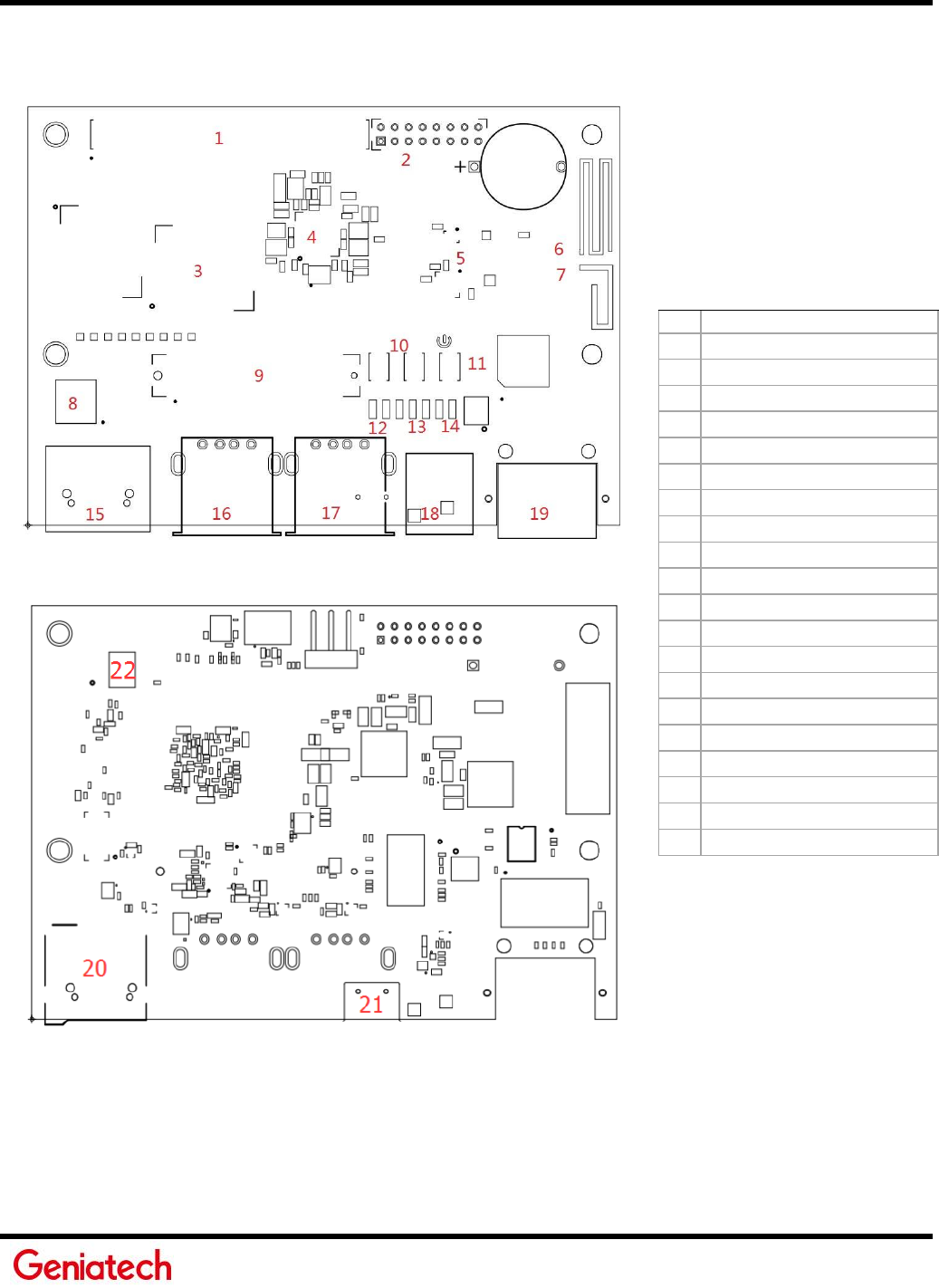
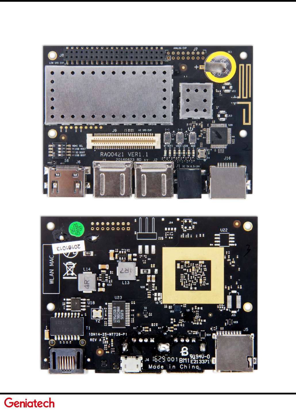
1.1
Board
overview
1. (J8) Low Speed Expansion Connector
2. (J7) Analog Expansion Connector
3. APQ8016 Snapdragon Processor
4. (U9) Power Management PMIC
5. WLAN/Bluetooth
6.
7.
Bluetooth/WLAN Antenna
8.
(S6) Boot Switches
9.
(J9) High Speed Connector
10.
(S3-4) Vol+/Vol- Buttons
11.
(S2) Power Button
12.
Bluetooth/WLAN LED’s
13.
User LED’s 1-4
14.
Ethernet LED
15.
(J6) HDMI Type A Port
16.
(J3) USB Host2 Connector
17.
(J2) USB Host1 Connector
18.
(J1) Power Jack
19.
(J16)Ethernet Connector
20.
(J5) uSD Card Socket
21.
(J4) Micro USB Type B Connector
Apple Authentication IC
7
2
What’s
in
the
Box
The box contains one DB4.

8
3
Getting
started
3.1
Prerequisites
Before you power up your DB4 for the first time you will need the following:
DB4 board.
A 96Boards compliant power supply (sold separately by Geniatech).
A HDMI or DVI LCD Monitor that supports a resolution of 1080P/30Hz.
HDMI-HDMI cable or HDMI-DVI cable to connect the board to the Monitor.
A computer keyboard with USB interface
A computer mouse with USB interface.
3.2
Starting
the
board
for
the
first
time
To start the board, follow these simple steps:
step 1. Connect the HDMI cable to the DB4 HDMI connector (marked J6) and to the LCD Monitor.
step 2. Connect the keyboard to the boards USB connector marked J3 and the mouse to the USB connector
marked J2. (It doesn’t matter which order you connect them in.
You can also connect via an external USB Hub.)
step
3.
Ensure
that
the
boot
switches
S6
are
set
to
‘0000’,
all
in
Off
position.
step 4. Connect the power supply to power connector J1.
Once you plug the power supply into a power outlet the board will start the booting process, and you should see Android
boot up.
Please note that the first boot takes several minutes due to Androids initialization. Subsequent boot times should be faster.

9
4
DB4
Overview
4.1
System
Block
diagram
4.2
Processor
The Snapdragon 410 APQ8016 is a quad 64-bit ARM Cortex-A53 MPcore Harvard Superscalar core, supports both LP-DDR2
/ LP-DDR3 SDRAM interface, Hexagon QDSP6, 13.5 MP camera input support, Adreno 306 GPU, 1080p video
encode/decode, Bluetooth 4.1, OpenGL ES 3.0, DirectX, OpenCL, Renderscript Compute, FlexRender support.
4.3
Memory
The DB4 uses a single embedded Multi Chip Package (eMCP) dual function LPDDR3/eMMC memory solution. The installed chip
provides 16Gbyte of solid state storage and 2Gbyte of LPDDR3.
The LPDDR3 is a 32bit width bus implementation interfacing directly to the APQ8016 build-in LPDDR controller.
The maximum DDR clock is 533Mhz
The eMMC is an 8bit implementation interfacing with APQ8016 SDC1 interface supporting eMMC 4.5
specifications.
4.4
MicroSDHC
The 96Boards specification calls for a microSDHC socket to be present on the board.
10
The DB4 SD slot (J5) signals are routed directly to the APQ8016 SDC2 interface. The slot is a push-push type with a
dedicated support for card detect signal (many SD slots do not have a dedicated CD pins, they use DATA3 state as the card
detected signal). The DB4 uses APQ GPIO_38 as the SD_CARD_DET_N.
4.5
Ethernet
The DB4 deployed ASIX’ USB2.0 to 10/100M Fast Ethernet Controller AX88772C solution which enables a low cost, small form
factor, and simple plug-and-play Fast Ethernet network connection capability.
4.6
WiFi/BT/RF
The 96Boards specifications calls for a WiFi (minimally 802.11g/n) and Bluetooth 4.1 (Bluetooth Low Energy)
The DB4 deployed Qualcomm’s RF chip WCN3620 (U5) solution that integrates three different wireless connectivity
technologies into a single device, the interfaces are:
WLAN compliant with IEEE 802.11 b/g/n specifications, meeting 96Boards minimal requirements for WiFi.
Bluetooth compliant with the BT specifications version 4.1 (BR/EDT + BLE), meeting the 96Boards requirements for BT
Worldwide FM radio, this interface is not part of the 96Boards mandatory specification. It is an optional addition
that has not been tested is not officially supported.
4.7
Display
Interface
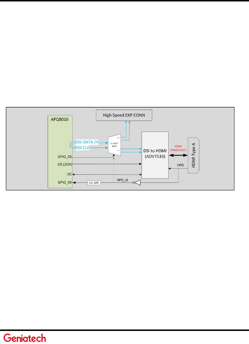
4.7.1
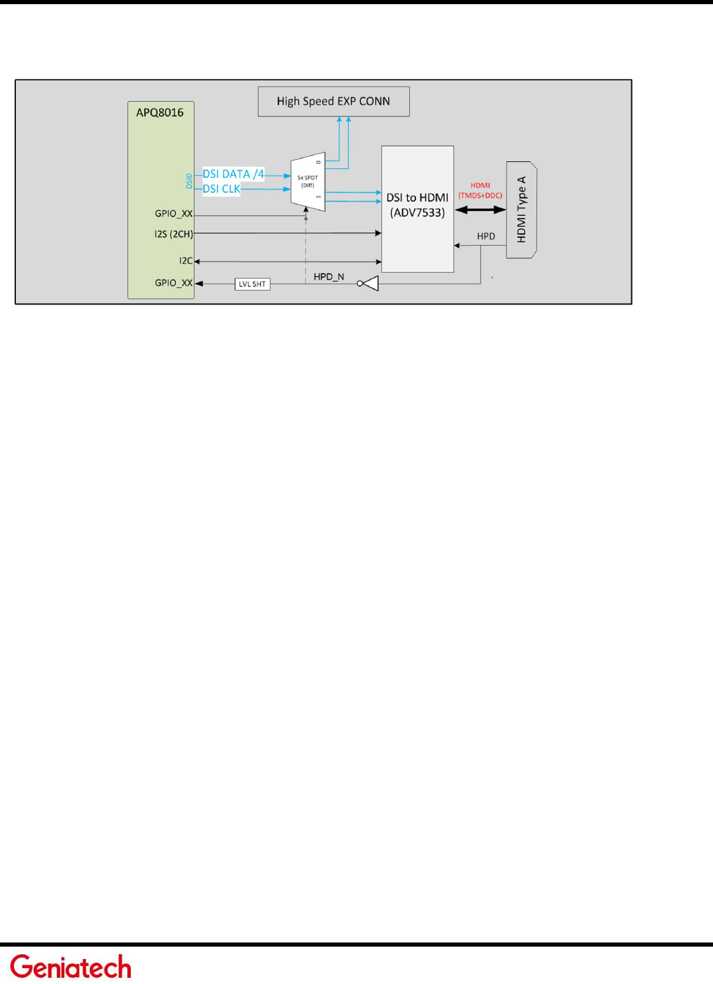
HDMI
The 96Boards specification calls for an HDMI port to be present on the board. The APQ8016 doesn’t include a built-in
HDMI interface.
The DB4 deploys the built-in MIPI-DSI 4 lanes interface as the source for the HDMI output. A peripheral DSI to
HDMI Bridge (U3, Analog Devices ADV7533) performs this task and it supports a resolution from 480i to 1080p at 30Hz.
While the ADV7533 supports automatic input video format timing detection (CEA-861E), an I2C channel from the APQ8016
allows the user to configure the operation of this bridge. It is I2C3 interface from the SoC that connects to the bridge.
This bridge supports audio as well (meeting the 96Boards requirements to provide audio via HDMI). The DB4 uses a single bit
I2S2 interface from the APQ8016 for this task.
11
Please note that the 96Boards specification calls for a MIPI-DSI interface to be routed to the High Speed Expansion connector.
Since the APQ8016 has only one MIPI-DSI interface. A muxing device (U11, FSA644UCX) is being use on the board. Only one
interface, HDMI, or the Expansion MIPI-DSI can be active at a given time. The controlling signal is named
‘DSI_SW_SEL_APQ’. When this signal is logic low, ‘0’, the MIPI-DSI is routed to the DSI-HDMI Bridge. When
‘DSI_SW_SEL_APQ’ is logic level high, ‘1’, the MIPI-DSI is routed to the High Speed Expansion connector. This design
assigned the ‘DSI_SW_SEL_APQ’ function to GPIO_32.
User can overwrite the software control by sliding switch 4 of DipSwitch S6 to the ‘ON’ position. That action forces the DSI
mux to route the MIPI-DSI to the DSI-HDMI Bridge. The overwrite option exist for the HDMI only, you cannot hardware
overwrite the mux to the High Speed Expansion connector.
4.7.2
MIPI-DSI
The 96Boards specification calls for a MIPI-DSI implementation via the High Speed Expansion Connector.
The DB4 implemented a four-lane MIPI_DSI interface meeting this requirement. More information about this
implementation can be found in chapter 6 High speed expansion connector.
4.8
Camera
Interfaces
The 96Boards specification calls for two camera interfaces.
The DB4 implements two camera interfaces, one with a four-lane MIPI_CSI interface and one with two-lane MIPI_CSI
interface, meeting this requirement. More information about this implementation can be found in chapter 6 High speed
expansion connector.
4.9
USB
Ports
4.9.1
USB-Host
ports
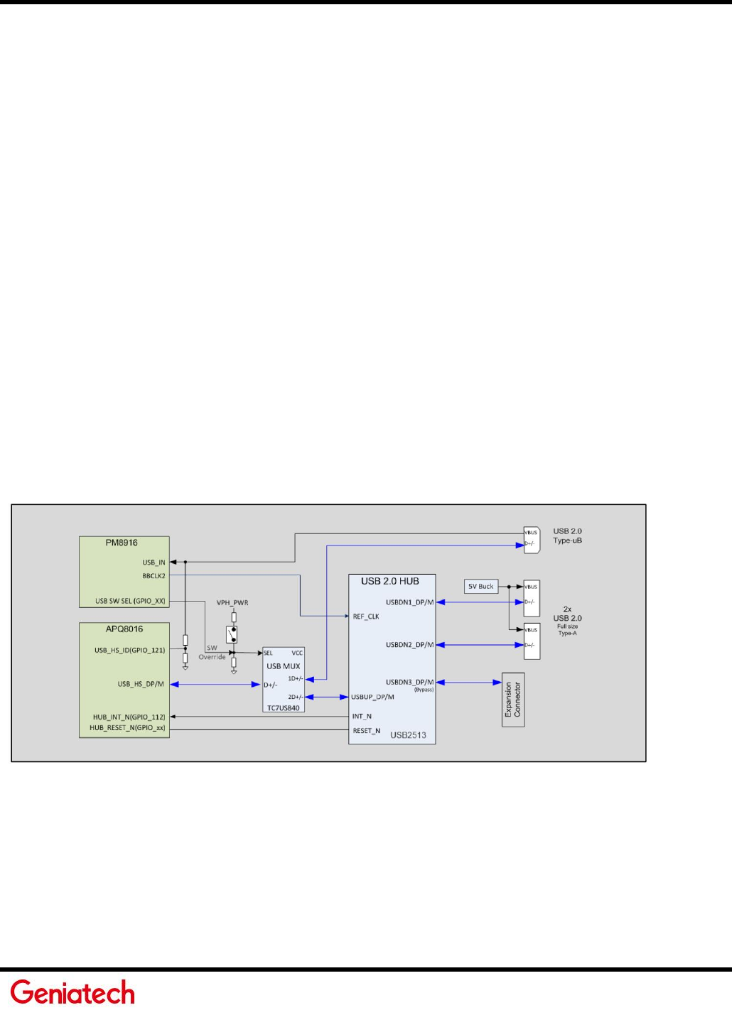
The 96Boards specification calls for three USB host ports. The APQ8016 includes a single USBOTG channel. A USB Mux, S1,
routes this single USB channel either to a USB HUB or to the MicroUSB connector (J4). The control of S1 is done via a
software controlled GPIO (USB_SW_SEL_PM, GPIO_4 from the board PMIC). When this signal is logic low, ‘0’, the USB data
lines are routed to the MicroUSB connector and the APQ8016 built-in USBOTG port is set to device mode. When
‘USB_SW_SEL_PM’ is logic level high, ‘1’, the USB data lines are routed to U10 (a 3-port USB HUB) and the APQ8016 built-
in USBOTG port is set to host mode. The user can overwrite the software control by sliding switch 3 of DipSwitch S6 to the
‘ON’ position. That action forces the USB–mux S1 to route the built-in USBOTG data lines to the USB HUB. The overwrite

12
option exists for the host mode only, you cannot hardware overwrite the mux to force device mode.
Port 1 of the USB HUB is routed to J3, a Type ‘A’ USB Host connector. A current limited controller (U4) sets the Power
Current limit to 1.18A. This port is named HOST2 in the board schematic.
Port 2 of the USB HUB is routed to J2, a Type ‘A’ USB Host connector. A current limited controller (U6) sets the Power
Current limit to 1.18A. This port is named HOST1 in the board schematic.
Port 3 of the USB HUB is routed to the High Speed Expansion connector. No current limited controller is implemented on
the board for this channel.
Please
note:
the board can work in one mode at a time, Host mode or Device mode, not both.
Please
note:
Since the APQ8016 has only a single USBOTG channel, care needs to be taken when the USB HOST function is
to be used.
Please verify that no cable is connected to the MicroUSB type B connector (and to a host on the other side of
the cable) as the hardware of the DB4 will inform software about the presence of a request to configure the
USBOTG to device mode. Depending on the software release that is used on the board, the driver may configure the USB
Mux to Device mode and none of the USB HOST ports will be connected to the SoC.
4.9.2
USB-Device
port
The 96Boards specification calls for a USB port to be implemented as an OTG port or a device port.
The DB4 implements a device port. The port is located at J4, a MicroUSB type B. If an application requires the use of
the device port, USB_SW_SEL_PM signal must be set to low ‘0’ and the user must verify that switch 3 of Dip Switch S6 is
set to the ‘OFF’ position.
Please
note:
the board can work in one mode at a time, Host mode or Device mode, not both.
4.10
Audio
The 96Boards specifications calls for a minimum of single channel audio through two interfaces, BT and
HDMI/MHL/DisplayPort..
The DB4 meets this requirement and has additional audio channels. More information about these additional channels can be
found in chapter 4.18 Additional Functionality.
4.10.1
BT
Audio
The BT implementation on the DB4 is via a MAC in the APQ8016 and an external modem, WCN3620 (U5). A two wire
interface between the SoC and the modem carries all communication including audio.
4.10.2
HDMI
Audio
A 3-wire (audio out only) I2S channel is routed directly from the APQ8016 SoC I2S interface pins to the DSI-HDMI bridge
(U3).
4.11
DC-power
and
Battery
Power
The 96Boards specification calls for power to be provided to the board in one of the following ways:
An 6.5V to 18V power from a dedicated DC jack
An 6.5V to 18V power from the SYS_DCIN pins on the Low Speed Expansion Connector
A USB Type C port at 5V
Please see section 9.1 for detailed information on DB4 implementation of DC Power

13
4.12
Measurements
The 96Boards specification calls for support for measuring power consumptions of the board.
Please see section 8.6 for detailed information on DB4 power measurement implementation.
4.13
Buttons
The 96Boards specification calls for the present of two buttons, a Power on/sleep button and a Reset button.
The DB4 meets these requirements.
Please see section 10 for detailed information on the buttons of the DB4.
4.14
External
Fan
connection
The 96Boards specification calls for support for an external fan. That can be achieved by using the 5V or the SYS_DCIN,
both present on the Low Speed Expansion connector.
4.15
UART
The 96Boards specification calls for support for one SoC UART and an optional second UART both to be routed to the Low
Speed Expansion Connector.
The DB4 meets these requirements and additionally routes UART0 Tx/Rx lines to an on-board connector (J15). If the user wants
to use this on-board UART, J15 needs to be soldered to the board as well as R173 and R174 (0 ohm 0201).
4.16
JTAG
The 96Boards specification does not call for a dedicated JTAG connector. However the DB4 has JTAG and UART
signals routed to J15. The J15 connector does not have a standard JTAG connector pitch and is not populated on the board.
4.17
System
and
user
LEDs
The 96Boards specifications calls for six LEDs to be implemented on the board.
The specification defines the LEDs color
and mechanical location on the board.
Three
activity
LEDs:
• WiFi activity LED – DB4 drives this Yellow LED via MPP_2, an IO from the PMIC.
• BT activity LED – DB4 drives this Blue LED via MPP_3, an IO from the PMIC.
• Etherent activity LED – Ax88772C drives this Green LED.
Four
User-LED’s:
The four user LEDs are surface mount Green in
0603 size located next to the two USB type A connector and labeled ‘USER
LEDS 4 3 2 1’. The DB4 drives two LEDs from the SoC GPIO, APQ GPIO_21 and APQ GPIO_120. The other two User
LEDs are driven by the PMIC via PM GPIO_1 and PM GPIO_2.
4.18
Expansion
Connector
The 96Boards specification calls for two Expansion Connectors, a Low Speed and a High Speed.
The DB4 meets this requirement, please review section 6.0 for detailed information regarding the Low Speed Expansion
Connector and section 7.0 for detailed information regarding the High Speed Expansion Connector.

14
4.19
Additional
Functionality
The 96Boards specifications allows for additional functionality provided that all mandatory functionality is available and
there is no impact on the physical footprint specifications including height and do not prevent the use of the 96Boards CE
low speed and high speed expansion facilities.
The DB4 implements a few additional functions, which are listed in the following sub-chapters.
4.19.1
On
Board
Analog
Microphone
Information on the on board microphone can be found in section 8.2.
4.19.2
Analog
Connector
Detailed information on the analog connector is provided in section 8.0.
15
5
Low
speed
Expansion
connector
The following tables show the Low Speed Expansion Connector pin out:
PIN 96Boards
Signals
DB4
Signals
Note
1
3
5
7
9
11
13
15
17
19
21
23
25
27
29
31
33
35
37
39
GND
UART0_CTS
UART0_TxD
UART0_RxD
UART0_RTS
UART1_TxD
UART1_RxD
I2C0_SCL
I2C0_SDA
I2C1_SCL
I2C1_SDA
GPIO-A
GPIO-C
GPIO-E
GPIO-G
GPIO-I
GPIO-K
+1V8
+5V
GND
GND
UART0_CTS_N (APQ GPIO_2)
UART0_TX (APQ GPIO_0)
UART0_RX (APQ GPIO_1)
UART0_RTS_N (APQ GPIO_3)
UART1_TX (APQ GPIO_4)
UART1_RX (APQ GPIO_5)
I2C0_SCL (APQ GPIO_7)
I2C0_SDA (APQ GPIO_6)
I2C1_SCL (APQ GPIO_23)
I2C1_SDA (APQ GPIO_22)
LS_EXP_GPIO_A (APQ GPIO_36) (APQ INT)
LS_EXP_GPIO_C (APQ GPIO_13) (TS_INT_N)
LS_EXP_GPIO_E (APQ GPIO_115)
(GYRO_ACCL_INT_N)
LS_EXP_GPIO_G (APQ GPIO_24) (DSI_VSYNC)
LS_EXP_GPIO_I (APQ GPIO_35) (CSI0_RST)
LS_EXP_GPIO_K (APQ GPIO_28) (CSI1_RST)
LS_EXP_1P8
SYS_5P0
GND
16
PIN 96Boards Signals DB4 Signals Note
2
4
6
8
10
GND GND
12
14
16
18
20
22
24
26
28
30
32
34
36
38
40
GND
PWR_BTN_N
RST_BTN_N
SPI0_SCLK
SPI0_DIN
SPI0_CS
SPI0_DOUT
PCM_FS
PCM_CLK
PCM_DO
PCM_DI
GPIO-B
GPIO-D
GPIO-F
GPIO-H
GPIO-J
GPIO-L
SYS_DCIN
SYC_DCIN
GND
GND
PHONE_ON_N
PM_RESIN_N
SPI0_CLK (APQ GPIO_19)
SPI0_MISO (APQ GPIO_17)
SPI0_CS_N (APQ GPIO_18)
SPI0_MOSI (APQ GPIO_16)
LS_EXP_MI2S_WS (APQ GPIO_110)
LS_EXP_MI2S_SCK (APQ GPIO_113) (ALPS_INT)
LS_EXP_MI2S_DATA0 (APQ GPIO_114)
N.C.
LS_EXP_GPIO_B (APQ GPIO_12) (TS_RST_N)
LS_EXP_GPIO_D (APQ GPIO_69) (MAG_INT)
LS_EXP_GPIO_F (PM_MPP_4) (DSI_BLCTRL))
LS_EXP_GPIO_H (APQ GPIO_25) (DSI_RST)
LS_EXP_GPIO_J (APQ GPIO_34) (CSI0_PWDN)
LS_EXP_GPIO_L (APQ GPIO_33) (CSI1_PWDN)
SYS_DCIN
SYS_DCIN
GND
I2S
only
supports
audio
out
Borrowed
GPIO
from
PMIC

17
5.1
UART
{0/1}
The 96Boards specifications calls for a 4-wire UART implementation, UART0 and an optimal second 2-wire UART, UART1 on
the Low Speed Expansion Connector.
The DB4 implements UART0 as a 4-wire UART that connects directly to the APQ8016 SoC. These signals are driven
at 1.8V.
The DB4 implements UART1 as a 2-wire UART that connects directly to the APQ8016 SoC. These signals are driven
at 1.8V.
5.2
I2C
{0/1}
The 96Boards specification calls for two I2C interfaces to be implemented on the Low Speed Expansion Connector.
The DB4 implements both interfaces, I2C0 and I2C1 that connects directly to the APQ8016SoC. A 2K resistor is
provided as pull-up for each of the I2C lines per the I2C specifications, these pull-ups are connected to the 1.8V voltage
rail.
5.3
GPIO
{A-L}
The 96Boards specifications calls for 12 GPIO lines to be implemented on the Low Speed Expansion Connector.
Some of
these GPIOs may support alternate functions for DSI/CSI control
The DB4 implements this requirement.
11 GPIOs are routed to the APQ8016 SoC and one GPIO is connected to the
on-board PMIC.
GPIO A - Connects to GPIO_36 of APQ8016 SoC, can serves as AQP_INT supporting the 96Boards requirements to
create a wake-up event for the SoC. It is a 1.8V signal
GPIO B - Connects to GPIO_12 of APQ8016 SoC. It is a 1.8V signal
GPIO C - Connects to GPIO_13 of APQ8016 SoC. It is a 1.8V signal. Can be configured to be an IRQ line
GPIO D - Connects to GPIO_69 of APQ8016 SoC. It is a 1.8V signal. Can be configured to be an IRQ line
GPIO E - Connects to GPIO_115 of APQ8016 SoC. It is a 1.8V signal. Can be configured to be an IRQ line
GPIO F - Connects to MPP_4 of PM8916 PMIC. It is a 1.8V signal. Can be configured to be the DSI backlight control
GPIO G - Connects to GPIO_24 of APQ8016 SoC. It is a 1.8V signal. Can be configured to be DSI VSYNC signal.
GPIO H - Connects to GPIO_25 of APQ8016 SoC. It is a 1.8V signal. Can be configured to be a DSI_RST signal.
GPIO I - Connects to GPIO_35 of APQ8016 SoC. It is a 1.8V signal. Can be configured to be a CSI0_RST signal.
GPIO J - Connects to GPIO_34 of APQ8016 SoC. It is a 1.8V signal. Can be configured to be a CSI0_PWDN signal.
GPIO K - Connects to GPIO_28 of APQ8016 SoC. It is a 1.8V signal. Can be configured to be a CSI1_RST signal.
GPIO L - Connects to GPIO_33 of APQ8016 SoC. It is a 1.8V signal. Can be configured to be a CSI1_PWDN signal.
5.4
SPI
0
The 96Boards specification calls for one SPI bus master to be provided on the Low Speed Expansion Connector.
The DB4 implements a full SPI master with 4 wires, CLK, CS, MOSI and MISO all connect directly to the APQ8016
SoC. These signals are driven at 1.8V.
5.5
PCM/I2S
The 96Boards specification calls for one PCM/I2S bus to be provided on the Low Speed Expansion Connector. The CLK, FS
and DO signals are required while the DI is optional.
The DB4 implements a PCM/I2S with 3 wires, CLK, FS and DO, the optional DI signal is not implemented on the DB4 board.
The
I2S signals are connected directly to the APQ8016 SoC. These signals are driven at 1.8V.

18
5.6
Power
and
Reset
The 96Boards specification calls for a signal on the Low Speed Expansion Connector that can power on/off the board and a
signal that serves as a board reset signal.
The DB4 routes the PWR_BTN_N (named PHONE_ON_N on DB4 schematic) signal to the KYPDPWR_N pin of the PM8916 PMIC.
This signal is driven by S2 as well, the on-board power on push-button switch.
Please note that the push
button only provides an On/Sleep function and not OFF functionality.
A mezzanine implementation of this signals should not drive it with any voltage, the only allowed operation is to force it to
GND to start the board from a sleep mode. A board shutdown will occur when this signal is held to ground for more than
15 seconds (based on the current Android release).
The DB4 routes the RST_BTN_N (named PM_RESIN_N on DB4 schematic) signal to the RESIN_N pin of the PM8916 PMIC. This
signal is driven by S4, the on-board reset switch. This signals is a dual purpose, any press lasting less than 10 seconds serves as
Volume Down or Zoom out, a press longer than 10 seconds will reset the board.
5.7
Power
Supplies
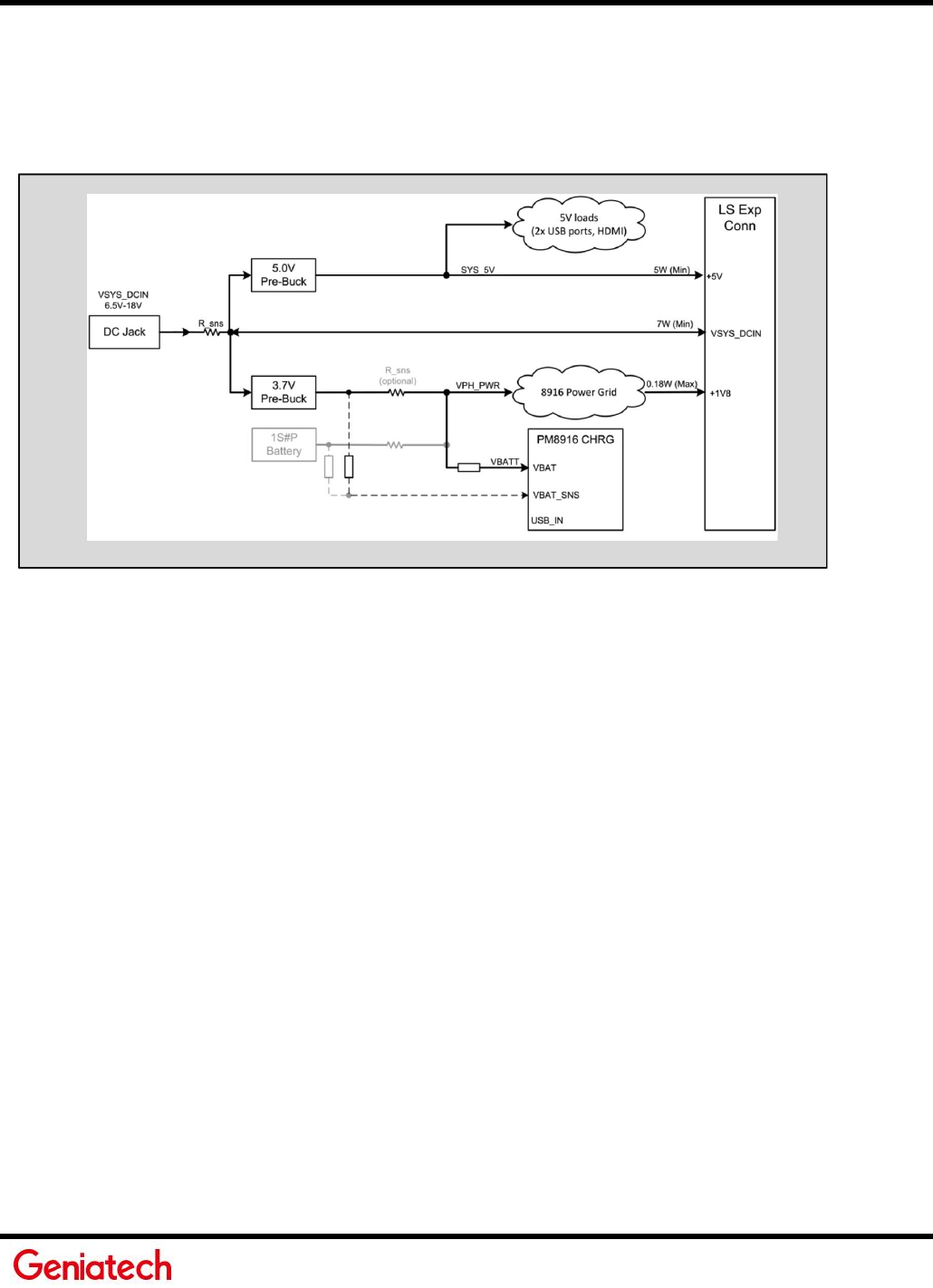
The 96Boards specification calls for three power rails to be present on the Low Speed Expansion Connector:
+1.8V : Max of 100mA
+5V : Able to provide a minimum of 5W of power (1A).
SYS_DCIN
: 9-18V input with enough current to support all the board functions or the output DCIN from on-
board DC Connector able to provide a minimum of 7W of power.
The DB4 supports these requirements as follows:
+1.8V : Driven by two PMIC LDOs, LDO15 and LDO16, each can provide 55mA. The PM8916 allows connecting the two
LDOs in parallel to provide 110mA on a 1.8V rail which meets the 96Boards requirement.
+5V : Driven by the 4A 5.0V buck switcher (U13). This buck switcher powers both USB limit current devices (each at
1.18A max).
The remaining capacity provides a max current of 1.64A to the Low Speed Expansion Connector, for a total of
8.2W which meets the 96Boards requirements.
SYS_DCIN: Can serves as the board’s main power source or can receive power from the board.
19
6
High
speed
expansion
connector
The following table shows the High Speed Expansion Connector pin out:
PIN
96Boards
Signals
DB4
Signals
Note
1
3
5
7
9
11
13
15
17
19
21
23
25
27
29
31
33
35
37
39
41
43
45
47
49
51
53
55
57
59
SD_DAT0/SPI1_DOUT
SD_DAT1
SD_DAT2
SD_DAT3/SPI1_CS
SD_SCLK/SPI1_SCLK
SD_CMD/SPI1_DIN
GND
CLK0/CSI0_MCLK
CLK1/CSI1_MCLK
GND
DSI_CLK+
DSI_CLK-
GND
DSI_D0+
DSI_D0-
GND
DSI_D1+
DSI_D1-
GND
DSI_D2+
DSI_D2-
GND
DSI_D3+
DSI_D3-
GND
USB_D+
USB_D-
GND
HSIC_STR
HSIC_DATA
SPI1_MOSI (APQ GPIO_8)
N.C.
N.C.
SPI1_CS_N (APQ GPIO_10)
SPI1_CLK (APQ GPIO_11)
SPI1_MISO (APQ GPIO_9)
GND
CSI0_MCLK (APQ GPIO_26)
CSI1_MCLK (APQ GPIO_27)
GND
MIPI_DSI0_CLK_P_EXP_CONN
MIPI_DSI0_CLK_M_EXP_CONN
GND
MIPI_DSI0_DATA0_P_EXP_CONN
MIPI_DSI0_DATA0_M_EXP_CONN
GND
MIPI_DSI0_DATA1_P_EXP_CONN
MIPI_DSI0_DATA1_M_EXP_CONN
GND
MIPI_DSI0_DATA2_P_EXP_CONN
MIPI_DSI0_DATA2_M_EXP_CONN
GND
MIPI_DSI0_DATA3_P_EXP_CONN
MIPI_DSI0_DATA3_M_EXP_CONN
GND
USB_HS_D_P_EXP
USB_HS_D_M_EXP
GND
N.C.
N.C.
This
is
a
SPI
implementation.
not
an
SD
interface
No
HSIC
implementation
20
PIN
96Boards
Signals
DB4
Signals
Note
2
4
6
8
10
12
14
16
18
20
22
24
26
28
30
32
34
36
38
40
42
44
46
48
50
52
54
56
58
60
CSI0_C+
CSI0_C-
GND
CSI0_D0+
CSI0_D0-
GND
CSI0_D1+
CCSI0_D1-
GND
CSI0_D2+
CSI0_D2-
GND
CSI0_D3+
CSI0_D3
GND
I2C2_SCL
I2C2_SCL
I2C3_SDA
I2C3_SDA
GND
CSI1_D0+
CSI1_D0-
GND
CSI1_D1+
CSI1_D1-
GND
CSI1_C+
CSI1_C-
GND
RESERVED
MIPI_CSI0_CLK_P
MIPI_CSI0_CLK_M
GND
MIPI_CSI0_DATA0_P
MIPI_CSI0_DATA0_M
GND
MIPI_CSI0_DATA1_P
MIPI_CSI0_DATA1_M
GND
MIPI_CSI0_DATA2_P
MIPI_CSI0_DATA2_M
GND
MIPI_CSI0_DATA3_P
MIPI_CSI0_DATA3_M
GND
I2C2_SCL (APQ GPIO_30)
I2C2_SDA (APQ GPIO_29)
I2C3_SCL (APQ GPIO_15)
I2C3_SDA (APQ GPIO_14)
GND
MIPI_CSI1_DATA0_P
MIPI_CSI1_DATA0_M
GND
MIPI_CSI1_DATA1_P
MIPI_CSI1_DATA1_M
GND
MIPI_CSI1_CLK_P
MIPI_CSI1_CLK_M
GND
N.C.
R61
&
R62
need
to
be
Installed
to
enable
I2C3
21
6.1
MIPI
DSI
0
The 96Boards specification calls for a MIPI-DSI to be present on the High Speed Expansion Connector. A minimum of one
lane is required and up to four lanes can be accommodated on the connector.
The DB4 implementation supports a full four lane MIPI-DSI interface that is routed to the High Speed Expansion
Connector. Since the APQ8016 has only single MIPI-DSI interface and it may be used to drive the DSI-HDMI Bridge, DSI
muxing is required.
A muxing device, U11 (FSA644UCK) is used on the board. Only one interface, HDMI, or the Expansion MIPI-DSI can be
active at a given time. The controlling signal is named ‘DSI_SW_SEL_APQ’. When this signal is logic low, ‘0’, the MIPI-DSI is
routed to the DSI-HDMI Bridge.
When ‘DSI_SW_SEL_APQ’ is logic level high, ‘1’, the MIPI-DSI is routed to the High Speed Expansion connector. This design
assigned the ‘DSI_SW_SEL_APQ’ function to GPIO_32.
The user can override the software control by sliding switch 4 of DipSwitch S6 to the ‘ON’ position. That action forces the
DSI mux to route the MIPI-DSI to the DSI-HDMI Bridge. The override option exists for HDMI only.
You cannot force the mux
to the High Speed Expansion connector.
While hardware forces the ESI Mux to the HDMI, software must configure the
HDMI bridge for proper functionality.
Please
note
: If configuring the board to use the MIPI-DSI is done via software, the user must verify the switch 4 of
DipSwitch S6 is set to the ‘off’ position
6.2
MIPI
CSI
{0/1}
The 96Boards specification calls for two MIPI-CSI interfaces to be present on the High Speed Expansion Connector. Both
interfaces are optional. CSI0 interface can be up to four lanes while CSI1 is up to two lanes.
The current DB4 implementation supports a full four lane MIPI-CSI interface on CSI0 and two lanes of MIPI-CSI on
CSI1. All MIPI-CSI signals are routed directly to/from the APQ8016.
6.3
I2C
{2/3}
The 96Boards specification calls for two I2C interfaces to be present on the High Speed Expansion Connector. Both
interfaces are optional unless a MIPI-CSI interface has been implemented. Then an I2C interface shall be implemented.
The current DB4 implementation supports two MIPI-CSI interfaces and therefore must support two I2C interfaces.
For MIPI-CSI0 the companion I2C2 is routed directly from the APQ8016. For MIPI-CSI1, the companion I2C is I2C3.
Note: You will need to add R61 and R62, 0 ohm 0201 resistors, to the board to support the routing of I2C3 interface to the
High Speed Expansion Connector. Both interfaces, I2C2 and I2C3 have an on-board 2K pull-up resistors pulled-up to the

22
1.8V voltage rail.
6.4
HSIC
The 96Boards specification calls for an optional MIPI-HSIC interface to be present on the High Speed Expansion Connector.
The DB4 implementation doesn’t support this optional requirement.
6.5
Reserved
The 96Boards specification calls for a 10K pull-up to 1.8V to be connected to pin 60 of the High Speed Expansion
Connector.
The current DB4 implementation does not support this requirement.
This issue will be addressed on a future
revision of the DB4.
6.6
SD/SPI
The 96Boards specification calls for an SD interface or a SPI port to be part of the High Speed Expansion Connector.
The DB4 implements a full SPI master with 4 wires (96Boards SPI Configuration), CLK, CS, MOSI and MISO all
connect directly to the APQ8016 SoC. These signals are driven at 1.8V.
6.7
Clocks
The 96Boards specification calls for one or two programmable clock interfaces to be provided on the High Speed Expansion
Connector. These clocks may have a secondary function of being CSI0_MCLK and CSI1_MCLK. If these clocks can’t be
supported by the SoC than an alternative GPIO or No-Connect is allowed by the specifications.
The DB4 implements two CSI clocks, CSI0_MCLK via APQ GPIO_26 and CSI1_MCLK via APQ GPIO_27. These signals
are driven at 1.8V.
6.8
USB
The 96Boards specification calls for a USB Data line interface to be present on the High Speed Expansion Connector.
The DB4 implements this requirements by routing USB channel 3 from the USB HUB to the High Speed Expansion
Connector.
23
7
Analog
Expansion
Connector
7.1
Speaker
The speaker signals are routed from the PM8916 PMIC built-in Audio CODEC, the two signals are:
SKPR_DRV_P
- Class-D speaker amplifier output+
SKPR_DRV_M
- Class-D speaker amplifier output-
7.2
Mic
The microphone signals are rounded to the PM8916 PMIC Built-In CODEC, the three signals are:
MIC2_IN - Headset mic
MIC3_IN - Second mic, please note that the first microphone input, MIC1_IN is routed from an on-board
analog microphone (not installed on current DB4 builds)
MIC_BIAS1 - Ground reference for PMIC bias
7.3
Headset
The headset signals are rounded from the PM8916 PMIC Built-In CODEC, one signal is routed from the connector to the
CODEC, the singles are:
HPH_R - Headphone PA right channel output
HPH_L - Headphone PA left channel output
HPH_REF - Headphone PA ground sensing
HS_DET - Headset detection
7.4
FM
Antenna
PIN Function Connect to Note
1
2
3
4
5
6
7
8
9
1
0
11
12
13
14
15
16
SPKR_OUT_P
SPKR_OUT_M
VPH_PWR
GND
GND_CFILT
CDC_MIC2_P
CDC_MIC3_P
CDC_HPH_R
CDC_HPH_REF
CDC_HPH_L
CDC_HS_DET
CDC_MIC_BIAS1
N.C.
N.C.
N.C.
FM_RX_ANT
N.C.
PM8916 Audio signal CDC_SPKDRV_P
PM8916 Audio signal CDC_SPKDRV_M
A 3.7V from U12 buck switcher
PM8916 Audio signal CDC_GND_CFILT
PM8916 Audio signal CDC_IN2_P
PM8916 Audio signal CDC_IN3_P
PM8916 Audio signal CDC_HPH_R
PM8916 Audio signal CDC_HPH_REF
PM8916 Audio signal CDC_HPH_L
PM8916 Audio signal CDC_HS_DET
PM8916 Audio signal CDC_MIC_BIAS1
WCN3620 RF signal FM_HS_RX
Datasheet pin SPKR_DRV_P
Datasheet pin SPKR_DRV_M
Datasheet pin MIC2_IN
Datasheet pin MIC3_IN

24
The FM_RX_ANT signal is the path for the FM antenna to reach the WCN3620 (u5), an integrated three different
connectivity technologies device:
WLAN IEE802.11 b/g/n
BT 4.0 (BR/EDR/BLE)
Worldwide FM radio
25
8
Power
management
The 96Boards specification defines how power arrives to the board and few supplies that the board needs to provide. The
on board power requirement for each 96Boards implementation depends on the SoC and the set of peripherals that are
specific to that implementation.
The DB4 uses two buck regulators, U13 and U12. U13 takes the power in to the board and generates 5V at 4A. This
voltage feeds the USB HOST power limit switches and provides power to the Low Speed Expansion port. U12 takes the
power in to the board and generates 3.7V at 4A. This voltage serves as the power in voltage to the on-board PMIC,
PM8916 (U9). The PM8916 can generate 25 different voltage rails.
8.1
DC
Power
Input
The 96Boards specification calls for a power to be provided to the board in one of the following ways:
An 8V to 18V power from a dedicated DC jack.
The DB4 supports this requirement through the use of J1, ‘SYS_DCIN’ power connector.
Please
note:
the SYS_DCIN can be as low as 6.5V on the DB4.
An 8V to 18V power from the SYS_DCIN pins on the Low Speed Expansion Connector.
Please
note:
the SYS_DCIN can be as low as 6.5V on the DB4.
The DB4 supports incoming power through this connector.
A USB Type C port at 5V.
Please
note:
The
DB4
does
not
implement
a
USB
Type
C
port
and
therefore
cannot
be
powered
over
USB.
8.2
Power
Source
Selection
Following the information in section 9.1, the DB4 has only two sources for board incoming power. The 96Boards
specification calls for only one power source to be applied to the board at any given time. Following this requirement,
the
user
of
the
DB4
should
never
apply
power
to
the
board
from
J1
and
the
Low
Speed
Expansion
connector
at
the

26
same
time
. There is no active or passive mechanism on the DB4 to prioritize one source over the other.
8.3
Power
Consumption
The power consumption of DB4 will be less than 5W.
8.4 Power Sequencing
Upon applying power to the DB4 (either one of the two sources), both buck regulators will be enabled and will start
regulating their target voltages. When the output of U12 is on, it will power the on-board PMIC, the PM8916. This PMIC
has four buck regulators, one boost regulator and 20 LDOs. The sequencing of all power rails is set within the PM8916
configuration scheme during the production of this part. The user has no access to alter, modify or change the PMIC power
up sequencing.
8.5
Voltage
Rails
Please see section 10 for detailed list of the power rails on the DB4.
8.6
Power
Measurements
The 96Boards specification calls for a minimum of one current sense resistor to be placed on the board permitting a basic
power measurement functions.
The DB4 implements two different power measurements.
8.6.1
Power-In
measurement
A 0.1ohm resistor is placed inline to the SYS_DCIN power line coming from J1 (please note that this power in measurement
only works for SYS_DCIN from J1, it will not measure SYS_DCIN applied from the Low Speed Expansion Connector). Placing
a probe over this resistor will provide a voltage measurement of the voltage drop across the resistor. Dividing this
measurement by 0.1 will give you the amount of the current flowing into the board. The board provides a means to use
ARM Energy probe for this measurement, please verify that JP3 and JP4 are each shorted and J10 is soldered to the board
to take advantage of this probe.
8.6.2
PMIC
Power-In
measurement
A 0.1ohm resistor should replace the existing inline 0 ohm resistor on VPH_PWR line, the output of U12 buck regulator
that feeds the PMIC. Placing a probe over this resistor will provide a voltage measurement of the voltage drop across the
resistor. Dividing this value by 0.1 will give you the amount of the current flowing into the PMIC. The board provides a
means to use an ARM Energy probe for this measurement, the following steps are requires to get this probe measuring this
rail:
1.
Remove
R122
and
R123
from
the
board
to
prevent
a
short
between
SYS_DCIN
and
VPH_PWR
2.
J10 needs to be soldered to the board.
3.
R124 and R125, 0 ohm 0201 resistors, need to be soldered to the board.

27
9
Buttons
and
status
LED’s
9.1
Buttons
9.1.1
Volume
up
The Volume UP button is used to control the output speaker volume of the DB4.
9.1.2
Volume
down
The Volume Down button is used to control the output speaker volume of the DB4.
9.1.3
Power
Button
The push-button S2 serves as the power-on/sleep button. Upon applying power to the board, the boot process will start.
Once the board is running you can turn power-off by pressing the power button for more than x seconds. If the board is in
a sleep mode, pressing the power bottom for more than 3 seconds will wake up the board.
9.1.4
Reset
Button
The on-board S4 push-button has two functions, it serves as a reset button and as a Volume/Zoom- button.
A button press with duration of less than 10 second will be interpreted by software as a volume down or zoom out
request. Duration of more than 10 seconds will cause a system reset.
9.2
LED’s
There are two status LEDs and four User LEDs on the DB4. The Status LEDs report the status of the Bluetooth and
Wi-Fi devices onboard. The user LEDs are driven by the SoC directly.
9.2.1
User
LED
1-4
The four user LEDs are surface mount Green LED, 0603 size, located next to the two USB type A connector and labeled
‘USER LEDS 4 3 2 1’.
9.2.2
Bluetooth
status
The BT LED on the DB4 is located next to the USBOTG connector; this LED reflects the status of the Bluetooth
device.
9.2.3
WiFi
status
The WIFI LED on the DB4 is located beside the BT LED, this LED reflects the status of the Wi-Fi device.
9.2.4 Ethernet status
The Ethernet LED on the DB4 is located beside the User LED, this LED reflects the status of the Ethernet status.

28
10
Boot
configuration
There is a 4 switch DipSwitch marked S6 located at the bottom side of the DB4. For normal operation all four
switched need to be set to the ‘off’ position.
Switch 1, ‘USB BOOT’, when set to ‘on’ position, will force boot over USB connection with a PC. This is only required for
eMMC boot image upgrade. Please review the proper OS User Guide for more information on this process.
Switch 2, ‘SD BOOT’, when set to ‘on’ position, will force the SD, J5, to serve as the boot source for the DB4 when
set. You can use uSD as the main boot source or it can serve as a method for eMMC boot image upgrade. Please review the
proper OS User Guide for more information on this process.
Switch 3, ‘USB HOST’, is described in section 5.8.
This switch in not part of the boot configuration.
Switch 4, ‘HDMI SEL’, is described in section 5.6.1. This switch is not part of the boot configuration.
FCC warning
This equipment has been tested and found to comply with the limits for a Class B digital device, pursuant to Part 15 of the FCC
rules. These limits are designed to provide reasonable protection against harmful interference in a residential installation. This
equipment generates, uses and can radiate radio frequency energy and, if not installed and used in accordance with the
instructions, may cause harmful interference to radio or television reception, which can be determined by turning the equipment
off and on.
The user is encouraged to try to correct the interference by one or more of the following measures.
- Reorient or relocate the receiving antenna.
- Increase the separation between the equipment and receiver.
- Consult the dealer or an experienced radio/TV technician for help.
- This class B digital product meets all requirements of the Canadian Interference - Causing Equipment Regulations.
This equipment complies with FCC radiation exposure limits set forth for an uncontrolled environment. This equipment should be
installed and operated with minimum distance 20cm between the radiator & your body.
You are cautioned that changes or modifications not expressly approved by the party responsible for compliance could void your
authority to operate the equipment.
The distance between user and products should be no less than 20cm