Getac Technology PS336R RFID Module User Manual
Getac Technology Corporation RFID Module
User Manual

TRF7960
TRF7961
www.ti.com
SLOU186F–AUGUST 2006–REVISED AUGUST 2010
MULTI-STANDARD FULLY INTEGRATED 13.56-MHZ RFID
ANALOG FRONT END AND DATA-FRAMING READER SYSTEM
Check for Samples: TRF7960,TRF7961
1 Introduction
1.1 Features
12
•Completely Integrated Protocol Handling •Parallel 8-Bit or Serial 4-Pin SPI Interface With
MCU Using 12-Byte FIFO
•Separate Internal High-PSRR Power Supplies
for Analog, Digital, and PA Sections Provide •Ultra-Small 32-Pin QFN Package
Noise Isolation for Superior Read Range and (5 mm ×5 mm)
Reliability •Available Tools
•Dual Receiver Inputs With AM and PM –Reference Design/EVM With Development
Demodulation to Minimize Communication Software
Holes –Source Code Available for MSP430
•Receiver AM and PM RSSI
•Reader-to-Reader Anti-Collision 1.2 APPLICATIONS
•High Integration Reduces Total BOM and Board •Secure Access Control
Area •Product Authentication
–Single External 13.56-MHz Crystal Oscillator –Printer Ink Cartridges
–MCU-Selectable Clock-Frequency Output of
RF, RF/2, or RF/4 –Blood Glucose Monitors
–Adjustable 20-mA, High-PSRR LDO for •Contactless Payment Systems
Powering External MCU •Medical Systems
•Easy to Use With High Flexibility
–Auto-Configured Default Modes for Each
Supported ISO Protocol
–12 User-Programmable Registers
–Selectable Receiver Gain and AGC
–Programmable Output Power
(100 mW or 200 mW)
–Adjustable ASK Modulation Range
(8% to 30%)
–Built-In Receiver Band-Pass Filter With
User-Selectable Corner Frequencies
•Wide Operating Voltage Range of 2.7 V to 5.5 V
•Ultra-Low-Power Modes
–Power Down <1μA
–Standby 120 μA
–Active (Rx only) 10 mA
1.3 Description
The TRF7960/61 is an integrated analog front end and data-framing system for a 13.56-MHz RFID reader
system. Built-in programming options make it suitable for a wide range of applications for proximity and
vicinity RFID systems.
The reader is configured by selecting the desired protocol in the control registers. Direct access to all
control registers allows fine tuning of various reader parameters as needed.
1
Please be aware that an important notice concerning availability, standard warranty, and use in critical applications of Texas
Instruments semiconductor products and disclaimers thereto appears at the end of this data sheet.
2Tag-it is a trademark of Texas Instruments Incorporated.
PRODUCTION DATA information is current as of publication date. Copyright ©2006–2010, Texas Instruments Incorporated
Products conform to specifications per the terms of the Texas
Instruments standard warranty. Production processing does not
necessarily include testing of all parameters.

TRF7960
TRF7961
SLOU186F–AUGUST 2006–REVISED AUGUST 2010
www.ti.com
Table 1-1. PRODUCT SELECTION TABLE
PROTOCOLS
DEVICE ISO14443A/B ISO15693 Tag-it™
ISO18000-3
106 kbps 212 kbps 424 kbps 848 kbps
TRF7960 √√√√√√
TRF7961 √ √
2Introduction Copyright ©2006–2010, Texas Instruments Incorporated
Submit Documentation Feedback
focus.ti.com: TRF7960 TRF7961
TRF7960
TRF7961
www.ti.com
SLOU186F–AUGUST 2006–REVISED AUGUST 2010
1 Introduction .............................................. 14.4 ELECTRICAL CHARACTERISTICS ................. 8
4.5 Application Schematic for the TRF796x EVM
1.1 Features .............................................. 1
(Parallel Mode) ....................................... 9
1.2 APPLICATIONS ...................................... 14.6 Application Schematic for the TRF796x EVM (SPI
1.3 Description ........................................... 1Mode) ............................................... 10
2 Description (continued) ................................ 45 System Description ................................... 11
3 Physical Characteristics ............................... 55.1 Power Supplies ..................................... 11
3.1 Terminal Functions ................................... 55.2 Receiver –Analog Section ......................... 17
5.3 Register Descriptions ............................... 24
3.2 PACKAGING/ORDERING INFORMATION .......... 6
5.4 Direct Commands From MCU to Reader ........... 34
4 ELECTRICAL SPECIFICATIONS ..................... 7
5.5 Reader Communication Interface .................. 36
4.1 ABSOLUTE MAXIMUM RATINGS .................. 7
5.6 Parallel Interface Communication .................. 38
4.2 DISSIPATION RATINGS TABLE .................... 75.7 Serial Interface Communication .................... 40
4.3 RECOMMENDED OPERATING CONDITIONS ..... 75.8 External Power Amplifier Application ............... 44
Copyright ©2006–2010, Texas Instruments Incorporated Contents 3
Submit Documentation Feedback
focus.ti.com: TRF7960 TRF7961
8(Parallel)
3(SPI)
Z – Matching
Circuit
Tx_Out
Rx_IN1
Rx_IN2
VDD_X
VDD_I/O
SYS_CLK
DATA_CLK
VDD
TRF796x MSP430
Xtal
13.56MHz
IRQ
XtalIn
XtalOut
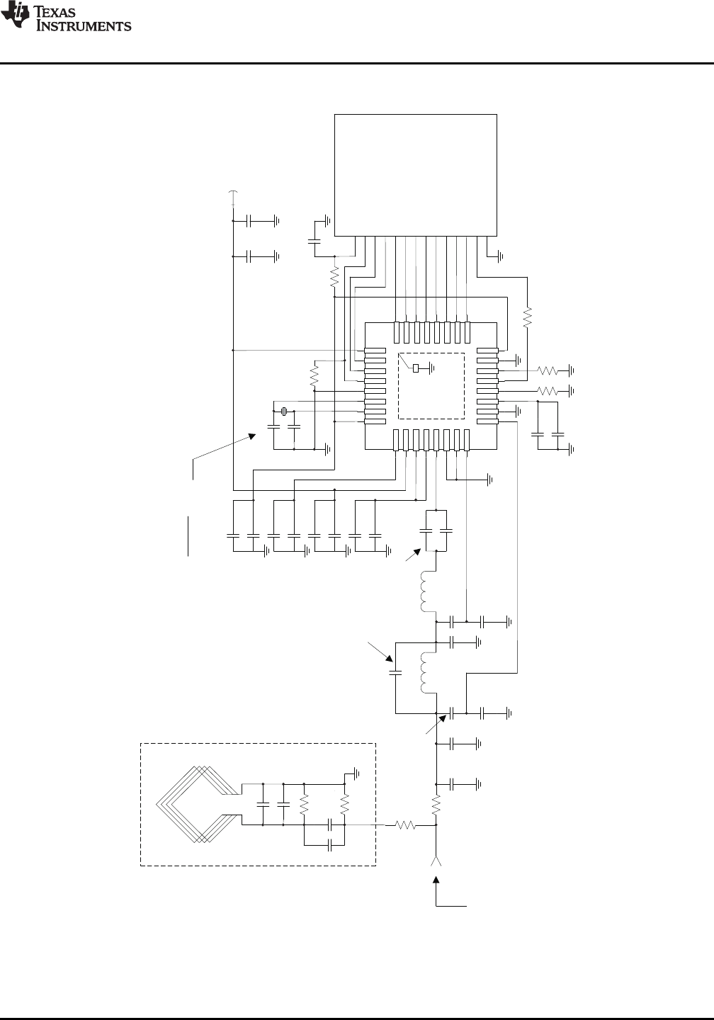
TRF7960
TRF7961
SLOU186F–AUGUST 2006–REVISED AUGUST 2010
www.ti.com
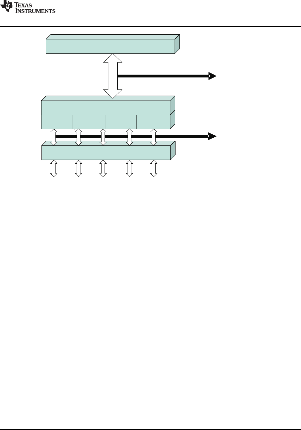
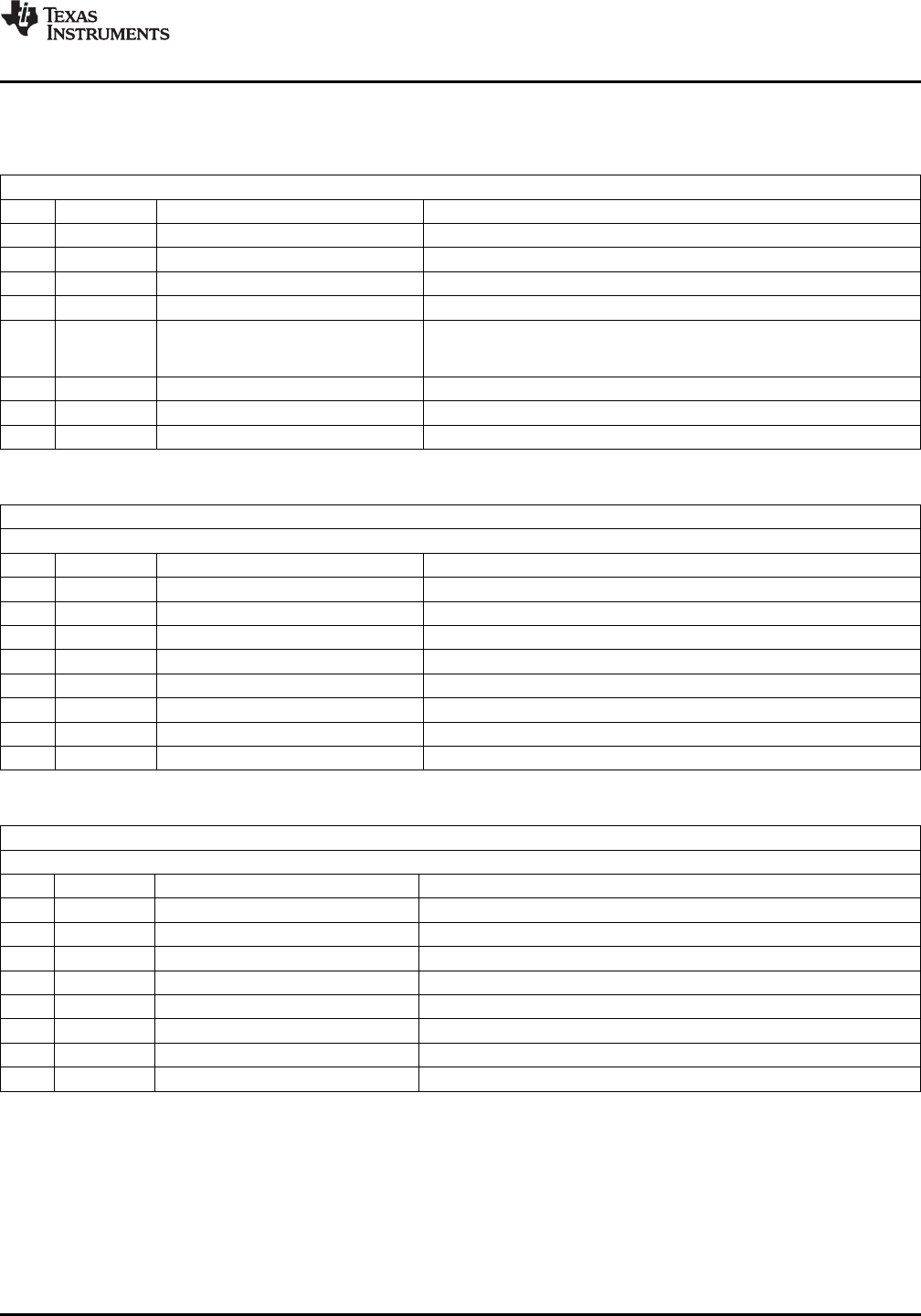
2 Description (continued)
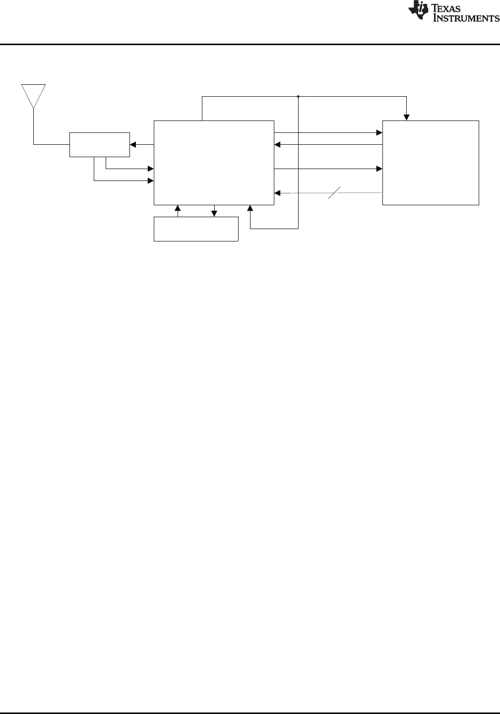
Figure 2-1. Typical Application
A parallel or serial interface can be implemented for communication between the MCU and reader.
Transmit and receive functions use internal encoders and decoders with a 12-byte FIFO register. For
direct transmit or receive functions, the encoders / decoders can be bypassed so the MCU can process
the data in real time. The transmitter has selectable output power levels of 100 mW (20 dBm) or 200 mW
(23 dBm) into a 50-Ωload (5 -V supply) and is capable of ASK or OOK modulation. Integrated voltage
regulators ensure power-supply noise rejection for the complete reader system.
Data transmission comprises low-level encoding for ISO15693, modified Miller for ISO14443-A,
high-bit-rate systems for ISO14443 and Tag-it coding systems. Included with the data encoding is
automatic generation of SOF, EOF, CRC, and / or parity bits.
The receiver system enables AM and PM demodulation using a dual-input architecture. The receiver also
includes an automatic gain control option and selectable gain. Also included is a selectable bandwidth to
cover a broad range of input sub-carrier signal options. The received signal strength for AM and PM
modulation is accessible via the RSSI register. The receiver output is a digitized sub-carrier signal among
a selectable protocol and bit rate as outlined in Table 5-11. A selected decoder delivers bit stream and a
data clock as outputs.
The receiver system also includes a framing system. This system performs CRC and / or parity check,
removes the EOF and SOF settings, and organizes the data in bytes. Framed data is then accessible to
the MCU via a 12-byte FIFO register and MCU interface. The framing supports ISO14443 and ISO15693
protocols.
The TRF7960/61 supports data communication levels from 1.8 V to 5.5 V for the MCU I/O interface, while
also providing a data synchronization clock. An auxiliary 20-mA regulator (pin 32) is available for
additional system circuits.
4Description (continued) Copyright ©2006–2010, Texas Instruments Incorporated
Submit Documentation Feedback
focus.ti.com: TRF7960 TRF7961
TRF7960
TRF7961
www.ti.com
SLOU186F–AUGUST 2006–REVISED AUGUST 2010
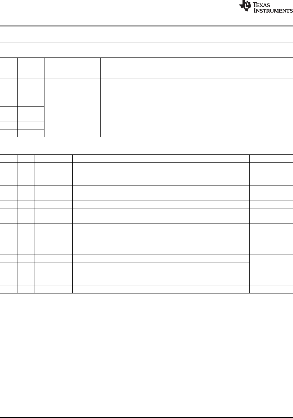
3 Physical Characteristics
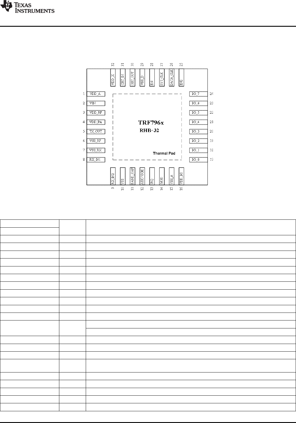
3.1 Terminal Functions
Figure 3-1. TRF796x Pin Assignments (Top View)
Table 3-1. Terminal Functions
TERMINAL TYPE(1) DESCRIPTION
NAME NO.
VDD_A 1 OUT Internal regulated supply (2.7 V –3.4 V) for analog circuitry
VIN 2 SUP External supply input to chip (2.7 V –5.5 V)
VDD_RF 3 OUT Internal regulated supply (2.7 V –5 V), normally connected to VDD_PA (pin 4)
VDD_PA 4 INP Supply for PA; normally connected externally to VDD_RF (pin 3)
TX_OUT 5 OUT RF output (selectable output power, 100 mW at 8 Ωor 200 mW at 4 Ω, with VDD = 5 V)
VSS_RF 6 SUP Negative supply for PA; normally connected to circuit ground
VSS_RX 7 SUP Negative supply for RX inputs; normally connected to circuit ground
RX_IN1 8 INP RX input, used for AM reception
RX_IN2 9 INP RX input, used for PM reception
VSS 10 SUP Chip substrate ground
BAND_GAP 11 OUT Band-gap voltage (1.6 V); internal analog voltage reference; must be ac-bypassed to ground.
Also can be configured to provide the received analog signal output (ANA_OUT)
ASK/OOK 12 BID Direct mode, selection between ASK and OOK modulation (0 = ASK, 1 = OOK)
IRQ 13 OUT Interrupt request
MOD 14 INP Direct mode, external modulation input
VSS_A 15 SUP Negative supply for internal analog circuits; normally connected to circuit ground
Supply for I/O communications (1.8 V –5.5 V). Should be connected to VIN for 5-V
VDD_I/O 16 SUP communication, VDD_X for 3.3-V communication, or any other voltage from 1.8 V to 5.5 V.
I/O_0 17 BID I/O pin for parallel communication
I/O_1 18 BID I/O pin for parallel communication
I/O_2 19 BID I/O pin for parallel communication
I/O_3 20 BID I/O pin for parallel communication
I/O_4 21 BID I/O pin for parallel communication
(1) SUP = Supply, INP = Input, BID = Bi-directional, OUT = Output
Copyright ©2006–2010, Texas Instruments Incorporated Physical Characteristics 5
Submit Documentation Feedback
focus.ti.com: TRF7960 TRF7961
TRF7960
TRF7961
SLOU186F–AUGUST 2006–REVISED AUGUST 2010
www.ti.com
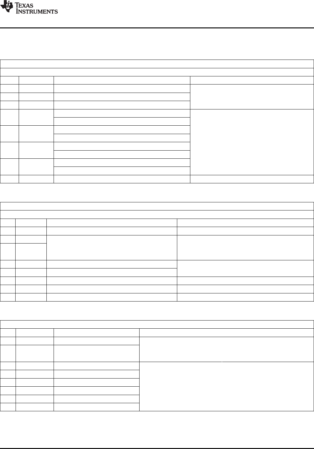
Table 3-1. Terminal Functions (continued)
TERMINAL TYPE(1) DESCRIPTION
NAME NO.
I/O pin for parallel communication
I/O_5 22 BID Strobe out clock for serial communication
Data clock output in direct mode
I/O pin for parallel communication
I/O_6 23 BID MISO for serial communication (SPI)
Serial bit data output in direct mode 1 or sub-carrier signal in direct mode 0
I/O pin for parallel communication.
I/O_7 24 BID MOSI for serial communication (SPI)
Pulse enable and selection of power down mode. If EN2 is connected to VIN, then VDD_X is
EN2 25 INP active during power down to support the MCU. Pin can also be used for pulse wake-up from
power-down mode.
DATA_CLK 26 INP Clock input for MCU communication (parallel and serial)
Clock for MCU (3.39 / 6.78 / 13.56 MHz) at EN = 1 and EN2 = don't care
SYS_CLK 27 OUT If EN = 0 and EN2 = 1, then system clock is set to 60 kHz
EN 28 INP Chip enable input (If EN = 0, then chip is in power-down mode).
VSS_D 29 SUP Negative supply for internal digital circuits; normally connected to circuit ground
OSC_OUT 30 OUT Crystal oscillator output
OSC_IN 31 INP Crystal oscillator input
VDD_X 32 OUT Internally regulated supply (2.7 V –3.4 V) for external circuitry (MCU)
Thermal Pad Connected to circuit ground
3.2 PACKAGING/ORDERING INFORMATION(1)
PACKAGED DEVICES PACKAGE TYPE (2) TRANSPORT MEDIA QUANTITY
TRF7960RHBT Tape and reel 250
RHB-32
TRF7960RHBR Tape and reel 3000
TRF7961RHBT Tape and reel 250
RHB-32
TRF7961RHBR Tape and reel 3000
(1) For the most current package and ordering information, see the Package Option Addendum at the end of this document, or see the TI
Web site at www.ti.com.
(2) Package drawings, standard packing quantities, thermal data, symbolization, and PCB design guidelines are available at
www.ti.com/sc/package .
6Physical Characteristics Copyright ©2006–2010, Texas Instruments Incorporated
Submit Documentation Feedback
focus.ti.com: TRF7960 TRF7961
TRF7960
TRF7961
www.ti.com
SLOU186F–AUGUST 2006–REVISED AUGUST 2010
4 ELECTRICAL SPECIFICATIONS
4.1 ABSOLUTE MAXIMUM RATINGS
over operating free-air temperature range (unless otherwise noted)(1)
VALUE UNIT
VIN Supply voltage 6 V
IOOutput current 150 mA
Continuous power dissipation See Dissipation Ratings Table
Maximum junction temperature, any condition(2) 140 °C
TJMaximum junction temperature, continuous operation, long-term reliability(2) 125 °C
Tstg Storage temperature range –55 to 150 °C
Lead temperature 1,6 mm (1/16 inch) from case for 10 seconds 300 °C
HBM (human body model) 2 kV
ESDS rating CDM (charged device model) 500 V
MM (machine model) 200
(1) The absolute maximum ratings under any condition is limited by the constraints of the silicon process. Stresses above these ratings may
cause permanent damage. Exposure to absolute maximum conditions for extended periods may degrade device reliability. These are
stress ratings only and functional operation of the device at these or any other conditions beyond those specified are not implied.
(2) The maximum junction temperature for continuous operation is limited by package constraints. Operation above this temperature may
result in reduced reliability and/or lifetime of the device.
4.2 DISSIPATION RATINGS TABLE
POWER RATING(2)
θJC θJA (1)
PACKAGE (°C/W) (°C/W) TA≤25°C TA= 85°C
RHB (32) 31 36.4 2.7 W 1.1 W
(1) This data was taken using the JEDEC standard high-K test PCB.
(2) Power rating is determined with a junction temperature of 125°C. This is the point where distortion starts to increase substantially.
Thermal management of the final PCB should strive to keep the junction temperature at or below 125°C for best performance and
long-term reliability.
4.3 RECOMMENDED OPERATING CONDITIONS
over operating free-air temperature range (unless otherwise noted)
MIN TYP MAX UNIT
VIN Supply voltage 2.7 5 5.5 V
TJOperating virtual junction temperature range –40 125 °C
TAOperating ambient temperature range –40 25 110 °C
Copyright ©2006–2010, Texas Instruments Incorporated ELECTRICAL SPECIFICATIONS 7
Submit Documentation Feedback
focus.ti.com: TRF7960 TRF7961

TRF7960
TRF7961
SLOU186F–AUGUST 2006–REVISED AUGUST 2010
www.ti.com
4.4 ELECTRICAL CHARACTERISTICS
over temperature range VS= 5 V (unless otherwise noted)
TYP
–40°C
PARAMETER CONDITIONS MIN/
25°C TO UNIT MAX
110°C
IPD Supply current in power-down mode All systems disabled, including supply-voltage regulators 1 10 μA MAX
The reference voltage generator and the VDD_X remain
IPD2 Supply current in power-down mode 2 120 300 μA MAX
active to support external circuitry.
Oscillator running, supply-voltage regulators in
ISTBY Supply current in standby mode 1.5 4 mA MAX
low-consumption mode
Supply current without antenna driver Oscillator, regulators, Rx and AGC, are all active. Tx is
ION1 10 16 mA MAX
current off.
Supply current with antenna driver Oscillator, regulators, Rx, AGC, and Tx are all active.
ION2 70 mA MAX
current Pout = 100 mW.
Supply current with antenna driver Oscillator, regulators, Rx, AGC, and Tx are all active.
ION3 120 mA MAX
current Pout = 200 mW.
1.4 MIN
BG Band Gap voltage Internal analog reference voltage 1.6 V
1.7 MAX
1.4 MIN
VPOR Power on reset voltage (POR) 2 V
2.5 MAX
3.1 MIN
VDD_A Regulated supply for analog circuitry 3.5 V
3.8 MAX
4 MIN
VDD_RF Regulated supply for RF circuitry Regulator set for 5-V system with 250-mV difference. 4.6 V
5.2 MAX
3.1 MIN
VDD_X Regulated supply for external circuitry 3.4 V
3.8 MAX
The difference between the external supply and the
Rejection of external supply noise on
PPSRR regulated voltage is higher than 250 mV. Measured at 26 20 dB MIN
the supply VDD_RF regulator 212 kHz.
Half-power mode 8 12 ΩMAX
RRFOUT PA driver output resistance Full- power mode 4 6 ΩMAX
5 MIN
RRFIN RX_IN1 and RX_IN2 input resistance 10 kΩ
20 MAX
VRFIN Maximum input voltage At RX_IN1 and RX_IN2 inputs 3.5 VPP MAX
fSUB-CARRIER = 424 kHz 1.2 2.5 mVPP MAX
VSENS Input sensitivity fSUB-CARRIER = 848 kHz 1.2 3 mVPP MAX
tSET_PD Set up time after power down 10 20 ms MAX
tSET_STBY Set up time after standby mode 30 100 μs MAX
Recovery time after modulation
tREC Modulation signal: sine, 424-kHz, 10-mVpp 60 μs MAX
(ISO14443)
30 MIN
fSYS_CLK SYS_CLK frequency In PD2 mode EN = 0 and EN2 = 1 60 kHz
120 MAX
CLKMAX Maximum CLK frequency 2 MHz TYP
VIL Input logic low 0.2 0.2 VDD_I/O MAX
VIH Input logic high 0.8 VDD_I/O MIN
ROUT Output resistance I/O_0 to I/O_7 low_io = H for VDD_I/O <2.7 V 400 800 ΩMAX
RSYS_CLK Output resistance SYS_CLK low_io = H for VDD_I/O <2.7 V 200 400 ΩMAX
8ELECTRICAL SPECIFICATIONS Copyright ©2006–2010, Texas Instruments Incorporated
Submit Documentation Feedback
focus.ti.com: TRF7960 TRF7961
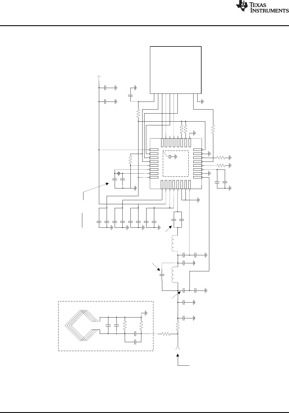
Test Port
or
Ext AntPort
1
TRF796x
RHB-32
2
3
4
5
6
7
8
9 10 11 12 13 14 15 16
32 31 30 29 28 27 26 25
17
18
19
20
21
22
23
24
33
ThermalPad
VDD_X
OSC_IN
OSC_OUT
VSS_D
EN
SYS_CLK
DATA_CLK
EN2
VDD_I /O
VSS_A
MOD
IRQ
ASK/OOK
BANDGAP
VSS
RX2_PM
RX1_AM
VDD_A
VSS_RX
VSS_RF
TX_OUT
VDD_PA
VDD_RF
VIN
I/O_0
I/O_1
I/O_2
I/O_3
I/O_4
I/O_5
I/O_6
I/O_7
1000pF
1000pF
1500pF
1500pF
680pF
680pF
220pF
VSWR
Adj
Phase Adj
330nH 150nH
Freq Adj
100pF
27pF
2.2uF
10nF
10nF
10nF
10nF
2.2uF
2.2uF
2.2uF
0Ohms
0Ohms
27pF
27pF
13.56MHz
VSWR Adj
DVcc
D/AVss
XIN
1K
1K
ReaderPwrEnable(GPIO)
InterruptCapableGPIO
MSP430 (Family)
4.7uF
10V
0.1uF
1K
CLK(GPIO)
PX.7
PX.6
PX.5
PX.4
PX.3
PX.2
PX.1
PX.0
Vcc
100
0.1uF
2.2uF
10nF
10K
10pF
Harmonic
Suppression
C1 C2´
Xtal CLCS
C1+C2
=+
Antenna
Circuit
Ant “Q”
Adj
R “cal”
open/short/load
TRF7960
TRF7961
www.ti.com
SLOU186F–AUGUST 2006–REVISED AUGUST 2010
4.5 Application Schematic for the TRF796x EVM (Parallel Mode)
Copyright ©2006–2010, Texas Instruments Incorporated ELECTRICAL SPECIFICATIONS 9
Submit Documentation Feedback
focus.ti.com: TRF7960 TRF7961
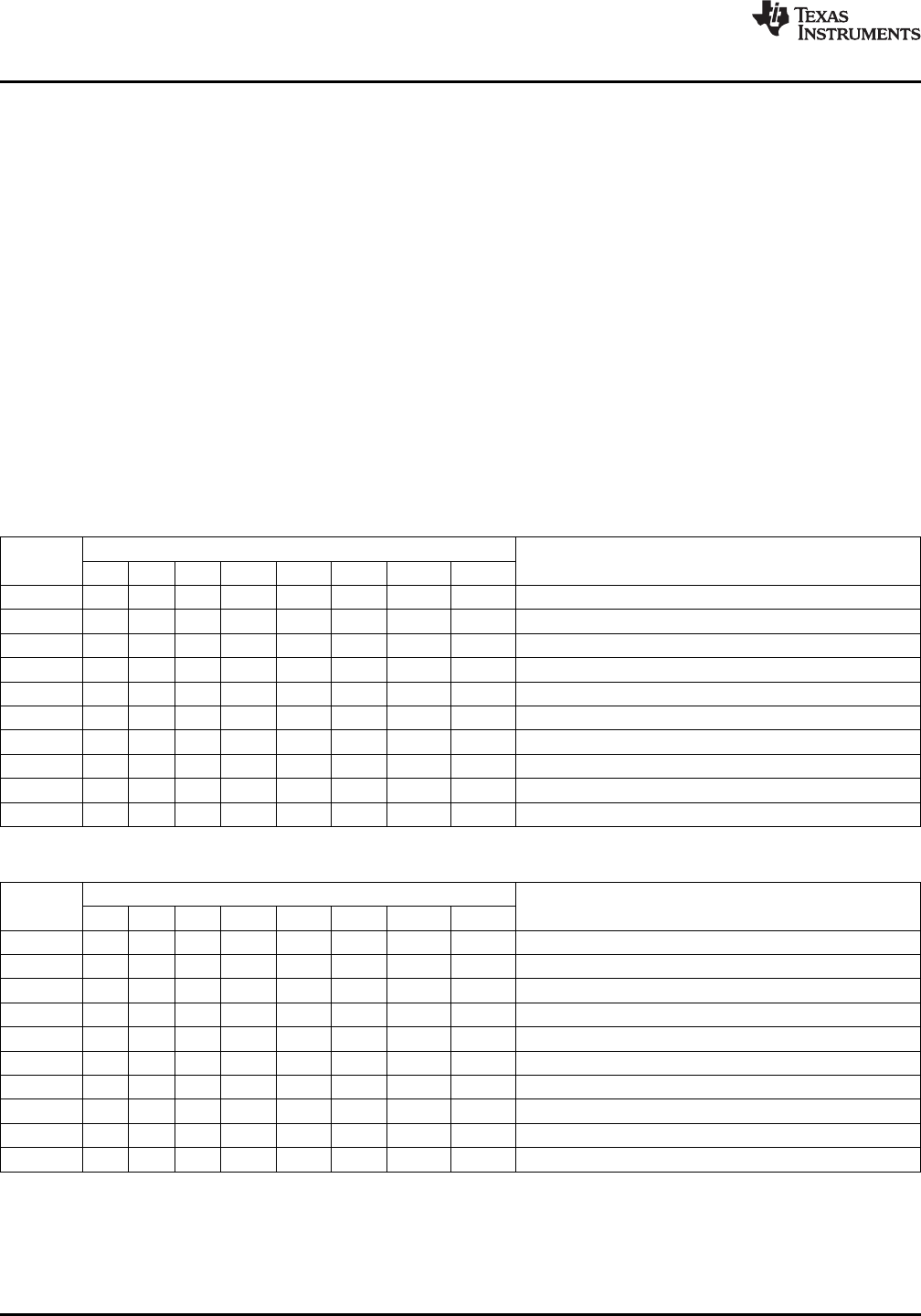
TestPort
or
Ext AntPort
1
TRF796x
RHB-32
2
3
4
5
6
7
8
9 10 11 12 13 14 15 16
32 31 30 29 28 27 26 25
17
18
19
20
21
22
23
24
33
ThermalPad
VDD_X
OSC_IN
OSC_OUT
VSS_D
EN
SYS_CL
DATA_CLK
EN2
VDD_I /O
VSS_A
MOD
IRQ
ASK/
BANDGAP
VSS
RX2_PM
RX1_AM
VDD_A
VSS_RX
VSS_RF
TX_OUT
VDD_PA
VDD_RF
VIN
I/O_0
I/O_1
I/O_2
I/O_3
I/O_4
I/O_5
I/O_6
I/O_7
1000pF
1000pF
1500pF
1500pF
680pF
680pF
220pF
VSWR
Adj
Phase Adj 330nH 150nH
Freq Adj
100pF
27pF
2.2 Fµ
10nF
10nF
10nF
10nF
2.2 Fµ
2.2 Fµ
2.2 Fµ
0Ohms
0Ohms
27pF
27pF
13.56MHz
VSWR Adj
Vcc
DVcc
D/AVss
MISO
MOSI
XIN
10K
10K
1K
1K
CLK(GPIO)
SlaveSelect(GPIO)
ReaderPwrEnable(GPIO)
InterruptCapableGPIO
MSP430(Family)
4.7 F
10V
µ
0.1 Fµ
1K
100
0.1 Fµ
2.2 Fµ
10nF
10pF
Harmonic
Suppression
10K
C1 C2´
Xtal CLCS
C1+C2
=+
Antenna
Circuit
Ant “Q”
Adj
R “cal”
open/short/load
TRF7960
TRF7961
SLOU186F–AUGUST 2006–REVISED AUGUST 2010
www.ti.com
4.6 Application Schematic for the TRF796x EVM (SPI Mode)
10 ELECTRICAL SPECIFICATIONS Copyright ©2006–2010, Texas Instruments Incorporated
Submit Documentation Feedback
focus.ti.com: TRF7960 TRF7961

TRF7960
TRF7961
www.ti.com
SLOU186F–AUGUST 2006–REVISED AUGUST 2010
5 System Description
5.1 Power Supplies
The positive supply pin, VIN (pin 2) has an input voltage range of 2.7 V to 5.5 V. The positive supply input
sources three internal regulators with output voltages VDD_RF, VDD_A and VDD_X that use external bypass
capacitors for supply noise filtering. These regulators provide enhanced PSRR for the RFID reader
system.
The regulators are not independent and have common control bits for output voltage setting. The
regulators can be configured to operate in either automatic or manual mode. The automatic regulator
mode setting ensures an optimal compromise between regulator PSRR and highest possible supply
voltage for RF output power. Whereas, the manual mode allows the user to manually configure the
regulator settings.
VDD_RF The regulator VDD_RF (pin 3) is used to source the RF output stage. The voltage regulator can
be set for either 5-V or 3-V operation. When configured for the 5-V operation, the output
voltage can be set from 4.3 V to 5 V in 100-mV steps. The current sourcing capability for 5-V
operation is 150 mA maximum over the adjusted output voltage range.
When configured for 3-V operation, the output can be set from 2.7 V to 3.4 V, also in 100-mV
steps. The current sourcing capability for 3-V operation is 100 mA maximum over the adjusted
output voltage range.
VDD_A Regulator VDD_A (pin 1) supplies voltage to analog circuits within the reader chip. The voltage
setting is divided in two ranges. When configured for 5-V operation, the output voltage is fixed
at 3.5 V.
When configured for 3-V operation, the output can be set from 2.7 V to 3.4 V in 100-mV steps.
Note that when configured, both VDD_A and VDD_X regulators are configured together
(their settings are not independent).
VDD_X Regulator VDD_X (pin 32) can be used to source the digital I/O of the reader chip together with
other external system components. When configured for 5-V operation, the output voltage is
fixed at 3.4 V.
When configured for 3-V operation, the output voltage can be set from 2.7 to 3.4 V in 100-mV
steps. The total current sourcing capability of the VDD_X regulator is 20 mA maximum over the
adjusted output range. Note that when configured, both VDD_A and VDD_X regulators are
configured together (their settings are not independent).
VDD_PA The VDD_PA pin (pin 4) is the positive supply pin for the RF output stage and is externally
connected to the regulator output VDD_RF (pin 3).
5.1.1 Negative Supply Connections
The negative supply connections are all externally connected together (to GND). The substrate connection
is VSS (pin 10), the analog negative supply is VSS_A (pin 15), the logic negative supply is VSS_D (pin 29),
the RF output stage negative supply is VSS_TX (pin 6), and the negative supply for the RF receiver input is
VSS_RX (pin 7).
5.1.2 Digital I/O Interface
To allow compatible I/O signal levels, the TRF7960/61 has a separate supply input VDD_I/O (pin 16), with
an input voltage range of 1.8 V to 5.5 V. This pin is used to supply the I/O interface pins (I/O_0 to I/O_7),
IRQ, SYS_CLK, and DATA_CLK pins of the reader. In typical applications, VDD_I/O is connected directly to
VDD_X to ensure that the I/O signal levels of the MCU are the same as the internal logic levels of the
reader.
Copyright ©2006–2010, Texas Instruments Incorporated System Description 11
Submit Documentation Feedback
focus.ti.com: TRF7960 TRF7961
TRF7960
TRF7961
SLOU186F–AUGUST 2006–REVISED AUGUST 2010
www.ti.com
5.1.3 Supply Regulator Configuration
The supply regulators can be automatically or manually configured by the control bits. The available
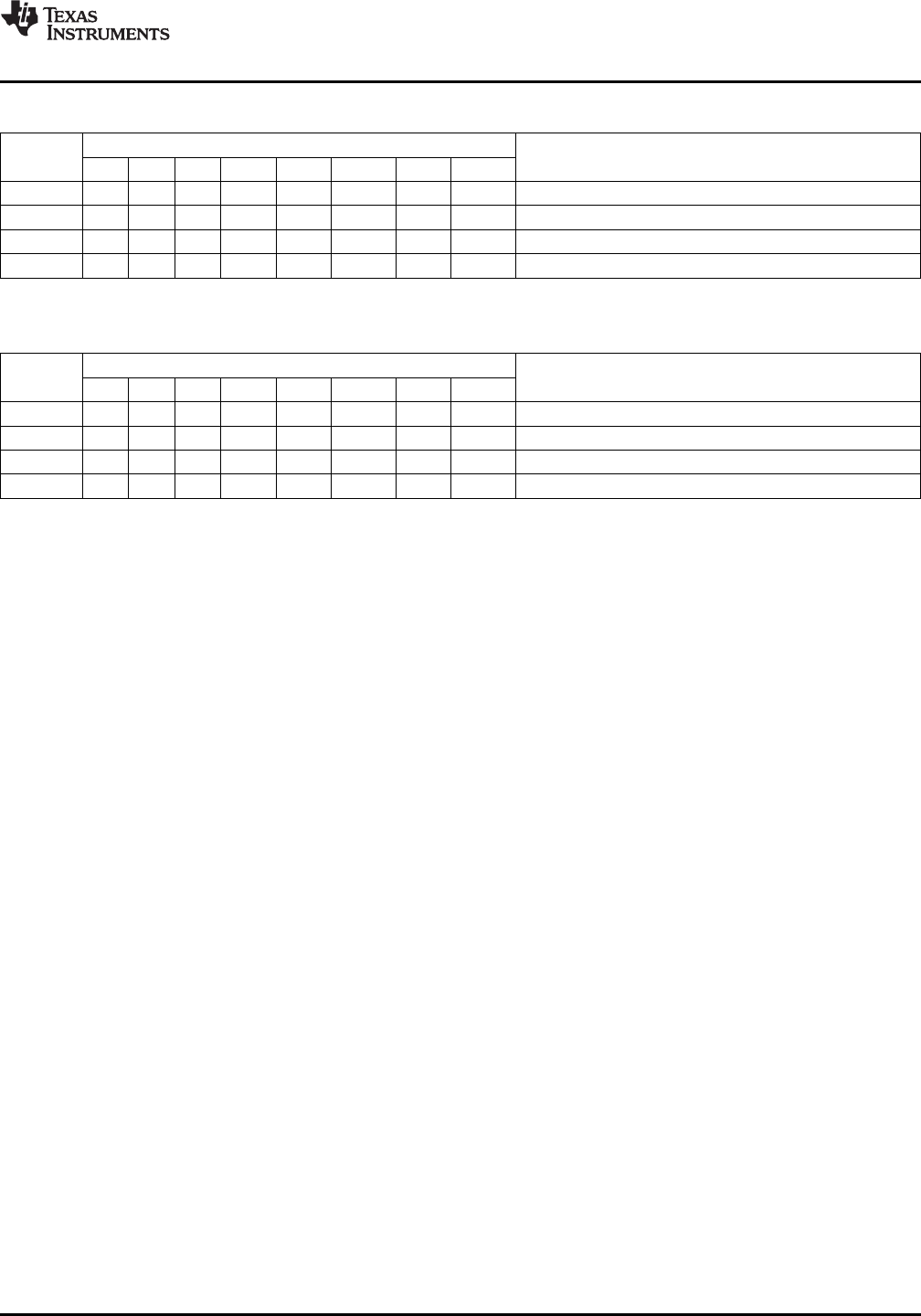
options are shown in Table 5-1 through Table 5-4.Table 5-1 shows a 5-V system and the manual-mode
regulator settings. Table 5-2 shows manual mode for selection of a 3-V system. Table 5-3 and Table 5-4
show the automatic-mode gain settings for 5-V and 3-V systems.
The automatic mode is the default configuration. In automatic mode, the regulators are automatically set
every time the system is activated by asserting the EN input HIGH. The internal regulators are also
automatically reconfigured every time the automatic regulator selection bit is set HIGH (on the rising
edge).
The user can re-run the automatic mode setting from a state in which the automatic setting bit is already
high by changing the automatic setting bit from high to low to high. The regulator-configuration algorithm
adjusts the regulator outputs 250 mV below the VIN level, but not higher than 5 V for VDD_RF, 3.5 V for
VDD_A, and 3.4 V for VDD_X. This ensures the highest possible supply voltage for the RF output stage while
maintaining an adequate PSRR (power supply rejection ratio). As an example, the user can improve the
PSRR if there is a noisy supply voltage from VDD_X by increasing the target voltage difference across the
VDD_X regulator as shown for automatic regulator settings in Table 5-3 and Table 5-4.
Table 5-1. Supply-Regulator Setting –Manual –5-V System
Byte Option Bits Setting in Control Register Action
Address B7 B6 B5 B4 B3 B2 B1 B0
00 1 5-V system
0B 0 Manual regulator setting
0B 0 1 1 1 VDD_RF = 5 V, VDD_A = 3.5 V, and VDD_X = 3.4 V
0B 0 1 1 0 VDD_RF = 4.9 V, VDD_A = 3.5 V, and VDD_X = 3.4 V
0B 0 1 0 1 VDD_RF = 4.8 V, VDD_A = 3.5 V, and VDD_X = 3.4 V
0B 0 1 0 0 VDD_RF = 4.7 V, VDD_A = 3.5 V, and VDD_X = 3.4 V
0B 0 0 1 1 VDD_RF = 4.6 V, VDD_A = 3.5 V, and VDD_X = 3.4 V
0B 0 0 1 0 VDD_RF = 4.5 V, VDD_A = 3.5 V, and VDD_X = 3.4 V
0B 0 0 0 1 VDD_RF = 4.4 V, VDD_A = 3.5 V, and VDD_X = 3.4 V
0B 0 0 0 0 VDD_RF = 4.3 V, VDD_A = 3.5 V, and VDD_X = 3.4 V
Table 5-2. Supply-Regulator Setting –Manual –3-V System
Byte Option Bits Setting in Control Register Action
Address B7 B6 B5 B4 B3 B2 B1 B0
00 0 3V system
0B 0 Manual regulator setting
0B 0 1 1 1 VDD_RF = 3.4 V, VDD_A, and VDD_X = 3.4 V
0B 0 1 1 0 VDD_RF = 3.3 V, VDD_A, and VDD_X = 3.3 V
0B 0 1 0 1 VDD_RF = 3.2 V, VDD_A, and VDD_X = 3.2 V
0B 0 1 0 0 VDD_RF = 3.1 V, VDD_A, and VDD_X = 3.1 V
0B 0 0 1 1 VDD_RF = 3.0 V, VDD_A, and VDD_X = 3.0 V
0B 0 0 1 0 VDD_RF = 2.9 V, VDD_A, and VDD_X = 2.9 V
0B 0 0 0 1 VDD_RF = 2.8 V, VDD_A, and VDD_X = 2.8 V
0B 0 0 0 0 VDD_RF = 2.7 V, VDD_A, and VDD_X = 2.7 V
12 System Description Copyright ©2006–2010, Texas Instruments Incorporated
Submit Documentation Feedback
focus.ti.com: TRF7960 TRF7961
TRF7960
TRF7961
www.ti.com
SLOU186F–AUGUST 2006–REVISED AUGUST 2010
Table 5-3. Supply-Regulator Setting –Automatic –5-V System
Byte Option Bits Setting in Control Register Action
Address B7 B6 B5 B4 B3 B2(1) B1 B0
00 1 5-V system
0B 1 x 1 1 Automatic regulator setting ≉250-mV difference
0B 1 x 1 0 Automatic regulator setting ≉350-mV difference
0B 1 x 0 0 Automatic regulator setting ≉400-mV difference
(1) X are don't cares
Table 5-4. Supply-Regulator Setting –Automatic –3-V System
Byte Option Bits Setting in Control Register Action
Address B7 B6 B5 B4 B3 B2(1) B1 B0
00 0 3-V system
0B 1 x 1 1 Automatic regulator setting ≉250-mV difference
0B 1 x 1 0 Automatic regulator setting ≉350-mV difference
0B 1 x 0 0 Automatic regulator setting ≉400-mV difference
(1) X are don't cares
5.1.4 Power Modes
The chip has seven power states, which are controlled by two input pins (EN and EN2) and three bits in
the chip status control register (00h).
The main reader enable input is EN (which has a threshold level of 1 V minimum). Any input signal level
from 1.8 V to VIN can be used. When EN is set high, all of the reader regulators are enabled, together with
the 13.56-MHz oscillator, while the SYS_CLK (output clock for external micro controller) is made available.
The auxiliary-enable input EN2 has two functions. A direct connection from EN2 to VIN ensures availability
of the regulated supply (VDD_X) and an auxiliary clock signal (60 kHz) on the SYS_CLK output (same for
the case EN = 0). This mode is intended for systems in which the MCU controlling the reader is also being
supplied by the reader supply regulator (VDD_X) and the MCU clock is supplied by the SYS_CLK output of
the reader. This allows the MCU supply and clock to be available during power-down.
A second function of the EN2 input is to enable start-up of the reader system from complete power down
(EN = 0, EN2 = 0). In this case the EN input is being controlled by the MCU or other system device that is
without supply voltage during complete power down (thus unable to control the EN input). A rising edge
applied to the EN2 input (which has a 1-V threshold level) starts the reader supply system and 13.56-MHz
oscillator (identical to condition EN = 1). This start-up mode lasts until all of the regulators have settled
and the 13.56-MHz oscillator has stabilized. If the EN input is set high by the MCU (or other system
device), the reader stays active. If the EN input is not set high within 100 μs after the SYS_CLK output is
switched from auxiliary clock (60 kHz) to high-frequency clock (derived from the crystal oscillator), the
reader system returns to complete power-down mode. This option can be used to wake the reader system
from complete power down by using a push-button switch or by sending a single pulse.
Copyright ©2006–2010, Texas Instruments Incorporated System Description 13
Submit Documentation Feedback
focus.ti.com: TRF7960 TRF7961
TRF7960
TRF7961
SLOU186F–AUGUST 2006–REVISED AUGUST 2010
www.ti.com
After the reader EN line is high, the other power modes are selected by control bits. The power mode
options and functions are listed in Table 5-5.
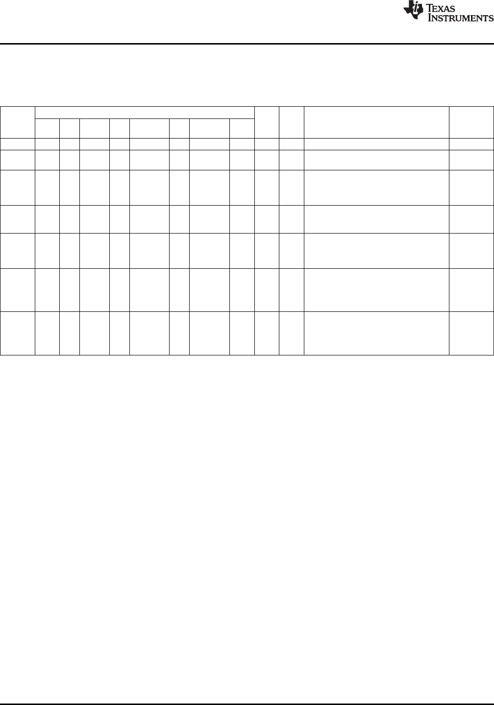
Table 5-5. Power Modes
Byte Option Bits Setting in Chip Status Control Register EN EN2 Functionality Current
Address B7 B6 B5 B4 B3 B2 B1 B0
STBY RFON RF PWR REC ON
00 0 0 Complete power down <1μA
00 0 1 VDD_X available 120 μA
SYS_CLK auxiliary frequency 60 kHz is ON
00 1 x x x 1 x All supply regulators active and in low power 1.5 mA
mode
13.56-MHz oscillator ON
SYS_CLK clock available
00 0 0 x 0 1 x All supply regulators active 3.5 mA
13.56-MHz oscillator ON
SYS_CLK clock available
00 0 0 x 1 1 x All supply regulators active 10 mA
13.56-MHz oscillator ON
SYS_CLK clock available
Receiver active
00 0 1 1 x 1 x All supply regulators active 70 mA
13.56-MHz oscillator ON (at 5 V)
SYS_CLK clock available
Receiver active
Transmitter active –half-power mode
00 0 1 0 x 1 x All supply regulators active 120 mA
13.56-MHz oscillator running (at 5 V)
SYS_CLK clock available
Receiver active
Transmitter active –full-power mode
During reader inactivity, the TRF7960/61 can be placed in power down-mode (EN = 0). The power down
can be complete (EN = 0, EN2 = 0) with no function running, or partial (EN = 0, EN2 = 1) where the
regulated supply (VDD_X) and auxiliary clock 60 kHz (SYS_CLK) are available to the MCU or other system
device.
When EN is set high (or on rising edge of EN2 and then confirmed by EN = 1), the supply regulators are
activated and the 13.56-MHz oscillator started. When the supplies are settled and the oscillator frequency
is stable, the SYS_CLK output is switched from the auxiliary frequency of 60 kHz to the selected
frequency derived from the crystal oscillator. At this point, the reader is ready to communicate and perform
the required tasks. The control system (MCU) can then write appropriate bits to the chip status control
register (address 00) and select the operation mode.
The STANDBY mode (bit 7 = 1 of register 00) is the active mode with the lowest current consumption. The
reader is capable of recovering from this mode to full operation in 100 μs.
The active mode with RF section disabled (bit 5 = 0 and bit 1 = 0 of register 00) is the next active mode
with low power consumption. The reader is capable of recovering from this mode to full operation in 25 μs.
The active mode with only the RF receiver section active (bit 1 = 1 of register 00) can be used to measure
the external RF field (as described in RSSI measurements paragraph) if reader-to-reader anticollision is
implemented.
The active mode with the entire RF section active (bit 5 = 1 of register 00) is the normal mode used for
transmit and receive operations.
14 System Description Copyright ©2006–2010, Texas Instruments Incorporated
Submit Documentation Feedback
focus.ti.com: TRF7960 TRF7961
C001
C002
TRF7960
TRF7961
www.ti.com
SLOU186F–AUGUST 2006–REVISED AUGUST 2010
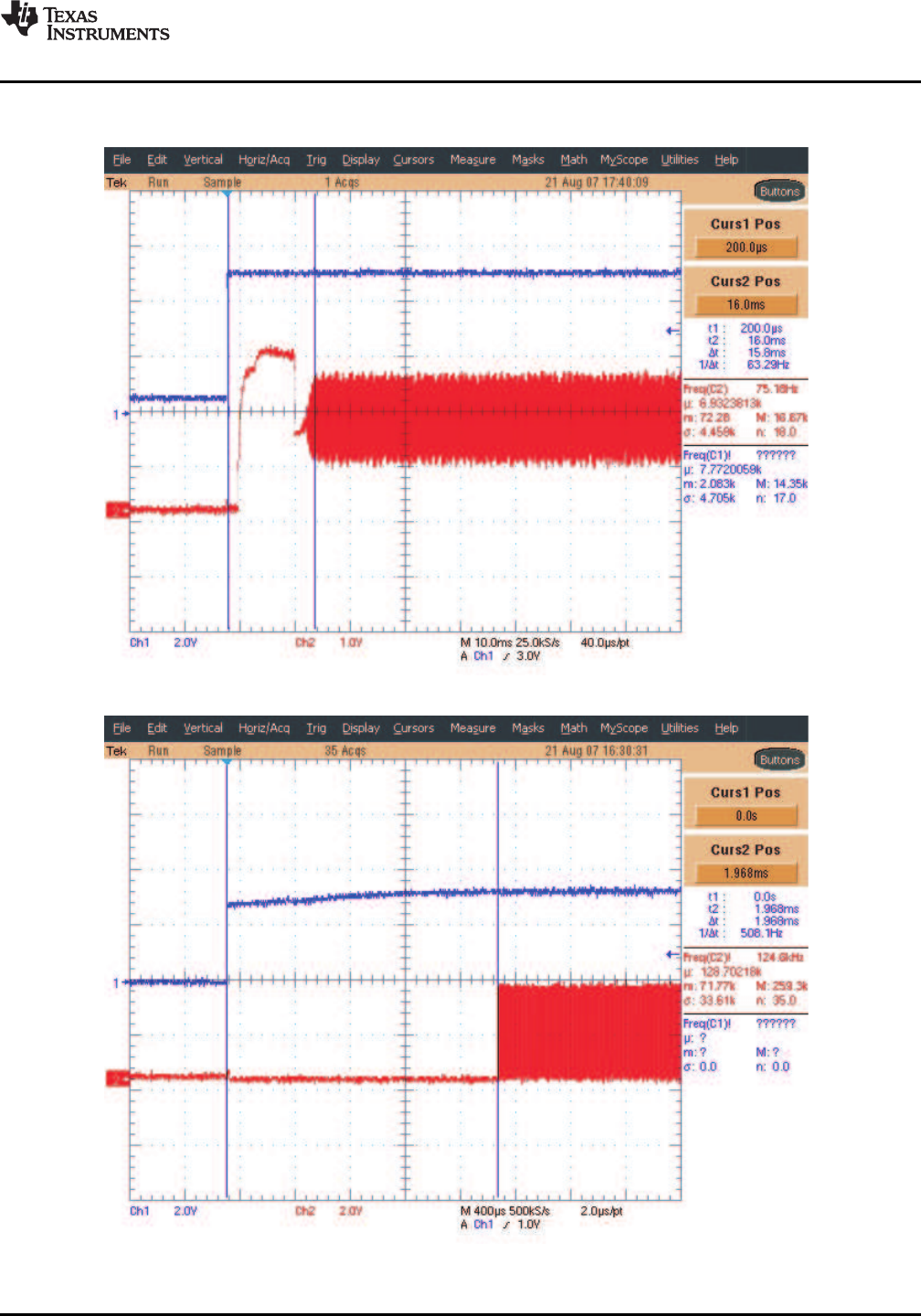
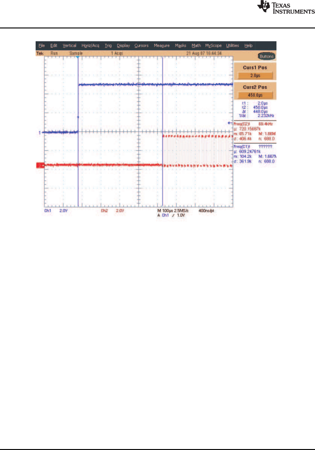
5.1.5 Timing Diagrams
CHIP POWER UP TO CLOCK START
Figure 5-1. Power Up [VIN (Blue) to Crystal Start (Red)]
CHIP ENABLE TO CLOCK START
Figure 5-2. EN2 Low and EN High (Blue) to Start of System Clock (Red)
Copyright ©2006–2010, Texas Instruments Incorporated System Description 15
Submit Documentation Feedback
focus.ti.com: TRF7960 TRF7961

TRF7960
TRF7961
www.ti.com
SLOU186F–AUGUST 2006–REVISED AUGUST 2010
5.2 Receiver –Analog Section
The TRF7960/61 has two receiver inputs, RX_IN1 (pin 8) and RX_IN2 (pin 9). The two inputs are
connected to an external filter to ensure that AM modulation from the tag is available on at least one of the
two inputs. The external filter provides a 45°phase shift for the RX_IN2 input to allow further processing of
a received PM-modulated signal (if it appears) from the tag. This architecture eliminates any possible
communication holes that may occur from the tag to the reader.
The two RX inputs are multiplexed to two receiver channels: the main receiver and the auxiliary receiver.
Receiver input multiplexing is controlled by control bit B3 (pm-on) in the chip status control register
(address 00). The main receiver is composed of an RF-detection stage, gain, filtering with AGC, and a
digitizing stage whose output is connected to the digital processing block. The main receiver also has an
RSSI measuring stage, which measures the strength of the demodulated signal.
The primary function of the auxiliary receiver is to measure the RSSI of the modulation signal. It also has
similar RF-detection, gain, filtering with AGC, and RSSI blocks.
The default setting is RX_IN1 connected to the main receiver and RX_IN2 connected to the auxiliary
receiver (bit pm_on = 0). When a response from the tag is detected by the RSSI, values on both inputs
are measured and stored in the RSSI level register (address 0F). The control system reads the RSSI
values and switches to the stronger receiver input (RX_IN1 or RX_IN2 by setting pm_on = 1).
The receiver input stage is an RF level detector. The RF amplitude level on RX_IN1 and RX_IN2 inputs
should be approximately 3 VPP for a VIN supply level greater than 3.3 V. If the VIN level is lower, the RF
input peak-to-peak voltage level should not exceed the VIN level. Note: VIN is the main supply voltage to
the device at pin 2.
The first gain and filtering stage following the RF-envelope detector has a nominal gain of 15 dB with an
adjustable bandpass filter. The bandpass filter has adjustable 3-dB frequency steps (100 kHz to 400 kHz
for high pass and 600 kHz to 1500 kHz for low pass). Following the bandpass filter is another
gain-and-filtering stage with a nominal gain of 8 dB and with frequency characteristics identical to the first
stage.
The internal filters are configured automatically, with internal presets for each new selection of a
communication standard in the ISO control register (address 01). If required, additional fine tuning can be
accomplished by writing directly to the RX special setting registers (address 0A).
The second receiver gain stage and digitizer stage are included in the AGC loop. The AGC loop is
activated by setting the bit B2 = 1 (agc-on) in the chip status control register (address 00). When
activated, the AGC continuously monitors the input signal level. If the signal level is significantly higher
than an internal threshold level, gain reduction is activated. AGC activation is by default five times the
internal threshold level. It can be reduced to three times the internal level by setting bit B1 = 1 (agcr) in the
RX special setting register (address 0A). The AGC action is fast, typically finishing after four sub-carrier
pulses. By default, the AGC action is blocked after the first few pulses of the sub-carrier signal. This
prevents the AGC from interfering with the reception of the remaining data packet. In certain situations,
this type of blocking is not optimal, so it can be removed by setting B0 = 1 (no_lim) in the RX special
setting register (address 0A).
The bits of the RX special settings register (address 0A), which control the receiver analog section, are
shown in Table 5-20.
5.2.1 Received Signal Strength Indicator (RSSI)
The RSSI measurement block measures the demodulated signal (except in the case of a direct command
for RF-amplitude measurement described in the Direct Commands section). The measuring system
latches the peak value, so the RSSI level can be read after the end of the receive packet. The RSSI
register values reset with every transmission by the reader. This allows an updated RSSI measurement
for each new tag response.
Copyright ©2006–2010, Texas Instruments Incorporated System Description 17
Submit Documentation Feedback
focus.ti.com: TRF7960 TRF7961
TRF7960
TRF7961
SLOU186F–AUGUST 2006–REVISED AUGUST 2010
www.ti.com
Correlation between the RF input level and RSSI designation levels on the RX_IN1 and RX_IN2 are
shown in Table 5-6 and Table 5-7.
Table 5-6 shows the RSSI level versus RSSI bit value. The RSSI has seven levels (3 bits each) with 4-dB
increments. The input level is the peak-to-peak modulation level of the RF signal as measured on one side
envelope (positive or negative).
Table 5-6. RSSI Level Versus Register Bit Value
RSSI1234567
Input level 2 mVpp 3.2 mVpp 5 mVpp 8 mVpp 13 mVpp 20 mVpp 32 mVpp
As an example, from Table 5-7, let B2 = 1, B1 = 1, B0 = 0; this yields an RSSI value of 6. From Table 5-6
a Bit value of 6 would yield an RSSI level of 20 mVpp.
Table 5-7. RSSI Bit Value and Oscillator Status Register (0F)
Bit Signal Name Function Comments
B7 Unused
B6 osc_ok Crystal oscillator stable
B5 rssi_x2 MSB of auxiliary receiver RSSI
B4 rssi_x1 Auxiliary receiver RSSI
B3 rssi_x1 LSB of auxiliary receiver RSSI 4 dB per step
B2 rssi_2 MSB of main receiver RSSI
B1 rssi_1 Main receiver RSSI
B0 rssi_0 LSB of main receiver RSSI
5.2.2 Receiver –Digital Section
The received sub-carrier is digitized to form a digital representation of the modulated RF envelope. This
digitized signal is applied to digital decoders and framing circuits for further processing.
The digital part of the receiver consists of two sections, which partly overlap. The first section is the bit
decoders for the various protocols, whereas the second section consists of framing logic. The bit decoders
convert the sub-carrier coded signal to a bit stream and also to the data clock. Thus, the sub-carrier-coded
signal is transformed to serial data and the data clock is extracted. The decoder logic is designed for
maximum error tolerance. This enables the decoders to successfully decode even partly corrupted (due to
noise or interference) sub-carrier signals.
In the framing section, the serial bit-stream data is formatted in bytes. In this process, special signals like
the start of frame (SOF), end of frame (EOF), start of communication, and end of communication are
automatically removed. The parity bits and CRC bytes are checked and also removed. The end result is
clean or raw data, which is sent to the 12-byte FIFO register where it can be read by the external
microcontroller system.
The start of the receive operation (successfully received SOF) sets the flags in the IRQ and status
register. The end of the receive operation is indicated to the external system (MCU) by sending an
interrupt request (pin 13 IRQ). If the receive data packet is longer than 8 bytes, an interrupt is sent to the
MCU when the received data occupies 75% of the FIFO capacity to signal that the data should be
removed from the FIFO.
Any error in data format, parity, or CRC is detected, and the external system is notified of the error by an
interrupt-request pulse. The source condition of the interrupt-request pulse is available in the IRQ and
status register (address 0C). The bit-coding description of this register is given in Table 5-22.
18 System Description Copyright ©2006–2010, Texas Instruments Incorporated
Submit Documentation Feedback
focus.ti.com: TRF7960 TRF7961

TRF7960
TRF7961
www.ti.com
SLOU186F–AUGUST 2006–REVISED AUGUST 2010
The main register controlling the digital part of the receiver is the ISO control register (address 01). By
writing to this register, the user selects the protocol to be used. With each new write in this register, the
default presets are loaded in all related registers, so no further adjustments in other registers are needed
for proper operation.
Table 5-10 shows the coding of the ISO control register. Note that the TRF7961 does not include the
ISO14443 functionality; its features/commands in this area are non-functional.
The framing section also supports the bit-collision detection as specified in ISO14443A. When a bit
collision is detected, an interrupt request is sent and flag set in the IRQ and status register. The position of
the bit collision is written in two registers. Register collision position, with address 0E, and in register
collision position and interrupt mask (address 0D), in which only the bits B7 and B6 are used for collision
position. The collision position is presented as a sequential bit number, where the count starts immediately
after the start bit. For example, the collision in the first bit of the UID would give the value 00 0001 0000 in
the collision-position registers. The count starts with 0, and the first 16 bits are the command code and the
NVB byte. Note: the NVB byte is the number of valid bits.
The receive section also has two timers. The RX-wait-time timer is controlled by the value in the RX wait
time register (address 08). This timer defines the time after the end of the transmit operation in which the
receive decoders are not active (held in reset state). This prevents incorrect detections resulting from
transients following the transmit operation. The value of the RX wait time register defines this time in
increments of 9.44 μs. This register is preset at every write to ISO control register (address 01) according
to the minimum tag-response time defined by each standard.
The RX no-response timer is controlled by the RX no response wait time register (address 07). This timer
measures the time from the start of slot in the anti-collision sequence until the start of tag response. If
there is no tag response in the defined time, an interrupt request is sent and a flag is set in IRQ status
control register. This enables the external controller to be relieved of the task of detecting empty slots. The
wait time is stored in the register in increments of 37.76 μs. This register is also preset, automatically, for
every new protocol selection.
5.2.3 Transmitter
The transmitter section consists of the 13.56-MHz oscillator, digital protocol processing, and RF output
stage.
5.2.3.1 Transmitter –Analog
The 13.56-MHz crystal oscillator (connected to pins 31 and 32) directly generates the RF frequency for the
RF output stage. Additionally, it also generates the clock signal for the digital section and clock signal
displayed for the SYS_CLK (pin 27) which can be used by an external MCU system.
During partial power-down mode (EN = 0, EN2 = 1), the frequency of SYS_CLK is 60 kHz. During normal
reader operation, SYS_CLK can be programmed by bits B4 and B5 in the modulator and SYS_CLK
control register (address 09); available clock frequencies are 13.56 MHz, 6.78 MHz, or 3.39 MHz.
The reference crystal (HC49U) should have the following characteristics:
Parameter Specification
Frequency 13.560000 MHz
Mode of operation Fundamental
Type of resonance Parallel
Frequency tolerance ±20 ppm
Aging <5 ppm/year
Operation temperature range –40°C to 85°C
Equivalent series resistance 50 Ω, minimum
Copyright ©2006–2010, Texas Instruments Incorporated System Description 19
Submit Documentation Feedback
focus.ti.com: TRF7960 TRF7961

TRF7960
TRF7961
SLOU186F–AUGUST 2006–REVISED AUGUST 2010
www.ti.com
NOTE
The crystal oscillator’s two external shunt capacitor values are calculated based on the
crystal’s specified load capacitance. The external capacitors (connected to the OSC pins 30
and 31), are calculated as two capacitors in series plus CS(oscillator's gate internal
input/output capacitance plus PCB stray capacitance). The stray capacitance (CS) can be
estimated at approximately 5 ±2 pF (typical).
As an example, given a crystal with a required load capacitance (CL) of 18 pF,
CL= ((C1×C2) / (C1+ C2)) + CS
18 pF = ((27 pF ×27 pF) / (27 pF + 27 pF)) + 4.5 pF
Hence, from this example, a 27-pF capacitor would be placed on pins 30 and 31 to ensure
proper crystal oscillator operation.
The transmit power level is selectable between half power of 100 mW (20 dBm) or full power of 200 mW
(23 dBm) when configured for 5-V automatic operation. The transmit output impedance is 8 Ωwhen
configured for half power and 4 Ωwhen configured for full power. Selection of the transmit power level is
set by bit B4 (rf_pwr) in the chip status control register (Table 5-9). When configured for 3-V automatic
operation, the transmit power level is typically selectable between 33 mW (15 dBm) in half-power mode
and 70 mW (18 dBm) in full-power mode (Vdd_RF at 3.3 V). Note that lower operating voltages result in
reduced transmit power levels.
In normal operation, the transmit modulation is configured by the selected ISO control register (address
01). External control of the transmit modulation is possible by setting the ISO control register (address 01)
to direct mode. While in direct mode, the transmit modulation is made possible by selecting the modulation
type ASK or OOK at pin 12. External control of the modulation type is made possible only if enabled by
setting B6 = 1 (en_ook_p) in the modulator and SYS_CLK control register (address 09). ASK modulation
depth is controlled by bits B0, B1 and B2 in the Modulator and SYS_CLK Control register (address 09).
The range of the ASK modulation is 7%–30%, or 100% (OOK).
The coding of the modulator and SYS_CLK control register is shown in Table 5-19.
The length of the modulation pulse is defined by the protocol selected in the ISO control register. With a
high-Q antenna, the modulation pulse is typically prolonged, and the tag detects a longer pulse than
intended. For such cases, the modulation pulse length can be corrected by using the TX pulse length
register. If the register contains all zeros, then the pulse length is governed by the protocol selection. If the
register contains a value other than 00h, the pulse length is equal to the value of the register in 73.7-ns
increments. This means the range of adjustment can be between 73.7 ns and 18.8 μs.
5.2.3.2 Transmitter - Digital
The digital portion of the transmitter is very similar to that of the receiver. Before beginning data
transmission, the FIFO should be cleared with a Reset command (0F). Data transmission is initiated with a
selected command (described in the Direct Commands section, Table 5-29). The MCU then commands
the reader to do a continuous Write command (3Dh, see Table 5-31) starting from register 1Dh. Data
written into register 1Dh is the TX length byte1 (upper and middle nibbles), while the following byte in
register 1Eh is the TX length byte2 (lower nibble and broken byte length). The TX byte length determines
when the reader sends the EOF byte. After the TX length bytes, FIFO data is loaded in register 1Fh with
byte storage locations 0 to 11. Data transmission begins automatically after the first byte is written into the
FIFO. The TX length bytes and FIFO can be loaded with a continuous-write command because the
addresses are sequential.
If the data length is longer than the allowable size of the FIFO, the external system (MCU) is warned when
the majority of data from the FIFO has already been transmitted by sending an interrupt request with a
flag in the IRQ register signaling FIFO low/high status. The external system should respond by loading the
next data packet into the FIFO.
20 System Description Copyright ©2006–2010, Texas Instruments Incorporated
Submit Documentation Feedback
focus.ti.com: TRF7960 TRF7961

TRF7960
TRF7961
www.ti.com
SLOU186F–AUGUST 2006–REVISED AUGUST 2010
At the end of the transmit operation, the external system is notified by another interrupt request with a flag
in the IRQ register that signals the end of TX.
The TX length register also supports incomplete bytes transmitted. The high two nibbles in register 1D and
the nibble composed of bits B4–B7 in register 1E store the number of complete bytes to be transmitted.
Bit 0 (in register 1E) is a flag that signals the presence of additional bits to be transmitted that do not form
a complete byte. The number of bits are stored in bits B1–B3 of the same register (1E).
The protocol is selected by the ISO control register (address 01), which also selects the receiver protocol.
As defined by the selected protocol, the reader automatically adds all the special signals, like start of
communication, end of communication, SOF, EOF, parity bits, and CRC bytes. The data is then coded to
the modulation pulse level and sent to the modulation control of the RF output stage. This means that the
external system is only required to load the FIFO with data, and all the low-level coding is done
automatically. Also, all registers used in transmission are automatically preset to the optimum value when
a new selection is entered into the ISO control register.
Some protocols have options; two registers are provided to select the TX-protocol options. The first such
register is ISO14443B TX options (address 02). It controls the SOF and EOF selection and EGT (extra
guard time) selection for the ISO14443B protocol. The bit definitions of this register are given in
Table 5-12.
The second register controls the ISO14443 high bit-rate options. This register enables the use of different
bit rates for RX and TX operations in the ISO14443 high bit-rate protocol. Additionally, it also selects the
parity system for the ISO14443A high bit-rate selection. The bit definitions of this register are given in
Table 5-13.
The transmit section also has a timer that can be used to start the transmit operation at a precise time
interval from a selected event. This is necessary if the tag requires a reply in an exact window of time
following the tag response. The TX timer uses two registers (addresses 04 and 05). In first register
(address 04); two bits (B7 and B6) are used to define the trigger conditions. The remaining 6 bits are the
upper bits and the 8 bits in register address 05 are lower bits, which are preset to the counter. The
increment is 590 ns and the range of this counter is from 590 ns to 9.7 ms. The bit definitions (trigger
conditions) are shown in Table 5-14.
Copyright ©2006–2010, Texas Instruments Incorporated System Description 21
Submit Documentation Feedback
focus.ti.com: TRF7960 TRF7961

TRF7960
TRF7961
SLOU186F–AUGUST 2006–REVISED AUGUST 2010
www.ti.com
5.2.4 Direct Mode
Direct mode allows the user to configure the reader in one of two ways. Direct mode 0 (bit 6 = 0, as
defined in ISO control register) allows the user to use only the front-end functions of the reader, bypassing
the protocol implementation in the reader. For transmit functions, the user has direct access to the
transmit modulator through the MOD pin (pin 14). On the receive side, the user has direct access to the
sub-carrier signal (digitized RF envelope signal) on I/O_6 (pin 23).
Direct mode1 (bit 6 = 1, as defined in ISO control register) uses the sub-carrier signal decoder of the
selected protocol (as defined in ISO control register). This means that the receive output is not the
sub-carrier signal but the decoded serial bit stream and bit clock signals. The serial data is available on
I/O_6 (pin 23) and the bit clock is available on I/O_5 (pin 22). The transmit side is identical; the user has
direct control over the RF modulation through the MOD input. This mode is provided so that the user can
implement a protocol that has the same bit coding as one of the protocols implemented in the reader, but
needs a different framing format.
To select direct mode, the user must first choose which direct mode to enter by writing B6 in the ISO
control register. This bit determines if the receive output is the direct sub-carrier signal (B6 = 0) or the
serial data of the selected decoder. If B6 = 1, then the user must also define which protocol should be
used for bit decoding by writing the appropriate setting in the ISO control register.
The reader actually enters the direct mode when B6 (direct) is set to 1 in the chip status control register.
Direct mode starts immediately. The write command should not be terminated with a stop condition (see
communication protocol), because the stop condition terminates the direct mode and clears B6. This is
necessary as the direct mode uses one or two I/O pins (I/O_6, I/O_5). Normal parallel communication is
not possible in direct mode. Sending a stop condition terminates direct mode.
Figure 5-4 shows the different configurations available in direct mode.
•In mode 0, the reader is used as an AFE only, and protocol handling is bypassed.
•In mode 1, framing is not done, but SOF and EOF are present. This allows for a user-selectable
framing level based on an existing ISO standard.
•In mode 2, data is ISO-standard formatted. SOF, EOF, and error checking are removed, so the
microprocessor receives only bytes of raw data via a 12-byte FIFO.
22 System Description Copyright ©2006–2010, Texas Instruments Incorporated
Submit Documentation Feedback
focus.ti.com: TRF7960 TRF7961
Mode 2: Full ISO With Framing and Error Checking (Typical Mode)
AnalogFrontEnd(AFE)
Packetization/Framing
14443A 14443B 15693 Tag-it
ISOEncoder/Decoders
Mode0:
Raw,Sub-CarrierData
Mode1:
Un-FramedRawISO
FormattedData
TRF7960
TRF7961
www.ti.com
SLOU186F–AUGUST 2006–REVISED AUGUST 2010
Figure 5-4. User-Configurable Modes
5.2.5 Register Preset
After power-up and the EN pin low-to-high transition, the reader is in the default mode. The default
configuration is ISO15693, single sub-carrier, high data rate, 1-out-of-4 operation. The low-level option
registers (02…0B) are automatically set to adapt the circuitry optimally to the appropriate protocol
parameters.
When entering another protocol (writing to the ISO control register 01), the low-level option registers
(02…0B) are automatically configured to the new protocol parameters.
After selecting the protocol, it is possible to change some low-level register contents if needed. However,
changing to another protocol and then back, reloads the default settings, and the user must reload the
custom settings.
The Clo1 and Clo0 (register 09) bits, which define the microcontroller frequency available on the
SYS_CLK pin, are the only two bits in the configuration registers that are not cleared during protocol
selection.
Copyright ©2006–2010, Texas Instruments Incorporated System Description 23
Submit Documentation Feedback
focus.ti.com: TRF7960 TRF7961

TRF7960
TRF7961
SLOU186F–AUGUST 2006–REVISED AUGUST 2010
www.ti.com
5.3 Register Descriptions
Table 5-8. Register Address Space
Adr (hex) Register Read/Write
Main Control Registers
00 Chip status control R/W
01 ISO control R/W
Protocol Sub-Setting Registers
02 ISO14443B TX options R/W
03 ISO 14443A high bit rate options R/W
04 TX timer setting, H-byte R/W
05 TX timer setting, L-byte R/W
06 TX pulse-length control R/W
07 RX no response wait R/W
08 RX wait time R/W
09 Modulator and SYS_CLK control R/W
0A RX special setting R/W
0B Regulator and I/O control R/W
16 Unused NA
17 Unused NA
18 Unused NA
19 Unused NA
Status Registers
0C IRQ status R
0D Collision position and interrupt mask register R/W
0E Collision position R
0F RSSI levels and oscillator status R
FIFO Registers
1C FIFO status R
1D TX length byte1 R/W
1E TX length byte2 R/W
1F FIFO I/O register R/W
24 System Description Copyright ©2006–2010, Texas Instruments Incorporated
Submit Documentation Feedback
focus.ti.com: TRF7960 TRF7961

TRF7960
TRF7961
www.ti.com
SLOU186F–AUGUST 2006–REVISED AUGUST 2010
5.3.1 Control Registers –Main Configuration Registers
Table 5-9. Chip Status Control (00h)
Controls the power mode, RF on / off, AGC, AM / PM
Register default is 0x01. It is preset at EN = L or POR = H
Bit Bit Name Function Comments
B7 stby 1 = standby mode Standby mode keeps regulators and oscillator running en_rec =
0 = active mode L, en_tx = L
B6 direct 1 = received sub-carrier signal (decoders The modulation control is direct through MOD input. The receiver
bypassed) sub-carrier signal is on I/0_6.
0 = received decoded signal from selected
decoder
B5 rf_on 1 = RF output active When B5 = 1, it activates the RF field.
0 = RF output not active
B4 rf_pwr 1 = half output power 1 = RF driver at 8 Ω
0 = full output power 0 = RF driver at 4 Ω
B3 pm_on 1 = RX_IN2 1 = Selects PM signal input
0 = RX_IN1 0 = Selects AM signal input
B2 agc_on 1 = AGC on AGC selection
0 = AGC off
B1 rec_on 1 = Reciever enable for external field Receiver and oscillator are enabled; intended for external field
measurement measurement.
B0 vrs5_3 1 = 5 V operation (VIN) Selects the VDD_RF range; 5 V (4.3 V –5 V), or 3 V (2.7 V –3.4
0 = 3 V operation (VIN) V)
Copyright ©2006–2010, Texas Instruments Incorporated System Description 25
Submit Documentation Feedback
focus.ti.com: TRF7960 TRF7961
TRF7960
TRF7961
SLOU186F–AUGUST 2006–REVISED AUGUST 2010
www.ti.com
Table 5-10. ISO Control (01h)
Controls the ISO selection
Register default is 0x02, which is ISO15693 high bit rate, one sub-carrier, 1 out of 4. It is preset at EN = L or POR = H.
Bit Bit Name Function Comments
B7 rx_crc_n Receiving without CRC 1 = no RX CRC
0 = RX CRC
B6 dir_mode Direct mode type 0 = output is sub-carrier data.
1 = output is bit stream (I/O_6) and bit clock (I/O_5) from decoder selected by ISO bits
B5 rfid RFID mode Should always be set to 0
B4 iso_4
B3 iso_3
B2 iso_2 RFID mode See Table 5-11
B1 iso_1
B0 iso_0
Table 5-11. RFID Mode Selections
Iso_4 Iso_3 Iso_2 Iso_1 Iso_0 Protocol Remarks
0 0 0 0 0 ISO15693 low bit rate 6.62 kbps one sub-carrier 1 out of 4
0 0 0 0 1 ISO15693 low bit rate 6.62 kbps one sub-carrier 1 out of 256
0 0 0 1 0 ISO15693 high bit rate 26.48 kbps one sub-carrier 1 out of 4 Default for reader
0 0 0 1 1 ISO15693 high bit rate 26.48 kbps one sub-carrier 1 out of 256
0 0 1 0 0 ISO15693 low bit rate 6.67 kbps double sub-carrier 1 out of 4
0 0 1 0 1 ISO15693 low bit rate 6.67 kbps double sub-carrier 1 out of 256
0 0 1 1 0 ISO15693 high bit rate 26.69 kbps double sub-carrier 1 out of 4
0 0 1 1 1 ISO15693 high bit rate 26.69 kbps double sub-carrier 1 out of 256
0 1 0 0 0 ISO14443A bit rate 106 kbps RX bit rate when
TX bit rate is
0 1 0 0 1 ISO14443A high bit rate 212 kbps different than RX
0 1 0 1 0 ISO14443A high bit rate 424 kbps (reg03)
0 1 0 1 1 ISO14443A high bit rate 848 kbps
0 1 1 0 0 ISO14443B bit rate 106 kbps RX bit rate when
TX bit rate is
0 1 1 0 1 ISO14443B high bit rate 212 kbps different than RX
0 1 1 1 0 ISO14443B high bit rate 424 kbps (reg03)
0 1 1 1 1 ISO14443B high bit rate 848 kbps
1 0 0 1 1 Tag-it
26 System Description Copyright ©2006–2010, Texas Instruments Incorporated
Submit Documentation Feedback
focus.ti.com: TRF7960 TRF7961
TRF7960
TRF7961
www.ti.com
SLOU186F–AUGUST 2006–REVISED AUGUST 2010
5.3.2 Control Registers –Sub Level Configuration Registers
Table 5-12. ISO14443B TX Options (02h)
Selects the ISO subsets for ISO14443B –TX
Register default is set to 0x00 at POR = H or EN = L
Bit Bit Name Function Comments
B7 egt2 TX EGT time select MSB Three bit code defines the number of etu (0-7) which
separate two characters. ISO14443B TX only
B6 egt1 TX EGT time select
B5 egt0 TX EGT time select LSB
B4 eof_l0 1 = EOF, 0 length 11 etu ISO14443B TX only
0 = EOF, 0 length 10 etu
B3 sof_l1 1 = SOF, 1 length 03 etu
0 = SOF, 1 length 02 etu
B2 sof _l0 1 = SOF, 0 length 11 etu
0 = SOF, 0 length 10 etu
B1 l_egt 1 = EGT after each byte
0 = EGT after last byte is omitted
B0 Unused
Table 5-13. ISO 14443A High-Bit-Rate Options (03h)
Parity
Register default is set to 0x00 at POR = H, or EN = L and at each write to ISO control register
Bit Bit Name Function Comments
B7 dif_tx_br TX bit rate different than RX bit rate enable Valid for ISO14443A/B high bit rate
B6 tx_br1 TX bit rate tx_br1 = 0, tx_br = 0 106 kbps
tx_br1 = 0, tx_br = 1 212 kbps
B5 tx_br0 tx_br1 = 1, tx_br = 0 424 kbps
tx_br1 = 1, tx_br = 1 848 kbps
B4 parity-2tx 1 = parity odd except last byte which is even for TX For 14443A high bit rate, coding and decoding
B3 parity-2rx 1 = parity odd except last byte which is even for RX
B2 Unused
B1 Unused
B0 Unused
Table 5-14. TX Timer H-Byte (04h)
Register default is set to 0xC2 at POR = H or EN = L and at each write to ISO control register
Bit Bit Name Function Comments
B7 Tm_st1 Timer start condition tm_st1 = 0, tm_st0 = 0 beginning of TX SOF
tm_st1 = 0, tm_st0 = 1 end of TX SOF
B6 Tm_st0 Timer start condition tm_st1 = 1, tm_st0 = 0 beginning of RX SOF
tm_st1 = 1, tm_st0 = 1 end of RX SOF
B5 Tm_lengthD Timer length MSB
B4 Tm_lengthC Timer length
B3 Tm_lengthB Timer length
B2 Tm_lengthA Timer length
B1 Tm_length9 Timer length
B0 Tm_length8 Timer length LSB
Copyright ©2006–2010, Texas Instruments Incorporated System Description 27
Submit Documentation Feedback
focus.ti.com: TRF7960 TRF7961
TRF7960
TRF7961
SLOU186F–AUGUST 2006–REVISED AUGUST 2010
www.ti.com
Table 5-15. TX Timer L-Byte (05h)
Register default is set to 0x00 at POR = H or EN = L and at each write to ISO control register
Bit Bit Name Function Comments
B7 Tm_length7 Timer length MSB Defines the time when delayed transmission is started.
RX wait range is 590 ns to 9.76 ms (1..16383)
B6 Tm_length6 Timer length Step size 590 ns
B5 Tm_length5 Timer length All bits low (00): Timer is disabled.
Preset: 00 all other protocols
B4 Tm_length4 Timer length
B3 Tm_length3 Timer length
B2 Tm_length2 Timer length
B1 Tm_length1 Timer length
B0 Tm_length0 Timer length LSB
Table 5-16. TX Pulse Length Control (06h)
Controls the length of TX pulse
Register default is set to 0x00 at POR = H or EN = L and at each write to ISO control register.
Bit Bit Name Function Comments
B7 Pul_p2 Pulse length MSB The pulse range is 73.7 ns to 18.8 μs (1…255), step size 73.7 ns
All bits low (00): pulse length control is disabled
B6 Pul_p1 Preset: 9.44 μs ISO15693
B5 Pul_p0 Preset: 11 μs Tag-It
Preset: 2.36 μs ISO14443A
B4 Pul_c4 Preset: 1.4 μs ISO14443A at 212 kbps
B3 Pul_c3 Preset: 737 ns ISO14443A at 424 kbps
Preset: 442 ns ISO14443A at 848 kbps): pulse length control is disabled
B2 Pul_c2
B1 Pul_c1
B0 Pul_c0 Pulse length LSB
Table 5-17. RX No Response Wait Time (07h)
Defines the time when no response Interrupt is sent
Default: default is set to 0x0E at POR = H or EN = L and at each write to ISO control register.
Bit Bit Name Function Comments
B7 NoResp7 No response MSB Defines the time when no response interrupt is sent It starts from the end of TX EOF.
RX no response wait range is 37.76 μs to 962 8μs (1...255),
B6 NoResp6 Step size 37.76 μs
B5 NoResp5 Preset: 755 μs ISO15693
Preset: 1812 μs ISO15693 low data rate
B4 NoResp4 Preset: 604 μs Tag-It
B3 NoResp3 Preset: 529 μs all other protocols
B2 NoResp2
B1 NoResp1
B0 NoResp0 No response LSB
28 System Description Copyright ©2006–2010, Texas Instruments Incorporated
Submit Documentation Feedback
focus.ti.com: TRF7960 TRF7961

TRF7960
TRF7961
www.ti.com
SLOU186F–AUGUST 2006–REVISED AUGUST 2010
Table 5-18. RX Wait Time (08h)
Defines the time after TX EOF when the RX input is disregarded
Register default is set to 0x1F at POR = H or EN = L and at each write to ISO control register.
Bit Bit Name Function Comments
B7 Rxw7 RX wait Defines the time during which the RX input is ignored.
It starts from the end of TX EOF.
B6 Rxw6 RX wait range is 9.44 μs to 2407 μs (1...255),
B5 Rxw5 Step size 9.44 μs
Preset: 293 μs ISO15693
B4 Rxw4 Preset: 66 μs ISO14443A and B
B3 Rxw3 Preset: 180 μs Tag-It
B2 Rxw2
B1 Rxw1
Table 5-19. Modulator and SYS_CLK Control (09h)
Controls the modulation depth, modulation input and ASK / OOK control
Register default is set to 0x11 at POR = H or EN = L, and at each write to ISO control register, except Clo1 and Clo0.
Bit Bit Name Function Comments
B7 Unused
B6 en_ook_p 1 = enables external selection of ASK or OOK Valid only when ISO control register (01) is configured to direct mode
modulation
B5 Clo1 SYS_CLK output frequency MSB Clo1 Clo0 CL_SYS Output state
B4 Clo0 SYS_CLK output frequency LSB 0 0 disabled
0 1 3.3 MHz
1 0 6.78 MHz
1 1 13.56 MHz
B3 en_ana 1 = Enables analog output on ASK/OOK pin For test and measurement
(pin12)
B2 Pm2 Modulation depth MSB Pm2 Pm1 Pm0 Mod Type and %
0 0 0 ASK 10%
B1 Pm1 Modulation depth 0 0 1 OOK (100%)
B0 Pm0 Modulation depth LSB 0 1 0 ASK 7%
0 1 1 ASK 8.5%
1 0 0 ASK 13%
1 0 1 ASK 16%
1 1 0 ASK 22%
1 1 1 ASK 30%
Copyright ©2006–2010, Texas Instruments Incorporated System Description 29
Submit Documentation Feedback
focus.ti.com: TRF7960 TRF7961
TRF7960
TRF7961
SLOU186F–AUGUST 2006–REVISED AUGUST 2010
www.ti.com
Table 5-20. RX Special Setting Register (Address 0Ah)
Sets the gains and filters directly
Register default is set to 0x40 at POR = H or EN = L, and at each write to the ISO control register.
Bit Bit Name Function Comments
B7 C212 Bandpass 110 kHz to 570 kHz Appropriate for 212-kHz sub-carrier system
B6 C424 Bandpass 200 kHz to 900 kHz Appropriate for 424-kHz sub-carrier used in ISO15693 and Tag-It
B5 M848 Bandpass 450 kHz to 1.5 MHz Appropriate for Manchester-coded 848-kHz sub-carrier used in ISO14443A
B4 hbt Bandpass 100 kHz to 1.5 MHz Appropriate for highest bit rate (848 kbps) used in high-bit-rate ISO14443
Gain reduced for 7 dB
B3 gd1 01 gain reduction for 5 dB
10 gain reduction for 10 dB Sets the RX gain reduction
B2 gd2 11 gain reduction for 15 dB
B1 agcr AGC activation level change AGC activation level changed from 5 times the digitizing level to 3 times the
digitizing level.
B0 no-lim AGC action is not limited in time AGC action can be done any time during receive process. It is not limited to the
start of receive.
Table 5-21. Regulator and I/O Control (0Bh)
Control the three voltage regulators
Register default is set to 0x87 at POR = H or EN = L
Bit Bit Name Function Comments
B7 auto_reg 0 = setting regulator by option bits Auto system sets VDD_RF to VIN –250 mV and VDD_A and VDD_X to VIN –
(vrs3_5 and vrs2, vrs1 and vrs0) 250 mV, but not higher than 3.4 V.
1 = automatic setting
B6 en_ext_pa Support for external power Receiver inputs accept externally demodulated sub-carrier, OOK pin becomes
amplifier modulation output for external amplifier.
B5 io_low 1 = enable low peripheral When HIGH, it decreases output resistance of logic outputs. Should be set
communication voltage HIGH when VDD_I/O voltage is below 2.7 V.
B4 Unused Default is LOW.
B3 Unused Default is LOW.
B2 vrs2 Voltage set MSB vrs3_5 = L: VDD_RF, VDD_A, VDD_X range 2.7 V to 3.4 V
B1 vrs1
B0 vrs0 Voltage set LSB
30 System Description Copyright ©2006–2010, Texas Instruments Incorporated
Submit Documentation Feedback
focus.ti.com: TRF7960 TRF7961
TRF7960
TRF7961
www.ti.com
SLOU186F–AUGUST 2006–REVISED AUGUST 2010
5.3.3 Status Registers
Table 5-22. IRQ Status Register (0Ch)
Displays the cause of IRQ and TX/RX status
Register default is set to 0x00 at POR = H or EN = L, and at each write to the ISO control register. It is also automatically reset at the end
of a read phase. The reset also removes the IRQ flag.
Bit Bit Name Function Comments
B7 Irq_tx IRQ set due to end of TX Signals that TX is in progress. The flag is set at the start of TX but the
interrupt request is sent when TX is finished.
B6 Irg_srx IRQ set due to RX start Signals that RX SOF was received and RX is in progress. The flag is set at
the start of RX but the interrupt request is sent when RX is finished.
B5 Irq_fifo Signals the FIFO is 1/3 >FIFO >Signals FIFO high or low (less than 4 or more than 8)
2/3
B4 Irq_err1 CRC error Indicates receive CRC error
B3 Irq_err2 Parity error Indicates parity error
B2 Irq_err3 Byte framing or EOF error Indicates framing error
B1 Irq_col Collision error For ISO14443A and ISO15693 single sub-carrier
B0 Irq_noresp No-response interrupt Signal to MCU that next slot command can be sent
Table 5-23. Collision Position and Interrupt Mask Register (0Dh)
Register default is set to 3E at POR = H and EN = L. Collision bits reset automatically after read operation.
Bit Bit Name Function Comments
B7 Col9 Bit position of collision MSB Supported: ISO15693, single sub-carrier, and ISO14443A
B6 Col8 Bit position of collision
B5 En_irq_fifo Interrupt enable for FIFO
B4 En_irq_err1 Interrupt enable for CRC
B3 En_irq_err2 Interrupt enable for Parity
B2 En_irq_err3 Interrupt enable for Framing
error or EOF
B1 En_irq_col Interrupt enable for collision
error
B0 En_irq_noresp Enables no-response interrupt
Table 5-24. Collision Position (0Eh)
Displays the bit position of collision or error
Register default is set to 0x00 at POR = H and EN = L. Automatically reset after read operation.
Bit Bit Name Function Comments
B7 Col7 Bit position of collision MSB Supported is ISO15693, single sub-carrier, and ISO14443A
B6 Col6 In other protocols, it shows the bit position of error, either frame, SOF-EOF,
parity, or CRC error.
B5 Col5
B4 Col4
B3 Col3
B2 Col2
B1 Col1
B0 Col0 Bit position of collision LSB
Copyright ©2006–2010, Texas Instruments Incorporated System Description 31
Submit Documentation Feedback
focus.ti.com: TRF7960 TRF7961
TRF7960
TRF7961
SLOU186F–AUGUST 2006–REVISED AUGUST 2010
www.ti.com
Table 5-25. RSSI Levels and Oscillator Status Register (0Fh)
Displays the signal strength on both reception channels and RF amplitude during RF-off state
The RSSI values are valid from reception start till start of next transmission.
Bit Bit Name Function Comments
B7 Unused
B6 Oscok Crystal oscillator stable indicator
B5 rssi_x2 RSSI value of auxiliary channel (4 dB Auxiliary channel is by default PM. It can be set to AM with B3 of chip state
per step) MSB control register (00).
B4 rssi_x1
B3 rssi_x0 RSSI value of auxiliary channel (4 dB
per step) LSB
B2 rssi_2 RSSI value of active channel (4 dB Active channel is default AM and can be set to PM with option bit B3 of chip
per step) MSB state control register (00).
B1 rssi_1
B0 rssi_0 RSSI value of active channel (4 dB
per step) LSB
32 System Description Copyright ©2006–2010, Texas Instruments Incorporated
Submit Documentation Feedback
focus.ti.com: TRF7960 TRF7961
TRF7960
TRF7961
www.ti.com
SLOU186F–AUGUST 2006–REVISED AUGUST 2010
5.3.4 FIFO Control Registers
Table 5-26. FIFO Status (1Ch)
Low nibbles of complete bytes to be transferred through FIFO; Information about a broken byte and number of bits to be transferred from it
Bit Bit Name Function Comments
B7 RFU Set to LOW Reserved for future use (RFU)
B6 Fhil FIFO level HIGH Indicates that 9 bytes are already in the FIFO (for RX)
B5 Flol FIFO level LOW Indicates that only 3 bytes are in the FIFO (for TX)
B4 Fove FIFO overflow error Too much data was written to the FIFO
B3 Fb3 FIFO bytes fb[3] Bits B0:B3 indicate how many bytes that are loaded in FIFO were not read
out yet (displays N –1 number of bytes). If 8 bytes are in the FIFO, this
number is 7.
B2 Fb2 FIFO bytes fb[2]
B1 Fb1 FIFO bytes fb[1]
B0 Fb0 FIFO bytes fb[0]
Table 5-27. TX Length Byte1 (1Dh)
High 2 nibbles of complete bytes to be transferred through FIFO
Register default is set to 0x00 at POR and EN=0. It is also automatically reset at TX EOF
Bit Bit Name Function Comments
B7 Txl11 Number of complete byte bn[11] High nibble of complete bytes to be transmitted
B6 Txl10 Number of complete byte bn[10]
B5 Txl9 Number of complete byte bn[9]
B4 Txl8 Number of complete byte bn[8]
B3 Txl7 Number of complete byte bn[7] Middle nibble of complete bytes to be transmitted
B2 Txl6 Number of complete byte bn[6]
B1 Txl5 Number of complete byte bn[5]
B0 Txl4 Number of complete byte bn[4]
Table 5-28. TX Length Byte2 (1Eh)
Low nibbles of complete bytes to be transferred through FIFO; Information about a broken byte and number of bits to be transferred from it
Register default is set to 0x00 at POR and EN=0. It is also automatically reset at TX EOF
Bit Bit Name Function Comments
B7 Txl3 Number of complete byte bn[3] Low nibble of complete bytes to be transmitted
B6 Txl2 Number of complete byte bn[2]
B5 Txl1 Number of complete byte bn[1]
B4 Txl0 Number of complete byte bn[0]
B3 Bb2 Broken byte number of bits bb[2] Number of bits in the last broken byte to be transmitted.
B2 Bb1 Broken byte number of bits bb[1] It is taken into account only when broken byte flag is set.
B1 Bb0 Broken byte number of bits bb[0]
B0 Bbf Broken byte flag If 1, indicates that last byte is not complete 8 bits wide.
Copyright ©2006–2010, Texas Instruments Incorporated System Description 33
Submit Documentation Feedback
focus.ti.com: TRF7960 TRF7961

TRF7960
TRF7961
SLOU186F–AUGUST 2006–REVISED AUGUST 2010
www.ti.com
5.4 Direct Commands From MCU to Reader
5.4.1 Command Codes
Table 5-29. Command Codes
Command Code (hex) Command Comments
00 Idle
03 Software Initialization Software initialization, same as power on reset
0F Reset
10 Transmission without CRC
11 Transmission with CRC
12 Delayed transmission without CRC
13 Delayed transmission with CRC
14 Transmit next time slot ISO15693, Tag-It
16 Block receiver
17 Enable receiver
18 Test internal RF (RSSI at RX input with TX ON)
19 Test external RF (RSSI at RX input with TX OFF)
1A Receiver gain adjust
Note: The command code values from Table 5-29 are substituted in Table 5-32, bit 0 through bit 4. Also,
the most-significant bit (MSB) in Table 5-31 must be set to 1.
5.4.2 Reset
The reset command clears the FIFO contents and FIFO status register (1Ch). It also clears the register
storing the collision error location (0Eh).
5.4.3 Transmission With CRC
The transmission command must be sent first, followed by transmission length bytes, and FIFO data. The
reader starts transmitting after the first byte is loaded into the FIFO. The CRC byte is included in the
transmitted sequence.
5.4.4 Transmission Without CRC
Same as Section 5.4.3 with CRC excluded.
5.4.5 Delayed Transmission With CRC
The transmission command must be sent first, followed by the transmission length bytes, and FIFO data.
The reader transmission is triggered by the TX timer.
5.4.6 Delayed Transmission Without CRC
Same as above with CRC excluded.
5.4.7 Transmission Next Slot
When this command is received, the reader transmits the next slot command. The next slot sign is defined
by the protocol selection.
5.4.8 Receiver Gain Adjust
This command should be executed when the MCU determines that no TAG response is coming and when
34 System Description Copyright ©2006–2010, Texas Instruments Incorporated
Submit Documentation Feedback
focus.ti.com: TRF7960 TRF7961
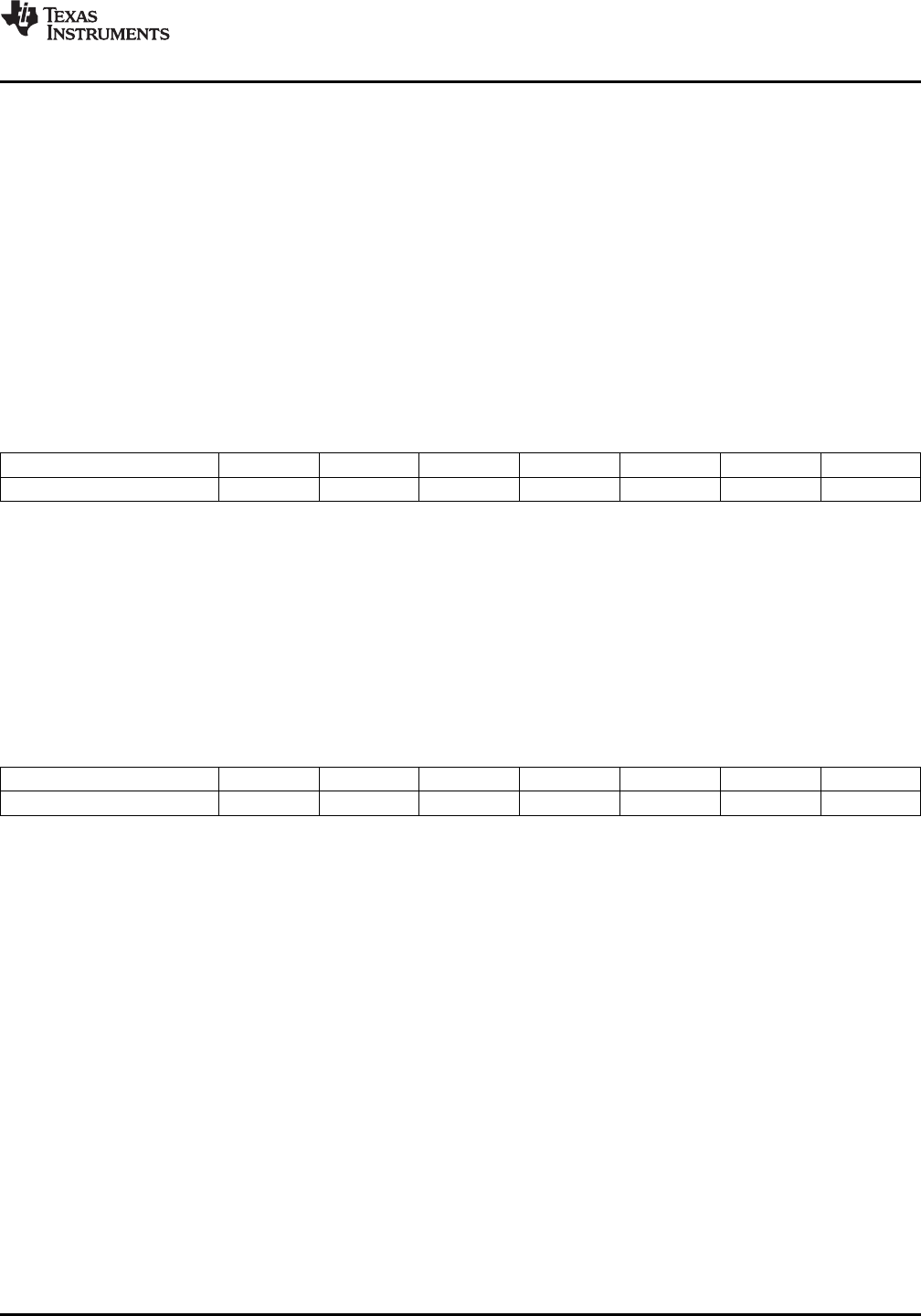
TRF7960
TRF7961
www.ti.com
SLOU186F–AUGUST 2006–REVISED AUGUST 2010
the RF and receivers are switched ON. When this command is received, the reader observes the digitized
receiver output. If more than two edges are observed in 100 μs, the window comparator voltage is
increased. The procedure is repeated until the number of edges (changes of logical state) of the digitized
reception signal is less than 2 (in 100 μs). The command can reduce the input sensitivity in 5-dB
increments up to 15 dB. This command ensures better operation in a noisy environment.
The gain setting is reset to maximum gain at EN = 0, POR = 1.
5.4.9 Test External RF (RSSI at RX input with TX OFF)
This command can be used in active mode when the RF receiver is switched ON, and the RF output is
switched OFF (bit B1=1 in the chip status register, rec-on. See Table 5-9). The level of the RF signal
received on the antenna is measured and displayed in the RSSI levels register. The relation between the
3-bit code and the external RF field strength [A/m] must be determined by calculation or by experiments
for each antenna design. The antenna Q and connection to the RF input influence the result. The nominal
relation between the RF peak-to-peak voltage at the receiver inputs and its corresponding RSSI level is
presented as follows.
Receiver Input [mVPP] 40 60 80 100 140 180 300
RSSI level 1 2 3 4 5 6 7
If the direct command test RF internal or test RF external is used immediately after activation, it should be
preceded with a command enable RX to activate the RX section. For proper execution of the test RF
commands, the RX section must be enabled. This happens automatically when a data exchange between
the reader and the tag is done, or by sending a direct command enable RX.
5.4.10 Test Internal RF (RSSI at RX input with TX ON)
This command measures the level of the RF carrier at the receive inputs. Its operating range is between
300 mVp and 2.1 Vp with a step size of 300 mV. The two values are displayed in the RSSI levels register.
The command is intended for diagnostic purposes to set the correct RX_IN levels. The optimum RX_IN
input level is approximately 1.6 Vp, or an RSSI level of 5 or 6. The nominal relationship between the input
RF peak level and the RSSI code is presented as follows.
Receiver Input [mVPp] 300 600 900 1200 1500 1800 2100
RSSI Level 1 2 3 4 5 6 7
5.4.11 Block Receiver
The block receiver command puts the digital part of receiver (bit decoder and framer) in reset mode. This
is useful in an extremely noisy environment, where the noise level could otherwise cause a constant
switching of the sub-carrier input of the digital part of the receiver. The receiver (if not in reset) would try to
catch a SOF signal, and if the noise pattern matched the SOF pattern, an interrupt would be generated,
falsely signaling the start of an RX operation. A constant flow of interrupt requests can be a problem for
the external system (MCU), so the external system can stop this by putting the receive decoders in reset
mode. The reset mode can be terminated in two ways. The external system can send the enable receiver
command. The reset mode is also automatically terminated at the end of a TX operation. The receiver can
stay in reset after end of TX if the RX wait time register (address 08) is set. In this case, the receiver is
enabled at the end of the wait time following the transmit operation.
5.4.12 Enable Receiver
This command clears the reset mode in the digital part of the receiver if the reset mode was entered by
the block receiver command.
Copyright ©2006–2010, Texas Instruments Incorporated System Description 35
Submit Documentation Feedback
focus.ti.com: TRF7960 TRF7961
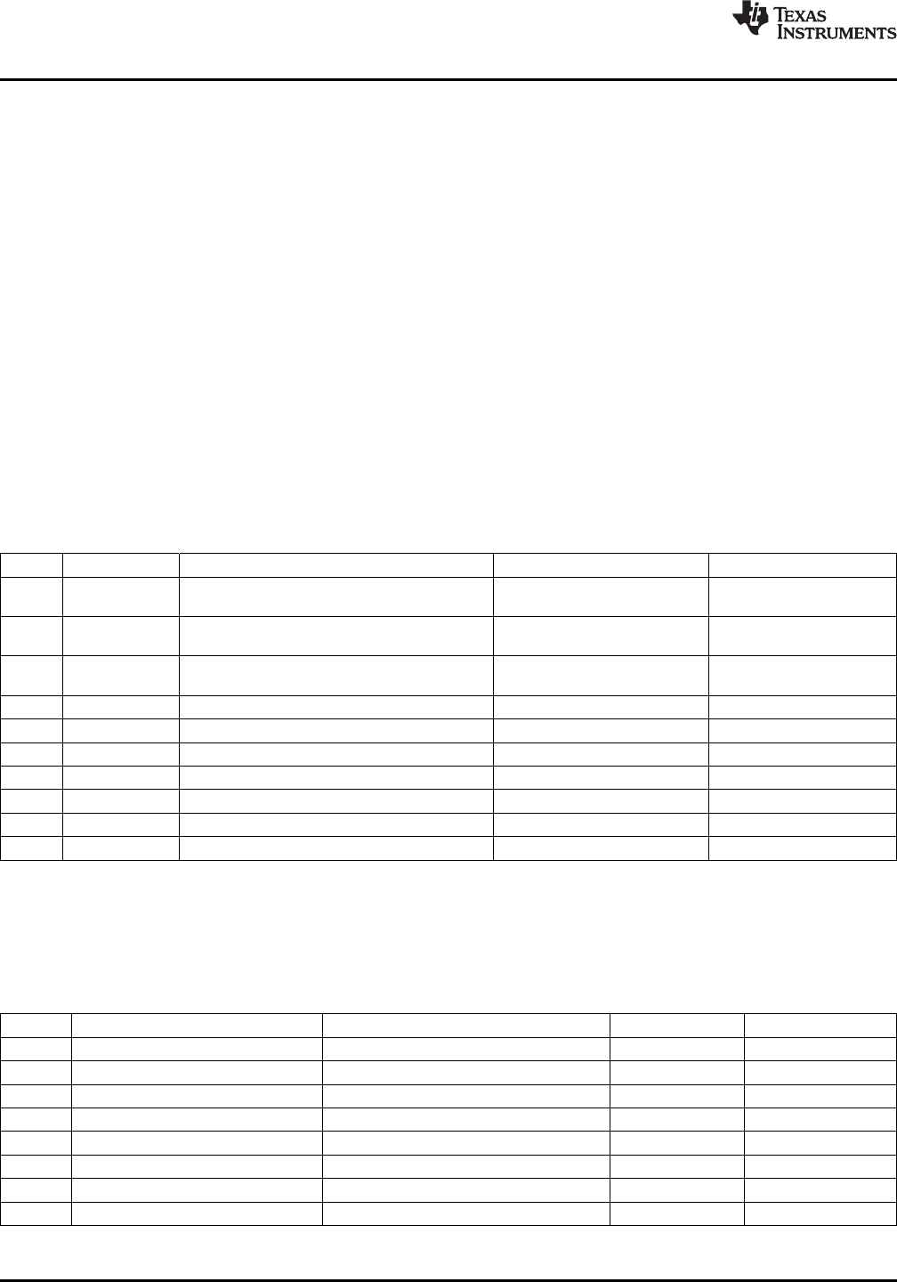
TRF7960
TRF7961
SLOU186F–AUGUST 2006–REVISED AUGUST 2010
www.ti.com
5.5 Reader Communication Interface
5.5.1 Introduction
The communication interface to the reader can be configured in two ways: a parallel 8-pin interface and a
Data_Clk or a serial peripheral interface (SPI).
These modes are mutually exclusive; only one mode can be used at a time in the application.
When the SPI interface is selected, the unused I/O_2, I/O_1, and I/O_0 pins must be hard-wired according
to Table 5-30. At power up, the reader samples the status of these three pins. If they are not the same (all
High or all Low) it enters one of the possible SPI modes.
The reader always behaves as the slave while the microcontroller (MCU) behaves as the master device.
The MCU initiates all communications with the reader and is also used to communicate with the higher
levels (application layer). The reader has an IRQ pin to prompt the MCU for attention if the reader detects
a response from the proximity/vicinity integrated circuit card (PICC/VICC).
Communication is initialized by a start condition, which is expected to be followed by an
Address/Command word (Adr/Cmd). The Adr/Cmd word is 8 bits long, and its format is shown in
Table 5-31.
Table 5-30. Pin Assignment in Parallel and Serial Interface Connection or Direct Mode
Pin Parallel Parallel-Direct SPI with SS SPI without SS
DATA_ DATA_CLK DATA_CLK DATA_CLK from master DATA_CLK from master
CLK
I/O_7 A/D[7] MOSI(1) = data-in (reader-in) MOSI(1) = data-in
(reader-in)
I/O_6 A/D[6] Direct mode, data out (sub-carrier or bit stream) MISO(2) = data-out (MCU-out) MISO(2) = data-out
(MCU-out)
I/O_5(3) A/D[5] Direct mode, strobe –bit clock out See Note 3 See Note 3
I/O_4 A/D[4] SS –slave select(4) —
I/O_3 A/D[3] — — —
I/O_2 A/D[2] —at VDD at VDD
I/O_1 A/D[1] —at VDD at VSS
I/O_0 A/D[0] —at VSS at VSS
IRQ IRQ interrupt IRQ interrupt IRQ interrupt IRQ interrupt
(1) MOSI –master out, slave in
(2) MISO –master in, slave out
(3) IO_5 pin is used only for information when data is put out of the chip (for example, reading 1 byte from the chip). It is necessary first to
write in the address of the register (8 clocks) and then to generate another 8 clocks for reading out the data. The IO_5 pin goes high in
this second 8 clocks. But for normal SPI operation this pin IO_5 is not used.
(4) Slave-select pin active-low
Table 5-31. Address/Command Word Bit Distribution
Bit Description Bit Function Address Command
Bit 7 Command control bit 0 = address, 1 = command 0 1
Bit 6 Read/Write 1 = read, 0 = write R/W 0
Bit 5 Continuous address mode 1 = Cont. mode R/W 0
Bit 4 Address/Command bit 4 Adr 4 Cmd 4
Bit 3 Address/Command bit 3 Adr 3 Cmd 3
Bit 2 Address/Command bit 2 Adr 2 Cmd 2
Bit 1 Address/Command bit 1 Adr 1 Cmd 1
Bit 0 Address/Command bit 0 Adr 0 Cmd 0
36 System Description Copyright ©2006–2010, Texas Instruments Incorporated
Submit Documentation Feedback
focus.ti.com: TRF7960 TRF7961
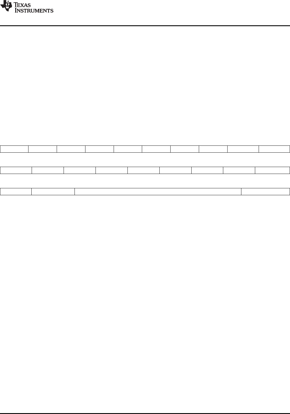
TRF7960
TRF7961
www.ti.com
SLOU186F–AUGUST 2006–REVISED AUGUST 2010
The MSB (bit 7) determines if the word is to be used as a command or as an address. The last two
columns of Table 5-31 show the function of the separate bits if either address or command is written. Data
is expected once the address word is sent. In continuous-address mode (Cont. mode = 1), the first data
that follows the address is written (or read) to (from) the given address. For each additional data, the
address is incremented by one. Continuous mode can be used to write to a block of control registers in a
single stream without changing the address; for example, setup of the predefined standard control
registers from the MCU’s non-volatile memory to the reader. In non-continuous address mode (simple
addressed mode), only one data word is expected after the address.
Address mode is used to write or read the configuration registers or the FIFO. When writing more than 12
bytes to the FIFO, the continuous address mode should be set to 1.
The command mode is used to enter a command resulting in reader action (initialize transmission, enable
reader, and turn reader On/Off...)
An example of expected communication between MCU and reader is shown below.
Continuous address mode
Start Adr x Data(x) Data(x+1) Data(x+2) Data(x+3) Data(x+4) ... Data(x+n) StopCont
Non-continuous address mode (single address mode)
Start Adr x Data(x) Adr y Data(y) ... Adr z Data(z) StopSgl
Command mode
Start Cmd x (Optional data or command) Stop
Copyright ©2006–2010, Texas Instruments Incorporated System Description 37
Submit Documentation Feedback
focus.ti.com: TRF7960 TRF7961
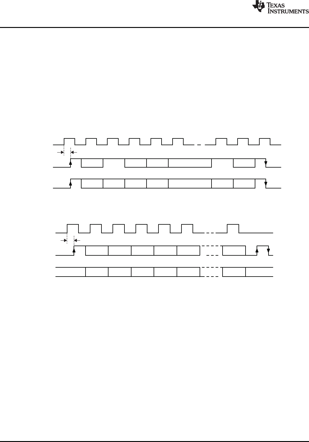
a1[7] d1[7] a2[7] d2[7] aN[7] dN[7]
Start
Condition
StopSmpl
Condition
CLK
I/O_[7]
I/O_[6:0]
a1[6:0] a2[6:0]d1[6:0] d2[6:0] aN[6:0] dN[6:0]
50ns
a0[7] d0[7]
Start
Condition
CLK
I/O_[7]
I/O_[6:0] a0[6:0] d0[6:0]xx d1[6:0] d2[6:0]
d2[7]
dN[6:0]d3[6:0]
dN[7]
xx
StopCont
ContinuousMode
d1[7] d3[7]
50ns
TRF7960
TRF7961
SLOU186F–AUGUST 2006–REVISED AUGUST 2010
www.ti.com
5.6 Parallel Interface Communication
In parallel mode, the start condition is generated on the rising edge of the I/O_7 pin while the CLK is high.
This is used to reset the interface logic. Figure 5-5 shows the sequence of the data, with an 8-bit address
word first, followed by data.
Communication is ended by:
•the StopSmpl condition, where the falling edge on the I/O_7 pin is expected while CLK is high
•the StopCont condition, where the I/O_7 pin must have a successive rising and falling edge while CLK
is low in order to reset the parallel interface and be ready for the new communication sequence
The StopSmpl condition is also used to terminate the direct mode.
Figure 5-5. Parallel Interface Communication With Simple Stop Condition StopSmpl
Figure 5-6. Parallel Interface Communication With Continuous Stop Condition StopCont
38 System Description Copyright ©2006–2010, Texas Instruments Incorporated
Submit Documentation Feedback
focus.ti.com: TRF7960 TRF7961
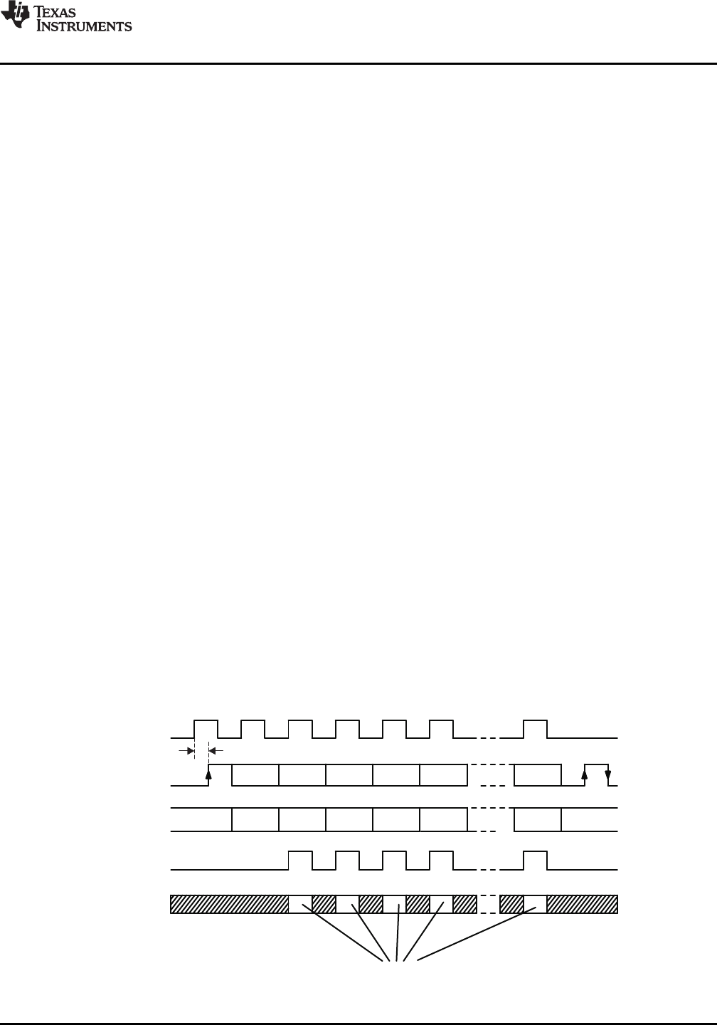
Start
Condition
CLK
I/O_[7]
I/O_[6:0]
a0[6:0]
d0[6:0]
xx
d1[6:0]
d2[6:0]
dN[6:0]
d3[6:0]
xx
StopCont
ValidOuputData
a0[7]
d0[7]
d2[7]
dN[7]
d1[7]
d3[7]
InternalOE
OutputData
50ns
TRF7960
TRF7961
www.ti.com
SLOU186F–AUGUST 2006–REVISED AUGUST 2010
5.6.1 Receive
At the start of a receive operation (when SOF is successfully detected), B6 is set in the IRQ status
register. An interrupt request is sent to the MCU at the end of the receive operation if the receive data
string was shorter than or equal to 8 bytes. The MCU receives the interrupt request, then checks to
determine the reason for the interrupt by reading the IRQ status register (address 0Ch), after which the
MCU reads the data from the FIFO.
If the received packet is longer than 8 bytes, the interrupt is sent before the end of the receive operation
when the ninth byte is loaded into the FIFO (75% full). The MCU should again read the content of the IRQ
status register to determine the cause of the interrupt request. If the FIFO is 75% full (as marked with flag
B5 in IRQ status register and by reading the FIFO status register), the MCU should respond by reading
the data from FIFO to make room for new incoming receive data. When the receive operation is finished,
the interrupt is sent and the MCU must check how many words are still present in the FIFO before it
finishes reading.
If the reader detects a receive error, the corresponding error flag is set (framing error, CRC error) in the
IRQ status register, which indicates that the MCU reception was completed incorrectly.
5.6.2 Transmit
Before beginning data transmission, the FIFO should be cleared with a reset command (0F). Data
transmission is initiated with a selected command (described in the Direct Commands section,
Table 5-29). The MCU then commands the reader to do a continuous write command (3Dh, see
Table 5-31) starting from register 1Dh. Data written into register 1Dh is the TX length byte1 (upper and
middle nibbles), while the following byte in register 1Eh is the TX length byte 2 (lower nibble and broken
byte length). Note that the TX byte length determines when the reader sends the EOF byte. After the TX
length bytes are written, FIFO data is loaded in register 1Fh with byte storage locations 0 to 11. Data
transmission begins automatically after the first byte is written into the FIFO. The loading of TX length
bytes and the FIFO can be done with a continuous-write command, as the addresses are sequential.
At the start of transmission, the flag B7 (Irq_tx) is set in the IRQ status register. If the transmit data is
shorter than or equal to 4 bytes, the interrupt is sent only at the end of the transmit operation. If the
number of bytes to be transmitted is higher or equal to 5, then the interrupt is generated. This occurs also
when the number of bytes in the FIFO reaches 3. The MCU should check the IRQ status register and
FIFO status register and then load additional data to the FIFO, if needed. At the end of the transmit
operation, an interrupt is sent to inform the MCU that the task is complete.
Figure 5-7. Data Output Only When CLK Is High
Copyright ©2006–2010, Texas Instruments Incorporated System Description 39
Submit Documentation Feedback
focus.ti.com: TRF7960 TRF7961
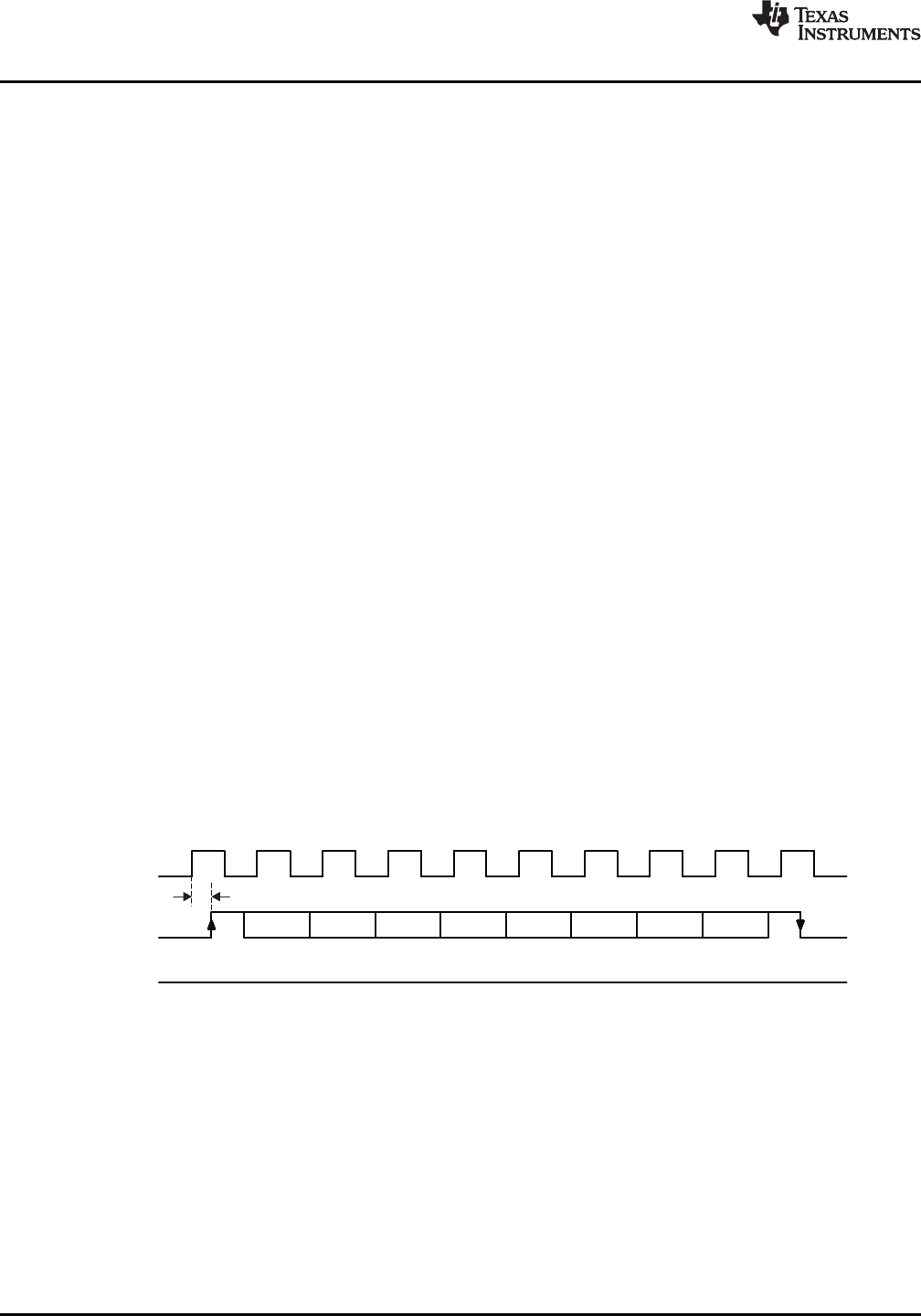
b7 b6 b5 b4 b3 b2 b1 b0
Start
Condition
Stop
Condition
SCLK
DataIN
DataOut
50ns
TRF7960
TRF7961
SLOU186F–AUGUST 2006–REVISED AUGUST 2010
www.ti.com
5.7 Serial Interface Communication
When an SPI interface is required, parallel I/O pins, I/O_2, I/O_1, and I/O_0, must be hard wired
according to Table 5-31. On power up, the reader looks for the status of these pins; if they are not the
same (not all high, or not all low), the reader enters into one of two possible SPI modes.
The serial communications work in the same manner as the parallel communications with respect to the
FIFO, except for the following condition. On receiving an IRQ from the reader, the MCU reads the reader's
IRQ register to determine how to service the reader. After this, the MCU must to do a dummy read to clear
the reader's IRQ status register. The dummy read is required in SPI mode because the reader's IRQ
status register needs an additional clock cycle to clear the register. This is not required in parallel mode
because the additional clock cycle is included in the Stop condition.
A procedure for a dummy read is as follows:
A. Starting the dummy read:
(a) When using slave select (SS): set SS bit low.
(b) When not using SS: start condition is when SCLK is high (See Table 5-30).
B. Send address word to IRQ status register (0Ch) with read and continuous address mode bits set to 1
(See Table 5-31).
C. Read 1 byte (8 bits) from IRQ status register (0Ch).
D. Dummy-read 1 byte from register 0Dh (collision position and interrupt mask).
E. Stopping the dummy read:
(a) When using slave select (SS): set SS bit high.
(b) When not using SS: stop condition when SCLK is high (See Table 5-30).
5.7.1 SPI Interface Without SS* (Slave Select) Pin
The serial interface without the slave select pin must use delimiters for the start and stop conditions.
Between these delimiters, the address, data, and command words can be transferred. All words must be 8
bits long with MSB transmitted first.
Figure 5-8. Serial –SPI Interface Communication (No SS* Pin)
In this mode, a rising edge on data-in (I/O_7, pin 24) while SCLK is high resets the serial interface and
prepares it to receive data. Data-in can change only when SCLK is low and is taken by the reader on the
SCLK rising edge. Communication is terminated by the stop condition when the data-in falling edge occurs
during a high SCLK period.
5.7.2 SPI Interface With SS* (Slave Select) Pin
The serial interface is in reset while the SS* signal is high. Serial data-in (MOSI) changes on the falling
edge, and is validated in the reader on the rising edge, as shown in Figure 5-9. Communication is
terminated when the SS* signal goes high.
All words must be 8 bits long with the MSB transmitted first.
40 System Description Copyright ©2006–2010, Texas Instruments Incorporated
Submit Documentation Feedback
focus.ti.com: TRF7960 TRF7961
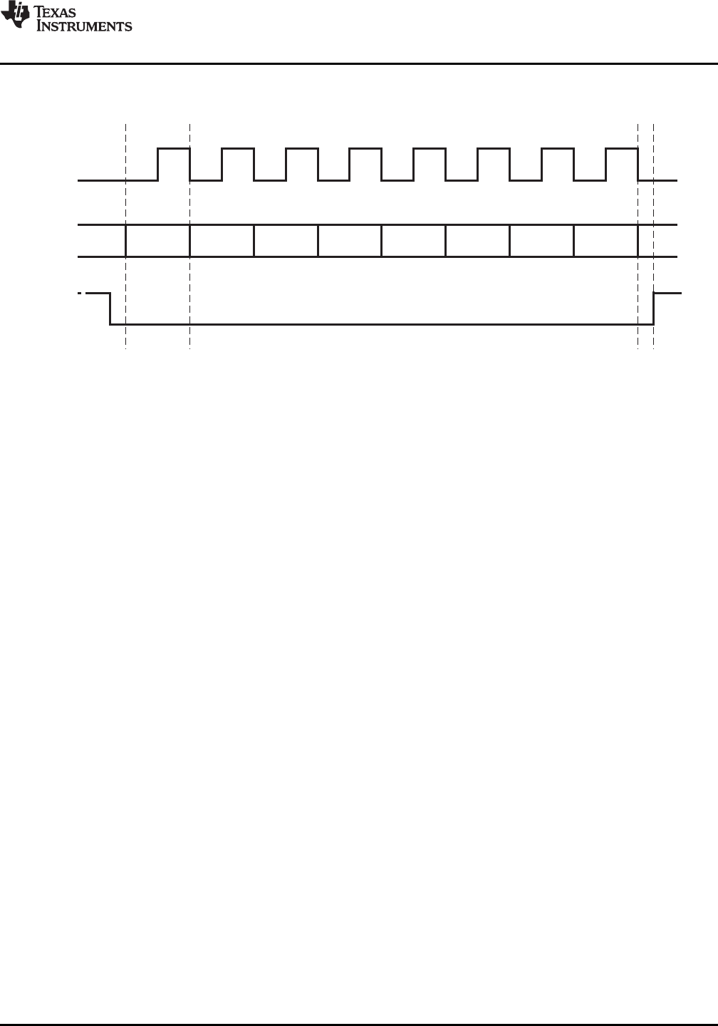
SCLK
MOSI
SS*
B7 B6 B5 B4 B3 B2 B1 B0
WriteOperation
TRF7960
TRF7961
www.ti.com
SLOU186F–AUGUST 2006–REVISED AUGUST 2010
Figure 5-9. Serial–SPI Interface Communication (Write Mode)
Copyright ©2006–2010, Texas Instruments Incorporated System Description 41
Submit Documentation Feedback
focus.ti.com: TRF7960 TRF7961
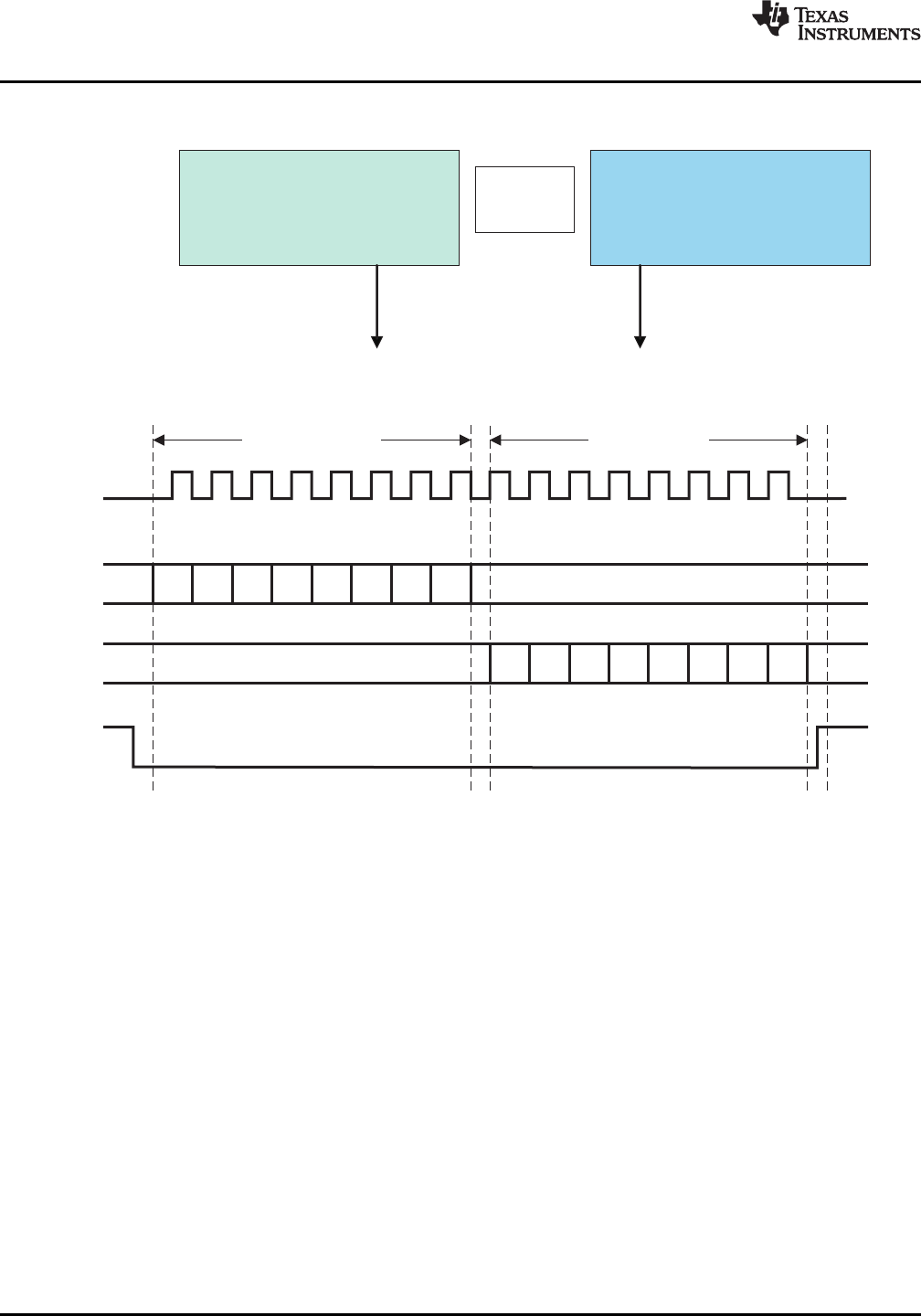
WriteMode
CKPH – 1,CKPL – 0(MSP430)
Data Transition – SCLKFallingEdge
MOSIValid – SCLKRisingEdge
Switch
SCLK
Polarity
ReadMode
CKPH – 0,CKPL – 0(MSP430)
Data Transition – SCLKRisingEdge
MISOValid – SCLKFallingEdge
SingleReadOperation
SCLK
MOSI
MISO
SS*
Write AddressByte ReadDataByte
B7
B7
B6
B6
B5
B5
B4
B4
B3
B3
B2
B2
B1
B1
B0
B0
Don'tCare
NoData Transitions(AllHigh/Low)
TRF7960
TRF7961
SLOU186F–AUGUST 2006–REVISED AUGUST 2010
www.ti.com
The SPI read operation is shown in Figure 5-10.
Figure 5-10. Serial –SPI Interface Communication (Read Mode)
The read command is sent out on the MOSI pin, MSB first, in the first eight clock cycles. MOSI data
changes on the falling edge, and is validated in the reader on the rising edge, as shown in Figure 5-10.
During the write cycle, the serial data out (MISO) is not valid. After the last read command bit (B0) is
validated at the eighth rising edge of SCLK, after half a clock cycle, valid data can be read on the MISO
pin at the falling edge of SCLK. It takes eight clock edges to read out the full byte (MSB first).
Note:
When using the hardware SPI (for example, an MSP430 hardware SPI) to implement the foregoing
feature, care must be taken to switch the SCLK polarity after write phase for proper read operation.
The example clock polarity for the MSP430-specific environment is shown in the write-mode and
read-mode boxes of Figure 5-10. See the USART-SPI chapter for any specific microcontroller family
for further information on the setting the appropriate clock polarity.
This clock polarity switch must be done for all read (single, continuous) operations.
The MOSI (serial data out) should not have any transitions (all high or all low) during the read cycle. Also,
the SS* should be low during the whole write and read operation.
The continuous read operation is illustrated in Figure 5-11
42 System Description Copyright ©2006–2010, Texas Instruments Incorporated
Submit Documentation Feedback
focus.ti.com: TRF7960 TRF7961
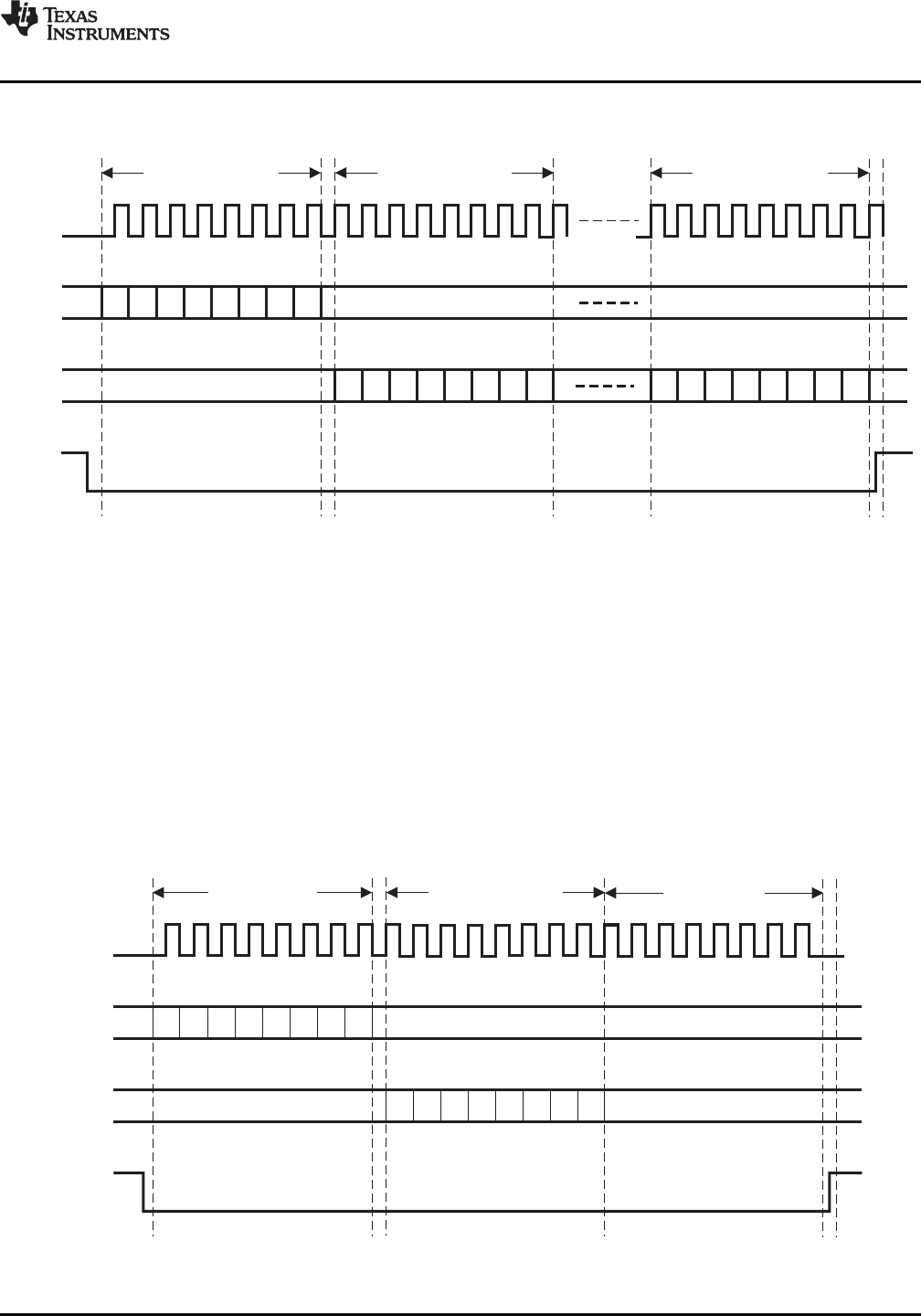
MOSI
MISO
SS*
SCLK
B0
B0 B0
B7
B7 B7
B6
B6 B6
B5
B5 B5
B4
B4 B4
B3
B3 B3
B2
B2 B2
B1
B1 B1
No Data Transitions (All High/Low) No Data Transitions (All High/Low)
Don’t Care
ContinuousReadOperation
Write Address Byte Read Data Byte 1 Read Data Byte n
MOSI
MISO
SS*
SCLK
B0
B0
B7
B7
B6
B6
B5
B5
B4
B4
B3
B3
B2
B2
B1
B1
No Data Transitions (All High/Low) No Data Transitions (All High/Low)
Don’t Care Ignore
SpecialCase – IRQStatusRegisterRead
Dummy Read
ReadDatain
IRQStatusRegister
Write Address
Byte(0x6C)
TRF7960
TRF7961
www.ti.com
SLOU186F–AUGUST 2006–REVISED AUGUST 2010
Figure 5-11. SPI Interface Communication (Continuous Read Mode)
Note:
Special steps are needed to read the TRF796x IRQ status register (register address 0x0C) in SPI mode.
The status of the bits in this register is cleared after a dummy read. The following steps must be followed
when reading the “IRQ status register”.
1. Write in command 0x6C: read 'IRQ status' register in continuous mode (eight clocks).
2. Read out the data in register 0x0C (eight clocks).
3. Generate another eight clocks (as if reading the data in register 0x0D) but ignore the MISO data line.
This is shown in Figure 5-12.
Figure 5-12. SPI Interface Communication (IRQ Status Register Read)
Copyright ©2006–2010, Texas Instruments Incorporated System Description 43
Submit Documentation Feedback
focus.ti.com: TRF7960 TRF7961

TRF7960
TRF7961
SLOU186F–AUGUST 2006–REVISED AUGUST 2010
www.ti.com
5.7.2.1 FIFO Operation
The FIFO is a 12-byte register at address 1Fh with byte storage locations 0 to 11. FIFO data is loaded in a
cyclical manner and can be cleared by a reset command (0F).
Associated with the FIFO are two counters and three FIFO status flags. The first counter is a 4-bit FIFO
byte counter (bits B0–B3 in register 1Ch) that keeps track of the number of bytes loaded into the FIFO. If
the number of bytes in the FIFO is n, the register value is n –1 (number of bytes in FIFO register). If 8
bytes are in the FIFO, the FIFO counter (bits B0–B3 in register 1Ch) has the value 7.
A second counter (12 bits wide) indicates the number of bytes being transmitted (registers 1Dh and 1Eh)
in a data frame. An extension to the transmission-byte counter is a 4-bit broken-byte counter also provided
in register 1Eh (bits B0-B3). Together these counters make up the TX length value that determines when
the reader generates the EOF byte.
FIFO status flags are as follows:
1. FIFO overflow (bit B4 of register 1Ch) –indicates that the FIFO was loaded too soon
2. FIFO level too low (bit B5 of register 1Ch) –indicates that only three bytes are left to be transmitted
(Can be used during transmission)
3. FIFO level high (bit B6 of register 1Ch) –indicates that nine bytes are already loaded into the FIFO
(Can be used during reception to generate a FIFO reception IRQ. This is to notify the MCU to service
the reader in time to ensure a continuous data stream.)
During transmission, the FIFO is checked for an almost-empty condition, and during reception for an
almost-full condition. The maximum number of bytes that can be loaded into the FIFO in a single
sequence is 12 bytes. (Note: The number of bytes in a frame, transmitted or received, can be greater than
12 bytes.)
During transmission, the MCU loads the reader's FIFO (or during reception the MCU removes data from
the FIFO), and the FIFO counter counts the number of bytes being loaded into the FIFO. Meanwhile, the
byte counter keeps track of the number of bytes being transmitted. An interrupt request is generated if the
number of bytes in the FIFO is less than 3 or greater than 9, so that MCU can send new data or remove
the data as necessary. The MCU also checks the number of data bytes to be sent, so as to not surpass
the value defined in TX length bytes. The MCU also signals the transmit logic when the last byte of data is
sent or was removed from the FIFO during reception. Transmission starts automatically after the first byte
is written into FIFO.
5.8 External Power Amplifier Application
Applications requiring an extended read range can use an external power amplifier together with the
TRF7960/61. This can be implemented by adding an external power amplifier on the transmit side and
external sub-carrier detectors on the receive side.
To implement the external power amplification feature, certain registers must be programmed as shown
below.
1. Set bit B6 of the Regulator and I/O Control register to 1 (see Table 5-21).
This setting has two functions, first to provide a modulated signal for the transmitter if needed, and
second to configure the TRF7960/61 receiver inputs for an external demodulated sub-carrier input.
2. Set bit B3 of the modulation and SYS_CLK control register to 1 (see Table 5-19).
This function configures the ASK / OOK pin for either a digital or analog output (B3 = 0 enables a
digital output, B3 = 1 enables an analog output).
44 System Description Copyright ©2006–2010, Texas Instruments Incorporated
Submit Documentation Feedback
focus.ti.com: TRF7960 TRF7961
PACKAGE OPTION ADDENDUM
www.ti.com 25-Jul-2012
Addendum-Page 1
PACKAGING INFORMATION
Orderable Device Status (1) Package Type Package
Drawing Pins Package Qty Eco Plan (2) Lead/
Ball Finish MSL Peak Temp (3) Samples
(Requires Login)
TRF7960RHBR ACTIVE QFN RHB 32 3000 Green (RoHS
& no Sb/Br)
CU NIPDAU Level-2-260C-1 YEAR
TRF7960RHBT ACTIVE QFN RHB 32 250 Green (RoHS
& no Sb/Br)
CU NIPDAU Level-2-260C-1 YEAR
TRF7961RHBR ACTIVE QFN RHB 32 3000 Green (RoHS
& no Sb/Br)
CU NIPDAU Level-2-260C-1 YEAR
TRF7961RHBT ACTIVE QFN RHB 32 250 Green (RoHS
& no Sb/Br)
CU NIPDAU Level-2-260C-1 YEAR
(1) The marketing status values are defined as follows:
ACTIVE: Product device recommended for new designs.
LIFEBUY: TI has announced that the device will be discontinued, and a lifetime-buy period is in effect.
NRND: Not recommended for new designs. Device is in production to support existing customers, but TI does not recommend using this part in a new design.
PREVIEW: Device has been announced but is not in production. Samples may or may not be available.
OBSOLETE: TI has discontinued the production of the device.
(2) Eco Plan - The planned eco-friendly classification: Pb-Free (RoHS), Pb-Free (RoHS Exempt), or Green (RoHS & no Sb/Br) - please check http://www.ti.com/productcontent for the latest availability
information and additional product content details.
TBD: The Pb-Free/Green conversion plan has not been defined.
Pb-Free (RoHS): TI's terms "Lead-Free" or "Pb-Free" mean semiconductor products that are compatible with the current RoHS requirements for all 6 substances, including the requirement that
lead not exceed 0.1% by weight in homogeneous materials. Where designed to be soldered at high temperatures, TI Pb-Free products are suitable for use in specified lead-free processes.
Pb-Free (RoHS Exempt): This component has a RoHS exemption for either 1) lead-based flip-chip solder bumps used between the die and package, or 2) lead-based die adhesive used between
the die and leadframe. The component is otherwise considered Pb-Free (RoHS compatible) as defined above.
Green (RoHS & no Sb/Br): TI defines "Green" to mean Pb-Free (RoHS compatible), and free of Bromine (Br) and Antimony (Sb) based flame retardants (Br or Sb do not exceed 0.1% by weight
in homogeneous material)
(3) MSL, Peak Temp. -- The Moisture Sensitivity Level rating according to the JEDEC industry standard classifications, and peak solder temperature.
Important Information and Disclaimer:The information provided on this page represents TI's knowledge and belief as of the date that it is provided. TI bases its knowledge and belief on information
provided by third parties, and makes no representation or warranty as to the accuracy of such information. Efforts are underway to better integrate information from third parties. TI has taken and
continues to take reasonable steps to provide representative and accurate information but may not have conducted destructive testing or chemical analysis on incoming materials and chemicals.
TI and TI suppliers consider certain information to be proprietary, and thus CAS numbers and other limited information may not be available for release.
In no event shall TI's liability arising out of such information exceed the total purchase price of the TI part(s) at issue in this document sold by TI to Customer on an annual basis.
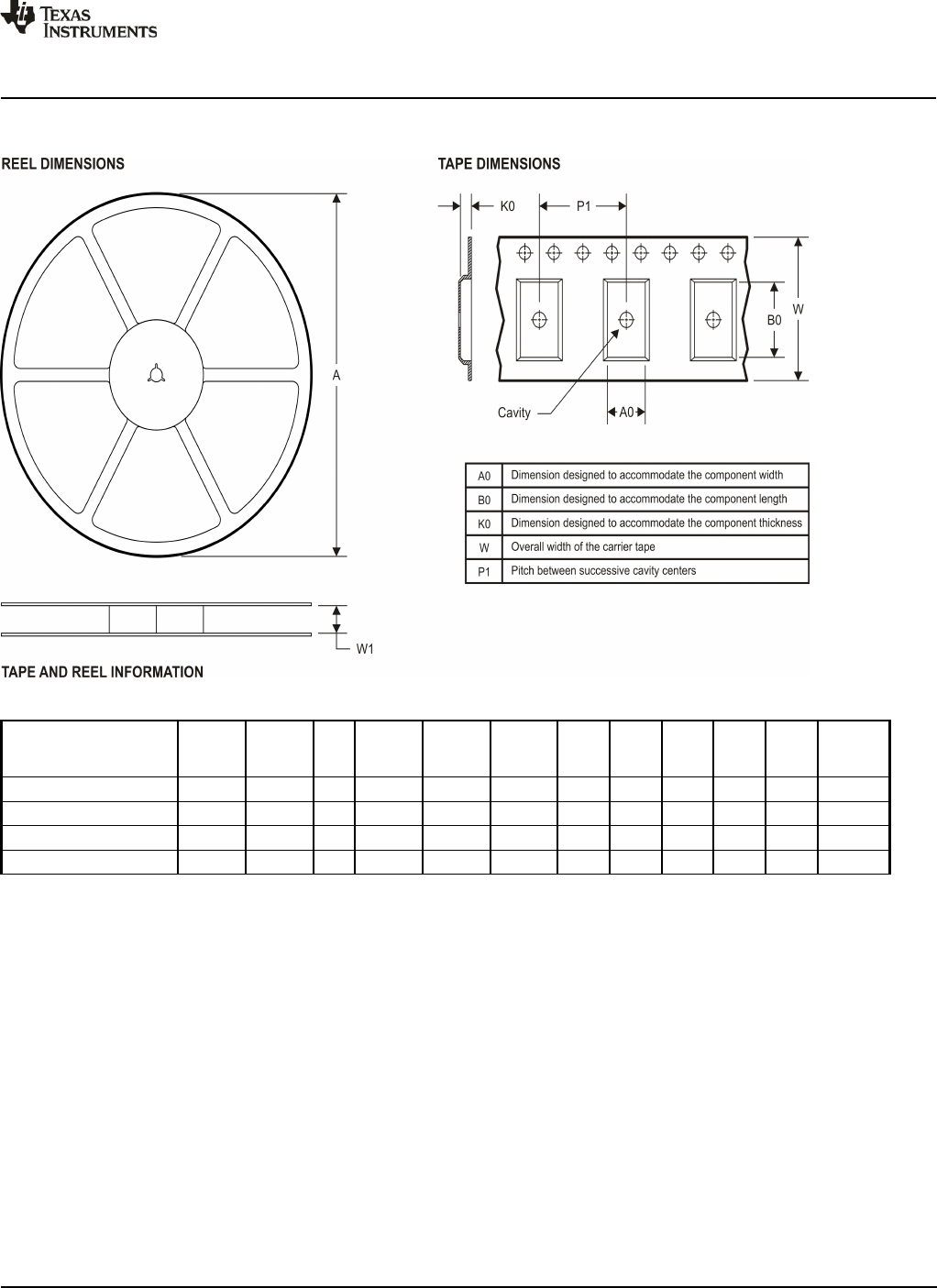
TAPE AND REEL INFORMATION
*All dimensions are nominal
Device Package
Type Package
Drawing Pins SPQ Reel
Diameter
(mm)
Reel
Width
W1 (mm)
A0
(mm) B0
(mm) K0
(mm) P1
(mm) W
(mm) Pin1
Quadrant
TRF7960RHBR QFN RHB 32 3000 330.0 12.4 5.3 5.3 1.5 8.0 12.0 Q2
TRF7960RHBT QFN RHB 32 250 180.0 12.4 5.3 5.3 1.5 8.0 12.0 Q2
TRF7961RHBR QFN RHB 32 3000 330.0 12.4 5.3 5.3 1.5 8.0 12.0 Q2
TRF7961RHBT QFN RHB 32 250 180.0 12.4 5.3 5.3 1.5 8.0 12.0 Q2
PACKAGE MATERIALS INFORMATION
www.ti.com 14-Jul-2012
Pack Materials-Page 1
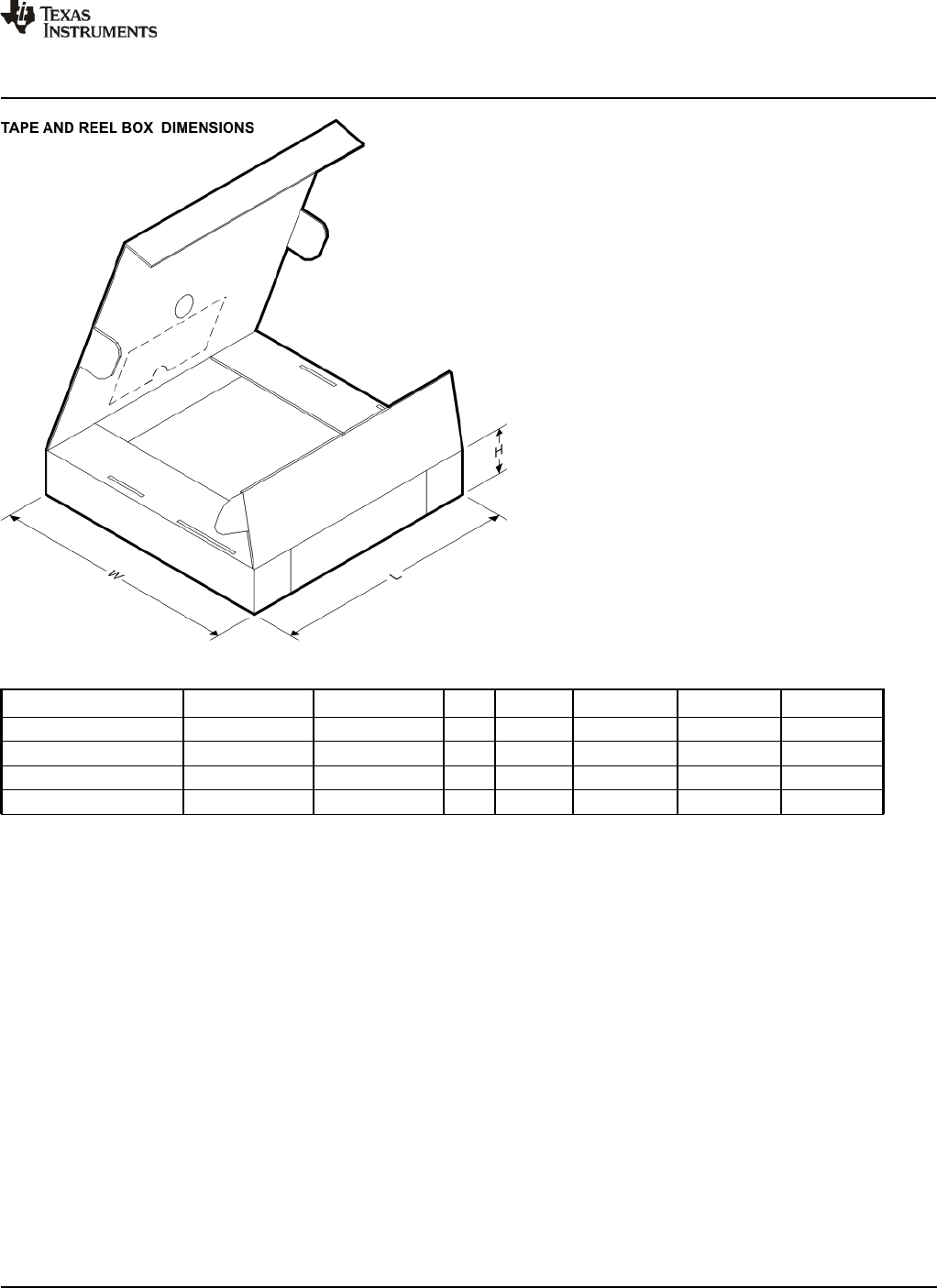
*All dimensions are nominal
Device Package Type Package Drawing Pins SPQ Length (mm) Width (mm) Height (mm)
TRF7960RHBR QFN RHB 32 3000 367.0 367.0 35.0
TRF7960RHBT QFN RHB 32 250 210.0 185.0 35.0
TRF7961RHBR QFN RHB 32 3000 367.0 367.0 35.0
TRF7961RHBT QFN RHB 32 250 210.0 185.0 35.0
PACKAGE MATERIALS INFORMATION
www.ti.com 14-Jul-2012
Pack Materials-Page 2
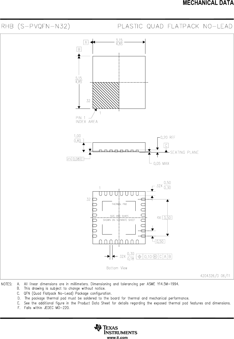
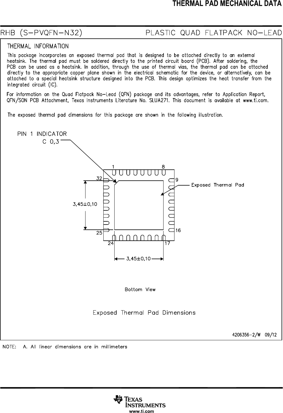
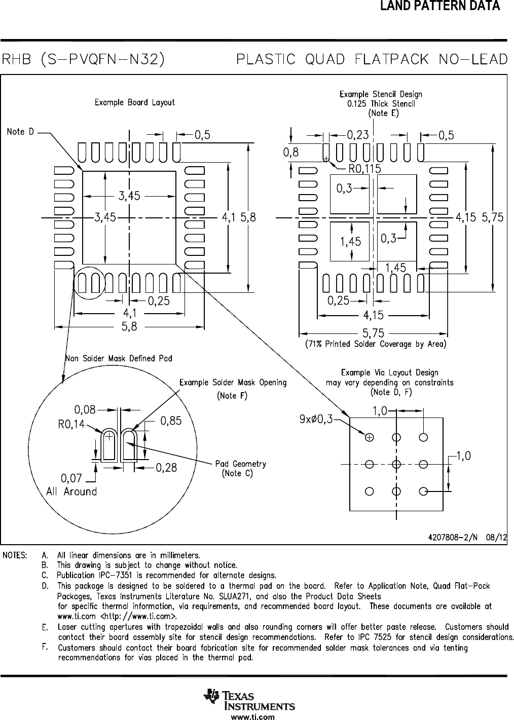

IMPORTANT NOTICE
Texas Instruments Incorporated and its subsidiaries (TI) reserve the right to make corrections, enhancements, improvements and other
changes to its semiconductor products and services per JESD46, latest issue, and to discontinue any product or service per JESD48, latest
issue. Buyers should obtain the latest relevant information before placing orders and should verify that such information is current and
complete. All semiconductor products (also referred to herein as “components”) are sold subject to TI’s terms and conditions of sale
supplied at the time of order acknowledgment.
TI warrants performance of its components to the specifications applicable at the time of sale, in accordance with the warranty in TI’s terms
and conditions of sale of semiconductor products. Testing and other quality control techniques are used to the extent TI deems necessary
to support this warranty. Except where mandated by applicable law, testing of all parameters of each component is not necessarily
performed.
TI assumes no liability for applications assistance or the design of Buyers’ products. Buyers are responsible for their products and
applications using TI components. To minimize the risks associated with Buyers’ products and applications, Buyers should provide
adequate design and operating safeguards.
TI does not warrant or represent that any license, either express or implied, is granted under any patent right, copyright, mask work right, or
other intellectual property right relating to any combination, machine, or process in which TI components or services are used. Information
published by TI regarding third-party products or services does not constitute a license to use such products or services or a warranty or
endorsement thereof. Use of such information may require a license from a third party under the patents or other intellectual property of the
third party, or a license from TI under the patents or other intellectual property of TI.
Reproduction of significant portions of TI information in TI data books or data sheets is permissible only if reproduction is without alteration
and is accompanied by all associated warranties, conditions, limitations, and notices. TI is not responsible or liable for such altered
documentation. Information of third parties may be subject to additional restrictions.
Resale of TI components or services with statements different from or beyond the parameters stated by TI for that component or service
voids all express and any implied warranties for the associated TI component or service and is an unfair and deceptive business practice.
TI is not responsible or liable for any such statements.
Buyer acknowledges and agrees that it is solely responsible for compliance with all legal, regulatory and safety-related requirements
concerning its products, and any use of TI components in its applications, notwithstanding any applications-related information or support
that may be provided by TI. Buyer represents and agrees that it has all the necessary expertise to create and implement safeguards which
anticipate dangerous consequences of failures, monitor failures and their consequences, lessen the likelihood of failures that might cause
harm and take appropriate remedial actions. Buyer will fully indemnify TI and its representatives against any damages arising out of the use
of any TI components in safety-critical applications.
In some cases, TI components may be promoted specifically to facilitate safety-related applications. With such components, TI’s goal is to
help enable customers to design and create their own end-product solutions that meet applicable functional safety standards and
requirements. Nonetheless, such components are subject to these terms.
No TI components are authorized for use in FDA Class III (or similar life-critical medical equipment) unless authorized officers of the parties
have executed a special agreement specifically governing such use.
Only those TI components which TI has specifically designated as military grade or “enhanced plastic” are designed and intended for use in
military/aerospace applications or environments. Buyer acknowledges and agrees that any military or aerospace use of TI components
which have not been so designated is solely at the Buyer's risk, and that Buyer is solely responsible for compliance with all legal and
regulatory requirements in connection with such use.
TI has specifically designated certain components which meet ISO/TS16949 requirements, mainly for automotive use. Components which
have not been so designated are neither designed nor intended for automotive use; and TI will not be responsible for any failure of such
components to meet such requirements.
Products Applications
Audio www.ti.com/audio Automotive and Transportation www.ti.com/automotive
Amplifiers amplifier.ti.com Communications and Telecom www.ti.com/communications
Data Converters dataconverter.ti.com Computers and Peripherals www.ti.com/computers
DLP® Products www.dlp.com Consumer Electronics www.ti.com/consumer-apps
DSP dsp.ti.com Energy and Lighting www.ti.com/energy
Clocks and Timers www.ti.com/clocks Industrial www.ti.com/industrial
Interface interface.ti.com Medical www.ti.com/medical
Logic logic.ti.com Security www.ti.com/security
Power Mgmt power.ti.com Space, Avionics and Defense www.ti.com/space-avionics-defense
Microcontrollers microcontroller.ti.com Video and Imaging www.ti.com/video
RFID www.ti-rfid.com
OMAP Applications Processors www.ti.com/omap TI E2E Community e2e.ti.com
Wireless Connectivity www.ti.com/wirelessconnectivity
Mailing Address: Texas Instruments, Post Office Box 655303, Dallas, Texas 75265
Copyright © 2012, Texas Instruments Incorporated
Federal Communication Commission Interference Statement
This device complies with Part 15 of the FCC Rules. Operation is subject to the
following two conditions: (1) This device may not cause harmful interference, and (2)
this device must accept any interference received, including interference that may
cause undesired operation.
This equipment has been tested and found to comply with the limits for a Class B
digital device, pursuant to Part 15 of the FCC Rules. These limits are designed to
provide reasonable protection against harmful interference in a residential installation.
This equipment generates, uses and can radiate radio frequency energy and, if not
installed and used in accordance with the instructions, may cause harmful interference
to radio communications. However, there is no guarantee that interference will not
occur in a particular installation. If this equipment does cause harmful interference
to radio or television reception, which can be determined by turning the equipment off
and on, the user is encouraged to try to correct the interference by one of the
following measures:
- Reorient or relocate the receiving antenna.
- Increase the separation between the equipment and receiver.
- Connect the equipment into an outlet on a circuit different from that
to which the receiver is connected.
- Consult the dealer or an experienced radio/TV technician for help.
FCC Caution: Any changes or modifications not expressly approved by the party
responsible for compliance could void the user's authority to operate this equipment.
This transmitter must not be co-located or operating in conjunction with any other
antenna or transmitter.

Radiation Exposure Statement:
The product is a low power device and its output power is lower than FCC SAR
exemption level. This module can be used with Getac PDA: PS336.
This device is intended only for OEM integrators under the following conditions:
1) The transmitter module may not be co-located with any other transmitter or
antenna. The co-transmitting with other radio will need a separate evaluation.
2) Module approval valid only when this module is installed in the tested host “Getac
PDA: PS336”.
As long as 2 conditions above are met, further transmitter test will not be required.
However, the OEM integrator is still responsible for testing their end-product for any
additional compliance requirements required with this module installed
IMPORTANT NOTE: In the event that these conditions cannot be met (for example
certain laptop configurations or co-location with another transmitter), then the FCC
authorization is no longer considered valid and the FCC ID cannot be used on the
final product. In these circumstances, the OEM integrator will be responsible for
re-evaluating the end product (including the transmitter) and obtaining a separate FCC
authorization.
End Product Labeling
The final end product must be labeled in a visible area with the following: “Contains
FCC ID: QYLPS336R”. The grantee's FCC ID can be used only when all FCC
compliance requirements are met.
Manual Information To the End User
The OEM integrator has to be aware not to provide information to the end user
regarding how to install or remove this RF module in the user’s manual of the end
product which integrates this module.
The end user manual shall include all required regulatory information/warning as
show in this manual.