Getac Technology RS500 UHF RFID Module User Manual module
Getac Technology Corporation UHF RFID Module module
Contents
- 1. User Manual-Host
- 2. User Manual-module
User Manual-module
Indy® RS500 Overview
Indy RS500 is a completely integrated UHF reader SiP
(system-in-package). It can be easily added to an
embedded system, requiring only connections to a power
source, digital communication with a host, and an
antenna. The package design allows it to be attached to a
PCB using standard surface mount technology (SMT),
with no need for additional connectors or mounting
hardware. The Indy RS500 is the easiest way to embed
UHF RFID reader capability.
Air Interface
Protocol
EPCglobal UHF Class 1 Gen 2 / ISO 18000-63 (formerly 18000-6C)
Supports dense reader mode (DRM)
Tx Output Power
+10 to +23 dBm (Peak Power)
Operating
Frequencies
IPJ-RS500-GX (902-928MHz) supports all 900MHz bands worldwide
IPJ-RS500-EU (865-868MHz) supports current EU operating band
Package
29 mm by 32 mm by 3.8 mm
Package Type
32 pin surface mount package (SMT compatible)
Rx Sensitivity
-65 dBm (1% packet error rate). Assumes a 15 dB antenna return loss at 23 dBm
output power.
DC Power Supply
3.6 to 5.25 Volts
Supported
Regions
Worldwide regional support. All major regions supported. See section 5.6 for a
complete list.
Compliance
Certified: FCC and Canada modular operation, RoHS compliant
For technical support, visit the Impinj support portal at support.impinj.com
Revision 1.1
www.impinj.com
Copyright © 2014, Impinj, Inc.
Impinj and Indy are either registered
trademarks or trademarks of Impinj, Inc.
For more information, contact readerchips@impinj.com
Indy® RS500 Datasheet
IPJ-RS500-GX, IPJ-RS500-EU
Electrical, Mechanical, & Thermal Specification
2
Revision 1.1, Copyright © 2014, Impinj, Inc.
1 Table of Contents
INDY® RS500 OVERVIEW .......................................................................................................................... 1
1
TABLE OF CONTENTS ......................................................................................................................... 2
1.1
FIGURES ............................................................................................................................................ 2
1.2
TABLES .............................................................................................................................................. 2
2
INTRODUCTION .................................................................................................................................... 3
2.1
KEY FEATURES OF THE INDY RS500 .................................................................................................... 4
3
SYSTEM BLOCK DIAGRAM ................................................................................................................. 4
4
PIN LISTING AND SIGNAL DEFINITIONS ........................................................................................... 7
5
ELECTRICAL SPECIFICATIONS ......................................................................................................... 8
5.1
ABSOLUTE MAXIMUM RATINGS ............................................................................................................ 8
5.2
OPERATING CONDITIONS ..................................................................................................................... 9
5.3
DEVICE FUNCTIONAL SPECIFICATIONS ................................................................................................. 9
5.4
UHF GEN 2 RFID RADIO SPECIFICATIONS ......................................................................................... 10
5.5
DEVICE INPUT AND OUTPUT SPECIFICATIONS ..................................................................................... 11
5.6
SUPPORTED REGIONS....................................................................................................................... 13
5.7
EPC CLASS-1 GENERATION-2 OPERATION ........................................................................................ 15
6
IMPINJ RADIO INTERFACE (IRI) ....................................................................................................... 16
7
REGULATORY INFORMATION .......................................................................................................... 17
8
PACKAGE AND ASSEMBLY INFORMATION ................................................................................... 17
8.1
PACKAGE MASS ................................................................................................................................ 17
8.2
PACKAGE DIMENSIONS ...................................................................................................................... 17
8.3
PCB FOOTPRINT .............................................................................................................................. 20
8.4
SMT REFLOW INFORMATION ............................................................................................................. 24
9
DOCUMENT CHANGE LOG ............................................................................................................... 25
10
NOTICES .......................................................................................................................................... 25
1.1 Figures
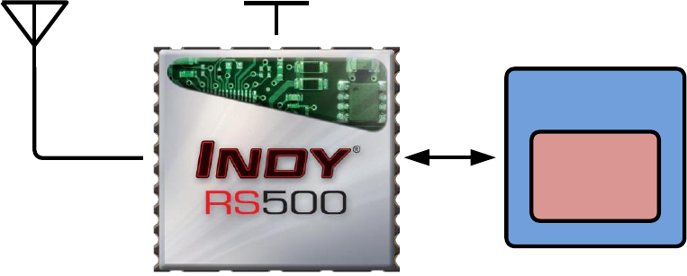
FIGURE 2-1: RS500 SYSTEM INTEGRATION ...................................................................................................... 4
FIGURE 3-1: EXAMPLE RS500 BLOCK DIAGRAM ............................................................................................... 5
FIGURE 4-1: INDY RS500 PIN LISTING .............................................................................................................. 7
FIGURE 6-1: HOST AND READER FIRMWARE STACK ........................................................................................ 16
FIGURE 8-1: RS500 PACKAGE DIMENSIONS, TOP, FRONT, AND SIDE VIEWS .................................................... 18
FIGURE 8-2: RS500 PIN DIMENSIONS (VIEWED FROM UNDERNEATH PACKAGE) ................................................. 19
FIGURE 8-3: RS500 RECOMMENDED ETCHED COPPER FOOTPRINT – ALL PADS .............................................. 20
FIGURE 8-4: RS500 RECOMMENDED ETCHED COPPER FOOTPRINT – SINGLE PAD ........................................... 21
FIGURE 8-5: RS500 RECOMMENDED PASTEMASK FOOTPRINT – ALL PADS ...................................................... 22
FIGURE 8-6: RS500 RECOMMENDED PASTEMASK FOOTPRINT – SINGLE PAD .................................................. 23
FIGURE 8-7: RECOMMENDED SOLDER STENCIL OPENING WITH ETCHED PAD FOR RS500 ................................. 23
FIGURE 8-8: RECOMMENDED SOLDER REFLOW PROFILE FOR THE INDY RS500 ............................................... 24
1.2 Tables
TABLE 4-1: INDY RS500 – PIN LISTING AND SIGNAL DEFINITIONS ...................................................................... 7
TABLE 5-1: INDY RS500 – ABSOLUTE MAXIMUM RATINGS ................................................................................. 8
TABLE 5-2: INDY RS500 – OPERATING CONDITIONS ......................................................................................... 9
TABLE 5-3: INDY RS500 – SUPPLY CURRENT SPECIFICATIONS ......................................................................... 9
TABLE 5-4: INDY RS500 – STARTUP AND WAKEUP TIME ................................................................................. 10
TABLE 5-5: INDY RS500 – RF RECEIVER SPECIFICATIONS .............................................................................. 10
Revision 1.1, Copyright © 2014, Impinj, Inc.
3
TABLE 5-6: INDY RS500 – RF TRANSMITTER SPECIFICATIONS ........................................................................ 10
TABLE 5-7: INDY RS500 – DIGITAL INTERFACE SPECIFICATION ........................................................................ 11
TABLE 5-8: INDY RS500 – ANALOG INTERFACE SPECIFICATION ....................................................................... 12
TABLE 5-9: INDY RS500 – REGIONAL SUPPORT.............................................................................................. 13
TABLE 5-10: INDY RS500 – LINK PROFILE ...................................................................................................... 15
TABLE 5-11: INDY RS500 – GEN 2 FUNCTIONALITY ........................................................................................ 15
TABLE 5-12: INDY RS500 – INVENTORY PERFORMANCE ................................................................................. 16
TABLE 8-1: RS500 SERIAL # MAKEUP ............................................................................................................ 19
TABLE 9-1: DOCUMENT CHANGE LOG ............................................................................................................. 25
2 Introduction
The Indy® RS500 reader SiP (system-in-package) is a completely integrated reader
solution for EPC Gen 2 / ISO18000-63 (formerly 18000-6C) applications. The Indy
RS500 was developed to make embedding UHF RFID reader capability easy. The Indy
RS500 builds on market-leading Indy reader chip technology and integrates all of the
necessary components into a small package. The Indy RS500 requires no external
components, is fully tested and meets regulatory requirements. The Indy RS500 comes
in a surface mount package designed to work as a SMT (surface mount technology)
compatible component in a standard PCB manufacturing process, which eliminates
costly mechanical hardware, RF cables and human assembly that are typically required
with embedded readers on the market today. The Indy RS500 is a turnkey solution that
will enable quick and easy embedding of RFID with low development risk and fast time-
to-market.
Ideal for moderate read range of small tag populations, the Indy RS500’s small form
factor enables a diverse range of applications that need a low-cost embedded UHF
Gen 2 RFID reader capability, such as consumables authentication, access control,
process control, appliances, POS devices for retail, medical equipment, printers, and
low-duty handheld readers. The RS500 is capable of reading dozens of tags per second
at distances greater than 3 meters when using a 6 dBi reader antenna and far field
passive tags.
This document includes interface, functional, performance, mechanical and
environmental specifications. Host communication specifications (e.g. firmware upgrade
and host interface protocol) and Impinj Radio Interface (IRI) documentation is provided
in the latest RS500 Software release package. The Indy RS500 uses the IRI™ (Impinj
Radio Interface) to communicate with host systems. The IRI Tool Kit enables
developers to build on a variety of embedded host platforms by providing the following:
documentation, image loader, IRI library, sample C code and project files. The IRI Tool
Kit can be found in the latest Indy RS500 Software release package and can be
downloaded from the restricted documents and downloads section at
support.impinj.com. Please create an account and subscribe to receive automatic
updates to the latest documentation and releases. Contact your local Impinj
representative if you have trouble creating an account or accessing this site.
4
Revision 1.1, Copyright © 2014, Impinj, Inc.
Figure 2-1: RS500 System Integration
DC Power
Three simple connections:
DC Power
UART Communication
RF Antenna
Partners build
API with IRI
Tool Kit
2.1 Key features of the Indy RS500
Fully tested turnkey solution
Maximum output power is 23 dBm
-65 dBm Rx sensitivity, assuming 15 dB antenna return loss
Inventory (FastID, Tag Population Estimate, Select, Session, Target)
Access (Read, Write, Lock, Kill, BlockPermalock, and QT)
Shielded to prevent unwanted radiation and provide noise immunity in embedded
environments
29 mm by 32 mm by 3.8 mm surface mount package with SMT compatibility
Single mono-static RF port
Field upgradability via firmware updates. Gen 2 v2 will be firmware upgradable.
Part of Impinj’s GrandPrix® platform, ensuring better performance when using
Impinj’s Monza® UHF RFID tag chips (enabling FastID, Tag Focus and QT)
UART serial interface using IRI (Impinj Radio Interface)
Test features (CW, PRBS, custom regions, channel lists, and fixed frequency)
3 System Block Diagram
An example Indy RS500 system-level block diagram for an embedded application is
shown in Figure 3-1. This figure shows the electrical connections that may and must be
made to control the RS500. In the figure, the required connections are illustrated with
Antenna
UART
Host
IRI
Library
Revision 1.1, Copyright © 2014, Impinj, Inc.
5
solid lines. Recommended and optional connections are illustrated with different dotted
and dashed line patterns. They are also listed below.
For more detail on pin characteristics and behaviors, see the RS500 Hardware User’s
Guide.
Figure 3-1: Example RS500 Block Diagram
Required connections:
VDC_IN and GND are required to power the RS500.
RF is required to connect to the UHF RFID antenna.
UART1 Tx and Rx are required to communicate with the system host.
Recommended connections:
nRST is used to reset the RS500 if UART communication is not available. This
connection is highly recommended. This pin internally driven strong low during
software resets, so it should only be driven externally by an open drain signal. It
must not be driven strong high.
UART2 Tx and Rx may be used to examine debug information.
HEALTH indicates successful operation of the RS500. Connection to an LED
provides a visual indication of whether or not an error condition exists.
STATUS provides an indication when the RS500 is in active mode (for example,
inventorying tags). Connection to an LED provides a visual indicator of the device’s
activity.
Optional connections:
3.6 - 5.25 V
VDC_IN
UART1 RX & TX
RF
GND
Indy
RS500
SiP
NRST
WKUP
Host
GPIOs
Key
Required
Recommended
Test
Points
User
Def.
Optional
STATUS
&
HEALTH
UART2
RX
&
TX
GPIOs
UC_ADC
&
UC_DAC
6
Revision 1.1, Copyright © 2014, Impinj, Inc.
GPIOs allow interaction with the RS500 as both digital inputs and outputs. They may
be used to trigger inventory, generate events based on inventory activity, or provide
general-purpose user-controlled digital I/O.
WKUP provides a mechanism to wake up the RS500 from the low power Sleep
mode. WKUP is also used to force entry into the Impinj firmware bootstrap. If
unused, this pin should be tied to logic low.
UC_ADC allows use of an ADC to convert an analog input voltage into a digital
value.
UC_DAC allows use of a DAC to generate an analog output voltage from a digital
value.
BOOT0 provides access to the built-in bootloader in case the Impinj firmware is
corrupted. For more details on the built-in bootloader, please contact Impinj support.
No connect:
SWCLK and SWD connections are reserved for Impinj use only.

Revision 1.1, Copyright © 2014, Impinj, Inc.
7
4 Electrical Specifications
4.1 Absolute Maximum Ratings
The absolute maximum ratings (see Table 5-1) define limitations for electrical and
thermal stresses. These limits prevent permanent damage to the Indy RS500.
Operation outside maximum ratings may result in permanent damage to the device.
Table 5-1: Indy RS500 – Absolute Maximum Ratings
Parameter
Min.
Max.
Unit
Conditions
Supply voltage
-0.3
5.5
V
VDC_IN pin relative to GND
IO voltage
-0.3
4.0
V
Non-VDC_IN pin voltages relative to GND
RF input power
-
+23
dBm
Incident to pin 1 (RF)
Storage temperature
-30
+100
ºC
Humidity
-
95
% RH
Non-condensing

8
Revision 1.1, Copyright © 2014, Impinj, Inc.
Parameter
Min.
Max.
Unit
Conditions
ESD immunity
-
2
kV
Human-body model, all I/O pads
Package moisture
sensitivity level 3
-
-
-
Indy RS500 from open trays must be baked
before going through a standard solder
reflow process (48 hours at 125 ºC or 24hrs
at 150 ºC)
4.2 Operating Conditions
This section describes operating voltage, frequency, and temperature specifications for
the Indy RS500 during operation.
Table 5-2: Indy RS500 – Operating Conditions
Parameter
Min.
Max.
Unit
Conditions
Supply
3.6
5.25
V
VDC_IN relative to GND
Temperature
-20
+70
ºC
Ambient Temperature
Frequency
902
928
MHz
IPJ-RS500-GX, See section 5.6 for regional support
Frequency
865
868
MHz
IPJ-RS500-EU, See section 5.6 for regional support
4.3 Device Functional Specifications
Table 5-3: Indy RS500 – Supply Current Specifications
Parameter
Typ.
Unit
Description
Supply Current
Current consumed by RS500 via VDC_IN pin
Active mode - 5V
supply – GX
510
mA
+23 dBm transmit power
Inventorying tags
Active mode - 5V
supply - EU
580
mA
+23 dBm transmit power
Inventorying tags
Active mode -
3.6V supply
570
mA
+23 dBm transmit power
Inventorying tags
Idle mode –
low latency
50
mA
Ready to receive IRI packets. Lower latency to return
to Active mode.
Idle mode –
standard latency
15
mA
Ready to receive IRI packets.
Standby mode
1
mA
GPIO activity or WKUP rising edge required to wakeup
part.
Sleep mode
<100
µA
WKUP rising edge required to wakeup part.

Revision 1.1, Copyright © 2014, Impinj, Inc.
11
Table 5-4: Indy RS500 – Startup and Wakeup Time
Parameter
Min.
Typ.
Max.
Unit
Description
Startup Time
200
ms
Time to receive IRI packets after power supply or
nRST pin initiated startup
Wakeup Time
Time to receive IRI packets after wakeup event
Standby
50
ms
GPIO activity or WKUP rising edge required to wakeup
part.
Sleep
200
ms
WKUP rising edge required to wakeup part.
4.4 UHF Gen 2 RFID Radio Specifications
Table 5-5: Indy RS500 – RF Receiver Specifications
Parameter
Min.
Typ.
Max.
Unit
Conditions
Frequency
902
928
MHz
IPJ-RS500-GX, See section 5.6 for regional support
Frequency
865
868
MHz
IPJ-RS500-EU, See section 5.6 for regional support
Input impedance
50
Ω
Input match
-10
dB
S11
Rx sensitivity
-65
dBm
1% PER, assuming 15dB antenna RL at 23dBm
output
Table 5-6: Indy RS500 – RF Transmitter Specifications
Parameter
Min.
Max.
Unit
Notes
Tx Power
10
23
dBm
Meets worldwide regulatory constraints (except
Japan)
Tx Power
10
20
dBm
Meets Japan regulatory constraints
Tx Power Error
18-23 dBm
-0.5
0.5
dB
Difference between desired Tx power and actual Tx
13-18 dBm
-1.0
1.0
dB
power.
10-13 dBm
-2.0
2.0
dB
Tx ACPR
1st Adjacent
-25
dBch
Refer to Gen 2 dense-interrogator transmit mask
1st Alternate
2nd Alternate
-55
-65
dBch
dBch
spec for definition of channel bandwidths and
measurement regions.
Return Loss
0
dB
No damage into open RF port at 23 dBm at any
phase angle
Frequency
902
928
MHz
IPJ-RS500-GX, See section 5.6 for regional support
Frequency
865
868
MHz
IPJ-RS500-EU, See section 5.6 for regional support

10
Revision 1.1, Copyright © 2014, Impinj, Inc.
4.5 Device Input and Output Specifications
Table 5-7: Indy RS500 – Digital Interface Specification
Parameter
Min.
Typ.
Max.
Unit
Conditions
nRST
VIL
-0.3
0.8
V
VIH
2
3.6
V
Hysteresis voltage
200
mV
Internal pull-up resistor
25
40
55
kΩ
Reset pulse width
25
µs
BOOT0
VIL
0.0
0.6
V
VIH
0.62
3.6
V
Hysteresis voltage
300
mV
WKUP
VIL
-0.3
1.0
V
VIH
1.8
3.6
V
Hysteresis voltage
200
mV
Internal pull-down resistor
25
40
55
kΩ
Digital inputs
VIL
-0.3
1.0
V
VIH
1.8
3.6
V
Hysteresis voltage
200
mV
Pull-up and pull-down resistor
25
40
55
kΩ
Digital outputs
VOL
0.0
0.4
V
VOH
2.7
3.6
V
Drive current (sink or source)
8
mA
UART
Baud rate
115.2
kbaud
Parity
None

12
Revision 1.1, Copyright © 2014, Impinj, Inc.
Table 5-8: Indy RS500 – Analog Interface Specification
Parameter
Min.
Typ.
Max.
Unit
Conditions
ADC (Pin 13)
Resolution
12
Bits
Conversion voltage range
1
3.3
V
Sampling rate
0.05
1
MSPs
Total conversion time
1
18
µsec
Power-up time
1
µsec
External input impedance
50
kΩ
Sampling switch resistance
1
kΩ
Internal sample and hold
capacitance
8
pF
Total unadjusted error
±3.3
±4
LSB
Offset error
±1.9
±2.8
LSB
Gain error
±2.8
±3
LSB
DNL error
±0.7
±1.3
LSB
INL error
±1.2
±1.7
LSB
DAC (Pin 16)
Resolution
12
Bits
Resistive load with buffer ON
5
kΩ
Impedance output with buffer OFF
15
kΩ
When the buffer is OFF, the
minimum resistive load
between DAC_OUT and VSS to
achieve 1% accuracy is
1.5 MΩ.
Capacitive load
50
pF
Maximum capacitive load at the
DAC_OUT pin when the buffer
is ON
Output voltage range
0.2
3.1
V
DNL
±2
LSB
INL
±4
LSB
Offset
±10
mV
Gain error
±0.5
%
Settling time
3
4
µsec
CLOAD < 50 pF & RLOAD > 5 kΩ

Revision 1.1, Copyright © 2014, Impinj, Inc.
13
4.6 Supported Regions
Table 5-9: Indy RS500 – Regional Support
Region
SKU
Argentina
IPJ-RS500-GX
Armenia
IPJ-RS500-EU
Australia (920-926 MHz)
IPJ-RS500-GX
Austria
IPJ-RS500-EU
Azerbaijan
IPJ-RS500-EU
Belgium
IPJ-RS500-EU
Bosnia and Herzegovina
IPJ-RS500-EU
Brazil (902-907 MHz)
IPJ-RS500-GX
Brazil (915-928 MHz)
IPJ-RS500-GX
Bulgaria
IPJ-RS500-EU
Canada
IPJ-RS500-GX
Chile
IPJ-RS500-GX
China (920-925 MHz)
IPJ-RS500-GX
Colombia
IPJ-RS500-GX
Costa Rica
IPJ-RS500-GX
Croatia
IPJ-RS500-EU
Cyprus
IPJ-RS500-EU
Czech Republic
IPJ-RS500-EU
Denmark
IPJ-RS500-EU
Dominican Republic
IPJ-RS500-GX
Estonia
IPJ-RS500-EU
Finland
IPJ-RS500-EU
France
IPJ-RS500-EU
Germany
IPJ-RS500-EU
Greece
IPJ-RS500-EU
Hong Kong (920-925 MHz)
IPJ-RS500-GX
Hungary
IPJ-RS500-EU
Iceland
IPJ-RS500-EU

14
Revision 1.1, Copyright © 2014, Impinj, Inc.
Region
SKU
India
IPJ-RS500-EU
Indonesia
IPJ-RS500-GX
Ireland
IPJ-RS500-EU
Israel
IPJ-RS500-GX
Italy
IPJ-RS500-EU
Japan (916-921 MHz)
IPJ-RS500-GX
Korea (917-921 MHz)
IPJ-RS500-GX
Latvia
IPJ-RS500-EU
Lithuania
IPJ-RS500-EU
Luxembourg
IPJ-RS500-EU
Macedonia
IPJ-RS500-EU
Malaysia (919-923 MHz)
IPJ-RS500-GX
Malta
IPJ-RS500-EU
Mexico
IPJ-RS500-GX
Moldova
IPJ-RS500-EU
Netherlands
IPJ-RS500-EU
New Zealand (921-928 MHz)
IPJ-RS500-GX
Norway
IPJ-RS500-EU
Oman
IPJ-RS500-EU
Panama
IPJ-RS500-GX
Peru
IPJ-RS500-GX
Philippines
IPJ-RS500-GX
Poland
IPJ-RS500-EU
Portugal
IPJ-RS500-EU
Romania
IPJ-RS500-EU
Russian Federation (916-921 MHz)
IPJ-RS500-GX
Saudi Arabia
IPJ-RS500-EU
Serbia
IPJ-RS500-EU
Singapore (920-925 MHz)
IPJ-RS500-GX
Slovak Republic
IPJ-RS500-EU

Revision 1.1, Copyright © 2014, Impinj, Inc.
15
Region
SKU
Slovenia
IPJ-RS500-EU
South Africa (915-919 MHz)
IPJ-RS500-GX
Spain
IPJ-RS500-EU
Sweden
IPJ-RS500-EU
Switzerland
IPJ-RS500-EU
Taiwan (922-928 MHz)
IPJ-RS500-GX
Thailand
IPJ-RS500-GX
Turkey
IPJ-RS500-EU
United Arab Emirates
IPJ-RS500-EU
United Kingdom
IPJ-RS500-EU
United Sates
IPJ-RS500-GX
Uruguay
IPJ-RS500-GX
Venezuela
IPJ-RS500-GX
Vietnam (920-925 MHz)
IPJ-RS500-GX
4.7 EPC Class-1 Generation-2 Operation
Table 5-10: Indy RS500 – Link Profile
Parameter
Description
Forward Link
PR-ASK
25 µs Tari
Reverse Link
250 kHz link frequency
Miller, M=4
62.5 kbps data rate
Table 5-11: Indy RS500 – Gen 2 Functionality
Parameter
Description
Select
Support for 2 Select commands
Inventory
FastID, TagFocus, Tag Population Estimate, Select,
Session, and Target
Access
Read, Write, Lock, Kill, BlockPermalock, and QT
16
Revision 1.1, Copyright © 2014, Impinj, Inc.
RS500
Table 5-12: Indy RS500 – Inventory Performance
Parameter
Min.
Typ.
Max.
Unit
Conditions
Inventory Rate
130
Tags/sec
1 Tag with tag population estimate = 1
35
Tags/sec
1 Tag with tag population estimate = 16
50
Tags/sec
16 Tags with tag population estimate = 16
5 Impinj Radio Interface (IRI)
The Indy RS500 uses IRI to enable communications; this is enabled with the IRI Tool Kit.
The IRI Tool Kit includes documentation, IRI API, and sample C code. The IRI Tool Kit
is intended to enable a broad set of host platforms due to its ease of use and portability.
Communication with the RS500 via IRI occurs in two states:
1.
Configuration (synchronous)
a.
All communications are commands and responses
b.
Start and Stop commands cause transition to the Listen state
2.
Listen (asynchronous)
a.
Host is in a listening mode and polls to obtain tag reports
Customer applications can be enabled on a variety of embedded systems with hosts
ranging in size from small microcontrollers to large microprocessors. The IRI Tool Kit is
structured to ease portability by separating platform specific code from functional reader
operation; this is illustrated in Figure 6-1 below.
Figure 6-1: Host and Reader Firmware Stack
Host
Customer Application
(main.c) iri.h
IRI C Toolkit
(ITK_C/Library/*.h, *.c) platform.h
Platform Interface
(platform_*.c)
IRI over UART
Key
Provided by
Impinj
Provided by
customer
Revision 1.1, Copyright © 2014, Impinj, Inc.
17
Please refer to the documentation included in the RS500 release package for complete
details on communicating with the Indy RS500 using IRI. The latest Indy RS500 release
package, which includes the IRI Tool Kit, can be downloaded at support.impinj.com.
6 Regulatory Information
The Indy RS500 (IPJ-RS500) has been certified for modular operation by FCC and
Industry Canada in certain specific configurations. Use of these IDs requires specific
text be added to product labeling and product Hardware User’s Guides. See the Indy
RS500 Hardware User’s Guide for more details on labeling specifics.
7 Package and Assembly Information
This section provides mechanical drawings and critical dimensions needed for PCB
layout and housing design, as well as SMT assembly information.
7.1 Package Mass
The mass of the RS500 SiP is 4.6 grams.
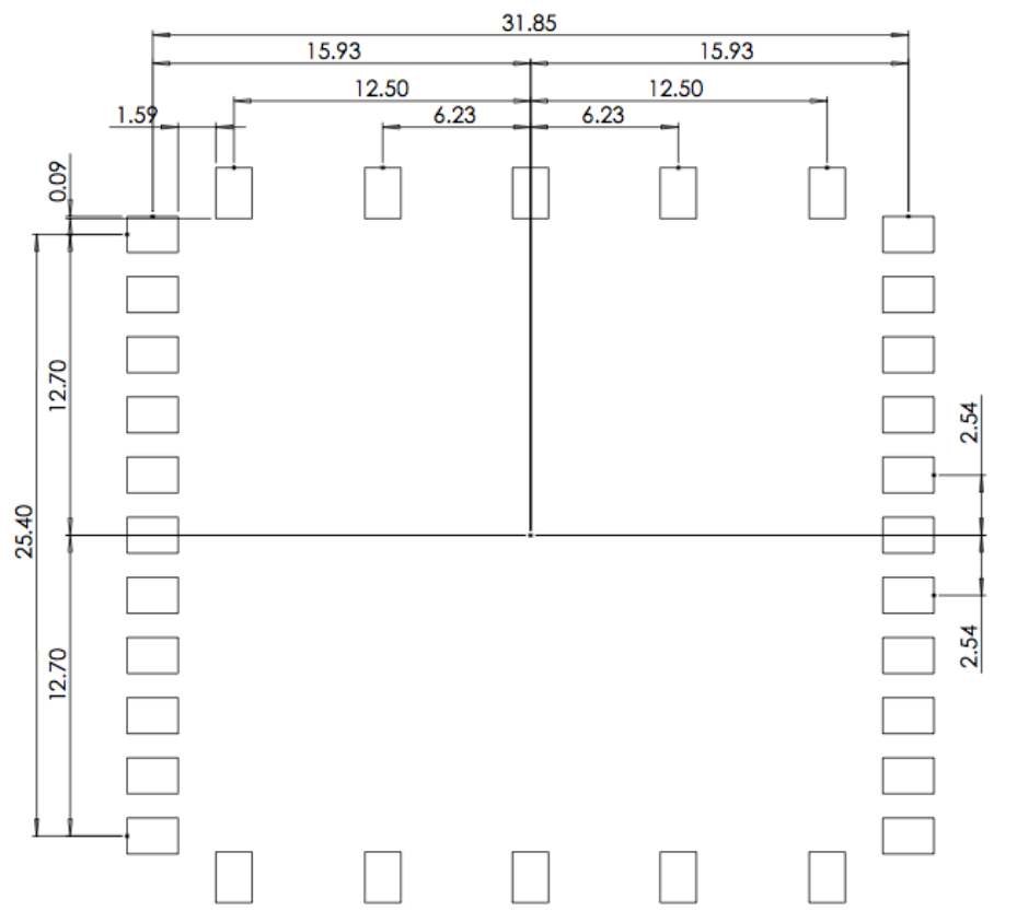
7.2 Package Dimensions
Package dimensions are shown in Figure 8-1 and Figure 8-2.
All dimensions are in millimeters.
Dimension tolerances (unless otherwise specified):
X = 1.0
X.X = 0.5
X.XX = 0.25
X.XXX = 0.125
Hole = 0.075
Angular: MACH 0.5
Bend: 1.0 Degree
18
Revision 1.1, Copyright © 2014, Impinj, Inc.
Table 8-1: RS500 Serial # Makeup
Digits
Meaning
XX
SKU code:
01 = GX
02 = EU
ZZ
Lot number
WW
Workweek produced
YY
Year produced
AAAA
Serial number within
the lot
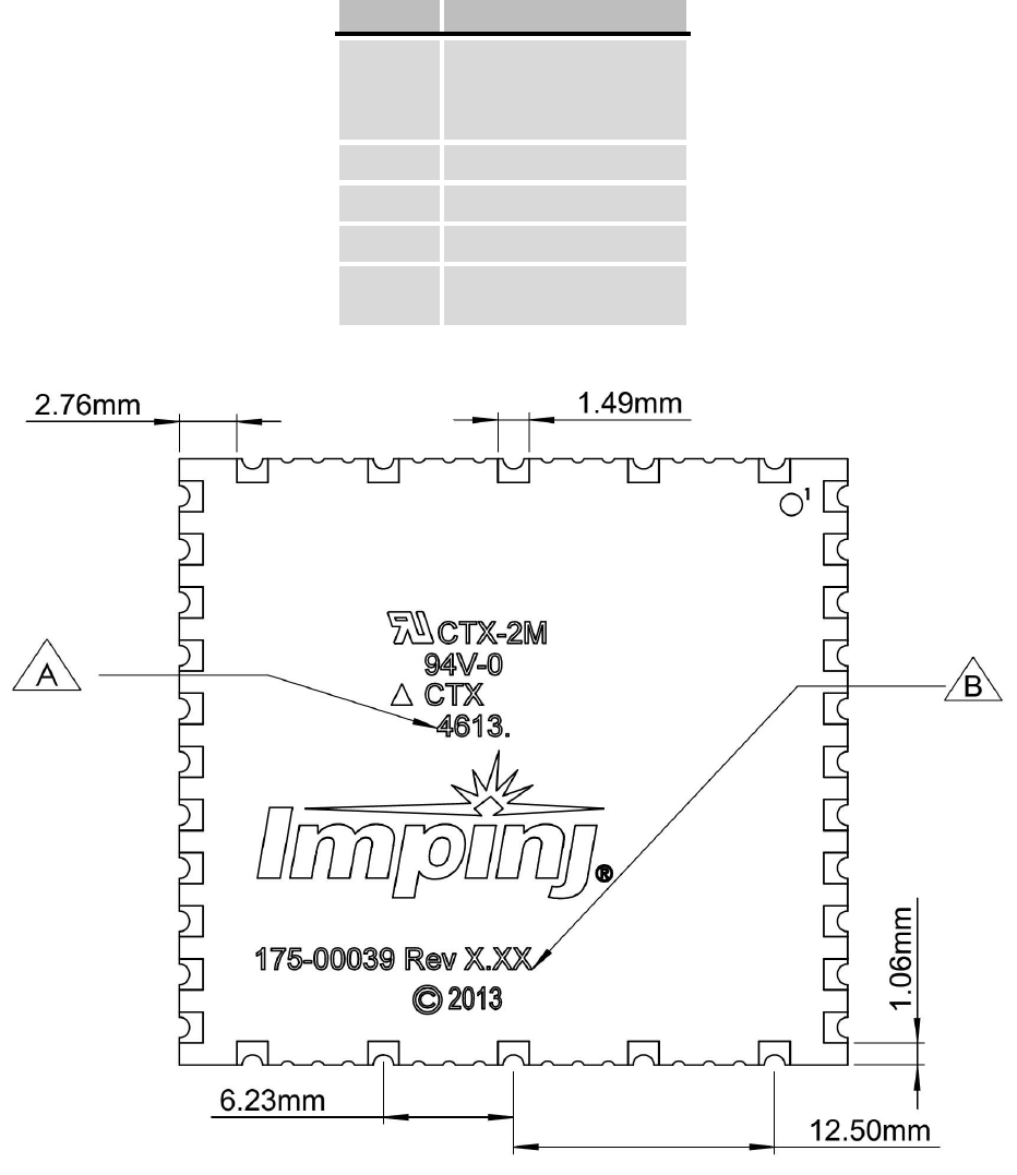
Figure 8-2: RS500 Pin Dimensions (viewed from underneath package)
Note. Callouts A and B show package markings that will vary depending on the
manufacturing lot of the RS500 unit.
20
Revision 1.1, Copyright © 2014, Impinj, Inc.
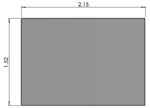
Figure 8-4: RS500 Recommended Etched Copper Footprint – Single Pad
22
Revision 1.1, Copyright © 2014, Impinj, Inc.
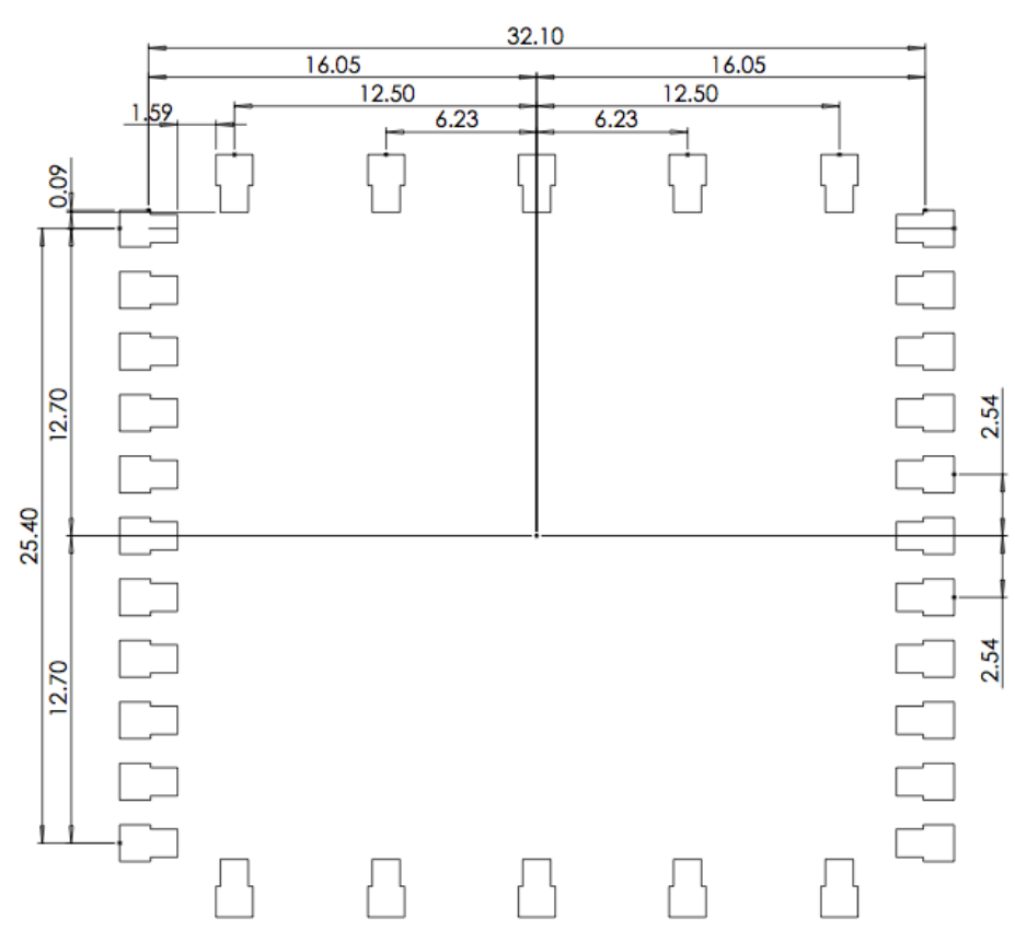
Figure 8-5: RS500 Recommended Pastemask Footprint – All Pads
Revision 1.1, Copyright © 2014, Impinj, Inc.
23
Figure 8-6: RS500 Recommended Pastemask Footprint – Single Pad
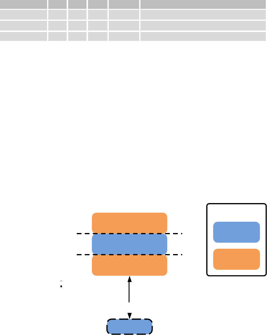
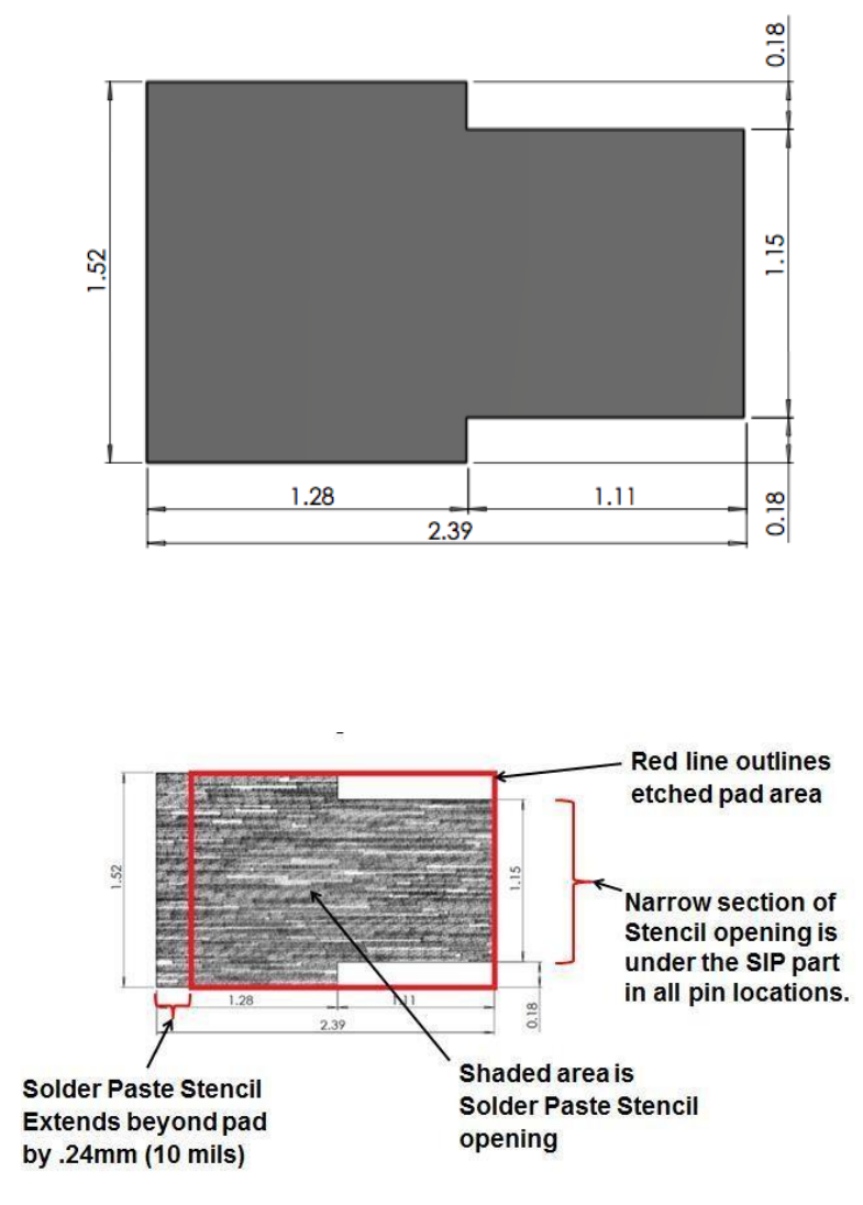
It is important to note that the optimal pad and stencil design results in a stencil aperture
that is of a different shape than and that overhangs the etched pad. This design delivers
the optimum amount of solder to the castellation of the SiP pad. Figure 8-7 depicts the
pad/solder relationship.
Figure 8-7: Recommended Solder Stencil Opening with Etched Pad for RS500
24
Revision 1.1, Copyright © 2014, Impinj, Inc.
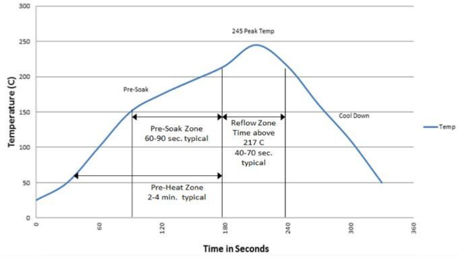
7.4 SMT Reflow Information
No-clean Type 3 Sn3Ag0.5Cu Solder Paste (Koki S3X58- M650) was used during
Impinj’s testing of the Indy RS500. The solder manufacturer’s recommended reflow
profile is shown in Figure 8-8.
Figure 8-8: Recommended Solder Reflow Profile for the Indy RS500

Revision 1.1, Copyright © 2014, Impinj, Inc.
25
8 Document Change Log
Table 9-1: Document Change Log
Version
Date
Description
1.0
Initial version
1.1
4/30/2014
Package drawings updated
Spec clarifications
Regulatory information moved to Hardware User’s Guide
Formatting updates
Change log added
9 Notices
Copyright © 2014, Impinj, Inc. All rights reserved.
Impinj gives no representation or warranty, express or implied, for accuracy or reliability
of information in this document. Impinj reserves the right to change its products and
services and this information at any time without notice.
EXCEPT AS PROVIDED IN IMPINJ’S TERMS AND CONDITIONS OF SALE (OR AS
OTHERWISE AGREED IN A VALID WRITTEN INDIVIDUAL AGREEMENT WITH
IMPINJ), IMPINJ ASSUMES NO LIABILITY WHATSOEVER AND IMPINJ DISCLAIMS
ANY EXPRESS OR IMPLIED WARRANTY, RELATED TO SALE AND/OR USE OF
IMPINJ PRODUCTS INCLUDING LIABILITY OR WARRANTIES RELATING TO
FITNESS FOR A PARTICULAR PURPOSE, MERCHANTABILITY, OR
INFRINGEMENT.
NO LICENSE, EXPRESS OR IMPLIED, BY ESTOPPEL OR OTHERWISE, TO ANY
PATENT, COPYRIGHT, MASK WORK RIGHT, OR OTHER INTELLECTUAL
PROPERTY RIGHT IS GRANTED BY THIS DOCUMENT.
Impinj assumes no liability for applications assistance or customer product design.
Customers should provide adequate design and operating safeguards to minimize risks.
Impinj products are not designed, warranted or authorized for use in any product or
application where a malfunction may reasonably be expected to cause personal injury
or death or property or environmental damage (“hazardous uses”) or for use in
automotive environments. Customers must indemnify Impinj against any damages
arising out of the use of Impinj products in any hazardous or automotive uses.
Indy is a trademark of Impinj, Inc. All other product or service names are trademarks of
their respective companies.
www.impinj.com
Federal Communication Commission Interference Statement
This device complies with Part 15 of the FCC Rules. Operation is subject to the following two
conditions: (1) This device may not cause harmful interference, and (2) this device must
accept any interference received, including interference that may cause undesired operation.
This equipment has been tested and found to comply with the limits for a Class B digital
device, pursuant to Part 15 of the FCC Rules. These limits are designed to provide reasonable
protection against harmful interference in a residential installation. This equipment generates,
uses and can radiate radio frequency energy and, if not installed and used in accordance with
the instructions, may cause harmful interference to radio communications. However, there is
no guarantee that interference will not occur in a particular installation. If this equipment does
cause harmful interference to radio or television reception, which can be determined by
turning the equipment off and on, the user is encouraged to try to correct the interference by
one of the following measures:
Reorient or relocate the receiving antenna.
Increase the separation between the equipment and receiver.
Connect the equipment into an outlet on a circuit different from that
to which the receiver is connected.
Consult the dealer or an experienced radio/TV technician for help.
FCC Caution:
Any changes or modifications not expressly approved by the party responsible for
compliance could void the user's authority to operate this equipment.
This transmitter must not be co-located or operating in conjunction with any other
antenna or transmitter.

Radiation Exposure Statement:
This equipment complies with FCC radiation exposure limits set forth for an uncontrolled
environment. This module can be used with T800 or similar platform with similar dimension,
antenna location and RF characteristic.
This device is intended only for OEM integrators under the following conditions:
1)
The antenna must be installed at the same location as tested in the certification filing, and
the maximum antenna gain allowed for use with this device is 4.41 dBi.
2)
The transmitter module may not be co-located with any other transmitter or antenna.
3)
For portable usage condition, this module has been SAR evaluated in T800 host with
compliance result and can be used with this specific host as described in the certification
filing. Other host or platform needs separate approval.
As long as 3 conditions above are met, further transmitter test will not be required.
However, the OEM integrator is still responsible for testing their end-product for any
additional compliance requirements required with this module installed
IMPORTANT NOTE: In the event that these conditions can not be met (for example certain
laptop configurations or co-location with another transmitter), then the FCC authorization is
no longer considered valid and the FCC ID can not be used on the final product. In these
circumstances, the OEM integrator will be responsible for re-evaluating the end product
(including the transmitter) and obtaining a separate FCC authorization.
End Product Labeling
The final end product must be labeled in a visible area with the following: “Contains FCC
ID: QYLRS500”. The grantee's FCC ID can be used only when all FCC compliance
requirements are met.
Manual Information To the End User
The OEM integrator has to be aware not to provide information to the end user regarding how
to install or remove this RF module in the user’s manual of the end product which integrates
this module. The end user manual shall include all required regulatory information/warning as
show in this manual.