Getac Technology V110RFID RFID MODULE User Manual 1
Getac Technology Corporation RFID MODULE 1
UserManual.wiki
>
Getac Technology
>
V110RFID User Manual
>
User Manual 1
Contents
1.
User Manual 1
2.
User Manual 2
User Manual 1
Navigation menu
Upload a User Manual
Namespaces
Wiki Guide
HTML
PDF
Info
Views
User Manual
Discussion / Help
Navigation
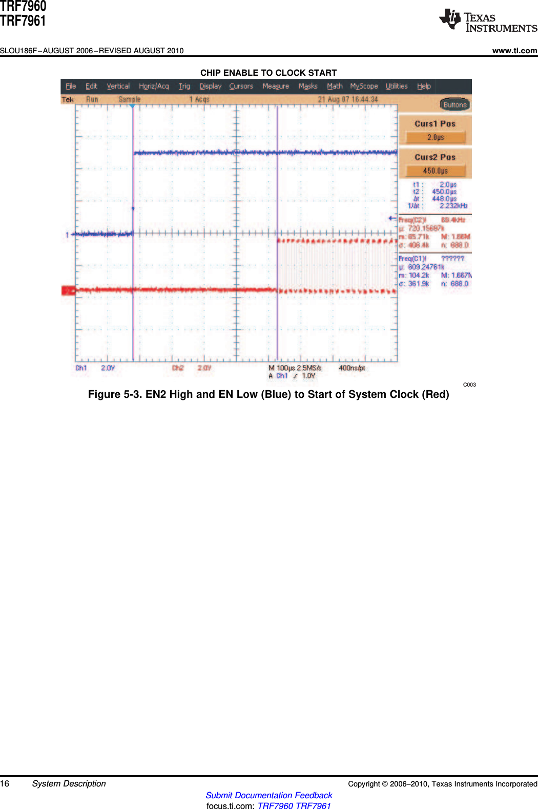
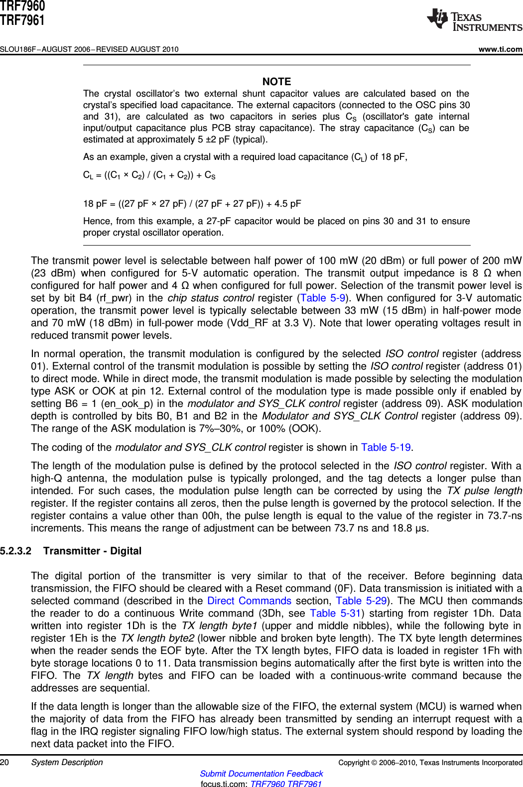
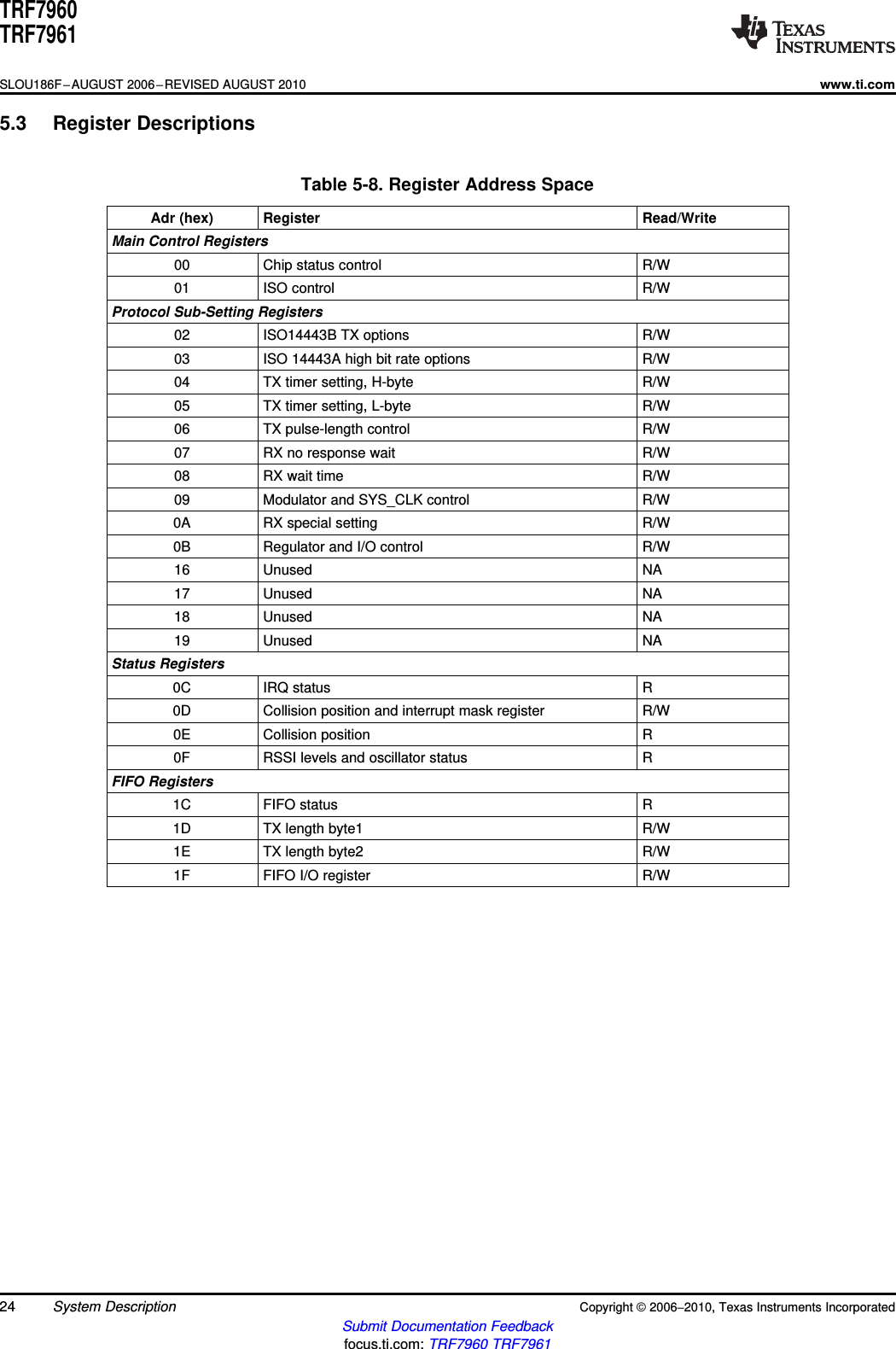
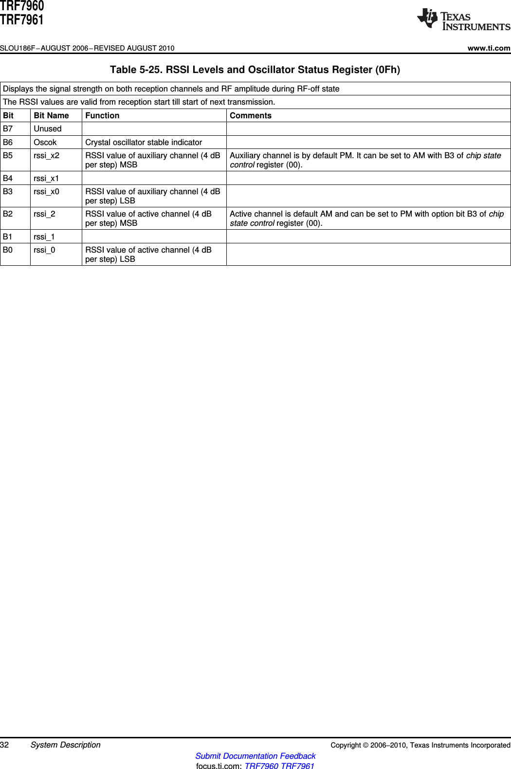
![C001C002TRF7960TRF7961www.ti.comSLOU186F–AUGUST 2006–REVISED AUGUST 20105.1.5 Timing DiagramsCHIP POWER UP TO CLOCK STARTFigure 5-1. Power Up [VIN (Blue) to Crystal Start (Red)]CHIP ENABLE TO CLOCK STARTFigure 5-2. EN2 Low and EN High (Blue) to Start of System Clock (Red)Copyright ©2006–2010, Texas Instruments Incorporated System Description 15Submit Documentation Feedbackfocus.ti.com: TRF7960 TRF7961](https://usermanual.wiki/Getac-Technology/V110RFID.User-Manual-1/User-Guide-2121324-Page-15.png)
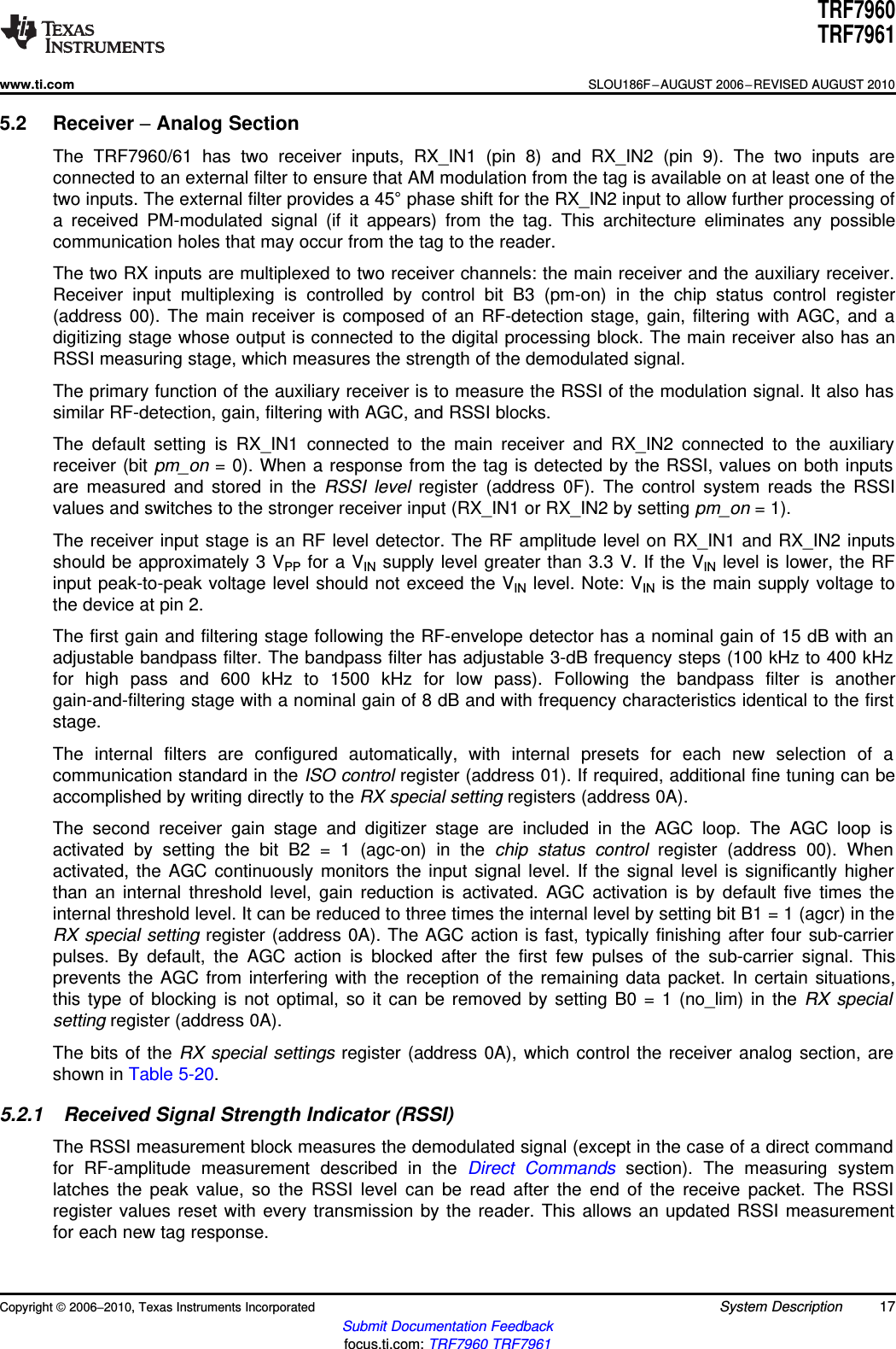
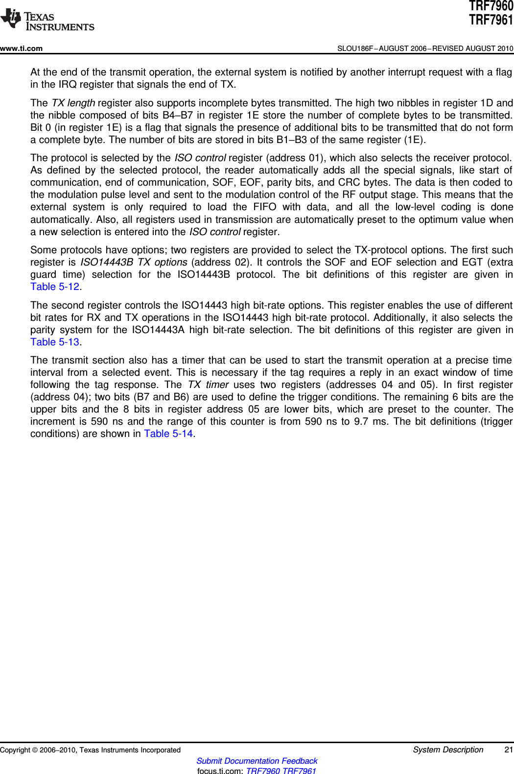
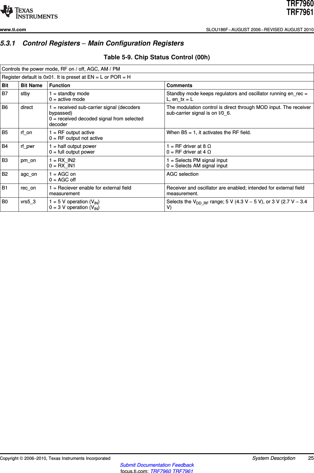
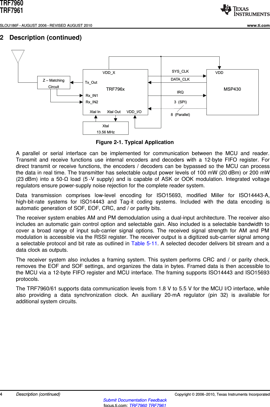
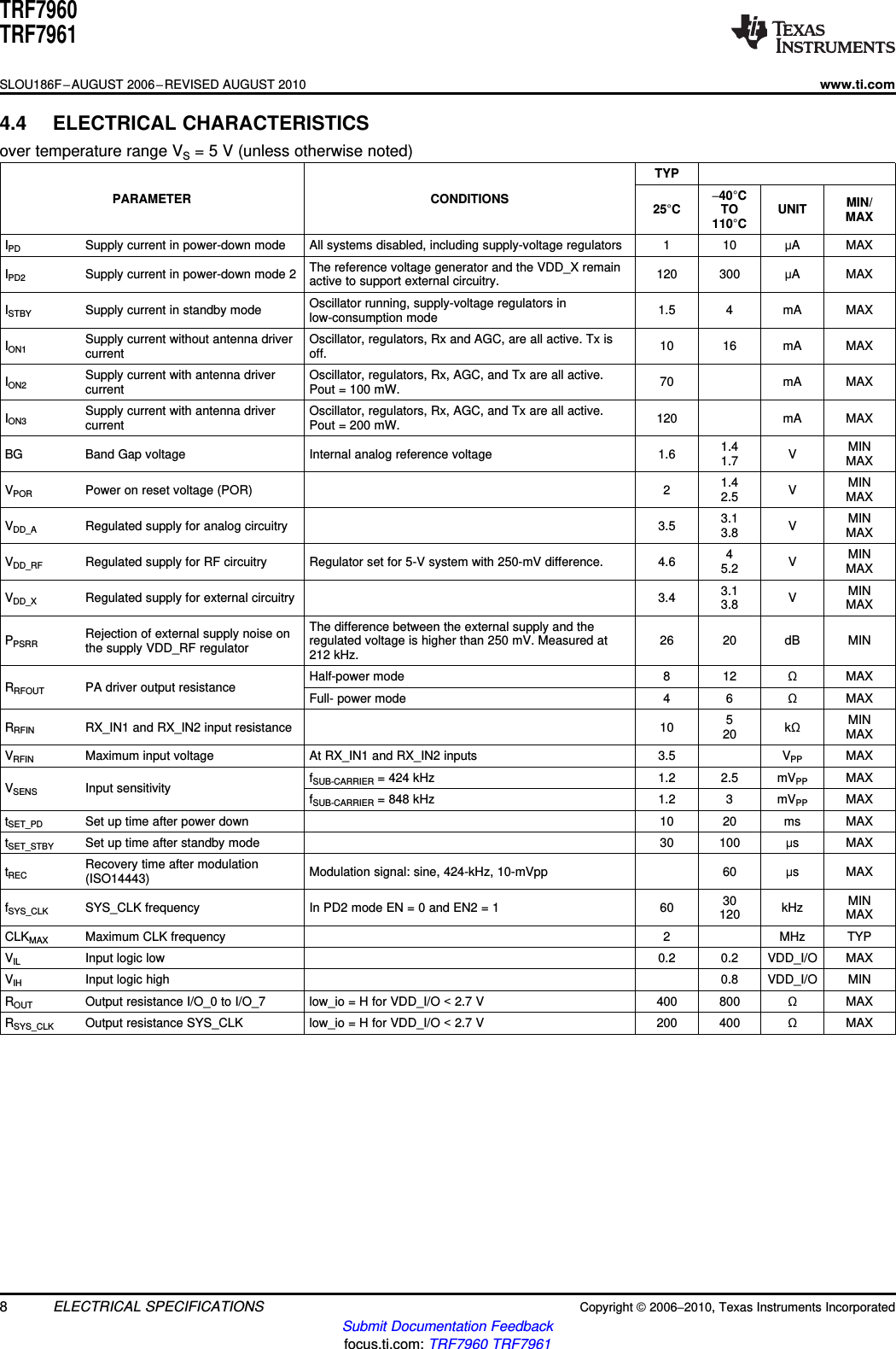
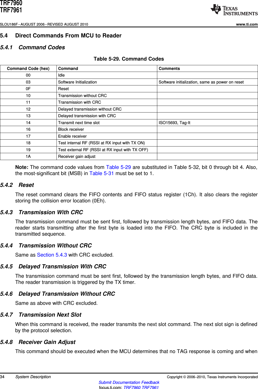
![TRF7960TRF7961www.ti.comSLOU186F–AUGUST 2006–REVISED AUGUST 20105.3.4 FIFO Control RegistersTable 5-26. FIFO Status (1Ch)Low nibbles of complete bytes to be transferred through FIFO; Information about a broken byte and number of bits to be transferred from itBit Bit Name Function CommentsB7 RFU Set to LOW Reserved for future use (RFU)B6 Fhil FIFO level HIGH Indicates that 9 bytes are already in the FIFO (for RX)B5 Flol FIFO level LOW Indicates that only 3 bytes are in the FIFO (for TX)B4 Fove FIFO overflow error Too much data was written to the FIFOB3 Fb3 FIFO bytes fb[3] Bits B0:B3 indicate how many bytes that are loaded in FIFO were not readout yet (displays N –1 number of bytes). If 8 bytes are in the FIFO, thisnumber is 7.B2 Fb2 FIFO bytes fb[2]B1 Fb1 FIFO bytes fb[1]B0 Fb0 FIFO bytes fb[0]Table 5-27. TX Length Byte1 (1Dh)High 2 nibbles of complete bytes to be transferred through FIFORegister default is set to 0x00 at POR and EN=0. It is also automatically reset at TX EOFBit Bit Name Function CommentsB7 Txl11 Number of complete byte bn[11] High nibble of complete bytes to be transmittedB6 Txl10 Number of complete byte bn[10]B5 Txl9 Number of complete byte bn[9]B4 Txl8 Number of complete byte bn[8]B3 Txl7 Number of complete byte bn[7] Middle nibble of complete bytes to be transmittedB2 Txl6 Number of complete byte bn[6]B1 Txl5 Number of complete byte bn[5]B0 Txl4 Number of complete byte bn[4]Table 5-28. TX Length Byte2 (1Eh)Low nibbles of complete bytes to be transferred through FIFO; Information about a broken byte and number of bits to be transferred from itRegister default is set to 0x00 at POR and EN=0. It is also automatically reset at TX EOFBit Bit Name Function CommentsB7 Txl3 Number of complete byte bn[3] Low nibble of complete bytes to be transmittedB6 Txl2 Number of complete byte bn[2]B5 Txl1 Number of complete byte bn[1]B4 Txl0 Number of complete byte bn[0]B3 Bb2 Broken byte number of bits bb[2] Number of bits in the last broken byte to be transmitted.B2 Bb1 Broken byte number of bits bb[1] It is taken into account only when broken byte flag is set.B1 Bb0 Broken byte number of bits bb[0]B0 Bbf Broken byte flag If 1, indicates that last byte is not complete 8 bits wide.Copyright ©2006–2010, Texas Instruments Incorporated System Description 33Submit Documentation Feedbackfocus.ti.com: TRF7960 TRF7961](https://usermanual.wiki/Getac-Technology/V110RFID.User-Manual-1/User-Guide-2121324-Page-33.png)
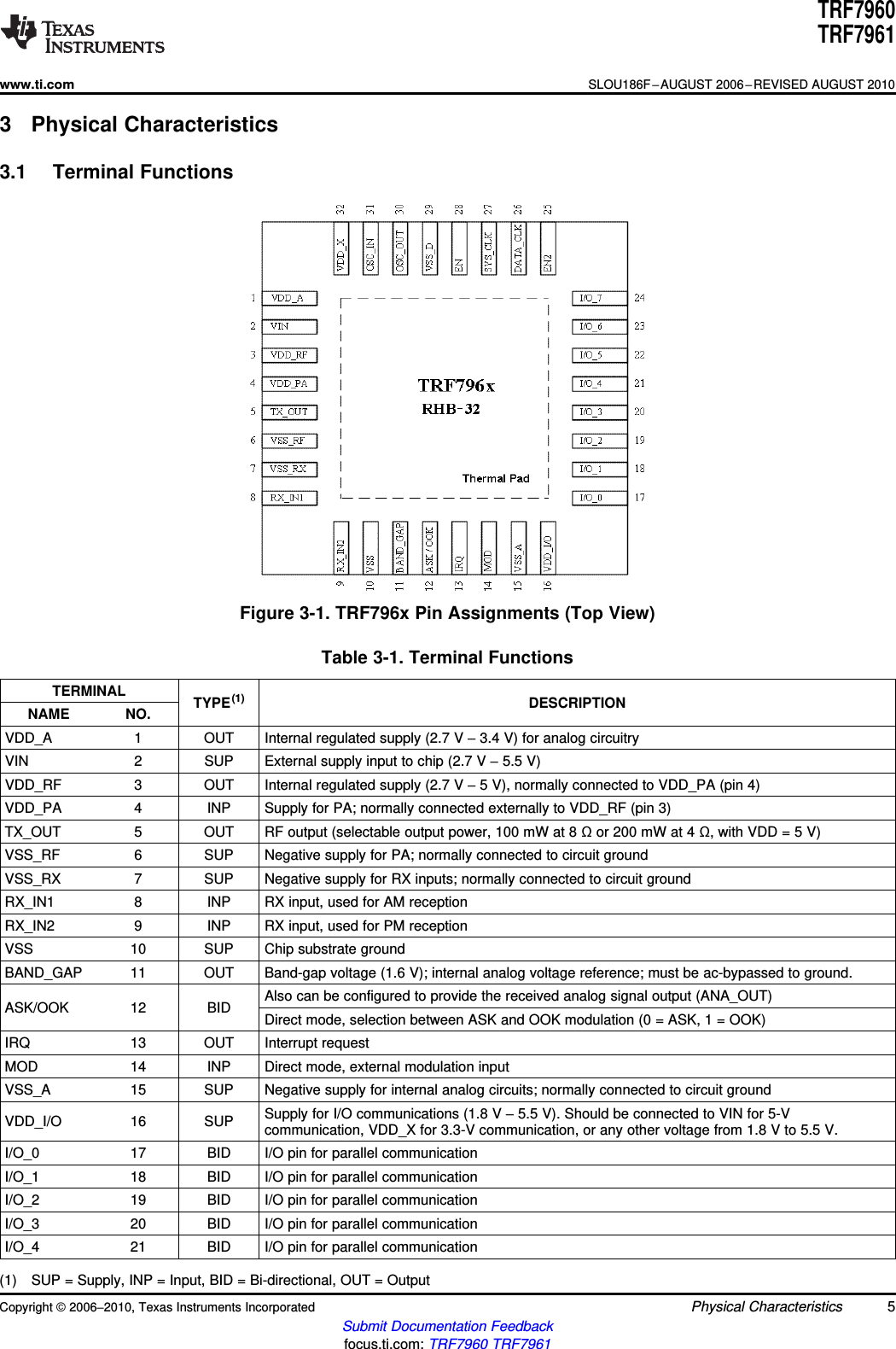
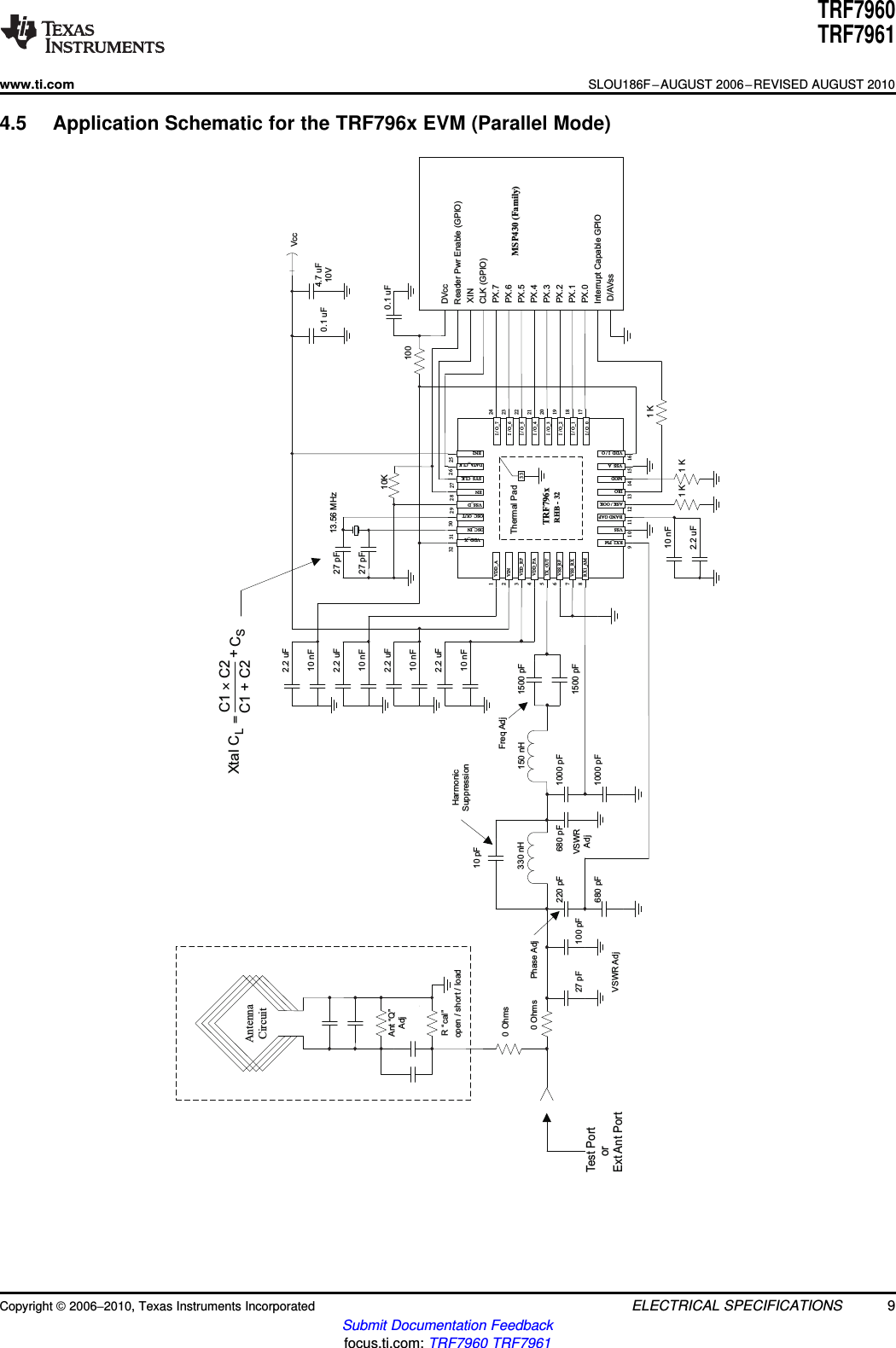
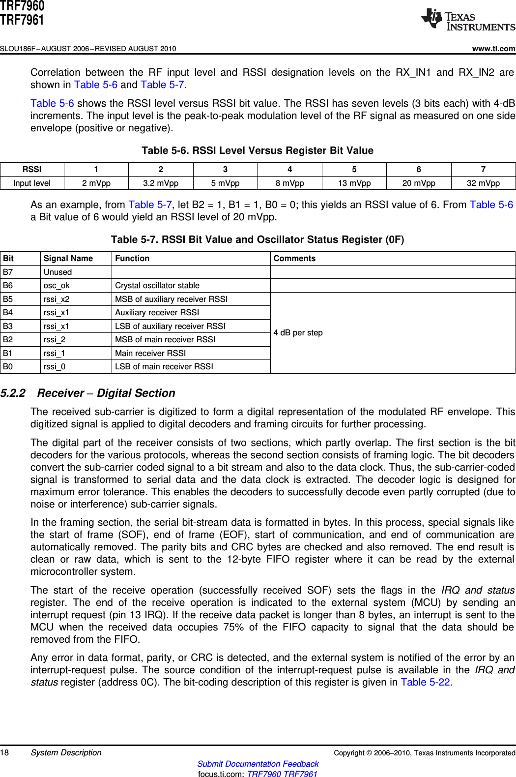
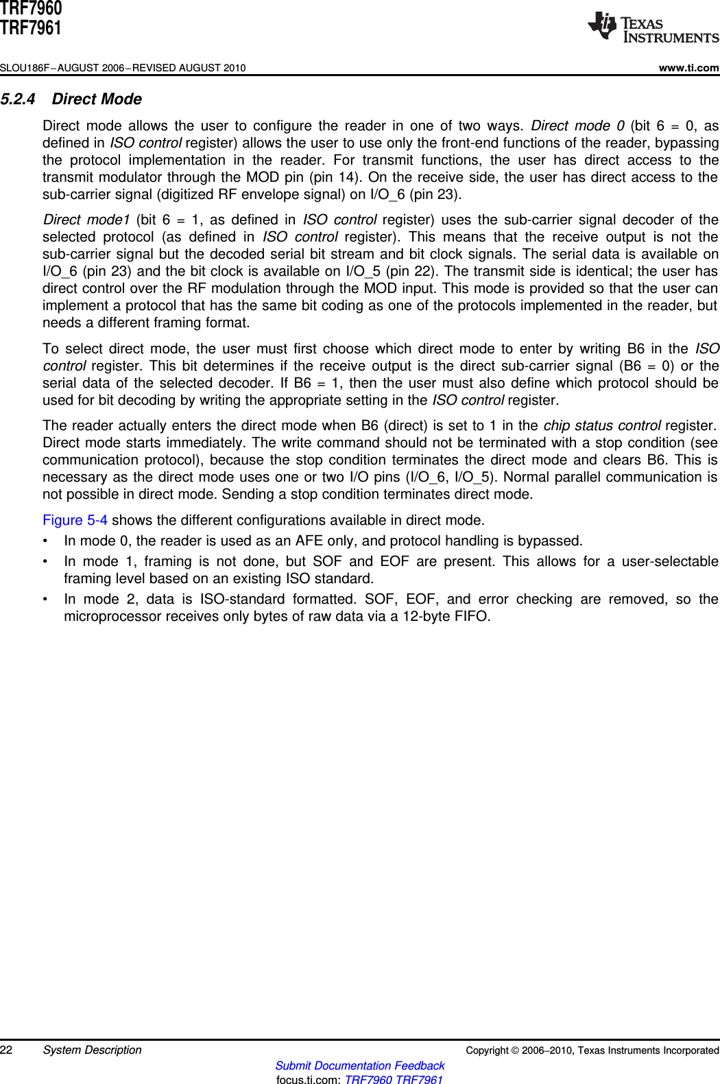
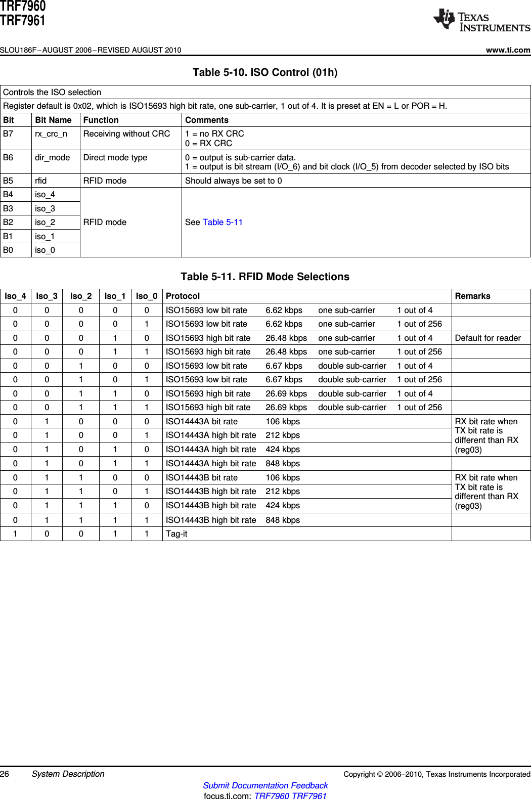
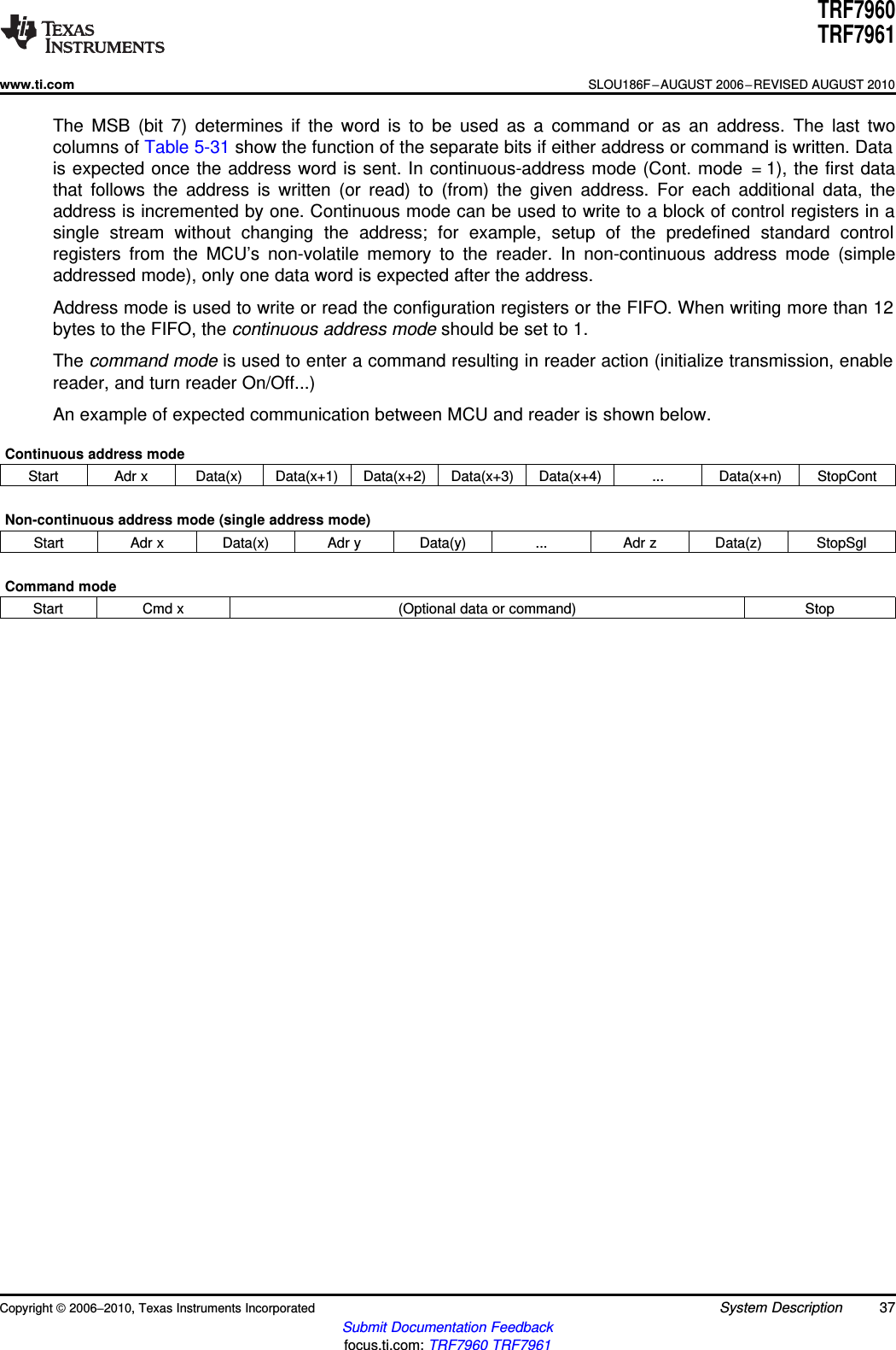
![TRF7960TRF7961www.ti.comSLOU186F–AUGUST 2006–REVISED AUGUST 2010the RF and receivers are switched ON. When this command is received, the reader observes the digitizedreceiver output. If more than two edges are observed in 100 μs, the window comparator voltage isincreased. The procedure is repeated until the number of edges (changes of logical state) of the digitizedreception signal is less than 2 (in 100 μs). The command can reduce the input sensitivity in 5-dBincrements up to 15 dB. This command ensures better operation in a noisy environment.The gain setting is reset to maximum gain at EN = 0, POR = 1.5.4.9 Test External RF (RSSI at RX input with TX OFF)This command can be used in active mode when the RF receiver is switched ON, and the RF output isswitched OFF (bit B1=1 in the chip status register, rec-on. See Table 5-9). The level of the RF signalreceived on the antenna is measured and displayed in the RSSI levels register. The relation between the3-bit code and the external RF field strength [A/m] must be determined by calculation or by experimentsfor each antenna design. The antenna Q and connection to the RF input influence the result. The nominalrelation between the RF peak-to-peak voltage at the receiver inputs and its corresponding RSSI level ispresented as follows.Receiver Input [mVPP] 40 60 80 100 140 180 300RSSI level 1 2 3 4 5 6 7If the direct command test RF internal or test RF external is used immediately after activation, it should bepreceded with a command enable RX to activate the RX section. For proper execution of the test RFcommands, the RX section must be enabled. This happens automatically when a data exchange betweenthe reader and the tag is done, or by sending a direct command enable RX.5.4.10 Test Internal RF (RSSI at RX input with TX ON)This command measures the level of the RF carrier at the receive inputs. Its operating range is between300 mVp and 2.1 Vp with a step size of 300 mV. The two values are displayed in the RSSI levels register.The command is intended for diagnostic purposes to set the correct RX_IN levels. The optimum RX_INinput level is approximately 1.6 Vp, or an RSSI level of 5 or 6. The nominal relationship between the inputRF peak level and the RSSI code is presented as follows.Receiver Input [mVPp] 300 600 900 1200 1500 1800 2100RSSI Level 1 2 3 4 5 6 75.4.11 Block ReceiverThe block receiver command puts the digital part of receiver (bit decoder and framer) in reset mode. Thisis useful in an extremely noisy environment, where the noise level could otherwise cause a constantswitching of the sub-carrier input of the digital part of the receiver. The receiver (if not in reset) would try tocatch a SOF signal, and if the noise pattern matched the SOF pattern, an interrupt would be generated,falsely signaling the start of an RX operation. A constant flow of interrupt requests can be a problem forthe external system (MCU), so the external system can stop this by putting the receive decoders in resetmode. The reset mode can be terminated in two ways. The external system can send the enable receivercommand. The reset mode is also automatically terminated at the end of a TX operation. The receiver canstay in reset after end of TX if the RX wait time register (address 08) is set. In this case, the receiver isenabled at the end of the wait time following the transmit operation.5.4.12 Enable ReceiverThis command clears the reset mode in the digital part of the receiver if the reset mode was entered bythe block receiver command.Copyright ©2006–2010, Texas Instruments Incorporated System Description 35Submit Documentation Feedbackfocus.ti.com: TRF7960 TRF7961](https://usermanual.wiki/Getac-Technology/V110RFID.User-Manual-1/User-Guide-2121324-Page-35.png)
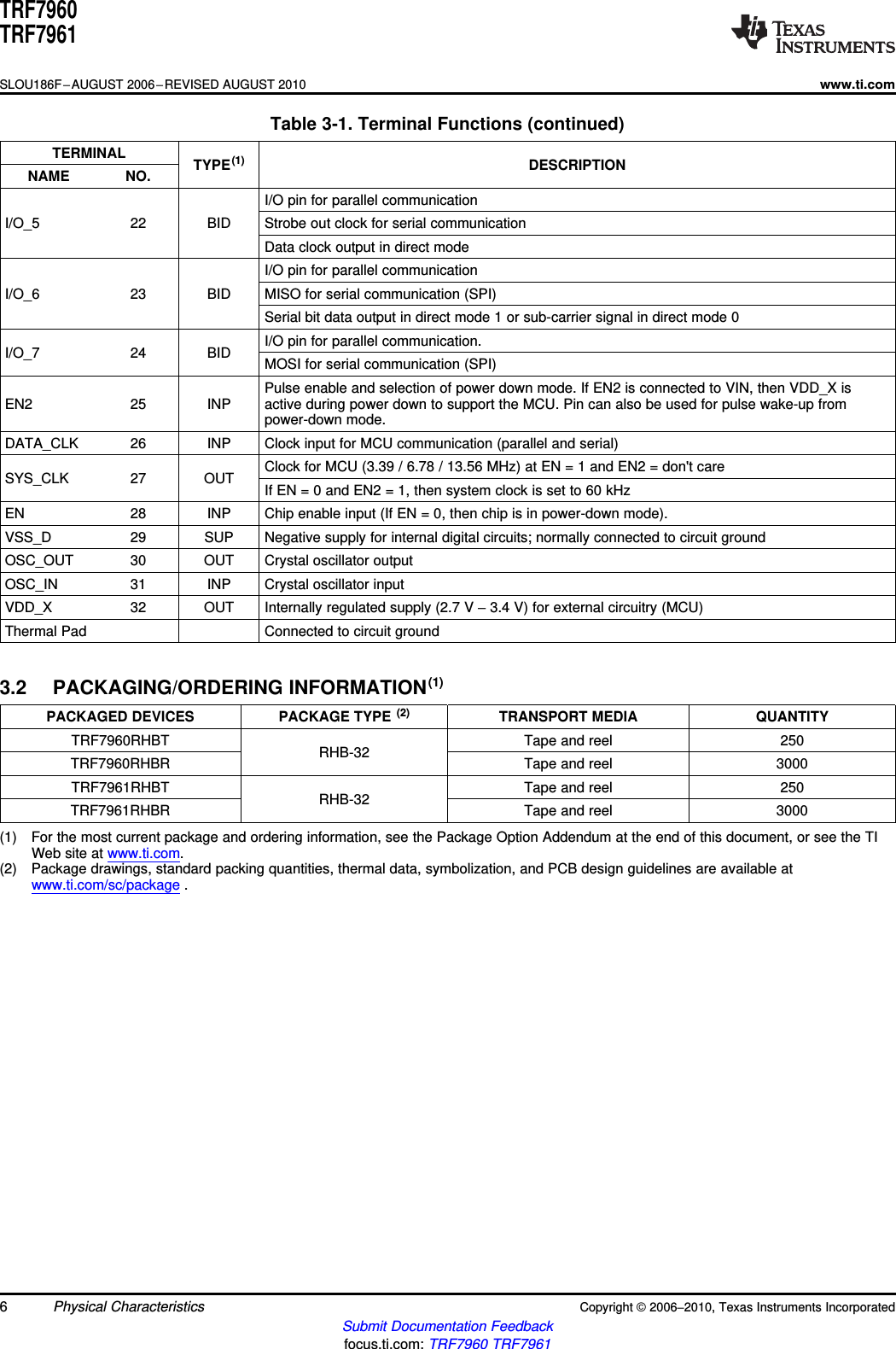
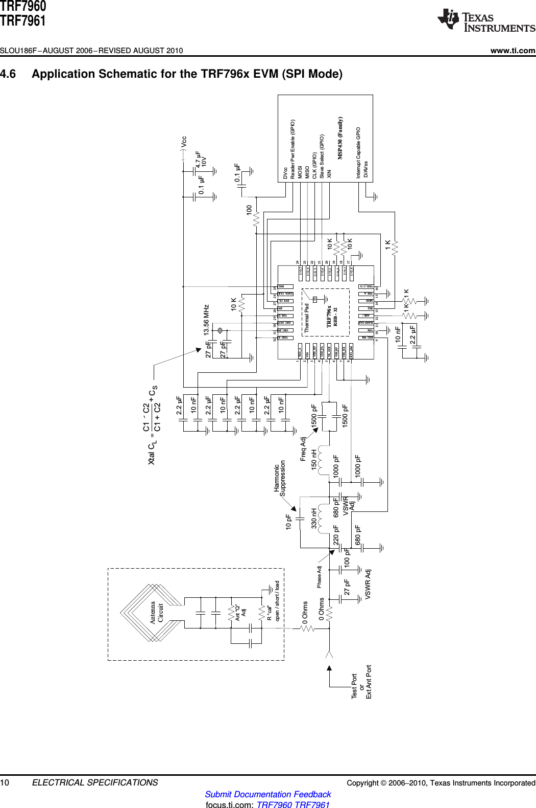
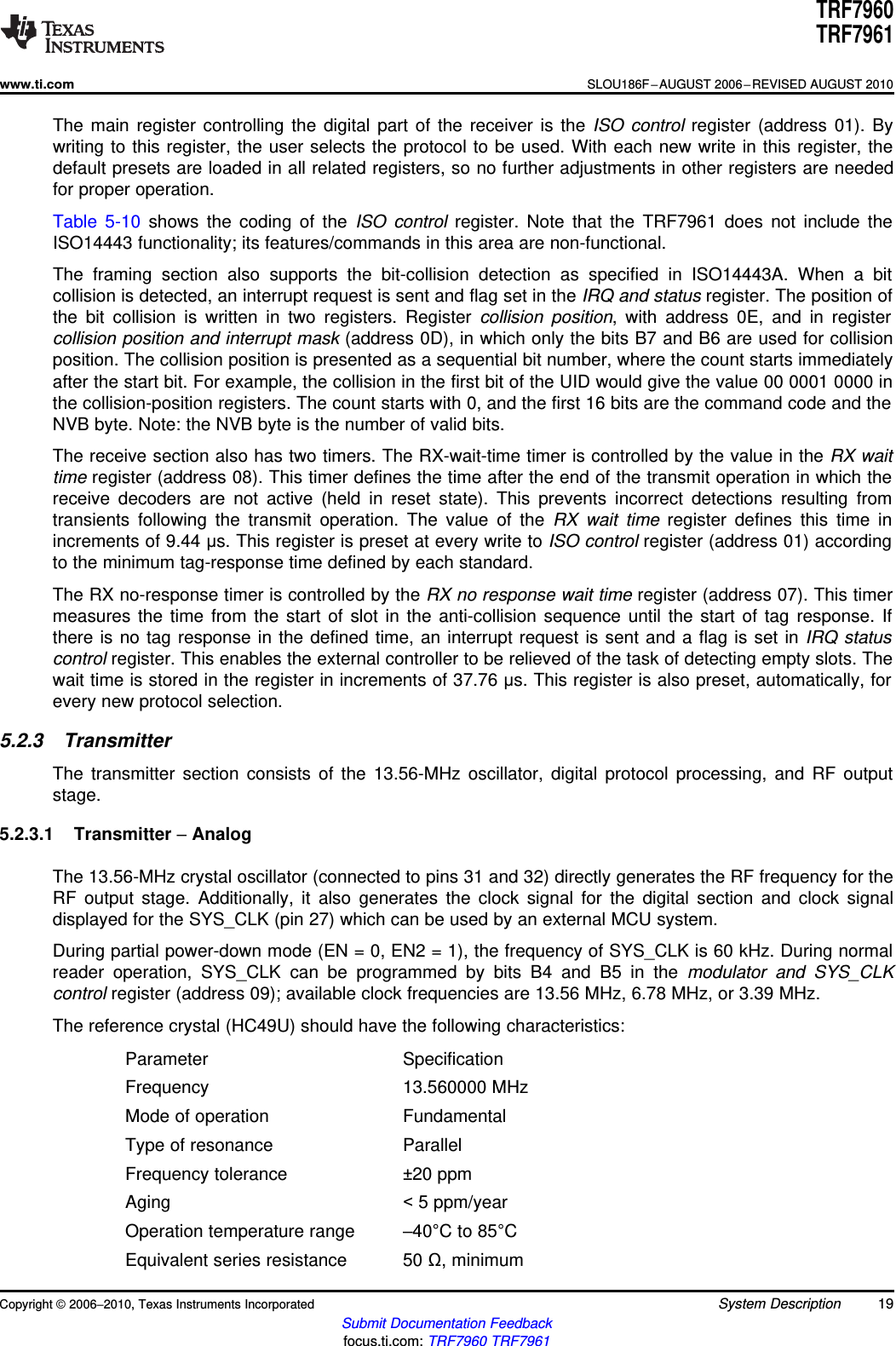
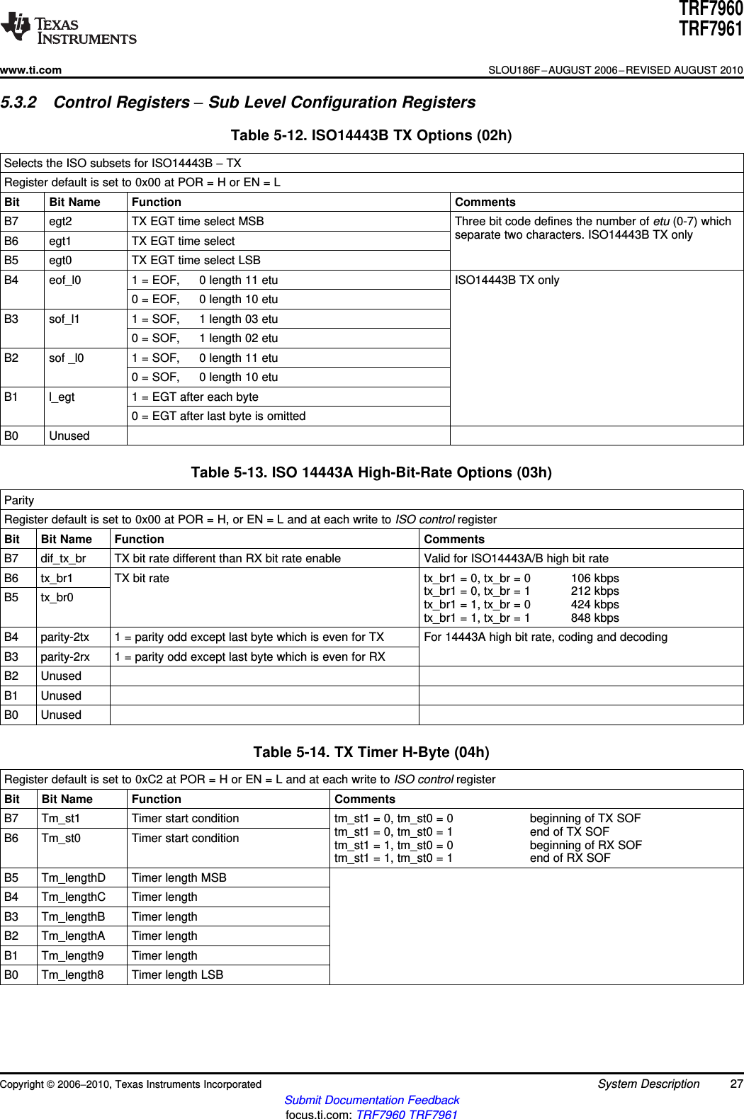
![TRF7960TRF7961SLOU186F–AUGUST 2006–REVISED AUGUST 2010www.ti.com5.5 Reader Communication Interface5.5.1 IntroductionThe communication interface to the reader can be configured in two ways: a parallel 8-pin interface and aData_Clk or a serial peripheral interface (SPI).These modes are mutually exclusive; only one mode can be used at a time in the application.When the SPI interface is selected, the unused I/O_2, I/O_1, and I/O_0 pins must be hard-wired accordingto Table 5-30. At power up, the reader samples the status of these three pins. If they are not the same (allHigh or all Low) it enters one of the possible SPI modes.The reader always behaves as the slave while the microcontroller (MCU) behaves as the master device.The MCU initiates all communications with the reader and is also used to communicate with the higherlevels (application layer). The reader has an IRQ pin to prompt the MCU for attention if the reader detectsa response from the proximity/vicinity integrated circuit card (PICC/VICC).Communication is initialized by a start condition, which is expected to be followed by anAddress/Command word (Adr/Cmd). The Adr/Cmd word is 8 bits long, and its format is shown inTable 5-31.Table 5-30. Pin Assignment in Parallel and Serial Interface Connection or Direct ModePin Parallel Parallel-Direct SPI with SS SPI without SSDATA_ DATA_CLK DATA_CLK DATA_CLK from master DATA_CLK from masterCLKI/O_7 A/D[7] MOSI(1) = data-in (reader-in) MOSI(1) = data-in(reader-in)I/O_6 A/D[6] Direct mode, data out (sub-carrier or bit stream) MISO(2) = data-out (MCU-out) MISO(2) = data-out(MCU-out)I/O_5(3) A/D[5] Direct mode, strobe –bit clock out See Note 3 See Note 3I/O_4 A/D[4] SS –slave select(4) —I/O_3 A/D[3] — — —I/O_2 A/D[2] —at VDD at VDDI/O_1 A/D[1] —at VDD at VSSI/O_0 A/D[0] —at VSS at VSSIRQ IRQ interrupt IRQ interrupt IRQ interrupt IRQ interrupt(1) MOSI –master out, slave in(2) MISO –master in, slave out(3) IO_5 pin is used only for information when data is put out of the chip (for example, reading 1 byte from the chip). It is necessary first towrite in the address of the register (8 clocks) and then to generate another 8 clocks for reading out the data. The IO_5 pin goes high inthis second 8 clocks. But for normal SPI operation this pin IO_5 is not used.(4) Slave-select pin active-lowTable 5-31. Address/Command Word Bit DistributionBit Description Bit Function Address CommandBit 7 Command control bit 0 = address, 1 = command 0 1Bit 6 Read/Write 1 = read, 0 = write R/W 0Bit 5 Continuous address mode 1 = Cont. mode R/W 0Bit 4 Address/Command bit 4 Adr 4 Cmd 4Bit 3 Address/Command bit 3 Adr 3 Cmd 3Bit 2 Address/Command bit 2 Adr 2 Cmd 2Bit 1 Address/Command bit 1 Adr 1 Cmd 1Bit 0 Address/Command bit 0 Adr 0 Cmd 036 System Description Copyright ©2006–2010, Texas Instruments IncorporatedSubmit Documentation Feedbackfocus.ti.com: TRF7960 TRF7961](https://usermanual.wiki/Getac-Technology/V110RFID.User-Manual-1/User-Guide-2121324-Page-36.png)
![a1[7] d1[7] a2[7] d2[7] aN[7] dN[7]StartConditionStopSmplConditionCLKI/O_[7]I/O_[6:0]a1[6:0] a2[6:0]d1[6:0] d2[6:0] aN[6:0] dN[6:0]50nsa0[7] d0[7]StartConditionCLKI/O_[7]I/O_[6:0] a0[6:0] d0[6:0]xx d1[6:0] d2[6:0]d2[7]dN[6:0]d3[6:0]dN[7]xxStopContContinuousModed1[7] d3[7]50nsTRF7960TRF7961SLOU186F–AUGUST 2006–REVISED AUGUST 2010www.ti.com5.6 Parallel Interface CommunicationIn parallel mode, the start condition is generated on the rising edge of the I/O_7 pin while the CLK is high.This is used to reset the interface logic. Figure 5-5 shows the sequence of the data, with an 8-bit addressword first, followed by data.Communication is ended by:•the StopSmpl condition, where the falling edge on the I/O_7 pin is expected while CLK is high•the StopCont condition, where the I/O_7 pin must have a successive rising and falling edge while CLKis low in order to reset the parallel interface and be ready for the new communication sequenceThe StopSmpl condition is also used to terminate the direct mode.Figure 5-5. Parallel Interface Communication With Simple Stop Condition StopSmplFigure 5-6. Parallel Interface Communication With Continuous Stop Condition StopCont38 System Description Copyright ©2006–2010, Texas Instruments IncorporatedSubmit Documentation Feedbackfocus.ti.com: TRF7960 TRF7961](https://usermanual.wiki/Getac-Technology/V110RFID.User-Manual-1/User-Guide-2121324-Page-38.png)
![StartConditionCLKI/O_[7]I/O_[6:0]a0[6:0]d0[6:0]xxd1[6:0]d2[6:0]dN[6:0]d3[6:0]xxStopContValidOuputDataa0[7]d0[7]d2[7]dN[7]d1[7]d3[7]InternalOEOutputData50nsTRF7960TRF7961www.ti.comSLOU186F–AUGUST 2006–REVISED AUGUST 20105.6.1 ReceiveAt the start of a receive operation (when SOF is successfully detected), B6 is set in the IRQ statusregister. An interrupt request is sent to the MCU at the end of the receive operation if the receive datastring was shorter than or equal to 8 bytes. The MCU receives the interrupt request, then checks todetermine the reason for the interrupt by reading the IRQ status register (address 0Ch), after which theMCU reads the data from the FIFO.If the received packet is longer than 8 bytes, the interrupt is sent before the end of the receive operationwhen the ninth byte is loaded into the FIFO (75% full). The MCU should again read the content of the IRQstatus register to determine the cause of the interrupt request. If the FIFO is 75% full (as marked with flagB5 in IRQ status register and by reading the FIFO status register), the MCU should respond by readingthe data from FIFO to make room for new incoming receive data. When the receive operation is finished,the interrupt is sent and the MCU must check how many words are still present in the FIFO before itfinishes reading.If the reader detects a receive error, the corresponding error flag is set (framing error, CRC error) in theIRQ status register, which indicates that the MCU reception was completed incorrectly.5.6.2 TransmitBefore beginning data transmission, the FIFO should be cleared with a reset command (0F). Datatransmission is initiated with a selected command (described in the Direct Commands section,Table 5-29). The MCU then commands the reader to do a continuous write command (3Dh, seeTable 5-31) starting from register 1Dh. Data written into register 1Dh is the TX length byte1 (upper andmiddle nibbles), while the following byte in register 1Eh is the TX length byte 2 (lower nibble and brokenbyte length). Note that the TX byte length determines when the reader sends the EOF byte. After the TXlength bytes are written, FIFO data is loaded in register 1Fh with byte storage locations 0 to 11. Datatransmission begins automatically after the first byte is written into the FIFO. The loading of TX lengthbytes and the FIFO can be done with a continuous-write command, as the addresses are sequential.At the start of transmission, the flag B7 (Irq_tx) is set in the IRQ status register. If the transmit data isshorter than or equal to 4 bytes, the interrupt is sent only at the end of the transmit operation. If thenumber of bytes to be transmitted is higher or equal to 5, then the interrupt is generated. This occurs alsowhen the number of bytes in the FIFO reaches 3. The MCU should check the IRQ status register andFIFO status register and then load additional data to the FIFO, if needed. At the end of the transmitoperation, an interrupt is sent to inform the MCU that the task is complete.Figure 5-7. Data Output Only When CLK Is HighCopyright ©2006–2010, Texas Instruments Incorporated System Description 39Submit Documentation Feedbackfocus.ti.com: TRF7960 TRF7961](https://usermanual.wiki/Getac-Technology/V110RFID.User-Manual-1/User-Guide-2121324-Page-39.png)