Green Point Jabil Design Services Branch TGPBA0010260 ZigBee Interface Module User Manual Ember Module Product Manual update by BVADT v2
Taiwan Green Point Enterprises Co., Ltd. Jabil Des ZigBee Interface Module Ember Module Product Manual update by BVADT v2
User Manual
Product Manual
JABIL Technology Services Design Services
Low Power ZigBee Module
(Ember)
TABLE OF AUTHORISATION
Name Role Organisation Signature
Thomas Chang PM PMO Thomas
Frank Liu Desing Manager R&D Frank
DOCUMENT HISTORY
Date Version
Status Author Change
12/20/1
0 1.0 Draft Yao-Ling
Cheng Initial Release
TABLE OF CONTENTS
1
INTRODUCTION..........................................................................................................................................3
1.1
P
URPOSE
..............................................................................................................................................3
1.2
S
COPE
...................................................................................................................................................3
1.3
I
NTENDED
A
UDIENCE
............................................................................................................................3
1.4
D
EFINITIONS AND ABBREVIATIONS
........................................................................................................3
2
OVERVIEW..................................................................................................................................................4
3
CONSTRAINTS, ASSUMPTIONS, AND DEPENDENCIES..................................................................5
4
FEATURES...................................................................................................................................................6
5
BLOCK DIAGRAM AND PORT FUNCTION ..........................................................................................7
5.1
UART
P
ORT
.........................................................................................................................................7
5.2
P
ROGRAMMING AND
D
EBUG
P
ORT
.......................................................................................................7
5.3
GPIO
P
ORT
..........................................................................................................................................7
6
DETAIL SPECIFICATIONS......................................................................................................................8
6.1
P
IN
A
SSIGNMENT
...................................................................................................................................8
6.1.1
LPZigBee Module ..........................................................................................................................8
6.2
E
LECTRICAL
S
PECIFICATION
................................................................................................................10
6.2.1
DC power supply range ..............................................................................................................10
6.2.2
System dBm max & min (maximum and minimum TX output at PCB antenna) and
System current & power drawn................................................................................................................10
6.2.3
System current & power drawn of TX@20dBm and RX........................................................10
6.2.4
System Current and Power consumption during idle and deep sleep mode...................................10
6.2.5
System RX Sensitivity (dBm)...........................................................................................................11

1 INTRODUCTION
1.1 P
URPOSE
The purpose of this document is to provide the product manual and Design
Specifications for low power ZigBee
(LPZigBee)
module.
1.2 S
COPE
The scope of this document is to produce the detail Design of LPZigBee module.
1.3 I
NTENDED
A
UDIENCE
This document is intended primarily for the EE Hardware Design.
1.4 D
EFINITIONS AND ABBREVIATIONS
Term Meaning
ADC Analog to Digital Converter
GPIO General Purpose Input/Output
I
2
C Inter Integrated Circuit
JTAG Joint Test Action Group
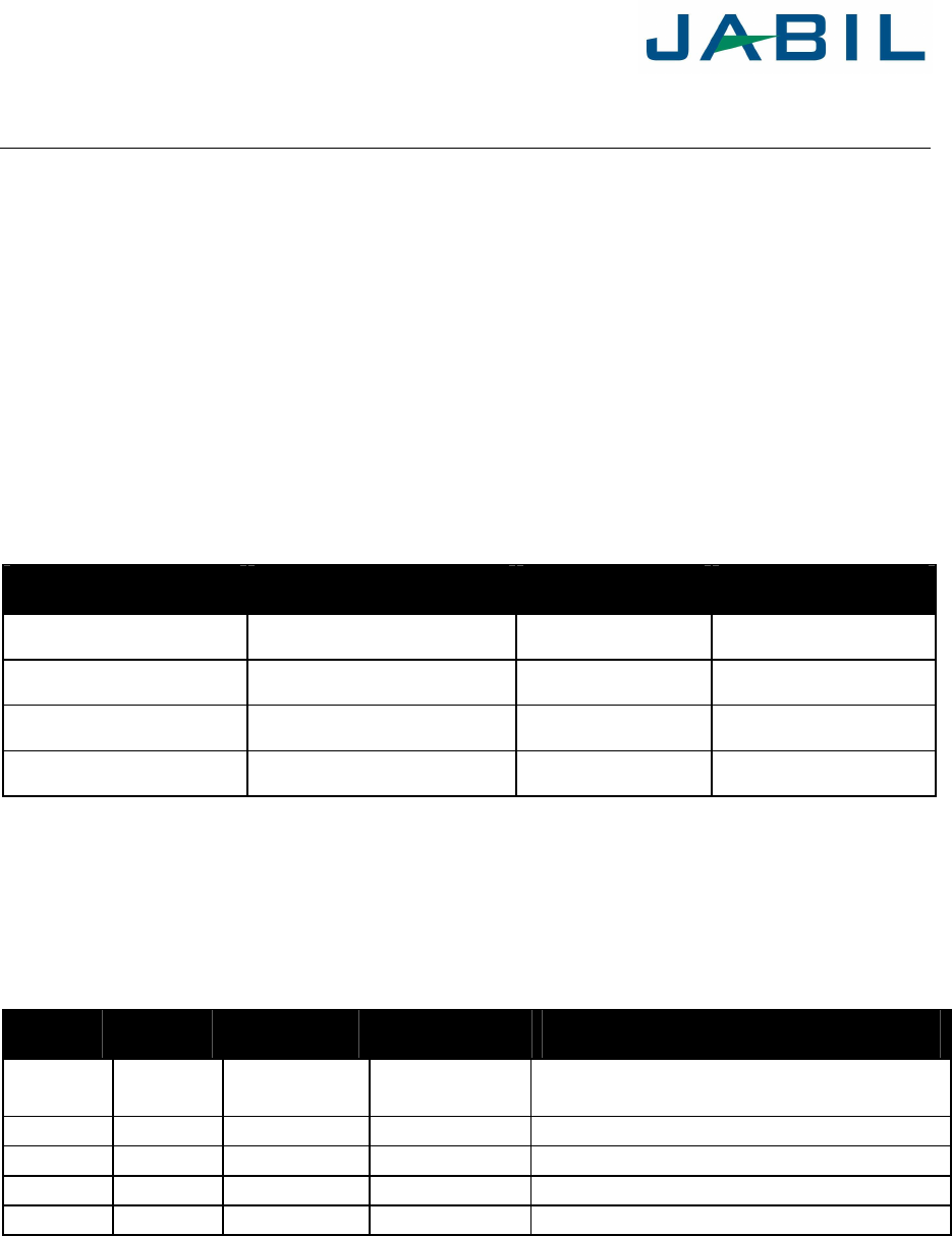
FEM Front-end module
SPI Serial Peripheral Interface
UART Universal Asynchronous Receiver Transmitter
NF Noise figure
LPZigBee Low power ZigBee Module
2 OVERVIEW
LPZigBee module mainly consists of two sections: The System-on-Chip (EM357) and
the RF front-end (SE2432L) with power amplifier and low-pass filtering.
The EM357 includes radio transceiver and microcontroller. The radio transceiver
handles all actions concerning RF modulation/demodulation, signal processing, frame
reception and transmission. MAC hardware acceleration functions are implemented
in the radio transceiver, too. Further information about the radio transceiver and the
microcontroller are available in the appropriate datasheets, refer to 1.5 references.
The RF front-end incorporates signal amplification and filtering of the transmit signal.
The degree of filtering depends on operating conditions as well as regional aspects.
Switching between reception and transmission is directly controlled by the radio
transceiver.
3 CONSTRAINTS, ASSUMPTIONS, AND DEPENDENCIES
4 FEATURES
Ultra compact size
High RX sensitivity (-103 dBm)
Outperforming link budget (123 dB)
Up to +20 dBm output power
Very low power consumption:
5 µA in Sleep mode,
30 mA in RX mode,
145 mA in TX mode@Pout is +20 dBm
Ample memory resources (256 bytes of flash memory, 12K bytes RAM, 4K bytes
EEPROM)
Wide range of interfaces (both analog and digital):
Spare GPIO,
2 ADC lines
UART
I2C
SPI
JTAG
Capability to use MAC address written into EEPROM
IEEE 802.15.4 compliance
2.4 GHz ISM band
Ember embedded software, including UART bootloader and AT command set
5 BLOCK DIAGRAM AND PORT FUNCTION
5.1 UART
P
ORT
LPZigBee Module provides four signals (RX, TX) of standard RS-232 protocol to
support user applications. The UART port is set the DCE port and connected with
other devices by D-Sub-9 Female connector. But the RX, TX connection between
RS-232 Transceiver and D-Sub-9 Female connector can be reversed by Jumpers,
allowing use of connecting straight-though or cross-wires cable.
5.2 P
ROGRAMMING AND
D
EBUG
P
ORT
The LPZigBee module can be programmed and debugged by JTAG port. It is a 20
pins header and connects with Atmel’s debugging tool.
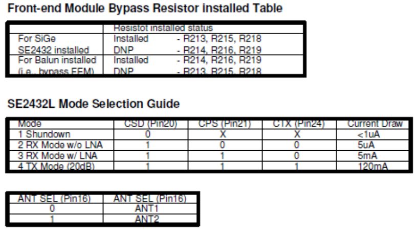
5.3 GPIO
P
ORT
The GPIO connectors provide the SPI, I2C, UART and GPIO interface for external
system testing. The recommended operation voltage is +3.3Vdc.

6 DETAIL SPECIFICATIONS
6.1 P
IN
A
SSIGNMENT
6.1.1 LPZigBee Module
Ember Function
PB3 LCD Display; SPI Chip Select, low-act;
Ember output
PA2/SPI_CLK LCD Display; SPI Clock; Ember output
PA0/SPI_MOSI LCD Display; SPI Data output from master;
Ember output
PB4 LCD Display; SPI Command/Data control,
"H"=Data, "L"=Command; Ember output
PB1/UART_TX UART to USB; Ember output
PB2/UART_RX UART to USB; Ember output
PC6 Buttons; Ember output, High-act
PC7 Buttons; Ember output, High-act
PA7 Buttons; Ember output, High-act
PA6 Buttons; Ember input, High-act
PC1 Buttons; Ember input, High-act
PA4/ADC4/PTI_EN Light sensor detect; Ember ADC input
PA5/ADC5/PTI_DATA Low power detect; Ember ADC input
PB7 Low power detect/Light sen
sor detect control
signal; Ember output, high-act
PB6/IRQB USB cable plug-in detect; Ember interrupt
input, high-act

6.2 E
LECTRICAL
S
PECIFICATION
6.2.1 DC power supply range
System module power supply range
Ember solution w/o FEM 2.1~3.6V
Ember solution with SE2432L@
NF of LNA=2 dB
Gain of LNA=12.5 dB 2.1~3.6V
6.2.2 System dBm max & min (maximum and minimum TX output at
PCB antenna) and System current & power drawn.
System module maximum TX output
minimum TX output
Ember solution w/o FEM 8dBm@I=42mA (-26)dBm@I=21mA
Ember solution with SE2432L@
NF of LNA=2 dB
Gain of LNA=12.5 dB 22dBm@Icc=NA -6dBm@>51mA
6.2.3 System current & power drawn of TX@20dBm and RX
System module TX@20dBm
RX
Ember solution w/o FEM NA I=25 mA
Ember solution with SE2432L@
NF of LNA=2 dB
Gain of LNA=12.5 dB I=145 mA I=30 mA
6.2.4 System Current and Power consumption during idle and deep
sleep mode
System module Idle mode
Deep sleep
mode
Ember solution w/o FEM
6mA @
12MHz 5µA
Ember solution with SE2432L@
NF of LNA=2 dB
Gain of LNA=12.5 dB
6mA @
12MHz
6µA

6.2.5 System RX Sensitivity (dBm)
System module
Sensitivity
(dBm)
Ember solution w/o FEM (-98.6) )
Ember solution with SE2432L@
NF of LNA=2 dB
Gain of LNA=12.5 dB (-103.53)
Federal Communication Commission Interference Statement
This module has been tested and found to comply with the limits for a Class B digital
device, pursuant to Part 15 of the FCC Rules. These limits are designed to provide
reasonable protection against harmful interference in a residential installation. This
equipment generates, uses and can radiate radio frequency energy and, if not
installed and used in accordance with the instructions, may cause harmful
interference to radio communications. However, there is no guarantee that
interference will not occur in a particular installation. If this equipment does cause
harmful interference to radio or television reception, which can be determined by
turning the equipment off and on, the user is encouraged to try to correct the
interference by one of the following measures:
- Reorient or relocate the receiving antenna.
- Increase the separation between the equipment and receiver.
- Connect the equipment into an outlet on a circuit different from that
to which the receiver is connected.
- Consult the dealer or an experienced radio/TV technician for help.
This device complies with Part 15 of the FCC Rules. Operation is subject to the
following two conditions: (1) This device may not cause harmful interference, and (2)
this device must accept any interference received, including interference that may
cause undesired operation.
FCC Caution: Any changes or modifications not expressly approved by the party
responsible for compliance could void the user's authority to operate this equipment.
IMPORTANT NOTE:
FCC Radiation Exposure Statement:
This equipment complies with FCC radiation exposure limits set forth for an
uncontrolled environment. This equipment should be installed and operated with
minimum distance 20cm between the radiator & your body.
This transmitter must not be co-located or operating in conjunction with any other
antenna or transmitter.

This device is intended only for OEM integrators under the following conditions:
1) The antenna must be installed such that 20 cm is maintained between the
antenna and users, and
2) The transmitter module may not be co-located with any other transmitter or
antenna
As long as 2 conditions above are met, further transmitter test will not be required.
However, the OEM integrator is still responsible for testing their end-product for any
additional compliance requirements required with this module installed (for example,
digital device emissions, PC peripheral requirements, etc.).
IMPORTANT NOTE: In the event that these conditions can not be met (for example
certain laptop configurations or co-location with another transmitter), then the FCC
authorization is no longer considered valid and the FCC ID can not be used on the
final product. In these circumstances, the OEM integrator will be responsible for re-
evaluating the end product (including the transmitter) and obtaining a separate FCC
authorization.
End Product Labeling
This transmitter module is authorized only for use in device where the antenna may
be installed such that 20 cm may be maintained between the antenna and users. The
final end product must be labeled in a visible area with the following: “Contains FCC
ID: ZAR-TGPBA0010260”.
Manual Information To the End User
The OEM integrator has to be aware not to provide information to the end user
regarding how to install or remove this RF module in the user’s manual of the end
product which integrates this module.
The end user manual shall include all required regulatory information/warning as
show in this manual.